

Page 1

DATA SHEET
PHOTOCOUPLERS
PS9601, PS9601L
HIGH ISOLATION VOLTAGE HIGH SPEED PHOTOCOUPLER
PS9601, PS9601L are optically coupled isolators containing a GaAlAs LED on light emitting side (input side) and
a photodiode and a signal processing circuit on light receiving side (output side) on one chip.
PS9601 is in a plastic DIP (Dual In-line Package) and PS9601L is lead bending type (Gull-wing) for surface mount.
FEATURES
• High isolation voltage BV: 5 000 Vr.m.s. MIN.
• High Propagation delay time t
• Low input current IFHL: 2.5 mA TYP.
• Can be soldered by infrared reflow soldering
• Taping product number PS9601L-E3, E4
• UL recognized File No. E72422 (S)
PHL, tPLH: 50 ns TYP.
APPLICATIONS
• Computer and peripheral memory
• Electronic instrument
• Audio-visual
Document No. P10744EJ2V0DS00 (2nd edition)
(Previous No. LC-7694)
Date Published September 1995 P
Printed in Japan
©
1993
Page 2
PS9601, PS9601L
8576
1423
V
CC
GND
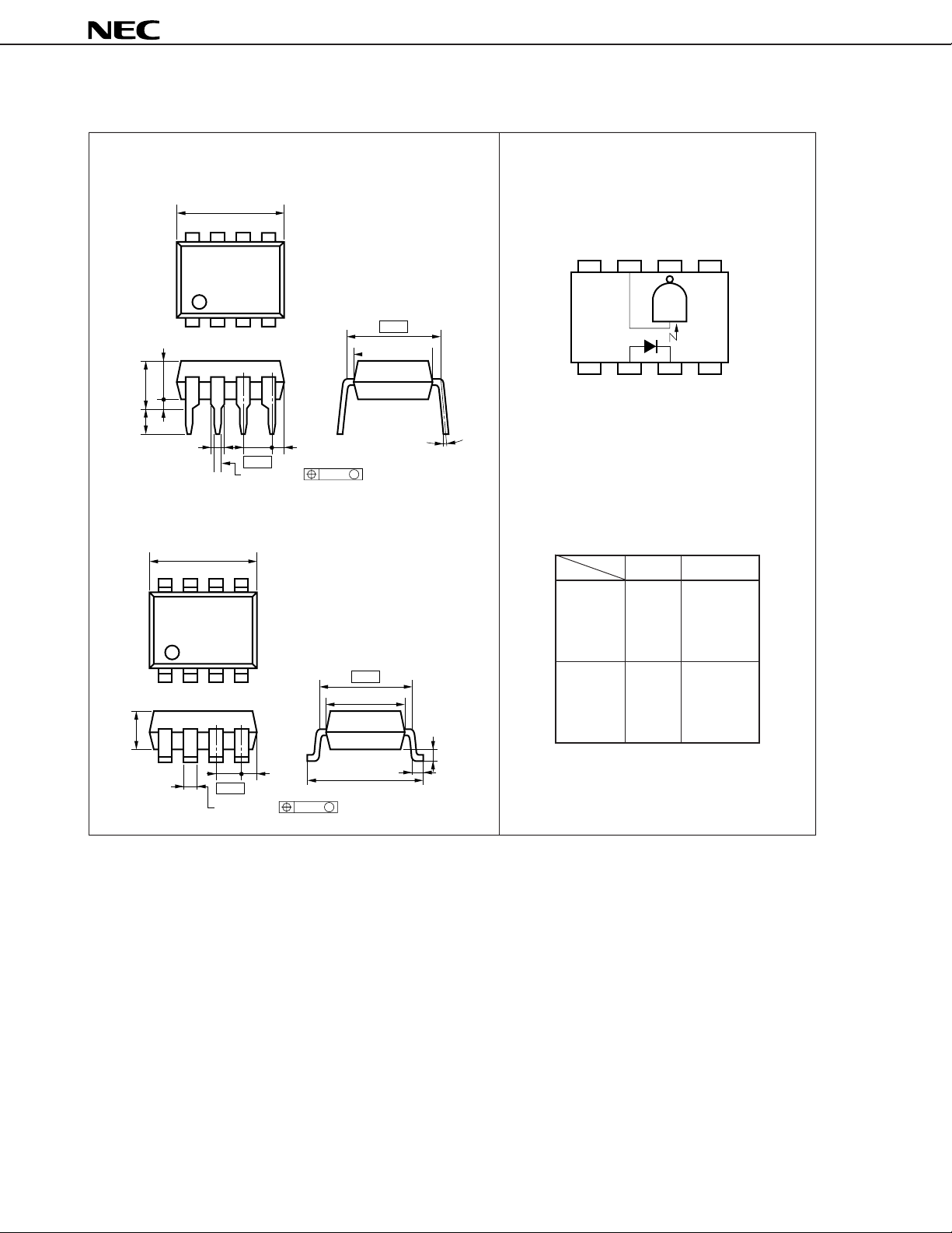
PACKAGE DIMENSIONS (Unit: mm)
PS9601 PIN CONNECTIONS (Top View)
10.16 MAX.
85
3.8
4.55
MAX.
2.8
MIN.
PS9601L
3.8
MAX.
14
MAX.
0.65
1.34
10.16 MAX.
85
14
2.54
0.50 ±0.10
2.54
1.34 ±0.10
1.27
MAX.
0.25
1.27
MAX.
0.25
9.60 ±0.4
M
M
7.62
6.5
7.62
6.5
0 to 15˚
0.05 to 0.2
0.9
±0.25
PIN Function
INPUT 1. NC
2. Anode
3. Cathode
4. NC
OUTPUT 5. GND
6. VO
7. VE*
8. VCC
*VE is pulled-up to
2
Page 3
ABSOLUTE MAXIMUM RATINGS (TA = 25 ˚C)
Diode
Forward Current IF 30 mA
Reverse Voltage VR 5V
Power Dissipation P
Detector
Supply Voltage VCC 7V
Output Voltage V
Output Current IO 50 mA
Enable Voltage VE 5.5 V
Power Dissipation P
Isolation Voltage *
1
Operating Temperature Topt –40 to +85 ˚C
Storage Temperature T
*1 AC voltage for 1 minute TA = 25 ˚C, RH = 60 % between input and output.
D 60 mW
O 7V
C 85 mW
BV 5 000 Vr.m.s.
stg –55 to +125 ˚C
PS9601, PS9601L
RECOMMENDED OPERATING CONDITIONS (TA = 25 ˚C)
PARAMETER SYMBOL MIN. TYP. MAX. UNIT
Low Level Input Current IFL 0 250
High Level Input Current IFH 71015mA
High Level Enable Voltage VEH 2VCC V
High Level Enable Voltage VEL 0 0.8 V
Supply Voltage VCC 4.5 5 5.5 V
Operating Temperature Topt 02570˚C
µ
A
* By-pass capacitor of more than 0.1 µF is used between VCC and GND near device.
ELECTRICAL CHARACTERISTICS (TA = –40 to +85 ˚C)
PARAMETER SYMBOL MIN. TYP. MAX. UNIT TEST CONDITIONS
Forward Voltage VF 1.4 1.65 1.9 V IF = 10 mA, TA = 25 ˚C
DiodeDetector
Reverse Current IR 10
Capacitance Ct 60 pF V = 0, f = 1 MHz, TA = 25 ˚C
High Level Output Current IOH 2 250
Low Level Output Voltage VOL 0.2 0.6 V
High Level Supply Current ICCH 5710mAVCC = 5.5 V, VE = 0.5 V, IF = 0
Low Level Supply Current ICCL 10 13 18 mA VCC = 5.5 V, VE = 2 V, IF = 10 mA
High Level Enable Current IEH –0.7 –1 –1.5 mA VCC = 5.5 V, VEH = 2 V
Low Level Enable Current IEL –1 –1.4 –2 mA VCC = 5.5 V, VEL = 0.5 V
µ
AVR = 5 V, TA = 25 ˚C
µ
AVCC = VO = 5.5 V, IF = 250 µs, VE = 2 V
VCC = 5.5 V, IF = 5 mA, VE = 2 V, IO = 13 mA
3
Page 4

ELECTRICAL CHARACTERISTICS (TA = 25 ˚C)
PARAMETER SYMBOL MIN. TYP. MAX. UNIT TEST CONDITIONS
Treshold Input Current IFHL 0.5 2.5 5 mA VCC = 5 V, VE = 2 V, TA = –40 to + 85 ˚C
High → Low VO = 0.8 V, RL = 350 Ω
Isolation Resistance R1-2 10
Isolation Capacitance C1-2 0.6 pF V = 0, f = 1 MHz
Propagation Delay Time*
2
tPHL 50 75 ns VCC = 5 V, IF = 7.5 mA
High → Low RL = 350 Ω, CL = 15 pF
Propagation Delay Time*
2
tPLH 50 75 ns
Low → High
Coupled
Rise Time tr 20 ns
Fall Time tf 10 ns
Enable Propagation tEHL 10 ns VCC = 5 V, IF = 7.5 mA
Delay Time*
3
High → Low RL = 350 Ω, CL = 15 pF
Enable Propagation tELH 25 ns
Delay Time*
3
Low → High
11
PS9601, PS9601L
Ω Vin-out = 1 kVDC, RH 40 to 60 %
VEH = 3 V, VEL = 0.5 V
*2 Test Circuit for Propagation delay time
Pulse Input
8
PW = 1 s
µ
duty cycle = 1/10
IF Monitor
47 Ω
1
I
F
2
3
4
V
GND
CC
7
6
5
* CL is approximately 15 pF, which includes probe and stray wiring capacitance.
0.1
µ
V
CC
= 5 V
Input
R
L
F
= 350 Ω
VO Monitor
*C
L
0
5 V
Output
*3 Test Circuit for enable Propagation delay time
Pulse Input
PW = 1 s
duty cycle = 1/10
IF = 7.5 mA
VE
µ
1
2
3
8
µ
F
7
0.1
6
5 V
Monitor
RL = 350 Ω
VO
*CL
4
5
VE
V
350 mV
(I
F
= 7.5 mA)
175 mV
(I
F
= 3.75 mA)
1.5 V
V
OL
PHL
t
t
PLH
3 V
1.5 V
tEHL tELH
0.5 V
5 V
O
1.5 V
VOL
4
Page 5

TYPICAL CHARACTERISTICS (TA = 25 ˚C)
PS9601, PS9601L
MAX. FORWARD CURRENT vs.
AMBIENT TEMPERATURE
50
40
30
20
10
- MAX. Forward Current - mA
F
I
0 20406080100
T
A
- Ambient Temperature - ˚C
FORWARD CURRENT vs.
FORWARD VOLTAGE
100
10
1.0
0.1
- Forward Current - mA
F
I
TA = 100 ˚C
50 ˚C
25 ˚C
0 ˚C
–25 ˚C
0.01
1.0 2.41.2 1.4 1.6 1.8 2.0 2.2
V
F
- Forward Voltage - V
POWER DISSIPATION vs.
AMBIENT TEMPERATURE
100
80
60
40
- Power Dissipation - mA
C
20
P
0 20406080100
T
A
- Ambient Temperature - ˚C
THRESHOLD CURRENT vs.
AMBIENT TEMPERATURE
10
8
VCC = 5 V
VE = 2 V
VO = 0.8 V
RL = 350 Ω
6
4
2
- Threshold Input Current - mA
FHL
I
0
–50 –25 0 25 50 75
100
TA - Ambient Temperature - ˚C
OUTPUT VOLTAGE vs.
FORWARD CURRENT
7
5 V
L
6
R
V
O
1.0
0.8
LOW LEVEL OUTPUT VOLTAGE
vs. AMBIENT TEMPERATURE
5
4
3
- Output Voltage - V
2
O
V
1
L
= 100 Ω
R
RL = 350 Ω
RL = 1 kΩ
0.6
0.4
0.2
- Low Level Output Voltage - V
OL
V
0
012
246810
I
F
- Forward Current - mA
–50 –25 0 25 50 75
TA - Ambient Temperature - ˚C
VCC = 5 V
VE = 2 V
IF = 5 mA
IO = 13 mA
100
5
Page 6

PS9601, PS9601L
PROPAGATION DELAY TIME
vs. FORWARD CURRENT
80
t
PLH
60
40
t
PHL
20
- Propagation Delay Time - ns
PLH
, t
PHL
t
0 5 10 15 20 25
F
- Forward Current - mA
I
PROPAGATION DELAY TIME
vs. AMBIENT TEMPERATURE
120
100
80
t
60
PLH
40
t
- Propagation Delay Time - ns
20
PLH
, t
PHL
t
0
–50
–25 0 25 50 75 100
A
- Ambient Temperature - ˚C
T
PHL
VCC =
5 V
RL =
350 Ω
IF = 7.5 mA
VCC = 5 V
RL = 350 Ω
PROPAGATION DELAY TIME vs.
LOAD RESISTANCE
1 000
500
100
t
PLH
50
- Propagation Delay Time - ns
PLH
, t
PHL
t
10
100
t
PHL
500 1 k 5 k 10 k 50 k
L
- Load Resistance - Ω
R
SWITCHING TIME vs.
AMBIENT TEMPERATURE
25
20
15
10
- Swiching Time - ns
f
, t
r
t
5
0
–50
–25 0 25 50 75 100
A
- Ambient Temperature - ˚C
T
I
V
PW = 1 s,
duty 1/10
t
r
t
f
F
= 7.5 mA
CC
= 5 V
µ
IF = 7.5 mA
VCC = 5 V
RL = 350 Ω
ENABLE PROPAGATION DELAY TIME
vs. AMBIENT TEMPERATURE
60
40
t
20
ELH
- Enable Propagation Delay Time - ns
ELH
, t
EHL
t
0
–25 0 25 50 75 100
–50
A
- Ambient Temperature - ˚C
T
t
EHL
IF = 7.5 mA
VCC = 5 V
VEH = 3 V
VEL = 0.5 V
RL = 350 Ω
6
Page 7

PS9601, PS9601L
PRECAUTIONS IN MOUNTING THE DEVICE
(1) Precautions in mounting the device by infrared reflow soldering
• Peak reflow temperature : 235 ˚C or below (Plastic surface temperature)
• Reflow time : 30 seconds or less (Time period during which the plastic surface temperature
is 210 ˚C)
• Number of reflow processes: One
• Flux : Rosin flux containing small amount of chlorine (The flux with a maximum
chlorine content of 0.2 Wt% is recommended.)
INFRARED RAY REFLOW TEMPERATURE PROFILE
(Actual heat)
to 10 s
235 ˚C Peak
210 ˚C
to 30 s
120 to 160 ˚C
60 to 90 s
(Pre-heat)
Package’s Surface Temperature (˚C)
Times (s)
Peak Temperature 230 ˚C
or Lower
(2) Precautions in mounting the device in solder dip method
• Temperature : 260 ˚C or lower
• Time : 10 sec. or less
• Flux : Rosin group flux, where the amount of chloride component is small.
7
Page 8

PS9601, PS9601L
Caution
The Great Care must be taken in dealing with the devices in this guide.
The reason is that the material of the devices is GaAs (Gallium Arsenide), which is
designated as harmful substance according to the law concerned.
Keep the law concerned and so on, especially in case of removal.
No part of this document may be copied or reproduced in any form or by any means without the prior written
consent of NEC Corporation. NEC Corporation assumes no responsibility for any errors which may appear in this
document.
NEC Corporation does not assume any liability for infringement of patents, copyrights or other intellectual
property rights of third parties by or arising from use of a device described herein or any other liability arising
from use of such device. No license, either express, implied or otherwise, is granted under any patents,
copyrights or other intellectual property rights of NEC Corporation or others.
While NEC Corporation has been making continuous effort to enhance the reliability of its semiconductor devices,
the possibility of defects cannot be eliminated entirely. To minimize risks of damage or injury to persons or
property arising from a defect in an NEC semiconductor device, customer must incorporate sufficient safety
measures in its design, such as redundancy, fire-containment, and anti-failure features.
NEC devices are classified into the following three quality grades:
“Standard“, “Special“, and “Specific“. The Specific quality grade applies only to devices developed based on
a customer designated “quality assurance program“ for a specific application. The recommended applications
of a device depend on its quality grade, as indicated below. Customers must check the quality grade of each
device before using it in a particular application.
Standard: Computers, office equipment, communications equipment, test and measurement equipment,
audio and visual equipment, home electronic appliances, machine tools, personal electronic
equipment and industrial robots
Special: Transportation equipment (automobiles, trains, ships, etc.), traffic control systems, anti-disaster
systems, anti-crime systems, safety equipment and medical equipment (not specifically designed
for life support)
Specific: Aircrafts, aerospace equipment, submersible repeaters, nuclear reactor control systems, life
support systems or medical equipment for life support, etc.
The quality grade of NEC devices in “Standard“ unless otherwise specified in NEC's Data Sheets or Data Books.
If customers intend to use NEC devices for applications other than those specified for Standard quality grade,
they should contact NEC Sales Representative in advance.
Anti-radioactive design is not implemented in this product.
M4 94.11
2
 Loading...