

Page 1
DATA SHEET
PHOTOCOUPLER
PS8701
HIGH NOISE REDUCTION HIGH-SPEED ANALOG OUTPUT TYPE
5-PIN SOP PHOTOCOUPLER
DESCRIPTION
The PS8701 is an optically coupled isolator containing a GaAlAs LED on the light emitting diode (input side) and a
PIN photodiode and a high-speed amplifier transistor on the output side on one chip.
This is a plastic SOP (Small Out-line Package) type for high density applications.
FEATURES
• High common mode transient immunity (CMH, CML = ±10 kV/µs MIN.)
• High supply voltage (VCC = 35 V)
• High isolation voltage (BV = 2 500 Vr.m.s.)
• High-speed response (t
PHL
= 0.8 µs MAX., t
• Taping product number (PS8701-E3, E4, F3, F4)
PLH
= 1.2 µs MAX.)
APPLICATIONS
• Computer and peripheral manufactures
• General purpose inverter
• Substitutions for relays and pulse transformers
• Power supply
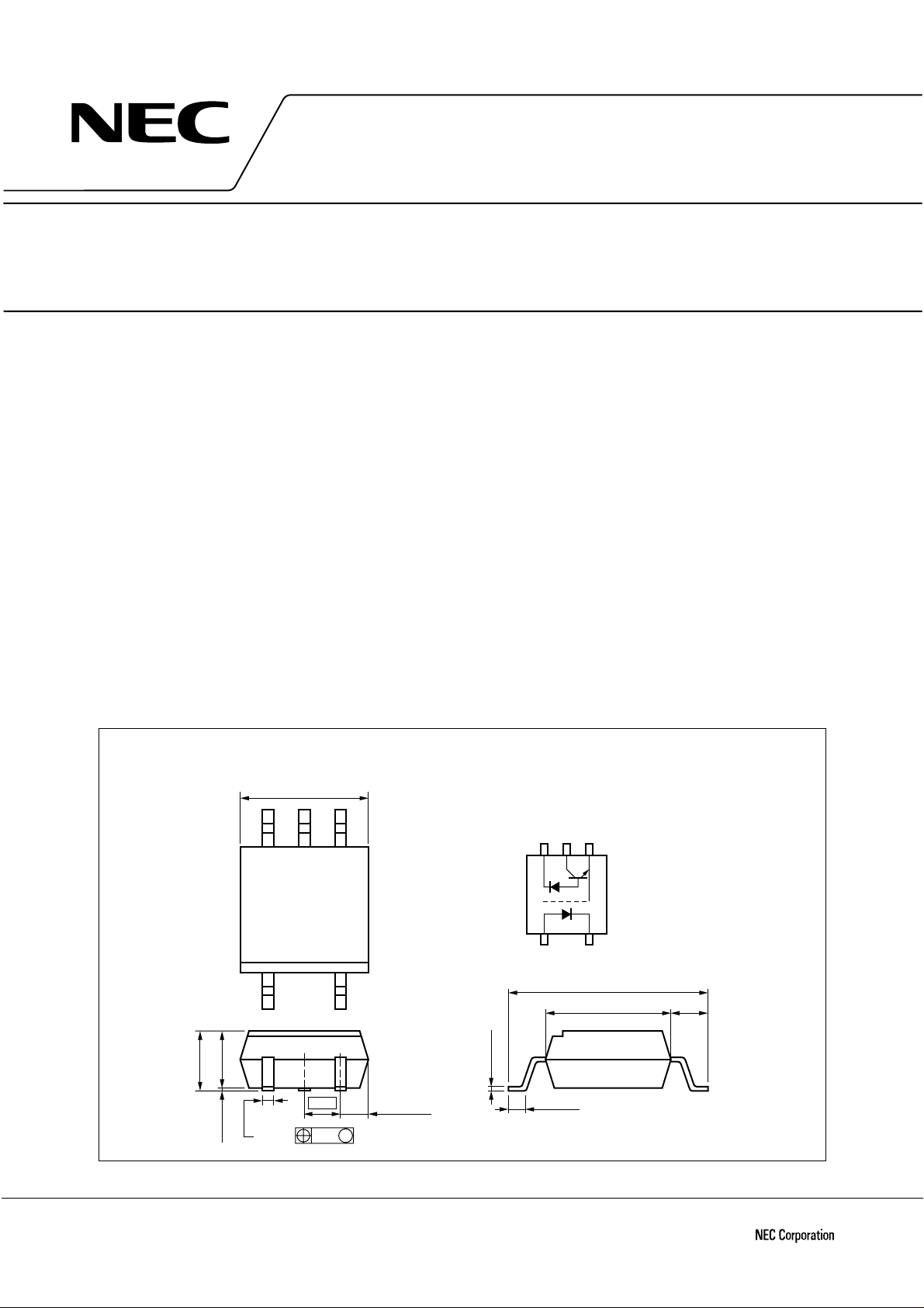
PACKAGE DIMENSIONS
4.5 MAX.
2.00.1±0.1
2.3 MAX.
0.4
+0.10
–0.05
1.27
0.25 M
1.2 MAX.
in millimeters
+0.10
–0.05
0.15
TOP VIEW
53
4
12
7.0±0.3
4.4
0.5±0.3
1. Anode
2. Cathode
3. GND
O
4. V
5. V
CC
1.3
The information in this document is subject to change without notice.
Document No. P12846EJ1V0DS00 (1st edition)
Date Published August 1997 NS
Printed in Japan
©
1997
Page 2

ABSOLUTE MAXIMUM RATINGS (TA = 25 °C, unless otherwise specified)
Parameter Symbol Ratings Unit
PS8701
Diode Forward Current I
Reverse Voltage V
Power Dissipation P
Detector Supply Voltage V
Output Voltage V
Output Current I
Power Dissipation P
Isolation Voltage
*1
Operating Ambient Temperature T
Storage Temperature T
AC voltage for 1 minute at T
*1
F
R
D
CC
O
O
C
25 mA
3.0 V
45 mW
35 V
35 V
8.0 mA
100 mW
BV 2 500 Vr.m.s.
A
stg
A
= 25 °C, RH = 60 % between input and output
–55 to +100 °C
–55 to +125 °C
ELECTRICAL CHARACTERISTICS (TA = 25 °C)
Parameter Symbol Conditions MIN. TYP. MAX. Unit
Diode Forward Voltage V
Reverse Current I
Forward Voltage
Temperature Coefficient
Terminal Capacitance C
Detector High Level Output Current IOH (1) IF = 0 mA, VCC = VO = 5.5 V 3 500 nA
High Level Output Current IOH (2) IF = 0 mA, VCC = VO = 30 V 100
Low Level Output Voltage V
Low Level Supply Current I
High Level Supply Current I
Coupled Current Transfer Ratio CTR IF = 16 mA, VCC = 4.5 V, VO = 0.4 V 15 20 35 %
Isolation Resistance R
Isolation Capacitance C
Propagation Delay Time
*1
(H → L)
Propagation Delay Time
*1
(L → H)
Common Mode
Transient Immunity at
High Level Output
*2
Common Mode
Transient Immunity at
Low Level Output
*2
F
IF = 16 mA 1.7 2.2 V
R
VR = 3 V 10
∆
VF/∆TIF = 16 mA
t
V = 0 V, f = 1 MHz 60 pF
OLIF
= 16 mA, VCC = 4.5 V, IO = 1.2 mA 0.1 0.4 V
CCLIF
CCHIF
PHL
t
PLH
t
C
C
= 16 mA, VO = open, VCC = 30 V 50
= 0 mA, VO = open, VCC = 30 V 0.01 2
I-O
I-O
V
= 1 kVDC, RH = 40 to 60 % 10
I-O
V = 0 V, f = 1 MHz 0.4 pF
IF = 16 mA, VCC = 5 V, RL = 2.2 kΩ,
L
= 15 pF
C
IF = 0 mA, VCC = 5 V, RL = 4.1 kΩ,
MH
CM
= 1.5 kV
V
IF = 16 mA, VCC = 5 V, RL = 4.1 kΩ,
ML
CM
= 1.5 kV
V
−
1.6 mV/°C
11
0.5 0.8
0.6 1.2
10 kV/
−
10
µ
A
µ
A
µ
A
Ω
µ
s
µ
s
2
Page 3
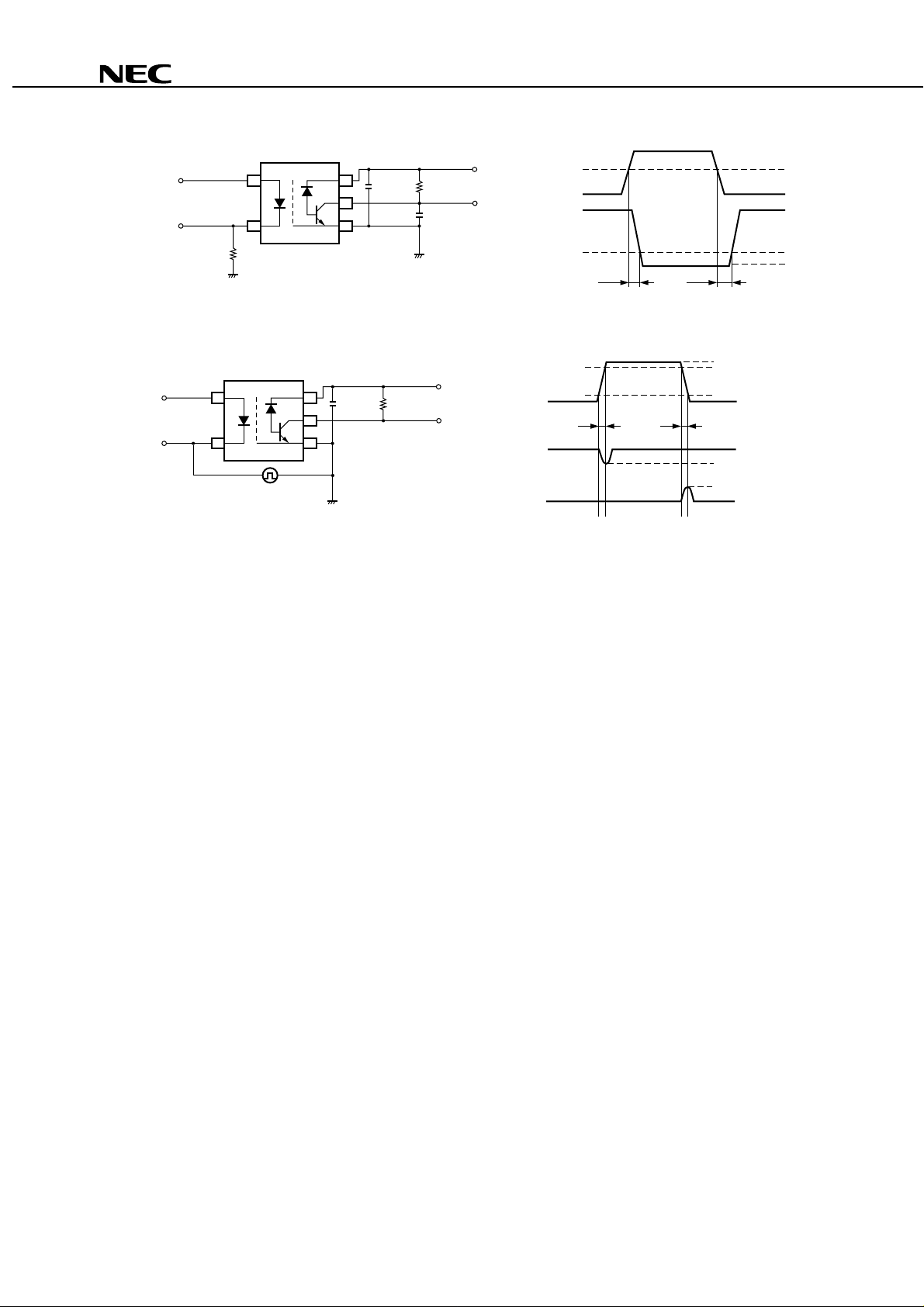
Test circuit for propagation delay time
*1
V
CC
Pulse input
(Pulse width = 100 s,
µ
Duty cycle = 1/10)
µ
0.1 F
RL = 2.2 kΩ
CL = 15 pF
= 5 V
VO (Monitor)
Input
(Monitor)
47 Ω
CL is approximately 15 pF which includes probe and stray wiring capacitance
Test circuit for common mode transient immunity
*2
VCM
V
IF
µ
0.1 F
RL = 4.1 kΩ
CC = 5 V
VO (Monitor)
Input
Output
t
90 %
10 %
tr tf
PHL
PS8701
50 %
5 V
1.5 V
OL
t
PLH
1.5 kV
V
0 V
VCM
VO
F = 0 mA)
(I
V
O
F = 16 mA)
(I
2 V
0.8 V
5 V
V
OL
USAGE CAUTIONS
1. This product is weak for static electricity by designed with high-speed integrated circuit so protect against static
electricity when handling.
2. By-pase capacitor of more than 0.1 µF is used between VCC and GND near device.
3
Page 4

TYPICAL CHARACTERISTICS (TA = 25 °C, unless otherwise specified)
PS8701
DIODE POWER DISSIPATION vs.
AMBIENT TEMPERATURE
50
40
30
20
10
Diode Power Dissipation PD (mW)
0
25 50 75 100
Ambient Temperature T
FORWARD CURRENT vs.
FORWARD VOLTAGE
100
TA = +100 ˚C
10
1
+50 ˚C
+25 ˚C
0 ˚C
–25 ˚C
A (˚C)
TRANSISTOR POWER DISSIPATION vs.
AMBIENT TEMPERATURE
120
100
80
60
40
20
Transistor Power Dissipation PC (mW)
0
25 50 75 100
Ambient Temperature T
A (˚C)
HIGH LEVEL OUTPUT CURRENT vs.
AMBIENT TEMPERATURE
1 000
IF = 0 mA
100
VCC = VO = 30 V
CC = VO = 5.5 V
10
V
0.1
Forward Current IF (mA)
0.01
1.4 1.8 2.0 2.41.0 1.2 1.6 2.2
Forward Voltage V
CURRENT TRANSFER RATIO vs.
FORWARD CURRENT
80
)
70
%
60
50
40
30
20
10
Current Transfer Ratio CTR (
0
0.5 5 10 501
Forward Current I
F (V)
F (mA)
VCC = 4.5 V,
O = 0.4 V
V
1
High Level Output Current IOH (nA)
0.1
Ambient Temperature T
50 100–25 0 25 75
A (˚C)
NORMALIZED CURRENT TRANSFER
RATIO vs. AMBIENT TEMPERATURE
1.6
1.4
1.2
1.0
0.8
0.6
0.4
0.2
Normalized Current Transfer Raio CTR
0.0
Ambient Temperature T
Normalized to 1.0
A = 25 ˚C, IF = 16 mA,
at T
CC = 4.5 V, VO = 0.4 V
V
0 50 100–50 –25 25
A (˚C)
75
4
Page 5

PS8701
10
Output Current IO (mA)
3.0
µ
2.0
OUTPUT CURRENT vs.
OUTPUT VOLTAGE
8
IF = 25 mA
6
20 mA
15 mA
4
10 mA
2
0
4 8 18 20162 6 10 12 14
5 mA
Output Voltage V
O (V)
PROPAGATION DELAY TIME vs.
FORWARD CURRENT
VCC = 5 V,
L = 2.2 kΩ
R
Output Voltage VO (V)
µ
OUTPUT VOLTAGE vs.
FORWARD CURRENT
6
5
4
3
2
1
0
RL = 2.2 kΩ
5.6 kΩ
4826
Forward Current I
10
12
F (mA)
PROPAGATION DELAY TIME vs.
LOAD RESISTANCE
10
t
PLH
16
14
VCC = 5 V,
F = 16 mA
I
18
20
PHL
t
1.0
Propagation Delay Time tPHL, tPLH ( s)
tPLH
0
5
10 15
Forward Current I
20
F (mA)
25
NORMALIZED PROPAGATION DELAY TIME
vs. AMBIENT TEMPERATURE
5
4
3
2
1
0
–25
–50 0 50
Normalized Propagation Delay Time tPHL, tPLH
Ambient Temperature T
Normalized to 1.0
A = 25 ˚C,
at T
F = 16 mA, VCC = 5 V,
I
L = 2.2 kΩ
R
PLH
t
tPHL
7525
A (˚C)
100
Propagation Delay Time tPHL, tPLH ( s)
0.1
1
1 k
tPHL
10 k
Load Resistance R
100 k
L (Ω)
5
Page 6

TAPING SPECIFICATIONS (in millimeters)
Outline and Dimensions (Tape)
2.0±0.1
4.0±0.1
1.55±0.1
1.75±0.1
PS8701
2.4±0.1
1.55±0.1
8.0±0.1
Taping Direction
PS8701-E3
PS8701-F3
Outline and Dimensions (Reel)
4.6±0.1
1
2
0
5.5±0.1
˚
12.0±0.2
PS8701-E4
PS8701-F4
0.3
7.4±0.1
1.5±0.1
1.5±0.1
21.0±0.8
φ
2.0±0.5
1.5±0.5
6
0
˚
6.0±1
Packing: PS8701-E3, E4 900 pcs/reel
φ
φ
66
φ
13.0±0.5
φ
PS8701-E3, E4: 178
PS8701-F3, F4: 330
+2.0
12.4
–0.0
18.4 MAX.
PS8701-F3, F4 3 500 pcs/reel
6
Page 7

RECOMMENDED SOLDERING CONDITIONS
(1) Infrared reflow soldering
• Peak reflow temperature 235 °C (package surface temperature)
• Time of temperature higher than 210 °C 30 seconds or less
• Number of reflows Three
• Flux Rosin flux containing small amount of chlorine (The flux with a
maximum chlorine content of 0.2 Wt % is recommended.)
Recommended Temperature Profile of Infrared Reflow
(heating)
to 10 s
235 ˚C (peak temperature)
210 ˚C
to 30 s
120 to 160 ˚C
PS8701
60 to 90 s
(preheating)
Package Surface Temperature T (˚C)
Time (s)
Caution
Please avoid to removed the residual flux by water after the first reflow processes.
Peak temperature 235 ˚C or below
(2) Dip soldering
• Temperature 260 °C or below (molten solder temperature)
• Time 10 seconds or less
• Number of times One
• Flux Rosin flux containing small amount of chlorine (The flux with a maximum chlorine content of
0.2 Wt % is recommended.)
7
Page 8

CAUTION
Within this device there exists GaAs (Gallium Arsenide) material which is a
harmful substance if ingested. Please do not under any circumstances break the
hermetic seal.
PS8701
No part of this document may be copied or reproduced in any form or by any means without the prior written
consent of NEC Corporation. NEC Corporation assumes no responsibility for any errors which may appear in this
document.
NEC Corporation does not assume any liability for infringement of patents, copyrights or other intellectual
property rights of third parties by or arising from use of a device described herein or any other liability arising
from use of such device. No license, either express, implied or otherwise, is granted under any patents,
copyrights or other intellectual property rights of NEC Corporation or others.
While NEC Corporation has been making continuous effort to enhance the reliability of its semiconductor devices,
the possibility of defects cannot be eliminated entirely. To minimize risks of damage or injury to persons or
property arising from a defect in an NEC semiconductor device, customers must incorporate sufficient safety
measures in its design, such as redundancy, fire-containment, and anti-failure features.
NEC devices are classified into the following three quality grades:
"Standard", "Special", and "Specific". The Specific quality grade applies only to devices developed based on
a customer designated "quality assurance program" for a specific application. The recommended applications
of a device depend on its quality grade, as indicated below. Customers must check the quality grade of each
device before using it in a particular application.
Standard: Computers, office equipment, communications equipment, test and measurement equipment,
audio and visual equipment, home electronic appliances, machine tools, personal electronic
equipment and industrial robots
Special: Transportation equipment (automobiles, trains, ships, etc.), traffic control systems, anti-disaster
systems, anti-crime systems, safety equipment and medical equipment (not specifically designed
for life support)
Specific: Aircrafts, aerospace equipment, submersible repeaters, nuclear reactor control systems, life
support systems or medical equipment for life support, etc.
The quality grade of NEC devices is "Standard" unless otherwise specified in NEC's Data Sheets or Data Books.
If customers intend to use NEC devices for applications other than those specified for Standard quality grade,
they should contact an NEC sales representative in advance.
Anti-radioactive design is not implemented in this product.
M4 96. 5
 Loading...