

Page 1

1
PS8168C 03/24/00
Top View
Features
Low On-Resistance, (16Ω typ) Minimizes Distortion
and Error Voltages
On-Resistance Match Between Channels, <2Ω
Guaranteed On-Resistance Flatness, <4Ω
Low Charge Injection, 3pC typ.
Improved Leakage Over Temperature, <2.5nA at +85oC
ESD Rating >2000V per Method 3015.7
Single-Supply Operation (+3V to +15V)
Bipolar-Supply Operation (±3V to ±8V)
Low Power Consumption, <1µA
TTL/CMOS Compatible
Description
The PS391/ PS392/ PS393 are improved, quad, single-pole singlethrow (SPST) analog switches designed to operate with +3V to ±8V
power supplies. The PS391 has four normally closed (NC) switches,
the PS392 has four normally open (NO) switches. The PS393
has two NO and two NC switches. All three devices offer
low leakage (<2pA typ) and fast switching speeds (tON <130ns).
Power consumption is less than 1µA, ideal for battery-powered
equipment.
With ±5V supplies, the PS391/PS392/PS393 guarantee <2Ω
channel-to-channel matching, <30Ω on-resistance (RON), and <4Ω
RON flatness over the specified range.
These switches are fully specified for single +5V operation, with
<2Ω RON match, <45Ω RON, and <4Ω flatness.
For operation below 5V, the PI5A391A/PI5A392A/PI5A393A are
also recommended.
12345678901234567890123456789012123456789012345678901234567890121234567890123456789012345678901212345678901234567890123456789012123456789012
12345678901234567890123456789012123456789012345678901234567890121234567890123456789012345678901212345678901234567890123456789012123456789012
PS391/PS392/PS393
Precision, Quad, SPST, Analog Switches
Functional Diagrams, Pin Configurations, and Truth Tables
N.C. = No Connect. Switches shown for logic “0” input
Top View
Top View
14
15
16
9
13
12
11
10
1
2
3
4
5
7
6
8
IN1
COM1
NC1
V-
GND
NC4
IN4
COM4
IN2
NC2
V
N.C.
NC3
COM3
IN3
COM2
PS391
+
14
15
16
9
13
12
11
10
1
2
3
4
5
7
6
8
IN1
COM1
NO1
V-
GND
NO4
IN4
COM4
IN2
NO2
V+
N.C.
NO3
COM3
IN3
COM2
PS392
14
15
16
9
13
12
11
10
1
2
3
4
5
7
6
8
IN1
COM1
NO1
V-
GND
NO4
IN4
COM4
IN2
NC2
V
N.C.
NC3
COM3
IN3
COM2
PS393
+
193SP
cigoLhctiwS
0
1
NO
FFO
393SP
cigoL4,1sehctiwS3,2sehctiwS
0
1
FFO
NO
NO
FFO
293SP
cigoLhctiwS
0
1
FFO
NO
Applications
• Instrumentation
• Battery Powered Systems
• Audio Switching
• ±5V Data Acquisition Systems
• Sample-and-Hold Circuits
• Telecommunications Systems
Page 2

12345678901234567890123456789012123456789012345678901234567890121234567890123456789012345678901212345678901234567890123456789012123456789012
2
PS8168C 03/24/00
PS391/PS392/PS393
Precision, Quad, SPST Analog Switches
Absolute Maximum Ratings
Caution: Stresses beyond those listed under “Absolute Maximum Ratings” may cause permanent damage to the device. This is a stress only
rating and operation of the device at these or any other conditions beyond those indicated in the operational sections of this specification is not
implied.
Electrical Specifications - Single +12V Supply
(V+ = 12V ±10%, GND = 0V, V
INH
= 4V, V
INL
= 0.8V)
Thermal Information
Continuous Power Dissipation (TA= +70ºC)
Plastic DIP (derate 10.5mW/ ºC above +70ºC) . . . . . . . . . 800mW
SO and QSOP (derate 8.7mW/ ºC above +70ºC) . . . . . . . 650mW
Storage Temperature . . . . . . . . . . . . . . . . . . . . –65ºC to +150ºC
Lead Temperature (soldering, 10s) . . . . . . . . . . . . . . . . . +300ºC
Note
Signals on NC, NO, COM, or IN exceeding V+ or GND are clamped
by internal diodes. Limit forward diode current to 30mA.
Voltages Referenced to GND
V+ . . . . . . . . . . . . . . . . . . . . . . . . . . . . . . . . . . –0.3V to +17V
VIN, V
COM
, VNC, VNO (Note 1) . . . . . . . . . . . . –2V to (V+) +2V
or 30mA, whichever occurs first
Current (any terminal) . . . . . . . . . . . . . . . . . . . . . . . . . . 30mA
Peak Current, COM, NO, NC
(pulsed at 1ms, 10% duty cycle) . . . . . . . . . . . . . . . . . 100mA
ESD per Method 3015.7. . . . . . . . . . . . . . . . . . . . . . . . >2000V
retemaraPlobmySsnoitidnoC)C°(.pmeTniM
(1)
pyT
(2)
xaM
(1)
stinU
hctiwSgolanA
egnaRlangiSgolanA
)3(
V
GOLANA
lluF0 +VV
ecnatsiseRnOR
NO
I,V21=+V
MOC
,Am2=
V
ON
V01=
526154
Ω
lluF55
hctaMecnatsiseR-nO
slennahCneewteB
)4(
∆R
NO
I,V21=+V
MOC
Am2=
V
ON
V01=
525.04
lluF6
ecnatsiseR-nO
ssentalF
)5(
R
)NO(TALF
I,V21=+V
MOC
,Am2=
V
ON
V1,V5,V01=
5224
lluF6
ffOCNroON
tnerruCegakaeL
)6(
I
)FFO(ON
OR
I
)FFO(CN
V,V21=+V
MOC
,V0=
V
ON
V01=
5211
An
lluF66
egakaeLffOMOC
tnerruC
)6(
I
)FFO(MOC
V,V21=+V
MOC
,V0=
V
ON
V01=
5211
lluF66
egakaeLnOMOC
tnerruC
)6(
I
)NO(MOC
V,V21=+V
MOC
,V01=
V
ON
V01=
5222
lluF2121
Page 3

12345678901234567890123456789012123456789012345678901234567890121234567890123456789012345678901212345678901234567890123456789012123456789012
12345678901234567890123456789012123456789012345678901234567890121234567890123456789012345678901212345678901234567890123456789012123456789012
PS391/PS392/PS393
Precision, Quad, SPST Analog Switches
3
PS8168C 03/24/00
Electrical Specifications - Single +12V Supply (continued)
(V+ = 12V ±10%, GND = 0V, V
INH
= 4V, V
INL
= 0.8V)
Notes:
1 . The algebraic convention, where the most negative value is a minimum and the most positive is a maximum, is used in
this data sheet.
2 . Typical values are for DESIGN AID ONLY, not guaranteed or subject to production testing.
3. Guaranteed by design
4. ∆R
ON
=
∆R
ON
max - ∆R
ON
min
5 . Flatness is defined as the difference between the maximum and minimum value of on-resistance measured.
6 . Leakage parameters are 100% tested at maximum rated hot temperature and guaranteed by correlation at +25ºC.
7 . Off Isolation = 20log10 [ V
COM
/ (VNO or VNO) ], V
COM
= 0utput, VNC /V
NO
=
input to off switch
8. Between any two switches.
retemaraPlobmySsnoitidnoC)C°(pmeTniM
)1(
pyT
)2(
xaM
)1(
stinU
tupnIcigoL
tupnIhtiwtnerruCtupnI
hgiHegatloV
I
HNI
I
N
V8.0=srehtolla,V5=
lluF
5.0500.05.0
µA
tupnIhtiwtnerruCtupnI
woLegatloV
I
LNI
I
N
V5=srehtolla,V8.0=5.0500.05.0
cimanyD
emiTnO-nruTt
NO
V
MOC
2erugiF,V01=
5215031
sn
lluF571
emiTffO-nruTt
FFO
527157
lluF001
htdiwdnaBlennahC-nOWB
mbd0=langiS
05,4erugiF Ω tuodnani
52
001zHM
noitcejnIegrahC
)3(
Q
C
L
,Fn1=V
NEG
R,V0=
NEG
0= Ω,
3erugiF
301Cp
noitalosIffOO
RRI
R
L
05= Ω C,
L
4erugiF,zHM1=f,Fp5=85
Bd
klatssorC
)8(
X
KLAT
R
L
05= Ω C,
L
5erugiF,zHM1=f,Fp5=68
ecnaticapaCONC
)FFO(
6erugiF,zHM1=f21
Fp
ecnaticapaCffOMOCC
)FFO(MOC
6erugiF,zHM1=f21
ecnaticapaCnOMOCC
)NO(MOC
7erugiF,zHM1=f52
tnerruCylppuSevitisoP+IV
NI
fforonoslennahclla,+VroV0=
lluF
1 100.01
µA
noitrotsiDcinomraHlatoTDHT 30.0%
Page 4

12345678901234567890123456789012123456789012345678901234567890121234567890123456789012345678901212345678901234567890123456789012123456789012
4
PS8168C 03/24/00
PS391/PS392/PS393
Precision, Quad, SPST Analog Switches
Electrical Specifications - Dual Supplies
(V+ = +5V ±10%, GND = 0V, V
INH
= 2.4V, V
INL
= 0.8V)
retemaraPlobmySsnoitidnoCC°pmeTniM
)2(
pyT
)2(
xaM
)2(
stinU
hctiwSgolanA
egnaRlangiSgolanA
)3(
V
GOLANA
lluFV+VV
ecnatsiseR-nOR
NO
,V5.4=V,V5.4=+V
I
MOC
V,Am01=
ON
Vro
CN
V5.3+=
526103
Ω
lluF04
hctaMecnatsiseR-nO
slennahCneewteB
)4(
∆R
NO
,V5.5=V,V5.5=+V
V
MOC
V,Am01=
ON
Vro
CN
V5.3±=
522.02
lluF4
ssentalFecnatsiseR-nO
)5(
R
)NO(TALF
5214
lluF6
egakaeLffOCNroON
tnerruC
)6(
I
)FFO(ON
ro
I
)FFO(ON
,V5.5=V,V5.5=+V
V
MOC
V,V5.4±=
ON
Vro
CN
V5.4+=
521.0100.01.0
nA
lluF5.25.2
egakaeLffOMOC
tnerruC
)6(
I
)FFO(MOC
521.0100.01.0
lluF5.25.2
egakaeLnOMOC
tnerruC
)6(
I
)NO(MOC
,V5.5=V,V5.5=+V
V
MOC
,V5.4±=VONVro
CN
V5.4±=
522.0200.02.0
lluF5 5
Page 5

12345678901234567890123456789012123456789012345678901234567890121234567890123456789012345678901212345678901234567890123456789012123456789012
12345678901234567890123456789012123456789012345678901234567890121234567890123456789012345678901212345678901234567890123456789012123456789012
PS391/PS392/PS393
Precision, Quad, SPST Analog Switches
5
PS8168C 03/24/00
Electrical Specifications - Dual Supplies (continued)
(V+ = +5V ±10%, GND = 0V, V
INH
= 2.4V, V
INL
= 0.8V)
Notes:
1. The algebraic convention, where the most negative value is a minimum and the most positive is a maximum,
is used in this data sheet.
2. Typical values are for DESIGN AID ONLY, not guaranteed or subject to production testing.
3. Guaranteed by design
4. ∆R
ON
=
R
ON
max - R
ON
min
5. Flatness is defined as the difference between the maximum and minimum value of on-resistance measured.
6. Leakage parameters are 100% tested at maximum rated hot temperature and guaranteed by correlation at +25ºC.
7. Off Isolation = 20log10 [ V
COM
/ (VNC or VNO) ], V
COM
= Output, VNC ,V
NO
=
input to off switch
8. Between any two switches.
retemaraPlobmySsnoitidnoCC°pmeTniM
)1(
pyT
)2(
xaM
)1(
stinU
tupnIcigoL
htiwtnerruCtupnI
hgiHegatloVtupnI
I
HNI
I
N
,V4.2=
V8.0=srehtolla
lluF5.0500.05.0Aµ
htiwtnerruCtupnI
woLegatloVtupnI
I
LNI
I
N
,V8.0=
V4.2=srehtolla
cimanyD
emiT-nO-nruTt
NO
V
MOC
,V3±=
1erugiF
5215031
sn
lluF571
emiT-ffO-nruTt
)FFO(
529257
lluF001
ekaM-erofeB-kaerB
yaleDemiT
t
D
R,ylno393SP
L
003= Ω,
C
L
2erugiF,Fp53=
lluF0102
noitcejnIegrahC
)3(
Q
C
L
V,Fn1=
NEG
,V0=
R
NEG
0= Ω 3erugiF,
52
35Cp
noitalosIffOO
RRI
R
L
05= Ω ,Fp5=LC,
4erugiF,zHM1=f
56
Bd
klatssorCX
KLAT
R
L
05= Ω ,Fp5=LC,
5erugiF,zHM1=f
09
ecnaticapaCONroCNC
)FFO(
6erugiF,zHM1=f
21
FpecnaticapaCffOMOCC
)FFO(MOC
21
ecnaticapaCnOMOCC
)NO(MOC
7erugiF,zHM1=f
52
ylppuS
egnaRylppuSevitisoPV,+V
lluF
3±8±V
tnerruCylppuSevitisoP+I
,V5.5=V,V5.5=+V
V
NI
+VroV0=
fforonoslennahcllA
1 1 Aµ
tnerruCylppuSevitageN
I
Page 6

12345678901234567890123456789012123456789012345678901234567890121234567890123456789012345678901212345678901234567890123456789012123456789012
6
PS8168C 03/24/00
PS391/PS392/PS393
Precision, Quad, SPST Analog Switches
noitpircseDretemaraPsnoitidnoC)C°(pmeTniM
)1(
pyT
)2(
xaM
)1(
stinU
hctiwSgolanA
egnaRhctiwSgolanA
)3(
V
GOLANA
0+VV
ecnatsiseR-nOR
NO
I,V5.4=+V
MOC
,Am01=
V
ON
Vro
CN
V5.3=
523254
W
lluF06
hctaMecnatsiseR-nO
slennahCneewteB
)4(
∆R
NO
I,V5=+V
MOC
,Am1=
V
ON
Vro
CN
V3=
523.02
lluF4
ecnatsiseR-nO
ssentalF
)5,3(
R
)NO(TALF
I,V5=+V
MOC
,Am1=
V
ON
Vro
CN
V4,V1=
5214
lluF6
egakaeLffOCNroON
tnerruC
)9(
I
)FFO(ON
ro
I
)FFO(CN
V,V5.5=+V
MOC
,V0=
V
ON
Vro
CN
V5.4=
521.04000.01.0
An
lluF5.25.2
egakaeLffOMOC
tnerruC
)9(
I
)FFO(MOC
V,V5.5=+V
MOC
,V0=
V
ON
Vro
CN
V5.4=
521.0100.01.0
lluF5.25.2
egakaeLnOMOC
tnerruC
)9(
I
)NO(MOC
V,V5.5=+V
MOC
V5.4=
522.0200.02.0
lluF55
cimanyD
emiTnO-nruTt
NO
V
ON
Vro
CN
V3=
5236071
sn
lluF042
emiTffO-nruTt
FFO
524305
lluF001
ekaM-erofeB-kaerB
yaleDemiT
)3(
t
D
R,ylno393SP
L
003= Ω,
C
L
Fp53=
lluF0102
noitcejnIegrahC
)3(
Q
C
L
V,Fn1=
NEG
,V0=
R
NEG
=
4erugiF,V0
5205Cp
ylppuS
tnerruCylppuSevitisoP+I
,V5.5=+V
V
NI
,+VroV0=
fforonoslennahcllA
lluF11mA
tnerruCylppuSevitageNI
Electrical Specifications - Single ±5V Supplies
(V+ = +5V ±10%, V = 0V, GND = 0V, V
INH
= 2.4V, V
INL
= 0.8V)
Page 7

12345678901234567890123456789012123456789012345678901234567890121234567890123456789012345678901212345678901234567890123456789012123456789012
12345678901234567890123456789012123456789012345678901234567890121234567890123456789012345678901212345678901234567890123456789012123456789012
PS391/PS392/PS393
Precision, Quad, SPST Analog Switches
7
PS8168C 03/24/00
noitpircseDretemaraPsnoitidnoC)C°(pmeTniM
)1(
pyT
)2(
xaM
)1(
stinU
hctiwSgolanA
egnaRhctiwSgolanA
)3(
V
GOLANA
lluF0 +VV
ecnatsiseR-nOlennahCR
NO
I,V3=+V
MOC
,Am01=
V
ON
Vro
CN
V5.1=
5226571
Ω
lluF572
cimanyD
emiT-nO-nruT
)3(
t
NO
V
ON
Vro
CN
V5.1=
5279004
sn
lluF005
emiT-ffO-nruT
)3(
t
)FFO(
5235521
lluF571
yaleDemiTekaM-erofeB-kaerB
)3(
t
D
R,ylno393SP
L
03= Ω0 ;
C
L
Fp53=
5202
noitcejnIegrahC
)3(
Q
C
L
V,Fn0.1=
NEG
,V0=
R
NEG
V0=
lluF15Cp
ylppuS
tnerruCylppuSevitisoP+I
V,V6.3=+V
NI
roV0=
,+V
fforonoslennahcllA
lluF11Aµ
itageN
tnerruCylppuSev
I
Electrical Specifications - Single ±3.3V Supplies
(V+ = +3V to 0 3.6V, GND = 0V, V
INH
= 2.4V, V
INL
= 0.8V)
Notes:
1. The algebraic convention, where the most negative value is a minimum and the most positive is a maximum,
is used in this data sheet.
2. Typical values are for DESIGN AID ONLY, not guaranteed or subject to production testing.
3. Guaranteed by design
4. ∆R
ON
=
R
ON
max - R
ON
min
5. Flatness is defined as the difference between the maximum and minimum value of on-resistance measured.
6. Leakage parameters are 100% tested at maximum rated hot temperature and guaranteed by correlation at +25ºC.
7. Off Isolation = 20log10 [ V
COM
/ (VNC or VNO) ], V
COM
= Output, VNC ,V
NO
=
input to off switch
8. Between any two switches.
9. Leakage testing at single supply is guaranteed by testing with dual supplies.
Page 8

12345678901234567890123456789012123456789012345678901234567890121234567890123456789012345678901212345678901234567890123456789012123456789012
8
PS8168C 03/24/00
PS391/PS392/PS393
Precision, Quad, SPST Analog Switches
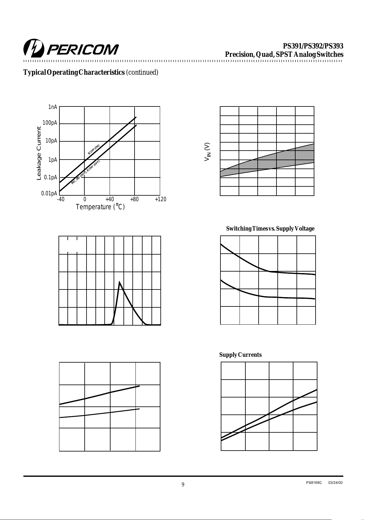
Typical Operating Characteristics (T
A
= + 25ºC, unless otherwise noted)
RON vs. V
COM
& Supply Voltages
Ω
RON vs. V
COM
& Supply Voltages
Ω
RON vs. V
COM
(Single Supply) RON vs. V
COM
and Temperature (Single Supply)
Charge Injection vs. Analog Voltage
Leakage Current vs. V
COM
Page 9
12345678901234567890123456789012123456789012345678901234567890121234567890123456789012345678901212345678901234567890123456789012123456789012
12345678901234567890123456789012123456789012345678901234567890121234567890123456789012345678901212345678901234567890123456789012123456789012
PS391/PS392/PS393
Precision, Quad, SPST Analog Switches
9
PS8168C 03/24/00
Temperature (˚C)
+80 +120+400-40
0.01pA
1nA
100pA
10pA
1pA
0.1pA
I
C
O
M
(O
N
)
I
N
C
, N
O
(O
FF),
I
C
O
M
' (O
FF)
Leakage Current
Typical Operating Characteristics (continued)
Switching Times vs. Supply Voltage
Supply Currents vs. Switching Frequency
V+, V- (±V)
±6 ±7 ±8±5±4±3
0
5
4
3
2
1
02
4
-2
-4 6
0
10
8
6
4
2
I+ (mA)
VIN - Logic Control Voltage (V)
V+ = +5.5V
V- = -5.5V
Supply Current vs. V
IN
V+, V- (±V)
±6 ±7 ±8±5±4±3
0
100
80
60
40
20
t
ON
, t
OFF (ns)
t
OFF
t
ON
Temperature (˚C)
80 1200
0
-40
40
80
60
20
40
Switching Times
t
ON
t
OFF
Switching Times vs. Temperature
Frequency (MHz)
I+, I- (mA)
45321
I+
I-
0
2.5
2
1.5
1
0.5
V+ = +5V
V- = -5V
V
IN
= 5V
P-P
Input Switching Threshold
vs. Supply Voltages
Leakage Current vs. Temperature
Page 10

12345678901234567890123456789012123456789012345678901234567890121234567890123456789012345678901212345678901234567890123456789012123456789012
10
PS8168C 03/24/00
PS391/PS392/PS393
Precision, Quad, SPST Analog Switches
Test Circuits/Timing Diagrams
Figure 1. Switching Time
Figure 2. Break-Before-Make Interval (PS393 only)
Figure 3. Charge Injection
V+
+12V
NO
GND
or NC
COM
V
COM =
+3V(for ton),
-3V(for toff)
Logic
Input
IN
tr <20ns
tf <20ns
V
OUT
= V
COM
R
L
R
L + RON
()
CL INCLUDES FIXTURE AND STRAY CAPACITANCE
V
OUT
R
L
300Ω
C
L
35pF
LOGIC INPUT WAVEFORMS INVERTED FOR
SWITCHES THAT HAVE OPPOSITE LOGIC
t
OFF
t
ON
V
OUT
90%
Logic
Input
Switch
Output
+3V
0V
0V
50%
90%
V+
+5V
NO
GND
-5V
V-
COM
V
COM1
= +3V
IN
RL= 300Ω
C
L
= 35pF
C
L
INCLUDES FIXTURE AND STRAY CAPACITANCE
V
OUT1
R
L2
C
L2
t
D
t
D
90%
90%
V
OUT3
Logic
Input
Switch
Output 1
(V
OUT1
)
+3V
0V
0V
50%
NC
COM
V
COM3
= +3V
Logic
Input
R
L1
C
L1
0V
Switch
Output3
(V
OUT3
)
V+
+5V
NO or
GND
-5V
V-
NC
COM
R
GEN
V
OUT
C
L
1nF
V
OUT
∆V
OUT
IN
V
GEN
ON
ON
OFF
OFF
OFF
OFF
IN
Q = (∆V
OUT
)(CL)
IN
Logic
Input
Page 11

12345678901234567890123456789012123456789012345678901234567890121234567890123456789012345678901212345678901234567890123456789012123456789012
12345678901234567890123456789012123456789012345678901234567890121234567890123456789012345678901212345678901234567890123456789012123456789012
PS391/PS392/PS393
Precision, Quad, SPST Analog Switches
11
PS8168C 03/24/00
Test Circuits/Timing Diagrams (continued)
Figure 4. Off Isolation
Figure 6. Channel-Off Capacitance
Figure 5. Crosstalk
Figure 7. Channel-On Capacitance
V+
+5V
NC
Capacitance
Meter
GND
-5V
V-
or NO
COM
10nF
IN
0V or
2.4V
10nF
f = 1kHz
V+
+5V
NC
Analyzer
GND
-5V
V-
or NO
COM
10nF
IN
R
L
0V or
2.4V
10nF
COM
Signal
Generator 0dBm
V+
+5V
Analyzer
GND
-5V
V-
N02
COM1
10nF
IN2
R
L
10nF
COM
Signal
Generator 0dBm
0V or
2.4V
COM2
IN1
N01
NC
50Ω
0V or
2.4V
V+
+5V
NC
Capacitance
Meter
GND
EN
or NO
COM
10nF
IN
0V or
2.4V
f = 1kHz
As illustrated in Figure 8, PS391 can be used to insert various
capacitors (C1, C2) and set proper RC times for integration. The
resistors R1 and R2 set initial gain. The RIN resistor x C1 or C2 sets
the RC time. The reset switch discharges the hold capacitor
through RIN.
Figure 8. Programmable Integrator and Sample/Hold
Applications
Page 12

12345678901234567890123456789012123456789012345678901234567890121234567890123456789012345678901212345678901234567890123456789012123456789012
12
PS8168C 03/24/00
PS391/PS392/PS393
Precision, Quad, SPST Analog Switches
Ordering InformationOvervoltage Protection
Proper power-supply sequencing is recommended for all CMOS
devices. Do not exceed the absolute maximum ratings, because
stresses beyond the listed ratings may cause permanent damage
to the devices. Always sequence V+ on first, followed by V-, and
then the logic inputs. If power-supply sequencing is not possible,
add two small signal diodes or two current limiting resistors in
series with the supply pins for overvoltage protection (Figure 9).
Adding diodes reduces the analog signal range, but low switch
resistance and low leakage characteristics are unaffected.
Figure 9. Overvoltage protection is accomplished using two
external blocking diodes or two current limiting resistors.
V+
Positive Supply
COMNO
V
g
V-
Pericom Semiconductor Corporation
2380 Bering Drive • San Jose, CA 95131 • 1-800-435-2336 • Fax (408) 435-1100 • http://www.pericom.com
egakcaP
EPC193SPCº07+otCº0PIDPdL61
ESC193SPCº07+otCº0CIOSworraN61
EPE193SPCº58+otCº04-PIDPdL61
ESE193SPCº58+otCº04-CIOSworraN61
QE193SPCº58+otCº04-POSQ61
EPC293SPCº07+otCº0PIDPdL61
ESC293SPCº07+otCº0CIOSworraN61
EPE293SPCº58+otCº04-PIDPdL61
ESE293SPCº58+otCº04-OSworraN61
CI
QE293SPCº58+otCº04-POSQ61
EPC393SPCº07+otCº0PIDPdL61
ESC393SPCº07+otCº0CIOSworraN61
EPE393SPCº58+otCº04-PIDPdL61
ESE393SPCº58+otCº04-OSworraN61
CI
93SP
3
QECº58+otCº04-POSQ61
Part Number
Temperature Range
EEE
EEE
EEE
 Loading...