

Page 1
DATA SHEET
©
PHOTOCOUPLER
PS2801-1,PS2801-4
HIGH ISOLATION VOLTAGE
SOP PHOTOCOUPLER
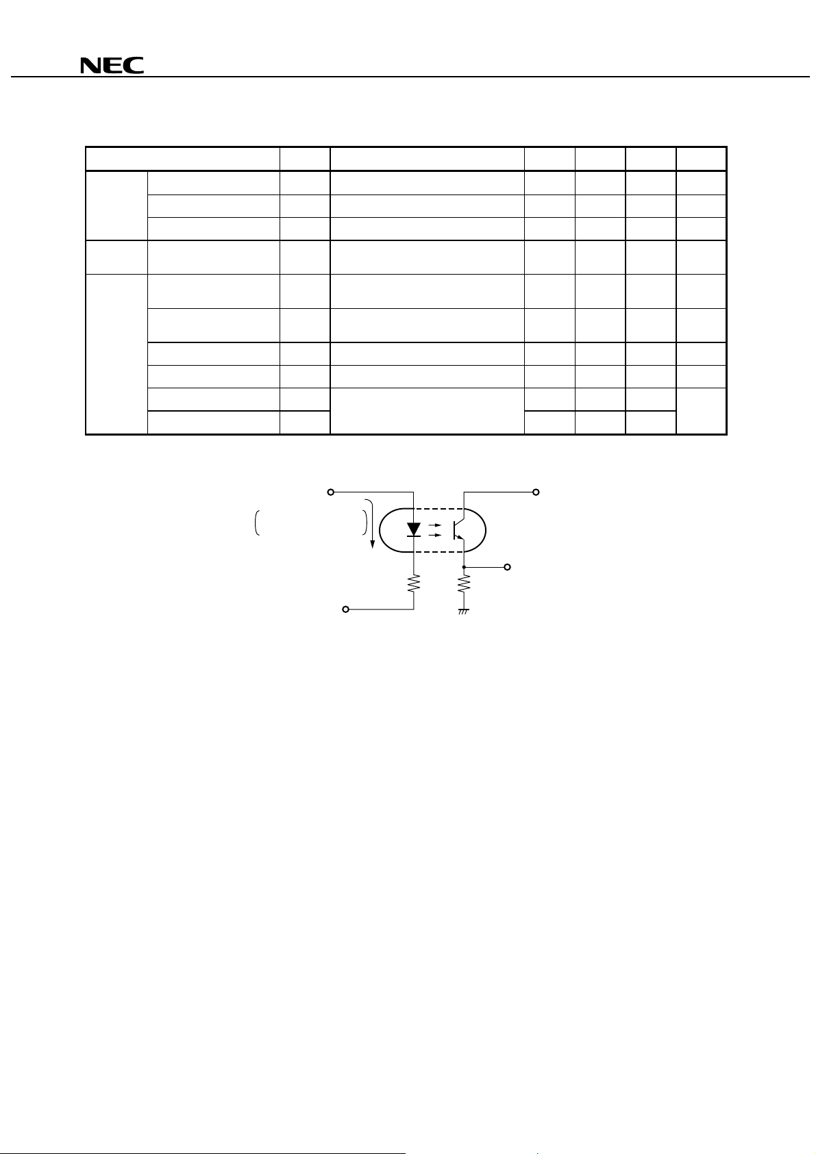
DESCRIPTION
The PS2801-1 and PS2801-4 are optically coupled isolators containing a GaAs light emitting diode and an NPN
silicon phototransistor in a plastic SOP for high density applications.
This package has shield effect to cut off ambient light.
FEATURES
• High isolation voltage (BV = 2 500 Vr.m.s.)
• Small and thin package (4,16-pin SOP, Pin pitch 1.27 mm)
• High collector to emitter voltage (V
• High-speed switching (tr = 3 µs TYP., tf = 5 µs TYP.)
• UL approved: File No. E72422 (S)
• VDE0884 approved (Option): PS2801-4 only
• Operating number of taping product: PS2801-1-F3, F4, PS2801-4-F3, F4
CEO
= 80 V)
NEPOCTM Series
−
−
APPLICATIONS
• Programmable logic controllers
• Measuring instruments
• Power supply
•Hybrid IC
The information in this document is subject to change without notice.
Document No. P12277EJ6V0DS00 (6th edition)
Date Published May 1998 NS CP(K)
Printed in Japan
The mark
••••
shows major revised points.
1991
Page 2
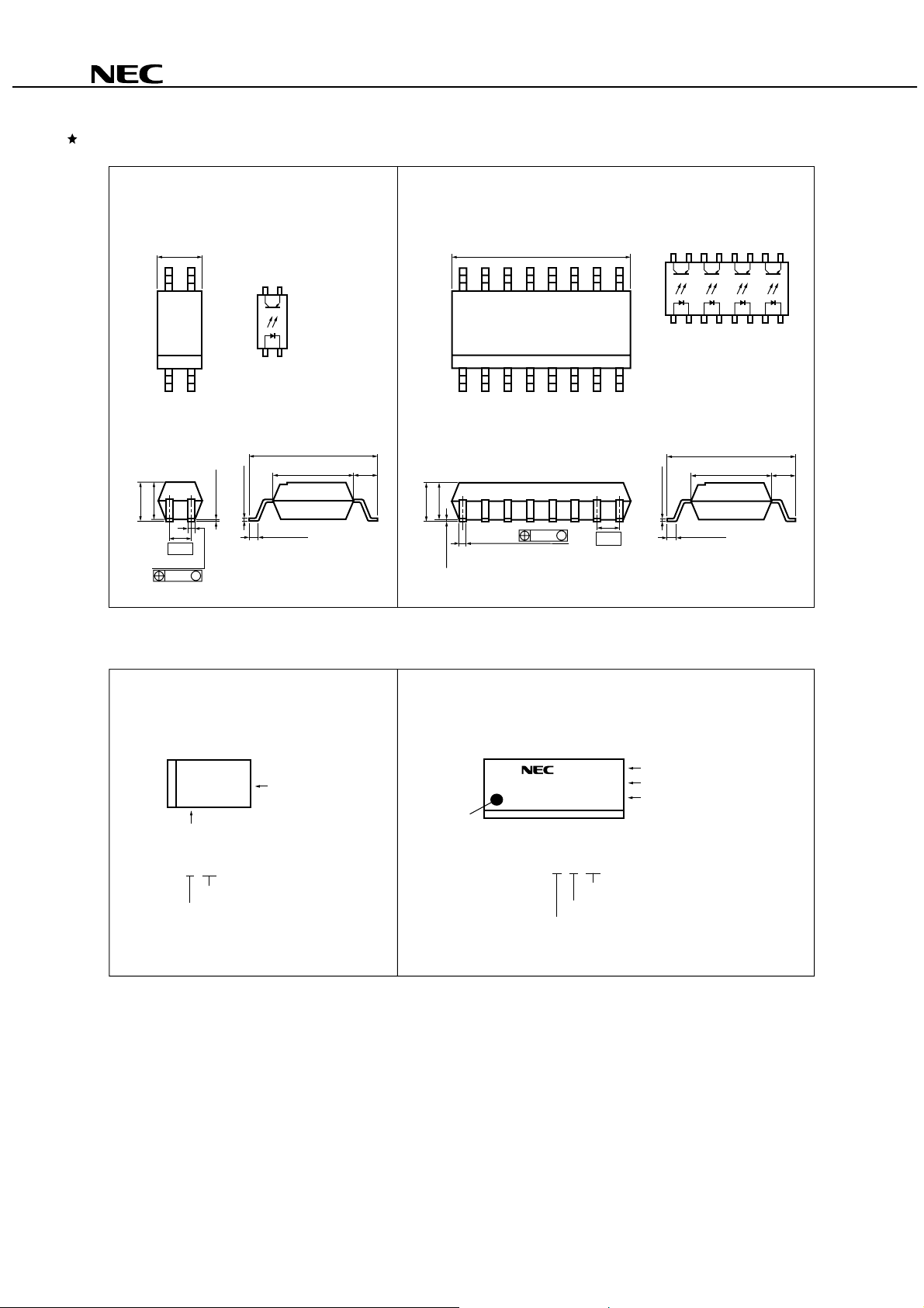
PACKAGE DIMENSIONS (in millimeters)
PS2801-1,PS2801-4
2.0
2.3 MAX.
0.4±0.1
MARKING
2.7±0.3
1.27
0.12
PS2801-1
0.1±0.1
M
–0.05
+0.10
0.15
TOP VIEW
43
12
7.0±0.3
4.4
0.5±0.3
1. Anode
2. Cathode
3. Emitter
4. Collector
1.3
2.0
2.3 MAX.
0.1±0.1
+0.10
–0.05
10.3±0.3
0.12 0.40
PS2801-4
M
1.27
TOP VIEW
161514131211 10 9
12345678
1. 3. 5. 7.
2. 4. 6. 8.
9. 11. 13. 15.
10. 12. 14. 16.
–0.05
+0.10
0.15
0.5±0.3
Anode
Cathode
Emitter
Collector
7.0±0.3
4.4
1.3
PS2801-1
1 503
Last number of type No. : 1
5 03
Weekly Serial Code
Assembly Year
Assembly lot
No. 1 pin
Mark
PS2801-4
JAPAN
PS28012-4
N 503
N 5 03
Weekly Serial Code
Assembly Year
CTR Rank Name
Company & Country Name
Type Number
Assembly lot
2
Page 3

ABSOLUTE MAXIMUM RATINGS (TA = 25 °C, unless otherwise specified)
Parameter Symbol Ratings Unit
PS2801-1 PS2801-4
PS2801-1,PS2801-4
Diode Forward Current (DC) I
Reverse Voltage V
Power Dissipation Derati ng
Power Dissipation P
Peak Forward Current
*1
Transistor Collector to Emitter Voltage V
Emitter to Collector Voltage V
Collector Current I
Power Dissipation Derati ng
Power Dissipation P
Isolation Voltage
*2
Operating Ambient Temperature T
Storage Temperature T
PW = 100
*1
AC voltage for 1 minute at TA = 25 °C, RH = 60 % between input and output
*2
s, Duty Cycle = 1 %
µ
F
R
∆
PD/°C 0.6 0.8 mW/°C
D
FP
I
CEO
ECO
C
∆
PC/°C1.2mW/
C
50 mA
6V
60 80 mW/ch
1A
80 V
6V
50 mA/ch
120 mW/ch
BV 2 500 Vr.m.s.
A
stg
−
55 to +100
−
55 to +150
°
C
°
C
°
C
3
Page 4
ELECTRICAL CHARACTERISTICS (TA = 25 °C)
Parameter Symbol Conditions MIN. TYP. MAX. Unit
PS2801-1,PS2801-4
Diode Forward Voltage V
Reverse Current I
Terminal Capacitance C
Transistor
Collector to Emitter
Dark Current
Coupled
Current Transfer Ratio
C/IF
)
(I
Collector Saturation
CTR I
V
Voltage
Isolation Resistance R
Isolation Capacitance C
Rise Time
Fall Time
Test circuit for switching time
*1
*1
*1
Pulse Input
PW = 100 s
Duty Cycle = 1/10
F
IF = 5 mA 1.1 1.4 V
R
VR = 5 V 5
t
V = 0 V, f = 1.0 MHz 30 pF
CEO
I
VCE = 80 V, IF = 0 mA 100 nA
F
= 5 mA, VCE = 5 V 80 600 %
CE(sat)IF
t
t
= 10 mA, IC = 2 mA 0.3 V
I-O
I-O
V
= 1.0 kV
I-O
V = 0 V, f = 1.0 MHz 0.4 pF
r
VCC = 5 V, IC = 2 mA, RL = 100
f
DC
Ω
10
11
3
5
VCC
µ
F
I
VOUT
50 Ω
RL = 100 Ω
µ
A
Ω
µ
s
4
Page 5

TYPICAL CHARACTERISTICS (TA = 25 °C, unless otherwise specified)
PS2801-1,PS2801-4
DIODE POWER DISSIPATION vs.
AMBIENT TEMPERATURE
100
(mW)
D
75
50
PS2801-1
PS2801-4
0.6 mW/˚C
25
Diode Power Dissipation P
0
25 50
Ambient Temperature T
FORWARD CURRENT vs.
FORWARD VOLTAGE
100
TA = +100 ˚C
50
10
(mA)
F
5
1
0.5
Forward Current I
0.1
+60 ˚C
+25 ˚C
0.8 mW/˚C
75
A
(˚C)
0 ˚C
–25 ˚C
–55 ˚C
100
TRANSISTOR POWER DISSIPATION
vs. AMBIENT TEMPERATURE
200
(mW)
C
150
100
PS2801-1
PS2801-4
1.2 mW/˚C
50
Transistor Power Dissipation P
250
50
Ambient Temperature T
75
A
( ˚C)
COLLECTOR CURRENT vs.
COLLECTOR TO EMITTER VOLTAGE
70
60
50
(mA)
C
40
30
20
Collector Current I
10
50 mA
20 mA
10 mA
IF = 5 mA
100
0.7
0.9 1.1
Forward Voltage V
F
(V)
COLLECTOR TO EMITTER DARK
CURRENT vs. AMBIENT TEMPERATURE
(nA)
10 000
CEO
1 000
100
10
1
Collector to Emitter Dark Current I
–50 –25 0 100
Ambient Temperature T
VCE = 80 V
40 V
24 V
10 V
5 V
25 50
A
(˚C)
75
1.40.8 1.0 1.2 1.3
1.5
0
428610
Collector to Emitter Voltage V
CE
(V)
COLLECTOR CURRENT vs.
COLLECTOR SATURATION VOLTAGE
40
50 mA
20 mA
10
(mA)
C
5
10 mA
5 mA
2 mA
IF = 1 mA
1
0.5
Collector Current I
0.1
0.2 1.00.4 0.6 0.8
0
Collector Saturation Voltage V
CE(sat)
(V)
5
Page 6

PS2801-1,PS2801-4
NORMALIZED CURRENT TRANSFER
RATIO vs. AMBIENT TEMPERATURE
1.2
1.0
0.8
0.6
0.4
Normalized to 1.0
A
= 25 ˚C,
0.2
0.0
Normalized Current Transfer Ratio CTR
–50
–25 25 50
0
Ambient Temperature T
at T
F
= 5 mA, VCE = 5 V
I
A
(˚C)
SWITCHING TIME vs.
LOAD RESISTANCE
100
VCC = 5 V,
50
C
= 2 mA,
I
µ
10
5
CTR = 236 %
t
f
t
t
d
CURRENT TRANSFER RATIO vs.
FORWARD CURRENT
300
V
CE
= 5 V,
n = 3
250
200
150
100
50
Current Transfer Ratio CTR (%)
75
100
0.02 1000.1 1.0 10
Forward Current I
F
(mA)
SWITCHING TIME vs.
LOAD RESISTANCE
1 000
VCC = 5 V,
F
= 5 mA,
I
CTR = 236 %
100
r
µ
10
t
f
t
s
1
Switching Time t ( s)
0.5
0.1
0.01 0.05 0.1
Load Resistance RL (kΩ)
FREQUENCY RESPONSE
0
–5
–10
–15
Normalized Gain Gv
–20
0.5 2 10 20
15 50
0.5
RL = 1 kΩ
Frequency f (kHz)
t
s
15
I
F
= 5 mA,
CE
V
10
= 5 V
100 Ω
300 Ω
200
500
100
1
Switching Time t ( s)
0.1
0.1 1 10 100
L
Load Resistance R
(kΩ)
LONG TERM CTR DEGRADATION
1.2
1.0
2
IF = 5 mA
A
= 25 ˚C
T
F
= 20 mA
I
A
= 25 ˚C
T
F
= 5 mA
I
A
= 60 ˚C
T
3
10
Time (Hr)
10
4
0.8
0.6
0.4
CTR (Relative Value)
0.2
0.0
10
10
t
t
r
d
TYP.
5
10
Remark
6
The graphs indicate nominal characteristics.
Page 7

TAPING SPECIFICATIONS (in millimeters)
PS2801-1
Outline and Dimensions (Tape)
2.0±0.1
4.0±0.1
1.55±0.1
4.0±0.1
1.55±0.1
3.3±0.1
1.75±0.1
7.5±0.1
16.0±0.3
PS2801-1,PS2801-4
2.5±0.1
7.5±0.1
0.3
Tape Direction
PS2801-1-F3 PS2801-1-F4
1
1
1
1
1
104
104
104
104
104
Outline and Dimensions (Reel)
R 1.0
2.0±0.5
13.0±0.5
φ
φ
21.0±0.8
1041104110411041104
1
330
φ
100
φ
Packing: 3 500 pcs/reel
16.4
+2.0
–0.0
7
Page 8

PS2801-4
PS2801-1,PS2801-4
Outline and Dimensions (Tape)
Tape Direction
2.0±0.1
4.0±0.1
1.55±0.1
PS2801-4-F3 PS2801-4-F4
12.0±0.1
1.55±0.1
1.75±0.1
7.5±0.1
16.0±0.3
7.6±0.1
2.5±0.1
10.45±0.1
0.3
Outline and Dimensions (Reel)
R 1.0
Packing: 2 500 pcs/reel
2.0±0.5
13.0±0.5
φ
21.0±0.8
φ
330
φ
100
φ
16.4
+2.0
–0.0
8
Page 9

PS2801-1,PS2801-4
RECOMMENDED SOLDERING CONDITIONS
(1) Infrared reflow soldering
• Peak reflow temperature 235 °C (package surface temperature)
• Time of temperature higher than 210 °C 30 seconds or less
• Number of reflows Three
• Flux Rosin flux containing small amount of chlorine (The flux with a
maximum chlorine content of 0.2 Wt % is recommended.)
Recommended Temperature Profile of Infrared Reflow
(heating)
to 10 s
235 ˚C (peak temperature)
210 ˚C
to 30 s
120 to 160 ˚C
60 to 90 s
(preheating)
Package Surface Temperature T (˚C)
Time (s)
Caution Avoid removing the residual flux with chlorine-based cleaning solvent after a reflow process.
Peak temperature 235 ˚C or below
(2) Dip soldering
• Temperature 260 °C or below (molten solder temperature)
• Time 10 seconds or less
• Number of times One
• Flux Rosin flux containing small amount of chlorine (The flux with a maximum chlorine content of
0.2 Wt % is recommended.)
9
Page 10

PROGRAMMABLE LOGIC CONTROLLERS EXAMPLE
Purpose: In-out interface
PS2801-1,PS2801-4
COM
PS2801–1
PS2801–4
PD4050
Controller
Servo
Motor
Amplifier
Controller
Controller
Pulse Generator
Servo Motor
Driver Unit
Pulse Motor
Driver Unit
Xaxis
Sensor
Motor
Heater
AC.DC
MTGPG
Yaxis
Servo
Motor
M
CRT
PC
Printer
Terminal
Terminal
Printer
FDD
Memory
Cassette
Computer
Programmable Logic
Controller
Power Supply
Controller
10
Page 11

[MEMO]
PS2801-1,PS2801-4
11
Page 12

PS2801-1,PS2801-4
CAUTION
Within this device there exists GaAs (Gallium Arsenide) material which is a
harmful substance if ingested. Please do not under any circumstances break the
hermetic seal.
NEPOC is a trademark of NEC Corporation.
No part of this document may be copied or reproduced in any form or by any means without the prior written
consent of NEC Corporation. NEC Corporation assumes no responsibility for any errors which may appear in this
document.
NEC Corporation does not assume any liability for infringement of patents, copyrights or other intellectual
property rights of third parties by or arising from use of a device described herein or any other liability arising
from use of such device. No license, either express, implied or otherwise, is granted under any patents,
copyrights or other intellectual property rights of NEC Corporation or others.
While NEC Corporation has been making continuous effort to enhance the reliability of its semiconductor devices,
the possibility of defects cannot be eliminated entirely. To minimize risks of damage or injury to persons or
property arising from a defect in an NEC semiconductor device, customers must incorporate sufficient safety
measures in its design, such as redundancy, fire-containment, and anti-failure features.
NEC devices are classified into the following three quality grades:
"Standard", "Special", and "Specific". The Specific quality grade applies only to devices developed based on
a customer designated "quality assurance program" for a specific application. The recommended applications
of a device depend on its quality grade, as indicated below. Customers must check the quality grade of each
device before using it in a particular application.
Standard: Computers, office equipment, communications equipment, test and measurement equipment,
audio and visual equipment, home electronic appliances, machine tools, personal electronic
equipment and industrial robots
Special: Transportation equipment (automobiles, trains, ships, etc.), traffic control systems, anti-disaster
systems, anti-crime systems, safety equipment and medical equipment (not specifically designed
for life support)
Specific: Aircrafts, aerospace equipment, submersible repeaters, nuclear reactor control systems, life
support systems or medical equipment for life support, etc.
The quality grade of NEC devices is "Standard" unless otherwise specified in NEC's Data Sheets or Data Books.
If customers intend to use NEC devices for applications other than those specified for Standard quality grade,
they should contact an NEC sales representative in advance.
Anti-radioactive design is not implemented in this product.
M4 96. 5
 Loading...