

Page 1
DATA SHEET
PHOTOCOUPLER
PS2534-1,-2,-4,PS2534L-1,-2,-4
PS2535-1,-2,-4,PS2535L-1,-2,-4
HIGH COLLECTOR TO EMITTER VOLTAGE
HIGH ISOLATION VOLTAGE
MULTI PHOTOCOUPLER SERIES
DESCRIPTION
The PS2534-1, -2, -4, PS2534L-1, -2, -4, PS2535-1, -2, -4 and PS2535L-1, -2, -4 are optically coupled isolators
containing a GaAs light emitting diode and an NPN silicon darlington connected phototransistor.
The PS2534-1, -2, -4 and PS2535-1, -2, -4 are in a plastic DIP (Dual In-line Package) and the PS2534L-1, -2, -4
and PS2535L-1, -2, -4 are lead bending type (Gull-wing) for surface mount.
FEATURES
• High collector to emitter voltage (V
• High isolation voltage (BV = 5 000 Vr.m.s.)
• High current transfer ratio (CTR = 1 500 % TYP.)
• Ordering number of taping product:PS2534L-1-E3, E4, F3, F4, PS2534L-2-E3, E4
CEO
= 300 V: PS2534-1, -2, -4, PS2534L-1, -2, -4)
CEO
(V
= 350 V: PS2535-1, -2, -4, PS2535L-1, -2, -4)
PS2535L-1-E3, E4, F3, F4, PS2535L-2-E3, E4
−NEPOCTM Series−
APPLICATIONS
• Telephone, Exchange equipment
• FAX/MODEM
The information in this document is subject to change without notice. Before using this document, please
confirm that this is the latest version.
Not all devices/types available in every country. Please check with local NEC representative for
availability and additional information.
Document No. P14066EJ2V0DS00 (2nd edition)
Date Published June 1999 NS CP(K)
Printed in Japan
The mark
••••
shows major revised points.
©
1999
Page 2
PS2534-1,-2,-4,PS2534L-1,-2,-4,PS2535-1,-2,-4,PS2535L-1,-2,-4
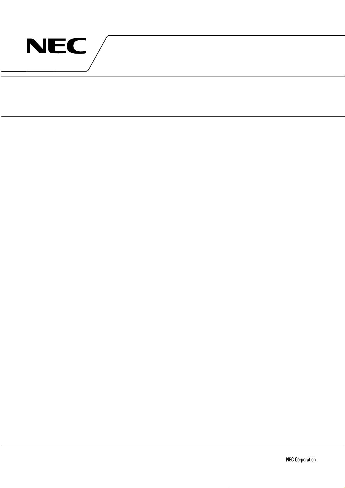
PACKAGE DIMENSIONS (in millimeters)
DIP type
PS2534-2PS2534-1
PS2535-2PS2535-1
–0.5
+0.7
6.5
4.15±0.43.3±0.5
1.25±0.15
3.5±0.3
4.6±0.5
2.54
0.50±0.10
0.25
TOP VIEW
43
12
7.62
0 to 15˚
0.25
M
1. Anode
2. Cathode
3. Emitter
4. Collector
+0.1
–0.05
–0.5
+0.7
6.5
4.15±0.43.3±0.5
1.25±0.15
3.5±0.3
2.54
9.7±0.5
0.50±0.10
0.25
PS2534-4PS2534-1
PS2535-4PS2535-1
TOP VIEW
8765
1234
7.62
0 to 15˚
0.25
–0.05
M
TOP VIEW
16 15 14 13 12 11 10 9
1, 3. Anode
2, 4. Cathode
5, 7. Emitter
6, 8. Collector
+0.1
1.25±0.15
2
–0.5
+0.7
6.5
3.5±0.3
4.15±0.43.2±0.4
4.6±0.35
2.54
0.50±0.10
0.25
TOP VIEW
43
12
7.62
0 to 15˚
0.25
M
1. Anode
2. Cathode
3. Emitter
4. Collector
+0.1
–0.05
–0.5
+0.7
6.5
3.5±0.3
4.15±0.43.3±0.5
1.25±0.15
2.54
Data Sheet P14066EJ2V0DS00
19.8±0.5
0.50±0.10
0.25
12345678
1, 3, 5, 7. Anode
2, 4, 6, 8. Cathode
9, 11, 13, 15. Emitter
10, 12, 14, 16. Collector
7.62
0 to 15˚
M
0.25
+0.1
–0.05
Page 3
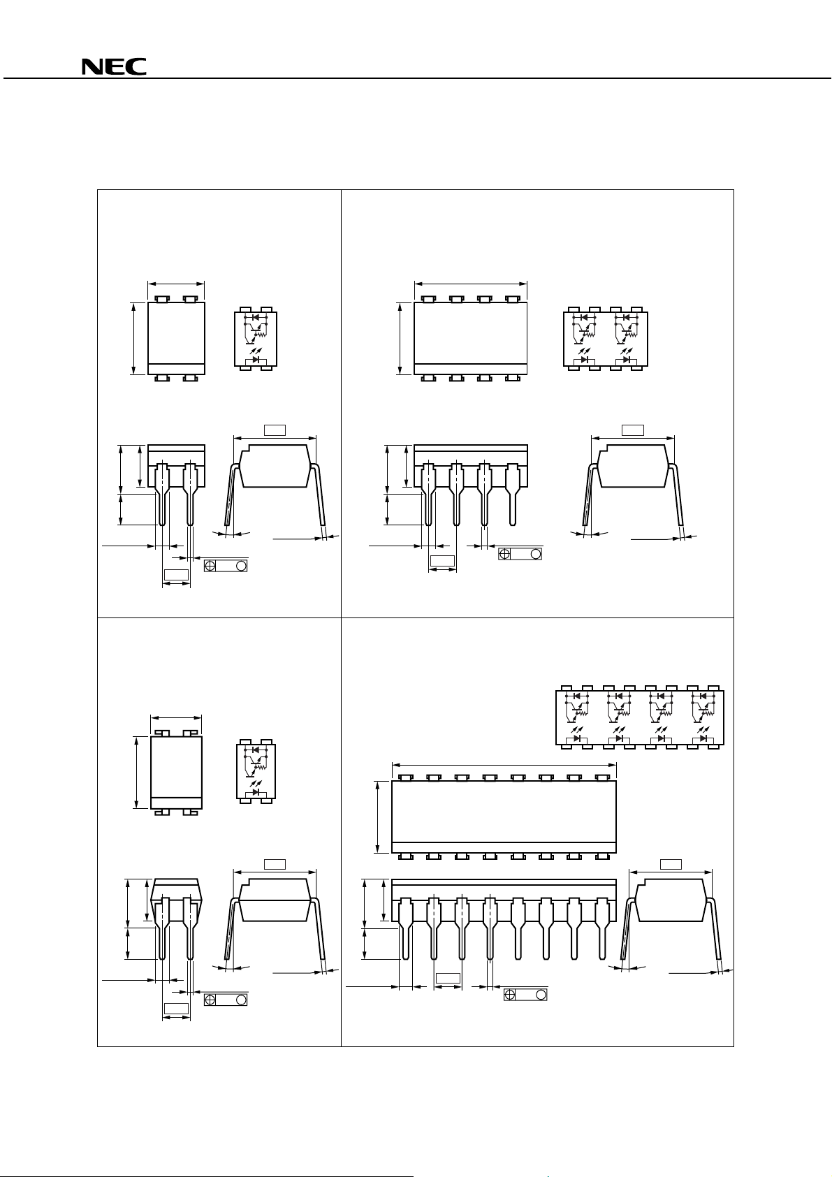
Lead bending type
PS2534-1,-2,-4,PS2534L-1,-2,-4,PS2535-1,-2,-4,PS2535L-1,-2,-4
PS2534L-2PS2534L-1
PS2535L-2PS2535L-1
–0.5
+0.7
6.5
3.5±0.3
1.25±0.15
0.25
2.54
+0.1
0.25
–0.05
43
12
TOP VIEW
1. Anode
2. Cathode
3. Emitter
4. Collector
0.9±0.25
9.60±0.4
0.05 to 0.2
–0.5
+0.7
6.5
1.25±0.15
0.25
3.5±0.3
M
9.7±0.54.6±0.5
2.54
0.15
TOP VIEW
8765
1234
+0.1
–0.05
0.25
0.9±0.25
9.60±0.4
1, 3. Anode
2, 4. Cathode
5, 7. Emitter
6, 8. Collector
0.05 to 0.2
0.15
M
PS2534L-4PS2534L-1
PS2535L-4PS2535L-1
16 15 14 13 12 11 10 9
TOP VIEW
–0.5
+0.7
6.5
3.5±0.3
1.25±0.15
4.6±0.35
2.54
M
0.25
+0.1
0.15
–0.05
0.25
TOP VIEW
43
1. Anode
2. Cathode
3. Emitter
4. Collector
12
0.9±0.25
9.60±0.4
+0.7
0.05 to 0.2
1.25±0.15
–0.5
6.5
3.5±0.3
0.25
19.8±0.5
12345678
1, 3, 5, 7. Anode
2, 4, 6, 8. Cathode
9, 11, 13, 15. Emitter
10, 12, 14, 16. Collector
+0.1
–0.05
0.25
0.05 to 0.2
0.9±0.25
M
2.54
0.15
9.60±0.4
Data Sheet P14066EJ2V0DS00
3
Page 4
PS2534-1,-2,-4,PS2534L-1,-2,-4,PS2535-1,-2,-4,PS2535L-1,-2,-4
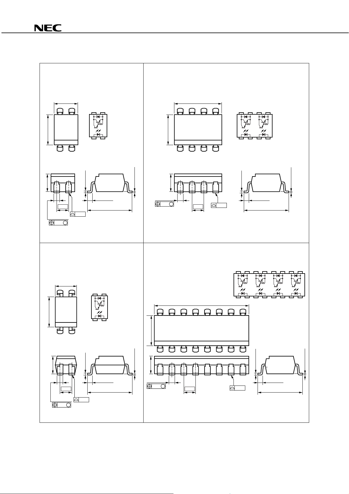
Lead bending type for long distance
PS2534L2-1PS2534L1-1
PS2535L2-1PS2535L1-1
–0.5
+0.7
6.5
3.85±0.43.15±0.35
1.25±0.15
3.5±0.3
4.6±0.35
4.6±0.5
2.54
0.50±0.10
0.25
M
TOP VIEW
43
1. Anode
2. Cathode
3. Emitter
4. Collector
12
10.16
0 to 15˚
0.25
+0.1
–0.05
–0.5
+0.7
6.5
1.25±0.15
0.25
3.5±0.3
M
4.6±0.5
2.54
4.6±0.35
TOP VIEW
43
1. Anode
2. Cathode
3. Emitter
4. Collector
12
10.16
+0.1
–0.05
0.25
0.25±0.2
0.9±0.25
+0.2
11.8
–0.5
0.25
PS2534L2-1PS2534L1-1
PS2535L2-1PS2535L1-1
+0.7
6.5
3.85±0.43.15±0.35
1.25±0.15
–0.5
3.5±0.3
2.54
0.50±0.10
0.25
M
TOP VIEW
43
1. Anode
2. Cathode
3. Emitter
4. Collector
12
10.16
0 to 15˚
0.25
+0.1
–0.05
+0.7
6.5
1.25±0.15
0.25
–0.5
3.5±0.3
M
2.54
0.25
+0.1
0.25
–0.05
TOP VIEW
43
1. Anode
2. Cathode
3. Emitter
4. Collector
12
10.16
0.9±0.25
+0.2
11.8
–0.5
0.25±0.2
4
Data Sheet P14066EJ2V0DS00
Page 5
ORDERING INFORMATION
PS2534-1,-2,-4,PS2534L-1,-2,-4,PS2535-1,-2,-4,PS2535L-1,-2,-4
Part Number Package Packing Style
PS2534-1 4-pin DIP Magazine case 100 pcs PS2534-1
PS2534L-1
PS2534L-1-E3 Embossed Tape 1 000 pcs/reel
PS2534L-1-E4
PS2534L-1-F3 Emboss ed Tape 2 000 pcs/reel
PS2534L-1-F4
PS2534-2 8-pin DIP Magazine case 45 pcs PS2534-2
PS2534L-2
PS2534L-2-E3 Embossed Tape 1 000 pcs/reel
PS2534L-2-E4
PS2534-4 16-pin DIP Magazine case 20 pcs PS2534-4
PS2534L-4
PS2535-1 4-pin DIP Magazine case 100 pcs PS2535-1
PS2535L-1
PS2535L-1-E3 Embossed Tape 1 000 pcs/reel
PS2535L-1-E4
PS2535L-1-F3 Emboss ed Tape 2 000 pcs/reel
PS2535L-1-F4
PS2535-2 8-pin DIP Magazine case 45 pcs PS2535-2
PS2535L-2
PS2535L-2-E3 Embossed Tape 1 000 pcs/reel
PS2535L-2-E4
PS2535-4 16-pin DIP Magazine case 20 pcs PS2535-4
PS2535L-4
Application Part Number
*1
For the application of the Safety Standard, following part number should be used.
*1
Data Sheet P14066EJ2V0DS00
5
Page 6

PS2534-1,-2,-4,PS2534L-1,-2,-4,PS2535-1,-2,-4,PS2535L-1,-2,-4
ABSOLUTE MAXIMUM RATINGS (TA = 25 °°°°C, unless otherwise specified)
Ratings
Parameter Symbol
PS2534-1,
PS2534L-1
PS2534-2, -4,
PS2534L-2, -4
PS2535-1,
PS2535L-1
PS2535-2, -4,
PS2535L-2, -4
Unit
Diode Forward Current (DC) I
Reverse Voltage V
Power Dissipation Derati ng
Power Dissipation P
Peak Forward Current
*1
Transistor Collector to Emitter Voltage V
Emitter to Collector Voltage V
Collector Current I
Power Dissipation Derati ng
Power Dissipation P
Isolation Voltage
*2
Operating Ambient Temperature T
Storage Temperature T
PW = 100
*1
AC voltage for 1 minute at TA = 25 °C, RH = 60 % between input and output
*2
µ
s, Duty Cycle = 1 %
F
R
∆
PD/°C 0.7 0.55 0.7 0.55 mW/°C
D
FP
I
CEO
ECO
C
∆
PC/°C 2.0 1.6 2.0 1.6 mW/°C
C
70 55 70 55 mW/ch
300 350 V
200 160 200 160 mW/ch
BV 5 000 Vr.m.s.
A
stg
50 mA
6V
0.5 A
0.3 V
100 mA/ch
−
55 to +100
−
55 to +150
°
C
°
C
6
Data Sheet P14066EJ2V0DS00
Page 7

PS2534-1,-2,-4,PS2534L-1,-2,-4,PS2535-1,-2,-4,PS2535L-1,-2,-4
ELECTRICAL CHARACTERISTICS (TA = 25 °°°°C)
Parameter Symbol Conditions MIN. TYP. MAX. Unit
Diode Forward Voltage V
Reverse Current I
Terminal Capacitance C
Transistor
Collector to Emitter
Dark Current
Coupled
Current Transfer Ratio
*1
C/IF
(I
)
Collector Saturation
CTR IF = 1 mA, VCE = 2 V 400 1 500 5 500 %
V
Voltage
Isolation Resistance R
Isolation Capacitance C
Rise Time
Fall Time
CTR rank (only PS2534-1, PS2535-1)
*1
*2
*2
N : 400 to 5 500 (%)
L : 1 500 to 5 500 (%)
F
R
t
CEO
I
CE (sat)IF
I-O
I-O
r
t
f
t
IF = 10 mA 1.2 1.4 V
VR = 5 V 5
µ
V = 0 V, f = 1.0 MHz 30 pF
VCE = 300 V, IF = 0 mA 400 nA
= 1 mA, IC = 2 mA 1.0 V
I-O
V
= 1.0 kV
DC
10
11
V = 0 V, f = 1.0 MHz 0.6 pF
VCC = 5 V, IC = 10 mA, RL = 100
Ω
18
µ
5
Test circuit for switching time
*2
Pulse input
I
F
PW = 1 ms,
Duty cycle = 1/10
In monitor
L
= 100 Ω50 Ω
R
A
Ω
s
CC
V
V
OUT
Data Sheet P14066EJ2V0DS00
7
Page 8

PS2534-1,-2,-4,PS2534L-1,-2,-4,PS2535-1,-2,-4,PS2535L-1,-2,-4
TYPICAL CHARACTERISTICS (TA = 25 °°°°C, unless otherwise specified)
DIODE POWER DISSIPATION vs.
AMBIENT TEMPERATURE
100
80
(mW)
D
60
PS2534-2, -4
40
PS2535-2, -4
20
Diode Power Dissipation P
0
PS2534-1
PS2535-1
25
0.7 mW/˚C
0.55 mW/˚C
50
FORWARD CURRENT vs.
FORWARD VOLTAGE
100
TA = +100 ˚C
50
+60 ˚C
+25 ˚C
10
(mA)
F
5
1
0.5
Forward Current I
0.1
0.7 0.9 1.1 1.3 1.50.8 1.0 1.2 1.4
Forward Voltage VF (V)
75
0 ˚C
–25 ˚C
–50 ˚C
100
TRANSISTOR POWER DISSIPATION vs.
AMBIENT TEMPERATURE
240
220
200
(mW)
C
180
160
140
120
100
Transistor Power Dissipation P
PS2534-2, -4
PS2535-2, -4
80
60
40
20
0
Ambient Temperature TA (˚C)Ambient Temperature TA (˚C)
PS2534-1
PS2535-1
1.6 mW/˚C
25 50
2.0 mW/˚C
75
COLLECTOR CURRENT vs.
COLLECTOR SATURATION VOLTAGE
100
50
(mA)
C
10
5
Collector Current I
1
0.4 0.6 0.8 1.0
Collector Saturation Voltage V
IF = 0.5 mA
1.2
1.4 1.6
CE(sat)
(V)
100
5 mA
3 mA
2 mA
1 mA
COLLECTOR TO EMITTER DARK
CURRENT vs. AMBIENT TEMPERATURE
100 000
(nA)
CEO
10 000
1 000
Collector to Emitter Dark Current I
100
10
1
–50
CEO
= 300 V
V
CTR = 1 068 %
2 290 %
4 360 %
–25
0
Ambient Temperature TA (˚C)
25
50
8
75 100
Data Sheet P14066EJ2V0DS00
COLLECTOR CURRENT vs.
COLLECTOR TO EMITTER VOLTAGE
100
50
(mA)
C
10
Collector Current I
5 mA
5
1
0
1234
Collector to Emitter Voltage VCE (V)
3 mA
2 mA
IF = 0.5 mA
1 mA
5
Page 9

PS2534-1,-2,-4,PS2534L-1,-2,-4,PS2535-1,-2,-4,PS2535L-1,-2,-4
NORMALIZED CURRENT TRANSFER
RATIO vs. AMBIENT TEMPERTURE
1.4
1.2
1.0
0.8
0.6
0.4
0.2
Normalized Current Transfer Ratio CTR
0.0
–50
–25
0
Ambient Temperature TA (˚C)
Normalized to 1.0
A
= 25 ˚C,
at T
F
= 1 mA, VCE = 2 V
I
25
50
SWITCHING TIME vs.
LORD RESISTANCE
1 000
VCC = 10 V,
C
= 10 mA,
I
CTR = 1 800 %
100
µ
10
1
Switching Time t ( s)
75
CURRENT TRANSFER RATIO vs.
FORWARD CURRENT
100
4 500
4 000
3 500
3 000
2 500
2 000
1 500
1 000
500
Current Transfer Ratio CTR (%)
0
0.1
0.5
1
Forword Current IF (mA)
VCE = 2 V
105
40
LONG TERM CTR DEGRADATION
1.2
IF = 1 mA
t
r
t
f
t
d
t
s
1.0
0.8
0.6
0.4
CTR (Relative Value)
0.2
TA = 25 ˚C
TA = 60 ˚C
0.1
10
Remark
50
100 500 1000
Load Resistance RL (Ω)
The graphs indicate nominal characteristics.
0.0
10 10
2
10
3
10
4
10
5
10
6
Time (Hr)
Data Sheet P14066EJ2V0DS00
9
Page 10

PS2534-1,-2,-4,PS2534L-1,-2,-4,PS2535-1,-2,-4,PS2535L-1,-2,-4
TAPING SPECIFICATIONS (in millimeters)
Outline and Dimensions (Tape)
2.0±0.1
4.0±0.1
1.55±0.1
8.0±0.1
1.55±0.1
5.6±0.1
1.75±0.1
7.5±0.1
16.0±0.3
4.3±0.2
10.3±0.1
0.3
Tape Direction
PS2534L-1-E3
PS2535L-1-E3
Outline and Dimensions (Reel)
R 1.0
2.0±0.5
φ
13.0±0.5
φ
21.0±0.8
PS2534L-1-E4
PS2535L-1-E4
250
φ
80.0±5.0
φ
1.6
10
Packing: 1 000 pcs/reel
Data Sheet P14066EJ2V0DS00
16.4
+2.0
–0.0
Page 11

PS2534-1,-2,-4,PS2534L-1,-2,-4,PS2535-1,-2,-4,PS2535L-1,-2,-4
Outline and Dimensions (Tape)
2.0±0.1
4.0±0.1
1.55±0.1
8.0±0.1
Tape Direction
1.55±0.1
5.6±0.1
1.75±0.1
7.5±0.1
16.0±0.3
4.3±0.2
10.3±0.1
0.3
PS2534L-1-F3
PS2535L-1-F3
Outline and Dimensions (Reel)
R 1.0
2.0±0.5
φ
13.0±0.5
φ
21.0±0.8
PS2534L-1-F4
PS2535L-1-F4
330
φ
80.0±5.0
φ
1.5
Packing: 2 000 pcs/reel
Data Sheet P14066EJ2V0DS00
16.4
+2.0
–0.0
11
Page 12

PS2534-1,-2,-4,PS2534L-1,-2,-4,PS2535-1,-2,-4,PS2535L-1,-2,-4
Outline and Dimensions (Tape)
2.0±0.1
4.0±0.1
1.55±0.1
12.0±0.1
Tape Direction
1.55±0.1
10.4±0.1
1.75±0.1
7.5±0.1
16.0±0.3
4.3±0.2
10.3±0.1
0.3
PS2534L-2-E3
PS2535L-2-E3
Outline and Dimensions (Reel)
R 1.0
2.0±0.5
13.0±0.5
φ
21.0±0.8
φ
PS2534L-2-E4
PS2535L-2-E4
330
φ
80.0±5.0
φ
1.5
12
Packing: 1 000 pcs/reel
Data Sheet P14066EJ2V0DS00
16.4
+2.0
–0.0
Page 13

PS2534-1,-2,-4,PS2534L-1,-2,-4,PS2535-1,-2,-4,PS2535L-1,-2,-4
RECOMMENDED SOLDERING CONDITIONS
(1) Infrared reflow soldering
• Peak reflow temperature 235 °C (package surface temperature)
• Time of temperature higher than 210 °C 30 seconds or less
• Number of reflows Three
• Flux Rosin flux containing small amount of chlorine (The flux with a
maximum chlorine content of 0.2 Wt % is recommended.)
Recommended Temperature Profile of Infrared Reflow
(heating)
to 10 s
235 ˚C (peak temperature)
210 ˚C
to 30 s
120 to 160 ˚C
60 to 90 s
(preheating)
Package Surface Temperature T (˚C)
Time (s)
(2) Dip soldering
• Temperature 260 °C or below (molten solder temperature)
• Time 10 seconds or less
• Number of times One
• Flux Rosin flux containing small amount of chlorine (The flux with a maximum chlorine content of
0.2 Wt % is recommended.)
(3) Cautions
•Fluxes
Avoid removing the residual flux with freon-based and chlorine-based cleaning solvent.
Data Sheet P14066EJ2V0DS00
13
Page 14

[MEMO]
PS2534-1,-2,-4,PS2534L-1,-2,-4,PS2535-1,-2,-4,PS2535L-1,-2,-4
14
Data Sheet P14066EJ2V0DS00
Page 15

[MEMO]
PS2534-1,-2,-4,PS2534L-1,-2,-4,PS2535-1,-2,-4,PS2535L-1,-2,-4
Data Sheet P14066EJ2V0DS00
15
Page 16

PS2534-1,-2,-4,PS2534L-1,-2,-4,PS2535-1,-2,-4,PS2535L-1,-2,-4
CAUTION
Within this device there exists GaAs (Gallium Arsenide) material which is a
harmful substance if ingested. Please do not under any circumstances break the
hermetic seal.
NEPOC is a trademark of NEC Corporation.
• The information in this document is subject to change without notice. Before using this document, please
confirm that this is the latest version.
• No part of this document may be copied or reproduced in any form or by any means without the prior written
consent of NEC Corporation. NEC Corporation assumes no responsibility for any errors which may appear in
this document.
• NEC Corporation does not assume any liability for infringement of patents, copyrights or other intellectual property
rights of third parties by or arising from use of a device described herein or any other liability arising from use
of such device. No license, either express, implied or otherwise, is granted under any patents, copyrights or other
intellectual property rights of NEC Corporation or others.
• Descriptions of circuits, software, and other related information in this document are provided for illustrative
purposes in semiconductor product operation and application examples. The incorporation of these circuits,
software, and information in the design of the customer's equipment shall be done under the full responsibility
of the customer. NEC Corporation assumes no responsibility for any losses incurred by the customer or third
parties arising from the use of these circuits, software, and information.
• While NEC Corporation has been making continuous effort to enhance the reliability of its semiconductor devices,
the possibility of defects cannot be eliminated entirely. To minimize risks of damage or injury to persons or
property arising from a defect in an NEC semiconductor device, customers must incorporate sufficient safety
measures in its design, such as redundancy, fire-containment, and anti-failure features.
• NEC devices are classified into the following three quality grades:
"Standard", "Special", and "Specific". The Specific quality grade applies only to devices developed based on a
customer designated "quality assurance program" for a specific application. The recommended applications of
a device depend on its quality grade, as indicated below. Customers must check the quality grade of each device
before using it in a particular application.
Standard: Computers, office equipment, communications equipment, test and measurement equipment,
audio and visual equipment, home electronic appliances, machine tools, personal electronic
equipment and industrial robots
Special: Transportation equipment (automobiles, trains, ships, etc.), traffic control systems, anti-disaster
systems, anti-crime systems, safety equipment and medical equipment (not specifically designed
for life support)
Specific: Aircraft, aerospace equipment, submersible repeaters, nuclear reactor control systems, life
support systems or medical equipment for life support, etc.
The quality grade of NEC devices is "Standard" unless otherwise specified in NEC's Data Sheets or Data Books.
If customers intend to use NEC devices for applications other than those specified for Standard quality grade,
they should contact an NEC sales representative in advance.
M7 98. 8
 Loading...