

现货库存、技术资料、百科信息、热点资讯,精彩尽在鼎好!
PROFET
Smart Highside Power Switch
Features
1
•
Load dump and reverse battery protection
•
Clamp of negative voltage at output
•
Short-circuit protection
•
Current limitation
•
Thermal shutdown
•
Diagnostic feedback
•
Open load detection in ON-state
•
CMOS compatible input
•
Electrostatic discharge (ESD) protection
•
Loss of ground and loss of V
•
Overvoltage protection
•
Undervoltage and overvoltage shutdown with auto-
protection2)
bb
)
restart and hysteresis
Application
•
µC compatible power switch with diagnostic feedback
for 12 V and 24 V DC grounded loads
•
All types of resistive, inductive and capacitve loads
•
Replaces electromechanical relays and discrete circuits
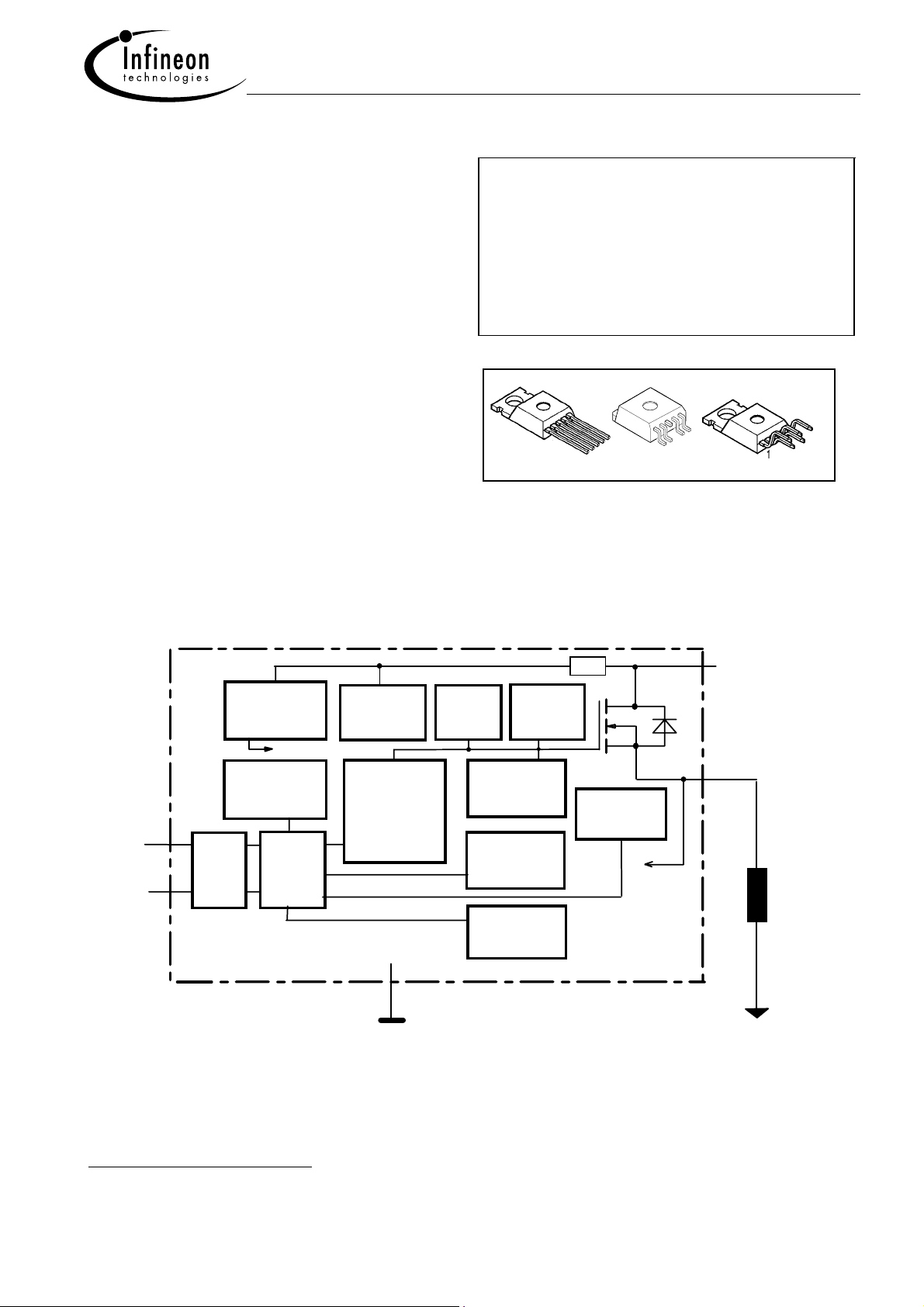
Product Summary
V
Load dump
Vbb-V
V
bb (operation)
V
bb (reverse)
80 V
Avalanche Clamp 58 V
OUT
4.5 ... 42 V
-32 V
RON 38
I
L(SCp)
I
L(SCr)
I
L(ISO)
44 A
35 A
11 A
5
Straight leads
1
SMD
®
BTS 432 E2
mΩ
5
5
1
Standard
General Description
N channel vertical power FET with charge pump, ground referenced CMOS compatible input and diagnostic
feedback, integrated in Smart SIPMOS
Voltage
source
V
Logic
Voltage
sensor
IN
2
ESD
4
ST
Logic
chip on chip technology. Providing protective functions.
+ V
bb
PROFET
bb
OUT
Overvoltage
protection
Charge pump
Level shifter
Rectifier
GND
Current
limit
Gate
protection
Limit for
unclamped
ind. loads
Open load
detection
Short circuit
detection
R
Temperature
sensor
1
Signal GND
Load GND
3
5
Load
1)
No external components required, reverse load current limited by connected load.
2)
Additional external diode required for charged inductive loads
Semiconductor Group 1 of 14 2003-Oct-01
BTS 432 E2
Pin Symbol Function
1 GND - Logic ground
2 IN I Input, activates the power switch in case of logical high signal
3 Vbb + Positive power supply voltage,
the tab is shorted to this pin
4 ST S Diagnostic feedback, low on failure
5 OUT
O Output to the load
(Load, L)
Maximum Ratings at Tj = 25 °C unless otherwise specified
Parameter Symbol Values Unit
Supply voltage (overvoltage protection see page 3) Vbb 63 V
3
Load dump protection V
LoadDump
= UA + Vs, UA = 13.5 V
)
V
66.5 V
s
RI= 2 Ω, RL= 1.1 Ω, td= 200 ms, IN= low or high
Load current (Short-circuit current, see page 4) IL self-limited A
Operating temperature range
Storage temperature range
Power dissipation (DC) P
Tj
T
stg
125 W
tot
-40 ...+150
-55 ...+150
°C
Inductive load switch-off energy dissipation,
single pulse Tj=150 °C: EAS 1.7 J
Electrostatic discharge capability (ESD)
V
2.0 kV
ESD
(Human Body Model)
Input voltage (DC) VIN -0.5 ... +6 V
Current through input pin (DC)
Current through status pin (DC)
see internal circuit diagrams page 6...
Thermal resistance chip - case:
junction - ambient (free air):
IIN
IST
R
thJC
R
thJA
±5.0
mA
±5.0
≤ 1
≤ 75
K/W
SMD version, device on pcb4): ≤ tbd
3)
VS is setup without DUT connected to the generator per ISO 7637-1 and DIN 40839
4)
Device on 50mm*50mm*1.5mm epoxy PCB FR4 with 6cm
connection. PCB is vertical without blown air.
2
(one layer, 70µm thick) copper area for Vbb
Semiconductor Group 2 2003-Oct-01

BTS 432 E2
Electrical Characteristics
Parameter and Conditions Symbol Values Unit
at Tj = 25 °C, Vbb = 12 V unless otherwise specified
Load Switching Capabilities and Characteristics
min typ max
On-state resistance (pin 3 to 5)
IL = 2 A Tj=25 °C:
RON
--
Tj=150 °C:
Nominal load current (pin 3 to 5)
I
9 11 -- A
L(ISO)
ISO Proposal: VON = 0.5 V, TC = 85 °C
Output current (pin 5) while GND disconnected or
I
L(GNDhigh)
-- -- 1 mA
GND pulled up, VIN= 0, see diagram page 7,
Tj =-40...+150°C
Turn-on time to 90% V
Turn-off time to 10% V
R
= 12 Ω, Tj =-40...+150°C
L
Slew rate on
10 to 30% V
OUT
, R
= 12 Ω, Tj =-40...+150°C
L
Slew rate off
70 to 40% V
, RL = 12 Ω, Tj =-40...+150°C
OUT
OUT
OUT
:
ton
:
t
off
dV /dton 0.4 -- 2.5 V/µs
-dV/dt
1 -- 5 V/µs
off
50
10
Operating Parameters
Operating voltage 5) Tj =-40...+150°C: V
Undervoltage shutdown Tj =-40...+150°C: V
Undervoltage restart Tj =-40...+150°C: V
Undervoltage restart of charge pump
V
4.5 -- 42 V
bb(on)
bb(under)
bb(u rst)
bb(ucp)
2.4 -- 4.5 V
-- -- 4.5 V
-- 6.5 7.5 V
see diagram page 12 Tj =-40...+150°C:
Undervoltage hysteresis
∆V
bb(under)
= V
bb(u rst)
- V
bb(under)
Overvoltage shutdown Tj =-40...+150°C: V
Overvoltage restart Tj =-40...+150°C: V
Overvoltage hysteresis Tj =-40...+150°C: ∆V
Overvoltage protection
6)
Tj =-40°C:
Ibb=40 mA Tj =25...+150°C:
Standby current (pin 3) Tj=-40...+25°C:
VIN=0 T
Leakage output current (included in I
VIN=0
bb(off)
=150°C:
j
)
Operating current (Pin 1)7), VIN=5 V
∆V
bb(over)
bb(o rst)
V
bb(AZ)
bb(under)
bb(over)
-- 0.2 -- V
42 -- 52 V
42 -- -- V
-- 0.2 -- V
60
63
I
--
bb(off)
--
I
-- 6 -- µA
L(off)
I
-- 1.1 -- mA
GND
30
55
160
--
--
67
12
18
38
mΩ
70
300
µs
80
-- V
25
µA
60
5)
At supply voltage increase up to V
6)
see also V
7)
Add I
, if IST > 0, add IIN, if VIN>5.5 V
ST
in table of protection functions and circuit diagram page 7. Meassured without load.
ON(CL)
= 6.5 V typ without charge pump, V
bb
≈Vbb - 2 V
OUT
Semiconductor Group 3 2003-Oct-01
BTS 432 E2
Parameter and Conditions Symbol Values Unit
at Tj = 25 °C, Vbb = 12 V unless otherwise specified
min typ max
Protection Functions8)
Initial peak short circuit current limit (pin 3 to 5)9),
( max 400 µs if VON > V
ON(SC)
)
=-40°C:
Tj
=25°C:
Tj
=+150°C:
Tj
Repetitive short circuit current limit I
I
--
L(SCp)
--
--
24
L(SCr)
44
--
Tj = Tjt (see timing diagrams, page 10) 22 35 -- A
Short circuit shutdown delay after input pos. slope
> V
V
ON
min value valid only, if input "low" time exceeds 30 µs
, Tj =-40..+150°C:
ON(SC)
Output clamp (inductive load switch off)
at V
= Vbb - V
OUT
ON(CL)
IL= 30 mA
,
t
V
Short circuit shutdown detection voltage
(pin 3 to 5) V
d(SC)
ON(CL)
ON(SC)
80
--
--
-- 400 µs
58 -- V
8.3 -- V
Thermal overload trip temperature Tjt 150 -- -- °C
Thermal hysteresis
Inductive load switch-off energy dissipation
T
= 150 °C, single pulse Vbb = 12 V:
j Start
10)
,
Vbb = 24 V:
Reverse battery (pin 3 to 1)
11)
-Vbb -- -- 32 V
∆
Tjt -- 10 -- K
E
AS
E
Load12
E
Load24
-- -- 1.7
Integrated resistor in Vbb line Rbb -- 120 -- Ω
Diagnostic Characteristics
Open load detection current Tj=-40 °C:
(on-condition) Tj=25..150°C:
I
2
L (OL)
2
--
--
74
1.3
1.0
900
750
A
--
--
J
mA
8)
Integrated protection functions are designed to prevent IC destruction under fault conditions described in the
data sheet. Fault conditions are considered as "outside" normal operating range. Protection functions are not
designed for continuous repetitive operation.
9)
Short circuit current limit for max. duration of 400 µs, prior to shutdown (see t
10)
While demagnetizing load inductance, dissipated energy in PROFET is EAS= V
V
2
= 1/
E
AS
11)
Reverse load current (through intrinsic drain-source diode) is normally limited by the connected load.
Reverse current I
these condition is dependent on the size of the heatsink. Reverse I
external GND-resistor (150 Ω). Input and Status currents have to be limited (see max. ratings page 2 and
circuit page 7).
* L * I
2
* (
L
V
ON(CL)
of ≈ 0.3 A at Vbb= -32 V through the logic heats up the device. Time allowed under
GND
ON(CL)
- V
), see diagram page 8
bb
page 4)
d(SC)
* iL(t) dt, approx.
ON(CL)
can be reduced by an additional
GND
Semiconductor Group 4 2003-Oct-01
BTS 432 E2
Parameter and Conditions Symbol Values Unit
at Tj = 25 °C, Vbb = 12 V unless otherwise specified
Input and Status Feedback
12)
Input turn-on threshold voltage
T
=-40..+150°C:
j
Input turn-off threshold voltage
T
=-40..+150°C:
j
V
IN(T+)
V
IN(T-)
Input threshold hysteresis ∆ V
Off state input current (pin 2) VIN = 0.4 V: I
On state input current (pin 2) VIN = 3.5 V: I
Status invalid after positive input slope
(short circuit) Tj=-40 ... +150°C:
Status invalid after positive input slope
(open load) Tj=-40 ... +150°C:
IN(off)
IN(on)
t
d(ST SC)
t
d(ST)
min typ max
1.5 -- 2.4 V
1.0 -- -- V
-- 0.5 -- V
IN(T)
1 -- 30 µA
10 25 50 µA
80 200 400 µs
350 -- 1600 µs
Status output (open drain)
Zener limit voltage Tj =-40...+150°C, IST = +1.6 mA:
ST low voltage Tj =-40...+150°C, IST = +1.6 mA:
V
ST(high)
V
ST(low)
5.4
--
6.1
--
0.4
--
V
12)
If a ground resistor R
is used, add the voltage drop across this resistor.
GND
Semiconductor Group 5 2003-Oct-01

BTS 432 E2
Truth Table
Normal
operation
Input- Output Status
level 432
level
L
H
Open load L
H
Short circuit
to GND
Short circuit
to V
bb
Overtemperature
Undervoltage
L
H
L
H
L
H
L
H
Overvoltage L H L
L = "Low" Level
H = "High" Level
13
L
H
H
L
L
H
H
L
L
L
L
L
)
D2
H
H
H
L
H
L
H
14)
H (L
)
L
L
15)
L
15)
L
L
L
432
E2/F2
H
H
H
L
H
L
H
H (L
L
L
H
H
H
H
14)
432
I2
H
H
L
H
H
L
L
)
H
L
L
15)
L
15)
L
L
L
Terms
V
bb
Input circuit (ESD protection)
I
bb
R
GND
3
V
bb
PROFET
GND
1
I
GND
OUT
I
V
L
5
V
ON
OUT
ZD
I1
continuous current
I
IN
IN
2
I
ST
ST
V
IN
4
V
ST
IN
6.1 V typ., ESD zener diodes are not designed for
R
I
ESD-
ZD ZD
I1 I2
GND
I
I
13)
Power Transistor off, high impedance
14)
Low resistance short V
15)
No current sink capability during undervoltage shutdown
to output may be detected by no-load-detection
bb
Semiconductor Group 6 2003-Oct-01

BTS 432 E2
Status output
R
ST(ON)
+5V
ST
Overvolt. and reverse batt. protection
R
bb
V
R
IN
IN
Z
+ V
bb
ESD-
GND
ZD
ESD-Zener diode: 6.1 V typ., max 5 mA;
R
ST(ON)
< 250 Ω at 1.6 mA, ESD zener diodes are not
designed for continuous current
Short Circuit detection
Fault Condition: VON > 8.3 V typ.; IN high
+ V
bb
V
ON
OUT
Logic
unit
Inductive and overvoltage output clamp
Short circuit
detection
V
Z
+ V
bb
V
ON
Logic
ST
R
ST
R
= 120 Ω typ., VZ +Rbb*40 mA = 67 V typ., add
R
bb
, RIN, RST for extended protection
R
GND
GND
GND
Signal GND
PROFET
Open-load detection
ON-state diagnostic condition: VON < R
high
ON
Logic
unit
Open load
detection
GND disconnect
ON
* I
L(OL)
+ V
OUT
V
bb
; IN
ON
V
OUT
GND
VON clamped to 58 V typ.
OUT
V
V
bb
V
IN
ST
IN
2
ST
4
Any kind of load. In case of Input=high is V
Due to V
>0, no VST = low signal available.
GND
3
V
bb
PROFET
GND
1
V
GND
OUT
OUT
5
≈ VIN - V
IN(T+)
.
Semiconductor Group 7 2003-Oct-01

BTS 432 E2
GND disconnect with GND pull up
3
V
PROFET
- V
IN
bb
GND
1
V
GND
device stays off
IN(T+)
OUT
5
V
bb
V
IN
Any kind of load. If V
Due to V
>0, no VST = low signal available.
GND
2
V
4
ST
GND
IN
ST
> V
Vbb disconnect with charged inductive
load
3
high
V
bb
IN
2
ST
4
V
bb
PROFET
GND
1
OUT
5
3
high
IN
2
ST
4
V
bb
Inductive Load switch-off energy
V
bb
PROFET
GND
1
OUT
dissipation
E
bb
V
PROFET
GND
* L * I
bb
OUT
= Ebb + EL - ER.
AS
2
L
IN
=
ST
Energy dissipated in PROFET E
1
< EL, EL =
E
Load
/
2
5
E
AS
E
Load
E
L
E
R
Semiconductor Group 8 2003-Oct-01

BTS 432 E2
Options Overview
all versions: High-side switch, Input protection, ESD protection, load dump and
reverse battery protection , protection against loss of ground
Type BTS
Logic version
432D2 432E2 432F2 432I2
D E F I
Overtemperature protection
16)17
Tj >150 °C, latch function
Tj >150 °C, with auto-restart on cooling
)
X
X X
X
Short-circuit to GND protection
switches off when VON>8.3 V typ.
(when first turned on after approx. 200 µs)
16)
X X X X
Open load detection
in OFF-state with sensing current 30 µA typ.
in ON-state with sensing voltage drop across
power transistor
Undervoltage shutdown with auto restart
Overvoltage shutdown with auto restart
X
X X X X
X X X X
X
X
Status feedback for
overtemperature
short circuit to GND
short to V
open load
undervoltage
overvoltage
bb
-
X
X
18)
X
X
X
X
X
18)
X
-
-
X
X
18)
X
-
-
Status output type
CMOS
Open drain
Output negative voltage transient limit
X
X
X
(fast inductive load switch off)
to Vbb - V
ON(CL)
X X X X
Load current limit
high level (can handle loads with high inrush currents)
medium level
low level
16)
17)
18)
(better protection of applic ation)
Latch except when V
0 V only if forced externally). So the device remains latched unless V
between turn on and t
With latch function. Reseted by a) Input low, b) Undervoltage, c) Overvoltage
Low resistance short V
bb -VOUT
d(SC)
bb
< V
ON(SC)
.
to output may be detected by no-load-detection
after shutdown. In most cases V
X X
X
OUT
< V
bb
X
X
X
X
X
X
X
X
X
= 0 V after shutdown (V
ON(SC)
(see page 4). No latch
OUT
≠
Semiconductor Group 9 2003-Oct-01

BTS 432 E2
Timing diagrams
Figure 1a: Vbb turn on:
Figure 2b: Switching an inductive load
IN
t
V
V
bb
OUT
d(bb IN)
A
ST open drain
A
in case of too early VIN=high the device may not turn on (curve A)
t
approx. 150 µs
d(bb IN)
IN
d(ST)
t
ST
*)
V
OUT
I
L
I
L(OL)
t
*) if the time constant of load is too large, open-load-status may
occur
t
Figure 2a: Switching a lamp,
IN
ST
V
OUT
I
L
Figure 3a: Turn on into short circuit,
IN
ST
V
OUT
t
d(SC)
I
L
t
t
approx. 200µs if Vbb - V
d(SC)
> 8.3 V typ.
OUT
t
Semiconductor Group 10 2003-Oct-01

BTS 432 E2
Figure 3b: Turn on into overload,
IN
I
L
I
L(SCp)
I
L(SCr)
Figure 4a: Overtemperature:
Reset if T
<Tjt
j
IN
ST
V
OUT
T
J
ST
Heating up may require several milliseconds , Vbb - V
typ.
Figure 3c: Short circuit while on:
IN
ST
V
OUT
OUT
< 8.3 V
t
Figure 5a: Open load: detection in ON-state, turn
on/off to open load
IN
t
ST
d(ST)
V
OUT
t
I
L
I
L
**)
t
open
t
**) current peak approx. 20 µs
Semiconductor Group 11 2003-Oct-01

BTS 432 E2
Figure 5b: Open load: detection in ON-state, open
load occurs in on-state
IN
Figure 6b:
VON [V]
V
Undervoltage restart of charge pump
on
V
ON(CL)
off
t
d(ST OL1)
ST
V
OUT
normal
L
= tbd µs typ., t
d(ST OL2)
t
d(ST OL1)
I
Figure 6a: Undervoltage:
IN
open
= tbd µs typ
t
d(OL ST2)
normal
off
V
V
bb(under)
t
V
charge pump starts at V
Figure 7a: Overvoltage:
IN
bb(u rst)
V
bb(u cp)
bb(ucp)
V
V
on
=6.5 V typ.
bb(over)
bb(o rst)
bb
V
bb
[V]
V
bb
V
OUT
ST open drain
V
bb(under)
V
bb(u cp)
V
bb(u rst)
V
V
bb
OUT
V
ON(CL)
V
bb(over)
V
bb(o rst)
ST
t
t
Semiconductor Group 12 2003-Oct-01

BTS 432 E2
Package and Ordering Code
All dimensions in mm
Standard TO-220AB/5 Ordering code
BTS 432 E2
Q67060-S6202-A2
TO-220AB/5, Option E3043 Ordering code
BTS 432 E2 E3043
Q67060-S6202-A4
SMD TO-220AB/5, Opt. E3062 Ordering code
BTS432E2 E3062A
T&R: Q67060-S6202-A6
Semiconductor Group 13 2003-Oct-01

BTS 432 E2
Published by
Infineon Technologies AG,
St.-Martin-Strasse 53,
D-81669 München
© Infineon Technologies AG 2001
All Rights Reserved.
Attention please!
The information herein is given to describe certain
components and shall not be considered as a guarantee of
characteristics.
Terms of delivery and rights to technical change reserved.
We hereby disclaim any and all warranties, including but not
limited to warranties of non-infringement, regarding circuits,
descriptions and charts stated herein.
Infineon Technologies is an approved CECC manufacturer.
Information
For further information on technology, delivery terms and
conditions and prices please contact your nearest Infineon
Technologies Office in Germany or our Infineon
Technologies Representatives worldwide (see address list).
Warnings
Due to technical requirements components may contain
dangerous substances. For information on the types in
question please contact your nearest Infineon Technologies
Office.
Infineon Technologies Components may only be used in lifesupport devices or systems with the express written approval
of Infineon Technologies, if a failure of such components can
reasonably be expected to cause the failure of that lifesupport device or system, or to affect the safety or
effectiveness of that device or system. Life support devices
or systems are intended to be implanted in the human body,
or to support and/or maintain and sustain and/or protect
human life. If they fail, it is reasonable to assume that the
health of the user or other persons may be endangered.
Semiconductor Group 14 2003-Oct-01
 Loading...