


INTEGRATED CIRCUITS
PR31700
32-bit RISC microprocessor
Preliminary specification
Supersedes data of 1997 Dec 15
1998 May 13

Philips Semiconductors Preliminary specification
PR3170032-bit RISC microprocessor
GENERAL DESCRIPTION
The PR31700 is a single-chip digital ASSP (Application Specific
Stand Product) used in HPCs (Handheld Personal Computers),
Palm-size PCs, Screenphones, Smartphones, and other vertical
market applications in the mobile computing and communication
markets. The PR31700 consists of system support logic, integrated
with the PR3901 Processor Core designed by Philips
Semiconductors.
FEATURES
• R3000A-based PR3901 Processor Core
– RISC architecture developed by MIPS Technologies, Inc.
– Philips has added its own multiply-add and branch-likely
instructions.
– A single-cycle multiply/accumulate module to allow integrated
DSP functions, such as a software modem for
high-performance standard data and fax protocols
– Instruction cache: 4K bytes; data cache: 1K bytes
– On-chip Translation Lookaside Buffer (TLB) with 3264-bit wide
entries, each of which maps 4KByte page Max 75MHz
operation
• Built-in peripheral circuit
– Clock generator with built-in eightfold-frequency phase-locked
loop (PLL)
– Four-stage write buffer
– A high performance and flexible Bus Interface Unit
– Multiple DMA channels
– Memory controller for DRAM, HDRAM, SDRAM, SRAM, ROM,
Flash Memory and PCMCIA
– Power management unit
– Big / Little endian
• Low power dissipation
– 3.3V operation
– Standby Current 10A(typ)
– CPU clock stop mode
– Power down modes for individual internal peripheral modules
• Plastic LQFP 208-pin package
The information contained herein is subject to change without notice.
Philips is continually working to improve the quality and the reliability of its products. Nevertheless, semiconductor devices in general
can malfunction or fail due to their inherent electrical sensitivity and vulnerability to physical stress. It is the responsibility of the
buyer, when utilizing Philips products, to observe standards of safety, and to avoid situations in which a malfunction or failure of
a Philips product could cause loss of human life, bodily injury or damage to property.
In developing your designs, please ensure that Philips products are used within specified operating ranges as set forth in the
most recent products specifications. Also, please keep in mind the precautions and conditions set forth in the Philips
Semiconductor Reliability Handbook
The information contained herein is presented only as a guide for the applications of our products. No responsibility is assumed by Philips for
any infringements of patents or other rights of the third parties which may result from its use. No license is granted by implication or
otherwise under any patent or patent rights of Philips or others.
R3000A is a trademark of MIPS Technologies, Inc.
1998 May 13
2
Philips Semiconductors Preliminary specification
PR3170032-bit RISC microprocessor
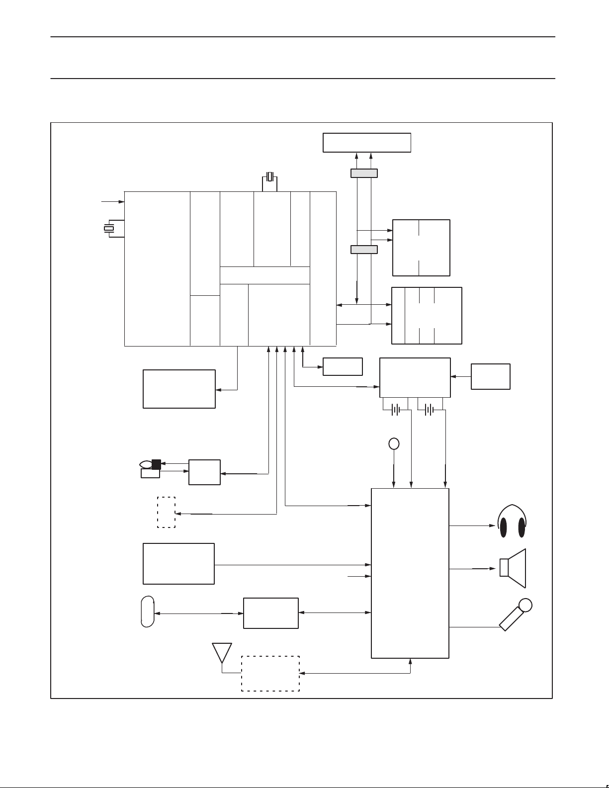
SYSTEM CONFIGURATION
1–2 PCMCIA SLOTS
32KHZ
3.3V
SYSCLK
PR31700
(208–PIN PQFP)
PR3901
RISC
CPU
CORE
LCD
RAM
RAM
IR
I–CACHE/
INTERFACE
I–CACHE/
TLB
32–BIT BUS
LCD
REAL–TIME CLOCK
PCMCIA/ROM/I/F
TIMERS
SERIAL I/F
DRAM/SDRAM INTERFACE
ID ROM
THERMISTOR
MAIN
T
1–64
MBYTES
ROM
1–32
MBYTES(S)
DRAM
POWER
SUPPLY
ADAPTER
BACKUP
(LITHIUM)
AC
1998 May 13
ISDN OR OTHER
PERIPHERALS
PHONE
JACK
TOUCHSCREEN
(RESISTIVE)
HIGH SPEED
SERIAL PORT
DAA
OR
DAA
Figure 1. System Block Diagram
3
3.3V
BETTY
UCB1200
(ANALOG ASIC)
44–PIN QFP
SN00183
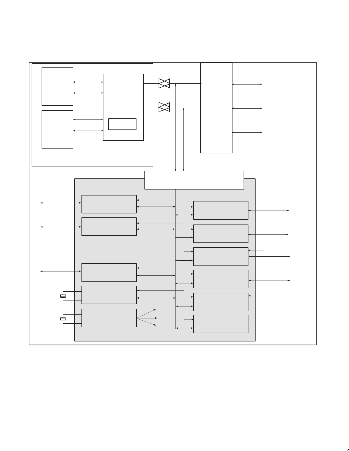
Philips Semiconductors Preliminary specification
PR3170032-bit RISC microprocessor
ICACHE
4 KBYTE
DCACHE
1 KBYTE
TO BETTY
TO LCD
DATA
ADDR
DATA
ADDR
R3901
PROCESSOR CORE
SIB MODULE
VIDEO MODULE
PR3901
RISC CUP
CORE
MAC
DATA
ADDR
SYSTEM INTERFACE UNIT (SIU) MODULE ARBITRATION/
DMA/ADR DECODE
DATA ADDR
BUS INTERFACE UNIT (BIU) MODULE
(S) DRAM/PCMCIA/ROM
CHI MODULE
IR MODULE
DATA
ADDR
CONTROL
TO
MEMORY
TO HIGH
SPEED SERIAL
TO IR
TO GENERAL
PURPOSE I/O
32 KHZ
SYSCLK
IO MODULE
TIMER MODULE
(+ RTC)
CLOCK MODULE
SYSTEM INTERFACE MODULE (SIM)
Figure 2. PR31700 Block Diagram
UART MODULE
(DUAL UART)
SPI MODULE
POWER MODULE
INTERRUPT MODULE
TO UART
TO POWER
SUPPLY
SN00184
1998 May 13
4
Philips Semiconductors Preliminary specification
PR3170032-bit RISC microprocessor
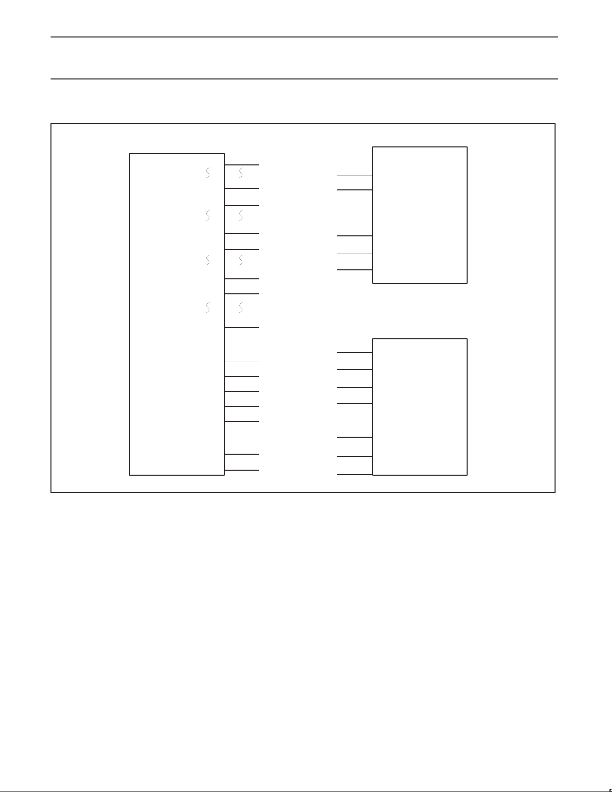
MEMORY CONNECTIONS
PR31700
D[31]
D[24]
D[23]
D[16]
D[15]
D[8]
D[7]
D[0]
CAS3*
CAS2*
CAS1*
CAS0*
RAS0*
WE*
A[12:0]
PIN NO.
133 D[31]
145 D[24]
146 D[23]
159 D[16]
27D[16]
16 D[8]
14 D[7]
2 D[0]
195 CAS3*
197 CAS2*
198 CAS1*
199 CAS0*
194 RAS0*
169 WE*
A[12:0]
CAS1*
CAS0*
RASO*
WE*
A(12:0)
CAS3*
CAS2*
CAS1*
CAS0*
RAS0*
WE*
A(12:0)
CASHI*
CASLO*
RAS*
WE*
ADDR
CAS HI*
CAS MH*
CAS ML*
CAS LO*
RAS*
WE*
ADDR
BANK0
16BIT
DRAM
D(15:0)DATA
BANK1
32BIT
D(31:0)DATA
1998 May 13
BIG ENDIAN
Figure 3. Memory Connections
5
SN00185
Philips Semiconductors Preliminary specification
PR3170032-bit RISC microprocessor
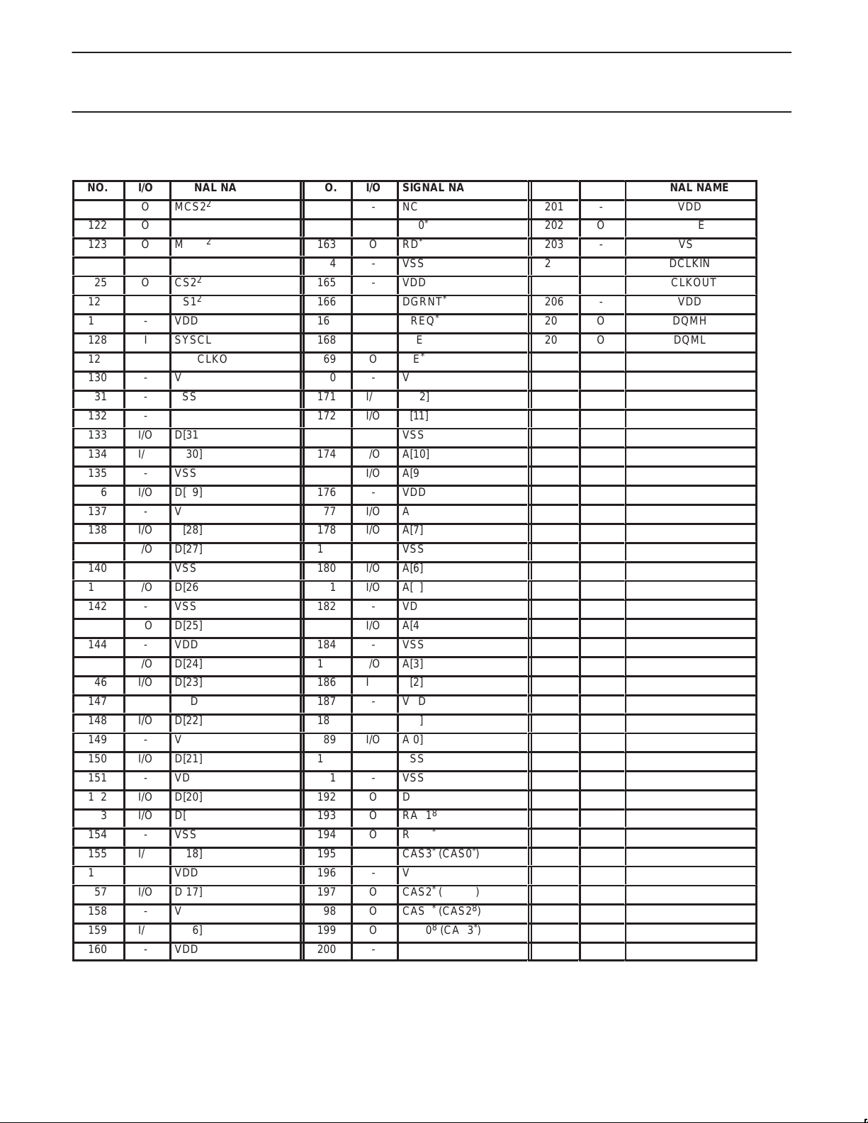
PIN ASSIGNMENTS
NO.
1
2
3
4
5
6
7
8
9
10
11
12
13
14
15
16
17
18
19
20
21
22
23
24
25
26
27
28
29
30
31
32
33
34
35
36
37
38
39
40
I/O
I/O
I/O
I/O
I/O
I/O
I/O
I/O
I/O
I/O
I/O
I/O
I/O
I/O
I/O
I/O
I/O
I/O
I/O
I/O
O
O
O
I
I
SIGNAL NAME
VDD
D[0]
VSS
D[1]
D[2]
VDD
D[3]
VSS
D[4]
VDD
D[5]
D[6]
VSS
D[7]
VSS
D[8]
VDD
D[9]
D[10]
VSS
D[11]
VDD
D[12]
D[13]
VSS
D[14]
D[15]
VDD
ENDIAN
MIOX[1]
RSRV1
NC
VSS
NC
VDD
VDD
SIBMCLK
VSS
SIBSCLK
SIBSYNC
NO.
41
42
43
44
45
46
47
48
49
50
51
52
53
54
55
56
57
58
59
60
61
62
63
64
65
66
67
68
69
70
71
72
73
74
75
76
77
78
79
80
I/O
O
I/O
I/O
I/O
I/O
I/O
O
O
I/O
O
O
I/O
I/O
O
O
O
O
O
I
I
I
I
I
I
I
I
I
I
I
I
SIGNAL NAME
SIBDIN
SIBDOUT
VDD
SIBIRQ
MIOX[0]
IO[6]
IO[5]
VSS
CHICLK
CHIFS
CHIDIN
CHIDOUT
VDD
RXD
TXD
IO[4]
NC
IRIN
IROUT
VSS
VDD
CARDET
RXPWR
IO[3]
IO[2]
VSS
SPICLK
SPIIN
SPIOUT
VDD
TESTCPU
TESTIN
VIDDONE
TESTAIU
VSS
VCC3
BC32K
VDD
C32KlN
C32KOUT
NO.
81
82
83
84
85
86
87
88
89
90
91
92
93
94
95
96
97
98
99
100
101
102
103
104
105
106
107
108
109
110
111
112
113
114
115
116
117
118
119
120
I/O
O
I
I
I
I
I
O
O
O
O
O
O
O
O
O
I/O
I
O
O
I/O
O
O
O
I
O
O
O
O
SIGNAL NAME
VSS
PWRCS
PWRlNT
PWROK
NC
ONBUTN
1
PON
CPURES
*
VDD
DISPON
FRAME
VSS
DF
LOAD
CP
VSS
VDD
VDAT[0]
VDAT[1]
VDAT[2]
VDAT[3]
VSS
IO[1]
VDD
CARD2WAIT
CARD2CSH
CARD2CSL
IO[0]
VSS (PLL)
CARDIORD
CARDIOWR
CARDREG
CARD1WAIT
VDD (PLL)
CARDDIR
*
VDD
CARD1CSL
CARD1CSH
VSS
1
MCS3
8
*
*
*
*
*
*
*
*
1998 May 13
6
Philips Semiconductors Preliminary specification
PR3170032-bit RISC microprocessor
PIN ASSIGNMENTS (Continued)
NO.
121
122
123
124
125
126
127
128
129
130
131
132
133
134
135
136
137
138
139
140
141
142
143
144
145
146
147
148
149
150
151
152
153
154
155
156
157
158
159
160
I/O
O
O
O
O
O
O
I
O
-
-
I/O
I/O
I/O
I/O
I/O
I/O
I/O
I/O
I/O
I/O
I/O
I/O
I/O
I/O
I/O
I/O
-
SIGNAL NAME
2
MCS2
2
MCS1
2
MCS0
2
CS3
2
CS2
2
CS1
VDD
SYSCLKIN
SYSCLKOUT
VSS
VSS
VDD
D[31]
D[30]
VSS
D[29]
VDD
D[28]
D[27]
VSS
D[26]
VSS
D[25]
VDD
D[24]
D[23]
VDD
D[22]
VSS
D[21]
VDD
D[20]
D[19]
VSS
D[18]
VDD
D[17]
VSS
D[16]
VDD
NO.
161
162
163
164
165
166
167
168
169
170
171
172
173
174
175
176
177
178
179
180
181
182
183
184
185
186
187
188
189
190
191
192
193
194
195
196
197
198
199
200
I/O
O
O
-
O
I
O
O
I/O
I/O
I/O
I/O
I/O
I/O
I/O
I/O
I/O
I/O
I/O
I/O
I/O
-
-
O
O
O
O
-
O
O
O
-
SIGNAL NAME
NC
*
CS0
*
RD
VSS
VDD
*
DGRNT
*
DREQ
ALE
*
WE
VDD
A[12]
A[11]
VSS
A[10]
A[9]
VDD
A[8]
A[7]
VSS
A[6]
A[5]
VDD
A[4]
VSS
A[3]
A[2]
VDD
A[1]
A[0]
VSS
VSS
*
DCS0
8
RAS1
*
RAS0
CAS3* (CAS0*)
VDD
CAS2* (CAS1*)
CAS1* (CAS28)
CAS08 (CAS3*)
VSS
NO.
201
202
203
204
205
206
207
208
I/O
SIGNAL NAME
-
O
I
O
O
O
VDD
DCKE
VSS
DCLKIN
DCLKOUT
VDD
DQMH
DQML
1998 May 13
7
Philips Semiconductors Preliminary specification
PR3170032-bit RISC microprocessor
PIN FUNCTIONS
NAME I/O FUNCTIONS
Memory Pins
D(31:0) I/O These pins are the data bus for the system. 8-bit SDRAMs should be connected to bits 7:0 and 16-bit
A(12:0) O These pins are the address bus for the system. The address lines are multiplexed and can be connected
ALE O This pin is used as the address latch enable to latch A(12:0) using an external latch, for generating the
*
RD
O This pin is used as the read signal for static devices. This signal is asserted for reads from /MCS3*-0*,
WE* O This pin is used as the write signal for the system. This signal is asserted for writes to /MCS3*-0*, /CS3*-0*,
CAS0* (/WE0)
CAS* (/WE1)
CAS2* (/WE2)
CAS3* (/WE3)
RAS0
RAS1* (/DCS1)
DCS0
*
*
*
*
*
*
*
O This pin is used as the CAS signal for SDRAMs, the CAS signal for D(7:0) for DRAMs, and the write enable
O This pin is used as the CAS signal for D(15:8) for DRAMs and the write enable signal for D(15:8) for static
O This pin is used as the CAS signal for D(23:16) for DRAMs and the write enable signal for D(23:16) for
O This pin is used as the CAS signal for D(31:24) for DRAMs and the write enable signal for D(31:24) for
O This pin is used as the RAS signal for SDRAMs and the RAS signal for Bank0 DRAMs.
O This pin is used as the chip select signal for Bank1 SDRAMs and the RAS signal for Bank1 DRAMs.
O This pin is used as the chip select signal for Bank0 SDRAMs.
DCKE O This pin is used as the clock enable for SDRAMs.
DCLKIN I This pin must be tied externally to the DCLKOUT signal and is used to match skew for the data input when
DCLKOUT O This pin is the (nominal) 73.728 MHz clock for the SDRAMs.
DQMH O This pin is the upper data mask for a 16-bit SDRAM configuration.
DQML O This pin is the lower data mask for a 16-bit SDRAM or 8-bit SDRAM configuration.
*
CS3–0
MCS3–0
*
CARD2CSH*,L
/CARD1CSH*,L
CARDREG
CARDIORD
CARDIOWR
CARDDIR
CARD2WAIT
CARD1WAIT
*
*
*
*
*
*
*
*
O These pins are the Chip Select 3 through 0 signals. They can be configured to support either 32-bit or 16-bit
O These pins are the Memory Card Chip Select 3 through 0 signals. They only support 16-bit ports.
O These pins are the Chip Select signals for PCMCIA card slot 2.
O These pins are the Chip Select signals for PCMCIA card slot 1.
O This pin is the /REG* signal for the PCMCIA cards.
O This pin is the /IORD* signal for the PCMCIA IO cards.
O This pin is the /IOWR* signal for the PCMCIA IO cards.
O This pin is used to provide the direction control for bi-directional data buffers used for the PCMCIA slot(s).
*Active-low signal
SDRAMs and DRAMs should be connected to bits 15:0. All other 16-bit ports should be connected to bits
31:16. Of course, 32-bit ports should be connected to bits 31:0. These pins are normally outputs and only
become inputs during reads, thus no resistors are required since the bus will only float for a short period of
time during bus turn-around.
directly to SDRAM and DRAM devices. To generate the full 26-bit address for static devices, an external
latch must be used to latch the signals using the ALE signal. For static devices, address bits 25:13 are
provided by the external latch and address bits 12:0 (directly connected from PR31700’s address bus) are
held afterward by PR31700 processor for the remainder of the address bus cycle.
upper address bits 25:13.
/CS3*-0*, /CARD2CS* and /CARD1CS* for memory and attribute space, and for reads from PR31700
processor accesses if SHOWPOSEIDON is enabled (for debugging purposes).
/CARD2CS* and /CARD1CS* for memory and attribute space, and for writes to DRAM and SDRAM.
signal for D(7:0) for static devices.
devices.
static devices.
static devices.
reading from SDRAM and DRAM devices.
ports.
This signal will assert whenever /CARD2CSH* or /CARD2CSL* or /CARD1CSH* or /CARD1CSL* is
asserted and a read transaction is taking place.
I This pin is the card wait signal from PCMCIA card slot 2.
I This pin is the card wait signal from PCMCIA card slot 1.
1998 May 13
8
Philips Semiconductors Preliminary specification
PR3170032-bit RISC microprocessor
NAME
Bus Arbitration Pins
DREQ* I This pin is used to request external arbitration. If the TESTSIU signal is high and the TESTSIU function has
DGRNT* O This pin is asserted in response to /DREQ* to inform the external test logic or bus master that it can now
*Active-low signal
NAME
Clock Pins
SYSCLKIN I This pin should be connected along with SYSCLKOUT to an external crystal which is the main PR31700
SYSCLKOUT O This pin should be connected along with SYSCLKIN to an external crystal which is the main PR31700 clock
C32KIN I This pin along with C32KOUT should be connected to a 32.768 KHz crystal.
C32KOUT O This pin along with C32KIN should be connected to a 32.768 KHz crystal.
BC32K O This pin is a buffered output of the 32.768 KHz clock.
NAME I/O FUNCTIONS
CHI Pins
CHIFS I/O This pin is the CHI frame synchronization signal. This pin is available for use in one of two modes. As an
CHICLK I/O This pin is the CHI clock signal. This pin is available for use in one of two modes. As an output, this pin
CHIDOUT O This pin is the CHI serial data output signal.
CHIDIN I This pin is the CHI serial data input signal.
I/O FUNCTIONS
been enabled, then once /DGRNT* is asserted, external logic can initiate reads or writes to PR31700
processor registers by driving the appropriate input signals. If the TESTSIU signal is low or the TESTSIU
function has not been enabled, then PR31700 memory transactions are halted and certain memory signals
will be tri-stated when /DGRNT* is asserted in order to allow an external master to access memory.
begin to drive signals.
I/O FUNCTIONS
clock source.
source.
output, this pin allows PR31700 to be the master CHI sync source. As an input, this pin allows an external
peripheral to be the master CHI sync source and the PR31700 CHI module will slave to this external sync.
allows PR31700 to be the master CHI clock source. As an input, this pin allows an external peripheral to be
the master CHI clock source and the PR31700 CHI module will slave to this external clock.
NAME I/O FUNCTIONS
IO Pins
IO(6:0) I/O These pins are general purpose input/output ports. Each port can be independently programmed as an
MIO(1:0) I/O These pins are multi-function input/output ports. Each port can be independently programmed as an input
NAME I/O FUNCTIONS
Reset Pins
/CPURES* I This pin is used to reset the CPU core. This pin should be connected to a switch for initiating a reset in the
/PON* I This pin serves as the Power On Reset signal for PR31700. This signal must remain low when VSTANDBY
VSTANDBY—This signal provides power for the PR31700 and other components in the system that must never lose power. This signal should
always be asserted if there is eithr a good Main Backup Battery, or if a Battery Charger is plugged in.
1998 May 13
input or output port. Each port can generate a separate positive and negative edge interrupt. Each port
can also be independently programmed to use a 16 to 24 msec debouncer.
or output port, or can be programmed for multi-function use to support test signals (for debugging purposes
only). Each port can generate a separate positive and negative edge interrupt. Note that 30 other
multi-function pins are available for usage as multi-function input/output ports. These pins are named after
their respective standard/normal function and are not listed here.
event that a software problem might hang the CPU core. The pin should also be pulled up to VSTANDBY*
through an external pull-up resistor.
is asserted until VSTANDBY is stable. Once VSTANDBY is asserted, this signal should never go low
unless all power is lost in the system.
9
Philips Semiconductors Preliminary specification
PR3170032-bit RISC microprocessor
NAME
Power Supply Pins
ONBUTN I This pin is used as the On Button for the system. Asserting this signal will cause PWRCS to set to indicate
PWRCS O This pin is used as the chip select for the System Power Supply. When the system is off, the assertion of
PWROK I This pin provides a status from the System Power Supply that there is a good source of power in the
PWRINT I This pin is used by the System Power Supply to alert the software that some status has changed in the
VCC3 I This pin provides the status of the power supply for the ROM, UCB1200, system buffers, and other transient
VCCDRAM: This signal provides power for the DRAM and/or SDRAM. The supply must be off when VST ANDBY is first asserted, andremain
off until the system is powered up by the assertion of PWRCS. When the software subsequently powers down the system it may choose to keep
this supply on to preserve the contents of memory.
NAME
SIB Pins
SIBDIN I This pin contains the input data shifted from UCB1200 and/or external codec device.
SIBDOUT O This pin contains the output data shifted to UCB1200 and/or external codec device.
SIBSCLK O This pin is the serial clock sent to UCB1200 and/or external codec device. The programmable SIBSCLK
SIBSYNC O This pin is the frame synchronization signal sent to UCB1200 and/or external codec device. This frame
SIBIRQ I This pin is a general purpose input port used for the SIB interrupt source from UCB1200. This interrupt
SIBMCLK I/O This pin is the master clock source for the SIB logic. This pin is available for use in one of two modes. First,
I/O FUNCTIONS
to the System Power Supply to turn power on to the system. PWRCS will not assert if the PWROK signal is
low.
this signal will cause the System Power Supply to turn VCCDRAM and VCC3 on to power up the system.
The Power Supply will latch SPI commands on the falling edge of PWRCS.
system. This signal typically will be asserted if there is a Battery Charger supplying current or if the Main
Battery is good and the Battery Door is closed. If PWROK is low when the system is powered off, PWRCS
will not assert as a result of the user pressing the ONBUTN or an interrupt attempting to wake up the
system. If the device is on when the PWROK signal goes low, the software will immediately shut down the
system since power is about to be lost. When PWROK goes low, there must be ample warning so that the
software can shut down the system before power is actually lost.
System Power Supply and the software should read the status from the System Power Supply to find out
what has changed. These will be low priority events, unlike the PWROK status, which is a high priority
emergency case.
components in the system. This signal will be asserted by the System Power Supply when PWRCS is
asserted, and will always be turned off when the system is powered down.
I/O FUNCTIONS
rate is derived by dividing down from SIBMCLK.
sync is asserted for one clock cycle immediately before each frame starts and all devices connected to the
SIB monitor SIBSYNC to determine when they should transmit or receive data.
source can be configured to generate an interrupt on either a positive and/or negative edge.
SIBMCLK can be configured as a high-rate output master clock source required by certain external codec
devices. In this mode all SIB clocks are synchronously slaved to the main PR31700 system clock CLK2X.
Conversely, SIBMCLK can be configured as an input slave clock source. In this mode, all SIB clocks are
derived from an external SIBMCLK oscillator source, which is asynchronous with respect to CLK2X. Also,
for this mode, SIBMCLK can still be optionally used as a high-rate master clock source required by certain
external codec devices.
NAME I/O FUNCTIONS
SPI Pins
SPICLK O This pin is used to clock data in and out of the SPI slave device.
SPIOUT O This pin contains the data that is shifted into the SPI slave device.
SPIIN I This pin contains the data that is shifted out of the SPI slave device.
NAME I/O FUNCTIONS
UART and IR Pins
TXD O This pin is the UART transmit signal from the UART A module.
RXD I This pin is the UART receive signal to the UART A module.
1998 May 13
10
Philips Semiconductors Preliminary specification
PR3170032-bit RISC microprocessor
NAME FUNCTIONSI/O
IROUT O This pin is the UART transmit signal from the UART B module or the Consumer IR output signal if
IRIN I This pin is the UART receive signal to the UART B module.
RXPWR O This pin is the receiver power output control signal to the external communication IR analog circuitry.
CARDET I This pin is the carrier detect input signal from the external communication IR analog circuitry.
NAME I/O FUNCTIONS
Video Pins
FRAME O This pin is the frame synchronization pulse signal between the Video Module and the LCD, and is used by
DF O This pin is the AC signal for the LCD. Since LCD plasma tends to deteriorate whenever subjected to a DC
LOAD O This pin is the line synchronization pulse signal between the Video Module and the LCD, and is used by the
CP O This pin is the clock signal for the LCD. Data is pushed by the Video Module on the rising edge of CP and
VDAT(3:0) O These pins are the data for the LCD. These signals are directly connected to the LCD for 4-bit non-split
DISPON O This pin is the display-on enable signal for the LCD.
VIDDONE O This pin is used to externally synchronize events to periods whenthe vido is not shifting.
Consumer IR mode is enabled.
the LCD to return it’s pointers to the top of the display . The Video Module asserts FRAME after all the lines
of the LCD have been shifted and transferred, producing a full frame of display.
voltage, the DF signal is used by the LCD to alternate the polarity of the row and column voltages used to
turn the pixels on and off. The DF signal can be configured to toggle on every frame or can be configured to
toggle every programmable number of LOAD signals.
LCD to transfer the contents of it’s horizontal line shift register to the LCD panel for display . The Video
Module asserts LOAD after an entire horizontal line of data has been shifted into the LCD.
sampled by the LCD on the falling edge of CP.
displays. For 4-bit split and 8-bit non-split displays, an external register is required to demultiplex the 4-bit
data into the desired 8 parallel data lines needed for the LCD.
NAME I/O FUNCTIONS
Endian Pin
ENDIAN I This pin is used to select the endianess of the PR31700. The ”1” level input sets the endianess to the big
NAME I/O FUNCTIONS
Test Pins
TESTSIU I This pin allows external logic to initiate read or write transactions to PR31700 registers. The TESTSIU
TESTCPU I This pin allows numerous internal CPU core signals to be brought to external PR31700 pins, in place of the
TESTIN I This pin is reserved for vendor-dependent use. This pin is used for debugging purposes only .
VIDDONE O This signal is used to synchronize UCB1200 to read touchscreen input, when there is no video data shifted
NAME I/O FUNCTIONS
Spare Pins
NC5–1 No
Connect
RSRV1 I These pins are reserved for future use and should be connected to ground.
endian, while the ”0” level input tot he little endian.
mode is enabled by toggling this signal after the device has powered up. Once the function is enabled, if the
TESTSIU pin is high when the bus is arbitrated (using /DREQ and /DGRNT), then external logic can initiate
read and write transactions to PR31700 registers. This pin is used for debugging purposes only.
normal signals assigned to these pins. The CPU core signals assigned to their respective pins during
TESTCPU mode are vendor-dependent. The TESTCPU mode is enabled by asserting this TESTCPU
signal, and this function is provided for generating test vectors for the CPU core. This pin is used for
debugging purposes only.
into LCD panel.
These pins are reserved for future use and should be left unconnected.
1998 May 13
11

Philips Semiconductors Preliminary specification
PR3170032-bit RISC microprocessor
NAME
Power Supply Pins
VDD (33 each) V These pins are the power pins for PR31700 and should be connected to the digital +3.3V power supply
VSS (33 each) G These pins are the ground pins for PR31700 and should be connected to digital ground.
Vdd (for PLL) V This pin is the analog power pin for the PR31700. Keep away from other VDD.
VSS (for PLL) G This pin is the analog ground pin for the PR31700. Keep away from other VSS.
I/O FUNCTIONS
VSTANDBY.
NOTE: For some vendor-dependent implementations of PR31700, pin 131 may be used for a filter
capacitor for the SYSCLK oscillator (capacitor connected between pin 131 and digital ground).
1998 May 13
12

Philips Semiconductors Preliminary specification
Á
Á
Á
Á
Á
Á
Á
Á
Á
Á
Á
Á
Á
Á
Á
PR3170032-bit RISC microprocessor
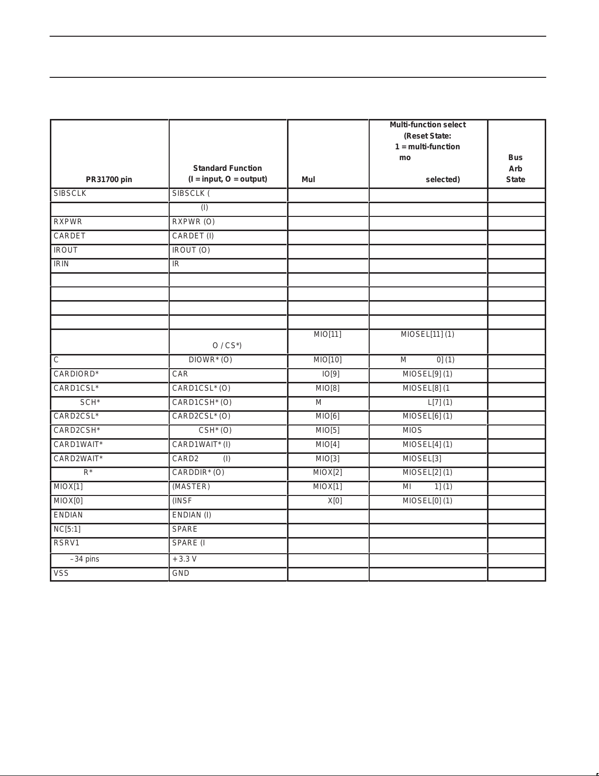
PIN USAGE INFORMATION
This section contains tables summarizing various aspects of the pin
usage for the PR31700. Table 1 lists the standard versus
multi-function usage for each PR31700 pin, if applicable. Those
signal names shown in parentheses are test signals for debugging
purposes only. The column showing the multi-function select signal
Table 1. PR31700 Standard and Multi-Function Pin Usage
БББББББ
БББББББ
БББББББ
PR31700 pin
D[31:0]
A[12:0]
ALE
RD*
WE*
CAS0* (WE0*)
CAS1* (WE1*)
CAS2* (WE2*)
CAS3* (WE3*)
RAS0*
RAS1* (DCS1*)
DCS0*
DCKE
DCLKIN
DCLKOUT
DQMH
DQML
DREQ*
DGRNT*
SYSCLKIN
SYSCLKOUT
C32KlN
C32KOUT
BC32K
VDAT[3]
VDAT[2]
VDAT[1]
VDAT[0]
CP
LOAD
DF
FRAME
БББББББ
БББББББ
Standard Function
БББББББ
(I = input, O = output)
D[31:0] (I/O)
A[12:0] (I/O)
ALE (O)
RD* (O)
WE* (O)
CAS0* (O)
CAS1* (O)
CAS2* (O)
CAS3* (O)
RAS0* (O)
RAS1* (O)
DCS0* (O)
DCKE (O)
DCLKIN (I)
DCLKOUT (O)
DQMH (O)
DQML (O)
DREQ* (I)
DGRNT* (O)
SYSCLKIN (I)
SYSCLKOUT (O)
C32KIN (I)
C32KOUT (O)
BC32K(O)
VDAT[3] (O)
VDAT[2] (O)
VDAT[1] (O)
VDAT[0] (O)
CP (O)
LOAD (O)
DF (O)
FRAME (O)
ÁÁÁÁ
ÁÁÁÁ
ÁÁÁÁ
Multi-function
and reset state indicates the internal control signal used to select the
multi-function mode, as well as the default configuration of each
multi-function pin during reset. The ”Bus Arb State” column shows
which pins are tri-stated whenever the DGRNT* signal is asserted in
response to a DREQ*(external bus arbitration request).
Multi-function select
(Reset State:
БББББББ
1 = multi-function
mode selected;
БББББББ
0 = standard function
БББББББ
& mode selected)
ÁÁÁ
Bus
ÁÁÁ
Arb
ÁÁÁ
State
Hi-Z
Hi-Z
Hi-Z
Hi-Z
Hi-Z
Hi-Z
Hi-Z
Hi-Z
Hi-Z
Hi-Z
Hi-Z
Hi-Z
Hi-Z
Hi-Z
Hi-Z
MIO[27]
MIO[26]
MIO[25]
(BERR)
(IRQHIGH)
(IRQLow)
MIOSEL[27] (0)
MIOSEL[26] (0)
MIOSEL[25] (1)
IRQTEST (0)
IRQTEST (0)
IRQTEST (0)
1998 May 13
13

Philips Semiconductors Preliminary specification
Á
Á
Á
Á
Á
Á
Á
Á
Á
Á
Á
Á
Á
Á
Á
Á
Á
Á
Á
Á
PR3170032-bit RISC microprocessor
Table 1. PR31700 Standard and Multi-Function Pin Usage (Continued)
БББББББ
БББББББ
БББББББ
БББББББ
PR31700 pin
DISPON
PWRCS
PWRINT
PWROK
ONBUTN
CPURES*
PON*
TXD
RXD
CS0*
CS1*
CS2*
CS3*
MCS0*
MCS1*
MCS2*
MCS3*
CHIFS
CHICLK
CHIDOUT
CHIDIN
VCC3
IO6
IO5
IO4
IO3
IO2
IO1
IO0
SPICLK
SPIOUT
SPIIN
SIBSYNC
SIBDOUT
SIBDIN
SIBMCLK
БББББББ
БББББББ
БББББББ
Standard Function
БББББББ
(I = input, O = output)
DISPON (O)
PWRCS (O)
PWRINT (I)
PWROK (I)
ONBUTN (I)
CPURES* (I)
PON* (I)
TXD (O)
RXD (I)
CS0* (O)
CS1* (O)
CS2* (O)
CS3* (O)
MCS0* (O)
MCS1* (O)
MCS2* (O)
MCS3* (O)
CHIFS (I/O)
CHICLK (I/O)
CHIDOUT (O)
CHIDIN (I)
VCC3 (I)
IO6 (I/O)
IO5 (I/O)
IO4 (I/O)
IO3 (I/O)
IO2 (I/O)
IO1 (I/O)
IO0 (I/O)
SPICLK (O)
SPIOUT (O)
SPIIN (I)
SIBSYNC (O)
SIBDOUT (O)
SIBDIN (I)
SIBMCLK (I/O)
ÁÁÁÁ
ÁÁÁÁ
ÁÁÁÁ
ÁÁÁÁ
Multi-function
MIO[24]
MIO[23]
MIO[22]
MIO[21]
MIO[20]
MIO[19]
MIO[18]
MIO[17]
MIO[16]
MIO[31]
MIO[30]
MIO[29]
MIO[28]
MIO[15]
MIO[14]
MIO[13]
MIO[12]
Multi-function select
БББББББ
(Reset State:
1 = multi-function
БББББББ
mode selected;
БББББББ
0 = standard function
БББББББ
& mode selected)
MIOSEL[24] (0)
MIOSEL[23] (0)
MIOSEL[22] (0)
MIOSEL[21] (0)
MIOSEL[20] (0)
MIOSEL[19] (1)
MIOSEL[18] (1)
MIOSEL[17] (1)
MIOSEL[16] (1)
MIOSEL[31] (1)
MIOSEL[30] (1)
MIOSEL[29] (1)
MIOSEL[28] (1)
MIOSEL[15] (0)
MIOSEL[14] (0)
MIOSEL[13] (0)
MIOSEL[12] (0)
ÁÁÁ
ÁÁÁ
Bus
ÁÁÁ
Arb
ÁÁÁ
State
Hi-Z
1998 May 13
14
Philips Semiconductors Preliminary specification
Á
Á
Á
Á
Á
Á
Á
Á
Á
Á
Á
Á
Á
Á
Á
Á
Á
Á
Á
Á
Á
Á
Á
Á
Á
PR3170032-bit RISC microprocessor
Table 1. PR31700 Standard and Multi-Function Pin Usage (Continued)
БББББББ
БББББББ
БББББББ
БББББББ
PR31700 pin
SIBSCLK
SIBIRQ
RXPWR
CARDET
IROUT
IRIN
TESTAIU
TESTCPU
TESTIN
VIDDONE
CARDREG*
БББББББ
CARDIOWR*
CARDIORD*
CARD1CSL*
CARD1SCH*
CARD2CSL*
CARD2CSH*
CARD1WAIT*
CARD2WAIT*
CARDDIR*
MIOX[1]
MIOX[0]
ENDIAN
NC[5:1]
RSRV1
VDD–34 pins
VSS–34 pins
БББББББ
БББББББ
БББББББ
Standard Function
БББББББ
(I = input, O = output)
SIBSCLK (O)
SIBIRQ (I)
RXPWR (O)
CARDET (I)
IROUT (O)
IRIN (I)
TESTAIU (I)
TESTCPU (I)
TESTIN (I)
VIDDONE (O)
CARDREG*(O)
БББББББ
(SHOWDINO / CS*)
CARDIOWR* (O)
CARDIORD* (O)
CARD1CSL* (O)
CARD1CSH* (O)
CARD2CSL* (O)
CARD2CSH* (O)
CARD1WAIT* (I)
CARD2WAIT* (I)
CARDDIR* (O)
(MASTER)
(INSFETCH*)
ENDIAN (I)
SPARE
SPARE (I)
+ 3.3 V
GND
ÁÁÁÁ
ÁÁÁÁ
ÁÁÁÁ
ÁÁÁÁ
Multi-function
MIO[11]
ÁÁÁÁ
MIO[10]
MIO[9]
MIO[8]
MIO[7]
MIO[6]
MIO[5]
MIO[4]
MIO[3]
MIOX[2]
MIOX[1]
MIOX[0]
Multi-function select
БББББББ
(Reset State:
1 = multi-function
БББББББ
mode selected;
БББББББ
0 = standard function
БББББББ
& mode selected)
MIOSEL[1 1] (1)
БББББББ
MIOSEL[10] (1)
MIOSEL[9] (1)
MIOSEL[8] (1)
MIOSEL[7] (1)
MIOSEL[6] (1)
MIOSEL[5] (1)
MIOSEL[4] (1)
MIOSEL[3] (1)
MIOSEL[2] (1)
MIOSEL[1] (1)
MIOSEL[0] (1)
ÁÁÁ
ÁÁÁ
Bus
ÁÁÁ
Arb
ÁÁÁ
State
ÁÁÁ
1998 May 13
15

Philips Semiconductors Preliminary specification
PR3170032-bit RISC microprocessor
Table 2 lists various power-down states and conditions for each PR31700 pin. The ”Power-Down Control” column shows the conditions which
trigger a power-down for each respective pin. This column also shows the reset state for each of these conditions.
The ”PON* state” column defines the state of each pin at power-on reset (PON*). This condition is defined as initial power up of the
PR31700, whereby the PR31700 is initialized and the PR31700 pins are reset to the state shown in the table. This state is entered
after power is applied for the very first time (VSTANDBY is turned on but VCC3 is still turned off).
The ”1st-time power-up state” column defines the state of each pin after power-up mode (RUNNING STATE) is executed for the
first time. This mode is defined as VCC3 applied to the entire system and is initiated by the user pressing the ONBUTN while in
the power-on reset (PON*) state. Note that the defined state of various pins for 1st-time power-up may depend on the configuration
of external devices attached to these pins. After 1st-time power-up, the software could change the state of various pins to be
different from those shown in the table. Thereafter , subsequent transitions from SLEEP STATE to RUNNING STATE might result in
different states for these pins.
The ”power-down state” column defines the state of each pin during power-down mode (SLEEP STATE). This mode is defined as
VCC3 turned off to the entire system, except for the PR31700 (RTC and interrupts alive) and any persistent memory.
1998 May 13
16

Philips Semiconductors Preliminary specification
Á
Á
Á
Á
Á
Á
Á
Á
Á
Á
PR3170032-bit RISC microprocessor
Table 2. PR31700 Power-Down Pin Usage
ББББББ
PR31700 pin
ББББББ
D[31:0]
A[12:0]
ALE
RD*
WE*
CAS0* (WE0*)
CAS1* (WE1*)
CAS2* (WE2*)
CAS3* (WE3*)
RAS0*
RAS1* (DCS1*)
DCS0*
DCKE
DCLKIN
DCLKOUT
DQMH
DQML
DREQ*
DGRNT*
SYSCLKIN
SYSCLKOUT
C32KIN
C32KOUT
BC32K
VDAT[3]
VDAT[2]
VDAT[1]
VDAT[0]
CP
LOAD
DF
FRAME
DISPON
PWRCS
PWRINT
PWROK
ONBUTN
CPURES*
PON*
MBUSCLK
ББББББББББ
ББББББББББ
Power-Down Control
powerdown = (vccon & vcc3)*
(reset state)
MEMPOWERDOWN
MEMPOWERDOWN
POWERDOWN
MEMPOWERDOWN
MEMPOWERDOWN
MEMPOWERDOWN
MEMPOWERDOWN
MEMPOWERDOWN
MEMPOWERDOWN
MEMPOWERDOWN
MEMPOWERDOWN
MEMPOWERDOWN
MEMPOWERDOWN
MEMPOWERDOWN
MEMPOWERDOWN
POWERDOWN & MIOPD[27] (1)
POWERDOWN & MIOPD[26] (0)
POWERDOWN
POWERDOWN
POWERDOWN & MIOPD[25] (1)
MODULE DISABLE
MODULE DISABLE
MODULE DISABLE
MODULE DISABLE
MODULE DISABLE
MODULE DISABLE
MODULE DISABLE
MODULE DISABLE
MODULE DISABLE
MODULE DISABLE
ÁÁÁÁ
PON* state
ÁÁÁÁ
Low
Low
Low
Low
Low
Low
Low
Low
Low
Low
Low
Low
Low
Low
Low
Low
Pull-Down
Low
OSC off
OSC off
OSC on
OSC on
Pull-Down
Low
Low
Low
Low
Low
Low
Low
Low
Low
Low
Out Low
1st time
ÁÁÁÁ
power-up
state
ÁÁÁÁ
Low
Low
Low
Hi
Low
Low
Low
Low
Low
Low
Low
Low
Low
Low
Low
Low
In
Hi
OSC on
OSC on
OSC on
OSC on
In
Low
Low
Low
Low
Low
Low
Low
Low
Low
Hi
Out Low
ÁÁÁÁ
power-down
state
ÁÁÁÁ
Low
Low
Low
Low
Low
Low
Low
Low
Low
Low
Low
Low
Low
Low
Low
Low
Selectable
Selectable
OSC off
OSC off
OSC on
OSC on
Selectable
Low
Low
Low
Low
Low
Low
Low
Low
Low
Low
Out Low
1998 May 13
17

Philips Semiconductors Preliminary specification
Á
Á
Á
Á
Á
Á
Á
Á
Á
Á
PR3170032-bit RISC microprocessor
Table 2. PR31700 Power-Down Pin Usage (Continued)
ББББББ
PR31700 pin
ББББББ
MBUSDATA
MBUSINT
TXD
RXD
CS0*
CS1*
CS2*
CS3*
MCS0*
MCS1*
MCS2*
MCS3*
CHIFS
CHICLK
CHIDOUT
CHIDIN
VCC3
IO6
IO5
IO4
IO3
IO2
IO1
IO0
SPICLK
SPIOUT
SPIIN
SIBSYNC
SIBDOUT
SIBDIN
SIBMCLK
SIBSCLK
SIBIRQ
RXPWR
CARDET
IROUT
IRIN
TESTAIU
TESTCPU
TESTIN
VIDDONE
ББББББББББ
ББББББББББ
Power-Down Control
powerdown = (vccon & vcc3)*
(reset state)
MODULE DISABLE
POWERDOWN & MIOPD[24] (0)
POWERDOWN & MIOPD[23] (1)
POWERDOWN
POWERDOWN & MIOPD[22] (1)
POWERDOWN & MIOPD[21] (1)
POWERDOWN & MIOPD[20] (1)
POWERDOWN & MIOPD[19] (0)
POWERDOWN & MIOPD[18] (0)
POWERDOWN & MIOPD[17] (0)
POWERDOWN & MIOPD[16] (0)
POWERDOWN & MIOPD[31] (1)
POWERDOWN & MIOPD[30] (1)
POWERDOWN & MIOPD[29] (1)
POWERDOWN & MIOPD[28] (1)
POWERDOWN
POWERDOWN & IOPD[6] (1)
POWERDOWN & IOPD[5] (1)
POWERDOWN & IOPD[4] (1)
POWERDOWN & IOPD[3] (1)
POWERDOWN & IOPD[2] (1)
POWERDOWN & IOPD[1] (1)
POWERDOWN & IOPD[0] (1)
POWERDOWN & MIOPD[15] (0)
POWERDOWN & MIOPD[14] (0)
POWERDOWN & MIOPD[13] (1)
POWERDOWN
POWERDOWN
POWERDOWN
POWERDOWN & MIOPD[12] (1)
POWERDOWN
POWERDOWN
POWERDOWN
POWERDOWN
POWERDOWN
POWERDOWN
MODULE DISABLE
ÁÁÁÁ
PON* state
ÁÁÁÁ
Out Low
Low
Pull-Down
Pull-Down
Pull-Down
Pull-Down
Pull-Down
In
In
In
In
Pull-Down
Pull-Down
Pull-Down
Pull-Down
Pull-Down
Pull-Down
Pull-Down
Pull-Down
Pull-Down
Pull-Down
Pull-Down
Pull-Down
Low
Low
Pull-Down
Low
Low
Pull-Down
Pull-Down
Low
Pull-Down
Low
Pull-Down
Low
Pull-Down
Low
1st time
ÁÁÁÁ
power-up
state
ÁÁÁÁ
Out Low
Low
In
Hi
Hi
Hi
Hi
IN
IN
IN
IN
IN
IN
IN
IN
IN
IN
IN
IN
IN
IN
IN
Low
Low
Low
Low
IN
Low
Low
Low
Low
ÁÁÁÁ
power-down
state
ÁÁÁÁ
Out Low
Selectable
Selectable
Pull-Down
Selectable
Selectable
Selectable
Selectable
Selectable
Selectable
Selectable
Selectable
Selectable
Selectable
Selectable
Pull-Down
Selectable
Selectable
Selectable
Selectable
Selectable
Selectable
Selectable
Selectable
Selectable
Selectable
Low
Low
Pull-Down
Selectable
Low
Pull-Down
Low
Pull-Down
Low
Pull-Down
Low
1998 May 13
18

Philips Semiconductors Preliminary specification
Á
Á
Á
Á
Á
Á
Á
Á
Á
Á
PR3170032-bit RISC microprocessor
Table 2. PR31700 Power-Down Pin Usage (Continued)
ББББББ
PR31700 pin
ББББББ
CARDREG*
CARDIOWR*
CARDIORD*
CARD1CSL*
CARD1CSH*
CARD2CSL*
CARD2CSH*
CARD1WAIT*
CARD2WAIT*
CARDDIR*
MIOX[1]
MIOX[0]
ENDIAN
NC[5:1]
RSRV1
VDD–34 EACH
VSS–34 EACH
ББББББББББ
ББББББББББ
Power-Down Control
powerdown = (vccon & vcc3)*
(reset state)
POWERDOWN & MIOPD[11] (1)
POWERDOWN & MIOPD[10] (1)
POWERDOWN & MIOPD[9] (1)
POWERDOWN & MIOPD[8] (1)
POWERDOWN & MIOPD[7] (1)
POWERDOWN & MIOPD[6] (1)
POWERDOWN & MIOPD[5] (1)
POWERDOWN & MIOPD[4] (1)
POWERDOWN & MIOPD[3] (1)
POWERDOWN & MIOPD[2] (1)
POWERDOWN & MIOPD[1] (0)
POWERDOWN & MIOPD[0] (0)
ÁÁÁÁ
PON* state
ÁÁÁÁ
Pull-Down
Pull-Down
Pull-Down
Pull-Down
Pull-Down
Pull-Down
Pull-Down
Pull-Down
Pull-Down
Pull-Down
IN
IN
1st time
ÁÁÁÁ
power-up
state
ÁÁÁÁ
IN
IN
IN
IN
IN
IN
IN
IN
IN
IN
IN
IN
ÁÁÁÁ
power-down
state
ÁÁÁÁ
Selectable
Selectable
Selectable
Selectable
Selectable
Selectable
Selectable
Selectable
Selectable
Selectable
Selectable
Selectable
1998 May 13
19

Philips Semiconductors Preliminary specification
PR3170032-bit RISC microprocessor
FUNCTION SPECIFICA TIONS
OUTLINE
The PR31700 consists of system support logic, integrated with the
PR3901 Processor Core designed by Philips. For details of the
system support logic and the PR3901 Processor Core, refer to the
PR31700 User’s Manual.
PR3901 PROCESSOR CORE
The PR3901 is a Philips-developed microprocessor core based on
the R3000A RISC architecture developed by MIPS Technologies,
Inc.
INSTRUCTIONS
All PR3901 Processor Core instructions are 32-bit instructions.
Apart from some coprocessor instructions, the instructions are
upwardly compatible with the R3000A. The PR3901 Processor Core
instructions can be classified into six types.
• Load and store instructions
– Transfer data between memory and general-purpose registers.
• Computational instructions
– These include arithmetic, logical, shift, multiply, divide, and
multiply-add instructions. The multiply-add instructions are
extensions to the R3000A. The multiply instructions can also
be used as three-operand instructions.
• Special instructions
– Used for system call or break point.
• Jump and branch instructions
– Change the control flow of a program. The Branch-Likely
instruction is provided as an extension to the R3000A.
• Coprocessor instructions
– Perform operations for coprocessors. The R3000A LWCz and
SWCz instructions are reserved instructions in the PR3901
Processor Core. Attempting execution generates a reserved
instruction exception. Note that the COPz, CTCz and MTCz
instructions are no-operation instructions, the CFCz and MFCz
instructions load undefined data to general purpose registers
(rt) in the PR31700.
• System control coprocessor instructions
– Perform operations on the CP0 registers to manipulate the
memory management and exception handling functions of the
processor.
REGISTERS
The PR3901 Processor Core has following registers.
• 32 general purpose registers (32-bit)
• HI/LO registers
– Hold the result of multiply and divide operation
• PC (Program Counter)
• Cause register
– Indicates the nature of the most recent exception
• EPC (Exception Program Counter) register
– Holds the program counter at the time the exception occurred,
indicating the address where processing is to resume after the
exception processing is completed.
• Status register
– Holds the operating mode status (user mode or kernel mode),
interrupt masking status, diagnosis status and other such
information.
• BadVAddr (Bad Virtual Address) register
– Holds the most recent virtual address for which a virtual
address translation error occurred.
• PRId register
– Shows the revision number of the PR3901 Processor Core.
– Cache register
– Controls the instruction cache (reserved) and the data cache
auto-lock bits.
• Debug register
– Control software debug exception.
• DEPC
– Program counter for software debug exception.
MEMORY MANAGEMENT
The PR3901 Processor Core has a 4G-byte memory address
space. The 4G-byte memory space consists of a 2G-byte user area
and a 2G-byte kernel area. The kernel area contains a cache area
and an uncache area.The PR3901 Processor Core provides a
full-featured memory management unit (MMU) utilizing an on-chip
Translation Lookaside Buffer (TLB). The on-chip TLB majur
characteristics are :
• 32 x 64-bit wide entries
• fully associative
• 2 entry micro TLB for instruction address translation
• instruction address translation accesses full TL after micro-TLB
miss
• data address translation accesses full TLB
PIPELINE
The PR3901 Processor Core pipeline consists of five stages. The
pipeline configuration enables the PR3901 Processor Core to
execute nearly all instructions in one clock.
CACHE
The PR31700 incorporates a 4K-byte instruction cache and a
1K-byte data cache. The instruction cache is direct-mapped with a
block size of 16 bytes. The data cache uses two-way set-associative
mapping with a block size of four bytes. The data cache has a lock
function that locks data in one direction. The write-through method
is used to write data back to memory.
DSP FUNCTION
The PR3901 Processor Core has a high-speed
multiplier/accumulator and supports 32-bit multiplier operations, with
64-bit accumulator in one cycle.
1998 May 13
20

Philips Semiconductors Preliminary specification
PR3170032-bit RISC microprocessor
PERIPHERAL FUNCTIONS
CLOCK GENERATOR
The PR31700 uses an internal PLL and an external crystal oscillator
to generate a clock with eight times the input clock frequency. The
PLL oscillation can be halted externally to reduce power dissipation.
WRITE BUFFER
The PR31700 incorporates a four-stage write buffer.
BUS INTERFACE UNIT (BIU) MODULE
The PR31700 has a Bus Interface Unit with the following features.
• supports 2 Banks of SDRAM and/or DRAM / HDRAM
– 8-bit or 16-bit SDRAM configuration
– 16-bit or 32-bit DRAM configuration
– 16-bit or 32-bit HDRAM configuration
– 4 Mbit, 16 Mbit and 64 Mbit parts supported
– page mode reads and writes supported
– independent refresh counters for each bank
– self refreshing parts supported to retain memory when
system is powered down
• 4 general purpose chip selects (CS3*–CS0*)
– 16-bit or 32-bit ports
– programmable wait states
– read page mode
• 4 general purpose chip selects (MCS3*–MCS0*)
– 16-bit ports
– programmable wait states
– read page mode
• 2 full PCMCIA slots
– 16-bit ports
– IORD and IOWR provided to support I/O cards
– WAIT signal supported
SYSTEM INTERFACE UNIT (SIU) MODULE
The PR31700 has a System Interface Unit with the following
features.
• multi-channel 32-bit DMA controller
• independent DMA controller for video, SIB to/from BETTY
audio/telecom codecs, high-speed serial port, IR, UART, and
general purpose UART
• address decoding for the internal registers
CLOCK MODULE
The PR31700 has a Clock Module with the following features.
• The PR31700 supports system-wide single crystal
configuration, besides the 32 kHz RTC XTAL (reduces cost,
power, and board space)
• common crystal rate divided to generate clock for CPU,
video, sound, telecom, UARTs, etc.
• independent enabling or disabling of individual clocks under
software control, for power management
CONCENTRATION HIGHWAY INTERFACE (CHI) MODULE
The PR31700 has a CHI Module with the following features.
• high-speed serial Concentration Highway Interface (CHI)
contains logic for interfacing to external full-duplex serial
time-division-multiplexed (TDM) communication peripherals
• supports ISDN line interface chips and other PCM/TDM
serial devices
• CHI interface is programmable (number of channels, frame
rate, bit rate, etc.) to provide support for a variety of
formats
• supports data rates up to 4.096 Mbps
• independent DMA support for CHI receive and transmit
INTERRUPT MODULE
The PR31700 has an Interrupt Module with the following features.
• contains logic for individually enabling, reading, and clearing
all PR31700 interrupt sources
• interrupts generated from internal PR31700 modules or from
edge transitions on external signal pins
IO MODULE
The PR31700 has an IO Module with the following features.
• contains support for reading and writing the 7 bi-directional
general purpose IO pins and the 32 bi-directional
multi-function IO pins
• each IO port can generate a separate positive and negative
edge interrupt
• independently configurable IO ports allow the PR31700 to
support a flexible and wide range of system applications and
configurations
IR MODULE
The PR31700 has an IR Module with the following features.
• IR consumer mode
– allows control of consumer electronic devices such as
stereos, TVs, VCRs, etc.
– programmable pulse parameters
– external analog LED circuitry
• IRDA communication mode
– not compatible with General Magic Cap Devices
– allows communication with other IRDA devices such as
FAX machines, copiers, printers, etc.
– supported by the UART module within the PR31700
– external analog receiver preamp and LED circuitry
– data rate = up to 115 kbps at 1 meter
• IR FSK communication mode
– compatible with GeneraI Magic Cap Devices
– supported by the UART module within the PR31700
– external analog IR chip(s) perform frequency modulation to
generate the desired IR communication mode protocol
– data rate = up to 36000 bps at 3 meters
• carrier detect state machine
– periodically enables IR receiver to check if a valid carrier
is present
1998 May 13
21

Philips Semiconductors Preliminary specification
PR3170032-bit RISC microprocessor
POWER MODULE
The PR31700 has a Power Module with the following features.
• power-down modes for individual internal peripheral modules
• serial (SPI port) power supply control interface supported
• power management state machine has 3 states: RUNNING,
DOZING and SLEEP
SERIAL INTERCONNECT BUS (SIB) MODULE
The PR31700 has a SIB Module with the following features.
• The PR31700 contains holding and shift registers to support
the serial interface to the UCB1200 ASIC and/or other
optional codec devices
• synchronous, frame-based protocol
• The PR31700 always master source of clock and frame
frequency and phase; programmable clock frequency
• each SIB frame consists of 128 clock cycles, further divided
into 2 subframes or words of 64 bits each (supports up to 2
devices simultaneously)
• independent DMA support for audio receive and transmit,
telecom receive and transmit
• supports 8-bit or 16-bit mono telecom formats
• supports 8-bit or 16-bit mono or stereo audio formats
• independently programmable audio and telecom sample rates
• CPU read/write registers for subframe control and status
SERIAL PERIPHERAL INTERFACE (SPI) MODULE
The PR31700 has an SPI Module with the following features.
• provides interface to SPI peripherals and devices
• full-duplex, synchronous serial data transfers (data in, data
out, and clock signals)
• The PR31700 supplies dedicated chip select and interrupt for
an SPI interface serial power supply
• 8-bit or 16-bit data word lengths for the SPI interface
• programmable SPI baud rate
TIMER MODULE
The PR31700 has a Timer Module with the following features.
• Real Time Clock (RTC) and Timer
• 40-bit counter (30.517 s granularity);
maximum uninterrupted time = 388.36 days
• 40-bit alarm register (30.517 s granularity)
• 16-bit periodic timer (0.868 s granularity);
maximum timeout = 56.8 ms
• interrupts on alarm, timer, and prior to RTC roll-over
UART MODULE
The PR31700 has a UART Module with the following features.
• 2 independent full-duplex UARTs
• programmable baud rate generator
• UART A port used for serial control interface to external IR
module
• UART B port used for general purpose serial control interface
• UART A and UART B DMA support for receive and transmit
VIDEO MODULE
The PR31700 has a Video Module with the following features.
• bit-mapped graphics
• supports monochrome, grey scale, or color modes
• time-based dithering algorithm for gray scale and color
modes
• supports multiple screen sizes
• supports split and non-split displays
• variable size and relocatable video buffer
• DMA support for fetching image data from video buffer
1998 May 13
22

Philips Semiconductors Preliminary specification
SYMBOL
PARAMETER
UNIT
PR3170032-bit RISC microprocessor
ELECTRICAL CHARACTERISTICS
ABSOLUTE MAXIMUM RA TINGS
VSS = 0 V (GND)
SYMBOL
V
DD
V
IN
T
stg
Pd Maximum dissipation (T
NOTE:
1. Using an LSI at specifications higher than the maximum ratings can cause permanent damage to the LSI. For normal operation, use under
the recommended operating conditions. Exceeding the recommended operating conditions may affect the reliability of the LSI.
Power supply voltage VSS – 0.5 to 4.5 V
Input voltage VSS – 0.5 to VDD + 0.5 V
Storage temperature range –55 to +125 °C
RECOMMENDED OPERATING CONDITIONS
VSS = 0 V (GND)
V
DD
T
opr
Power supply voltage 3.0 3.3 3.6 V
Operating temperature range 0 – 70 °C
PARAMETER LIMITS UNIT
= 70°C) 1 W
amb
LIMITS
MIN TYP MAX
1998 May 13
23

Philips Semiconductors Preliminary specification
SYMBOL
PARAMETER
CONDITIONS
UNIT
PR3170032-bit RISC microprocessor
DC CHARACTERISTICS
(T
= 0°C to 70°C, VDD = 3.3V0.3V)
amb
LIMITS
MIN TYP MAX
I
I
DDS,
I
DDS,
V
V
V
V
V
V
V
V
V
V
V
V
I
DD
I
IN
IH1
IL1
IH2
IL2
OH1
OL1
OH2
OL2
OH3
OL3
OH4
OL4
IHP
Operating current
P Static current
Q
Input leakage current VIN = VDD or V
Input voltage
Input voltage
Input voltage
Input voltage
Output voltage
Output voltage
Output voltage
Output voltage
Output voltage
Output voltage
Output voltage
Output voltage
1
1
2
2
3
3
4
4
5
5
6
6
Input current (Pull–down resister) VDD = MAX; VIN = V
NOTES:
1. SYSVLKIN
2. Other inputs
3. D[31:0], RAS0*, RAS1*, DCS0*, DCKE*, DQMH, DQML, DREQ*, DGRNT*, BC32K, VDAT[3:0], CP, LOAD, DF, FRAME, DISPON,
VIDDONE, PWRCS, TXD, RXD, CS3∼O*,CHIFS, CHICLK, CHIDOUT, CHIDIN, IO[6;0], SPICLK, SPIOUT, SPIIN, SIBSYNC, SIBDOUT,
SIBMCLK, SIBCLK, RWPWR, IROUT, CARD1WAIT*, CARD2WAIT*, MIOX[2;0]
4. A[12:], ALE, RD*, WE* CAS3∼O*, CARDREG*, CARDIOWR*, CARD1CSL*, CARD1CSH*, CARD2CSL*, CARD2CSH*
5. DCLKOUT
6. MBUSCLK, MBUSDATA
VIN = VDD or VSS; VDD = MAX
IOH = IOL = 0
– 110 130 mA
VIN = VDD or VSS; VDD = MAX
I
= IOL = 0 mA
OH
SLEEP mode & RTC stop mode
– 10 100 µA
VIN = VDD or VSS; VDD = MAX
IOH = IOL = 0 mA
SLEEP mode & RTC running
– 20 120 µA
mode
SS
–10 – 10 µA
VDD = 3.6V VDD × 0.8 – VDD + 0.3 V
VDD = 3.0V –0.3 – VDD × 0.2 V
VDD = 3.6V 2.4 – VDD + 0.3 V
VDD = 3.0V –0.3 – 0.6 V
VDD = 3.0V; IOH = –4mA VDD – 0.6 – – V
VDD = 3.0V; IOL = 4mA – – VDD + 0.4 V
VDD = 3.0; IOH = –8mA VDD – 0.6 – – V
VDD = 3.0; IOL = 8mA – – VDD + 0.4 V
VDD = 3.0; IOH = –16mA VDD – 0.6 – – V
VDD = 3.0; IOL = 16mA – – VDD + 0.4 V
VDD = 3.0; IOH = –24mA VDD – 0.6 – – V
VDD = 3.0; IOL = 24mA – – VDD + 0.4 V
DD
20 – 120 µA
1998 May 13
24

Philips Semiconductors Preliminary specification
SYMBOL
PARAMETER
UNIT
fINCrystal Oscillator frequency
8.25
10
MHz
SYMBOL
PARAMETER
UNIT
PR3170032-bit RISC microprocessor
CRYSTAL OSCILLATOR CHARACTERISTICS
PR31700
SYSCKIN
C
IN
X1TAL
Figure 4. 10MHz Crystal
SYSCLKOUT
RECOMMENDED 9.216MHz CRYSTAL
NIHON DEMPA KOGYO CO., LTD: AT–51
C
OUT
SN00191
RECOMMENDED VALUE
MIN. MAX.
CIN, C
CIN, C
OUT
OUT
External capacitors 10 33 pF
PR31700
C32KIN C32KOUT
RECOMMENDED 32.768kHz CRYSTAL
C
IN
X1TAL
KYOCERA CORPORATION: KF–38G
C
OUT
SN00192
Figure 5. 32 kHz Crystal
RECOMMENDED VALUE
MIN. MAX.
External capacitors 10 33 pF
1998 May 13
25

Philips Semiconductors Preliminary specification
БББББББББ
Á
Á
Á
Á
БББББББББ
Á
Á
Á
Á
Á
Á
Á
Á
Á
Á
Á
Á
Á
БББББББББ
Á
Á
Á
Á
Á
Á
PR3170032-bit RISC microprocessor
ELECTRICAL SPECIFICATIONS
= 0V, VDD = 3.3V)
(V
SS
Parameter
Crystal stabilization time
БББББББ
9.216MHz
БББББББ
Crystal stabilization time
32.768kHz
БББББББ
PR31700 TIMING
OUTPUTS
INPUTS
Symbol
T
STA–10M
ÁÁÁ
ÁÁÁ
T
STA–32k
ÁÁÁ
0.8V
DELAY
0.8V
CC
0.2V
CC
Condition
f = 8.25MHz10MHz
БББББББ
БББББББ
X’tal : AT–51
Cin = Cout = 10pF–33pF
ÁÁÁ
ÁÁÁ
f = 32kHz
X’tal : KF–38G
БББББББ
Cin = Cout = 10pF–33pF
2.2V
0.8V
2.0V
SETUP HOLD
2.2V
0.8V
ÁÁÁ
2.2V
0.8V
Figure 6. Definition of AC Specification
MIN.
-
-
TYP.
-
ÁÁ
ÁÁ
-
ÁÁ
SN00165
MAX.
10
ÁÁÁ
ÁÁÁ
2
ÁÁÁ
Unit
ms
Á
Á
s
Á
1998 May 13
26

Philips Semiconductors Preliminary specification
PR3170032-bit RISC microprocessor
AC CHARACTERISTICS
The following operating conditions apply to all values specified in this section.
T
= 0°C to 70°C, VDD = 3.3 ±0.3V, External Capacitance = 40pF
amb
Item
1
DCLKOUT high time
2
DCLKOUT low time
3
DCLKOUT period
4
Delay DCLKOUT to ALE
4
Delay DCLKOUT to ALE
Memory Interface
4
Delay DCLKOUT to A[12:0]
4
Delay DCLKOUT to D[31:16]
4
Delay DCLKOUT to D[15:0]
4
Delay DCLKOUT to CS3–0*
4
Delay DCLKOUT to CS3–0*
4
Delay DCLKOUT to RD*
4
Delay DCLKOUT to RD*
4
Delay DCLKOUT to WE*
4
Delay DCLKOUT to WE*
4
Delay DCLKOUT to CAS3–0*
4
Delay DCLKOUT to CAS3–0*
4
Delay DCLKOUT to CARDxCSx*
4
Delay DCLKOUT to CARDxCSx*
4
Delay DCLKOUT to CARDDIR*
4
Delay DCLKOUT to CARDDIR*
4
Delay DCLKOUT to CARDREG*
4
Delay DCLKOUT to CARDREG*
4
Delay DCLKOUT to CARDIORD*
4
Delay DCLKOUT to CARDIORD*
4
Delay DCLKOUT to CARDIOWR*
4
Delay DCLKOUT to CARDIOWR*
4
Delay DCLKOUT to RAS0*
4
Delay DCLKOUT to RAS0*
4
Delay DCLKOUT to RAS1*
4
Delay DCLKOUT to RAS1*
4
Delay DCLKOUT to DQMH/L
4
Delay DCLKOUT to DQMH/L
4
Delay DCLKOUT to DCS0*
4
Delay DCLKOUT to DCS0*
4
Delay DCLKOUT to DCKE
4
Delay DCLKOUT to DCKE
4
Delay DCLKOUT to MCS3–0*
4
Delay DCLKOUT to MCS3–0*
5
D[31 : 16] to DCLKIN Setup time
Parameter
Rising / Falling
-
-
-
Rising
Falling
-
-
-
Rising
Falling
Rising
Falling
Rising
Falling
Rising
Falling
Rising
Falling
Rising
Fallmng
Rising
Fatting
Rising
Falling
Rising
Falljng
Rising
Falling
Rising
Falling
Rising
Falling
Rising
Falling
Rising
Falling
Rising
Falling
-
MIN.
5.4
5.4
13.5
-
-
-
-
1.5
-
-
-
-
-
-
-
-
-
-
-
-
-
-
-
-
-
-
-
-
1.5
1.5
1.5
1.5
1.5
1.5
1.5
1.5
-
-
1
MAX.
-
-
4
3
8
8
8
10
10
8
7
5
4
2.5
2.5
9
8
12
11
9
10
10
9
9
9
6
6
8
9
8
9
7
6
8
8
10
10
-
Unit
ns
ns
ns
ns
ns
ns
ns
ns
ns
ns
ns
ns
ns
ns
ns
ns
ns
ns
ns
ns
ns
ns
ns
ns
ns
ns
ns
ns
ns
ns
ns
ns
ns
ns
ns
ns
ns
ns
ns
1998 May 13
27

Philips Semiconductors Preliminary specification
PR3170032-bit RISC microprocessor
Item
6
5
6
7
Parameter
D[31 : 16] to DCLKIN Hold time
D[15:0] to DCLKIN Setup time
D[15:0] to DCLKIN Hold time
DCLKOUT to DCLKIN Board Delay time
DCLKOUT
MEMORY
OUTPUTS
Figure 7. Memory Output and Clock Timing
DCLKIN
MEMORY
1 2
3
Rising / Falling
-
-
-
-
MIN.
2
0
2.5
0
4
MAX.
-
-
-
3
SN00168
Unit
ns
ns
ns
ns
INPUTS
DCLKOUT
DCLKIN
5
Figure 8. Memory Input Timing
7
Figure 9. DCLKOUT to DCLKIN
6
SN00169
SN00170
1998 May 13
28

Philips Semiconductors Preliminary specification
PR3170032-bit RISC microprocessor
CHI CHARACTERISTICS
Item
1
2
3
4
4
7
7
4
4
7
7
4
4
7
7
4
4
7
7
5
6
8
9
5
6
8
9
5
6
8
9
Parameter
CHICLK high time
CHICLK low time
CHICLK period
Delay CHICLK Rising to CHIDOUT(Master)
Delay CHICLK Rising to CHIDOUT(Master)
Delay CHICLK Falling to CHIDOUT(Master)
Delay CHICLK Falling to CHIDOUT(Master)
Delay CHICLK Rising to CHIFS(Master)
Delay CHICLK Rising to CHIFS(Master)
Delay CHICLK Falling to CHIFS(Master)
Delay CHICLK Falling to CHIFS(Master)
Delay CHICLK Rising to CHIDOUT(Slave)
Delay CHICLK Rising to CHIDOUT(Slave)
Delay CHICLK Falling to CHIDOUT(Slave)
Delay CHICLK Falling to CHIDOUT(Slave)
Delay CHICLK Rising to CHIFS(Slave)
Delay CHICLK Rising to CHIFS(Slave)
Delay CHICLK Falling to CHIFS(Slave)
Delay CHICLK Falling to CHIFS(Slave)
CHIDIN to CHICLK Rising Setup time(Master)
CHIDIN to CHICLK Rising Hold time(Master)
CHIDIN to CHICLK Falling Setup time(Master)
CHIDIN to CHICLK Falling Hold time(Master)
CHIFS to CHICLK Rising Setup time(Slave)
CHlFS to CHICLK Rising Hold time(Slave)
CHIFS to CHICLK Falling Setup time(Slave)
CHIFS to CHICLK Falling Hold time(Slave)
CHIDIN to CHICLK Rising Setup time(Slave)
CHIDIN to CHICLK Rising Hold time(Slave)
CHIDIN to CHICLK Falling Setup time(Slave)
CHIDIN to CHICLK Falling Hold time(Slave)
Rising / Falling
-
-
-
Rising
Falling
Rising
Falling
Rising
Falling
Rising
Falling
Rising
Falling
Rising
Falling
Rising
Falling
Rising
Falling
-
-
-
-
-
-
-
-
-
-
-
-
MIN.
100
100
225
-
-
-
-
-
-
-
-
-
-
-
-
-
-
-
20
20
20
20
20
20
20
20
20
20
20
20
MAX.
-
-
5
5
5
5
5
5
5
5
15
15
15
15
15
15
15
15
-
-
-
-
-
-
-
-
-
-
-
-
Unit
ns
ns
ns
ns
ns
ns
ns
ns
ns
ns
ns
ns
ns
ns
ns
ns
ns
ns
ns
ns
ns
ns
ns
ns
ns
ns
ns
ns
ns
ns
ns
1998 May 13
29

Philips Semiconductors Preliminary specification
PR3170032-bit RISC microprocessor
1 2
CHICLK
CHI
OUTPUTS
3
Figure 10. CHI Output and Clock Timing (CHITXEDGE=1)
CHICLK
4
SN00171
CHI
INPUTS
CHICLK
CHI
OUTPUTS
CHICLK
5
6
Figure 11. CHI Input Timing (CHIRXEDGE=1)
7
Figure 12. CHI Output and Clock Timing (CHITXEDGE=0)
SN00172
SN00173
1998 May 13
CHI
INPUTS
8
9
Figure 13. CHI Input Timing (CHIRXEDGE=0)
30
SN00174

Philips Semiconductors Preliminary specification
PR3170032-bit RISC microprocessor
SIB CHARACTERISTICS
Item
1
2
3
4
5
6
6
6
6
7
8
Parameter
SIBMCLK high time
SIBMCLK low time
SIBMCLK period
Delay SIBMCLK (Master) to SIBSCLK
Delay SIBMCLK (Master) to SIBSCLK
Delay SIBSCLK Rising to SIBSYNC
Delay SIBSCLK Rising to SIBSYNC
Delay SIBSCLK Rising to SIBDOUT
Delay SIBSCLK Rising to SIBDOUT
SIBDIN to SIBSCLK Rising Setup time
SIBDIN to SIBSCLK Rising Hold time
SIBMCLK
SIBSCLK
Rising / Falling
-
-
Rising
Falling
Rising
Falling
Rising
Falling
-
-
1
4
2
3
5
MIN.
20
20
50
-
-
-
-
-
-
20
0
MAX.
-
-
5
5
2
2
2
2
-
-
Unit
ns
ns
ns
ns
ns
ns
ns
ns
ns
ns
ns
SIBSCLK
SIB
OUTPUTS
SIBDIN
SN00175
Figure 14. SIB CLK Timing
6
87
SN00176
Figure 15. SIB Timing
1998 May 13
31

Philips Semiconductors Preliminary specification
PR3170032-bit RISC microprocessor
SPI CHARACTERISTICS
Item
1
2
3
4
4
7
7
8
9
5
6
Parameter
SPICLK high time
SPICLK low time
SPICLK period
Delay SPICLK Rising to SPIOUT
Delay SPICLK Rising to SPIOUT
Delay SPICLK Falling to SPIOUT
Delay SPICLK Falling to SPIOUT
SPIIN to SPICLK Rising Setup time
SPIIN to SPICLK Rising Hold time
SPIIN to SPICLK Falling Setup time
SPIIN to SPICLK Falling Hold time
SPICLK
SPIOUT
Rising / Falling
-
-
-
Rising
Falling
Rising
Falling
-
-
-
-
21
3
4
MIN.
120
120
250
-
-
-
15
15
15
15
MAX.
-
-
5
5
5
5
-
-
-
-
Unit
ns
ns
ns
ns
ns
ns
ns
ns
ns
ns
ns
SPIIN
65
SN00177
Figure 16. SPI Timing (PHAPOL = 1)
SPICLK
SPIOUT
7
SPIIN
98
SN00178
Figure 17. SPI Timing (PHAPOL = 0)
1998 May 13
32

Philips Semiconductors Preliminary specification
PR3170032-bit RISC microprocessor
VIDEO CHARACTERISTICS
Item
Parameter
1
LOAD Pule width
2
Delay LOAD Falling to FRAME
3
Delay LOAD Falling to DF
4
Delay LOAD Falling to CP
5
Delay CP Rising to VDAT[3:0]
6
VDAT to CP Rising Setup
7
VDAT to CP Rising Hold
Rising / Falling
-
-
-
-
-
-
-
MIN.
100
100
100
100
15
15
MAX.
1600
3200
3200
3200
5
25
25
NOTE:
1. Values shown assume a 75MHz clock for the CPU. Min and Max values are programmable using Video Control Registers.
2
FRAME
3
DF
LOAD
1
4
Unit
ns
ns
ns
ns
ns
ns
ns
CP
VDAT[3:0]
CP
VDAT[3:0]
5
Figure 18. Video Timing, 4-Bit Non-Split LCD
7
6
Figure 19. Video Data Timing, 4-Bit Split LCD and 8-Bit Non-Split LCD
SN00179
SN00180
1998 May 13
33

Philips Semiconductors Preliminary specification
PR3170032-bit RISC microprocessor
POWER CHARACTERISTICS
Item
1
2
VSTANDBY to PON* Rising
VSTANDBY to ONBUTN delay time
VSTANDBY
/PON
ONBUTN
Parameter
Rising / Falling
-
-
1
2
MIN.
50
2
MAX.
-
-
SN00181
Unit
ms
s
CPU RESET CHARACTERISTIC
Item
1
CPURES* low time
CPURES*
Parameter
Figure 20. Power On Timing Diagram
Rising / Falling
-
1
Figure 21. CPU Reset Timing Diagram
MIN.
10
MAX.
-
SN00182
Unit
ns
1998 May 13
34

Philips Semiconductors Preliminary specification
PR3170032-bit RISC microprocessor
LQFP208: 208-PIN PLASTIC LOW PROFILE QUAD FLAT PACKAGE
1998 May 13
35

Philips Semiconductors Preliminary specification
PR3170032-bit RISC microprocessor
Data sheet status
Data sheet
status
Objective
specification
Preliminary
specification
Product
specification
Product
status
Development
Qualification
Production
Definition
This data sheet contains the design target or goal specifications for product development.
Specification may change in any manner without notice.
This data sheet contains preliminary data, and supplementary data will be published at a later date.
Philips Semiconductors reserves the right to make chages at any time without notice in order to
improve design and supply the best possible product.
This data sheet contains final specifications. Philips Semiconductors reserves the right to make
changes at any time without notice in order to improve design and supply the best possible product.
[1]
[1] Please consult the most recently issued datasheet before initiating or completing a design.
Definitions
Short-form specification — The data in a short-form specification is extracted from a full data sheet with the same type number and title. For
detailed information see the relevant data sheet or data handbook.
Limiting values definition — Limiting values given are in accordance with the Absolute Maximum Rating System (IEC 134). Stress above one
or more of the limiting values may cause permanent damage to the device. These are stress ratings only and operation of the device at these or
at any other conditions above those given in the Characteristics sections of the specification is not implied. Exposure to limiting values for extended
periods may affect device reliability.
Application information — Applications that are described herein for any of these products are for illustrative purposes only. Philips
Semiconductors make no representation or warranty that such applications will be suitable for the specified use without further testing or
modification.
Disclaimers
Life support — These products are not designed for use in life support appliances, devices or systems where malfunction of these products can
reasonably be expected to result in personal injury . Philips Semiconductors customers using or selling these products for use in such applications
do so at their own risk and agree to fully indemnify Philips Semiconductors for any damages resulting from such application.
Right to make changes — Philips Semiconductors reserves the right to make changes, without notice, in the products, including circuits, standard
cells, and/or software, described or contained herein in order to improve design and/or performance. Philips Semiconductors assumes no
responsibility or liability for the use of any of these products, conveys no license or title under any patent, copyright, or mask work right to these
products, and makes no representations or warranties that these products are free from patent, copyright, or mask work right infringement, unless
otherwise specified.
Philips Semiconductors
811 East Arques Avenue
P.O. Box 3409
Sunnyvale, California 94088–3409
Telephone 800-234-7381
Copyright Philips Electronics North America Corporation 1998
All rights reserved. Printed in U.S.A.
Date of release: 05-98
Document order number: 9397 750 03867
1998 May 13
36
 Loading...