

Page 1
Low Power-Loss Voltage Regulators PQ7RV4
PQ7RV4
Variable Output (1.5 to 7V), 4.6A Output Low Power-loss Voltage Regulator
■ Features
¡Low power-loss
(Dropout voltage : MAX.0.5V at Io=4.0A)
(Dropout voltage : MAX.1.0V at Io=4.6A)
¡TO-220 package
¡1.5V to 7V/4.6A output type
¡Low operating voltage (Minimum operating voltage:3.0V)
¡High-precision reference voltage type
Reference voltage precision : ±2.0%
¡Built-in ON/OFF control function
¡Built-in overcurrent protection, overheat protection function
■ Applications
¡Power supplies for various electronic equipment such as personal
computers
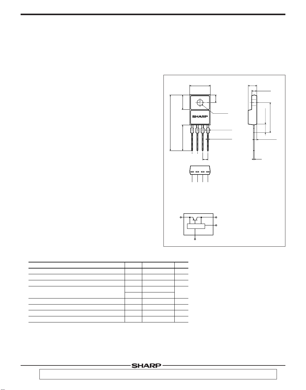
■ Outline Dimensions
10.2MAX
7.4±0.2
PQ7RV4
29.1MAX
13.5MIN
●1 ●2 ●3 ●4
Internal connection diagram
1
Control circuit
3
φ3.2±0.1
4-1.4
4-0.6
3-(2.54)
2
4
3.6±0.2
+0.3
-0
+0.2
-0.1
(Unit : mm)
4.5±0.2
2.8±0.2
4.8MAX
15.6±0.5
(1.5)
(0.5)
1 DC input (VIN)
2 DC output (V
3 GND
4 Output adjustment
terminal (V
O)
ADJ)
■ Absolute Maximum Ratings
*1
Input voltage
*1
ON/OFF control terminal voltage
Output current
*2
Power dissipation
*3
Junction temperature
Operating temperature
Storage temperature
Soldering temperature
*1
All are open except GND and applicable terminals.
*2
P
D1
: No heat sink, PD2: With infinite heat sink
*3
Overheat protection may operate at 125=<T
“ In the absence of confirmation by device specification sheets,SHARP takes no responsibility for any defects that may occur in equipment using any SHARP devices
shown in catalogs,data books,etc.Contact SHARP in order to obtain the latest version of the device specification sheets before using any SHARP's device. ”
Parameter Symbol Rating Unit
V
IN
V
ADJ
I
O
P
D1
P
D2
T
j
T
opr
-20 to +80
T
stg
-40 to +150
T
sol
260 (For 10s)
j
=<150˚C.
(Ta=25˚C)
10
5
4.6
1.8
18
150
V
V
A
W
˚C
˚C
˚C
˚C
· Please refer to the chapter“ Handling Precautions ”.
Page 2
Low Power-Loss Voltage Regulators PQ7RV4
■ Electrical Characteristics
(Unless otherwise specified, conditions shall be VIN=5V,VO=3.3V(R1=2kΩ),Io=2.0A,Ta=25˚C)
Parameter Symbol Conditions
Input voltage
Output voltage
Load regulation
Line regulation
Reference voltage
Temperature coefficient of reference voltage
Ripple rejection
Dropout voltage(1)
Dropout voltage(2)
Quiescent current
*4
Input voltage shall be the value when output voltage is 95% in comparison with the initial value.
V
RegL
R
V
TCV
RR
V
Vi-
V
eg
i-O(1)
I
IN
O
I
ref
ref
O(2)
q
O
=5mA to 4.6A
I
IN
=4 to 10V
V
j
=0 to125˚C
T
*4
, IO=4.0A
*4
, IO=4.6A
O
=0A
I
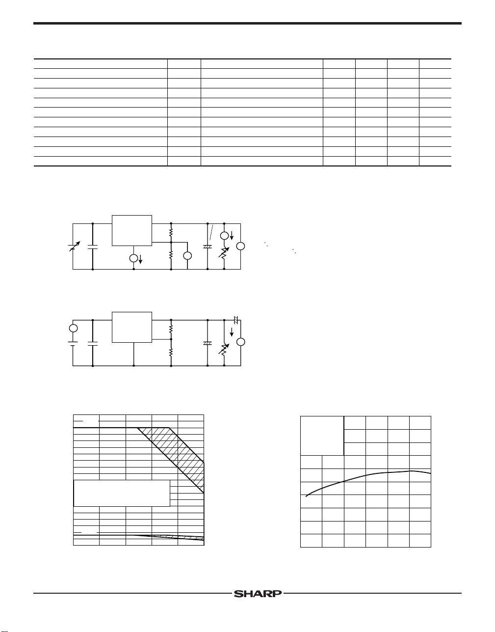
Fig.1 Test Circuit
V
IN
0.33µF
●2●1
R
2
●4
●3
R
A
Iq2kΩ
V
1
ref
V
47µF
+
V
O
O
I
A
R
V
=1.25
V
[R
L
Fig.2 Test circuit for Ripple Rejection
e
i
~
V
IN
0.33µF
●2●1
R
2
●4
●3
2kΩ
47µF
R
1
+
f=120Hz (sine wave)
I
O
+
R
e
VO=3V
e
o
V
V
~
I
L
RR=20 log (e
-
-
-
-
o
=V
ref X
(1+R2/R1)
X
(1+R2/R1)
1
=2kΩ,Vre=1.25V]
i
=0.5V
rms
IN
=5V (R1=2kΩ)
O
=0.5A
i/eo
7.0
2.0
2.5
0.5
1.0
17
UnitMAX.TYP.
V
V
%
%
V
%/˚C
dB
-
V
V
mA
MIN.
3.0
1.5
-
-
1.225
-
45
-
-
-
)
-
-
0.5
0.5
1.25
±0.01
55
-
-
-
10.0
1.275
Fig.3 Power Dissipation vs. Ambient
Temperature
20
P
D2
15
(W)
D
10
PD1 :No heat sink
P
D2
:With infinite heat sink
5
Power dissipation P
P
D1
0
-20 0
Ambient temperature Ta (˚C)
Note) Oblique line portion:Overheat protection may operate
in this area.
20 40 60 80
Fig.4 Reference Voltage Deviation vs.
Junction Temperature
5
V
IN
=5V
4
O
=3.3V
V
(mV)
O
1
=2kΩ
R
3
O
=2A
I
2
1
0
-1
-2
-3
-4
Reference voltage deviation ∆V
-5
-25 0 25 50 75 100 125
Junction temperature Tj (˚C)
Page 3

Low Power-Loss Voltage Regulators PQ7RV4
Fig.5 Relative Output Voltage vs. Output
Current (Typical Value)
100
80
60
40
20
Relative output voltage (%)
0
0 2.0 4.0 6.0 8.0 1.0
Output current IO (A)
Fig.7 Circuit Operating Current vs. Input
Voltage
a
=25˚C
T
120
(mA)
100
BIAS
L
=0.72Ω
50
Curcuit operating current I
0
052413
Input voltage V
R
L
=1.65Ω
R
L
=∞
R
IN
(V)
Fig.6 Output Voltage vs. Input Voltage
4
a =25˚C
T
3
2
1
Output voltage VO (V)
0
012345
L=1.65Ω
R
L=∞
R
L=0.72Ω
R
Input voltage VIN (V)
Fig.8 Dropout Voltage vs. Junction
Temperature
1.0
V
O
=3.3V
1
=2kΩ
R
0.8
(V)
-O
i
0.6
I
O
I
O
=4.6A
=4A
0.4
Dropout voltage V
0.2
0
-25 0 5025 10075 125
Junction temperature Tj (˚C)
Fig.9 Quiescent Current vs. Junction
Temperature
20
V
IN
=5
18
O
=3.3V
V
1
=2kΩ
R
16
O
=0A
I
(mA)
14
q
12
10
8
6
4
Quiescent current I
2
0
-25 0 25 50 75 100 125
Junction temperature Tj (˚C)
Fig.10 Ripple Rejection vs. Input Ripple
Frequency
100
80
60
40
20
Ripple rejection RR (dB)
VIN=5V
Io=0.5A
e
i=0.5Vrms
0
0.1 101 100
Input ripple frequency f
(kHz)
Page 4

Low Power-Loss Voltage Regulators PQ7RV4
■ Standard Connection
D
1
V
V
IN
●1
C
IN
●2
●4
●3
+
R
2
C
ref
390Ω
1
R
to5kΩ
+
C
O
D1 : This device is necessary to protect the element from damage when reverse voltage may be applied to the regulator in case of
input short-circuiting.
Cref : This device is necessary when it is required to enhance the ripple rejection or to delay the output start-up time. Otherwise, it
is not necessary.
(Care must be taken since Cref may raise the gain,facilitating oscillation.)
* The output start-up time si proportional to Cref X R2.
CIN,CO : Be sure to mount the devices CIN and CO as close to the device terminal as possible so as to prevent oscillation.
The standard specification of CIN and CO is 0.33µF and 47µF, respectively. However, adjust them as necessary after
checking.
R1,R2 : These devices are necessary to set the output voltage. The output voltage VO is given by the following formula:
VO=Vref X (1+R2/R1)
(Vref is 1.25V TYP)
The standard value of R1 is 2kΩ. But value up to 390Ω to 5kΩ does not cause any trouble.
O
Load
■ Asjustment of Output Voltage
Output voltage is able to set (1.5V to 7V) when resistors R1,R2 are attached to ™, £, ¢ terminals. As for the external
resistors to set output voltage, refer to the following figure.
2
+
V
ref
4
3
■ ON/OFF Operation
D1
VIN
●1
CIN
●2
R2
●4
●3
R1
VADJ
V
O
2
R
VO=Vref X (1+R2/R1)
R
1
D
2
+
R3
CO
High : Output OFF
VC
Low : Output ON
X (1+R
=1.25
1
=2kΩ,Vref =1.25V)
(R
VO
RL
2
/2000)
ADJ
V
R
R1
Equivalent Circuit
in OFF-state
D2
2
RL
RD
VO’
Page 5

Low Power-Loss Voltage Regulators PQ7RV4
ON/OFF operation is available by mounting externally D2 and R3.
When VADJ is forcibly raised above Vref (1.25V TYP) by applying the external signal,the output is turned off (pass transistor of
regulator is turned off). When the output is OFF, VADJ must be higher than Vref MAX., and at the same time must be lower than
maximum rating 5V.
In OFF-state, the load current flows to RL from VADJ through R2. Therefore the value of R2 must be as high as possible.
In OFF state, as shown below,voltage
VO'=VADJ X RL/ (RL+R2)
occurs at the load. OFF-state equivalent circuit R1 up to 5kΩ is allowed.
Select as high value of RL and R2 as possible in thisrange. In some case, as output voltage is getting lower (VO<1V), impedance of load
resistance rises. In such condition, it is sometimes impossible to obtain the minimum value of VO'. So add the dummy resistance
indicated by RD in the figure to the circuit parallel to the load.
 Loading...