

Page 1
Low Power-Loss Voltage Regulators PQ30RV31
PQ30RV31
Variable Output Low Power-Loss Voltage Regulator
■ Features
¡Maximum output current : 3A
¡Compact resin full-mold package.
¡Low power-loss (Dropout voltage : MAX.0.5V)
¡Variable output voltage (setting range : 1.5 to 30V)
¡Built-in ON/OFF control function.
■ Applications
¡Power supply for print concentration control of word processors
¡Series power supply for motors and solenoid
¡Series power supply for VCRs and TVs
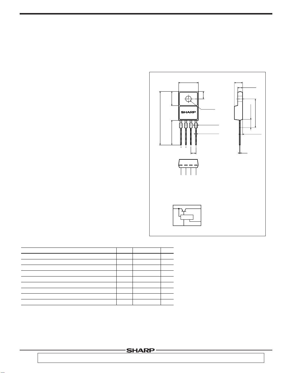
■ Outline Dimensions
10.2MAX
7.4±0.2
PQ30RV31
29.1MAX
13.5MIN
●1 ●2 ●3 ●4
Internal connection diagram
1
Specific IC
3
φ3.2±0.1
4-1.4
4-0.6
3-(2.54)
2
4
3.6±0.2
+0.3
-0
+0.2
-0.1
1 DC input (VIN)
2 DC output (V
3 GND
4 Output voltage
minute
adjustment
terminal (V
4.5±0.2
O)
ADJ)
(Unit : mm)
2.8±0.2
4.8MAX
15.6±0.5
(1.5)
(0.5)
■ Absolute Maximum Ratings
*1
*1
*2
*1
*2
Parameter Symbol Rating Unit
Input voltage
Output adjustment terminal voltage
Output current
Power dissipation (No heat sink)
Power dissipation (With infinite heat sink)
Junction temperature
Operating temperature
Storage temperature
Soldering temperature
All are open except GND and applicable terminals.
Overheat protection function may operate at 125=<T
“ In the absence of confirmation by device specification sheets,SHARP takes no responsibility for any defects that may occur in equipment using any SHARP devices
shown in catalogs,data books,etc.Contact SHARP in order to obtain the latest version of the device specification sheets before using any SHARP's device. ”
j
=<150˚C.
V
IN
V
ADJ
I
O
P
D1
P
D2
T
j
T
opr
T
stg
T
sol
35
7
3
2.0
20
150
-20 to +80
-40 to +150
260 (For 10s)
(Ta=25˚C)
V
V
A
W
W
˚C
˚C
˚C
˚C
· Please refer to the chapter“ Handling Precautions ”.
Page 2
Low Power-Loss Voltage Regulators PQ30RV31
■ Electrical Characteristics
(Unless otherwise specified, condition shall be VIN=12V, Vo=10V, Io=1.5A, R1=390Ω, Ta=25˚C)
Parameter Symbol Conditions
Input voltage
output voltage
Load regulation
Line regulation
Ripple rejection
Reference voltage
Temperature coefficient of reference voltage
Dropout voltage
Quiescent current
*3
Input voltage shall be the value when output voltage is 95% in comparison with the initial value.
V
V
RegL
R
RR
V
TcV
Vi-
IN
O
eg
I
ref
ref
O
I
q
O
=5mA
to
I
IN
=11 to 21V, IO=0.5mA
V
Refer to Fig. 2
j
=0 to 125˚C,IO=5mA
T
*3
, IO=3A
*3
, IO=2A
O
=0
I
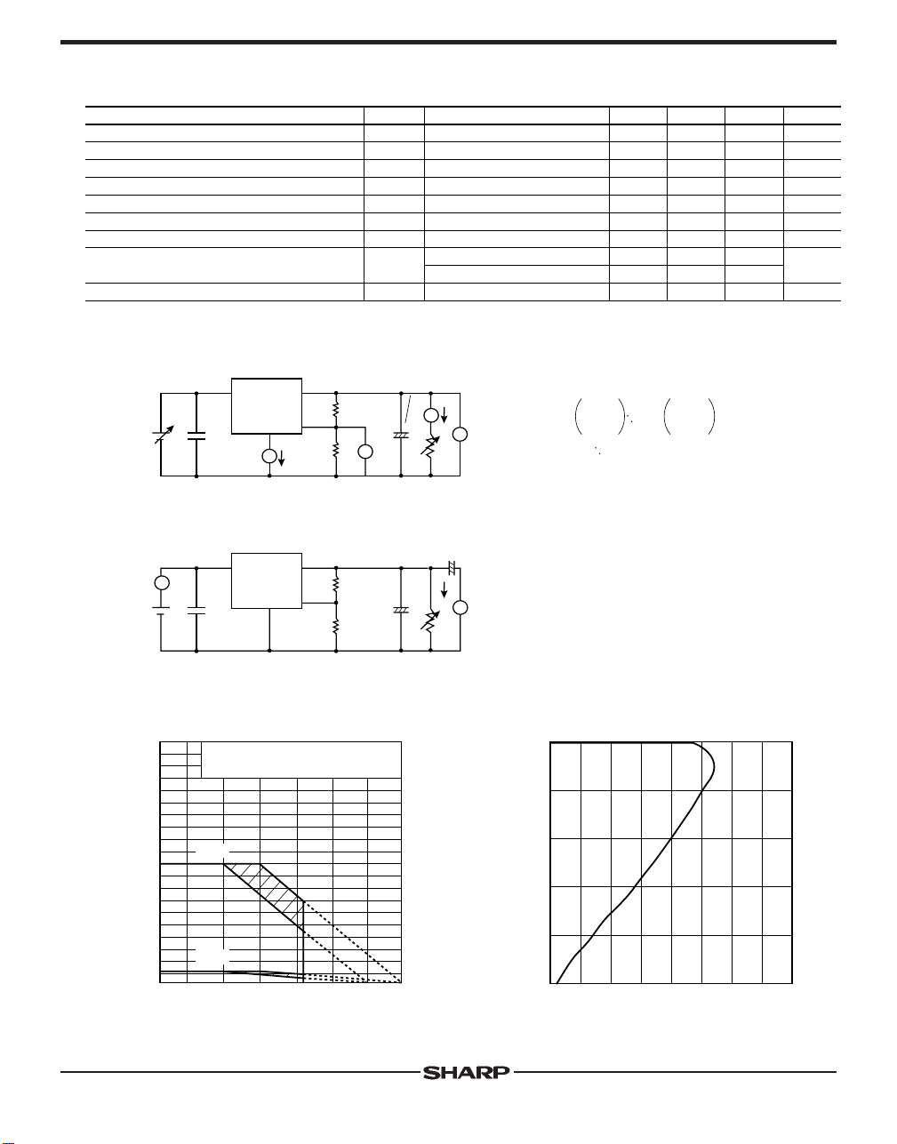
Fig.1 Test Circuit
V
IN
0.33µF
●3
A
●2●1
R
●4
R
Iq390Ω
2
V
1
ref
V
47µF
+
V
O
I
O
A
V
R
L
Fig.2 Test Circuit of Ripple Rejection
e
i
~
V
IN
0.33µF
●2●1
R
2
●4
●3
390Ω
47µF
R
1
+
O
I
+
e
o
V
~
R
L
-
-
3A
-
V
O
=V
ref
X 1+ -------- =1.25X 1 + --------
[R1=390Ω, V
IO=0.5A, VIN=12V, VO=10V
f=120Hz (sine wave)
i
=0.5V
e
RR=20 log (ei/eo)
rms
ref
=1.25V]
UnitMAX.TYP.MIN.
4.5
1.5
-
-
45
1.225
-
-
-
-
R
2
R
1
-
-
0.5
0.5
70
1.25
±1.0
0.3
0.2
-
R
R
35
30
2.0
2.5
-
1.275
-
1.0
0.5
7
2
1
V
V
%
%
dB
V
%/˚C
V
mA
Fig.3 Power Dissipation vs. Ambient
Temperature
40
(W)
D
30
20
Power dissipation P
10
0
Note) Oblique line portion:Overheat protection may operate in
this area.
D1
:No heat sink
P
D2
:With infinite heat sink
P
P
D2
P
D1
0 50 100 150
Ambient temperature Ta (˚C)
Fig.4 Overcurrent Protection
Characteristics (Typical Value)
100
80
60
40
Relative output voltage (%)
20
0
4.0 5.0 6.0 7.0 8.01.0 2.0 3.00
Output current IO (A)
Page 3

Low Power-Loss Voltage Regulators PQ30RV31
Fig. 5 Output Voltage Adjustment
Characteristics(Typical value)
30
1 390Ω
R
25
20
15
10
Output voltage VO (V)
5
0
1
10
2
10
3
10
4
10
5
10
R2 (Ω)
Fig.7 Dropout Voltage vs. Junction
Temperature
0.7
0.6
(V)
0.5
-O
i
0.4
0.3
0.2
Dropout voltage V
0.1
0
-25 0 25 50
Junction temperature Tj (˚C)
0.5A
R
1
IN
V
O
I
=390Ω,R2=2.7kΩ
; 0.95V
O
=3A
2A
1A
100 125
75
Fig.9 Ripple Rejection vs. Output Current
90
Fig.6 Output Voltage vs. Input Voltage
15
R1=390Ω,R2=2.7kΩ,Tj=25˚C
10
R
L=∞
5
Output voltage VO (V)
R
L=3.3Ω
0
0
5101520
Input voltage VIN (V)
Fig.8 Ripple Rejection vs. Input Ripple
Frequency
90
80
C
ref=3.3µF
70
No C
60
ref
50
40
30
20
Ripple rejection RR (dB)
j=25˚C,VIN=12V
T
10
R1=390Ω,R2=2.7kΩ
IO=0.5A,ei=0.5Vrms
0
0.1 1 10 100 1000
Input ripple frequency f (kHz)
Fig.10 Output Peak Current vs. Dropout
Voltage(Typical)
7
ref
=3.3µF
C
80
No C
70
ref
60
Ripple rejection RR (dB)
50
Tj=25˚C
R
1
=390Ω,R2=2.7kΩ
V
IN
40
=12V,ei=0.5V
rms
,f=120Hz
0123
Output current I
O
(A)
6.5
(A)
OP
6
5.5
5
Output peak current I
4.5
R1=390Ω,R2=2.7kΩ,Ta=25˚C
4
01 2345678910
Dropout voltage V
i
-O
(V)
Page 4

Low Power-Loss Voltage Regulators PQ30RV31
Fig.8 Ripple Rejection vs. Input Ripple
Frequency
7
6.5
(A)
OP
6
5.5
5
Output peak current I
4.5
VIN=15V,R1=390Ω,R2=2.7kΩ
4
-25 1007550250
Dropout voltage V
i
-O
(V)
■ ON/OFF Operation
D
1
V
IN
●1
C
IN
●2
D
2
R
2
●4
●3
V
ADJ
R
R
1
D
V
V
O
R
+
R
3
C
L
O
1
2
ADJ
R
2
R
R
L
D
VO’
High:Output OFF
V
C
Low :Output ON
Equivalent Circuit
in OFF-state
¡ON/OFF operation is available by mounting externally D2 and R3.
¡When VADJ is forcibly raised above VREF (1.25V TYP) by applying the external signal, the output is turned off (pass transistor of
regulator is turned off. When the output is OFF, VADJ must be higher then VREF MAX., and at the same time must be lower than
maximum rating 7V.
In OFF-state, the load current flows to RL from VADJ through R2. Therefore the value of R2 must be as high as possible.
¡VO'=VADJ X RL/ (RL+R2)
occurs at the load. OFF-state equivalent circuit R1 up to 10kΩ is allowed. Select as high value of RL and R2 as possible in this range.
In some case, as output voltage is getting lower (VO<1V), impedance of load resistance rises. In such condition, it is sometime
impossible to obtain the minimum value of VO'. So add the dummy resistance indicated by RD in the figure to the circuit parallel to
the load.
 Loading...