

Page 1
Primary Regulators
PQ1PF1
PQ1PF1
Primary Regulator for Switching Power Supply (50W Class)
■ Features
¡5-terminal lead forming package (equivalent to TO-220)
¡Built-in oscillation circuit
(oscillation frequency : TYP. 100kHz)
¡Output for power supply : 50W class
¡Built-in overheat protection, overcurrent protection, low voltage
mulfunction prevention function
■ Applications
¡Switching power supplies for VCRs
¡Switching power supplies for word processors
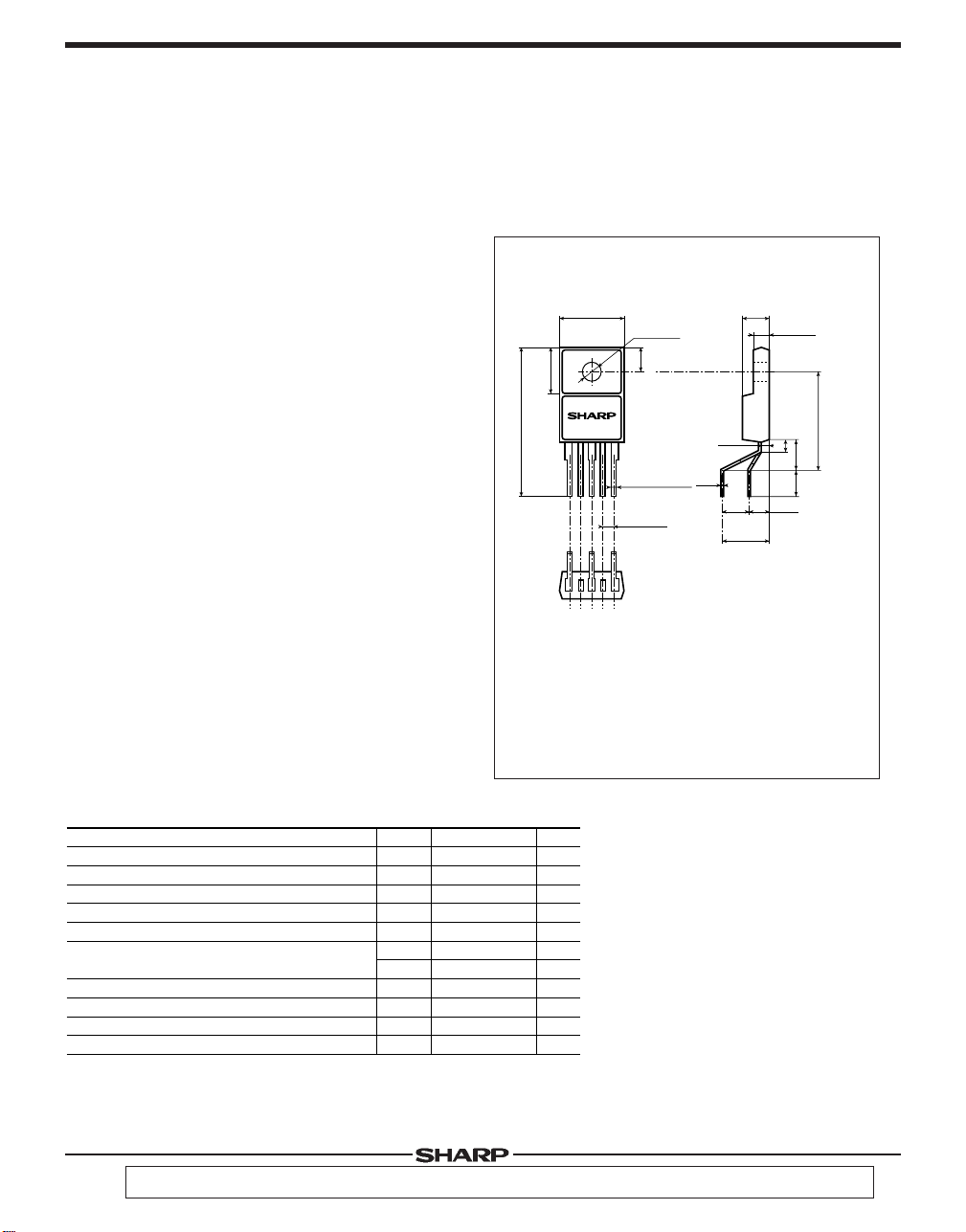
■ Outline Dimensions
10.2MAX
φ3.2±0.1
7.4±0.2
PQ1PF1
(24.6)
●1●2 ●3●4 ●5
3.6±0.2
5-0.8±0.1
4-(1.7)
(Unit : mm)
4.5±0.2
2.8±0.2
3.2±0.5
)
16.4±0.7
2.0
5.0±0.5
4.4MIN
CC
)
(1.5)
(0.5)
(5.0)
8.2±0.7
· ( ) : Typical value
· Radius of lead forming portion
R=TYP.1.0
1 Drain (V
2 GND
3 Control (CA)
4 Feed back (FB)
5 Supply voltage (V
DS
■ Absolute Maximum Ratings
Drain-GND(source)voltage
Drain current
*1
Power supply voltage
*2
FB terminal input voltage
CA terminal input current
*3
Power dissipation
*4
Junction temperature
Operating temperature
Storage temperature
Soldering temperature
*1
Voltage between V
*2
Voltage between FB terminal and GND terminal.
*3
P
D1
:No heat sink, PD2:With infinite heat sink
*4
Overheat protection may operate at 125=<Tj=<150˚C
“ In the absence of confirmation by device specification sheets,SHARP takes no responsibility for any defects that may occur in equipment using any SHARP devices
shown in catalogs,data books,etc.Contact SHARP in order to obtain the latest version of the device specification sheets before using any SHARP's device. ”
Parameter Symbol Rating Unit
CC
terminal and GND terminal.
V
DS
I
D
V
CC
V
FB
I
CA
P
D1
P
D2
T
j
T
opr
T
stg
T
sol
500
4.5
35
4
2
2
20
150
-20 to +80
-40 to +150
260 (For 10s)
(Ta=25˚C)
V
A
V
V
mA
W
W
˚C
˚C
˚C
˚C
· Please refer to the chapter“ Handling Precautions ”.
Page 2
Primary Regulators
PQ1PF1
■ Electrical Characteristics
Drain-source onstate resistance
Drain-source leakage current
Oscillation frequency
Temperature change in oscillation frequency
Maximum duty
FB threshold voltage
FB current
CA threshold voltage
CA sink current
Overcurrent detecting level
Operation starting voltage
Operation stopping voltage
Stand-by current
Output OFF-mode consumption current
Output-operating mode consumption current
Charging current
Parameter Symbol Conditions
Fig. 1 Test circuit
C
IN
100µF 0.01µF
A
+
V
CC
V
FB
●5 ●1
PQ1PF1
●4
A
(Unless otherwise specified, conditions shall be VDS=10V,Vcc=18V,VCA=OPEN,VFB=2.2V, RL=56Ω, Ta=25˚C)
UnitMAX.TYP.MIN.
R
DS (on)
I
DSS
fo
∆fo
MAX
D
V
V
V
FB(OCP)
I
V
CAL
V
CAH
V
CA(ON/OFF)
CA(OVP)
V
I
CAIN
I
D(OCP)
V
CC(ON)
V
CC(OFF)
I
CC(ST)
I
CC(OFF)
I
CC(OP)
I
CA(CHG)
●2
FBL
FBH
FB
●3
ID=2A
DS
=500V,Vcc=7V
V
CA
=GND,VFB=GND
V
j
=0 to 125˚C
T
Duty=0%
MAX
Duty=D
VCA=6V
FB
=GND
V
Duty=0%
MAX
Duty=D
VFB=1V,VCA=6V
DS
=OPEN,VFB=OPEN
V
DS
=OPEN,VFB=OPEN
V
DS
=OPEN,Vcc=14V,
V
FB
=OPEN
V
DS
=OPEN,VCA=GND
V
FB
=OPEN
V
CA
=GND,VFB=OPEN
V
A A
V
CA
-
1.2
-
90
100
-
42
2.6
-800
0.49
7.2
20
15.5
8.5
-15
R
L
V
DS
±5
45
-
0.9
-
1.8
2.8
-620
-
0.9
-
1.8
0.6
7.7
36
-
2.5
17.0
9.3
-
100
-
0.6
-
10
-10
1.5
-
250
110
50
3.1
-440
0.74
8.2
52
18.5
10.1
150
1.8
18
-5
Ω
µA
kHz
%
%
V
-
V
-
V
µA
V
-
V
-
V
V
µA
A
-
V
V
µA
mA
mA
µA
Page 3
Primary Regulators
,,
,,
PQ1PF1
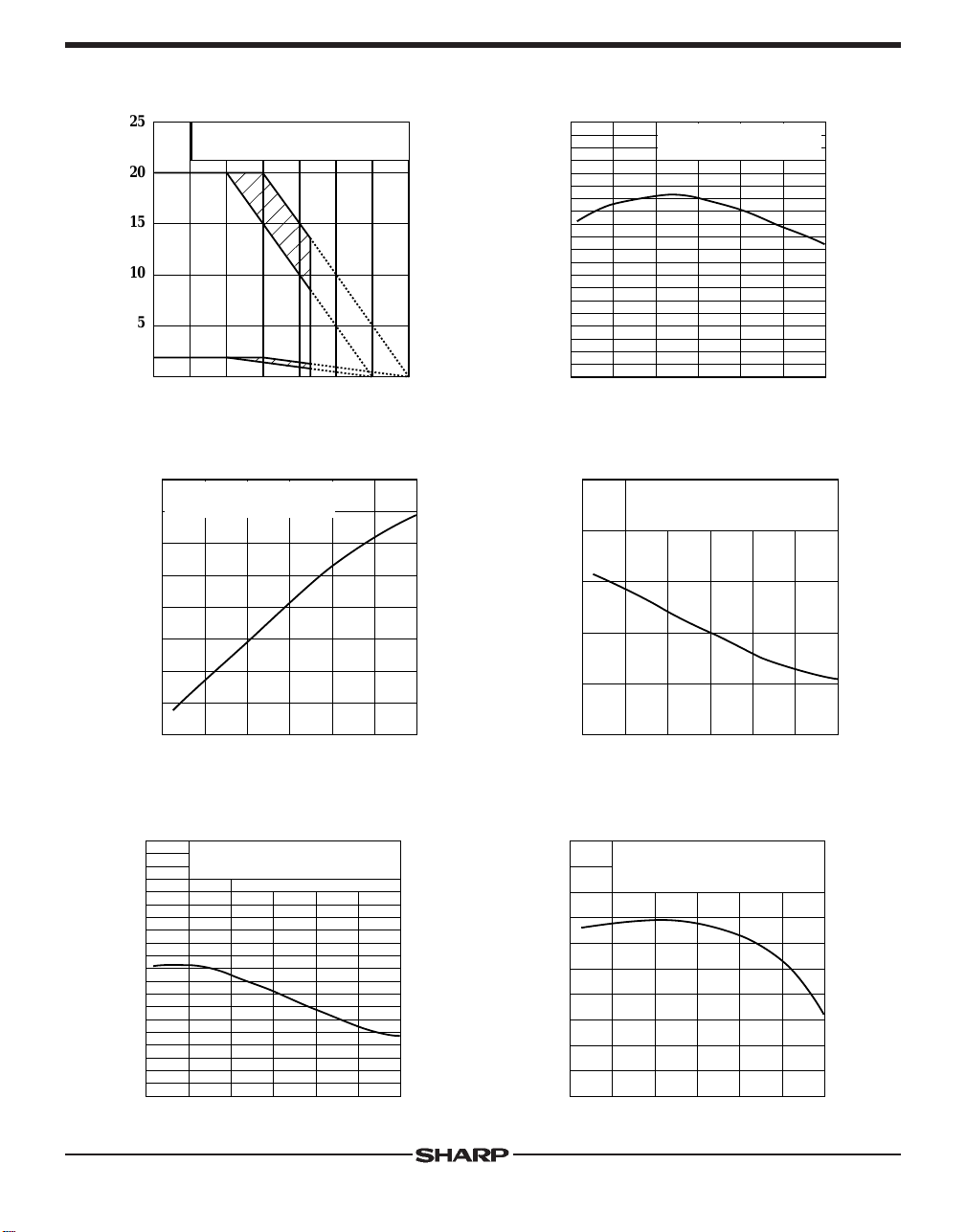
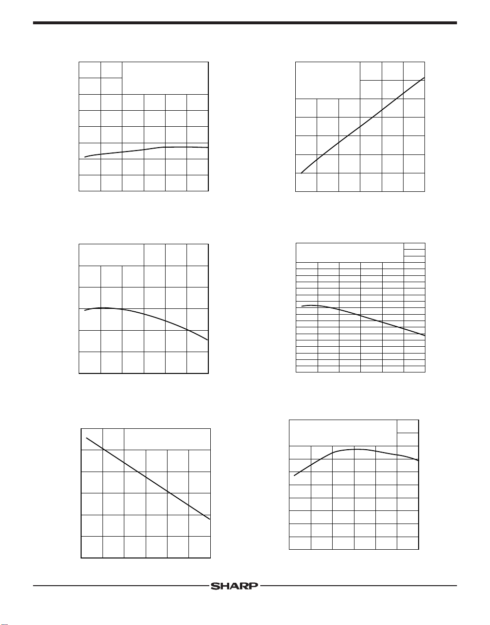
Fig. 2 Power Dissipation vs. Ambient
(W)
D
Power dissipation P
Fig. 4 Operation Starting Voltage vs.
17.6
(V)
17.5
CC (ON )
17.4
17.3
17.2
17.1
17.0
16.9
Operation starting voltage V
16.8
Fig. 6 Oscillation Frequency vs. Junction
110
105
100
95
Oscillation frequency fO (kHz)
90
Temperature
25
20
15
10
5
0
-20 0 50 80 100 150
D1
:No heat sink
P
P
D2
:With infinite heat sink
P
D2
P
D1
Ambient temperature Ta (˚C)
Junction Temperature
VCA=OPEN
V
FB=OPEN, VDS=OPEN
-25 0
25 50 75 100 125
Junction temperature T
j
(˚C)
Temperature
VCC=18V,VCA=OPEN
V
FB=2.2V,VDS=10V,RL=56Ω
-25 0
25 50 75 100 125
Junction temperature T
j (˚C)
Fig. 3 Stand-by Current vs. Junction
Temperature
100
(µA)
95
CC (ST )
90
85
Stand-by current I
80
-25 0
VCC=14V , VCA=OPEN
V
FB
=OPEN, VDS=OPEN
25 50 75 100 125
Junction temperature T
j
(˚C)
Fig. 5 Output-Operating Mode Consumption
Current vs. Junction Temperature
12
VCC=18V,VCA=OPEN
V
FB
=2.2V,VDS=10V,RL=56Ω
11
(mA)
10
CC(OP)
9
current I
8
Output-operating mode consumption
7
-25 0
25 50 75 100 125
Junction temperature T
j
(˚C)
Fig. 7 Maximum Duty vs. Junction
Temperature
47.0
46.5
(%)
46.0
MAX
45.5
45.0
44.5
44.0
43.5
Maximum duty D
43.0
42.5
42.0
-25 0
VCC=18V,VCA=OPEN
V
FB
=2.2V,VDS=10V,RL=56Ω
25 50 75 100 125
Junction temperature T
j
(˚C)
Page 4
Primary Regulators
PQ1PF1
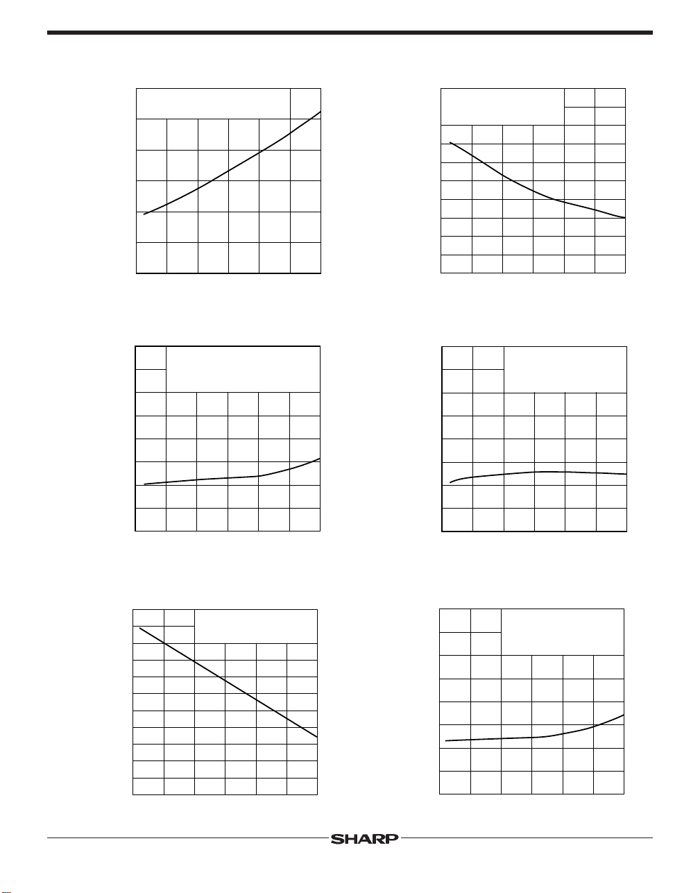
Fig.8 Drain-soure onstate resistance vs.
Junction Temperature
3.0
VCC=18V,VCA=OPEN
FB=2.2V,VDS=10V,ID=2A
V
2.5
2.0
1.5
1.0
0.5
0
Drain-source onstate resistance RDS(ON) (Ω)
-25 0
25 50 75 100 125
Junction temperature T
j (˚C)
Fig.10 FB Threshold Voltage vs. Junction
Temperature
1.20
VCC=18V,VCA=OPEN
V
DS=10V,RL=56Ω
25 50 75 100 125
Junction temperature T
j (˚C)
FB threshold voltage VFBL (V)
1.15
1.10
1.05
1.00
0.95
0.90
0.85
0.80
-25 0
Fig.9 Overcurrent Detecting Level vs.
Junction Temperature
3.0
CC
=18V,VCA=OPEN
V
(A)
2.9
FB
=2.2V,VDS=10V
V
2.8
D (OCP)
2.7
2.6
2.5
2.4
2.3
2.2
2.1
Overcurrent detecting level I
2.0
-25 0
25 50 75 100 125
Junction temperature Tj (˚C)
Fig.11 FB Threshold Voltage vs. Junction
Temperature
2.10
2.05
(V)
2.00
FBH
1.95
1.90
1.85
1.80
1.75
FB threshold voltage V
1.70
-25 0
Junction temperature Tj (˚C)
VCC=18V,VCA=OPEN
V
DS
=10V,RL=56Ω
25 50 75 100 125
Fig.12 CA Threshold Voltage vs. Junction
Temperature
0.75
0.70
(V)
0.65
0.60
CA(ON/OFF)
0.55
0.50
0.45
0.40
0.35
0.30
CA threshold voltage V
0.25
0.20
-25 0
Junction temperature Tj (˚C)
CC
=18V,VCA=OPEN
V
V
DS
=10V,RL=56Ω
25 50 75 100 125
Fig.13 CA Threshold Voltage vs. Junction
Temperature
1.20
1.15
(V)
1.10
CA L
1.05
1.00
0.95
0.90
0.85
CA threshold voltage V
0.80
-25 0
Junction temperature Tj (˚C)
V
CC
=18V,VFB=2.2V
V
DS
=10V,RL=56Ω
25 50 75 100 125
Page 5
Primary Regulators PQ1PF1
Fig.14 CA Threshold Voltage vs. Junction
Temperature
2.10
CC
=18V,VFB=2.2V
V
V
DS
=10V,RL=56Ω
(V)
CA H
2.05
2.00
1.95
1.90
1.85
1.80
CA threshold voltage V
1.75
1.70
-25 0
25 50 75 100 125
Junction temperature Tj (˚C)
Fig.16 FB Threshold Voltage vs. Junction
Temperature
3.00
CC
=18V,VCA=6V
V
DS
=10V,RL=56Ω
V
2.95
(V)
2.90
FB(OCP)
2.85
Fig.15 CA Threshold Voltage vs. Junction
Temperature
8.6
V
CC
=18V,VFB=2.2V
8.4
DS
=10V,RL=56Ω
V
(V)
8.2
CA(OVP)
8.0
7.8
7.6
7.4
CA threshold voltage V
7.2
-25 0
25 50 75 100 125
Junction temperature Tj (˚C)
Fig.17 CA Sink Current vs. Junction
Temperature
50
VCC=18V,VCA=6V
V
DS=10V,RL=56Ω,VFB=1V
45
40
2.80
2.75
FB threshold voltage V
2.70
-25 0
25 50 75 100 125
Junction temperature Tj (˚C)
Fig.18 FB Current vs. Junction
Temperature
FB current IFB (µA)
-700
-650
-600
-550
-500
-450
-400
-25 0
Junction temperature T
VCC=18V,VCA=OPEN
FB=GND,VDS=OPEN
V
25 50 75 100 125
j (˚C)
35
CA sink current ICA(IN) (µA)
30
-25 0
25 50 75 100 125
Junction temperature T
j (˚C)
Fig.19 Charging Current vs. Junction
Temperature
-10.5
CC
=18V,VCA=GND
V
-10.3
V
FB
=OPEN,VDS=10V,RL=56Ω
-10.1
(µA)
-9.9
CA(CHG)
-9.7
-9.5
-9.3
-9.1
-8.9
Charging current I
-8.7
-8.5
-25 0
25 50 75 100 125
Junction temperature Tj (˚C)
Page 6

Primary Regulators
PQ1PF1
Fig.20 Output-OFF Mode Consumption
Current vs. Junction Temperature
0.08
(mA)
0.75
CC(OFF)
0.70
0.65
0.60
0.55
0.50
0.45
0.40
0.35
0.30
Output-OFF mode consumption current I
-25 0
VCC=18V,VCA=GND
V
FB
=OPEN,VDS=OPEN
25 50 75 100 125
Junction temperature T
j (˚C)
Fig.21 Operation Stopping Voltage vs.
Junction Temperature
9.40
(V)
9.35
CC(OFF)
9.30
9.25
9.20
9.15
Operation stopping voltage V
9.10
-25 0
V
CA
=GND
V
FB
=OPEN,VDS=OPEN
25 50 75 100 125
Junction temperture T
j
(˚C)
■ Block Diagram
Overheat
detection
Overload cut-off
voltage circuit
FB
circuit
CA V
←
Low voltage
malfunction
prevention circuit
Cut-off voltage
detecting circuit
OFF voltage
detecting circuit
O S C
PWM
+
-
-
-
DET
V
Constant
voltage
source
DS
GND
CC
R
Q
S
Drive
circuit
Overcurrent
detection
circuit
Page 7

Primary Regulators
PQ1PF1
■ Description for Each Operation
1. Low voltage mulfunction prevention circuit
This device has a built-in low voltage malfunction prevention circuit to prevent malfuncting when power supply voltage Vcc
becomes as low as starting time. When power supply voltage comes up to operation starting voltageVCC( ON)17.0V TYP., IC will
start to operate. When power supply voltage falls short of operation stopping voltageVCC(OFF)9.3V TYP., IC will stop operating, and
output is shut down.
Before starting power supplies or after stopping operation, applying current to Vcc terminal is stood for stand-by current ICC(ST), and
it is kept at 100µA TYP. (Vcc=14V).
2. Oscillator
IC has a built-in oscillator, and oscillation frequncy is fixed at 100kHz TYP.
3. CA terminal
CA terminal can be connected to capacitor CA, and it enables to perform various functions such as soft start function, overcurrent
protection function, overvoltage protection function, and ON/OFF control function.
3-1 Soft start function
Soft start circuit is shown in Fig.1. When voltage Vcc is supplied, CA terminal voltage VCA starts rising, charging a capacitor CA
with charge current from CA terminal(10µA TYP.). According to rising CA teminal voltage VCA, output pulse width becomes
gradually wider, and it may cause soft start.
ON duty D of output pulse width is as follows.
D=0% at VCA=0.9V TYP.
D=Dmax=45% at VCA=1.8V TYP.
During normal operaion, VCA is clamped at 3.6V by the internal circuit of IC.
C
A
V
CA
35
3.6V
OSC
F
B
4
Fig.1 Soft Start Circuit
CC
←
10µA
+
PWM
-
-
-
Page 8

Primary Regulators
PQ1PF1
3-2 Overcurrent protection function
Overcurrent protection circuit is shown in Fig.2. Fig.3 shows timing chart of OFF control process after detecting overcurrent.
First, drain current of MOS-FET (which is built-in device) is getting high due to overcurrent. When it comes up to overcurrent
detection level ID(OCP)=2.5A, overcurrent protection circuit will operate and minimize output pulse width to minimum duty by pulseby-pulse. Minimizing output pulse width makes output voltage lower. As output voltage is lowered, collector-emitter voltage of
PC1 will be turned OFF and FB voltage VFB will be high. When VFB comes up to threshold voltage of overload shut-down VFB(OCP)
2.8V, CA voltage VCA will be released from clamped voltage 3.6V and the capacitor CA which is connected to CA terminal will be
charged again by 10µA of charge current. When VCA increases to CA threshold voltageVCA (OVP) 7.7V, internal constant voltage
supply of IC becomes OFF-state and maintain shut-down state. To maintain output shut-down condition, 0.3mA (Vcc=11V) TYP.
is required. To restart, Vcc needs to be lowered less then operation stopping voltageVCC(OFF) 9.3V by applying input voltage again.
Fig.2 Overcurrent Protection Circuit
Fig.3 Timing Chart Overcurrent Protection
CA
PC1
35
4
PQ1PF1
1
Output current
2
3.6V
D
DMIN
V
V
MAX
VFB (OCP)
FB
CA
0
2.8V
V
Overcurrent
detection
CA (OVP)
7.7V
Overload shut-down
Page 9

Primary Regulators
PQ1PF1
3-3 Overvoltage protection function
Fig.4 shows overvoltage protection circuit. Photocoupler PC2 becomes ON-state when output voltage is in overvoltage condition.
When PC2 is ON-state, current from Vcc via resistor R charges capacitor CA and CA voltage VCA increases. When VCA reaches CA
threshold voltageVCA( OVP) 7.7V, internal constant voltage supply of IC becomes OFF-state and maintain shut-down state. To maintain
output shut-down condition, 0.3mA (Vcc=11V) TYP. is reguired. To restart, Vcc needs to be lowered less than operation stopping
voltage VCC(OFF) 9.3V by applying input voltage again.
Fig.4 Overvoltage Protection Cricuit
R
PC
2
C
A
5
V
CA
CC
PQ1PF1
3
3-4 ON/OFF control function
IC operation can be stopped and output voltage can be OFF-state by lowering CA voltage VCA less than 0.6V TYP. Fig.5 shows ON/
OFF control circuit. When transistor Q1 becomes ON-state by external signal and VCA is less than 0.6V, output turns off. Output is
ON-state again by soft start function which is caused by Q1 OFF.
Fig. 5 ON/OFF Control Function
3
Q
1
C
A
CA
PQ1PF1
Page 10

Primary Regulators
4. FB-terminal
Fig.6 shows circuit example of feedback signal input circuit for fixed output voltage.
Fig.6
+
V
CC
GND V
R
C
Output voltage is controlled by connecting photocoupler PC1 between FB-terminal and GND terminal . When output voltage or
transmisslon waveform is unstable, connect C&R on both sides of PC1 to reduce gain of control system.
5
21
DS
PQ1PF1
43
FB
CA
V
PC
1
PC
+
1
PQ1PF1
5. Overcurrent detection circuit
This module detects drain current ID of MOS-FET, and minimize output pulse width by pulse-by-pulse at ID=2.5A TYP.
6. Overheat protection circuit
Overheat protection circuit starts to operate when internal temperature of IC is at 140˚C TYP. CA voltage VCA will be released from
clamped voltage 3.6V and the capacitor CA which is connected to CA terminal will be charged again by 10µA of charge current.
When VCA increases to CA threshold voltageVCA (OVP) 7.7V, internal constant voltage supply of IC becomes OFF-state and maintain
shut-down state. To maintain output shut-down condition, 0.3mA (Vcc=11V) TYP. is required. Output shut-down condition is
maintained even if lowering internal temperature of IC. To restart, Vcc needs to be lowered less than 9.3V by applying input voltage
again.
Page 11

Primary Regulators
■ Precautions in Designing
1 Starting circuit
Fig.7 Diagram of Starting Circuit and It's Peripheral Portion
V
IN
DC
R
9
PQ1PF1
D
6
5
2
CC
V
GND1V
PQ1PF1
DS
+
C
10
Auxiliary winding
1-1 Setting starting resistance
Concerning stand-by current (0.15mA) MAX. and *starting time of power supply, the value of starting resistor R9 is obtained
by the following equation.
*For ex.) during 0.5s, C10 is charged to the level of operation starting voltage (18.5V) MAX.
R9= (VIN(DC)- VCC(ON)) / [0.15X10⁻³+(18.5XC10)/0.5]
VIN(DC) : DC input voltage
(Minimum input voltage which is necessary for IC to start operation ex. 70VACX 2=99VDC)
√
VCC(ON) : Operation starting voltage of IC (18.5V MAX.)
When IC start to operate, current to VCC terminal increases. The current is supplied by an auxiliary winding of main tramsformer.
After rectification of auxiliary winding, voltage (both side of C10) must be set on operation stopping voltage (VCC(OFF)=9.3V
Typ.) or more. MOS-FET driving voltage in IC is about 13V, which is applied from Vcc terminal. When Vcc is about 16.5V
or more, MOS-FET driving voltage is in optimum condition due to built-in voltage regulator circuit for driving voltage.
Page 12

Primary Regulators
1-2Extending the capacity of smoothing capacitor (C10) for auxiliary winding voltage.
After smoothing rectification of auxiliary winding (both sides of C10=Vcc), ripple voltage becomes high by turns and diameter
of auxiliary winding. When voltage falls below operation stopping voltageVCC(OFF), it may sometimes cause operating error.
In this case, it is recommended to extend C10. However, starting time becomes longer due to extending C10 because starting
time is determined by both startig resistor R9 and C10. To shorten the starting time, it is recommended to employ 2-step
rectification circuit. (Fig.8)
Fig.8 2-step Rectification Circuit
R
9
D
7
2
V
5
CC
GND
PQ1PF1
C
11
22µF
As a standard in designing, proper capacity of C11 is 10 to 47µF.
Extending the capacity of C10 in 2-step rectification circuit, current to Vcc terminal can be supplied from storaged charge in
C10 after starting operation IC.
D
6
C
10
100µF
PQ1PF1
1-3 Slow up input
During slow up start (input voltage is gradually rising), there is some cases that output is soon shut down after it starts to
operate. It is because output voltage does not exceed the rated value due to halfway of slow up starting.
A fall of output voltage during operating IC makes photocoupler PC1 (Fig.2) in voltage control system OFF-state. In that
condition, CA terminal voltage is not fixed at 3.6V, and start to rise soon after starting to operate IC. When CA terminal
voltage exceeds VCA (OVP) 7.7V, output of IC is shut down. To avoid the shud down, output must be kept the rated level,
making operation starting voltage higher. Or add a discharge circuit of capactor CA which is connected to CA terminal.
(Fig.9)
Fig. 9 Circuit Diagram for Slow Up Input
R
3
2
D
4
R
5
C
A
3 C
A
GND
PQ1PF1
Page 13

Primary Regulators
To avoid shut down, keep VCA below 7.7V, by discharging the charge of CA at R5 through D4.
To do this, use a power supply which can supply the rated power under the condition that AC input voltage is 75VAC, R3 and
R5 are designed as follows when AC input voltage is less than 75VAC.
Electric potential of both side of R5 stands for VR5.
VR5<7.7-VFD4 VFD4 : forward voltage of diode D4
When current flowing into R3 is 0.2mA,
R3= ( 2VIN (AC) [MIN]-7.7+VFD4) / (0.2X10⁻³)
√
R5= (7.7-VFD4) / (0.2X10⁻³)
VIN (AC) [MIN] : Minimum input voltage to gain the rated output
1-4 Redudtion of restarting time from shut-down state
Under the shut down condition due to overcurrent and overvoltage protection function, once supply voltage of IC (Vcc) must
be lowered below operation stopping voltage VCC (OFF) 9.3V TYP. in order to restart the power supply. Generally, AC input
voltage is once turned off. However, in cases that starting resistor R9 is connected after smoothing rectification of input
voltage(Reter to Fig. 10), it takes sometimes unexpected time to make the electric potential of Vcc drop to less than 9.3V.
This is due to storaged charge of smoothing capacitor C6.
In this case, connect a starting resistor before rectification of AC input voltage(Reter to Fig. 11). And Vcc has no influence
of storaged charge of smoothing capacitor C6 while AC input voltage is OFF. Vcc soon drop to 0V, and that can shorten the
restarting time.
PQ1PF1
Fig.10 Connecting Starting Resistor after Rectification
AC input
+
9
R
C
6
D
6
5
2
CC
V
GND1V
+
10
C
DS
VIN AC
C6
V
V
CC
Fig.11 Connecting Starting Resistor before Rectification
AC input
+
C6
R
9
5
2
CC
V
GND1V
D6
+
10
C
DS
VIN AC
VC6
V
CC
9.3V
OFF
C
T
a
A
Possible to restart after Ta
AC
OFF
Possible to restart after AC OFF
t
t
Page 14

Primary Regulators PQ1PF1
While AC input voltage is OFF, output of IC is shut down and it takes some time to restart. This is because electric potential
of IC input terminal (Vcc) is more than operation stopping voltageVCC (OFF) 9.3V Typ., and IC keeps operating.(Refer to
Fig.12)
In this case, connect the starting resistor before smoothing so that Vcc soon drops to 0V. As a result, output will not be shut
down while AC input voltage is OFF. (Refer to Fig.11)
Fig. 12 Timing Chart at OFF-state of AC Input Voltage (Connecting Starting Resistor after Rectification)
V
IN
AC
OUT
V
CC
V
9.3V
Output shut-down state
Impossible to restart possible to restart
IC operates.
AC OFF
2 Patterning to Printed Circuit Board
Patterning to a printed circuit board may cause a noise and a malfuntion. Especially for dotted line portion Fig.13, reduce the
roop area and make the pattern thick and short because high frequency current flows in that portion.
The capacitor C12 which should be connected to CA teminal must be connected as close as possible to IC, and auxitiary
winding GND must be directly connected to IC GND (do not connect by way of control system GND).
t
Fig. 13 Patterning to PCB
V
IN
+
C
6
GND
(F
G
)
GND
CAFBV
C
12
P
IC V
+
C1
C
10
Control system GND
Auxiliary winding GND
D
5
T
1
+
DS
CC
D
6
V
OUT
C
16
GND
 Loading...