

Page 1
Low Power-Loss Voltage Regulators PQ05SZ5/PQ05SZ1 Series
PQ05SZ5/PQ05SZ1 Series
Low Power-Loss Voltage Regulators (Built-in Reverse Voltage Protection Function)
■ Features
¡Low power-loss (Dropout voltage : MAX. 0.5V)
¡Surface mount type package (Equivalent to SC-63)
¡Built-in a function to prevent reverse voltage between input and
output
The diode to prevent reverse voltage between input and output is
not necessary. (When VO-I=<13V)
■ Applications
¡Portable equipment
¡Notebook PC
■ Model Line-ups
Output voltage
precision:±5%
Output voltage
precision:±2.5%
0.5A output
Output voltage
precision:±5%
Output voltage
1A output
precision:±2.5%
5V output
PQ05SZ5
PQ05SZ51
PQ05SZ1
PQ05SZ11
9V output
PQ09SZ5
PQ09SZ51
PQ09SZ1
PQ09SZ11
12V output
PQ12SZ5
PQ12SZ51
PQ12SZ1
PQ12SZ11
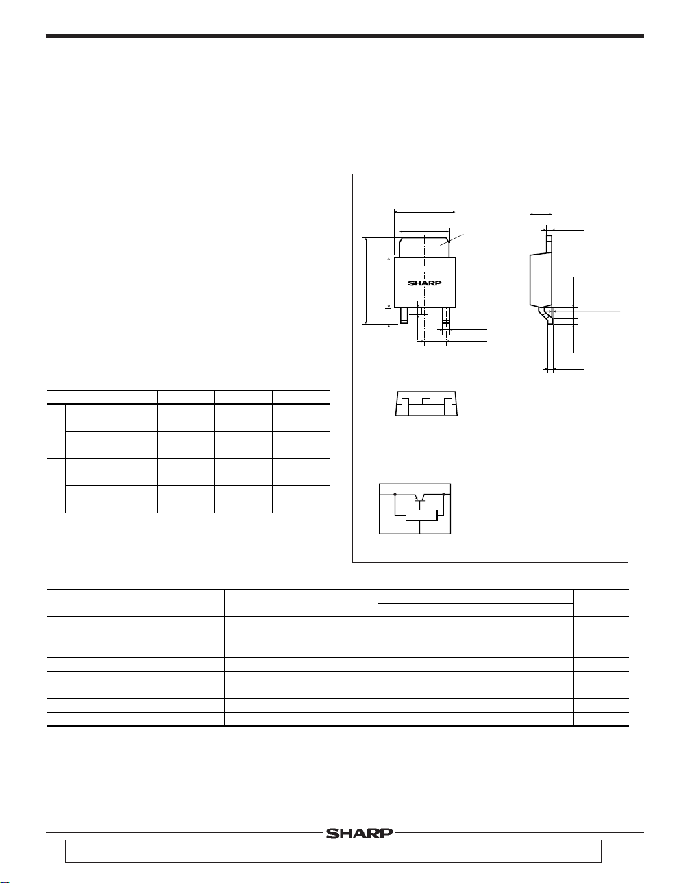
■ Outline Dimensions
6.6MAX
5.2±0.5
05SZ5
9.7MAX
5.5±0.5
0.7MAX
2.5MIN
122
Internal connection diagram
1
Specific IC
3
3
2
+0.2
0.5
-0.1
2-(2.54)
(Unit : mm)
2.3±0.5
(0.5)
(0.9) (1.7)
(0.5)
1 DC input (V
2 DC output (V
3 GND
Heat sink is common to 2 (V
IN
)
O
)
(0to0.25)
O
).
■ Absolute Maximum Ratings
Parameter
Input voltage
Input-output reverse voltage
Output current
Power dissipation
Junction temperature
Operating temperature
Storage temperature
Soldering temperature
*1
All are open except GND and applicable terminals.
*2
With imfinite heat sink.
*
Over heat protection may operate at T
“ In the absence of confirmation by device specification sheets,SHARP takes no responsibility for any defects that may occur in equipment using any SHARP devices
shown in catalogs,data books,etc.Contact SHARP in order to obtain the latest version of the device specification sheets before using any SHARP's device. ”
j
>=125˚C
(Ta=25˚C, XX=05,09,12)
Symbol
V
IN
VO-
I
O
P
D
T
j
T
opr
T
stg
T
sol
i
Conditions
*1
VIN=0V
Refer to Fig. 4
*
For 10s
Rating
PQXXSZ5/51
24
13
*2
0.5
8
150
-
20 to +80
-
40 to +150
260
· Please refer to the chapter“ Handling Precautions ”.
PQXXSZ1/11
1.0
(XX:05,09,12)
Unit
V
V
A
W
˚C
˚C
˚C
˚C
Page 2
Low Power-Loss Voltage Regulators PQ05SZ5/PQ05SZ1 Series
■ Electrical Characteristics
Parameter Symbol Conditions
VO
RegL
R
T
RR
V
VIN=7V
IN=11V
V
IN=14V
V
IN=7V
V
IN=11V
V
IN=14V
V
*4
IO=5mA,
egI
IO=5mA, Tj=0 to 125˚C,
CVO
Refer to Fig. 2
IO=0.5A
*7
i-O
I
O=0A,
I
Iq
*6
*5
O=0.3A
PQ05SZ1/5
PQ09SZ1/5
Output voltage
PQ12SZ1/5
PQ05SZ11/51
PQ09SZ11/51
PQ12SZ11/51
Load regulation
Line regulation
Temperature coefficient of output voltage
Ripple rejection
XXSZ1/11
Dropout voltage
PQ
XXSZ5/51
PQ
Quiescent current
*3
PQxxSZ1/11 Series:Io=0.5A
PQxxSZ5/51 Series:Io=0.3A
*4
PQ05SZ1/11:V
PQ09SZ1/11:VIN=11V, Io=5mA to 1.0A PQ09SZ5/51:VIN=11V, Io=5mA to 0.5A
PQ12SZ1/11:VIN=14V, Io=5mA to 1.0A PQ12SZ5/51:VIN=14V, Io=5mA to 0.5A
*5
PQ05SZ1/11/5/51:V
PQ09SZ1/11/5/51:VIN=10 to 20V
PQ12SZ1/11/5/51:VIN=13 to 23V
*6
PQ05SZ1/11/5/51:V
PQ09SZ1/11/5/51:VIN=11V
PQ12SZ1/11/5/51:VIN=14V
*7
Input voltage shall be the value when output voltage is 95% in comparison with the initial value.
IN=7V, Io=5mA to 1.0A PQ05SZ5/51:VIN=7V, Io=5mA to 0.5A
IN=6 to 16V
IN=7V
Fig.1 Test Circuit
(Tj=25˚C, xx=05,09,12)
UnitMAX.TYP.MIN.
4.75
8.55
*3
11.4
4.88
8.78
11.7
*6
45
5.0
9.0
12.0
5.0
9.0
12.0
-
0.2
-
0.1
-
±0.01
-
0.2
-
4.0
5.25
9.45
12.6
5.12
V
9.22
12.3
2.0
2.5
-
60
-
0.5
10.0
%
%
%/˚C
dB
V
mA
VIN
0.33µF
●2●1
●3
A
Iq
47µF
+
VO
IO
A
V
RL
Fig.2 Test Circuit of Ripple Rejection
●2●1
~
e
i
●3
rms
i/eo
47µF
)
VIN
0.33µF
f=120Hz (sine wave)
i
=0.5V
e
VIN= 7V (PQ05SZ1/11/5/51)
IN
=11V (PQ09SZ1/11/5/51)
V
IN
=14V (PQ12SZ1/11/5/51)
V
O
=0.3A
I
RR=20 log (e
+
IO
+
V
eO
RL
~
Fig.3 Overcurrent Protection
Characteristics(Typical Value)
100
80
PQxxSZ5/51
60
PQxxSZ1/11
40
20
Relative output voltage (%)
0
0
0.3 0.6 0.9 1.2 1.5 1.8 2.1
Output current IO (A)
Page 3
Low Power-Loss Voltage Regulators PQ05SZ5/PQ05SZ1 Series
Fig.4 Power Dissipation vs. Ambient
Temperature
10
(W)
D
5
Power dissipation P
0
-20 0020 40 60 80 100
Ambient temperature Ta (˚C)
Note) Oblique line portion:Overheat
Fig.6
Output Voltage Deviation vs. Junction Temperature
With infinite heat sink
P
D
protection may operate in this area.
(PQ09SZ1/PQ09SZ11/PQ09SZ5/PQ09SZ51)
+100
V
IN=11V
I
O=5mA
Fig.5
Output Voltage Deviation vs. Junction Temperature
(PQ05SZ1/PQ05SZ11/PQ05SZ5/PQ05SZ51)
+50
V
IN=7V
I
O=5mA
0
Output voltage deviation ∆VO (mV)
-50
-25 0
25 50 75 100 125
Junction temperature Tj (˚C)
Fig.7
Output Voltage Deviation vs. Junction Temperature
(PQ12SZ1/PQ12SZ11/PQ12SZ5/PQ12SZ51)
IN=14V
V
+100
I
O=5mA
0
Output voltage deviation ∆VO (mV)
-100
-25 0 25 50 75 100 125
Junction temperature Tj (˚C)
Fig.8 Output Voltage vs. Input Voltage
(PQ05SZ1/PQ05SZ11)
7
Tj=25˚C
6
L
=∞
R
5
(V)
L
=10Ω
R
O
R
L
=5Ω
4
3
2
Output voltage V
1
0
123456789100
Input voltage V
IN
(V)
0
Output voltage deviation ∆VO (mV)
-100
-25 0 25 50 75 100 125
Junction temperature Tj (˚C)
Fig.9 Output Voltage vs. Input Voltage
(PQ05SZ5/PQ05SZ51)
7
6
(V)
5
O
RL=∞
4
3
2
Output voltage V
1
0
123456789100
Input voltage V
R
RL=20Ω
L
=10Ω
IN
Tj=25˚C
(V)
Page 4

Low Power-Loss Voltage Regulators PQ05SZ5/PQ05SZ1 Series
Fig.10 Output Voltage vs. Input Voltage
(PQ09SZ1/PQ09SZ11)
Tj=25˚C
10
(V)
O
RL=∞
RL=18Ω
5
RL=9Ω
Output voltage V
0
0 5 10 15
Input voltage V
IN
(V)
Fig.12 Output Voltage vs. Input Voltage
(PQ12SZ1/PQ12SZ11)
15
Tj=25˚C
RL=∞
(V)
RL=24Ω
O
10
RL=12Ω
Fig.11 Output Voltage vs. Input Voltage
(PQ09SZ5/PQ09SZ51)
Tj=25˚C
Tj=25˚C
L
=
L
=∞
R
R
R
L
=18Ω
L
=18Ω
R
R
R
L
=36Ω
L
=36Ω
(V)
O
10
10
5
5
Output voltage V
0
0
0 5 10 15 20
Input voltage V
IN
(V)
Fig.13 Output Voltage vs. Input Voltage
(PQ12SZ5/PQ12SZ51)
Tj=25˚C
R
L=∞
R
10
L =48Ω
L=24Ω
R
5
Output voltage V
0
0 5 10 15 20
Input voltage V
IN
(V)
Fig.14-a Dropout Voltage vs. Junction
Temperature (PQ05SZ5/51 Series)
0.6
0.5
0.4
0.3
IO=0.5A
0.2
Dropout voltage Vi-O (V)
0.1
-25 0
25 50 75 100 125
Junction temperature Tj (˚C)
IO=0.4A
Io=0.3A
IO=0.2A
IO=0.1A
5
Output voltage VO (V)
0
0 5 10 15 20
Fig.14-b
Dropout Voltage vs. Junction
Temperature (PQ05SZ1/11 Series)
0.6
0.5
(V)
-O
0.4
i
0.3
0.2
Dropout voltage V
0.1
-25 0
Input voltage VIN (V)
O
=1.0A
I
IO=0.75A
IO=0.50A
IO=0.25A
25 50 75 100 125
Junction temperature Tj (˚C)
Page 5

Low Power-Loss Voltage Regulators PQ05SZ5/PQ05SZ1 Series
Fig.15 Circuit Operating Current vs. Input
Voltage (PQ05SZ1/PQ05SZ11)
30
Tj=25˚C
(mA)
BIAS
20
R
L
=5Ω
10
L
=10Ω
R
Circuit operating current I
0
12345678910
Input voltage V
RL=∞
IN
(V)
Fig.17 Circuit Operating Current vs. Input
Voltage (PQ09SZ1/PQ09SZ11)
30
Tj=25˚C
(mA)
BIAS
20
L
=9Ω
10
R
R
L
=18Ω
Fig.16 Circuit Operating Current vs. Input
Voltage (PQ05SZ5/PQ05SZ51)
Tj=25˚C
(mA)
BIAS
20
R
L
=10Ω
L
=20Ω
10
Circuit operating current I
0
0 5 10 15 20
Input voltage V
R
L
=∞
R
IN
(V)
Fig.18 Circuit Operating Current vs. Input
Voltage (PQ09SZ5/PQ09SZ51)
Tj=25˚C
(mA)
BIAS
20
R
L
=18Ω
R
L
10
=36Ω
R
L
=∞
R
L
Circuit operating current I
0
0 5 10 15
Input voltage V
=∞
IN
(V)
Fig.19 Circuit Operating Current vs. Input
Voltage (PQ12SZ1/PQ12SZ11)
30
Tj=25˚C
(mA)
BIAS
20
L
=12Ω
10
Circuit operating current I
0
0 5 10 15 20
Input voltage V
R
R
L
=24Ω
R
L
=∞
IN
(V)
Circuit operating current I
0
0 5 10 15 20
Input voltage V
IN
(V)
Fig.20 Circuit Operating Current vs. Input
Voltage (PQ12SZ5/PQ12SZ51)
Tj=25˚C
(mA)
BIAS
20
R
L
=24Ω
R
L
10
Circuit operating current I
0
0 5 10 15 20
Input voltage V
=48Ω
R
L
=∞
IN
(V)
Page 6

Low Power-Loss Voltage Regulators PQ05SZ5/PQ05SZ1 Series
Fig.21
Quiescent Current vs. Junction Temperature
(PQ05SZ1/PQ05SZ11/PQ09SZ1/PQ09SZ11/PQ12SZ1/
PQ12SZ11)
7
V
IN
=7V (PQ05SZ1/PQ05SZ11)
=11V (PQ09SZ1/PQ09SZ11)
6
=14V (PQ12SZ1/PQ12SZ11)
I
O
=0A
5
(mA)
q
4
3
2
Quiescent current I
1
0
-20 0
25 50 75 100 125
Junction temperature Tj (˚C)
Fig.23
Ripple Rejection vs. Input Ripple Frequency
(PQ05SZ5/PQ05SZ51/PQ09SZ5/PQ09SZ51/PQ12SZ5/
PQ12SZ51)
80
PQ05SZ5/51
70
PQ09SZ5/51
60
50
40
30
20
Ripple rejection RR (dB)
10
0
0.1 0.5 1 5 10 50 100
PQ12SZ5/51
j
=25˚C
T
IN
=7V (PQ05SZ5/51)
V
=11V (PQ09SZ5/51)
=14V (PQ12SZ5/51)
IO=0.3A ei=0.5V
RR=20log(e
i/e0
rms
(sine wave)
)
Input ripple frequency f (kHz)
Fig.25 Ripple Rejection vs. Output Current
(PQ05SZ5/51/ PQ09SZ5/51/ PQ12SZ5/51)
80
60
40
T
VIN=7V (PQ05SZ5/51)
=11V (PQ09SZ5/51)
20
=14V (PQ12SZ5/51)
Ripple rejection RR (dB)
e
f=120Hz
0
PQ05SZ5/51
PQ12SZ5/51
j
=25˚C
i
=0.5V
rms
(sine wave)
Output current IO (A)
PQ09SZ5/51
0.50 1.0
Fig.22
Ripple Rejection vs. Input Ripple Frequency
(PQ05SZ1/PQ05SZ11/PQ09SZ1/PQ09SZ11/PQ12SZ1/
PQ12SZ11)
80
70
PQ05SZ1/11
PQ09SZ1/11
60
50
40
30
20
Ripple rejection RR (dB)
10
0
0.1 0.5 1 5 10 50 100
PQ12SZ1/11
T
j
=25˚C
V
IN
=7V (PQ05SZ1/11)
=11V (PQ09SZ1/11)
=14V (PQ12SZ1/11)
I
O
=0.3A
e
i
=0.5V
rms
RR=20log (e
(sine wave)
i
/e0)
Input ripple frequency f (kHz)
Fig.24 Ripple Rejection vs. Output Current
(PQ05SZ1/11/ PQ09SZ1/11/ PQ12SZ1/11)
80
60
40
T
VIN=7V (PQ05SZ1/11)
=11V (PQ09SZ1/11)
20
=14V (PQ12SZ1/11)
Ripple rejection RR (dB)
e
f=120Hz
0
PQ05SZ1/11
PQ12SZ1/11
j
=25˚C
i
=0.5V
rms
(sine wave)
Output current IO (A)
PQ09SZ1/11
0.50 1.0
Fig.26 Input-Output Reverse Current vs.
Input-Output Reverse Voltage
V
o-i
I
o-i
(OUT)(mA)
i
V
IN
O-
5
PQ05SZ1/PQ05SZ11
PQ05SZ5/PQ05SZ51
0
0
Input-output reverse current I
Input-output reverse voltage I
A
V
O
GND
PQ09SZ1/PQ09SZ11
PQ09SZ5/PQ09SZ51
PQ12SZ1/PQ12SZ11
PQ12SZ5/PQ12SZ51
5 101520
O-i
(V)
Page 7

Low Power-Loss Voltage Regulators PQ05SZ5/PQ05SZ1 Series
Fig.27 Power Dissipation vs. Ambient
Temperature (Typical Value)
4.00
3.00
(W)
D
2.73
Cu area740mm
2.26
2.00
Cu area 180mm
1.48
Cu area 36mm
1.00
0.90
Power dissipation P
0
-20 0
Ambient temperature Ta (˚C)
2
2
2
25 50 75 100 125
Fig.28 Power Dissipation vs. Cu Area
10
Ta=25˚C
7.0
5.0
(W)
3.0
max
D
2.0
1.0
0.7
0.5
Power dissipation P
0.3
10 2 3 5 7 2 3 5 7 1000100
Cu area (mm2)
PWB
PWB
Cu
Material : Glass-cloth epoxy resin
Size : 50X50X1.6mm
Cu thickness : 35µm
3
■ Model Line-ups for Tape-packaged Products
Sleeve-packaged products
Output current
output
0.5A
output
1.0A
Standard type
PQ05SZ5 Series
PQ05SZ1 Series
High-precision output type
PQ05SZ51 Series
PQ05SZ11 Series
Tape-packaged products
Standard type
PQ05SZ5T Series
PQ05SZ1T Series
High-precision output type
PQ05SZ5U Series
PQ05SZ1U Series
 Loading...