

Page 1

DISCRETE SEMICONDUCTORS
DATA SH EET
PN4416; PN4416A
N-channel field-effect transistor
Product specification
File under Discrete Semiconductors, SC07
December 1997
Page 2
Philips Semiconductors Product specification
N-channel field-effect transistor PN4416; PN4416A
FEATURES
• Low noise
• Interchangeability of drain and
source connections
• High gain.
DESCRIPTION
N-channel symmetrical silicon
junction FETs in a SOT54 envelope.
These devices are intended for use in
VHF/UHF amplifiers, oscillators and
mixers.
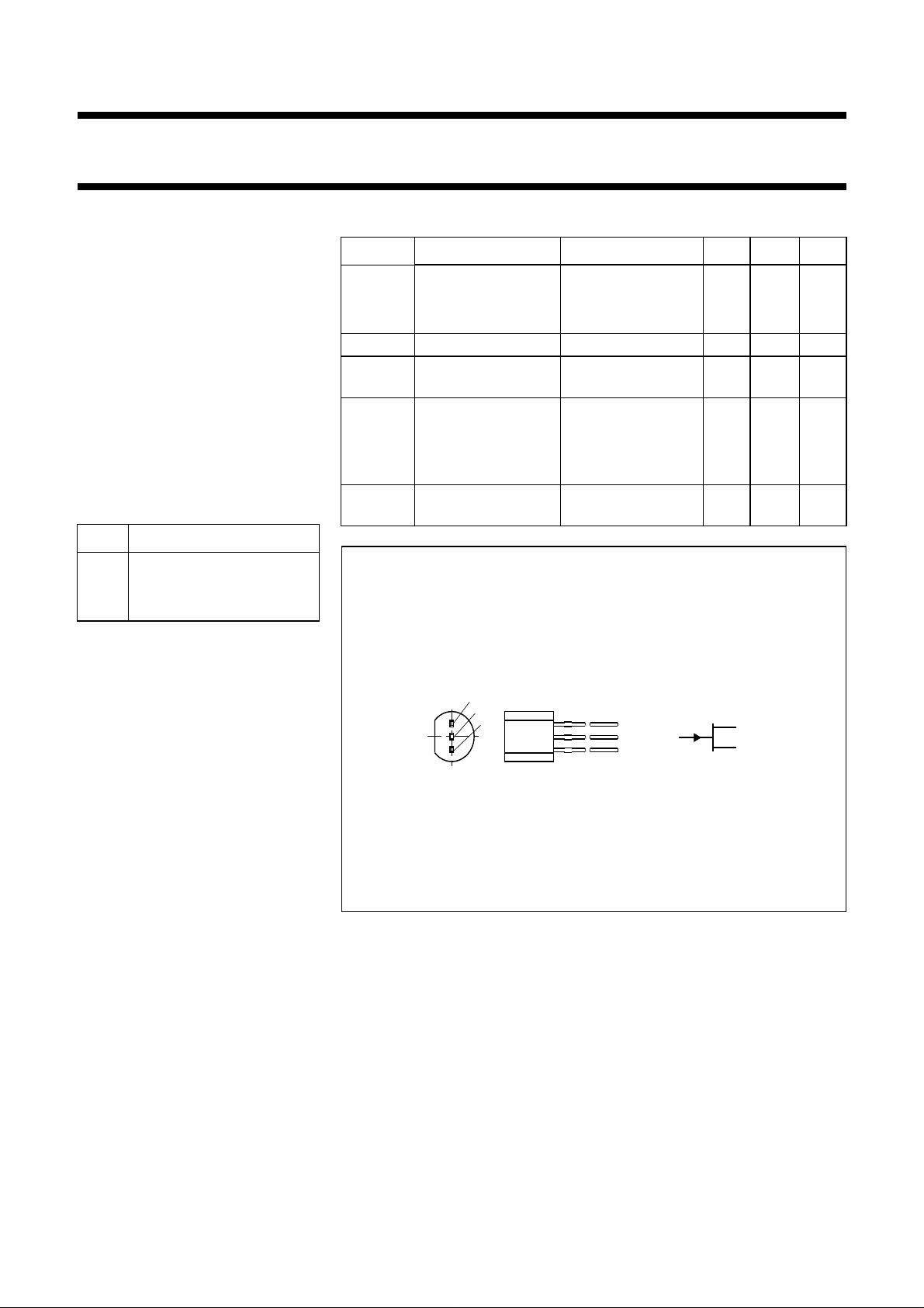
PINNING - SOT54 (TO-92).
PIN DESCRIPTION
1 gate
2 source
3 drain
QUICK REFERENCE DATA
SYMBOL PARAMETER CONDITIONS MIN. MAX. UNIT
V
DS
drain-source voltage
PN4416 − 30 V
PN4416A − 35 V
I
DSS
P
tot
drain current VDS = 15 V; VGS = 0 5 15 mA
total power
up to T
= 25 °C − 400 mW
amb
dissipation
V
GS(off)
gate-source cut-off
voltage
VDS = 15 V;
= 1 nA
I
D
PN4416 −−6V
PN4416A −2.5 −6V
Y
common-source
fs
transfer admittance
VDS = 15 V;
VGS = 0; f = 1 kHz
4.5 7.5 mS
handbook, halfpage
1
2
3
Fig.1 Simplified outline and symbol.
MAM042
g
d
s
December 1997 2
Page 3

Philips Semiconductors Product specification
N-channel field-effect transistor PN4416; PN4416A
LIMITING VALUES
In accordance with the Absolute Maximum Rating System (IEC 134).
SYMBOL PARAMETER CONDITIONS MIN. MAX. UNIT
V
V
V
I
G
P
T
T
DS
GSO
GDO
tot
stg
j
drain-source voltage
PN4416 − 30 V
PN4416A − 35 V
gate-source voltage
PN4416 −−30 V
PN4416A −−35 V
gate-drain voltage
PN4416 −−30 V
PN4416A −−35 V
DC forward gate current − 10 mA
total power dissipation up to T
= 25 °C (note 1) − 400 mW
amb
storage temperature −65 +150 °C
junction temperature − 150 °C
THERMAL RESISTANCE
SYMBOL PARAMETER THERMAL RESISTANCE
R
th j-a
from junction to ambient (note 1) 350 K/W
Note
2
1. Mounted on a printed-circuit board, maximum lead length 4 mm, mounting pad for drain leads 10 mm
.
STATIC CHARACTERISTICS
= 25 °C unless otherwise specified.
T
j
SYMBOL PARAMETER CONDITIONS MIN. MAX. UNIT
V
(BR)GSS
gate-source breakdown voltage VDS = 0; IG = −1 µA
PN4416 −30 − V
PN4416A −35 − V
I
GSS
I
DSS
V
GSS
V
GS(off)
reverse gate leakage current VDS = 0; VGS = −15 V −−1nA
drain current VDS = 15 V; VGS = 0 5 15 mA
gate-source forward voltage VDS = 0; IG = 1 mA − 1V
gate-source cut-off voltage VDS = 15 V; ID = 1 nA
PN4416 −−6V
PN4416A −2.5 −6V
common source transfer admittance VDS = 15 V; VGS = 0 4.5 7.5 mS
Y
fs
common source output admittance VDS = 15 V; VGS = 0
Y
os
PN4416 − 50 µS
PN4416A − 50 µS
December 1997 3
Page 4

Philips Semiconductors Product specification
N-channel field-effect transistor PN4416; PN4416A
DYNAMIC CHARACTERISTICS
T
= 25 °C; VDS = 15 V; VGS = 0.
j
SYMBOL PARAMETER CONDITIONS MIN. TYP. MAX. UNIT
C
is
C
os
C
rs
g
is
g
fs
g
rs
goscommon source output conductance f = 100 MHz −−75 µS
V
n
input capacitance f = 1 MHz −−4pF
output capacitance f = 1 MHz −−2pF
feedback capacitance f = 1 MHz −−0.8 pF
common source input conductance f = 100 MHz −−100 µS
f = 400 MHz −−1mS
common source transfer conductance f = 100 MHz − 5.2 − mS
f = 400 MHz 4 5 − mS
common source feedback conductance f = 100 MHz −−8−µS
f = 400 MHz −−100 −µS
f = 400 MHz −−100 µS
equivalent input noise voltage f = 100 Hz − 5 − nV/√Hz
25
handbook, halfpage
I
DSS
(mA)
20
15
10
5
0
0246
VDS = 15 V; Tj = 25 °C.
Fig.2 Drain current as a function of
gate-source cut-off voltage; typical values.
–V
GS(off)
MRC168
(V)
GS(off)
MRC169
(V)
10
handbook, halfpage
Y
fs
(mS)
8
6
4
2
0
0246
VDS = 15 V; Tj = 25 °C.
–V
Fig.3 Common source transfer admittance as a
function of gate-source cut-off voltage;
typical values.
December 1997 4
Page 5

Philips Semiconductors Product specification
N-channel field-effect transistor PN4416; PN4416A
–V
GS(off)
MRC167
(V)
80
handbook, halfpage
G
os
µ
( S)
60
40
20
0
0123456
VDS = 15 V; Tj = 25 °C.
Fig.4 Common source output conductance as a
function of gate-source cut-off voltage;
typical values.
12
handbook, halfpage
I
D
(mA)
8
4
0
0 4 8 12 16
Tj = 25 °C.
Fig.5 Typical output characteristics.
MRC163
VGS= 0 V
–0.5 V
–1V
VDS(V)
12
handbook, halfpage
I
D
(mA)
8
4
0
–5 –4 –3 –2 –1 0
VDS = 15 V; Tj = 25 °C.
Fig.6 Typical input characteristics.
MRC164
VGS(V)
handbook, halfpage
1
C
rs
(pF)
0.8
0.6
0.4
0.2
0
–10 –8 –6 –4 –2 0
VDS = 15 V; Tj = 25 °C.
Fig.7 Typical feedback capacitance.
MRC158
VGS(V)
December 1997 5
Page 6

Philips Semiconductors Product specification
N-channel field-effect transistor PN4416; PN4416A
3.5
handbook, halfpage
C
is
(pF)
3
2.5
2
1.5
1
0.5
0
–10 –8 –6 –4 –2 0
VDS = 15 V; Tj = 25 °C.
Fig.8 Typical input capacitance.
MRC157
VGS(V)
4
10
handbook, halfpage
–I
G
(pA)
3
10
2
10
10
1
–1
10
–2
10
048121620
ID= 1 mA
MRC165
0.1 mA
I
GSS
VDG(V)
Fig.9 Gate current as a function of drain-gate
voltage, typical values.
500
handbook, halfpage
P
tot
(mW)
400
300
200
100
0
0 50 100 150
T
amb
Fig.10 Power derating curve.
MRC139
o
( C)
100
handbook, halfpage
g , b
isis
(mS)
10
1
0.1
0.01
10 100 1000
VDS = 15 V; VGS = 0; T
amb
b
g
= 25 °C.
MRC160
is
is
f (MHz)
Fig.11 Common source input conductance; typical
values.
December 1997 6
Page 7

Philips Semiconductors Product specification
N-channel field-effect transistor PN4416; PN4416A
100
handbook, halfpage
g , –b
fsfs
(mS)
10
1
0.1
10 100 1000
VDS = 15 V; VGS = 0; T
amb
= 25 °C.
g
fs
–b
fs
f (MHz)
Fig.12 Common source transfer conductance;
typical values.
100
handbook, halfpage
g , b
osos
(mS)
10
b
os
1
0.1
g
os
0.01
10 100 1000
f (MHz)
MRC159
MRC161
100
handbook, halfpage
–g , –b
rs
rs
(mS)
10
–b
rs
1
0.1
0.01
0.001
10 100 1000
VDS = 15 V; VGS = 0; T
amb
= 25 °C.
–g
rs
f (MHz)
Fig.13 Common source feedback conductance;
typical values.
SPICE parameters for PN4416
September 1992; version 1.0.
1VTO =−3.553 V
2 BETA = 792.6 µA/V
3 LAMBDA = 18.46 m/V
4 RD = 7.671 Ω
5 RS = 7.671 Ω
6 IS = 333.4 aA
7 CGSO = 2.920 pF
8 CGDO = 2.261 pF
9 PB = 1.090 V
10 (note 1) FC = 500.0 m
Note
1. Parameter not extracted; default value.
MRC162
2
VDS = 15 V; VGS = 0; T
amb
= 25 °C.
Fig.14 Common source output conductance;
typical values.
December 1997 7
Page 8

Philips Semiconductors Product specification
N-channel field-effect transistor PN4416; PN4416A
PACKAGE OUTLINE
Plastic single-ended leaded (through hole) package; 3 leads SOT54
c
E
d
A L
1
D
2
3
b
1
0 2.5 5 mm
scale
DIMENSIONS (mm are the original dimensions)
UNIT
Note
1. Terminal dimensions within this zone are uncontrolled to allow for flow of plastic and terminal irregularities.
A
5.2
mm
5.0
OUTLINE
VERSION
SOT54 TO-92 SC-43
b
0.48
0.40
b
c
D
d
1
0.66
0.45
0.40
4.8
4.4
0.56
IEC JEDEC EIAJ
E
1.7
4.2
1.4
3.6
REFERENCES
e
2.54
e
1.27
1
L
14.5
12.7
L
1
(1)
L
1
2.5
EUROPEAN
PROJECTION
b
e
1
e
ISSUE DATE
97-02-28
December 1997 8
Page 9

Philips Semiconductors Product specification
N-channel field-effect transistor PN4416; PN4416A
DEFINITIONS
Data sheet status
Objective specification This data sheet contains target or goal specifications for product development.
Preliminary specification This data sheet contains preliminary data; supplementary data may be published later.
Product specification This data sheet contains final product specifications.
Short-form specification The data in this specification is extracted from a full data sheet with the same type
number and title. For detailed information see the relevant data sheet or data handbook.
Limiting values
Limiting values given are in accordance with the Absolute Maximum Rating System (IEC 134). Stress above one or
more of the limiting values may cause permanent damage to the device. These are stress ratings only and operation
of the device at these or at any other conditions above those given in the Characteristics sections of the specification
is not implied. Exposure to limiting values for extended periods may affect device reliability.
Application information
Where application information is given, it is advisory and does not form part of the specification.
LIFE SUPPORT APPLICATIONS
These products are not designed for use in life support appliances, devices, or systems where malfunction of these
products can reasonably be expected to result in personal injury. Philips customers using or selling these products for
use in such applications do so at their own risk and agree to fully indemnify Philips for any damages resulting from such
improper use or sale.
December 1997 9
 Loading...