

Page 1

Released
Data Sheet
PMC-2000164 ISSUE 3 ENHANCED TT1™ SWITCH FABRIC
PMC-Sierra, Inc.
PM9311/2/3/5 ETT1™ CHIP SET
PM9311/2/3/5
Enhanced TT1 Chip Set
Enhanced TT1 Switch Fabric
Datasheet
Issue 3: August 2001
PROPRIETARY AND CONFIDENTIAL TO P MC-SIERRA, INC.,AND FOR ITS CUSTOMERS’ INTERNAL USE
Page 2

Released
Data Sheet
PMC-2000164 ISSUE 3 ENHANCED TT1™ SWITCH FABRIC
PMC-Sierra, Inc.
PM9311/2/3/5 ETT1™ CHIP SET
This document is the proprietaryand confidential information of PMC-Sierra Inc. Access to this information
does not transfer or grant any right or license to use this intellectual property. PMC-Sierra will grant such
rights only under a separate written license agreement.
Any product, process or technology described in this document is subject to intellectual property rights
reserved by PMC-Sierra, Inc.and are not licensed hereunder. Nothing contained herein shall be construed
as conferring by implication, estoppel or otherwise any license or right under any patent or trademark of
PMC-Sierra, Inc.or any third party. Except as expressly provided for herein, nothing contained herein shall
be construed as conferring any license or right under any PMC-Sierra, Inc.copyright.
Each individual document published by PMC-Sierra, Inc. may contain additional or other proprietary
notices and/or copyright information relating to that individual document.
THE DOCUMENT MAYCONTA IN TE CHNICAL INACCURACIES OR TYPOGRAPHICAL ERRORS.
CHANGES ARE REGULARLY MADE TO THE INFORMATION CONTAINED IN THE DOCUMENTS.
CHANGES MAYOR MAY NOT BE INCLUDED IN FUTURE EDITIONS OF THE DOCUMENT.
PMC-SIERRA, INC.OR ITS SUPPLIERS MAY MAKE IMPROVEMENTS AND/OR CHANGES IN THE
PRODUCTS(S), PROCESS(ES), TECHNOLOGY, DESCRIPTION(S), AND/OR PROGRAM(S)
DESCRIBED IN THE DOCUMENT AT ANY TIME.
THE DOCUMENT IS PROVI DED "AS IS" WITHOUT WARRANTY OF ANY KIND, EITHER EXPRESS OR
IMPLIED, INCLUDING BUT NOT LIMITED TO ANY IMPLIED WARRANTY OR MERCHANTABILITY,
FITNESS FOR A PARTICULAR PURPOSE, OR NON-INFRINGEMENT.
ETT1, Enhanced TT1, TT1, and LCS are trademarks of PMC-Sierra, Inc.
© 2000
PMC-Sierra, Inc.
8555 Baxter Place
Burnaby BC Canada V5A 4V7
Phone: (604) 415-6000 FAX: (604) 415-6200
PROPRIETARY AND CONFIDENTIAL TO PMC-SIERRA, INC., AND FOR ITS CUSTOMERS’ INTERNAL USE
Page 3

Released
Data Sheet
PMC-2000164 ISSUE 3 ENHANCED TT1™ SWITCH FABRIC
PMC-Sierra, Inc.
PM9311/2/3/5 ETT1™ CHIP SET
Device Part Numbers
This document contains information on the ETT1TMChip Set,available from PMC-Sierra, Inc. The following
devices comprise the ETT1 Chip Set:
Device Name PMC Part Number
Scheduler PM9311-UC
Crossbar PM9312-UC
Dataslice PM9313-HC
Enhanced PortProcessor PM9315-HC
PROPRIETARY AND CONFIDENTIAL TO PMC-SIERRA, INC., AND FOR ITS CUSTOMERS’ INTERNAL USE
Page 4

Released
Data Sheet
PMC-2000164 ISSUE 3 ENHANCED TT1™ SWITCH FABRIC
PMC-Sierra, Inc.
PM9311/2/3/5 ETT1™ CHIP SET
Revision History
Issue Number Issue Date Details Of Change
1 March 2000 Creation of document
2 July 2000 Added HSTL Power Dissipation values, corrected programming
constraints for EPP, added OOB, JTAG and PLL blocks to device
dataflow diagrams, added heat sink information to Characteristics
section, corrected EPP register section, corrected Frame Format
tables, added correct bit definition for EPP Interrupt register,
corrected diagram in Appendix C, added send and receive
procedure for control packets, added ESOBLCP register
explanation, corrected conditions in Table 57, corrected Scheduler
Refresh Procedure, added new drawing for Crossbar data flow,
corrected token explanation, corrected Figures 36 and 37,
corrected spelling and formatting errors throughout document.
3 August 2001 Removed bit 17 from Scheduler Status Register, updated BP_FIFO
information in Scheduler Control and Reset Register, corrected
bottom view drawings for Scheduler and Crossbar, corrected signal
description section in Scheduler and Crossbar for power pins,
corrected tper3, and tpl3 in AC Electrical, added memory address
information in EPP registers, corrected mechanical drawings,
updated state diagram in Scheduler, added information about
Scheduler PLL timing, updated initialization sequence for all chips,
corrected DatasliceSignal Descriptionfor ibpen0, added bit 14(13th
and 14th Dataslice enable) to EPP Control register, updated TDM
constraints, added Output TDM Queue Overflow to the EPP’s
Interrupt register, updated EPP Output Backpressure /
Unbackpressure Threshold register, updated LCS2 link
synchronization in appendix, modified EPP Egress Control Packet
Data Format table, Modified ETT1 usage of LCS2 protocol section
PROPRIETARY AND CONFIDENTIAL TO PMC-SIERRA, INC., AND FOR ITS CUSTOMERS’ INTERNAL USE
Page 5

Released
Data Sheet
PMC-2000164 ISSUE 3 ENHANCED TT1™ SWITCH FABRIC
PMC-Sierra, Inc.
PM9311/2/3/5 ETT1™ CHIP SET
1 Functional Description . . . . . . . . . . . . . . . . . . . . . . . . . . . . . . . . . . . . . . . . . . . . 15
1.1 Overview.........................................................15
1.1.1 ETT1SwitchCoreFeatures...................................................15
1.1.2 TheSwitchCoreModel ......................................................16
1.1.3 TheLCSProtocol...........................................................17
1.1.4 TheOOB(Out-Of-Band)Bus..................................................18
1.2 Architecture and Features. . ......................................... 18
1.2.1 ETT1SwitchCore ..........................................................18
1.2.2 BasicCellFlow.............................................................19
1.2.3 PrioritizedBest-effortService..................................................21
1.2.4 End-to-EndFlowControl .....................................................22
1.2.5 TDMService...............................................................22
1.2.6 SubportMode(2.5Gbit/sLinecards)............................................23
1.2.7 LCSControlPackets ........................................................24
1.2.8 Redundancy...............................................................25
1.2.9 SystemConfigurationOptions.................................................28
1.3 Prioritized Best-Effort Q ueue Model .................................. 30
1.3.1 UnicastTraffic(OC-192)......................................................31
1.3.2 MulticastTraffic(OC-192) ....................................................31
1.3.3 UnicastTraffic(SubportMode).................................................33
1.3.4 MulticastTraffic(subportmode)................................................46
1.3.5 CombinationsofOC-192candQuadOC-48cLinecards.............................49
1.3.6 Summary.................................................................50
1.3.7 TheLCSProtocol...........................................................51
1.4 Explicit Backpressure From oEPP to iEPP ............................. 52
1.4.1 FlowControlCrossbarSynchronization..........................................54
1.5 TDMService...................................................... 54
1.5.1 TDMQueues..............................................................54
1.5.2 TDMReservationTables.....................................................55
1.5.3 TDMFrameTiming..........................................................59
1.5.4 TDMSynchronization........................................................59
1.5.5 ConfiguringtheTDMService..................................................62
1.5.6 ChangingtheSourceoftheSuggestedSync......................................63
1.6 ETT1 Usage of the LCS Protocol ..................................... 64
1.6.1 LCSProtocolPrepend.......................................................64
1.6.2 UseofLabelandTypeFields..................................................67
1.6.3 ControlPackets ............................................................69
1.6.4 UseofCRCFields..........................................................73
1.6.5 LCSPHYLayer ............................................................75
1.7 TheOut-of-Band(OOB)BusInterface................................. 77
1.7.1 TheOOBBus..............................................................78
PROPRIETARY AND CONFIDENTIAL TO PMC-SIERRA, INC., AND FOR ITS CUSTOMERS’ INTERNAL USE i
Page 6

Released
Data Sheet
PMC-2000164 ISSUE 3 ENHANCED TT1™ SWITCH FABRIC
PMC-Sierra, Inc.
PM9311/2/3/5 ETT1™ CHIP SET
1.8 Initialization Procedure .............................................84
1.8.1 InitialPower-on:............................................................85
1.8.2 PortBoardbeingadded:......................................................87
1.8.3 SchedulerBoardbeingadded:.................................................89
1.8.4 CrossbarBoardbeingadded:..................................................90
1.9 Fault Tolerance. ................................................... 91
1.9.1 FaultToleranceModel.......................................................91
1.9.2 Soft/Transient Errors . . . . . . . . . . . . . . . . . . . . . . . . . . . . . . . . . . . . . . . . . . . . . . . . . . . . . . . . 93
1.9.3 FlowControlRefreshProcedure ...............................................97
1.9.4 SchedulerRefreshProcedure .................................................98
1.9.5 RefreshSchedulersAfterModifyingRegisters.....................................99
1.9.6 HardErrors................................................................99
1.10 ETT1 Signals and Interconnections .................................. 102
1.10.1 LVCMOS(CandO)........................................................102
1.10.2 HSTL(H) ................................................................102
1.10.3 AIBLinks(A)..............................................................103
1.10.4 LiveInsertion .............................................................104
1.11 System Latencies................................................. 104
1.11.1 LCSRequesttoGrantMinimumLatency........................................105
1.11.2 LCSGranttoLinecardCellLatency............................................105
1.11.3 CelllatencyThroughanEmptySystem.........................................106
1.11.4 LCSHoleRequesttoHoleGrantLatency.......................................107
1.12 ETT1Diagnostics.................................................108
1.12.1 DeviceTests..............................................................108
1.12.2 AIBLinkTests ............................................................109
1.12.3 LinecardtoETT1LinkDiagnostics.............................................109
1.12.4 ETT1InternalDatapathTests ................................................113
2 Dataslice.......................................................115
2.1 Dataslice Blocks.................................................. 115
2.1.1 OOBInterfaceandControl/StatusRegisters.....................................117
2.1.2 DatasliceCellFlow.........................................................117
2.2 8B/10BInterface..................................................118
2.3 DatasliceRegisters...............................................119
2.3.1 DatasliceSummary ........................................................119
2.3.2 DatasliceRegisterDescriptions...............................................121
2.4 Dataslice Signal Descriptions.......................................136
ii PROPRIETARY AND CONFIDENTIAL TO PMC-SIERRA, INC., AND FOR ITS CUSTOMERS’ INTERNAL USE
Page 7

Released
Data Sheet
PMC-2000164 ISSUE 3 ENHANCED TT1™ SWITCH FABRIC
PMC-Sierra, Inc.
PM9311/2/3/5 ETT1™ CHIP SET
2.5 Pinout and Package Information ....................................142
2.5.1 PinoutTables.............................................................142
2.5.2 PackageDimensions.......................................................147
2.5.3 PartNumber..............................................................149
3 EnhancedPortProcessor.........................................151
3.1 EPP Data Flows and Blocks ........................................153
3.1.1 EPPDataFlows...........................................................154
3.1.2 LCSGrantManager........................................................156
3.1.3 SchedulerRequestModulator................................................158
3.1.4 InputQueueManager.......................................................159
3.1.5 OutputQueueManager.....................................................160
3.1.6 OutputScheduler..........................................................161
3.1.7 OOBInterfaceandControl/StatusRegisters.....................................161
3.2 Input Dataslice Queue Memory Allocation w ith EPP . . .................. 162
3.3 Output Dataslice Queue Memory Allocation with EPP. .................. 162
3.4 Enhanced Port Processor Registers ................................. 165
3.4.1 EnhancedPortProcessorSummary ...........................................165
3.4.2 EnhancedPortProcessorRegisterDescriptions..................................169
3.5 Enhanced Port processor Signal Descriptions......................... 209
3.6 Pinout and Package Information ....................................214
3.6.1 PinoutTables.............................................................214
3.6.2 PackageDimensions.......................................................221
3.6.3 PartNumber..............................................................223
4 Crossbar.......................................................225
4.1 Crossbar Blocks.................................................. 225
4.1.1 OOBInterfaceandControl/StatusRegisters.....................................227
4.2 Modes Of Operation...............................................227
4.3 OOB Access . . . .................................................. 227
4.4 Crossbar Registers ............................................... 228
4.4.1 Summary................................................................228
4.4.2 CrossbarRegisterDescriptions...............................................229
4.5 Crossbar Signal Descriptions.......................................237
PROPRIETARY AND CONFIDENTIAL TO PMC-SIERRA, INC., AND FOR ITS CUSTOMERS’ INTERNAL USE iii
Page 8

Released
Data Sheet
PMC-2000164 ISSUE 3 ENHANCED TT1™ SWITCH FABRIC
PMC-Sierra, Inc.
PM9311/2/3/5 ETT1™ CHIP SET
4.6 Pinout and Package Information ....................................240
4.6.1 PinoutTables.............................................................240
4.6.2 PackageDimensions.......................................................249
4.6.3 PartNumber..............................................................251
5 Scheduler......................................................253
5.1 BlockStructure ..................................................253
5.1.1 PortBlock................................................................253
5.1.2 ArbiterBlock..............................................................253
5.1.3 OOBInterfaceandControl/StatusRegisters.....................................254
5.1.4 TDMService..............................................................254
5.2 PortState.......................................................256
5.3 Fault Tolerance. .................................................. 257
5.4 Scheduler Registers ..............................................259
5.4.1 Summary................................................................259
5.4.2 SchedulerRegisterDescriptions ..............................................261
5.4.3 InputQueueMemory(IQM)..................................................275
5.5 Scheduler Signal Descriptions ...................................... 276
5.6 Pinout and Package Information ....................................279
5.6.1 PinoutTables.............................................................279
5.6.2 PackageDimensions.......................................................288
5.6.3 PartNumber..............................................................290
6 Characteristics..................................................293
6.1 Signal Associations............................................... 293
6.2 Absolute Maximum Ratings ........................................297
6.3 Recommended Operating Conditions . . . ............................. 299
6.4 DCElectricalCharacteristics.......................................302
6.5 ACElectricalCharacteristics.......................................305
6.6 TimingDiagrams.................................................308
AppendixA GeneralPacket/FrameFormats...........................317
iv PROPRIETARYAND CONFIDENTIAL TO PMC-SIERRA, INC., AND FOR ITS CUSTOMERS’ INTERNAL USE
Page 9

Released
Data Sheet
PMC-2000164 ISSUE 3 ENHANCED TT1™ SWITCH FABRIC
PMC-Sierra, Inc.
PM9311/2/3/5 ETT1™ CHIP SET
A.1 Frame Formats - Dataslice To and From Enhanced Port Processor........ 317
A.2 FrameFormats-DatasliceToandFromCrossbar...................... 318
A.3 Frame Formats - Enhanced Port Processor To and From Scheduler....... 319
Appendix B Common Pinout Configuration . . . . . . . . . . . . . . . . . . . . . . . . . . . 323
B.1 JTAGInterface................................................... 323
B.2 Reserved Manufacturing Test Pins ..................................323
B.3 Power Supply Connections. ........................................ 324
B.4 Example Power Up Sequence....................................... 325
AppendixC InterfacingDetailsforETT1..............................327
C.1 Compensating for Round Trip Delay Between Linecard and ETT1(LCS) .... 327
C.1.1 PreventingUnderflowoftheVOQ .............................................327
C.2 The8b/10bInterfacetotheDataslice................................. 328
C.2.1 Link.....................................................................329
C.2.2 Channel.................................................................333
C.3 Managing Cell Rates (Setting the Idle Count Register) .................. 335
C.4 AvoidingDelaysDuetoIdleCells ................................... 336
PROPRIETARY AND CONFIDENTIAL TO PMC-SIERRA, INC., AND FOR ITS CUSTOMERS’ INTERNAL USE v
Page 10

Released
Data Sheet
PMC-2000164 ISSUE 3 ENHANCED TT1™ SWITCH FABRIC
PMC-Sierra, Inc.
PM9311/2/3/5 ETT1™ CHIP SET
vi PROPRIETARYAND CONFIDENTIAL TO PMC-SIERRA, INC., AND FOR ITS CUSTOMERS’ INTERNAL USE
Page 11

Released
Data Sheet
PMC-2000164 ISSUE 3 ENHANCED TT1™ SWITCH FABRIC
PMC-Sierra, Inc.
PM9311/2/3/5 ETT1™ CHIP SET
Figure 1. The Basic Components of a Switch Built Around the ETT1 Chip Set.. . . ...............16
Figure2. ETT1SwitchCoreLogicalInterconnects........................................18
Figure3. TwoPortConfigurationofaETT1Switch.......................................20
Figure4. QueueingandFlowControl..................................................22
Figure5. TheTDMFrameConcept ...................................................23
Figure 6. Fully Redundant Core . . . . . . . . . . ............................................26
Figure 7. Simple Redundant Scheduler Configuration . . . . . . . . . ............................27
Figure8. LCSCellSlicedAcrossDataslicesandCrossbars ................................29
Figure9. TheUnicastIngressQueueingModelforOnePort................................31
Figure10. IngressandEgressQueueforMulticastTraffic...................................33
Figure11. AnETT1PortOperatinginSubportModewithFourOC-48cLinecards................34
Figure12. TheInputRequestCounters.................................................35
Figure13. FullSetofCountersforaSinglePriority........................................36
Figure14. AllRequestCountersforaSingleOutputShareaSingleQueue.....................38
Figure15. SequenceofEventsattheInputSide..........................................40
Figure16. VirtualInputQueues.......................................................43
Figure17. TheFourPriorities.........................................................45
Figure18. SchedulerRequests/GrantsareMultiplexedataPortLevel.........................46
Figure19. EachiEPPhasaSingleVirtualOutputQueueforMulticastCells.....................47
Figure20. MulticastCellProcessing....................................................47
Figure21. EITIBMstructure ..........................................................48
Figure22. OITIBMstructure..........................................................49
Figure23. SchedulerPriorities........................................................50
Figure24. ETT1PortIngressQueues ..................................................51
Figure 25. A Separate Crossbar is Used to Convey Backpressure Information to the iEPPs. . . . . . . . . 53
Figure 26. The Queueing Structure. . . . . . . . . ............................................55
Figure27. IngressPortLogic .........................................................57
Figure28. TheoEPPMustTreattheTransferredTDMCellasaMulticastCell...................58
Figure29. SingleTDMTable .........................................................59
Figure30. TDMSynchronization.......................................................60
Figure31. SignalFlow...............................................................62
Figure 32. One Implementation: The OOB Bus Consists of Both Local and Global Buses . . . . . . . . . . 77
Figure 33. The Global Device Select Defines the Board Number and the Device on Each Board . . . . . 80
Figure34. WriteCycle-NoWait.......................................................82
Figure35. WriteCycle-OneWait......................................................82
Figure36. ReadCycle-OneWait .....................................................83
Figure37. ReadCycle-TwoWaits.....................................................83
Figure38. InterruptsareActiveHighandSynchronous.....................................84
Figure 39. Redundant Connections . . . . . . . . ............................................92
Figure40. SimpleNon-RedundantCrossbarConfiguration..................................93
Figure41. SimpleNon-RedundantSchedulerConfiguration.................................95
PROPRIETARY AND CONFIDENTIAL TO PMC-SIERRA, INC., AND FOR ITS CUSTOMERS’ INTERNAL USE vii
Page 12

Released
Data Sheet
PMC-2000164 ISSUE 3 ENHANCED TT1™ SWITCH FABRIC
PMC-Sierra, Inc.
PM9311/2/3/5 ETT1™ CHIP SET
Figure 42. Simple Redundant Crossbar Configuration . . . . . . . . . . ............................95
Figure 43. Simple Redundant Scheduler Configuration . . . . . . . . . ............................96
Figure 44. ETT1 Signals and Interconnects . . ...........................................102
Figure45. AIBLinks...............................................................103
Figure46. AIBControl/StatusSignals..................................................104
Figure47. RequesttoGrantlatency...................................................105
Figure48. ETT1EventLatencies.....................................................106
Figure49. CellLatency.............................................................107
Figure50. IllustratingtheFlowofCellsfromtheLinecardCPUtotheETT1CPU................110
Figure51. LoopbackPath...........................................................111
Figure52. ControlPacketExchangeBetweenLinecardCPUandETT1CPU...................112
Figure53. TestingtheETT1InternalDatapaths..........................................113
Figure54. DatasliceDataFlow.......................................................116
Figure55. SlicingofaDataCellintoLogicalDataslices....................................117
Figure56. DatasliceCBGAPackageDimensions-TopandSideViews.......................147
Figure57. DatasliceCBGAPackageDimensions-BottomView.............................148
Figure58. AnETT1PortOperatinginSub-portModewithFourOC-48cLinecards..............152
Figure59. FunctionalDiagramofLCSEnhancedPortProcessor............................153
Figure 60. Enhanced Port Processor CBGA Package Dimensions - Top and Side Views. . . . . . . . . . 221
Figure 61. Enhanced Port Processor (EPP) CBGA Package Dimensions - Bottom View . . . . . . . . . . 222
Figure62. TheBasicDataflowThroughtheCrossbar.....................................226
Figure63. CrossbarCCGAPackageDimensions-TopandSideViews.......................249
Figure64. CrossbarCCGApackageDimensions-BottomView.............................250
Figure65. SchedulerBlockDiagram...................................................255
Figure66. PortStateMachine........................................................256
Figure67. SchedulerCCGApackageDimensions-TopandSideViews......................288
Figure68. SchedulerCCGApackageDimensions-BottomView............................289
Figure 69. Setup and Hold for 3.3V-tolerant 2.5V CMOS and 2.5V CMOS (OOB Interface) . . . . . . . . 308
Figure 70. Rise and Fall Times for 3.3V-tolerant 2.5V CMOS and 2.5V CMOS (OOB Interface). . . . . 309
Figure 71. OOB Test Loading ........................................................309
Figure 72. Setup and Hold for 3.3V-tolerant 2.5V CMOS and 2.5V CMOS (JTAG Interface). . . . . . . . 310
Figure 73. Rise and Fall Times for 3.3V-tolerant 2.5V CMOS and 2.5V CMOS (JTAG Interface) . . . . 310
Figure74. JTAGTestLoading.......................................................310
Figure 75. Setup and Hold for 3.3V-tolerant 2.5V CMOS and 2.5V CMOS (Serdes Interface) . . . . . . 311
Figure 76. Rise and Fall Times for 3.3V-tolerant 2.5V CMOS and 2.5V CMOS (Serdes Interface) . . . 311
Figure77. SerdesTestLoading......................................................311
Figure78. SetupandHoldfor200MbpsHSTL(EPP/DSInterface)...........................312
Figure79. RiseandFallTimesfor200MbpsHSTL(EPP/DSInterface).......................312
Figure80. Class1HSTLTestLoading.................................................313
Figure81. SetupandHoldfor800MbpsSTI(AIBInterfaces)...............................314
Figure82. RiseandFallTimesfor800MbpsSTI(AIBInterfaces))...........................314
viii PROPRIETARY AND CONFIDENTIAL TO PMC-SIERRA, INC., AND FOR ITS CUSTOMERS’ INTERNAL USE
Page 13

Released
Data Sheet
PMC-2000164 ISSUE 3 ENHANCED TT1™ SWITCH FABRIC
PMC-Sierra, Inc.
PM9311/2/3/5 ETT1™ CHIP SET
Figure83. AIBTestLoading.........................................................315
Figure84. SetupandHoldfor2.5V200MbpsPECL(CLK&SOCSignals)....................316
Figure85. ClockPeriodandDutyCyclefor2.5V200MbpsPECL(CLKSignal).................316
Figure86. ExampleNoiseIsolationCircuit..............................................325
Figure87. ExampleVoltageDivider...................................................325
Figure88. VoltageRamp-up.........................................................326
Figure89. TheTimeAvailabletotheLinecard...........................................328
Figure90. CellsareStripedAcrossthe12PhysicalLinks..................................329
Figure91. The10-bitDataPaths .....................................................330
Figure 92. Initial Sequence Expected at Port Card . . . . . . . . . . . . . ...........................331
Figure93. CellsMayBeSkewedBetweenDataslices.....................................335
Figure94. TheIdleCounterCanDelayanOutboundCell..................................337
Figure95. TheIdleCounterCanDelayanOutboundCell..................................337
Figure96. One-deepQueueforOutboundRequests......................................339
PROPRIETARY AND CONFIDENTIAL TO PMC-SIERRA, INC., AND FOR ITS CUSTOMERS’ INTERNAL USE ix
Page 14

Released
Data Sheet
PMC-2000164 ISSUE 3 ENHANCED TT1™ SWITCH FABRIC
PMC-Sierra, Inc.
PM9311/2/3/5 ETT1™ CHIP SET
x PROPRIETARY AND CONFIDENTIAL TO PMC-SIERRA, INC., AND FOR ITS CUSTOMERS’ INTERNAL USE
Page 15

Released
Data Sheet
PMC-2000164 ISSUE 3 ENHANCED TT1™ SWITCH FABRIC
PMC-Sierra, Inc.
PM9311/2/3/5 ETT1™ CHIP SET
Table1. CrossbarConfigurations ....................................................30
Table2. TDMReservationTable ....................................................55
Table3. LCSFormatfromLinecardtoSwitch ..........................................65
Table4. DefinitionsofLCSFieldsfromLinecardtoSwitch ................................65
Table5. LCSFormatfromSwitchtoLinecard ..........................................66
Table6. DefinitionsofLCSFieldsfromSwitchtoLinecard ................................66
Table7. Encodingof4-bitTypeFields ................................................67
Table8. UsageoftheIngressRequestLabel_1.........................................67
Table9. UsageoftheEgressGrantLabel_1 ...........................................68
Table10. UsageoftheEgressPayloadLabel_2 .........................................68
Table11. LCSControlPacketFormat .................................................70
Table12. TDMControlPacketFormat .................................................71
Table13. RequestCountControlPacketFormat .........................................71
Table14. Start/StopControlPacketFormat .............................................72
Table15. Fiber1.5Gbit/sperChannelInterfaceConfigurations .............................76
Table 16. Mapping Segments to 1.5 Gbit/s Channels . . . . . . . . . . ............................76
Table17. OOBControlBusSignals ...................................................78
Table18. MulticastGroupSelects ....................................................79
Table19. UnicastGroupSelects .....................................................81
Table20. Refresh-sensitiveRegistersintheScheduler ...................................99
Table21. DatasliceRegisterSummary ...............................................119
Table22. DatasliceSignalDescriptions ...............................................136
Table23. DataslicePinout(leftside) .................................................142
Table24. DataslicePinout(rightside) ................................................143
Table18. DatasliceAlphaPinList ...................................................144
Table19. DatasliceCBGAMechanicalSpecifications ....................................148
Table 20. Linecard Request Count Maximum Values . . . . . . . . . . ...........................157
Table21. InputDatasliceQueueMemoryAllocation .....................................162
Table22. OutputDatasliceQueueMemoryAllocation ....................................163
Table23. EPPEgressControlPacketDataFormatandDatasliceOOBAddressing ............164
Table24. EnhancedPortProcessorRegisterSummary ..................................165
Table25. EnhancedPortProcessorSignalDescriptions .................................209
Table26. EnhancedPortProcessorPinout(leftside) ....................................214
Table27. EnhancedPortProcessorPinout(center)......................................215
Table28. EnhancedPortProcessorPinout(rightside) ...................................216
Table35. EnhancedPortProcessorAlphaPinList ......................................217
Table 36. Enhanced Port Processor CBGA Mechanical Specifications . . . . . . . . . ..............222
Table37. CrossbarRegisterSummary................................................228
Table38. CrossbarSignalDescriptions ..............................................237
Table39. CrossbarPinout(leftside)..................................................240
Table40. CrossbarPinout (center) ..................................................241
PROPRIETARY AND CONFIDENTIAL TO PMC-SIERRA, INC., AND FOR ITS CUSTOMERS’ INTERNAL USE xi
Page 16

Released
Data Sheet
PMC-2000164 ISSUE 3 ENHANCED TT1™ SWITCH FABRIC
PMC-Sierra, Inc.
PM9311/2/3/5 ETT1™ CHIP SET
Table41. CrossbarPinout(rightside) ................................................242
Table33. CrossbarAlphaPinList....................................................243
Table34. CrossbarCCGAMechanicalSpecifications ....................................250
Table35. Non-TDMTraffic .........................................................257
Table36. SchedulerRegisterSummary ...............................................259
Table37. SchedulerSignalDescriptions ..............................................276
Table38. SchedulerPinout(leftside).................................................279
Table39. SchedulerPinout(center) ..................................................280
Table40. SchedulerPinout(rightside)................................................281
Table41. SchedulerAlphaPinList...................................................282
Table42. SchedulerCCGAMechanicalSpecifications ...................................289
Table43. SignalAssociations ......................................................293
Table44. AbsoluteMaximumRatings ................................................297
Table 45. Absolute Maximum Ratings for 3.3V-tolerant 2.5V CMOS (OOB & Serdes Interface) . . . . 297
Table46. AbsoluteMaximumRatingsfor2.5VCMOS(JTAGInterface) ......................297
Table47. AbsoluteMaximumRatingsfor200MbpsHSTL(EPP/DSInterface).................297
Table48. AbsoluteMaximumRatingsfor800MbpsSTI(AIBInterface) ......................298
Table 49. Absolute Maximum Ratings for 2.5V 200 Mbps PECL (CLK and SOC Signals) . . . . . . . . . 298
Table50. RecommendedOperatingConditions.........................................299
Table51. AdditionalPowerDesignRequirements .......................................301
Table 52. DC Electrical Characteristics for 3.3V-tolerant 2.5V CMOS (OOB Interface) . . . . . . . . . . 302
Table53. DCElectricalCharacteristicsfor2.5VCMOS(JTAGInterface) .....................302
Table54. DCElectricalCharacteristicsfor3.3V-tolerant2.5VCMOS(Serdes) ................303
Table55. DCElectricalCharacteristicsfor200MbpsHSTL(EPP/DSInterface) ...............303
Table56. DCElectricalCharacteristicsfor800MbpsSTI(AIBInterfaces) ....................304
Table 57. DC Electrical Characteristics for 2.5V 200 Mbps PECL (CLK and SOC Signals) . . . . . . . 304
Table 58. AC Electrical Characteristics for 3.3V-tolerant 2.5V CMOS (OOB Interface) . . . . . . . . . . . 305
Table59. ACElectricalCharacteristicsfor2.5VCMOS(JTAGInterface) .....................305
Table 60. AC Electrical Characteristics for 3.3V-tolerant 2.5V CMOS (Serdes Interface) . . . . . . . . . 306
Table61. ReferenceClockfor200MbpsHSTL(EPP/DSInterface) .........................306
Table62. ACElectricalCharacteristicsfor800MbpsSTI(AIBInterface) ....................307
Table63. ACElectricalCharacteristicsfor2.5V200MbpsPECL(CLKSignals) ................307
Table64. JitterandStaticPhaseOffsetforPLL.........................................308
Table65. Request/DatafromiDSFrameFormat ........................................317
Table66. DatafromoDSFrameFormat ..............................................317
Table67. Grant/DatatoiDSFrameFormat ............................................317
Table68. ControltoxDSLinkFormat ................................................318
Table69. DataslicetoCrossbarFrameFormat .........................................318
Table70. CrossbartoDatasliceFrameFormat .........................................319
Table71. SchedulertoEPPFrameFormat ............................................319
Table72. EPPtoSchedulerFrameFormat ............................................321
xii PROPRIETARY ANDCONFIDENTIAL TO PMC-SIERRA,INC., ANDFOR ITS CUSTOMERS’ INTERNAL USE
Page 17

Released
Data Sheet
PMC-2000164 ISSUE 3 ENHANCED TT1™ SWITCH FABRIC
PMC-Sierra, Inc.
PM9311/2/3/5 ETT1™ CHIP SET
Table73. Suggested8b/10bDecodeMapWithintheDataslice.............................331
Table74. DatasliceEgressTruthTable ...............................................331
Table75. ProgrammedTokenDelayvs.Inter-linkSkew ..................................334
PROPRIETARY AND CONFIDENTIAL TO PMC-SIERRA, INC., AND FOR ITS CUSTOMERS’ INTERNAL USE xiii
Page 18

Released
Data Sheet
PMC-2000164 ISSUE 3 ENHANCED TT1™ SWITCH FABRIC
PMC-Sierra, Inc.
PM9311/2/3/5 ETT1™ CHIP SET
xiv PROPRIETARY AND CONFIDENTIAL TO PMC-SIERRA, INC., AND FOR ITS CUSTOMERS’ INTERNAL USE
Page 19

Released
Data Sheet
PMC-2000164 ISSUE 3 ENHANCED TT1™ SWITCH FABRIC
PMC-Sierra, Inc.
PM9311/2/3/5 ETT1™ CHIP SET
1 Functional Description
1.1 OVERVIEW
The ETT1TMChip Set provides a crossbar-based switch core which is capable of switching cells between
32 ports with each port operating at data rates up to 10 Gbit/s. This section describes the main features of
the switch core and how cells flow through a complete system that is based on the ETT1 Chip Set.
This document often refers to port rates of OC-192c or OC-48c. The ETT1 Chip Set itself operates at a
fixed cell rate of 25M cells per second per port and thus is unaware of the actual data rate of the attached
link. So a switchmight be 32 port sof OC-192c, or it could be 32 ports of 10 Gbit/sEthernet; itis the internal
cell rate that is determined by the ETT1 Chip Set, not the link technology.
1.1.1 E TT1 Switch Core Features
The ETT1 switch core provides the following features:
• 320 Gbit/s aggregate bandwidth- up to 32 ports of 10 Gbit/s bandwidth each
• Each port can be configured as 4 x OC-48c or 1 x OC-192c
• Both port configurations support four priorities of best-ef fort traffic for unicast and multicast data
traffic
• TDM support for guaranteed bandwidth and zero delay variation with 10 Mbit/s channel resolution
•LCS
TM
protocol supports a physical separation of switch core and linecards up to 200 feet (70 m)
• Virtual output queues to eliminate head-of-line blocking on unicast cells
• Internal speedup to provide near-output-queued performance
• Cells are transferred using a credit mechanism to avoid cell losses due to buffer overrun
• In-band management and control via Control Packets
• Out-of-band management and control via a dedicated CPU interface
• Optional redundancy of all shared components for fault tolerance
• Efficient support for multicast with cell replication performed within the switch core
PROPRIETARY AND CONFIDENTIAL TO PMC-SIERRA, INC., AND FOR ITS CUSTOMERS’ INTERNAL USE 15
Page 20
Released
Data Sheet
PMC-2000164 ISSUE 3 ENHANCED TT1™ SWITCH FABRIC
PMC-Sierra, Inc.
PM9311/2/3/5 ETT1™ CHIP SET
1.1.2 The Switch Core Model
The ETT1Chip Set is designed to provide a switch core, not a complete packet switch system.A complete
switch consists of one or more switch cores, together with a number of linecards. Each linecard connects
to one port in the core. The linecard includes a physical interface (fiber, co-axial cable) to a transmission
system suchas SONET/SDH or Ethernet. The linecardanalyzes incoming cells or packets and determines
the appropriate egress port and priority. The linecard contains any cell/packet queues that are needed to
allow for transient congestion through the switch.
The ETT1 switch core operates on fixed sizecells. If the linecard transmissionsystem uses variablelength
packets, or cells of a size different from those used in the core, then the linecard is responsible for
performing any segmentation and reassembly that is needed. Figure 1 illustrates this generic
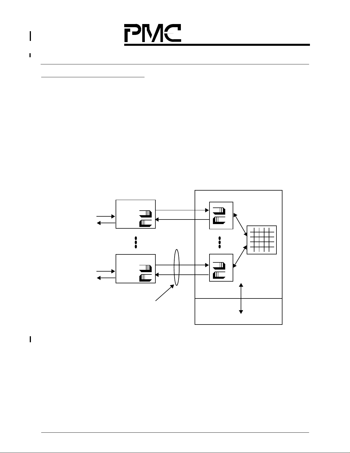
configuration.
Figure 1. The Basic Components of a Switch Built Around the ETT1 Chip Set.
ETT1 Switch Core
port 0
Linecard 0
SONET/SDH
Ethernet....
Linecard 31
SONET/SDH
Ethernet....
port 0
LCS Protocol
ETT1 Chip Set
OOB Bus
CPU
The ETT1 Chip Set has been designed to allow for up to 200 feet (70 meters) of physical separation
between the ETT1 core and the linecard. The LCS
TM
(Linecard to Switch) protocol is used between the
ETT1 core and the linecard to ensure lossless transfer of cells between the two entities. However, while
the LCS protocol must be implemented,the physical separation is not mandatory; the linecard could reside
on the same physical board as the ETT1 port devices.
The switch core has two main interfaces. One is the interface between the linecard and the core port,
described in the LCS Protocol section.
16 PROPRIETARYAND CONFIDENTIAL TO PMC-SIERRA, INC., AND FOR ITS CUSTOMERS’ INTERNAL USE
Page 21

Released
Data Sheet
PMC-2000164 ISSUE 3 ENHANCED TT1™ SWITCH FABRIC
PMC-Sierra, Inc.
PM9311/2/3/5 ETT1™ CHIP SET
The secondinterface is between the ETT1 devices and the local CPU. TheETT1 ChipSet requires a local
CPU for configuration,diagnostics and maintenance purposes. A singleCPU can control a completeETT1
core via a common Out-Of-Band (OOB) bus. All of the ETT1 devices have an interface to the OOB bus.
The OOB bus is described in Section 1.1.4 “The OOB (Out-Of-Band) Bus” on page 18.
1.1.3 The LCS Protocol
The Linecard-to-Switch (LCSTM) protocol provides a simple, clearly defined interface between the linecard
and the core. In this section we introduce LCS. There are two aspects to LCS:
• a per-queue, credit-based flow control protocol
• a physical interface
The LCS protocol provides per-queue, credit-based flow control from the ETT1 core to the linecard, which
ensures that queues are not overrun.The ETT1core has shallow (64 cells)queues in both the ingressand
egress directions. These queues compensate for the latency between the linecard and the core. One way
to think of these queues is simply as extensions of the queues within the linecards. The queues
themselves are described further in Section 1.3 “Prioritized Best-Effort Queue Model” on page 30.
The LCS protocol is asymmetrical; it uses different flow control mechanisms for the ingress and egress
flows. For the ingress flow LCS uses credits to manage the flow of cells between the linecards and the
ETT1 core. The core provides the linecard with a certain number of creditsfor each ingress queue in the
core. These credits correspond to the number of cell requests that the linecard cansend to the core. For
each cell request that is forwardedto a given queuein the core the linecardmust decrementthe number of
credits for that queue. The core sends a grant (which is also a new credit) to the linecard whenever the
core is ready to accept a cell in responseto the cell request. At some later time, which is dependent on the
complete traffic load, the cell will be forwarded through the ETT1 core to the egress port. In the egress
direction a linecard can send hole requests, requesting that the ETT1 core does not forward a cell for one
celltime. The linecard can issue a hole request for each of the four besteffort unicastor multicast priorities.
If the linecard continually issued hole requestsat all four priorities then the ETT1 core would not forward
any best effort traffic to the linecard.
The LCS protocol information is contained within an eight byte header that is added to every cell.
The physical interface that has been implemented in the ETT1 Chip Set is based on a faster version of the
Gigabit EthernetSerdes interface,enabling theuse of off-the-shelf parts for the physical link. This interface
provides a
1.5 Gbit/sserial link that uses 8b/10b encoded data. Twelve of these links are combined to provide a single
LCS link operating at 18Gbaud, providing an effective databandwidth that is in excessof an OC-192clink.
NOTE: The LCS protocol is defined in the “LCS Protocol Specification -- Protocol Version 2”,
available from PMC-Sierra,Inc. This version of LCS supersedes LCS Version 1. Version 2
is first supported in the TT1 Chip Set with the Enhanced Port Processor device (also
referred to as the ETT1 Chip Set) and will be supported in future PMC-Sierra products.
The ETT1 implementation of the LCS protocol is described further in Section 1.6 “ETT1
Usage of the LCS Protocol” on page 64.
PROPRIETARY AND CONFIDENTIAL TO PMC-SIERRA, INC., AND FOR ITS CUSTOMERS’ INTERNAL USE 17
Page 22
Released
Data Sheet
PMC-2000164 ISSUE 3 ENHANCED TT1™ SWITCH FABRIC
PMC-Sierra, Inc.
PM9311/2/3/5 ETT1™ CHIP SET
1.1.4 The OOB (Out-Of-Band) Bus
The ETT1 Chip Set requires a local CPU to perform initialization and configuration after the Chip Set is
reset or if the core configuration is changed - perhaps new ports are added or removed, for example. The
OOB bus provides a simple mechanism whereby a local CPU can configure each device.
Logically, the OOB bus provides a 32 bit address/data bus with read/write, valid and ready signals. The
purpose of the OOB bus is for maintenance and diagnostics; the CPU is not involved in any per-cell
operations.
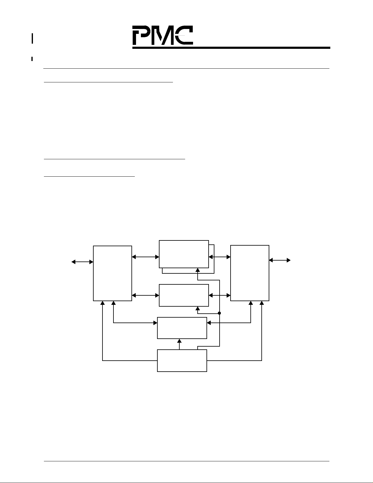
1.2 ARCHITECTURE AND FEATURES
1.2.1 ETT1 Switch Core
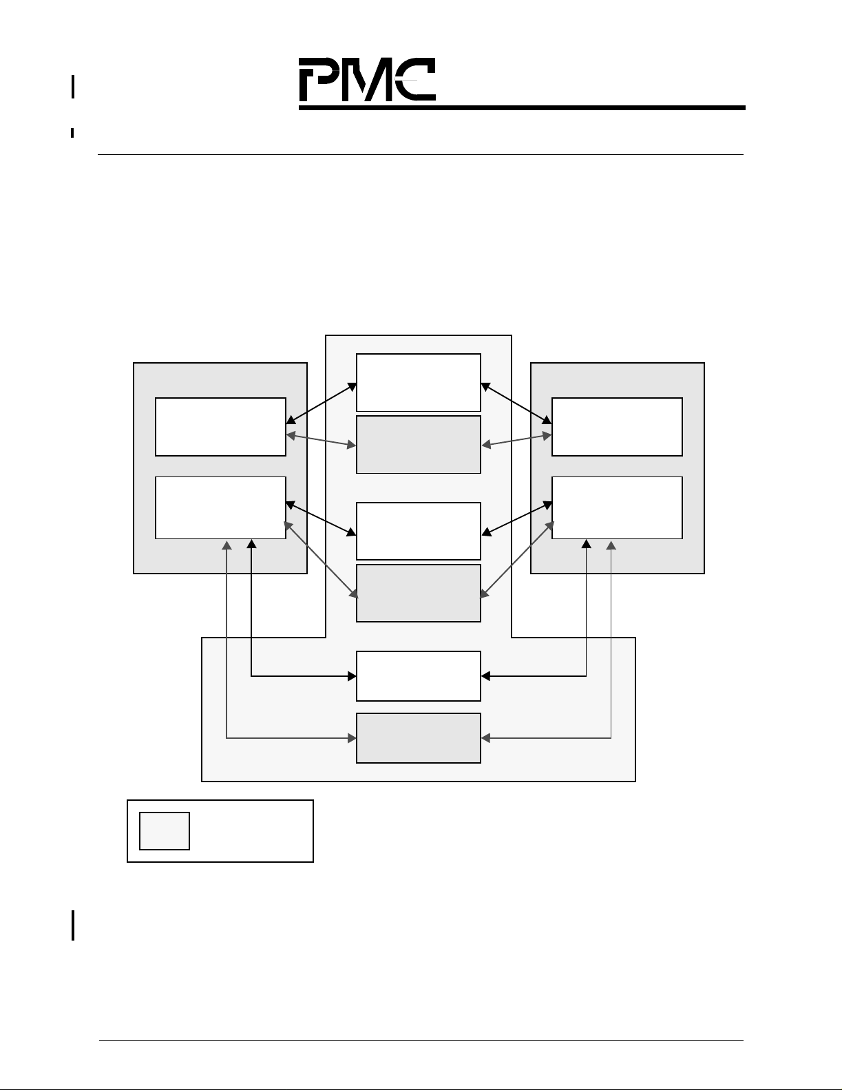
An ETT1 switch core consists of four types of entities: Port, Crossbar, Scheduler, and CPU/Clock. There
may be one or more instances of each entity within a switch. For example, each entity might be
implemented as a separate PCB, with each PCB interconnected via a single midplane PCB. Figure 2
illustrates the logical relationship between these entities.
Linecard
Figure 2. ETT1 Switch Core Logical Interconnec ts
Crossbar
Port
Flow Control
Crossbar
Scheduler
CPU/clock
Linecard
Port
18 PROPRIETARYAND CONFIDENTIAL TO PMC-SIERRA, INC., AND FOR ITS CUSTOMERS’ INTERNAL USE
Page 23

Released
Data Sheet
PMC-2000164 ISSUE 3 ENHANCED TT1™ SWITCH FABRIC
PMC-Sierra, Inc.
PM9311/2/3/5 ETT1™ CHIP SET
Each ETT1 port is attached to one or more linecards. The port contains the shallow cell queues and
implements the LCS protocol. The port and Scheduler exchange information about cells that are waiting to
be forwarded through the Crossbar core.
The Scheduler maintains local information on the number of cells that are waiting in all of the ingress and
egress queues. It arbitrates amongst all cells in the ingress queues, and instructs all of the ports as to
which cell they can forward through the Crossbar at each cell time.
Two Crossbars are used. The first, referred to as simply ‘the Crossbar’, interconnects all of the ports with
all of the other ports, enabling cells to be forwardedfrom the ingress port queues to theegressport queues
(in a different port). The Crossbaris reconfigured at every celltime to provide any non-blocking one-to-one
or one-to-many mapping from input ports to output ports. Each Crossbar port receives its configuration
information from its attached port; the Crossbars do not communicate directly with the Scheduler. The
second Crossbar is the flow-control Crossbar. It passes output queue occupancy information from every
egress port to every ingress port. The ingress ports use this information to determine when requests
should and should not be made to the Scheduler.
The CPU/clock provides clocks and cell boundary information to every ETT1 device. It also has a local
CPU which can read and write state information in every ETT1 device via the OOB bus. The CPU/clock
entity is a necessary element of the ETT1 switch core, but does not contain any of the ETT1 devices.
1.2.2 Basic Cell Flow
The ETT1 Chip Set consists of four devices. Their names (abbreviations) are:
•Dataslice(DS)
• Enhanced Port Processor (EPP)
• Scheduler (Sched)
• Crossbar (Xbar)
This section describes how cells flow through these four devices.
PROPRIETARY AND CONFIDENTIAL TO PMC-SIERRA, INC., AND FOR ITS CUSTOMERS’ INTERNAL USE 19
Page 24
Released
Data Sheet
PMC-2000164 ISSUE 3 ENHANCED TT1™ SWITCH FABRIC
Figure 3. Two P ort Conf igu ration of a ETT1 Switch
PMC-Sierra, Inc.
PM9311/2/3/5 ETT1™ CHIP SET
1,3
2
1,3
Input Data Slice
2,3
5
5
7
Input EPP
Crossbar
Flow Control
Crossbar
6
5
7
Output Data Slice
6
5,7
Output EPP
7
44
Scheduler
data cell flow
control flow
3
6,7
Figure 3 shows a two-port configuration of a ETT1 switch. Only the ingress queues of the left hand port
and theegress queues of the right hand port are shown. The port has one EPP and eithersix or seven DS
devices. The DS contains the cell queue memory and also has the Serdes interface to the linecard. A
single cell is “sliced” across all of the Dataslice devices, each of which can manage two slices. The EPP is
the port controller, and determines where cells should be stored in the DS memories. Multiple Crossbar
devices make up a full Crossbar. A single Scheduler device can arbitrate for the entire core.
A cell traverses the switch core in the following sequence of events:
1. A cell request arrives at the ingress port, and is passed to the EPP. The EPP adds the request to
any other outstanding cell requests for the same queue.
2. At some later time, the EPP issues a grant/credit to the source linecard, requesting an actual cell
for a specific queue. The linecard must respond with the cell within a short period of time.
3. The cell arrives at the ingress port and the LCS header is passed to the EPP. The EPP
determines the destination queue from the LCS header, and then tells the Dataslices where to
store the cell (each Dataslice stores part of the cell). The EPP also informs the Scheduler that a
new cell has arrived and so the Scheduler should add it to the list of cells waiting to be forwarded
through the Crossbar. The EPP modifies the LCS label by replacing the destination port with the
source port, so the egress port and linecard can see which port sent the cell.
4. The Scheduler arbitrates among all queuedcells and sends a granttothose ports that can forward
a cell. The Scheduler also sends a routing tag to each of the destination (egress) ports; this tag
20 PROPRIETARYAND CONFIDENTIAL TO PMC-SIERRA, INC., AND FOR ITS CUSTOMERS’ INTERNAL USE
Page 25

Released
Data Sheet
PMC-2000164 ISSUE 3 ENHANCED TT1™ SWITCH FABRIC
PMC-Sierra, Inc.
PM9311/2/3/5 ETT1™ CHIP SET
tells the ports which of the many source ports will be sending it a cell.
5. The source EPP sends a read command to the Dataslices, which then reads the cell from the
appropriate queue and sends it to the Crossbar. At the same time, the destination ports send the
routing tag information to the Crossbar. This routing tag information is used to configure the
internal connections within the Crossbar for the duration of one cell time. The cell then flows
through the Crossbar from the source port to the destination port.
6. The cell arrives at the destination port, and the EPP receives the LCS header of the cell. It uses
this information to decide in which egress queue the cell should be stored. If this was a multicast
cell which caused the egress multicast to reach its occupancy limit, then the EPP would send a
congestion notification to the Scheduler.
7. At some later time, the EPP decides to forward the cell to the linecard. The EPP sends a read
command to the Dataslices which read the cell from memory and forward the cell out to the
linecard. The egress EPP also sends flow control to the ingress EPP, informing it that there now
exists free space in one or more of the egress EPP’s output queues. Also, if the transmitted cell
was a multicast cell then this may cause the egress queue to go from full to not full, in which case
the EPP notifies the Scheduler that it (the EPP) can once again accept multicast cells.
The above description does not account for all of the interactions that can take place between ETT1
devices, but it describes the most frequent events. In general, users do not need to be aware of the
detailed interactions, however knowledge of the main information flows will assist in gaining an
understanding of some of the more complicated sections.
1.2.3 Prioritized Best-effort Service
An ETT1 switch core provides two types of service. The first is a prioritized,best-effort service. The second
provides guaranteed bandwidth and is described later.
The best-effort service is very simple. Linecards forward best-effort cells to the ETT1 core where they will
be queued. The Scheduler arbitrates among the various cells; the arbitration algorithm has the dual goals
of maximizing throughput while providing fair access to all ports. If more than one cell is destined for the
same egress port then the Scheduler will grant one of the cells and the others will remain in their ingress
queues awaitinganother round of arbitration. The serviceis best-effort in that the Scheduler tries its best to
satisfy all queued cells, but in the case of contention then some cells will be delayed.
The Scheduler support s four levels of strict priority for best effort traffic. Level 0 cells have the highest
priority, and level 3 cells have the lowest priority. A level 0 cell destined for a given port will always be
granted before a cell of a different priority level, in the same ingress port, that is destined for the same
egress port.
A ‘flow’ is a sequence of cells from the same ingress port to the same egress port(s) at a given priority.
Best-effort flows are either unicast flows (cells in the flow go to only one egress port), or multicast flows (in
whichcasecellscangotomany,evenall,oftheegressports).
PROPRIETARY AND CONFIDENTIAL TO PMC-SIERRA, INC., AND FOR ITS CUSTOMERS’ INTERNAL USE 21
Page 26
Released
Data Sheet
PMC-2000164 ISSUE 3 ENHANCED TT1™ SWITCH FABRIC
PMC-Sierra, Inc.
PM9311/2/3/5 ETT1™ CHIP SET
1.2.4 End-to-End Flow Control
The full queueing and flow control model is shown in Figure 4.
NOTE: Creditsor backpressure are used at every transfer point to ensure that cells cannot be lost
due to lack of buffer space.
Figure 4. Queueing and Flow Control
ETT1 core
r
a
Linecard
Ingress queues
ETT1 port
Ingress
queues
b
s
s
o
r
C
1
T
T
E
ETT1 port
Egress
queues
Linecard
Egress queues
LCS credits
cell flow
backpressure/credits
hole requestsETT1 backpressure
1.2.5 TDM Service
The ETT1 TDM service provides guaranteed bandwidth and zero cell delay variation. These properties,
which are not available from the best-effort service, mean that the TDM service might be used to provide
an ATM CBR service, for example. The ETT1 core provides the TDM service at the same time as the best
effort service, and TDM cells integrate smoothly with the flow of best-effort traffic. In effect, the TDM cells
appear to the Scheduler to be cells of the highest precedence, even greater than level zero best-effort
multicast traffic.
The TDM service operates by enabling a ETT1 port (and linecard) to reserve the crossbar fabric at some
specified cell time in the future. The Scheduler is notified of this reservation and will not schedule any
best-effort cells from the ingress port or to the egress port during that one cell time. Each port can make
separate reservations according to whether it will send and/or receive a cell at each cell time.
Several egress ports may receive the same cell from a given ingress port; therefore, the TDM service is
inherently a multicast service.
In order to provide a guaranteed bandwidth over a long period of time, an ingress port will want to repeat
the reservations on a regular basis. To support this the ETT1 core uses an internal construct called a TDM
22 PROPRIETARYAND CONFIDENTIAL TO PMC-SIERRA, INC., AND FOR ITS CUSTOMERS’ INTERNAL USE
Page 27
Released
Data Sheet
PMC-2000164 ISSUE 3 ENHANCED TT1™ SWITCH FABRIC
PMC-Sierra, Inc.
PM9311/2/3/5 ETT1™ CHIP SET
Frame. A TDM Frame is simplya sequence of ingressand egressreservations. The length (number of cell
times) of a TDM Frame is configurable up to a maximum of 1024 cells. The TDM Frame repeat s after a
certain fixed time. All ports are synchronized to the start of the TDM Frame, and operate
cell-synchronouslywith respectto each other. Thus, atany cell time, everyETT1 port knows whether ithas
made a reservation to send or receive a TDM cell. See the application note “LCS-2 TDM Service in the
ETT1 and TTX Switch Core”, available from PMC-Sierra, Inc.
Figure 5 illustrates the idea of a TDM Frame. The TDM Frame has N slots(N is 1024 or less) where each
slot is one 40ns cell time. The TDM Frame is repeated continuously, but adjacent TDM Frames are
separated by a guard band of at least 144 cells.
Figure 5. The TDM Fr ame Concept
40ns
1
One TDM Frame
N
Guard band
All of the ETT1 ports must be synchronized with respect to the start of the TDM Frame. This
synchronization information is distributed via the Scheduler. The Scheduler can generate the
synchronization pulses itself, or it can receive “Suggested Sync” pulses from a ETT1 port which can in turn
receive synchronization signals from a linecard. The linecards do not need to be exactly synchronized to
either the ETT1 core or the other linecards. The LCSprotocol willcompensate forthe asynchrony between
the linecard and the ETT1 core.
1.2.6 S ubport Mode (2.5 Gbit/s Linecards)
An ETT1 switch core can have up to 32 ports. Each port supports a linecard bandwidth in excess of
10 Gbit/s.Thisbandwidth mightbe used by a single linecard (for example, OC-192c), or the ETT1port can
be configured to share this bandwidth among up to four ports, each of 2.5 Gbit/s. This latter mode,
specifically four 2.5 Gbit/s linecards, is referred to as subport mode, or sometimes as quad OC-48c mode.
A single ETT1 switch can have some ports in ‘normal’ mode, and some in subport mode; there is no
restriction. The four levels of prioritized best-effort traffic are available in all configurations. However, there
are some important differences between the two modes. One difference is that the LCS header must now
identify the subport associated with each cell. Two bits in the LCS label fields are used for this purpose, as
described below.
A second difference is that the EPP must carefully manage the output rate of each subport, so as not to
overflow the buffers at the destination linecard, and this is also described below.
PROPRIETARY AND CONFIDENTIAL TO PMC-SIERRA, INC., AND FOR ITS CUSTOMERS’ INTERNAL USE 23
Page 28

Released
Data Sheet
PMC-2000164 ISSUE 3 ENHANCED TT1™ SWITCH FABRIC
PMC-Sierra, Inc.
PM9311/2/3/5 ETT1™ CHIP SET
A thirddifference is thatthe EPP must maintainseparate LCS request counters for each of the subports. It
must also maintain separate egress queues. So the number of queues can increase four-fold in order to
preserve the independence of each subport. Section 1.3 “Prioritized Best-EffortQueue Model” on page 30
describes the various queuing models in great detail.
1.2.6.1
Identifying th e Source Subport
The EPP manages a single physical stream of cells at 25M cells/second. In subport mode the EPP must
look at each incoming cell and determine which subport has sent the cell. The LCS label field is used to
achieve this. Two bitswithin the label(referred toin the LCS Specification as MUX bits) are used to denote
the source subport, numbered 0 through 3. The MUX bits must be inserted in the LCS label before the cell
arrives at the EPP. The MUX bits might be inserted at the source linecards themselves. Alternatively, they
might be inserted by a four-to-one multiplexer device placed between the subport linecards and the EPP.
In this latter case, the multiplexer device might not be able to re-calculate the LCS CRC. For maximum
flexibility, the EPP can be configured to calculate the LCS CRC either with or without the MUX bits.
1.2.6.2
Egress Cell Rate
Within the EPP is an Output Scheduler process which is different from, and should not be confused with,
the ETT1 Scheduler device. At every OC-192 cell time, the Output Scheduler looks at the egress queues
and decides which cell should be forwarded to the attached egress linecard(s). In subport mode, the
Output Scheduler will constrain the egress cell rate so as not to overflow any of the 2.5 Gbit/s links. It does
this by operating in a strict round-robin mode, so that at any OC-192 cell time it will only try to send a cell
for one of the subports. The four 2.5 Gbit/s subports are labeled as 0 through 3 ; at some cell time the
Output Scheduler will only try to send a cell from the egress queues associated with subport 0. In the next
time, it will only consider cells destined for subport 1, etc. If, at any cell time, there are nocells to be sent to
the selected subport, then an Idle (empty) cell is sent. For example, if subports 0 and 3 are connected to
linecards but subports 2 and 4 are disconnected, then the Output Scheduler will send a cell to 0, then an
empty cell, then a cell to 3, then an empty cell, and then repeat the sequence. The effective cell rate
transmitted to each subport will not exceed 6.25 M cells per second.
1.2.7 LCS Control Packets
The LCS protocol provides in-band control packets. These packets (cells) are distinct from normal cell
traffic in that they do not pass through the fabric to an egress linecard, but are intended to cause some
effect within the switch.
There are two classes of Control Packets. The first class, referred to as CPU Control Packets, are
exchanged between the linecard and the ETT1 CPU (via the EPP and Dataslices). The intention is that
CPU Control Packets form the basic mechanism through which the linecard CPU and ETT1 CPU can
exchange information. This simple mechanism is subject to cell loss, and so should be supplemented by
some form of reliable transport protocol that would operate within the ETT1 CPU and the linecards.
The second class, referred to as LCS Control Packets, are used to manage the link between the linecard
and the ETT1 port. These LCS Control Packets can be used to start and stop the flow of cells on the link,
24 PROPRIETARYAND CONFIDENTIAL TO PMC-SIERRA, INC., AND FOR ITS CUSTOMERS’ INTERNAL USE
Page 29

Released
Data Sheet
PMC-2000164 ISSUE 3 ENHANCED TT1™ SWITCH FABRIC
PMC-Sierra, Inc.
PM9311/2/3/5 ETT1™ CHIP SET
to provide TDM synchronizationevent information,and can recover from any grant/credit information that
is lost if cells are corrupted in transmission.
1.2.7.1
Sending a Control Packet f rom the OOB to the Linecard
Before sendinga CPU (OOB to linecard) control packet,the OOB must first write the controlpacketheader
and payload data intothe appropriatelocations in the Dataslice. (See Section3.3 “OutputDataslice Queue
Memory Allocation with EPP”, Table 23, on page 164.) The header for customer-specific CPU control
packets should be written into the Dataslices as shown, but the payload data is completely up to the
customer.
To send the CPU control packet which has been written into Dataslice queue memory, the OOB writes the
ESOBLCP register with the control packet type select in bits [5:4] (see the bit-breakout), and a linecard
fanout in bits [3:0]. If the port is connected to 4 subport linecards, then bits [3:0] are a subport-bitmap. If
the port is connected to one OC-192c linecard, then bit 0 must be set when the OOB wishes to send a CP.
When the CP has been sent to the linecard(s) indicated in bits [3:0], bits [3:0] will read back as 0. Since
control packets have higher priority than any other traffic type, they will be sent immediately, unless the
EPPisprogrammedtosendonlyidlecells.
1.2.7.2
Sending a Control Packet F rom the Linecard to the OOB
The linecard sends control packets to OOB using the regular LCS request/grant/cell mechanism. A CPU
(linecard to OOB) control packet must have the CPU bit set in its request label (See Section 1.1.3 “The
LCS Protocol” on page 17.) When the EPPreceives the cellpayload for a CPU control packet, it stores the
cell in the Dataslices’ Input Queue memories and raises the “Received LC2OOB/CPU Control Packet from
Linecard...” interrupt. (In OC-192c mode, it will always be Linecard 0.)
The input queue for CPU control packets from each linecard is only 8 cells deep, so as soon as the OOB
sees a “Received LC2OOB...” interrupt, it should read the appropriate “Subport* to OOB FIFO Status”
register (0x80..0x8c). Bit [3:0] of that register will tell how many control packet cells are currently in the
input queue; bits 6:4 will tell the offset of the head the 8-cell CPU CP input queue. That queue offset
should be used to form addresses for the Dataslices’ Input Queue memories. See Section 3.2 “Input
Dataslice Queue Memory Allocation with EPP” on page 162, for Dataslice Input Queue memory
addressing. Then the OOB should read those addresses to obtain the CPU CP payload data. When the
OOB has read the CPU CP payload data, it should write the appropriate “Linecard * to OOB FIFO Status”
register (any value). A write to that register, regardless of the write data, will cause the head of the queue
to be dequeued, freeing up that space in the CPU CP input queue.
See Section 1.6.3 “Control Packets” on page 69 for more details.
1.2.8 Redundancy
An ETT1 core can be configured with certain redundant (duplicated) elements. A fully redundant core is
capable of sustaining single errors within any shared device without losing or re-ordering any cells. This
section describes the main aspects of a redundant core. A complete switch may have two ETT1 cores,
PROPRIETARY AND CONFIDENTIAL TO PMC-SIERRA, INC., AND FOR ITS CUSTOMERS’ INTERNAL USE 25
Page 30
Released
Data Sheet
PMC-2000164 ISSUE 3 ENHANCED TT1™ SWITCH FABRIC
PMC-Sierra, Inc.
PM9311/2/3/5 ETT1™ CHIP SET
with linecards dual-homed to both cores, and while this is a valid configuration the ETT1 core does not
provide any specific support for such a configuration.
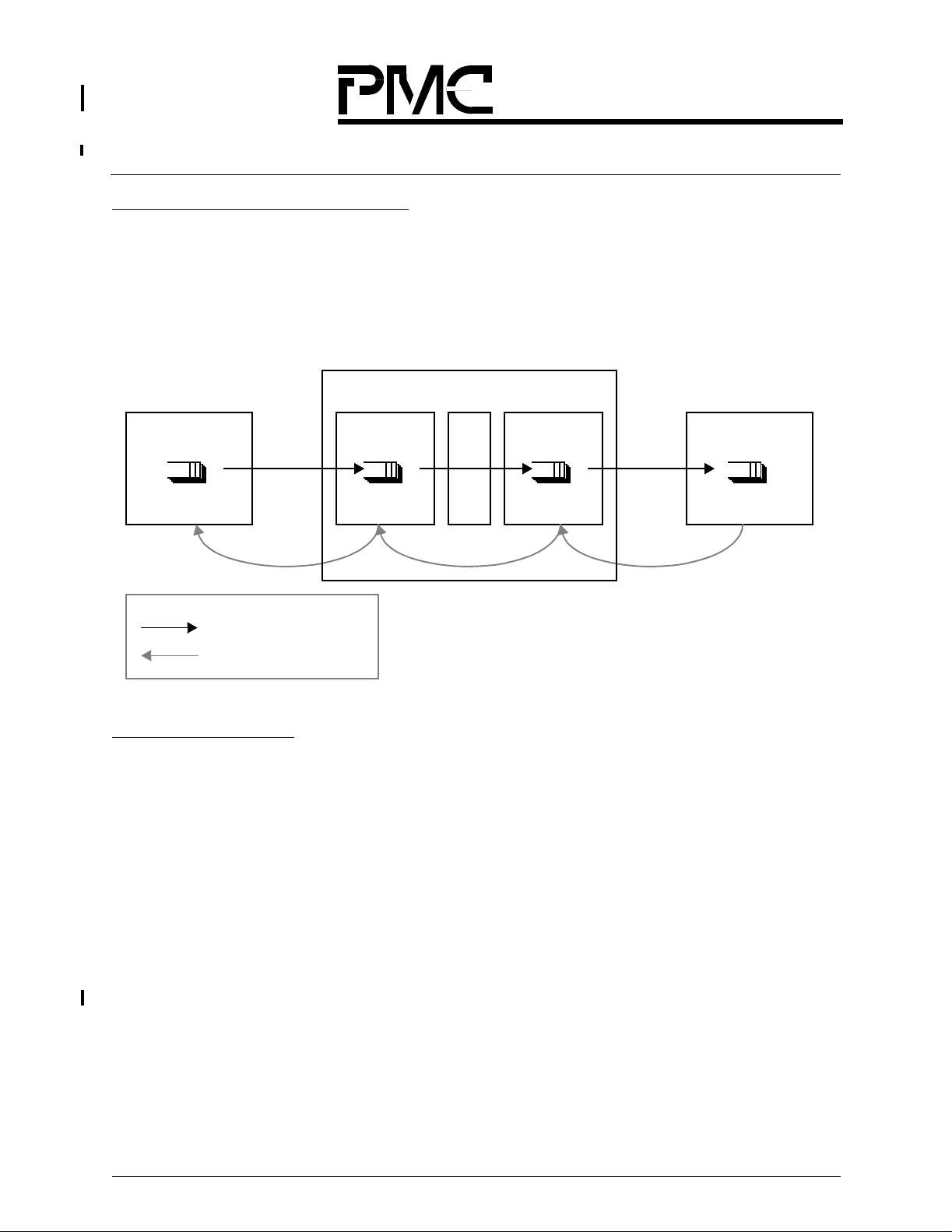
Figure 6 shows a fully redundant core. The Crossbars and Scheduler are fully replicated, as are the links
connecting those devices. The port devices (EPP and Dataslices) are not replicated. It is important to
understand that if an EPP or Dataslice fails (or incurs a transient internal error), then data may be lost, but
only within that port.
Figure 6. Fully R edu ndan t Core
Crossbar 0
Port
Dataslice
EPP
Dataslice
Crossbar 1
EPP
Flow Control
Crossbar 0
Port
Flow Control
Crossbar 1
Scheduler 0
Scheduler- 1
Fault tolerant region
A fully redundant core operates in exactly the same way as a non-redundant core. Consider the EPP: it
sends new request information to bothSchedulers. The two Schedulers operate synchronously, producing
identical outputs, and the information (grants) received by the EPP will be the same. The Dataslices
operate in exactly the same way with their two Crossbar devices.
26 PROPRIETARYAND CONFIDENTIAL TO PMC-SIERRA, INC., AND FOR ITS CUSTOMERS’ INTERNAL USE
Page 31

Released
Data Sheet
PMC-2000164 ISSUE 3 ENHANCED TT1™ SWITCH FABRIC
PMC-Sierra, Inc.
PM9311/2/3/5 ETT1™ CHIP SET
The information carried on the links is protected by checksums. For example, if the EPP receives
information with a checksum error onone link, then it simply ignores thatlink and uses the information from
the other link. All errors are reported to the local CPU via interrupts.
The redundantcore is tolerant of such single errors, provided that they are detectable. In general,all errors
that occur on the links or within the Scheduler or Crossbar will be detectable.
It should be clear from Figure 6 that only the Dataslice and EPP have the redundant connections. An
individual Crossbar or Scheduler cannot compensate for information that is received with a checksum
error. The following discussion reviewshow thesetwo types of devices are affected by receiving corrupted
information.
If a Crossbardetects a checksumerror then it simply marks the cell as being corrupted.This informationis
passed to the egress Dataslice which will ignore that link and use the information from the other Crossbar.
The Scheduler is more complicated because it must maintainaccurate state information on the occupancy
of all queues as well as the backpressure status of some of the egress queues. If a Scheduler receives a
checksum error then it must effectively remove itself from the system.
Consider the simple configuration illustrated in Figure 7. Scheduler 0 sees a checksum error on
information it receives from EPP 1. Scheduler 0 now has incorrect state information. It immediately
disables all of its outbound links so that EPP 1 and EPP 2 know that Scheduler 0 should be ignored. The
EPPs now only accept information from Scheduler 1.
Figure 7. Simple Redundant Scheduler Config ur atio n
EPP 1 EPP 2
Scheduler 0
Scheduler 1
If a new Scheduler-0 board is inserted in the system, then it must have its internal state updated to match
that of Scheduler-1. This is done using a sequence of actions that are controlled by the ETT1 CPU. In
essence, the linecards are temporarily stopped from sending new cells, and the state within each EPP is
downloaded into the Schedulers, and then the linecards are restarted. The entire process is very rapid
(much less than 1ms), but does cause best-effort traffic to be suspended for a brief time.
PROPRIETARY AND CONFIDENTIAL TO PMC-SIERRA, INC., AND FOR ITS CUSTOMERS’ INTERNAL USE 27
Page 32

Released
Data Sheet
PMC-2000164 ISSUE 3 ENHANCED TT1™ SWITCH FABRIC
PMC-Sierra, Inc.
PM9311/2/3/5 ETT1™ CHIP SET
1.2.9 System Co nfiguration Options
Most of the previous sections have assumed a particular switch configuration consisting of 32 ports of
OC-192c, with 64 byte payload cells and full redundancy. The ETT1 Chip Set has four aspects that can be
configured according to the user’s requirements. Two of these aspects have been described: quad OC48c
versus single OC-192c port, and a redundant system versus a non-redundant system. The other two
aspects are described in this section.
NOTE: All four aspects are orthogonal and so the choice of any one particular aspect does not
limit the choices for the other three aspects.
1.2.9.1
Payload: 64 bytes or 76 bytes
The ETT1 core and LCS protocol are designed to forward fixed length cells. Each LCS cell consists of an
LCS header (8 bytes) and a payload. The size of this payload can be either 64 bytes or 76 bytes. The
choice of payload size is a function of the linecard traffic: 53-byte ATM cells can probably use a 64 byte
payload; fragmented IP packets might obtain greater efficiency with a 76 byte payload.
This flexibility in cell size is due to the way the ETT1 Chip Set slices the cells. Figure 8 shows how an LCS
cell is sliced across the Dataslices and Crossbars.
28 PROPRIETARYAND CONFIDENTIAL TO PMC-SIERRA, INC., AND FOR ITS CUSTOMERS’ INTERNAL USE
Page 33

Released
Data Sheet
PMC-2000164 ISSUE 3 ENHANCED TT1™ SWITCH FABRIC
PMC-Sierra, Inc.
PM9311/2/3/5 ETT1™ CHIP SET
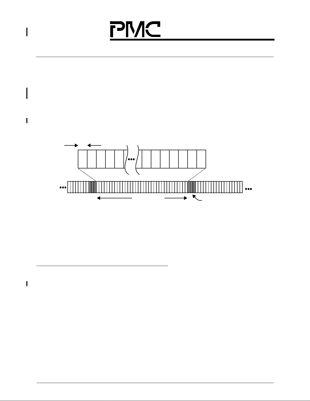
Figure 8. LCS Cell Sliced Across Dataslices and Crossbars
LCS Cell
LCS Header
(8 Bytes)
Payload
(64 Bytes)
Extra 12 bytes
(6 bytes per slice)
ETT1 Port
Dataslice
Slices 0,1
Dataslice
Slices 2,3
Dataslice
Slices 10,11
Dataslice
Slices 12,13
Crossbar 0
Crossbar 1
Crossbar 2
Crossbar 3
Crossbar 10
Crossbar 11
Crossbar 12
Crossbar 13
ETT1 Port
Dataslice
Slices 0,1
Dataslice
Slices 2,3
Dataslice
Slices 10,11
Dataslice
Slices 12,13
The 64 byte payload cell requires six Dataslices per port and 12 Crossbars (32 port, non-redundant). The
76 byte payload cell requires seven Dataslices per port and 14 Crossbars. The EPP is capable of
supporting the seventh Dataslice.
Because the extra data is obtained by slicing the cell then this does not affect the clock frequency of the
Chip Set. The onlyeffect is thatthe link between the ETT1 port and the linecard must go up from18 Gbaud
to 21 Gbaud. This is done by making the link wider, not faster.
1.2.9.2
8, 16, or 32 ports
The ETT1 core can supporta maximum of 32 ports. Smaller configurations can be supportedby simply not
using some of the ports. However, if the maximum system is an eight or 16 port configuration, then some
PROPRIETARY AND CONFIDENTIAL TO PMC-SIERRA, INC., AND FOR ITS CUSTOMERS’ INTERNAL USE 29
Page 34

Released
Data Sheet
PMC-2000164 ISSUE 3 ENHANCED TT1™ SWITCH FABRIC
PMC-Sierra, Inc.
PM9311/2/3/5 ETT1™ CHIP SET
cost savings can be achieved by using fewer Crossbar devices. A Crossbar can be configured to be in an
8- 16- or 32-port core, as shown in Table 1.
Table 1. Crossbar Configurations
Number of OC-192c ports
Number of Crossbars required
(non redundant)
Number of Crossbars required
(redundant)
1 to 8 3 + 1 Flow Control 6 + 2 Flow Control
9 to 16 6 + 1 Flow Control 12 + 2 Flow Control
17 to 32 12 + 2 Flow Control 24 + 4 Flow Control
The reduction in the number of crossbars is achieved by having a single port use more than one
connection on each Crossbar. In a 32 port system, each port will use one connection to each Crossbar
device; in an 8 port system,each port will use four connections on each Crossbar. (This DOES NOT apply
to Flow Control Crossbars; each port will always use only one connection.)
1.3 PRIORITIZED BEST-EFFORT QUEUE MODEL
The ETT1 switch core has been designed to maximize cell throughput while keeping latency small and
providing “fair” throughput among all ports. The ETT1 core supports four levels of strict priority. Level 0 is
the highest priority and level 3 the lowest. All conditions being equal, the core will always forward a higher
priority cell before a lower priority cell. Furthermore, the core will be fair to all inputs. This fairness is very
difficult to quantify and is onlymeaningful over time periods of many cells. Over short time periods (tens or
perhaps hundreds of cells) there may be temporary unfairness between ports.
A cell of a lower priority may pass a cell of a higher priority under certain conditions:
1. Since the scheduling pipeline is shorter for lower priorities, a cell of a lower priority may emerge
from the switch sooner than a cell of a higher priority if the lower-priority cell is sent immediately
after the higher-priority cell.
2. Hole requests for a higher priority can allow cells of a lower priority to pass cells of the higher
priority.
3. If the linecard responds to LCS grants faster than required to meet the system round trip time
constraint, then multicast cells of a lower priority may pass unicast cells of a higher priority, due to
a (programmable) delay in the EPP’s “Internal Delay Matching Adjustments” register.
4. In subport mode only: multicast output queues (VIQs) are shared by subports, so when a subport
is oversubscribed for an extended period of time, blocking may result on all subports . This
blocking of multicast can allow unicast cells of the same priority to pass.
In this section we describe the queueing model provided by the ETT1 switch core for this prioritized
best-effort traffic. We start by considering only OC-192c ports. The following sections describe how the
model differs for OC-48c ports.
30 PROPRIETARYAND CONFIDENTIAL TO PMC-SIERRA, INC., AND FOR ITS CUSTOMERS’ INTERNAL USE
Page 35

Released
Data Sheet
PMC-2000164 ISSUE 3 ENHANCED TT1™ SWITCH FABRIC
PMC-Sierra, Inc.
PM9311/2/3/5 ETT1™ CHIP SET
1.3.1 Unicast Traffic (OC-192)
Every ETT1 port has a separate request counter and ingress queue for each (output port, priority)
combination to which it can send unicast cells. In a full configuration, an ETT1 port can send to 32 ETT1
ports (including itself), at four priorities, and so willhave 128 unicast request counters and ingress queues.
All of these counters and queues are independent so that the switch does not suffer from head-of-line
blocking
Figure 9 illustrates the unicast ingress queueing model for one port.
The ingress queues are referred to as Virtual Output Queues (VOQs). This name indicates that each
queue holds cells going to just one output port.
Every ETT1 port also has the same number of unicast egress queues; one queue for every (input port,
priority) combination that can send cells to the port. Every port will have 128 unicast egress queues. It is
not acceptable to have a single egress queue per priority, as this can lead to gross unfairness between
ports. These egress unicast ports are called Virtual Input Queues (VIQs) as each queue only holds cells
that have come from a single input port. A useful model is to think of a VOQ as being directly connected
through the Crossbar to a single VIQ. The cell at the head of the VOQ is waiting to be scheduled in such a
way that it can move to the tail of the VIQ in the egress port.
1
.
Figure 9. The U nicas t Ingress Queueing Model for One Port
The associated ingress EPP is informed whenever an egress queue is full. In this case, the ingress port
will not issueany new requests to the Scheduler until sufficient cell spacebecomes available at the egress
queue. The transfer of cells from ingress to egress queues is lossless from a queueing perspective.
The best effort unicast ingress and egress queues can store up to 64 cells.
1.3.2 Multicast Traffic (OC-192)
The ETT1 core also supports multicast cells. Multicast cells are cells that must be forwarded to one or
more egress ports. The LCS header will indicate that a cell is multicast, and it will also contain a multicast
group identifier. The ETT1 port uses this identifier to determine the list of ports to which the cell should go.
This list of ports is called the multicast fanout. Different multicast groups will probably have different
fanouts.
The Scheduler arbitrates among unicast and multicast cells. A multicast cell of a given priority will always
have priority over a unicast cell of the same priority, all else being equal. Physical cell replication takes
place within the Crossbar.
1. Head -of-line blocking is a phenomenon encountered by input queued switches in thecase where a cell destined for one output port is delayed becaus e the cell at the head of the same FIFO queue is destined for some other output which is currently
congested.
PROPRIETARY AND CONFIDENTIAL TO PMC-SIERRA, INC., AND FOR ITS CUSTOMERS’ INTERNAL USE 31
Page 36

Released
Data Sheet
PMC-2000164 ISSUE 3 ENHANCED TT1™ SWITCH FABRIC
PMC-Sierra, Inc.
PM9311/2/3/5 ETT1™ CHIP SET
The Scheduler will not necessarily schedule all ports in a fanout at the same cell time. In other words, the
same multicast cell might pass through the Crossbar on several occasions before all egress ports have
received their copy of the cell.
Every ETT1 port has a single ingress queue and a single egress queue for multicast traffic at each priority,
as shown in Figure 10. (There are also request counters, as for unicast cells, but these are not shown.)
32 PROPRIETARYAND CONFIDENTIAL TO PMC-SIERRA, INC., AND FOR ITS CUSTOMERS’ INTERNAL USE
Page 37

Released
Data Sheet
PMC-2000164 ISSUE 3 ENHANCED TT1™ SWITCH FABRIC
Figure 10. Ingress and Egress Queue for Multi cast Traff ic
PMC-Sierra, Inc.
PM9311/2/3/5 ETT1™ CHIP SET
The Scheduler maintains information on the occupancy of the multicast ingress queues, and receives
backpressure/unbackpressure signals for the multicast egress queues. If an egress multicast queue is
backpressured then there is a question as to whathappens to the cell at the head of an ingress queue that
is trying to send to that backpressured egress queue (as well as other ports). If the Scheduler blocks the
ingress queue, then the system will experience head-of-line blocking for multicast cells at that priority.
Every ETT1 port can select how it wants to handle multicast cells that are sent to it. For each of the four
multicast egress queues, the local ETT1 CPU can either enable or disable a backpressure signal from
being sent to the Scheduler.
NOTE: This selection is at the egress queues, not the ingress queues.
If a port is set so that multicast backpressure is disabled, then that port will never cause head-of-line
blocking to occur in any ingress multicast queue that will send to it.
If a port is set so that multicast backpressure is enabled, then that port can assert a backpressure signal if
the egress queue gets too full. Consequently, this might cause head-of-line blocking at multicast ingress
queues that send cells to this port.
Therefore, head-of-line blocking is only guaranteed not to occur if allof the ports that can receive multicast
cells have their multicast backpressure signals disabled. If at least one port has backpressure enabled,
then head-of-line blocking might occur.
1.3.3 Unicast Traffic (Subport Mode)
The EPP can operate in one of two modes. The first mode uses the queueing model described previously,
and corresponds to a single channel of approximately 10 Gbit/s. The secondmode is called subport mode.
In subport mode an EPP can manage four channels of 2.5 Gbit/s each. The physical interface at the
Dataslice is always a single channel; in subport mode the four 2.5 Gbit/s channels are time multiplexed
onto the single 10 Gbit/s channel. More precisely, given that the ETT1 Chip Set always operates at 25M
cells per second, the subport mode correspond to four channels each of up to 6.25M cells per second.
Figure 11. shows the block diagram of an ETT1 port card. The six (or seven) Dataslices provide a single
interface. A separate MUX device is required to manage the four OC-48c channels and merge them so
they appear as a single channel to the EPP/DS.
PROPRIETARY AND CONFIDENTIAL TO PMC-SIERRA, INC., AND FOR ITS CUSTOMERS’ INTERNAL USE 33
Page 38

Released
Data Sheet
PMC-2000164 ISSUE 3 ENHANCED TT1™ SWITCH FABRIC
PMC-Sierra, Inc.
PM9311/2/3/5 ETT1™ CHIP SET
Figure 11. An ETT1 Port O perat ing in Subport Mode with Four OC-48c Linecards
OC-48c 0
OC-48c 1
OC-48c 2
OC-48c 3
MUX
ETT1 Port board
25M cell/s
interface
Dataslice 0/1
Dataslice 0/1
Dataslice 0/1
Dataslice 0/1
Dataslice 0/1
Dataslice 0/1
EPP
Crossbar
Crossbar
Crossbar
Crossbar
Crossbar
Crossbar
Scheduler
Flow Control
Crossbar
ETT1 Port board
The EPP can support all four best-effort priorities when operating in subport mode. This is the primary
feature that differentiates the EPPfromthe PP. Furthermore, the EPP can operate in a mixedmode switch,
so an ETT1 switch can have some ports operating in subport mode (quad OC-48c), while other ports
operate in normal mode (OC-192c).
NOTE: The EPP has been designed to operatewith the same Dataslicedevice as the PP, and this
has certain limitations that the designer should be aware of. The following sections on
subporting explain these limitations.
Ports are numbered 0 through 31and each port has one EPP. Subports are denoted as 0 through 3. Ports
with subports are shown as a (port, subport) pair; for example, port 4, subport 3 would be shown as (4,3)
Ports without subports (OC-192c) are simply numbered. The following queueing description assumes an
ETT1 core configured with all 32 ports in subport mode, supporting 128 OC-48c linecards.
First, consider a single priority. Figure 12 shows the 128 counters needed by one OC-48c linecard. There
are currently two requests outstanding for output (0,0). The ETT1 Chip Set uses virtual output queues to
avoid head-of-line blocking issues, therefore, the EPP needs to keep track of unicast requests going to
each one of the 128 possible output channels (0,0) through (31,3). Consequently, 128 counters are
needed. These counters reflect the outstanding requests that this one OC-48c ingress linecard has made
to the switch.
34 PROPRIETARYAND CONFIDENTIAL TO PMC-SIERRA, INC., AND FOR ITS CUSTOMERS’ INTERNAL USE
Page 39

Released
Data Sheet
PMC-2000164 ISSUE 3 ENHANCED TT1™ SWITCH FABRIC
PMC-Sierra, Inc.
PM9311/2/3/5 ETT1™ CHIP SET
Figure 12. The Input Request Counters
EPP
0,0
2
request
OC-48c linecard
grant
0,1
0
0,2
3
0,3
7
31,3
0
The EPP can support up to four OC-48c channels, and each channel must have its own set of request
counters for each of the 128 OC-48c output channels. Figure 13 shows the full set of counters for a single
priority.
Within the EPP an LCS Grant Manager process issues grants to the linecards in response to the received
requests. Onceper cell time theLCS Grant Manager selects one request counter to grant,given that many
may qualify. A request counter qualifies to receive a grant if the counter is non-zero and if there is at least
one empty cell buffer in the VOQ that is used for cells going to that particular output. Once the LCS Grant
Manager hasselected a particularVOQ, it decrements the corresponding counter and sends a grant to the
appropriate linecard.
The grant indicates a specific VOQ within the linecard. When the linecard receives the grant it does two
things. First, it sendsto theEPP the cell body that is currently at the head of the granted queue. Second, it
increments a local credit counter that is used to determine whether a new request for that queue can be
sent.
PROPRIETARY AND CONFIDENTIAL TO PMC-SIERRA, INC., AND FOR ITS CUSTOMERS’ INTERNAL USE 35
Page 40

Released
Data Sheet
PMC-2000164 ISSUE 3 ENHANCED TT1™ SWITCH FABRIC
PMC-Sierra, Inc.
PM9311/2/3/5 ETT1™ CHIP SET
Figure 13. Full Set of Counters for a Single Priority
OC-48c linecard
OC-48c linecard
OC-48c linecard
request
grant
request
grant
request
EPP
OC-48c 0
OC-48c 1
OC-48c 2
0,0
2
0,1
0
0,2
3
0,3
7
31,3
0
0,0
5
0,1
2
31,3
2
0,0
0
0,1
12
grant
31,3
0,0
15
0,1
31,3
OC-48c linecard
request
OC-48c 3
grant
36 PROPRIETARYAND CONFIDENTIAL TO PMC-SIERRA, INC., AND FOR ITS CUSTOMERS’ INTERNAL USE
7
8
3
Page 41

Released
Data Sheet
PMC-2000164 ISSUE 3 ENHANCED TT1™ SWITCH FABRIC
PMC-Sierra, Inc.
PM9311/2/3/5 ETT1™ CHIP SET
1.3.3.1 Virtual Output Queues
Ideally, the EPP/DS would have a separate VOQ which would correspond to each of the request counters.
This would mean that congestion on one VOQ would not impact any other VOQ on the same OC-48c or
any VOQs on different OC-48c channels.
In practice, the EPP is constrained by the amount of cell buffering available in the ETT1 Dataslice device
(which contains the actual cell buffers). Consequently, all four request counters that correspond to a single
output channel share a single queue, as shown in Figure 14.
The EPP only manages a single queue for each of the output channels (whether the output channel is
OC-48c or OC-192c). If the EPP is connected to four OC-48c inputs, then those four OC-48c linecards
must share the single queue used for each output. The four dotted arrows in Figure 14 show that the four
request counters for output (0,0) all map to the same VOQ for output (0,0).
PROPRIETARY AND CONFIDENTIAL TO PMC-SIERRA, INC., AND FOR ITS CUSTOMERS’ INTERNAL USE 37
Page 42

Released
Data Sheet
PMC-2000164 ISSUE 3 ENHANCED TT1™ SWITCH FABRIC
PMC-Sierra, Inc.
PM9311/2/3/5 ETT1™ CHIP SET
Figure 14. All R equ est Count ers for a Single Output Share a Sing le Queue
OC-48c
linecard
OC-48c
linecard
OC-48c
linecard
EPP
OC-48c 0
OC-48c 1
OC-48c 2
0,0
2
0,1
0
0,2
3
0,3
7
31,3
0
0,0
5
0,1
2
31,0
2
0,1
0
0,2
12
EPP
Virtual Output Queues (in the Dataslices)
(1 per output channel)
0,0
(This is for cells going
to output OC-48c
channel 0 on port 0)
0,1
0,2
0,3
1,0
1,1
1,2
1,3
31,0
31,1
31,2
31,3
OC-48c
linecard
31,3
7
0,0
15
0,1
8
OC-48c 3
31,3
3
38 PROPRIETARYAND CONFIDENTIAL TO PMC-SIERRA, INC., AND FOR ITS CUSTOMERS’ INTERNAL USE
Page 43

Released
Data Sheet
PMC-2000164 ISSUE 3 ENHANCED TT1™ SWITCH FABRIC
PMC-Sierra, Inc.
PM9311/2/3/5 ETT1™ CHIP SET
The complete sequence of events at the input side is shown in Figure 15.
1. Linecard a issues a request to the EPP to send a cell to output channel (0,1). The initial request
count is zero, so the arrival of the request then increments the request count to one.
2. The LCS GrantManager sees that thereis at leastone empty cell buffer in the virtual output queue
for output (0,1), and that the request counter for (0,1) is non-zeroand so it decrements the request
counter (back to zero) and issues a grant to the linecard.
3. The linecard then forwards the actual cell body to the EPP which stores the cell in the virtual
output queue. The EPP also issues a request to the Scheduler, indicating that there is a cell
waitingtobetransferredtooutput(0).
4. Later the Scheduler issues a grant to the EPP which can forward the cell through the Crossbar to
the output channel (the EPP at port 0).
PROPRIETARY AND CONFIDENTIAL TO PMC-SIERRA, INC., AND FOR ITS CUSTOMERS’ INTERNAL USE 39
Page 44

Released
Data Sheet
PMC-2000164 ISSUE 3 ENHANCED TT1™ SWITCH FABRIC
PMC-Sierra, Inc.
PM9311/2/3/5 ETT1™ CHIP SET
Figure 15. Sequence of Events at the Input Side
OC-48c
linecard
OC-48c
linecard
Request (0,1)
EPP
Initial state. Subport 0 has no outstanding requests for output (0,1)
EPP
OC-48c 0
0,0
2
0,1
0
0,2
3
0.3
7
OC-48c 0
0,0
2
0,1
1
0,2
3
0.3
7
Virtual Output Queues
0,0
0,1
0,2
0,3
Virtual Output Queues
0,0
0,1
0,2
0,3
Crossbar
Scheduler
Crossbar
Scheduler
Subport 0 issues a request to send a cell to output (0,1).
The request count for output (0,1) is incremented.
OC-48c
linecard
EPP
Grant (0,1)
The LCS Grant Manager issues a grant for queue (0,1) to subport 0.
OC-48c 0
0,0
2
0,1
1
0,2
Manager
3
0.3
7
Virtual Output Queues
LCS
Grant
0,0
0,1
0,2
0,3
40 PROPRIETARYAND CONFIDENTIAL TO PMC-SIERRA, INC., AND FOR ITS CUSTOMERS’ INTERNAL USE
Crossbar
Scheduler
Page 45

Released
Data Sheet
PMC-2000164 ISSUE 3 ENHANCED TT1™ SWITCH FABRIC
PMC-Sierra, Inc.
PM9311/2/3/5 ETT1™ CHIP SET
Figure 15. (Continued)
OC-48c
linecard
OC-48c
linecard
EPP
Linecard a receives the grant and forwards ce ll body to go to output (0,1).
EPP
OC-48c a
0,0
2
0,1
0
0,2
3
0.3
7
A request is made to the Scheduler.
OC-48c a
0,0
2
0,1
1
0,2
3
0.3
7
Virtual Output Queues
0.0
0,1
0,2
0,3
Virtual Output Queues
0,0
0,1
0,2
0,3
Request (0)
Grant (0
Crossbar
Scheduler
Crossbar
Scheduler
The EPP then sends the cell through the crossbar to the output queue of port 0
The Scheduler issues a grant to queue (0,1).
.
The departure of a cell from the VOQ will mean that there is now space for at least one more cell in that
VOQ, and that could trigger the LCS Grant Manager to issue a new grant, assuming that a new request
had come in for that queue.
1.3.3.2
The Output Process
Each EPP consists of an input (i)EPP and an output (o)EPP. The request counters and virtual output
queues described above all reside in the iEPP . The oEPP has virtual input queues that receive the cells
forwarded via the Crossbar.
PROPRIETARY AND CONFIDENTIAL TO PMC-SIERRA, INC., AND FOR ITS CUSTOMERS’ INTERNAL USE 41
Page 46

Released
Data Sheet
PMC-2000164 ISSUE 3 ENHANCED TT1™ SWITCH FABRIC
PMC-Sierra, Inc.
PM9311/2/3/5 ETT1™ CHIP SET
In the ideal scenario, each oEPP would have a separate virtual input queue for every (possibly 128) input
channel. However, the same restriction applies, limiting the oEPP to just 32 queues per output OC-48c
(and per priority). Figure 16 shows the virtual input queues in each oEPP when attached to four OC-48c
ports.
Each virtual input queue maps back to a single virtual output queue in one of the iEPPs. In abstract terms,
the virtual input queue is simply an extension of the appropriate virtual output queue.
Each output OC-48c channel within the oEPP has its own set of unicast virtual input queues. If an output
queue (virtual input queue) is backpressured, then this will push back to the appropriate virtual output
queue. However, each virtual output queue is shared by the four input OC-48c channels within that iEPP,
so backpressuring a virtual output queue has the effect of asserting backpressure to all four OC-48c’s on
thesameiEPP.
The oEPP has an Output Scheduler process which determines which cell should be forwarded to the
egress linecards.
42 PROPRIETARYAND CONFIDENTIAL TO PMC-SIERRA, INC., AND FOR ITS CUSTOMERS’ INTERNAL USE
Page 47

Released
Data Sheet
PMC-2000164 ISSUE 3 ENHANCED TT1™ SWITCH FABRIC
PMC-Sierra, Inc.
PM9311/2/3/5 ETT1™ CHIP SET
Figure 16. Virtual Input Queues
iEPP port 0
iEPP port 1
VOQ 0,0
VOQ 0,1
VOQ 0,2
VOQ 0,3
VOQ 31,3
VOQ 0,0
VOQ 0,1
VOQ 0,2
VOQ 0,3
0
31
oEPP port 0Virtual Input Queues
0
1
output
OC-48c 0
31
0
1
output
OC-48c 1
iEPP port 31
VOQ 31,3
VOQ 0,0
VOQ 0,1
VOQ 0,2
VOQ 0,3
VOQ 31,3
1
31
0
1
31
output
OC-48c 2
output
OC-48c 3
PROPRIETARY AND CONFIDENTIAL TO PMC-SIERRA, INC., AND FOR ITS CUSTOMERS’ INTERNAL USE 43
Page 48

Released
Data Sheet
PMC-2000164 ISSUE 3 ENHANCED TT1™ SWITCH FABRIC
PMC-Sierra, Inc.
PM9311/2/3/5 ETT1™ CHIP SET
1.3.3.3 Four P rioritie s
The description in the preceding sections only considered a single priority. The EPP supports four
priorities. Therefore, there are four times as many counters and queues as have been described so far ,
and this is only for unicast traffic. The four priorities can be modeled as separate planes; the input and
output queue figures shown earlier can be considered as 2-D planes. The four priorities are then four
copies of these planes, stacked next to each other in a third dimension. Figure 17illustrates this model for
the reference counters and virtual output queues. The virtual input queues at the oEPP are not shown.
Consequently, each iEPP has 2048 request counters (4 OC-48c input channels * 128 output channels * 4
priorities) and 512 virtual output queues (128 outputs * 4 priorities). Each oEPP has 512 virtual input
queues (4 output channels * 32 ports * 4 priorities). Remember, this calculation is for the configuration of
128 ports of OC-48c. Later on we describe how the number of queues and request counters differs for
some other possible configurations.
44 PROPRIETARYAND CONFIDENTIAL TO PMC-SIERRA, INC., AND FOR ITS CUSTOMERS’ INTERNAL USE
Page 49

Released
Data Sheet
PMC-2000164 ISSUE 3 ENHANCED TT1™ SWITCH FABRIC
PMC-Sierra, Inc.
PM9311/2/3/5 ETT1™ CHIP SET
Figure 17. The Four Priorities
OC-48c 0
OC-48c 1
OC-48c 2
OC-48c 3
OC-48 a
OC-48 a
31,3
OC-48 b
OC-48 b
31,3
OC-48 c
OC-48 c
12
32d
OC-48 d
15
OC-48 d
32d
0,0
OC-48c a
2
0,1
0
0,2
3
0,3
7
32d
0
OC-48c b
0,0
5
0,1
2
32d
2
OC-48c c
1a
0
1b
32d
7
OC-48c d
1a
1b
8
32d
3
12
15
0,0
2
1b
0
1c
3
1d
7
0
1a
5
1b
2
2
1a
0
1b
7
1a
1b
8
3
0,0
2
1b
0
1c
3
1d
7
32d
0
1a
5
1b
2
32d
2
1a
0
1b
12
32d
7
1a
15
1b
8
32d
3
0,0
2
1b
0
1c
3
1d
7
32d
0
1a
5
1b
2
32d
2
1a
0
1b
12
32d
7
1a
15
1b
8
32d
3
1,1
1,2
1,3
31,0
31,1
31,2
31,3
0,0
0,1
0,2
0,3
1,0
32a
32b
32c
32d
1a
1b
1c
1d
2a
2b
2c
2d
Priority 0
1a
1b
1c
1d
2a
2b
2c
2d
32a
32b
32c
32d
Priority 3
Priority 2
Priority1
1a
1b
1c
1d
2a
2b
2c
2d
32a
32b
32c
32d
1.3.3.4 Multiplexing Scheduler Requests and Grants.
Figure 16 and Figure 17 imply that the ETT1 Scheduler can accept requests from each of the 32 ports
where a request specifies one of 128 output channels. This is not the case; the Scheduler only maintains
information on a port basis, not a subport basis.
PROPRIETARY AND CONFIDENTIAL TO PMC-SIERRA, INC., AND FOR ITS CUSTOMERS’ INTERNAL USE 45
Page 50

Released
Data Sheet
PMC-2000164 ISSUE 3 ENHANCED TT1™ SWITCH FABRIC
PMC-Sierra, Inc.
PM9311/2/3/5 ETT1™ CHIP SET
Consequently, the requests associated with cells going to subports (0,0), (0,1), (0,2) and (0,3) are
amalgamated to become requests for port 0.
NOTE: The channel information is not lost; a cell going to channel (0,1) will still be delivered to
channel 1, port 0. However, the four queues have their requests multiplexed over a single
request/grant connection. Figure 18 illustrates this concept.
Figure 18. Scheduler Requests/Grants are Multiplexed at a Port Level
VOQs in iEPP
cells for output subport (0,0)
cells for output subport (0,1)
cells for output subport (0, 2)
cells for output subport (0,3)
Request to send to port 0
Scheduler
Grant to send to port 0
The EPP has two decisions to make: which request to issue, and which of the four queues to grant.
At any cell time, the iEPP may have several possible new requests which it must communicate to the
Scheduler. The iEPP has a Scheduler Request Modulator which makes this decision. See Section 3.1.3
“Scheduler Request Modulator” on page 158 for a discussion of this algorithm.
When the iEPP receives a grant from the Scheduler it must decide which of the four VOQs should be
serviced. A simple round-robin algorithm is used (across non-empty queues).
1.3.4 Multicast Traffic (subport mode)
Multicast cells are handled at a port level, not a subport level. There is a single cell queue within the iEPP,
for each priority of multicast cells. EachOC-48c channel has its own requestcounter, but, likethe unicasts,
these four request counters map to a single virtual output queue (per priority), as shown in Figure 19.
46 PROPRIETARYAND CONFIDENTIAL TO PMC-SIERRA, INC., AND FOR ITS CUSTOMERS’ INTERNAL USE
Page 51

Released
Data Sheet
PMC-2000164 ISSUE 3 ENHANCED TT1™ SWITCH FABRIC
PMC-Sierra, Inc.
PM9311/2/3/5 ETT1™ CHIP SET
Figure 19. Each iEPP has a Sin gle Vi rt ual Output Que ue for Multicas t Cells
OC-48c 0
OC-48c 1
OC-48c 2
OC-48c 3
OC-48c 0
OC-48c 1
OC-48c 2
OC-48c 3
m
2
m
5
m
0
m
4
iEPP
Priority 0
multicast cells
As before, this single queue is nota limitation unless backpressure is asserted to thequeue, in which case
all four OC-48c subports are backpressured for all multicast cells from this port at this priority.
ETT1 uses a multicast tag in the LCS header to identify the multicast group that this cell should go to. The
iEPP then maps the tag into a port vector with one bit per port. This port vector is then passed to the
Scheduler to indicate the list of portsthat should receive this multicast cell. Again, the Scheduler only
recognizes 32 ports and not 128 OC-48c subports;at the input side,a multicast cell destined for any one of
output ports (0,0), (0,1), (0,2) or (0,3) would simply be forwarded to the oEPP at port 0.
The oEPP receives the multicast cell, together with its tag. It then maps the (tag, source_port) into a new
4-bit vector that identifies what combination of the four subports should receive this multicast cell.
Figure 20 shows the entire process.
multicast
tag
12
iEPP
Input Multicast
Fanout Table
Figure 20. Multicast Cell Processing
Crossbar
Scheduler
32
multicast
src
tag
prt
17
Output Scheduler
oEPP
Output Multicast
Fanout Table
4
PROPRIETARY AND CONFIDENTIAL TO PMC-SIERRA, INC., AND FOR ITS CUSTOMERS’ INTERNAL USE 47
Page 52

Released
Data Sheet
PMC-2000164 ISSUE 3 ENHANCED TT1™ SWITCH FABRIC
PMC-Sierra, Inc.
PM9311/2/3/5 ETT1™ CHIP SET
In order to reduce the blocking effects of one OC-48c channel over another channel on the same port,
there is a special multicast output queue for each priority. The multicast cells forwarded through the
Crossbar are still queued in the order they arrive. This special queue enables cells to be sent out-of-order,
but will always be sent in-order for a given egress subport. Therefore, a multicast cell waiting in the output
queue memory can only be blocked by cells destined to the same egress subport. Additional output queue
memory becomes available whenever a cell is dequeued.
If backpressureis assertedby one of the OC-48c channels to theoutput multicast queue, thensubsequent
cells going to other channels on the same port may be blocked if the entire queue is occupied by cells
destined to the blocked OC-48c channel. This is a consequence of sharing the output queue memory
allocation for multicast cells at a given priority. This can cause multicast backpressure to the central
Scheduler which can block multicast cells destined to other ports at the same priority if multicast
backpressure is enabled.
1.3.4.1
Multicast Tables (OC-192c and Quad OC-48c Modes)
The input multicast fanout table (EITIBM in the EPP) is always used for multicast cells. Every EPP has its
own EITIBM table with 4096 entries. The EPP uses the 12-bit multicast tag field from the LCS label field to
determine which entry in the table should be used for each multicast cell, as shown in Figure 21. Each
entry is simply a 32 bit vector where a 1 means that the cell should go to thatport. So if an entry has a 1 at
bit 12, for example, then a multicast cell that uses that entry will be sent to port 12 (as well as any other
ports that have their bit set to 1).
Figure 21. EITIBM structure
iEPP
Input Multicast
Fanout Table EITIBM
0
Multicast tag [11:0]
12
4095
To Scheduler
32
31
1 bit for each output OC-192c port
0
48 PROPRIETARYAND CONFIDENTIAL TO PMC-SIERRA, INC., AND FOR ITS CUSTOMERS’ INTERNAL USE
Page 53

Released
Data Sheet
PMC-2000164 ISSUE 3 ENHANCED TT1™ SWITCH FABRIC
PMC-Sierra, Inc.
PM9311/2/3/5 ETT1™ CHIP SET
The output multicast fanout table (EOTIBM in the EPP) is only used if the port is in quad OC-48c mode. In
quad OC-48c mode a multicast cell arrives at the oEPP via the crossbar. The oEPP must determine what
combination of the four OC-48c ports that this multicast cell should be forwarded to (15 possible
combinations assuming it goes to at least one of the ports). The oEPP has the multicast tag (12 bits) from
the label, but that is not sufficient. It is not sufficient because the multicast tags are managed
independently across all ports: each iEPP has its own EITIBM and so a given 12 bit multicast tag might be
used to specify different multicast fanouts for two differentiEPPs. To resolve the ambiguity,the oEPPmust
also include the source port number with the 12 bit multicast tag, and combines the 5 bit source port with
the 12 bit multicast tag to produce a 17 bit tag thatis unique across the entire fabric. This can then be used
to index into a table of 4-bit entries as shown in Figure 22.
Figure 22. OITIBM structure
oEPP
Output Multicast
Fanout Table EOTIBM
0
Multicast tag [11:0]
Source port[4:0]
17
3
1 bit for each o f the four local OC-48c ports
0
131071
4
To Output
Scheduler
The index is the combination of {Multicast_tag, source_port}, so that the source port forms the least
significant bits of the address (index). Each entry has fourbits such that bit 0 corresponds to subport 0 and
bit 3 corresponds to subport 3.
1.3.5 Combinations of OC-192c andQuadOC-48c Linecards
A switch might contain both OC-192c ports and quad OC-48c ports. Each port card must be configured
with information about all of the cards. The number of ingress queues is a function of this mix of ports:
given n quad OC-48c ports and m OC-192c ports, then each port will have U unicast queues, where:
U = 4 priorities * n * 4 egress subports + 4 priorities * m
So if n = 32 and m = 0 then U = 512.
PROPRIETARY AND CONFIDENTIAL TO PMC-SIERRA, INC., AND FOR ITS CUSTOMERS’ INTERNAL USE 49
Page 54

Released
Data Sheet
PMC-2000164 ISSUE 3 ENHANCED TT1™ SWITCH FABRIC
PMC-Sierra, Inc.
PM9311/2/3/5 ETT1™ CHIP SET
If a port is operating in OC-192c mode then it will also have U unicast request counters. If a port is
operating in quad OC-48c mode then it will have 4 * U unicast request counters - a separate set of request
counters for each of the OC-48c linecards.
Each port always has four multicast ingress queues.
The number of egress queues is a function of the mode of the port itself, not the other ports: a port in
OC-192c mode will have one queue for each input port and priority, or 4 * 32 = 128 egress queues. A port
in quad OC-48c mode will have four times as many queues, or 512 queues.
Each port always has four multicast egress queues.
The size and depth of all request counters and queues are defined in Section 3.2 “Input Dataslice Queue
Memory Allocation with EPP” on page 162 and Section 3.3 “Output Dataslice Queue Memory Allocation
with EPP” on page 162.
1.3.6 Summary
Every ETT1 port has a number of ingress request counters and queues as well as egress queues. Given
support for 32 ports, four subports per port, and four priorities, then there are up to 512 unicast ingress
queues and four multicast ingress queues, and the same number of egress queues.
At every cell time, the Scheduler arbitrates among all of the ingress queues that are eligible to forward a
cell through the Crossbar. An ingress queue iseligible if it is non-empty and its destination egress queue is
not backpressured. The Scheduler makes its decision using absolute priorities, with multicast requests
having precedence over unicast requests at the same level, as shown in Figure 23.
Figure 23. Scheduler Priorities
Best Effort Traffic
Priority 0 Multicast
Priority 0 Unicast
Priority 1 Multicast
Priority 1 Unicast
Priority 2 Multicast
Priority 2 Unicast
Priority 3 Multicast
Priority 3 Unicast
Highest precedence
Lowest precedence
50 PROPRIETARYAND CONFIDENTIAL TO PMC-SIERRA, INC., AND FOR ITS CUSTOMERS’ INTERNAL USE
Page 55

Released
Data Sheet
PMC-2000164 ISSUE 3 ENHANCED TT1™ SWITCH FABRIC
PMC-Sierra, Inc.
PM9311/2/3/5 ETT1™ CHIP SET
1.3.7 The LCS Protocol
In this section, we describe the LCS protocol from a functional perspective and explain how it works with
the queueing model that was described in the previous section.
NOTE: The LCS protocol is defined in the “LCS Protocol Specification -- Protocol Version 2”,
available from PMC-Sierra,Inc. This version of LCS supersedes LCS Version 1. Version 2
is first supported in the TT1 Chip Set with the Enhanced Port Processor device (also
referred to as the ETT1 Chip Set) and will be supported in future PMC-Sierra products. A
comparison of the two versions of the LCS protocol is in the same document.
The primary role of the LCS protocol is as a credit-based flow control mechanism that ensures that cells
are transferred between the linecard and the switch core only when sufficient buffer space is available. In
order to do this, the linecard must have knowledge of the queues that exist in the ETT1 core. The LCS
protocol is an asymmetrical protocol; we will first consider the ingress direction. Figure 24 shows the 132
best effortingress queues inan ETT1 port (this assumes an all-OC-192c switch). The linecard may have a
very different number of queues (typically many more), and thus must map its own internal queues to the
physical queues present in the ETT1 core.
Figure 24. ETT1 Port Ingress Queues
LCS Header
ETT1 Port
128 unicast
4multicast
linecard
ingress
queues
Linecard
Mapping
128 unicast
4multicast
Payload
Cell requests and payloads
Credit Information
For example, the linecard might provide an ATM interface which can manage many thousands of virtual
circuit flows, and might have a separate internal queue for each flow. The linecard must map its own
ingress queues to the 132 ingress queues present in theETT1 port.The 132 queues shown in the linecard
do not have to be physically implemented provided that the linecard can perform the requisite mapping
from linecard queues to ETT1 queues on-the-fly. The ETT1 ingress queues areVirtual Output Queues; the
mapping function simply has to map each linecard queue to the desired egress port within the ETT1 core.
The mapping function must also select the appropriate priority if more than a single priority is required.
PROPRIETARY AND CONFIDENTIAL TO PMC-SIERRA, INC., AND FOR ITS CUSTOMERS’ INTERNAL USE 51
Page 56

Released
Data Sheet
PMC-2000164 ISSUE 3 ENHANCED TT1™ SWITCH FABRIC
PMC-Sierra, Inc.
PM9311/2/3/5 ETT1™ CHIP SET
Figure 24 shows ingress cell requests and data cells being forwarded to the ETT1 port. These cells are of
a fixed size and format: an LCS cell consists of an eight byte LCS header followed by a fixed length
payload. The payload can be 64or 76 bytes (dependingon the numberof Dataslices and Crossbarsused),
but all ports in the switch must use the same size payload. The TT1 Chip Set never examines or modifies
the cell payload unless the cell is used for internal control purposes.
The linecard can send a new cell request whenever a new cell arrives at the linecard and the linecard has
at least one request credit remaining for the appropriate queue. So the linecard must keep track of the
number of outstanding requests that it can send, and must not issue a request unless it has a
corresponding credit.
The ETT1 port returns grant/credit information to the linecard. This grant/credit information reflects the
occupancy of the ingress queues in the ETT1 port. The linecard can only send a cell to a given ingress
queue within the ETT1 port when it receives a grant from the ETT1 port. The linecard increments its
corresponding credit counter when it receives a grant/credit.
In order to sustain the maximum possible throughput, the linecardmust beable tosend a new cell within a
short time of receiving a grant/credit from the ETT1 port. If the linecard cannot do this then the VOQ at the
ingress ETT1port may become empty which might, in turn, affectthe throughput of the switch.The system
designer must be aware of the time budget that is really available to the linecard devices.
The grant/credit mechanism is notused in the egress direction. Rather, a simpler Xon/Xoff-like mechanism
is used. The oEPP will forward cells to the egress linecard whenever it has cells waiting in its output
queues. The linecard can request the EPP to not send a cell of a given priority, or any combination of
priorities, by asserting the hole request bits in the LCS header. If a hole request bit is asserted at a given
priority, then it is a request from the linecard to the EPP that the EPP should not forward a cell of that
priority at one cell time in the future. The time between theEPP receiving the hole request and observing it
is guaranteedtobeno more than 64 cell times.Future LCS compliant productswill have different response
times. Linecard designs requiring backpressure features should accommodate all LCS products to which
they will attach.
If a linecard has nearly exhausted its egress buffers for priority 2 cells, then it might continuously assert
hole request for priority 2 until it can recover some additional buffers.
NOTE: The hole request mechanism operates per-priority and not per-source port.
Refer to the “LCS Protocol Specification - Protocol Version 2”, available from PMC-Sierra, Inc., for further
details on the LCS protocol and the definition of the various fields used within the LCS header in each
direction.
1.4 EXPLICIT BACKPRESSURE FROM OEPP TO IEPP
The iEPP does not make a unicast request to the Scheduler unless the destination VIQ has a sufficient
number of empty buffers. For each unicast egress VIQ there is one corresponding ingress VOQ. Every
iEPP maintains state information on the occupancy of the relevant egress VIQs in all of the EPPs
(including itself) in order to ensure that it does not forward a cell to a full VIQ.
52 PROPRIETARYAND CONFIDENTIAL TO PMC-SIERRA, INC., AND FOR ITS CUSTOMERS’ INTERNAL USE
Page 57

Released
Data Sheet
PMC-2000164 ISSUE 3 ENHANCED TT1™ SWITCH FABRIC
PMC-Sierra, Inc.
PM9311/2/3/5 ETT1™ CHIP SET
The actual occupancy of a VIQ is dynamic: the number of free cell locations will increment whenever a cell
is forwarded to the attached linecard,and the number of free cell locations will decrement whenever a new
cell enters the VIQ from the crossbar. The iEPP knows the latter information - it is the iEPP that forwards
the cellto the VIQ. But the iEPP does not know when a cell getssentout to the linecard.SotheoEPP must
tell each iEPP how many cells have been sent from each relevant VIQ, and this information must be sent
with sufficient frequency that the throughput of a single flow is not adversely affected.
In the ETT1 fabric, this update information is transmitted from the oEPPs to the iEPPs via a second
Crossbar, referred to as the Flow Control Crossbar. Figure 25 shows the cell flow from left to right and the
reverse flow of the update information.
Figure 25. A S eparate Cross bar is Used to Convey Backpressure Informati on to the iEPPs
Virtual Output Queues
iEPP
0,0
0,1
0,2
0,3
Cell
Crossbar
Req/Gnt
Scheduler
sync
Flow Control
Crossbar
Virtual Input Queues
0,0
0,1
0,2
0,3
oEPP
Every iEPP maintains a set of counters (Output Queue Debit Counters) that track the number of cells in
each of the relevant VIQs of every oEPP. At reset, these counters are all set to zero. A counter is
incremented whenever the iEPP makes a request to forward a cell to the appropriate VIQ. If the counter
reaches a pre-determined maximum, then the iEPP will not issue further requests. Once some cells are
forwarded from the VIQ, the iEPP will reduce the counter and resume issuing requests for that flow.
In general, the user does not need to be aware of the details of this mechanism except for the case when
update information is lost,perhaps due to a noise-induced error on one ormore of the links attached to the
Flow Control Crossbar. The details of this error recovery mechanism are described in Section “Enhanced
Port Processor - Flow Control Crossbar” on page 94.
PROPRIETARY AND CONFIDENTIAL TO PMC-SIERRA, INC., AND FOR ITS CUSTOMERS’ INTERNAL USE 53
Page 58

Released
Data Sheet
PMC-2000164 ISSUE 3 ENHANCED TT1™ SWITCH FABRIC
PMC-Sierra, Inc.
PM9311/2/3/5 ETT1™ CHIP SET
1.4.1 Flow C ontrol Crossbar Synchronization
The Flow ControlCrossbars interconnect every EPP with every other EPP. During each cell time, the Flow
Control Crossbar sets the crosspoints such that every iEPP receives update information from one other
oEPP. Further, no two iEPPs receive the same update information from the same oEPP. In the next cell
time the crosspoints must be re-organized so that every iEPP receives update information from a different
oEPP.
The system must ensure that theFlow Control Crossbars and the EPPsareall synchronized, so that every
iEPP knows from which oEPP it is receiving information at any given time. This synchronization
information is generated by the Scheduler using the FCCSYN register to send a periodic pulse out to all
EPPs. Further, if a redundant Scheduler is used then the two Schedulers must be synchronized. This
Scheduler-to-Scheduler synchronization occurs after a Scheduler Refresh operation. Refer to Section
1.9.4 “Scheduler Refresh Procedure” on page 98.
1.5 TDM SERVICE
The TDM service enables linecards to periodically reserve bandwidth within the ETT1 core. Cells that are
switched via this service will have a fixed latency through the switch and will not be delayed due to best
effort contention for an output port. 1-in-N idle cells and egress control packets may cause temporary
delays, but these should be absorbed by the guardband and speedup.
The TDM service is implemented within the ETT1 core using:
• dedicated queues in the ETT1 ports
• a table-based reservation mechanism in the ETT1 ports
• a flexible synchronization mechanism
1.5.1 TDM Queues
The linecard uses the normal LCS request-grant mechanism for TDM cells. When TDM cells arrive at an
ETT1 ingress port, they are queued in a single TDM queue which can buffer up to 96 cells. The cells are
stored in the ingress queue until their reservation time occurs, at which time they are forwarded through
the crossbar to the appropriate egress TDM queue. Given that there can be no contention for TDM cells
then a TDM queue might seem unnecessary. The queue is present so that the linecard does not need to
be closely synchronized with the ETT1 fabric.
If the port is operating in subport mode then four ingress queues are used, one for each subport. Each
ETT1 port has a single egress TDMqueue, evenwhen theport is in subport mode. The ETT1 can transmit
cells out-of-order between the subports, and so a single shared TDM queue does not cause a problem.
Figure 26 illustrates the queueing structure.
54 PROPRIETARYAND CONFIDENTIAL TO PMC-SIERRA, INC., AND FOR ITS CUSTOMERS’ INTERNAL USE
Page 59

Released
Data Sheet
PMC-2000164 ISSUE 3 ENHANCED TT1™ SWITCH FABRIC
PMC-Sierra, Inc.
PM9311/2/3/5 ETT1™ CHIP SET
Figure 26. The Queueing Structure
ETT1 Core
Linecard
Ingress
TDM
queue
LCS credits
ETT1 port
Ingress
TDM
queues
ETT1 port
r
a
b
s
s
o
r
C
1
T
T
E
Egress
TDM
queue
Linecard
Egress
TDM
queue
Figure 26 also highlights some important points with respect to the TDM service:
• The linecard may also require a TDM ingress and egress queue. Unless the arrivalof TDM cells at
the linecard is synchronized with the start of the TDM Frame, the linecard will need to buffer those
cells until the appropriate time.
• There is no backpressurefrom the ETT1 egressTDM queue. Backpressureisnot meaningful for a
TDM service within the ETT1 core. The egress linecard must accept TDM cells that are sent to it
(or else discard them).
• The normal LCS credit mechanism is used for ingress TDM cells.
1.5.2 TDM Reservation Tables
The TDM service operates by enabling ports to reserve bandwidth through the ETT1 crossbar at specific
times. Each port has two logically separate tables; one for sending and one for receiving TDM cells. The
Send and Receive tables are physically implemented in a single table called the TDM table. This TDM
table has 1,024 entries, although fewer entries can be used if the Frame length is less than 1024. Each
entry is of the form shown in Table 2.
Table 2. TDM Reservation Table
Field Size (bits) Meaning
Input VLD 1 1 if the input side TDM entry is valid
Input Tag 10 Tag for incoming cells (TDM flow ID)
PROPRIETARY AND CONFIDENTIAL TO PMC-SIERRA, INC., AND FOR ITS CUSTOMERS’ INTERNAL USE 55
Page 60

Released
Data Sheet
PMC-2000164 ISSUE 3 ENHANCED TT1™ SWITCH FABRIC
Table 2. TDM Reservation Table (Continued)
PMC-Sierra, Inc.
PM9311/2/3/5 ETT1™ CHIP SET
Field Size (bits) Meaning
Subport 2 Identifies the source subport (if in subport mode, else 0)
Output
VLD
1 1 if the output side TDM entry is valid
Input Port 5 Input port that the output expects to receive from
Output
vector
4
A four-bit vector which defines the fanout of the subports that should receive
aTDMcell.
The EPPcontains two TDM tables so that one table can be usedby the fabric while the system software is
configuring the other table. All EPPs must use the same table at the same time. A TDM LCS Control
Packet is used to specify which of the two tables is being used at any given time.
At thestart of the Frame, a TDM pointer in each port begins at entry 0 in the table and advances one entry
every cell time. During everycell time,if the “current” TDM table Send entry is valid, the EPP checks to see
if the cell at the head of the appropriate TDM queue has a TDM flow ID (tag) that matches the entry in the
table. If not, then nothing special is done. If they do match then the EPP informs the Scheduler that it will
be sendinga TDM cell at some fixed time in the future.Thisprevents the Scheduler fromtryingto schedule
a best-effort cell from that port at the same time. Figure 27 shows the logic at the ingress port.
56 PROPRIETARYAND CONFIDENTIAL TO PMC-SIERRA, INC., AND FOR ITS CUSTOMERS’ INTERNAL USE
Page 61

Released
Data Sheet
PMC-2000164 ISSUE 3 ENHANCED TT1™ SWITCH FABRIC
PMC-Sierra, Inc.
PM9311/2/3/5 ETT1™ CHIP SET
Figure 27. Ingress Port Logic
TDM Cell Queues
OC-48c 0
OC-48c 1
OC-48c 2
OC-48c 3
=?
“Send”Table
OC-48c Select
TDM Identifier
0
Current TDM Slot Time
991
The egress side of the port also looks at the TDM table. If the Output Valid bit in the current entry is set,
then the port tells the Scheduler that it expects to receive a TDM cell at some fixed time in the future. This
prevents the Scheduler from trying to schedule a best-effort cell to that port at the same time.
If the Scheduler doesn’t receive the input TDM request bit from the specified input port, then it assumes
that there is no TDM cell ready to be transmitted, and thus any egress port that expected to receive that
cell will now become available for best-effort cell scheduling.
When the TDM cell enters the egress port, it is placed in a separate, 96-entry, egress queue dedicated for
TDM traffic. Whenever this queue is non-empty, the cell at the head of the queue is sent immediately to the
linecard (provided that the Output Scheduler is not frozen).
PROPRIETARY AND CONFIDENTIAL TO PMC-SIERRA, INC., AND FOR ITS CUSTOMERS’ INTERNAL USE 57
Page 62

Released
Data Sheet
PMC-2000164 ISSUE 3 ENHANCED TT1™ SWITCH FABRIC
PMC-Sierra, Inc.
PM9311/2/3/5 ETT1™ CHIP SET
The TDM service is inherently a multicastservice. Theegress ETT1must thereforesupport the ability for a
TDM cell to go to any combination of the four subports within a port. A four-bit field in every TDM table
entry provides the multicast fanout for each TDM cell that is received at the egress port. The EPP keeps
track of this fanout information and sends the TDM cell to each subport that is a member of the fanout.
Figure 28 illustrates how the EPP uses the TDM table to determine the source port of a TDM cell, as well
as the local subport multicast fanout.
Figure 28. The oE PP Must Treat the Transfer red TDM Cell as a Multicast Cell
Cell from Crossbar
To S cheduler
TDM Reservation Table
0 991
Current TDM Slot Time
Inputport=12
output vector
= 0101
(multicast fanout)
Output TDM Cell Queue
000101110101
The output TDM cell queue does not need to be large as TDM cells are always forwarded to the output
linecards at the highest priority, and the TDM queue is never backpressured. The size of this queue does,
however, restrict the possible TDM table configuration. The following constraints are required to prevent
dropped TDM cells:
• In a TDM table time slot, an input port cannot send more than one cell and an output port can not
receive more than one cell.
• Subport mode:The TDM ReservationTable can specify thesame ingress subport only once every
four time slots.
• Subport mode: The TDM Reservation Table can not specify the same egress subport more than
48 time slots within a moving window of 192 time slots. This constraint is caused by the TDM
output queue.
58 PROPRIETARYAND CONFIDENTIAL TO PMC-SIERRA, INC., AND FOR ITS CUSTOMERS’ INTERNAL USE
Page 63

Released
Data Sheet
PMC-2000164 ISSUE 3 ENHANCED TT1™ SWITCH FABRIC
PMC-Sierra, Inc.
PM9311/2/3/5 ETT1™ CHIP SET
1.5.3 TDM Frame Timing
A single TDM table is shown in Figure 29. In addition to the 1,024 entry portion, there is an additional
“guard band” of G entries preceding the table. These G entries are unusable and are explained below. An
additional 16 time slots (plus uncertainty/jitter in TDM sync timing) are unusable following the last valid
entry in any of the TDM tables due to pipeline latency through the Scheduler and EPP. These 16 entries
cannot be used for TDM traffic.
Figure 29. Single TDM Table
TDM_Sync
Guard Band Main TDM Frame
G Entries
(128 cells)
TDM_Period
NEntries
0 ≤ N ≤ 1024
Unusable
16 entries
+ uncertainty
TDM_Sync
The time between TDM Sync signals is referred to as the TDM period. This period is set to the sum of G
plus the length of table N plus the final latency allowance of 16 + uncertainty. In the EPP chapter, G is
referredto as the “TDM offset value”.
1.5.4 TDM Synchronization
There are several different levelsof synchronization required for the TDM service to work properly.First, all
EPPs must point to the same entry in their TDM tables in order for the Send and Receive reservations to
match up in the Scheduler. Second, each linecard must be synchronized(approximately) withits ETT1 port
so that it can send TDM cells at the right time and third, so that the linecard will switch TDM tables
synchronously with the ETT1 port.
The first level of synchronization, between ETT1 ports, is handled automatically by the ETT1 Chip Set. All
of the ETT1 devices operate cell synchronously.
The second and third levels of synchronization, between the linecard and ETT1, are handled by the TDM
Sync mechanism. The Scheduler is configured in one of three ways, described below, to periodically send
out a TDM_Sync to all ports. All of the ETT1 ports receive the TDM_Sync signal from the Scheduler at the
same cell time. Upon receiving the TDM_Sync from the Scheduler, every port then (1) flushes any cells
currently in the TDM input queue, (2) transmits a TDM Control Packet to the linecard and (3) starts a
counter which increments every cell time. When this counter reaches the value of the TDM offset
(guardband), the EPP begins comparing the tag of the cell at the head of the TDM FIFO with the entry in
TDM table location 0, and normal TDM processing commences.
The TDM_Sync and TDM Control Packet both include a Frame Select bit to tell the ports and linecards
which TDM table to use. This allows all ports and linecards to switch TDM tables synchronously.
PROPRIETARY AND CONFIDENTIAL TO PMC-SIERRA, INC., AND FOR ITS CUSTOMERS’ INTERNAL USE 59
Page 64

Released
Data Sheet
PMC-2000164 ISSUE 3 ENHANCED TT1™ SWITCH FABRIC
PMC-Sierra, Inc.
PM9311/2/3/5 ETT1™ CHIP SET
TDM_Sync signals do not arrive at the linecards at exactly the same cell time. There may be several cell
times between the first linecard receiving TDM_Sync and the last. The variation is due to variations in link
lengths and also due to timing uncertainties when signals cross asynchronous clock domains. The guard
band absorbs these variations, so the linecard does not need to be aware of the link delays or clock
domain issues.
As soon as the linecard receives the TDM_Sync signal it starts to forward TDM requests to the ETT1 port.
The port has an ingress queue for these cells and so can buffer them until they are required. The ingress
queue is 96 cells deep, and is controlled by the normal LCS request-grant flow-control mechanism. The
linecard must forward TDM cells in the correct order (corresponding to its entries in its TDM Send table),
but itdoes not need to be closely synchronized to the ETT1 core. The linecard can skip TDM cells (i.e. not
send them), but must not re-order cells relative to the TDM tables.
The ETT1 core waits for 128 cell times (the TDM offset) after it has sent TDM_Sync before the new TDM
Frame is started. This provides all linecards with sufficient time to receive the TDM_Sync signal and to
request and send in the first TDM cells. Figure 30 shows the sequence of events in more detail.
Figure 30. TDM S ynch ro nization
Last usable
slot in previous
Frame
16 slots
+uncertainty
unusable
TDM_Sync
arrives
at all EPPs
TDM_Sync
arrives at the
linecards at
different times.
TDM cells arrive
at ETT1 ports from
linecards
New Frame
starts
The Scheduler can be configured to send the TDM_Sync in three ways. Each way is driven by one of
these three sources:
1. A Suggested_TDM_Sync from a counter in the EPP.
2. A counter in the Scheduler.
3. A Suggested_TDM_Sync from a designated linecard (through the EPP).
There are pros and cons to each of these methods. Each method is described in more detail below.
60 PROPRIETARYAND CONFIDENTIAL TO PMC-SIERRA, INC., AND FOR ITS CUSTOMERS’ INTERNAL USE
Page 65

Released
Data Sheet
PMC-2000164 ISSUE 3 ENHANCED TT1™ SWITCH FABRIC
PMC-Sierra, Inc.
PM9311/2/3/5 ETT1™ CHIP SET
1.5.4.1 TDM Sync D riven by the EPP
The EPP can be programmed to send a Suggested_TDM_Sync to the Scheduler once everyN+1 celltimes
by writing N to the EPP’s TDM Sync Generation Control register and writing 1 to the Enable TDM Sync
Generation register. The TDM table select is also a fieldof theTDM SyncGeneration Control register. The
Scheduler is programmed to listen to the Suggested_TDM_Sync from a designated port.
The advantage of this method over the third method is that the only exposure to jitter (uncertainties in
delay) on the TDM_Sync is after the EPP sends the TDM Control Packet to the linecard, due to crossing
asynchronous clock domains (and subport-ordering delay in subport mode). The advantageof this method
over the second method is that when using two Schedulersfor fault tolerance, the secondmethod requires
synchronous OOB writes to program the Schedulers at exactly the same time; this method provides a
synchronous Suggested_TDM_Sync to the two Schedulers instead.
A possible disadvantage of this method is that TDM Sync is synchronous to the ETT1’s core clock, not to
the linecard’s clock or any other external synchronization signal.
1.5.4.2
TDM Sync Driven by the Scheduler
The Schedulercan be programmed to generate its own TDM_Sync signals once every N+1 celltimes using
the Scheduler’sTDM Controlregister. The TDM table selectis also controlled via the TDM Controlregister.
The Scheduler ignores Suggested_TDM_Sync from all ports.
The advantages of this method are simplicity and low jitter, similar to the first method.
The disadvantage of this method is that when using two Schedulers for fault tolerance, this method
requires synchronous OOB writes to program the Schedulers at exactly the same time; if the Schedulers’
TDM Control registers are enabled to send TDM Sync at different times, then all EPPs will report
mismatching frames fromthe two Schedulers. Scheduler refresh will not synchronize Scheduler-generated
TDM Syncs.
1.5.4.3
TDM Sync Driven by a Designated Linecard
Any linecard can send a Suggested_TDM_Sync to its ETT1 port, using a LCS TDM Control Packet, every
TDM_Period cells. The TDM Control Packet also specifies which of the two TDM tables should be used.
When the EPP receives a TDM Control Packet it sends a Suggested_TDM_Sync signal to the Scheduler.
The Scheduler is programmed to listen to the Suggested_TDM_Sync from a designated port.
The advantage of this method is that an external synchronization source can be used.
The disadvantageof this method is that there is muchmore exposure to jitter in TDM_Sync. Asynchronous
clock domain crossings (and subport-ordering delays in subport mode) will cause delay variations at
multiple stages: the LCS request for the Suggested_TDM_Sync Control Packet, the LCS grant, the
delivery of the Suggested_TDM_Sync Control Packet payload, and finally the delivery of the TDM_Sync
Control Packetfrom the ETT1 to the linecards.Additionally, the Scheduler’s internal digital TDM_Sync PLL
PROPRIETARY AND CONFIDENTIAL TO PMC-SIERRA, INC., AND FOR ITS CUSTOMERS’ INTERNAL USE 61
Page 66

Released
Data Sheet
PMC-2000164 ISSUE 3 ENHANCED TT1™ SWITCH FABRIC
PMC-Sierra, Inc.
PM9311/2/3/5 ETT1™ CHIP SET
(described below) adds jitter. See the “TDM Service in the ETT1 and TTX Switch Cores” App Note
for a more thorough discussion of TDM_Sync jitter and its consequences.
On receiving a Suggested_TDM_Sync signal, the Scheduler computes the period at which the
Suggested_TDM_Sync signals are arriving. The Scheduler then uses this period to determine the next
period at which it sends a TDM_Sync to all ETT1 ports. The period of the TDM_Sync signals will track the
period of the incoming Suggested_TDM_Sync signals. However the phase of the TDM_Sync signals may
be shifted relative to the Suggested_TDM_Sync signals. Internally the Scheduler has a digital PLL which
will gradually cause the transmitted TDM_Sync signal to have a fixed phase offset relative to the incoming
Suggested_TDM_Sync signal. Figure 31 shows the passage of signals.
Figure 31. Signal Flow
ETT1 core
Linecard
Designated
Linecard
Linecard
TDM Control Packet
TDM Control Packet
TDM Control Packet
TDM Control Packet
ETT1 Port
Suggested_TDM_Sync
ETT1 Port
ETT1 Port
TDM_Sync
ETT1 Scheduler
TDM_Sync
TDM_Sync
After a count of TDM_Period cell times, the designated line card willsend anotherSuggested_TDM_Sync,
the line card TDM period counter will re-initialize and the process will repeat. If the Scheduler sees three
TDM periods go by without receiving another Suggested TDM sync, it will trigger an interrupt and continue
to send TDM_Syncs to the ports a t the current period.
1.5.5 Configuring the TDM Service
Before TDM cells can flow the system must be configured. This involves the following:
1. Configure the TDM tables in all ports that will send or receive TDM cells.
2. Configure the Scheduler in the appropriate mode for TDM synchronization.
3. Enable TDM cells.
62 PROPRIETARYAND CONFIDENTIAL TO PMC-SIERRA, INC., AND FOR ITS CUSTOMERS’ INTERNAL USE
Page 67

Released
Data Sheet
PMC-2000164 ISSUE 3 ENHANCED TT1™ SWITCH FABRIC
PMC-Sierra, Inc.
PM9311/2/3/5 ETT1™ CHIP SET
Configuring the tables is straightforward, as described in Section 1.5.2 “TDM Reservation Tables”. The
rules for the tables are:
(a) No port can source more than one TDM cell at any cell time.
(b) No port can receive more than one cell at any cell time.
(c) The linecard must send the cells to the EPP:
- in order, and
- before the current TDM slot reaches the slot reserved for that cell.
(d) Subport mode: The TDM Reservation Table can specifythe same ingress subport onlyonceevery four
time slots.
(e) Subport mode: The TDM Reservation Table can not specify the same egress subport more than 48
time slots within a moving window of 192 time slots. This constraint is caused by the TDM output
queue.
Item (c) above is important to understand: the EPP will buffer all ingress TDM cells before they are sent
through the ETT1 fabric. The EPP can only buffer 96 TDM cells at the ingress. The linecard must be able
to send TDM cells to meet the average and the burst rate that are implied by the TDM table configuration.
So, if the linecard is operating at 20M cells/sec, for example, while the ETT1 fabric operates at 25M
cells/sec then the linecard must not reserve a contiguous burst of 128 TDM slots because it would be
unable to supply the last few cells in time for their reservations.
The next step is to configure the Scheduler. The Scheduler TDM service is controlled via its TDM Control
register. The first aspect to configure is the source of the Suggested_TDM_sync signal. If a linecard or
EPP will supply the Suggested_TDM_sync signal then configure the TDM Control register with the
selected port and set the Current Port valid bit. If a linecard or EPP does not supply the Suggested_TDM_
sync signal then the Scheduler must be configured with the desired TDM_Period: write the desired period
into the Initial Period field and toggle (0 to 1 to 0) the Load Initial Period control bit. In all cases the Enable
bit (bit 31) of the Scheduler’s TDM Control register should be set to 1.
The final stage of configuring the Scheduler is to write the desired value to the Enable TDM traffic register.
Each of the 32 bits should be set to 1 for those ports that will send or receive TDM traffic.
1.5.6 Changing the Source of the Suggested Sync
If the Scheduler is configured to use an external (port or linecard) source for the Suggested_TDM_sync,
then you can change the source port by writing a new value into the port field of the TDM Control register.
Once the new port starts to supply the Suggested_TDM_sync signal then the Scheduler will adjust the
frequency and phase of the transmitted TDM_Sync signal to match that of the new incoming signal. The
Scheduler will change the frequency of the outgoing sync signal once it has seen three Suggested_TDM_
sync signals, but it will only gradually adjust the phase. The phase of the outgoing TDM_Sync will be
adjusted by one cell time in every TDM_period.
NOTE: The phase reference for the Scheduler is the received Suggested_TDM_sync signal,
PROPRIETARY AND CONFIDENTIAL TO PMC-SIERRA, INC., AND FOR ITS CUSTOMERS’ INTERNAL USE 63
Page 68

Released
Data Sheet
PMC-2000164 ISSUE 3 ENHANCED TT1™ SWITCH FABRIC
PMC-Sierra, Inc.
PM9311/2/3/5 ETT1™ CHIP SET
which will be several cell times after the linecard has sent the Suggested_TDM_sync to
the ETT1 port.
If the Scheduler does not see an incoming Suggested_TDM_sync signal for three TDM_periods then it will
issue an interrupt indicating that the sync source has failed. However it will continue to operate with the
current values of frequency and phase.
1.6 ETT1 USAGE OF THE LCS PROTOCOL
This sectionprovides detailsof how the LCSheader is used in an ETT1 system.Further information on the
operation of the LCS protocol is in the “LCS Protocol Specification -- Protocol Version 2”, available from
PMC-Sierra, Inc.
1.6.1 LCS Protocol Prepend
LCS segments are 72 or 84 bytes in length. The line to switch format is shown in Table 3, while Table 5
shows the field definitions of this format. Likewise, Tables 3 and 4 show the switch to line format and field
definitions, respectively.
64 PROPRIETARYAND CONFIDENTIAL TO PMC-SIERRA, INC., AND FOR ITS CUSTOMERS’ INTERNAL USE
Page 69

Released
Data Sheet
PMC-2000164 ISSUE 3 ENHANCED TT1™ SWITCH FABRIC
PMC-Sierra, Inc.
PM9311/2/3/5 ETT1™ CHIP SET
Table 3. LCS Format from Linecard to Switch
Bit 7 Bit 6 Bit 5 Bit 4 Bit 3 Bit 2 Bit 1 Bit 0
Byte 0
Byte 1
Request
Req
Valid
Label_1 [6:0] Type_1
Field
Byte 2
Byte 3
Payload
Type_1 [2:0] Rsvd
Valid
Payload
Byte 4
Field
Byte 5 Hole Field
Seq_Number[2:0] Rsvd
Payload_Hole_Request[3:0] Rsvd
Byte 6
CRC Field
Byte 7
Bytes8-71 or
8-83
Payload
Table 4. Definitions of LCS Fields from Linecard to Switch
Field Size (bit s) Definition
Label_1 [13:7]
[3]
Seq_Number[9:3]
CRC-16[15:8]
CRC-16 [7:0]
Payload Data
Req Valid 1 Indicates that request field is valid (Request Label_1).
Label_1 14 Label that is being requested (e.g. unicast-QID/multicast-label/TDM-label).
Type_1 4 Segment type that is being requested (e.g. Control Packet).
Payload Valid 1 Indicates that the Payload Data field contains a valid payload.
Seq_Number 10 A sequence number for synchronizing grants with payloads.
Payload_Hole_
Request
4 Request for a “hole” in the payload stream from switch to linecard. (Priorit y 3,2,1,0 for bits
[3:0], respectively.) (See Section 1.2.4 “End-t o -End Flow Control” on page 22 for
explanation).
CRC-16 16
Payload Data 64 or 76
16-bit CRC calculated over complete 64-bit prepend.
Payload Data
a
bytes
a. See Section 1.6.4.1 “Use of CRC-16 Field” on page 73 for details of CRC calculation and Section 3.4.2.2 “Reset and
Control” on page 169, bit 4.
PROPRIETARY AND CONFIDENTIAL TO PMC-SIERRA, INC., AND FOR ITS CUSTOMERS’ INTERNAL USE 65
Page 70

Released
Data Sheet
PMC-2000164 ISSUE 3 ENHANCED TT1™ SWITCH FABRIC
PMC-Sierra, Inc.
PM9311/2/3/5 ETT1™ CHIP SET
Table 5. LCS Format from Switch to Linecard
Bit 7 Bit 6 Bit 5 Bit 4 Bit 3 Bit 2 Bit 1 Bit 0
Byte 0
Byte 1
Byte 2
Byte 3
Byte 4
Byte 5
Byte 6
Byte 7
Bytes8-71 or
8-83
Grant Field
Payload
Field
CRC Field
Payload
Grnt
Valid
Label_1 [6:0] Type_1
Type_1 [2:0] Seq_Num [9:5]
Seq_Num [4:0]
Label_2 [3:0] Type_2 [3:0]
Table 6. Definitions of LCS Fields from Switch to Linecard
Field Size (bits) Definition
Label_1 [13:7]
Label_2 [11:4]
CRC-16 [15:8]
CRC-16 [7:0]
Payload Data
Payload
Valid
[3]
Label_2 [13:12]
Grnt Valid 1 Indicates that grant field is valid (Grant Label_1 and SequenceNumber).
Label_1 14 Label for credit (e.g. QID/mcast-label/TDM-label).
Type_1 4 Segment type for credit (e.g. TDM).
Seq_Num 10 Sequence Number associated withgrant.
Payload Valid 1 Indicates whether the egress payload is valid (Payload Label_2 and Payload Data).
Label_2 14 Label for egress payload (e.g. ingress port identifier).
Type_2 4 Segment type for egress payload (e.g. Control Packet).
CRC-16 16
Payload Data 64 or 76
bytes
a. See Section 1.6.4.1 “Use of CRC-16 Field”on page 73 for details of CRC calculation and Section 3.4.2.2 “Reset and
Control” on page 169, bit 4.
16-bit CRC calculated over complete 64-bit prepend.
Payload Data
a
66 PROPRIETARYAND CONFIDENTIAL TO PMC-SIERRA, INC., AND FOR ITS CUSTOMERS’ INTERNAL USE
Page 71

Released
Data Sheet
PMC-2000164 ISSUE 3 ENHANCED TT1™ SWITCH FABRIC
PMC-Sierra, Inc.
PM9311/2/3/5 ETT1™ CHIP SET
1.6.2 Use of Label and Type Fields
This section provides detail about the generic 14-bit labels and 4-bit types defined in Table 7, Table 8,
Table 9, and Table 10. In all cases, in multi-bit fields, the MSB is transmitted first. For each segment, the
“Type Field” and “Label Field” are encoded as follows:
Table 7. Encoding of 4-bit Type Fields
Type[3:0] Segment Type Use
0000 Control Packet Provides for inband control inform at ion between the
linecard and the switch core.
0001,...,0110 Reserved for future use Currently not defined for use.
0111 TDM TDM service provides preallocated bandwidth at a
1000,...,1011 Unicast Best-Effort (Priority 0,1,2,3) Prioritizedunicast servicewhere priority 0 is the
1100,...,1111 Multicast Best-Effort (Priority 0,1,2,3) Prioritized multicast service where priority 0 is the
regular time interval.
highest priority.
highest priority.
Table 8. Usage of the Ingress Request Label_1
Segment Type Type_1 Encoding of Request Label_1[13:0]
Control Packet 0000
TDM 0111
Unicast Best-Effort
(Priority 0,1,2,3)
Multicast Best-Effort
(Priority 0,1,2,3)
a. Reserved. All bits labeled Rsvd must be set to zero.
b. The MU X[1:0] field is placed at the beginning of the Request Label_1 field in all segments (i.e. both data traffic and con-
trol packets). If this field is not usedfor a MUX function, it can be used as additional bits for expansion. If not used, it
must be set to zero.
c. TDM Expansion field used in products if the number of TDM slots is increased. If this f ield is used, the “TDM Tag” field
will increase contiguously. If not used, must be set to zero.
d. Unicast Expansion field used in products if t he number of ports is increased. If this field is used, the “Destination Port”
field will increase contiguously. If not used, must be set to zero.
e. If the port has no subports (i.e. if it is connected to a single linecard without multiplexing), this field must be set to zero.
10xx
11xx
a
Rsvd
(13), CP-category (1). CP-category = 0 for LCS Control Packe ts;
CP-category = 1 for CPU Control Packets.
b
MUX (2)
MUX (2)
b
, Expansiond(5), Destination Port (5), Destinationsubporte(2)
, Expansionc(2), TDM Tag (10)
b
MUX (2)
, Multicast Tag (12)
PROPRIETARY AND CONFIDENTIAL TO PMC-SIERRA, INC., AND FOR ITS CUSTOMERS’ INTERNAL USE 67
Page 72

Released
Data Sheet
PMC-2000164 ISSUE 3 ENHANCED TT1™ SWITCH FABRIC
PMC-Sierra, Inc.
PM9311/2/3/5 ETT1™ CHIP SET
Table 9. Usage of the Egress Grant Label_1
Segment Type Type_1 Encoding of Grant Label_1[13:0]
Control Packet 0000
a
Rsvd
(13), CP-category (1). CP-category = 0 for LCS Control Packe ts;
CP-category = 1 for CPU Control Packets.
TDM 0111
Unicast Best-Effort
(Priority 0,1,2,3)
Multicast Best-Effort
(Priority 0,1,2,3)
10xx
11xx
MUX (2)
b
, Expansiond(5), Destination Port (5), Destinationsubporte(2)
MUX (2)
b
, Expansionc(2), TDM Tag (10)
b
MUX (2)
, Multicast Tag (12)
a. Reserved. All bits labeled Rsvd must be set to zero.
b. The MUX[1:0] fie ld is placed at the beginning of the Grant Label_1 field in all segm ents (i.e. both data traffic and control
packets). If this field is not used for a MUX function, it can be used as additional bits for expansion. If not used, it must be
set to zero.
c. TDM Expansion field used in products if the number of TDM slots is increased. If this f ield is used, the “TDM Tag” field
will increase contiguously. If not used, must be set to zero.
d. Unicast Expansion field used in products if t he number of ports is increased. If this field is used, the “Destination Port”
field will increase contiguously. If not used, must be set to zero.
e. If the port has no subports (i.e. if it is connected to a single linecard without multiplexing), this field must be set to zero.
Table 10. Usage of the Egress Payload Label_2
Segment Type Type_2 Encoding of Payload Label_2[13:0]
Control Packet 0000
TDM 0111
Unicast Best-Effort
(Priority 0,1,2,3)
Multicast Best-Effort
(Priority 0,1,2,3)
10xx
11xx
a
Rsvd
(13), CP-category (1). CP-category = 0 for LCS Control Packe ts;
CP-category = 1 for CPU Control Packets.
Expansion
Expansion
Expansion
b
(7), Source Po rt (5), Source subportc(2)
d
(7), Source Po rt (5), Source subportc(2)
e
(7), Source Po rt (5), Source subportc(2)
a. Reserved. All bits labeled Rsvd must be set to zero.
b. TDM Expansion field used in products if the number of ports is increased. If this field is used, the “Source Port” field will
increase contiguously. If not used, must be set to zero.
c. If the source port has no subports (i.e. if it is connected to a single linecard without multiplexing ), this field will be zero.
d. Unicast Expansion field used in products if the number of ports is increased. If this field is used, the “Source Port” field
will increase contiguously. If not used, must be set to zero.
e. Multicast Expansion field used in products if the number of ports is increased. If this field is used, the “Source Port” field
will increase contiguously. If not used, must be set to zero.
68 PROPRIETARYAND CONFIDENTIAL TO PMC-SIERRA, INC., AND FOR ITS CUSTOMERS’ INTERNAL USE
Page 73

Released
Data Sheet
PMC-2000164 ISSUE 3 ENHANCED TT1™ SWITCH FABRIC
PMC-Sierra, Inc.
PM9311/2/3/5 ETT1™ CHIP SET
1.6.2.1 Subport Mode Label and MUX Fields
Label fields are arranged such that port addresses can be subdivided into four multiplexed, subport
addresses. Each segment type with a subport field utilizes bits [1:0] for the subport addresses. When
subports are not utilized, these bits will be set to zero.
Subport multiplexing shares a common physical connection to carry segments to/from each subported
linecard to a switch port. The time multiplexing between subports may be done on a quad linecard, or may
be done at an intermediate stage. When time-multiplexed, segment transmissions are sequencedbetween
each of the four subports through the use of a MUX field.
When a port of an LCS device uses the time-multiplexed subport mode, two bits in the Request Label_1
field of ingress and Grant Label_1 field of egress segments are used to multiplex/demultiplex each of four
subport channels. The 2-bit field is called the MUX[1:0] field. For ingress segments, the MUX[1:0] bits are
carried in the Request Label_1 field; for egress segments, the MUX[1:0] bits are carried in the Grant
Label_1 (but not the Payload Label_2). Note that for ingress traffic, this field is used to designate the
source subport of the ingress segment and is independent of the Request Label_1 subport field. Likewise
for egress traffic, the MUX field is used to designate the destination subport of the egress segment and is
independent of the Grant Label_1 and Payload Label_2 subport fields.
Segments entering the switch core must have the MUX[1:0] field correctly set. The MUX[1:0] field in
arriving segments must follow the sequence 00,01,10,11,00,... in consecutive segments. The MUX[1:0]
field in departing segments must also follow the sequence 00,01,10,11,00,... in consecutive segments.
When the MUX subport sequence must be interrupted by the need to send an Idle frame, the sequence
should continue with the next subport in sequence following the previously sent subport. The MUX[1:0]
field is placed at the beginning of the Request Label_1 orGrant Label_1 field in all segments (i.e. both data
traffic and control packets).
Segments dep artingor arriving at the subportedline card may have the MUX[1:0] field set to correspond to
the linecard’sdesignated subport. Optionally, the linecard may set the MUX[1:0] field to zero, relyingon an
intermediary multiplexer device to correctly set the MUX[1:0] field. In such a configuration, the LCS
prepend CRC is generated and checked masking the MUX[1:0] field to zero, enabling the intermediary
multiplexer device to independently set the MUX[1:0] fieldwithout terminationand regenerationofthe CRC
field. Note that without the requirement of setting the MUX[1:0] field, the linecard’s framing function does
not have to be subport aware in a system with an intermediary, time-multiplexed data stream.
1.6.3 Control Packets
The LCS link is controlled by Control Packets (CPs) that are generated by the linecard or the switch core.
When the switch core sends a CP to the linecard, it marks the correct Payload Label_2 and Type_2 fields
as a Control Packet and sends the control information in the payload data. When the linecard wishes to
send a CP to the switch core, it goes through the normal three phase request/grant/transmit process.
Control Packets have a higher priority over other traffic; therefore, grants will be returned in response to
CP request prior to other outstanding requests.
There are three categories of CPs: (1) LCS Control Packets that are used to perform low-level functions
such as link-synchronization, (2) CPU Control Packets which are used for communication between the
PROPRIETARY AND CONFIDENTIAL TO PMC-SIERRA, INC., AND FOR ITS CUSTOMERS’ INTERNAL USE 69
Page 74

Released
Data Sheet
PMC-2000164 ISSUE 3 ENHANCED TT1™ SWITCH FABRIC
PMC-Sierra, Inc.
PM9311/2/3/5 ETT1™ CHIP SET
linecard and the switch core CPU, and (3) Single Phase Control Packets which are used as a special form
of LCS Control packets for timing sensitive information.
1.6.3.1
LCS Control Packets
LCS CPs are specified by setting the Label_1/Label_2 Field to 14’h0000 (CP-category for LCS Control
Packets) and associated Type Field to 4’h0 (Type for Control Packets). Table 11 describes the contentsof
the first 10-bytes of the LCS segment payload for an LCS CP format.
Table 11. LCS Control Packet Format
Field
CP_Type 8 Indicates the type of LCS Contro l Packet (e.g. TDM)
CP_Type Extension 56 Indicates the information carried with this type of c ontrol packet. Unused bits
CRC-16 16
a. See Section 1.6.4.1 “Use of CRC-16 Field”on page 73 for details of CRC calculation.
Size
(bits)
16-bit CRC calculated over 10-byte control packet payload.
Definition
must be set to zero.
a
Because there is no flow control mechanism for LCS CPs sentto the switch fabric, and a CP request/grant
does not distinguish the CP_Type, care must be taken so as not to overflow the receiving CP queues. At
most, only one request for each CP_Type should be outstanding.
In what follows, the three CP_Types of currently defined LCS CPs are described.
NOTE: The actual LCS headers for Switch-to-Linecard ControlPackets are not built in to theEPP.
Instead, the EPP expects to find the headers, preconfigured at specific queue locations
within the Dataslices. Thus, part of the initialization sequence of a new ETT1 port card is
to write the values of the Control Packets into the Dataslice queues. Section 3.3 “Output
Dataslice Queue Memory Allocation with EPP” on page 162, provides details of these
locations.
70 PROPRIETARYAND CONFIDENTIAL TO PMC-SIERRA, INC., AND FOR ITS CUSTOMERS’ INTERNAL USE
Page 75

Released
Data Sheet
PMC-2000164 ISSUE 3 ENHANCED TT1™ SWITCH FABRIC
PMC-Sierra, Inc.
PM9311/2/3/5 ETT1™ CHIP SET
TDM Control Packets
The format of TDM CPs is described in Table 12.
Table 12. TDM Control Packet Format
Field
CP_Type 8 00000000
TDM Frame Sel 1 Indicates which TDM f rame to use.
Unused 55 Set to zero.
CRC-16 16 16-bit CRC calculated over 10- byte control packet payload.
Size
(bits)
Definition
Note that when a TDM CP is sent from the linecard to the switch core, no reply is generated by the switch
core.
Request Count Control Packets
Request Count CPs are only sent from the linecard to the switch, and are used to keep request counter
values consistent between the linecard and the switch core. When the switch core receives this CP, it
updates the corresponding request counter (specified by Label_1 and Type_1) with the count field. This
control packet can be sent periodically or when the linecard suspects that the linecard and switch core
have different values (e.g. following a CRC error).
Request Count CPs are required for unicast traffic and also required for multicast and TDM requested
traffic when supported. For unicast traffic, the Label_1 field is set as described in Table 8. For multicast
traffic, the Label_1 field is undefined and should be set to zero. The format of the Request Count CP is
described in Table 13
Table 13. Request Count Control Packet Format
Field
CP_Type 8 00000001
Label_1 14 Label for request counter.
Type_1 4 10xx unicast 11xx multicast
Count 14 Update counter value, always set tozero for multicast.
Unused 24 Set to zero.
CRC-16 16 16-bit CRC calculated over 10- byte control packet payload.
PROPRIETARY AND CONFIDENTIAL TO PMC-SIERRA, INC., AND FOR ITS CUSTOMERS’ INTERNAL USE 71
Size
(bits)
Definition
Page 76

Released
Data Sheet
PMC-2000164 ISSUE 3 ENHANCED TT1™ SWITCH FABRIC
PMC-Sierra, Inc.
PM9311/2/3/5 ETT1™ CHIP SET
Start/Stop Control Packets
Start/Stop Control Packets are used to toggle the flow of data traffic over the link (here, data traffic is
defined to be TDM, best-effort unicast and multicast segment payloads and associated requests and
grants. i.e. all non-Control Packet segments). Start/Stop Control Packets can be sent over an LCS link in
either direction.
If a linecard sends a Stop Control Packet to the switch core, the switch core will stop sending grants to the
linecard for ingress data traffic, and will stop sending egress data traffic to the linecard. When a Start
Control Packet is sent, grants and egress data traffic resume.
If the switch coresends a Stop Control Packetto a linecard, thelinecard must stop sending new data traffic
requests into the switch core until a Start Control Packet is sent.
Note that when either end has received a Stop Control Packet, it can continue to request, grant, send and
receive all categories of Control Packets.
When an LCS link powers-up, it will be in Stop mode: i.e. it will act as if a Stop Control Packet has been
sent in both directions.
Table 14. Start/Stop Control Packet Format
1.6.3.2
Field
CP_Type 8 00000010
Start/Stop 1 1=Start, 0=Stop.
Unused 55 Set to zero.
CRC-16 16 16-bit CRC calculated over 10- byte control packet payload.
Size
(bits)
CPU Control Packets
Definition
CPU Control Packets are specified by setting the Label_1/Label_2 Field to 14’h0001 (CP-category for
CPU Control Packets) and associated Type Field to 4’h0 (Type for Control Packets).
When the linecard sends a CPU CP to the switch core CPU, the complete payload data is passed to the
switch core CPU. Likewise, when t he switch core sends a CPU CP to the linecard, the complete payload
data is passed to the linecard.
No flow control mechanism is explicitly implemented for CPU CPs, and will be implementation dependent.
72 PROPRIETARYAND CONFIDENTIAL TO PMC-SIERRA, INC., AND FOR ITS CUSTOMERS’ INTERNAL USE
Page 77

Released
Data Sheet
PMC-2000164 ISSUE 3 ENHANCED TT1™ SWITCH FABRIC
PMC-Sierra, Inc.
PM9311/2/3/5 ETT1™ CHIP SET
1.6.4 Use of CRC Fields
1.6.4.1 Use of CRC-16 F iel d
Control Packets and LCS protocol segment prepends use the CRC-16 polynomial: .
16x12x5
x
1+++
ThisisthesamepolynomialusedinX.25.
1. Prior to starting the calculation, the remainder is set to 0xffff.
2. In all cases, theCRC-16 is calculated over all bits (80-bits of the CP or 64-bits of the prepend) with
the CRC field set to all zeroes.
3. Transmission of the CRC-16 is done with the most significant bit sent first.
Note that the use of the CRC-16 option in the ETT1 Switch to Linecard LCS protocol segment prepend
requires that the first byte of the CRC-16 be masked when the CRC-16 is checked (see example).
The following are some sample CPs and prepends,showing the CRC-16 generated for each. The CRC-16
field is always the last 16 bits.
LCS Start CP:
0x0280000000000000C566
Request Count CP:
0x01037280240000006FDB
LCS Prepend from Switch to Linecard:
0x8719362C09DCxxC7
0xE719362C09DCxxC7
1
(subport = 0)
1
(subport = 3, MUX masked to 0 for CRC)
0xE719362C09DCxxDF (subport = 3, MUX included in CRC)
The useof the CRC-16 polynomial in an ETT1 system is the same as above, however only the
last eight bits of the 16-bit CRC are valid from the Switch to the Linecard. Therefore, the
receiving linecard should calculate the CRC for the entire prepend with the CRC field set to all
0’s and compare the last eight bits to those of the received CRC as shown here. “xx” means
these eight bits should be masked from the compare.
LCS Prepend from Linecard to Switch:
0x81B9409D00106039
1. Note the MUX[1:0] field is assumed equal to “00”in these CRC-8calculations.
PROPRIETARY AND CONFIDENTIAL TO PMC-SIERRA, INC., AND FOR ITS CUSTOMERS’ INTERNAL USE 73
1
(subport = 0)
Page 78

Released
Data Sheet
PMC-2000164 ISSUE 3 ENHANCED TT1™ SWITCH FABRIC
PMC-Sierra, Inc.
PM9311/2/3/5 ETT1™ CHIP SET
0xE1B9409D001060391(subport = 3, MUX masked to 0 for CRC)
0xE1B9409D00103F21 (subport = 3, MUX included in CRC)
The CRC-16 from the Linecard to the Switch is the same as the standard CRC-16.
1.6.4.2
Use of CRC-8 Option
Optionally, an ETT1 based system can use LCS segment prepends with the CRC-8 polynomial:
x8x2x 1+++
.
1. Prior to starting the calculation, the remainder is set to 0xff.
2. In all cases,the CRC-8 is calculated over all bits (64-bits of the prepend) with the CRC field set to
all zeroes.
3. Transmission of the CRC-8 is done with the most significant bit sent first.
The following are some sample prepends, showing the CRC-8 generated for each. The CRC-8 field is
always the last 8 bits.
LCS Prepend from Switch to Linecard:
0x8719362C09DCxxFD
0xE719362C09DCxxFD
1
(subport = 0)
1
(subport = 3, MUX masked to 0 for CRC)
0xE719362C09DCxx19 (subport = 3, MUX included in CRC)
The CRC-8 polynomial in an ETT1 system uses only the last eight bits of the 16-bit CRC field.
Therefore, the receiving linecard should calculate the CRC for the entire prepend with the
entire CRC field set to all 0’s and compare the calculated CRC-8 to those of the received
CRC-8 as shown here. “xx” means these eight bits should be masked from the compare.
LCS Prepend from Linecard to Switch:
0x81B9409D00100096
0xE1B9409D00100096
1
(subport = 0)
1
(subport = 3, MUX masked to 0 for CRC)
0xE1B9409D00100072 (subport = 3, MUX included in CRC)
The CRC-8 from the Linecard to the Switch is sent with the leading eight bits of the CRC-16
field set to zero.
1. Note the MUX[1:0] field is assumed equal to “00”in these CRC-8calculations.
74 PROPRIETARYAND CONFIDENTIAL TO PMC-SIERRA, INC., AND FOR ITS CUSTOMERS’ INTERNAL USE
Page 79

Released
Data Sheet
PMC-2000164 ISSUE 3 ENHANCED TT1™ SWITCH FABRIC
PMC-Sierra, Inc.
PM9311/2/3/5 ETT1™ CHIP SET
1.6.5 LCS PHY Layer
The LCS PHY provides a high-speed parallel transfer of data in the form of framed, fixed-sized segments
that have been channelized across multiple media connections. Higher segment rates are also supported
through trunking options, while lower segment rates are supported through multiplexing options.
The channelization, framing, and transmission functions of the LCS PHY have been specified to allow use
of a variety of availableSerdes (serialization/deserialization) and parallelfiberoptics components.Portions
of this specification will refer to examples of media types. The LCS PHY specification does not preclude
other compatible options.
Channelization requirements include the mapping of segments to multiple channelized frames, channel
skew specifications, and interchannel (segment) alignment operation.
Frame alignment, encapsulation, retiming and the required code-points for a parallel, full-duplex interface
are included in the framing function.
Transmission requirements include the clocking requirements and electrical characteristics of the parallel
interface.
The parallel interface used by the LCS PHY is based on widely available Serdes implementations that
include their own endec (encoder/decoder) functionality. These components also fit well with the available
and emerging parallel fiber optics components. Optionally, an LCS device can include the Serdes and
8B/10B Endec functions, but these are not strictly required by the LCS specification. In fact, LCS
implementations that forego the use of optical transceivers or Serdes and endecs altogether for single
board design are also compliant with the LCS specification.
1.6.5.1
Link Speed
The LCS PHY for ETT1 supports one in link speed option, 1.5 Gbaud. This link speed has various
requirements that affect channelization and framing functions, discussed here and in the LCS
specification. Serdes and optical transceiver components are available to support the 1.5 Gbaud links.
1.6.5.2
Segment Payload Options
The LCS Protocol for ETT1 uses an eight byte prepend and supports two segment payload sizes, a
64-byte payload with an eight byte LCS prepend (8+64 byte segment) and a 76-byte payload with aneight
byte LCS prepend (8+76 byte segment). Discussion of these options is also covered in the channelization
and framing sections here and in the LCS specification.
1.6.5.3
Segment Channelization
The LCS Physical Layer includes the external interface for receiving and transmitting LCS segments from
and to the linecard. The interface consists of parallel “ganged” interfaces that each carry a serialized
PROPRIETARY AND CONFIDENTIAL TO PMC-SIERRA, INC., AND FOR ITS CUSTOMERS’ INTERNAL USE 75
Page 80

Released
Data Sheet
PMC-2000164 ISSUE 3 ENHANCED TT1™ SWITCH FABRIC
PMC-Sierra, Inc.
PM9311/2/3/5 ETT1™ CHIP SET
portion of a segment called a frame. An LCS linecard or switch should therefore state the number of
channels in a gang and the bytes per channel utilized for its particular implementation.
In the receive direction each channelreceives a serial stream of 8B/10B coded data which can be decoded
into a parallel byte stream plus two additional bits - one to indicate a control code-point and one for an
errored code-point. In the transmit direction, an eight bit byte of parallel dataplus one bitto indicatecontrol
word is sent through each channel as serialized 8B/10B encoded data.
The optional parallel interface has separate ingress and egress 10-bit parallel buses. The busses operate
in source synchronous mode and so carry a clock with them to latch the data. A source synchronous
transmit clock is driven from the LCS device interface to the Serdes devices. For data arriving from the
remote LCS device, each Serdes device recovers the receive clock from the bit stream and provides it to
the local LCS device’s parallel bus receiver interface.
Table 15 shows the different external interface configurations supported by the ETT1. When utilizing the
parallel interface, a Serdes device is used to convert between the byte-stream and the 8B/10B encoded
serial stream. This Serdes will be a Single Dat a Rate (SDR) interface for the 1.5 Gbit/s interface.
Table 15. Fiber 1.5 Gbit/s per Channel Interface Configurations
Gang of
Channels
12 6 72 40 ns 25 M 1.50 Gbits/s 1.5 SDR
14 6 84 40 ns 25 M 1.50 Gbits/s 1.5 SDR
Data Frame
Size
Segment
Size
Segment
Time
Segments
per second
Channel
Data Rate
Channel
Line Rate
Table 16. Mapping Segments to 1.5 Gbit/s Channels
Gang
of
Chnls
14 6 Prepend
12 6 Prepend
Data
Frame
Size
Channel1Channel2Channel3Channel4Channel8Channel9Channel12Channel14Channel
0-5
0-5
Prepend
6-7,
Pyld 0-3
Prepend
6-7,
Pyld 0-3
Payload
4-9
Payload
4-9
Payload
10-15
Payload
10-15
Payload
34-39
Payload
34-39
Payload
40-45
Payload
40-45
Payload
58-63
Payload
58-63
Payload
70-75
15
An LCS segment consists of an eight byte prepend and either a 64- or 76-byte payload. The start of the
prepend is senton the first channel,any remainder of the prepend is sent on the next channel, followed by
the start of the payload. The remaining channels carry the subsequent bytes of the payload. The exact
mapping of bytes to channels is shown T able 16.
An 8+64 byte segment is not explicitly supported when using the 2.5 Gbaud links. However, any smaller
segment payload than 76 bytes can be supported by padding the fixed length segments to the full 76-byte
payload.
76 PROPRIETARYAND CONFIDENTIAL TO PMC-SIERRA, INC., AND FOR ITS CUSTOMERS’ INTERNAL USE
Page 81

Released
Data Sheet
PMC-2000164 ISSUE 3 ENHANCED TT1™ SWITCH FABRIC
PMC-Sierra, Inc.
PM9311/2/3/5 ETT1™ CHIP SET
1.6.5.4 Alignment, Framing, and Transmission Functions
Details of the alignment, framing, and transmission function of the LCS Protocol are covered in the “LCS
Protocol Specification -- Protocol Version 2”, available from PMC-Sierra, Inc.
1.7 THE OUT-OF-BAND (OOB) BUS INTERFACE
The Out-of-Band (OOB) bus provides a mechanism for a local CPU to control some or all ETT1 devices
within a switch fabric. The OOB bus provides about1Mbyte/sec of bandwidthwhich should be sufficient for
the intended task. The OOB is a “local” bus in the sense that it only interconnects devices that are
co-located on the same printed circuit board. A complete fabric will consist of many boards and therefore
many separate OOB buses. The multiple OOB buses could be extended into a single logical bus via the
use of a “satellite” bus controller on each board as shown in Figure 32. Alternatively, each OOB bus could
be controlled by a local CPU and the CPUs could then communicate with the other CPUs via some other
mechanism such as an Ethernet network. This document describes only the “local” OOB bus.
All of the ETT1 devices have an OOB interface. The ETT1 devices are slave devices and so theremust be
a local master device, such as a satellite controller, that initiates bus transactions.
Figure 32. One I mple menta tio n: The OOB Bus Consists of Both Local and Global Buses
local
OOB
bus
local
OOB
bus
PCB
PCB
Satellite
Controller
(master)
Satellite
Controller
(master)
global
OOB
bus
Central
Controller
PCB
CPU
ETT1
ASIC
ETT1
ASIC
ETT1
ASIC
ETT1
ASIC
PROPRIETARY AND CONFIDENTIAL TO PMC-SIERRA, INC., AND FOR ITS CUSTOMERS’ INTERNAL USE 77
Page 82

Released
Data Sheet
PMC-2000164 ISSUE 3 ENHANCED TT1™ SWITCH FABRIC
PMC-Sierra, Inc.
PM9311/2/3/5 ETT1™ CHIP SET
1.7.1 The OOB Bus
The OOB bus is an eight-bit, tri-state, multiplexed address/data bus with separate control and interrupt
signals.
1.7.1.1
OOB Bus Signals
Thirteen signals are used:
Table 17. OOB Control Bus Signals
Signal
Name
AD[7:0] 8 bit address/data bus.
AD[7] indicates the type of cycle (1 = Write, 0 = Read)
during the first address cycle, and is used for for
address/data during other cycles.
A[6:0] must provide the board select address when
VALID_L is high.
Description Driven by M(aster) or S(lave)
Both.
Addressdrivenbymaster.
Data supplied by master for a
write cycle.
Data supplied by Slave for a
read cycle.
VALID_L Bus cycle is valid. Active low. Master.
WAIT_L Wait. Active low.
Initially asserted to indicate slave will respond.
Then asserted, if necessary, to allow slave extra cycles
Slave
to respond to current transaction.
CLK Clock. Clock source.
INT_HI High priority interrupt Slave
INT_LO Low priority interrupt Slave
NOTE: Active low signals are indicated by “_L”.
All signals are point to point except for the AD bus which is a multipoint bus. In particular,
WAIT_L and the interrupt signals are not open collector/gate drivers.
1.7.1.2
Address Space
The OOB bus provides 31 bits of address - A[30:0]. Of these, bits A[1] and A[0] are always 0 as the bus
does not support 8- or 16-bit accesses: all accesses are 32-bits wide, and must be aligned on quad byte
boundaries.
78 PROPRIETARYAND CONFIDENTIAL TO PMC-SIERRA, INC., AND FOR ITS CUSTOMERS’ INTERNAL USE
Page 83

Released
Data Sheet
PMC-2000164 ISSUE 3 ENHANCED TT1™ SWITCH FABRIC
PMC-Sierra, Inc.
PM9311/2/3/5 ETT1™ CHIP SET
Bit A[31] is used to indicate the cycle type: Write or Read.
The remaining 31 bits are divided into a device select block and a sub-address block.
Global Device Select (11b) Sub-address (20b)
2430 1623 815 07
00
The global device select block is 11 bits andis used to identify a target device.The sub-address is used by
the target device to identify a register or memory location within the device.
The device select block is divided into three categories as follows:
0x7FF Broadcast Write. All devices should respond to this device select value but will
choose to ignore the write if they do not support a broadcast write to the specified
sub-address. All devices assert WAIT_L until their localwrite operation completes.
0x7F0 to 0x7FE Multicast device selects. (15 multicast groups). See Table 18 below for groups.
0x0 to 0x7EF Individual device selects. See Table 19 for details of one possible address
scheme.
The current multicast groups are shown in Table 18.
Table 18. Multicast Group Selects
Group Device select value (11bits)
All EPPs 0x7FE
All Dataslices 0x7FD
All Schedulers 0x7FC
All Crossbars 0x7FB
All Satellites (Not part of the ETT1 Chip Set) 0x7F0
1.7.1.3
Individual Device Selects
The individual device selects (30:20) are hierarchical: the most significant seven bits (30:24) are the board
address and identify a single board (PCB) in the system; the four least significant bits (23:20) determine
which particular device on a board is being selected. In addition, the two most significant bits (30:29)
indicate a board type: Port board, Crossbar board or Scheduler board. Figure 33 shows this organization.
PROPRIETARY AND CONFIDENTIAL TO PMC-SIERRA, INC., AND FOR ITS CUSTOMERS’ INTERNAL USE 79
Page 84

Released
Data Sheet
PMC-2000164 ISSUE 3 ENHANCED TT1™ SWITCH FABRIC
Figure 33. The G lo bal Device Sele ct Defines the Board Number and the Device on Each Board
Global Device Select (11b) Sub-address (20b)
2430 1623 815 07
PMC-Sierra, Inc.
PM9311/2/3/5 ETT1™ CHIP SET
23
Local
Device
Select
20
Board address
30
}
Board type:
00 = Port
01 = Crossbar
10 = Scheduler
24
At power-on the ETT1 devices do not know which board they are on. They learn the board address (bits
30:24) by continuously observing the OOB bus itself: every board must have an OOB controller which
must drive the uniqueboard address on AD[6:0]whenever VALID_L is not active. The OOB controller must
continue to do this while the system is active. Each port board (and EPP) obtains its port number by
looking at AD[4:0] when VALID_L is not active, which is why AD[6:0] must be valid whenever VALID_L is
inactive.
Each device obtains its own local device select(bits 23:20) either from static pinson the device, or through
a preset address. For the Enhanced Port Processor, Crossbar, and Scheduler devices, four dev_sel pins
(oobdev_sel[3:0]), are tied to logical 1 or 0 to provide the four least significant bits of the unique device
address. For the Dataslice device, three dev_sel pins (oobdev_sel[2:0]) are tied to logical 1 or 0 to provide
three of the four least significant bits of the unique device address. Since there are two logical Dataslices
within each package, the fourth implied bit is used to select which of the two logical Dataslices is
addressed.
80 PROPRIETARYAND CONFIDENTIAL TO PMC-SIERRA, INC., AND FOR ITS CUSTOMERS’ INTERNAL USE
Page 85

Released
Data Sheet
PMC-2000164 ISSUE 3 ENHANCED TT1™ SWITCH FABRIC
PMC-Sierra, Inc.
PM9311/2/3/5 ETT1™ CHIP SET
The combinations of permissible board addresses and device addresses are shown in Table 19.
NOTE: If the satellite OOB controller needs its own address within the OOB space then it can use
0xPPe (i.e. local device select = 0x00e).
Table 19. Unicast Group Selects
Devices Address Format (bin) Address range allocated
EPP on port P (P=0..31) {00P_PPPP_1111} 0x00f, 0x01f, ... 0x1ff
Dataslice D (D=0..13) on port P (P=0..31)
{00P_PPPP_DDDD}
a
0x000-0x00d,..0x1f0-0x1fd
Scheduler S (S=0,1) {100_000S_0000} 0x400 or 0x410
Crossbar C (C=0..31)
a. In the ETT1reference system design, P_PPPP corresponds to the port number (0-1f hex) and DDDD corresponds to the
Dataslice number (0-d hex)
b. In the ETT1 reference system design, the first four bits of the CCCC_000Cdesignation correspond to the crossbar board
number, and the last bit of the CCCC_000C designation specifies which of the t wo crossbar chips on that board is being
addressed. Note that in the reference design, logical crossbars 0 and 6 are on the board with CCCC=0000, logical crossbars 1 and 7 are on the board with CCCC=0001, etc.
1.7.1.4
Port Board Assignment
{010_CCCC_000C}
b
0x200, 0x201, 0x210...0x2f1
The port boards must have unique board select addresses in the range 0 to 31. These addresses identify
the logical port number of a port for LCS purposes. The assignment of port addresses is not random and
must reflect the physical connections made between the port boards and the crossbar boards. For
example, one port board will have connections to port 6 on every Crossbar device and port 6 on every
Scheduler. That port board must then have a board address of 6.
1.7.1.5 Bus Cycles
Two types of bus cycles are supported: write and read. Each type may have any number of wait states
before the cycle completes.
1.7.1.6
A Write Cycle - No Wait
A simple 32-bit write. The master drives out a 31-bit address, 8 bits at a time, most significant bits first;
AD[7] is high to indicate a write operation. VALID_L is asserted by the master to indicate the new cycle.
NOTE: The target slaveasserts WAIT_L during the final address cycle toindicate that the target is
active. The target then de-asserts WAIT_L with the first data cycle. The master must
de-assert VALID_L for at least one cycle before re-asserting it for the next cycle.
Whenever VALID_L is de-asserted the master must drive the local board address onto AD[6:0].
PROPRIETARY AND CONFIDENTIAL TO PMC-SIERRA, INC., AND FOR ITS CUSTOMERS’ INTERNAL USE 81
Page 86

Released
Data Sheet
PMC-2000164 ISSUE 3 ENHANCED TT1™ SWITCH FABRIC
PMC-Sierra, Inc.
PM9311/2/3/5 ETT1™ CHIP SET
Figure 34. Write Cycle - No Wait
A0 A1 A2 A3 D0
CLK
AD[7] d31 d23 d15 d7
AD[6:0]
VALID_L
WAIT_L
board
address
W/R
a23 a15 a7
d30:24 d22:16 d14:8 d6:0a30:24 a22:16 a14:8 a6:0
D1 D2
D3 Rec Idl e
board address
Addresses are presented during cycles A0-A3. The write data is presented during D0-D3. There is then a
recover cycle during which the target performs the write.
1.7.1.7
A Write Cycle - One Wait
If, during D3, the target decides that it may not be able to complete the write immediately, then it must
assert WAIT_L. It continues to assertWAIT_L until the write is completedorWAIT_L has been asserted for
256 cycles, at which time WAIT_L is de-asserted. (If WAIT_L isasserted for 256 cycles then the master will
consider this to be a bus error).
Figure 35. shows a write cycle with the target forcing a one cycle wait. The target slave asserts WAIT_L
during A3 to indicate that the target is active. The target then de-asserts WAIT_L and re-asserts it during
D3. The master must maintain d7:0 until WAIT_L is de-asserted.
Figure35.WriteCycle-OneWait
A0 A1 A2 A3 D0
CLK
AD[7] d31 d23 d15 d7
AD[6:0]
board
address
VALID_L
WAIT_L
W/R
a23 a15 a7
d30:24 d22:16 d14:8 d6:0a30:24 a22:16 a14:8 a6:0
D1 D2
D3
Wt
Rec
board
address
1.7.1.8 A Read Cycle - One Wait
A simple 32-bit read. The master drives out a 31-bit address, 8 bits at a time, most significant bits first;
AD[7] is driven low in the first cycle to indicate a read cycle. VALID_L is asserted by the master to indicate
the new cycle. The target slave asserts WAIT_L during A3 to indicate that the target is active. The target
82 PROPRIETARYAND CONFIDENTIAL TO PMC-SIERRA, INC., AND FOR ITS CUSTOMERS’ INTERNAL USE
Page 87

Released
Data Sheet
PMC-2000164 ISSUE 3 ENHANCED TT1™ SWITCH FABRIC
PMC-Sierra, Inc.
PM9311/2/3/5 ETT1™ CHIP SET
keeps WAIT_L asserted through bus turn-around cycle (effectively a wait cycle). The target de-asserts
WAIT_L once the first valid data byte is on the bus. VALID_L must be high for at least two rising clocks
before the next cycle. There is an additional bus turn-around cycle during the Recover cycle. This is the
fastest read cycle: there is always at least one bus turn-around cycle whenever AD is tri-stated. The
master must drive the AD signals before the next rising edge of the clock after the VALID_L is deasserted.
Figure 36. Read Cycle - One Wait
A0 A1 A2 A3
CLK
AD[7] d31 d23 d15 d7
AD[6:0]
VALID_L
WAIT_L
board
address
W/R
a23 a15 a7
D0 D1 D2 D3
d30:24 d22:16 d14:8 d6:0a30:24 a22:16 a14:8 a6:0
RecWt Idle
board
address
1.7.1.9 A Read Cycle - Two Waits
This isthe same as a singlewait readcycle except that there is an extra wait cycle before D31:24 arevalid
and WAIT_L is de-asserted.
Figure 37. Read Cycle - Two Waits
CLK
A0 A1 A2 A3
Wt
Wt
D0
D1 D2
D3
Rec
Idle
AD[7] d31 d23 d15 d7
board
AD[6:0]
address
VALID_L
WAIT_L
W/R
a23 a15 a7
d30:24 d22:16 d14:8 d6:0a30:24 a22:16 a14:8 a6:0
board
address
1.7.1.10 Interrupts
Two active high interrupt lines are provided. INT_HI is for “emergency” interrupts such as a card failing.
INT_LO is for non-emergency interrupts such as a device requesting to be polled for some reason.
Interrupts are asserted and de-asserted synchronously with respect to the clock. Interrupts can be
asserted at any time, even during an access.
PROPRIETARY AND CONFIDENTIAL TO PMC-SIERRA, INC., AND FOR ITS CUSTOMERS’ INTERNAL USE 83
Page 88

Released
Data Sheet
PMC-2000164 ISSUE 3 ENHANCED TT1™ SWITCH FABRIC
PMC-Sierra, Inc.
PM9311/2/3/5 ETT1™ CHIP SET
The bus master must clear an interrupt by reading an appropriate register within the device that has
asserted the interrupt.
Figure 38. Interrupts are Active Hi gh and Synchron ous
CLK
INT_HI
INT_LO
Bus Rules
1. The target slave must assert WAIT_L during the final address cycle. If the master does not see
WAIT_L asserted during the final address cycle then it concludes that there is no device at that
address and terminates the cycle (takes VALID_L high).
2. VALID_L must be de-asserted (high) for at least one clock cycle between accesses. The master
must drive the board address on AD[6:0] during a positive clock edge while VALID_L is
de-asserted (high).
3. A slave may insert up to 255 wait states before it must de-assert WAIT_L. Failure to de-assert
WAIT_L within that time will result in a Bus Error. (The master will terminate the cycle by
de-asserting VALID_L)
1.8 INITIALIZATION PROCEDURE
Every ETT1 component must be correctly initialized before being used within a switch system. In general,
the process of initialization depends on whether the whole switch is being initialized (initial power-on
sequence) or whether a component is being added to a switch system that is already operating. However,
to simplify the process, this document describes an initialization sequencethat canbe used in either case,
but does incur some redundant operations when used at system initialization.
The initialization sequence is also a function of the physical organization of the ETT1 devices. The
sequence described here assumes the physical configuration that has been used in the ETT1 Reference
System: each port board has one Enhanced Port Processor and six or seven Dataslice devices; each
Crossbar board has two Crossbar devices; each Scheduler board has one Scheduler device. The system
has redundant Crossbars and Schedulers. The link between the linecards and the ETT1 ports uses
industry standard Serdes devices.
NOTE: For more information on the link synchronizationinvolving the Serdes and the fiber optics,
see Appendix C, Section 2 “The 8b/10b Interface to the Dataslice” on page 328.
84 PROPRIETARYAND CONFIDENTIAL TO PMC-SIERRA, INC., AND FOR ITS CUSTOMERS’ INTERNAL USE
Page 89

Released
Data Sheet
PMC-2000164 ISSUE 3 ENHANCED TT1™ SWITCH FABRIC
PMC-Sierra, Inc.
PM9311/2/3/5 ETT1™ CHIP SET
1.8.1 Initial Power-on:
• Wait for voltage ramp-up
• Suggested:
• Initialize the OOB satellite FPGA
• Reset Enhanced Port Processor
• Reset Dataslices
• Reset Scheduler
• Reset Crossbar
• Enable PLLs on all devices (turn off PLL reset)
• Program Dataslices' DINBY and DOUTBY to 3
• Set interrupt masks (disable all except AIB ready up and external link interrupts) on EPP & DSs
• Set primary Crossbar in DSs to one that exists
• Program 8b10b tables of DSs
• Program pre-defined switch to Linecard Control Packets location in all DSs. ( See section 3.3,
table 28)
• EPP Waiting Scheduler Request Count Memory EWSRCT address offset 1C000-1DFFCh: After
resetting anEPP,write 00000000hto address offsets 1D000hthrough 1D7FCh in that EPP(a total
of 512 OOB writes). Whan all EPPs are resetsimultaneously (using a broadcast OOB write to the
EPP Reset and Control register), 512 broadcast OOB writes can be used to reset those locations
in all EPPs.
• Release VCSEL and PIN diode resets on DSs
• Suggested:
• enable clock phase shifting on Serdes,
• configure Serdes loopback controls for normal operation,
• enable Serdes synchronization,
• send idle-not-rdy from linecard
• Enable DS 8b10b encoder
PROPRIETARY AND CONFIDENTIAL TO PMC-SIERRA, INC., AND FOR ITS CUSTOMERS’ INTERNAL USE 85
Page 90

Released
Data Sheet
PMC-2000164 ISSUE 3 ENHANCED TT1™ SWITCH FABRIC
PMC-Sierra, Inc.
PM9311/2/3/5 ETT1™ CHIP SET
• Enable DS 8b10b decoder
• Suggested:
• disable Serdes clock phase shifting when sync is established
• Set Scheduler BP depth field of Control register to 0x14.
• Set Scheduler action bits (Configuration dependent. See "Enhanced Port Processor - Scheduler"
on page 83)
• Enable the Flow Control Crossbar sync from the Scheduler
• Reset DS AIB (for all ports present)
• Reset Crossbar AIB (for all ports present)(includes Flow Control Crossbars)
• Reset EPP AIB (for all portspresent)
• Reset Scheduler AIB (for all ports present)
• Enable DS AIB (for all ports present)
• Enable Crossbar AIB (for all ports present)(includes Flow Control Crossbars)
• Release reset on DS AIB
• Release reset on Crossbar AIB
• Release reset on EPP AIB
• Release reset on Scheduler AIB
These sequences should complete with only the "ready up" interrupts enabled. When these interrupts
occur (which may be during later parts of the above sequences) then perform the following:
When DS AIB ready up:
• Inform local processes that the DS is operational
• Enable all interrupts on DS, except for Transceiver Comma Detect and 8b10b Decoder Comma
Detect which are set every time an idle is received.
When EPP AIB ready up for at least one Scheduler and at least one set of Flow Control Crossbars:
• Inform local processes that the EPP is operational
• Enable all interrupts on EPP
86 PROPRIETARYAND CONFIDENTIAL TO PMC-SIERRA, INC., AND FOR ITS CUSTOMERS’ INTERNAL USE
Page 91

Released
Data Sheet
PMC-2000164 ISSUE 3 ENHANCED TT1™ SWITCH FABRIC
PMC-Sierra, Inc.
PM9311/2/3/5 ETT1™ CHIP SET
• Set Fault Tolerance Control
• Enable Port Processor
• Define 1-in-N Idle Count value
• Take EPP out of LCS Stop mode
When Crossbar AIB ready up:
• Inform local processes that the Crossbar is operational
• Enable all interruptson Crossbar
When Scheduler AIB ready up:
• Inform local processes that the Scheduler is operational
• Enable all interrupts on Scheduler
• Enable ports that are present and up
• Enable non-TDM traffic
• If TDM traffic, define TDM control and Enable TDM traffic
In a system with redundant Schedulers, it is essential to perform a refresh operation as the final step, once
ports are configured and operational. This synchronizes the two Schedulers. Refresh schedulers if
necessary (do not refresh if only one in system)
1.8.2 Port Board being added:
• Wait for voltage ramp-up
• Suggested:
• Initialize the OOB satellite FPGA
• If a Scheduler is present and has its Control register's CRC Action bit set, save and clear the CRC
Action bit.
• Reset Enhanced Port Processor
• Reset Dataslices
• Enable PLLs on EPP and DSs (turn off PLL reset)
PROPRIETARY AND CONFIDENTIAL TO PMC-SIERRA, INC., AND FOR ITS CUSTOMERS’ INTERNAL USE 87
Page 92

Released
Data Sheet
PMC-2000164 ISSUE 3 ENHANCED TT1™ SWITCH FABRIC
PMC-Sierra, Inc.
PM9311/2/3/5 ETT1™ CHIP SET
• Program Dataslices' DINBY and DOUTBY to 3
• Set interrupt masks (disable all except AIB ready up and external link interrupts) on EPP & DSs
• Set primary Crossbar in DSs to one that exists
• Program 8b10b tables of DSs
• Program pre-defined switch to Linecard Control Packets location in all DSs. ( See section 3.3,
table 28)
• EPP Waiting Scheduler Request Count Memory EWSRCT address offset 1C000-1DFFCh: After
resetting anEPP,write 00000000hto address offsets 1D000hthrough 1D7FCh in that EPP(a total
of 512 OOB writes). Whan all EPPs are resetsimultaneously (using a broadcast OOB write to the
EPP Reset and Control register), 512 broadcast OOB writes can be used to reset those locations
in all EPPs.
• Release VCSEL and PIN diode resets on DSs
• Suggested:
• enable clock phase shifting on Serdes,
• configure Serdes loopback controls for normal operation,
• enable Serdes synchronization,
• send idle-not-rdy from linecard
• Enable DS 8b10b encoder
• Enable DS 8b10b decoder
• Suggested:
• disable Serdes clock phase shifting when sync is established
If neighboring Crossbar cards are present:
• Reset DS AIB and Crossbar AIB
• Enable DS AIB and Crossbar AIB
• Release reset on DS AIB and Crossbar AIB
If neighboring Flow Control Crossbar cards are present:
• Reset EPP AIB and Flow Control Crossbar AIB
88 PROPRIETARYAND CONFIDENTIAL TO PMC-SIERRA, INC., AND FOR ITS CUSTOMERS’ INTERNAL USE
Page 93

Released
Data Sheet
PMC-2000164 ISSUE 3 ENHANCED TT1™ SWITCH FABRIC
PMC-Sierra, Inc.
PM9311/2/3/5 ETT1™ CHIP SET
• Enable EPP AIB and Flow Control Crossbar AIB
• Release reset on EPP AIB and Flow Control Crossbar AIB
If neighboring Scheduler cards are present:
• Reset EPP AIB and Scheduler AIB
• Enable EPP AIB and Scheduler AIB
• Release reset on EPP AIB and Scheduler AIB
• Restore the Scheduler Control register CRC Action bit if it was set before initializing this Port
Board.
These sequences should complete with only the "ready up" interrupts enabled. When these interrupts
occur (which may be during later parts of the above sequences) then perform the following:
When DS AIB ready up:
• Inform local processes that the DS is operational
• Enable all interrupts on DS, except for Transceiver Comma Detect and 8b10b Decoder Comma
Detect which are set every time an idle is received.
When EPP AIB ready up for at least one Scheduler and at least one set of Flow Control Crossbars:
• Inform local processes that the EPP is operational
• Enable all interrupts on EPP
• Set Fault Tolerance Control
• Enable Port Processor
• Define 1-in-N Idle Count value
• Take EPP out of LCS Stop mode
1.8.3 Scheduler Board being added:
• Wait for voltage ramp-up
• Suggested:
• Initialize the OOB satellite FPGA
PROPRIETARY AND CONFIDENTIAL TO PMC-SIERRA, INC., AND FOR ITS CUSTOMERS’ INTERNAL USE 89
Page 94

Released
Data Sheet
PMC-2000164 ISSUE 3 ENHANCED TT1™ SWITCH FABRIC
PMC-Sierra, Inc.
PM9311/2/3/5 ETT1™ CHIP SET
• Reset Scheduler
• Enable PLLs on SCH (turn off PLL reset)
• Set BP depth field of Control register to 0x14.
• Set Scheduler action bits (Configuration dependent. See "Enhanced Port Processor - Scheduler"
on page 83)
• Enable the Flow Control Crossbar sync
• Set interrupt masks (disable all expect ready up)
If neighboring Port cards are present:
• Reset EPP AIB and Scheduler AIB (for all ports present)
• Enable EPP AIB and Scheduler AIB (for all ports present)
• Release reset on EPP AIB and Scheduler AIB (for all ports present)
• Reset ports on Scheduler
These sequences should complete with only the "ready up" interrupts enabled. When these interrupts
occur (which may be during later parts of the above sequences) then perform the following:
When Scheduler AIB ready up:
• Inform local processes that the Scheduler is operational
• Enable all interrupts on Scheduler
• Enable ports that are present and up
• Enable non-TDM traffic
• If TDM traffic, define TDM control and Enable TDM traffic
In a system with redundant Schedulers, it is essential to perform a refresh operation as the final step, once
ports are configured and operational. This synchronizes the two Schedulers. Refresh schedulers if
necessary (do not refresh if only one in system)
1.8.4 Crossbar Board being added:
• Wait for voltage ramp-up
• Suggested:
90 PROPRIETARYAND CONFIDENTIAL TO PMC-SIERRA, INC., AND FOR ITS CUSTOMERS’ INTERNAL USE
Page 95

Released
Data Sheet
PMC-2000164 ISSUE 3 ENHANCED TT1™ SWITCH FABRIC
PMC-Sierra, Inc.
PM9311/2/3/5 ETT1™ CHIP SET
• Initialize the OOB satellite FPGA
• Reset Crossbar
• Enable PLLs on Crossbar (turn off PLL reset)
• Set interrupt masks (disable all except ready up)
If neighboring Port cards are present and this is a Flow Control Crossbar:
• Reset EPP AIB and Flow Control Crossbar AIB (for all ports present)
• Enable EPP AIB and Flow Control Crossbar AIB (for all ports present)
• Release reset on EPP AIB and Flow Control Crossbar AIB (for all ports present)
If neighboring Port cards are present and this is a data Crossbar:
• Reset DS AIB and Crossbar AIB (for all ports present)
• Enable DS AIB and Crossbar AIB (for all ports present)
• Release reset on DS AIB and Crossbar AIB (for all ports present)
These sequences should complete with only the "ready up" interrupts enabled. When these interrupts
occur (which may be during later parts of the above sequences) then perform the following:
When Crossbar AIB ready up:
• Inform local processes that the Crossbar is operational
• Enable all interruptson Crossbar
1.9 FAULT TOLERANCE
A ETT1 fabric can optionally be configured with redundant elements. When the ETT1 system contains
redundant Schedulers and Crossbars, it is capable of sustaining certain faults and yet not lose or corrupt
any of the cells within the fabric.
1.9.1 Fault Tolerance Model
The fault tolerance model assumes that any failure within a redundant element will manifest itself as a link
error, and thus will be observable by the local CPU. The redundant elements are the Scheduler and
Crossbar which are connected via AIB links to the Enhanced Port Processor and Dataslice, as shown in
Figure 39. These AIB links are protected by a CRC such that a failure in a device will likely result in a CRC
error, which can be detected by the local CPU through interrupts. Furthermore, even if a CRC error is not
PROPRIETARY AND CONFIDENTIAL TO PMC-SIERRA, INC., AND FOR ITS CUSTOMERS’ INTERNAL USE 91
Page 96

Released
Data Sheet
PMC-2000164 ISSUE 3 ENHANCED TT1™ SWITCH FABRIC
PMC-Sierra, Inc.
PM9311/2/3/5 ETT1™ CHIP SET
generated, the Enhanced Port Processor and Dataslice will detect any difference in the information
received from the two, supposedly identical elements and will act as though an error had occurred.
Figure 39. Redundant Connections
Crossbar 0
Port
Dataslice
EPP
Dataslice
Crossbar 1
EPP
Flow Control
Crossbar 0
Port
Flow Control
Crossbar 1
Scheduler 0
Scheduler 1
Fault tolerant region
In this section, we consider two types of errors that may occur: soft errors and hard errors. Soft errors are
transient errors that do not require replacement of any of the boards. Hard errors are caused by a device
failure resulting in a defective board which should be replaced. On the AIB links a soft error would appear
as a transient CRC error; a hard error would be indicated by the link ready signal going inactive (see
Section 1.10.3 “AIB Links (A)” on page 103).
The significance of this fault model is that all faults associated with redundant elements will appear as a
link error of some form. So the fault detection and recovery procedures for any ETT1 fabric can be
92 PROPRIETARYAND CONFIDENTIAL TO PMC-SIERRA, INC., AND FOR ITS CUSTOMERS’ INTERNAL USE
Page 97

Released
Data Sheet
PMC-2000164 ISSUE 3 ENHANCED TT1™ SWITCH FABRIC
PMC-Sierra, Inc.
PM9311/2/3/5 ETT1™ CHIP SET
specified by considering the various AIB links. The following sections explain these procedures for
redundant and non-redundant configurations.
1.9.2 Soft/Transient Errors
Intermittent CRC errors between the Dataslice and Crossbar and the Enhanced Port Processor and
Scheduler are consideredin this section. The corrective action that needsto take place dueto these errors
are different for non-redundant and redundant configurations.
1.9.2.1
Non-Redundant Configurations
Dataslice - Crossbar
In a non-redundant Crossbar configuration, CRC errors that occur between the Dataslice and Crossbar
imply that part of a cell has been corrupted. In Figure 40, Dataslice 1 and Dataslice 2 are connected to
Crossbar 0.
If a CRC erroroccurs from Dataslice 1 to Crossbar- 0 when valid datais to be transferred,then that slice of
information for that cell has been corrupted. As a result, Dataslice 2 will receive an invalid cell. Crossbar 0
will indicate to the CPU that a CRC error has occurred.
If Dataslice 2 receives a CRC error from Crossbar-0 when valid data is to be transferred, then the cell has
been corrupted. Dataslice 2 will indicate to the CPU that a CRC error has occurred.
In both of the above, if the corrupted cell did contain cell data (as opposed to being an empty cell)
Dataslice 2 will store the corrupted information in its local memory and forward it to the egress linecard.
The ETT1 fabric will not make the decision to discard the cell; the linecard must detect the error and
discard the cell. The linecard would detect such an error with it’s own payload error detection scheme.
If the CRC error occurred in an empty cell then no information is lost. However the occurrence of a CRC
error is always indicated to the local CPU via a maskable interrupt.
Figure 40. Simple Non-Redundant Crossbar Confi gur ation
Crossbar 0
Dataslice 1
PROPRIETARY AND CONFIDENTIAL TO PMC-SIERRA, INC., AND FOR ITS CUSTOMERS’ INTERNAL USE 93
Dataslice 2
Page 98

Released
Data Sheet
PMC-2000164 ISSUE 3 ENHANCED TT1™ SWITCH FABRIC
PMC-Sierra, Inc.
PM9311/2/3/5 ETT1™ CHIP SET
Enhanced Port Processor - Flow Control Crossbar
If CRC errors occur between the Flow Control Crossbar device and the EPP, the input EPP will not have
the correct view of the available space in the egress queues of the output EPP. Thus, a refresh of the
output queuecreditsmust be performed. The invalidincremental creditinterrupt registeris used to indicate
which input port to output port flow has lost output queue credits. For example, if port 5’s invalid
incremental credit interrupt register has a value of 0x400, then there are lost credits for all Unicast flows
from input port 5 to output port 10. See Section 1.9.3 “Flow Control Refresh Procedure” on page 97.
Enhanced Port Processor - Scheduler
In a non-redundant Scheduler configuration, CRC errors thatoccur betweenthe EnhancedPort Processor
and Scheduler might result in inconsistent state information. The Scheduler must have accurate
information on the number of outstanding requests as well as the backpressure state of all VIQs. A lost
request or grant cancausea discrepancy between the EnhancedPort Processor and Scheduler. Figure 41
describes a simple non-redundant Scheduler configuration where Enhanced Port Processor 1 and
Enhanced Port Processor 2 are connected to Scheduler 0.
If Enhanced Port Processor 1 receives a CRC error on information from Scheduler 0, then Enhanced Port
Processor 1 does not know if that information contained a validgrant. If the corrupted grant was for unicast
traffic, then the Enhanced Port Processor would have one more request than the Scheduler; this might
delay the forwarding of one cell. However, if the corrupted grant was for multicast traffic, then the next
multicast grant might cause a celltobe sent to the wrong destination port. Thisis consideredunacceptable
and so a CRC error from Scheduler-0 makes Enhanced Port Processor 1 ignore all subsequent Scheduler
grants until the state information can be restored. As always, the CRC error is indicated to the local CPU
which must refresh Scheduler 0 before traffic can continue to flow to/from this port. The Enhanced Port
Processor continues to receive routing tags from the Scheduler, and will forward cells received from other
ports.
If Scheduler 0 receivesa CRC erroron information from EnhancedPort Processor-, then Scheduler0 may
have lost a new request or backpressure information. If the lost information was a unicast request, then the
Scheduler would have one less request than the Enhanced Port Processor. This might delay the
forwarding of one cell. If the lost information was a multicast request, the Scheduler might send a cell to
the wrong destination port. If back pressure assertion was lost, the Scheduler could possibly overflow the
output queues. These behaviors are considered unaccept able. Thus, when Scheduler 0 detects a CRC
error it disables traffic to/from Enhanced Port Processor 1 until the CPU refreshes Scheduler 0’s state
information. Traffic to/from other ports continues to flow. The CRC error isindicated to the CPU which must
then refresh the state information in Scheduler 0. See Section 1.9.4 “Scheduler Refresh Procedure” on
page 98.
94 PROPRIETARYAND CONFIDENTIAL TO PMC-SIERRA, INC., AND FOR ITS CUSTOMERS’ INTERNAL USE
Page 99

Released
Data Sheet
PMC-2000164 ISSUE 3 ENHANCED TT1™ SWITCH FABRIC
PMC-Sierra, Inc.
PM9311/2/3/5 ETT1™ CHIP SET
Figure 41. Simple Non-Redundant Scheduler Configu ra tion
Enhanced
Port Processor 1
Scheduler 0
Enhanced
Port Processor 2
1.9.2.2 Redundant Configurations
For a redundant Crossbar configuration, the redundant connection provides the uncorrupted information
between the Dataslice and Crossbar. In Figure 42, Dataslice 1 and Dataslice 2 are connected to both
Crossbar 0 and Crossbar 1. The same information is sent from the Dataslices to each of the Crossbars,
and therefore, the same information is received by the Dataslices from each of the Crossbars.
Consider when a CRC error occurs from Dataslice 1 to Crossbar 0, and no CRC error occurs from
Dataslice 1 to Crossbar 1. In this situation,Dataslice 2 will receive invalid informationfrom Crossbar 0, but
will receive valid information from Crossbar 1. Dataslice 2 uses the valid information and no cells are
corrupted. Crossbar 0 will indicate to the CPU that a CRC error has occurred.
If a CRC error occurs from Crossbar 0 to Dataslice 2, Dataslice 2 would not receive valid information from
Crossbar-0.Since Crossbar 1 receives the same information as Crossbar 0, Dataslice 2 will get the valid
information from Crossbar 1. Dataslice-2 uses the validinformation and no cellsare corrupted. Dataslice 2
will indicate to the CPU that a CRC error has occurred.
In both situations, the simple redundant Crossbar configuration has prevented cell loss in the event of a
single CRC error. The occurrence of a CRC error betweenthe Dataslice and Crossbar is alwaysnoted, but
no corrective action is required.
Figure 42. Simple Redundant Crossbar Confi gur ation
Crossbar 0
Dataslice 1 Dataslice 2
Crossbar 1
PROPRIETARY AND CONFIDENTIAL TO PMC-SIERRA, INC., AND FOR ITS CUSTOMERS’ INTERNAL USE 95
Page 100

Released
Data Sheet
PMC-2000164 ISSUE 3 ENHANCED TT1™ SWITCH FABRIC
PMC-Sierra, Inc.
PM9311/2/3/5 ETT1™ CHIP SET
Enhanced Port Processor - Flow Control Crossbar
The redundant configuration is equivalent to that of the Dataslice to Crossbar configuration: A single CRC
error on one of the links can be ignored because the EPP will automatically use the valid information from
the other link. However, if the EPP receives four consecutive CRC errors on its primary FC crossbar link
then it will consider the link to have failed, and will make the other link the new primary link. See the
EFTCTRL register in the EPP for more details.
If CRC errors occur on both links during the same cell time then informationwill be lost, and the recovery
process described in the non-redundant configurationmust beused to restore the correct state in the input
EPP.
Enhanced Port Processor - Scheduler
In a redundant Scheduler configuration, the redundant connection provides the uncorrupted information
between the Enhanced Port Processor andScheduler. Figure 43 describes a simple redundant Scheduler
configuration where Enhanced Port Processor 1 and Enhanced Port Processor 2 are connected to both
Scheduler 0 and Scheduler 1. In this example, Scheduler 0 is the primary Scheduler and Scheduler 1 is
the secondary Scheduler.
Figure 43. Simple Redundant Scheduler Configuration
Enhanced
Port Processor 1 Port Processor 2
Scheduler 0
(primary)
Scheduler- 1
(secondary)
Enhanced
If, due to an error, the two Schedulers send different information to theEPPs then it is clearly essential that
all of the EPPs must use the information from the same Scheduler. Therefore, all of the Enhanced Port
Processors must use a consistent setting for their primary/secondary Scheduler, which is defined in the
EFTCTRL register in the EPP. The corrective action taken is different for CRC errors to/from the primary
Scheduler and CRC errors to/from the secondary Scheduler. These are described below.
If Enhanced Port Processor 1 receivesa CRC error on information from Scheduler 0 (primary),then it uses
the uncorrupted grant information from Scheduler 1. Similarly, if Enhanced Port Processor 1 receives a
CRC error on information from Scheduler 1, then it uses the information from Scheduler 0. In both these
case, the CPU is notified of the error, but no corrective action is required by the CPU since the state
information remains consistent. However if the EPP sees four consecutive CRC errors on the link from its
96 PROPRIETARYAND CONFIDENTIAL TO PMC-SIERRA, INC., AND FOR ITS CUSTOMERS’ INTERNAL USE
 Loading...