

Page 1

PM8621
NSE-8G
NSE-8G™ Standard Product Data Sheet
Preliminary
8G Narrowband Switch Element
Data Sheet
Preliminary
Issue 1: May, 2001
Proprietary and Confidential to PMC-Sierra, Inc., and for its Customers’ Internal Use
Document ID: PMC- PMC-2010850, Issue 1
Page 2

NSE-8G™ Standard Product Data Sheet
Preliminary
Legal Information
Copyright
© 2001 PMC-Sierra, Inc.
The information is proprietary and confidential to PMC-Sierra, Inc., and for its customers’
internal use. In any event, you cannot reproduce any part of this document, in any form, without
the express written consent of PMC-Sierra, Inc.
PMC-2010850, (P1)
Disclaimer
None of the information contained in this document constitutes an express or implied warranty by
PMC-Sierra, Inc. as to the sufficiency, fitness or suitability for a particular purpose of any such
information or the fitness, or suitability for a particular purpose, merchantability, performance,
compatibility with other parts or systems, of any of the products of PMC-Sierra, Inc., or any
portion thereof, referred to in this document. PMC-Sierra, Inc. expressly disclaims all
representations and warranties of any kind regarding the contents or use of the information,
including, but not limited to, express and implied warranties of accuracy, completeness,
merchantability, fitness for a particular use, or non-infringement.
In no event will PMC-Sierra, Inc. be liable for any direct, indirect, special, incidental or
consequential damages, including, but not limited to, lost profits, lost business or lost data
resulting from any use of or reliance upon the information, whether or not PMC-Sierra, Inc. has
been advised of the possibility of such damage.
Trademarks
S/UNI is a registered trademark of PMC-Sierra, Inc. and NSE-8G, SBS, CHESS, TEMUX-84,
AAL1gator-32, SPECTRA, FREEDM-336, and SBI are trademarks of PMC-Sierra, Inc.
Proprietary and Confidential to PMC-Sierra, Inc., and for its Customers’ Internal Use 1
Document ID: PMC-2010850, Issue 1
Page 3

Contacting PMC-Sierra
PMC-Sierra
8555 Baxter Place Burnaby, BC
Canada V5A 4V7
Tel: (604) 415-6000
Fax: (604) 415-6200
Document Information: document@pmc-sierra.com
Corporate Information: info@pmc-sierra.com
Technical Support: apps@pmc-sierra.com
Web Si te: http://www.pmc-sierra.com
NSE-8G™ Standard Product Data Sheet
Preliminary
Proprietary and Confidential to PMC-Sierra, Inc., and for its Customers’ Internal Use 2
Document ID: PMC-2010850, Issue 1
Page 4

NSE-8G™ Standard Product Data Sheet
Preliminary
Table of Contents
1 Features..................................................................................................................... 11
2 Applications ...............................................................................................................12
3 References ................................................................................................................13
4 Application Examples ................................................................................................ 14
5 Block Diagram ...........................................................................................................17
6 Description.................................................................................................................19
7 Pin Diagram ...............................................................................................................20
8 Pin Description........................................................................................................... 24
8.1 Pin Description Table ........................................................................................24
8.2 Analog Power Filtering Recommendations.......................................................38
9 Functional Description ...............................................................................................40
9.1 LVDS Overview .................................................................................................40
9.1.1 LVDS Receiver (RXLV) ........................................................................41
9.1.2 LVDS Transmitter (TXLV).....................................................................41
9.1.3 LVDS Transmit Reference (TXREF) ....................................................41
9.1.4 Data Recovery Unit (DRU)...................................................................42
9.1.5 Parallel to Serial Converter (PISO) ......................................................42
9.1.6 Clock Synthesis Unit (CSU) .................................................................42
9.2 Receive 8B/10B Frame Aligner (R8TD) ............................................................ 42
9.2.1 FIFO Buffer...........................................................................................42
9.3 Transmit 8B/10B Encoder (T8TE).....................................................................43
9.3.1 SBI336S 8B/10B Character Encoding .................................................43
9.3.2 Serial TelecomBus 8B/10B Character Encoding..................................44
9.3.3 Serial SBI336S and TelecomBus Alignment ........................................ 46
9.3.4 Character Alignment Block ...................................................................46
9.3.5 Frame Alignment ..................................................................................47
9.3.6 SBI336S Multiframe Alignment ............................................................49
9.4 DS0 Cross Bar switch (DCB) ............................................................................ 49
9.5 Clock Synthesis and Transmit Reference Digital Wrapper (CSTR)..................50
9.6 Fabric Latency................................................................................................... 50
9.7 JTAG Support....................................................................................................50
9.8 Microprocessor Interface ..................................................................................50
9.9 In-band Link Controller (ILC).............................................................................51
Proprietary and Confidential to PMC-Sierra, Inc., and for its Customers’ Internal Use 3
Document ID: PMC-2010850, Issue 1
Page 5

NSE-8G™ Standard Product Data Sheet
Preliminary
9.9.1 In-Band Signaling Channel Fixed Overhead........................................52
9.10 Microprocessor Interface ..................................................................................53
10 Normal Mode Register Description............................................................................57
11 Test Features Description ........................................................................................125
11.1 Master Test and Test Configuration Registers ................................................ 125
11.2 JTAG Test Port ................................................................................................127
11.2.1 Boundary Scan Cells.......................................................................... 131
12 Operation .................................................................................................................134
12.1 Software Default Settings ...............................................................................134
12.1.1 Setting the T8TE Time-slot Configuration #1 Register....................... 134
12.1.2 Setting the T8TE Time-slot Configuration #2 Register....................... 134
12.1.3 Configuring the NSE-8G to Use Fewer Links ....................................134
12.1.4 PCB Design Notes .............................................................................136
12.2 “C1” Synchronization.......................................................................................136
12.3 Synchronized Control Setting Changes .......................................................... 137
12.3.1 SBS/NSE-8G Systems with DS0 and CAS Switching .......................137
12.3.2 SBS/NSE-8G Systems Switching DS0s without CAS........................ 139
12.3.3 SBS/NSE-8G non-DS0 Level Switching with SBI336 Devices ..........141
12.4 NSE-8G CPU Interaction with the Switching Cycle When Using the ILC ....... 142
12.5 Controlling Frame Alignment in the Receive Port ........................................... 143
12.6 DS0 Cross-Bar Switch (DCB) Operation ........................................................144
12.6.1 Configuring the DCB using Port Transfer Mode.................................144
12.6.2 Configuring the DCB using Word transfer mode:............................... 145
12.6.3 Reading Configurations...................................................................... 146
12.6.4 DCB Online to Offline Memory Page Copy........................................146
12.7 Telecombus Mode Operation ..........................................................................147
12.8 SBI Column Mode Operation .......................................................................... 147
12.9 SBI DS0 Mode Operation ...............................................................................148
12.10 SBI DS0 with CAS Mode Operation................................................................148
12.11 ILC Operation..................................................................................................149
12.12 ILC CPU Operations .......................................................................................149
12.12.1 Accessing the Transmit Message FIFO .............................................149
12.12.2 Accessing the Receive Message FIFO ..............................................150
12.12.3 Handling the Transmit Header ...........................................................153
12.12.4 Handling the Receive Header ............................................................ 154
Proprietary and Confidential to PMC-Sierra, Inc., and for its Customers’ Internal Use 4
Document ID: PMC-2010850, Issue 1
Page 6

NSE-8G™ Standard Product Data Sheet
Preliminary
12.12.5 Handling Interrupts .............................................................................154
12.12.6 Bypass Function.................................................................................154
12.13 Switch Setting Algorithm .................................................................................156
12.13.1 Problem Description ...........................................................................156
12.13.2 Naïve Algorithm .................................................................................. 157
12.13.3 Bi-partite graphs ................................................................................. 159
12.13.4 Unicast ...............................................................................................160
12.13.5 Experimental Results .........................................................................162
12.13.6 Multicast .............................................................................................162
12.14 JTAG Support.................................................................................................. 163
12.14.1 TAP Controller ....................................................................................164
12.14.2 States..................................................................................................164
12.14.3 Instructions .........................................................................................166
13 Functional Timing.....................................................................................................167
13.1 Receive Interface Timing ................................................................................167
13.2 Transmit Interface Timing................................................................................168
14 Absolute Maximum Ratings ..................................................................................... 170
15 D.C. Characteristics.................................................................................................171
16 Microprocessor Interface Timing Characteristics ....................................................173
17 A.C. Timing Characteristics .....................................................................................176
17.1 Input Timing.....................................................................................................176
1.1 Reset Timing ...................................................................................................177
17.2 Serial SBI Bus Interface ..................................................................................178
17.3 JTAG Port Interface.........................................................................................178
18 Ordering and Thermal Information ..........................................................................180
18.1 Packaging Information ....................................................................................180
18.2 Thermal Information ........................................................................................180
19 Mechanical Information ........................................................................................... 182
Notes ...............................................................................................................................183
Proprietary and Confidential to PMC-Sierra, Inc., and for its Customers’ Internal Use 5
Document ID: PMC-2010850, Issue 1
Page 7

NSE-8G™ Standard Product Data Sheet
Preliminary
List of Registers
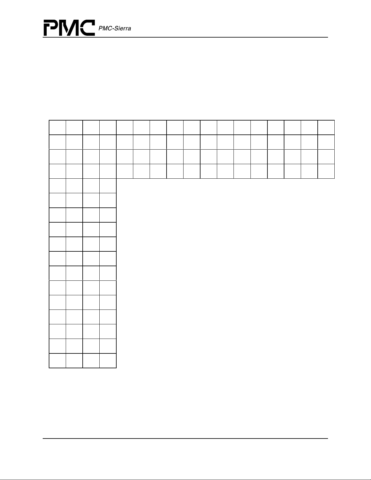
Register 000H: NSE-8G Master Reset..............................................................................58
Register 001H: NSE-8G Individual Channel Reset ...........................................................59
Register 002H: NSE-8G Master JTAG ID .........................................................................60
Register 003H: SBS Page select – Page 0 ....................................................................... 61
Register 004H: SBS Page select – Page 1 ....................................................................... 62
Register 005H: NSE-8G Master Interrupt Source .............................................................63
Register 006H: NSE-8G Master ILC Interrupt Source ......................................................65
Register 007H: NSE-8G Master R8TD Interrupt Source................................................... 66
Register 008H: NSE-8G Master T8TE Interrupt Source ...................................................67
Register 009H: NSE-8G Master Clock Monitor ................................................................. 68
Register 00AH: NSE-8G DCB CMP select........................................................................69
Register 00BH: NSE-8G Interrupt Enable Register ..........................................................70
Register 00CH: NSE-8G Subsystem Interrupt Enable Register ....................................... 71
Register 00DH: NSE-8G R8TD TIP register .....................................................................72
Register 00EH: SBS User Bit 0 ......................................................................................... 73
Register 00FH: SBS User Bit 1 .........................................................................................74
Register 010H: SBS User Bit 2 .........................................................................................75
Register 011H: NSE-8G FREE User Register...................................................................76
Register 012H: Correct R8TD_RX_C1 Pulse Monitor ......................................................77
Register 013H: Unexpected R8TD_RX_C1 Interrupt........................................................ 78
Register 014H: Missing R8TD_RX_C1 Interrupt............................................................... 79
Register 015H: Unexpected R8TD_RX_C1 Interrupt Enable ...........................................80
Register 016H: Missing R8TD_RX_C1 Interrupt Enable ..................................................81
Register 020H, 024H: CSTR #1 – 2 Control* ....................................................................82
Register 021H, 025H: CSTR #1 – 2* Interrupt Enable and CSU Lock Status .................. 83
Register 022H, 026H: CSTR #1 – 2* Interrupt Indication.................................................. 84
Register 044H: DCB Configuration port 11-6 Register......................................................85
Register 045H: DCB Configuration port 5-0 Register .......................................................86
Register 046H: DCB Configuration Output Register. ........................................................87
Register 047H: DCB Access Mode Register .....................................................................88
Register 048H: DCB C1 delay (RC1DLY) register. .......................................................... 91
Register 04AH: DCB Frame size Register ........................................................................92
Register 04CH: DCB Configuration Register ....................................................................93
Proprietary and Confidential to PMC-Sierra, Inc., and for its Customers’ Internal Use 6
Document ID: PMC-2010850, Issue 1
Page 8

NSE-8G™ Standard Product Data Sheet
Preliminary
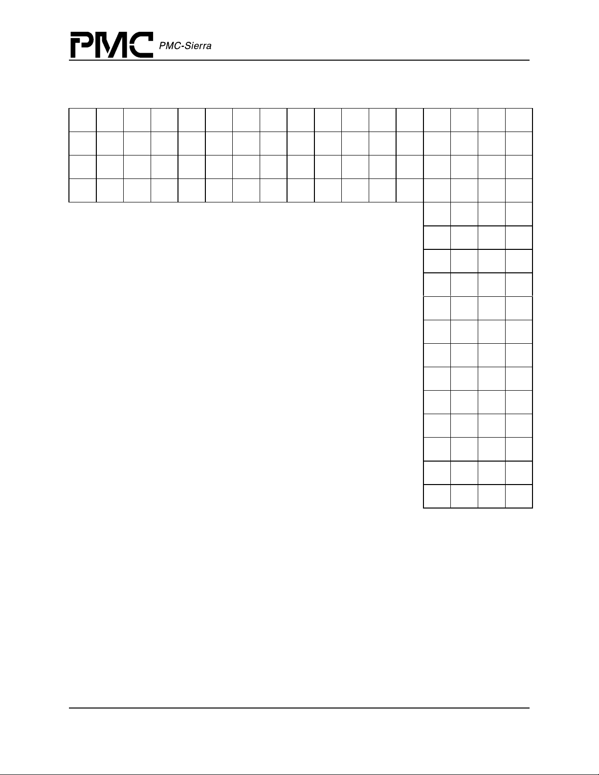
Register 04DH: DCB Interrupt status Register..................................................................96
Register 100H + N*20H, R8TD Control and Status...........................................................97
Register 101H + N*20H, R8TD Interrupt Status................................................................99
Register 102H + N*20H, R8TD Line Code Violation Count ............................................101
Register 103H + N*20H, RXLV and DRU Control ...........................................................102
Register 108H + N*20H, T8TE Control and Status .........................................................104
Register 109H + N*20H, T8TE Interrupt Status ..............................................................106
Register 10AH + N*20H: T8TE Time-slot Configuration #1 ............................................107
Register 10BH + N*20H: T8TE Time-slot Configuration #2 ............................................108
Register 10CH + N*20H, T8TE Test Pattern ...................................................................109
Register 10DH + N*20H, TXLV and PISO Control .......................................................... 110
Register 110H + N*20H, ILC Transmit FIFO Data........................................................... 111
Register 111h + N*20H, ILC Transmit Control Register .................................................112
Register 112h + N*20H, ILC Transmit Misc.Status and FIFO Synch Register................ 113
Register 113h + N*20H, ILC Receive FIFO Data Register.............................................. 115
Register 114h + N*20H, ILC Receive Control Register ................................................... 116
Register 115h + N*20H, ILC Receive Auxiliary, Status and FIFO Synch Register.......... 117
Register 116h + N*20H, ILC Interrupt Enable and Control Register ............................... 121
Register 117h + N*20H: ILC Interrupt Reason Register.................................................. 124
Register 800H: NSE-8G Master Test ..............................................................................126
Proprietary and Confidential to PMC-Sierra, Inc., and for its Customers’ Internal Use 7
Document ID: PMC-2010850, Issue 1
Page 9

NSE-8G™ Standard Product Data Sheet
Preliminary
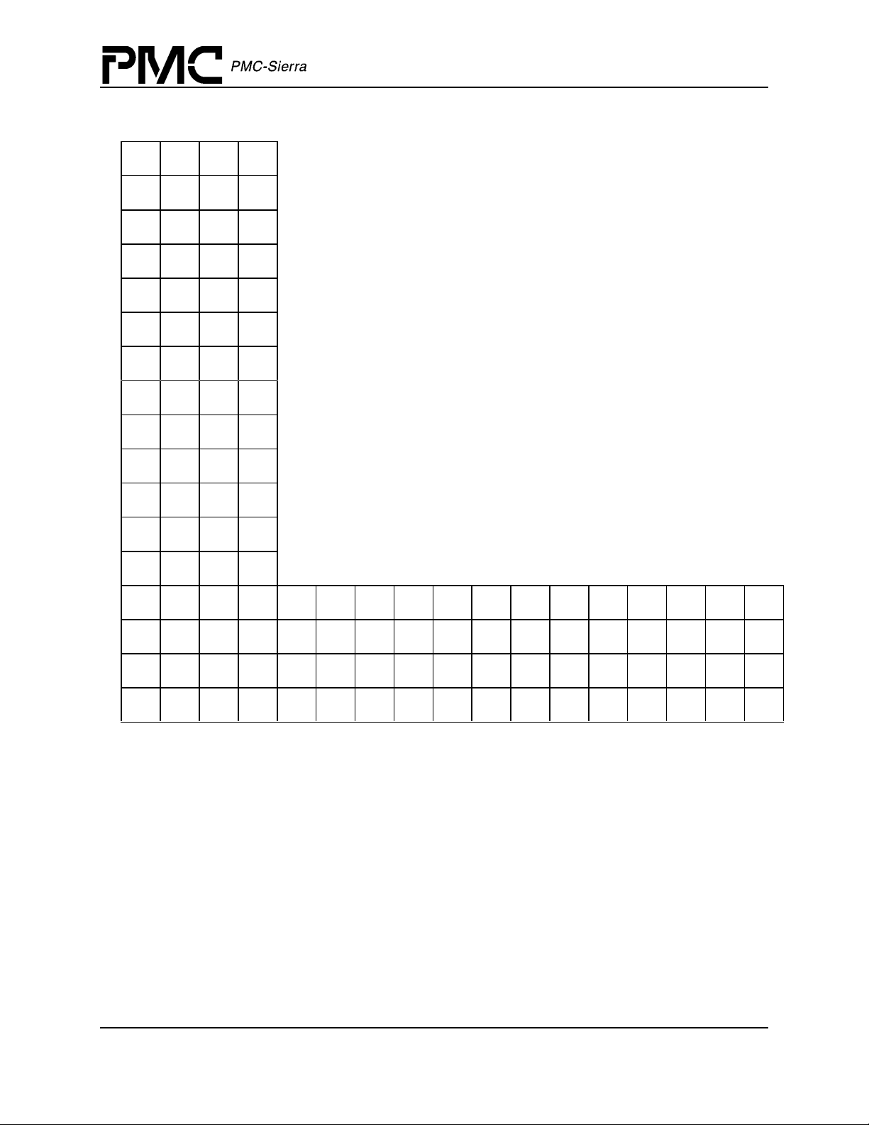
List of Figures
Figure 1 An OC-48 T1/E1 ADM (Individually Drop/Add any T1/E1 in STS-48) ..............14
Figure 2 An OC-48 T1/E1 ADM (Drop/Add up to STS-48 at STS-1 Granularity)............14
Figure 3 Any-Service-Any-Port TDM Access Solution ....................................................15
Figure 4 Any-Service-Any-Port DS0-Granularity PHY Card ...........................................16
Figure 5 NSE- 8G Block Diagram Showing Functional Blocks .......................................17
Figure 6 NSE-8G UBGA-480 Ball Diagram (Bottom-View) .............................................20
Figure 7 Analog Power Filter Circuit................................................................................39
Figure 8 Generic LVDS Link Block Diagram ...................................................................40
Figure 9 Character Alignment State Machine .................................................................47
Figure 10 Frame Alignment State Machine.....................................................................48
Figure 11 In-Band Signaling Channel Message Format ................................................. 52
Figure 12 In-Band Signaling Channel Header Format ....................................................52
Figure 13 Input Observation Cell (IN_CELL) ................................................................131
Figure 14 Output Cell (OUT_CELL) ..............................................................................132
Figure 15 Bidirectional Cell (IO_CELL) .........................................................................132
Figure 16 Layout of Output Enable and Bidirectional Cells...........................................133
Figure 17 Shutting Down a Link ....................................................................................135
Figure 18 “C1” Synchronization Control........................................................................137
Figure 19 TEMUX-84™/SBS/NSE/SBS/AAL1gator-32™ system DS0 Switching
with CAS .......................................................................................................138
Figure 20 CAS Multiframe Timing .................................................................................139
Figure 21 Switch Timing DSOs with CAS .....................................................................139
Figure 22 TEMUX-84/SBS/NSE/SBS/FREEDM-336 System DS0 Switch no
CAS...............................................................................................................140
Figure 23 Switch Timing - DSOs without CAS ..............................................................141
Figure 24 Non DS0 Switch Timing ................................................................................142
Figure 25 Architecture of the RAM Input Interface........................................................144
Figure 26 C1 Position in the First Row..........................................................................149
Figure 27 Transport Overhead Affected by ILC ............................................................155
Figure 28 Example Graph .............................................................................................158
Figure 29 Time:Space:Time Switching in one NSE-8G and four Single-Ported
SBSs .............................................................................................................158
Figure 30 Example Graph .............................................................................................160
Figure 31 Example Problem..........................................................................................161
Proprietary and Confidential to PMC-Sierra, Inc., and for its Customers’ Internal Use 8
Document ID: PMC-2010850, Issue 1
Page 10

NSE-8G™ Standard Product Data Sheet
Preliminary
Figure 32 Merged Graph ...............................................................................................161
Figure 33 Relabeled Graph ...........................................................................................162
Figure 34 Boundary Scan Architecture .........................................................................163
Figure 35 TAP Controller Finite State Machine.............................................................164
Figure 36 Receive Interface Timing ..............................................................................167
Figure 37 Transmit Interface Timing .............................................................................168
Figure 38 CMP Timing ..................................................................................................169
Figure 39 Microprocessor Interface Read Timing .........................................................173
Figure 40 Microprocessor Interface Write Timing .........................................................175
Figure 41 NSE-8G Input Timing ....................................................................................176
Figure 42 RSTB Timing.................................................................................................177
Figure 43 JTAG Port Interface Timing...........................................................................179
Proprietary and Confidential to PMC-Sierra, Inc., and for its Customers’ Internal Use 9
Document ID: PMC-2010850, Issue 1
Page 11

NSE-8G™ Standard Product Data Sheet
Preliminary
List of Tables
Table 1 Analog Power Filters ..........................................................................................39
Table 2 SBI336S Character Encoding ............................................................................43
Table 3 Serial TelecomBus Character Encoding ............................................................45
Table 4 Switching Control RAM Layout...........................................................................50
Table 5 In-band Message Header Fields ........................................................................52
Table 6 NSE-8G Register Map........................................................................................54
Table 7 TX FIFO Message Level ..................................................................................114
Table 8 RX FIFO Message Level ..................................................................................119
Table 9 RXFIFO Threshold Values ...............................................................................122
Table 10 RXFIFO Timeout Delay .................................................................................. 123
Table 11 Test Mode Register Memory Map .................................................................. 125
Table 12 Instruction Register (Length - 3 bits) ..............................................................127
Table 13 Identification Register.....................................................................................127
Table 14 Boundary Scan Register ................................................................................128
Table 15 Absolute Maximum Ratings............................................................................170
Table 16 D.C Characteristics ........................................................................................171
Table 17 Microprocessor Interface Read Access .........................................................173
Table 18 Microprocessor Interface Write Access..........................................................175
Table 19 NSE-8G Input Timing (Figure 40) ..................................................................176
Table 20 RSTB Timing (Figure 41 ) ..............................................................................177
Table 21 Serial SBI Bus Interface ................................................................................. 178
Table 22 JTAG Port Interface ( Figure 42) .................................................................... 178
Proprietary and Confidential to PMC-Sierra, Inc., and for its Customers’ Internal Use 10
Document ID: PMC-2010850, Issue 1
Page 12

1 Features
The Narrowband Switch Element 8G (NSE-8G):
• Implements a Scaleable Bandwidth Interconnect (SBI™) DS0 granularity Space switch.
• Implements a SONET/SDH VT1.5/VT2/TU11/TU12 granularity Space switch for the serial
777.6 MHz LVDS TelecomBus.
• With an allied PM8610 SBS or PM8611 SBS-lite device, implements a DS0 granularity
Memory-Space-Memory switch.
• Supports 12 STS-12 equivalent serial ports via 777.6 MHz, 8B/10B encoded LVDS links
(each port can be either Serial TeleCombus or Serial SBI336S)
• When configured for SBI mode, switches DS0 or N*DS0 for all T1 and E1 tributaries and
aggregate columns for switching T1, E1, TVT1.5, TVT2, DS3 and E3 tributaries.
• When configured for the serial 777.6 MHz TelecomBus interface, switches any SONET/SDH
virtual tributary (VT) or tributary unit (TU) up to STS-1.
NSE-8G™ Standard Product Data Sheet
Preliminary
• Supports switching of arbitrary non-standard octet aggregates.
• Supports unicast, multicast, and broadcast for all switching modes.
• Provides 8 Gbit/s (96,768 DS0s, 4.032 T1s/VT1.5s, 3,024 E1s/VT2s, 144 DS3s/E3s)
switching.
• Works with SBS devices that support up to four 19.44 MHz SBI or one 77.76 MHz SBI336
bus that communicates with PMC-Sierra’s SBI device family. Alternatively, the SBS and
SBS-lite devices support up to four 19.44 MHz STS-3 TelecomBuses or one 77.76 MHz STS12 TelecomBus for connection with PMC-Sierra’s SPECTRA family of devices.
• Can be combined in applications with PMC-Sierra’s CHESS™ chip set devices (PM5374
TSE and PM5307 TBS).
• Supports a microprocessor interface used to configure/control the NSE and make DS0-
granularity switch settings.
• Supports clean error checked 8 Mbit/s full-duplex, in-band communications channels from its
attached microprocessor to the attached microprocessors of each of the 12 attached SBS336S
devices. This channel is used to initialize and control the SBSs, or other such devices, and to
implement call-establishment set-up changes.
• Supports JTAG for all non-LVDS signals.
• Requires dual power supplies at 1.8V and 3.3V.
• Packaged as a 480 ball UBGA.
• In conjunction with the SBS or SBS-lite, supports “1+1” and “1:N” fabric redundancy.
Proprietary and Confidential to PMC-Sierra, Inc., and for its Customers’ Internal Use 11
Document ID: PMC-2010850, Issue 1
Page 13

2 Applications
The PM8621 Narrowband Switch Element 8G (NSE-8G) supports a variety of flexible Layer
1/Layer 2 architectures in combination with the following PMC-Sierra devices:
• PM8610 SBS and PM8611 SBS-lite (SBI Serializer and Memory switching stage).
• SBI bus devices (TEMUX™/TEMAP, FREEDM devices, S/UNI®-IMA devices,
AAL1gator™ devices and other future devices).
• CHESS™ chip set devices (PM5374 TSE, PM5307 TBS, PM5315 SPECTRA™-2488, and
PM7390 S/UNI®-MACH48).
These architectures include:
• T1/E1 SONET ADMs.
• TDM ASAP applications.
• PHY cards with DS0 (and above) level switching.
NSE-8G™ Standard Product Data Sheet
Preliminary
• PSTN replacement switching cores, as part of any-service-any-port applications, and
• Voice Gateways.
Proprietary and Confidential to PMC-Sierra, Inc., and for its Customers’ Internal Use 12
Document ID: PMC-2010850, Issue 1
Page 14

3 References
1. ANSI - T1.105-1995, “Synchronous Optical Network (SONET) – Basic Description
including Multiplex Structure, Rates, and Formats”, 1995.
2. Telcordia - SONET Transport Systems: Common Generic Criteria, GR-253-CORE, Issue 2,
Revision 2, January 1999.
3. ITU, Recommendation G.707 - "Digital Transmission Systems – Terminal equipments -
General", March 1996.
4. IEEE 802.3, “Carrier Sense Multiple Access with Collision Detection (CSMA/CD) Access
Method and Physical Layer Specifications”, Section 36.2, 1998.
5. A.X. Widmer and P.A. Franaszek, “A DC-Balanced, Partitioned-Block, 8B/10B Transmission
Code,” IBM Journal of Research and Development, Vol. 27, No 5, September 1983, pp 440-
451.
NSE-8G™ Standard Product Data Sheet
Preliminary
6. U.S. Patent No. 4,486,739, P.A. Franaszek and A.X. Widmer, “Byte Oriented DC Balanced
(0,4) 8B/10B Partitioned Block Transmission Code,” December 4, 1984.
7. IEEE Std 1596.3-1996, “IEEE Standard for Low-Voltage Differential Signals (LVDS) for
Scalable Coherent Interface (SCI)”, Approved March 21, 1996
8. L.R. Ford, D.R. Fulkerson, “Flows in Networks'', Maximum Cardinality Matchings in
Bipartite Graphs
Proprietary and Confidential to PMC-Sierra, Inc., and for its Customers’ Internal Use 13
Document ID: PMC-2010850, Issue 1
Page 15
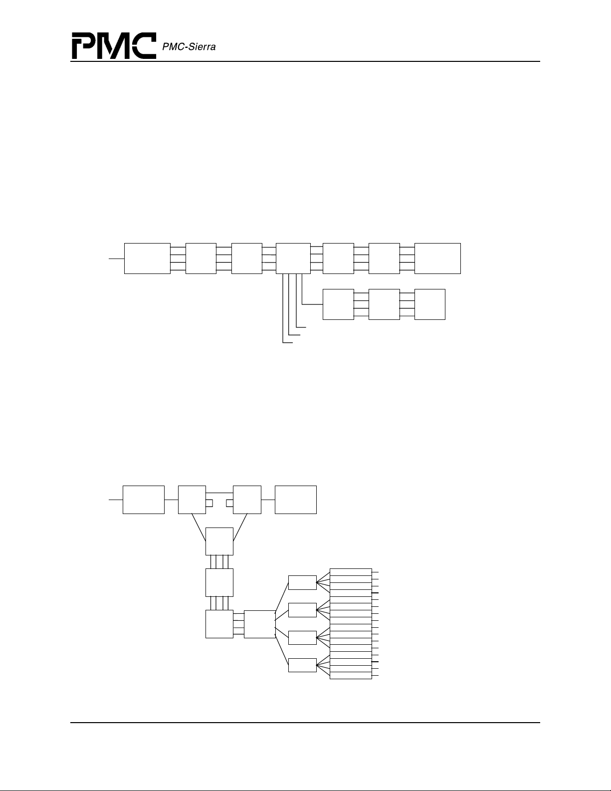
4 Application Examples
Figure 1 illustrates an OC-48 SONET Ring Add/Drop Multiplexer. The PM5363 TUPP-622
devices align all paths to transport frames in preparation for VT1.5/VT2 granularity switching.
The PM8610 SBI336 Bus Serializer (SBS™) an PM8621 Narrowband Switching Element 8G
(NSE-8G™) devices support VT1.5/VT2 and above switching. The Add and Drop buses are
provided by the SBSs that are not in the SONET Ring path. In this case, they connect to T1 and
E1 mapper ports.
Figure 1 An OC-48 T1/E1 ADM (Individually Drop/Add any T1/E1 in STS-48)
NSE-8G™ Standard Product Data Sheet
Preliminary
SPECTRA-
2488
4 X
TUPP-
622
4 X
SBS
NSE20G
4 X
SBS
SBS
**
42 required to terminate
4 X
TUPP-
622
4 X
TEMAP
-84
SPECTRA-
2488
4 X
OCTAL
-LIU **
links for all 4 TEMAPS
Figure 2 illustrates another OC-48 SONET Ring ADM. In this application, the network of three
PM5310 TelecomBus Serializers (TBSs) from PMC-Sierra’s CHESS™ chip set add, drop, and
groom traffic at STS-1 granularities. The four TUPP-622 devices align any dropped STS-1s
(paths to transport frames). The virtual tributary (VT) or tributary unit (TU) switching solution is
provided by the SBS-NSE-8G-SBS network below the TUPP-622s. Four SBSs support up to an
STS-48 amount of add/drop traffic.
Figure 2 An OC-48 T1/E1 ADM (Drop/Add up to STS-48 at STS-1 Granularity)
SPECTA-
2488
TBS TBS
SPECTA-
2488
TBS
4 X
TUPP-
622
4 X
SBS
SBS
SBS
NSE8G
SBS
SBS
SBI device
SBI device
SBI device
SBI device
SBI device
SBI device
SBI device
SBI device
SBI device
SBI device
SBI device
SBI device
SBI device
SBI device
SBI device
SBI device
Proprietary and Confidential to PMC-Sierra, Inc., and for its Customers’ Internal Use 14
Document ID: PMC-2010850, Issue 1
Page 16
NSE-8G™ Standard Product Data Sheet
Preliminary
Figure 3 illustrates the organization of the access line size card(s) from a SONET Any Service
Any Port (ASAP) product. All traffic from the NSE-8G to the SBI link layer devices is pathaligned. See Figure 4 for a description of the PHY line cards compatible with the system in
Figure 3.
Figure 3 Any-Service-Any-Port TDM Access Solution
SBS-
lite
SBS
NSE8G
SBS
SBS
FREEDM-
336
4 X
IMA-84
12 X
AAL1gator-
32
4 X
TEMUX-84
H-MVIP
Any-PHY
(Packet)
Any-PHY
(Cell)
Any-PHY
(Cell)
Processors
DSP
T1/E1/DS0/N*DS0 Layer 2 Processing
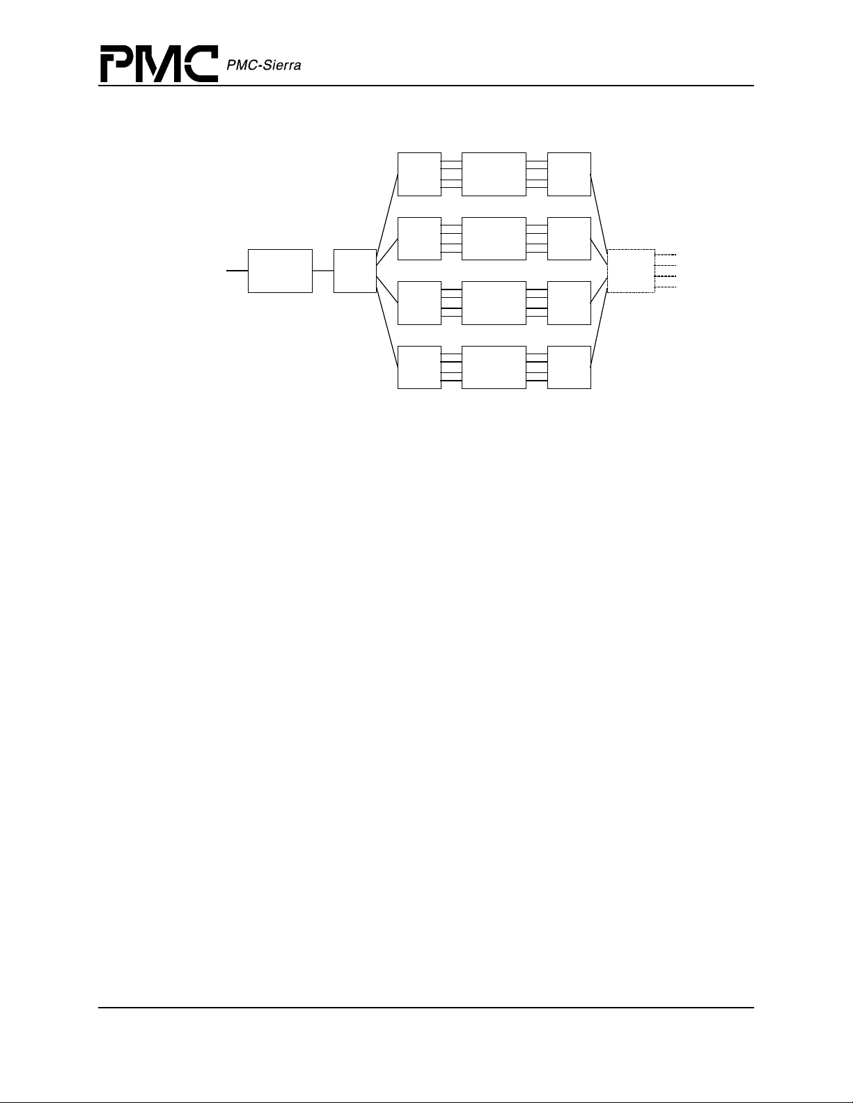
Figure 4 shows the organization of a SONET PHY card compatible with Figure 3. As shown, both
Figure 3 and Figure 4 have NSE-8Gs, but only one instance of this device is required to connect
all the SBSs. A likely packaging of this combined system would place the NSE-8G (and a standby
NSE-8G) on separate fabric cards. In Figure 4, PM8315 TEMUXs align paths to transport frames.
Note: Figure 3 assumes this alignment.
Proprietary and Confidential to PMC-Sierra, Inc., and for its Customers’ Internal Use 15
Document ID: PMC-2010850, Issue 1
Page 17
NSE-8G™ Standard Product Data Sheet
Figure 4 Any-Service-Any-Port DS0-Granularity PHY Card
Preliminary
4 X
TEMUX-84
4 X
TEMUX-84
4 X
TEMUX-84
4 X
TEMUX-84
SPECTRA-
2488
TBS
TBS
TBS
TBS
TBS
SONET/T1/E1 Termination - VT/TU/DS0 Switching
SBS
SBS
NSE8G
SBS
SBS
Proprietary and Confidential to PMC-Sierra, Inc., and for its Customers’ Internal Use 16
Document ID: PMC-2010850, Issue 1
Page 18
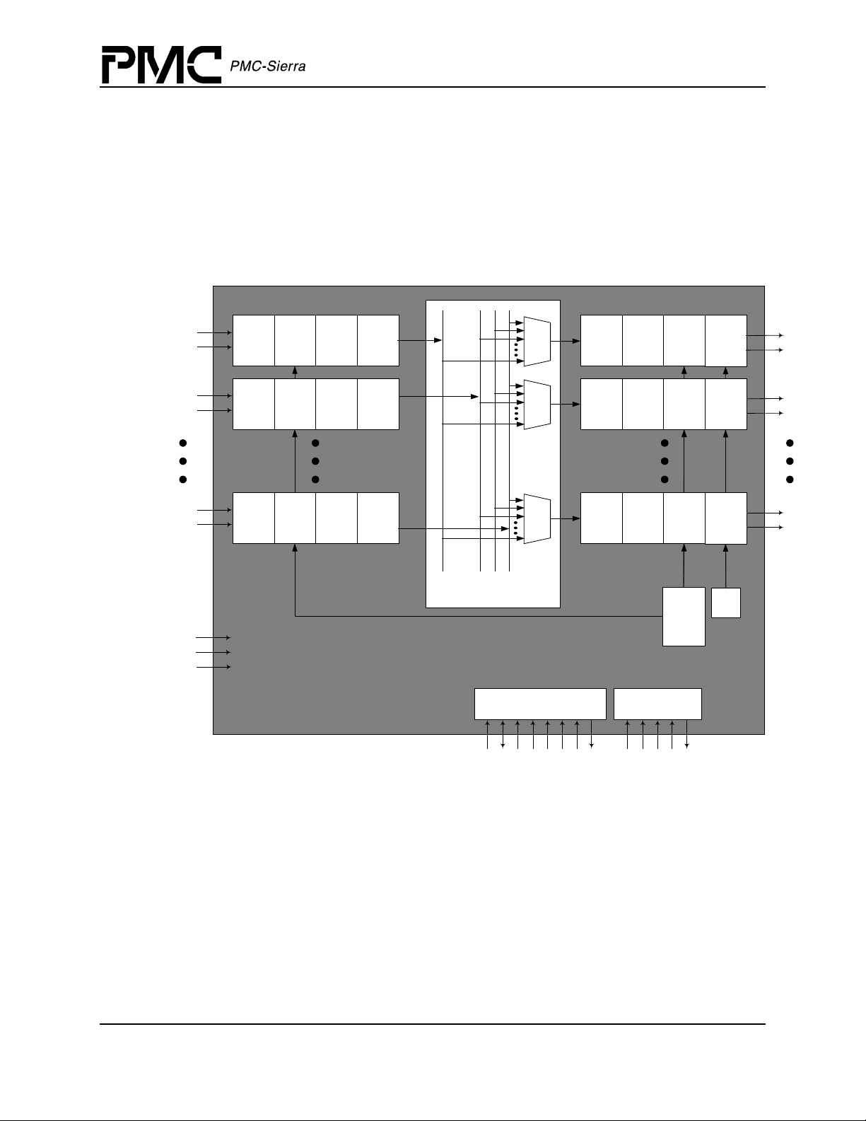
5 Block Diagram
The NSE-8G is organized as a DS0 granularity space switch. Alternatively, the NSE-8G is
organized as a self aligning (with respect to STS-12 boundaries in TelecomBus mode)
VT1.5/VT2 granularity space switch.
Figure 5 NSE- 8G Block Diagram Showing Functional Blocks
NSE-8G™ Standard Product Data Sheet
Preliminary
RP[0]
RN[0]
RP[1]
RN[1]
RP[11]
RN[11]
RC1FP
CMP
SYSCLK
LVDS
Receiver
(RXLV)
LVDS
Receiver
(RXLV)
LVDS
Receiver
(RXLV)
Data
Recovery
Unit
(DRU)
Data
Recovery
Unit
(DRU)
Data
Recovery
Unit
(DRU)
Receive
8B/10B
Decoder
(R8TD)
Receive
8B/10B
Decoder
(R8TD)
Receive
8B/10B
Decoder
(R8TD)
1/2
In-Band
Link
Controller
(ILC)
1/2
In-Band
Link
Controller
(ILC)
1/2
In-Band
Link
Controller
(ILC)
DS0 Crossbar Switch
(DCB)
Microprocessor Interface
1/2
In-Band
Link
Controller
(ILC)
1/2
In-Band
Link
Controller
(ILC)
1/2
In-Band
Link
Controller
(ILC)
Transmit
8B/10B
Encoder
(T8TE)
Transmit
8B/10B
Encoder
(T8TE)
Transmit
8B/10B
Encoder
(T8TE)
JTAG
Transmit
Serializer
(PISO)
Transmit
Serializer
(PISO)
Transmit
Serializer
(PISO)
Clock
Synthesis
Unit
LVDS
Transmitt
er
(TXLV)
LVDS
Transmitt
er
(TXLV)
LVDS
Transmitt
er
(TXLV)
Tx
Ref
TP[0]
TN[0]
TP[1]
TN[1]
TP[11]
TN[11]
CSB
RSTB
A[11:0]
D[31:0]
ALE
RDB
WRB
INTB
TRSTB
TDI
TCK
TMS
TDO
The R8TD, in combination with the RXLV and DRU receive, decode and align incoming
SBI336/STS-12-equivalent LVDS links. Outputs are provided to the primary switching flow and
to the in-band signaling channel. These provide all analog and digital functions to terminate a
full-duplex 777.6 MHz serial SBI336S or 777.6 MHz serial TelecomBus on LVDS.
A 12 X 12 DS0 Crossbar Switch(DCB) stage switches data and control signals between the 12
ports. The switching instructions are stored in two pages of ram configured as offline and online
allowing the user to modify the offline page.
Proprietary and Confidential to PMC-Sierra, Inc., and for its Customers’ Internal Use 17
Document ID: PMC-2010850, Issue 1
Page 19

NSE-8G™ Standard Product Data Sheet
Preliminary
The T8TE, in combination with the PISO and TXLV perform 8B/10B coding and emits the LVDS
bit streams. These provide all analog and digital functions to launch a full-duplex 777.6 MHz
serial SBI336S bus or 777.6 MHz serial TelecomBus on LVDS.
The microprocessor bus interface and in-band signaling units (ILC) provide a clean (error
checked) channel between the NSE-8G and SBSs. This can be used to send messages between the
NSE-8G microprocessor-and the SBS microprocessors in a user defined format.
Proprietary and Confidential to PMC-Sierra, Inc., and for its Customers’ Internal Use 18
Document ID: PMC-2010850, Issue 1
Page 20

6 Description
The PM8621 NSE-8G is a monolithic CMOS integrated circuit packaged in a 480 ball UBGA
that performs DS0 and above granularity space switching on 12 SBI336 streams carried as serial
SBI336S in 8B/10B coding over LVDS at 777.6 Mbit/s. The NSE-8G also performs VT1.5/VT2
and above granularity switching on 12 STS-12/STM-4 SONET/SDH streams, carried as Serial
TelecomBus signals in 8B/10B coding over LVDS at 777.6 Mbit/s.
The NSE-8G is typically used with up to 12 PM8610 SBS or PM8611 SBS-lite devices to provide
Memory-Space-Memory switching systems. As each SBS supports either four SBI buses at 19.44
MHz or one SBI336 bus at 77.76 MHz, the overall system supports any mixture of SBI and
SBI336 byte serial buses, ranging from 48 19.44 MHz SBI buses to 12 SBI336 77.76 MHz buses
that do not exceed an aggregate bandwidth of STS-144, or about 7.5 Gbit/s. In TelecomBus mode,
the SBS devices support the same range of flexibility for 48 19.44 MHz and 12 77.76 MHz
TelecomBuses at VT1.5/VT2 granularity
Central to the NSE-8G is a 12 x 12 cross bar switch. Every clock cycle, the cross bar switches a
byte of data with control signals from each input port to an output port. The byte of data may be a
DS0 channel from a T1/E1 or may be one byte of a column comprising a T1, E1, DS3, E3,
VT1.5, VT2 or STS-1.
NSE-8G™ Standard Product Data Sheet
Preliminary
In order for switching to take place, all input and output streams must be synchronized. This is
done via the RC1FP input signal. When switching T1s, E1s, VTs and other higher order units,
only SBI336 multiframe alignment is required. The same applies for TelecomBus mode where
only frame alignment is required.
An in-band control link over the serial LVDS interface allows the NSE-8G to communicate with
the microprocessors attached to the SBS, SBS-lite or other serial SBI336S devices. The effective
bandwidth of each inband link to each device is 8 Mbit/s. The inband link provides error
detection on 32 byte user messages and some near realtime control signals between devices.
Using the near realtime control signals the NSE-8G is able to synchronize page switching,
indicate switchover between working or protected links and exchange three user defined signals
(software) and eight Auxilliary signals (software). The User and Auxilliary signals can be used to
indicates things like interrupts or can be used for handshaking between the end point
microprocessors. The message format is left to the user of the devices. The only constraint is that
each message is a maximum of 32 bytes long.
Proprietary and Confidential to PMC-Sierra, Inc., and for its Customers’ Internal Use 19
Document ID: PMC-2010850, Issue 1
Page 21
NSE-8G™ Standard Product Data Sheet
Preliminary
7 Pin Diagram
The NSE-8G is packaged in a 35 mm x 35 mm 480 ball UBGA.
Figure 6 NSE-8G UBGA-480 Ball Diagram (Bottom-View)
Upper Left
34 33 32 31 30 29 28 27 26 25 24 23 22 21 20 19 18
A VSS VSS VSS VSS VDDO VSS NC VSS NC VSS
Reserved
VSS
Reserved
VSS
Reserved
VSS VDDI
B VSS AVDH VDDO VDDO VDDO VDDI NC NC NC VDDI
C VSS AVDH AVDH VDDO VDDI
D VSS AVDH AVDH AVDH VDDO
E RESK1 RES1 NC NC
F VSS NC NC AVDL1
GNCNCNCNC
H VSS NC NC AVDH
JNCNCNCNC
K VSS NC NC VDDI
LNCNCNCNC
M VSS NC NC AVDH
N VDDI AVDL2 NC NC
P VSS NC NC VDDI
Reserved
NC NC VDDI NC
Reserved
VDDI VDDO NC NC
Reserved Reserved Reserved Reserved Reserved Reserved
Reserved
Reserved
Reserved Reserved Reserved Reserved
VDDI
Reserved Reserved Reserved
VDDO
VDDO VDDI
RSTB
VDDI
RNCNCNCNC
T NC NC AVDL4 AVDL3
U NC NC AVDL5 CSU_AV
DH
Proprietary and Confidential to PMC-Sierra, Inc., and for its Customers’ Internal Use 20
Document ID: PMC-2010850, Issue 1
Page 22
NSE-8G™ Standard Product Data Sheet
Preliminary
Upper Right
17 16 15 14 13 12 11 10 9 8 7 6 5 4 3 2 1
NC SYSCLK NC VSS NC VSS NC VSS
Reserved
VSS
Reserved
VSS NC VSS VSS VSS VSS A
NC NC NC TCK TMS NC VDDI
Reserved
NC VDDI NC VDDI T DI TDO NC
NC RC1FP VDDI TRSTB VDDI VDDO VDDI CMP
Reserved Reserved Reserved Reserved Reserved
Reserved Reserved Reserved Reserved
Reserved
VDDO
Reserved Reserved
NC VDDO VDDO VDDO VSS B
VDDI VDDO VDDO AVDH VSS C
NC VDDO AVDH AVDH VSS D
AVDH ATB0[1] AVDH AVDH E
ATB1[1] TN[1] TP[1] VSS F
TN[3] TP[3] TN[2] TP[2] G
AVDH VDDI NC VSS H
RP[1] RN[1] TN[4] TP[4] J
VDDI RP[2] RN[2] VSS K
VDDI AVDL14 RP[3] RN[3] L
AVDH RP[4] RN[4] VSS M
TN[6] TP[6] TN[5] TP[5] N
VDDI TN[7] TP[7] VSS P
RP[5] RN[5] TN[8] TP[8] R
AVDH VDDI AVDL13 VSS T
RP[7] RN[7] RP[6] RN[6] U
Proprietary and Confidential to PMC-Sierra, Inc., and for its Customers’ Internal Use 21
Document ID: PMC-2010850, Issue 1
Page 23
Lower Left
VNCNCNCNC
W VSS AVDL6 VDDI AVDH
YNCNCNCNC
AA VSS NC NC VDDI
AB NC NC NC NC
AC VSS NC NC AVDH
AD NC NC AVDL7 VDDI
AE VSS NC NC VDDI
AF NC NC NC NC
AG VSS NC VDDI AVDH
NSE-8G™ Standard Product Data Sheet
Preliminary
AH NC NC NC NC
AJ VSS NC NC ATB1[2]
AK AVDH AVDH ATB0[2] AVDH
AL VSS AVDH AVDH VDDO ALE NC VDDI VDDO A[6] A[2] VDDI VDDO D[27] VDDI NC NC VDDI
AM VSS AVDH VDDO VDDO CSB RDB VDDI A[9] A[5] A[3] D[31] D[29] VDDI D[25] VDDI D[21] D[20]
AN VSS VDDO VDDO VDDO INTB WRB NC A[10] A[7] A[4] A[0] D[30] D[28] D[26] NC D[22] D[19]
AP VSS VSS VSS VSS NC VSS A[11] VSS A[8] VSS A[1] VSS NC VSS D[24] D[23] D[18]
34 33 32 31 30 29 28 27 26 25 24 23 22 21 20 19 18
Proprietary and Confidential to PMC-Sierra, Inc., and for its Customers’ Internal Use 22
Document ID: PMC-2010850, Issue 1
Page 24

Lower Right
NSE-8G™ Standard Product Data Sheet
Preliminary
CSU_AVDHAVDL12 RP[8] RN[8] V
AVDL10 AVDL11 TN[9] T P[9] W
TN[10] TP[10] TN[11] TP[11] Y
VDDI TN[12] TP[12] VSS AA
RP[9] RN[9] AVDL9 VDDI AB
AVDH RP[10] RN[10] VSS AC
RP[11] RN[11] RP[12] RN[12] AD
VDDI NC NC VSS AE
NC NC NC NC AF
AVDH NC NC VSS AG
NC NC NC NC AH
AVDL8 NC NC VSS AJ
NC NC RES2 RESK2 AK
D[17] VDDO D[13] D[11] D[8] VDDO D[5] D[3] D[0] VDDO NC NC VDDO AVDH AVDH AVDH VSS AL
VDDI D[15] VDDI D[10] D[9] D[7] NC D[2] D[1] NC NC NC NC VDDO AVDH AVDH VSS AM
D[16] D[14] D[12] NC VDDI D[6] D[4] VDDI NC NC NC NC VDDO VDDO VDDO AVDH VSS AN
NC VSS VDDI VSS VDDI VSS NC VSS NC VSS NC VSS VDDO VSS VSS VSS VSS AP
17 16 15 14 13 12 11 10 9 8 7 6 5 4 3 2 1
Proprietary and Confidential to PMC-Sierra, Inc., and for its Customers’ Internal Use 23
Document ID: PMC-2010850, Issue 1
Page 25
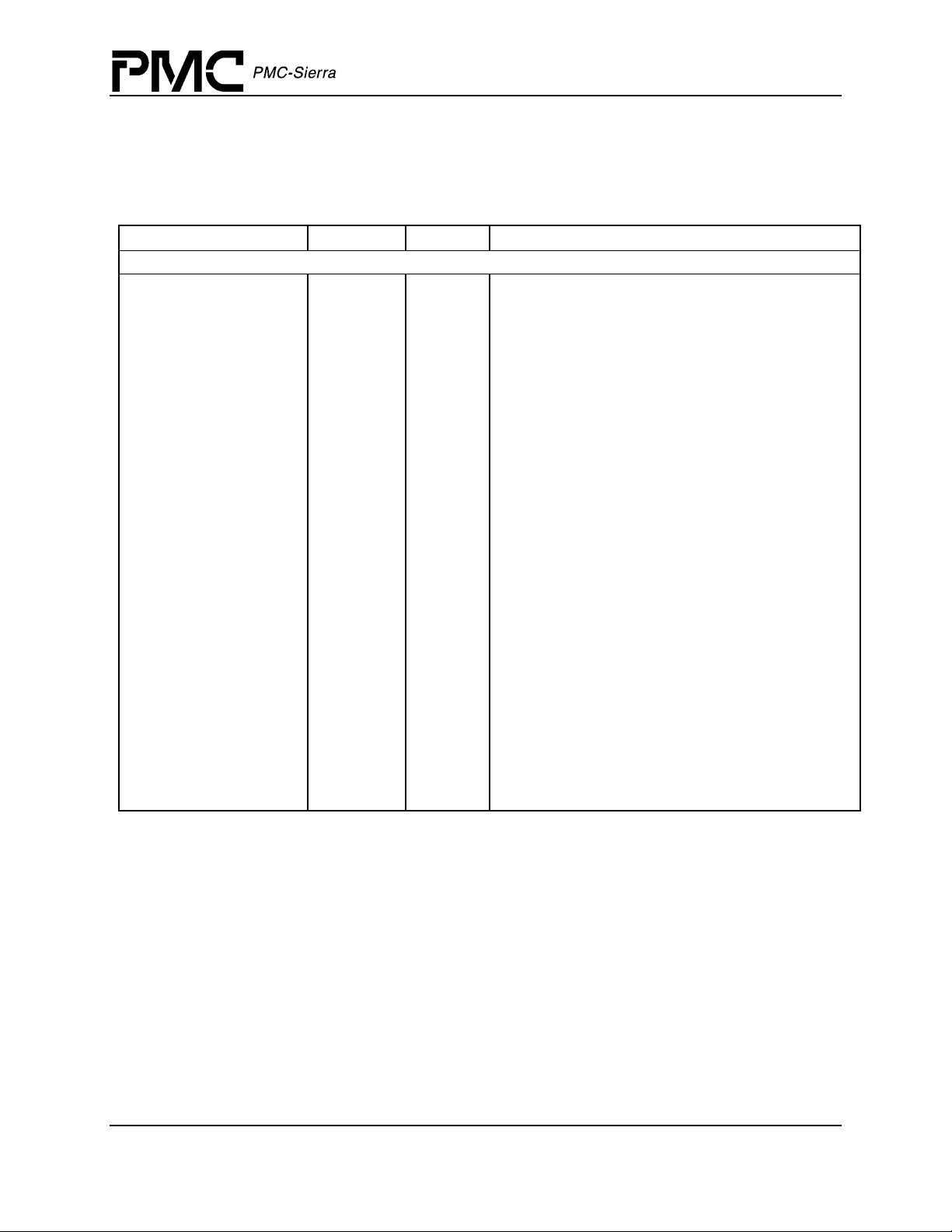
8 Pin Description
8.1 Pin Description Table
Pad Name Type Pin No. Function
LVDS Ports (128 Balls)
RP[1]
RN[1]
RP[2]
RN[2]
RP[3]
RN[3]
RP[4]
RN[4]
RP[5]
RN[5]
RP[6]
RN[6]
RP[7]
RN[7]
RP[8]
RN[8]
RP[9]
RN[9]
RP[10]
RN[10]
RP[11]
RN[11]
RP[12]
RN[12]
Analog
LVDS Input
J4
J3
K3
K2
L2
L1
M3
M2
R4
R3
U2
U1
U4
U3
V2
V1
AB4
AB3
AC3
AC2
AD4
AD3
AD2
AD1
NSE-8G™ Standard Product Data Sheet
Preliminary
Receive Serial Data. The differential receive serial data
links (RP[11:0]/RN[11:0]) carry the receive SBI336S or
SONET/SDH STS-12 frame data from upstream sources
in bit serial format. Each differential pair RP[X]/RN[X]
carries a constituent SBI336 or STS-12 stream. Data on
RP[X]/RN[X] is encoded in an 8B/10B format extended
from IEEE Std. 802.3. The 8B/10B character bit ‘a’ is
transmitted first and the bit ‘j’ is transmitted last. All
RP[X]/RN[X] differential pairs must be frequency locked
and phase aligned (within a certain tolerance) to each
other. RP[11:0]/RN[11:0] are nominally 777.6 Mbit/s data
streams.
Any unused or N/C, but available inputs should be tied
low using a 10 k resistor.
Proprietary and Confidential to PMC-Sierra, Inc., and for its Customers’ Internal Use 24
Document ID: PMC-2010850, Issue 1
Page 26
Pad Name Type Pin No. Function
TP[1]
TN[1]
TP[2]
TN[2]
TP[3]
TN[3]
TP[4]
TN[4]
TP[5]
TN[5]
TP[6]
TN[6]
TP[7]
TN[7]
TP[8]
TN[8]
TP[9]
TN[9]
TP[10]
TN[10]
TP[11]
TN[11]
TP[12]
TN[12]
NSE-8G Control and Clocking (5 Balls)
SYSCLK Input A16
Analog
LVDS
Output
F2
F3
G1
G2
G3
G4
J1
J2
N1
N2
N3
N4
P2
P3
R1
R2
W1
W2
Y3
Y4
Y1
Y2
AA2
AA3
Transmit Serial Data. The differential transmit working
serial data links (TP[11:0]/TN[11:0]) carry the transmit
SBI336S or SONET/SDH STS-12 frame data to a
downstream sinks in bit serial format. Each differential
pair carries a constituent STS-12 stream. Data on
TP[X]/TN[X] is encoded in an 8B/10B format extended
from IEEE Std. 802.3. The 8B/10B character bit ‘a’ is
transmitted first and the bit ‘j’ is transmitted last. All
TP[X]/TN[X] differential pairs are frequency locked and
phase aligned (within a certain tolerance) to each other.
TP[11:0]/TN[11:0] are nominally 777.6 Mbit/s data
streams.
System Clock. The system clock signal (SYSCLK) is the
master clock for the NSE-8G device. SYSCLK must be a
77.76 MHz clock, with a nominal 50% duty cycle.
CMP and RC1FP are sampled on the rising edge of
SYSCLK.
NSE-8G™ Standard Product Data Sheet
Preliminary
Proprietary and Confidential to PMC-Sierra, Inc., and for its Customers’ Internal Use 25
Document ID: PMC-2010850, Issue 1
Page 27
NSE-8G™ Standard Product Data Sheet
Pad Name Type Pin No. Function
RC1FP Input D16
Reserved Output C17 Reserved pin, must be left floating
CMP Input D10
Receive Serial Interface Frame Pulse. The receive
serial interface frame pulse signal (RC1FP) provides
system timing for the receive serial interface. RC1FP is
supplied in common to all devices in a system containing
one or more NSE-20G devices. In TelecomBus mode,
RC1FP is set high once every four frames, in SBI mode
without any DS0 switching, or when switching DS0s
(WITHOUT CAS) RC1FP is also set high once every four
frames, or multiple thereof. When in SBI mode switching
DS0s WITH CAS RC1FP indicates signaling multiframe
alignment by pulsing once every 48 frames or multiples
thereof.
A software configurable delay from RC1FP is used to
indicate that the C1 multiframe boundary 8B/10B
characters have been delivered on all the receive serial
data links (RP[32:1]/RN[32:1]) and are ready for
processing by the time-space-time switching elements.
RC1FP is sampled on the rising edge of SYSCLK.
Connection Memory Page. The connection memory
page select signal (CMP) controls the selection of the
connection memory page in the NSE. When CMP is set
high, connection memory page 1 is selected. When CMP
is set low, connection memory page 0 is selected.
Changes to the connection memory page selection are
synchronized to the boundary of the next C1FP frame or
multiframe depending on the mode:
4-Frame SBI/SBI336 mode:
CMP is sampled at the C1 byte position of the incoming
bus on the first frame of the four-frame multiframe.
Changes to the connection memory page selection are
synchronized to the frame boundary (A1 byte position) of
the next four-frame multiframe.
48-Frame SBI/SBI336 mode:
CMP is sampled at the C1 byte position of the incoming
bus on the first frame of the 48-frame multiframe.
Changes to the connection memory page selection are
synchronized to the frame boundary (A1 byte position) of
the next 48-frame multiframe.
TelecomBus mode:
CMP is sampled at the C1 byte position of every frame
on the incoming bus. Changes to the connection memory
pate selection are synchronized to the frame boundary
(A1 byte position) of the next frame.
Preliminary
CMP is sampled on the rising edge of SYSCLK at the
RC1FP frame position.
RSTB Input B18
Proprietary and Confidential to PMC-Sierra, Inc., and for its Customers’ Internal Use 26
Document ID: PMC-2010850, Issue 1
Reset Enable Bar. The active low reset signal (RSTB)
provides an asynchronous reset for the NSE. RSTB is a
Schmitt triggered input with an integral pull-up resistor
Page 28
Pad Name Type Pin No. Function
Microprocessor Interface (49 Balls)
CSB Input AM30
RDB Input AM29
WRB Input AN29
Chip Select Bar. The active low chip select signal (CSB)
controls microprocessor access to registers in the NSE8G device. CSB is set low during NSE-8G
Microprocessor Interface Port register accesses. CSB is
set high to disable microprocessor accesses.
If CSB is not required (i.e. register accesses controlled
using RDB and WRB signals only), CSB should be
connected to an inverted version of the RSTB input.
Read Enable Bar. The active low read enable bar signal
(RDB) controls microprocessor read accesses to
registers in the NSE-8G device. RDB is set low and CSB
is also set low during NSE-8G Microprocessor Interface
Port register read accesses. The NSE-8G drives the
D[31:0] bus with the contents of the addressed register
while RDB and CSB are low.
Write Enable Bar. The active low write enable bar signal
(WRB) controls microprocessor write accesses to
registers in the NSE-8G device. WRB is set low and CSB
is also set low during NSE-8G Microprocessor Interface
Port register write accesses. The contents of D[31:0] are
clocked into the addressed register on the rising edge of
WRB while CSB is low.
NSE-8G™ Standard Product Data Sheet
Preliminary
Proprietary and Confidential to PMC-Sierra, Inc., and for its Customers’ Internal Use 27
Document ID: PMC-2010850, Issue 1
Page 29
Pad Name Type Pin No. Function
D[31]
D[30]
D[29]
D[28]
D[27]
D[26]
D[25]
D[24]
D[23]
D[22]
D[21]
D[20]
D[19]
D[18]
D[17]
D[16]
D[15]
D[14]
D[13]
D[12]
D[11]
D[10]
D[9]
D[8]
D[7]
D[6]
D[5]
D[4]
D[3]
D[2]
D[1]
D[0]
A[11
A[10]
A[9]
A[8]
A[7]
A[6]
A[5]
A[4]
A[3]
A[2]
A[1]
A{0]
I/O
Input AP28
AM24
AN23
AM23
AN22
AL22
AN21
AM21
AP20
AP19
AN19
AM19
AM18
AN18
AP18
AL17
AN17
AM16
AN16
AL15
AN15
AL14
AM14
AM13
AL13
AM12
AN12
AL11
AN11
AL10
AM10
AM9
AL9
AN27
AM27
AP26
AN26
AL26
AM26
AN25
AM25
AL25
AP24
AN24
Microprocessor Data Bus. The bi-directional data bus,
D[31:0] is used during NSE-8G Microprocessor Interface
Port register reads and write accesses. D[31] is the most
significant bit of the data words and D[0] is the least
significant bit.
Microprocessor Address Bus. The microprocessor
address bus (A[11:0]) selects specific Microprocessor
Interface Port registers during NSE-8G register
accesses.
NSE-8G™ Standard Product Data Sheet
Preliminary
Proprietary and Confidential to PMC-Sierra, Inc., and for its Customers’ Internal Use 28
Document ID: PMC-2010850, Issue 1
Page 30
Pad Name Type Pin No. Function
ALE Input AL30
INTB Open Drain
Output
JTAG Port (5 Balls)
TCK Input B14
TMS Input B13
TDI Input C12
TDO Tri-state C11
TRSTB Input D14
AN30
Address Latch Enable. The address latch enable signal
(ALE) is active high and latches the address bus
(A[11:0]) when it is set low. The internal address latches
are transparent when ALE is set high. ALE allows the
NSE-8G to interface to a multiplexed address/data bus.
ALE has an integral pull up resistor.
Interrupt Request Bar. The active low interrupt enable
signal (INTB) output goes low when an NSE-8G interrupt
source is active and that source is unmasked. INTB
returns high when the interrupt is acknowledged via an
appropriate register access. INTB is an open drain
output.
Test Clock. The JTAG test clock signal (TCK) provides
timing for test operations that are carried out using the
IEEE P1149.1 test access port.
Test Mode Select. The JTAG test mode select signal
(TMS) controls the test operations that are carried out
using the IEEE P1149.1 test access port. TMS is
sampled on the rising edge of TCK. TMS has an integral
pull-up resistor.
Test Data Input. The JTAG test data input signal (TDI)
carries test data into the NSE-8G via the IEEE P1149.1
test access port. TDI is sampled on the rising edge of
TCK. TDI has an integral pull-up resistor.
Test Data Output. TheJTAG test data output signal
(TDO) carries test data out of the NSE-8G via the IEEE
P1149.1 test access port. TDO is updated on the falling
edge of TCK. TDO is a tri-state output which is inactive
except when scanning of data is in progress.
Test Reset Bar. The active low JTAG test reset signal
(TRSTB) provides an asynchronous NSE-8G test access
port reset via the IEEE P1149.1 test access port. TRSTB
is a Schmitt triggered input with an integral pull-up
resistor.
Note that when TRSTB is not being used, it must be
connected to the RSTB input.
NSE-8G™ Standard Product Data Sheet
Preliminary
Proprietary and Confidential to PMC-Sierra, Inc., and for its Customers’ Internal Use 29
Document ID: PMC-2010850, Issue 1
Page 31

Pad Name Type Pin No. Function
Reserved
Reserved Input
External Resistors (4 Balls)
RES[2]
RES[1]
Analog Input AK2
C29
D29
B6
C6
D6
A7
B7
D7
C7
B8
C8
A9
B9
D9
C9
B10
C19
B19
C20
D20
B20
A20
D21
C21
B21
C22
D22
B22
A22
B23
C24
D24
B24
A24
E33
Reserved. Must be left floating [internally pulled up].
Reference Resistor Connection. An off-chip 3.16kΩ
±1% resistor is connected between these the positive
resistor reference pin RES and a Kelvin ground contact
RESK. An on-chip negative feedback path will force the
1.20 V VREF onto RES, therefore forcing 252 µA of
current to flow through the resistor.
NSE-8G™ Standard Product Data Sheet
Preliminary
Proprietary and Confidential to PMC-Sierra, Inc., and for its Customers’ Internal Use 30
Document ID: PMC-2010850, Issue 1
Page 32

Pad Name Type Pin No. Function
RESK[2]
RESK[1]
Analog Test Bus (4 Balls)
ATB0[2]
ATB0[1]
ATB1[2]
ATB1[1]
Digital Core Power (45 Balls)
VDDI[44:0] Power AA4
Analog Input AK1
E34
Analog AK32
E3
Analog AJ31
F4
AB1
AE4
AN10
AN13
AP13
AP15
AM15
AM17
AL18
AM20
AL21
AM22
AL24
AM28
AL28
AG32
AE31
AD31
AA31
W32
P31
N34
K31
T3
P4
Reference Resistor Connection. An off-chip 3.16 kΩ
±1% resistor is connected between these the positive
resistor reference pin RES and a Kelvin ground contact
RESK. An on-chip negative feedback path will force the
1.20 V VREF Voltage onto RES, therefore forcing 252
µA of current to flow through the resistor.
Analog test bus for PMC validation and testing.
This pin must be connected to GND.
Analog test bus for PMC validation and testing.
This pin must be connected to GND.
The digital core power pins (VDDI[44:0]) should be
connected to a well-decoupled +1.8 V DC supply.
NSE-8G™ Standard Product Data Sheet
Preliminary
Proprietary and Confidential to PMC-Sierra, Inc., and for its Customers’ Internal Use 31
Document ID: PMC-2010850, Issue 1
Page 33

Pad Name Type Pin No. Function
VDDI[44:0] Power L4K4
H3
C5
B11
D11
D13C13
C15
D15
C18
D18
A18
C23
B25
C26
D28
B29
C30
Digital I/O Power (34 Balls)
VDDO[33:0] Power AL5
AM4
AN3
AN4
AN5
AP5
AL8
AL12
AL16
AL23
AL27
AL31
AM31
AM32
AN31
AN32
AN33
A30
The digital I/O power pins (VDDO[33:0]) should be
connected to a well-decoupled +3.3 V DC supply.
NSE-8G™ Standard Product Data Sheet
Preliminary
Proprietary and Confidential to PMC-Sierra, Inc., and for its Customers’ Internal Use 32
Document ID: PMC-2010850, Issue 1
Page 34

Pad Name Type Pin No. Function
VDDO[33:0] Power B30
B31
B32
C31
D30
D27
D23
D19
D12
D8
B2
B3
B4
C3
C4
D4
Digital Ground (72 Balls)
VSS [71:0] Ground A1
A2
A3
A4
A6
A8
A10
A12
A14
A19
A21
A23
A25
A27
A29
A31
A32
A33
A34
The digital ground pins (VSS [71:0]) should be
connected to GND.
NSE-8G™ Standard Product Data Sheet
Preliminary
Proprietary and Confidential to PMC-Sierra, Inc., and for its Customers’ Internal Use 33
Document ID: PMC-2010850, Issue 1
Page 35

Pad Name Type Pin No. Function
VSS [71:0] Ground AP1
AP2
AP3
AP4
AP6
AP8
AP10
AP12
AP14
AP16
AP21
AP23
AP25
AP27
AP29
AP31
AP32
AP33
AP34
B1
C1
D1
F1
H1
K1
M1
P1
T1
AA1
AC1
AE1
AG1
AJ1
AL1
AM1
AN1
B34
C34
D34
F34
H34
NSE-8G™ Standard Product Data Sheet
Preliminary
Proprietary and Confidential to PMC-Sierra, Inc., and for its Customers’ Internal Use 34
Document ID: PMC-2010850, Issue 1
Page 36

Pad Name Type Pin No. Function
VSS [71:0] Ground K34
M34
P34
W34
AA34
AC34
AE34
AG34
AJ34
AL34
AM34
AN34
Analog Power (8 Balls)
AVDL[7:0] Power F31
N33
W33
AD32
AJ4
AB2
T2
L3
Clock Synthesis 1.8 V Power (6 Balls)
CSU_AVDL[5:0] Power T31
T32
U32
W4
W3
V3
Clock Synthesis Power (2 Balls)
CSU_AVDH[0:1] Power U31
V4
The analog power pins (AVDL[7:0]) should be connected
to a well-decoupled +1.8 V DC supply. These pins
supply the RXLVs.
The clock synthesis pins (CSU_AVDL[5:0]) should be
connected to a well-decoupled +1.8 V DC supply. These
pins supply the CSUs.
These two pins should be connected to a well-decoupled
+3.3 V DC supply.
NSE-8G™ Standard Product Data Sheet
Preliminary
Proprietary and Confidential to PMC-Sierra, Inc., and for its Customers’ Internal Use 35
Document ID: PMC-2010850, Issue 1
Page 37

Pad Name Type Pin No. Function
Analog I/O Power (34 Balls)
AVDH[33:0] Power H4
M4
T4
AC4
AG4
AL2
AL3
AL4
AM2
AM3
AN2
C2
D2
D3
E1
E2
E4
B33
C32
C33
D31
D32
D33
AG31
AC31
W31
M31
H31
AK31
AK33
AK34
AL32
AL33
AM33
The analog I/O power pins (AVDH[33:0]) should be
connected to a well-decoupled +3.3 V DC supply.
NSE-8G™ Standard Product Data Sheet
Preliminary
Proprietary and Confidential to PMC-Sierra, Inc., and for its Customers’ Internal Use 36
Document ID: PMC-2010850, Issue 1
Page 38

Pad Name Type Pin No. Function
No Connect (50 Balls)
NC[49:0] AG33
AP30
AL29
AN28
AP22
AN20
AL20
AL19
AP17
AN14
AM11
AP11
AN9
AP9
AM8
AN8
AM7
AL7
AN7
AP7
AL6
AM6
AN6
AM5
H2
A5
B5
D5
C10
A11
B12
A13
C14
A15
B15
B16
C16
The No Connect pins (NC[49:0]) should be left floating.
NSE-8G™ Standard Product Data Sheet
Preliminary
Proprietary and Confidential to PMC-Sierra, Inc., and for its Customers’ Internal Use 37
Document ID: PMC-2010850, Issue 1
Page 39

NSE-8G™ Standard Product Data Sheet
Pad Name Type Pin No. Function
NC[49:0] D17
B17
A17
D25
C25
D26
B26
A26
C27
B27
C28
B28
A28
TOTAL 480
Notes
1. All NSE-8G inputs and bi-directional balls except the LVDS links present minimum capacitive loading
and operate at TTL logic levels.
2. Inputs RSTB, ALE, TMS, TDI and TRSTB have internal pull-up resistors.
3. All outputs have a minimum 8 mA drive capability – this includes TDO, INTB and D[31:0]).
4. The VDDI and AVDL power pins are not internally connected to each other. Failure to connect these
pins externally may cause malfunction or damage to the device.
5. The AVDH, CSU_AVDH and VDDO power pins are not internally connected to each other. Failure to
connect these pins externally may cause malfunction or damage to the device.
6. The VDDI, VDDO, AVDH, CSU_AVDH and AVDL power pins all share the common ground VSS.
7. To prevent damage to the device and to ensure proper operation, power must be applied
simultaneously to all 3.3 V power pins followed by power to all the 1.8 V power pins followed by input
pins driven by signals.
8. To prevent damage to the device, power must first be removed from input pins followed by the removal
of power from all the 1.8 V power supply pins followed by the simultaneous removal of power from all
the 3.3 V power pins.
9. The 3.3 V supplies should never be less than the 1.8 V supplies at any time during power-up and
power-down.
Preliminary
8.2 Analog Power Filtering Recommendations
To achieve best performance of the LVDS links, an analog filter network should be installed
between the power balls and the supply.
Proprietary and Confidential to PMC-Sierra, Inc., and for its Customers’ Internal Use 38
Document ID: PMC-2010850, Issue 1
Page 40

NSE-8G™ Standard Product Data Sheet
Table 1 Analog Power Filters
Rs Cl Ch Notes
CSU AVDH (2 balls) 3.3 ohm 100 nF 10 nF One Filter network per VDD ball.
CSU AVDL (6 balls) 0.47 ohm 4.7 µF 10 nF One Filter network per VDD ball.
AVDH (34 balls) 3.3 ohm 1.0 µF 10 nF Two VDD balls per filter network1.
AVDL (8 balls) 0 ohm 100 nF 10 nF One Filter network per VDD ball.
Note
1. Two power-gnd pairs can use the same filter.
Figure 7 Analog Power Filter Circuit
Preliminary
Supply VDD
Supply VSS
Device VDD
R
s
C
l
C
h
Device VSS
Proprietary and Confidential to PMC-Sierra, Inc., and for its Customers’ Internal Use 39
Document ID: PMC-2010850, Issue 1
Page 41

9 Functional Description
9.1 LVDS Overview
The LVDS family of cells allow the implementation of 777.6 Mbit/s LVDS links. A reference
clock of 77.76 MHz is required.
A generic LVDS link according to IEEE 1596.3-1996 is illustrated in Figure 7 below. The
transmitter drives a differential signal through a pair of 50 Ω characteristic interconnects, such as
board traces, backplane traces, or short lengths of cable. The receiver presents a 100 Ω
differential termination impedance to terminate the lines. Included in the standard is sufficient
common-mode range for the receiver to accommodate as much as 925 mV of common-mode
ground difference.
Figure 8 Generic LVDS Link Block Diagram
Transmitter Interconnect Receiver
NSE-8G™ Standard Product Data Sheet
Preliminary
V
op
ΩZo=50
V
ip
100Ω
V
on
V
in
Zo=50Ω
Complete SERDES transceiver functionality is provided. Ten-bit parallel data is sampled by the
line rate divided-by-10 clock (77.76 MHz SYSCLK) and then serialized at the line rate on the
LVDS output pins by a 777.6 MHz clock synthesized from SYSCLK. Serial line rate LVDS data
is sampled and de-serialized to 10-bit parallel data. Parallel output transfers are synchronized to a
gated line rate divided-by-10 clock. The 10-bit data is passed to an 8B/10B decoding block. The
gating duty cycle is adjusted such that the throughput of the parallel interface equals the receive
input data rate (Line Rate +/- 100 ppm). It is expected that the clock source of the transmitter is
the same as the clock source of the receiver to ensure the data throughput at both ends of the link
are identical.
Data is guaranteed to contain sufficient transition density to allow reliable operation of the data
recovery units by 8B/10B block coding and decoding provided by the T8TE and R8TD blocks.
Proprietary and Confidential to PMC-Sierra, Inc., and for its Customers’ Internal Use 40
Document ID: PMC-2010850, Issue 1
Page 42

At the system level, reliable operation will be obtained if proper signal integrity is maintained
through the signal path and the receiver requirements are respected. Namely, a worst case eye
opening of 0.7UI and 100 mV differential amplitude is needed. These conditions should be
achievable with a system architecture consisting of board traces, two sets of backplane
connectors, up to 1m of backplane interconnect. This assumes proper design of 100 Ω differential
lines and minimization of discontinuities in the signal path. Due to power constraints, the output
differential amplitude is approximately 350 mV
The LVDS system is comprised of the LVDS Receiver (RXLV), LVDS Transmitter (TXLV),
Transmitter reference (TXREF), data recovery unit (DRU), parallel to serial converter (PISO and
Clock Synthesis Unit (CSU).
9.1.1 LVDS Receiver (RXLV)
The RXLV block is a 777.6 Mbit/s Low Voltage Differential Signaling (LVDS) Receiver
according to the IEEE 1596.3-1996 LVDS Specification.
The RXLV block is the receiver in Figure 7, accepting 777.6 Mbit/s LVDS signals from the
transmitter, over RP[X]/RN[X] pins, amplifying them and converting them to digital signals, then
passing them to a data recovery unit (DRU). Holding to the IEEE 1596.3-1996 specification, the
RXLV has a differential input sensitivity better than 100 mV, and includes at least 25 mV of
hysteresis. There are 12 RXLV blocks in the NSE.
NSE-8G™ Standard Product Data Sheet
Preliminary
9.1.2 LVDS Transmitter (TXLV)
The TXLV block is a 777.6 Mbit/s Low Voltage Differential Signaling (LVDS) Transmitter
according to the IEEE 1596.3-1996 LVDS Specification.
The TXLV accepts 777.6 Mbit/s differential data from a “parallel-in, serial-out” (PISO) circuit
and then transmits the data off-chip as a LVDS on TP[X]/TN[X] pins.
The TXLV uses a reference current and voltage from the TXREF block to control the output
differential voltage amplitude and the output common-mode voltage.
There are 12 instances of the TXLV block in the NSE-8G.
9.1.3 LVDS Transmit Reference (TXREF)
The TXREF provides an on-chip bandgap voltage reference (1.20 V ±5%) and a precision current
to the TXLV (777.6 Mbit/s LVDS Transmitter) block’s. The reference Voltage is used to control
the common-mode level of the TXLV output, while the reference current is used to control the
output amplitude.
The precision currents are generated by forcing the reference Voltage across an external, off-chip
3.16 kΩ(±1%) resistor. The resulting current is then mirrored through several individual reference
current outputs, so each TXLV receives its own reference current.
There is one instance of the TXREF in the NSE-8G.
Proprietary and Confidential to PMC-Sierra, Inc., and for its Customers’ Internal Use 41
Document ID: PMC-2010850, Issue 1
Page 43

9.1.4 Data Recovery Unit (DRU)
The DRU is a fully integrated data recovery and serial to parallel converter that can be used for
777.6 Mbit/s NRZ data. 8B/10B block code is used to guarantee transition density for optimal
performance.
The DRU recovers data and outputs a ten-bit word synchronized with a line rate divided by ten,
gated clock to allow frequency deviations between the data source and the local oscillator. The
output clock is not a recovered clock. The DRU accumulates 10 data bits and outputs them on the
next clock edge. If 10-bits are not available for transfer at a given clock cycle, the output clock is
gated.
The DRU provides moderate high frequency jitter tolerance suitable for inter-chip serial link
applications. It can support frequency deviations up to ±100 ppm.
There are 12 instances of the DRU on the NSE-8G.
9.1.5 Parallel to Serial Converter (PISO)
The PISO is a parallel-to-serial converter designed for high-speed transmit operation, supporting
up to 777.6 Mbit/s.
NSE-8G™ Standard Product Data Sheet
Preliminary
There are 12 instances of the PISO on the NSE-8G.
9.1.6 Clock Synthesis Unit (CSU)
The CSU is a fully integrated clock synthesis unit. It generates low jitter multi-phase differential
clocks at 777.6 MHz for the use by the transmitter.
There is one instance of the CSU on the NSE-8G.
9.2 Receive 8B/10B Frame Aligner (R8TD)
The Receive 8B/10B serial SBI336S Bus frame aligner, R8TD, frames to the receive stream to
find 8B/10B character boundaries. It also contains a FIFO to bridge between the timing domain of
the receive LVDS links and the system clock timing domain. The R8TD blocks perform framing
and elastic store functions on data retrieved from the receive LVDS links, RP[x]/RN[x].
9.2.1 FIFO Buffer
The FIFO buffer sub-block provides isolation between the timing domains of the associated
receive LVDS link and that of the system clock, SYSCLK. Data with arbitrary alignment to the
8B/10B characters, are written into a 10-bit by 24-word deep FIFO at the link clock rate. Data is
read from the FIFO at every SYSCLK cycle.
Proprietary and Confidential to PMC-Sierra, Inc., and for its Customers’ Internal Use 42
Document ID: PMC-2010850, Issue 1
Page 44

9.3 Transmit 8B/10B Encoder (T8TE)
The Transmit 8B/10B Encoder blocks, T8TE, construct an 8B/10B character stream from an
incoming translated SBI336 or TelecomBus carrying an STS-12/STM-4 equivalent channelized
stream. The T8TE block corrects the running disparity of an 8B/10B character stream and buffers
data in a FIFO before transmission to the transmit serializer block. A total of 32 T8TE blocks are
instantiated in the NSE-20G device.
In SBI mode, these blocks encode the SBI336S stream as shown in Table 2. When configured for
Synchronous mode for DS0 switching, the 8B/10B encoder transmits CAS signaling multiframe
alignment across the SBI336S interface by generating a C1FP character every 48 frame times.
When not configured for DS0 switching, the C1FP character is sent every four frames.
9.3.1 SBI336S 8B/10B Character Encoding
Table 2 shows the mapping of SBI336S bus control bytes and signals into 8B/10B control
characters. The linkrate octet in location V4, V1 and V2, the in-band programming channel, the
V3 octet when it contains data are all carried as data. Justification requests for master timing are
carried in the V5 character so there are three V5 characters used, nominal, negative timing
adjustment request, positive timing adjustment request.
NSE-8G™ Standard Product Data Sheet
Preliminary
Table 2 SBI336S Character Encoding
Code Group
Name
Common to All Link Types
K28.5 001111 1010 110000 0101 IC1FP=’b1
K23.7- 111010 1000 - Overhead Bytes (columns 1-60 or 1-72
Asynchronous T1/E1 Links
K27.7- 110110 1000 - V5 byte, no justification request
K28.7- 001111 1000 - V5 byte, negative justification request
K29.7- 101110 1000 - V5 byte, positive justification request
Synchronous T1/E1 Links
K27.7- 110110 1000 - V5 byte
Asynchronous DS3/E3 Links
K27.7- 110110 1000 - V5 byte, no justification request
K28.7- 001111 1000 - V5 byte, negative justification request*
K29.7- 101110 1000 - V5 byte, positive justification request*
Fractional Rate Links
K28.7- 001111 1000 - V5 byte, send one extra byte request**
Curr. RDabcdei fghj
Curr. RD+
abcdei fghj
Encoded Signals
Description
C1FP frame and multiframe alignment
except for C1 and in-band programming
channel), V3 or H3 byte except during
negative justification, byte after V3 or H3
byte during positive justification, unused
bytes in fraction rate links
Proprietary and Confidential to PMC-Sierra, Inc., and for its Customers’ Internal Use 43
Document ID: PMC-2010850, Issue 1
Page 45

NSE-8G™ Standard Product Data Sheet
Preliminary
Code Group
Name
K29.7- 101110 1000 - V5 byte, send one less byte request**
Floating Transparent Virtual Tributaries
K27.7- 110110 1000 - V5 byte
K27.7+ - 001001 0111
K28.7- 001111 1000 - V5 byte
K28.7+ - 110000 0111 V5 byte
K29.7- 101110 1000 - V5 byte
K29.7+ - 010001 0111 V5 byte
K30.7- 011110 1000 - V5 byte
K30.7+ - 100001 0111 V5 byte
Curr. RDabcdei fghj
Curr. RD+
abcdei fghj
Encoded Signals
Description
IV5=1,
IDATA[0,4] = ERDI[1:0] = ‘b00, IDATA[5] =
REI = ‘b0
V5 byte
IV5=1,
IDATA[0,4] = ERDI[1:0] = ‘b00, IDATA[5] =
REI = ‘b1
IV5=1,
IDATA[0,4] = ERDI[1:0] = ‘b01, IDATA[5] =
REI = ‘b0
IV5=1,
IDATA[0,4] = ERDI[1:0] = ‘b01, IDATA[5] =
REI = ‘b1
IV5=1,
IDATA[0,4] = ERDI[1:0] = ‘b10, IDATA[5] =
REI = ‘b0
IV5=1,
IDATA[0,4] = ERDI[1:0] = ‘b10, IDATA[5] =
REI = ‘b1
IV5=1,
IDATA[0,4] = ERDI[1:0] = ‘b11, IDATA[5] =
REI = ‘b0
IV5=1,
IDATA[0,4] = ERDI[1:0] = ‘b11, IDATA[5] =
REI = ‘b1
* Note there can be multiple V5s per SBI frame when in DS3 or E3 mode but only one
justification can occur per SBI frame. Positive and negative justification request through V5
required by the SBI336S interface should be limited to one per frame.
** Note fractional rate links are symmetric in the transmit and receive direction over SBI336S.
When using clock slave mode with a fractional rate link the clock master makes single byte
adjustments to the slaves rate once per frame.
9.3.2 Serial TelecomBus 8B/10B Character Encoding
Table 3 shows the mapping of TelecomBus control bytes and signals into 8B/10B control
characters. When the TelecomBus control signals conflict each other, the 8B/10B control
characters are generated according to the sequence of the table, with the characters at the top of
the table taking precedence over those lower in the table.
Proprietary and Confidential to PMC-Sierra, Inc., and for its Customers’ Internal Use 44
Document ID: PMC-2010850, Issue 1
Page 46

Table 3 Serial TelecomBus Character Encoding
NSE-8G™ Standard Product Data Sheet
Preliminary
Code Group
Name
High Order Path Termination (HPT) Mode
K28.5 001111 1010 110000 0101 IC1FP=’b1
K28.0- 001111 0100 - IPL=’b0
K28.0+ - 110000 1011 IPL=’b0
K28.6 001111 0110 110000 1001
Low Order Path Termination (LPT) Mode
K28.4+ - 110000 1101 ITAIS=’b1
K27.7- 110110 1000 - IV5=’b1,
K27.7+ - 001001 0111 IV5=’b1,
K28.7- 001111 1000 -
K28.7+ - 110000 0111
K29.7- 101110 1000 -
K29.7+ - 010001 0111
Curr. RDabcdei fghj
Curr. RD+
abcdei fghj
Encoded Signals
Description
IPL=’b0
C1FP frame and multiframe alignment
High-order path H3 byte position, no
negative justification event.
High-order path PSO byte position, positive
justification event.
IC1FP=’b1,
IPL=’b1
High-order path frame alignment (J1).
Low-order path AIS.
IDATA[0,4] = ERDI[1:0] = ‘b00, IDATA[5] =
REI = ‘b0
Low order path frame alignment. ERDI and
REI are encoded in the V5 byte.
IDATA[0,4] = ERDI[1:0] = ‘b00, IDATA[5] =
REI = ‘b1
Low order path frame alignment. ERDI and
REI are encoded in the V5 byte.
IV5=’b1,
IDATA[0,4] = ERDI[1:0] = ‘b01, IDATA[5] =
REI = ‘b0
Low order path frame alignment. ERDI and
REI are encoded in the V5 byte.
IV5=’b1,
IDATA[0,4] = ERDI[1:0] = ‘b01, IDATA[5] =
REI = ‘b1
Low order path frame alignment. ERDI and
REI are encoded in the V5 byte.
IV5=’b1,
IDATA[0,4] = ERDI[1:0] = ‘b10, IDATA[5] =
REI = ‘b0
Low order path frame alignment. ERDI and
REI are encoded in the V5 byte.
IV5=’b1,
IDATA[0,4] = ERDI[1:0] = ‘b10, IDATA[5] =
REI = ‘b1
Low order path frame alignment. ERDI and
Proprietary and Confidential to PMC-Sierra, Inc., and for its Customers’ Internal Use 45
Document ID: PMC-2010850, Issue 1
Page 47

K30.7- 011110 1000 - IV5=’b1,
K30.7+ - 100001 0111
K23.7- 111010 1000 000101 0111 ITPL=’b0
9.3.3 Serial SBI336S and TelecomBus Alignment
The alignment functionality preformed by each receiver can be broken down into two parts,
character alignment and frame alignment. Character alignment finds the 8B/10B character
boundary in the arbitrarily aligned incoming data. Frame alignment finds SBI336S or
TelecomBus frame and multiframe boundaries within the Serial link.
NSE-8G™ Standard Product Data Sheet
Preliminary
REI are encoded in the V5 byte.
IDATA[0,4] = ERDI[1:0] = ‘b11, IDATA[5] =
REI = ‘b0
Low order path frame alignment. ERDI and
REI are encoded in the V5 byte.
IV5=’b1,
IDATA[0,4] = ERDI[1:0] = ‘b11, IDATA[5] =
REI = ‘b1
Low order path frame alignment. ERDI and
REI are encoded in the V5 byte.
Non low-order path payload bytes.
The character and frame alignment are expected to be robust enough for operation over a cabled
interconnect.
9.3.4 Character Alignment Block
Character alignment locates character boundaries in the incoming 8B/10B data stream. The
character alignment algorithm may be in one of two states, in-character-alignment state and outof-character-alignment state. The two states of the character alignment algorithm is shown in
Figure 8.
When the character alignment state machine is in the out-of-character-alignment state, it
maintains the current alignment, while searching for a C1FP character. If it finds the C1FP
character, it will re-align to the C1FP character and move to the in-character-alignment state. The
C1FP character is found by searching for the 8B/10B C1FP character, K28.5+ or K28.5-,
simultaneously in ten possible bit locations. While in the in-character-alignment state, the state
machine monitors LCVs. If 5 or more LCVs are detected within a 15 character window the
character alignment state machine transitions to out-of-character-alignment state. The special
characters listed in Table 2 and Table 3 are ignored for LCV purposes. Upon return to incharacter-alignment state the LCV count is cleared.
Proprietary and Confidential to PMC-Sierra, Inc., and for its Customers’ Internal Use 46
Document ID: PMC-2010850, Issue 1
Page 48

Figure 9 Character Alignment State Machine
5-in-15 LCVs
NSE-8G™ Standard Product Data Sheet
Preliminary
out-of-
character-
alignment
9.3.5 Frame Alignment
Frame alignment locates SBI or TelecomBus frame and multiframe boundaries in the incoming
8B/10B data stream. The frame alignment state machine may be in one of two states, in-framealignment state and out-of-frame-alignment state. Each SBI336S frame is 125 µS in duration.
In SBI mode: Encoded over the SBI336S frame alignment is SBI336S multiframe alignment
which is every four SBI336S frames or 500 µS. When carrying DS0 traffic in synchronous mode,
signaling multiframe alignment is also necessary and is also encoded over SBI336S alignment.
Signaling multiframe alignment is every 24 frames for T1 links and every 16 frames for E1 links,
therefore signaling multiframe alignment covering both T1 and E1 multiframe alignment is every
48 SBI336S frames or 6ms. Therefore C1FP characters are sent every four or every 48 frames.
in-
character-
alignment
Found C1FP Character
In TelecomBus mode: Encoded over the serial link is the tributary multiframe alignment which is
every 4 frames or 500 µS. Multiframe alignment is required so that a downstream device can
extract the T1 or E1 data from the tributary. The multiframe information is preserved by only
sending out C1FP characters every four frames.
Proprietary and Confidential to PMC-Sierra, Inc., and for its Customers’ Internal Use 47
Document ID: PMC-2010850, Issue 1
Page 49

NSE-8G™ Standard Product Data Sheet
Preliminary
The frame alignment state machine establishes frame alignment over the link and is based on the
frame and not the multiframe alignments. When the frame alignment state machine is in the outof-frame-alignment state, it maintains the current alignment, while searching for a C1FP
character. When it finds the C1FP character the state machine transitions to the in-framealignment state. While in the in-frame-alignment state, the state machine monitors out-of-place
C1FP characters. Out-of-place C1FP characters are identified by maintaining a frame counter
based on the C1FP character. The counter is initialized by the C1FP character when in the out-ofcharacter-alignment state, and is unaffected in the in-character-alignment state. If three
consecutive C1FPs have been found that do not agree with the expected location as defined by the
frame counter, the state will change to out-of-frame-alignment state.
The frame alignment state machine is also sensitive to character alignment. When the character
alignment state machine is in the out-of-character-alignment state, the frame alignment state
machine is forced out-of-alignment, and is held in that state until the character alignment state
machine transitions to the in-character alignment state.
Figure 10 Frame Alignment State Machine
out-offrame-
alignment
3 consecutive out-of-place
C1FPs or
out-of-character alignment
in-frame-
alignment
Found C1FP and
not (out-of-character alignment)
Proprietary and Confidential to PMC-Sierra, Inc., and for its Customers’ Internal Use 48
Document ID: PMC-2010850, Issue 1
Page 50

9.3.6 SBI336S Multiframe Alignment
SBI336S multiframe alignment is communicated across the link by controlling the frequency of
the C1FP character. The most frequent transmission of the C1FP character is every four SBI336S
frame times. This is the SBI336S multiframe and is used when there are no synchronous
tributaries requiring signalling multiframe alignment on the SBI336S bus. When there are
synchronous tributaries on the SBI336S bus the C1FP character is transmitted every 48 frame
times. This is the CAS signaling multiframe and is the lowest common multiple of the 24 frame
T1 multiframe and the 16 frame E1 multiframe.
The SBI336S multiframe and signaling multiframe alignment is based a free running multiframe
counter that is reset with each C1FP character received. Under normal operating conditions each
received C1FP character will coincide with the free running multiframe counter. SBI336S
multiframe alignment is always required, SBI336S signaling multiframe alignment is optional
and only required when synchronous tributaries are supported with DS0 level switching.
9.4 DS0 Cross Bar switch (DCB)
Each of 12 R8TD blocks provides an eight-bit data signal on each 77.76 MHz clock edge. These
signals are the STS-12 frame aligned ingress octets. Likewise, each of 12 egress T8TE blocks
expects to receive a STS-12 frame aligned signal on each clock edge. The DS0 Cross Bar switch
(DCB) connects these inputs to these outputs.
NSE-8G™ Standard Product Data Sheet
Preliminary
The DCB constitutes a Space switch that connects each output to some input during each clock
period in the STS-12 frame structure. The STS-12 frame structure consists of 12*9*90 = 9720
octets (of overheads and payload). Being a DS0 granularity space switch, the DCB must provide
separate switch settings for each of these 9720 octet times.
These 9720 switch settings are stored in an on-chip SRAM. Each of twelve egress ports must be
told which of each of twelve ingress ports it should read during each of the 9720 clock periods.
Five bits are required to specify which ingress port should be read by each output. Thus, we
require 9720 words of five bits each for twelve egress ports. Thus each clock period requires 12
*5 = 60 bits. To support controlled switchover from one set of switch settings to another, we
require two banks of 9720 words each. The aggregate memory requirement is 2 X 9720 X 60b =
1,166,400b of SRAM. Table 4 illustrates the mapping of this memory. Each control page in the
table is a vector of 60 bits containing five bits (specifying the source port) for each of 12 egress
ports. One page will be on-line translating ports in the core switch while the other is offline for
CPU update. When the new configuration is ready, and the appropriate system synchronized
frame boundary arrives, the pages will be swapped.
Proprietary and Confidential to PMC-Sierra, Inc., and for its Customers’ Internal Use 49
Document ID: PMC-2010850, Issue 1
Page 51

NSE-8G™ Standard Product Data Sheet
Preliminary
Table 4 Switching Control RAM Layout
Control Page 0 Control Page 1
RAM Address STS Row Col STS Row
0111111
1211211
……
9719 12 9 90 12 9 90
Col
The multiplexers that select the inputs for each egress port are straight forward 12 to-1
multiplexers. They require five bits of control during each 77.76 MHz clock cycle. Their outputs
go to the T8TEs. This design permits unicast, multicast, and broadcast.
9.5 Clock Synthesis and Transmit Reference Digital Wrapper (CSTR)
The CSTR contains the configuration registers for the CSU and TXREF LVDS analog locks.
9.6 Fabric Latency
The flow of octets from ingress LVDS to egress LVDS has variable latency, depending on the
timing of the arriving LVDS stream, and the clock variation on the egress LVDS drivers. A
reasonable estimate of the NSE’s latency can be arrived at by making assumptions about the
depths of the receive and transmit FIFOs: we assume the “C1” timing is set to maintain about
four samples in the ingress FIFO; the egress FIFO is designed to be centered at four samples – so
typically delay due to FIFOs will be 8 clock cycles. The latency through the space switch stage is
three clock cycles. Data latency through the analog blocks is around 90 ns. The typical latency of
the NSE-8 G is 24 clock cycles or 308 ns. With worst case conditions in both FIFOs, latency rises
to 36 clock cycles or 463 ns.
9.7 JTAG Support
The NSE-8G provides JTAG support for testing device interconnection on a PC board.
9.8 Microprocessor Interface
The Microprocessor Interface Block provides the logic required to interface the normal mode and
test mode registers within the NSE-8G to a generic microprocessor bus. The normal mode
registers are used during normal operation to configure and monitor the NSE. The register set is
accessed as shown in the Register Memory Map table below. Addresses that are not shown are
not used and must be treated as Reserved.
Proprietary and Confidential to PMC-Sierra, Inc., and for its Customers’ Internal Use 50
Document ID: PMC-2010850, Issue 1
Page 52

9.9 In-band Link Controller (ILC)
In order to permit centralized control of distributed NSE/SBS fabrics from the NSE-8G
microprocessor interface (for applications in which NSEs are located on fabric cards, and SBSs
are located on multiple line cards), an in-band signaling channel is provided between the NSE-8G
and the SBS over the Serial SBI336S interface. Each NSE-8G can control up to 12 SBSs that are
attached by the LVDS links. The NSE-SBS in-band channel is full duplex, but the NSE-8G has
active control of the link.
The in-band channel is carried in the first 36 columns of four rows of the SBI structure, rows 3, 6,
7 and 8. The overall in-band channel capacity is thus 36*4*64 kb/s = 9.216 Mbit/s. Each 36 bytes
per row allocated to the in-band signaling channel is its own in-band message between the end
points. Four bytes of each 36 byte inband message are reserved for end-to-end control
information and error protection, leaving 8.192 Mbit/s available for data transfer between the end
points.
The data transferred between the end points has no fixed format, effectively providing a clear
channel for packet transfer between the attached microprocessors at each of the LVDS link
terminating devices. The user is able to send and receive any packet up to 32 bytes in length. The
last two reserved bytes of the 36 byte in-band message is a CRC-16 which detects errors in the
message. This block provides a microprocessor interface to the in-band signaling channel.
NSE-8G™ Standard Product Data Sheet
Preliminary
This in-band channel is expected to be used almost entirely to carry out switching control changes
in the SBSs. To configure a DS0 in an SBS device most often requires a local microprocessor to
write to one memory location consisting of a 16-bit address and a 16-bit data. Using this as a
baseline and assuming an efficient use of the in-band channel bandwidth, we can set a maximum
of (32bytes/row * 4 rows/frame * 8000 frames/sec / 4 bytes/write) 256,000 DS0 configurations
per second.
Considering that configuring a T1 when switching DS0s requires 27 DS0 writes, indicates that
the in-band signaling channel bandwidth sets maximum limit of over 9000 T1 configurations per
second. In real life these limits will not be achieved but this shows that the in-band link should
not be the bottleneck. In TelecomBus mode, this same configuration will require only three writes
per T1 link. Another more efficient communication scheme could be used to increase this
performance.
In N+1 protected architectures, it is likely that full configuration of a port card will be necessary
during the switchover. This would require the entire connection memory be reconfigured.
Assuming connections for overhead bytes are also reconfigured, the fastest that a complete
reconfiguration can take place is 9720 register writes for each of the two configuration pages in
the SBS. This equates to (2 * 9720 writes * 4 bytes/write / (32 bytes/row * 4 rows/frame * 8000
frames/second)) 76 milliseconds. It is also possible that the spare card could hold all the
connection configurations for all the port cards it is protecting locally, for even faster switch over.
Proprietary and Confidential to PMC-Sierra, Inc., and for its Customers’ Internal Use 51
Document ID: PMC-2010850, Issue 1
Page 53

9.9.1 In-Band Signaling Channel Fixed Overhead
The In-Band Link Controller block generates and terminates two bytes of fixed header and a
CRC-16 per every 32 byte in-band message (total 36 bytes). The two byte header provides control
and status between devices at the ends of the LVDS link. The CRC-16 is calculated over the 32
byte (and header - 34 bytes) in-band message and provides the terminating end the ability to
detect errors in the in-band message. The format of the in-band message and header bytes is
shown in Figure 11 and Figure 12.
Figure 11 In-Band Signaling Channel Message Format
1 byte 1 byte 32 bytes 2 bytes
Header1 Header2 Free Format Information CRC-16
Figure 12 In-Band Signaling Channel Header Format
Header1
Bit 7 Bit 6 Bit 5 Bit4 Bit3 Bit2 Bit1 Bit 0
VALID LINK[1:0] PAGE[1:0] USER[2:0]
NSE-8G™ Standard Product Data Sheet
Preliminary
Header2
Bit 7 Bit 6 Bit 5 Bit4 Bit3 Bit2 Bit1 Bit 0
AUX[7:0]
Table 5 In-band Message Header Fields
Field Name NSE-8G to SBS SBS to NSE
Valid Message slot contains a message(1)
or is empty(0). If empty this message
will not be put into Rx Message FIFO
(other header information processed
as usual)
Link[1:0]# These bits are optional for SBI336S
devices, intended for devices which
have multiple redundant links. Each
bit either indicates which Link to use,
Working(0) or Protect(1) when
sourced from the master device, or
which link is being used, when
sourced from the slave device. Other
algorithms are possible to indicate
Working or Protect over these 2 bits
but all SBI336S devices must be able
to revert back to this meaning.
Transmitted immediately.
Message slot contains a message(1)
or is empty(0). If empty this message
will not be put into Rx Message FIFO
(other header information processed
as usual)
These bits are optional for SBI336S
devices, intended for devices which
have multiple redundant links. Each
bit either indicates which Link to use,
Working(0) or Protect(1) when
sourced from the master device, or
which link is being used, when
sourced from the slave device. Other
algorithms are possible to indicate
Working or Protect over these 2 bits
but all SBI336S devices must be able
to revert back to this
meaning.Transmitted immediately.
Proprietary and Confidential to PMC-Sierra, Inc., and for its Customers’ Internal Use 52
Document ID: PMC-2010850, Issue 1
Page 54

NSE-8G™ Standard Product Data Sheet
Preliminary
Field Name NSE-8G to SBS SBS to NSE
Page[1:0]#
User[2:0]# User defined register indication to
Aux[7:0]#
Each bit indicates which control page
to use, page 1 or 0, two bits, bit 1 for
the ingress MSU and bit 0 for the
egress MSU.
Only transmitted from the beginning of
the first message of the frame
SBS reflected in the SBS as external
hardware signal outputs.
Transmitted immediately.
User defined auxiliary register
indication to SBS.
Transmitted immediately.
Each bit shows current control page in
use, page 1 or 0, two bits, bit 1 for the
ingress MSU and bit 0 for the egress
MSU.
Only transmitted from the beginning of
the first message of the frame.
User defined register indication to
NSE-8G from external hardware
inputs to the SBS.
Transmitted immediately.
User defined auxiliary register
indication to NSE.
Transmitted immediately.
# Change in these bits(received side) will not be processed if the received message CRC-16
indicates an error.
Interrupts can be generated when CRC errors are detected or the USER or LINK bits change
state. There is no inherent flow control provided by the In-Band Link Controller. The attached
microprocessor is able to provide flow control via interrupts when the in-band message FIFO
overflows and via the USER and Auxiliary bits in the header.
As each message arrives, the CRC-16 and valid bit is checked; if the valid bit is not set the
message is discarded, if it fails the CRC check it is flagged as being in error and an interrupt is
generated if enabled. If the CRC-16 is OK, regardless of the valid bit, the Page Link, User and
Aux bits are passed on immediately. If the FIFO erroneously overflows, an interrupt is generated.
9.10 Microprocessor Interface
The following register map, Table 6, shows the registers used to provide control of the NSE.
The first 100h addresses provide access to the top level NSE-8G configuration and control
registers, the Clock synthesis units through the CSTR blocks and the DSO Crossbar (DCB) The
DCB is the space switch at the core of the NSE. From 100h are 12 identical, 20h spaces used to
control the ports of the NSE-8G on an individual basis. Each port has an In-Band Link Controller
(ILC), an 8B/10B encoder (T8TE) and an 8B/10B decoder (R8TD). These blocks provide
functions specific to the ports such as Line Code Violation counts (for data integrity monitoring)
and receive and transmit in-band link message buffers. Only port 0 is fully described as the other
ports are identical, being incrementally distributed from address 100h in 20h steps.
Proprietary and Confidential to PMC-Sierra, Inc., and for its Customers’ Internal Use 53
Document ID: PMC-2010850, Issue 1
Page 55

NSE-8G™ Standard Product Data Sheet
Table 6 NSE-8G Register Map
Address Register
000 NSE-8G Master Reset
001 NSE-8G Individual Channel Reset
002 NSE-8G Master JTAG ID
003 SBS Page select – Page 0
004 SBS Page select – Page 1
005 NSE-8G Master Interrupt Source
006 NSE-8G Master ILC Interrupt Source
007 NSE-8G Master R8TD Interrupt Source
008 NSE-8G Master T8TE Interrupt Source
009 NSE-8G Master Clock Monitor
00A NSE-8G DCB CMP select
00B NSE-8G Master Interrupt Enable
00C NSE-8G Subsystem Interrupt Enable
00D NSE-8G R8TD TIP
00E SBS User Bits 0
00F SBS User Bits 1
010 SBS User Bits 2
011 NSE-8G FREE User Register
012 R8TD_RX_C1 Pulse Monitor Register
013 Unexpected R8TD_RX_ C1 Interrupt Register
014 Missing R8TD_RX_ C1 Interrupt Register
015 Unexpected R8TD_RX_ C1 Interrupt Enable Register
016 Missing R8TD_RX_ C1 Interrupt Enable Register
017 R8TD C1 Disable
01C-01F Reserved
020 CSTR #1 Control
021 CSTR #1 Interrupt Enable and CSU Lock Status
022 CSTR #1 Interrupt Indication
023 Reserved
024 Reserved
025 Reserved
026 Reserved
027-03F Reserved
040 Reserved
041 Reserved
042 Reserved
043 Reserved
044 DCB CONFIGURATION PORT 11-6 REGISTER
045 DCB CONFIGURATION PORT 5-0 REGISTER
Preliminary
Proprietary and Confidential to PMC-Sierra, Inc., and for its Customers’ Internal Use 54
Document ID: PMC-2010850, Issue 1
Page 56

NSE-8G™ Standard Product Data Sheet
Address Register
046 DCB CONFIGURATION OUTPUT REGISTER
047 DCB ACCESS MODE REGISTER
048 DCB C1 DELAY (RC1FP) REGISTER
04A DCB FRAME SIZE REGISTER
04C DCB CONFIGURATION REGISTER
04D DCB INTERRUPT REGISTER
04E – 0FF Reserved
100-1FF Port Register Set 0 – Port 0 (Channel 0)
100 Port Register Set 0: R8TD Control and Status
101 Port Register Set 0: R8TD Interrupt Status
102 Port Register Set 0: R8TD LCV Count
103 Port Register Set 0: RXLV and DRU Control
0106 – 107 Port Register Set 0: Reserved
108 Port Register Set 0: T8TE Control and Status
109 Port Register Set 0: T8TE Interrupt Status
10A Port Register Set 0: T8TE Time-slot Configuration #1
10B Port Register Set 0: T8TE Time-slot Configuration #2
10C Port Register Set 0: T8TE Test Pattern
10D Port Register Set 0: TXLV and PISO Control
10F Port Register Set 0: Reserved
110 Port Register Set 0: ILC Transmit Message FIFO Data
111 Port Register Set 0: ILC Transmit Control
112 Port Register Set 0: ILC Transmit Status and FIFO Synch
113 Port Register Set 0: ILC Receive Message FIFO DATA
114 Port Register Set 0: ILC Receive Control
115 Port Register Set 0: ILC Receive Status and FIFO Synch
116 Port Register Set 0: ILC Interrupt enable and Control
117 Port Register Set 0: ILC Interrupt reason Register
118-11F Reserved
120-13F Port Register Set 1 – Port 1 (Channel 1)
140-15F Port Register Set 2 – Port 2 (Channel 2)
160-17F Port Register Set 3 – Port 3 (Channel 3)
180-19F Port Register Set 4 – Port 4 (Channel 4)
1A0-1BF Port Register Set 5 – Port 5 (Channel 5)
1C0-1DF Port Register Set 6 – Port 6 (Channel 6)
1E0-1FF Port Register Set 7 – Port 7 (Channel 7)
200-21F Port Register Set 8 – Port 8 (Channel 8)
220-23F Port Register Set 9 – Port 9 (Channel 9)
240-25F Port Register Set 10 – Port 10 (Channel 10)
260-27F Port Register Set 11 – Port 11 (Channel 11)
Preliminary
Proprietary and Confidential to PMC-Sierra, Inc., and for its Customers’ Internal Use 55
Document ID: PMC-2010850, Issue 1
Page 57

NSE-8G™ Standard Product Data Sheet
Address Register
280-29F Port Register Set 12 – Port 12 (Channel 12
2A0-7FF Reserved
800
–
FFF
Notes on Register Memory Map:
1. For all register accesses, CSB must be low.
2. Addresses that are not shown must be treated as Reserved.
Reserved for Test
Preliminary
Proprietary and Confidential to PMC-Sierra, Inc., and for its Customers’ Internal Use 56
Document ID: PMC-2010850, Issue 1
Page 58

10 Normal Mode Register Description
Normal mode registers are used to configure and monitor the operation of the NSE. Normal mode
registers (as opposed to test mode registers) are selected when A[11] is set low.
Notes on Normal Mode Register Bits:
1. Writing values into unused register bits has no effect. However, to ensure software
compatibility with future, feature-enhanced versions of this product, unused register bits must
be written with logic 0. Reading back unused bits can produce either a logic one or a logic 0;
hence, unused register bits should be masked off by software when read.
2. All configuration bits that can be written into can also be read back. This allows the processor
controlling the TSB to determine the programming state of the block.
3. Writeable normal mode register bits are cleared to logic 0 upon reset unless otherwise noted.
4. Writing into read-only normal mode register bit locations does not affect NSE-8G operation
unless otherwise noted.
NSE-8G™ Standard Product Data Sheet
Preliminary
5. For registers above 100H, only a one port set of the 12 ports are shown. The Register
addresses are shown for example as: 0100H + N*20H, N here is the port number between 0
and 11. This is done to prevent unnecessary duplication of otherwise identical register sets.
Proprietary and Confidential to PMC-Sierra, Inc., and for its Customers’ Internal Use 57
Document ID: PMC-2010850, Issue 1
Page 59

NSE-8G™ Standard Product Data Sheet
Preliminary
Register 000H: NSE-8G Master Reset
Bit Type Function Default
Bit 31 R/W DRESET 0
Bit 30 R/W ARESET 0
Bit 29:0 R Unused X
This register allows separate software reset of digital and analog circuitry on the NSE.
ARESET
The ARESET bit allows the analog circuitry in the NSE-8G to be reset under software
control. If the ARESET bit is a logic one, all the NSE-8G analog circuitry is held in reset.
ARESET must be held at logic one for at least 100us to ensure correct reset of the CSU. This
bit is not self-clearing. Therefore, a logic zero must be written to bring the NSE-8G out of
reset. Holding the NSE-8G in a reset state places it into a low power, analog stand-by mode.
A hardware reset clears the ARESET bit, thus negating the analog software reset.
DRESET
The DRESET bit allows the digital circuitry in the NSE-8G to be reset under software
control. If the DRESET bit is a logic one, all the NSE-8G digital circuitry is held in reset.
This bit is not self-clearing. Therefore, a logic zero must be written to bring the NSE-8G out
of reset. Holding the NSE-8G in a reset state places it into a low power, digital stand-by
mode. A hardware reset clears the DRESET bit, thus negating the digital software reset.
Proprietary and Confidential to PMC-Sierra, Inc., and for its Customers’ Internal Use 58
Document ID: PMC-2010850, Issue 1
Page 60

NSE-8G™ Standard Product Data Sheet
Preliminary
Register 001H: NSE-8G Individual Channel Reset
Bit Type Function Default
Bit 11:0 R/W RESET[11:0]* 1
This register allows power saving by holding individual channels in reset.
RESET[n]
The RESET[n] bit allows the channel circuitry in the NSE-8G to be reset under software
control. If the RESET[n] bit is a logic one, the NSE-8G channel circuitry for a particular
channel is held in reset. RESET[n] does not affect the reset of the CSU. This bit is not selfclearing. Therefore, a logic zero must be written to bring the channel out of reset. Holding the
channel in a reset state places it into a low power, analog stand-by mode. A hardware reset or
software DRESET bit 000h sets the RESET[n] bit.
Proprietary and Confidential to PMC-Sierra, Inc., and for its Customers’ Internal Use 59
Document ID: PMC-2010850, Issue 1
Page 61

NSE-8G™ Standard Product Data Sheet
Preliminary
Register 002H: NSE-8G Master JTAG ID
Bit Type Function Default hex
Bit 31:28 R ID[3:0] 0h
Bit 27:12 R DEVID[15:0] 8621h
Bit 11:0 R JTAG Identification
Code
[MID[10:0] & JID]
0CDh
The NSE-8G Master JTAG ID registers hold the jtag identification code for the device. The
device revision number and device id are available through these registers.
ID[3:0]
The ID bits can be read to provide a binary NSE-8G revision number.
DEVID[15:0]
The DEVID bits can be read to distinguish the NSE-8G from other members of the NSE-8G
family of devices.
MID[10:0]
The MID bits provide the manufacturer identity field in the JTAG identification code.
JID
The JID bit is bit 0 in the JTAG identification code.
Proprietary and Confidential to PMC-Sierra, Inc., and for its Customers’ Internal Use 60
Document ID: PMC-2010850, Issue 1
Page 62

NSE-8G™ Standard Product Data Sheet
Register 003H: SBS Page select – Page 0
Bit Type Function Default
Bit 11:0 R/W Page0_SBS[11:0]* 0
Page0_SBS[n]
This bit will be the Page 0 bit sent to SBSn over the In-Band channel – where n is any SBS
connected to LVDS links numbered from 0 to 11*.
Preliminary
Proprietary and Confidential to PMC-Sierra, Inc., and for its Customers’ Internal Use 61
Document ID: PMC-2010850, Issue 1
Page 63

NSE-8G™ Standard Product Data Sheet
Register 004H: SBS Page select – Page 1
Bit Type Function Default
Bit 11:0 R/W Page1_SBS[11:0]* 0
Page1_SBS[n]
This bit will be the Page 1 bit sent to SBSn over the In-Band channel – where n is any SBS
connected to LVDS links numbered from 0 to 11*.
Preliminary
Proprietary and Confidential to PMC-Sierra, Inc., and for its Customers’ Internal Use 62
Document ID: PMC-2010850, Issue 1
Page 64

NSE-8G™ Standard Product Data Sheet
Preliminary
Register 005H: NSE-8G Master Interrupt Source
Bit Type Function Default
Bit 31:8 R Unused X
Bit 7 R R8C1EXTRAINT 0
Bit 6 R R8C1MISSINT 0
Bit 5 R Reserved 0
Bit 4 R CSU1INT 0
Bit 3 R R8TDINT 0
Bit 2 R T8TEINT 0
Bit 1 R ILCINT 0
Bit 0 R DCBINT 0
R8C1EXTRAINT
If the R8C1EXTRAINT bit is a logic one, an interrupt of unexpected C1 character in one of
the R8TD_C1_INT blocks has occurred. The source of the R8C1EXTRAINT bit comes from
the Register 013h.
R8C1MISSINT
If the R8C1MISSINT bit is a logic one, an interrupt of missing C1 characters in one of the
R8TD_C1_INT blocks has occurred. The source of the R8C1MISSINT bit comes from the
Register 014h.
CSU1INT
If the CSU1INT bit is a logic one, an interrupt has been generated by CSU #1. The CSTR
Interrupt register must be read to clear this interrupt.
R8TDINT
If the R8TDINT bit is a logic one, an interrupt has been generated by one of the R8TD
blocks. The internal R8TD Interrupt register must be read to clear this interrupt. Which R8TD
caused the interrupt can be ascertained by reading the NSE-8G R8TD Interrupt Source
Register.
T8TEINT
If the T8TEINT bit is a logic one, an interrupt has been generated by one of the T8TE blocks.
The internal T8TE Interrupt register must be read to clear this interrupt. Which T8TE caused
the interrupt can be ascertained by reading the NSE-8G T8TE Interrupt Source Register.
Proprietary and Confidential to PMC-Sierra, Inc., and for its Customers’ Internal Use 63
Document ID: PMC-2010850, Issue 1
Page 65

NSE-8G™ Standard Product Data Sheet
Preliminary
ILCINT
If the ILCINT bit is a logic one, an interrupt has been generated by one of the ILC blocks.
The relevant ILC Interrupt register must be read to clear this interrupt. Which ILC caused the
interrupt can be ascertained by reading the NSE-8G ILC Interrupt Source Register.
DCBINT
If the DCBINT bit is a logic one, an interrupt has been generated by the DCB block. The
DCB Interrupt register must be read to clear this interrupt.
Proprietary and Confidential to PMC-Sierra, Inc., and for its Customers’ Internal Use 64
Document ID: PMC-2010850, Issue 1
Page 66

NSE-8G™ Standard Product Data Sheet
Register 006H: NSE-8G Master ILC Interrupt Source
Bit Type Function Default
Bit 11:0 R ILCINT[11:0]* 0
ILCINT[n]
If the ILCINT[n] bit is a logic one, an interrupt has been generated by that ILC block. The
relevant ILC Interrupt register must be read to clear this interrupt.
Preliminary
Proprietary and Confidential to PMC-Sierra, Inc., and for its Customers’ Internal Use 65
Document ID: PMC-2010850, Issue 1
Page 67

NSE-8G™ Standard Product Data Sheet
Register 007H: NSE-8G Master R8TD Interrupt Source
Bit Type Function Default
Bit 11:0 R R8TDINT[11:0]* 0
R8TDINT[n]
If the R8TDINT[n] bit is a logic one, an interrupt has been generated by that R8TD block.
The relevant R8TD Interrupt register must be read to clear this interrupt.
Preliminary
Proprietary and Confidential to PMC-Sierra, Inc., and for its Customers’ Internal Use 66
Document ID: PMC-2010850, Issue 1
Page 68

NSE-8G™ Standard Product Data Sheet
Preliminary
Register 008H: NSE-8G Master T8TE Interrupt Source
Bit Type Function Default
Bit 11:0 R T8TEINT[11:0]* 0
T8TEINT[n]
If the T8TEINT[n] bit is a logic one, an interrupt has been generated by that T8TE block. The
relevant T8TE Interrupt register must be read to clear this interrupt
Proprietary and Confidential to PMC-Sierra, Inc., and for its Customers’ Internal Use 67
Document ID: PMC-2010850, Issue 1
Page 69

NSE-8G™ Standard Product Data Sheet
Preliminary
Register 009H: NSE-8G Master Clock Monitor
Bit Type Function Default
Bit 31:2 R Unused X
Bit 1 R RC1FPA X
Bit 0 R SYSCLKA X
When a monitored clock signal makes a low to high transition, the corresponding register bit is
set high. The bit will remain high until this register is read, at which point all the bits in this
register are cleared. A lack of transitions is indicated by the corresponding register bit reading
low. This register should be read at periodic intervals to detect clock failures.
SYSCLKA
The SYSCLK active bit (SYSCLKA) detects low to high transitions on the SYSCLK input.
SYSCLKA is set high on a rising edge of SYSCLK, and is set low when this register is read.
RC1FPA
The RC1FP active bit (RC1FPA) detects low to high transitions on the RC1FP input.
RC1FPA is set high on a rising edge of RC1FP, and is set low when this register is read.
Proprietary and Confidential to PMC-Sierra, Inc., and for its Customers’ Internal Use 68
Document ID: PMC-2010850, Issue 1
Page 70

NSE-8G™ Standard Product Data Sheet
Register 00AH: NSE-8G DCB CMP select
Bit Type Function Default
Bit 31:2 R Unused X
Bit 1 R/W CMP_SRC 0
Bit 0 R/W CMP_VAL 0
The connection memory page select signal (CMP) controls the selection of the connection
memory page in the NSE. When CMP is set high, connection memory page 1 is selected.
When CMP is set low, connection memory page 0 is selected. Changes to the connection
memory page selection are synchronized to the boundary of the next C1FP multiframe.
This Register controls a software override to the CMP pin.
CMP_SRC
This bit dictates whether CMP is to be sourced from software when set to ‘1’ or from the
external CMP pin when set to 0.
Preliminary
CMP_VAL
CMP_VAL is used to provide the CMP signal when CMP_SRC is set to ‘1’ other wise this bit
is ignored.
Proprietary and Confidential to PMC-Sierra, Inc., and for its Customers’ Internal Use 69
Document ID: PMC-2010850, Issue 1
Page 71

NSE-8G™ Standard Product Data Sheet
Register 00BH: NSE-8G Interrupt Enable Register
Bit Type Function Default
Bit 31:1 R Unused X
Bit 0 R/W INTE 0
This register allows the CPU to disable or enable NSE-8G interrupts with a single write.
INTE
This bit, when ‘1’, enables the INTB pin on the NSE. When set to ‘0’ INTB is held ‘1’.
Preliminary
Proprietary and Confidential to PMC-Sierra, Inc., and for its Customers’ Internal Use 70
Document ID: PMC-2010850, Issue 1
Page 72

NSE-8G™ Standard Product Data Sheet
Preliminary
Register 00CH: NSE-8G Subsystem Interrupt Enable Register
Bit Type Function Default
Bit 31:6 R Unused X
Bit 5 R/W TOPINTE 0
Bit 4 R/W CSUINTE 0
Bit 3 R/W R8TDINTE 0
Bit 2 R/W T8TEINTE 0
Bit 1 R/W ILCINTE 0
Bit 0 R/W DCBINTE 0
This register allows the CPU to disable or enable NSE-8G Subsystem interrupts with a single
write.
TOPINTE
This bit, when ‘1’, enables the generation of interrupts from the Top_level i.e.
R8C1EXTRAINT and R8C1MISSINT interrupts. When set to ‘0’ R8C1EXTRAINT and
R8C1MISSINT interrupts are disabled .
CSUINTE
This bit, when ‘1’, enables the generation of interrupts from CSU1 control. When set to ‘0’
CSU1 control interrupts are disabled .
R8TDINTE
This bit, when ‘1’, enables the generation of interrupts from R8TD blocks. When set to ‘0’ all
R8TD interrupts are disabled .
T8TEINTE
This bit, when ‘1’, enables the generation of interrupts from T8TE blocks. When set to ‘0’ all
T8TE interrupts are disabled .
ILCINTE
This bit, when ‘1’, enables the generation of interrupts from ILC blocks. When set to ‘0’ all
ILC interrupts are disabled .
DCBINTE
This bit, when ‘1’, enables the generation of interrupts from the DCB block. When set to ‘0’
DCB interrupts are disabled .
Proprietary and Confidential to PMC-Sierra, Inc., and for its Customers’ Internal Use 71
Document ID: PMC-2010850, Issue 1
Page 73

NSE-8G™ Standard Product Data Sheet
Preliminary
Register 00DH: NSE-8G R8TD TIP register
Bit Type Function Default
Bit 31:1 R Unused X
Bit 0 R TIP 0
This register allows the CPU to determine if the TIP signals from all the R8TDs are inactive
indicating no transfers in progress.
TIP
This bit, when ‘1’, indicates one or more of the TIP signals from each of the R8TDs is active.
It is the result of all TIP signals ORed together.
Proprietary and Confidential to PMC-Sierra, Inc., and for its Customers’ Internal Use 72
Document ID: PMC-2010850, Issue 1
Page 74

NSE-8G™ Standard Product Data Sheet
Register 00EH: SBS User Bit 0
Bit Type Function Default
Bit 11:0 R/W SBS_USER_0[11:0]* 0
SBS_USER_0[n]
This bit will be the USER 0 bit sent to SBSn over the In-Band channel – where n is any SBS
connected to LVDS links numbered from 0 to 11*
Preliminary
Proprietary and Confidential to PMC-Sierra, Inc., and for its Customers’ Internal Use 73
Document ID: PMC-2010850, Issue 1
Page 75

NSE-8G™ Standard Product Data Sheet
Register 00FH: SBS User Bit 1
Bit Type Function Default
Bit 11:0 R/W SBS_USER_1[11:0]* 0
SBS_USER_1[n]
This bit will be the USER 1 bit sent to SBSn over the In-Band channel – where n is any SBS
connected to LVDS links numbered from 0 to 11*
Preliminary
Proprietary and Confidential to PMC-Sierra, Inc., and for its Customers’ Internal Use 74
Document ID: PMC-2010850, Issue 1
Page 76

NSE-8G™ Standard Product Data Sheet
Register 010H: SBS User Bit 2
Bit Type Function Default
Bit 11:0 R/W SBS_USER_2[11:0]* 0
SBS_USER_2[n]
This bit will be the USER 2 bit sent to SBSn over the In-Band channel – where n is any SBS
connected to LVDS links numbered from 0 to 11*.
Preliminary
Proprietary and Confidential to PMC-Sierra, Inc., and for its Customers’ Internal Use 75
Document ID: PMC-2010850, Issue 1
Page 77

NSE-8G™ Standard Product Data Sheet
Register 011H: NSE-8G FREE User Register
Bit Type Function Default
Bit 31:8 R Unused X
Bit 7:0 R/W FREE[7:0] 0
FREE[7:0]
The software ID register (FREE) holds whatever value is written into it. Reset clears the
contents of this register. This register has no impact on the operation of the NSE.
Preliminary
Proprietary and Confidential to PMC-Sierra, Inc., and for its Customers’ Internal Use 76
Document ID: PMC-2010850, Issue 1
Page 78

NSE-8G™ Standard Product Data Sheet
Register 012H: Correct R8TD_RX_C1 Pulse Monitor
Bit Type Function Default
Bit 11:0 R R8C1_OK_INT[11:0] 0
R8C1_OK_INT[n]
This bit will be set to ‘1’ if both oc1fp[n] and r8_rx_c1[n] have occurred at the same time.
Otherwise, it will be stay at ‘0’. Read access will clear this bit.
Section 12.5 describes the proper use of this register.
Preliminary
Proprietary and Confidential to PMC-Sierra, Inc., and for its Customers’ Internal Use 77
Document ID: PMC-2010850, Issue 1
Page 79

NSE-8G™ Standard Product Data Sheet
Register 013H: Unexpected R8TD_RX_C1 Interrupt
Bit Type Function Default
Bit 11:0 R R8C1_EXTRA_INT[11:0] 0
R8C1_EXTRA_INT[n]
This bit will be set to ‘1’ if oc1fp[n] has not occurred at the time when r8_rx_c1[n] has
occurred. Otherwise, it will stay at ‘0’. Read access will clear this bit.
Section 12.5 describes the proper use of this register.
Preliminary
Proprietary and Confidential to PMC-Sierra, Inc., and for its Customers’ Internal Use 78
Document ID: PMC-2010850, Issue 1
Page 80

NSE-8G™ Standard Product Data Sheet
Register 014H: Missing R8TD_RX_C1 Interrupt
Bit Type Function Default
Bit 11:0 R R8C1_MISS_INT[11:0] 0
R8C1_MISS_INT[n]
This bit will be set to ‘1’ if r8_rx_c1[n] has not occurred at the time when oc1fp[n] has
occurred. Otherwise, it will stay at ‘0’. Read access will clear this bit.
Section 12.5 describes the proper use of this register.
Preliminary
Proprietary and Confidential to PMC-Sierra, Inc., and for its Customers’ Internal Use 79
Document ID: PMC-2010850, Issue 1
Page 81

NSE-8G™ Standard Product Data Sheet
Register 015H: Unexpected R8TD_RX_C1 Interrupt Enable
Bit Type Function Default
Bit 11:0* R/W R8C1_EXTRA_INTE[11:0] 0
R8C1_EXTRA_INTE[n]
R8C1_EXTRA_INTE[n] is used to enable/disable ( ‘1’ for enable; ‘0’ for disable) the
R8C1_EXTRA_INT[n] (defined in Reg 013h) to cause interrupt. This is on per channel*
basis.
*Any unused ports must be set to ‘0’.
Preliminary
Proprietary and Confidential to PMC-Sierra, Inc., and for its Customers’ Internal Use 80
Document ID: PMC-2010850, Issue 1
Page 82

NSE-8G™ Standard Product Data Sheet
Register 016H: Missing R8TD_RX_C1 Interrupt Enable
Bit Type Function Default
Bit 11:0* R/W R8C1_MISS_INTE[11:0]* 0
R8C1_MISS_INTE[n]
R8C1_MISS_INTE[n] is used to enable/disable ( ‘1’ for enable; ‘0’ for disable) the
R8C1_MISS_INT[n] (defined in Reg 014h) to cause interrupt. This is on per channel* basis.
*Any unused ports must be set to ‘0’
Preliminary
Proprietary and Confidential to PMC-Sierra, Inc., and for its Customers’ Internal Use 81
Document ID: PMC-2010850, Issue 1
Page 83

Register 020H, 024H: CSTR #1 – 2 Control*
Bit Type Function Default
Bit 31-16 Unused X
Bit 15 R/W Reserved[11] 0
Bit 14 R/W Reserved[10] 0
Bit 13 R/W Reserved[9] 0
Bit 12 R/W Reserved[8] 0
Bit 11 R/W Reserved[7] 0
Bit 10 R/W Reserved[6] 1
Bit 9 R/W Reserved[5] 0
Bit 8 R/W Reserved[4] 0
Bit 7 R/W Reserved[3] 0
Bit 6 R/W Reserved[2] 0
Bit 5 R/W Reserved[1] 0
Bit 4 R/W CSU_ENB 0
Bit 3 R/W CSU_RSTB 1
Bit 2 Unused X
Bit 1 Unused X
Bit 0 R/W Reserved[0] 1
NSE-8G™ Standard Product Data Sheet
Preliminary
This register provides reset control and enable control for CSTR block #1
Reserved[11:0]
The Reserved bits must be set to the indicated default value for correct operation of the NSE.
CSU_RSTB
The CSU_RSTB signal is a software reset signal that forces the CSU into reset. The CSU is
reset when the CSU_RSTB is logic 0. The CSU is also reset by the NSE-8G master analog
reset signal. When the CSU is reset, the reset signal should be held for at least 100us.
CSU_ENB
The CSU enable control signal (CSU_ENB) bit forces the CSU into low power configuration.
The CSU is disabled when CSU_ENB is logic one. The CSU is enabled when CSU_ENB is
logic 0.
Proprietary and Confidential to PMC-Sierra, Inc., and for its Customers’ Internal Use 82
Document ID: PMC-2010850, Issue 1
Page 84

NSE-8G™ Standard Product Data Sheet
Preliminary
Register 021H, 025H: CSTR #1 – 2* Interrupt Enable and CSU Lock Status
Bit Type Function Default
Bit 31-2 R Unused X
Bit 1 R LOCKV X
Bit 0 R/W LOCKE 0
This register configures the operation of CSTR block #1.
LOCKE
The CSU lock interrupt enable bit (LOCKE) controls the contribution of CSU lock state
interrupts by the CSTR to the device interrupt INTB. When LOCKE is high, INTB is asserted
low when the CSU lock state changes. Interrupts due to CSU lock state are masked when
LOCKE is set low.
LOCKV
The CSU lock status bit (LOCKV) indicates whether the clock synthesis unit has successfully
locked with the system clock. LOCKV is set low when the CSU has not successfully locked
with the reference clock. LOCKV is set high if when the CSU has locked with the reference
clock.
Proprietary and Confidential to PMC-Sierra, Inc., and for its Customers’ Internal Use 83
Document ID: PMC-2010850, Issue 1
Page 85

NSE-8G™ Standard Product Data Sheet
Register 022H, 026H: CSTR #1 – 2* Interrupt Indication
Bit Type Function Default
Bit 31-1 R Unused X
Bit 0 R LOCKI X
LOCKI
The CSU lock interrupt status bit (LOCKI) reports and acknowledges changes in the CSU
lock state. LOCKI is set high when the CSU achieves lock with the reference clock or loses
its lock to the reference clock. LOCKI is cleared on a read to this register when WCIMODE
is logic 0. LOCKI is cleared on a write (of any value) to this register when WCIMODE is
logic one. INTB is asserted low when both LOCKE and LOCKI are high. If LOCKE is
asserted, LOCKI must be cleared before INTB will be reasserted.
Preliminary
Proprietary and Confidential to PMC-Sierra, Inc., and for its Customers’ Internal Use 84
Document ID: PMC-2010850, Issue 1
Page 86

NSE-8G™ Standard Product Data Sheet
Register 044H: DCB Configuration port 11-6 Register
Bit Type Function Default
Bit 31-30 R Unused X
Bit 29-25 R/W Port11[4:0] 0
Bit 24-20 R/W Port10[4:0] 0
Bit 19-15 R/W Port9[4:0] 0
Bit 14-10 R/W Port8[4:0] 0
Bit 9-5 R/W Port7[4:0] 0
Bit 4-0 R/W Port6[4:0] 0
Port11[4:0]
This register selects the input port number to map to output port 11 of the DCB for an
arbitrary position in the SBI336/TelecomBus frame.
Port10[4:0]
Preliminary
This register selects the input port number to map to output port 10 of the DCB for an
arbitrary position in the SBI336/TelecomBus frame.
Port9[4:0]
This register selects the input port number to map to output port 9 of the DCB for an arbitrary
position in the SBI336/TelecomBus frame.
Port8[4:0]
This register selects the input port number to map to output port 8 of the DCB for an arbitrary
position in the SBI336/TelecomBus frame.
Port7[4:0]
This register selects the input port number to map to output port 7 of the DCB for an arbitrary
position in the SBI336/TelecomBus frame.
Port6[4:0]
This register selects the input port number to map to output port 6 of the DCB for an arbitrary
position in the SBI336/TelecomBus frame.
Proprietary and Confidential to PMC-Sierra, Inc., and for its Customers’ Internal Use 85
Document ID: PMC-2010850, Issue 1
Page 87

NSE-8G™ Standard Product Data Sheet
Preliminary
Register 045H: DCB Configuration port 5-0 Register
Bit Type Function Default
Bit 31-30 R Unused X
Bit 29-25 R/W Port5[4:0] 0
Bit 24-20 R/W Port4[4:0] 0
Bit 19-15 R/W Port3[4:0] 0
Bit 14-10 R/W Port2[4:0] 0
Bit 9-5 R/W Port1[4:0] 0
Bit 4-0 R/W Port0[4:0] 0
Port5[4:0]
This register selects the input port number to map to output port 5 of the DCB for an arbitrary
position in the SBI336/TelecomBus frame.
Port4[4:0]
This register selects the input port number to map to output port 4 of the DCB for an arbitrary
position in the SBI336/TelecomBus frame.
Port3[4:0]
This register selects the input port number to map to output port 3 of the DCB for an arbitrary
position in the SBI336/TelecomBus frame.
Port2[4:0]
This register selects the input port number to map to output port 2 of the DCB for an arbitrary
position in the SBI336/TelecomBus frame.
Port1[4:0]
This register selects the input port number to map to output port 1 of the DCB for an arbitrary
position in the SBI336/TelecomBus frame.
Port0[4:0]
This register selects the input port number to map to output port 0 of the DCB for an arbitrary
position in the SBI336/TelecomBus frame.
Proprietary and Confidential to PMC-Sierra, Inc., and for its Customers’ Internal Use 86
Document ID: PMC-2010850, Issue 1
Page 88

NSE-8G™ Standard Product Data Sheet
Register 046H: DCB Configuration Output Register.
Bit Type Function Default
Bit 31-30 R Unused X
Bit 29-0 R CFG_O[29:0] 0
CFG_O[29:0]
This field contains configuration data read from the offline connection memory page.
Configuration data in this field is read from the location specified by the WORDADDR and
PORTADDR fields in the Access Mode register. There is a 6 SYSCLK cycle latency from
when an indirect read is requested until when correct data appears in this register.
Preliminary
Proprietary and Confidential to PMC-Sierra, Inc., and for its Customers’ Internal Use 87
Document ID: PMC-2010850, Issue 1
Page 89

NSE-8G™ Standard Product Data Sheet
Preliminary
Register 047H: DCB Access Mode Register
Bit Type Function Default
Bit 31 R/W WRB 1
Bit 30 R/W ACCMDE 0
Bit 29 R Unused X
Bit 28-24 R/W PORTCFG[4:0] 0
Bit 23-21 R Unused X
Bit 20-16 R/W PORTADDR[4:0] 0
Bit 15-14 R Unused X
Bit 13-0 R/W WORDADDR [13:0] 0
Writing to this register with the WRB register bit set high initiates an indirect read from the
offline connection memory page. WORDADDR selects the offline connection memory page to
read from. There is a latency of 6 SYSCLK cycles from when this register is written to with the
WRB bit set high until when valid data appears on the Configuration Output register. Indirect
reads should be spaced at least 6 SYSCLK cycles apart to permit valid data to appear in the
Configuration Output register.
Writing to this register with the WRB register bit set low initiates an indirect write to the offline
connection memory page. WORDADDR selects the offline connection memory page to write to.
Indirect writes should be spaced at least 4 SYSCLK cycles apart to ensure the writes complete
successfully.
While page copy is in progress (UPDATEV register bit = ‘1’), writing to this register will NOT
cause data to be updated to/from the offline connection memory page.
While a page swap is pending (SWAPV register bit = ‘1’), writing to this register MAY cause
unpredictable results as data may be transferred while a page swap is occurring, causing data to
be updated to a different connection memory page from the intended.
WRB
The indirect access control bit selects between a write (0) or read (1) access to the offline
connection memory page.
ACCMDE
These bits indicate the access mode of the offline connection memory page.
0 : PORT transfer mode.
1 : WORD transfer mode.
Proprietary and Confidential to PMC-Sierra, Inc., and for its Customers’ Internal Use 88
Document ID: PMC-2010850, Issue 1
Page 90

NSE-8G™ Standard Product Data Sheet
Preliminary
In port transfer mode, one port is updated per word of the offline connection memory page.
PORTCFG: new port mapping to be updated to the connection memory page.
WORDADDR: specifies the address of the offline connection memory page.
PORTADDR: port address of the offline connection memory page.
In word transfer mode, an entire word of the offline connection memory page is updated.
PORTCFG: is ignored.
WORDADDR: specifies the address to the offline connection memory page.
PORTADDR: is ignored.
In either mode, the contents read from the off-line connection memory page can be read by
the microprocessor through the Configuration Output register..
PORTCFG[4:0]
This field contains the input port mapping to a particular output port specified in
PORTADDR. Used only in PORT transfer mode. At all other modes, this field is ignored.
PORTADDR[4:0]
When performing writes to the offline connection memory page, this field indicates the
output port to be updated with new mapping in PORTCFG. A PORTADDR of 0 relates to
output port 0 of the DCB.
This field is valid in PORT transfer mode and during reading from the Configuration Output
register and is ignored in WORD transfer mode. Valid values are 0-31 when performing
writes.
When performing reads through the Configuration Output register, PORTADDR indicates the
ports being read as follows:
000xx : ports 5-0
001xx : ports 11-6
010xx : ports 17-12
011xx : ports 23-18
100xx : ports 29-24
Proprietary and Confidential to PMC-Sierra, Inc., and for its Customers’ Internal Use 89
Document ID: PMC-2010850, Issue 1
Page 91

NSE-8G™ Standard Product Data Sheet
101xx : ports 31-30 on least significant bits
110xx : ports 5-0
111xx : ports 5-0
WORDADDR[13:0]
This field indicates the address of the update connection memory page to be accessed. This
field relates to the time location within the SBI/TeleCombus frame. I.e. Location 0 would be
the first A1 byte of the frame and location 24 is the C1 character.
This field is ignored in page copy mode. Valid values are 0-9719.
Preliminary
Proprietary and Confidential to PMC-Sierra, Inc., and for its Customers’ Internal Use 90
Document ID: PMC-2010850, Issue 1
Page 92

NSE-8G™ Standard Product Data Sheet
Preliminary
Register 048H: DCB C1 delay (RC1DLY) register.
Bit Type Function Default
Bit 31-6 R Unused X
Bit 13-0 R/W RC1DLY[13:0] 0
RC1DLY
This value, equaling the delay (in 77.76 MHz clock periods), between RC1FP and the arrival
of the C1 characters in the R8TD. This delay will synchronize the C1 input to the R8TD
blocks assuming all the C1 characters have arrived. As the delay on those links is dependent
on the system design, backplane propagation delays, cable lengths etc. This value will have to
be arrived at empirically. And will have an upper an lower limit for which the middle value
should be selected. The Operations section for more detail and some recommended starting
values.
MF_SWAP Legal Range (clock cycles)
00 26 – 9716
01 26 – 16383
10 26 – 16383
11 26 – 16383
Proprietary and Confidential to PMC-Sierra, Inc., and for its Customers’ Internal Use 91
Document ID: PMC-2010850, Issue 1
Page 93

NSE-8G™ Standard Product Data Sheet
Register 04AH: DCB Frame size Register
Bit Type Function Default
Bit 31-14 R Unused X
Bit 13-0 R/W FRMSZ[13:0] 9719
This register specifies the frame size of the SBI or TelecomBus frame.
FRMSZ[13:0]
This register specifies the size of the connection memory page in the various switching
modes. Legal values:
1079: TelecomBus switching.
1079: SBI column switching.
9719: SBI DS0 switching.
Preliminary
9719: SBI DS0 switching with CAS.
Proprietary and Confidential to PMC-Sierra, Inc., and for its Customers’ Internal Use 92
Document ID: PMC-2010850, Issue 1
Page 94

NSE-8G™ Standard Product Data Sheet
Preliminary
Register 04CH: DCB Configuration Register
Bit Type Function Default
Bit 31- 8 R Unused X
Bit 7-6 R/W MF_SWAP[1:0] 0
Bit 5 R/W AUTO 0
Bit 4 R/W SWAP_PE 0
Bit 3 R/W UPDATEE 0
Bit 2 R/W FRAMEE 0
Bit 1 R SWAPPV 0
Bit 0 R UPDATEV 0
MF_SWAP [1:0]
This bit selects when RC1FP is expected and synchronizes when page swaps can occur. Table
below relates MFSWAP to all vital variables from the DCB:
MFSWAP Configuration
Page Size
00 1080 1 frame 1 frame 4 frame TelecomBus
01 1080 4 frame 4 frame 4 frame SBI column mode
10 9720 4 frame 4 frame 4 frame SBI DS0 mode
11 9720 48 frame 48 frame 48 frame SBI DS0 with CAS
Frame
Switching @
(9720 byte
frame)
Frame
Interrupt
RC1FP
expected
every
Switching Mode
AUTO
This bit enables an automatic copy of the online connection memory page to the offline
connection memory page after the connection memory page is switched. Toggling the AUTO
bit to ‘0’ while a page copy is in progress will terminate the page copy process.
0: automatic update disabled.
1: automatic update enabled.
If automatic page copying is used, the page copy will take place automatically whenever the
connection memory page swaps. This means that the UPDATEV register bit will be asserted
immediately following a change from 1 to 0 in the SWAPV register bit. When the AUTO bit
is set, access to the offline connection memory page is restricted from when a page swap is
pending until when the page copy is complete
.
SWAP_PE
This bit enables the propagation of interrupt to the INT output due to a change in state of
SWAPV. This bit does not have an impact on SWAPI bit.
Proprietary and Confidential to PMC-Sierra, Inc., and for its Customers’ Internal Use 93
Document ID: PMC-2010850, Issue 1
Page 95

NSE-8G™ Standard Product Data Sheet
Preliminary
0: disables interrupt propagation to the INT output.
1: enables interrupt propagation to the INT output.
UPDATEE
This bit enables the propagation of interrupt to the INT output when UPDATEV changes state
from 1 to 0. This bit does not have impact on UPDATEI bit
0: disables interrupt propagation to the INT output.
1: enables interrupt propagation to the INT output.
FRAMEE
This bit enables the propagation of interrupt to the INT output when CMP is sampled at the
expected RC1FP position. This bit does not have an impact on FRAMEI bit.
0: disables interrupt propagation to the INT output.
1: enables interrupt propagation to the INT output.
SWAPV
The SWAPV bit contains the current state of the page swap. This bit is logic one when a
switch to the connection memory page (CMP) input has been recognized but the page swap
has not yet happened. This bit is a logic 0 when page swap is not pending.
When a page swap is pending, writing to the offline page or initiating a page copy may cause
corruption of the memory pages.
UPDATEV:
This bit is updated when the active connection memory page is copied to the offline
connection memory page.
0: copying completed.
1: copying in progress.
The duration of a page copy is highly dependent on MF_SWAP.
MF_SWAP SYSCLK Clock cycles required
“00” 1083
Proprietary and Confidential to PMC-Sierra, Inc., and for its Customers’ Internal Use 94
Document ID: PMC-2010850, Issue 1
Page 96

NSE-8G™ Standard Product Data Sheet
Preliminary
“01” 1083
“10” 9723
“11” 9723
When a page copy is in progress, attempting to write to the offline connection memory page
will be ignored and attempting to read from the offline connection memory page will return
unpredictable results.
Proprietary and Confidential to PMC-Sierra, Inc., and for its Customers’ Internal Use 95
Document ID: PMC-2010850, Issue 1
Page 97

NSE-8G™ Standard Product Data Sheet
Preliminary
Register 04DH: DCB Interrupt status Register.
Bit Type Function Default
Bit 31-3 X Unused 0
Bit 2 I SWAPI X
Bit 1 I UPDATEI X
Bit 0 I FRAMEI X
Writing to this register initiates copying of the active connection memory page to the offline
connection memory page. When a page swap is pending (SWAPV =’1’) writing to this register
may cause a corruption of the connection memory pages.
SWAPI
This bit reports and acknowledges a change of state in the SWAPV bit of the Configuration
register. This bit is cleared when this register is read. When enabled by SWAPE, the INT
output reflects the state of this bit.
UPDATEI
The offline page copy interrupt status bit, UPDATEI reports and acknowledges a change of
state from 1 to 0 in the UPDATEV bit of the Configuration register. This signifies that a page
copy is complete. This bit is cleared when read. When enabled by the UPDATEE bit, the INT
output reflects the state of this bit.
FRAMEI
The frame interrupt status bit reports the sampling of the CMP bit at the expected RC1FP
position. When enabled by FRAMEE, frequency of occurrence of FRAMEI is dependent on
MF_SWAP. When enabled by the FRAMEE bit, the INT output reflects the state of this bit.
MF_SWAP FRAMEI occurs every
00 1 frame
01 4 frame
10 4 frame
11 48 frame
This bit is cleared when read.
A change in the CMP input should be sequenced to occur as soon as possible after the
occurrence of FRAMEI. Changing CMP prior to the occurrence of FRAMEI may cause
unpredictable behavior as it may cause CMP to be sampled later than expected.
Proprietary and Confidential to PMC-Sierra, Inc., and for its Customers’ Internal Use 96
Document ID: PMC-2010850, Issue 1
Page 98

Register 100H + N*20H, R8TD Control and Status
Bit Type Function Default
Bit 31:16 R Unused X
Bit 15 R/W Reserved[1] 0
Bit 14 R/W Reserved[0] 0
Bit 13:10 R Unused X
Bit 9 R/W RXINV 0
Bit 8 R/W Reserved[2] 0
Bit 7 R/W FUOE 0
Bit 6 R/W LCVE 0
Bit 5 R/W OFAE 0
Bit 4 R/W OCAE 0
Bit 3 R OFAV X
Bit 2 R OCAV X
Bit 1 R/W FOFA 0
Bit 0 R/W FOCA 0
NSE-8G™ Standard Product Data Sheet
Preliminary
This register provides control and reports the status of the R8TD blocks.
FOCA
The force out-of-character-alignment bit (FOCA) control the operation of the character
alignment block in the R8TD block. A 0-1 transition on this bit forces the character alignment
block to the out-of-character-alignment state where it will search for the transport frame
alignment character (K28.5). Before another force operation can be performed, FOCA must
first be set to logic 0.
FOFA
The force out-of-frame-alignment bit (FOFA) controls the operation of the frame alignment
block in the R8TD block. A 0-1 transition on this bit forces the frame alignment block to the
out-of-frame-alignment state where it will search for the transport frame alignment character
(K28.5). Before another force operation can be performed, FOFA must first be set to logic 0.
OCAV
The out-of-character-alignment status bit (OCAV) reports the state of the character alignment
block in the R8TD block. OCAV is set high when the character alignment block is in the outof-character-alignment state. OCAV is set low when the character alignment block is in the
in-character-alignment state.
Proprietary and Confidential to PMC-Sierra, Inc., and for its Customers’ Internal Use 97
Document ID: PMC-2010850, Issue 1
Page 99

NSE-8G™ Standard Product Data Sheet
Preliminary
OFAV
The out-of-frame-alignment status bit (OFAV) reports the state of the frame alignment block
in the R8TD block. OFAV is set high when the frame alignment block is in the out-of-framealignment state. OFAV is set low when the frame alignment block is in the in-framealignment state.
OCAE
The out of character alignment interrupt enable bit (OCAE) masks the contribution of the
change of character alignment event indication bit (OCAI) in the R8TD block to INTB. When
OCAE is high, INTB is asserted low when OCAI is high. INTB is not affected by the value
of OCAI when OCAE is low.
OFAE
The out of frame alignment interrupt enable bit (OFAE) masks the contribution of the change
of frame alignment event indication bit (OFAI) in the R8TD block to INTB. When OFAE is
high, INTB is asserted low when OFAI is high. INTB is not affected by the value of OFAI
when OFAE is low.
LCVE
The line code violation interrupt enable bit (LCVE) masks the contribution of the line code
violation event indication bit (LCVI) in the R8TD block to INTB. When LCVE is high, INTB
is asserted low when LCVI is high. INTB is not affected by the value of LCVI when LCVE is
low.
FUOE
The FIFO underrun/overrun status interrupt enable bit (FUOE) masks the contribution of the
FIFO underrun/overrun event indication bit (FUOI) in the R8TD block to INTB. When
FUOE is high, INTB is asserted low when FUOI is high. INTB is not affected by the value
of FUOI when FUOE is low.
RXINV
The receive data invert bit (RXINV) controls the active polarity of the incoming data stream.
When RXINV is set high, the data is complemented before any processing by the R8TD.
When RXINV is set low, data is not complemented before R8TD processing.
Reserved[2:0]
The Reserved[2:0] bits must be set to the indicated default value for correct operation of the
NSE.
Proprietary and Confidential to PMC-Sierra, Inc., and for its Customers’ Internal Use 98
Document ID: PMC-2010850, Issue 1
Page 100

NSE-8G™ Standard Product Data Sheet
Preliminary
Register 101H + N*20H, R8TD Interrupt Status
Bit Type Function Default
Bit 31:8 Unused X
Bit 7 R FUOI X
Bit 6 R LCVI X
Bit 5 R OFAI X
Bit 4 R OCAI X
Bit 3:0 Unused X
These registers reports interrupt status due to change of character alignment events and detection
of line code violations for the R8TD block.
OCAI
The out-of-character-alignment interrupt status bit (OCAI) reports and acknowledges change
of character alignment state events for the R8TD block. OCAI is set high when the character
alignment block changes state to the out-of-character-alignment state or to the in-characteralignment state since the last clear for the register. OCAI is cleared on a read to this register
when WCIMODE is logic 0. OCAI is cleared on a write (of any value) to this register when
WCIMODE is logic one. INTB is asserted low when both OCAE and OCAI are high. If
OCAE is asserted, OCAI must be cleared before INTB will be reasserted.
OFAI
The out-of-frame-alignment interrupt status bit (OFAI) reports and acknowledges change of
frame alignment state events for the R8TD block. OFAI is set high when the frame alignment
block changes state to the out-of-frame-alignment state or to the in-frame-alignment state.
OFAI is cleared on a read to this register when WCIMODE is logic 0. OFAI is cleared on a
write (of any value) to this register when WCIMODE is logic one. INTB is asserted low
when both OFAE and OFAI are high. IF OFAE is asserted, OFAI must be cleared before
INTB will be reasserted.
LCVI
The line code violation event interrupt status bit (LCVI) reports and acknowledges line code
violation events for the R8TD block. LCVI is set high when the character alignment block
detects a line code violation in the incoming data stream. LCVI is cleared on a read to this
register when WCIMODE is logic 0. LCVI is cleared on a write (of any value) to this register
when WCIMODE is logic one. INTB is asserted low when both LCVE and LCVI are high. IF
LCVE is asserted, LCVI must be cleared before INTB will be reasserted.
Proprietary and Confidential to PMC-Sierra, Inc., and for its Customers’ Internal Use 99
Document ID: PMC-2010850, Issue 1
 Loading...