

Page 1

PM8313 D3MX
DATA SHEET
PMC-920702 ISSUE 5 M13 MULTIPLEXER
PM8313
D3MX
M13 MULTIPLEXER
ISSUE 5: JULY 1998
PMC-Sierra, Inc. 105 - 8555 Baxter Place Burnaby, BC Canada V5A 4V7 604 .415.6000
Page 2

PM8313 D3MX
DATA SHEET
PMC-920702 ISSUE 5 M13 MULTIPLEXER
PMC-Sierra, Inc. 105 - 8555 Baxter Place Burnaby, BC Canada V5A 4V7 604 .415.6000
Page 3

PM8313 D3MX
DATA SHEET
PMC-920702 ISSUE 5 M13 MULTIPLEXER
CONTENTS
1 FEATURES ........................................................................................................................1
2 APPLICATIONS .................................................................................................................6
3 STANDARD REFERENCES..............................................................................................7
4 APPLICATION EXAMPLE..................................................................................................9
5 BLOCK DIAGRAM...........................................................................................................10
6 PIN DIAGRAM.................................................................................................................13
7 PIN DESCRIPTION .........................................................................................................14
8 FUNCTIONAL DESCRIPTION ........................................................................................34
8.1 DS3 FRAMER.....................................................................................................34
8.2 DS3 PERFORMANCE MONITOR......................................................................36
8.3 PATH MAINTENANCE DATA LINK RECEIVER ..................................................37
8.4 ALARM AND CONTROL CHANNEL BIT ORIENTED CODE DETECTOR........37
8.5 DS3 TRANSMITTER...........................................................................................38
8.6 PATH MAINTENANCE DATA LINK TRANSMITTER ...........................................38
8.7 ALARM AND CONTROL CHANNEL BIT ORIENTED CODE TRANSMITTER..39
8.8 M23 MULTIPLEXER ...........................................................................................39
8.9 DS2 FRAMER.....................................................................................................40
8.10 M12 MULTIPLEXER ...........................................................................................42
8.11 LOOPBACK MODES..........................................................................................43
8.12 MICROPROCESSOR INTERFACE....................................................................46
9 REGISTER MEMORY MAP.............................................................................................47
10 NORMAL MODE REGISTER DESCRIPTION.................................................................51
10.1 DS3 PMON REGISTERS ...................................................................................75
i
Page 4

PM8313 D3MX
DATA SHEET
PMC-920702 ISSUE 5 M13 MULTIPLEXER
11 TEST FEATURES DESCRIPTION ................................................................................132
11.1 TEST MODE REGISTER MEMORY MAP........................................................132
11.2 TEST MODE 0..................................................................................................137
12 OPERATION ..................................................................................................................141
12.1 USING THE INTERNAL DATA LINK TRANSMITTER.......................................141
12.2 USING THE INTERNAL DATA LINK RECEIVER..............................................142
12.2.1 KEY USED ON SUBSEQUENT DIAGRAMS: .....................................145
13 FUNCTIONAL TIMING...................................................................................................150
14 ABSOLUTE MAXIMUM RATINGS.................................................................................158
15 D.C. CHARACTERISTICS..............................................................................................159
16 MICROPROCESSOR INTERFACE TIMING CHARACTERISTICS...............................161
17 D3MX TIMING CHARACTERISTICS.............................................................................166
18 ORDERING AND THERMAL INFORMATION...............................................................179
19 MECHANICAL INFORMATION......................................................................................180
ii
Page 5

PM8313 D3MX
DATA SHEET
PMC-920702 ISSUE 5 M13 MULTIPLEXER
LIST OF REGISTERS
REGISTER 00H: MASTER RESET / CLOCK STATUS.................................................................52
REGISTER 01H: REVISION/GLOBAL PMON UPDATE...............................................................54
REGISTER 02H: MASTER BYPASS CONFIGURATION..............................................................55
REGISTER 03H: MASTER HDLC CONFIGURATION..................................................................57
REGISTER 04H: MASTER LOOPBACK CONFIGURATION........................................................59
REGISTER 05H: MASTER INTERFACE CONFIGURATION .......................................................61
REGISTER 06H: MASTER ALARM ENABLE/NETWORK REQUIREMENT BIT.........................63
REGISTER 07H: MASTER TEST .................................................................................................66
REGISTER 08H: MASTER INTERRUPT SOURCE #1 ................................................................68
REGISTER 09H: MASTER INTERRUPT SOURCE #2 ................................................................70
REGISTER 0AH: MASTER INTERRUPT SOURCE #3................................................................71
REGISTER 0CH:DS3 TRAN CONFIGURATION..........................................................................72
REGISTER 0DH:DS3 TRAN DIAGNOSTIC .................................................................................74
REGISTER 11H: DS3 PMON INTERRUPT ENABLE/STATUS.....................................................76
REGISTER 14H: DS3 LCV COUNT LSB......................................................................................77
REGISTER 15H: DS3 LCV COUNT MSB.....................................................................................77
REGISTER 16H: DS3 FERR COUNT LSB...................................................................................78
REGISTER 17H: DS3 FERR COUNT MSB..................................................................................78
REGISTER 18H: DS3 EXZS COUNT LSB...................................................................................79
REGISTER 19H: DS3 EXZS COUNT MSB..................................................................................79
REGISTER 1AH: DS3 PERR COUNT LSB..................................................................................80
REGISTER 1BH: DS3 PERR COUNT MSB.................................................................................80
REGISTER 1CH: DS3 CPERR COUNT LSB...............................................................................81
iii
Page 6

PM8313 D3MX
DATA SHEET
PMC-920702 ISSUE 5 M13 MULTIPLEXER
REGISTER 1DH: DS3 CPERR COUNT MSB..............................................................................81
REGISTER 1EH: DS3 FEBE COUNT LSB...................................................................................82
REGISTER 1FH: DS3 FEBE COUNT MSB..................................................................................82
REGISTER 20H: XFDL TSB CONFIGURATION ..........................................................................83
REGISTER 21H: XFDL TSB INTERRUPT STATUS......................................................................85
REGISTER 22H: XFDL TSB TRANSMIT DATA.............................................................................86
REGISTER 24H: RFDL TSB CONFIGURATION ..........................................................................87
REGISTER 25H: RFDL TSB INTERRUPT CONTROL/STATUS...................................................88
REGISTER 26H: RFDL TSB STATUS...........................................................................................90
REGISTER 27H: RFDL TSB RECEIVE DATA...............................................................................92
REGISTER 28H: MX23 CONFIGURATION..................................................................................93
REGISTER 29H: MX23 DEMUX AIS INSERT REGISTER...........................................................95
REGISTER 2AH: MX23 MUX AIS INSERT REGISTER ...............................................................96
REGISTER 2BH: MX23 LOOPBACK ACTIVATE REGISTER.......................................................97
REGISTER 2CH: MX23 LOOPBACK REQUEST INSERT REGISTER........................................98
REGISTER 2DH: MX23 LOOPBACK REQUEST DETECT REGISTER ......................................99
REGISTER 2EH: MX23 LOOPBACK REQUEST INTERRUPT REGISTER ..............................100
REGISTER 31H: FEAC XBOC TSB CODE ................................................................................101
REGISTER 32H: RBOC CONFIGURATION/INTERRUPT ENABLE ..........................................102
REGISTER 33H: RBOC INTERRUPT STATUS ..........................................................................103
REGISTER 34H: DS3 FRMR CONFIGURATION.......................................................................103
REGISTER 35H: DS3 FRMR INTERRUPT ENABLE (ACE=0) ..................................................106
REGISTER 35H: DS3 FRMR ADDITIONAL CONFIGURATION REGISTER (ACE=1)..............108
REGISTER 36H: DS3 FRMR INTERRUPT STATUS ..................................................................111
iv
Page 7

PM8313 D3MX
DATA SHEET
PMC-920702 ISSUE 5 M13 MULTIPLEXER
REGISTER 37H: DS3 FRMR STATUS........................................................................................113
REGISTERS 40H, 50H, 60H, 70H, 80H, 90H AND A0H: DS2 FRMR CONFIGURATION.........115
REGISTERS 41H, 51H, 61H, 71H, 81H, 91H AND A1H: DS2 FRMR INTERRUPT ENABLE ...117
REGISTERS 42H, 52H, 62H, 72H, 82H, 92H AND A2H: DS2 FRMR INTERRUPT STATUS ....118
REGISTERS 43H, 53H, 63H, 73H, 83H, 93H AND A3H: DS2 FRMR STATUS..........................119
REGISTERS 44H, 54H, 64H, 74H, 84H, 94H AND A4H: DS2 FRMR MONITOR INTERRUPT
ENABLE/STATUS...........................................................................................................121
REGISTERS 45H, 55H, 65H, 75H, 85H, 95H AND A5H: DS2 FRMR FERR COUNT...............123
REGISTERS 46H, 56H, 66H, 76H, 86H, 96H AND A6H: DS2 FRMR PERR COUNT (LSB).....124
REGISTERS 47H, 57H, 67H, 77H, 87H, 97H AND A7H: DS2 FRMR PERR COUNT (MSB)....124
REGISTERS 48H, 58H, 68H, 78H, 88H, 98H AND A8H: MX12 CONFIGURATION AND
CONTROL .....................................................................................................................125
REGISTERS 49H, 59H, 69H, 79H, 89H, 99H AND A9H: MX12 LOOPBACK CODE SELECT
REGISTER.....................................................................................................................127
REGISTERS 4AH, 5AH, 6AH, 7AH, 8AH, 9AH AND AAH: MX12 AIS INSERT REGISTER......129
REGISTERS 4BH, 5BH, 6BH, 7BH, 8BH, 9BH AND ABH: MX12 LOOPBACK ACTIVATE
REGISTER.....................................................................................................................130
REGISTERS 4CH, 5CH, 6CH, 7CH, 8CH, 9CH AND ACH: MX12 LOOPBACK INTERRUPT
REGISTER.....................................................................................................................131
v
Page 8

PM8313 D3MX
DATA SHEET
PMC-920702 ISSUE 5 M13 MULTIPLEXER
LIST OF FIGURES
FIGURE 1 - M1-3 MULTIPLEXER/DEMULTIPLEXER...............................................................9
FIGURE 2 - DS3 DIAGNOSTIC LOOPBACK..........................................................................44
FIGURE 3 - DS3 LINE LOOPBACK ........................................................................................45
FIGURE 4 - DS2/G.747 DEMULTIPLEX LOOPBACK.............................................................45
FIGURE 5 - DS1/E1 DEMULTIPLEX LOOPBACK..................................................................46
FIGURE 6 - TYPICAL DATA FRAME.....................................................................................145
FIGURE 7 - RFDL NORMAL DATA AND ABORT SEQUENCE.............................................146
FIGURE 8 - RFDL FIFO OVERRUN......................................................................................147
FIGURE 9 - XFDL NORMAL DATA SEQUENCE...................................................................148
FIGURE 10 - XFDL UNDERRUN SEQUENCE.......................................................................149
FIGURE 11 - RECEIVE DS3 HIGH SPEED OUTPUT TIMING...............................................150
FIGURE 12 - RECEIVE DS3 LOW SPEED TIMING................................................................151
FIGURE 13 - TRANSMIT DS3 TIMING ...................................................................................152
FIGURE 14 - TDLINT TIMING - NORMAL DATA TRANSMISSION.........................................153
FIGURE 15 - TDLEOMI TIMING - WITH REMOVAL OF TDLEOMI BEFORE COMPLETION OF
FCS TRANSMISSION....................................................................................................154
FIGURE 16 - TDLEOMI TIMING - WITH REMOVAL OF TDLEOMI AFTER COMPLETION OF
FCS TRANSMISSION....................................................................................................155
FIGURE 17 - INPUT DS3 OVERHEAD SERIAL STREAM.....................................................156
FIGURE 18 - OUTPUT DS3 OVERHEAD SERIAL STREAM.................................................157
FIGURE 19 - MICROPROCESSOR READ ACCESS TIMING................................................162
FIGURE 20 - MICROPROCESSOR WRITE ACCESS TIMING...............................................164
FIGURE 21 - RECEIVE DS3 INPUT TIMING..........................................................................166
FIGURE 22 - TRANSMIT DS3 INPUT TIMING........................................................................167
vi
Page 9

PM8313 D3MX
DATA SHEET
PMC-920702 ISSUE 5 M13 MULTIPLEXER
FIGURE 23 - TRANSMIT OVERHEAD INPUT TIMING...........................................................168
FIGURE 24 - TRANSMIT TRIBUT AR Y INPUT TIMING...........................................................169
FIGURE 25 - TRANSMIT DATA LINK INPUT TIMING.............................................................170
FIGURE 26 - TRANSMIT DATA LINK EOM INPUT TIMING....................................................171
FIGURE 27 - TRANSMIT DS3 OUTPUT TIMING....................................................................172
FIGURE 28 - RECEIVE DS3 OUTPUT TIMING......................................................................174
FIGURE 29 - RECEIVE OVERHEAD OUTPUT TIMING.........................................................176
FIGURE 30 - TRANSMIT OVERHEAD OUTPUT TIMING.......................................................177
FIGURE 31 - RECEIVE TRIBUTARY OUTPUT TIMING .........................................................177
FIGURE 32 - RECEIVE DATA LINK OUTPUT TIMING............................................................178
FIGURE 33 - 208 PIN COPPER LEADFRAME PLASTIC QUAD FLAT PACK (R SUFFIX):...180
vii
Page 10

PM8313 D3MX
DATA SHEET
PMC-920702 ISSUE 5 M13 MULTIPLEXER
LIST OF TABLES
TABLE 1 - TEST MODE ADDRESS LOCATIONS – READ FROM INPUTS.......................138
TABLE 2 - TEST MODE ADDRESS LOCATIONS – WRITE TO OUTPUTS......................138
TABLE 3 - TRANSMITT OVERHEAD FORMAT..................................................................156
TABLE 4 - RECEIVE OVERHEAD FORMAT.......................................................................157
TABLE 5 - D3MX ABSOLUTE MAXIMUM RATINGS..........................................................158
TABLE 6 - D3MX D.C. CHARACTERISTICS.......................................................................159
TABLE 7 - MICROPROCESSOR READ ACCESS (FIGURE 19) .......................................161
TABLE 8 - MICROPROCESSOR WRITE ACCESS (FIGURE 20)......................................163
TABLE 9 - D3MX RECEIVE DS3 INPUT (FIGURE 21) ......................................................166
TABLE 10 - D3MX TRANSMIT DS3 INPUT (FIGURE 22)....................................................167
TABLE 11 - D3MX TRANSMIT OVERHEAD INPUT (FIGURE 23).......................................168
TABLE 12 - D3MX TRANSMIT TRIBUTARY INPUT (FIGURE 24) .......................................169
TABLE 13 - D3MX TRANSMIT DATA LINK INPUT (FIGURE 25)..........................................170
TABLE 14 - D3MX TRANSMIT DATA LINK EOM INPUT (FIGURE 26) ................................171
TABLE 15 - D3MX TRANSMIT DS3 OUTPUT (FIGURE 27)................................................172
TABLE 16 - D3MX RECEIVE DS3 OUTPUT (FIGURE 28) ..................................................173
TABLE 17 - D3MX RECEIVE OVERHEAD OUTPUT (FIGURE 29).....................................175
TABLE 18 - D3MX TRANSMIT OVERHEAD OUTPUT (FIGURE 30)...................................176
TABLE 19 - D3MX RECEIVE TRIBUTARY OUTPUT (FIGURE 31)......................................177
TABLE 20 - D3MX RECEIVE DATA LINK OUTPUT (FIGURE 32)........................................177
TABLE 21 - D3MX ORDERING INFORMATION...................................................................179
TABLE 22 - D3MX THERMAL INFORMATION .....................................................................179
viii
Page 11

PM8313 D3MX
DATA SHEET
PMC-920702 ISSUE 5 M13 MULTIPLEXER
1
FEATURES
Integrates a full featured M13 multiplexer and DS-3 framer in a single
•
monolithic device.
Supports the M23 or C-bit parity DS3 formats.
•
Supports the M12 or G.747 formats allowing DS1 or E1 signals to be
•
multiplexed into a DS3 signal.
• Allows the M12 stages to be bypassed allowing direct input of DS2 signals
•
into the M23 multiplexer stage.
Provides a generic microprocessor interface for configuration, control, and
•
status monitoring.
Low power CMOS technology.
•
Packaged in a 208 pin Plastic Quad Flat Pack (PQFP) package.
•
Each DS3 framer/performance monitor section:
Frames to a DS3 signal with a maximum average reframe time of less than
•
1.5 ms (as required by TR-TSY-000009 Section 4.1.2 and TR-TSY-000191
Section 5.2).
Decodes a B3ZS-encoded signal and indicates line code violations. The
•
definition of line code violation is software selectable.
Detects and accumulates occurrences of excessive zeros and loss of signal.
•
Provides indication of M-frame and M-subframe boundaries, and overhead bit
•
positions in the DS3 stream.
Detects the DS3 alarm indication signal (AIS) and idle signal. Detection
•
algorithms operate correctly in the presence of a 10-3 bit error rate.
Extracts valid X-bits and indicates far end receive failure. Accumulates up to
•
65,535 line code violation (LCV) events per second, 16,383 P-bit parity error
events per second, 1023 F-bit or M-bit (framing bit) events per second,
65,535 excessive zero (EXZ) events per second, and when enabled for C-bit
1
Page 12

PM8313 D3MX
DATA SHEET
PMC-920702 ISSUE 5 M13 MULTIPLEXER
parity mode operation, up to 16,383 C-bit parity error events per second, and
16,383 far end block error (FEBE) events per second.
• Detects and validates bit-oriented codes in the C-bit parity far end alarm and
control channel.
• Terminates the C-bit parity path maintenance data link with an integral HDLC
receiver having a 4-byte deep FIFO buffer. Supports polled, interrupt-driven
or DMA access.
• Optionally extracts the C-bit parity mode path maintenance data link signal
and serializes it at 28.2 kbit/s.
• Extracts the X, P, M, F, C and stuff opportunity bits and serializes them at
526 kbit/s on a time division multiplex signal.
Each DS3 transmit framer section:
• Provides the overhead bit insertion for a DS3 stream.
• Provides a bit serial clock and data interface, and allows the M-frame
boundary and/or the overhead bit positions to be located via an external
interface
• Provides optional insertion of the X, P, M, F, C, and stuff opportunity bits via a
526 kbit/s serial interface.
• Provides B3ZS encoding.
• Inserts far end receive failure (FERF), the DS3 alarm indication signal (AIS)
and the idle signal when enabled by external inputs, or internal register bits.
• Provides diagnostic features to allow the generation of line code violation
error events, parity error events, framing bit error events, and when enabled
for the C-bit parity application, C-bit parity error events, and far end block
error events.
• Inserts bit-oriented codes in the C-bit parity far end alarm and control
channel.
• Optionally inserts the C-bit parity path maintenance data link with an integral
HDLC transmitter. Supports polled, interrupt-driven, or DMA access.
2
Page 13

PM8313 D3MX
DATA SHEET
PMC-920702 ISSUE 5 M13 MULTIPLEXER
Optionally inserts the C-bit parity mode path maintenance data link signal
•
from a 28.2 kbit/s serial input.
Each M23 multiplexer section:
Multiplexes 7 DS2 bit streams into a single M23 format DS3 bit stream.
•
Performs required bit stuffing including generation of C-bits.
•
Includes required FIFO buffers for rate adaptation in the multiplex path.
•
Allows insertion of per DS2 payload loopback requests encoded in the
•
transmitted C-bits to be activated or cleared under microprocessor control.
Provides generated DS2 clock for use in integrated M13 or C-bit parity
•
multiplex applications.
Demultiplexes a single M23 format DS3 bit stream into 7 DS2 bit streams.
•
Performs required bit destuffing including interpretation of C-bits.
•
Detects per DS2 payload loopback requests encoded in the received C-bits.
•
Allows per DS2 payload loopback to be activated or cleared under
•
microprocessor control.
Allows per DS2 alarm indication signal (AIS) to be activated or cleared for
•
either direction under microprocessor control.
Allows DS2 alarm indication signal (AIS) to be activated or cleared in the
•
demultiplex direction automatically upon loss of DS3 frame alignment or
signal.
Supports C-bit parity DS3 format.
•
Each DS2 framer and M12 multiplexer section:
Supports two asynchronous multiplexing standards: the combination of four
•
DS1 bit streams into a single M12 format DS2 bit stream and the combination
of three 2048 kbit/s tributaries into a 6312 kbit/s high speed signal according
to CCITT Recommendation G.747.
Frames to either a DS2 or G.747 signal.
•
3
Page 14

PM8313 D3MX
DATA SHEET
PMC-920702 ISSUE 5 M13 MULTIPLEXER
Maximum average reframe time of less than 7 ms (as required by TR-TSY-
•
000009 Section 4.1.2 and TR-TSY-000191 Section 5.2) for DS2 format and 1
ms for G.747 format.
Allows forcing of reframe via an internal register.
•
Detects the alarm indication signal in 9.9 ms in the presence of a 10-3 bit
•
error rate.
Extracts the DS2 X-bit or G.747 remote alarm bit and indicates far end
•
receive failure.
Accumulates error events over consecutive accumulation intervals as defined
•
by writes to internal registers.
Accumulates up to 255 DS2 M-bit or F-bit error events per second.
•
Accumulates up to 255 G.747 framing bit or word (selectable) error events
per second.
Accumulates up to 8191 G.747 parity error events per second.
•
Optionally generates interrupts when various events or status changes occur.
•
Performs required bit stuffing including generation of C-bits.
•
Performs required bit destuffing including interpretation of C-bits.
•
Includes required FIFO buffers for rate adaptation in the multiplex path.
•
Allows per tributary alarm indication signal (AIS) to be activated or cleared for
•
either direction under microprocessor control.
DS2 Functionality
Multiplexes four DS1 bit streams into a single M12 format DS2 bit stream.
•
Performs required inversion of second and fourth multiplexed DS1 streams as
•
required by ANSI T1.107 Section 7.2.
Allows insertion of per DS1 payload loopback requests encoded in the
•
transmitted C-bits to be activated or cleared under microprocessor control.
Inserts X, F, and M bits into transmitted DS2 bit stream.
•
4
Page 15

PM8313 D3MX
DATA SHEET
PMC-920702 ISSUE 5 M13 MULTIPLEXER
Allows transmission of far end receive failure (FERF) and alarm indication
•
signal (AIS) under microprocessor control.
Allows inversion of inserted F or M bits for diagnostic purposes.
•
Demultiplexes a single M12 format DS2 bit stream into four DS1 bit streams.
•
Detects per DS1 payload loopback requests encoded in the received C-bits.
•
Allows per DS1 payload loopback to be activated or cleared under
•
microprocessor control.
Performs required inversion of second and fourth demultiplexed DS1 streams.
•
E1 Functionality
Multiplexes three 2048 kbit/s bit streams into a single G.747 format 6312
•
kbit/s bit stream.
Inserts frame alignment signal and parity bit into transmitted 6312 kbit/s bit
•
stream.
Allows transmission of remote alarm indication (RAI) and reserved bit (Set II,
•
bit 3) under microprocessor control.
Allows inversion of inserted frame alignment signal for diagnostic purposes.
•
Allows inversion of the C-bits in anticipation of remote loopback
•
recommendations.
Demultiplexes a single G.747 format 6312 kbit/s bit stream into three 2048
•
kbit/s bit streams.
5
Page 16

PM8313 D3MX
DATA SHEET
PMC-920702 ISSUE 5 M13 MULTIPLEXER
2
APPLICATIONS
M23 Based M13 Multiplexer
•
C-Bit Parity Based M13 Multiplexer
•
M23 Multiplexer
•
M13 Multiplexer Supporting G.747 Tributary Format
•
6
Page 17

PM8313 D3MX
DATA SHEET
PMC-920702 ISSUE 5 M13 MULTIPLEXER
3
STANDARD REFERENCES
1. American National Standard for Telecommunications, ANSI T1.103-1987 "Digital Hierarchy - Synchronous DS3 Format Specifications".
2. American National Standard for Telecommunications, ANSI T1.107-1988 "Digital Hierarchy - Formats Specifications".
3. American National Standard for Telecommunications, ANSI T1.404-1989 "Customer Installation-to-Network - DS3 Metallic Interface Specification".
4. American National Standard for Telecommunications, ANSI T1.107a-1990 "Digital Hierarchy - Supplement to Formats Specifications (DS3 Format
Applications)".
5. American National Standard for Telecommunications, T1M1.3/91-003R3 - "InService Digital Transmission Performance Monitoring Draft Standard".
6. Bell Communications Research, TR-TSY-000009 - "Asynchronous Digital
Multiplexes Requirements and Objectives," Issue 1, May 1986.
7. Bell Communications Research, TR-TSY-000191 - "Alarm Indication Signal
Requirements and Objectives," Issue 1, May 1986.
8. Bell Communications Research, TR-TSY-000233 - "Wideband and
Broadband Digital Cross-Connect Systems Generic Requirements and
Objectives," Issue 2, September 1990.
9. Bell Communications Research, TR-TSY-000820 - "OTGR: Network
Maintenance Transport Surveillance - Generic Digital Transmission
Surveillance, Section 5.1," Issue 1, June 1990.
10. Bell Communications Research, TR-NWT-000499 - "Transpor t Systems
Generic Requirements (TSGR) - Common Requirements," Issue 4,
November 1991.
11. CCITT Blue Book, Recommendation Q.921 - "ISDN User-Network Interface
Data Link Layer Specification", Volume VI, Fascicle VI.10, 1988.
12. CCITT Blue Book, Recommendation G.747 - "Second Order Digital Multiplex
Equipment Operating at 6312 kbit/s and Multiplexing Three Tributaries at
2048 kbit/s", Volume III, Fascicle III.4, 1988.
7
Page 18

PM8313 D3MX
DATA SHEET
PMC-920702 ISSUE 5 M13 MULTIPLEXER
13. International Organization for Standardization, ISO 3309:1984 - "High-Level
Data Link Control Procedures -- Frame Structure".
8
Page 19
PM8313 D3MX
DATA SHEET
PMC-920702 ISSUE 5 M13 MULTIPLEXER
4
APPLICATION EXAMPLE
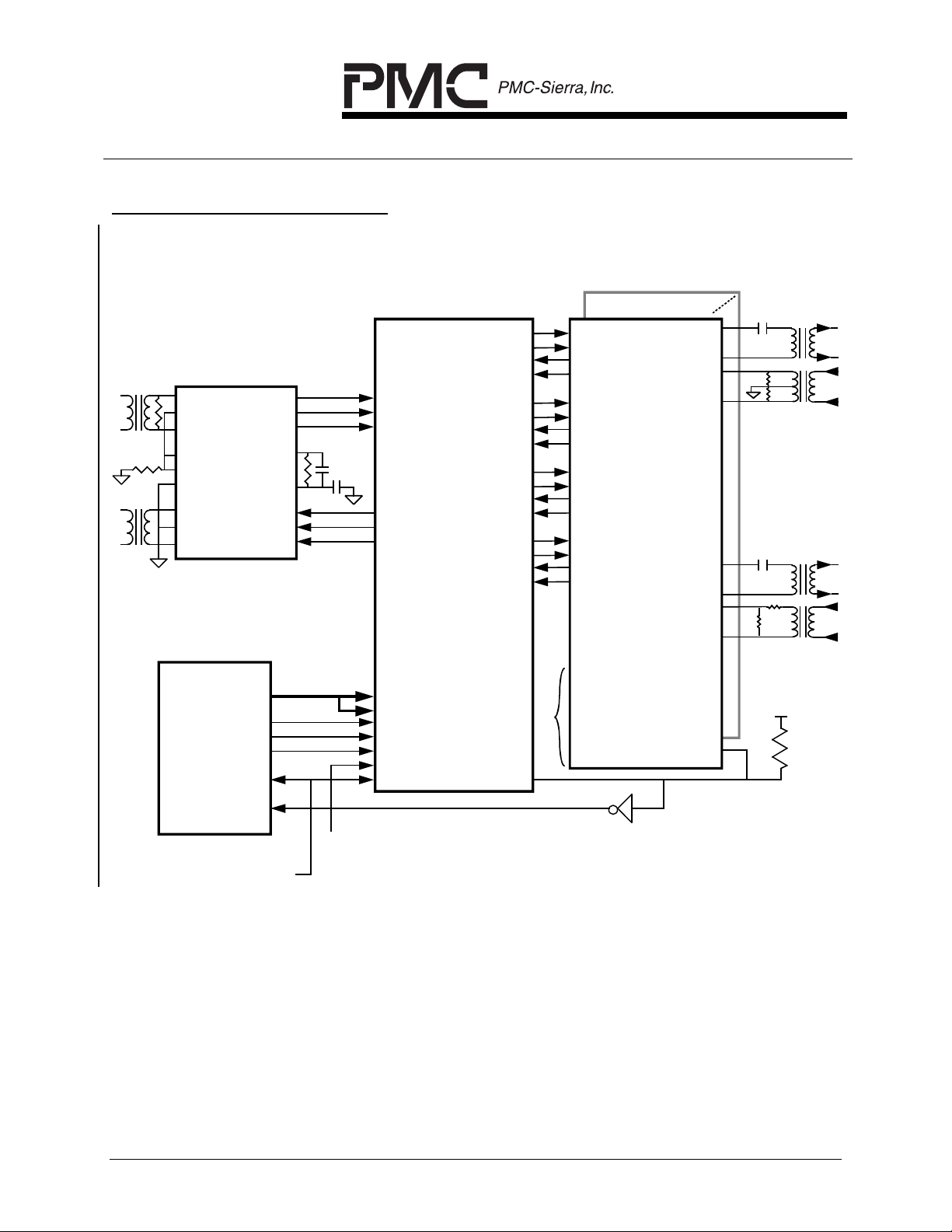
Figure 1 - M1-3 Multiplexer/Demultiplexer
(7 Quad DSX-1/E1 line interfaces)
•
•
•
•
•
•
•
•
•
1:1.36
1:2
1:1.36
1:2
+5V
LIN+
NC-R
LIN-
RGND
RFO
TGN D
LOUT+
NC-T
LOUT-
P
µ
e
fac
0
0
ter
72
P
In
8
ine
I 7
3 L
SS
DS-
AD[15:0]
ALE
RDB
WRB
RESB
INT
RPOS
RNEG
RCLK
LF1
LF2
TPOS
TNE G
TCLK
RPOS
RNEG
RCLK
TPOS
TNE G
TCLK
TICLK
TOH
TOH EN
TIMFP
TOHCLK
TOHFP
A[7:0]
D[7:0]
ALE
RDB
WRB
CSB
RSTB
RD1DAT1
RD1CLK1
TD1DAT1
TD1CLK1
RD1DAT2
RD1CLK2
TD1DAT2
TD1CLK2
RD1DAT3
RD1CLK3
TD1DAT3
TD1CLK3
MX
D3
RD1DAT4
3
RD1CLK4
TD1DAT4
31
TD1CLK4
PM8
RD1DAT28
RD1CLK28
TD1DAT28
TD1CLK28
INTB
TDD[1]
TCLKI[1]
RDD[1]
RCLKO[1]
TDD[2]
TCLKI[2]
RDD[2]
RCLKO[2]
TDD[3]
TCLKI[3]
RDD[3]
RCLKO[3]
TDD[4]
TCLKI[4]
RDD[4]
RCLKO[4]
•
•
•
•
•
A[8:0]
D[7:0]
ALE
RDB
WRB
from /to µP
CSB
RSTB
TXTIP[1]
TXRING[1]
RXTIP[1]
RXRING[1]
TXTIP[2]
TXRING[2]
RXTIP[2]
RXRING[2]
X
TXTIP[3]
S
TXRING[3]
RXTIP[3]
QD
RXRING[3]
4
1
TXTIP[4]
43
TXRING[4]
PM
RXTIP[4]
RXRING[4]
INTB
From chip select
decode circuitry
From Master
reset circu itry
Note:
Use of the SSI LIU as illustrated requires that TICLK has a duty cycle of 45% min
55% max or better (e.g. using a Connor Winfield S65T3 reference oscillator).
9
Page 20
PM8313 D3MX
DATA SHEET
PMC-920702 ISSUE 5 M13 MULTIPLEXER
5
TCLK
TPOS/TDAT
TNEG/TMFP
RCLK/VCLK
RPOS/RDAT
RNEG/RLCV
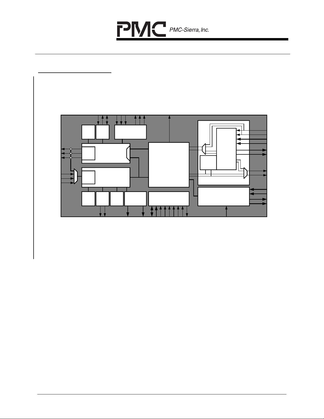
BLOCK DIAGRAM
LINT
TDLEOMI
TDLCLK/TD
XFDL
XBOC
FEAC
B3ZS
Encode
B3ZS
Decode
RBOC
FEAC
Tx
Rx
Tx
HDLC
TRAN
DS3 Transmit
Framer
FRMR
DS3 Receive
Framer
RFDL
Rx
HDLC
RDLCLK/RDLINT
RDLSIG/RDLEOM
TDLSIG/TDLUDR
PMON
Perf.
Monitor
TOH
TOHEN
O/H
Access
RMSFP, ROHP,
ROCLK, RODAT, RMFP,
TOHCLK
Tx
Rx
O/H
Access
ROHCLK,
TIMFP
TOHFP
TICLK
Microprocessor
D[7:0]
RE X Z , RAIS,
ROHFP, ROH, RLOS,
ROOF/RRED, RFERF
GD2CLK
MX23
M23
MUX/DEMUX
I/F
ALE
CSB
A[7:0]
A8/TRS
#1
TD1CLK4
TD1DAT4
MX12
M12 MUX/
DEMUX
DS2
FRMR
Framer
One of seven M12
#2-#7
Remaining Six M12
RDB
WRB
INTB
RSTB
TD2CLK
TD1DAT[3:1 ]
TD1CLK[3:1]
RD1DAT[3:1]
RD1CLK[3:1]
RD1CLK4
RD1DAT4
TD1CLK[28:5]
TD1DAT[28:5]
RD1CLK[28:5]
RD1DAT [28:5]
10
Page 21

PM8313 D3MX
DATA SHEET
PMC-920702 ISSUE 5 M13 MULTIPLEXER
DESCRIPTION
The PM8313 D3MX M13 Multiplexer supports asynchronous multiplexing and
demultiplexing of 28 DS1s, 21 E1s or 7 DS2s into a DS3 signal. The device
supports ANSI T1.107, Bell Communications Research TR-TSY-000009 and
CCITT Recommendation G.747 standards.
Receive DS3 framing is provided by the DS3 FRMR Framer Block. The FRMR
accepts either a B3ZS encoded bipolar, or a unipolar signal compatible with M23
and C-bit parity applications. The FRMR frames to a DS3 signal with a maximum
average reframe time of 1.5 ms in the presence of a 10
-3
bit error rate. The
FRMR indicates line code violations, loss of signal, framing bit errors, parity
errors, C-bit parity errors, and far end block errors (FEBE). The FRMR detects
far end receive failure (X-bits set to 0), the alarm indication signal (AIS), and the
idle signal. The FRMR is an off-line framer, indicating both out of frame (OOF)
and change of frame alignment (COFA) events. The error events (FER, CBIT
PARITY ERROR, FEBE, etc.) are still indicated while the framer is OOF, based
on the previous frame alignment.
The C-bit parity far end alarm channel (FEAC) and path maintenance data link
are supported. Bit oriented codes in the FEAC channel are detected by the
RBOC Bit-Oriented Code Receiver Block. If enabled, the RBOC generates an
interrupt when a valid code has been received. The path maintenance data link is
terminated using either the RFDL Data Link Receiver Block or an external HDLC
receiver. The RFDL supports polled, interrupt driven, and DMA servicing.
DS3 error event accumulation is provided by the DS3 PMON Performance
Monitor Block. The PMON accumulates framing bit errors, line code violations,
excessive zeros occurrences, parity errors, C-bit parity errors, and far end block
errors. Error accumulation continues even while the off-line framer is indicating
OOF. The counters are intended to be polled once per second, and are sized so
as not to saturate at a 10
-3
bit error rate. Transfer of count values to holding
registers is initiated through the microprocessor interface.
DS3 transmit framing insertion is provided by the DS3 TRAN Transmitter Block. It
outputs either a B3ZS encoded bipolar signal, or a unipolar signal. The DS3
TRAN inserts the X, P, M, C, and F bits into the outgoing DS3 stream. The DS3
TRAN block inserts far end receive failure, AIS, and the idle signal under the
control of external inputs, or internal register bits. Diagnostic features are
provided to allow the generation of line code violation error events, parity error
events, framing bit error events, and when enabled for the C-bit parity
application, C-bit parity error events, and far end block error events. External
11
Page 22

PM8313 D3MX
DATA SHEET
PMC-920702 ISSUE 5 M13 MULTIPLEXER
inputs allow substitution of the overhead bits or the sourcing of AIS, idle signal or
far end receive failure indication.
When configured for the C-bit parity application, bit oriented codes in the FEAC
channel are inserted by the XBOC Bit-Oriented Code Transmitter Block. The
FEAC code is controlled by an internal register. The path maintenance data link
is inserted using the XFDL Data Link Transmitter Block or an external HDLC
transmitter. The XFDL supports polled, interrupt driven, and DMA servicing.
The demultiplexing and multiplexing of seven 6312 kbit/s data streams into and
out of the DS3 is performed by the MX23 M23 Multiplexer Block. The MX23
contains FIFOs and performs bit stuffing fo r the rate adaptation of the DS2s. The
C-bits are set appropriately, with the option of inserting DS2 loopback requests.
The MX23 may be configured to generate an interrupt upon the detection of
loopback requests in the received DS3. AIS may be inserted in the any of the
6312 kbit/s tributaries in both directions. C-bit parity is supported by sourcing a
6.3062723 MHz clock, which corresponds to a stuffing ratio of 100%.
Framing to the demultiplexed 6312 kbit/s data streams is provided by the DS2
FRMR Framer. It supports both DS2 (ANSI TI.107) and CCITT Recommendation
G.747 frame formats. The maximum average reframe time is 7 ms for DS2 and
1ms for G.747. In DS2 mode, it detects far end receive failure and accumulates
M-bit and F-bit errors. In G.747 mode, it detects remote alarm and accumulates
framing word errors and parity errors. The DS2 FRMR is an off-line framer,
indication both OOF and COFA events. Error events (FERF, MERR, FERR,
PERR, RAI, framing word errors) are still indicated while the DS2 framer is
indicating OOF, based on the previous alignment.
The multiplexing and demultiplexing of the low speed tributaries into and out of a
6312 kbit/s data stream is performed by seven MX12 M12 Multiplexers. Each of
the MX12 blocks may be independently configured to multiplex and demultiplex
four 1544 kbit/s DS1s into and out of a DS2 formatted signal or to multiplex and
demultiplex three 2048 kbit/s signals into and out of a G.747 formatted signal.
Each MX12 may be independently bypassed so an external DS2 may by
multiplexed and demultiplexed directly into and out of the DS3. The MX12
contains FIFOs and performs bit stuffing to accommodate the tributary frequency
deviations. The C-bits are set appropriately, with the option of inserting DS1
loopback requests. The MX12 block may be configured to generate an interrupt
upon the detection of loopback requests in the received DS2. AIS may be
inserted in any of the low speed tributaries in both directions.
12
Page 23
PM8313 D3MX
DATA SHEET
PMC-920702 ISSUE 5 M13 MULTIPLEXER
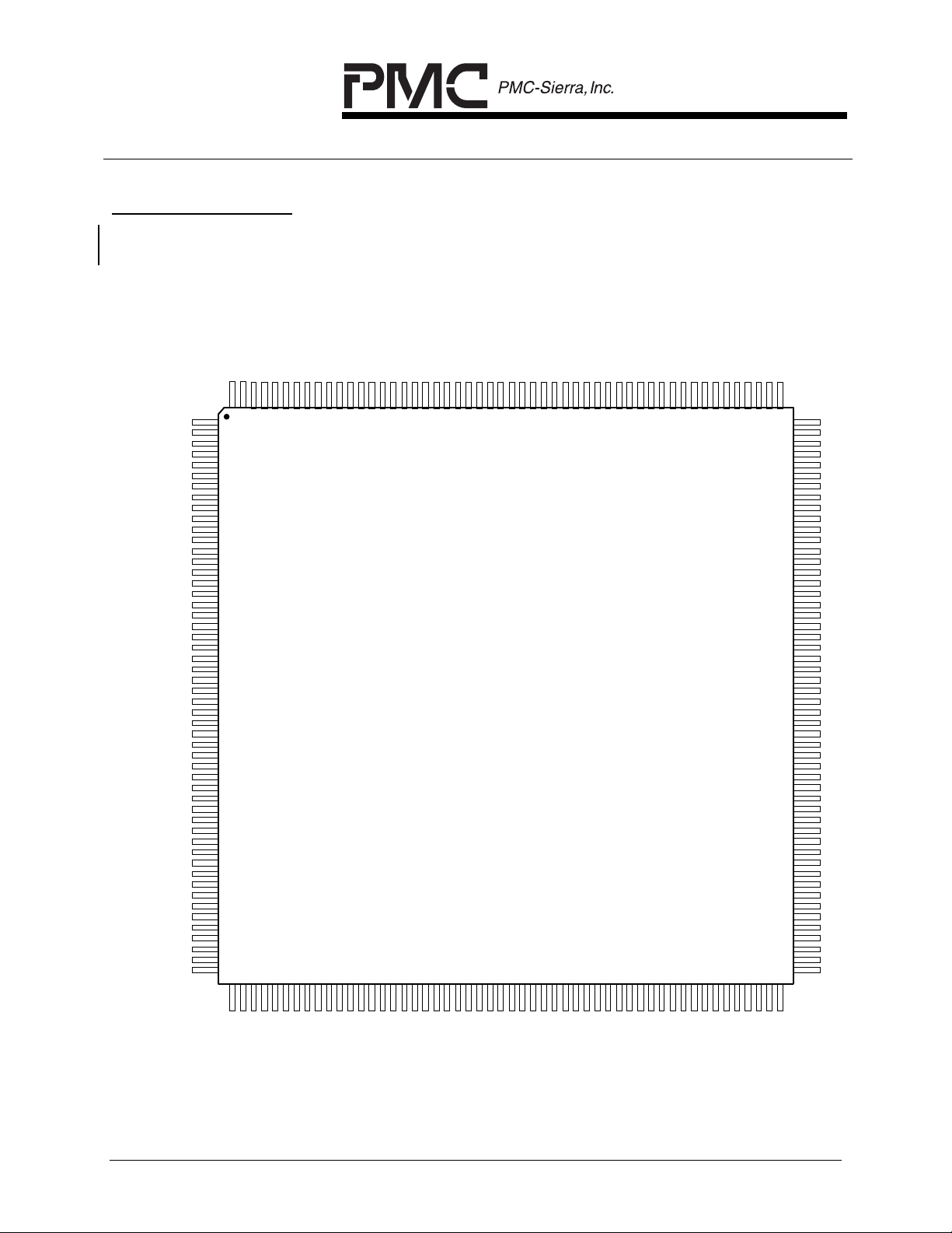
6
PIN DIAGRAM
The D3MX is packaged in a 208 pin PQFP package having a body size of 28 mm by 28
mm and a pin pitch of 0.5 mm.
RD1CLK2
VDDI
RD1DAT3
TD1DAT3
TD1CLK3
RD1CLK3
NC
TD1DAT4
VSSO
PM8313
D3MX
RD1DAT4
TD1CLK4
RD1CLK4
TD1DAT5
NC
RD1DAT5
TD1CLK5
TD1DAT6
RD1CLK5
RD1DAT6
TD1CLK6
NC
TD1DAT7
RD1DAT7
RD1CLK6
TD1CLK7
RD1CLK7
NC
VSSO
VDDO
TD1CLK8
TD1DAT8
RD1DAT8
RD1DAT9
TD1DAT9
RD1CLK8
PIN 157
PIN 1
TICLK
TCLK
TPOS/TDAT
RAIS
TNEG/TMFP
GD2CLK
RODAT
VSSO
VDDO
ROCLK
RMFP
ROHP
NC
TOHCLK
TOHFP
RMSFP
TOH
TOHEN
ROHFP
ROH
ROHCLK
RLOS
RFERF
ROOF/RRED
REXZ
RCLK/VCLK
VSSO
NC
RPOS/RDAT
RNEG/RLCV
RDLCLK/RDLINT
RDLSIG/RDLEOM
INTB
VSSO
NC
VDDO
CSB
ALE
D0
D1
D2
D3
D4
D5
D6
D7
A0
A1
A2
A3
A4
A5
PIN 52
TDLCLK/TDLING
TD2CLK
PIN 208
TIMFP
Index
TDLEOMI
TD1DAT1
RD1DAT1
TD1CLK1
TDLSIG/TDLUDR
VSSO
RD1CLK1NCTD1DAT2
VDDO
TD1CLK2
RD1DAT2NCVSSI
PIN 156
TD1CLK9
RD1CLK9
TD1DAT10
RD1DAT10
TD1CLK10
RD1CLK10
TD1DAT11
RD1DAT11
TD1CLK11
NC
RD1CLK11
TD1DAT12
RD1DAT12
TD1CLK12
RD1CLK12
TD1DAT13
NC
RD1DAT13
TD1CLK13
RD1CLK13
TD1DAT14
RD1DAT14
TD1CLK14
RD1CLK14
VSSO
NC
TD1DAT15
RD1DAT15
TD1CLK15
RD1CLK15
TD1DAT16
NC
RD1DAT16
TD1CLK16
RD1CLK16
VDDO
TD1DAT17
NC
RD1DAT17
TD1CLK17
RD1CLK17
TD1DAT18
RD1DAT18
NC
TD1CLK18
VSSO
RD1CLK18
TD1DAT19
RD1DAT19
TD1CLK19
RD1CLK19
TD1DAT20
PIN 105
A7
A6
PIN 53
A8
WRB
RDB
VSSI
RSTB
VDDI
NC
RD1CLK28
TD1CLK28
RD1CLK27
TD1DAT28
RD1DAT28
NC
TD1CLK27
RD1DAT27
TD1CLK26
TD1DAT27
RD1CLK26
NC
RD1DAT26
TD1DAT26
TD1CLK25
RD1CLK25
RD1DAT25NCTD1DAT25
VSSO
NC
TD1CLK24
RD1CLK24
RD1DAT24
TD1CLK23
TD1DAT24
RD1CLK23
TD1CLK22
RD1DAT23
TD1DAT23
RD1CLK22
NC
VDDO
RD1DAT22
VSSO
TD1DAT22
RD1CLK21
TD1CLK21
RD1DAT21
TD1DAT21
RD1CLK20
TD1CLK20
RD1DAT20
PIN 104
13
Page 24

PM8313 D3MX
DATA SHEET
PMC-920702 ISSUE 5 M13 MULTIPLEXER
7
PIN DESCRIPTION
Pin Name Type Pin No. Function
RCLK/
VCLK
Input 26 The receive input clock (RCLK) provides timing
for the receive side of the D3MX. RCLK is
nominally a 44.736 MHz, 50% duty cycle clock.
The test vector clock (VCLK) signal is used
during D3MX production testing to verify
internal functionality.
RPOS/
RDAT
Input 29 The positive input pulse (RPOS) signal
represents the positive pulses received on the
B3ZS-encoded line when configured for dual
rail reception. The receive data input (RDAT)
signal represents the unipolar DS3 input
stream when configured for single rail
operation. Both RPOS and RDAT are sampled
on the rising edge of RCLK by default and may
be enabled to be sampled on the falling edge of
RCLK.
RNEG/
RLCV
Input 30 The negative input pulse (RNEG) signal
represents the negative pulses received on the
B3ZS-encoded line when configured for dual
rail reception. Line code violations (LCVs) may
be input on the receive line code violation
(RLCV) signal when configured for single rail
operation. Both RNEG and RLCV are sampled
on the rising edge of RCLK by default and may
be enabled to be sampled on the falling edge of
RCLK.
ROCLK Output 10 The receive output clock (ROCLK) signal
provides timing for downstream processing.
ROCLK is nominally a 44.736 MHz, 50% duty
cycle clock. RODAT, RMFP, RMSFP, RLOS,
REXZ and ROHP are updated on the falling
edge of ROCLK. ROCLK is a buffered version
of RCLK.
14
Page 25

PM8313 D3MX
DATA SHEET
PMC-920702 ISSUE 5 M13 MULTIPLEXER
Pin Name Type Pin No. Function
RODAT Output 7 The receive data output (RODAT) signal carries
the 44.736 Mbit/s NRZ stream decoded from
the B3ZS line signal. The frame alignment
signals (RMFP, RMSFP, and ROHP) are
aligned to the RODAT stream. RODAT is
updated on the falling edge of ROCLK.
RMFP Output 11 The receive M-frame pulse (RMFP) signal
marks the first bit (X1) in the M-frame of the
DS3 signal on RODAT. When the framer is out-
of-frame, RMFP continues to operate with
timing aligned to the old M-frame position.
When the framer regains frame alignment the
RMFP timing is updated, which may result in a
change of frame alignment. RMFP is updated
on the falling edge of ROCLK.
RMSFP Output 16 The receive M-subframe pulse (RSMFP) signal
marks the first bit (X, P, and M) in each M-
subframe of the received DS3 stream (RODAT)
when the framer is in-frame. When the framer
is out-of-frame, RSMFP continues to operate
with timing aligned to the old M-frame position.
When the framer regains frame alignment the
RMSFP timing is updated, which may result in
a change of frame alignment. RSMFP is
updated on the falling edge of ROCLK.
ROHP Output 12 The receive overhead pulse (ROHP) signal
marks the overhead bit positions (X, P, M, C,
and F) in the received DS3 stream (RODAT)
when the framer is in-frame. When the framer
is out-of-frame, ROHP continues to operate
with timing aligned to the old M-frame position.
When the framer regains frame alignment the
ROHP timing is updated, which may result in a
change of frame alignment. ROHP is updated
on the falling edge of ROCLK.
15
Page 26

PM8313 D3MX
DATA SHEET
PMC-920702 ISSUE 5 M13 MULTIPLEXER
Pin Name Type Pin No. Function
ROHCLK Output 21 The receive overhead clock (ROHCLK) cycles
once per overhead bit. ROHCLK is nominally a
526 kHz clock. ROOF, RFERF, RAIS, RIDL,
RFERR, ROH, and ROHFP are updated on the
falling edge of ROHCLK.
ROH Output 20 The receive overhead data (ROH) signal
contains the overhead bits (C, F, X, P, and M)
extracted from the received DS3 stream. ROH
is updated on the falling edge of ROHCLK.
ROHFP Output 19 The receive overhead frame position (ROHFP)
signal may be used to locate the individual
overhead bits in the received overhead data
stream, ROH. ROHFP is high during the X1
overhead bit position in the ROH stream.
ROHFP is updated on the falling edge of
ROHCLK.
RLOS Output 22 The receive loss of signal (RLOS) status is set
high when the dual rail NRZ format stream is
selected, and 175 successive zeros are
detected on the RPOS and RNEG inputs.
RLOS is set low when the ones' density is
greater than 33% for 175 ± 1 bit periods on the
RPOS and RNEG inputs. RLOS is updated on
the falling edge of ROCLK.
REXZ Output 25 The receive excessive zero (REXZ) signal
indicates the presence of 3 or more
consecutive zeros in the received DS3 bipolar
stream. REXZ pulses high for one ROCLK
cycle whenever 3 or more consecutive zeros
are detected. When the Receive DS3 interface
is configured to for uni-polar data, the REXZ
output is forced low. REXZ is updated on the
falling edge of ROCLK.
16
Page 27

PM8313 D3MX
DATA SHEET
PMC-920702 ISSUE 5 M13 MULTIPLEXER
Pin Name Type Pin No. Function
RAIS Output 4 The receive alarm indication signal (RAIS)
indicates the presence of AIS in the received
DS3 stream. RAIS is set high when the AIS
pattern has been received for 2.23 ms or 13.5
ms (software selectable). RAIS is set low when
the AIS pattern has not been received for 2.23
ms or 13.5 ms. RAIS is updated on the falling
edge of ROHCLK.
ROOF/ Output 24 The receive out-of-frame (ROOF) signal is set
high when an out-of-frame condition is
declared. An out-of-frame is declared when 3
out of 16 (default) or 3 out of 8 consecutive F-
bit errors are detected, or when one or more M-
bit errors is detected in 3 out of 4 consecutive
M-frames. ROOF is set low when an in-frame
condition is declared. ROOF is updated on the
falling edge of ROHCLK. This ROOF signal is
available when the REDO bit in the Master
Alarm Enable register is logic 0.
RRED The receive RED Alarm (RRED) signal is
available when the REDO bit in the Master
Alarm Enable register is logic 1. The RRED
output is set high when a DS3 out-of-frame
condition or DS3 loss of signal condition has
been present for either 2.23ms or 13.5 ms. The
RRED output is set low when a DS3 out-of-
frame condition or DS3 loss of signal condition
has been absent for either 2.23ms or 13.5 ms.
RRED is updated on the falling edge of
ROHCLK.
17
Page 28
PM8313 D3MX
DATA SHEET
PMC-920702 ISSUE 5 M13 MULTIPLEXER
Pin Name Type Pin No. Function
RFERF Output 23 The receive far end receive failure (RFERF)
signal reflects the value of the internal FERF
state buffered by two M-frames. Internally,
FERF is set high when both X-bits (X1 and X2)
are received as logic 0 in the current M-frame;
FERF is set low when both X-bits are received
as logic 1. FERF remains in its previous state
when X1 • X2 in the current M-frame. The
RFERF output latency provides a better than
99.99% chance of freezing (i.e. holding RFERF
in its previous state) upon a valid state value
during the occurrence of an out of frame.
RFERF is updated once per M-frame on the
falling edge of ROHCLK.
18
Page 29

PM8313 D3MX
DATA SHEET
PMC-920702 ISSUE 5 M13 MULTIPLEXER
Pin Name Type Pin No. Function
RDLCLK/
RDLINT
Output 31 The receive data link clock (RDLCLK) signal is
active when an external HDLC receiver is
selected (the REXHDLC bit in the Master
HDLC Configuration Register is a logic 1). The
RDLCLK signal provides timing for the external
processing of the path maintenance data link
signal extracted by the DS3 FRMR. RDLCLK is
updated on the falling edge of the ROHCLK
signal and cycles 3 times per M-frame.
RDLCLK is nominally a 28.2 kHz clo ck, which
is low for at least 1.9 µs per cycle.
The data link interrupt (RDLINT) signals is
active when the internal HDLC receiver is
selected (the REXHDLC in the Master HDLC
Configuration Register bit is a logic 0). The
RDLINT signal is asserted when an event
occurs which changes the status of the HDLC
receiver. RDLINT is updated on the falling
edge of the ROHCLK signal. RDLINT is
deasserted when the Interrupt Enable/Status
Register is read in the HDLC receiver. By
default RDLINT is an active low open-drain
output, but can be configured as active high.
Typically, RDLINT would be connected to an
external DMA device. If the supervising
microprocessor is desired to service the RFDL,
this output can be wired-ORed with the INTB
output when RDLINT is configured as an
active-low open drain output.
19
Page 30

PM8313 D3MX
DATA SHEET
PMC-920702 ISSUE 5 M13 MULTIPLEXER
Pin Name Type Pin No. Function
RDLSIG/
RDLEOM
Output 32 The receive data link (RDLSIG) signal is active
when an external HDLC receiver is selected
(the REXHDLC bit in the corresponding Master
HDLC Configuration Register is a logic 1). The
RDLSIG signal carries bits extracted from the
three C-bits in M-subframe #5 by the DS3
framer. RDLSIG is held high when C-bit parity
mode is not enabled. RDLSIG is updated on
the falling edge of the corresponding RDLCLK
signal.
The receive end of message (RDLEOM) signal
is active if the internal HDLC receiver is
selected (the REXHDLC bit in the Master
HDLC Configuration Register is a logic 0). The
RDLEOM signal is asserted when the last byte
of a sequence is read from the HDLC receiver,
or if the receiver's buffer overruns. RDLEOM is
updated on the falling edge of the ROHCLK
signal. RDLEOM is deasserted when the
Interrupt Enable/Status Register is read in the
HDLC Receiver. By default, RDLEOM is an
active low open-drain output, but can be
configured as active high.
Typically, RDLEOM would be connected to the
supervising microprocessor when an external
DMA is used, signaling the microprocessor that
a complete message is ready. In this case the
RDLEOM is configured as an active-low open
drain output and wired-ORed with the INTB
output.
20
Page 31

PM8313 D3MX
DATA SHEET
PMC-920702 ISSUE 5 M13 MULTIPLEXER
Pin Name Type Pin No. Function
RD1CLK1
RD1CLK2
RD1CLK3
RD1CLK4
RD1CLK5
RD1CLK6
RD1CLK7
RD1CLK8
RD1CLK9
RD1CLK10
RD1CLK11
RD1CLK12
RD1CLK13
RD1CLK14
RD1CLK15
RD1CLK16
RD1CLK17
RD1CLK18
RD1CLK19
RD1CLK20
RD1CLK21
Output 198
193
186
180
175
170
166
159
155
151
146
142
137
133
127
122
116
110
106
102
98
The receive DS1 clock (RD1CLK[28:1]) signals
provide timing for each of the 28 demultiplexed
DS1 streams. The RD1CLK[28:1] signals are
nominally 1.544 MHz clocks, but have
substantial jitter due to the demultiplexing and
destuffing processes. The RD1DAT[28:1]
outputs are updated on the falling edges of the
corresponding RD1CLK[28:1] signals.
When the internal M12 multiplexers are
configured for G.747 multiplexing, every fourth
RD1CLK signal (RD1CLK4, 8, 12, 16, 20, 24,
28) is unused and held low. The remaining
RD1CLK signals are then nominally 2.048 MHz
clocks.
When the internal M12 multiplexers are
bypassed, every fourth RD1CLK signal
(RD1CLK4, 8, 12, 16, 20, 24, 28) may become
a DS2 rate clock operating at nominally 6.312
MHz. The remaining RD1CLK signals for the
particular M12 multiplexer bypassed are then
unused and held low.
The internal M12 multiplexers may be
bypassed or configured for G.747 multiplexing
on an individual basis. Thus the configuration
of each of the seven blocks of four RD1CLK
signals is independently programmable.
RD1CLK22
RD1CLK23
RD1CLK24
RD1CLK25
RD1CLK26
RD1CLK27
RD1CLK28
91
87
82
76
71
66
62
21
Page 32

PM8313 D3MX
DATA SHEET
PMC-920702 ISSUE 5 M13 MULTIPLEXER
Pin Name Type Pin No. Function
RD1DAT1
RD1DAT2
RD1DAT3
RD1DAT4
RD1DAT5
RD1DAT6
RD1DAT7
RD1DAT8
RD1DAT9
RD1DAT10
RD1DAT11
RD1DAT12
RD1DAT13
RD1DAT14
RD1DAT15
RD1DAT16
RD1DAT17
RD1DAT18
RD1DAT19
Output 202
195
188
182
177
173
168
161
157
153
149
144
139
135
129
124
118
114
108
The receive DS1 data (RD1DAT[28:1]) signals
carry the 28 demultiplexed DS1 streams. The
RD1DAT[28:1] outputs are updated on the
falling edges of the corresponding
RD1CLK[28:1] signals.
When the internal M12 multiplexers are
configured for G.747 multiplexing, every fourth
RD1DAT signal (RD1DAT4, 8, 12, 16, 20, 24,
28) is unused and held low. The remaining
RD1DAT signals are then nominally 2.048
Mbit/s data streams.
When the internal M12 multiplexers are
bypassed, every fourth RD1DAT signal
(RD1DAT4, 8, 12, 16, 20, 24, 28) may become
a DS2 rate data stream operating at nominally
6.312 Mbit/s. The remaining RD1DAT signals
for the particular M12 multiplexer bypassed are
then unused and held low.
The internal M12 multiplexers may be
bypassed or configured for G.747 multiplexing
on an individual basis. Thus the configuration
of each of the seven blocks of four RD1DAT
signals is independently programmable.
RD1DAT20
RD1DAT21
RD1DAT22
RD1DAT23
RD1DAT24
RD1DAT25
RD1DAT26
RD1DAT27
RD1DAT28
104
100
94
89
84
78
74
69
64
22
Page 33

PM8313 D3MX
DATA SHEET
PMC-920702 ISSUE 5 M13 MULTIPLEXER
Pin Name Type Pin No. Function
TD1CLK1
TD1CLK2
TD1CLK3
TD1CLK4
TD1CLK5
TD1CLK6
TD1CLK7
TD1CLK8
TD1CLK9
TD1CLK10
TD1CLK11
TD1CLK12
TD1CLK13
TD1CLK14
TD1CLK15
TD1CLK16
TD1CLK17
TD1CLK18
TD1CLK19
TD1CLK20
TD1CLK21
Input 201
194
187
181
176
172
167
160
156
152
148
143
138
134
128
123
117
112
107
103
99
The transmit DS1 clock (TD1CLK[28:1]) signals
provide timing for each of the 28 DS1 streams
to be multiplexed. The TD1CLK[28:1] signals
should nominally be 1.544 MHz clocks, and
should have the minimal jitter and wander of a
standard DS1 line signal. The TD1DAT[28:1]
inputs are sampled on the rising edges of the
corresponding TD1CLK[28:1] signals.
When the internal M12 multiplexers are
configured for G.747 multiplexing, every fourth
TD1CLK signal (TD1CLK4, 8, 12, 16, 20, 24,
28) is unused and ignored. The remaining
TD1CLK signals should then nominally be
2.048 MHz clocks.
When the internal M12 multiplexers are
bypassed, every fourth TD1CLK signal
(TD1CLK4, 8, 12, 16, 20, 24, 28) should then
become a DS2 rate clock operating at
nominally 6.312 MHz. The remaining TD1CLK
signals for the particular M12 multiplexer
bypassed are then unused and ignored.
The internal M12 multiplexers may be
bypassed or configured for G.747 multiplexing
on an individual basis. Thus the configuration
of each of the seven blocks of four TD1CLK
signals is independently programmable.
TD1CLK22
TD1CLK23
TD1CLK24
TD1CLK25
TD1CLK26
TD1CLK27
TD1CLK28
92
88
83
77
72
68
63
23
Page 34

PM8313 D3MX
DATA SHEET
PMC-920702 ISSUE 5 M13 MULTIPLEXER
Pin Name Type Pin No. Function
TD1DAT1
TD1DAT2
TD1DAT3
TD1DAT4
TD1DAT5
TD1DAT6
TD1DAT7
TD1DAT8
TD1DAT9
TD1DAT10
TD1DAT11
TD1DAT12
TD1DAT13
TD1DAT14
TD1DAT15
TD1DAT16
TD1DAT17
TD1DAT18
TD1DAT19
Input 203
196
190
184
179
174
169
162
158
154
150
145
141
136
130
126
120
115
109
The transmit DS1 data (TD1DAT[28:1]) signals
carry the 28 DS1 streams to be multiplexed.
The TD1DAT[28:1] inputs are sampled on the
rising edges of the corresponding
TD1CLK[28:1] signals.
When the internal M12 multiplexers are
configured for G.747 multiplexing, every fourth
TD1DAT signal (TD1DAT4, 8, 12, 16, 20, 24,
28) is unused and ignored. The remaining
TD1DAT signals should then nominally be
2.048 Mbit/s data streams.
When the internal M12 multiplexers are
bypassed, every fourth TD1DAT signal
(TD1DAT4, 8, 12, 16, 20, 24, 28) may become
a DS2 rate data stream operating at nominally
6.312 Mbit/s. The remaining TD1DAT signals
for the particular M12 multiplexer bypassed are
then unused and ignored.
The internal M12 multiplexers may be
bypassed or configured for G.747 multiplexing
on an individual basis. Thus the configuration
of each of the seven blocks of four TD1DAT
signals is independently programmable.
TD1DAT20
TD1DAT21
TD1DAT22
TD1DAT23
TD1DAT24
TD1DAT25
TD1DAT26
TD1DAT27
TD1DAT28
105
101
97
90
86
81
75
70
65
24
Page 35

PM8313 D3MX
DATA SHEET
PMC-920702 ISSUE 5 M13 MULTIPLEXER
Pin Name Type Pin No. Function
GD2CLK Output 6 The transmit generated DS2 clock (GD2CLK)
signal is provided for use in integrated M13 or
C-bit parity multiplex applications. When
configured for M13 operation, GD2CLK is
nominally a 6.311993 MHz clock, which
corresponds to a stuffing ratio of 39.1%. When
configured for C-bit parity operation, GD2CLK
is nominally a 6.3062723 MHz clock, which
corresponds to a stuffing ratio of 100%. The
GD2CLK may be connected to the TD2CLK
input clock. GD2CLK is updated on the falling
edge of TCLK.
TD2CLK Input 206 The transmit DS2 clock (TD2CLK) signal
provides timing for the multiplex side of all of
the MX12 TSBs. TD2CLK is nominally a 6.312
MHz, 50% duty cycle clock.
25
Page 36

PM8313 D3MX
DATA SHEET
PMC-920702 ISSUE 5 M13 MULTIPLEXER
Pin Name Type Pin No. Function
TDLSIG/
TDLUDR
I/O 205 The transmit data link (TDLSIG) signal is active
when an external HDLC receiver is selected
(the TEXHDLC bit in the corresponding Master
HDLC Configuration Register is a logic 1). The
TDLSIG signal carries bits to be inserted in the
three C-bits in M-subframe #5 by the DS3
transmitter. TDLSIG is ignored when C-bit
parity mode is not enabled. TDLSIG is
sampled on the rising edge of the TDLCLK
signal.
The transmit data link underrun (TDLUDR)
signal is active when the internal HDLC
receiver is selected (the TEXHDLC bit in the
corresponding Master HDLC Configuration
Register is a logic 0). TDLUDR is asserted
when the internal HDLC transmitter underruns.
TDLUDR is deasserted by writing to the XFDL
Interrupt Status Register. By default TDLUDR
is an active low open-drain output, but can be
configured as active high.
Upon a reset, the TEXHDLC bit a logic 1, thus,
the pin is configured as an input, TDLSIG.
Typically, TDLUDR would be connected to the
supervising microprocessor when an external
DMA is used, signaling the microprocessor that
a severe error has occurred causing the
transmit buffer to underrun. In this case the
TDLUDR is configured as an active-low open
drain output and wired-ORed with the INTB
output.
26
Page 37

PM8313 D3MX
DATA SHEET
PMC-920702 ISSUE 5 M13 MULTIPLEXER
Pin Name Type Pin No. Function
TDLCLK/
TDLINT
Output 207 The transmit data link clock (TDLCLK) signal is
active when an external HDLC receiver is
selected (the TEXHDLC bit in the Master HDLC
Configuration Register is a logic 1). The
TDLCLK signal provides timing for the external
sourcing of the path maintenance data link
signal inserted by the DS3 TRAN. TDLCLK is
updated on the falling edge of the TOHCLK
signal and cycles 3 times per M-frame.
TDLCLK is nominally a 28.2 kHz clock, which is
low for at least 1.9 µs per cycle.
The transmit data link interrupt (TDLINT) signal
is active when the internal HDLC transmitter is
selected (the TEXHDLC bit in the
corresponding Master HDLC Configuration
Register is a logic 0).TDLINT is asserted when
the last data byte written to the internal HDLC
transmitter has been setup fo r transmission,
and a write is required to the XFDL
Configuration Register, or the XFDL Transmit
Data Register to either end the current
message transmission, or to provide more
data. By default TDLINT is an active low open-
drain output, but can be configured as active
high.
Typically, TDLINT would be connected to an
external DMA device. If the supervising
microprocessor is desired to service the XFDL,
this output can be wired-ORed with the INTB
output when TDLINT is configured as an active-
low open drain output.
27
Page 38

PM8313 D3MX
DATA SHEET
PMC-920702 ISSUE 5 M13 MULTIPLEXER
Pin Name Type Pin No. Function
TDLEOMI Input 204 The transmit data link end of message input
(TDLEOMI) provides a method for an external
DMA controller to signal the end of the
transmitted message to the HDLC transmitter
without needing to write to the XFDL
Configuration Register. The TDLEOMI input is
active high and must be glitch-free. It internally
sets the corresponding EOM register bit in the
XFDL Configuration register. The TDLEOMI
input may be asserted during or after the write
of the last byte of a packet but before the next
byte would be expected (within 210 µs of the
last assertion of TDLINT or the INT bit in the
XFDL Status Register). TDLEOMI must be
deasserted before the write of the first byte of
the next packet. TDLEOMI is ignored if no data
transmission is pending.
TICLK Input 1 The transmit input clock (TICLK) provides the
transmit direction timing. TICLK is nominally a
44.736 MHz, 50% duty cycle clock. TIMFP is
sampled on the rising edge of TICLK.
TIMFP Input 208 The transmit M-frame pulse input (TIMFP)
signal allows one to control the alignment of the
M-frame of the transmitted DS3 stream (TDAT).
The first bit (X1) of the M-frame on TDAT will
occur within several TICLK cycles and be
identified by the TMFP output signal. TIMFP
may be tied low if such control is not required.
TIMFP is sampled on the rising edge of TICLK.
TOH Input 17 The transmit overhead data (TOH) signal
contains the overhead bits (C, F, X, P, and M)
that may be inserted in the transmitted DS3
stream. TOH is sampled on the rising edge of
TOHCLK.
28
Page 39

PM8313 D3MX
DATA SHEET
PMC-920702 ISSUE 5 M13 MULTIPLEXER
Pin Name Type Pin No. Function
TOHEN Input 18 The transmit overhead insertion (TOHEN)
signal controls the insertion of DS3 overhead
bits from the TOH input. When TOHEN is high,
the associated overhead bit in the TOH stream
is inserted in the transmitted DS3 frame. When
TOHEN is low, the DS3 overhead bit is
generated and inserted internally. TOHEN is
sampled on the rising edge of TOHCLK.
TOHFP Output 15 The transmit overhead frame position (TOHFP)
signal may be used to align the individual
overhead bits in the transmitted overhead data
stream, TOH, to the DS3 M-frame. TOHFP is
high during the X1 overhead bit position in the
TOH stream. TOHFP is updated on the falling
edge of TOHCLK.
TOHCLK Output 14 The transmit overhead clock (TOHCLK) cycles
once per overhead bit. TOHCLK is nominally a
526 kHz clock. TOHFP is updated on the falling
edge of T OHCLK. T OH, and TOHEN are
sampled on the rising edge of TOHCLK.
TCLK Output 2 The transmit clock (TCLK) provides timing for
circuitry downstream of the DS3 transmitter of
the D3MX. TCLK is nominally a 44.736 MHz,
50% duty cycle clock.
TPOS/
TDAT
Output 3 The transmit positive pulse (TPOS) signal
represents the positive pulses transmitted on
the B3ZS-encoded line when configured for
dual-rail operation. TPOS is updated on the
falling edge of TCLK by default but may be
enabled to be updated on the rising edge of
TCLK.
The transmit data output (TDAT) signal
represents a unipolar DS3 output stream when
configured for single rail operation. TDAT is
updated on the falling edge of TCLK by default
but may be enabled to be updated on the r ising
edge of TCLK.
29
Page 40

PM8313 D3MX
DATA SHEET
PMC-920702 ISSUE 5 M13 MULTIPLEXER
Pin Name Type Pin No. Function
TNEG/
TMFP
Output 5 The transmit negative pulse (TNEG) signal
represents the negative pulses transmitted on
the B3ZS-encoded line when configured for
dual rail operation. TNEG is updated on the
falling edge of TCLK by default but may be
enabled to be updated on the rising edge of
TCLK.
The transmit multiframe pulse (TMFP) signal
marks the transmit M-frame alignment when
configured for single rail operation. The TMFP
output is high during the first bit (X1) of the
DS3 multiframe presented on TDAT. TMFP is
updated on the falling edge of TCLK by default
but may be enabled to be updated on the r ising
edge of TCLK.
INTB Output 33 The active low interrupt (INTB) signal goes low
when one of the DS3 FRMR, RBOC, DS2
FRMR, MX12, MX23 or PMON TSBs generates
an interrupt, provided that the interrupt source
in question is not masked. INTB goes high
when the Interrupt Enable/Status Register is
read in the corresponding TSB. Note that INTB
will remain low until all active, unmasked
interrupt sources are acknowledged. The INTB
signal is an open drain output.
CSB Input 45 The active low chip select (CSB) signal is low
during D3MX register accesses. CSB mu st go
high at least once after a powerup to clear
internal test modes. If CSB is not used, then it
should be tied to an inverted version of RSTB,
in which case RDB and WRB determine
register accesses
RDB Input 57 The active low read enable (RDB) signal is low
during D3MX register read accesses. The
D3MX drives the D7-D0 bus with the contents
of the addressed register while RDB and CSB
are low.
30
Page 41

PM8313 D3MX
DATA SHEET
PMC-920702 ISSUE 5 M13 MULTIPLEXER
Pin Name Type Pin No. Function
WRB Input 56 The active low write strobe (WRB) signal is low
during a D3MX register write access. The D7-
D0 bus contents are clocked into the
addressed register on the rising WRB edge
while CSB is low.
D0
D1
D2
D3
D4
D5
D6
D7
A0
A1
A2
A3
A4
A5
A6
I/O 34
35
37
38
39
41
42
44
Input 47
48
49
50
51
52
53
The bidirectional data bus (D7-D0) is used
during D3MX register read and write accesses.
The address bus (A8-A0) selects specific
registers during D3MX register accesses.
A7
54
A8/TRS 55 The test register select (TRS) signal
discriminates between normal and test mode
register accesses. TRS is high during test
mode register accesses, and is low during
normal mode register accesses. The TRS input
has an integral pull down resistor.
TRS should be connected to ground for normal
mode register access.
RSTB Input 58 The active low reset (RSTB) signal provides an
asynchronous D3MX reset. RSTB is a Schmitt
triggered input with an integral pull up resistor.
31
Page 42

PM8313 D3MX
DATA SHEET
PMC-920702 ISSUE 5 M13 MULTIPLEXER
Pin Name Type Pin No. Function
ALE Input 46 The address latch enable (ALE) is active high
and latches the address bus (A7-A0) and TRS
when low. When ALE is high, the internal
address latches are transparent. It allows the
D3MX to interface to a multiplexed
address/data bus. The ALE input has an
integral pull up resistor.
VDDI1
VDDI2
VSSI1
VSSI2
VDDO1
VDDO2
VDDO3
VDDO4
VDDO5
VDDO6
VSSO1
VSSO2
VSSO3
VSSO4
VSSO5
Power 60
189
Ground 59
191
Power 199
9
43
95
121
164
Ground 200
8
36
96
111
The core power (VDDI) pins should be
connected to a well decoupled +5 V DC in
common with VDDO.
The core ground (VSSI) pins should be
connected to GND in common with VSSO.
The pad ring power (VDDO) pins should be
connected to a well decoupled +5 V DC in
common with VDDI.
The pad ring ground (VSSO) pins should be
connected to GND in common with VSSI.
VSSO6
VSSO7
VSSO8
VSSO9
VSSO10
163
183
27
80
132
32
Page 43

PM8313 D3MX
DATA SHEET
PMC-920702 ISSUE 5 M13 MULTIPLEXER
Notes on Pin Description:
All D3MX inputs and bidirectionals present minimum capacitive loading and
operate at TTL logic levels.
All D3MX digital outputs and bidirectionals have 2 mA drive capability, except the
INTB, TPOS/TDAT, TNEG/TMFP, TCLK, ROCLK, RODAT, RMFP, RMSFP, ROHP
outputs and the D7-D0 bidirectionals, which have 4 mA drive capability.
The VSSO and VSSI ground pins are not internally connected together. Failure
to connect these pins externally may cause malfunction or damage the D3MX.
The VDDO and VDDI power pins are not internally connected together. Failure to
connect these pins externally may cause malfunction or damage the D3MX.
208-pin QFP pins # 13, 28, 40, 61, 67, 73, 79, 85, 93, 113, 119, 125, 131, 140,
147, 165, 171, 178, 185, 192, 197 are all "no-connect".
33
Page 44

PM8313 D3MX
DATA SHEET
PMC-920702 ISSUE 5 M13 MULTIPLEXER
8
FUNCTIONAL DESCRIPTION
8.1 DS3 Framer
The DS3 Framer (FRMR) Block integrates circuitry required for decoding a
B3ZS-encoded signal and framing to the resulting DS3 bit stream. The FRMR is
directly compatible with the M23 and C-bit parity DS3 applications.
The FRMR decodes a B3ZS-encoded signal and provides indications of line
code violations. The B3ZS decoding algorithm and the LCV definition can
independently be chosen via software. Loss of signal is also detected.
The framing algorithm examines five F-bit candidates simultaneously. When at
least one discrepancy has occurred in all the candidates, the algorithm examines
the next set of candidates. When a single F-bit candidate remains in a set, the
first bit in the supposed M-subframe is examined for the M-frame alignment
signal (i.e. the M-bits, M1,M2,M3, are following the 010 pattern). Framing is
declared if the M-bits are correct for three consecutive M-frames while no
discrepancies have occurred in the F-bits. During the examination of the M-bits
the X-bits and P-bits are ignored. The algorithm gives a maximum average
reframe time of less than 1.5 ms.
Once in-frame, the FRMR provides indications of the M-frame and M-subframe
boundaries, and identifies the overhead bit positions in the incoming DS3 signal.
While the FRMR is in-frame, the F-bit and M-bit positions in the DS3 stream are
examined. Out-of-frame is declared when 3 F-bit errors out of 16 consecutive Fbits or 8 consecutive F-bits are observed (selectable by the M3O8 bit), or when
one or more M-bit errors are detected in 3 out of 4 consecutive M-frames. The
M-bit error criteria for OOF can be disabled via the MBDIS bit in the DS3 Framer
configuration register. The 3 out of 8 consecutive F-bits out-of-frame ratio
-
provides more robust operation in the presence of a 10
3
bit error rate than the 3
out of 16 consecutive F-bits ratio (less than one false OOF every minute verses
one false OOF every 6 seconds, respectively); either choice of out-of-frame ratios
allows an out-of-frame to be declared quickly when the M-subframe alignment
patterns or, optionally, when the M-frame alignment is lost.
Also while in-frame, M-bit or F-bit framing bit errors and P-bit parity errors are
indicated. When C-bit parity mode is enabled, both C-bit parity errors and far
end block errors are indicated. These error indications, as well as the line code
violation and excessive zeros indication, may be accumulated over 1 second
intervals with the T3 Performance Monitor (PMON). Note that the framer is an
34
Page 45

PM8313 D3MX
DATA SHEET
PMC-920702 ISSUE 5 M13 MULTIPLEXER
off-line framer, indicating both OOF and COFA events. Even if an OOF is
indicated, the framer will continue indicating performance monitoring information
based on the previous frame alignment.
Status signals such as the RED alarm, alarm indication signal, and the idle
signal are detected. The framer employs a simple integration algorithm (with a
1:1 slope) that is based on the occurrence of "valid" M-frame intervals. For the
RED alarm, an M-frame is said to be a "valid" interval if it contains a RED defect,
defined as an occurrence of an OOF or LOS event during that M-frame. For AIS
and IDLE, an M-frame is said to be a "valid" interval if it contains AIS or idle,
defined as the occurrence of less than 15 discrepancies in the expected signal
pattern ("1010" or "1111" for AIS; "1100" for idle) while valid frame alignment is
maintained. The discrepancy threshold ensures the detection algorithms operate
in the presence of bit error rates of up to 10-3. For AIS, the expected pattern
may be selected to be: the framed "1010" signal; the framed arbitrary DS3 signal
and the C-bits all zero; the framed "1010" signal and the C-bits all zero; the
framed all-ones signal (with overhead bits ignored); or the unframed all-ones
signal (with overhead bits equal to ones). Each "valid" M-frame interval causes
an associated integration counter to increment; "non-valid" M-frames cause a
decrement. With the slow detection option, RED, AIS, or idle is declared if the
associated count saturates at 127 which results in a detection time of 13.5 ms.
With the fast detection option, RED, AIS, or idle is declared if the associated
count saturates at 21 which results in a detection time of 2.23 ms. RED, AIS, or
idle declaration is deasserted when the associated interval count decrements
to 0.
Valid X-bits are extracted by the FRMR to provide indication of far end receive
failure. The FERF status is set to logic 1 if the extracted X-bits are equal and are
logic 0 (i.e. X1=X2=0); the status is set to logic 0 if the extracted X-bits are equal
and are logic 1(i.e. X1=X2=1). If the X-bits are not equal, the FERF status
remains in its previous state. The extracted FERF status is buffered for 2 Mframes before being reported within the DS3 FRMR Status register or being
output on the RFERF pin. This buffer ensures a better than 99.99% chance of
freezing the FERF status on a correct va lue during the occurrence of an out of
frame. When an OOF occurs, the FERF value is held at the state contained in
the buffer location corresponding to the second to last M-frame. This location is
not updated until the OOF condition is deasserted. Meanwhile, the buffer
location corresponding to the last M-frame is continually updated every M-frame
based on the above FERF definition. Once correct frame alignment has been
found and OOF is deasserted, the buffer location corresponding to the last Mframe will contain valid FERF status and the buffer location corresponding to the
second to last M-frame is enabled to be updated every M-frame.
35
Page 46

PM8313 D3MX
DATA SHEET
PMC-920702 ISSUE 5 M13 MULTIPLEXER
When enabled for C-bit parity operation, both the far end alarm and control
channel and the path maintenance data link are extracted and serialized at 9.4
kbit/s and 28.2 kbit/s, respectively. Codes in the extracted far end alarm and
control (FEAC) channel may be detected with the Bit-Oriented Code Detector
(RBOC). HDLC messages in the extracted path maintenance data link may be
received with the Data Link Receiver (RFDL).
The FRMR may be configured for C-bit parity mode or left in M23 mode. When
C-bit parity mode is not enabled, outputs relating to C-bit parity features are
forced to an inactive state. The FRMR, however, provides an indication of
whether the C-bit parity application is present or absent, independent of how it is
configured.
The FRMR may be configured to generate interrupts on error events or status
changes. All sources of interrupts can be masked or acknowledged via internal
registers. Internal registers are also used to configure the FRMR. Access to
these registers is via a generic microprocessor bus.
Under DS3 AIS, LOF or LOS conditions, the M23 and M12 Multiplexers can
receive data which corresponds to a continuous C-bit stuff ratio of between 0 and
100%. At the extremes of the stuff ratio (i.e. 0% and 100%) the recovered
DS1/E1 tributary clocks will exceed their nominal value by up to +/-1750 ppm.
This tributary frequency excursion could pose a problem for downstream circuitry
in some applications.
8.2 DS3 Performance Monitor
The DS3 Performance Monitor (PMON) Block interfaces directly with the T3
Framer (FRMR) to accumulate line code violation (LCV) events, excessive zeros
occurrences (EXZS), P-bit parity error (PERR) events, C-bit parity error (CPERR)
events, far end block error (FEBE) events, and framing bit error (FERR) events in
counters over intervals which are defined by successive microprocessor writes to
a PMON counter register location. Each counter saturates at a specific value.
Due to the off-line nature of the T3 Framer, PMON continues to accumulate error
events even while the FRMR is indicating OOF.
When a microprocessor write to a PMON count register is performed, a transfer
clock signal is generated. This transfer clock causes the PMON block to transfe r
the current counter values into holding registers and reset the counters to begin
accumulating error events for the next interval. The counters are reset in such a
manner that error events occurring during the reset period are not missed.
36
Page 47

PM8313 D3MX
DATA SHEET
PMC-920702 ISSUE 5 M13 MULTIPLEXER
Whenever counter data is transferred into the holding registers, an interrupt is
generated, providing the interrupt is enabled. If the holding registers have not
been read since the last interrupt, an overrun status bit is set.
8.3 Path Maintenance Data Link Receiver
The RFDL Data Link Receiver is a microprocessor peripheral used to receive
LAPD/HDLC frames from the DS3 C-bit parity path maintenance data link
The RFDL detects the change from flag characters to the first byte of data,
removes stuffed zeros on the incoming data stream, receives frame data, and
calculates the CRC-CCITT frame check sequence (FCS).
Received data is placed into a 4-level FIFO buffer. The Status Register contains
bits which indicate overrun, end of message, flag detected, and buffered data
available.
On end of message, the Status Register also indicates the FCS status and the
number of valid bits in the final data byte. Interrupts are generated when one,
two or three (programmable count) bytes are stored in the FIFO buffer. Interrupts
are also generated when the terminating flag sequence, abort sequence, or
FIFO buffer overrun are detected.
8.4 Alarm And Control Channel Bit Oriented Code Detector
The Bit-Oriented Code Detector (RBOC) Block detects the presence of 63 of the
64 possible bit-oriented codes (BOCs) transmitted in the DS3 C-bit parity far-end
alarm and control (FEAC) channel. The 64th code ("111111") is similar to the
HDLC flag sequence and is ignored.
Bit-oriented codes are received on the FEAC channel as 16-bit sequences each
consisting of 8 ones, a zero, 6 code bits, and a trailing zero
("111111110xxxxxx0"). BOCs are validated when repeated at least 10 times .
The RBOC can be enabled to declare a received code valid if it has been
observed for 8 out of 10 times or for 4 out of 5 times, as specified by the AVC bit
in the RBOC Configuration/Interrupt Enable Register.
Valid BOCs are indicated through the RBOC Interrupt Status Register. The BOC
bits are set to all ones ("111111") if no valid code has been detected. The RBOC
can be programmed to generate an interrupt when a detected code has been
validated and when the code disappears.
37
Page 48

PM8313 D3MX
DATA SHEET
PMC-920702 ISSUE 5 M13 MULTIPLEXER
8.5 DS3 T ransmitter
The TRAN T3 transmitter integrates circuitry required to insert the overhead bits
into a DS3 bit stream and produce a B3ZS encoded signal. The TRAN is directly
compatible with the M23 and C-bit parity DS3 formats specified in ANSI T1.107a.
When configured for the C-bit parity application, all overhead bits are inserted.
When configured for the M23 application, all overhead bits except the stuff
control bits (the C-bits) are inserted; the C-bits must be inser ted by upstream
circuitry (such as the MX23 TSB). The TRAN provides indication of the M-frame
boundary in the outgoing DS3 signal. The DS3 signal may optionally be encoded
in B3ZS format.
Status signals such as far end receive failure, the alarm indication signal, and the
idle signal can be inserted when their transmission is enabled by internal register
bits.
A valid pair of P-bits is automatically calculated and inserted by the TRAN. When
C-bit parity mode is selected, the C-bit parity bits, and far end block error (FEBE)
indications are automatically inserted.
When enabled for C-bit parity operation, the alarm and control channel and the
path maintenance data link are input serially at 9.4 kbit/s and 28.2 kbit/s,
respectively, and inserted into the appropriate overhead bits. Codes to be
inserted into the alarm and control channel are sourced by the XBOC bitoriented code transmitter TSB. LAPD messages to be inserted in the path
maintenance data link are sourced by the XFDL data link transmitter.
The TRAN supports diagnostic modes in which it inserts P or C-bit parity errors,
F-bit framing errors, M-bit framing errors, invalid X or P-bits, line code violations,
or all- zero s.
8.6 Path Maintenance Data Link Transmitter
The XFDL Data Link Transmitter is designed to provide a serial path
maintenance HDLC data link for the DS3 C-bit parity application. The XFDL is
used under microprocessor to transmit HDLC data frames. It performs all of the
data serialization, CRC generation, zero-bit stuffing, as well as flag, idle, and
abort sequence insertion. Data to be transmitted is provided on an interruptdriven basis by writing to a double-buffered transmit data register. Upon
completion of the frames, a CRC-CCITT frame check sequence is transmitted,
followed by idle flag sequences. If the transmit data register underflows, an abort
sequence is automatically transmitted.
38
Page 49

PM8313 D3MX
DATA SHEET
PMC-920702 ISSUE 5 M13 MULTIPLEXER
When enabled, the XFDL continuously transmits the flag character (01111110).
Data bytes to be transmitted are written into the Transmit Data Register. After the
parallel-to-serial conversion of each data byte, an interrupt is generated to signal
the controller to write the next byte into the Transmit Data Register. After the last
data frame byte, the CRC word (if CRC insertion has been enabled), or a flag (if
CRC insertion has not been enabled) is transmitted. The XFDL then returns to
the transmission of flag characters. The last data frame byte can be indicated by
either writing to the EOM bit in the XFDL configuration register or by setting the
TDLEOMI input high.
If there are more than five consecutive ones in the raw transmit data or in the
CRC data, a zero is stuffed into the serial data output. This prevents the
unintentional transmission of flag or abort characters.
Abort characters can be continuously transmitted at any time by setting a control
bit. During transmission, an underrun situation can occur if data is not written to
the Transmit Data Register before the previous byte has been depleted. In this
case, an abort sequence is transmitted, and the controlling processor is notified
via the UDR status bit.
8.7 Alarm And Control Channel Bit Oriented Code Transmitter
The XBOC Bit-Oriented Code Transmitter TSB transmits 63 of the possible 64
bit-oriented codes (BOCs) over the DS3 C-bit parity far end alarm and control
(FEAC) channel. The 64th possible code (111111) is similar to the HDLC idle
sequence and is used in the XBOC to disable transmission of any bit-oriented
codes.
BOCs are transmitted on the FEAC as a 16 bit sequence consisting of 8 ones, 1
zero, 6 code bits, and 1 trailing zero (111111110xxxxxx0). An internal register is
loaded with the 6 code bits to be transmitted. The 16 bit sequence is
continuously transmitted until disabled by forcing the six code bits to 111111.
8.8 M23 Multiplexer
The MX23 M23 Multiplexer integrates circuitr y required to asynchronously
multiplex and demultiplex seven DS2 streams into, and out of, an M23 or C-bit
Parity formatted DS3 serial stream.
When multiplexing seven DS2 streams into an M23 formatted DS3 stream, the
MX23 TSB performs rate adaptation to the DS3 by integral FIFO bu ffers,
controlled by timing circuitry. The FIFO buffers accommodate in excess of 5.0
UIpp of sinusoidal jitter on TD2CLK for all jitter frequencies. The C-bits are also
39
Page 50

PM8313 D3MX
DATA SHEET
PMC-920702 ISSUE 5 M13 MULTIPLEXER
generated and inserted by the timing circuitry. Software control is provided to
transmit DS2 AIS and DS2 payload loopback requests. The loopback request is
coded by inverting one of the three C-bits (the default option is compatible with
ANSI T1.107a Section 8.2.1 and TR-TSY-000009 Section 3.7). The TSB also
supports generation of a C-bit Parity fo rmatted DS3 stream by providing a
generated DS2 rate clock (GD2CLK) corresponding to a 100% stuffing ratio.
Integrated M13 applications are supported by providing a generated DS2 rate
clock corresponding to a 39.1% stuffing ratio.
When demultiplexing seven DS2 streams from an M23 formatted DS3, the MX23
performs bit destuffing via interpretation of the C-bits. The MX23 also detects
and indicates DS2 payload loopback requests encoded in the C-bits. As per
ANSI T1.107a Section 8.2.1 and TR-TSY-000009 Section 3.7, the loopback
command is identified as C3 being the inverse of C1 and C2. Because TR-TSY000233 Section 5.3.14.1 recommends compatibility with non-compliant existing
equipment, the two other loopback command possibilities are also supported. As
per TR-TSY-000009 Section 3.7, the loopback request must be present for five
successive M-frames before declaration of detection. Removal of the loopback
request is declared when it has been absent for five successive M-frames.
DS2 payload loopback can be activated or deactivated under software control.
During payload loopback the DS2 stream being looped back still continues
unaffected in the demultiplex direction to the DS2 Framer. All seven
demultiplexed DS2 streams can also be replaced with AIS on an individual basis.
8.9 DS2 Framer
The FRMR DS2 Framer integrates circuitry required for framing to a DS2 bit
stream and is directly compatible with the M12 DS2 application. The FRMR can
also be configured to frame to a G.747 bit stream.
The DS2 FRMR frames to a DS2 signal with a maximum average reframe time of
less than 7 ms and frames to a G.747 signal with a maximum average reframe
time of 1 ms. In DS2 mode, both the F-bits and M-bits mu st be correct for a
significant period of time before frame alignment is declared. In G.747 mode,
frame alignment is declared if the candidate frame alignment signal has been
correct for 3 consecutive frames (in accordance with CCITT Rec. G.747 Section
4). Once in frame, the DS2 FRMR provides indications of the M-frame and Msubframe boundaries, and identifies the overhead bit positions in the incoming
DS2 signal or provides indications of the frame boundaries and overhead bit
positions in the incoming G.747 signal.
Depending on configuration, declaration of DS2 out-of-frame occurs when 2 out
of 4 or 2 out of 5 consecutive F-bits are in error (These two ratios are
40
Page 51

PM8313 D3MX
DATA SHEET
PMC-920702 ISSUE 5 M13 MULTIPLEXER
recommended in TR-TSY-000009 Section 4.1.2) or when one or more M-bit
errors are detected in 3 out of 4 consecutive M-frames. The M-bit error criteria
for OOF can be disabled via the MBDIS bit in the DS2 Framer configuration
register. In G.747 mode, out-of-frame is declared when four consecutive frame
alignment signals are incorrectly received (in accordance with CCITT Rec. G.747
Section 4). Note that the DS2 framer is an off-line framer, indicating both OFF
and COFA. Error events continue to be indicated even when the FRMR is
indicating OOF, based on the previous frame alignment.
The RED alarm and alarm indication signal are detected by the DS2 FRMR in
9.9 ms for DS2 format and in 6.9 ms for G.747 format. The framer employs a
simple integration algorithm (with a 1:1 slope) that is based on the occurrence of
"valid" DS2 M-frame or G.747 frame intervals. For the RED alarm, a DS2 Mframe (or G.747 frame, depending upon the framing format selected) is said to
be a "valid" interval if it contains a RED defect, defined as the occurrence of an
OOF event during that M-frame (or G.747 frame). For AIS, a DS2 M-frame (or
G.747 frame) is said to be a "valid" inter val if it contains AIS, defined as the
occurrence of less than 9 zeros while the framer is out of frame during that Mframe (or G.747 frame). The discrepancy threshold ensures the detection
algorithm operates in the presence of bit error rates of up to 10-3. Each "valid"
DS2 M-frame (or G.747 frame) causes an integration counter to increment; "nonvalid" DS2 M-frame (or G.747 frame) intervals cause a decrement. RED or AIS
is declared if the associated integrator count saturates at 53, resulting in a
detection time of 9.9 ms for DS2 and 6.9 ms for G.747. RED or AIS declaration
is deasserted when the associated count decrements to 0.
The DS2 X-bit or G.747 remote alarm indication (RAI) bit is extracted by the DS2
FRMR to provide an indication of far end receive failure. The FERF status is set
to the current X/RAI state only if the two successive X/RAI bits were in the same
state. The extracted FERF status is buffered for 6 DS2 M-frames or 6 G.747
frames before being reported within the DS2 FRMR Status register. This buffer
ensures a virtually 100% probability of freezing the FERF status in a valid state
during an out of frame occurrence in DS2 mode, and ensures a better than
99.9% probability of freezing the valid status during an OOF occurrence in G.747
mode. When an OOF occurs, the FERF value is held at the state contained in the
last buffer location corresponding to the previous sixth M-frame or G.747 frame.
This location is not updated until the OOF condition is deasserted. Meanwhile,
the last four of the remaining five buffer locations are loaded with the frozen
FERF state while the first buffer location corresponding to the current M-frame/
G.747 frame is continually updated every M-frame/G.747 frame based on the
above FERF definition. Once correct frame alignment has been found and OOF
is deasserted, the first buffer location will contain a valid FERF status and the
41
Page 52

PM8313 D3MX
DATA SHEET
PMC-920702 ISSUE 5 M13 MULTIPLEXER
remaining five buffer locations are enabled to be updated every M-frame or
G.747 frame.
DS2 M-bit and F-bit framing errors are indicated as are G.747 framing word
errors (or bit errors) and G.747 parity errors. These error indications are
accumulated for performance monitoring purposes in internal, microprocessor
readable counters. The performance monitoring accumulators continue to count
error indication even while the framer is indicating OOF.
The DS2 FRMR may be configured to generate interrupts on error events or
status changes. All sources of interrupts can be masked or acknowledged via
internal registers. Internal registers are also used to configure the DS2 FRMR.
8.10 M12 Multiplexer
The MX12 M12 Multiplexer integrates circuitr y required to asynchronously
multiplex and demultiplex four DS1 streams into, and out of, an M12 formatted
DS2 serial stream (as defined in ANSI T1.107 Section 7) and to support
asynchronous multiplexing and demultiplexing of three 2048 kbit/s into and out of
a G.747 formatted 6312 kbit/s high speed signal (as defined in CCITT Rec.
G.747).
When multiplexing four DS1 streams into an M12 formatted DS2 stream, the
MX12 TSB performs logical inversion on the second and fourth tributary streams.
Rate adaptation to the DS2 is performed by integral FIFO buffers, controlled by
timing circuitry. The FIFO buffers accommodate in excess of 5.0 UIpp of
sinusoidal jitter on the DS1 clocks for all jitter frequencies. X, F, M, and C bits are
also generated and inserted by the timing circuitry. Software control is provided
to transmit Far End Receive Failure (FERF) indications, DS2 AIS, and DS1
payload loopback requests. The loopback request is coded by inverting one of
the three C-bits (the default option is compatible with ANSI T1.107a Section
8.2.1 and TR-TSY-000009 Section 3.7).Two diagnostic options are provided to
invert the transmitted F or M bits.
When demultiplexing four DS1 streams from an M12 formatted DS2, the MX12
performs bit destuffing via interpretation of the C-bits. The MX12 also detects
and indicates DS1 payload loopback requests encoded in the C-bits. As per
ANSI T1.107 Section 7.2.1.1 and TR-TSY-000009 Section 3.7, the loopback
command is identified as C3 being the inverse of C1 and C2. Because TR-TSY000233 Section 5.3.14.1 recommends compatibility with non-compliant existing
equipment, the two other loopback command possibilities are also supported. As
per TR-TSY-000009 Section 3.7, the loopback request must be present for five
successive M-frames before declaration of detection. Removal of the loopback
request is declared when it has been absent for five successive M-frames.
42
Page 53

PM8313 D3MX
DATA SHEET
PMC-920702 ISSUE 5 M13 MULTIPLEXER
DS1 payload loopback can be activated or deactivated under software control.
During payload loopback the DS1 stream being looped back still continues
unaffected in the demultiplex direction. The second and fourth demultiplexed
DS1 streams are logically inverted, and all four demultiplexed DS1 streams can
be replaced with AIS on an individual basis.
Similar functionality supports CCITT Recommendation G.747. The FIFO is still
required for rate adaptation. The frame alignment signal and parity bit are
generated and inserted by the timing circuitry. Software control is provided to
transmit Remote Alarm Indication (RAI), high speed signal AIS, and the reserved
bit. A diagnostic option is provided to invert the transmitted frame alignment
signal and parity bit.
When demultiplexing three 2048 kbit/s streams from a G.747 formatted 6312
kbit/s stream, the MX12 performs bit destuffing via interpretation of the C-bits.
Tributary payload loopback can be activated or deactivated under software
control. Although no remote loopback request has been defined for G.747,
inversion of the third C-bit triggers a loopback request detection indication in
anticipation of Recommendation G.747 refinement. All three demultiplexed 2048
kbit/s streams can be replaced with AIS on an individual basis.
8.11 Loopback Modes
DS3 Diagnostic Loopback allows the transmitted DS3 stream to be looped back
into the receive DS3 path, overriding the DS3 stream received on the
RDAT/RPOS and RNEG/RLCV inputs. The RCLK signal is also substituted with
the transmit DS3 clock, TCLK. While this mode is active, AIS may be substituted
for the DS3 payload being transmitted on the TPOS/TDAT and TNEG/TMFP
outputs. The configuration of the receive interface determines how the
TNEG/TMFP signal is handled during loopback: if the UNI bit in the DS-3 FRMR
is set, then the receive interface is configured for RDAT and RLCV, therefore the
TNEG/TMFP signal is suppressed during loopback so that transmit MFP
indications will not be seen nor accumulated as input LCVs; if the UNI bit is clear,
then the interface is configured for bipolar signals RPOS and RNEG, therefore
the TNEG is fed directly to the RNEG input. This loopback mode is shown
diagrammatically, below:
43
Page 54

PM8313 D3MX
DATA SHEET
PMC-920702 ISSUE 5 M13 MULTIPLEXER
Figure 2 - DS3 Diagnostic Loopback
RCLK
RPOS/
RDAT
RNEG/
RLCV
TCLK
TPOS/
TDAT
TNEG/
TMFP
Optional
AIS
Insertion
UNI
DS3
FRMR
DS3
TRAN
MX23
R
M
R
F
R
M
R
R
M
R
MX12 #1 F
F
R
M
R
R
F
M
R
R
F
MX12 #4
M
R
R
MX12 #3
M
R
MX12 #2
DS3 Line Loopback allows the received DS3 stream to be looped back into the
transmit DS3 path, overriding the DS3 stream created internally by the
multiplexing of the lower speed tributaries. The transmit signals on TPOS/TDAT
and TNEG/TMFP are substituted with the receive signals on RPOS/RDAT and
RNEG/RLCV. The TCLK signal is also substituted with the receive DS3 clock,
RCLK. While this mode is active, AIS may be substituted for the DS3 payload
being transmitted on the TPOS/TDAT and TNEG/TMFP outputs. Note that the
transmit interface must be configured to be the same as the DS3-FRMR receive
interface for this mode to work properly. This loopback mode is shown
diagrammatically, below:
MX12 #7 F
MX12 #6 F
MX12 #5
44
Page 55

PM8313 D3MX
DATA SHEET
PMC-920702 ISSUE 5 M13 MULTIPLEXER
Figure 3 - DS3 Line Loopback
RCLK
RPOS/
RDAT
RNEG/
RLCV
TCLK
TPOS/
TDAT
TNEG/
TMFP
DS3
FRMR
DS3
TRAN
MX23
R
M
R
R
M
R
MX12 #1 F
F
R
M
R
F
R
F
M
R
R
MX12 #4 F
M
R
R
MX12 #3
M
R
MX12 #2 F
DS2/G.747 Demultiplex Loopback allows each of the seven demultiplexed DS2
or G.747 streams to be looped back into the MX23 and multiplexed up into the
transmit DS3 stream, overriding the tributary DS2 stream coming from the MX12.
This loopback mode is shown diagrammatically, below:
Figure 4 - DS2/G.747 Demultiplex Loopback
MX12 #7 F
R
MX12 #6
M
R
MX12 #5
RCLK
RPOS/
RDAT
RNEG/
RLCV
DS 2/G.74 7 T ributary Loopba ck pa th
TCLK
TPOS/
TDAT
TNEG/
TMFP
DS3
FRMR
DS3
TRAN
MX23
Optional
DEMUX AIS
Insertion
R
M
R
R
M
R
F
R
M
R
MX12 #1 F
R
F
M
R
R
F
MX12 #5
M
R
R
MX12 #4 F
M
R
R
MX12 #3
M
R
MX12 #2 F
MX12 #7 F
MX12 #6
45
Page 56

PM8313 D3MX
DATA SHEET
PMC-920702 ISSUE 5 M13 MULTIPLEXER
DS1/E1 Demultiplex Loopback allows each of the four demultiplexed DS1 or E1
streams to be looped back into the MX12 and ultimately multiplexed into the
transmit DS3 stream, overriding the tributary DS1 or E1 stream coming from the
T1DAT and T1CLK inputs. This loopback mode is shown diagrammatically,
below:
Figure 5 - DS1/E1 Demultiplex Loopback
RCLK
RPOS/
RDAT
RNEG/
RLCV
DS 1/E1 T ributary Loopbac k pa th
TCLK
TPOS/
TDAT
TNEG/
TMFP
DS3
FRMR
DS3
TRAN
8.12 Microprocessor Interface
The Microprocessor Interface Block provides normal and test mode registers, the
interrupt logic, and the logic required to connect to the Microprocessor Interface.
The normal mode registers are required for normal operation, and test mode
registers are used to enhance the testability of the D3MX. The register set is
accessed as follows:
MX23
R
M
R
R
M
R
F
R
M
R
MX12 # 1 F
R
F
M
R
R
F
MX12 # 5
M
R
R
MX12 # 4 F
M
R
R
MX12 # 3
M
R
MX12 # 2 F
MX12 # 7 F
MX12 # 6
Optional
DEMUX AIS
Insertion
RD1DAT n
RD1CLKn
TD1DATn
TD1CLKn
46
Page 57

PM8313 D3MX
DATA SHEET
PMC-920702 ISSUE 5 M13 MULTIPLEXER
9
REGISTER MEMORY MAP
Address Register
00H Master Reset/Clock Status
01H Revision/Global PMON Update
02H Master Bypass Configuration
03H Master HDLC Configuration
04H Master Loopback Configuration
05H Master Interface Configuration
06H Master Alarm Enable/Network Requirement Bit
07H Master Test
08H Master Interrupt Source #1
09H Master Interrupt Source #2
0AH Master Interrupt Source #3
0BH Reserved
0CH D S3 TRAN Configuration
0DH D S3 TRAN Diagnostic
0EH DS3 TRAN Reserved
0FH DS3 TRAN Reserved
10H Reserved for DS3 PMON test
11H DS3 PMON Interrupt Enable/Status
12H - 13H Reserved
14H DS3 PMON LCV Count (LSB)
15H DS3 PMON LCV Count (MSB)
16H DS3 PMON FERR Count (LSB)
17H DS3 PMON FERR Count (MSB)
18H DS3 PMON EXZS Count (LSB)
19H DS3 PMON EXZS Count (MSB)
1AH DS3 PMON PERR Count (LSB)
47
Page 58

PM8313 D3MX
DATA SHEET
PMC-920702 ISSUE 5 M13 MULTIPLEXER
Address Register
1BH DS3 PMON PERR Count (MSB)
1CH DS3 PMON CPERR Count (LSB)
1DH DS3 PMON CPERR Count (MSB)
1EH DS3 PMON FEBE Count (LSB)
1FH DS3 PMON FEBE Count (MSB)
20H XFDL TSB Configuration
21H XFDL TSB Interrupt Status
22H XFDL TSB Transmit Data
23H XFDL Reserved
24H RFDL TSB Configuration
25H RFDL TSB Interrupt Control/Status
26H RFDL TSB Status
27H RFDL TSB Receive Data
28H MX23 Configuration
29H MX23 Demux AIS Insert
2AH MX23 Mux AIS Insert
2BH MX23 Loopback Activate
2CH MX23 Loopback Request Insert
2DH MX23 Loopback Request Detect
2EH MX23 Loopback Request Interrupt
2FH MX23 Reserved
30H FEAC XBOC Reserved
31H FEAC XBOC Code
32H FEAC RBOC Configuration/Interrupt Enable
33H FEAC RBOC Interrupt Status
34H DS3 FRMR Configuration
35H DS3 FRMR Interrupt Enable/Additional
Configuration
48
Page 59

PM8313 D3MX
DATA SHEET
PMC-920702 ISSUE 5 M13 MULTIPLEXER
Address Register
36H DS3 FRMR Interrupt Status
37H DS3 FRMR Status
38H - 3FH Reserved
40H DS2 #1 FRMR Configuration
41H DS2 #1 FRMR Interrupt Enable
42H DS2 #1 FRMR Interrupt Status
43H DS2 #1 FRMR Status
44H DS2 #1 FRMR Monitor Interrupt Enable/Status
45H DS2 #1 FRMR FERR Count
46H DS2 #1 FRMR PERR Count (LSB)
47H DS2 #1 FRMR PERR Count (MSB)
48H DS2 #1 MX12 Configuration and Control
49H DS2 #1 MX12 Loopback Code Select
4AH DS2 #1 MX12 AIS Insert
4BH DS2 #1 MX12 Loopback Activate
4CH DS2 #1 MX12 Loopback Interrupt
50H - 57H DS2 #2 FRMR Registers
58H - 5CH DS2 #2 MX12 Registers
60H - 67H DS2 #3 FRMR Registers
68H - 6CH DS2 #3 MX12 Registers
70H - 77H DS2 #4 FRMR Registers
78H - 7CH DS2 #4 MX12 Registers
80H - 87H DS2 #5 FRMR Registers
88H - 8CH DS2 #5 MX12 Registers
90H - 97H DS2 #6 FRMR Registers
98H - 9CH DS2 #6 MX12 Registers
A0H - A7H DS2 #7 FRMR Registers
A8H - ACH DS2 #7 MX12 Registers
49
Page 60

PM8313 D3MX
DATA SHEET
PMC-920702 ISSUE 5 M13 MULTIPLEXER
Address Register
ACH - FFH Reserved
100H-1FFH Reserved for Test
For all register accesses, CSB must be low.
50
Page 61

PM8313 D3MX
DATA SHEET
PMC-920702 ISSUE 5 M13 MULTIPLEXER
10
NORMAL MODE REGISTER DESCRIPTION
Normal mode registers are used to configure and monitor the operation of the
D3MX. Normal mode registers (as opposed to test mode registers) are selected
when TRS (A[8]) is low.
Notes on Normal Mode Register Bits:
1. Writing values into unused register bits typically has no effect. However, to
ensure software compatibility with future, feature-enhanced versions of the
product, unused register bit must be written with logic 0. Reading back
unused bits can produce either a logic 1 or a logic 0; hence unused register
bits should be masked off by software when read.
2. All configuration bits that can be written into can also be read back. This
allows the processor controlling the D3MX to determine the programming
state of the block.
3. Writeable normal mode register bits are cleared to logic 0 upon reset unless
otherwise noted.
4. Writing into read-only normal mode register bit locations does not affect
D3MX operation unless otherwise noted.
51
Page 62

PM8313 D3MX
DATA SHEET
PMC-920702 ISSUE 5 M13 MULTIPLEXER
Register 00H: Master Reset / Clock Status
Bit Type Function Default
Bit7 R DS3RCACT X
Bit6 R DS3TCACT X
Bit5 R DS2TCACT X
Bit4 Unused X
Bit3 Unused X
Bit2 Unused X
Bit1 Unused X
Bit0 R/W RESET 0
The Master Reset Register is provided at D3MX read/write address 00H.
RESET:
The RESET bit implements a software reset. If the RESET bit is a logic 1, the
entire D3MX is held in reset. This bit is not self-clearing; therefore, a logic 0
must be written to bring the D3MX out of reset. Holding the D3MX in a reset
state effectively puts it into a low power, stand-by mode. A hardware reset
clears the RESET bit, thus deasserting the software reset.
DS3RCACT:
The DS3 Receive Clock Activity (DS3RCACT) bit indicates at least one low to
high transition has occurred on the RCLK input since the last read of this
register. The DS3RCACT bit is set to a logic 1 by a rising edge on the RCLK
input and is cleared to a logic 0 by a read of this register.
DS3TCACT:
The DS3 Transmit Clock Activity (DS3TCACT) bit indicates at least one low to
high transition has occurred on the TICLK input since the last read of this
register. The DS3TCACT bit is set to a logic 1 by a rising edge on the TICLK
input and is cleared to a logic 0 by a read of this register.
DS2TCACT:
The DS2 Transmit Clock Activity (DS2TCACT) bit indicates at least one low to
high transition has occurred on the TD2CLK input since the last read of this
register. The DS2TCACT bit is set to a logic 1 by a rising edge on the
52
Page 63

PM8313 D3MX
DATA SHEET
PMC-920702 ISSUE 5 M13 MULTIPLEXER
TD2CLK input and is cleared to a logic 0 by a read of this register. Note that
if the TD2CLK signal is absent for a period of time (i.e., TD2CLK clock failure),
the D3MX must be reset once the TD2CLK signal is restored.
53
Page 64

PM8313 D3MX
DATA SHEET
PMC-920702 ISSUE 5 M13 MULTIPLEXER
Register 01H: Revision/Global PMON Update
Bit Type Function Default
Bit7 R ID7 0
Bit6 R ID6 0
Bit5 R ID5 0
Bit4 R ID4 0
Bit3 R ID3 0
Bit2 R ID2 0
Bit1 R ID1 0
Bit0 R ID0 0
The Revision/Global PMON Update Register is provided at D3MX read/write
address 01H.
ID[7:0]
The version identification bits ID[7:0], are set to a fixed value representing the
version number of the D3MX. These bits can be read by software to
determine the version number.
Writing to this register causes all performance monitor counters (DS3 and
DS2/G.747) to be updated simultaneously.
54
Page 65

PM8313 D3MX
DATA SHEET
PMC-920702 ISSUE 5 M13 MULTIPLEXER
Register 02H: Master Bypass Configuration
Bit Type Function Default
Bit7 R/W EXD2CLK 0
Bit6 R/W BYP7 0
Bit5 R/W BYP6 0
Bit4 R/W BYP5 0
Bit3 R/W BYP4 0
Bit2 R/W BYP3 0
Bit1 R/W BYP2 0
Bit0 R/W BYP1 0
The Master Bypass Configuration Register is provided at D3MX read/write
address 02H.
BYP[7:1]:
The BYP[7:1] bits allow for each of the seven MX12 blocks to be individually
bypassed so that an external DS2 may be multiplexed and demultiplexed
directly without the intermediate M12 multiplexing. If BYP[n] is a logic 1, the
following applies:
1. A nominally 6.312 MHz clock is expected on TD1CLK(4n).
2. A data stream synchronous to TD1CLK(4n) is expected on TD1DAT(4n).
3. The clocks on TD1CLK(4n-1), TD1CLK(4n-2) and TD1CLK(4n-3) have no
effect.
4. The data streams on TD1DAT(4n-1), TD1DAT(4n-2) and TD1DAT(4n-3) are
ignored.
5. A nominally 6.312 MHz clock is presented on RD1CLK(4n).
6. A data stream synchronous to RD1CLK(4n) is presented on RD1DAT(4n).
7. The signals on RD1CLK(4n-1), RD1CLK(4n-2), RD1CLK(4n-3),
RD1DAT(4n-1), RD1DAT(4n-2) and RD1DAT(4n-3) are always low.
55
Page 66

PM8313 D3MX
DATA SHEET
PMC-920702 ISSUE 5 M13 MULTIPLEXER
EXD2CLK bit:
The EXD2CLK bit selects between an internally generated DS2 clock and the
clock input on the TD2CLK pin. If EXD2CLK is a logic 0, the DS2 clock for
the multiplexing side becomes the generated clock derived from the DS3
transmit TICLK clock. The generated DS2 clock is nominally 6.306272 MHz
while in C-bit parity mode and while in M23 mode, it is nominally 6.311993
MHz. If EXD2CLK is a logic 1, the transmit DS2 clock becomes TD2CLK.
56
Page 67

PM8313 D3MX
DATA SHEET
PMC-920702 ISSUE 5 M13 MULTIPLEXER
Register 03H: Master HDLC Configuration
Bit Type Function Default
Bit7 R/W REXHDLC 0
Bit6 R/W TEXHDLC 1
Bit5 Unused X
Bit4 Unused X
Bit3 R/W REOMPOL 0
Bit2 R/W TUDRPOL 0
Bit1 R/W RINTPOL 0
Bit0 R/W TINTPOL 0
The Master HDLC Configuration Register is provided at D3MX read/write
address 03H.
REXHDLC:
The state of the receive external HDLC (REXHDLC) bit determines whether
the C-bit parity path maintenance data link is terminated by the internal HDLC
receiver or by an external HDLC receiver. When the REXHDLC bit is a logic
0, the inter nal HDLC receiver is selected; the RDLCLK/RDLINT pin is
configured to output the interrupt signal (RDLINT) from the internal HDLC
receiver and the RDLSIG/RDLEOM pin is configured to output the end-ofmessage signal (RDLEOM) from the internal HDLC receiver. When the
REXHDLC bit is a logic 1, the use of an external HDLC receiver is selected;
the RDLSIG/RDLEOM pin is configured to output the data link data stream
(RDLSIG) and the RDLCLK/RDLINT pin is configured to output the data link
clock signal (RDLCLK). The REXHDLC bit is cleared to logic 0 upon reset.
TEXHDLC:
The state of the transmit external HDLC (TEXHDLC) bit determines whether
the C-bit parity path maintenance data link is sourced by the internal HDLC
transmitter or by an external HDLC transmitter. When the TEXHDLC bit is a
logic 0, the internal HDLC transmitter is selected; the TDLCLK/TDLINT pin is
configured as an output to present the interrupt signal (TDLINT) from the
internal HDLC transmitter and the TDLSIG/TDLUDR pin is configured to
output the underrun signal (TDLUDR) from the internal HDLC transmitter.
When the TEXHDLC bit is a logic 1, the use of an external HDLC transmitter
is selected; the TDLSIG/TDLUDR pin is configured to input the data link data
57
Page 68

PM8313 D3MX
DATA SHEET
PMC-920702 ISSUE 5 M13 MULTIPLEXER
stream (TDLSIG) and the TDLCLK/TDLINT pin is configured to output the
data link clock signal (TDLCLK). The TEXHDLC bit is set to logic 1 upon
reset.
REOMPOL:
The Receive End-of-Message Polarity (REOMPOL) bit determines the
assertion level of the RDLEOM output. If REOMPOL is a logic 0, the
RDLEOM output is an active low open-drain output. If REOMPOL is a logic 1,
the RDLEOM output is asserted high and always has a strong drive. If the
REXHDLC bit is a logic 1, this bit has no effect.
TUDRPOL:
The Transmit Underflow Polarity (TUDRPOL) bit determines the assertion
level of the TDLUDR output. If TUDRPOL is a logic 0, the TDLUDR output is
an active low open-drain output. If TUDRPOL is a logic 1, the TDLUDR
output is asserted high and always has a strong drive. If the TEXHDLC bit is
a logic 1, this bit has no effect.
RINTPOL:
The Receive Interrupt Polarity (RINTPOL) bit determines the assertion level
of the RDLINT output. If RINTPOL is a logic 0, the RDLINT output is an
active low open-drain output. If RINTPOL is a logic 1, the RDLINT output is
asserted high and always has a strong drive. If the REXHDLC bit is a logic 1,
this bit has no effect.
TINTPOL:
The Transmit Interrupt Polarity (TINTPOL) bit determines the assertion level
of the TDLINT output. If TINTPOL is a logic 0, the TDLINT output is an active
low open-drain output. If TINTPOL is a logic 1, the TDLINT output is asserted
high and always has a strong drive. If the TEXHDLC bit is a logic 1, this bit
has no effect.
58
Page 69

PM8313 D3MX
DATA SHEET
PMC-920702 ISSUE 5 M13 MULTIPLEXER
Register 04H: Master Loopback Configuration
Bit Type Function Default
Bit7 Unused X
Bit6 Unused X
Bit5 Unused X
Bit4 Unused X
Bit3 R/W LINEAIS[1] 0
Bit2 R/W LINEAIS[0] 0
Bit1 R/W LLBE 0
Bit0 R/W DLBE 0
The Master Loopback Configuration Register is provided at D3MX read/write
address 04H.
DLBE:
The diagnostic loopback enable (DLBE) bit allows the looping back of the
transmitted DS3 into the receive DS3 path for diagnostic purposes. If the
DLBE bit is a logic 1, the TPOS, TNEG, and TCLK signals are connected
internally to replace the signals normally input on the RPOS, RNEG, and
RCLK pins.
LLBE:
The line loopback enable (LLBE) bit allows the looping back of the received
DS3 into the transmit DS3 path. If the LLBE bit is a logic 1, the RPOS,
RNEG, and RCLK signals are connected internally to replace the signals
normally output on the TPOS, TNEG, and TCLK pins.
LINEAIS[1:0]
The line AIS (LINEAIS[1:0]) bits allow the generation of various AIS patterns
on the TDAT output when TUNI is set to logic 1, or on the TPOS and TNEG
outputs when TUNI is set to logic 0, independent of the data stream being
transmitted. The LINEAIS[1:0] option is expected to be used when the
diagnostic loopback is invoked, ensuring that only a valid DS3 stream enters
the network. The LINEAIS[1:0] bits select one of the following AIS patterns
for transmission:
59
Page 70

PM8313 D3MX
DATA SHEET
PMC-920702 ISSUE 5 M13 MULTIPLEXER
LINEAIS[1:0] AIS T ransmitted
00 none
01 Framed, repetitive 1010… pattern with C-bits
forced to logic 0
10 Framed, repetitive 1111… pattern with C-bits
forced to logic 0
11 Unframed, all-ones pattern
The LINEAIS[1:0]= 01 option is compatible with TR-TSY-000009 Section 3.7
objectives. If the intention is to loopback the AIS, the AIS bit in the DS3 TRAN
Configuration Register should be written instead.
60
Page 71

PM8313 D3MX
DATA SHEET
PMC-920702 ISSUE 5 M13 MULTIPLEXER
Register 05H: Master Interface Configuration
Bit Type Function Default
Bit7 Unused X
Bit6 Unused X
Bit5 Unused X
Bit4 R/W TINV 0
Bit3 R/W TRISE 0
Bit2 R/W TUNI 0
Bit1 R/W RINV 0
Bit0 R/W RFALL 0
The Master Interface Configuration Register is provided at D3MX read/write
address 05H.
RFALL:
The receive falling edge select (RFALL) bit configures the sampling edge
used on the DS3 receive interface. When RFALL is a logic 1, the DS3 receive
interface is sampled on the falling edge of RCLK. When RFALL is a logic 0,
the DS3 receive interface is sampled on the rising edge of RCLK.
RINV:
The receive invert (RINV) bit enables data inversion of the DS3 receive
interface. When RINV is a logic 1, the RPOS and RNEG signals are active
low. When RINV is a logic 0, the RPOS and RNEG signals are active high.
Inversion only takes place when the DS3 receive interface is configured for
dual rail operation.
TUNI:
The transmit unipolar (TUNI) bit configures the DS3 transmit interface for
unipolar or dual rail operation. When TUNI is a logic 1, the DS3 transmit
interface is configured as TDAT and TMFP. When TUNI is a logic 0, the DS3
transmit interface is configured as TPOS and TNEG.
TRISE:
The transmit falling edge select (TRISE) bit configures the updating edge
used on the DS3 transmit interface. When TRISE is a logic 1, the DS3
61
Page 72

PM8313 D3MX
DATA SHEET
PMC-920702 ISSUE 5 M13 MULTIPLEXER
transmit interface is updated on the r ising edge of TCLK. When TRISE is a
logic 0, the DS3 transmit interface is updated on the falling edge of TCLK.
TINV:
The transmit invert (TINV) bit enables data inversion of the DS3 transmit
interface. When TINV is a logic 1, the TPOS and TNEG signals are active low.
When TINV is a logic 0, the TPOS and TNEG signals are active high.
Inversion only takes place when the DS3 transmit interface is configured for
dual rail operation.
62
Page 73

PM8313 D3MX
DATA SHEET
PMC-920702 ISSUE 5 M13 MULTIPLEXER
Register 06H: Master Alarm Enable/Network Requirement Bit
Bit Type Function Default
Bit 7 R/W TNR 1
Bit 6 R RNR X
Bit 5 R/W ALTFEBE 0
Bit 4 R/W REDO 0
Bit 3 R/W RED2ALME 0
Bit 2 R/W DS2ALME 0
Bit 1 R/W RED3ALME 0
Bit 0 R/W DS3ALME 0
The Master Alarm Enable/Network Requirement Bit Register is provided at
D3MX read/write address 06H.
DS3ALME:
The DS3 Alarm Enable (DS3ALME) bit allows the automatic generation of
AIS in all of the demultiplexed DS2s upon a DS3 alarm condition. If
DS3ALME is a logic 1, a DS3 loss of signal (>175 zeros), a DS3 out-of-frame
(OOF) condition (i.e. immediately after 3-of-n F-bit errors where n is 8 or 16,
or 3-of-4 M-frames containing M-bit errors), DS3 idle code detection or DS3
AIS detection causes all of the DS2s to be replaced by an unframed all ones
pattern immediately. Generation of AIS continues while the detected alarm
condition persists. If DS3ALME is a logic 0, AIS can still be generated in the
demultiplexed DS2s under software control by setting the bits in the MX23
Demux AIS Insert Register.
RED3ALME:
The RED DS3 Alarm Enable (RED3ALME) bit works in conjunction with the
DS3ALME and enables detection of DS3 RED condition to be used in place
of DS3 loss of signal and DS3 out-of-frame in the above criteria for
demultiplexed AIS generation. When DS3ALME is set to logic 1 and
REDALME is set to logic 1, the occurrence of LOS or OOF for 127
consecutive M-frames (or 21 consecutive M-frames, if FDET is set to logic 1
in the DS3 FRMR configuration register) causes a DS3 RED alarm condition
and generates the DS2 AIS. When DS3ALME is set to logic 1 and REDALME
is set to logic 0, any occurrence of LOS or OOF generates the DS2 AIS. If
DS3ALME is a logic 0, the REDALME bit is ignored.
63
Page 74

PM8313 D3MX
DATA SHEET
PMC-920702 ISSUE 5 M13 MULTIPLEXER
DS2ALME:
The DS2 Alarm Enable (DS2ALME) bit allows the automatic generation of
AIS in the DS1s demultiplexed from a DS2 or G.747 stream which is in an
alarm condition. If DS2ALME is a logic 1,a DS2 or G.747 out-of-frame (OOF)
condition (i.e. immediately after 2-of-n F-bit errors where n is 4 or 5, or 3-of-4
M-frames containing M-bit errors for DS2, or immediately after 4 consecutive
framing word errors for G.747) or detection of DS2 or G.747 AIS causes each
of the associated DS1s to be replaced by an unframed all ones pattern
immediately. If DS2ALME is a logic 0, AIS can still be generated in the
demultiplexed DS1s under software control by setting the bits in the
appropriate MX12 AIS Insert Register. Note that the removal of the auto allones insertion is performed upon the first DS2 M-frame or G.747 frame pulse
after the DS2 FRMR has found frame alignment.
RED2ALME:
The RED DS2 Alarm Enable (RED2ALME) bit works in conjunction with the
DS2ALME and enables detection of DS2 RED condition to be used in place
of DS2/G.747 out-of-frame in the above criteria for demultiplexed AIS
generation. When DS2ALME is set to logic 1 and RED2ALME is set to logic
1, the occurrence of OOF for 53 consecutive DS2/G.747 "M-frames" causes a
DS2 RED alarm condition and generates the DS1 AIS. When DS2ALME is
set to logic 1 and RED2ALME is set to logic 0, any occurrence of OOF
generates the DS1 AIS. If DS2ALME is a logic 0, the RED2ALME bit is
ignored.
REDO:
The RED Alarm Output Enable (REDO) bit selects the type of signal output
on the ROOF/RRED pin. If REDO is a logic 1, the DS3 RED status signal is
available on the ROOF/RRED output pin. If REDO is a logic 0, the DS3 OOF
status signal is available on the ROOF/RRED output pin.
ALTFEBE:
The Alternate Far End Block Error (ALTFEBE) bit selects the error conditions
detected to define a FEBE indication. If ALTFEBE is a logic 1, a FEBE
indication is generated in the outgoing C-bit Parity DS3 transmit stream if a Cbit parity error occurred in the last received M-frame. If no C-bit parity error
occurred, no FEBE is generated. If ALTFEBE is a logic 0, a FEBE indication is
generated if either one or more framing bit errors or a C-bit parity error has
occurred in the last received M-frame. If no framing bit errors nor C-bit parity
errors have occurred, then no FEBE is generated.
64
Page 75

PM8313 D3MX
DATA SHEET
PMC-920702 ISSUE 5 M13 MULTIPLEXER
RNR:
The Receive Network Requirement (RNR) bit reflects the real time value of
the Network Requirement (Nr) bit presented in the second C-bit in M-
subframe 1 when in DS3 C-bit parity mode. The RNR bit is a logic 1 if a logic
one occurs in the Nr overhead bit timeslot. If C-bit parity is not selected, the
value of RNR is meaningless and random.
TNR:
The Transmit Network Requirement (TNR) bit determines the value inserted
into the Network Requirement (Nr) bit transmitted in the second C-bit in M-
subframe 1 when in DS3 C-bit parity mode. A logic 1 in the TNR bit causes a
one to be transmitted in the Nr overhead bit timeslot. The TNR bit is set to a
logic 1 upon either a hardware or software reset. If C-bit parity is not
selected, the TNR bit has no effect. Note that the serial control input, TOHEN,
takes precedence over the effect of this bit when TOHEN is asserted during
the Network Requirement Bit position. While TOHEN is asserted at the
second C-bit position of M-subframe 1, the data on the TOH input is
transmitted in the Nr bit.
When the device is set for transmission of AIS (Register 0CH Bit 6) in C-bit parity
mode, all C-bits are forced to 0 except for the network requirement bit which is
forced to the TNR register bit value. The TNR bit must be cleared when TRAN is
enabled to generate AIS in C-bit parity mode.
65
Page 76

PM8313 D3MX
DATA SHEET
PMC-920702 ISSUE 5 M13 MULTIPLEXER
Register 07H: Master Test
Bit Type Function Default
Bit 7 R/W VCLK_IOTST X
Bit 6 Unused X
Bit 5 Unused X
Bit 4 W PMCTST X
Bit 3 W DBCTRL X
Bit 2 R/W IOTST X
Bit 1 W HIZDATA X
Bit 0 R/W HIZIO X
The Master Test Register is provided at D3MX read/write address 07H.
This register is used to select D3MX test features. All bits, except for PMCTST,
are reset to zero by a hardware reset of the D3MX; a software reset of the D3MX
does not affect the state of the bits in this register.
VCLK_IOTST:
The VCLK_IOTST bit replaces the RCLK/VCLK input as the test clock when
the IOTST bit is a logic 1. Some sense points require a rising edge on the
test clock to clock in the value on the pin. This bit satisfies the requirement
without needing the RCLK/VCLK input to toggle.
PMCTST:
The PMCTST bit is used to configure the D3MX for PMC's manufacturing
tests. When PMCTST is set to logic 1, the D3MX microprocessor port
becomes the test access port used to run the PMC "canned" manufacturing
test vectors. The PMCTST bit is logically "ORed" with the IOTST bit, and can
only be cleared by setting CSB to logic 1.
DBCTRL:
The DBCTRL bit is used to pass control of the data bus drivers to the CSB
pin while IOTST is a logic 1. When the DBCTRL bit is set to logic 1, the CSB
pin controls the output enable for the data bus. While the DBCTRL bit is set,
holding the CSB pin high causes the D3MX to drive the data bus and holding
the CSB pin low tri-states the data bus. The DBCTRL bit overrides the
HIZDATA bit. The DBCTRL bit is used to measure the drive capability of the
66
Page 77

PM8313 D3MX
DATA SHEET
PMC-920702 ISSUE 5 M13 MULTIPLEXER
data bus driver pads. When IOTST and PMCTST are both logic 0, the
DBCTRL bit is ignored.
IOTST:
The IOTST bit is used to allow normal microprocessor access to the test
registers and control the test mode in each TSB block in the D3MX for board
level testing. When IOTST is a logic 1, all blocks are held in test mode and
the microprocessor may write to a block's test mode 0 registers to manipulate
the outputs of the block and consequently the device outputs (refer to the
"Test Mode 0 Details" in the "Test Features" section).
HIZIO, HIZDATA:
The HIZIO and HIZDATA bits control the tri-state modes of the D3MX . While
the HIZIO bit is a logic 1, all output pins of the D3MX except the data bus are
held in a high-impedance state. The microprocessor interface is still active.
While the HIZDATA bit is a logic 1, the data bus is also held in a highimpedance state which inhibits microprocessor read cycles.
67
Page 78

PM8313 D3MX
DATA SHEET
PMC-920702 ISSUE 5 M13 MULTIPLEXER
Register 08H: Master Interrupt Source #1
Bit Type Function Default
Bit 7 R REG2 0
Bit 6 R REG3 0
Bit 5 R XFDLINT 0
Bit 4 R MX23 0
Bit 3 R DS3FRMR 0
Bit 2 R RFDLINT 0
Bit 1 R RFDLEOM 0
Bit 0 R RBOC 0
This register allows software to determine which of the MX23, DS3 FRMR, or
RBOC TSBs produced the interrupt on the INTB output pin and whether there
are any pending interrupts in the other two Interrupt Source registers. Also, this
register reports whether the RFDL or XFDL TSBs have generated interrupts on
their respective HDLC Controller outputs (i.e. RDLINT, RDLEOM, TDLINT,
TDLUDR). These four signals can be configured for active-low, open-drain output
and wire-ORed together with the INTB output to generate a global
microprocessor interrupt.
Reading this register does not remove the interrupt indication; the corresponding
TSB's interrupt status register must be read to remove the interrupt indication.
RBOC:
If the RBOC bit is a logic 1, the FEAC RBOC TSB is generating an interrupt.
Register 33H should be read to determine which event in RBOC has caused
to interrupt.
RFDLEOM:
If the RFDLEOM bit is a logic 1, the RFDL TSB is generating an interrupt due
to an end of message occurrence (also visible on the RDLEOM output when
configured for interna l HDLC, i.e. REXHDLC=0).
RFDLINT:
If the RFDLINT bit is a logic 1, the RFDL TSB is generating an interrupt (also
visible on the RDLINT output when configured for internal HDLC, i.e.
REXHDLC=0).
68
Page 79

PM8313 D3MX
DATA SHEET
PMC-920702 ISSUE 5 M13 MULTIPLEXER
DS3FRMR:
If the DS3FRMR bit is a logic 1, the DS3 FRMR TSB is generating an
interrupt. Register 36H should be read to determine which event in DS3
FRMR has caused to interrupt.
MX23:
If the MX23 bit is a logic 1, the MX23 TSB is generating an interrupt due to
the detection of a DS2 loopback request.
XFDLINT:
If the XFDLINT bit is a logic 1, the XFDL TSB is generating an interrupt (also
visible on the TDLINT output when configured for internal HDLC, i.e.
TEXHDLC=0).
REG2:
If the REG2 bit is a logic 1, at least one bit in the Master Interrupt Source #2
Register is set, that is, at least one DS2 Framer or the XFDL is generating an
interrupt.
REG3:
If the REG3 bit is a logic 1, at least one bit in the Master Interrupt Source #3
Register is set, that is, at least one M12 Multiplexer is generating an interrupt.
69
Page 80

PM8313 D3MX
DATA SHEET
PMC-920702 ISSUE 5 M13 MULTIPLEXER
Register 09H: Master Interrupt Source #2
Bit Type Function Default
Bit 7 R XFDLUDR 0
Bit 6 R DS2FRMR #7 0
Bit 5 R DS2FRMR #6 0
Bit 4 R DS2FRMR #5 0
Bit 3 R DS2FRMR #4 0
Bit 2 R DS2FRMR #3 0
Bit 1 R DS2FRMR #2 0
Bit 0 R DS2FRMR #1 0
This register allows software to determine which of the seven DS2 framer TSBs
produced the interrupt on the INTB output pin, or whether the XFDL TSB
produced an underrun condition.
Reading this register does not remove the interrupt indication; the corresponding
TSB's interrupt status register must be read to remove the interrupt indication.
XFDLUDR:
If the XFDLUDR bit is a logic 1, the XFDL TSB is generating an interrupt due
to an underrun of the transmit data buffer (also visible on the TDLUDR output
when configured for internal HDLC, i.e. TEXHDLC=0).
70
Page 81

PM8313 D3MX
DATA SHEET
PMC-920702 ISSUE 5 M13 MULTIPLEXER
Register 0AH: Master Interrupt Source #3
Bit Type Function Default
Bit 7 R DS3PMON 0
Bit 6 R MX12 #7 0
Bit 5 R MX12 #6 0
Bit 4 R MX12 #5 0
Bit 3 R MX12 #4 0
Bit 2 R MX12 #3 0
Bit 1 R MX12 #2 0
Bit 0 R MX12 #1 0
This register allows software to determine which of the seven MX12 TSBs or the
DS3 PMON TSB produced the interrupt on the INTB output pin.
Reading this register does not remove the interrupt indication; the corresponding
TSB's interrupt status register must be read to remove the interrupt indication.
71
Page 82

PM8313 D3MX
DATA SHEET
PMC-920702 ISSUE 5 M13 MULTIPLEXER
Register 0CH:DS3 TRAN Configuration
Bit Type Function Default
Bit7 R/W CBTRAN 0
Bit6 R/W AIS 0
Bit5 R/W IDL 0
Bit4 R/W FERF 0
Bit3 R/W SBOW 0
Bit2 Unused X
Bit1 Unused X
Bit0 R/W CBIT 0
CBIT:
The CBIT bit enables the C-bit parity application. When CBIT is a logic 1, Cbit parity is enabled, and the associated functions are inserted in the C-bit
positions of the incoming DS3 stream. When CBIT is a logic 0, the M23
application is selected, and the C-bits are passed transparently through the
DS3 TRAN.
SBOW:
The SBOW bit selects whether to insert the bit from the TOH input into the
stuff opportunity bit or into the F4 bit. When SBOW is a logic 1, the bit from
the TOH input is inserted into the stuff opportunity bit. When SBOW is a logic
0, the bit from the TOH input is inserted into the F4 bit.
FERF:
The FERF bit enables transmission of far end receive failure in the outgoing
DS3 stream. When FERF is a logic 1, the X1 and X2 overhead bit positions
in the DS3 stream are set to logic 0. When FERF is a logic 0, the X1 and X2
overhead bit positions in the DS3 stream are set to logic 1.
AIS, IDL:
The AIS and IDL bits enable the transmission of the alarm indication signal
and the idle signal. When AIS is a logic 1, the transmit DS3 payload (on the
TDAT/TPOS and TNEG outputs) is overwritten with the pattern 1010... When
IDL is a logic 1, the transmit DS3 payload is overwritten with the pattern
1100...
72
Page 83

PM8313 D3MX
DATA SHEET
PMC-920702 ISSUE 5 M13 MULTIPLEXER
CBTRAN:
The CBTRAN bit controls the C-bits during AIS transmission. When CBTRAN
is a logic 0, the C-bits are overwritten with zeros during AIS transmission (as
is currently specified in ANSI T1.107a Section 8.1.3.1). The only exception
is the network requirement bit, which is forced to the TNR register bit value.
When CBTRAN is a logic 1 and the M23 application is enabled, the C-bits
pass through transparently during AIS transmission. When CBTRAN is a
logic 1, and the C-bit parity application is enabled, the C-bits are overwritten
with the appropriate C-bit parity functions during AIS transmission.
73
Page 84

PM8313 D3MX
DATA SHEET
PMC-920702 ISSUE 5 M13 MULTIPLEXER
Register 0DH:DS3 TRAN Diagnostic
Bit Type Function Default
Bit7 R/W DLOS 0
Bit6 R/W DLCV 0
Bit5 Unused X
Bit4 R/W DFERR 0
Bit3 R/W DMERR 0
Bit2 R/W DCPERR 0
Bit1 R/W DPERR 0
Bit0 R/W DFEBE 0
DFEBE:
The DFEBE controls the insertion of far end block errors in the outgoing DS3
stream. When DFEBE is set to a logic 1, and the C-bit parity application is
enabled, the three C-bits in M-subframe 4 are set to a logic 0.
DPERR:
The DPERR controls the insertion of parity errors (P-bit errors) in the
outgoing DS3 stream. When DPERR is set to a logic 1, the P-bits are
inverted before insertion in the DS3 stream.
DCPERR:
The DCPERR controls the insertion of C-bit parity errors in the outgoing DS3
stream. When DCPERR is set to a logic 1, and the C-bit parity application is
enabled, the three C-bits in M-subframe 3 are inverted before insertion in the
DS3 stream.
DMERR:
The DMERR controls the insertion o f framing errors (M-bit errors) in the
outgoing DS3 stream. When DMERR is set to a logic 1, the M-bits are
inverted before insertion in the DS3 stream.
DFERR:
The DFERR controls the insertion of framing errors (F-bit errors) in the
outgoing DS3 stream. When DFERR is set to a logic 1, the F-bits are
inverted before insertion in the DS3 stream.
74
Page 85

PM8313 D3MX
DATA SHEET
PMC-920702 ISSUE 5 M13 MULTIPLEXER
DLCV:
The DLCV controls the insertion of a single line code violation in the outgoing
DS3 stream. When the DLCV is set to logic 1, a line code violation is inserted
by generating an incorrect polarity of violation in the next B3ZS signature.
The data being transmitted must therefore contain periods of three
consecutive zeros in order for the line code violation to be inserted. For
example line code violations may not be inserted when transmitting AIS, but
will be inserted when transmitting the idle signal. This bit is automatically
cleared upon insertion of the line code violation.
DLOS:
The DLOS controls the insertion of loss of signal in the outgoing DS3 stream.
When DLOS is set to a logic 1, the data on outputs TPOS, TNEG, and TDAT
are forced to continuous zeros.
10.1 DS3 PMON Registers
Latching Performance Data
The DS3 Performance Monitor (PMON) data registers (16H-1FH) are updated by
the rising edge of an internal transfer clock signal. The time between successive
rising edges of the transfer clock determines the accumulation interval, which is
nominally one second. A microprocessor write to any of the PMON count data
registers causes a transfe r clock and an update of the PMON data registers.
Only one register location need be written to cause an update of all PMON data
registers. The PMON is loaded with new performance data within 3 ROHCLK
periods of the trailing edge of a microprocessor write. With ROHCLK at its
nominal frequency of 526 kHz, the PMON registers should not be read until 6 µs
have elapsed since the microprocessor write was performed. The data contained
in the holding registers are subsequently read from the PMON registers by the
microprocessor. The loading is synchronized to the internal event timing so that
no events are missed.
75
Page 86

PM8313 D3MX
DATA SHEET
PMC-920702 ISSUE 5 M13 MULTIPLEXER
Register 11H: DS3 PMON Interrupt Enable/Status
Bit Type Function Default
Bit 7 Unused X
Bit 6 Unused X
Bit 5 Unused X
Bit 4 Unused X
Bit 3 Unused X
Bit 2 R/W INTE 0
Bit 1 R INTR 0
Bit 0 R OVR 0
OVR:
The overrun (OVR) bit indicates the overrun status of the holding registers. A
logic 1 in this bit position indicates that a previous interrupt has not been
cleared before the end of the next accumulation interval, and that the
contents of the holding registers have been overwritten. A logic 0 indicates
that no overrun has occurred. This bit is reset to logic 0 when this register is
read.
INTR:
The interrupt (INTR) bit indicates the current status of the internal interrupt
signal. A logic 1 in this bit position indicates that a transfer of counter values
to the holding registers has occurred; a logic 0 indicates that no transfer has
occurred. The INTR bit is set to logic 0 when this register is read. The value
of the INTR bit is not affected by the value of the INTE bit.
INTE:
A logic 1 in the INTE bit position enables the DS3 PMON to generate a
microprocessor interrupt and assert the INTB output when the counter values
are transferred to the holding registers. A logic 0 in the INTE bit position
disables the DS3 PMON from generating an interrupt. When the TSB is
reset, the INTE bit is set to logic 0, disabling the interrupt. The interrupt is
cleared when this register is read.
76
Page 87

PM8313 D3MX
DATA SHEET
PMC-920702 ISSUE 5 M13 MULTIPLEXER
Register 14H: DS3 LCV Count LSB
Bit Type Function Default
Bit 7 R LCV[7] X
Bit 6 R LCV[6] X
Bit 5 R LCV[5] X
Bit 4 R LCV[4] X
Bit 3 R LCV[3] X
Bit 2 R LCV[2] X
Bit 1 R LCV[1] X
Bit 0 R LCV[0] X
Register 15H: DS3 LCV Count MSB
Bit Type Function Default
Bit 7 R LCV[15] X
Bit 6 R LCV[14] X
Bit 5 R LCV[13] X
Bit 4 R LCV[12] X
Bit 3 R LCV[11] X
Bit 2 R LCV[10] X
Bit 1 R LCV[9] X
Bit 0 R LCV[8] X
These registers indicate the number of DS3 Line Code Violation (LCV) events
that occurred during the previous accumulation interval.
A transfer operation of all counter registers within the selected PMON can be
triggered by writing to either LCV Count Register.
77
Page 88

PM8313 D3MX
DATA SHEET
PMC-920702 ISSUE 5 M13 MULTIPLEXER
Register 16H: DS3 FERR Count LSB
Bit Type Function Default
Bit 7 R FERR[7] X
Bit 6 R FERR[6] X
Bit 5 R FERR[5] X
Bit 4 R FERR[4] X
Bit 3 R FERR[3] X
Bit 2 R FERR[2] X
Bit 1 R FERR[1] X
Bit 0 R FERR[0] X
Register 17H: DS3 FERR Count MSB
Bit Type Function Default
Bit 7 Unused X
Bit 6 Unused X
Bit 5 Unused X
Bit 4 Unused X
Bit 3 Unused X
Bit 2 Unused X
Bit 1 R FERR[9] X
Bit 0 R FERR[8] X
These registers indicate the number of DS3 framing error (FERR) events that
occurred during the previous accumulation interval.
A transfer operation of all counter registers within the selected PMON can be
triggered by writing to either FERR Count Register.
78
Page 89

PM8313 D3MX
DATA SHEET
PMC-920702 ISSUE 5 M13 MULTIPLEXER
Register 18H: DS3 EXZS Count LSB
Bit Type Function Default
Bit 7 R EXZS[7] X
Bit 6 R EXZS[6] X
Bit 5 R EXZS[5] X
Bit 4 R EXZS[4] X
Bit 3 R EXZS[3] X
Bit 2 R EXZS[2] X
Bit 1 R EXZS[1] X
Bit 0 R EXZS[0] X
Register 19H: DS3 EXZS Count MSB
Bit Type Function Default
Bit 7 R EXZS[15] X
Bit 6 R EXZS[14] X
Bit 5 R EXZS[13] X
Bit 4 R EXZS[12] X
Bit 3 R EXZS[11] X
Bit 2 R EXZS[10] X
Bit 1 R EXZS[9] X
Bit 0 R EXZS[8] X
These registers indicate the number of summed Excessive Zeros (EXZS) that
occurred during the previous accumulation interval. One or more excessive
zeros occurrences within an 85 bit block is counted as one summed excessive
zero.
A transfer operation of all counter registers within the selected PMON can be
triggered by writing to either EXZS Count Register.
79
Page 90

PM8313 D3MX
DATA SHEET
PMC-920702 ISSUE 5 M13 MULTIPLEXER
Register 1AH: DS3 PERR Count LSB
Bit Type Function Default
Bit 7 R PERR[7] X
Bit 6 R PERR[6] X
Bit 5 R PERR[5] X
Bit 4 R PERR[4] X
Bit 3 R PERR[3] X
Bit 2 R PERR[2] X
Bit 1 R PERR[1] X
Bit 0 R PERR[0] X
Register 1BH: DS3 PERR Count MSB
Bit Type Function Default
Bit 7 Unused X
Bit 6 Unused X
Bit 5 R PERR[13] X
Bit 4 R PERR[12] X
Bit 3 R PERR[11] X
Bit 2 R PERR[10] X
Bit 1 R PERR[9] X
Bit 0 R PERR[8] X
These registers indicate the number of P-bit parity error (PERR) events that
occurred during the previous accumulation interval.
A transfer operation of all counter registers within the selected PMON can be
triggered by writing to either PERR Count Register.
80
Page 91

PM8313 D3MX
DATA SHEET
PMC-920702 ISSUE 5 M13 MULTIPLEXER
Register 1CH: DS3 CPERR Count LSB
Bit Type Function Default
Bit 7 R CPERR[7] X
Bit 6 R CPERR[6] X
Bit 5 R CPERR[5] X
Bit 4 R CPERR[4] X
Bit 3 R CPERR[3] X
Bit 2 R CPERR[2] X
Bit 1 R CPERR[1] X
Bit 0 R CPERR[0] X
Register 1DH: DS3 CPERR Count MSB
Bit Type Function Default
Bit 7 Unused X
Bit 6 Unused X
Bit 5 R CPERR[13] X
Bit 4 R CPERR[12] X
Bit 3 R CPERR[11] X
Bit 2 R CPERR[10] X
Bit 1 R CPERR[9] X
Bit 0 R CPERR[8] X
These registers indicate the number of C-bit parity error (CPERR) events that
occurred during the previous accumulation interval.
A transfer operation of all counter registers within the selected PMON can be
triggered by writing to either CPERR Count Register.
81
Page 92

PM8313 D3MX
DATA SHEET
PMC-920702 ISSUE 5 M13 MULTIPLEXER
Register 1EH: DS3 FEBE Count LSB
Bit Type Function Default
Bit 7 R FEBE[7] X
Bit 6 R FEBE[6] X
Bit 5 R FEBE[5] X
Bit 4 R FEBE[4] X
Bit 3 R FEBE[3] X
Bit 2 R FEBE[2] X
Bit 1 R FEBE[1] X
Bit 0 R FEBE[0] X
Register 1FH: DS3 FEBE Count MSB
Bit Type Function Default
Bit 7 Unused X
Bit 6 Unused X
Bit 5 R FEBE[13] X
Bit 4 R FEBE[12] X
Bit 3 R FEBE[11] X
Bit 2 R FEBE[10] X
Bit 1 R FEBE[9] X
Bit 0 R FEBE[8] X
These registers indicate the number of far end block error (FEBE) events that
occurred during the previous accumulation interval.
A transfer operation of all counter registers within the selected PMON can be
triggered by writing to either FEBE Count Register.
82
Page 93

PM8313 D3MX
DATA SHEET
PMC-920702 ISSUE 5 M13 MULTIPLEXER
Register 20H: XFDL TSB Configuration
Bit Type Function Default
Bit 7 Unused X
Bit 6 Unused X
Bit 5 Unused X
Bit 4 R/W EOM 0
Bit 3 R/W INTE 0
Bit 2 R/W ABT 0
Bit 1 R/W CRC 0
Bit 0 R/W EN 0
EN:
The enable bit (EN) controls the overall operation of the XFDL TSB. When
the EN bit is set to a logic 1, the XDFL TSB is enabled and flag sequences
are sent until data is written into the Transmit Data register. When the EN bit
is set to logic 0, the XFDL TSB is disabled.
CRC:
The CRC enable bit controls the generation of the CCITT-CRC frame check
sequence (FCS). Setting the CRC bit to logic 1 enables the CCITT-CRC
generator and the appends the 16 bit FCS to the end of each message.
When the CRC bit is set to logic 0, the FCS is not appended to the end of the
message. The CRC type used is the CCITT-CRC with generator polynomial =
x16 + x12 +x5 + 1. The high order bit of the FCS word is transmitted first.
ABT:
The Abort (ABT) bit controls the sending of the 7 consecutive ones HDLC
abort code. Setting the ABT bit to a logic 1 causes the 11111110 code to be
transmitted after the last byte from the Transmit Data Register is transmitted.
Aborts are continuously sent until this bit is reset to a logic 0.
INTE:
The INTE bit enables the generation of an interrupt via the TDLINT output.
Setting the INTE bit to logic 1 enables the generation of an interrupt by
asserting the TDLINT output; setting INTE to logic 0 disables the generation
of an interrupt.
83
Page 94

PM8313 D3MX
DATA SHEET
PMC-920702 ISSUE 5 M13 MULTIPLEXER
EOM:
The EOM bit indicates that the last byte of data written in the Transmit Data
register is the end of the present data packet. If the CRC bit is set then the
16-bit FCS word is appended to the last data byte transmitted and a
continuous stream of flags is generated. The EOM bit is automatically cleared
before transmission of the next data packet begins. The EOM register bit
value can also be set to logic 1 by pulsing the TDLEOMI input pin.
84
Page 95

PM8313 D3MX
DATA SHEET
PMC-920702 ISSUE 5 M13 MULTIPLEXER
Register 21H: XFDL TSB Interrupt Status
Bit Type Function Default
Bit 7 Unused X
Bit 6 Unused X
Bit 5 Unused X
Bit 4 Unused X
Bit 3 Unused X
Bit 2 Unused X
Bit 1 R INT 0
Bit 0 R/W UDR 0
INT:
The INT bit indicates when the XFDL TSB is ready to accept a new data byte
for transmission. The INT bit is set to a logic 1 when the previous byte in the
Transmit Data register has been loaded into the parallel to serial converter
and a new byte can be written into the Transmit Data register. The INT bit is
set to a logic 0 while new data is in the Transmit Data register. The INT bit is
not disabled by the INTE bit in the configuration register.
UDR:
The UDR bit indicates when the XFDL TSB has underrun the data in the
Transmit Data register. The UDR bit is set to a logic 1 if the parallel to serial
conversion of the last byte in the Transmit Data register has completed before
the new byte was written into the Transmit Data register. Once an underrun
has occurred, the XFDL transmits an ABORT, followed by a flag, and waits to
transmit the next valid data byte. If th e UDR bit is still set after the
transmission of the flag the XFDL will continuously transmit the all-ones idle
pattern. The UDR bit can o nly be cleared by writing a logic 0 to the UDR bit
position in this register.
85
Page 96

PM8313 D3MX
DATA SHEET
PMC-920702 ISSUE 5 M13 MULTIPLEXER
Register 22H: XFDL TSB Transmit Data
Bit Type Function Default
Bit 7 R/W TD7 X
Bit 6 R/W TD6 X
Bit 5 R/W TD5 X
Bit 4 R/W TD4 X
Bit 3 R/W TD3 X
Bit 2 R/W TD2 X
Bit 1 R/W TD1 X
Bit 0 R/W TD0 X
Data written to this register is serialized and transmitted on the path maintenance
data link least significant bit first. The XFDL TSB signals when the next data byte
is required by asserting the TDLINT output (if enabled) and by setting the INT bit
in the Status register high. When INT and/or TDLINT is set, the Transmit Data
register must be written with the next message byte within 4 data bit periods to
prevent the occurrence of an underrun. At a nominal 28.2 kbit/sec link data rate
the required write interval is 110µsec.
86
Page 97

PM8313 D3MX
DATA SHEET
PMC-920702 ISSUE 5 M13 MULTIPLEXER
Register 24H: RFDL TSB Configuration
Bit Type Function Default
Bit 7 Unused X
Bit 6 Unused X
Bit 5 Unused X
Bit 4 Unused X
Bit 3 Unused X
Bit 2 Unused X
Bit 1 R/W TR 0
Bit 0 R/W EN 0
EN:
The enable bit (EN) controls the overall operation of the RFDL TSB. When
set, the RDFL TSB is enabled; when reset the RFDL TSB is disabled. When
the TSB is disabled, the FIFO and interrupts are all cleared, however, the
programming of the Interrupt Control/Status Register is not affected. When
the TSB is enabled, it will immediately begin looking for flags.
Setting the terminate reception bit (TR) forces the RFDL TSB to immediately
terminate the reception of the current LAPD frame, empty the FIFO, clear the
interrupts, and begin searching for a new flag sequence. The RFDL handles
the TR input in the same manner as if the EN bit had been cleared and then
set. The TR bit in the Configuration register will reset itself after a rising and
falling edge have occurred on the CLK input to the RFDL TSB once the write
to this register has completed and WEB goes inactive. If the Configuration
register is read after this time, the TR bit value returned will be zero.
The RFDL TSB handles the TR input in the same manner as clearing and
setting the EN bit, therefore, the RFDL state machine will begin searching for
flags and an interrupt will be generated when the first flag is detected.
87
Page 98

PM8313 D3MX
DATA SHEET
PMC-920702 ISSUE 5 M13 MULTIPLEXER
Register 25H: RFDL TSB Interrupt Control/Status
Bit Type Function Default
Bit 7 Unused X
Bit 6 Unused X
Bit 5 Unused X
Bit 4 Unused X
Bit 3 Unused X
Bit 2 R/W INTC1 0
Bit 1 R/W INTC0 0
Bit 0 R INT 0
INTC1, INTC0:
The INTC1 and INTC0 bits control when an interrupt is asserted based on the
number of received data bytes in the FIFO as follows:
INTC1 INTC0 Description
0 0 Disable interrupts (All sources)
0 1 Enable interrupt when FIFO receives
data
1 0 Enable interrupt when FIFO has 2
bytes of data
1 1 Enable interrupt when FIFO has 3
bytes of data
INT:
The INT bit reflects the status of the external RDLINT interrupt unless the
INTC1 and INTC0 bits are set to disable interrupts. In that case, the RDLINT
output is forced to 0 and the INT bit of the Interrupt Control/Status register will
reflect the state of the internal interrupt latch.
FIFO:
In addition to the FIFO fill status, interrupts are also generated for EOM (end
of message), OVR (FIFO overrun), detection of the abort sequence while not
88
Page 99

PM8313 D3MX
DATA SHEET
PMC-920702 ISSUE 5 M13 MULTIPLEXER
receiving all ones and on detection of the first flag while receiving all ones.
The interrupt is reset by a Receive Data Register read that empties the FIFO,
unless the cause of the interrupt was due to a FIFO overrun. The interrupt
due to a FIFO overrun is cleared on a Status register read, by disabling the
TSB, or by setting TR high.
The contents of the Interrupt Control/Status register should only be changed
when the RFDL TSB is disabled to prevent any erroneous interrupt generation.
89
Page 100

PM8313 D3MX
DATA SHEET
PMC-920702 ISSUE 5 M13 MULTIPLEXER
Register 26H: RFDL TSB Status
Bit Type Function Default
Bit 7 R FE X
Bit 6 R OVR X
Bit 5 R FLG X
Bit 4 R EOM X
Bit 3 R CRC X
Bit 2 R NVB2 X
Bit 1 R NVB1 X
Bit 0 R NVB0 X
NVB[2:0]
The NVB[2:0] bit positions indicate the number of valid bits in the Receive
Data Register byte. It is possible that not all of the bits in the Receive Data
Register are valid when the last data byte is read since the data frame can be
any number of bits in length and not necessarily an integral number of bytes.
The Receive Data Register is filled from the MSB to the LSB bit position, with
one to eight data bits being valid. The number of valid bits is equal to 1 plus
the value of NVB[2:0]. A NVB[2:0] value of 000 binary indicates that only the
MSB in the register is valid. NVB[2:0] is only valid when the EOM bit is a logic
1 and the FLG bit is a logic 1 and the OVR bit is a logic 0.
CRC:
The CRC bit is set if a CRC error was detected in the last received LAPD
frame. The CRC bit is only valid when EOM is logic 1 and FLG is a logic 1
and OVR is a logic 0.
On an interrupt generated from the detection of first flag, reading the Status
register will return invalid NVB[2:0] and CRC bits, even though the EOM bit is
logic 1 and the FLG bit is logic 1.
EOM:
The End of Message bit (EOM) follows the RDLEOM output. It is set when:
1. The last byte in the LAPD frame (EOM) is being read from the Receive
Data Register,
90
 Loading...