

Page 1

PM7375 LASAR-155
DATA SHEET
PMC-931127 ISSUE 6 LOCAL ATM SAR & PHYSICAL LAYER
PM7375
TM
L
ASAR-
155
LOCAL ATM SEGMENTATION AND
REASSEMBLY & PHYSICAL LAYER
INTERFACE
DATA SHEET
ISSUE 6: JUNE 1998
PROPRIETARY AND CONFIDENTIAL TO PMC-SIERRA, INC., AND FOR ITS CUSTOMERS’ INTERNAL USE
Page 2

PM7375 LASAR-155
DATA SHEET
PMC-931127 ISSUE 6 LOCAL ATM SAR & PHYSICAL LAYER
PUBLIC REVISION HISTORY
Issue No. Issue Date Details of Change
6 June 1998 Data Sheet Reformatted — No Change in Technical
Content.
Generated R6 data sheet from PMC-931123, P8
5 May 2, 1997 Rev 8 eng doc
PROPRIETARY AND CONFIDENTIAL TO PMC-SIERRA, INC., AND FOR ITS CUSTOMERS’ INTERNAL USE
Page 3

PM7375 LASAR-155
DATA SHEET
PMC-931127 ISSUE 6 LOCAL ATM SAR & PHYSICAL LAYER
CONTENTS
1 FEATURES......................................................................................................................................1
2 APPLICATIONS...............................................................................................................................2
3 REFERENCES................................................................................................................................2
4 APPLICATION EXAMPLES.............................................................................................................4
4.1.2 STS-3C UTP-5 ATM OPERATION......................................................................5
4.1.3 STS-3C/1 OPTICAL ATM OPERATION..............................................................5
4.1.4 DS3/E3 ATM OPERATION..................................................................................6
5 BLOCK DIAGRAM...........................................................................................................................7
6 DESCRIPTION................................................................................................................................9
7 PIN DIAGRAM...............................................................................................................................11
8 PIN DESCRIPTION (TOTAL 208)..................................................................................................12
8.1 LINE SIDE INTERFACE SIGNALS (24)..........................................................................12
8.2 MULTIPURPOSE PORT INTERFACE SIGNALS (24).....................................................17
8.3 PCI HOST INTERFACE SIGNALS (52)...........................................................................23
8.4 MICROPROCESSOR INTERFACE SIGNALS (31).........................................................31
8.5 MISCELLANEOUS INTERFACE SIGNALS (77).............................................................35
9 FUNCTIONAL DESCRIPTION......................................................................................................42
9.1 RECEIVE LINE INTERFACE...........................................................................................42
9.1.1 CLOCK RECOVERY UNIT................................................................................42
9.1.2 SERIAL TO PARALLEL CONVERTER..............................................................43
9.2 RECEIVE FRAMER AND OVERHEAD PROCESSOR....................................................43
9.2.1 RECEIVE SECTION OVERHEAD PROCESSOR.............................................44
9.2.2 RECEIVE LINE OVERHEAD PROCESSOR.....................................................44
PROPRIETARY AND CONFIDENTIAL TO PMC-SIERRA, INC., AND FOR ITS CUSTOMERS’ INTERNAL USE
i
Page 4

PM7375 LASAR-155
DATA SHEET
PMC-931127 ISSUE 6 LOCAL ATM SAR & PHYSICAL LAYER
9.2.3 RECEIVE PATH OVERHEAD PROCESSOR....................................................45
9.3 RECEIVE ATM CELL PROCESSOR...............................................................................45
9.3.1 CELL DELINEATION.........................................................................................45
9.3.2 CELL FILTER AND HEC VERIFICATION..........................................................46
9.3.3 GFC EXTRACTION...........................................................................................48
9.3.4 PAYLOAD DESCRAMBLING.............................................................................48
9.4 RECEIVE ATM AND ADAPTATION LAYER CELL PROCESSOR ...................................48
9.4.1 ATM LAYER PROCESSING..............................................................................48
9.4.2 AAL LAYER PROCESSING ..............................................................................49
9.5 CONNECTION PARAMETER STORE ............................................................................50
9.6 SAR PERFORMANCE MONITOR...................................................................................50
9.7 TRANSMIT ATM TRAFFIC SHAPER ..............................................................................51
9.7.1 RATE QUEUE STRUCTURES..........................................................................51
9.7.2 PEAK CELL RATE (PCR) AND SUSTAINABLE CELL RATE (SCR)
TRANSMISSION...............................................................................................52
9.7.3 CBRC SUPPORT..............................................................................................53
9.8 TRANSMIT ATM AND ADAPTATION LAYER CELL PROCESSOR.................................53
9.8.1 AAL LAYER PROCESSING ..............................................................................53
9.8.2 ATM LAYER PROCESSING..............................................................................53
9.9 TRANSMIT ATM CELL PROCESSOR............................................................................54
9.10 TRANSMIT TRANSMITTER AND OVERHEAD PROCESSOR.......................................55
9.10.1 TRANSMIT SECTION OVERHEAD PROCESSOR ..........................................55
9.10.2 TRANSMIT LINE OVERHEAD PROCESSOR..................................................55
9.11 TRANSMIT PATH OVERHEAD PROCESSOR................................................................57
9.12 TRANSMIT LINE INTERFACE........................................................................................58
PROPRIETARY AND CONFIDENTIAL TO PMC-SIERRA, INC., AND FOR ITS CUSTOMERS’ INTERNAL USE
ii
Page 5

PM7375 LASAR-155
DATA SHEET
PMC-931127 ISSUE 6 LOCAL ATM SAR & PHYSICAL LAYER
9.12.1 CLOCK SYNTHESIS........................................................................................59
9.12.2 PARALLEL TO SERIAL CONVERTER..............................................................59
9.13 JTAG TEST ACCESS PORT INTERFACE.......................................................................59
9.14 PCI DMA CONTROLLER INTERFACE ...........................................................................59
9.14.1 PCI INTERFACE AND MAILBOX......................................................................60
9.14.2 TRANSMIT REQUEST MACHINE....................................................................62
9.14.3 TRANSMIT DESCRIPTOR TABLE....................................................................62
9.14.4 TRANSMIT QUEUES AND OPERATION..........................................................64
9.14.5 TRANSMIT DESCRIPTOR DATA STRUCTURE...............................................69
9.14.6 RECEIVE REQUEST MACHINE.......................................................................75
9.14.7 RECEIVE PACKET DESCRIPTOR TABLE........................................................75
9.14.8 RECEIVE PACKET QUEUES AND OPERATION..............................................77
9.14.9 RECEIVE PACKET DESCRIPTOR DATA STRUCTURE...................................81
9.14.10 RECEIVE MANAGEMENT DESCRIPTOR TABLE............................................85
9.14.11 RECEIVE MANAGEMENT QUEUES................................................................87
9.14.12 RECEIVE MANAGEMENT DESCRIPTOR DATA STRUCTURE.......................89
9.15 MICROPROCESSOR INTERFACE.................................................................................91
9.16 MICROPROCESSOR AND PCI HOST NORMAL MODE REGISTER MEMORY MAP...91
9.16.1 NORMAL MODE REGISTER MEMORY MAP..................................................93
10 NORMAL MODE REGISTER DESCRIPTIONS.............................................................................99
10.1 SELECTABLE MASTER REGISTERS ..........................................................................100
10.1.1 REGISTER 0X00 (0X000): LASAR-155 MASTER RESET / LOAD METERS.100
10.1.2 REGISTER 0X01 (0X004): LASAR-155 MASTER CONFIGURATION............102
10.1.3 REGISTER 0X02 (0X008): LASAR-155 MASTER INTERRUPT STATUS.......105
PROPRIETARY AND CONFIDENTIAL TO PMC-SIERRA, INC., AND FOR ITS CUSTOMERS’ INTERNAL USE
iii
Page 6

PM7375 LASAR-155
DATA SHEET
PMC-931127 ISSUE 6 LOCAL ATM SAR & PHYSICAL LAYER
10.1.4 REGISTER 0X03 (0X00C): LASAR-155 MASTER INTERRUPT ENABLE.....108
10.1.5 REGISTER 0X04 (0X010): LASAR-155 MASTER CLOCK MONITOR...........109
10.1.6 REGISTER 0X05 (0X014): LASAR-155 MASTER CONTROL........................ 111
10.1.7 REGISTER 0X06 (0X018): LASAR-155 CLOCK SYNTHESIS CONTROL AND
STATUS ...........................................................................................................114
10.1.8 REGISTER 0X07 (0X01C): LASAR-155 CLOCK RECOVERY CONTROL AND
STATUS ...........................................................................................................115
10.1.9 REGISTER 0X10 (0X040): RSOP CONTROL/INTERRUPT ENABLE............117
10.1.10 REGISTER 0X11 (0X044): RSOP STATUS/INTERRUPT STATUS.................119
10.1.11 REGISTER 0X12 (0X048): RSOP SECTION BIP-8 LSB................................121
10.1.12 REGISTER 0X13 (0X04C): RSOP SECTION BIP-8 MSB...............................121
10.1.13 REGISTER 0X14 (0X050): TSOP CONTROL.................................................123
10.1.14 REGISTER 0X15 (0X054): TSOP DIAGNOSTIC............................................124
10.1.15 REGISTER 0X18 (0X060): RLOP CONTROL/STATUS...................................125
10.1.16 REGISTER 0X19 (0X064): RLOP INTERRUPT ENABLE/STATUS.................126
10.1.17 REGISTER 0X1A (0X068): RLOP LINE BIP-8/24 LSB...................................128
10.1.18 REGISTER 0X1B (0X06C): RLOP LINE BIP-8/24..........................................128
10.1.19 REGISTER 0X1C (0X070): RLOP LINE BIP-8/24 MSB..................................129
10.1.20 REGISTER 0X1D (0X074): RLOP LINE FEBE LSB.......................................130
10.1.21 REGISTER 0X1E (0X078): RLOP LINE FEBE...............................................130
10.1.22 REGISTER 0X1F (0X07C): RLOP LINE FEBE MSB......................................131
10.1.23 REGISTER 0X20 (0X080): TLOP CONTROL.................................................132
10.1.24 REGISTER 0X21 (0X084): TLOP DIAGNOSTIC.............................................133
10.1.25 REGISTER 0X30 (0X0C0): RPOP STATUS/CONTROL..................................134
10.1.26 REGISTER 0X31 (0X0C4): RPOP INTERRUPT STATUS...............................135
PROPRIETARY AND CONFIDENTIAL TO PMC-SIERRA, INC., AND FOR ITS CUSTOMERS’ INTERNAL USE
iv
Page 7

PM7375 LASAR-155
DATA SHEET
PMC-931127 ISSUE 6 LOCAL ATM SAR & PHYSICAL LAYER
10.1.28 REGISTER 0X33 (0X0CC): RPOP INTERRUPT ENABLE.............................136
10.1.32 REGISTER 0X37 (0X0DC): RPOP PATH SIGNAL LABEL..............................138
10.1.33 REGISTER 0X38 (0X0E0): RPOP PATH BIP-8 LSB.......................................139
10.1.34 REGISTER 0X39 (0X0E4): RPOP PATH BIP-8 MSB......................................140
10.1.35 REGISTER 0X3A (0X0E8): RPOP PATH FEBE LSB ......................................141
10.1.36 REGISTER 0X3B (0X0EC): RPOP PATH FEBE MSB.....................................142
10.1.37 REGISTER 0X40 (0X100): TPOP CONTROL/DIAGNOSTIC..........................143
10.1.38 REGISTER 0X41 (0X104): TPOP POINTER CONTROL................................144
10.1.41 REGISTER 0X45 (0X114): TPOP ARBITRARY POINTER LSB.....................146
10.1.42 REGISTER 0X46 (0X118): TPOP ARBITRARY POINTER MSB....................147
10.1.44 REGISTER 0X48 (0X120): TPOP PATH SIGNAL LABEL ...............................148
10.1.45 REGISTER 0X49 (0X124): TPOP PATH STATUS............................................149
10.1.52 REGISTER 0X50 (0X140): RACP CONTROL/STATUS...................................150
10.1.53 REGISTER 0X51 (0X144): RACP INTERRUPT ENABLE/STATUS ................152
10.1.54 REGISTER 0X52 (0X148): RACP MATCH HEADER PATTERN .....................154
10.1.55 REGISTER 0X53 (0X14C): RACP MATCH HEADER MASK ..........................155
10.1.56 REGISTER 0X54 (0X150): RACP CORRECTABLE HEC ERROR COUNT....156
10.1.57 REGISTER 0X55 (0X154): RACP UNCORRECTABLE HEC ERROR COUNT157
10.1.58 REGISTER 0X56 (0X158): RACP RECEIVE CELL COUNTER (LSB)............158
10.1.59 REGISTER 0X57 (0X15C): RACP RECEIVE CELL COUNTER.....................158
10.1.60 REGISTER 0X58 (0X160): RACP RECEIVE CELL COUNTER (MSB)...........159
10.1.61 REGISTER 0X59 (0X164): RACP CONFIGURATION.....................................160
10.1.62 REGISTER 0X60 (0X180): TACP CONTROL/STATUS....................................162
10.1.63 REGISTER 0X61 (0X184): TACP IDLE/UNASSIGNED CELL HEADER PATTERN
........................................................................................................................164
PROPRIETARY AND CONFIDENTIAL TO PMC-SIERRA, INC., AND FOR ITS CUSTOMERS’ INTERNAL USE
v
Page 8

PM7375 LASAR-155
DATA SHEET
PMC-931127 ISSUE 6 LOCAL ATM SAR & PHYSICAL LAYER
10.1.64 REGISTER 0X62 (0X188): TACP IDLE/UNASSIGNED CELL PAYLOAD OCTET
PATTERN........................................................................................................165
10.1.65 REGISTER 0X63 (0X18C): TACP FIFO CONFIGURATION............................166
10.1.66 REGISTER 0X64 (0X190): TACP TRANSMIT CELL COUNTER (LSB)..........167
10.1.67 REGISTER 0X65 (0X194): TACP TRANSMIT CELL COUNTER ....................167
10.1.68 REGISTER 0X66 (0X198): TACP TRANSMIT CELL COUNTER (MSB) .........168
10.1.69 REGISTER 0X67 (0X19C): TACP CONFIGURATION.....................................169
10.1.70 REGISTER 0X70 (0X1C0): SAR PMON COUNT CHANGE........................... 171
10.1.71 REGISTER 0X72 (0X1C8): SAR PMON RECEIVE UNPROVISIONED VPI/VCI
ERRORS (LSB)...............................................................................................174
10.1.72 REGISTER 0X73 (0X1CC): SAR PMON RECEIVE UNPROVISIONED VPI/VCI
ERRORS (MSB)..............................................................................................174
10.1.73 REGISTER 0X74 (0X1D0): SAR PMON RECEIVE CRC-10 ERRORS (LSB) 175
10.1.74 REGISTER 0X75 (0X1D4): SAR PMON RECEIVE CRC-10 ERRORS (MSB)175
10.1.75 REGISTER 0X76 (0X1D8): SAR PMON RECEIVE NON ZERO COMMON PART
INDICATOR ERRORS.....................................................................................176
10.1.76 REGISTER 0X77 (0X1DC): SAR PMON RECEIVE SDU LENGTH ERRORS177
10.1.77 REGISTER 0X78 (0X1E0): SAR PMON RECEIVE CRC-32 ERRORS...........178
10.1.78 REGISTER 0X79 (0X1E4): SAR PMON RECEIVE OVERSIZE PDU ERRORS
........................................................................................................................179
10.1.79 REGISTER 0X7B (0X1EC): SAR PMON RECEIVE PDU ABORT ERRORS..180
10.1.80 REGISTER 0X7C (0X1F0): SAR PMON RECEIVE BUFFER ERRORS.........181
10.1.81 REGISTER 0X7D (0X1F4): SAR PMON RECEIVE PDU COUNT..................182
10.1.82 REGISTER 0X7E (0X1F8): SAR PMON TRANSMIT OVERSIZE SDU ERRORS
........................................................................................................................183
10.1.83 MKT : HIDE REGISTER IN MKT DATASHEET ...............................................184
10.1.84 ENG : REGISTER 0X7F (0X1FC): SAR PMON TRANSMIT PDU COUNT.....184
PROPRIETARY AND CONFIDENTIAL TO PMC-SIERRA, INC., AND FOR ITS CUSTOMERS’ INTERNAL USE
vi
Page 9

PM7375 LASAR-155
DATA SHEET
PMC-931127 ISSUE 6 LOCAL ATM SAR & PHYSICAL LAYER
10.1.85 REGISTER 0X80 (0X200): RALP CONTROL.................................................185
10.1.86 REGISTER 0X81 (0X204): RALP INTERRUPT STATUS................................189
10.1.87 REGISTER 0X82 (0X208): RALP INTERRUPT ENABLE...............................192
10.1.88 REGISTER 0X83 (0X20C): RALP MAX RX PDU LENGTH............................193
10.1.89 REGISTER 0X88 (0X220): TALP CONTROL..................................................194
10.1.90 REGISTER 0X89 (0X224): TALP INTERRUPT STATUS................................. 197
10.1.91 REGISTER 0X8A (0X228): TALP DIAGNOSTIC.............................................198
10.1.92 REGISTER 0X8B: (0X22C) TALP AGGREGATE PEAK CELL RATE..............199
10.1.93 REGISTER 0X8C (0X230): TALP AGGREGATE BUCKET CAPACITY...........201
10.1.94 REGISTER 0X8D (0X234): TALP MULTIPURPOSE PORT PEAK CELL RATE202
10.1.95 REGISTER 0X8E (0X238): TALP MULTIPURPOSE PORT BUCKET CAPACITY
........................................................................................................................204
10.1.96 REGISTER 0X90 (0X240): TATS CONTROL/INTERRUPT ENABLE..............205
10.1.97 REGISTER 0X91 (0X244): TATS INTERRUPT STATUS .................................207
10.1.98 REGISTER 0X92 (0X248): TATS SERVICE RATE QUEUE ENABLES...........208
10.1.99 REGISTER 0X93-0X96 (0X24C-0X258): TATS SERVICE RATE QUEUE 1, 2, 3, 4
PARAMETERS................................................................................................209
10.1.100REGISTER 0X97-0X9A (0X25C-268): TATS SERVICE RATE QUEUE 5, 6, 7, 8
PARAMETERS................................................................................................212
10.1.101REGISTER 0XA0 (0X280): COPS CONTROL................................................214
10.1.102REGISTER 0XA1 (0X284): COPS PARAMETER ACCESS CONTROL..........216
10.1.103REGISTER 0XA2 (0X288): COPS VC NUMBER ............................................218
10.1.104REGISTER 0XA3 (0X28C): COPS VPI (RX/TXB = 1, RX TABLE) ....219
10.1.105REGISTER 0XA3 (0X28C): COPS VPI (RX/TXB = 0, TX TABLE) .....220
10.1.106REGISTER 0XA4 (0X290): COPS VCI............................................................222
PROPRIETARY AND CONFIDENTIAL TO PMC-SIERRA, INC., AND FOR ITS CUSTOMERS’ INTERNAL USE
vii
Page 10

PM7375 LASAR-155
DATA SHEET
PMC-931127 ISSUE 6 LOCAL ATM SAR & PHYSICAL LAYER
10.1.107REGISTER 0XA5 (0X294): COPS VC CONTROL AND STATUS (RX/TXB = 1,
RX TABLE) ......................................................................................................223
10.1.108REGISTER 0XA5 (0X294): COPS VC CONTROL AND STATUS (RX/TXB = 0,
TX TABLE).......................................................................................................228
10.1.109REGISTER 0XA6 (0X298) : COPS VC PARAMETERS (RX/TXB = 0, TX TABLE)
........................................................................................................................231
10.1.110REGISTER 0XA7 (0X29C): COPS INDIRECT CONTROL..............................234
10.1.111REGISTER 0XA8 (0X2A0): COPS INDIRECT ADDRESS..............................236
10.1.112REGISTER 0XA9 (0X2A4): COPS INDIRECT DATA.......................................237
10.2 10.2. MICROPROCESSOR ONLY ACCESS REGISTERS...........................................238
10.2.1 REGISTER 0XC0: PCID MICROPROCESSOR CONTROL............................238
10.2.2 REGISTER 0XC1: PCID MICROPROCESSOR INTERRUPT STATUS...........238
10.2.3 REGISTER 0XC2: PCID MICROPROCESSOR INDIRECT CONTROL..........240
10.2.4 REGISTER 0XC3: PCID MICROPROCESSOR INDIRECT DATA LOW WORD242
10.2.5 REGISTER 0XC4: PCID MICROPROCESSOR INDIRECT DATA HIGH WORD
........................................................................................................................243
10.2.6 REGISTER 0XC5: PCID MICROPROCESSOR WRITE MAILBOX CONTROL244
10.2.7 REGISTER 0XC6: PCID MICROPROCESSOR WRITE MAILBOX DATA........246
10.2.8 REGISTER 0XC8: PCID MICROPROCESSOR READ MAILBOX CONTROL247
10.2.9 REGISTER 0XC9: PCID MICROPROCESSOR READ MAILBOX DATA.........249
10.4 PCI HOST ONLY ACCESS REGISTERS......................................................................250
10.4.1 REGISTER 0X300: PCID CONTROL..............................................................250
10.4.2 REGISTER 0X304: PCID INTERRUPT STATUS.............................................256
10.4.3 REGISTER 0X308: PCID INTERRUPT ENABLE............................................260
10.4.4 REGISTER 0X30C: PCID MAILBOX / MICROPROCESSOR INTERRUPT
STATUS / ENABLE..........................................................................................261
10.4.6 REGISTER 0X314: PCID RX PACKET DESCRIPTOR TABLE BASE.............263
PROPRIETARY AND CONFIDENTIAL TO PMC-SIERRA, INC., AND FOR ITS CUSTOMERS’ INTERNAL USE
viii
Page 11

PM7375 LASAR-155
DATA SHEET
PMC-931127 ISSUE 6 LOCAL ATM SAR & PHYSICAL LAYER
10.4.7 REGISTER 0X318: PCID RX MANAGEMENT DESCRIPTOR TABLE BASE .264
10.4.8 REGISTER 0X31C: PCID RX QUEUE BASE.................................................265
10.4.9 REGISTER 0X320: PCID RX PACKET DESCRIPTOR REFERENCE LARGE
BUFFER FREE QUEUE START .....................................................................266
10.4.10 REGISTER 0X324: PCID RX PACKET DESCRIPTOR REFERENCE LARGE
BUFFER FREE QUEUE WRITE.....................................................................267
10.4.11 REGISTER 0X328: PCID RX PACKET DESCRIPTOR REFERENCE LARGE
BUFFER FREE QUEUE READ.......................................................................268
10.4.12 REGISTER 0X32C: PCID RX PACKET DESCRIPTOR REFERENCE LARGE
BUFFER FREE QUEUE END.........................................................................269
10.4.13 REGISTER 0X330: PCID RX PACKET DESCRIPTOR REFERENCE SMALL
BUFFER FREE QUEUE START .....................................................................270
10.4.14 REGISTER 0X334: PCID RX PACKET DESCRIPTOR REFERENCE SMALL
BUFFER FREE QUEUE WRITE.....................................................................271
10.4.15 REGISTER 0X338: PCID RX PACKET DESCRIPTOR REFERENCE SMALL
BUFFER FREE QUEUE READ.......................................................................272
10.4.16 REGISTER 0X33C: PCID RX PACKET DESCRIPTOR REFERENCE SMALL
BUFFER FREE QUEUE END.........................................................................273
10.4.17 REGISTER 0X340: PCID RX PACKET DESCRIPTOR REFERENCE READY
QUEUE START...............................................................................................274
10.4.18 REGISTER 0X344: PCID RX PACKET DESCRIPTOR REFERENCE READY
QUEUE WRITE...............................................................................................275
10.4.19 REGISTER 0X348: PCID RX PACKET DESCRIPTOR REFERENCE READY
QUEUE READ ................................................................................................276
10.4.20 REGISTER 0X34C: PCID RX PACKET DESCRIPTOR REFERENCE READY
QUEUE END...................................................................................................277
10.4.21 REGISTER 0X350: PCID RX MANAGEMENT DESCRIPTOR REFERENCE
FREE QUEUE START.....................................................................................278
10.4.22 REGISTER 0X354: PCID RX MANAGEMENT DESCRIPTOR REFERENCE
FREE QUEUE WRITE....................................................................................279
10.4.23 REGISTER 0X358: PCID RX MANAGEMENT DESCRIPTOR REFERENCE
FREE QUEUE READ......................................................................................280
PROPRIETARY AND CONFIDENTIAL TO PMC-SIERRA, INC., AND FOR ITS CUSTOMERS’ INTERNAL USE
ix
Page 12

PM7375 LASAR-155
DATA SHEET
PMC-931127 ISSUE 6 LOCAL ATM SAR & PHYSICAL LAYER
10.4.24 REGISTER 0X35C: PCID RX MANAGEMENT DESCRIPTOR REFERENCE
FREE QUEUE END........................................................................................281
10.4.25 REGISTER 0X360: PCID RX MANAGEMENT DESCRIPTOR REFERENCE
READY QUEUE START..................................................................................282
10.4.26 REGISTER 0X364: PCID RX MANAGEMENT DESCRIPTOR REFERENCE
READY QUEUE WRITE..................................................................................283
10.4.27 REGISTER 0X368: PCID RX MANAGEMENT DESCRIPTOR REFERENCE
READY QUEUE READ....................................................................................284
10.4.28 REGISTER 0X36C: PCID RX MANAGEMENT DESCRIPTOR REFERENCE
READY QUEUE END......................................................................................285
10.4.29 REGISTER 0X378: PCID TX DESCRIPTOR TABLE BASE............................286
10.4.30 REGISTER 0X37C: PCID TX QUEUE BASE..................................................287
10.4.31 REGISTER 0X380: PCID TX DESCRIPTOR REFERENCE FREE QUEUE
START.............................................................................................................288
10.4.32 REGISTER 0X384: PCID TX DESCRIPTOR REFERENCE FREE QUEUE
WRITE ............................................................................................................289
10.4.33 REGISTER 0X388: PCID TX DESCRIPTOR REFERENCE FREE QUEUE READ
........................................................................................................................290
10.4.34 REGISTER 0X38C: PCID TX DESCRIPTOR REFERENCE FREE QUEUE END
........................................................................................................................291
10.4.35 REGISTER 0X390: PCID TX DESCRIPTOR REFERENCE HIGH PRIORITY
READY QUEUE START..................................................................................292
10.4.36 REGISTER 0X394: PCID TX DESCRIPTOR REFERENCE HIGH PRIORITY
READY QUEUE WRITE..................................................................................293
10.4.37 REGISTER 0X398: PCID TX DESCRIPTOR REFERENCE HIGH PRIORITY
READY QUEUE READ....................................................................................294
10.4.38 REGISTER 0X39C: PCID TX DESCRIPTOR REFERENCE HIGH PRIORITY
READY QUEUE END......................................................................................295
10.4.39 REGISTER 0X3A0: PCID TX DESCRIPTOR REFERENCE LOW PRIORITY
READY QUEUE START..................................................................................296
10.4.40 REGISTER 0X3A4: PCID TX DESCRIPTOR REFERENCE LOW PRIORITY
READY QUEUE WRITE..................................................................................297
PROPRIETARY AND CONFIDENTIAL TO PMC-SIERRA, INC., AND FOR ITS CUSTOMERS’ INTERNAL USE
x
Page 13

PM7375 LASAR-155
DATA SHEET
PMC-931127 ISSUE 6 LOCAL ATM SAR & PHYSICAL LAYER
10.4.41 REGISTER 0X3A8: PCID TX DESCRIPTOR REFERENCE LOW PRIORITY
READY QUEUE READ....................................................................................298
10.4.42 REGISTER 0X3AC: PCID TX DESCRIPTOR REFERENCE LOW PRIORITY
READY QUEUE END......................................................................................299
10.4.43 REGISTER 0X3B0: PCID MAX TX SDU LENGTH..........................................300
10.4.44 REGISTER 0X3B4: PCID RAS AND TAS FIFO POINTERS...........................301
10.4.45 REGISTER 0X3C8: PCID RAM INDIRECT CONTROL..................................303
10.4.46 REGISTER 0X3CC: PCID RAM INDIRECT DATA LOW WORD......................305
10.4.47 REGISTER 0X3D0: PCID RAM INDIRECT DATA HIGH WORD.....................306
10.4.48 REGISTER 0X3D4: PCID HOST WRITE MAILBOX CONTROL.....................307
10.4.49 REGISTER 0X3D8: PCID HOST WRITE MAILBOX DATA..............................308
10.4.50 REGISTER 0X3E0: PCID HOST READ MAILBOX CONTROL.......................309
10.4.51 REGISTER 0X3E4: PCID HOST READ MAILBOX DATA................................310
11 PCI CONFIGURATION REGISTER DESCRIPTIONS.................................................................311
11.1.1 PCI CONFIGURATION REGISTER MEMORY MAP ......................................311
11.1.2 REGISTER 0X00 (0X00): VENDOR IDENTIFICATION / DEVICE
IDENTIFICATION............................................................................................312
11.1.3 REGISTER 0X01 (0X04): COMMAND / STATUS............................................313
11.1.4 REGISTER 0X02 (0X08): REVISION IDENTIFIER / CLASS CODE...............317
11.1.5 REGISTER 0X03 (0X0C): CACHE LINE SIZE / LATENCY TIMER / BIST /
HEADER TYPE...............................................................................................318
11.1.6 REGISTER 0X04 (0X10): LASAR-155 MEMORY BASE ADDRESS REGISTER
........................................................................................................................319
11.1.7 REGISTER 0X05 (0X14): EXTERNAL DEVICE MEMORY BASE ADDRESS
REGISTER......................................................................................................321
11.1.8 REGISTER 0X0C (0X30): EXPANSION ROM BASE ADDRESS....................323
11.1.9 REGISTER 0X0F (0X3C): INTERRUPT LINES / INTERRUPT PINS / MIN_GNT /
MAX_LAT ........................................................................................................324
PROPRIETARY AND CONFIDENTIAL TO PMC-SIERRA, INC., AND FOR ITS CUSTOMERS’ INTERNAL USE
xi
Page 14

PM7375 LASAR-155
DATA SHEET
PMC-931127 ISSUE 6 LOCAL ATM SAR & PHYSICAL LAYER
12 TEST FEATURES DESCRIPTION ..............................................................................................325
12.1 TEST MODE REGISTER MEMORY MAP.....................................................................325
12.1.1 REGISTER 0X100: MASTER TEST................................................................329
12.2 TEST MODE 0 DETAILS...............................................................................................330
12.3 ANALOG TEST .............................................................................................................332
12.3.1 REGISTER 0X101: ANALOG TEST ACCESS................................................333
12.4 JTAG TEST PORT.........................................................................................................333
13 OPERATION................................................................................................................................339
13.1 BOARD DESIGN RECOMMENDATIONS......................................................................339
13.2 POWER SEQUENCING................................................................................................340
13.3 INTERFACING TO ECL OR PECL DEVICES................................................................340
13.4 CLOCK RECOVERY PASSIVES...................................................................................343
13.5 ATM MAPPING AND SONET OVERHEAD BYTE USAGE ...........................................345
13.6 ATM CELL FORMAT......................................................................................................348
13.7 CPCS AAL TYPE 5 FORMAT ........................................................................................352
13.8 JTAG SUPPORT............................................................................................................356
13.9 MULTIPURPOSE PORT FIFO CONNECTIONS........................................................... 362
13.10 MULTIPURPOSE PORT EXTERNAL PHY CONNECTIONS........................................363
14 FUNCTIONAL TIMING ................................................................................................................365
14.1 GFC AND DATA LINK ACCESS ....................................................................................365
14.2 MULTIPURPOSE PORT INTERFACE ...........................................................................367
14.3 PCI INTERFACE............................................................................................................371
15 ABSOLUTE MAXIMUM RATINGS...............................................................................................382
16 CHARACTERISTICS ...................................................................................................................383
PROPRIETARY AND CONFIDENTIAL TO PMC-SIERRA, INC., AND FOR ITS CUSTOMERS’ INTERNAL USE
xii
Page 15

PM7375 LASAR-155
DATA SHEET
PMC-931127 ISSUE 6 LOCAL ATM SAR & PHYSICAL LAYER
17 MICROPROCESSOR INTERFACE TIMING CHARACTERISTICS .............................................386
18 LASAR-155 TIMING CHARACTERISTICS..................................................................................392
19 ORDERING AND THERMAL INFORMATION .............................................................................410
20 MECHANICAL INFORMATION....................................................................................................411
PROPRIETARY AND CONFIDENTIAL TO PMC-SIERRA, INC., AND FOR ITS CUSTOMERS’ INTERNAL USE
xiii
Page 16

PM7375 LASAR-155
DATA SHEET
PMC-931127 ISSUE 6 LOCAL ATM SAR & PHYSICAL LAYER
PROPRIETARY AND CONFIDENTIAL TO PMC-SIERRA, INC., AND FOR ITS CUSTOMERS’ INTERNAL USE
xiv
Page 17

PM7375 LASAR-155
DATA SHEET
PMC-931127 ISSUE 6 LOCAL ATM SAR & PHYSICAL LAYER
1
FEATURES
• Single-chip Peripheral Component Interface (PCI) Bus Local ATM Network
Interface using SONET/SDH framing at 155.52 or 51.84 Mbit/s and ATM
Adaptation Layer 5 (AAL-5).
• Implements the ATM Physical Layer according to the ATM Forum User Network
Interface Specification and ITU-TS Recommendation I.432, and the ATM
Adaptation Layer Type 5 (AAL-5) for Broadband ISDN according to ITU-TS
Recommendation I.363.
• Provides a direct interface to multimode or single mode optical modules or twisted
pair wiring (UTP-5) modules, with on-chip clock recovery and clock synthesis.
• Directly supports a 32-bit PCI bus interface for configuration, monitoring and
transfer of packet data, with an on-chip DMA controller with scatter/gather
capabilities. Other 32 bit system buses can be accommodated using external
glue logic.
• Provides an on-chip 96 cell receive buffer to accommodate up to 270 µs of PCI
Bus latency.
• Provides a optional microprocessor port with master and slave capabilities.
• Provides a SCI-PHY and Utopia compliant interface for connection to external
PHY layer devices.
• Supports simultaneous segmentation and reassembly of 128 virtual circuits (VCs)
in both transmit and receive directions.
• Provides leaky bucket peak cell rate enforcement using 8 programmable peak
queues coupled with sub peak control on a per VC basis; provides sustainable
cell rate enforcement using the programmable peak cell rate queues and per VC
token bucket averaging; and provides aggregate peak cell rate enforcement.
• Provides a generic constant bit-rate (CBR) port.
• Provides a standard 5 signal P1149.1 JTAG test port for boundary scan board
test purposes.
• Low power, 0.6 micron, +5 Volt CMOS technology.
• 208 copper slugged plastic quad flat pack (PQFP) package.
PROPRIETARY AND CONFIDENTIAL TO PMC-SIERRA, INC., AND FOR ITS CUSTOMERS’ INTERNAL USE
1
Page 18

PM7375 LASAR-155
DATA SHEET
PMC-931127 ISSUE 6 LOCAL ATM SAR & PHYSICAL LAYER
2
APPLICATIONS
• ATM Workstations and Servers
• ATM Bridges, Switches and Hubs
• Multimedia Terminals
3
REFERENCES
• ATM Forum - ATM User-Network Interface Specification, V3.1, September, 1994.
• ATM Forum - "An ATM PHY Data path Interface - Level 1", V2.0, February 1994
• ITU-TS Recommendation G.709 - "Synchronous Multiplexing Structure", Helsinki,
March 1993.
• ITU-TS Recommendation I.363 - "B-ISDN ATM Adaptation Layer (AAL)
Specification", Helsinki, March 1993.
• ITU-TS Recommendation I.432 DRAFT - "B-ISDN User-Network
Interface-Physical Interface Specification", Helsinki, March 1993.
• ITU-TS Recommendation I.610 - "B-ISDN Operation and Maintenance Principles
and Functions", Helsinki, March 1993.
• Bell Communications Research - SONET Transport Systems: Common Generic
Criteria, GR-253-CORE, Issue 1, December 1994.
Bell Communications Research - Broadband-ISDN User to Network Interface and
Network Node Interface Physical Layer Generic Criteria, TR-NWT-001112, Issue
1, June 1993.
• Bell Communications Research - Asynchronous Transfer Mode (ATM) and ATM
Adaptation Layer (AAL) Protocols Generic Requirements, TA-NWT-001113, Issue
2, July 1993.
• Bell Communications Research - Generic Requirements for Operations of
Broadband Switching Systems, TA-NWT-001248, Issue 2, October 1993.
• American National Standard for Telecommunications - B-ISDN ATM Adaptation
Layer Type 5, ANSI T1.635-1993.
PROPRIETARY AND CONFIDENTIAL TO PMC-SIERRA, INC., AND FOR ITS CUSTOMERS’ INTERNAL USE
2
Page 19

PM7375 LASAR-155
DATA SHEET
PMC-931127 ISSUE 6 LOCAL ATM SAR & PHYSICAL LAYER
• T1X1.3/93-006R3, Draft American National Standard for Telecommunications,
Synchronous Optical Network (SONET): Jitter at Network Interfaces
• IEEE 1149.1 - Standard Test Access Port and Boundary Scan Architecture, May
21, 1990.
• PCI Special Interest Group, PCI Local Bus Specification, June 1995, Version 2.1.
• PMC-940212, ATM_SCI_PHY, "SATURN Compliant Interface For ATM Devices",
February 1994, Issue 1.
PROPRIETARY AND CONFIDENTIAL TO PMC-SIERRA, INC., AND FOR ITS CUSTOMERS’ INTERNAL USE
3
Page 20

PM7375 LASAR-155
DATA SHEET
PMC-931127 ISSUE 6 LOCAL ATM SAR & PHYSICAL LAYER
4
APPLICATION EXAMPLES
The LASAR-155™ is typically used to implement the core of a SONET or SDH
STS-3c/STM-1 or SONET STS-1 ATM User Network Interface by which an ATM
terminal is linked to an ATM switching system. The LASAR-155 can be used in a
network interface card (NIC) or directly on a mother board. Though targeted for a
PCI bus based system, the LASAR-155 can also be used with other host buses
using external glue logic.
On the line side, the LASAR-155 is typically interfaced to UTP-5 twisted pair wiring
via a line receiver, a line driver and transformers. The line receiver should perform
fixed equalization and DC restoration for good bit error rate performance.
Alternatively, the LASAR-155 can be directly connected to an optical datalink. If
required, the LASAR-155 can be loop-timed where the recovered clock is used as
the transmit clock.
On the system side, the LASAR-155 can be directly attached to a PCI bus via the
packet port. An internal DMA controller is provided to support packet segmentation
from packet memory and reassembly to packet memory totally independent of the
PCI Host. PCI Host notification of segmentation and/or reassembly completion can
be on a per packet basis or on a multi packet basis.
The initial configuration and ongoing control and monitoring of the LASAR-155 can
be provided either via the generic microprocessor interface when in slave mode, the
PCI bus packet port when in master mode, or through a combination of both.
In addition, the LASAR-155 can interface to an external PHY device using the
SCI-PHY/Utopia port. The generic microprocessor interface can be configured in
master mode for configuration and ongoing control and monitoring. When this mode
of operation is selected an optional EPROM can also be supported by the generic
microprocessor interface.
PROPRIETARY AND CONFIDENTIAL TO PMC-SIERRA, INC., AND FOR ITS CUSTOMERS’ INTERNAL USE
4
Page 21
PM7375 LASAR-155
DATA SHEET
PMC-931127 ISSUE 6 LOCAL ATM SAR & PHYSICAL LAYER
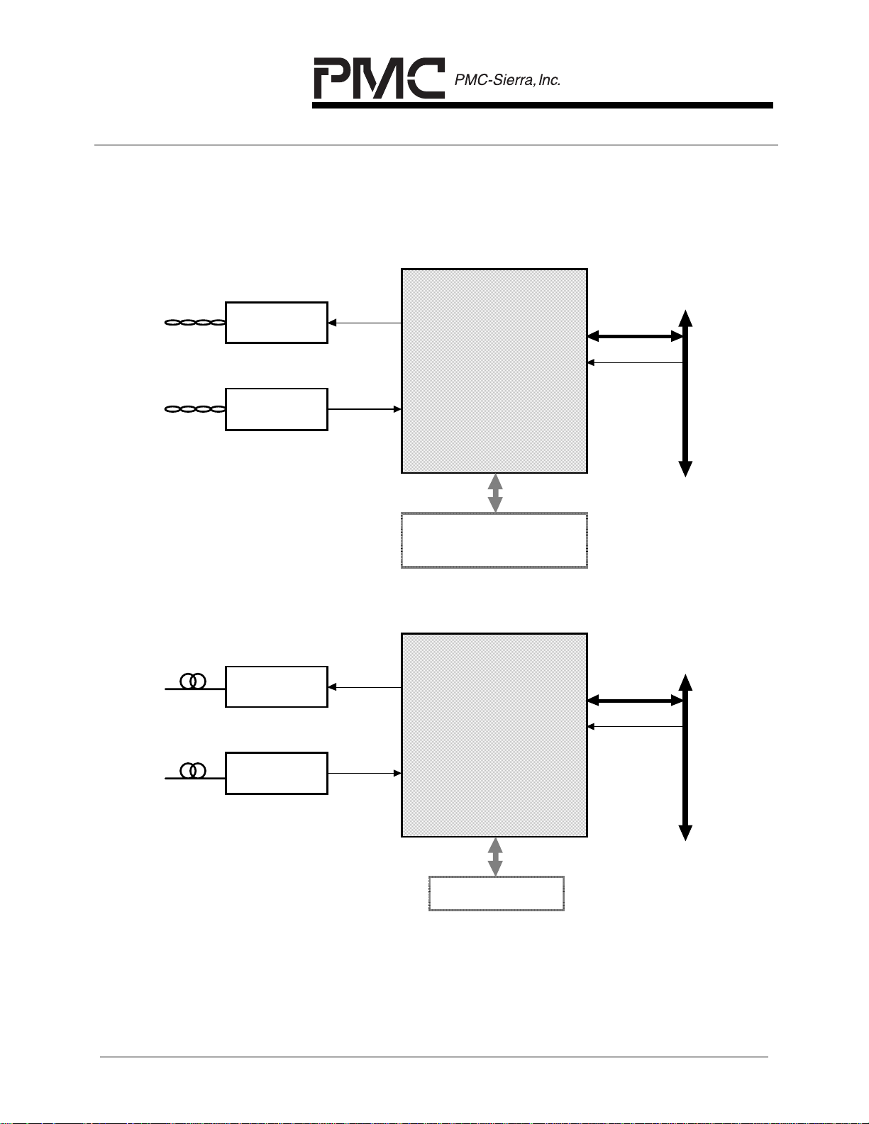
4.1.1.1 Fig. 4.1 Typical Applications
4.1.2 STS-3c UTP-5 ATM Operation
PCI
BUS
Line Driver
&
Transformer
UTP-5
Facility
Transformer,
Equalizer &
Line Receiver
TXD+/-
RXD+/-
PM7375
LASAR-155
AD[31:0]
Control
4.1.3 STS-3c/1 Optical ATM Operation
Electrical
to
Optical
TXD+/-
Optics
Facility
Optical
to
Electrical
RXD+/-
Optional Local
Microcontroller
PM7375
LASAR-155
Optional EPROM
PCI
BUS
AD[31:0]
Control
PROPRIETARY AND CONFIDENTIAL TO PMC-SIERRA, INC., AND FOR ITS CUSTOMERS’ INTERNAL USE
5
Page 22
PM7375 LASAR-155
DATA SHEET
PMC-931127 ISSUE 6 LOCAL ATM SAR & PHYSICAL LAYER
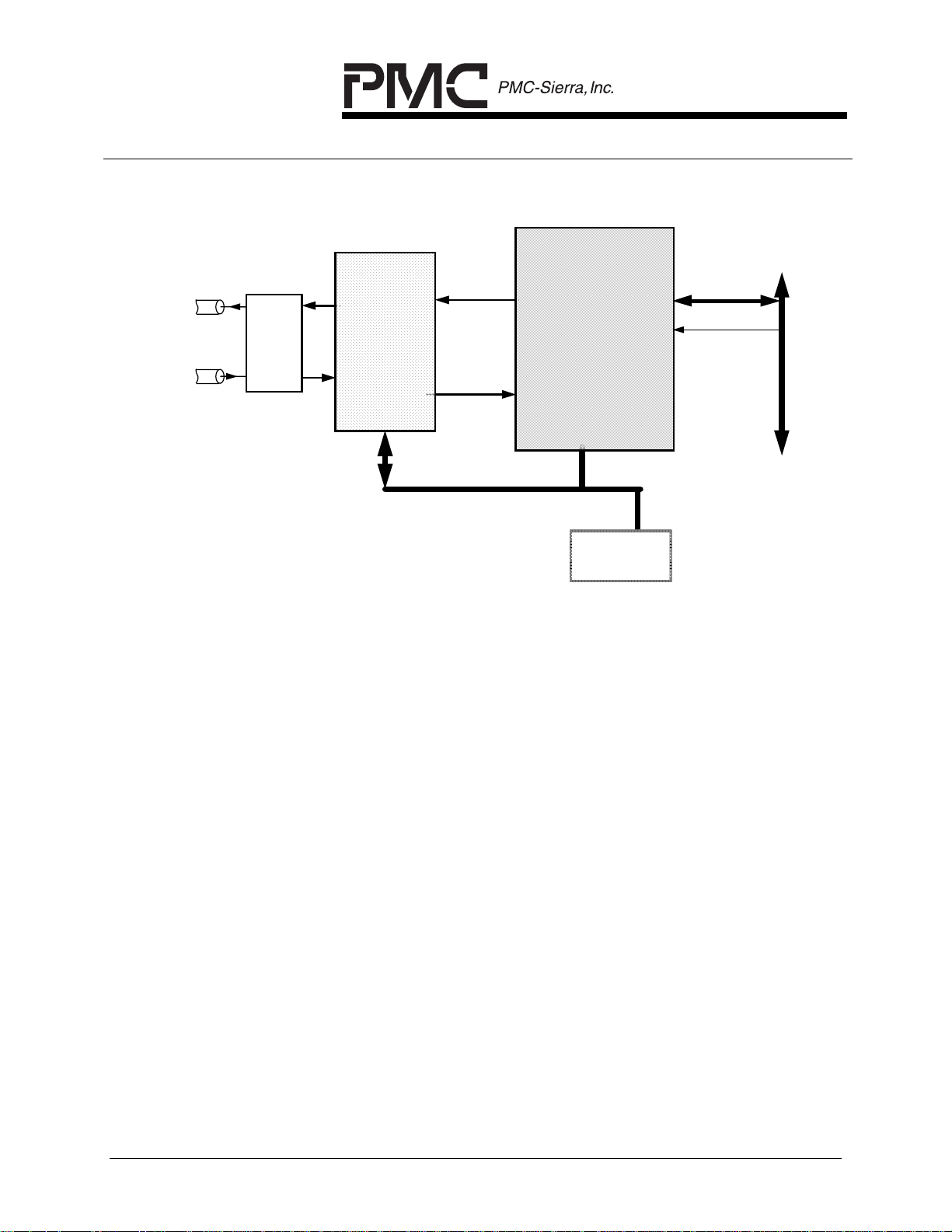
4.1.4 DS3/E3 ATM Operation
PCI
BUS
TDAT[7:0]
AD[31:0]
75 OHM
COAX
DS3/E3
LIU
PM7345
S/UNI-PDH
RDAT[7:0]
LASAR-155 LOCAL BUS
PM7375
LASAR-155
Optional
EPROM
Control
PROPRIETARY AND CONFIDENTIAL TO PMC-SIERRA, INC., AND FOR ITS CUSTOMERS’ INTERNAL USE
6
Page 23
PM7375 LASAR-155
DATA SHEET
PMC-931127 ISSUE 6 LOCAL ATM SAR & PHYSICAL LAYER
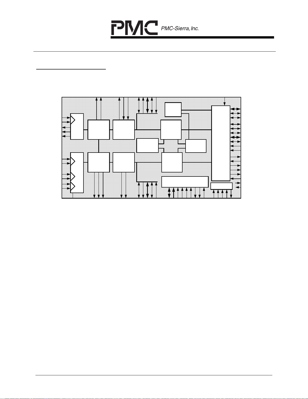
5
BLOCK DIAGRAM
TRCLK+
TRCLK-
TXC
TXD+
TXD-
RXD+
RXD-
RRCLK+
RRCLK-
ALOS+
ALOS-
Tx Line
I/F
Rx Line
I/F
LF+,LF-,LFO
TFPO
TCLK
Tx
Framer &
Overhead
Processor
Rx
Framer &
Overhead
Processor
RCLK
RALM
Tx ATM Cell
Rx ATM Cell
RFP
TGFC/TLD
TCP/TLDCLK
Processor
Processor
RGFC/RLD
RCP/RLDCLK
XOFF
TSOC
TWRENB
TDAT[7:0]
TXPHYBP
SAR
Performance
Monitor
RSOC
RRDENB
RDAT[7:0]
RXPHYBP
TFIFOFB/
TFIFOEB
Tx ATM
Traffic
Shaper
Tx ATM &
Adaptation
Layer
Processor
Rx ATM &
Adaptation
Layer
Processor
RFIFOFB
RFIFOEB/
Connection
Parameter
Microprocessor
I/F
ALE
CSB
WRB
A[8:0]
D[15:0]
Store
RDB
INTB
RSTB
MPENB
ROMP
PCI
DMA
Controller
JTAG Port
TCK
TMS
TRSTB
TDI
AD[31:0]
C/BEB[3:0]
PAR
FRAMEB
TRDYB
IRDYB
STOPB
DEVSELB
IDSEL
LOCKB
REQB
GNTB
PERRB
SERRB
PCIINTB
PCICLK
PCICLKO
SYSCLK
TDO
Normal Operating Mode (Slave Operation)
PROPRIETARY AND CONFIDENTIAL TO PMC-SIERRA, INC., AND FOR ITS CUSTOMERS’ INTERNAL USE
7
Page 24
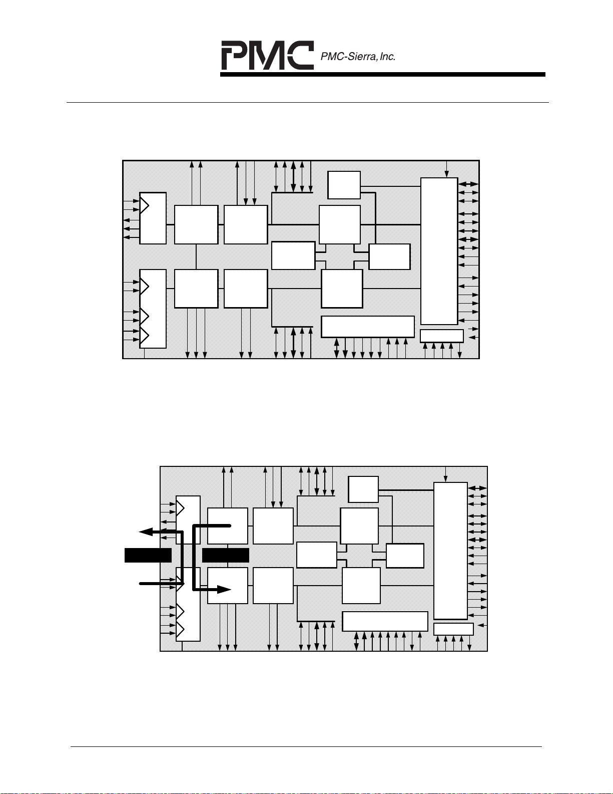
PM7375 LASAR-155
DATA SHEET
PMC-931127 ISSUE 6 LOCAL ATM SAR & PHYSICAL LAYER
TFPO
TCLK
TGFC/TLD
TCP/TLDCLK
XOFF
TSOC
TWRENB
TXPHYBP
TRCLK+
TRCLK-
TXC
TXD+
TXD-
RXD+
RXD-
RRCLK+
Tx Line
I/F
Rx Line
I/F
Tx
Framer &
Overhead
Processor
Rx
Framer &
Overhead
Processor
Tx ATM Cell
Processor
Rx ATM Cell
Processor
SAR
Performance
Monitor
RRCLK-
ALOS+
ALOS-
RFP
RCLK
LF+,LF-,LFO
RALM
RGFC/RLD
RCP/RLDCLK
RSOC
RRDENB
RXPHYBP
Normal Operating Mode ( Master Operation)
TFIFOFB/
TFIFOEB
TDAT[7:0]
Tx ATM &
Adaptation
Processor
Rx ATM &
Adaptation
Processor
RFIFOFB
RFIFOEB/
RDAT[7:0]
Tx ATM
Traffic
Shaper
Layer
Layer
Microprocessor
CS2B
D[7:0]
A[15:0]
Connection
Parameter
Store
I/F
RDB
WRB
CS1B
INTB
RSTB
MPENB
ROMP
PCI
DMA
Controller
JTAG Port
TCK
TMS
TRSTB
TDI
AD[31:0]
C/BEB[3:0]
PAR
FRAMEB
TRDYB
IRDYB
STOPB
DEVSELB
IDSEL
LOCKB
REQB
GNTB
PERRB
SERRB
PCIINTB
PCICLK
PCICLKO
SYSCLK
TDO
LINE
LOOPBACK
Loopback Modes
PROPRIETARY AND CONFIDENTIAL TO PMC-SIERRA, INC., AND FOR ITS CUSTOMERS’ INTERNAL USE
Tx Line
I/F
Rx Line
I/F
Tx
Framer &
Overhead
Processor
DIAGNOSTIC
LOOPBACK
Rx
Framer &
Overhead
Processor
Tx ATM Cell
Processor
Rx ATM Cell
Processor
SAR
Performance
Monitor
Tx ATM
Traffic
Shaper
Tx ATM &
Adaptation
Layer
Processor
Rx ATM &
Adaptation
Layer
Processor
Microprocessor
Connection
Parameter
Store
I/F
PCI
DMA
Controller
JTAG Port
8
Page 25

PM7375 LASAR-155
DATA SHEET
PMC-931127 ISSUE 6 LOCAL ATM SAR & PHYSICAL LAYER
6
DESCRIPTION
The PM7375 LASAR-155 Local ATM Segmentation and Reassembly & Physical
Layer device is a monolithic integrated circuit that implements SONET/SDH
transmission convergence, ATM cell mapping, ATM Adaptation Layer, and PCI Bus
memory management functions for a 155.52 or 51.84 Mbit/s ATM User Network
Interface.
The LASAR-155 receives SONET/SDH frames via a bit serial interface, recovers
clock and data, and processes section, line, and path overheads. It performs
framing (A1, A2), descrambling, detects alarm conditions, and monitors section, line,
and path bit interleaved parity (B1, B2, B3), accumulating error counts at each level
for performance monitoring purposes. Line and path far end block error indications
(Z2, G1) are also accumulated. The LASAR-155 interprets the received payload
pointers (H1, H2) and extracts the synchronous payload envelope which carries the
received ATM cell payload.
The LASAR-155 frames to the ATM payload using cell delineation. Payload
descrambling, HEC single bit error correction, cell filtering based on HEC errors and
idle/unassigned cell filtering is provided. The Generic Flow Control (GFC) field is
extracted from all received cell headers and serialized out a dedicated port. Counts
of received ATM cell headers that are in error and uncorrectable, cell headers that
are errored and correctable and all passed cells are accumulated independently for
performance monitoring purposes.
The LASAR-155 supports the simultaneous reassembly and Common Part
Convergence Sublayer (CPCS) processing for 128 open Virtual Circuits (VCs). All
receive VC parameters are stored locally in the LASAR-155 device to reduce
overhead traffic on the PCI Host bus. The LASAR-155 takes all received error free
cells and passes or blocks the cell based on an open VC. Passed cells are treated
as management, control or user cells. Management and control cell payloads are
optionally checked with a CRC-10 polynomial and are optionally DMA'd to receive
ready queues in packet memory.
User cells are associated with an open VC and DMA'd to reassembly queues in
packet memory. Once a packet is reassembled and verified using a CRC-32
polynomial, the entire packet is linked into a receive ready queue. The LASAR-155
alerts the PCI Host that there are reassembled packets or cells in a receive ready
queue by asserting an interrupt on the PCI bus.
All transmit VC parameters are stored in an internal transmit parameter table to
reduce overhead traffic on the PCI bus. After a PCI Host sets up a connection using
the transmit parameter table, the PCI Host can provide packets to transmit using a
PROPRIETARY AND CONFIDENTIAL TO PMC-SIERRA, INC., AND FOR ITS CUSTOMERS’ INTERNAL USE
9
Page 26

PM7375 LASAR-155
DATA SHEET
PMC-931127 ISSUE 6 LOCAL ATM SAR & PHYSICAL LAYER
high or low priority ready queue. The LASAR-155 automatically appends the AAL-5
trailer, segments the packet and subjects the cells to either peak cell rate or
sustainable cell rate enforcement.
The LASAR-155 generates most of a cell's header using the transmit parameter
table. The generic flow control (GFC) bits may optionally be inserted using a
dedicated serial port. The header error code (HEC) is automatically calculated and
inserted. The cell payload is optionally scrambled. Generated transmit cells are
automatically inserted into a STS-3c (STM-1) or STS-1 SONET/SDH Synchronous
Payload Envelope (SPE). In the absence of transmit cells, the LASAR-155
automatically inserts Idle/unassigned cells into the SPE.
The LASAR-155 transmits SONET/SDH frames, via a bit serial interface, and
formats SONET section, line, and path overhead appropriately. It performs framing
pattern insertion (A1, A2), scrambling, alarm signal insertion, and creates section,
line, and path bit interleaved parity (B1, B2, B3) as required to allow performance
monitoring at the far end. Line and path far end block error indications (Z2, G1) are
also inserted. The LASAR-155 generates the payload pointer (H1, H2) and inserts
the synchronous payload envelope which carries the ATM cell payload.
For system diagnostics, the LASAR-155 supports the insertion of a variety of errors
into the transmit stream, such as framing pattern errors, bit interleaved parity errors
and illegal pointers.
No auxiliary line clocks are required directly by the LASAR-155 as it is capable of
synthesizing the line rate transmit clock and recovering the receive clock
either a 19.44 MHz or 6.48 MHz reference clock
. The LASAR-155 is configured,
using
controlled and monitored via either the generic microprocessor port interface in
slave mode or the PCI bus interface in master mode. In slave mode, a mailbox
scheme with shared buffers is provided for communication between the
microprocessor and PCI Host.
The LASAR-155 can interface with external devices when the generic
microprocessor port interface is configured for master mode operation. In this mode
the PCI Host configures, controls and monitors the LASAR-155 and the external
devices.
The LASAR-155 is implemented in low power, 0.6 micron, +5 Volt CMOS
technology. It has TTL and pseudo ECL (PECL) compatible inputs and outputs and
is packaged in a 208 pin copper slugged plastic QFP package.
PROPRIETARY AND CONFIDENTIAL TO PMC-SIERRA, INC., AND FOR ITS CUSTOMERS’ INTERNAL USE
10
Page 27
PM7375 LASAR-155
DATA SHEET
PMC-931127 ISSUE 6 LOCAL ATM SAR & PHYSICAL LAYER
7
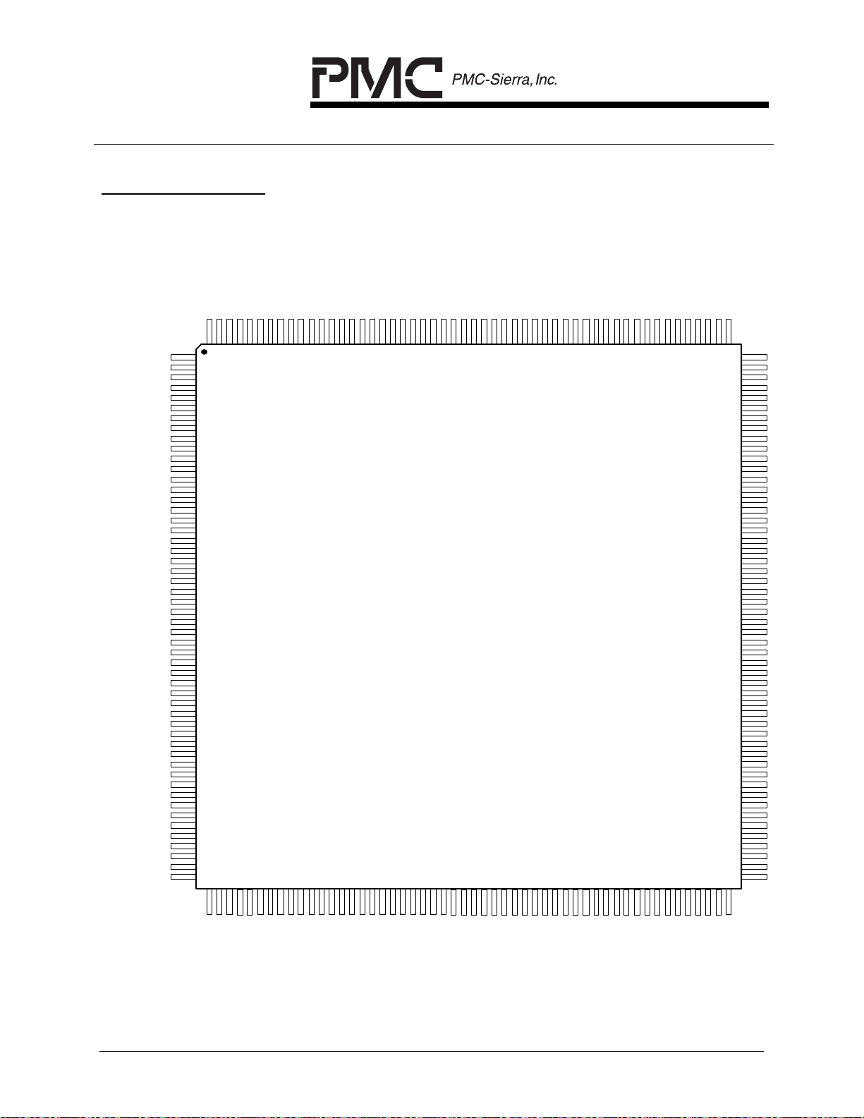
PIN DIAGRAM
The LASAR-155 is packaged in a 208 pin slugged plastic QFP package having a
body size of 28 mm by 28 mm and a pin pitch of 0.5 mm.
PIN 1
AD[27]
AD[26]
VSS_AC
VDD_AC
AD[25]
AD[24]
C/BEB[3]
VSS_AC
VSS_DC
VDD_DC
VDD_AC
IDSEL
AD[23]
AD[22]
AD[21]
VSS_AC
VDD_AC
AD[20]
AD[19]
AD[18]
VSS_AC
VDD_AC
AD[17]
AD[16]
C/BEB[2]
VSS_AC
VSS_DC
VDD_DC
FRAMEB
IRDYB
TRDYB
DEVSELB
STOPB
LOCKB
PERRB
SERRB
PAR
VDD_AC
C/BEB[1]
AD[15]
AD[14]
VSS_AC
VDD_AC
AD[13]
AD[12]
AD[11]
VSS_AC
VDD_AC
AD[10]
AD[9]
AD[8]
VSS_AC
PIN 52
VDD_AC
AD[28]
PIN 208
Index
VSS_AC
AD[30]
AD[29]
AD[31]
VDD_AC
REQB
GNTB
VSS_DC
VDD_DC
PCICLK
D[15]/A[15]
PCICLKO
PCIINTB
D[13]/A[13]
D[14]/A[14]
D[12]/A[12]
D[10]/A[10]
D[11]/A[11]
VSS_AC
A[8]
VSS_DC
VDD_DC
A[7]
D[9]/A[9]
A[6]
VDD_AC
PM7375
LASAR-155
TOP VIEW
A[5]
A[4]
A[3]
A[2]
A[1]
A[0]
D[8]
D[7]
D[6]
D[5]
D[4]
D[3]
D[2]
D[1]
VSS_DC
VDD_DC
D[0]
WRB
RDB
ALE/CS2B
CSB/CS1B
INTB
TFPO
RALM
PIN 157
PIN 156
VSS_DC
TCLK
VDD_DC
MPENB
RXPHYBP
RAVS1
RAVD2
LF+
LFLFO
RAVS2
RAVD1
RAVS4
RRCLKRRCLK+
RAVD4
RAVD3
ALOSALOS+
RXDRXD+
RAVS3
VSS_AC
VDD_AC
ROMP
VSS_DC
VSS_DC
VDD_DC
TXVSS
TXDTXD+
TXC
RSTB
TXVDD
TAVS3
TRCLKTRCLK+
TAVD3
TAVS2
TAVD2
TAVS1
TAVD1
XOFF
TGFC/TLD
TCP/TLDCLK
RGFC/RLD
RCP/RLDCLK
RFP
RRDENB
RSOC
RDAT[0]
RDAT[1]
PIN 105
TDI
TCK
TMS
VSS_DC
VDD_DC
PIN 53
AD[7]
C/BEB[0]
VDD_AC
AD[6]
VSS_AC
AD[5]
AD[4]
VDD_AC
AD[3]
VSS_AC
VDD_AC
AD[1]
AD[2]
AD[0]
VSS_AC
TDO
TRSTB
TDAT[7]
TDAT[6]
VSS_AC
VSS_DC
TFIFOFB/TFIFOEB
SYSCLK
VDD_DC
VDD_AC
TDAT[5]
TDAT[4]
VSS_DC
TDAT[1]
TDAT[2]
TDAT[3]
TSOC
TDAT[0]
TWRENB
RCLK
VSS_DC
VSS_AC
TXPHYBP
RFIFOEB/RFIFOFB
PROPRIETARY AND CONFIDENTIAL TO PMC-SIERRA, INC., AND FOR ITS CUSTOMERS’ INTERNAL USE
RDAT[7]
VDD_DC
VDD_AC
11
RDAT[5]
RDAT[4]
RDAT[6]
RDAT[2]
RDAT[3]
PIN 104
Page 28

PM7375 LASAR-155
DATA SHEET
PMC-931127 ISSUE 6 LOCAL ATM SAR & PHYSICAL LAYER
8
PIN DESCRIPTION (TOTAL 208)
8.1 Line Side Interface Signals (24)
Pin
Name
RXD+
RXD-
Type
PECL
Input
Pin
No.
136
137
Feature
The receive differential data inputs (RXD+, RXD-)
contain the 155.52 Mbit/s receive STS-3c (STM-1)
stream or the 51.84 Mbit/s receive STS-1 stream.
RXD+/- are sampled on the rising edge of RRCLK+/when clock recovery is disabled (the falling edge may
be used by reversing RRCLK+/-), otherwise the
receive clocks are recovered from the RXD+/- bit
stream. RXD+/- is expected to be NRZ encoded.
RRCLK+
RRCLK-
PECL
Input
142
143
The receive differential reference clock inputs
(RRCLK+, RRCLK-) contain a jitter-free 1 9.44 MHz or
6.48 MHz reference clock when clock recovery is
enabled. When clock recovery is bypassed, RRCLK+/is nominally a 155.52 MHz or 51.84 MHz, 50% duty
cycle clock and provide timing for the LASAR-155
receive functions. In this case, RXD+/- is sampled on
the rising edge of RRCLK+/-.
Clock recovery bypass is selectable using the RBYP
bit in the LASAR-155 Master Configuration register.
ALOS+
ALOS-
PECL
Input
138
139
The analog loss of signal (ALOS+/-) differential inputs
are used to indicate a loss of receive signal power.
When ALOS+/- is asserted, the data on the receive
data (RXD+/-) pin will be squelched and the phase
locked loop shall switch to the reference clock
(RRCLK+/-) to keep the recovered clock in range.
These inputs must be DC coupled.
LF+,
LF-,
LFO
Analog 149
148
147
Passive components connected to the recovery loop
filter (LF+, LF- and LFO) pins determine the dynamics
of the clock recovery unit. Refer to the Operation
section for details.
PROPRIETARY AND CONFIDENTIAL TO PMC-SIERRA, INC., AND FOR ITS CUSTOMERS’ INTERNAL USE
12
Page 29

PM7375 LASAR-155
DATA SHEET
PMC-931127 ISSUE 6 LOCAL ATM SAR & PHYSICAL LAYER
RCLK Output 96 The receive clock (RCLK) output provides a timing
reference for the LASAR-155 receive line interface
outputs. RCLK is a 19.44 MHz or 6.48 MHz, nominally
50% duty cycle clock. RCLK is a divide by eight of the
recovered clock or the RRCLK+/- inputs as
determined using the RBYP bit in the LASAR-155
Master Configuration register.
RALM Output 157 The receive alarm (RALM) output indicates the state
of the receive framing. RALM is low if no receive
alarms are active. RALM is high if loss of signal
(LOS), line AIS, path AIS, loss of frame (LOF), loss of
pointer (LOP) or loss of cell delineation (LCD) is
detected. RALM is updated on the falling edge of
RCLK.
RFP Output 109 The receive frame pulse (RFP) output is an 8 kHz
signal derived from the receive line clock. RFP is
pulsed high for one RCLK cycle every 2430 RCLK
cycles for STS-3c (STM-1) or every 810 RCLK cycles
for STS-1. A single discontinuity in RFP position
occurs if a change of frame alignment occurs.
TRCLK+
TRCLK-
PECL
Input
120
121
The transmit differential reference clock inputs
(TRCLK+, TRCLK-) are a jitter-free 19.44 MHz or 6.48
MHz reference clock when clock synthesis is enabled.
When clock synthesis is bypassed, TRCLK+/- is
nominally a 155.52 MHz or 51.84 MHz, 50% duty
cycle clock. This clock provides timing for the
LASAR-155 transmit functions. TRCLK+/- may be left
unconnected when LASAR-155 loop timing is enabled
using the LASAR-155 Master Control Register.
TXC Output 125 The transmit clock (TXC) output is available when
STS-1 (51.84 Mbits/s) mode of operation is selected
using the LASAR-155 Master Configuration register.
When STS-3c (STM-1) mode of operation is selected,
TXC is held low. TXD+/- are updated on the falling
edge of TXC.
PROPRIETARY AND CONFIDENTIAL TO PMC-SIERRA, INC., AND FOR ITS CUSTOMERS’ INTERNAL USE
13
Page 30

PM7375 LASAR-155
DATA SHEET
PMC-931127 ISSUE 6 LOCAL ATM SAR & PHYSICAL LAYER
TXD+
TXD-
Output 126
127
The transmit differential data outputs (TXD+, TXD-)
contain the 155.52 Mbit/s transmit STS-3c (STM-1)
stream or the 51.84 Mbit/s transmit STS-1 stream.
When the STS-1 stream is selected, TXD+/- are
updated on the falling edge of TXC. TXD+/- is NRZ
encoded.
TCLK Output 155 The transmit byte clock (TCLK) is either a 19.44 MHz
or a 6.48 MHz clock derived from the transmit line
rate.
TFPO Output 158 The active high framing position output (TFPO) signal
is an 8 kHz timing marker for the transmitter. TFPO
goes high for a single TCLK period once every 2430 in
STS-3c (STM-1) mode or 810 in STS-1 mode TCLK
cycles. TFPO is updated on the rising edge of TCLK.
RGFC/RLD Output 111 The RGFC/RLD output is a dual function output
controlled using the UNI_POTS bit in the LASAR-155
Master Configuration register.
When the UNI_POTS bit is low, the receive generic
flow control (RGFC) output presents the extracted GFC
bits in a serial stream. The four GFC bits are
presented for each received cell, with the RCP output
indicating the position of the most significant bit. The
updating of RGFC by particular GFC bits may be
disabled through the RACP Configuration register. The
serial link is forced low if cell delineation is lost. RGFC
is updated on the rising edge of RCLK.
When the UNI_POTS bit is high, the receive line DCC
(RLD) signal contains the serial line data
communications channel (D4 - D12) extracted from the
incoming stream. RLD is updated on the falling edge
of RLDCLK.
PROPRIETARY AND CONFIDENTIAL TO PMC-SIERRA, INC., AND FOR ITS CUSTOMERS’ INTERNAL USE
14
Page 31

PM7375 LASAR-155
DATA SHEET
PMC-931127 ISSUE 6 LOCAL ATM SAR & PHYSICAL LAYER
RCP/
RLDCLK
Output 110 The RCP/RLDCLK output is a dual function output
controlled using the UNI_POTS bit in the LASAR-155
Master Configuration register.
When the UNI_POTS bit is low, the receive cell pulse
(RCP) indicates the location of the four GFC bits in the
RGFC serial stream. RCP is coincident with the most
significant GFC bit. RCP is updated on the rising edge
of RCLK.
When the UNI_POTS bit is high, the receive line DCC
clock (RLDCLK) is a 576 kHz clock used to update the
RLD output. RLDCLK is generated by gapping a
2.16 MHz clock.
TGFC/TLD Input 113 The TGFC/TLD input is a dual function input controlled
using the UNI_POTS bit in the LASAR-155 Master
Configuration register.
When the UNI_POTS bit is low, the transmit generic
flow control (TGFC) input provides the ability to insert
the GFC value. The four TCLK periods following the
TCP output pulse contain the GFC value to be
inserted into the current cell. The GFC enable bits of
the TACP Configuration register enable the insertion of
each serial bit. TGFC is sampled on the rising edge of
TCLK.
When the UNI_POTS bit is high, the transmit line
DCC (TLD) signal contains the serial line data
communications channel (D4 - D12). TLD is sampled
on the rising edge of TLDCLK.
PROPRIETARY AND CONFIDENTIAL TO PMC-SIERRA, INC., AND FOR ITS CUSTOMERS’ INTERNAL USE
15
Page 32

PM7375 LASAR-155
DATA SHEET
PMC-931127 ISSUE 6 LOCAL ATM SAR & PHYSICAL LAYER
TCP/
TLDCLK
Output 112 The TGFC/TLDCLK output is a dual function output
controlled using the UNI_POTS bit in the LASAR-155
Master Configuration register.
When the UNI_POTS bit is low, the transmit cell pulse
(TCP) indicates where the valid TGFC serial bits are
expected. If TCP is asserted high, the most significant
GFC bit is expected in the subsequent TCLK period.
TCP pulses high for one TCLK for every transmitted
cell. TCP is updated on the rising edge of TCLK.
When the UNI_POTS bit is high, the transmit line DCC
clock (TLDCLK) is a 576 kHz clock used to sample the
TLD input. TLDCLK is generated by gapping a
2.16 MHz clock.
XOFF Input 114 The transmit off (XOFF) signal can be used to control
the transmission of user cells. When XOFF is asserted
high, the LASAR-155 is prohibited from transmitting
user cells. Under this operating condition, the
LASAR-155 can only transmit Idle/Unassigned cells.
When XOFF is low, the LASAR-155 operates normally.
XOFF is sampled on the rising edge of TCLK.
PROPRIETARY AND CONFIDENTIAL TO PMC-SIERRA, INC., AND FOR ITS CUSTOMERS’ INTERNAL USE
16
Page 33

PM7375 LASAR-155
DATA SHEET
PMC-931127 ISSUE 6 LOCAL ATM SAR & PHYSICAL LAYER
8.2 Multipurpose Port Interface Signals (24)
Pin
Name
Type
Pin
No.
Feature
RXPHYBP I/O 152 The receive physical layer bypass (RXPHYBP) signal
selects whether or not to bypass the internal SONET
PHY in the receive direction. When RXPHYBP is set
high, the internal SONET PHY is bypassed and a SCIPHY/Utopia compliant interface consisting of signals:
RSOC, RRDENB, RFIFOEB and RDAT[7:0] is
supported. When RXPHYBP is set low, the
LASAR-155 operates normally with the internal
SONET PHY. In this mode, signals RSOC, RRDENB,
RFIFOFB and RDAT[7:0] can be used to interface to
an external FIFO to support CBR VCs and
Management cells.
Under analog test mode as selected using the
PMCATST bit in the LASAR-155 Master Test register,
this pin is configured as an output and is used for test
purposes.
PROPRIETARY AND CONFIDENTIAL TO PMC-SIERRA, INC., AND FOR ITS CUSTOMERS’ INTERNAL USE
17
Page 34

PM7375 LASAR-155
DATA SHEET
PMC-931127 ISSUE 6 LOCAL ATM SAR & PHYSICAL LAYER
RRDENB Output 108 The active low receive read enable (RRDENB) signal's
function is configured using input RXPHYBP.
When RXPHYBP is set high, the LASAR-155's
SONET physical layer blocks are bypassed and
RRDENB is used to initiate reads from an external
FIFO associated with a physical layer device (eg. the
PMC SUNI-PDH device). When RRDENB is set low
and RFIFOEB is sampled high on a rising edge of
SYSCLK, a cell byte is sampled on the RDAT[7:0] bus
on the next rising edge of SYSCLK. If RRDENB is set
high on the rising edge of SYSCLK, a cell byte is not
sampled on the next rising edge of SYSCLK.
RRDENB is updated on the rising edge of SYSCLK.
When RXPHYBP is set low, the LASAR-155 operates
normally with the integrated STS-3c (STM-1) or STS-1
PHY. When RRDENB is set low on the rising edge of
SYSCLK, the data on the RDAT[7:0] bus is valid. When
RRDENB is set high on the rising edge of SYSCLK,
the data on the RDAT[7:0] bus is not valid. RRDENB
is updated on the rising edge of SYSCLK.
RSOC I/O 107 The receive start of cell (RSOC) signal's function is
configured using input RXPHYBP.
When RXPHYBP is set high, RSOC becomes an input
and is expected to mark the start of cell on the
RDAT[7:0] bus. For this mode of operation, RSOC is
sampled using the rising edge of SYSCLK.
When RXPHYBP is set low, RSOC becomes an output
and marks the start of cell on the RDAT[7:0] bus. For
this mode of operation, RSOC is updated on the rising
edge of SYSCLK.
PROPRIETARY AND CONFIDENTIAL TO PMC-SIERRA, INC., AND FOR ITS CUSTOMERS’ INTERNAL USE
18
Page 35

PM7375 LASAR-155
DATA SHEET
PMC-931127 ISSUE 6 LOCAL ATM SAR & PHYSICAL LAYER
RDAT[0]
RDAT[1]
RDAT[2]
RDAT[3]
RDAT[4]
RDAT[5]
RDAT[6]
RDAT[7]
RFIFOEB
I/O 106
105
104
103
102
101
100
99
The receive cell data (RDAT[7:0]) bus' function is
configured using input RXPHYBP.
When RXPHYBP is set high, the RDAT[7:0] signals
become inputs and are expected to carry the ATM cell
octets that are read from an external FIFO associated
with an external physical layer device. For this mode
of operation, RDAT[7:0] is sampled using the rising
edge of SYSCLK.
When RXPHYBP is set low, the RDAT[7:0] signals
become outputs and carry ATM cell octets marked for
this output port. For this mode of operation,
RDAT[7:0] is updated on the rising edge of SYSCLK.
Input 93 When RXPHYBP is set high, the active low receive
FIFO empty (RFIFOEB) signal indicates when a byte is
available to be read from an external FIFO. When
sampled high, RFIFOEB indicates that at least one
byte can be read. When sampled low, RFIFOEB
indicates that there are no bytes to be read. In this
mode of operation, RFIFOEB is sampled using the
rising edge of SYSCLK.
RFIFOFB
When RXPHYBP is set low, the active low receive
FIFO full (RFIFOFB) signal indicates when a byte can
be written to an external FIFO. When sampled high,
RFIFOFB indicates that at least one byte can be
written. When sampled low, RFIFOFB indicates that
the external FIFO is full and can accept no more
writes. In this mode of operation, RFIFOFB is
sampled using the rising edge of SYSCLK.
PROPRIETARY AND CONFIDENTIAL TO PMC-SIERRA, INC., AND FOR ITS CUSTOMERS’ INTERNAL USE
19
Page 36

PM7375 LASAR-155
DATA SHEET
PMC-931127 ISSUE 6 LOCAL ATM SAR & PHYSICAL LAYER
TXPHYBP I/O 92 The transmit physical layer bypass (TXPHYBP) signal
selects whether or not to bypass the internal SONET
PHY in the transmit direction. When TXPHYBP is set
high, the internal SONET PHY is bypassed and a SCIPHY/Utopia compliant interface comprising of signals:
TSOC, TWRENB , TFIFOFB and TDAT[7:0] is
supported. When TXPHYBP is set low, the
LASAR-155 operates normally with the internal
SONET PHY. In this mode, signals TSOC, TWRENB,
TFIFOEB and TDAT[7:0] can be used to interface to
an external FIFO to support CBR VCs.
Under analog test mode as selected using the
PMCATST bit in the LASAR-155 Master Test register,
this pin is configured as an output and is used for test
purposes.
TWRENB Output 91 The active low transmit write enable (TWRENB)
signal's function is configured using input TXPHYBP.
When TXPHYBP is set high, the LASAR-155's
SONET physical layer blocks are bypassed and
TWRENB is used to initiate writes to a n external FIFO
associated with a physical layer device (e.g. the PMC
SUNI-PDH). When TWRENB is low and TFIFOFB is
high during a SYSCLK cycle, the current cell byte on
bus TDAT[7:0] is written into the external FIFO. When
TWRENB is high during a SYSCLK cycle, no write is
performed. In this mode of operation, TWRENB is
generated using the rising edge of SYSCLK.
When TXPHYBP is set low, the LASAR-155 operates
normally with the integrated STS-3c (STM-1) or STS-1
PHY. When TWRENB is low on the rising edge of a
SYSCLK cycle and TFIFOEB is high, a cell byte is
expected on the TDAT[7:0] bus on the next rising edge
of SYSCLK. When TWRENB is set high on the rising
edge of a SYSCLK cycle, data is not expected on the
TDAT[7:0] bus on the next rising edge of SYSCLK.
Once a full cell is sampled, it is automatically insert ed
into the cell stream. In this mode of operation,
TWRENB is generated using the rising edge of
SYSCLK.
PROPRIETARY AND CONFIDENTIAL TO PMC-SIERRA, INC., AND FOR ITS CUSTOMERS’ INTERNAL USE
20
Page 37

PM7375 LASAR-155
DATA SHEET
PMC-931127 ISSUE 6 LOCAL ATM SAR & PHYSICAL LAYER
TSOC I/O 90 The transmit start of cell (TSOC) signal's function is
configured using input TXPHYBP.
When TXPHYBP is set high, TSOC becomes an output
and is expected to mark the start of cell on the
TDAT[7:0] bus. For this mode of operation, TSOC is
updated on the rising edge of SYSCLK.
When TXPHYBP is set low, TSOC becomes an input
and marks the start of cell on the TDAT[7:0] bus. When
TSOC is high, the first octet of the cell is present on
the TDAT[7:0] bus. It is not necessary for TSOC to be
present at each cell. An interrupt may be generated if
TSOC is high during any word other than the first word
of the selected data structure. For this mode of
operation, TSOC is sampled using the rising edge of
SYSCLK.
TDAT[0]
TDAT[1]
TDAT[2]
TDAT[3]
TDAT[4]
TDAT[5]
TDAT[6]
TDAT[7]
I/O 89
88
87
86
85
84
77
76
The transmit cell data (TDAT[7:0]) bus' function is
configured using input TXPHYBP.
When TXPHYBP is set high, the TDAT[7:0] signals
become outputs and carry the ATM cell octets that are
written to a FIFO associated with an external physical
layer device. For this mode of operation, TDAT[7:0] is
updated on the rising edge of SYSCLK.
When TXPHYBP is set low, the TDAT[7:0] signals
become inputs and carry the ATM cell octets that are
read from an external FIFO. For this mode of
operation, TDAT[7:0] is sampled using the rising edge
of SYSCLK.
PROPRIETARY AND CONFIDENTIAL TO PMC-SIERRA, INC., AND FOR ITS CUSTOMERS’ INTERNAL USE
21
Page 38

PM7375 LASAR-155
DATA SHEET
PMC-931127 ISSUE 6 LOCAL ATM SAR & PHYSICAL LAYER
TFIFOFB
TFIFOEB
Input 75 When TXPHYBP is set high, the active low transmit
FIFO full (TFIFOFB) signal indicates when a byte can
be written to an external FIFO. When sampled low,
TFIFOFB indicates that the external FIFO is full and
can accept four more writes. When sampled high,
TFIFOFB indicates that at least one byte can be
written. In this mode of operation, TFIFOFB is
sampled using the rising edge of SYSCLK.
When TXPHYBP is set low, the active low transmit
FIFO empty (TFIFOEB) signal indicates when a byte is
available to be read from an external FIFO. When
sampled low, TFIFOEB indicates that there are no
bytes to be read. When sampled high, TFIFOEB
indicates that at least one byte can be read. In this
mode of operation, TFIFOEB is sampled using the
rising edge of SYSCLK.
PROPRIETARY AND CONFIDENTIAL TO PMC-SIERRA, INC., AND FOR ITS CUSTOMERS’ INTERNAL USE
22
Page 39

PM7375 LASAR-155
DATA SHEET
PMC-931127 ISSUE 6 LOCAL ATM SAR & PHYSICAL LAYER
8.3 PCI Host Interface Signals (52)
Pin
Name
Type
Pin
No.
Feature
PCICLK Input 198 The PCI clock (PCICLK) provides timing for PCI bus
accesses. PCICLK should be nominally a 50% duty
cycle 0 to 33 MHz clock.
PCICLKO Output 196 The PCI clock output (PCICLKO) is a buffered version
of the PCI clock input, PCICLK. PCICLKO can be used
to drive the SYSCLK input.
ROMP Input 132 The ROMP input can be used to indicate whether an
Expansion ROM is present or not. If ROMP is logic
one, an expansion ROM is assumed to be present on
the LASAR-155 local bus and the Expansion ROM
Base Address register operates normally. If ROMP is
logic zero, the XRBS bits in the Expansion ROM Base
Address register is zeroed out indicating there is no
expansion ROM. ROMP must be used to allow
Interoperability with some BIOs implementations.
ROMP has an integral pull up resistor.
PROPRIETARY AND CONFIDENTIAL TO PMC-SIERRA, INC., AND FOR ITS CUSTOMERS’ INTERNAL USE
23
Page 40

PM7375 LASAR-155
DATA SHEET
PMC-931127 ISSUE 6 LOCAL ATM SAR & PHYSICAL LAYER
AD[0]
AD[1]
AD[2]
AD[3]
AD[4]
AD[5]
AD[6]
AD[7]
AD[8]
AD[9]
AD[10]
AD[11]
AD[12]
AD[13]
AD[14]
AD[15]
AD[16]
AD[17]
AD[18]
AD[19]
AD[20]
AD[21]
AD[22]
AD[23]
AD[24]
AD[25]
AD[26]
AD[27]
AD[28]
AD[29]
AD[30]
AD[31]
I/O 68
67
66
63
62
61
58
57
51
50
49
46
45
44
41
40
24
23
20
19
18
15
14
13
6
5
2
1
208
205
204
203
The PCI address and data (AD[31:0]) bus is used to
carry multiplexed address and data. During the first
clock cycle of a transaction, AD[31:0] contains a
physical byte address. Subsequent clock cycles of a
transaction should contain data.
A transaction is defined as an address phase followed
by one or more data phases. When Little-Endian byte
formatting is used. AD[31:24] should contain the most
significant byte of a DWORD while AD[7:0] should
contain the least significant byte of a DWORD. When
Big-Endian byte formatting is used. AD[7:0] should
contain the most significant byte of a DWORD while
AD[31:24] should contain the least significant byte of a
DWORD.
When the LASAR-155 is the initiator, AD[31:0] are
outputs during the first (address) phase of a
transaction. For write transactions, AD[31:0] remain
outputs for the data phases of the transaction. For
read transactions, AD[31:0] become inputs.
When the LASAR-155 is the target, AD[31:0] are
inputs during the first (address) phase of a
transaction. For write transactions, AD[31:0] become
inputs for the data phases of the transaction. For read
transactions, AD[31:0] remain outputs for the
transaction.
When the LASAR-155 is not involved in the current
transaction, AD[31:0] are tri-stated.
Signals, AD[31:0] are updated on the rising edge of
PCICLK or sampled using the rising edge of PCICLK
depending on whether they are outputs or inputs.
PROPRIETARY AND CONFIDENTIAL TO PMC-SIERRA, INC., AND FOR ITS CUSTOMERS’ INTERNAL USE
24
Page 41

PM7375 LASAR-155
DATA SHEET
PMC-931127 ISSUE 6 LOCAL ATM SAR & PHYSICAL LAYER
C/BEB[0]
C/BEB[1]
C/BEB[2]
C/BEB[3]
I/O 56
39
25
7
The PCI bus command and byte enable (C/BEB[3:0])
bus contains the bus command or the byte valid
indications. During the first clock cycle of a
transaction, C/BEB[3:0] contains the bus command
code. For subsequent clock cycles, C/BEB[3:0]
identifies which bytes on the AD[31:0] bus carry
meaningful data. C/BEB[3] is associated with byte 3
(AD[31:24]) while C/BEB[0] is associated with byte 0
(AD[7:0]). When C/BEB[n] is high, the associated byte
is meaningless. When C/BEB[n] is low, the associated
byte is valid.
When the LASAR-155 is the initiator, C/BEB[3:0] are
outputs.
When the LASAR-155 is the target, C/BEB[3:0] are
inputs.
When the LASAR-155 is not involved in the current
transaction, C/BEB[3:0] are tri-stated.
C/BEB[3:0] are updated on the rising edge of PCICLK
or sampled using the rising edge of PCICLK
depending on whether they are outputs or inputs.
PAR I/O 37 The parity (PAR) signal is the even parity calculated
over the 36 signals, AD[31:0] and C/BEB[3:0]
regardless of whether all the bytes of the AD bus are
meaningful. PAR always is the calculated parity for the
previous PCICLK cycle. Parity errors detected by the
LASAR-155 are indicated on output PERRB and in the
PCID Interrupt Status register.
When the LASAR-155 is the initiator, PAR is an output
for writes and an input for reads.
When the LASAR-155 is the target, PAR is an input for
writes and an output for reads.
When the LASAR-155 is not involved in the current
transaction, PAR is tri-stated.
PAR is updated on the rising edge of PCICLK or
sampled using the rising edge of PCICLK depending
on whether it is an output or an input.
PROPRIETARY AND CONFIDENTIAL TO PMC-SIERRA, INC., AND FOR ITS CUSTOMERS’ INTERNAL USE
25
Page 42

PM7375 LASAR-155
DATA SHEET
PMC-931127 ISSUE 6 LOCAL ATM SAR & PHYSICAL LAYER
FRAMEB I/O 29 The active low cycle frame (FRAMEB) is used to
identify a transaction cycle. When FRAMEB
transitions low, the start of a bus transaction is
indicated. FRAMEB remains low to define the
duration of the cycle. When FRAMEB transitions high,
the last data phase of the current transaction is
indicated.
When the LASAR-155 is the initiator, FRAMEB is an
output.
When the LASAR-155 is the target, FRAMEB is an
input.
When the LASAR-155 is not involved in the current
transaction, FRAMEB is tri-stated.
FRAMEB is updated on the rising edge of PCICLK or
sampled using the rising edge of PCICLK depending
on whether it is an output or an input.
TRDYB I/O 31 The active low target ready (TRDYB) signal is used to
indicate whether the target is ready to start or continue
a transaction. TRDYB works in conjunction with
IRDYB to complete transaction data phases. When
TRDYB is high and a transaction is in progress, the
target could not complete the current data phase and
is forcing a wait state. When TRDYB is low and a
transaction is in progress, the target has completed
the current data phase. Note, whether the data phase
is completed or not depends on the initiator's ready
signal IRDYB.
When the LASAR-155 is the initiator, TRDYB is an
input.
When the LASAR-155 is the target, TRDYB is an
output. It is expected that for LASAR-155 register
accesses, TRDYB will be used to extend data phases
to multiple PCICLK cycles.
When the LASAR-155 is not involved in the current
transaction, TRDYB is tri-stated.
TRDYB is updated on the rising edge of PCICLK or
sampled using the rising edge of PCICLK depending
on whether it is an output or an input.
PROPRIETARY AND CONFIDENTIAL TO PMC-SIERRA, INC., AND FOR ITS CUSTOMERS’ INTERNAL USE
26
Page 43

PM7375 LASAR-155
DATA SHEET
PMC-931127 ISSUE 6 LOCAL ATM SAR & PHYSICAL LAYER
IRDYB I/O 30 The active low initiator ready (IRDYB) signal is used to
indicate whether the initiator is ready to start or
continue a transaction. IRDYB works in conjunction
with TRDYB to complete transaction data phases.
When IRDYB is high and a transaction is in progress,
the initiator could not complete the current data phase
and is forcing a wait state. When IRDYB is low and a
transaction is in progress, the initiator has completed
the current data phase. Note, whether the data phase
is completed or not depends on the target's ready
signal TRDYB.
When the LASAR-155 is the initiator, IRDYB is an
output.
When the LASAR-155 is the target, IRDYB is an input.
When the LASAR-155 is not involved in the current
transaction, IRDYB is tri-stated.
IRDYB is updated on the rising edge of PCICLK or
sampled using the rising edge of PCICLK depending
on whether it is an output or an input.
STOPB I/O 33 The active low stop (STOPB) signal is used by a target
to request the initiator to stop the current bus
transaction. When STOPB is high, the initiator
continues with the transaction. When STOPB is low,
the initiator should stop the current transaction.
When the LASAR-155 is the initiator, STOPB is an
input. If STOPB is sampled low, the LASAR-155
terminates the current transaction in the next PCICLK
cycle.
When the LASAR-155 is the target, STOPB is an
output. As a target, the LASAR-155 only issues
transaction stop requests when its internal bus latency
buffers are in a near overflow state.
When the LASAR-155 is not involved in the current
transaction, STOPB is tri-stated.
STOPB is updated on the rising edge of PCICLK or
sampled using the rising edge of PCICLK depending
on whether it is an output or an input.
PROPRIETARY AND CONFIDENTIAL TO PMC-SIERRA, INC., AND FOR ITS CUSTOMERS’ INTERNAL USE
27
Page 44

PM7375 LASAR-155
DATA SHEET
PMC-931127 ISSUE 6 LOCAL ATM SAR & PHYSICAL LAYER
IDSEL Input 12 The initialization device select (IDSEL) signal is used
as the chip select during PCI configuration register
reads and writes. When high during the address
phase of a transaction with the C/BEB[3:0] code
indicating a register read or write, the LASAR-155
assumes a PCI configuration register transaction. In
response, the LASAR-155 asserts the DEVSELB
signal in the subsequent PCICLK period.
IDSEL is sampled using the rising edge of PCICLK.
DEVSELB I/O 32 The device select (DEVSELB) signal is forced low by a
target to claim the current bus transaction. During the
address phase of a transaction, all targets decode the
address on the AD[31:0] bus. If a target recognizes
the address as its own, it forces DEVSELB low to
indicate to the initiator that the address is valid. If no
target claims the address in six bus clock cycles, the
initiator must assume that the target does not exist or
cannot respond and must abort the transaction.
When the LASAR-155 is the initiator, DEVSELB is an
input. If no target responds to an address in six
PCICLK cycles, the LASAR-155 aborts the current
transaction and alerts the PCI Host via an interrupt.
When the LASAR-155 is the target, DEVSELB is an
output.
DEVSELB is updated on the rising edge of PCICLK or
sampled using the rising edge of PCICLK depending
on whether it is an output or an input. When the
LASAR-155 is not involved in the current transaction,
DEVSELB is tri-stated.
LOCKB Input 34 The active low bus lock (LOCKB) signal is used to lock
a target device. When LOCKB is low, FRAMEB is low
and the LASAR-155 is the target, an initiator is locking
the LASAR-155 as an "owned" target. Under these
circumstances, the LASAR-155 will reject all
transaction with other initiators. The LASAR-155 will
continue to reject other initiators until its owner
releases the lock by forcing both FRAMEB and
LOCKB high. As an initiator, the LASAR-155 never
locks a target.
LOCKB is sampled using the rising edge of PCICLK.
PROPRIETARY AND CONFIDENTIAL TO PMC-SIERRA, INC., AND FOR ITS CUSTOMERS’ INTERNAL USE
28
Page 45

PM7375 LASAR-155
DATA SHEET
PMC-931127 ISSUE 6 LOCAL ATM SAR & PHYSICAL LAYER
REQB Output 201 The active low PCI bus request (REQB) signal is used
by the LASAR-155 to request an external arbiter for
control of the PCI bus. REQB is forced low when the
internal PCI DMA controller requires access to the
packet memory. Otherwise, REQB is forced high.
REQB is updated on the rising edge of PCICLK.
GNTB Input 200 The active low PCI bus grant (GNTB) signal is used to
grant control of the PCI to the LASAR-155 in response
to a bus request via the REQB output. When GNTB is
high, the LASAR-155 does not control the PCI bus
and thus must wait. When GNTB is low, the external
arbiter has granted the LASAR-155 control of the PCI
bus. However, the LASAR-155 does not proceed until
the FRAMEB signal is high indicating no current
transactions.
GNTB is sampled using the rising edge of PCICLK.
PERRB Output 35 The active low parity error (PERRB) signal indicates
when the LASAR-155 detects a parity error over the
AD[31:0] and C/BEB[3:0] signals when compared to
the PAR input. PERRB is high when no parity error is
detected. PERRB is forced low for the cycle
immediately following the offending PAR cycle.
PERRB is enabled using a bit in the Control register in
the PCI Configuration registers space. In addition,
regardless of whether output, PERRB is enabled or
not, parity errors are indicated in the Status register in
the PCI Configuration registers space.
PERRB is updated on the rising edge of PCICLK.
PROPRIETARY AND CONFIDENTIAL TO PMC-SIERRA, INC., AND FOR ITS CUSTOMERS’ INTERNAL USE
29
Page 46

PM7375 LASAR-155
DATA SHEET
PMC-931127 ISSUE 6 LOCAL ATM SAR & PHYSICAL LAYER
SERRB OD
Output
PCIINTB OD
Output
36 The active low system error (SERRB) signal indicates
when the LASAR-155 detects an address parity error
or when configured as an initiator, it generates a
master abort or receives a target abort. Address parity
errors are indicated when the even parity calculation
during an address phase does not match the PAR
input. When the LASAR-155 detects a system error,
SERRB is forced low for one PCICLK period.
SERRB is enabled using a bit in the Control register in
the PCI Configuration registers space. In addition,
regardless of whether output, SERRB is enabled or
not, system errors are indicated in the Status register
in the PCI Configuration registers space.
SERRB is asserted on the rising edge of PCICLK.
SERRB is an open drain output and relies on an
external pull up resister to return to the logic one state.
195 The active low PCI interrupt (PCIINTB) signal goes
low when a LASAR-155 interrupt source is active, and
that source is unmasked. The LASAR-155 may be
enabled to report many alarms or events via
interrupts. Examples are loss of signal (LOS), loss of
frame (LOF), line AIS, line far end receive failure
(FERF), loss of pointer (LOP), path AIS, path RDI, and
many others. PCIINTB returns high when the interrupt
is acknowledged via an appropriate register access.
PCIINTB is an open drain output.
When the PCIINTB signal asserts, the PCID Interrupt
Status and the PCID Mailbox/Microprocessor Interrupt
Status/Enable registers should be read to determine
the source of the interrupt.
PCIINTB is updated on the rising edge of PCICLK.
PROPRIETARY AND CONFIDENTIAL TO PMC-SIERRA, INC., AND FOR ITS CUSTOMERS’ INTERNAL USE
30
Page 47

PM7375 LASAR-155
DATA SHEET
PMC-931127 ISSUE 6 LOCAL ATM SAR & PHYSICAL LAYER
8.4 Microprocessor Interface Signals (31)
Pin
Name
Type
Pin
No.
Feature
MPENB Input 153 The active low microprocessor port enable (MPENB)
signal is used to configure the Microprocessor
Interface Port for master or slave mode operation. If
MPENB is low, the port is configured for slave mode
operation and an external microprocessor is permitted
to access LASAR-155 registers using signals, CSB,
RDB, WRB, D[15:0] and A[8:0]. Please refer to the
Normal Mode Register Description Section for register
details.
If MPENB is high, LASAR-155 register accesses using
the Microprocessor Interface Port is disabled. The
Microprocessor Interface Port is configured as a
master and the PCI Host has control of all internal
LASAR-155 registers and the LASAR-155 Local Bus.
CSB/CS1B I/O 161 For slave mode operation the active low chip select
(CSB) signal is configured as an input. CSB is low
during LASAR-155 Microprocessor Interface Port
register accesses. If CSB is not used and
Microprocessor Interface Port register accesses are
controlled using only the RDB and the WRB signals,
CSB should be connected to an inverted version of
RSTB.
For master mode operation the active low chip select
one (CS1B) signal is configured as an output. CS1B is
set low during LASAR-155 Local Bus accesses to the
External Devices address space as defined using the
External Device Memory Base Address register. For
this mode of operation CS1B is generated on the rising
edge of PCICLK.
PROPRIETARY AND CONFIDENTIAL TO PMC-SIERRA, INC., AND FOR ITS CUSTOMERS’ INTERNAL USE
31
Page 48

PM7375 LASAR-155
DATA SHEET
PMC-931127 ISSUE 6 LOCAL ATM SAR & PHYSICAL LAYER
RDB I/O 162 For slave mode operation the active low read enable
(RDB) signal is configured as an input. RDB is low
during LASAR-155 Microprocessor Interface Port
register read accesses. The LASAR-155 drives the
D[15:0] bus with the contents of the addressed register
while RDB and CSB are low.
For master mode operation the active low read enable
(RDB) signal is configured as an output. RDB is low
during LASAR-155 Local Bus read accesses. The
device being read should drive the D[7:0] bus with the
contents of the addressed memory location while RDB
and either CS1B or CS2B is low. For this mode of
operation RDB is generated on the rising edge of
PCICLK.
WRB I/O 163 For slave mode operation the active low write strobe
(WRB) signal is configured as an input. WRB is low
during a LASAR-155 Microprocessor Interface Port
register write accesses. The D[15:0] bus contents are
clocked into the addressed register on the rising WRB
edge while CSB is low.
For master mode operation the active low write strobe
(WRB) signal is configured as an output. WRB is low
during a LASAR-155 Local Bus write accesses. D[7:0]
bus contents are clocked into the addressed memory
location of the device being written to on the rising
WRB edge while either CS1B or CS2B is low. For this
mode of operation WRB is generated on the rising
edge of PCICLK.
PROPRIETARY AND CONFIDENTIAL TO PMC-SIERRA, INC., AND FOR ITS CUSTOMERS’ INTERNAL USE
32
Page 49

PM7375 LASAR-155
DATA SHEET
PMC-931127 ISSUE 6 LOCAL ATM SAR & PHYSICAL LAYER
D[0]
D[1]
D[2]
D[3]
D[4]
D[5]
D[6]
D[7]
D[8]
D[9]/A[9]
D[10]/A[10]
D[11]/A[11]
D[12]/A[12]
D[13]/A[13]
D[14]/A[14]
D[15]/A[15]
A[0]
A[1]
A[2]
A[3]
A[4]
A[5]
A[6]
A[7]
A[8]
I/O 164
167
168
169
170
171
172
173
174
188
189
190
191
192
193
194
I/O 175
176
177
178
179
180
181
186
187
For slave mode operation the bi-directional data bus
D[15:0] is used during LASAR-155 Microprocessor
Interface Port register read and write accesses.
Little-endian byte formatting is used. D[15:8] should
contain the most significant byte of a word while D[7:0]
should contain the least significant byte of a word.
For master mode operation, only D[7:0] is used for
LASAR-155 Local Bus accesses data transfers.
A[15:9] are configured as outputs and supply the most
significant seven bits of the address on the LASAR-155
Local Bus. For this mode of operation A[15:9] are
updated on the rising edge of PCICLK. Note, D[8] is
not used and should be pulled high.
For slave mode operation the address bus A[8:0] is
configured as inputs. A[8:0] selects specific
Microprocessor Interface Port registers during
LASAR-155 register accesses. A[8] is the Test Register
Select (TRS) address pin. TRS selects between normal
and test mode register accesses. TRS is high during
test mode register accesses, and is low during normal
mode register accesses.
For master mode operation the A[8:0] bus is configured
as an output. A[8:0] supplies the least significant nine
bits of the address on the LASAR-155 Local Bus. For
this mode of operation A[8:0] are updated on the rising
edge of PCICLK.
PROPRIETARY AND CONFIDENTIAL TO PMC-SIERRA, INC., AND FOR ITS CUSTOMERS’ INTERNAL USE
33
Page 50

PM7375 LASAR-155
DATA SHEET
PMC-931127 ISSUE 6 LOCAL ATM SAR & PHYSICAL LAYER
ALE/CS2B I/O 160 For slave mode operation the address latch enable
(ALE) is configured as an input. ALE is active high and
latches the address bus A[8:0] when low. When ALE is
high, the internal address latches are transparent. It
allows the LASAR-155 to interface to a multiplexed
address/data bus.
For master mode operation the active low chip select
two (CS2B) signal is configured as an output. CS2B is
set low during LASAR-155 Local Bus accesses to the
expansion ROM address space as defined using the
Expansion ROM Base Address register. CS2B is
generated on the rising edge of PCICLK for this mode
of operation.
INTB OD
I/O
159 For slave mode operation (MPENB=0), the active low
interrupt (INTB) signal is configured as an output.
INTB goes low when a LASAR-155 interrupt source is
active, and that source is unmasked. The LASAR-155
may be enabled to report many alarms or events via
interrupts. Examples are loss of signal (LOS), loss of
frame (LOF), line AIS, line far end receive failure
(FERF), loss of pointer (LOP), path AIS, remote defect
indication (RDI), and many others. INTB returns high
when the interrupt is acknowledged via an appropriate
register access. INTB is an open drain output.
For slave mode operation, the LASAR-155 Master
Interrupt Status register should be read to determine
the source of the interrupt.
For master mode operation (MPENB=1), the active low
interrupt (INTB) signal is configured as an input. When
INTB is low and enabled using the EXTINTBE bit in the
LASAR-155 Master Interrupt Enable register and the
EXTIE bit in the PCID Mailbox/Microprocessor Interrupt
Status/Enable register, it is assumed that a device on
the LASAR-155 Local Bus is requesting interrupt
servicing. Servicing is indicated by asserting an
interrupt using the PCI interrupt output, PCIINTB.
PROPRIETARY AND CONFIDENTIAL TO PMC-SIERRA, INC., AND FOR ITS CUSTOMERS’ INTERNAL USE
34
Page 51

PM7375 LASAR-155
DATA SHEET
PMC-931127 ISSUE 6 LOCAL ATM SAR & PHYSICAL LAYER
8.5 Miscellaneous Interface Signals (77)
Pin
Name
Type
Pin
No.
Feature
SYSCLK Input 81 The system clock (SYSCLK) provides timing for the
LASAR-155's Adaptation Layer hardware. SYSCLK
should be nominally a 50% duty cycle 25 MHz to 33
MHz clock.
RSTB Input 124 The active low reset (RSTB) signal provides an
asynchronous LASAR-155 reset. RSTB is a Schmitt
triggered input with an integral pull up resistor. When
RSTB is forced low, all LASAR-155 registers are forced
to their default states. In addition, all digital output pins
with the exception of TDO are forced tri-state. Digital
outputs remain tri-stated until RSTB is forced high.
TCK Input 72 The test clock (TCK) signal provides timing for test
operations that can be carried out using the IEEE
P1149.1 test access port.
TMS Input 73 The test mode select (TMS) signal controls the test
operations that can be carried out using the IEEE
P1149.1 test access port. TMS is sampled on the
rising edge of TCK. TMS has an integral pull up
resistor.
TDI Input 71 When the LASAR-155 is configured for JTAG
operation, the test data input (TDI) signal carries test
data into the LASAR-155 via the IEEE P1149.1 test
access port. TDI is sampled on the rising edge of TCK.
TDI has an integral pull up resistor.
TDO Tristate 70 The test data output (TDO) signal carries test data out
of the LASAR-155 via the IEEE P1149.1 test access
port. TDO is updated on the falling edge of TCK. TDO
is a tri-state output which is inactive except when
scanning of data is in progress.
PROPRIETARY AND CONFIDENTIAL TO PMC-SIERRA, INC., AND FOR ITS CUSTOMERS’ INTERNAL USE
35
Page 52

PM7375 LASAR-155
DATA SHEET
PMC-931127 ISSUE 6 LOCAL ATM SAR & PHYSICAL LAYER
TRSTB Input 74 The active low test reset (TRSTB) signal provides an
asynchronous LASAR-155 test access port reset via
the IEEE P1149.1 test access port. TRSTB is a
Schmitt triggered input with an integral pull up resistor.
In the event that TRSTB is not used, it must be
connected to RSTB.
VDD_DC1
VDD_DC2
VDD_DC3
VDD_DC4
VDD_DC5
VDD_DC6
VDD_DC7
VDD_DC8
VDD_DC9
VDD_DC10
VSS_DC1
VSS_DC2
VSS_DC3
VSS_DC4
VSS_DC5
VSS_DC6
VSS_DC7
VSS_DC8
VSS_DC9
VSS_DC10
VSS_DC11
VSS_DC12
Power 10
28
54
80
97
129
154
165
182
199
Ground 9
27
53
79
83
95
130
131
156
166
185
197
The DC power pins should be connected to a well
decoupled +5 V DC in common with VDD_AC.
The DC ground pins should be connected to GND in
common with VSS_AC.
PROPRIETARY AND CONFIDENTIAL TO PMC-SIERRA, INC., AND FOR ITS CUSTOMERS’ INTERNAL USE
36
Page 53

PM7375 LASAR-155
DATA SHEET
PMC-931127 ISSUE 6 LOCAL ATM SAR & PHYSICAL LAYER
VDD_AC1
VDD_AC2
VDD_AC3
VDD_AC4
VDD_AC5
VDD_AC6
VDD_AC7
VDD_AC8
VDD_AC9
VDD_AC10
VDD_AC11
VDD_AC12
VDD_AC13
VDD_AC14
VDD_AC15
VDD_AC16
VSS_AC1
VSS_AC2
VSS_AC3
VSS_AC4
VSS_AC5
VSS_AC6
VSS_AC7
VSS_AC8
VSS_AC9
VSS_AC10
VSS_AC11
VSS_AC12
VSS_AC13
VSS_AC14
VSS_AC15
VSS_AC16
Power 4
11
17
22
38
43
48
55
60
65
82
98
133
183
202
207
Ground 3
16
21
26
42
47
52
59
64
69
78
94
134
184
206
The pad ring power pins should be connected to a well
decoupled +5 V DC in common with VDD_DC
The pad ring ground pins should be connected to GND
8
in common with VSS_DC.
TXVDD Power 123 The transmit pad power (TXVDD) supplies the TXC
and TXD+/- outputs. TXVDD is physically isolated from
the other device power pins and should be a clean,
well decoupled +5 V supply to minimize the noise
coupled into the transmit stream.
PROPRIETARY AND CONFIDENTIAL TO PMC-SIERRA, INC., AND FOR ITS CUSTOMERS’ INTERNAL USE
37
Page 54

PM7375 LASAR-155
DATA SHEET
PMC-931127 ISSUE 6 LOCAL ATM SAR & PHYSICAL LAYER
TXVSS Ground 128 The transmit pad ground (TXVSS) is the return path for
the TXC and TXD+/- outputs. TXVSS is physically
isolated from the other device ground pins and should
be clean to minimize the noise coupled into the
transmit stream.
TAVD1 Power 115 The power (TAVD1) pin for the transmit clock
synthesizer reference circuitry. TAVD1 should be
connected to a clean, well decoupled, +5V supply.
TAVS1 Ground 116 The ground (TAVS1) pin for the transmit clock
synthesizer reference circuitry. TAVS1 should be
connected to a clean ground reference.
TAVD2 Power 117 The power (TAVD2) pin for the transmit clock
synthesizer oscillator. TAVD2 should be connected to a
clean, well decoupled, +5V supply.
TAVS2 Ground 118 The ground (TAVS2) pin for the transmit clock
synthesizer oscillator. TAVS2 should be connected to a
clean ground reference.
TAVD3 Power 119 The power (TAVD3) pin for the transmit reference clock
(TRCLK+/-) inputs. TAVD3 should be connected to a
clean, well decoupled, +5V supply.
TAVS3 Ground 122 The ground (TAVS3) pin for the transmit reference
clock (TRCLK+/-) inputs. TAVS3 should be connected
to a clean ground reference.
RAVD1 Power 145 The power (RAVD1) pin for receive clock and data
recovery block reference circuitry. RAVD1 should be
connected to a clean, well decoupled, +5V supply.
RAVS1 Ground 151 The ground (RAVS1) pin for receive clock and data
recovery block reference circuitry. RAVS1 should be
connected to a clean ground reference.
RAVD2 Power 150 The power (RAVD2) pin for receive clock and data
recovery block active loop filter and oscillator. RAVD2
should be connected to a clean, well decoupled, +5V
supply.
RAVS2 Ground 146 The ground (RAVS2) pin for receive clock and data
recovery block active loop filter and oscillator. RAVS2
should be connected to a clean ground reference.
PROPRIETARY AND CONFIDENTIAL TO PMC-SIERRA, INC., AND FOR ITS CUSTOMERS’ INTERNAL USE
38
Page 55

PM7375 LASAR-155
DATA SHEET
PMC-931127 ISSUE 6 LOCAL ATM SAR & PHYSICAL LAYER
RAVD3 Power 140 The power (RAVD3) pin for the RXD+/- and ALOS+/-
PECL inputs. RAVD3 should be connected to a clean,
well decoupled, +5V supply.
RAVS3 Ground 135 The ground (RAVS3) pin for the RXD+/- and ALOS+/-
PECL inputs. RAVS3 should be connected to a clean
ground reference.
RAVD4 Power 141 The power (RAVD4) pin for the RRCLK+/- PECL
inputs. RAVD4 should be connected to a clean, well
decoupled, +5V supply.
RAVS4 Ground 144 The ground (RAVS4) pin for the RRCLK+/- PECL
inputs. RAVS4 should be connected to a clean ground
reference.
PROPRIETARY AND CONFIDENTIAL TO PMC-SIERRA, INC., AND FOR ITS CUSTOMERS’ INTERNAL USE
39
Page 56

PM7375 LASAR-155
DATA SHEET
PMC-931127 ISSUE 6 LOCAL ATM SAR & PHYSICAL LAYER
Notes on Pin Description:
1. All LASAR-155 inputs and bidirectionals present minimum capacitive loading
and operate at TTL logic levels, with the exception of RXPHYBP and TXPHYBP
I/O which are CMOS.
2. Most LASAR-155 digital outputs and bidirectionals have 4 mA drive capability,
except the PCICLKO, TXD+ and TXD- outputs which have 8 mA drive
capability; and the PCI outputs which have standard PCI drive capability.
3. Inputs RSTB, ROMP, TMS, TDI and TRSTB have internal pull-up resistors.
4. The VSS_DC, VSS_AC, TXVSS, TAVS and RAVS ground pins are not
internally connected together. Failure to connect these pins externally may
cause malfunction or damage to the LASAR-155.
5. The VDD_DC , VDD_AC, TXVDD, TAVD and RAVD power pins are not
internally connected together. Failure to connect these pins externally may
cause malfunction or damage to the LASAR-155.
6. The TAVD[3:1] and RAVD[4:1] pins provide power to sensitive analog circuitry
in the LASAR-155. These signals should be connected to the PCB VDD power
plane at a point where the supply is clean and as free as possible of digitally
induced switching noise. In a typical system, TAVD and RAVD should be
"starred" back to a clean reference point on the PCB, for example at the card
edge connector where the system VDD enters the PCB. In some systems a
clean VDD supply cannot be readily obtained, and RAVD and TAVD may
require separate regulation.
7. Each TAVD and RAVD pin should be separately decoupled using ceramic
decoupling capacitors located as close as possible to the LASAR-155.
8. The TAVS[3:1] and RAVS[4:1] pins provide the ground return path for sensitive
analog circuitry in the LASAR-155. These signals should be connected to the
PCB ground plane at a point where the ground is clean and as free as possible
of digital return currents. In a typical system, TAVS and RAVS should be
"starred" back to a clean reference point on the PCB, for example at the card
edge connector where the system ground reference enters the PCB.
9. Do not exceed 100 mA of current on any pin during the power-up or powerdown sequence. Refer to the Power Sequencing description in the Operations
section.
PROPRIETARY AND CONFIDENTIAL TO PMC-SIERRA, INC., AND FOR ITS CUSTOMERS’ INTERNAL USE
40
Page 57

PM7375 LASAR-155
DATA SHEET
PMC-931127 ISSUE 6 LOCAL ATM SAR & PHYSICAL LAYER
10. Before any input activity occurs, ensure that the device power supplies are
within their nominal voltage range.
11. Hold the device in the reset condition until the device power supplies are within
their nominal voltage range.
12. Ensure that all digital power is applied simultaneously, and it is applied before
the analog power is applied. Refer to the Power Sequencing description in the
Operations section.
PROPRIETARY AND CONFIDENTIAL TO PMC-SIERRA, INC., AND FOR ITS CUSTOMERS’ INTERNAL USE
41
Page 58

PM7375 LASAR-155
DATA SHEET
PMC-931127 ISSUE 6 LOCAL ATM SAR & PHYSICAL LAYER
9
FUNCTIONAL DESCRIPTION
9.1 Receive Line Interface
The Receive Line Interface block performs clock and data recovery and performs
serial to parallel conversion. The clock and data recovery unit can be bypassed
using primary inputs to allow interworking the LASAR-155 with an external CRU.
9.1.1 Clock Recovery Unit
The clock recovery unit recovers the clock from the incoming bit serial data stream.
The clock recovery unit is fully compliant with SONET and SDH jitter tolerance
requirements. The clock recovery unit utilizes a low frequency reference clock to
train and monitor its clock recovery PLL. Under loss of signal conditions, the clock
recovery unit will continue to output a line rate clock that is locked to this reference
for keep alive purposes. The clock recovery unit can be configured to utilize
reference clocks at 6.48 or 19.44 MHz. The clock recovery unit also supports
diagnostic loopback and a loss of signal input that squelches normal input data.
Initially, the PLL locks to the reference clock, RRCLK+/-. When the frequency of the
recovered clock is within 488 ppm of the reference clock, the PLL attempts to lock
to the data. Once in data lock, the PLL reverts to the reference clock if no data
transitions occur in 80 bit periods or if the recovered clock drifts beyond 488 ppm of
the reference clock.
When the transmit clock is derived from the recovered clock (loop timing), the
accuracy of the transmit clock is directly relate d to the RRCLK+/- reference accuracy
in the case of a loss of signal condition. In applications that are required to meet the
Bellcore GR-253-CORE SONET Network Element free-run accuracy specification,
the reference must be within +/-20 ppm. When not loop timed, the RRCLK+/accuracy may be relaxed to +/-50 ppm.
The loop filter transfer function is optimized to enable the PLL to track the jitter, yet
tolerate the minimum transition density expected in a received SONET data signal.
The total loop dynamics of the clock recovery PLL yield a jitter tolerance which
exceeds the minimum tolerance proposed for SONET equipment by GR-253-CORE
(Figure 9.1). The jitter tolerance illustrated is associated with the external loop filter
components recommended in the Operation section.
PROPRIETARY AND CONFIDENTIAL TO PMC-SIERRA, INC., AND FOR ITS CUSTOMERS’ INTERNAL USE
42
Page 59

PM7375 LASAR-155
DATA SHEET
PMC-931127 ISSUE 6 LOCAL ATM SAR & PHYSICAL LAYER
9.1.1.1 Fig. 9.1 Jitter Tolerance Mask
100
10
GR-253-CORE
1
0.1
100 1000 10000 100000 1000000 10000000
Jitter Freq. (Hz)
Note that for frequencies below 300 Hz the jitter tolerance is greater than 15 UIpp;
15 UIpp is the maximum jitter tolerance of the test equipment. Also note that the dip
in the tolerance curve between 300 Hz and 10 kHz is due to the LASAR-155's
internal clock difference detector: if the recovered clock drifts beyond 488 ppm of
the reference, the PLL locks to the reference clock.
9.1.2 Serial to Parallel Converter
The Serial to Parallel Converter (SIPO) converts the received bit serial SONET
stream to a byte serial stream. The SIPO searches for the SONET/SDH framing
pattern (A1, A2) in the incoming stream, and performs serial to parallel conversion
on octet boundaries.
9.2 Receive Framer and Overhead Processor
The Receive Framer and Overhead Processor block frames to an incoming STS-3c
(STM-1) or STS-1 SONET/SDH stream and performs all the SONET section, line
and path overhead processing. Section, line and path processing are performed
using the Receive Section Overhead, Receive Line Overhead and the Receive Path
Overhead Processors as described below.
PROPRIETARY AND CONFIDENTIAL TO PMC-SIERRA, INC., AND FOR ITS CUSTOMERS’ INTERNAL USE
43
Page 60

PM7375 LASAR-155
DATA SHEET
PMC-931127 ISSUE 6 LOCAL ATM SAR & PHYSICAL LAYER
9.2.1 Receive Section Overhead Processor
The Receive Section Overhead Processor (RSOP) provides frame synchronization,
descrambling, section level alarm detection (LOS, OOF,LOF) and performance
monitoring.
While in-frame, the framing bytes (A1, A2) in each frame are compared against the
expected pattern. Out-of-frame is declared when four consecutive frames
containing one or more framing pattern errors have been received. While out-offrame, the RSOP depends on the SIPO block to monitor the bit serial data stream
for an occurrence of the framing pattern. When a framing pattern has been
recognized, the RSOP verifies that an error free framing pattern is present in the
next frame before declaring in-frame.
When in-frame, descrambling is performed using the standard generating
polynomial 1 + x6 + x7. Section BIP-8 calculation and verification is automatically
performed with errors accumulated into an internal saturating one second counter.
A loss of signal (LOS) condition is declared when 20 ± 3 µs of all zeros pattern is
detected. LOS is cleared when two valid framing words are detected and during the
intervening time, no LOS condition is detected. A loss of frame (LOF) is declared
when an out-of-frame (OOF) condition persists for 3 ms. LOF is cleared when an
in-frame condition persists for a period of 3 ms.
9.2.2 Receive Line Overhead Processor
The Receive Line Overhead Processor (RLOP) provides line level alarm detection
(line FERF, line AIS) and performance monitoring.
Line Far End Receive Failure (FERF) is declared when a 110 binary pattern is
detected in bits 6, 7, and 8 of the K2 byte, for five consecutive frames. FERF is
removed when any pattern other than 110 is detected in bits 6, 7, and 8 of the K2
byte for five consecutive frames. Line Alarm Indication Signal (AIS) is declared
when a 111 binary pattern is detected in bits 6,7,8 of the K2 byte, for five
consecutive frames. LAIS is removed when any pattern other than 111 is detected
in bits 6, 7, and 8 of the K2 byte for five consecutive frames.
Line BIP-24/8 calculation and verification is automatically performed with errors
accumulated into an internal saturating one second (STS-3c (STM-1) rate) counter.
Accumulation of line far end block error (FEBE) indications into an internal
saturating one second (STS-3c (STM-1) rate) counter is also provided.
PROPRIETARY AND CONFIDENTIAL TO PMC-SIERRA, INC., AND FOR ITS CUSTOMERS’ INTERNAL USE
44
Page 61

PM7375 LASAR-155
DATA SHEET
PMC-931127 ISSUE 6 LOCAL ATM SAR & PHYSICAL LAYER
9.2.3 Receive Path Overhead Processor
The Receive Path Overhead Processor (RPOP) provides pointer interpretation,
extraction of path overhead, extraction of the synchronous payload envelope, path
level alarm detection (LOP, path AIS, RDI) and performance monitoring. Pointer
interpretation conforms to both Bellcore and ETSI standards.
The RPOP interprets the incoming pointer (H1, H2) as specified in the references.
Loss of pointer (LOP) in the incoming STS-3c (STM-1) or STS-1 is declared as a
result of eight consecutive invalid pointers or eight consecutive NDF enabled
indications. LOP is removed when the same valid pointer with normal NDF is
detected for three consecutive frames. Path Alarm Indication Signal (PAIS) in the
incoming STS-1/3c stream is declared after three consecutive AIS indications. PAIS
is removed when the same valid pointer with normal NDF is detected for three
consecutive frames or when a valid pointer with NDF enabled is detected. Path
Remote Defect Indication (RDI) is raise when bit 5 of the path G1 byte is set high for
five consecutive frames. Path RDI is cleared when bit 5 is low for five consecutive
frames.
Path BIP-8 calculation and verification is automatically performed with errors
accumulated into an internal saturating one second (STS-3c (STM-1) rate) counter.
Accumulation of path far end block error (FEBE) indications into an internal
saturating one second (STS-3c rate) counter is also provided.
9.3 Receive ATM Cell Processor
The Receive ATM Cell Processor (RACP) performs ATM cell delineation, provides
cell filtering based on idle/unassigned cell detection, cell filtering based on HEC
error detection, Generic Flow Control (GFC) field extraction, ATM layer alarm
detection (OCD, LCD) and performs ATM cell payload descrambling.
In addition, the number of received assigned cells is accumulated in a one second
(STS-3c/STM-1 rate) saturating counter.
9.3.1 Cell Delineation
Cell Delineation is the process of framing to ATM cell boundaries using the header
error code (HEC) field found in the cell header. The HEC is a CRC-8 calculation
over the first 4 octets of the ATM cell header. Cell delineation is performed using
the Cell Delineation State Diagram as illustrated below. ALPHA is chosen to be 7
and DELTA is chosen to be 6. These values result in a maximum average time to
delineate of 31 µs for STS-3c (STM-1) and 93 µs for STS-1. When in the HUNT
state, the RACP block asserts the out of cell delineation (OCD) alarm. If OCD
PROPRIETARY AND CONFIDENTIAL TO PMC-SIERRA, INC., AND FOR ITS CUSTOMERS’ INTERNAL USE
45
Page 62

PM7375 LASAR-155
DATA SHEET
PMC-931127 ISSUE 6 LOCAL ATM SAR & PHYSICAL LAYER
persists for 4 ms, loss of cell delineation is asserted (LCD). LCD is removed when
no OCD condition has been detected for 4 ms.
9.3.1.1 Fig. 9.2 Cell Delineation State Diagram
correct HEC
(byte by byte)
HUNT
Incorrect HEC
(cell by cell)
PRESYNC
ALPHA
consecutive
incorrect HECs
(cell by cell)
SYNC
DELTA
consecutive
correct HECs
(cell by cell)
9.3.2 Cell Filter and HEC Verification
Cells are filtered (or dropped) based on HEC errors and/or a cell header pattern.
Cell filtering is optional and is enabled through the RACP registers. When both
filtering and HEC checking are enabled, cells are dropped if uncorrectable HEC
errors are detected, or if the corrected header contents match the pattern contained
in the RACP Match Header Pattern and RACP Match Header Mask registers. Idle
or unassigned cell filtering is accomplished by writing the appropriate cell header
pattern into the RACP Match Header Pattern and RACP Match Header Mask
registers.
The HEC is a CRC-8 calculation over the first 4 octets of the ATM cell header using
the polynomial, x8 + x2 + x + 1. The coset polynomial, x6 + x4 + x2 + 1 is optionally
added (modulo 2) to the received HEC octet before comparison with the calculated
result. While the Cell Delineation State Machine (described above) is in the SYNC
state, the HEC verification circuit implements the state machine shown below.
PROPRIETARY AND CONFIDENTIAL TO PMC-SIERRA, INC., AND FOR ITS CUSTOMERS’ INTERNAL USE
46
Page 63

PM7375 LASAR-155
DATA SHEET
PMC-931127 ISSUE 6 LOCAL ATM SAR & PHYSICAL LAYER
9.3.2.1 Fig. 9.3 HEC Verification State Diagram
ATM DELINEATION
SYNC STATE
Apparent Multi-Bit Error
(Drop Cell)
ALPHA
consecutive
incorrect HCS's
(To HUNT state)
No Errors
Detected
(Pass Cell)
DELTA
consecutive
correct HCS's
(From PRESYNC
state)
CORRECTION
MODE
No Errors Detected
In M Cells
(Pass M Cell)
th
Single-Bit Error
(Correct Error
and Pass Cell)
No Errors Detected
(Pass Cell)
Errors
Detected
(Drop Cell)
DETECTION
MODE
In normal operation, the HEC verification state machine remains in the 'Correction
Mode' state. Incoming cells containing no HEC errors are passed for further
ATM/AAL layer processing. In addition, incoming cells with single-bit errors are
corrected and the resulting cells are passed for further ATM/AAL layer processing.
Upon detection of a single- bit error or a multi-bit error, the state machine transitions
to the 'Detection Mode' state. In this state, programmable HEC error filtering is
provided. The detection of any HEC error causes the corresponding cell to be
dropped. The state machine transitions back to the 'Correction Mode' state when M
(where M = 1, 2, 4, 8) cells are received with correct HCSs. The Mth cell is not
discarded.
Two 8-bit saturating one second HEC error event counters are provided to
accumulate correctable HEC errors and uncorrectable HEC errors. Counters are
enabled only when the RACP is in the SYNC state.
PROPRIETARY AND CONFIDENTIAL TO PMC-SIERRA, INC., AND FOR ITS CUSTOMERS’ INTERNAL USE
47
Page 64

PM7375 LASAR-155
DATA SHEET
PMC-931127 ISSUE 6 LOCAL ATM SAR & PHYSICAL LAYER
9.3.3 GFC Extraction
The four GFC bits are extracted and serialized out via output RGFC/RLD if enabled
using the UNI_POTS bit in the LASAR-155 Master Configuration register. The
updating of RGFC by particular GFC bits may be disabled through an internal
register. By default, RGFC only outputs the state of the most significant GFC bit,
thus allowing this output to be used as a XON/XOFF indication for controlled data
terminal applications. The serial link is forced low if cell delineation is lost.
9.3.4 Payload Descrambling
The self synchronous descrambler operates on the 48 byte cell payload using the
x43 + 1 polynomial. The descrambler is disabled for the duration of the header and
HEC fields, and may optionally be disabled.
9.4 Receive ATM and Adaptation Layer Cell Processor
The Receive ATM and Adaptation Layer Cell Processor (RALP) performs ATM layer
and AAL Type 5 (AAL-5) layer processing. In addition, if enabled, the RALP also
performs VC aging and non-activity termination. Please refer to the Operations
section for the ATM header fields and the AAL-5 protocol data unit structures.
9.4.1 ATM Layer Processing
ATM Layer processing includes open VC verification, cell filtering, cell copying and
CRC-10 verification. Cell filtering is the action of not passing cells to the PCI Host.
Cell copying is the action of copying cells to the Multipurpose Port. Cell filtering and
cell copying are mutually exclusive.
For every incoming cell, the RALP must verify that the VPI and VCI header fields
correspond to an open VC. Since only 128 VCs are allowed, a subset of the VPI
and VCI field bits are required to identify the VC. Selection of which VPI and VCI
bits contribute to the formation of the VPI/VCI code is programmable. If a cell
arrives and its VPI /VCI code does not identify an open VC, the cell is filtered.
Given that the incoming cell can be associated with an open VC, the RALP block
interprets the PTI fields to identify what payload is being carried. For F4 and F5
OAM cells, the CRC-10 is optionally verified using the polynomial, x10+x9+x5+x4+1.
If configured, cells can be filtered based on illegal PTI codepoints (110, 111), F5
OAM flows (100, 101), specific VPI/VCI codes (i.e. F4 OAM cells) or cells with
CRC-10 errors. Filtered cells are not passed onto the PCI Host and are
accumulated in the SAR PMON block.
PROPRIETARY AND CONFIDENTIAL TO PMC-SIERRA, INC., AND FOR ITS CUSTOMERS’ INTERNAL USE
48
Page 65

PM7375 LASAR-155
DATA SHEET
PMC-931127 ISSUE 6 LOCAL ATM SAR & PHYSICAL LAYER
Cell copying is only supported if the LASAR-155's receive Multipurpose Port is
enabled to source cells using input RXPHYBP. If enabled as a cell source, cell
copying to the Multipurpose Port can be based on the VPI/VCI code and/or PTI
codepoints.
9.4.2 AAL Layer Processing
AAL Layer processing includes Common Part Convergence Sublayer AAL Type 5
Protocol Data Unit (CPAAL5_PDU) reassembly and verification. In addition, a
mechanism for smooth reassembly startup and smooth reassembly shutdown is
provided.
The RALP performs CPAAL5_PDU reassembly by associating cells with the same
VPI/VCI code with a CPAAL5_PDU. The normal indication of the end of a
CPAAL5_PDU is provided using a PTI codepoint while the start of a CPAAL5_PDU
is implicit based on the previous CPAAL5_PDU end indication. When a VC is first
provisioned for reception and a cell for the VC arrives, the RALP starts to
reassemble a CPAAL5_PDU. As additional cells of a CPAAL5_PDU are received,
the RALP continues to accumulate cells for a given CPAAL5_PDU until the
CPAAL5_PDU is terminated either normally or abnormally through an exception.
Reassembly is facilitated using the PCI DMA Controller (PCID) block.
Normal termination of a CPAAL5_PDU results from the reception of a cell with the
appropriate PTI codepoint and valid CPAAL5_PDU Length, Control and CRC-32
fields. The CRC-32 polynomial u s ed is:
x32+x26+x23+x22+x16+x12+x11+x10+x8+x7+x5+x4+x2+x+1.
Abnormal termination of a CPAAL5_PDU can result from either CPAAL5_PDU
length exceptions, Control field exceptions or CRC-32 exceptions. Length
exceptions can result from either the receive CPAAL5_PDU LENGTH field not
matching the received number of CPAAL5_SDU octets, the receive CPAAL5_PDU
LENGTH field equal to zero (indicating a forward abort) or the received
CPAAL5_PDU exceeding the maximum CPAAL5_PDU size. If the current
CPAAL5_PDU under reassembly exceeds the maximum CPAAL5_PDU size, the
CPAAL5_PDU is terminated and all additional cells received are dropped until the
last cell of the CPAAL5_PDU is received. The maximum CPAAL5_PDU size can be
user programmed. Control field exceptions result when the received CPAAL5_PDU
CPI field is non zero. A CRC-32 exception results when the calculated CRC-32 over
the received CPAAL5_PDU does not produce the expected residue.
The RALP block also provides smooth reassembly shut down. Through user
control, the RALP can be configured to either stop reassembly on all VCs
immediately or after the active CPAAL5_PDU has been reassembled.
PROPRIETARY AND CONFIDENTIAL TO PMC-SIERRA, INC., AND FOR ITS CUSTOMERS’ INTERNAL USE
49
Page 66

PM7375 LASAR-155
DATA SHEET
PMC-931127 ISSUE 6 LOCAL ATM SAR & PHYSICAL LAYER
9.5 Connection Parameter Store
The Connection Parameter Store (COPS) block provides the internal VC parameter
storage for both the 128 receive VCs and 128 transmit VCs. The COPS block
provides VC parameter access to the RALP, TATS and TALP blocks. In addition,
indirect access to the parameter memory space is also provided to the
microprocessor and PCI Host.
9.6 SAR Performance Monitor
The SAR Performance Monitor (SAR PMON) block interfaces directly to the RALP
and PCID blocks and accumulates the following statistics:
- ATM Cell unprovisioned VPI/VCI errors
- ATM Cell CRC-1 0 errors
- Receive CPAAL5_PDU Invalid Common Part Indicator errors
- Receive CPAAL5_PDU Invalid SDU Length errors
- Receive CPAAL5_PDU CRC-32 errors
- Receive CPAAL5_PDU Oversize PDU errors
- Receive CPAAL5_PDU Abort errors
- Receive CPAAL5_PDU Count
- Receive B uffer errors
- Transmit CPAAL5_PDU Oversize SDU errors
- Transmit CPAAL5_PDU Count
Counts are accumulated in saturating counters. ATM Cell counters are sized such
that they can be polled once per second. Packet registers are sized such that they
can be polled once per second given that every CPAAL5_PDU is in error and the
average packet size is 8 cells. If CPAAL5_PDU characteristics are different and
exact CPAAL5_PDU counts must be maintained, the user must poll every 125 ms.
When the RACP block declared loss of cell delineation (LCD), no receive statistics
are accumulated.
The user can indicate the end of an accumulation interval by writing to the
LASAR-155 Master Reset / Load Meters register. The write will transfer the current
counter values into visible registers and will reset the counters to begin
accumulating error events for the next interval. Writing to the LASAR-155 Master
Reset / Load Meters register initiates transfers for all counters in all blocks (i.e.
RSOP, RLOP, RPOP, RACP, TACP and SAR PMON).
PROPRIETARY AND CONFIDENTIAL TO PMC-SIERRA, INC., AND FOR ITS CUSTOMERS’ INTERNAL USE
50
Page 67

PM7375 LASAR-155
DATA SHEET
PMC-931127 ISSUE 6 LOCAL ATM SAR & PHYSICAL LAYER
9.7 Transmit ATM Traffic Shaper
The Transmit ATM Traffic Shaper (TATS) block provides for Variable Bit Rate (VBR)
traffic shaping. VBR traffic shaping requires each VC to conform to peak cell rate
enforcement, using peak cell rate queues, and sustainable cell rate enforcement,
using peak cell rate queues coupled with token bucket averaging. In addition a
proprietary Credit Based Rate Control (CBRC) algorithm can be applied to the
Variable Bit Rate (VBR) VCs.
9.7.1 Rate Queue Structures
The TATS block provides for eight peak cell rate queues arranged as a group of four
high priority queues and a group of four low priority queues. As part of the
provisioning process, a VC must be associated with one of the eight rate queues.
Once a VC is provisioned, packets supplied by the PCI Host are attached to the
associated rate queue as conceptually shown below. Successive packets of an
existing VC are linked to the existing packets waiting to be transmitted over the VC
in question.
To enforce fairness, rate queues are serviced in a round-robin fashion on a per
queue group basis. High priority queues are serviced in a round-robin manner
before the low priority queues. If the high priority queues consume all the available
link bandwidth, the low priority queues are allowed to starve. An indication is
provided to indicate if any queue has experienced a starvation condition. Servicing
of low priority queues is allowed to be pre-empted by high priority queues. Once the
TATS begins to service a high priority queue , the queue will be completely serviced
before another queue is serviced. For both low and high priority queues, VCs on the
same queue are serviced on a round-robin fashion.
PROPRIETARY AND CONFIDENTIAL TO PMC-SIERRA, INC., AND FOR ITS CUSTOMERS’ INTERNAL USE
51
Page 68

PM7375 LASAR-155
DATA SHEET
PMC-931127 ISSUE 6 LOCAL ATM SAR & PHYSICAL LAYER
9.7.1.1 Fig. 9.4 Peak Cell Rate Queues Diagram
TATS Low
Priority
Queue Server
Holdoff
TATS High
Priority
Queue Server
Queue 5
Queue 6
Queue 7
Queue 8
Queue 1
Queue 2
Queue 3
Queue 4
VPI/VCI 1
Packet 1
VPI/VCI 2
Packet 1
VPI/VCI 3
Packet 1
VPI/VCI 1
Packet 2
VPI/VCI 2
Packet 2
VPI/VCI 2
Packet 3
9.7.2 Peak Cell Rate (PCR) and Sustainable Cell Rate (SCR) Transmission
The TATS allows packet transmission at either the PCR or the SCR based on the
generation of tokens. PCR transmission is defined on a per VC basis by associating
a VC with one of the eight rate queues and by selecting whether to use 100%, 50%
or 25% of the peak cell rate provided by the queue. SCR transmission is defined on
a per VC basis by allowing generation of tokens at the PCR or at some fraction
(1/n where n = 1 to 8) of the PCR.
The TATS provides each VC with a programmable size token bucket. Transmission
over a VC is only permitted if the VC's bucket is not empty. Given that the link is
idle, the TATS will fill a VC's token bucket at the SCR until either the bucket is full or
until a packet needs to be transmitted. If the bucket becomes full, additional
generated tokens are discarded. If a packet needs to be segmented and
transmitted over a VC, the TATS transmits cells at the PCR consuming one token
for every cell transmitted. Transmission at the PCR is maintained until the bucket is
PROPRIETARY AND CONFIDENTIAL TO PMC-SIERRA, INC., AND FOR ITS CUSTOMERS’ INTERNAL USE
52
Page 69

PM7375 LASAR-155
DATA SHEET
PMC-931127 ISSUE 6 LOCAL ATM SAR & PHYSICAL LAYER
empty. In this way, the maximum burst is defined by the selectable bucket capacity.
When the bucket is empty, transmission continues at the SCR or the rate of token
generation.
9.7.3 CBRC Support
VBR VCs are subject to both PCR and SCR traffic shaping as described above.
However in addition to PCR and SCR shaping, for VCs that are subjected to CBRC,
the TATS maintains an aggregate credit count to allow the network to back pressure
transmission.
A user programmable number of credits are issues by the network using the second
most significant bit of the GFC field in the cell flow from the network to the
LASAR-155 device. After each cell transmission for a CBRC VC, the TATS
decrements the credit count. Cell transmission for all CBRC VCs continues until the
credit supply is exhausted at which point the TATS suspends transmission of all
VCs subjected to CBRC until the network issues more credits.
9.8 Transmit ATM and Adaptation Layer Cell Processor
The Transmit ATM and Adaptation Layer Cell Processor (TALP) performs ATM layer
and AAL (Type 5) layer processing. Please refer to the Operations Section for the
ATM header fields and the AAL-5 protocol data unit structures.
9.8.1 AAL Layer Processing
The TALP block performs packet segmentation with the help of the TATS and PCID
blocks. As described above, the TATS block schedules when cells from a
CPAAL5_PDU under segmentation should be sent. The PCID block actually
performs the segmentation and retrieves the packet's bytes from the host packet
memory. The TALP block aids in segmentation by calculating the CPAAL5_PDU's
CRC-32 field and adding the CPAAL5_PDU CRC-32 field to form the entire
CPAAL5_PDU. The CRC-32 polynomial used is:
x32+x26+x23+x22+x16+x12+x11+x10+x8+x7+x5+x4+x2+x+1.
9.8.2 ATM Layer Processing
ATM Layer processing includes generating the GFC, VPI, VCI, PTI, CLP fields and
optionally generating the CRC-10 field for each cell transmitted. In addition, the
TALP provides the ability to multiplex cells in from the Multipurpose Port and to
enforce an aggregate peak cell rate (APCR).
PROPRIETARY AND CONFIDENTIAL TO PMC-SIERRA, INC., AND FOR ITS CUSTOMERS’ INTERNAL USE
53
Page 70

PM7375 LASAR-155
DATA SHEET
PMC-931127 ISSUE 6 LOCAL ATM SAR & PHYSICAL LAYER
For each cell, the TALP block generates the GFC, VPI, VCI, PTI and CLP cell
header fields. The GFC, VPI and VCI fields are inserted from the values
programmed when the VC was initially provisioned. The PTI and CLP fields are
inserted from the default values from when the VC was initially provisioned or as
specified by the PCI Host on a per packet basis.
CRC-10 field generation and inclusion is provided to support F4 and F5 OAM cell
generation. For F4 and F5 OAM cells, the CRC-10 is generated using the
polynomial, x10+x9+x5+x4+1. The OAM cell flow is expected to be either from the
PCI Host or through the Multipurpose Port. When the flow is through the
Multipurpose Port, the ATM header bytes GFC, VPI, VCI, PTI and CLP must be
pre-pended by the external cell source.
The Multipurpose Port is provided to allow either insertion of CBR cells and/or OAM
cells into the cell stream. When the port indicates that a cell is ready to be
transmitted, the TALP block either inserts the cell into the aggregate cell stream at
the earliest opportunity or waits until no cells are being sourced from the PCI Host
before inserting the cell into the aggregate cell stream. The selection of the insertion
mode is made using the CINPORT_PR bit in the TALP Control register.
No per VC traffic shaping is applied to this stream. Only traffic shaping of the
aggregate cell stream sourced from the Multipurpose Port is provided.
The TALP block enforces an APCR on the aggregate cell stream using a peak cell
rate counter. The APCR can be selectable from 32 Kbps to the full rate of 149
Mbit/s for STS-3c (STM-1).
9.9 Transmit ATM Cell Processor
The Transmit ATM Cell Processor (TACP) provides rate adaptation via
idle/unassigned cell insertion, provides HEC generation and insertion, provides GFC
insertion and performs ATM cell scrambling.
Idle/Unassigned Cell are transmitted in the absence of assigned cells. Registers
are provided to program the GFC, PTI, and CLP fields of the Idle/Unassigned cell
header and the cell payload. The HEC is automatically calculated and inserted.
The HEC calculation over the first four header octets is performed using the
polynomial, x8+x2+x+1. The coset polynomial, x6+x4+x2+1 is optionally added
(modulo 2) to the residue.
Scrambling is performed using the self synchronous scrambler, x43+1. Scrambling
is performed only over cell payloads; cell headers are not scrambled.
PROPRIETARY AND CONFIDENTIAL TO PMC-SIERRA, INC., AND FOR ITS CUSTOMERS’ INTERNAL USE
54
Page 71

PM7375 LASAR-155
DATA SHEET
PMC-931127 ISSUE 6 LOCAL ATM SAR & PHYSICAL LAYER
9.10 Transmit Transmitter and Overhead Processor
The Transmit Transmitter and Overhead Processor block inserts all path, line and
section overhead bytes in the outgoing STS-3c (STM-1) or STS-1 SONET/SDH
stream. Section, line and path overhead processing is performed using the
Transmit Section Overhead, Transmit Line Overhead and the Transmit Path
Overhead Processors as described below.
9.10.1 Transmit Section Overhead Processor
The Transmit Section Overhead Processor (TSOP) provides frame pattern insertion
(A1, A2), section BIP-8 (B1) insertion, scrambling and section level alarm signal
insertion. The default section overhead bytes inserted by the TSOP are shown in
the STS-3c (STM-1) Default Transport Overhead Values figure below.
The section BIP-8 code is based on a bit interleaved parity calculation using even
parity calculated over all SONET frame bytes. The calculated BIP-8 code is inserted
into the B1 byte of the following frame before scrambling.
Scrambling is performed using the generating polynomial 1 + x6 + x7. All bytes of
the SONET frame are scrambled except the framing bytes (A1, A2) and the identity
bytes (C1).
For alarm assertion and diagnostics, line AIS can be forced, all zeros may be
continuously inserted after scrambling (LOS) and BIP-8 errors may be continuously
inserted.
9.10.2 Transmit Line Overhead Processor
The Transmit Line Overhead Processor (TLOP) provides line level alarm signal
insertion and line BIP-8/24 insertion (B2). The default line overhead bytes inserted
by the TLOP are shown in the STS-3c (STM-1) Default Transport Overhead Values
figure below.
The line BIP-8/24 code is based on a bit interleaved parity calculation using even
parity calculated over all SONET frame bytes except the section overhead bytes.
The calculated BIP-8/24 code is inserted into the B2 byte(s) of the following frame.
For alarm assertion and diagnostics, line FERF can be forced (K2), line FEBE can
be automatically accumulated and inserted (Z2) and BIP-8/24 errors may be
continuously inserted.
PROPRIETARY AND CONFIDENTIAL TO PMC-SIERRA, INC., AND FOR ITS CUSTOMERS’ INTERNAL USE
55
Page 72

PM7375 LASAR-155
DATA SHEET
PMC-931127 ISSUE 6 LOCAL ATM SAR & PHYSICAL LAYER
9.10.2.1
Fig. 9.5 STS-3c (STM-1) Default Transport Overhead Values
A1
(0xF6)
B1
(*)
A1
(0xF6)
(0x00) (0x00)
A1
(0xF6)
D1
(0x00) (0x00) (0x00)
H1
(0x6A)
B2
(*)
H1
(0x93)
B2
(*)
H1
(0x93)
B2
(*)
D4
(0x00) (0x00) (0x00)
D7
(0x00) (0x00) (0x00)
A2
(0x28)
A2
(0x28)
A2
(0x28)
E1
(0x00) (0x00) (0x00)
D2
(0x00) (0x00) (0x00)
H2
(0x0A)
H2
(0xFF)
H2
(0xFF)
K1
(0x00) (0x00) (0x00)
D5
(0x00) (0x00) (0x00)
D8
(0x00) (0x00) (0x00)
C1
(0x01)
F1
(0x00) (0x00) (0x00)
D3
(0x00) (0x00) (0x00)
H3
(0x00)
K2
(0x00) (0x00) (0x00)
D6
(0x00) (0x00) (0x00)
D9
(0x00) (0x00) (0x00)
C1
(0x02)
H3
(0x00)
C1
(0x03)
H3
(0x00)
D10
(0x00) (0x00) (0x00)
Z1
(0x00)
Z1
(0x00)
Z1
(0x00)
* : B1, B2 values depend on payload contents
Z2 value depends on incoming line bit errors
D11
(0x00) (0x00) (0x00)
Z2
(0x00)
Z2
(0x00)
Z2
(*)
D12
(0x00) (0x00) (0x00)
E2
(0x00) (0x00) (0x00)
PROPRIETARY AND CONFIDENTIAL TO PMC-SIERRA, INC., AND FOR ITS CUSTOMERS’ INTERNAL USE
56
Page 73

PM7375 LASAR-155
DATA SHEET
PMC-931127 ISSUE 6 LOCAL ATM SAR & PHYSICAL LAYER
9.10.2.2
Fig. 9.6 STS-1 Default Transport Overhead Values
A1
(0xF6)
B1
(*)
D1
(0x00)
H1
(0x6A)
B2
(*)
D4
(0x00)
D7
(0x00)
A2
(0x28)
E1
(0x00)
D2
(0x00)
H2
(0x0A)
K1
(0x00)
D5
(0x00)
D8
(0x00)
C1
(0x01)
F1
(0x00)
D3
(0x00)
H3
(0x00)
K2
(0x00)
D6
(0x00)
D9
(0x00)
D10
(0x00)
Z1
(0x00)
D11
(0x00)
Z2
(*)
D12
(0x00)
E2
(0x00)
* : B1, B2 values depend on payload contents
Z2 value depends on incoming line bit errors
9.11 Transmit Path Overhead Processor
The Transmit Path Overhead Processor (TPOP) provides transport frame alignment
generation, pointer generation (H1, H2), path overhead insertion, insertion of the
synchronous payload envelope, path BIP-8 (B3) insertion and the insertion of path
level alarm signals. The default line overhead bytes inserted by the TPOP are
shown in the Default Path Overhead Values figure below.
The TPOP generates the outgoing pointer as specified in the references. On
startup, the pointer value defaults to 522, the byte after the C1 byte.The path BIP-8
code is based on a bit interleaved parity calculation using even parity calculated
over all SONET synchronous payload envelope (SPE) bytes. The calculated BIP-8
code is inserted into the B3 byte of the following frame.
PROPRIETARY AND CONFIDENTIAL TO PMC-SIERRA, INC., AND FOR ITS CUSTOMERS’ INTERNAL USE
57
Page 74

PM7375 LASAR-155
DATA SHEET
PMC-931127 ISSUE 6 LOCAL ATM SAR & PHYSICAL LAYER
For alarm assertion and diagnostics, path Remote Defect Indication (RDI) can be
forced, path FEBE can be automatically accumulated and inserted (G1), BIP-8
errors may be continuously inserted and pointers can be incremented, decremented
or arbitrarily forced.
9.11.1.1
Fig. 9.7 Default Path Overhead Values
(0x00)
(0x13)
(0x00)
(0x00)
(0x00)
J1
B3
(*)
C2
G1
(*)
F2
H4
Z3
Z4
(0x00)
Z5
(0x00)
* : B3 value depend on payload contents
G1 value depends on incoming path bit errors
9.12 Transmit Line Interface
The Transmit Line Interface block performs clock synthesis and performs parallel to
serial conversion. The clock synthesis unit can be bypassed using primary inputs to
allow operation with an external line rate clock source.
PROPRIETARY AND CONFIDENTIAL TO PMC-SIERRA, INC., AND FOR ITS CUSTOMERS’ INTERNAL USE
58
Page 75

PM7375 LASAR-155
DATA SHEET
PMC-931127 ISSUE 6 LOCAL ATM SAR & PHYSICAL LAYER
9.12.1 Clock Synthesis
The transmit clock may be synthesized from a 19.44 MHz or 6.48 MHz reference.
The phase lock loop filter transfer function is optimized to enable the PLL to track
the reference, yet attenuate high frequency jitter on the reference signal. This
transfer function yields a typical low pass corner of 1 MHz, above which reference
jitter is attenuated at 3 dB per octave. The design of the loop filter and PLL is
optimized for minimum intrinsic jitter. With a jitter free reference, the intrinsic jitter is
typically less than 0.01 UI RMS when measured using a high pass filter with a 12
kHz cutoff frequency.
9.12.2 Parallel to Serial Converter
The Parallel to Serial Converter (PISO) converts the internal byte serial stream to a
bit serial stream.
9.13 JTAG Test Access Port Interface
The JTAG Test Access Port block provides JTAG support for boundary scan. The
standard JTAG EXTEST, SAMPLE, BYPASS, IDCODE and STCTEST instructions
are supported. The LASAR-155 identification code is 073750CD hexadecimal.
9.14 PCI DMA Controller Interface
The PCI DMA Controller (PCID) block provides an interface to the PCI Local Bus to
facilitate data transfer to and from the LASAR-155. When the LASAR-155 is the
initiator, the PCID uses burst DMA cycles to read or write data on the PCI Bus which
minimizes PCI Host bus traffic. When the LASAR-155 is the target, the PCID allows
the PCI Host to access the LASAR-155's internal registers, to communicate with the
microprocessor or to access external devices when the microprocessor is not
present. Communication with an optional microprocessor is facilitated using a
mailbox scheme.
The PCID block provides two transmit and two receive DMA channels to move
packets to and from the LASAR-155. The receive DMA channels are divided into
management data and packet data channels. The transmit DMA channels are
divided into high priority and low priority channels. The DMA channels support
scatter/gather buffer manipulation to allow for flexible and independent operation
with the PCI Host.
The PCID services the four DMA channels using either a round-robin scheme or a
receive priority scheme. For the round-robin scheme, simultaneous DMA requests
are serviced in a fair rotational manner. For the receive priority scheme, receive
PROPRIETARY AND CONFIDENTIAL TO PMC-SIERRA, INC., AND FOR ITS CUSTOMERS’ INTERNAL USE
59
Page 76

PM7375 LASAR-155
DATA SHEET
PMC-931127 ISSUE 6 LOCAL ATM SAR & PHYSICAL LAYER
DMA requests are always serviced before transmit DMA requests. Selection can be
made by the user.
In the transmit direction, an eight cell queue is provided to allow prefetching of
transmit cells to account for PCI bus latency. In the receive direction, a 96 cell
queue is provided to allow for a 270 µs PCI bus latency.
9.14.1 PCI Interface and Mailbox
The LASAR-155 provides a PCI Local Bus Specifications Version 2.1 (PCID)
interface. When operating as the target, the PCI Interface provides access to the
LASAR-155 registers to configure the LASAR-155, monitor the LASAR-155 and to
control the DMA queues. Register access is described in the microprocessor and
PCI Host Register Memory Map Section below.
A mailbox scheme is provided to allow the PCI Host to communicate with an
external microprocessor. Two 64 word buffers with associated semaphores are
provided. One buffer is used for PCI Host to microprocessor communication while
the other buffer is used for microprocessor to PCI Host communication. The data
transfer format is implementation specific.
When the local microprocessor is present in the system, as indicated when the
MPENB pin is sampled low, the PCI Host can only access dedicated registers. The
base of the LASAR-155's internal address space is set via the LASAR-155 Memory
Base Address register in the PCI Configuration memory space. The maximum size
of the memory space is 4K Bytes. If the PCI Host wishes to access any registers
controlled by the local microprocessor it must do so via the mailbox.
When the local microprocessor is not present, the PCI Host has direct access to all
registers in the LASAR-155. In addition the PCI Host can access an Expansion
EPROM and external devices via the LASAR-155 Local Bus. The base of the
LASAR-155's internal address space is set via the LASAR-155 Memory Base
Address register in the PCI Configuration memory space. The maximum size of the
memory space is 4K Bytes. The Expansion EPROM space is set by the Expansion
ROM Base Address Register in the PCI Configuration memory space. The
maximum size of the memory space is 64K Bytes. The External device space is 16K
Bytes maximum and is located using the External Device Memory Base Address
register in the PCI Configuration memory space. The LASAR-155's PCI address
map is shown below.
Note, both the LASAR-155 Memory and External Device Memory is DWORD and
Word accessible only.
PROPRIETARY AND CONFIDENTIAL TO PMC-SIERRA, INC., AND FOR ITS CUSTOMERS’ INTERNAL USE
60
Page 77

PM7375 LASAR-155
DATA SHEET
PMC-931127 ISSUE 6 LOCAL ATM SAR & PHYSICAL LAYER
9.14.1.1
Fig. 9.8 LASAR-155 Address Map
0B
Expansion EPROM
Base Address
External Devices
Base Address
LASAR Base Address
DWORD/WORD
Access Only
PCI ADDRESS MAP
Expansion ROM
External Devices
LASAR-155 Registers
64KB
16KB
4KB
4GB
PROPRIETARY AND CONFIDENTIAL TO PMC-SIERRA, INC., AND FOR ITS CUSTOMERS’ INTERNAL USE
61
Page 78

PM7375 LASAR-155
DATA SHEET
PMC-931127 ISSUE 6 LOCAL ATM SAR & PHYSICAL LAYER
9.14.2 Transmit Request Machine
The transmit DMA channels are controlled using the Transmit Request Machine
(TRM). The TRM receives segmentation requests from the TATS block, retrieves
packet bytes using the PCI Interface and provides the bytes to the TALP block for
inclusion into cells. All transmit DMA data transfer actions are performed with
minimum PCI Host interaction with the aid of internal per VC storage.
PCI Host communication is provided using Transmit Descriptors (TD), a Transmit
Descriptor Reference Free (TDRF) Queue and a Transmit Descriptor Reference
Ready (TDRR) High and Low priority Queues. All four data structures are found in
the PCI Host memory space and are referenced using LASAR-155 registers. A TD
is a thirty-two byte data structure which can be used by the PCI Host to describe a
packet or a portion of a packet. The TD data structure is fully described below in the
Transmit Descriptor Section.
9.14.3 Transmit Descriptor Table
Each TD resides in the Transmit Descriptor Table in the PCI Host memory. The
Transmit Descriptor Table can contain a maximum of 16384 TDs. The based of the
Transmit Descriptor Table is user programmable using the PCID Transmit
Descriptor Table Base (TDTB) register. As shown below, each TD can be located
using a Transmit Descriptor Reference (TDR) combined with the TDTB register.
PROPRIETARY AND CONFIDENTIAL TO PMC-SIERRA, INC., AND FOR ITS CUSTOMERS’ INTERNAL USE
62
Page 79

PM7375 LASAR-155
DATA SHEET
PMC-931127 ISSUE 6 LOCAL ATM SAR & PHYSICAL LAYER
9.14.3.1
Fig. 9.9 Transmit Descriptor Table
TDTB[31:5] = Transmit Descriptor Table Base register
TDR[13:0] = Transmit Descriptor Reference
TD_ADDR[31:0] = Transmit Descriptor Address
Bit 31 Bit 0
+
TD_ADDR[31:0]
TDTB
TD 1
TD_ADDR
TDTB[31:5]
=
TDR[13:0]
00000
00000
Bit 0Bit 31
DWORD 0
DWORD 1
DWORD 2
DWORD 3
DWORD 4
DWORD 5
DWORD 6
DWORD 7
DWORD 0
TD 2
TD 16384
DWORD 7
DWORD 0
DWORD 7
PROPRIETARY AND CONFIDENTIAL TO PMC-SIERRA, INC., AND FOR ITS CUSTOMERS’ INTERNAL USE
63
Page 80

PM7375 LASAR-155
DATA SHEET
PMC-931127 ISSUE 6 LOCAL ATM SAR & PHYSICAL LAYER
9.14.4 Transmit Queues and Operation
TDRs describing TD of packet(s) are passed from the PCI Host to the TRM using
the Transmit Descriptor Reference Ready (TDRR) Queues found in the PCI Host
memory. Two ready queues are provided, a high priority and a low priority queue.
TDs in the high priority queue get queued for transmission before TDs in the low
priority queue. When packets associated with descriptors are transmitted is
determined by the Transmit ATM Traffic Shaper (TATS) block.
TDRs describing TD of packet(s) that have been segmented and transmitted are
passed from the TRM to the PCI Host using the Transmit Descriptor Reference Free
(TDRF) Queue found in the PCI Host memory. Some buffering of TDs being
returned to the TDRF Queue is optionally provided to decrease PCI bus accesses.
All three queues are defined using a common base pointer residing in the PCID
Transmit Queue Base register and twelve offset pointers, four per queue. For each
queue, two pointers are required to define the start and the end of a queue while
two pointers are required for the current write and read locations within the queue.
The read pointer always points to the last location read while the write pointer
always points to the next location to be written.
A full condition for the queues is defined as the read and the write pointers being
equal. An empty condition is defined as the read pointer one less then the write
pointer. The last location in a queue is not considered as part of the queue and thus
is not a valid entry.
Packets are assembled in PCI Host memory using TDs. Each TD contains control
fields, a TD pointer reference field and a buffer pointer field. The control fields can
be used by the PCI Host to associate a packet with an open VC and to inform the
LASAR-155 how to segment the packet. If a packet requires more memory then
available in the buffer referenced by the current TD, the PCI Host can link a new TD
to the current TD using the current TD's TD pointer reference. When the PCI Host
needs to transmit a packet, it formats a TD and adds the TD's TDR to the high or
low priority TDRR Queue as shown below.
Once the TRM is notified that a packet has been added onto the TDRR Queue, it
removes the TDR from the TDRR Queues, verifies that the VC the current packet is
associated with is in fact open and adds the TDR to its internal transmit VC queues.
Segmentation of the packet then proceeds at the negotiated VC traffic parameters
as controlled by the TATS block. As TD buffers are consumed and become empty,
the TRM attaches the TD's TDR to the TDRF Queue and indicates the success of
the packet transmission in the TDR. In order to take advantage of burst PCI
transfers, the TRM optionally buffers up to six TDs before attaching them to the
TDRF Queue. If TD buffering is enabled, the TDs are flushed to the TDRF Queue
PROPRIETARY AND CONFIDENTIAL TO PMC-SIERRA, INC., AND FOR ITS CUSTOMERS’ INTERNAL USE
64
Page 81

PM7375 LASAR-155
DATA SHEET
PMC-931127 ISSUE 6 LOCAL ATM SAR & PHYSICAL LAYER
when six buffers have been accumulated or when a TD has been processed with its
IOC bit set. Please refer to the Transmit Descriptor Data Structure Section for IOC
bit details.
PROPRIETARY AND CONFIDENTIAL TO PMC-SIERRA, INC., AND FOR ITS CUSTOMERS’ INTERNAL USE
65
Page 82

PM7375 LASAR-155
DATA SHEET
PMC-931127 ISSUE 6 LOCAL ATM SAR & PHYSICAL LAYER
9.14.4.1
Fig. 9.10 TDRF and TDRR Queues
Transmit Descriptor Referance Queues
Base Address:
TQB[ 31:2] = Tx Queue Ba se re gister
Index Registers:
High Priority Ready:
TDRH RQS[15:0] = TDR Ready H igh Queue Sta rt regi ster
T DRHR QW[1 5 :0 ] = T DR Ready Hi gh Q ueue Wr i t e r egi s t er
TDRHRQR[15:0] = TDR Ready Hi gh Queue Read register
TDRHRQE[15:0] = T DR Ready High Queue End register
Free:
T DRF QS[15 :0 ] = T DR F r ee Queue S t ar t r egi s t er
T DRF QW[1 5:0 ] = T DR Fr ee Queue Wr i t e r egi s t er
T DRF QR[15 :0 ] = T DR F r ee Queue Read r egi s t er
T DRF QE[15 :0 ] = T DR F r ee Queue End r egi s t er
T x Des cri ptor Refer ence Queue Memory Map
TDRFQS
TDR FQR
Status + TDR
Status + TDR
Low Prior ity Read y :
TDRLRQS[15:0] = TDR Ready Low Queue Start regi ste r
TDRLRQW[ 15:0] = TD R Ready Lo w Queue Wri te regis ter
TDRLRQR[15:0] = T DR Ready Low Queue Read register
TDRLRQE[15:0] = TDR Ready Low Queue End register
Base Address
+ Index Register
-------------------------
+
PCI Address
Bit 0Bit 31
TQB[31:2]
Index[15:0]
AD[31:0]
00
00
TDRFQW
TDRFQE
TDRLRQ S
TDRLRQR
TDRLRQW
TDRLRQE
TDRHRQS
TDRHRQR
TDRHRQW
TDRHRQE
Status + TDR
Status + TDR
Statu s + TDR
Status + TDR
TDR
TDR
TDR
TDR
TDR
TDR
TDR
TDR
TDR
TDR
TDR
TDR
TQB
PCI Host Memory
TDR Refere nc e Queues
Valid TDR. Only least
significant 16
bits are valid.
256KB
PROPRIETARY AND CONFIDENTIAL TO PMC-SIERRA, INC., AND FOR ITS CUSTOMERS’ INTERNAL USE
66
Page 83

PM7375 LASAR-155
DATA SHEET
PMC-931127 ISSUE 6 LOCAL ATM SAR & PHYSICAL LAYER
Each queue element is a sixteen bit structure consisting of a TDR and several
Status bits. Status bits are used by the TRM to inform the PCI Host on the success
of packet segmentation. Please refer below.
9.14.4.2
Fig. 9.11 TDRF Queue Elements
Bit 15
STATUS[1:0]
Bit 0
TDR[13:0]
Status Descriptor
00 Segmentation successful, last/only buffer of packet.
01 Segmentation successful, buffer of partial packet.
1x Segmentation failed due to unprovisioned VC or Max
SDU error.
If transmission of a packet over an unprovisioned VC or transmission of an
oversized SDU packet is attempted, the TRM will abort transmission before the first
cells has been transmitted and will attach the packet's TDR to the TDRF Queue with
the segmentation failed status. In addition if a VC is unprovisioned and it is currently
segmenting a packet, the current TDR of the packet will be returned with a
segmentation failed status. Note, only the first TDR of the linked list of TDRs is
attached to the TDRF Queue. The PCI Host can follow the Host Next TD Pointer
and the PCID Next TD Pointer in the TD to recover all the buffers associated with
the packet. Please refer to the Transmit Descriptor section for a detailed description
of these pointers.
PROPRIETARY AND CONFIDENTIAL TO PMC-SIERRA, INC., AND FOR ITS CUSTOMERS’ INTERNAL USE
67
Page 84

PM7375 LASAR-155
DATA SHEET
PMC-931127 ISSUE 6 LOCAL ATM SAR & PHYSICAL LAYER
9.14.4.3
Fig. 9.12 TDRR Queue Operation
Tx Descriptor Reference Ready Queue (High and Low Priority)
TDR
TDR
TDR
Bit 0Bit 31
TD - 32 bytes
TD - 32 bytes
TD - 32 bytes
TD - 32 bytes
TD - 32 bytes
TDRRQ Start Address
TDRRQ Read Address
TDRRQ Write Address
buffer
-packet M
buffer
-packet N
buffer
-start of
packet O
buffer
-middle of
packet O
TDRRQ End Address
buffer
-end of
packet O
Valid TDR. Only least
significant 16
bits are valid.
PROPRIETARY AND CONFIDENTIAL TO PMC-SIERRA, INC., AND FOR ITS CUSTOMERS’ INTERNAL USE
68
Page 85

PM7375 LASAR-155
DATA SHEET
PMC-931127 ISSUE 6 LOCAL ATM SAR & PHYSICAL LAYER
9.14.5 Transmit Descriptor Data Structure
The thirty-two byte Transmit Descriptor Data Structure is used by the PCI Host to
describe a packet or portion of a packet to the PCID's TRM. The data structure and
the fields are described below:
9.14.5.1
Fig. 9.13 Transmit Descriptor
Bit 31
30 29 28 27 26 25 24 23 22 16 17 15 0
M
CG
CE
CT[1:0]
CPAAL5_PDU UU[7:0] CPAAL5_PDU CPI [7:0]
CHS CRC[1:0]
Packet Length [15:0] Transmit Buffer Size [15:0]
Host Next TD Pointer [13:0]Res (2)
Reserved (6)
Data Buffer Start Addres s [ 31:0]
IOCCLP
V
Reserved (32)
Reserved (32)
Unused
Reserved (9)
PCID Next TD Pointer [13:0]
Res
Reserved (16)
TVC[6:0]
Field Description
M The More (M) bit is used by the PCI Host to support
packets that require multiple Transmit Descriptors (TDs).
If M is set to logic one, the LASAR-155 assumes that
the current TD is just one of several TDs for the current
packet. If M is set to logic zero, the LASAR-155
assumes that this TD describes the entire packet for the
single TD packet case or describes the end of a packet
for the multiple TD packet case.
Note, the More bit cannot be set to logic one when the
Chain End bit is set to logic one.
PROPRIETARY AND CONFIDENTIAL TO PMC-SIERRA, INC., AND FOR ITS CUSTOMERS’ INTERNAL USE
69
Page 86

PM7375 LASAR-155
DATA SHEET
PMC-931127 ISSUE 6 LOCAL ATM SAR & PHYSICAL LAYER
CE The Chain End (CE) bit is used by the PCI Host to
indicate the end of a linked list of TDs presented to the
LASAR-155. The linked list can contain one or more
packets as delineated using the M bit. When CE is set
to logic one, the current TD is the last TD of a linked list
of TDs. When CE is set to logic zero, the current TD is
not the last TD of a linked list. When the current TD is
not the last of the linked list, the Host Next TD
Pointer[13:0] field is valid; otherwise the field is not valid.
Note, the Chain End bit cannot be set to logic one when
the More bit is set to logic one.
CG The Congestion (CG) bit is used by the PCI Host to
indicate whether the cells used to transmit the buffer
data described by the current TD should be used to
indicate congestion using their Payload Type Indicators
(PTIs). Note, this bit is not considered unless the CHS
bit is set to logic one.
When CG is set to logic one, all cells involved in the
transport of the current buffer will co ntain a PTI field
which indicates congestion. If CG is set to logic zero,
congestion is not indicated. The CG bit cannot be set to
logic one at the same time the CT[1:0] bits are set to 10
or 11. For multiple TD packets, for all TDs of the packet,
the CG bit must be consistent.
CT[1:0] The Cell Type (CT[1:0]) bits are used by the PCI Host to
determine the cell type as defined below.
00 - AAL5 user cell
01 - Raw user cell
10 - segment OAM F5 flow cell
11 - End to end OAM F5 flow cell
When CT specifies non AAL5 user cells (i.e. 01, 10 or
11), the current TD's Packet Length must be less than or
equal to forty eight octets. The exact number depends
on the CRC type indicated.
PROPRIETARY AND CONFIDENTIAL TO PMC-SIERRA, INC., AND FOR ITS CUSTOMERS’ INTERNAL USE
70
Page 87

PM7375 LASAR-155
DATA SHEET
PMC-931127 ISSUE 6 LOCAL ATM SAR & PHYSICAL LAYER
CLP The Cell Loss Priority (CLP) bit is used by the PCI Host
to control the CLP field in the cell headers used to
transport the current TD's buffer data. Note, this bit is
not considered unless the CHS bit is set to logic one.
When CLP is set to logic one, all cells involved in the
transport of the current buffer will co ntain a CLP field set
to logic one. If CLP is set to logic zero, all cells involved
in the transmit of the current TD's bu ffer data will contain
a CLP field set to logic zero. For multiple TD packets,
for all TDs of the packet, the CLP bit must be consistent.
CHS The Cell Header Select (CHS) bit is used by the PCI
Host to select the source of the cell header fields used
to transport the current TD's buffer data. When CHS is
logic one, the CG, CT[1:0] and CLP bits in the current
TD are used to form the Payload Type Indicator (PTI)
field and the Cell Loss Priority (CLP) field in the cell
headers. When the CHS is logic zero, the default PTI
and CLP fields programmed into the Connection
Parameter Store (COPS) are used.
Note, if CT[1:0] selects AAL5 user cells (00), then CHS
must be set to logic one.
CRC[1:0] The CRC select (CRC[1:0]) bits select whethe r the
CRC-32 polynomial, CRC-10 polyn omial or no CRC
should be applied to the packet/cell described in the
current TD.
00 - CRC-32
01 - CRC-10
10 - No CRC
11 - No CRC
For multiple TD packets, for all TDs of the packet, the
CRC bits must be consistent.
PROPRIETARY AND CONFIDENTIAL TO PMC-SIERRA, INC., AND FOR ITS CUSTOMERS’ INTERNAL USE
71
Page 88

PM7375 LASAR-155
DATA SHEET
PMC-931127 ISSUE 6 LOCAL ATM SAR & PHYSICAL LAYER
IOC The Interrupt On Complete (IOC) bit is used by the PCI
Host to instruct the LASAR-155 to interrupt it when it has
completed transmission of the current TD's buffer.
When IOC is logic one, the LASAR-155 will interrupt the
PCI Host using the PCIINTB output if it is enabled using
a register bit. In addition, it will flush the LASAR-155's
internal six deep TD buffer and place all the TDs onto
the Tx Descriptor Reference Free Queue.
If IOC is logic zero, the LASAR-155 will not interrupt the
PCI Host. The TD will be place in the internal six deep
TD buffer (if enabled).
TVC[6:0] The Transmit Virtual Connection Code (TVC[6:0]) bits
are used by the PCI Host to indicate which VC a TD
should be associated with. The TVC bits are
constructed from N (where N=0,1,2) bits of the Virtual
Path Identifier (VPI) and M (where M=7,6,5) bits of the
Virtual Channel Identifier. Selection of M and N are
made using a COPS register. In addition, for all TDs of
the same link list structure the PCI Host adds to the Tx
Descriptor Reference Ready Queue, the TVC fields
must be the same.
Packet Length [15:0] The Packet Length bits are used by the PCI Host to
indicate the total number of bytes in the packet to be
transmitted. For multiple TD packets, the Packet Length
fields of each TD must be the same. In all but the last
TD, all bytes of each TD's buffer are expected to contain
packet data.
The Packet Length[15:0] field can be modified by the
LASAR-155. The original value set by the PCI Host may
not be present when the TDR is returned to the PCI
Host via the TDRF Queue.
Transmit Buffer
Size [15:0]
The Transmit Buffer Size bits are used to indicate the
size in octets of the current TD's data buffer. This field
must be configured by the PCI Host.
The minimum size supported is 4 bytes.
PROPRIETARY AND CONFIDENTIAL TO PMC-SIERRA, INC., AND FOR ITS CUSTOMERS’ INTERNAL USE
72
Page 89

PM7375 LASAR-155
DATA SHEET
PMC-931127 ISSUE 6 LOCAL ATM SAR & PHYSICAL LAYER
Data Buffer Start
Address[31:0]
The Data Buffer Start Address bits are used as a pointer
to the packet buffer of the current TD in PCI Host
memory.
No DWORD alignment is assumed.
Host Next TD Pointer
[13:0]
The Host Next TD Pointer is used to store TDRs which
permits the PCI Host to support linked lists of TDs. As
mentioned above, linked lists are terminated using the
CE bit. Linked lists of TDs are used by the PCI Host to
pass the LASAR-155 multiple TD packets or to pass the
LASAR-155 multiple packets associated with the same
VC.
V The V bit is used to indicate that the PCID Next TD
Pointer field is valid. When V is set to logic one the PCID
Next TD Pointer[13:0] field is valid. When V is set to
logic zero, the PCID Next TD Pointer[13:0] field is
invalid. This field is used by the host to rebuild the PCID
packet links in the event of a segmentation failure
condition. This field must be initialized to zero by the
PCI Host.
PCID Next TD
Pointer [13:0]
The PCID Next TD Pointer bits are used to store TDRs
which permits the TRM to create linked lists, of TDs
passed to it via the TDRR Queues. The TDs are linked
with other TDs with the same VC. In the case that the
TRM aborts a packet, the TRM will only place the first
TD of a VC on the TDRF Queue. It is the responsibility
of the PCI Host to follow the PCID and Host links in
order to recover all the buffers.
CPAAL5_PDU
UU[7:0]
The Common Part Convergence Sublayer AAL Type 5
Protocol Data Unit User to User (CPAAL5_PDU UU)
octet is used by the LASAR-155 to insert into the UU
field of the associated CPAAL5_PDU. Insertion can be
enabled or disabled using a register bit. If disabled, the
LASAR-155 inserts 00H into the UU field of the
associated CPAAL5_PDU.
For multiple TD packets, for all TDs of the packet, the
CPAAL5_PDU UU field must be consistent. Note, the
CPAAL5_PDU UU field is only used when CT[1:0]
selects AAL5 user cells (00).
PROPRIETARY AND CONFIDENTIAL TO PMC-SIERRA, INC., AND FOR ITS CUSTOMERS’ INTERNAL USE
73
Page 90

PM7375 LASAR-155
DATA SHEET
PMC-931127 ISSUE 6 LOCAL ATM SAR & PHYSICAL LAYER
CPAAL5_PDU
CPI[7:0]
The Common Part Convergence Sublayer AAL Type 5
Protocol Data Unit Common Part Indicator
(CPAAL5_PDU CPI) octet is used by the LASAR-155 to
insert into the CPI field of the associated CPAAL5_PDU.
Insertion can be enabled or disabled using a register bit.
If disabled, the LASAR-155 inserts 00H into the CPI field
of the associated CPAAL5_PDU.
For multiple TD packets, for all TDs of the packet, the
CPAAL5_PDU CPI field must be consistent. Note, the
CPAAL5_PDU CPI field is only used when CT[1:0]
selects AAL5 user cells (00).
PROPRIETARY AND CONFIDENTIAL TO PMC-SIERRA, INC., AND FOR ITS CUSTOMERS’ INTERNAL USE
74
Page 91

PM7375 LASAR-155
DATA SHEET
PMC-931127 ISSUE 6 LOCAL ATM SAR & PHYSICAL LAYER
9.14.6 Receive Request Machine
The receive DMA channel is controlled using the Receive Request Machine (RRM).
The RRM receives cell payloads associated with an open VC from the RALP block.
Payloads are assumed to be either management cells or part of a packet under
reassembly. For management cells, the payload is burst written into PCI Host
memory and the host is alerted. Some flexibility is provided to allow for the
accumulation of several cells before the PCI Host is alerted. For payloads of
packets under reassembly, the payload is burst written into PCI Host memory but
the PCI Host is not alerted until the complete packet has been reassembled. All
DMA burst data transfers are performed with minimum PCI Host interaction with the
aid of internal per VC storage.
For packets, PCI Host communication is provided using Receive Packet Descriptors
(RPD), a Receive Packet Descriptor Reference Small Buffer Free (RPDRSF)
Queue, a Receive Packet Descriptor Reference Large Buffer Free (RPDRLF)
Queue and a Receive Packet Descriptor Reference Ready (RPDRR) Queue. Two
free queues are provided to allow for flexible buffer sizes. For large buffers the
RPDRLF Queue and for small buffers the RPDRSF Queue. All four data structures
are located in PCI Host memory. A RPD is a thirty two byte data structure set up by
the PCI Host and used by the LASAR-155 to describe a packet or a portion of a
packet. The RPD data structure is fully described in the Receive Packet Descriptor
Section.
For management cells, PCI Host communication is provided using Receive
Management Descriptors (RMD), a Receive Management Descriptor Reference
Free (RMDRF) Queue and a Receive Management Descriptor Reference Ready
(RMDRR) Queue. All three data structures are located in PCI Host memory. A
RMD is a thirty two byte data structure set up by the PCI Host and used by the
LASAR-155 to describe a management cell. The RMD data structure is fully
described in the Receive Management Descriptor Section.
9.14.7 Receive Packet Descriptor Table
Each RPD resides in the Receive Packet De scriptor Table. The Receive Packet
Descriptor table can contain a maximum of 16384 RPDs. The base of the Receive
Packet Descriptor Table is user programmable via the PCID Rx Packet Descriptor
Table Base register. Thus, as shown below, a RPD can be located using a Receive
Packet Descriptor Reference (RPDR) combined with the PCID Rx Packet Descriptor
Table Base register.
PROPRIETARY AND CONFIDENTIAL TO PMC-SIERRA, INC., AND FOR ITS CUSTOMERS’ INTERNAL USE
75
Page 92

PM7375 LASAR-155
0
1
2
3
4
5
6
7
0
7
0
7
DATA SHEET
PMC-931127 ISSUE 6 LOCAL ATM SAR & PHYSICAL LAYER
9.14.7.1
Fig. 9.14 Receive Packet Descriptor Table
RPDTB[31:5] = Rx Packet Descriptor Table Base register
RPDR[13:0] = Receive Packet Descriptor Reference
RPD_ADDR[31:0] = Receive Packet Descriptor Address
Bit 31 Bit 0
RPDTB[31:5]
RPDR[13:0]
RPD_ADDR[31:0]
RPDTB
RPD 1
RPD_ADDR
+
=
00000
00000
Bit 0Bit 31
DWORD
DWORD
DWORD
DWORD
DWORD
DWORD
DWORD
DWORD
DWORD
RPD 2
RPD 16384
PROPRIETARY AND CONFIDENTIAL TO PMC-SIERRA, INC., AND FOR ITS CUSTOMERS’ INTERNAL USE
DWORD
DWORD
DWORD
76
Page 93

PM7375 LASAR-155
DATA SHEET
PMC-931127 ISSUE 6 LOCAL ATM SAR & PHYSICAL LAYER
9.14.8 Receive Packet Queues and Operation
RPDRs pointing to free RPD are passed from the PCI Host to the RRM using the
Receive Packet Descriptor Reference Small Free (RPDRSF) and the Receive
Packet Descriptor Reference Large Free (RPDRLF) Queues. The RRM uses one or
more free RPDs for packet reassembly. Two free queues are used by the RRM, the
RPDRLF Queue for large buffers and the RPDRSF Queue for small buffers. At the
start of packet reception the RRM will use a small buffer to store the start of a
packet. If the packet exceeds the small buffer size, the RRM will use large buffers
to store the remainder of the packet.
In order to take advantage of burst PCI transfers, the RRM reads up to six RPDs
from each Free Queue and stores them locally. Once a packet has been
reassembled, the RRM passes completed RPDs to the PCI Host using the Receive
Packet Descriptor Reference Ready (RPDRR) Queue.
All three Queues reside in PCI Host memory and are defined using a common base
pointer residing in the PCID Receive Queue Base register and twelve offset
pointers, four per queue. For each queue, two pointers are required to define the
start and the end of a queue while two pointers are required for the current write and
read locations within the queue. The read pointer always points to the last location
read while the write pointer always points to the next location to be written.
A full condition for the queues is defined as the read and the write pointers being
equal. A empty condition is defined as the read pointer one less then the write
pointer. The last location in a queue is not considered as part of the queue and thus
is not a valid entry.
The LASAR-155 reassembles packets using RPDs in Host memory. Each RPD
contains control fields, a RPD pointer reference field and a buffer pointer field. The
control fields are used by the LASAR-155 to indicate to the PCI Host which VC a
reassembled packet is associated with and the state of the reassembled packet.
The buffer pointer is used to point to a buffer where the reassembled packet is
stored. If the packet was too large for a single buffer, the RPD pointer reference
field is provided to create a linked list of RPDs. When the LASAR-155's RRM has
assembled a packet, it attaches the RPDR of the RPD describing the packet to the
RPDRR Queue. For multiple RPD packets, only the first RPD's RPDR of the linked
list is attached. Please refer below.
PROPRIETARY AND CONFIDENTIAL TO PMC-SIERRA, INC., AND FOR ITS CUSTOMERS’ INTERNAL USE
77
Page 94

PM7375 LASAR-155
DATA SHEET
PMC-931127 ISSUE 6 LOCAL ATM SAR & PHYSICAL LAYER
9.14.8.1
Fig. 9.15 RPDRF and RPDRR Queues
Receive Packet Descriptor (RPD) Referance Queues
Base Address:
RQB[31:2] = Rx Queu e Base regi s ter
Index Registers:
Large Buffer Free Queue:
RPDRL F QS[1 5:0 ] = RP DR L ar ge Fr ee Q ueue S t ar t r egi s t er
RPDRL F QW[15 :0] = RP DR L ar ge Fr ee Queue Wr i t e r egi s t er
RPDRL F QR[1 5:0 ] = R P DR Lar ge F r ee Q ueue Read r egi s t er
RPDRL F QE[1 5:0 ] = R P DR L ar ge F r ee Queue End r egi s t er
Ready Queue:
RP DRRQS[15 :0] = R PDR Read y Queue St art r egi s ter
RPDRRQW[15 :0 ] = RPDR R eady Queue Wr i t e r egi s t er
RPDRRQR[15:0] = RPDR Ready Queue Read regis t er
RPDRRQE[15:0] = RPDR Ready Queue End regi ster
Rx Packet Descriptor Reference Queue Memory Map
RPDRRQS
RPDRRQR
Bit 31
Statu s + RP DR
Status + RP DR
Small Buf fe r Free Queue:
RPDRS FQS[1 5 :0 ] = RPDR S mal l F r ee Q ueue S t ar t r egi s t er
RPDRS FQW[15 :0 ] = RP DR S mal l Fr ee Queue Wr i t e r egi s t er
RPDRS FQR[15 :0 ] = RPDR S mal l F r ee Queue Read r egi s t er
RPDRS FQE[1 5 :0 ] = RPDR S mal l F r ee Queue End r egi s t er
Base Address
+ Index Register
-------------------------
+
PCI Address
Bit 0
RQB[31:2]
Index[15:0]
AD[31:0]
00
00
RPDRRQW
RPDRRQE
RPDRLFQS
RPDRLFQR
RPDRLFQW
RPDRLFQE
RPDRSFQS
RPDRSF QR
RPDRSFQW
RPDRSFQE
Status + RPDR
Status + RPDR
Statu s + RP DR
Statu s + RP DR
RPD R
RPD R
RPD R
RPD R
RPD R
RPD R
RPD R
RPD R
RPD R
RPD R
RPD R
RPD R
RQB
PCI Host Memory
RPD Reference Queues
Valid RPDR. Only the least
significant 16 bits are
valid.
256KB
PROPRIETARY AND CONFIDENTIAL TO PMC-SIERRA, INC., AND FOR ITS CUSTOMERS’ INTERNAL USE
78
Page 95

PM7375 LASAR-155
DATA SHEET
PMC-931127 ISSUE 6 LOCAL ATM SAR & PHYSICAL LAYER
Each queue element is a sixteen bit structure consisting of a RPDR and several
Status bits. Status bits are used by the RRM to inform the PCI Host on the success
of packet reassembly. Please refer below.
9.14.8.2
Fig. 9.16 RPDRR Queue Elements
Bit 15
STATUS[1:0]
RPDR[13:0]
Bit 0
Status Descriptor
00 Reassembly successful.
01 Reassembly failed.
1x Unused.
Fatal packet reassembly errors are indicated using the status field of a queue
element. A status value of 00B indicates that the packet was received without
errors. A status field value of 01B indicates that the packet reassembly experienced
either a CPAAL5_PDU oversize, a CPAAL5_PDU LENGTH field zero, a
CPAAL5_PDU CRC-32 or a CPAAL5_SDU length error. Please refer to the Receive
Packet Descriptor Data Structure section for a description of the errors.
PROPRIETARY AND CONFIDENTIAL TO PMC-SIERRA, INC., AND FOR ITS CUSTOMERS’ INTERNAL USE
79
Page 96

PM7375 LASAR-155
DATA SHEET
PMC-931127 ISSUE 6 LOCAL ATM SAR & PHYSICAL LAYER
9.14.8.3
Fig. 9.17 RPDRR Queue Operation
Rx Packet Descriptor Reference Ready Queue
RPDRRQ Start Address
RPDRRQ Read Address
RPDRRQ Write Address
STATUS + RPDR
STATUS + RPDR
STATUS + RPDR
Bit 0Bit 31
RPD - 32 bytes
RPD - 32 bytes
RPD - 32 bytes
RPD - 32 bytes
RPD - 32 bytes
buffer
-packet M
buffer
-packet N
buffer
-start of
packet O
buffer
-middle of
packet O
RPDRRQ End Address
buffer
-end of
packet O
Valid RPDR. Only the least
significant 16 bits are
valid.
PROPRIETARY AND CONFIDENTIAL TO PMC-SIERRA, INC., AND FOR ITS CUSTOMERS’ INTERNAL USE
80
Page 97

PM7375 LASAR-155
DATA SHEET
PMC-931127 ISSUE 6 LOCAL ATM SAR & PHYSICAL LAYER
9.14.9 Receive Packet Descriptor Data Structure
The thirty-two byte Receive Packet Descriptor (RPD) Data Structure is used by the
LASAR-155 to describe a reassembled packet to the PCI Host. RPD's can be
linked together to form a linked list to accommodate large packets. The data
structure and the fields are described below:
9.14.9.1
Fig. 9.18 Receive Packet Descriptor
0 Bit 31
Receive Buffer Size [15:0]
CPAAL5_PDU UU [7:0]
Reserved (16)
CPAAL5_PDU CPI [7:0]
Status [10:0] RVC [6:0]Reserved (5)
Data Buffer Start Address [31:0]
CPAAL5_PDU CRC-32 [31:0]
CPAAL5_PDU Length [15:0] / Back RPD Pointer [13:0]First RPD Pointer [13:0]Res (2)
Reserved (32)
CE
Res
Reserved (9)
Bytes In Buffer [15:0]
Next RPD Pointer [13:0]
Reserved (16)
Field Description
CE The Chain End (CE) bit is used by the LASAR-155 to
indicate the end of a linked list of RPDs presented to the
PCI Host. When CE is set to logic 1, the current RPD is
the last RPD of a linked list of RPDs. When CE is set to
logic 0, the current RPD is not the last RPD of a linked
list. When the current RPD is not the last of the linked
list (CE=0), the Next RPD Pointer[13:0] field is valid;
otherwise the field is not valid.
Next RPD
Pointer [13:0]
The Next RPD Pointer is used to store RPDRs which
permits the LASAR-155 to support linked lists of RPDs.
As mentioned above, linked lists are terminated using
the CE bit. If CE is set to logic 1, this field is not valid.
Linked lists of RPDs are used by the LASAR-155 to
pass the PCI Host multiple RPD packets.
PROPRIETARY AND CONFIDENTIAL TO PMC-SIERRA, INC., AND FOR ITS CUSTOMERS’ INTERNAL USE
81
Page 98

PM7375 LASAR-155
DATA SHEET
PMC-931127 ISSUE 6 LOCAL ATM SAR & PHYSICAL LAYER
Status [10:0] The Status field is used by the LASAR-155 to indicate
the status of the received packet. Below are the Status
field bit definitions. When the bit is logic 1, the packet
has experienced the indicated condition.
Status[0] - cell of packet experienced congestion.
One or more cells of received packet
contained a cell with PTI value 010 or
011.
Status[1] - cell of packet has, CLP=1.
Status[2] - CPAAL5_PDU Oversize error. Packet
received exceeds maximum size
programmed in the RALP Max Rx PDU
Length register (0x83).
Status[3] - Unused.
Status[4] - CPAAL5_PDU UU field non zero.
Status[5] - CPAAL5_PDU CPI field non zero.
Status[6] - CPAAL5_PDU LENGTH field zero.
Status[7] - CPAAL5_PDU CRC-32 error.
Status[8] - CPAAL5_SDU length error. Packet
received contains a length field that does
not equal the received length.
Status[9] - Reserved
Status[10] - Unused.
Note: for multiple RPD packets, only the first RPD's
Status field is valid. All other RPD Status fields of the
linked list are invalid and should be ignored.
RVC[6:0] The Receive Virtual Connection Code (RVC[6:0]) bits
are used by the LASAR-155 to indicate which VC a RPD
is associated with. The RVC bits are constructed from N
(where N=0,1,2) bits of the Virtual Path Identifier (VPI)
and M (where M=7,6,5) bits of the Virtual Channel
Identifier. Selection of M and N are made using a COPS
register.
Note: for multiple RPD packets, only the first RPD's RVC
field is valid. All other RPD RVC fields of the linked list
are invalid and should be ignored.
PROPRIETARY AND CONFIDENTIAL TO PMC-SIERRA, INC., AND FOR ITS CUSTOMERS’ INTERNAL USE
82
Page 99

PM7375 LASAR-155
DATA SHEET
PMC-931127 ISSUE 6 LOCAL ATM SAR & PHYSICAL LAYER
Receive Buffer
Size [15:0]
The Receive Buffer Size bits indicate the size in bytes of
the current RPD's data buffer. This field must be
configured by the PCI Host during initialization.
Note, Receive Buffer Sizes must be an integer multiple
of four. Non integer multiples are not supported. In
addition, the minimum buffer size supported is fortyeight bytes.
Bytes in Buffer [15:0] The Bytes in Buffer bits indicate the number of bytes
actually used in the current RPD's packet buffer to store
packet data.
Data Buffer Start
Address[31:0]
The Data Buffer Start Address bits are used as a pointer
to the packet buffer of the current RPD into PCI Host
memory.
Note, Receive Buffers must be DWORD aligned. For
example, Data Buffer Start Address[1:0] is expected to
be set to 00 binary.
CPAAL5_PDU
UU [7:0]
The CPAAL5_PDU UU byte is the received User to User
byte of the CPCS AAL Type 5 Protocol Data Unit
associated with the current packet.
CPAAL5_PDU
CPI [7:0]
Note: for multiple RPD packets, only the first RPD's
CPAAL5_PDU UU field is valid. All other RPD
CPAAL5_PDU UU fields of the linked list are invalid and
should be ignored.
The CPAAL5_PDU CPI byte is the received Common
Part Indicator byte of the CPCS AAL Type 5 Protocol
Data Unit associated with the current packet.
Note: for multiple RPD packets, only the first RPD's
CPAAL5_PDU CPI field is valid. All other RPD
CPAAL5_PDU CPI fields of the linked list are invalid and
should be ignored.
PROPRIETARY AND CONFIDENTIAL TO PMC-SIERRA, INC., AND FOR ITS CUSTOMERS’ INTERNAL USE
83
Page 100

PM7375 LASAR-155
DATA SHEET
PMC-931127 ISSUE 6 LOCAL ATM SAR & PHYSICAL LAYER
CPAAL5_PDU
CRC-32 [31:0]
First RPD
Pointer [13:0]
CPAAL5_PDU
LENGTH [15:0]
The CPAAL5_PDU CRC-32 word is the received
CRC-32 field of the CPCS AAL Type 5 Protoco l Da ta
Unit associated with the current packet.
Note: for multiple RPD packets, only the first RPD's
CPAAL5_PDU CRC-32 field is valid. All other RPD
CPAAL5_PDU CRC-32 fields of the linked list are invalid
and should be ignored.
The First RPD Pointer is used to store a RPDR pointer
to the first RPD of a linked list representing a multiple
RPD packet.
Note, this field is invalid for the first RPD of a lin ked list.
The CPAAL5_PDU LENGTH word is the received
LENGTH field of the CPCS AAL Type 5 Protocol Data
Unit associated with the current packet.
Note: for multiple RPD packets, only the first RPD's
CPAAL5_PDU LENGTH field is valid. All other RPD
CPAAL5_PDU LENGTH fields of the linked list are
invalid and should be ignored.
PROPRIETARY AND CONFIDENTIAL TO PMC-SIERRA, INC., AND FOR ITS CUSTOMERS’ INTERNAL USE
84
 Loading...