

Page 1

PM7344 S/UNI-MPH
DATA SHEET
PMC-950449 ISSUE 6 MULTI-PHY USER NETWORK INTERFACE
PM7344
TM
S/UNI-
MPH
S/UNI-MPH
SATURN QUAD T1/E1 MULTI-PHY USER
NETWORK INTERFACE DEVICE
DATA SHEET
ISSUE 6: JUNE 1998
PROPRIETARY AND CONFIDENTIAL TO PMC-SIERRA, INC., AND FOR ITS CUSTOMERS’ INTERNAL USE
Page 2

PM7344 S/UNI-MPH
DATA SHEET
PMC-950449 ISSUE 6 MULTI-PHY USER NETWORK INTERFACE
PUBLIC REVISION HISTORY
Issue
No.
Issue
Date
6 June
1998
5 August
8, 1996
Details of Change
Data Sheet Reformatted — No Change in Technical
Content.
Generated R6 data sheet from PMC-940873, R7.
Eng Doc, Issue 6 released
PROPRIETARY AND CONFIDENTIAL TO PMC-SIERRA, INC., AND FOR ITS CUSTOMERS’ INTERNAL USE
Page 3

PM7344 S/UNI-MPH
DATA SHEET
PMC-950449 ISSUE 6 MULTI-PHY USER NETWORK INTERFACE
CONTENTS
1 FEATURES .............................................................................................. 1
2 APPLICATIONS ....................................................................................... 6
3 REFERENCES......................................................................................... 7
4 APPLICATION EXAMPLES ................................................................... 10
5 BLOCK DIAGRAM ................................................................................. 14
6 DESCRIPTION ...................................................................................... 15
7 PIN DIAGRAM ....................................................................................... 17
8 PIN DESCRIPTION................................................................................ 18
9 FUNCTIONAL DESCRIPTION............................................................... 40
9.1 DIGITAL RECEIVE INTERFACE (DRIF) ..................................... 40
9.2 PULSE DENSITY VIOLATION DETECTOR (PDVD) .................. 43
9.3 T1/E1 FRAMER (FRMR)............................................................. 44
9.4 ALARM INTEGRATOR (ALMI).................................................... 44
9.5 T1 INBAND LOOPBACK CODE DETECTOR (IBCD)................. 45
9.6 PERFORMANCE MONITOR COUNTERS (PMON) ................... 45
9.7 T1 BIT ORIENTED CODE DETECTOR (RBOC) ........................ 46
9.8 HDLC RECEIVER (RFDL)........................................................... 46
9.9 T1/E1 FRAMING INSERTIONS (TRAN) ..................................... 47
9.10 T1 INBAND LOOPBACK CODE GENERATOR (XIBC) .............. 47
9.11 T1 PULSE DENSITY ENFORCER (XPDE)................................. 47
9.12 T1 BIT ORIENTED CODE GENERATOR (XBOC)...................... 48
9.13 T1 HDLC TRANSMITTER (T1 XFDL) ......................................... 48
PROPRIETARY AND CONFIDENTIAL TO PMC-SIERRA, INC., AND FOR ITS CUSTOMERS’ INTERNAL USE i
Page 4

PM7344 S/UNI-MPH
DATA SHEET
PMC-950449 ISSUE 6 MULTI-PHY USER NETWORK INTERFACE
9.14 DIGITAL TRANSMIT INTERFACE (DTIF) ................................... 49
9.15 DIGITAL JITTER ATTENUATOR................................................. 49
9.16 RECEIVE ATM CELL PROCESSOR (RXCP) ............................. 55
9.17 RECEIVE ATM 4 CELL FIFO (RXFF).......................................... 58
9.18 TRANSMIT ATM CELL PROCESSOR (TXCP) ........................... 59
9.19 TRANSMIT ATM 4 CELL FIFO (TXFF)........................................ 59
9.20 SATURN COMPATIBLE MULTI-PHY INTERFACE (MPHY)........ 60
9.21 MICROPROCESSOR INTERFACE (MPIF)................................. 61
10 REGISTER DESCRIPTION ................................................................... 62
11 NORMAL MODE REGISTER DESCRIPTION ....................................... 68
11.1 REGISTERS X49-X4FH: LATCHING PERFORMANCE DATA . 159
12 TEST FEATURES DESCRIPTION ...................................................... 216
12.1 TEST MODE 0 .......................................................................... 218
12.2 JTAG TEST PORT .................................................................... 222
13 FUNCTIONAL TIMING......................................................................... 225
14 OPERATION ........................................................................................ 230
14.1 USING THE JT2F...................................................................... 240
14.2 USING THE DIGITAL JITTER ATTENUATOR .......................... 240
14.2.1 DEFAULT APPLICATION ............................................... 241
14.2.2 DATA BURST APPLICATION ......................................... 241
14.3 JTAG SUPPORT....................................................................... 242
14.3.1 BOUNDARY SCAN CELLS ............................................ 247
15 ABSOLUTE MAXIMUM RATINGS....................................................... 250
16 CAPACITANCE .................................................................................... 251
PROPRIETARY AND CONFIDENTIAL TO PMC-SIERRA, INC., AND FOR ITS CUSTOMERS’ INTERNAL USE ii
Page 5

PM7344 S/UNI-MPH
DATA SHEET
PMC-950449 ISSUE 6 MULTI-PHY USER NETWORK INTERFACE
17 D.C. CHARACTERISTICS .................................................................. 252
18 MICROPROCESSOR INTERFACE TIMING CHARACTERISTICS..... 255
19 S/UNI-MPH I/O TIMING CHARACTERISTICS .................................... 260
20 ORDERING AND THERMAL INFORMATION...................................... 274
21 MECHANICAL INFORMATION ............................................................ 275
PROPRIETARY AND CONFIDENTIAL TO PMC-SIERRA, INC., AND FOR ITS CUSTOMERS’ INTERNAL USE iii
Page 6

PM7344 S/UNI-MPH
DATA SHEET
PMC-950449 ISSUE 6 MULTI-PHY USER NETWORK INTERFACE
LIST OF REGISTERS
REGISTERS 000H, 100H, 200H AND 300H: RECEIVE CONFIGURATION.... 69
REGISTERS 001H, 101H, 201H AND 301H: TRANSMIT CONFIGURATION . 71
REGISTERS 002H, 102H, 202H AND 302H: DATALINK OPTIONS ................ 74
REGISTERS 003H, 103H, 203H AND 303H: RECEIVE INTERFACE
CONFIGURATION ................................................................................. 76
REGISTERS 004H, 104H, 204H AND 304H: TRANSMIT INTERFACE
CONFIGURATION ................................................................................. 78
REGISTERS 005H, 105H, 205H AND 305H: RECEIVE TS0 DATA LINK ........ 80
REGISTERS 006H, 106H, 206H AND 306H: TRANSMIT TS0 DATA LINK...... 82
REGISTERS 007H, 107H, 207H AND 307H: TRANSMIT TIMING OPTIONS.. 83
REGISTERS 008H, 108H, 208H AND 308H: INTERRUPT SOURCE #1......... 86
REGISTERS 009H, 109H, 209H AND 309H: INTERRUPT SOURCE #2......... 87
REGISTERS 00AH, 10AH, 20AH AND 30AH: DIAGNOSTICS AND FIFO
PARITY CONTROL................................................................................ 88
REGISTER 00BH: MASTER TEST .................................................................. 90
REGISTER 00CH: REVISION/CHIP ID/GLOBAL MONITORING UPDATE ..... 92
REGISTERS 00DH SOURCE SELECTION/INTERRUPT ID ........................... 93
REGISTERS 00EH CLOCK ACTIVITY MONITOR........................................... 94
REGISTER 010H, 110H, 210H AND 310H: CDRC CONFIGURATION ............ 95
REGISTERS 011H, 111H, 211H AND 311H: CDRC INTERRUPT ENABLE..... 97
REGISTERS 012H, 112H, 212H AND 312H: CDRC INTERRUPT STATUS .... 98
REGISTERS 013H, 113H, 213H AND 313H: ALTERNATE LOSS OF SIGNAL
STATUS ................................................................................................. 99
REGISTERS 014H, 114H, 214H AND 314H: ALMI CONFIGURATION.......... 100
PROPRIETARY AND CONFIDENTIAL TO PMC-SIERRA, INC., AND FOR ITS CUSTOMERS’ INTERNAL USE iv
Page 7

PM7344 S/UNI-MPH
DATA SHEET
PMC-950449 ISSUE 6 MULTI-PHY USER NETWORK INTERFACE
REGISTERS 015H, 115H, 215H AND 315H: ALMI INTERRUPT ENABLE .... 101
REGISTERS 016H, 116H, 216H AND 316H: ALMI INTERRUPT STATUS .... 102
REGISTERS 017H, 117H, 217H AND 317H: ALMI ALARM DETECTION
STATUS ............................................................................................... 103
REGISTERS 018H, 118H, 218H AND 318H: DJAT INTERRUPT STATUS .... 105
REGISTER 019H, 119H, 219H AND 319H: DJAT REFERENCE CLOCK
DIVISOR (N1) CONTROL.................................................................... 106
REGISTERS 01AH, 11AH, 21AH AND 31AH: DJAT OUTPUT CLOCK DIVISOR
(N2) CONTROL.................................................................................... 107
REGISTERS 01BH, 11BH, 21BH AND 31BH: DJAT CONFIGURATION........ 108
REGISTERS 01CH, 11CH, 21CH AND 31CH: T1-FRMR CONFIGURATION .110
REGISTERS 01DH, 11DH, 21DH AND 31DH: T1-FRMR INTERRUPT ENABLE
..............................................................................................................112
REGISTERS 01EH, 11EH, 21EH AND 31EH: T1-FRMR INTERRUPT STATUS
..............................................................................................................114
REGISTERS 020H, 120H, 220H AND 320H: E1-FRMR FRAME ALIGNMENT
OPTIONS..............................................................................................116
REGISTERS 021H, 121H, 221H AND 321H: E1-FRMR MAINTENANCE MODE
OPTIONS..............................................................................................118
REGISTERS 022H, 122H, 222H AND 322H: E1-FRMR FRAMING STATUS
INTERRUPT ENABLE ......................................................................... 120
REGISTERS 023H, 123H, 223H AND 323H: E1-FRMR MAINTENANCE/ALARM
STATUS INTERRUPT ENABLE........................................................... 121
REGISTERS 024H, 124H, 224H AND 324H: E1-FRMR FRAMING STATUS
INTERRUPT INDICATION ................................................................... 122
REGISTERS 025H, 125H, 225H AND 325H: E1-FRMR MAINTENANCE/ALARM
STATUS INTERRUPT INDICATION .................................................... 123
REGISTERS 026H, 126H, 226H AND 326H: E1-FRMR FRAMING STATUS 124
REGISTERS 027H, 127H, 227H AND 327H: E1-FRMR MAINTENANCE/ALARM
STATUS ............................................................................................... 125
PROPRIETARY AND CONFIDENTIAL TO PMC-SIERRA, INC., AND FOR ITS CUSTOMERS’ INTERNAL USE v
Page 8

PM7344 S/UNI-MPH
DATA SHEET
PMC-950449 ISSUE 6 MULTI-PHY USER NETWORK INTERFACE
REGISTERS 028H, 128H, 228H AND 328H: E1-FRMR
INTERNATIONAL/NATIONAL BITS..................................................... 126
REGISTERS 02AH, 12AH, 22AH AND 32AH: E1-FRMR CRC ERROR
COUNTER - LSB ................................................................................. 127
REGISTERS 02BH, 12BH, 22BH AND 32BH: E1-FRMR CRC ERROR
COUNTER - MSB ................................................................................ 128
REGISTERS 030H, 130H, 230H AND 330H: RBOC ENABLE....................... 129
REGISTERS 031H, 131H, 231H AND 331H: RBOC CODE STATUS............ 130
REGISTERS 034H, 134H, 234H AND 334H: XFDL CONFIGURATION......... 131
REGISTERS 035H, 135H, 235H AND 335H: XFDL INTERRUPT STATUS ... 133
REGISTERS 036H, 136H, 236H AND 336H: XFDL TRANSMIT DATA .......... 134
REGISTERS 038H, 138H, 238H AND 338H: RFDL CONFIGURATION ........ 135
REGISTERS 039H, 139H, 239H AND 339H: RFDL INTERRUPT
CONTROL/STATUS............................................................................. 136
REGISTERS 03AH, 13AH, 23AH AND 33AH: RFDL STATUS....................... 138
REGISTERS 03BH, 13BH, 23BH AND 33BH: RFDL RECEIVE DATA........... 140
REGISTERS 03CH, 13CH, 23CH AND 33CH: IBCD CONFIGURATION....... 141
REGISTERS 03DH, 13DH, 23DH AND 33DH: IBCD INTERRUPT
ENABLE/STATUS ................................................................................ 142
REGISTERS 03EH, 13EH, 23EH AND 33EH: IBCD ACTIVATE CODE ......... 144
REGISTERS 03FH, 13FH, 23FH AND 33FH: IBCD DEACTIVATE CODE..... 145
REGISTERS 040H, 140H, 240H AND 340H: T1-TRAN CONFIGURATION... 146
REGISTERS 041H, 141H, 241H AND 341H: T1-TRAN ALARM TRANSMIT. 148
REGISTERS 042H, 142H, 242H AND 342H: XIBC CONTROL...................... 149
REGISTERS 043H, 143H, 243H AND 343H: XIBC LOOPBACK CODE ........ 151
REGISTERS 044H, 144H, 244H AND 344H: E1-TRAN CONFIGURATION .. 152
PROPRIETARY AND CONFIDENTIAL TO PMC-SIERRA, INC., AND FOR ITS CUSTOMERS’ INTERNAL USE vi
Page 9

PM7344 S/UNI-MPH
DATA SHEET
PMC-950449 ISSUE 6 MULTI-PHY USER NETWORK INTERFACE
REGISTERS 045H, 145H, 245H AND 345H: E1-TRAN TRANSMIT
ALARM/DIAGNOSTIC CONTROL....................................................... 155
REGISTERS 046H, 146H, 246H AND 346H: E1-TRAN
INTERNATIONAL/NATIONAL CONTROL ........................................... 157
REGISTERS 048H, 148H, 248H AND 348H: PMON CONTROL/STATUS .... 158
REGISTERS 049H, 149H, 249H AND 349H: PMON FRAMING BIT ERROR
COUNT ................................................................................................ 160
REGISTERS 04AH, 14AH, 24AH AND 34AH: PMON FAR END BLOCK ERROR
COUNT LSB......................................................................................... 161
REGISTERS 04BH, 14BH, 24BH AND 34BH: PMON FAR END BLOCK ERROR
COUNT MSB........................................................................................ 162
REGISTERS 04CH, 14CH, 24CH AND 34CH: PMON CRC ERROR COUNT LSB
............................................................................................................. 163
REGISTERS 04DH, 14DH, 24DH AND 34DH: PMON CRC ERROR COUNT
MSB ..................................................................................................... 164
REGISTERS 04EH, 14EH, 24EH AND 34EH: PMON LINE CODE VIOLATION
COUNT LSB......................................................................................... 165
REGISTERS 04FH, 14FH, 24FH AND 34FH: PMON LINE CODE VIOLATION
COUNT MSB........................................................................................ 166
REGISTERS 055H, 155H, 255H AND 355H: PDVD INTERRUPT
ENABLE/STATUS ................................................................................ 167
REGISTERS 057H, 157H, 257H AND 357H: XBOC CODE........................... 169
REGISTERS 059H, 159H, 259H AND 359H: XPDE INTERRUPT
ENABLE/STATUS ................................................................................ 170
REGISTERS 064H, 164H, 264H AND 364H: RXCP UNCORRECTABLE HCS
ERROR EVENT COUNT LSB.............................................................. 172
REGISTERS 065H, 165H, 265H AND 365H: RXCP UNCORRECTABLE HCS
ERROR EVENT COUNT MSB............................................................. 173
REGISTERS 068H, 168H, 268H AND 368H: RXCP CORRECTABLE HCS
ERROR EVENT COUNT LSB.............................................................. 174
PROPRIETARY AND CONFIDENTIAL TO PMC-SIERRA, INC., AND FOR ITS CUSTOMERS’ INTERNAL USE vii
Page 10

PM7344 S/UNI-MPH
DATA SHEET
PMC-950449 ISSUE 6 MULTI-PHY USER NETWORK INTERFACE
REGISTERS 069H, 169H, 269H AND 369H: RXCP CORRECTABLE HCS
ERROR EVENT COUNT MSB............................................................. 175
REGISTERS 06AH, 16AH, 26AH AND 36AH: RXCP IDLE/UNASSIGNED CELL
COUNT LSB......................................................................................... 176
REGISTERS 06BH, 16BH, 26BH AND 36BH: RXCP IDLE/UNASSIGNED CELL
COUNT MSB........................................................................................ 177
REGISTERS 06CH, 16CH, 26CH AND 36CH: RXCP RECEIVE CELL COUNT
LSB ...................................................................................................... 178
REGISTERS 06DH, 16DH, 26DH AND 36DH: RXCP RECEIVE CELL COUNT
MSB ..................................................................................................... 179
REGISTERS 06EH, 16EH, 26EH AND 36EH: TXCP TRANSMIT CELL COUNT
LSB ...................................................................................................... 180
REGISTERS 06FH, 16FH, 26FH AND 36FH: TXCP TRANSMIT CELL COUNT
MSB ..................................................................................................... 181
REGISTERS 070H, 170H, 270H AND 370H: RXCP CONTROL .................... 182
REGISTERS 071H, 171H, 271H AND 371H: RXCP FRAMING CONTROL... 184
REGISTERS 072H, 172H, 272H AND 372H: RXCP INTERRUPT
ENABLE/STATUS ................................................................................ 186
REGISTERS 073H, 173H, 273H AND 373H: RXCP IDLE/UNASSIGNED CELL
PATTERN: H1 OCTET ......................................................................... 188
REGISTERS 074H, 174H, 274H AND 374H: RXCP IDLE/UNASSIGNED CELL
PATTERN: H2 OCTET ......................................................................... 189
REGISTERS 075H, 175H, 275H AND 375H: RXCP IDLE/UNASSIGNED CELL
PATTERN: H3 OCTET ......................................................................... 190
REGISTERS 076H, 176H, 276H AND 376H: RXCP IDLE/UNASSIGNED CELL
PATTERN: H4 OCTET ......................................................................... 191
REGISTERS 077H, 177H, 277H AND 377H: RXCP IDLE/UNASSIGNED CELL
MASK: H1 OCTET ............................................................................... 192
REGISTERS 078H, 178H, 278H AND 378H: RXCP IDLE/UNASSIGNED CELL
MASK: H2 OCTET ............................................................................... 193
PROPRIETARY AND CONFIDENTIAL TO PMC-SIERRA, INC., AND FOR ITS CUSTOMERS’ INTERNAL USE viii
Page 11

PM7344 S/UNI-MPH
DATA SHEET
PMC-950449 ISSUE 6 MULTI-PHY USER NETWORK INTERFACE
REGISTERS 079H, 179H, 279H AND 379H: RXCP IDLE/UNASSIGNED CELL
MASK: H3 OCTET ............................................................................... 194
REGISTERS 07AH, 17AH, 27AH AND 37AH: RXCP IDLE/UNASSIGNED CELL
MASK: H4 OCTET ............................................................................... 195
REGISTERS 07BH, 17BH, 27BH AND 37BH: RXCP USER-PROGRAMMABLE
MATCH PATTERN: H1 OCTET ........................................................... 196
REGISTERS 07CH, 17CH, 27CH AND 37CH: RXCP USER-PROGRAMMABLE
MATCH PATTERN: H2 OCTET ........................................................... 197
REGISTERS 07DH, 17DH, 27DH AND 37DH: RXCP USER-PROGRAMMABLE
MATCH PATTERN: H3 OCTET ........................................................... 198
REGISTERS 07EH, 17EH, 27EH AND 37EH: RXCP USER-PROGRAMMABLE
MATCH PATTERN: H4 OCTET ........................................................... 199
REGISTERS 07FH, 17FH, 27FH AND 37FH: RXCP USER-PROGRAMMABLE
MATCH MASK: H1 OCTET.................................................................. 200
REGISTERS 080H, 180H, 280H AND 380H: RXCP USER-PROGRAMMABLE
MATCH MASK: H2 OCTET.................................................................. 201
REGISTERS 081H, 181H, 281H AND 381H: RXCP USER-PROGRAMMABLE
MATCH MASK: H3 OCTET.................................................................. 202
REGISTERS 082H, 182H, 282H AND 382H: RXCP USER-PROGRAMMABLE
MATCH MASK: H4 OCTET.................................................................. 203
REGISTERS 083H, 183H, 283H AND 383H: RXCP HCS CONTROL/STATUS
............................................................................................................. 204
REGISTERS 084H, 184H, 284H AND 384H: RXCP LCD COUNT THRESHOLD
............................................................................................................. 205
REGISTERS 088H, 188H, 288H AND 388H: TXCP CONTROL .................... 206
REGISTERS 089H, 189H, 289H AND 389H: TXCP INTERRUPT
ENABLE/STATUS AND CONTROL ..................................................... 208
REGISTERS 08AH, 18AH, 28AH AND 38AH: TXCP IDLE/UNASSIGNED CELL
PATTERN: H1 OCTET ......................................................................... 210
REGISTERS 08BH, 18BH, 28BH AND 38BH: TXCP IDLE/UNASSIGNED CELL
PATTERN: H2 OCTET ..........................................................................211
PROPRIETARY AND CONFIDENTIAL TO PMC-SIERRA, INC., AND FOR ITS CUSTOMERS’ INTERNAL USE ix
Page 12

PM7344 S/UNI-MPH
DATA SHEET
PMC-950449 ISSUE 6 MULTI-PHY USER NETWORK INTERFACE
REGISTERS 08CH, 18CH, 28CH AND 38CH: TXCP IDLE/UNASSIGNED CELL
PATTERN: H3 OCTET ......................................................................... 212
REGISTERS 08DH, 18DH, 28DH AND 38DH: TXCP IDLE/UNASSIGNED CELL
PATTERN: H4 OCTET ......................................................................... 213
REGISTERS 08EH, 18EH, 28EH AND 38EH: TXCP IDLE/UNASSIGNED CELL
PATTERN: H5 OCTET ......................................................................... 214
REGISTERS 08FH, 18FH, 28FH AND 38FH: TXCP IDLE/UNASSIGNED CELL
PAYLOAD............................................................................................. 215
REGISTER 00BH: MASTER TEST ................................................................ 217
PROPRIETARY AND CONFIDENTIAL TO PMC-SIERRA, INC., AND FOR ITS CUSTOMERS’ INTERNAL USE x
Page 13

PM7344 S/UNI-MPH
DATA SHEET
PMC-950449 ISSUE 6 MULTI-PHY USER NETWORK INTERFACE
LIST OF FIGURES
FIGURE 1 - EXAMPLE 1. T1 OR E1 MULTI-PHY ATM UNI........................... 10
FIGURE 2 - EXAMPLE 2. DS3 PORT CARRYING MULTIPLEXED T1 OR E1
ATM UNI SIGNALS............................................................................................11
FIGURE 3 - EXAMPLE 3. MULTI-PHY ADDRESSING APPLICATION .......... 12
FIGURE 4 - NORMAL OPERATING MODE .................................................... 14
FIGURE 5 - LOOPBACK MODES................................................................... 14
FIGURE 6 - T1 JITTER TOLERANCE SPECIFICATION ................................ 41
FIGURE 7 - E1 JITTER TOLERANCE SPECIFICATION (ALGSEL = 1) ......... 42
FIGURE 8 - E1 JITTER TOLERANCE SPECIFICATION (ALGSEL = 0) ......... 43
FIGURE 9 - T1 JITTER TOLERANCE............................................................. 51
FIGURE 10- E1 JITTER TOLERANCE ............................................................ 52
FIGURE 11 - DJAT MINIMUM JITTER TOLERANCE VS XCLK ACCURACY (T1
CASE) ....................................................................................................... 53
FIGURE 12- DJAT MINIMUM JITTER TOLERANCE VS XCLK ACCURACY (E1
CASE) ....................................................................................................... 53
FIGURE 13- T1 JITTER TRANSFER ............................................................... 54
FIGURE 14- E1 JITTER TRANSFER ............................................................... 54
FIGURE 15- CELL DELINEATION STATE DIAGRAM ..................................... 56
FIGURE 16- HCS VERIFICATION STATE DIAGRAM...................................... 58
FIGURE 17- TRANSMIT TIMING OPTIONS.................................................... 85
FIGURE 18- ARBITRARY RATE TRANSMIT INTERFACE............................ 225
FIGURE 19- ARBITRARY RATE RECEIVE INTERFACE .............................. 225
FIGURE 20- J2 (6.312 MBIT/S) TRANSMIT INTERFACE ............................. 226
FIGURE 21- J2 (6.312 MBIT/S) RECEIVE INTERFACE................................ 227
PROPRIETARY AND CONFIDENTIAL TO PMC-SIERRA, INC., AND FOR ITS CUSTOMERS’ INTERNAL USE xi
Page 14

PM7344 S/UNI-MPH
DATA SHEET
PMC-950449 ISSUE 6 MULTI-PHY USER NETWORK INTERFACE
FIGURE 22- DIRECT-PHY SELECTION TRANSMIT CELL INTERFACE
(MPHEN = 0) ........................................................................................................ 227
FIGURE 23- DIRECT-PHY SELECTION RECEIVE CELL INTERFACE (MPHEN
= 0) ..................................................................................................... 228
FIGURE 24- MULTI-PHY ADDRESSING TRANSMIT CELL INTERFACE
(MPHEN = 1) .................................................................................................. 228
FIGURE 25- MULTI-PHY ADDRESSING RECEIVE CELL INTERFACE (MPHEN
= 1) ..................................................................................................... 229
FIGURE 26- TYPICAL DATA FRAME............................................................. 235
FIGURE 27- RFDL NORMAL DATA AND ABORT SEQUENCE ..................... 236
FIGURE 28- RFDL FIFO OVERRUN.............................................................. 237
FIGURE 29- XFDL NORMAL DATA SEQUENCE........................................... 238
FIGURE 30- XFDL UNDERRUN SEQUENCE ............................................... 239
FIGURE 31- J2 FRAMER EXAMPLE ............................................................. 240
FIGURE 32- BOUNDARY SCAN ARCHITECTURE ....................................... 242
FIGURE 33- TAP CONTROLLER FINITE STATE MACHINE......................... 244
FIGURE 34- INPUT OBSERVATION CELL (IN_CELL).................................. 248
FIGURE 35- OUTPUT CELL (OUT_CELL) .................................................... 248
FIGURE 36- BIDIRECTIONAL CELL (IO_CELL) ........................................... 249
FIGURE 37- LAYOUT OF OUTPUT ENABLE AND BIDIRECTIONAL CELLS249
FIGURE 38- MICROPROCESSOR READ ACCESS TIMING ........................ 256
FIGURE 39- MICROPROCESSOR WRITE ACCESS TIMING ...................... 258
FIGURE 40- XCLK INPUT TIMING FOR JITTER ATTENUATION ................. 260
FIGURE 41- TCLKI INPUT TIMING ............................................................... 262
FIGURE 42- DIGITAL RECEIVE INTERFACE INPUT TIMING DIAGRAM..... 263
FIGURE 43- TRANSMIT DATA LINK INPUT TIMING DIAGRAM................... 265
PROPRIETARY AND CONFIDENTIAL TO PMC-SIERRA, INC., AND FOR ITS CUSTOMERS’ INTERNAL USE xii
Page 15

PM7344 S/UNI-MPH
DATA SHEET
PMC-950449 ISSUE 6 MULTI-PHY USER NETWORK INTERFACE
FIGURE 44- RECEIVE DATA LINK OUTPUT TIMING DIAGRAM ................. 265
FIGURE 45- TRANSMIT INTERFACE OUTPUT TIMING DIAGRAM............. 266
FIGURE 46- TRANSMIT DATA LINK DMA INTERFACE OUTPUT TIMING
DIAGRAM ..................................................................................................... 267
FIGURE 47- RECEIVE DATA LINK DMA INTERFACE OUTPUT TIMING
DIAGRAM ..................................................................................................... 268
FIGURE 48- TRANSMIT CELL INTERFACE TIMING DIAGRAM .................. 270
FIGURE 49- RECEIVE CELL INTERFACE TIMING DIAGRAM..................... 271
FIGURE 50- JTAG PORT INTERFACE TIMING DIAGRAM........................... 272
PROPRIETARY AND CONFIDENTIAL TO PMC-SIERRA, INC., AND FOR ITS CUSTOMERS’ INTERNAL USE xiii
Page 16

PM7344 S/UNI-MPH
DATA SHEET
PMC-950449 ISSUE 6 MULTI-PHY USER NETWORK INTERFACE
LIST OF TABLES
TABLE 1 - NORMAL MODE REGISTER MEMORY MAP............................. 62
TABLE 2 - READING S/UNI-MPH INPUTS IN TEST MODE 0 ................... 219
TABLE 3 - CONTROLLING OUTPUTS IN TEST MODE 0 ......................... 220
TABLE 4 - BOUNDARY SCAN REGISTER ................................................ 222
TABLE 5 - INSTRUCTION REGISTER ....................................................... 246
TABLE 6 - MICROPROCESSOR READ ACCESS (FIGURE 38)................ 255
TABLE 7 - MICROPROCESSOR WRITE ACCESS (FIGURE 39).............. 257
TABLE 8 - XCLK INPUT FOR JITTER ATTENUATION (FIGURE 40) ........ 260
TABLE 9 - TCLKI INPUT (FIGURE 41)....................................................... 260
TABLE 10 - DIGITAL RECEIVE INTERFACE INPUT TIMING (FIGURE 42) 262
TABLE 11 - TRANSMIT DATA LINK INPUT TIMING (FIGURE 43)............... 265
TABLE 12 - RECEIVE DATA LINK OUTPUT TIMING (FIGURE 44) ............. 265
TABLE 13 - TRANSMIT INTERFACE OUTPUT TIMING (FIGURE 45) ........ 266
TABLE 14 - TRANSMIT DATA LINK DMA INTERFACE OUTPUT TIMING
(FIGURE 46)................................................................................................... 267
TABLE 15 - RECEIVE DATA LINK DMA INTERFACE OUTPUT TIMING
(FIGURE 47)................................................................................................... 268
TABLE 16 - TRANSMIT CELL INTERFACE TIMING (FIGURE 48) .............. 269
TABLE 17 - RECEIVE CELL INTERFACE TIMING (FIGURE 49)................. 270
TABLE 18 - JTAG PORT INTERFACE TIMING (FIGURE 50)....................... 272
TABLE 19 - S/UNI-MPH ORDERING INFORMATION .................................. 274
TABLE 20 - S/UNI-MPH THERMAL INFORMATION .................................... 274
PROPRIETARY AND CONFIDENTIAL TO PMC-SIERRA, INC., AND FOR ITS CUSTOMERS’ INTERNAL USE xiv
Page 17

PM7344 S/UNI-MPH
DATA SHEET
PMC-950449 ISSUE 6 MULTI-PHY USER NETWORK INTERFACE
1 FEATURES
• Single chip quad ATM User Network Interface operating at 1.544 Mbit/s or
2.048 Mbit/s.
• Implements the ATM Forum User Network Interface Specification V3.1 for
DS1 and E1 transmission rates.
• Implements the ATM physical layer for Broadband ISDN according to ITU-T
Recommendation I.432.
• Implements the direct cell mapping into DS1 or E1 transmission systems
according to ITU-T Recommendation G.804.
• Implements (with an external framer device) the direct cell mapping into J2
(6.312 Mbit/s) transmission systems according to ITU-T Recommendation
G.804.
• Integrates a quad full-featured T1/E1 framer/transmitter for terminating four
duplex 1.544 Mbit/s DS-1 signals or four duplex 2.048 Mbit/s E1 signals.
• Integrates a quad ATM cell processor for mapping ATM cells into T1, E1 and
other arbitrary rate streams using HEC (Header Check Sequence Error
Correction) cell delineation.
• Provides Saturn Compatible Interface (SCI-PHY
TM
) FIFO buffers in both
transmit and receive paths with parity support and Utopia Level 2 compatible
multi-PHY control signals.
• Software compatible with the PM4341A T1XC, PM6341 E1XC, and PM7345
S/UNI-PDH.
• Provides a standard 5 signal P1149.1 JTAG test port for boundary scan board
test purposes.
• Provides a generic 8-bit microprocessor bus interface for configuration,
control, and status monitoring.
• Low power, +5V, CMOS technology
• 128 pin rectangular (14mm x 20mm) PQFP package.
PROPRIETARY AND CONFIDENTIAL TO PMC-SIERRA, INC., AND FOR ITS CUSTOMERS’ INTERNAL USE 1
Page 18

PM7344 S/UNI-MPH
DATA SHEET
PMC-950449 ISSUE 6 MULTI-PHY USER NETWORK INTERFACE
The T1 framer section:
• Recovers clock and data using a digital phase locked loop for high jitter
tolerance. A direct clock input is provided to allow clock recovery to be
bypassed.
• Accepts dual rail or single rail digital PCM inputs.
• Supports B8ZS or AMI line code.
• Accepts gapped data streams to support higher rate demultiplexing.
• Frames to SF or ESF format DS1 signals. Provides loss of signal detection,
and red, yellow, and AIS alarm detection. Red, yellow, and AIS alarms are
integrated as per industry specifications.
• Detects violations of the ANSI T1.403 12.5% pulse density rule over a moving
192 bit window.
• Provides programmable framed or unframed in-band loopback code
detection.
• Supports line and path performance monitoring according to ANSI
specifications. Accumulators are provided for counting:
• ESF CRC-6 errors to 333 per second;
• Framing bit errors to 31 per second;
• Line code violations to 4095 per second; and
• Loss of frame or change of frame alignment events to 7 per
second.
• Provides ESF bit-oriented code detection, and an HDLC interface for
terminating the ESF data link.
• Supports polled, interrupt-driven, or DMA servicing of the HDLC interface.
• Extracts the data link in ESF mode.
The T1 transmitter section:
• Formats data to SF or ESF format DS1 signals.
PROPRIETARY AND CONFIDENTIAL TO PMC-SIERRA, INC., AND FOR ITS CUSTOMERS’ INTERNAL USE 2
Page 19

PM7344 S/UNI-MPH
DATA SHEET
PMC-950449 ISSUE 6 MULTI-PHY USER NETWORK INTERFACE
• Detects violations of the ANSI T1.403 12.5% pulse density rule over a moving
192 bit window or optionally stuffs ones to maintain minimum ones density.
• Allows insertion of framed or unframed in-band loopback code sequences.
• Allows insertion of the data link in ESF mode.
• Supports transmission of the alarm indication signal (AIS) or the yellow alarm
signal in all formats.
• Provides ESF bit-oriented code generation and an HDLC interface for
generating the ESF data link.
• Supports polled, interrupt-driven, or DMA servicing of the HDLC interface.
• Supports B8ZS or AMI line code.
• Provides dual rail or single rail digital PCM output signals.
The E1 receiver section:
• Recovers clock and data using a digital phase locked loop for high jitter
tolerance. A direct clock input is provided to allow clock recovery to be
bypassed.
• Accepts dual rail or single rail digital PCM inputs.
• Supports HDB3 or AMI line code.
• Accepts gapped data streams to support higher rate demultiplexing.
• Frames to a G.704 2048 kbit/s signal within 1 ms.
• Frames to the CRC multiframe alignment when enabled.
• Frames to the signalling multiframe alignment when enabled.
• Provides loss of signal detection, and indicates loss of frame alignment
(OOF), loss of signalling multiframe alignment and loss of CRC multiframe
alignment.
• Supports line and path performance monitoring according to ITU-T
recommendations. Accumulators are provided for counting:
• CRC-4 errors to 1000 per second;
PROPRIETARY AND CONFIDENTIAL TO PMC-SIERRA, INC., AND FOR ITS CUSTOMERS’ INTERNAL USE 3
Page 20

PM7344 S/UNI-MPH
DATA SHEET
PMC-950449 ISSUE 6 MULTI-PHY USER NETWORK INTERFACE
• Far end block errors to 1000 per second;
• Frame sync errors to 127 per second; and
• Line code violations to 8191 per second;
• Indicates the reception of remote alarm.
• Indicates the reception of alarm indication signal (AIS).
• Declares RED and AIS alarms using Q.516 recommended integration
periods.
• Provides an HDLC interface for terminating a data link. Supports polled,
interrupt-driven, or DMA servicing of the HDLC interface.
• Optionally extracts the data link from timeslot 16 (64 kbit/s), which may be
used to receive common channel signalling, or from any combination of the
national bits in timeslot 1 of non-frame alignment signal frames (4 kbit/s - 20
kbit/s).
The E1 transmitter section:
• Formats data to create a G.704 2048 kbit/s signal. Optionally inserts
signalling multiframe alignment signal. Optionally inserts CRC multiframe
structure including optional transmission of far end block errors.
• Supports transmission of the alarm indication signal (AIS), timeslot 16 AIS,
remote alarm signal or remote multiframe alarm signal.
• Provides an HDLC interface for generating a data link. Supports polled,
interrupt-driven, or DMA servicing of the HDLC interface.
• Optionally inserts the data link into timeslot 16 (64 kbit/s), which may be used
to transmit common channel signalling, or into any combination of the
national bits in timeslot 0 of non-frame alignment signal frames (4 kbit/s - 20
kbit/s).
• Supports HDB3 or AMI line code.
• Provides dual rail or single rail digital PCM output signals.
PROPRIETARY AND CONFIDENTIAL TO PMC-SIERRA, INC., AND FOR ITS CUSTOMERS’ INTERNAL USE 4
Page 21

PM7344 S/UNI-MPH
DATA SHEET
PMC-950449 ISSUE 6 MULTI-PHY USER NETWORK INTERFACE
The receive ATM cell processor section:
• Provides ATM framing using cell delineation.
• Provides cell descrambling, header check sequence (HCS) error detection,
idle/unassigned cell filtering, and accumulates the number of received
idle/unassigned cells, the number of received cells written to the FIFO, and
the number of HCS errors.
• Provides a four cell FIFO for rate decoupling between the line, and a higher
layer processing entity.
• Provides a synchronous 8-bit wide FIFO with receive byte parity generation
and timing compatible with the Saturn Compatible Interface Specification
(SCI-PHYTM) for multi-PHY interfaces.
• All four receive ATM cell processors are serviced via a single 8-bit wide multi-
PHY interface.
The transmit ATM cell processor section:
• Provides optional ATM cell scrambling, HCS generation/insertion,
programmable idle/unassigned cell insertion, diagnostics features and
accumulates transmitted cells read from the FIFO.
• Provides a four cell FIFO for rate decoupling between the line, and a higher
layer processing entity.
• Provides a synchronous 8-bit wide FIFO with transmit byte parity checking
and timing compatible with the Saturn Compatible Interface Specification
TM
(SCI-PHY
) for multi-PHY interfaces.
• All four transmit ATM cell processors are serviced via a single 8-bit wide
multi-PHY interface.
Loopback features:
• Provides for DS1 or E1 line loopback, payload loopback, or diagnostic
loopback.
PROPRIETARY AND CONFIDENTIAL TO PMC-SIERRA, INC., AND FOR ITS CUSTOMERS’ INTERNAL USE 5
Page 22

PM7344 S/UNI-MPH
DATA SHEET
PMC-950449 ISSUE 6 MULTI-PHY USER NETWORK INTERFACE
2 APPLICATIONS
• ATM Switches Supporting DS1 or E1 UNI Ports
• ATM Switches Supporting DS3 Ports Carrying Multiplexed DS1 or E1 UNI
Signals
• ATM Switches Supporting STS-3/STM-1 Or Other SONET/SDH Ports
Carrying Tributary Mapped DS1 or E1 UNI Signals
• ATM Customer Premise Equipment Supporting Multiple DS1 or E1 UNI Ports
PROPRIETARY AND CONFIDENTIAL TO PMC-SIERRA, INC., AND FOR ITS CUSTOMERS’ INTERNAL USE 6
Page 23

PM7344 S/UNI-MPH
DATA SHEET
PMC-950449 ISSUE 6 MULTI-PHY USER NETWORK INTERFACE
3 REFERENCES
1. American National Standard for Telecommunications - Digital Hierarchy Electrical Interfaces, ANSI T1.102-1992.
2. American National Standard for Telecommunications - Digital Hierarchy Formats Specifications, ANSI T1.107-1991.
3. American National Standard for Telecommunications - Carrier to Customer
Installation - DS1 Metallic Interface Specification, ANSI T1.403-1989
4. American National Standard for Telecommunications - Integrated Services
Digital Network (ISDN) Primary Rate- Customer Installation Metallic
Interfaces Layer 1 Specification, ANSI T1.408-1990
5. Bell Communications Research - DS1 Rate Digital Service Monitoring Unit
Functional Specification, TA-TSY-000147, Issue 1, October, 1987.
6. Bell Communications Research - Alarm Indication Signal Requirements and
Objectives, TR-TSY-000191 Issue 1, May 1986.
7. Bell Communications Research - The Extended Superframe Format Interface
Specification, TR-TSY-000194 Issue 1, December 1987. (Replaced by TRTSY-000499)
8. Bell Communications Research - Transport Systems Generic Requirements
(TSGR): Common Requirement, TR-TSY-000499, Issue 3, December, 1989.
9. AT&T - Requirements For Interfacing Digital Terminal Equipment To Services
Employing The Extended Superframe Format, PUB54016, October 1984.
10. AT&T, TR 62411 - Accunet T1.5 - "Service Description and Interface
Specification" December, 1990.
11. CCITT Red Book, Recommendation Q.516, - "Operations and maintenance
functions", Vol. VI, Fasc. VI.5, 1984.
12. ITU-T Recommendation G.703, - "Physical/Electrical Characteristics of
Hierarchical Digital Interfaces", Rev.1, 1991.
13. ITU-T Recommendation G.704, - "Synchronous Frame Structures Used at
Primary and Secondary Hierarchical Levels", Rev.1, 1991.
PROPRIETARY AND CONFIDENTIAL TO PMC-SIERRA, INC., AND FOR ITS CUSTOMERS’ INTERNAL USE 7
Page 24

PM7344 S/UNI-MPH
DATA SHEET
PMC-950449 ISSUE 6 MULTI-PHY USER NETWORK INTERFACE
14. ITU-T Recommendation G.706, - "Frame Alignment and Cyclic Redundancy
Check (CRC) Procedures Relating to Basic Frame Structures Defined in
Recommendation G.704", Rev.1, 1991.
15. ITU-T Recommendation G.737, - "Characteristics of an External Access
Equipment Operating at 2048 kbit/s Offering Synchronous Digital Access at
384 kbit/s and/or 64 kbit/s", Blue Book Fasc. III.4, 1988.
16. ITU-T Recommendation G.738, - "Characteristics of Primary PCM Multiplex
Equipment Operating at 2048 kbit/s and Offering Synchronous Digital Access
at 320 kbit/s and/or 64 kbit/s", Blue Book Fasc. III.4, 1988.
17. ITU-T Recommendation G.739, - "Characteristics of an External Access
Equipment Operating at 2048 kbit/s Offering Synchronous Digital Access at
320 kbit/s and/or 64 kbit/s", Blue Book Fasc. III.4, 1988.
18. ITU-T Recommendation G.742, - "Second Order Digital Multiplex Equipment
Operating at 8448 kbit/s and Using Positive Justification", Blue Book Fasc.
III.4, 1988.
19. ITU-T Recommendation G.821, - "Error Performance of an International
Digital Connection Forming Part of an Integrated Services Digital Network",
Blue Book Fasc. III.5, 1988.
20. ITU-T Recommendation G.823, - "The Control of Jitter and Wander Within
Digital Networks Which are Based on the 2048 kbit/s Hierarchy", 1993.
21. ITU-T Recommendation O.151, - "Error Performance Measuring Equipment
Operating at the Primary Rate and Above", Rev. 1, Oct. 1992.
22. CCITT Blue Book, Recommendation O.162, - "Equipment to Perform in
Service Monitoring on 2048 kbit/s Signals", Vol. IV, Fascicle IV.4, 1988.
23. ITU-T, Recommendation I.432 - “B-ISDN User-Network Interface - Physical
Layer Specification”, August 1992.
24. ITU-T, Draft Recommendation G.804 - “ATM Cell Mapping into
Plesiochronous Digital Hierarchy (PDH)”, January 1993.
25. ITU-T, Draft Recommendation G.832 - “Transport of SDH Elements on PDH
Networks: Frame and Multiplexing Structures”, January 1993.
26. ETSI DE/TM-1015 - "Transmission and Multiplexing (TM); Generic Functional
Requirements for SDH Transmission Equipment, Part 1: Generic Processes
and Performance", Version 1.0, November, 1993.
PROPRIETARY AND CONFIDENTIAL TO PMC-SIERRA, INC., AND FOR ITS CUSTOMERS’ INTERNAL USE 8
Page 25

PM7344 S/UNI-MPH
DATA SHEET
PMC-950449 ISSUE 6 MULTI-PHY USER NETWORK INTERFACE
27. ATM Forum, V3.1, August, 1994 - “ATM User-Network Interface Specification”
28. ATM Forum, Level 1, V2.00 - “An ATM PHY Data Path Interface”, February
1994.
29. ATM Forum, Level 2, V0.8 - “UTOPIA, An ATM-PHY Interface Specification”,
April 1995.
30. PMC-Sierra, Inc., “(SCI-PHYTM) SATURN Compliant Interface For ATM PHY
Devices”, Issue 2, July 1994.
PROPRIETARY AND CONFIDENTIAL TO PMC-SIERRA, INC., AND FOR ITS CUSTOMERS’ INTERNAL USE 9
Page 26
PM7344 S/UNI-MPH
DATA SHEET
PMC-950449 ISSUE 6 MULTI-PHY USER NETWORK INTERFACE
4 APPLICATION EXAMPLES
Figure 1 - Example 1. T1 or E1 Multi-PHY ATM UNI
1.544 MHz Transmit Reference Clock
DSX-1
or
E1
Analog
Interfaces
SCI-PHYTM
Multi-PHY
ATM Cell Bus
PM7344
S/UNI-MPH
Quad T1/E1
Multi-PHY
User Network Interface
PM4314
QDSX
Quad DSX-1/E1
Analog Line Interface
Generic
Microprocessor
Bus
Or 12.352 MHz
Crystal Oscillator Clock
37.056 MHz
Example 1 shows the PM7344 S/UNI-MPH used with the PM4314 QDSX to
implement a quad T1/E1 UNI where the DS1 or E1 signals are presented on
DSX-1 or E1 electrical interfaces.
In this example, the DSX-1 or E1 line interface functions are provided by the
QDSX and the DS1 or E1 framing functions are provided by the S/UNI-MPH.
Note that many other standard DSX-1 or E1 line interface devices are also
compatible with the S/UNI-MPH. The S/UNI-MPH also provides the ATM cell
processing functions associated with the PHY layer, including the implementation
of a SCI-PHY multi-PHY interface to the ATM layer device(s). The combination
of the QDSX device with the S/UNI-MPH allows both ANSI/ITU compliant DSX1/E1 analog signals and ATM Forum UNI 3.1 and ITU G.804 compliant DS1/E1
digital signals to be processed. The UNI 3.1 and G.804 specifications define
ATM cell mappings for a variety of transmission formats, including the 1.544
Mbit/s DS1 and the 2.048 Mbit/s E1 formats.
PROPRIETARY AND CONFIDENTIAL TO PMC-SIERRA, INC., AND FOR ITS CUSTOMERS’ INTERNAL USE 10
Page 27
PM7344 S/UNI-MPH
DATA SHEET
PMC-950449 ISSUE 6 MULTI-PHY USER NETWORK INTERFACE
Figure 2 - Example 2. DS3 Port Carrying Multiplexed T1 or E1 ATM UNI
Signals
SCI-PHYTM
Multi-PHY
ATM Cell Bus
1.544 MHz
Transmit
Reference Clock
PM7344
S/UNI-MPH
Quad T1/E1
Multi-PHY
User Network Interface
PM7344
S/UNI-MPH
Quad T1/E1
Multi-PHY
User Network Interface
# 1
12.352 MHz
1.544 MHz
# 7
6.312 MHz
Optional Transmit
Reference Clock
PM8313
D3MX
Integrated M13
Multiplexer
44.736 MHz
Transmit
Reference Clock
DSX-3
Line Interface With
Clock Recovery
DSX-3
Analog
Interface
Generic
Microprocessor
Bus
Crystal Oscillator Clock
12.352 MHz
Example 2 shows seven PM7344 S/UNI-MPH devices used with a PM8313
D3MX device and a generic DSX-3 LIU device being used to implement a DS3
port where the DS3 carries a multiplex of DS1 (or E1) UNI signals.
In this example, each S/UNI-MPH provides four duplex DS1 signals to the D3MX
device which, in turn, performs the asynchronous multiplex and demultiplex
function required to map these into a DS3 signal. The D3MX may use the
traditional M23 format or may use the C-bit parity format when performing this
multiplex. Note that the D3MX may also be configured for G.747 multiplexing of
three E1 signals into each of the seven DS2 signals within the overall DS3
signal. Many generic DSX-3 line interface unit devices may be used with the
D3MX to implement a DSX-3 electrical interface on the high speed line side of
such a system. Each S/UNI-MPH device implements the T1 or E1 UNI function
for four T1 or E1 streams. The seven S/UNI-MPH devices may be serviced by a
common ATM layer device through a shared (SCI-PHY
TM
) multi-PHY bus.
PROPRIETARY AND CONFIDENTIAL TO PMC-SIERRA, INC., AND FOR ITS CUSTOMERS’ INTERNAL USE 11
Page 28
PM7344 S/UNI-MPH
DATA SHEET
PMC-950449 ISSUE 6 MULTI-PHY USER NETWORK INTERFACE
Figure 3 - Example 3. Multi-PHY Addressing Application
OSC
TSOC
TDAT[7:0]
TXPRTY
TCAMPH
TWA[1:0]
TWRMPHB
TFCLK
S/UNI-MPH
RSOC
RDAT[7:0]
RXPRTY
RCAMPH
RRA[1:0]
RRDMPHB
RFCLK
TSOC
TDAT[7:0]
TXPRTY
TCAMPH
TWA[1:0]
TWRMPHB
TFCLK
RSOC
RDAT[7:0]
RXPRTY
RCAMPH
RRA[1:0]
RRDMPHB
RFCLK
TSOC
TDAT[7:0]
TXPRTY
TCAMPH
TWA[1:0]
TWRMPHB
TFCLK
RSOC
RDAT[7:0]
RXPRTY
RCAMPH
RRA[1:0]
RRDMPHB
RFCLK
#1
S/UNI-MPH
#2
. . .
S/UNI-MPH
#N
Single-PHY
or
Multi-PHY
interface to
switch
Single-PHY
or
Multi-PHY
interface to
switch
UTOPIA
LEVEL 2
COMPLIANT
EGRESS
DEVICE
Backward OAM
& Loopback Cells
UTOPIA
LEVEL 2
COMPLIANT
INGRESS
DEVICE
ORDENB[1]
ODAT[7:0]
OPRTY[0]
OSOC
OFCLK
OAVALID
OADDR[4:0]
OCA[1]
OMASTER
OPOLL
OBUS8
OTSEN
IWRENB[1]
IDAT[7:0]
IPRTY[0]
ISOC
IFCLK
IAVALID
IADDR[4:0]
ICA[1]
IMASTER
IPOLL
IBUS8
decoder
N-to-1
mux
decoder
N-to-1
mux
E
3-to-N
E
3-to-N
. . .
1:0
. . .
. . .
1:0
. . .
load
D
Q
4:2
D
Q
load
D
Q
4:2
D
Q
Example 3 shows N (where N is a number from 1 to 8) PM7344 S/UNI-MPH
devices used with UTOPIA Level 2 compliant ingress and egress devices.
The S/UNI-MPH supports PHY address polling by sampling the two least
significant address bits (RRA[1:0] and TWA[1:0]) and generating the cell
available status for the selected PHY entity. It also holds the last state of
RRA[1:0] and TWA[1:0] before the assertion of RRDMPHB and TWRMPHB,
respectively, thus latching the PHY address resolved by the polling process. The
only support logic is that required to select between the S/UNI-MPH devices.
PROPRIETARY AND CONFIDENTIAL TO PMC-SIERRA, INC., AND FOR ITS CUSTOMERS’ INTERNAL USE 12
Page 29

PM7344 S/UNI-MPH
DATA SHEET
PMC-950449 ISSUE 6 MULTI-PHY USER NETWORK INTERFACE
Note that the oscillator can be at any frequency less than or equal to 25 MHz.
For the DS-1 case the data rate is 1.536 Mbits/s (1.544 Mbits/s * 192 payload
bits per frame / 193 bits per frame) for each DS-1 port. Thus, the aggregate
throughput is less than 6.144 Mbyte/s with 32 DS-1 ports; therefore, the clock
oscillator frequency can be as low as 6.5 MHz.
PROPRIETARY AND CONFIDENTIAL TO PMC-SIERRA, INC., AND FOR ITS CUSTOMERS’ INTERNAL USE 13
Page 30
PM7344 S/UNI-MPH
DATA SHEET
PMC-950449 ISSUE 6 MULTI-PHY USER NETWORK INTERFACE
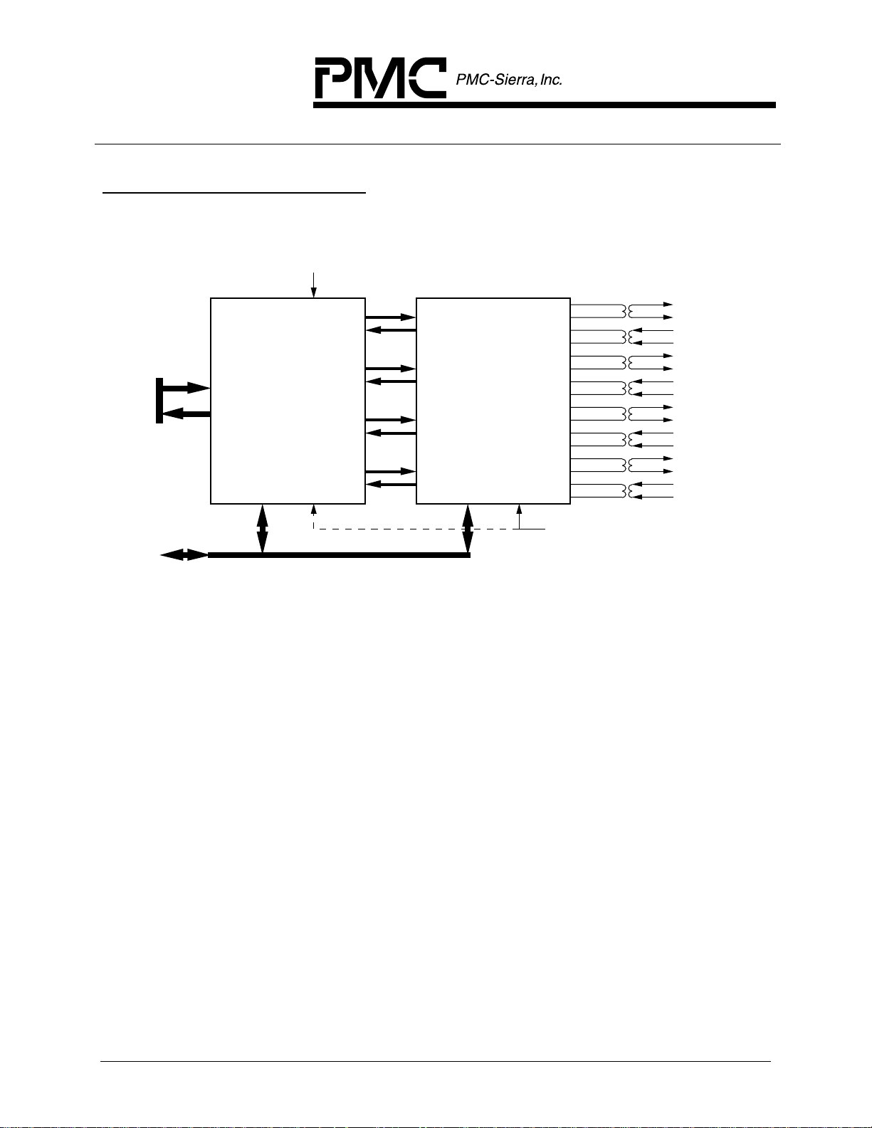
5 BLOCK DIAGRAM
Figure 4 - Normal Operating Mode
TCLKO[4:1]
TDP/TDD[4:1]
TDN/TOHO[4:1]
RCLKI[4:1]
RDP/RDD[4:1]
RDN/RLCV/
ROH[4:1]
XCLK
Digital
Transmit
Interface
Digital
Receive
Interface
Pulse
Density
Violation
Detector
RCLKO
Pulse
Density
Enforcer
HDLC
Receiver
RDLSIG/RDLINT[4:1]
RDLCLK/RDLEOM[4:1]
TDLCLK/TDLUDR[4:1]
TDLSIG/TDLINT[4:1]
HDLC
Transmitter
Bit
Oriented
Code
Receiver
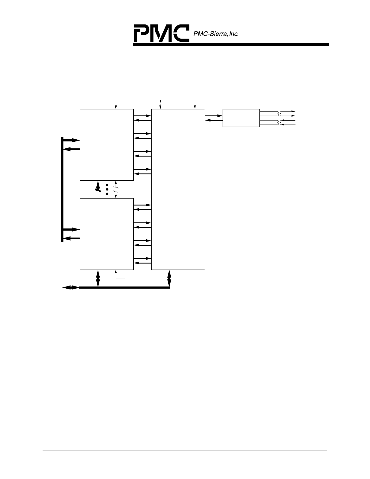
Figure 5 - Loopback Modes
Bit
Oriented
Code
Transmitter
T1/E1
Framing
Insertion
T1/E1
Framer
Performance
Monitor
TCLKI
Inband
Code
Detector
TFPI/TOHI
Inband
Loopback
Code
Generator
Alarms
Integrator
Tx ATM Cell
Processor
Rx ATM Cell
Processor
Microprocessor I/F
ALE
D[7:0]
A[10:0]
CSB
TDO
JTAG Test
Access Port
RDB
WRB
TDI
Tx ATM
4 Cell
FIFO
Rx ATM
4 Cell
FIFO
INTB
RSTB
TCK
TMS
TRSTB
TSOC
TDAT[7:0]
TXPRTY
TCA[4:1]
TCAMPH/TWRENB[4]
TWA[1]/TWRENB[3]
TWA[0]/TWRENB[2]
TWRMPHB /TWRENB[1]
MPHEN
TFCLK
RSOC
RDAT[7:0]
RXPRTY
RCA[4:1]
RCAMPH/RRDENB[4]
RRA[1]/RRDENB[3]
RRA[0]/RRDENB[2]
RRDMPHB /RRDENB[1]
RFCLK
Multi-
PHY
I/F
Bit
Oriented
Code
Transmitter
T1/E1
Framing
Insertion
T1/E1
Framer
Performance
Monitor
Inband
Code
Detector
Inband
Loopback
Code
Generator
PAYLOAD
LOOPBACK
Alarms
Integrator
JTAG Test
Access Port
Tx ATM Cell
Processor
Rx ATM Cell
Processor
Microprocessor I/F
Tx ATM
4 Cell
FIFO
Rx ATM
4 Cell
FIFO
Multi-
PHY
I/F
LINE
LOOPBACK
Digital
Transmit
Interface
Digital
Receive
Interface
Pulse
Density
Violation
Detector
Pulse
Density
Enforcer
DIAGNOSTIC
LOOPBACK
HDLC
Receiver
HDLC
Transmitter
Bit
Oriented
Code
Receiver
PROPRIETARY AND CONFIDENTIAL TO PMC-SIERRA, INC., AND FOR ITS CUSTOMERS’ INTERNAL USE 14
Page 31

PM7344 S/UNI-MPH
DATA SHEET
PMC-950449 ISSUE 6 MULTI-PHY USER NETWORK INTERFACE
6 DESCRIPTION
The PM7344 SATURN Quad T1/E1 Multi-PHY User Network Interface (S/UNIMPH) is a monolithic integrated circuit that implements the T1/E1 processing and
ATM mapping functions for four 1.544 Mbit/s or 2.048 Mbit/s ATM User Network
Interfaces. It can also be used in conjunction with external framing devices, to
implement ATM user network interfaces for other bit rates. For example, a quad
J2 (6.312 Mbit/s) interface can be realized with four external J2 framers and a
single S/UNI-MPH. It is fully compliant with both ANSI and ITU requirements and
ATM Forum UNI specifications. The S/UNI-MPH is software configurable,
allowing feature selection without changes to external wiring.
On the receive side, when configured for T1 processing, the S/UNI-MPH
recovers clock and data and can be configured to frame to either of the common
DS-1 signal formats; SF or ESF. Clock recovery may also be bypassed. The
S/UNI-MPH also supports detection of various alarm conditions such as loss of
signal, pulse density violation, red alarm, yellow alarm, and AIS alarm. The
S/UNI-MPH detects and indicates the presence of yellow and AIS patterns and
also integrates yellow, red, and AIS alarms as per industry specifications.
Performance monitoring with accumulation of CRC-6 errors, framing bit errors,
line code violations, and loss of frame events is provided. The S/UNI-MPH also
detects the presence of in-band loopback codes, ESF bit oriented codes, and
detects and terminates HDLC messages on the ESF data link.
On the receive side, when configured for E1 processing, the S/UNI-MPH
recovers clock and data and can be configured to frame to a basic G.704 2048
kbit/s signal or also frame to the signalling multiframe alignment signal and the
CRC multiframe alignment signal. Clock recovery may also be bypassed.
The S/UNI-MPH also supports detection of various alarm conditions such as loss
of signal, loss of frame, loss of signalling multiframe, loss of CRC multiframe,
and reception of remote alarm signal, remote multiframe alarm signal, alarm
indication signal, and timeslot 16 alarm indication signal. The S/UNI-MPH
detects and indicates the presence of remote alarm and AIS patterns and also
integrates red and AIS alarms as per industry specifications.
Performance monitoring with accumulation of CRC-4 errors, far end block errors,
framing bit errors, and line code violation is provided. The S/UNI-MPH also
detects and terminates HDLC messages on a data link. The data link may be
extracted from timeslot 16 or may be extracted from the national bits.
PROPRIETARY AND CONFIDENTIAL TO PMC-SIERRA, INC., AND FOR ITS CUSTOMERS’ INTERNAL USE 15
Page 32

PM7344 S/UNI-MPH
DATA SHEET
PMC-950449 ISSUE 6 MULTI-PHY USER NETWORK INTERFACE
For both T1 and E1 configurations, the S/UNI-MPH interprets the received frame
alignment and extracts the transmission format payload which carries the
received ATM cell payload.
The S/UNI-MPH frames to the ATM payload using cell delineation. HCS error
correction is optionally provided. Idle/unassigned cells may be dropped
according to a programmable filter. Cells are also dropped upon detection of an
uncorrectable header check sequence error. The ATM cell payloads are
descrambled.
Valid, assigned cells are written to a four cell FIFO buffer. These cells are read
from the FIFO using a synchronous 8 bit wide datapath interface with a cellbased handshake. Counts of received ATM cell headers that are errored and
uncorrectable, those that are errored and correctable and all passed cells are
accumulated independently for performance monitoring purposes. A multi-PHY
interface allows the four receive FIFOs (one for each T1 or E1 port) to be
serviced via a single 8 bit wide bus.
On the transmit side, when configured for T1 processing, the S/UNI-MPH
generates framing for SF and ESF DS1 formats. The S/UNI-MPH can also
generate in-band loopback codes, ESF bit oriented codes, and transmit HDLC
messages on the ESF data link.
On the transmit side, when configured for E1 processing, the S/UNI-MPH
generates framing for a basic G.704 2048 kbit/s signal. The signalling multiframe
alignment signal may be optionally inserted and the CRC multiframe structure
may be optionally inserted. HDLC messages on a data link can be transmitted.
The data link may be inserted into timeslot 16 or may be inserted into the
national bits.
For both T1 and E1 configurations, the S/UNI-MPH generates the transmitted
frame and inserts the transmit ATM cell payload into the transmission format
payload appropriately.
ATM cells are written to an internal programmable-length 4-cell FIFO using a
synchronous 8 bit wide datapath interface. Idle/unassigned cells are
automatically inserted when the internal FIFO contains less than one cell. The
S/UNI-MPH generates of the header check sequence and scrambles the payload
of the ATM cells. Each of these transmit ATM cell processing functions can be
enabled or bypassed. A multi-PHY interface allows the four transmit FIFOs
(one for each T1 or E1 port) to be serviced via a single 8 bit wide bus.
The S/UNI-MPH is configured, controlled and monitored via a generic 8-bit
microprocessor bus interface. The S/UNI-MPH also provides a standard 5 signal
P1149.1 JTAG test port for boundary scan board test purposes.
PROPRIETARY AND CONFIDENTIAL TO PMC-SIERRA, INC., AND FOR ITS CUSTOMERS’ INTERNAL USE 16
Page 33

PM7344 S/UNI-MPH
]
DATA SHEET
PMC-950449 ISSUE 6 MULTI-PHY USER NETWORK INTERFACE
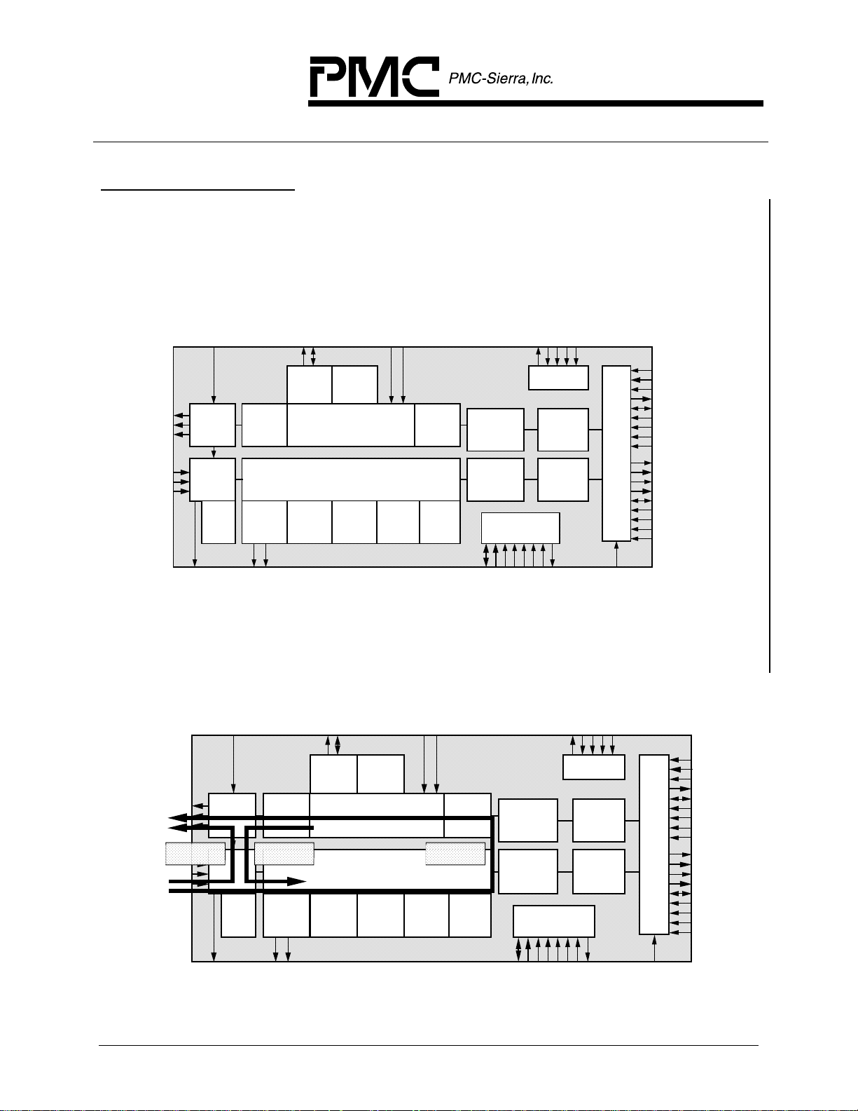
7 PIN DIAGRAM
VSS_DC[3]
ALE
PIN 128
RDB
WRB
A[10]
N/C
A[9]
A[8]
A[7]
A[6]
A[5]
A[4]
A[3]
VDD_DC[3
A[2]
A[1]
A[0]
CSB
RSTB
MPHEN
XCLK
TFPI/TOHI
TCLKI
TMS
TRSTB
TCK
PIN 103
PIN 1
RDP[1]/RDD[1]
RDN[1]/RLCV[1]/ROH[1]
RDN[2]/RLCV[2]/ROH[2]
RDN[3]/RLCV[3]/ROH[3]
TDLCLK[1]/TDLUDR[1]
TDLCLK[2]/TDLUDR[2]
TDLCLK[3]/TDLUDR[3]
TDLCLK[4]/TDLUDR[4]
RDN[4]/RLCV[4]/ROH[4]
RCLKI[1]
RDP[2]/RDD[2]
RCLKI[2]
RDP[3]/RDD[3]
RCLKI[3]
D[0]
D[1]
D[2]
D[3]
D[4]
D[5]
D[6]
D[7]
VDD_AC[0]
VSS_AC[0]
VDD_DC[0]
VSS_DC[0]
TCLKO[1]
TDP[1]/TDD[1]
TDN[1]/TOHO[1]
TCLKO[2]
TDP[2]/TDD[2]
TDN[2]/TOHO[2]
INTB
RDP[4]/RDD[4]
RCLKI[4]
TSOC
TXPRTY
TFCLK
PIN 38
Index Pin
PM7344
S/UNI-MPH
Top
View
PIN 102
TDI
TDO
RDLSIG[4]/RDLINT[4]
RDLSIG[3]/RDLINT[3]
RDLSIG[2]/RDLINT[2]
RDLSIG[1]/RDLINT[1]
RDAT[7]
RDAT[6]
RDAT[5]
RDAT[4]
RDAT[3]
RDAT[2]
RDAT[1]
RDAT[0]
VDD_AC[2]
VSS_AC[2]
VDD_DC[2]
VSS_DC[2]
RXPRTY
RSOC
RCAMPH/RRDENB[4]
RRA[1]/RRDENB[3]
RRA[0]/RRDENB[2]
RRDMPHB/RRDENB[1]
RDLCLK[4]/RDLEOM[4]
RDLCLK[3]/RDLEOM[3]
RDLCLK[2]/RDLEOM[2]
RDLCLK[1]/RDLEOM[1]
RFCLK
TDAT[7]
TDAT[6]
TDAT[5]
TDAT[4]
TDAT[3]
TDAT[2]
TDAT[1]
TDAT[0]
TWRMPHB/TWRENB[1]
PIN 65
TCA[1]
TCA[2]
TCA[3]
TCA[4]
RCA[1]
RCA[2]
RCA[3]
PIN 39 PIN 64
TDLSIG[1]/TDLINT[1]
TDLSIG[2]/TDLINT[2]
TDLSIG[3]/TDLINT[3]
PROPRIETARY AND CONFIDENTIAL TO PMC-SIERRA, INC., AND FOR ITS CUSTOMERS’ INTERNAL USE 17
TCLKO[3]
TDP[3]/TDD[3]
TDN[3]/TOHO[3]
TDLSIG[4]/TDLINT[4]
RCLKO
TCLKO[4]
VSS_AC[1]
VSS_DC[1]
VDD_AC[1]
VDD_DC[1]
TDP[4]/TDD[4]
TDN[4]/TOHO[4]
RCA[4]
TWA[1]/TWRENB[3]
TWA[0]/TWRENB[2]
TCAMPH/TWRENB[4]
Page 34

PM7344 S/UNI-MPH
DATA SHEET
PMC-950449 ISSUE 6 MULTI-PHY USER NETWORK INTERFACE
8 PIN DESCRIPTION
Pin Name Type Pin
No.
RDP[4]
Input Receive Digital Positive Line Pulse (RDP). This
RDP[3]
RDP[2]
RDP[1]/
RDD[4]
RDD[3]
RDD[2]
RDD[1]
33
7
4
1
Function
signal is available when the S/UNI-MPH is
configured to receive dual-rail formatted data.
The RDP input can be enabled for either RZ or
NRZ waveforms. When enabled for NRZ, RDP
may be enabled to be sampled on the rising or
falling edge of RCLKI. When enabled for RZ,
clock is recovered from the RDP and RDN
inputs.
Receive Digital Data (RDD). When the
S/UNI-MPH is configured to receive single-rail
data or when the T1/E1 framers are bypassed,
this signal contains the receive data stream.
RDD may be enabled to be sampled on the
rising or falling edge of RCLKI.
PROPRIETARY AND CONFIDENTIAL TO PMC-SIERRA, INC., AND FOR ITS CUSTOMERS’ INTERNAL USE 18
Page 35

PM7344 S/UNI-MPH
DATA SHEET
PMC-950449 ISSUE 6 MULTI-PHY USER NETWORK INTERFACE
Pin Name Type Pin
No.
RDN[4]
Input Receive Digital Negative Line Pulse (RDN).
RDN[3]
RDN[2]
RDN[1]/
RLCV[4]
RLCV[3]
RLCV[2]
RLCV[1]/
34
8
5
2
ROH[4]
ROH[3]
ROH[2]
ROH[1]
Function
This signal is available when the S/UNI-MPH is
configured to receive dual-rail formatted data.
The RDN input can be enabled for either RZ or
NRZ waveforms. When enabled for NRZ, RDN
may be enabled to be sampled on the rising or
falling edge of RCLKI. When enabled for RZ,
clock is recovered from the RDP and RDN
inputs.
Receive Line Code Violation Indication (RLCV).
When the S/UNI-MPH is configured to receive
single-rail data, this signal contains line code
violation indications that are detected by the
upstream line interface unit (LIU). RLCV may
be enabled to be sampled on the rising or falling
edge of RCLKI.
Receive Overhead Mask (ROH). When the
S/UNI-MPH is configured to bypass the T1/E1
framers, this signal indicates the framing
overhead in the receive stream, thus allowing
the S/UNI-MPH to provide a user network
interface for arbitrary bit rates (such as the
6.312 Mbit/s J2 rate). ROH may be configured
to be active high or active low, and may be
enabled to be sampled on the rising or falling
edge of RCLKI.
RCLKI[4]
RCLKI[3]
RCLKI[2]
RCLKI[1]
Input 35
9
6
3
Receive Line Clock Input (RCLKI). This signal is
the externally recovered line clock that may be
enabled to sample the RDP and RDN inputs on
its rising or falling edge when the input format is
enabled for dual-rail NRZ; or to sample the RDD
and RLCV/ROH inputs on its rising or falling
edge when the input format is enabled for
single-rail, or when the T1/E1 framers are
bypassed. RCLKI must operate at frequencies
less than or equal to 25 MHz.
PROPRIETARY AND CONFIDENTIAL TO PMC-SIERRA, INC., AND FOR ITS CUSTOMERS’ INTERNAL USE 19
Page 36

PM7344 S/UNI-MPH
DATA SHEET
PMC-950449 ISSUE 6 MULTI-PHY USER NETWORK INTERFACE
Pin Name Type Pin
Function
No.
RCLKO Output 49 Receive Clock Output (RCLKO). This signal is
recovered from the RDP and RDN inputs (if the
input format is dual-rail RZ), or from the RCLKI
input (if the input format is NRZ or if the T1/E1
framers are bypassed). Any one of the four sets
of RDP/RDN or RCLKI signals may be selected
as the source of RCLKO using internal registers.
RDLSIG[4]
RDLSIG[3]
RDLSIG[2]
RDLSIG[1]/
Output 100
99
98
97
Receive Data Link Signal (RDLSIG). The
RDLSIG signal is available on this pin when the
internal HDLC receiver (RFDL) is disabled from
use. When the S/UNI-MPH is configured to
receive T1-ESF formatted data, RDLSIG
contains the data stream extracted from the
facility data link; when the S/UNI-MPH is
configured to receive T1-SF formatted data, the
RDLSIG output is held low; when the S/UNIMPH is configured to receive E1 formatted data,
RDLSIG contains the data stream extracted
from timeslot 16 or a data stream made up of
any combination of the national bits. RDLSIG is
updated on the falling edge of RDLCLK.
RDLINT[4]
RDLINT[3]
RDLINT[2]
RDLINT[1]
Receive Data Link Interrupt (RDLINT). The
RDLINT signal is available on this pin when
RFDL is enabled. RDLINT goes high when an
event occurs which changes the status of the
HDLC receiver.
PROPRIETARY AND CONFIDENTIAL TO PMC-SIERRA, INC., AND FOR ITS CUSTOMERS’ INTERNAL USE 20
Page 37

PM7344 S/UNI-MPH
DATA SHEET
PMC-950449 ISSUE 6 MULTI-PHY USER NETWORK INTERFACE
Pin Name Type Pin
No.
RDLCLK[4]
RDLCLK[3]
RDLCLK[2]
RDLCLK[1]/
Output 78
77
76
75
RDLEOM[4]
RDLEOM[3]
RDLEOM[2]
RDLEOM[1]
TDLSIG[4]
TDLSIG[3]
TDLSIG[2]
TDLSIG[1]/
I/O 42
41
40
39
Function
Receive Data Link Clock (RDLCLK). The
RDLCLK signal is available on this pin when the
internal HDLC receiver (RFDL) is disabled from
use. RDLCLK is used to process the data
stream contained on RDLSIG. When the S/UNIMPH is configured to receive T1-SF formatted
data, or when the T1/E1 framers are bypassed,
RDLCLK is held low. In all other formats the
rising edge of RDLCLK can be used to sample
the data on RDLSIG.
Receive Data Link End of Message (RDLEOM).
The RDLEOM signal is available on this pin
when RFDL is enabled. RDLEOM goes high
when the last byte of a received sequence is
read from the RFDL FIFO buffer, or when the
FIFO buffer is overrun.
Transmit Data Link Signal (TDLSIG). The
TDLSIG signal is input on this pin when the
internal HDLC transmitter (XFDL) is disabled
from use. TDLSIG is the source for the data
stream to be inserted into the data link. When
the S/UNI-MPH is configured to transmit T1-ESF
formatted data, TDLSIG contains the data
stream inserted in the facility data link; when the
S/UNI-MPH is configured to transmit T1-SF
formatted data, TDLSIG is ignored; when the
S/UNI-MPH is configured to transmit E1
formatted data, TDLSIG contains the data
stream inserted in timeslot 16 or a data stream
inserted in any combination of the national bits.
TDLSIG is sampled on the rising edge of
TDLCLK.
TDLINT[4]
TDLINT[3]
TDLINT[2]
TDLINT[1]
Transmit Data Link Interrupt (TDLINT). The
TDLINT signal is output on this pin when XFDL
is enabled. TDLINT goes high when the last
data byte written to the XFDL has been set up
for transmission and processor intervention is
required to either write control information to end
the message, or to provide more data.
PROPRIETARY AND CONFIDENTIAL TO PMC-SIERRA, INC., AND FOR ITS CUSTOMERS’ INTERNAL USE 21
Page 38

PM7344 S/UNI-MPH
DATA SHEET
PMC-950449 ISSUE 6 MULTI-PHY USER NETWORK INTERFACE
Pin Name Type Pin
No.
TDLCLK[4]
TDLCLK[3]
TDLCLK[2]
TDLCLK[1]/
Output 31
30
29
28
TDLUDR[4]
TDLUDR[3]
TDLUDR[2]
TDLUDR[1]
TCLKO[4]
TCLKO[3]
TCLKO[2]
TCLKO[1]
Output 48
45
25
22
Function
Transmit Data Link Clock (TDLCLK). The
TDLCLK signal is available on this pin when the
internal HDLC transmitter (XFDL) is disabled
from use. The rising edge of TDLCLK is used to
sample the data stream contained on the
TDLSIG input. When the S/UNI-MPH is
configured to transmit T1-SF formatted data, or
when the T1/E1 framers are bypassed, TDLCLK
is held low.
Transmit Data Link Underrun (TDLUDR). The
TDLUDR signal is available on this pin when
XFDL is enabled. TDLUDR goes high when the
processor has failed to service the TDLINT
interrupt before the transmit buffer is emptied.
Transmit Clock Output (TCLKO). The TDP,
TDN, and TDD outputs may be enabled to be
updated on the rising or falling edge of TCLKO.
TCLKO is the transmit clock that is adequately
jitter and wander free in absolute terms to permit
an acceptable transmission signal to be
generated. Depending on the configuration of
the S/UNI-MPH, TCLKO may be derived from
TCLKI, RCLKO, or XCLK, with or without jitter
attenuation.
TDP[4]
TDP[3]
TDP[2]
TDP[1]/
Output 46
43
26
23
Transmit Digital Positive Line Pulse (TDP). This
signal is available on the pin when the S/UNIMPH is configured to transmit dual-rail data.
The TDP signal can be formatted for either RZ
or NRZ waveforms, and can be enabled to be
updated on the rising or falling edge of TCLKO.
TDD[4]
TDD[3]
TDD[2]
TDD[1]
Transmit Digital Data (TDD). This signal is
available on the pin when the S/UNI-MPH is
configured to transmit single-rail data, or when
the T1/E1 framers are bypassed. The TDD
signal may be enabled to be updated on the
rising or falling edge of TCLKO.
PROPRIETARY AND CONFIDENTIAL TO PMC-SIERRA, INC., AND FOR ITS CUSTOMERS’ INTERNAL USE 22
Page 39

PM7344 S/UNI-MPH
DATA SHEET
PMC-950449 ISSUE 6 MULTI-PHY USER NETWORK INTERFACE
Pin Name Type Pin
No.
TDN[4]
TDN[3]
TDN[2]
TDN[1]/
Output 47
44
27
24
TOHO[4]
TOHO[3]
TOHO[2]
TOHO[1]
Function
Transmit Digital Negative Line Pulse (TDN).
This signal is available on the pin when the
S/UNI-MPH is configured to transmit dual-rail
data. The TDN signal can be formatted for
either RZ or NRZ waveforms, and can be
enabled to be updated on the rising or falling
edge of TCLKO. When configured for single-rail
T1 or E1 data, TDN is unused.
Transmit Overhead Mask Output (TOHO).
When the S/UNI-MPH is configured to bypass
the T1/E1 transmit framers, this signal indicates
the placeholder bit positions for the framing
overhead in the transmit stream. TOHO may be
connected to an external framer device to
provide a user network interface for arbitrary bit
rates or for the J2 rate (for which TOHO is
specially conditioned to operate with the
Transwitch JT2F framer). The ATM cell stream
can be configured to be byte aligned to TOHO
(in which case the number of TCLKO periods
between active TOHO edges must be divisible
by eight). TOHO may be configured to be active
high or active low, and may be enabled to be
updated on the rising or falling edge of TCLKO.
TCLKI Input 107 Transmit Clock Input (TCLKI). This signal
provides the transmit direction timing (when the
S/UNI-MPH is not loop timed). The S/UNI-MPH
may be configured to ignore the TCLKI input
and utilize XCLK instead. The default
requirement is for TCLKI to be a 1.544 MHz
clock for T1 or a 2.048 MHz clock for E1. For
arbitrary bit rates, TCLKI must be less than or
equal to 25 MHz.
PROPRIETARY AND CONFIDENTIAL TO PMC-SIERRA, INC., AND FOR ITS CUSTOMERS’ INTERNAL USE 23
Page 40

PM7344 S/UNI-MPH
DATA SHEET
PMC-950449 ISSUE 6 MULTI-PHY USER NETWORK INTERFACE
Pin Name Type Pin
Function
No.
TFPI Input 106 Transmit Frame Position (TFPI). This signal
provides the transmit frame position indication
for the four T1/E1 framers. TFPI can be used in
applications where the transmit frames must be
aligned to a common reference. In these
applications, TFPI is activated for one clock
period every 193 (T1) or 256 (E1) TCLKI periods
(or multiple thereof). If such alignment is not
required, TFPI may be tied low. TFPI may be
configured to be active high or active low, and
may be enabled to be sampled on the rising or
falling edge of TCLKI.
TOHI Transmit Overhead Mask Input (TOHI). This
signal identifies the placeholder bits in the
transmit stream for arbitrary bit rate interfaces.
A delayed version of TOHI appears on the four
TOHO outputs. Downstream framing insertion
devices overwrite the placeholder bit positions
with overhead specific to a particular frame
format (for example the 6.312 Mbit/s J2 format).
TOHI may be configured to be active high or
active low, and may be enabled to be sampled
on the rising or falling edge of TCLKI.
XCLK/ Input 108 Crystal Clock Input (XCLK). This signal
provides timing for the T1 or E1 framer portion
of the S/UNI-MPH. Depending on the
configuration of the S/UNI-MPH, XCLK must be
nominally 24x or 8x the nominal line rate. The
8x clock is used by the clock recovery digital
phase locked loop and the T1/E1 framer, while
the 24x clock is used by the jitter attenuator in
the S/UNI-MPH. This clock may be tied low if
the T1/E1 framers are bypassed. The default
requirement is for XCLK to be a 37.056 MHz
clock for T1 or a 49.152 MHz clock for E1.
VCLK Vector Clock (VCLK). The VCLK signal is used
during S/UNI-MPH production test to verify
internal functionality.
PROPRIETARY AND CONFIDENTIAL TO PMC-SIERRA, INC., AND FOR ITS CUSTOMERS’ INTERNAL USE 24
Page 41

PM7344 S/UNI-MPH
DATA SHEET
PMC-950449 ISSUE 6 MULTI-PHY USER NETWORK INTERFACE
Pin Name Type Pin
Function
No.
MPHEN Input 109 Multiphy Enable (MPHEN). This input selects
the configuration of the receive and transmit cell
interfaces. When MPHEN is high, the cell
interfaces are configured for multi-phy
addressing and signals TWRMPHB, TWA[1:0],
TCAMPH, RRDMPHB, RRA[1:0], and RCAMPH
are active. When MPHEN is low, the cell
interfaces are configured for direct phy selection
and signals TWRENB[4:1] and RRDENB[4:1]
are active.
RFCLK Input 74 Receive FIFO Read Clock (RFCLK). This signal
is used to read ATM cells from the receive
FIFOs. RFCLK must cycle at a 25 MHz or lower
instantaneous rate, but at a high enough rate to
avoid FIFO overflow.
PROPRIETARY AND CONFIDENTIAL TO PMC-SIERRA, INC., AND FOR ITS CUSTOMERS’ INTERNAL USE 25
Page 42

PM7344 S/UNI-MPH
DATA SHEET
PMC-950449 ISSUE 6 MULTI-PHY USER NETWORK INTERFACE
Pin Name Type Pin
Function
No.
RRDMPHB Input 79 Receive Multi-Phy Read Enable (RRDMPHB).
The RRDMPHB signal is available on this pin
when input MPHEN is high. RRDMPHB is used
to initiate reads from the receive FIFOs. When
sampled low using the rising edge of RFCLK, a
byte is read from the receive FIFO selected by
the RRA[1:0] address bus (if one is available)
and output on bus RDAT[7:0]. When sampled
high using the rising edge of RFCLK, no read is
performed and RDAT[7:0] and RSOC are
tristated. RRDMPHB must operate in
conjunction with RFCLK to access the FIFOs at
a high enough instantaneous rate as to avoid
FIFO overflows. The ATM layer device may
deassert RRDMPHB at anytime it is unable to
accept another byte.
RRDENB[1] Receive Read Enable PHY #1 (RRDENB[1]).
The RRDENB[1] signal is available on this pin
when input MPHEN is low. RRDENB[1] is used
to initiate reads from the receive FIFO of PHY
#1. When sampled low using the rising edge of
RFCLK (and the remaining three RRDENBs
remain high), a byte is read from PHY #1's
synchronous FIFO and output on bus RDAT[7:0]
if one is available. When sampled high using
the rising edge of RFCLK, no read is performed
and RDAT[7:0] and RSOC are tristated.
RRDENB[1] must operate in conjunction with
RFCLK to access the FIFOs at a high enough
instantaneous rate as to avoid FIFO overflows.
The ATM layer device may deassert RRDENB[1]
at anytime it is unable to accept another byte.
PROPRIETARY AND CONFIDENTIAL TO PMC-SIERRA, INC., AND FOR ITS CUSTOMERS’ INTERNAL USE 26
Page 43

PM7344 S/UNI-MPH
DATA SHEET
PMC-950449 ISSUE 6 MULTI-PHY USER NETWORK INTERFACE
Pin Name Type Pin
Function
No.
RRA[0] Input 80 Receive Read Address LSB (RRA[0]). The
RRA[0] signal is available on this pin when input
MPHEN is high. RRA[0] is used (along with
RRA[1]) to select the FIFO (and hence port) that
is read from using the RRDMPHB signal.
RRA[0] is sampled on the rising edge of RFCLK
together with RRDMPHB.
RRDENB[2] Receive Read Enable PHY #2 (RRDENB[2]).
The RRDENB[2] signal is available on this pin
when input MPHEN is low. RRDENB[2] is used
to initiate reads from the receive FIFO of PHY
#2. When sampled low using the rising edge of
RFCLK (and the remaining three RRDENBs
remain high), a byte is read from PHY #2's
synchronous FIFO and output on bus RDAT[7:0]
if one is available. When sampled high using
the rising edge of RFCLK, no read is performed
and RDAT[7:0] and RSOC are tristated.
RRDENB[2] must operate in conjunction with
RFCLK to access the FIFOs at a high enough
instantaneous rate as to avoid FIFO overflows.
The ATM layer device may deassert RRDENB[2]
at anytime it is unable to accept another byte.
PROPRIETARY AND CONFIDENTIAL TO PMC-SIERRA, INC., AND FOR ITS CUSTOMERS’ INTERNAL USE 27
Page 44

PM7344 S/UNI-MPH
DATA SHEET
PMC-950449 ISSUE 6 MULTI-PHY USER NETWORK INTERFACE
Pin Name Type Pin
Function
No.
RRA[1] Input 81 Receive Read Address MSB (RRA[1]). The
RRA[1] signal is available on this pin when input
MPHEN is high. RRA[1] is used (along with
RRA[0]) to select the FIFO (and hence port) that
is read from using the RRDMPHB signal.
RRA[1] is sampled on the rising edge of RFCLK
together with RRDMPHB.
RRDENB[3] Receive Read Enable PHY #3 (RRDENB[3]).
The RRDENB[3] signal is available on this pin
when input MPHEN is low. RRDENB[3] is used
to initiate reads from the receive FIFO of PHY
#3. When sampled low using the rising edge of
RFCLK (and the remaining three RRDENBs
remain high), a byte is read from PHY #3's
synchronous FIFO and output on bus RDAT[7:0]
if one is available. When sampled high using
the rising edge of RFCLK, no read is performed
and RDAT[7:0] and RSOC are tristated.
RRDENB[3] must operate in conjunction with
RFCLK to access the FIFOs at a high enough
instantaneous rate as to avoid FIFO overflows.
The ATM layer device may deassert RRDENB[3]
at anytime it is unable to accept another byte.
PROPRIETARY AND CONFIDENTIAL TO PMC-SIERRA, INC., AND FOR ITS CUSTOMERS’ INTERNAL USE 28
Page 45

PM7344 S/UNI-MPH
DATA SHEET
PMC-950449 ISSUE 6 MULTI-PHY USER NETWORK INTERFACE
Pin Name Type Pin
Function
No.
RCAMPH I/O 82 Receive Multi-Phy Cell Available (RCAMPH).
The RCAMPH signal is output on this pin when
input MPHEN is high. This signal indicates
when a cell is available in the receive FIFO for
the port selected by RRA[1:0]. RCAMPH can be
configured to be deasserted when either zero or
four bytes remain in the selected/addressed
FIFO. RCAMPH will thus transition low on the
rising edge of RFCLK after the 53rd or 48th byte
has been output if the PHY being polled is the
same as the PHY in use .
RRDENB[4] Receive Read Enable PHY #4 (RRDENB[4]).
The RRDENB[4] signal is input on this pin when
input MPHEN is low. RRDENB[4] is used to
initiate reads from the receive FIFO of PHY #4.
When sampled low using the rising edge of
RFCLK (and the remaining three RRDENBs
remain high), a byte is read from PHY #4's
synchronous FIFO and output on bus RDAT[7:0]
if one is available. When sampled high using
the rising edge of RFCLK, no read is performed
and RDAT[7:0] and RSOC are tristated.
RRDENB[4] must operate in conjunction with
RFCLK to access the FIFOs at a high enough
instantaneous rate as to avoid FIFO overflows.
The ATM layer device may deassert RRDENB[4]
at anytime it is unable to accept another byte.
RDAT[0]
RDAT[1]
RDAT[2]
RDAT[3]
RDAT[4]
RDAT[5]
RDAT[6]
RDAT[7]
PROPRIETARY AND CONFIDENTIAL TO PMC-SIERRA, INC., AND FOR ITS CUSTOMERS’ INTERNAL USE 29
Tristate
Output
89
90
91
92
93
94
95
96
Receive Cell Data Bus (RDAT[7:0]). This bus
carries the ATM cell octets that are read from
the selected receive FIFO. RDAT[7:0] is
updated on the rising edge of RFCLK and is
tristated when RRDENB[n]/RRDMPHB is high.
Page 46

PM7344 S/UNI-MPH
DATA SHEET
PMC-950449 ISSUE 6 MULTI-PHY USER NETWORK INTERFACE
Pin Name Type Pin
No.
RXPRTY Tristate
84 Receive Parity (RXPRTY). This signal indicates
Output
RSOC Tristate
83 Receive Start of Cell (RSOC). This signal marks
Output
RCA[4]
RCA[3]
RCA[2]
RCA[1]
Output 61
60
59
58
Function
the parity of the RDAT[7:0] bus. Odd or even
parity selection can be made using a register.
RXPRTY is updated on the rising edge of
RFCLK and is tristated when
RRDENB[4:1]/RRDMPHB is high.
the start of cell on the RDAT[7:0] bus. When
RSOC is high, the first octet of the cell is present
on the RDAT[7:0] stream. RSOC is updated on
the rising edge of RFCLK and is tristated when
RRDENB[4:1]/RRDMPHB is high.
Receive Cell Available (RCA[4:1]). These output
signals indicate when a cell is available in the
receive FIFO for the corresponding port.
RCA[4:1] can be configured to be deasserted
when either zero or four bytes remain in the
FIFO. RCA[4:1] will thus transition low on the
rising edge of RFCLK after the 53rd or 48th byte
has been output.
TFCLK Input 38 Transmit FIFO Write Clock (TFCLK). This signal
is used to write ATM cells to the four cell
transmit FIFOs. TFCLK cycles at a 25 MHz or
lower instantaneous rate. A complete 53 octet
cell must be written to the FIFO before being
inserted in the transmit stream. Idle/unassigned
cells are inserted when a complete cell is not
available.
TDAT[0]
TDAT[1]
TDAT[2]
TDAT[3]
TDAT[4]
TDAT[5]
TDAT[6]
TDAT[7]
Input 66
67
68
69
70
71
72
73
Transmit Cell Data Bus (TDAT[7:0]). This bus
carries the ATM cell octets that are written to the
selected transmit FIFO. TDAT[7:0] is sampled
on the rising edge of TFCLK and is considered
valid only when TWRENB[n]/TWRMPHB is
simultaneously asserted.
PROPRIETARY AND CONFIDENTIAL TO PMC-SIERRA, INC., AND FOR ITS CUSTOMERS’ INTERNAL USE 30
Page 47

PM7344 S/UNI-MPH
DATA SHEET
PMC-950449 ISSUE 6 MULTI-PHY USER NETWORK INTERFACE
Pin Name Type Pin
Function
No.
TXPRTY Input 37 Transmit bus parity (TXPRTY). This signal
indicates the parity of the TDAT[7:0] bus. Odd or
even parity selection can be made using a
register. TXPRTY is sampled on the rising edge
of TFCLK and is considered valid only when
TWRENB[n]/TWRMPHB is simultaneously
asserted.
A parity error is indicated by a status bit and a
maskable interrupt. Cells with parity errors are
inserted in the transmit stream, so the TXPRTY
input may be unused.
TWRMPHB Input 65 Transmit Multi-Phy Write Enable (TWRMPHB).
The TWRMPHB signal is available on this pin
when input MPHEN is high. This active low
input is used to initiate writes to the transmit
FIFOs. When sampled low using the rising
edge of TFCLK, the byte on TDAT[7:0] is written
into the transmit FIFO selected by the TWA[1:0]
address bus. When sampled high using the
rising edge of TFCLK, no write is performed. A
complete 53 octet cell must be written to the
transmit FIFO before it is inserted into the
transmit stream. Idle/unassigned cells are
inserted when a complete cell is not available.
TWRENB[1
]
Transmit Write Enable PHY #1 (TWRENB[1]).
The TWRENB[1] signal is available on this pin
when input MPHEN is low. TWRENB[1] is used
to initiate writes to the transmit FIFO of PHY #1.
When sampled low using the rising edge of
TFCLK (and the remaining three TWRENBs
remain high), a byte is written to PHY #1's
synchronous FIFO. When sampled high using
the rising edge of TFCLK, no write is performed.
TWRENB[1] must operate in conjunction with
TFCLK to access the FIFOs at a high enough
instantaneous rate as to avoid FIFO overflows.
The ATM layer device may deassert
TWRENB[1] at anytime it is unable to provide
another byte.
PROPRIETARY AND CONFIDENTIAL TO PMC-SIERRA, INC., AND FOR ITS CUSTOMERS’ INTERNAL USE 31
Page 48

PM7344 S/UNI-MPH
DATA SHEET
PMC-950449 ISSUE 6 MULTI-PHY USER NETWORK INTERFACE
Pin Name Type Pin
Function
No.
TWA[0] Input 64 Transmit Write Address LSB (TWA[0]). The
TWA[0] signal is available on this pin when input
MPHEN is high. TWA[0] is used (along with
TWA[1]) to select the FIFO (and hence port) that
is written to using the TWRMPHB signal.
TWA[0] is sampled on the rising edge of TFCLK
together with TWRMPHB.
TWRENB[2
]
Transmit Write Enable PHY #2 (TWRENB[2]).
The TWRENB[2] signal is available on this pin
when input MPHEN is low. TWRENB[2] is used
to initiate writes to the transmit FIFO of PHY #2.
When sampled low using the rising edge of
TFCLK (and the remaining three TWRENBs
remain high), a byte is written to PHY #2's
synchronous FIFO. When sampled high using
the rising edge of TFCLK, no write is performed.
TWRENB[2] must operate in conjunction with
TFCLK to access the FIFOs at a high enough
instantaneous rate as to avoid FIFO overflows.
The ATM layer device may deassert
TWRENB[2] at anytime it is unable to provide
another byte.
PROPRIETARY AND CONFIDENTIAL TO PMC-SIERRA, INC., AND FOR ITS CUSTOMERS’ INTERNAL USE 32
Page 49

PM7344 S/UNI-MPH
DATA SHEET
PMC-950449 ISSUE 6 MULTI-PHY USER NETWORK INTERFACE
Pin Name Type Pin
Function
No.
TWA[1] Input 63 Transmit Write Address MSB (TWA[1]). The
TWA[1] signal is available on this pin when input
MPHEN is high. TWA[1] is used (along with
TWA[0]) to select the FIFO (and hence port) that
is written to using the TWRMPHB signal.
TWA[1] is sampled on the rising edge of TFCLK
together with TWRMPHB.
TWRENB[3
]
Transmit Write Enable PHY #3 (TWRENB[3]).
The TWRENB[3] signal is available on this pin
when input MPHEN is low. TWRENB[3] is used
to initiate writes to the transmit FIFO of PHY #3.
When sampled low using the rising edge of
TFCLK (and the remaining three TWRENBs
remain high), a byte is written to PHY #3's
synchronous FIFO. When sampled high using
the rising edge of TFCLK, no write is performed.
TWRENB[3] must operate in conjunction with
TFCLK to access the FIFOs at a high enough
instantaneous rate as to avoid FIFO overflows.
The ATM layer device may deassert
TWRENB[3] at anytime it is unable to provide
another byte.
PROPRIETARY AND CONFIDENTIAL TO PMC-SIERRA, INC., AND FOR ITS CUSTOMERS’ INTERNAL USE 33
Page 50

PM7344 S/UNI-MPH
DATA SHEET
PMC-950449 ISSUE 6 MULTI-PHY USER NETWORK INTERFACE
Pin Name Type Pin
Function
No.
TCAMPH I/O 62 Transmit Multi-Phy Cell Available (TCAMPH).
The TCAMPH signal is output on this pin when
input MPHEN is high. This signal indicates
when a cell is available in the transmit FIFO for
the port selected by TWA[1:0]. When high,
TCAMPH indicates that the corresponding
transmit FIFO is not full and a complete cell may
be written. When TCAMPH goes low, it can be
configured to indicate either that the
corresponding transmit FIFO is near full and can
accept no more than four writes or that the
corresponding transmit FIFO is full. TCAMPH
will thus transition low on the rising edge of
TFCLK on which the 52nd or 48th byte is
sampled if the PHY being polled is the same as
the PHY in use. To reduce FIFO latency, the
FIFO depth at which TCAMPH indicates "full"
can be set to one, two, three or four cells.
TWRENB[4
]
Transmit Write Enable PHY #4 (TWRENB[4]).
The TWRENB[4] signal is input on this pin when
input MPHEN is low. TWRENB[4] is used to
initiate writes to the transmit FIFO of PHY #4.
When sampled low using the rising edge of
TFCLK (and the remaining three TWRENBs
remain high), a byte is written to PHY #4's
synchronous FIFO. When sampled high using
the rising edge of TFCLK, no write is performed.
TWRENB[4] must operate in conjunction with
TFCLK to access the FIFOs at a high enough
instantaneous rate as to avoid FIFO overflows.
The ATM layer device may deassert
TWRENB[4] at anytime it is unable to provide
another byte.
PROPRIETARY AND CONFIDENTIAL TO PMC-SIERRA, INC., AND FOR ITS CUSTOMERS’ INTERNAL USE 34
Page 51

PM7344 S/UNI-MPH
DATA SHEET
PMC-950449 ISSUE 6 MULTI-PHY USER NETWORK INTERFACE
Pin Name Type Pin
Function
No.
TSOC Input 36 Transmit Start of Cell (TSOC). This input marks
the start of cell on the TDAT[7:0] bus. When
TSOC is high, the first octet of the cell is present
on the TDAT[7:0] stream. It is not necessary for
TSOC to be present at each cell. An interrupt
may be generated if TSOC is high during any
byte other than the first byte. TSOC is sampled
on the rising edge of TFCLK
TCA[4]
TCA[3]
TCA[2]
TCA[1]
Output 57
56
55
54
Transmit Cell Available (TCA[4:1]). These
output signals indicate when a cell is available in
the transmit FIFO for the corresponding port.
When high, TCA indicates that the
corresponding transmit FIFO is not full and a
complete cell may be written. When TCA goes
low, it can be configured to indicate either that
the corresponding transmit FIFO is near full and
can accept no more than four writes or that the
corresponding transmit FIFO is full. TCA[4:1]
will thus transition low on the rising edge of
TFLCK on which the 52nd or 48th byte is
sampled. To reduce FIFO latency, the FIFO
depth at which TCA indicates "full" can be set to
one, two, three or four cells.
INTB Output 32 Active low Open-Drain Interrupt (INTB). This
signal goes low when an unmasked interrupt
event is detected on any of the internal interrupt
sources, including the internal HDLC
transceivers. Note that INTB will remain low
until all active, unmasked interrupt sources are
acknowledged at their source.
CSB Input 113 Active low Chip Select (CSB). This signal must
be low to enable S/UNI-MPH register accesses.
If CSB is not used, (RDB and WRB determine
register reads and writes) then it should be tied
to an inverted version of RSTB.
PROPRIETARY AND CONFIDENTIAL TO PMC-SIERRA, INC., AND FOR ITS CUSTOMERS’ INTERNAL USE 35
Page 52

PM7344 S/UNI-MPH
DATA SHEET
PMC-950449 ISSUE 6 MULTI-PHY USER NETWORK INTERFACE
Pin Name Type Pin
Function
No.
D[7]
D[6]
D[5]
D[4]
D[3]
D[2]
D[1]
D[0]
I/O 17
16
15
14
13
12
11
10
Bidirectional Data Bus (D[7:0]). This bus is used
during S/UNI-MPH read and write accesses.
RDB Input 112 Active low Read Enable (RDB). This signal is
pulsed low to enable a S/UNI-MPH register read
access. The S/UNI-MPH drives the D[7:0] bus
with the contents of the addressed register while
RDB and CSB are both low.
WRB Input 111 Active low Write Strobe (WRB). This signal is
pulsed low to enable a S/UNI-MPH register write
access. The D[7:0] bus is clocked into the
addressed register on the rising edge of WRB
while CSB is low.
ALE Input 114 Address Latch Enable (ALE). This signal latches
the address bus contents, A[10:0], when low,
allowing the S/UNI-MPH to be interfaced to a
multiplexed address/data bus. When ALE is
high, the address latches are transparent. ALE
has an integral pull-up resistor.
RSTB Input 110 Active low Reset (RSTB). This signal is set low
to asynchronously reset the S/UNI-MPH. RSTB
is a Schmitt-trigger input with an integral pull-up
resistor.
A[0]
A[1]
A[2]
A[3]
A[4]
A[5]
A[6]
A[7]
A[8]
A[9]
A[10]
Input 117
118
119
120
121
122
123
124
125
126
127
Address Bus (A[10:0]). This bus selects specific
registers during S/UNI-MPH register accesses.
PROPRIETARY AND CONFIDENTIAL TO PMC-SIERRA, INC., AND FOR ITS CUSTOMERS’ INTERNAL USE 36
Page 53

PM7344 S/UNI-MPH
DATA SHEET
PMC-950449 ISSUE 6 MULTI-PHY USER NETWORK INTERFACE
Pin Name Type Pin
Function
No.
TCK Input 103 Test Clock (TCK). This signal provides timing for
test operations that can be carried out using the
IEEE P1149.1 test access port.
TMS Input 104 Test Mode Select (TMS). This signal controls the
test operations that can be carried out using the
IEEE P1149.1 test access port. TMS is sampled
on the rising edge of TCK. TMS has an integral
pull up resistor.
TDI Input 102 Test Data Input (TDI). This signal carries test
data into the S/UNI-MPH via the IEEE P1149.1
test access port. TDI is sampled on the rising
edge of TCK. TDI has an integral pull up
resistor.
TDO Tristate
Output
101 Test Data Output (TDO). This signal carries test
data out of the S/UNI-MPH via the IEEE
P1149.1 test access port. TDO is updated on
the falling edge of TCK. TDO is a tri-state
output which is inactive except when scanning
of data is in progress.
TRSTB Input 105 Active low Test Reset (TRSTB). This signal
provides an asynchronous S/UNI-MPH test
access port reset via the IEEE P1149.1 test
access port. TRSTB is a Schmitt triggered input
with an integral pull up resistor. TRSTB must be
asserted during the power up sequence.
Note that if not used, TRSTB must be
connected to the RSTB input.
VDD_AC[2]
VDD_AC[1]
VDD_AC[0]
VDD_DC[3]
VDD_DC[2]
VDD_DC[1]
VDD_DC[0]
VSS_AC[2]
VSS_AC[1]
VSS_AC[0]
Power 88
50
18
Power 116
86
52
20
Ground 87
51
19
Pad Ring Power (VDD_AC[2:0]). These pins
should be connected to a well decoupled +5 V
DC in common with VDD_DC[3:0]
DC Power (VDD_DC[3:0]). These pins should
be connected to a well decoupled +5 V DC in
common with VDD_AC[2:0].
Pad Ring Ground (VSS_AC[2:0]). These pins
should be connected to GND in common with
VSS_DC[3:0].
PROPRIETARY AND CONFIDENTIAL TO PMC-SIERRA, INC., AND FOR ITS CUSTOMERS’ INTERNAL USE 37
Page 54

PM7344 S/UNI-MPH
DATA SHEET
PMC-950449 ISSUE 6 MULTI-PHY USER NETWORK INTERFACE
Pin Name Type Pin
Function
No.
VSS_DC[3]
VSS_DC[2]
VSS_DC[1]
VSS_DC[0]
Ground 115
85
53
21
DC Ground (VSS_DC[3:0]). These pins should
be connected to GND in common with
VSS_AC[2:0].
Notes on Pin Description:
1. VDD_DC[3:0] and VSS_DC[3:0] are the +5 V and ground connections,
respectively, for the core circuitry and the DC drive of the output pads of the
device. VDD_AC[2:0] and VSS_AC[2:0] are the +5 V and ground
connections, respectively, for the AC switching of the pad ring circuitry of the
device. These power supply connections must all be utilized and must all
connect to a common +5 V or ground rail, as appropriate. There is no low
impedance connection within the S/UNI-MPH between the core, and pad ring
supply rails. Failure to properly make these connections may result in
improper operation or damage to the device.
2. Inputs RSTB, TMS, TDI, TRSTB and ALE have integral pull-up resistors.
3. The TDLSIG/TDLINT[4:1] pins have integral pull-up resistors and default to
being inputs after a reset.
4. D[7:0], TCLKO[4:1], RCLKO, RDAT[7:0], RCA[4:1], RXPRTY, RSOC,
TCA[4:1], and the TCAMPH and RCAMPH bidirectionals have 4mA drive
capability. All other outputs and bidirectionals have 2mA drive capability.
5. All inputs and bidirectionals present minimum capacitive loading and operate
at TTL logic levels.
6. When an internal RFDL is enabled, the RDLINT[x] output goes high:
1) when the number of bytes specified in the RFDL Interrupt Status/Control
Register have been received on the data link,
2) immediately on detection of RFDL FIFO buffer overrun,
3) immediately on detection of end of message,
4) immediately on detection of an abort condition, or,
5) immediately on detection of the transition from receiving all ones to flags.
PROPRIETARY AND CONFIDENTIAL TO PMC-SIERRA, INC., AND FOR ITS CUSTOMERS’ INTERNAL USE 38
Page 55

PM7344 S/UNI-MPH
DATA SHEET
PMC-950449 ISSUE 6 MULTI-PHY USER NETWORK INTERFACE
The interrupt is cleared at the start of the next RFDL Data Register read that
results in an empty FIFO buffer. This is independent of the FIFO buffer fill
level for which the interrupt is programmed. If there is still data remaining in
the buffer, RDLINT will remain high. An interrupt due to a RFDL FIFO buffer
overrun condition is not cleared on a RFDL Data Register read but on a
RFDL Status Register read. The RDLINT output can always be forced low by
disabling the RFDL (setting the EN bit in the RFDL Configuration Register to
logic 0, or by disabling the internal HDLC receiver in the S/UNI-MPH Receive
Data Link Configuration Register), or by forcing the RFDL to terminate
reception (setting the TR bit in the RFDL Configuration Register to logic 1).
The RDLINT output may be forced low by disabling the interrupts with the
RFDL Interrupt Status/Control Register. However, the internal interrupt latch
is not cleared, and the state of this latch can still be read through the RFDL
Interrupt Status/Control Register.
7. The RDLEOM[x] output goes high:
1) immediately on detection of RFDL FIFO buffer overrun,
2) when the data byte written into the RFDL FIFO buffer due to an end of
message condition is read,
3) when the data byte written into the RFDL FIFO buffer due to an abort
condition is read, or,
4) when the data byte written into the RFDL FIFO buffer due to the transition
from receiving all ones to flags is read.
RDLEOM[x] is set low by reading the RFDL Status Register or by disabling
the RFDL.
8. For each TDLUDR[x] output:
The TDLUDR[x] output goes high when the processor is unable to service the
TDLINT[x] request for more data before a specific time-out period. This
period is dependent upon the frequency of TDLCLK:
1) for a TDLCLK frequency of 4 kHz (ESF FDL at the full 4 kHz rate), the
time-out is 1.0 ms;
2) for a TDLCLK frequency of 2 kHz (half the ESF FDL), the time-out is 2.0
ms;
PROPRIETARY AND CONFIDENTIAL TO PMC-SIERRA, INC., AND FOR ITS CUSTOMERS’ INTERNAL USE 39
Page 56

PM7344 S/UNI-MPH
DATA SHEET
PMC-950449 ISSUE 6 MULTI-PHY USER NETWORK INTERFACE
9 FUNCTIONAL DESCRIPTION
9.1 Digital Receive Interface (DRIF)
The Digital Receive Interface provides control over the various input options
available on the multifunctional digital receive pins RDP/RDD and
RDN/RLCV/ROH. When configured for dual-rail input, the multifunctional pins
become the RDP and RDN inputs. These inputs can be enabled to receive
either return-to-zero (RZ) or non-return-to-zero (NRZ) signals; the NRZ input
signals can be sampled on either the rising or falling edge of RCLKI. When the
interface is configured for single-rail input, the multifunctional pins become the
RDD and RLCV inputs, which can be sampled on either the rising or falling
RCLKI edge. Finally, when the T1/E1 framers are bypassed, the multifunction
pins become the RDD and ROH inputs, which support arbitrary bit rate interfaces
such as the 6.312 Mbit J2 rate. The S/UNI-MPH contains internal logic that
allows it to be interfaced directly to the Transwitch JT2F framer device. A single
S/UNI-MPH along with four JT2Fs is used to implement a quad J2 user network
interface.
Clock and Data Recovery
The Clock and Data Recovery function is contained in the DRIF block and is
active when clock recovery is enabled for T1 or E1 interfaces in the dual-rail
input configuration. The CDRC provides clock and data recovery, B8ZS/HDB3
decoding, bipolar violation detection, and loss of signal detection. It recovers the
clock from the incoming RZ data pulses using a digital phase-locked-loop and
recovers the NRZ data. Loss of signal is declared after exceeding a
programmed threshold of 10, 31, 63, or 175 consecutive bit periods of the
absence of pulses on both the positive and negative line pulse inputs and is
removed after the occurrence of a single line pulse. An alternate loss of signal
removal criteria requires that minimum pulse density requirements be satisfied
before loss of signal is removed. If enabled, a microprocessor interrupt is
generated when a loss of signal is detected and when the signal returns.
The input jitter tolerance for T1 interfaces complies with the Bellcore Document
TA-TSY-000170 and with the AT&T specification TR 62411. The tolerance is
measured with a QRSS sequence (220-1 with 14 zero restriction). The CDRC
block provides two algorithms for clock recovery that result in differing jitter
tolerance characteristics. The first algorithm (when the ALGSEL register bit is
logic 0) provides good low frequency jitter tolerance, but the high frequency
tolerance is close to the TR 62411 limit. The second algorithm (when ALGSEL is
logic 1) provides much better high frequency jitter tolerance, approaching
0.5UIpp (Unit Intervals peak-to-peak), at the expense of the low frequency
PROPRIETARY AND CONFIDENTIAL TO PMC-SIERRA, INC., AND FOR ITS CUSTOMERS’ INTERNAL USE 40
Page 57

PM7344 S/UNI-MPH
DATA SHEET
PMC-950449 ISSUE 6 MULTI-PHY USER NETWORK INTERFACE
tolerance; the low frequency tolerance of the second algorithm is approximately
80% of that of the first algorithm. The T1 jitter tolerance with ALGSEL set to 1
and to 0 is shown in the following illustration.
Figure 6 - T1 Jitter Tolerance Specification
10
IN SPEC. REGION
SINEWAVE
JITTER
AMPLITUDE
P. TO P. (UI)
LOG SCALE
CDRC MAX. TOLERANCE
(ALGSEL=0)
CDRC MAX. TOLERANCE
(ALGSEL=1)
0.4
0.3
AT&T SPEC.
BELLCORE SPEC.
0.31
0.70
SINEWAVE JITTER FREQUENCY, kHz - LOG SCALE
10
The input jitter tolerance for E1 interfaces complies with ITU-T Recommendation
G.823. The tolerance is measured with a 2
15
-1 sequence. The E1 jitter tolerance
is with ALGSEL set to 1 and to 0 is shown in the following illustrations.
100
PROPRIETARY AND CONFIDENTIAL TO PMC-SIERRA, INC., AND FOR ITS CUSTOMERS’ INTERNAL USE 41
Page 58

PM7344 S/UNI-MPH
DATA SHEET
PMC-950449 ISSUE 6 MULTI-PHY USER NETWORK INTERFACE
Figure 7 - E1 Jitter Tolerance Specification (ALGSEL = 1)
Measurement Limit
10
1.0
G823 Jitter
Tolerance
Specification
0.1
Jitter Amplitude (UIp-p)
0.01
10
.
.
100
Jitter Frequency (Hz)
1K
Measured
CDRC Jitter
Tolerance
(ALGSEL = 1)
10K
100K
PROPRIETARY AND CONFIDENTIAL TO PMC-SIERRA, INC., AND FOR ITS CUSTOMERS’ INTERNAL USE 42
Page 59

PM7344 S/UNI-MPH
DATA SHEET
PMC-950449 ISSUE 6 MULTI-PHY USER NETWORK INTERFACE
Figure 8 - E1 Jitter Tolerance Specification (ALGSEL = 0)
Measurement Limit
10
1.0
0.1
Jitter Amplitude (UIp-p)
0.01
10
.
.
100
Jitter Frequence (Hz)
G823 Jitter
Tolerance
Specification
1K
10K
Measured
CDRC Jitter
Tolerance
(ALGSEL = 0)
100K
9.2 Pulse Density Violation Detector (PDVD)
The Pulse Density Violation Detection function is provided by the PDVD block.
This block detects pulse density violations of the ANSI T1.403 requirement that
there be N ones in each and every time window of 8(N+1) data bits (where N can
equal 1 through 23). The PDVD also detects periods of 16 consecutive zeros in
the incoming data. Pulse density violation detection is provided through an
internal register bit. An interrupt is generated to signal a 16 consecutive zero
event or a change of state on the pulse density violation indication.
PROPRIETARY AND CONFIDENTIAL TO PMC-SIERRA, INC., AND FOR ITS CUSTOMERS’ INTERNAL USE 43
Page 60

PM7344 S/UNI-MPH
DATA SHEET
PMC-950449 ISSUE 6 MULTI-PHY USER NETWORK INTERFACE
9.3 T1/E1 Framer (FRMR)
The framing function is provided by the FRMR block. This block searches for the
framing bit position in the incoming data stream. It searches for the framing bit
pattern for the following T1 frame formats: SF, and ESF. When searching for
frame, the FRMR examines each of the 193 (SF), or each of the 4*193 (ESF)
framing bit candidates. For the E1 frame format, the FRMR searches for frame
alignment and CRC multiframe alignment in the incoming stream.
The time required to find frame alignment to an error-free PCM stream
containing randomly distributed channel data (i.e. each bit in the channel data
has a 50% probability of being 1 or 0) is dependent upon the framing format. For
SF, the FRMR determines frame alignment within 4.4ms, 99 times out of 100.
For ESF the FRMR determines frame alignment within 15ms, 99 times out of
100. For E1 formatted signals, the FRMR determines frame alignment within
1ms, 99 times out of 100.
When the FRMR has found T1 frame alignment, the incoming data is
continuously monitored for framing bit errors, CRC-6 error events (ESF only),
and severe errored framing events. The FRMR also detects loss of frame,
based on a selectable ratio of framing bit errors.
When the FRMR has found E1 frame alignment, the incoming data is monitored
for frame alignment signal bit errors. Upon detecting CRC multiframe alignment,
the FRMR monitors the incoming data for CRC multiframe alignment pattern
errors, and CRC-4 errors. The FRMR also detects loss of frame, and loss of
CRC multiframe, based on user-selectable criteria.
The FRMR extracts the yellow alarm signal bits in T1-SF and T1-ESF framing
formats. The FRMR extracts and debounces the remote alarm indication signal
in the E1 framing format.
9.4 Alarm Integrator (ALMI)
The Alarm Integration function is provided by the ALMI block. This block detects
the presence of T1 yellow, red, and AIS Carrier Fail Alarms (CFA) in SF and ESF
formats. The block also detects the presence of E1 red CFA and AIS CFA. The
alarm detection and integration is compatible with the specifications defined in
ANSI T1.403-1989, TR-TSY-000191, and Q.516.
For T1 formats, the ALMI block declares the presence of yellow CFA when the
yellow pattern has been received for 425 ms (± 50 ms); the yellow CFA is
removed when the yellow pattern has been absent for 425 ms (± 50 ms). The
presence of red CFA is declared when an out-of-frame condition has been
present for 2.55 sec (± 40 ms); the red CFA is removed when the out-of-frame
PROPRIETARY AND CONFIDENTIAL TO PMC-SIERRA, INC., AND FOR ITS CUSTOMERS’ INTERNAL USE 44
Page 61

PM7344 S/UNI-MPH
DATA SHEET
PMC-950449 ISSUE 6 MULTI-PHY USER NETWORK INTERFACE
condition has been absent for 16.6 sec (± 500 ms). The presence of AIS CFA is
declared when an out-of-frame condition and all-ones in the data stream have
been present for 1.5 sec (±100 ms); the AIS CFA is removed when the AIS
condition has been absent for 16.8 sec (±500 ms).
For E1 formats, the ALMI block declares the presence of red CFA when an outof-frame condition has been present for 104 ms (±6 ms); the red CFA is removed
when the out-of-frame condition has been absent for 104 ms (±6 ms). The
presence of AIS CFA is declared when an out-of-frame condition and all-ones in
the data stream have been present for 104 ms (±6 ms); the AIS CFA is removed
when the AIS condition has been absent for 104 ms (±6 ms).
CFA alarm detection algorithms operate in the presence of a random 10-3 bit
error rate.
The ALMI also indicates the presence or absence of the T1 yellow, red, and AIS
alarm signal conditions over 40 ms, 40ms, and 60 ms intervals, respectively,
allowing an external microprocessor to integrate the alarm conditions via
software with any user-specific algorithms. Alarm indication is provided through
internal register bits.
9.5 T1 Inband Loopback Code Detector (IBCD)
The T1 Inband Loopback Code Detection function is provided by the IBCD block.
This block detects the presence of either of two programmable loopback code
sequences, ACTIVATE and DEACTIVATE, in either framed or unframed T1 data
streams. The inband code sequences are expected to be overwritten by the
framing bit in framed data streams. Each code sequence is defined as the
repetition of the programmed code in the PCM stream for at least 5.1 seconds.
The code sequence detection and timing is compatible with the specifications
defined in T1.403, TA-TSY-000312, and TR-TSY-000303. ACTIVATE and
DEACTIVATE code indication is provided through internal register bits. An
interrupt is generated to indicate when either code status has changed.
9.6 Performance Monitor Counters (PMON)
The Performance Monitor Counters function is provided by the PMON block. For
a T1 data stream, the PMON accumulates CRC-6 error events, frame
synchronization bit error events, line code violation events, and loss of frame
events, or optionally, change of frame alignment (COFA) events with saturating
counters over consecutive intervals as defined by the period of the supplied
transfer clock signal (typically 1 second).
For an E1 data stream, the PMON accumulates CRC-4 error events, frame
synchronization bit error events, line code violation events, and far end block
PROPRIETARY AND CONFIDENTIAL TO PMC-SIERRA, INC., AND FOR ITS CUSTOMERS’ INTERNAL USE 45
Page 62

PM7344 S/UNI-MPH
DATA SHEET
PMC-950449 ISSUE 6 MULTI-PHY USER NETWORK INTERFACE
error events with saturating counters over consecutive intervals as defined by the
period of the supplied transfer clock signal (typically 1 second).
When the transfer clock signal is applied, the PMON transfers the counter values
into holding registers and resets the counters to begin accumulating events for
the interval. The counters are reset in such a manner that error events occurring
during the reset are not missed.
Generation of the transfer clock within the S/UNI-MPH is performed by writing to
any counter register location. The holding register addresses are contiguous to
facilitate polling operations.
9.7 T1 Bit Oriented Code Detector (RBOC)
The Bit Oriented Code detection function is provided by the RBOC block. This
block detects the presence of 63 of the possible 64 bit oriented codes
transmitted in the facility data link channel in T1-ESF framing format, as defined
in ANSI T1.403 and in TR-TSY-000194.
Bit oriented codes are received on the facility data link channel as a 16-bit
sequence consisting of 8 ones, a zero, 6 code bits, and a trailing zero
(111111110xxxxxx0) which is repeated at least 10 times. The RBOC can be
enabled to declare a received code valid if it has been observed for 8 out of 10
times or for 4 out of 5 times.
Valid BOCs are indicated through an internal status register. The BOC bits are
set to all ones (111111) if no valid code has been detected. An interrupt is
generated to signal when a detected code has been validated, or optionally,
when a valid code is removed (i.e. the BOC bits go to all ones idle state).
9.8 HDLC Receiver (RFDL)
The HDLC Receiver function is provided by the RFDL block. The RFDL is a
microprocessor peripheral used to receive LAPD/HDLC frames on the ESF
facility data link (FDL) for T1 interfaces, or on timeslot 16 or the National use bits
of timeslot 0 for E1 interfaces.
The RFDL detects the change from flag characters to the first byte of data,
removes stuffed zeros on the incoming data stream, receives frame data, and
calculates the CRC-CCITT frame check sequence (FCS).
Received data is placed into a 4-level FIFO buffer. The Status Register contains
bits which indicate overrun, end of message, flag detected, and buffered data
available.
PROPRIETARY AND CONFIDENTIAL TO PMC-SIERRA, INC., AND FOR ITS CUSTOMERS’ INTERNAL USE 46
Page 63

PM7344 S/UNI-MPH
DATA SHEET
PMC-950449 ISSUE 6 MULTI-PHY USER NETWORK INTERFACE
On end of message, the Status Register also indicates the FCS status and the
number of valid bits in the final data byte. Interrupts are generated when one,
two or three bytes (programmable via the RFDL configuration register) are stored
in the FIFO buffer. Interrupts are also generated when the terminating flag
sequence, abort sequence, or FIFO buffer overrun are detected.
When the internal HDLC receiver is disabled, the serial data extracted by the
FRMR block is output on the RDLSIG[x] pin updated on the falling clock edge
output on the RDLCLK[x] pin.
9.9 T1/E1 Framing Insertions (TRAN)
The Basic Transmitter function is provided by the TRAN block. The TRAN block
inserts the T1-SF or T1-ESF framing for the 1.544 Mbit/s data stream or the E1
basic framing and CRC multiframe for the 2.048 Mbit/s data stream.
A data link is provided for T1- ESF and E1 framing formats. The TRAN
interfaces to the XFDL and XBOC blocks to provide a variety of data link sources
including bit oriented codes (T1-ESF format only) and LAPD messages. Support
is provided for the transmission of framed or unframed inband code sequences
(T1 format only) and transmission of AIS or yellow CFA signals for all formats.
The line code of the transmit data stream may be selected to be one of AMI,
B8ZS, or HDB3.
9.10 T1 Inband Loopback Code Generator (XIBC)
The Inband Loopback Code Generator function is provided by the XIBC block.
This block generates a stream of inband loopback codes to be inserted into a T1
data stream. The stream consists of continuous repetitions of a specific code
and can be either framed or unframed. When the XIBC is enabled to generate a
framed stream, the framing bit overwrites the inband code pattern. The contents
of the code and its length are programmable from 3 to 8 bits. The XIBC
interfaces directly to the TRAN Basic Transmitter block.
9.11 T1 Pulse Density Enforcer (XPDE)
The Pulse Density Enforcer function is provided by the XPDE block. Pulse
density enforcement is enabled by a register bit within the XPDE.
PROPRIETARY AND CONFIDENTIAL TO PMC-SIERRA, INC., AND FOR ITS CUSTOMERS’ INTERNAL USE 47
Page 64

PM7344 S/UNI-MPH
DATA SHEET
PMC-950449 ISSUE 6 MULTI-PHY USER NETWORK INTERFACE
This block monitors the transmit AMI-coded T1 stream, detecting when the
stream is about to violate the ANSI T1.403 12.5% pulse density rule over a
moving 192-bit window. If a density violation is detected, the XPDE can be
enabled to insert a logic 1 into the digital stream to ensure the resultant output no
longer violates the pulse density requirement. When the XPDE is disabled from
inserting logic 1s, the transmit stream from the TRAN is passed through
unaltered.
9.12 T1 Bit Oriented Code Generator (XBOC)
The Bit Oriented Code Generator function is provided by the XBOC block. This
block transmits 63 of the possible 64 bit oriented codes in the facility data link
channel in T1-ESF framing format, as defined in ANSI T1.403.
Bit oriented codes are transmitted on the facility data link channel as a 16-bit
sequence consisting of 8 ones, a zero, 6 code bits, and a trailing zero
(111111110xxxxxx0) which is repeated as long as the code is not 111111. The
transmitted bit oriented codes have priority over any data transmitted on the
facility data link except for ESF yellow CFA. The code to be transmitted is
programmed by writing the code register.
9.13 T1 HDLC Transmitter (T1 XFDL)
The HDLC Transmitter function is provided by the XFDL block. This block
interfaces with the TRAN block. The XFDL is used under microprocessor or
DMA control to transmit HDLC data frames in the facility data link for the T1-ESF
frame format, or in timeslot 16 or the National bits of timeslot 0 for the E1 frame
format.
The XFDL performs all of the data serialization, CRC generation, zero-bit
stuffing, as well as flag, idle, and abort sequence insertion. Data to be
transmitted is provided on an interrupt-driven basis by writing to a doublebuffered transmit data register. A CRC-CCITT frame check sequence is
appended to the data frame, followed by idle flag sequences. If the transmit data
register underflows, an abort sequence is automatically transmitted.
When enabled for use, the XFDL continuously transmits the flag character
(01111110). Data bytes to be tr ansm itted are written into the Transm it Data
Register. After the parallel-to-serial conversion of each data byte, an interrupt is
generated to signal the controller to write the next byte into the Transmit Data
Register. After the last data frame byte is transmitted, the CRC word (if CRC
insertion has been enabled), or a flag (if CRC insertion has not been enabled) is
transmitted. The XFDL then returns to the transmission of flag characters.
PROPRIETARY AND CONFIDENTIAL TO PMC-SIERRA, INC., AND FOR ITS CUSTOMERS’ INTERNAL USE 48
Page 65

PM7344 S/UNI-MPH
DATA SHEET
PMC-950449 ISSUE 6 MULTI-PHY USER NETWORK INTERFACE
If there are more than five consecutive ones in the raw transmit data or in the
CRC data, a zero is stuffed into the serial data output. This prevents the
unintentional transmission of flag or abort characters.
Abort characters can be continuously transmitted at any time by setting a control
bit. During transmission, an underrun situation can occur if data is not written to
the Transmit Data Register before the previous byte has been depleted. In this
case, an abort sequence is transmitted, and the controlling processor is notified
via the TDLUDR signal. Optionally, the interrupt and underrun signals can be
independently enabled to also generate an interrupt on the INTB output,
providing a means to notify the controlling processor of changes in the XFDL
operating status.
When the internal HDLC transmitter is disabled, the serial data to be transmitted
in the facility data link or in timeslot 16 or timeslot 0 can be input on the
TDLSIG[x] pin timed to the clock rate output on the TDLCLK[x] pin.
9.14 Digital Transmit Interface (DTIF)
The Digital Transmit Interface provides control over the various output options
available on the multifunctional digital transmit pins TDP/TDD and TDN/TOHP.
When configured for dual-rail output, the multifunctional pins become the TDP
and TDN outputs. These outputs can be formatted as either return-to-zero (RZ)
or non-return-to-zero (NRZ) signals and can be updated on either the rising or
falling edge of TCLKO. When the interface is configured for single-rail output, or
when the T1/E1 framers are bypassed, the multifunctional pins become the TDD
and TOHO outputs, which can be enabled to be updated on either the rising or
falling TCLKO edge. When the T1/E1 framers are bypassed, arbitrary bit rate
interfaces, such as the 6.312 Mbit/s J2 rate may be supported.
9.15 Digital Jitter Attenuator
The Digital Jitter Attenuator (DJAT) function is contained in the DTIF block and is
used to attenuate jitter in the transmit clock when required. The DJAT function is
normally enabled if the S/UNI-MPH is loop-timed from RCLKO, or if the transmit
clock (TCLKI) requires jitter attenuation before transmission. The block receives
jittered data from the TRAN block and stores this data in a FIFO. The data
emerges from the DJAT timed to the jitter attenuated clock, TCLKO.
The DJAT generates the jitter-free 1.544/2.048 MHz TCLKO clock by adaptively
dividing the 24x XCLK input according to the phase difference between the
generated TCLKO and the input data clock to DJAT (TCLKI or RCLKO). Phase
variations in the input clock with a jitter frequency above 8.8 Hz (for the E1
PROPRIETARY AND CONFIDENTIAL TO PMC-SIERRA, INC., AND FOR ITS CUSTOMERS’ INTERNAL USE 49
Page 66

PM7344 S/UNI-MPH
DATA SHEET
PMC-950449 ISSUE 6 MULTI-PHY USER NETWORK INTERFACE
format) or 6.6 Hz (for the T1 formats) are attenuated by 6 dB per octave of jitter
frequency. Phase variations below these jitter frequencies are tracked by
TCLKO.
Jitter Characteristics
The DJAT provides excellent jitter tolerance and jitter attenuation while
generating minimal residual jitter. It can accommodate up to 28 UIpp of input
jitter at jitter frequencies above 6 Hz for T1 interfaces or 9 Hz (for E1 interfaces).
For jitter frequencies below 6/9 Hz, more correctly called wander, the tolerance
increases 20 dB per decade. In most applications DJAT will limit jitter tolerance
at lower jitter frequencies only. The DJAT block meets the low frequency jitter
tolerance requirements of AT&T TR 62411 for T1 interfaces, and ITU-T G.823 for
E1 interfaces.
Outgoing jitter may be dominated by the generated residual jitter in cases where
the incoming jitter is insignificant. This residual jitter is directly related to the use
of the 24x clock for the digital phase locked loop.
For T1 interfaces, DJAT meets the jitter attenuation requirements of AT&T TR
62411. DJAT meets the implied jitter attenuation requirements for a TE or an
NT1 specified in ANSI T1.408, and for a type II customer interface specified in
ANSI T1.403.
For E1 interfaces, DJAT meets the jitter attenuation requirements of ITU-T
Recommendations G.737, G.738, G.739, and G.742.
Jitter Tolerance
Jitter tolerance is the maximum input phase jitter at a given jitter frequency that a
device can accept without exceeding its linear operating range, or corrupting
data. For DJAT, the input jitter tolerance is 29 Unit Intervals peak-to-peak (UIpp)
for a T1 interface with a worst case frequency offset of 354 Hz. The input jitter
tolerance is 35 UIpp for an E1 interface with a worst case frequency offset of 308
Hz. It is 48 UIpp with no frequency offset. The frequency offset is the difference
between the frequency of XCLK divided by 24 and that of the input data clock.
These tolerances are shown in Figure 9 and Figure 10 below:
PROPRIETARY AND CONFIDENTIAL TO PMC-SIERRA, INC., AND FOR ITS CUSTOMERS’ INTERNAL USE 50
Page 67

PM7344 S/UNI-MPH
DATA SHEET
PMC-950449 ISSUE 6 MULTI-PHY USER NETWORK INTERFACE
Figure 9 - T1 Jitter Tolerance
100
Jitter
Amplitude,
UIpp
28
10
1.0
0.1
0.01
110
4.9 0.3k
100
Jitter Frequency, Hz
acceptable
unacceptable
1k 10k
29
DJAT minimum
tolerance
0.2
100k
PROPRIETARY AND CONFIDENTIAL TO PMC-SIERRA, INC., AND FOR ITS CUSTOMERS’ INTERNAL USE 51
Page 68

PM7344 S/UNI-MPH
A
DATA SHEET
PMC-950449 ISSUE 6 MULTI-PHY USER NETWORK INTERFACE
Figure 10 - E1 Jitter Tolerance
100
40
10
Jitter
DJAT
minimum
tolerance
mplitude,
UI pp
1.5
1.0
ITU G.823
acceptable
unacceptable
Region
0.1
0.01
1
10
20
100 1k 10k
2.4k 18k
Jitter Frequency, Hz
The accuracy of the XCLK frequency and that of the DJAT PLL reference input
clock used to generate the jitter-free TCLKO have an effect on the minimum jitter
tolerance. For T1 interfaces, the DJAT PLL reference clock accuracy can be
±200 Hz from 1.544 MHz, and the XCLK input accuracy can be ±100 ppm from
37.056 MHz. For E1 interfaces, the PLL reference clock accuracy can be ± 103
Hz from 2.048 MHz, and the XCLK input accuracy can be ±100 ppm from 49.152
MHz. The minimum jitter tolerance for various differences between the
frequency of PLL reference clock and XCLK/24 are shown in Figure 11 and
Figure 12.
35
0.2
100k
PROPRIETARY AND CONFIDENTIAL TO PMC-SIERRA, INC., AND FOR ITS CUSTOMERS’ INTERNAL USE 52
Page 69

PM7344 S/UNI-MPH
DATA SHEET
PMC-950449 ISSUE 6 MULTI-PHY USER NETWORK INTERFACE
Figure 11 - DJAT Minimum Jitter Tolerance vs XCLK Accuracy (T1 Case)
40
36
35
DJAT Minimum
Jitter Tolerance
UI pp
30
34
29
Max frequency
offset (PLL Ref
to XCLK)
25
100 200 300 354
XCLK Accuracy
0 10032
250
Hz
± ppm
Figure 12 - DJAT Minimum Jitter Tolerance vs XCLK Accuracy (E1 Case)
45
40
DJAT Minimum
Jitter Tolerance
UI pp
35
Max frequency
offset (PLL Ref
30
100 200 300 308
to XCLK)
XCLK Accuracy
0 10049
42.4
39
34.9
Hz
± ppm
Jitter Transfer
The output jitter for jitter frequencies from 0 to 6.6 Hz (for T1 interfaces) or from
0 to 8.8 Hz (for E1 interfaces) is no more than 0.1 dB greater than the input jitter,
excluding the 0.042 UI residual jitter. Jitter frequencies above 6.6/8.8 Hz are
PROPRIETARY AND CONFIDENTIAL TO PMC-SIERRA, INC., AND FOR ITS CUSTOMERS’ INTERNAL USE 53
Page 70

PM7344 S/UNI-MPH
DATA SHEET
PMC-950449 ISSUE 6 MULTI-PHY USER NETWORK INTERFACE
attenuated at a level of 6 dB per octave, as shown in Figure 13 and Figure 14
below:
Figure 13 - T1 Jitter Transfer
0
-10
Jitter Gain
(dB)
Figure 14 - E1 Jitter Transfer
Jitter Gain
(dB)
-10
-20
-30
62411
max
43802
max
-20
-30
62411
min
DJAT
response
-40
-50
1 10 100 1k 10k
6.6
0
DJAT
response
Jitter Frequency, Hz
G.737, G738,
G.739, G.742
max
-19.5
-40
-50
1 10 100 1k 10k
8.8
40
Jitter Frequency, Hz
PROPRIETARY AND CONFIDENTIAL TO PMC-SIERRA, INC., AND FOR ITS CUSTOMERS’ INTERNAL USE 54
Page 71

PM7344 S/UNI-MPH
DATA SHEET
PMC-950449 ISSUE 6 MULTI-PHY USER NETWORK INTERFACE
9.16 Receive ATM Cell Processor (RXCP)
The Receive ATM Cell Processor (RXCP) Block integrates circuitry to support
cell delineation, cell payload descrambling, header check sequence (HCS)
verification and idle/unassigned cell filtering.
The RXCP cell delineates the framed T1 or E1 cell streams. Overhead bits (the
framing bit for T1 interfaces, or timeslots 0 and 16 for E1 interfaces) are
indicated by the FRMR block. Overhead bits in arbitrary rate interfaces are
indicated by the ROHM input.
Cell delineation is the process of framing to ATM cell boundaries using the
header check sequence (HCS) field found in the ATM cell header. The HCS is a
CRC-8 calculation over the first 4 octets of the ATM cell header. When
performing delineation, correct HCS calculations are assumed to indicate cell
boundaries.
The RXCP performs a sequential bit by bit hunt for a correct HCS sequence.
While performing this hunt, the cell delineation state machine is in the HUNT
state. When a correct HCS is found, the RXCP locks on the particular cell
boundary and enters the PRESYNC state. This state verifies that the previously
detected HCS pattern was not a false indication. If the HCS pattern was a false
indication then an incorrect HCS should be received within the next DELTA cells.
At that point a transition back to the HUNT state is executed. If an incorrect HCS
is not found in the PRESYNC state then a transition to the SYNC state is made.
In this state synchronization is not relinquished until ALPHA consecutive incorrect
HCS patterns are found. In such an event a transition is made back to the
HUNT state. The state diagram of the cell delineation process is shown in Figure
15.
PROPRIETARY AND CONFIDENTIAL TO PMC-SIERRA, INC., AND FOR ITS CUSTOMERS’ INTERNAL USE 55
Page 72

PM7344 S/UNI-MPH
DATA SHEET
PMC-950449 ISSUE 6 MULTI-PHY USER NETWORK INTERFACE
Figure 15 - Cell delineation State Diagram
correct HCS
(bit by bit)
HUNT
Incorrect HCS
(cell by cell)
ALPHA
consecutive
incorrect HCS's
(cell by cell)
SYNC
PRESYNC
DELTA
consecutive
correct HCS's
(cell by cell)
The values of ALPHA and DELTA determine the robustness of the delineation
method. ALPHA determines the robustness against false misalignments due to
bit errors. DELTA determines the robustness against false delineation in the
synchronization process. ALPHA is chosen to be 7 and DELTA is chosen to be 6
as recommended in ITU-T Recommendation I.432.
Loss of cell delineation (LCD) is detected by counting the number of incorrect
cells while in the HUNT state. The counter value is stored in the RXCP LCD
Count Threshold register. The threshold has a default value of 360 which results
in an E1 format detection time of 77 ms, and a T1 format detection time of 100
ms.
The RXCP descrambles the cell payload field using the self synchronizing
descrambler with a polynomial of x
43
+ 1. The cell header is not descrambled.
Note that cell payload scrambling is optional in the S/UNI-MPH.
The HCS is a CRC-8 calculation over the first 4 octets of the ATM cell header.
8
The RXCP verifies the received HCS using the accumulation polynomial, x
+ x
2
+ x + 1. The coset polynomial x6 + x4 + x2 + 1 is added (modulo 2) to the
received HCS octet before comparison with the calculated result as required by
the ATM Forum UNI specification, and ITU-T Recommendation I.432.
The RXCP can be programmed to drop all cells containing an HCS error or to
filter cells based on the HCS and/or the 4 octet cell header. Filtering according
to a particular HCS and/or 4 octet header pattern is programmable through the
PROPRIETARY AND CONFIDENTIAL TO PMC-SIERRA, INC., AND FOR ITS CUSTOMERS’ INTERNAL USE 56
Page 73

PM7344 S/UNI-MPH
DATA SHEET
PMC-950449 ISSUE 6 MULTI-PHY USER NETWORK INTERFACE
RXCP configuration/control registers. More precisely, filtering is performed when
filtering is enabled or when HCS errors are found when HCS checking is
enabled. Otherwise, all cells are passed on regardless of any error conditions.
Cells are dropped if the HCS pattern is invalid or if the filtering 'Match Pattern'
and 'Match Mask' registers are programmed with a certain blocking pattern. Idle
cells are not automatically filtered. If they are required to be filtered, then that
filtering criterion (i.e. the cell header pattern) must be programmed through the
Idle/Unassigned Cell Pattern and Mask registers. For ATM cells,
Idle/Unassigned cells are identified by the standardized header pattern of 'H00,
'H00, 'H00 and 'H01 in the first 4 octets followed by the valid HCS octet.
While the cell delineation state machine is in the SYNC state, the HCS
verification circuit implements the state machine shown in figure 10.
In normal operation, the HCS verification state machine remains in the
'Correction' state. Incoming cells containing no HCS errors are passed to the
receive FIFO. Incoming single-bit errors are optionally corrected, and the
resulting cell is passed to the FIFO. Upon detection of a single-bit error or a
multi-bit error, the state machine transitions to the 'Detection' state.
A programmable hysteresis is provided when dropping cells based on HCS
errors. When a cell with an HCS error is detected, the RXCP can be
programmed to continue to discard cells until m (where m = 1, 2, 4, 8) cells are
received with correct HCS. The mth cell is not discarded (see Figure 16). Note
that the dropping of cells due to HCS errors only occurs while the cell delineation
state machine is in the SYNC state (see Figure 15).
PROPRIETARY AND CONFIDENTIAL TO PMC-SIERRA, INC., AND FOR ITS CUSTOMERS’ INTERNAL USE 57
Page 74

PM7344 S/UNI-MPH
DATA SHEET
PMC-950449 ISSUE 6 MULTI-PHY USER NETWORK INTERFACE
Figure 16 - HCS Verification State Diagram
ATM DELINEATION
SYNC STATE
HCS Multi-bit Error Detected
(Cell discarded)
ALPHA
consecutive
incorrect HCS's
(To HUNT state)
Cell
Accepted
DELTA
consecutive
correct HCS's
(From PRESYNC
state)
Correction
(Error corrected
& cell accepted)
No HCS Errors Detected in M
Consecutive Cells
(M'th Cell Accepted)
The RXCP accumulates the number of received assigned cells, received
unassigned/idle cells, cells containing a correctable HCS error and cells
containing an uncorrectable HCS error, in saturating counters.
9.17 Receive ATM 4 Cell FIFO (RXFF)
HCS Single-bit
Error Detected
Cell
Discarded
Detection
The Receive FIFO (RXFF) provides FIFO management and the S/UNI-MPH
receive cell interface. The receive FIFO can hold four cells (note that the
effective working FIFO depth is actually three cells because if four complete cells
are being held in the FIFO, the next information bit transmitted to the RXCP,
even if it is part of a null cell, will cause a FIFO overflow). The FIFO provides the
cell rate decoupling function between the transmission system physical layer and
the ATM layer.
In general, the management functions include filling the receive FIFO, indicating
when the receive FIFO contains cells, maintaining the receive FIFO read and
write pointers, and detecting FIFO overrun and underrun conditions.
PROPRIETARY AND CONFIDENTIAL TO PMC-SIERRA, INC., AND FOR ITS CUSTOMERS’ INTERNAL USE 58
Page 75

PM7344 S/UNI-MPH
DATA SHEET
PMC-950449 ISSUE 6 MULTI-PHY USER NETWORK INTERFACE
A Saturn Compatible Interface (SCI-PHYTM) FIFO is provided. This synchronous
FIFO accepts a read clock (RFCLK) and read enable signal from the MPHY
block. The receive FIFO output bus is tristated when the read enable is inactive.
The interface indicates the start of a cell (RSOC) and the receive cell available
status (RCA) when data is read from the receive FIFO (using the rising edges of
RFCLK while read enable is active). The RCA status changes from available to
unavailable when the FIFO is 4 byte read accesses away from being empty (or
when the FIFO is empty, when REMPTY4 is logic 0).
This RXFF indicates FIFO overruns using a maskable interrupt and register bits.
The FIFO is reset on FIFO overrun, causing up to 4 cells to be lost.
9.18 Transmit ATM Cell Processor (TXCP)
The Transmit Cell Processor (TXCP) Block integrates circuitry to support ATM
cell payload scrambling, header check sequence (HCS) generation, and
idle/unassigned cell generation.
The TXCP scrambles the cell payload field using the self synchronizing
scrambler with polynomial x
43
+ 1. The header portion of the cells is not
scrambled. Note that cell payload scrambling is optional in the S/UNI-MPH.
The HCS is generated using the polynomial, x
polynomial x
6
+ x4 + x2 + 1 is added (modulo 2) to the calculated HCS octet as
required by the ATM Forum UNI specification, and ITU-T Recommendation I.432.
The resultant octet optionally overwrites the HCS octet in the transmit cell.
When the transmit FIFO is empty, the TXCP inserts idle/unassigned cells. The
idle/unassigned cell header is fully programmable using five internal registers.
Similarly, the 48 octet information field is programmed with an 8 bit repeating
pattern using an internal register. The TXCP accumulates the number of
transmitted assigned cells in a saturating counter.
For T1/E1 formats, the cell octets are byte aligned with the transmission
overhead (the framing bit for the T1 format, and timeslots 0/16 for the E1 format).
For arbitrary bit rate interfaces, the cell octets are optionally aligned to the
overhead indication signal (TOHI).
9.19 Transmit ATM 4 Cell FIFO (TXFF)
The Transmit FIFO (TXFF) provides FIFO management and the S/UNI-MPH
transmit cell interface. The transmit FIFO can hold up to four cells. The FIFO
depth may be programmed to one, two, three, or four cells. The FIFO provides
the cell rate decoupling function between the transmission system physical layer
and the ATM layer.
8
+ x2 + x + 1. The coset
PROPRIETARY AND CONFIDENTIAL TO PMC-SIERRA, INC., AND FOR ITS CUSTOMERS’ INTERNAL USE 59
Page 76

PM7344 S/UNI-MPH
DATA SHEET
PMC-950449 ISSUE 6 MULTI-PHY USER NETWORK INTERFACE
In general, the management functions include emptying cells from the transmit
FIFO, indicating when the transmit FIFO is full, maintaining the transmit FIFO
read and write pointers and detecting a FIFO overrun condition.
A Saturn Compatible Interface (SCI-PHY
TM
) FIFO is provided. This synchronous
FIFO accepts a write clock (TFCLK), a start of cell indication (TSOC), and a
write enable signal from the MPHY block. The interface provides a transmit cell
available status (TCA) which can transition from available to unavailable when
the transmit FIFO is near full and can accept no more than 4 writes (when
TFULL4 is logic 1) or when the FIFO is full and can accept no more writes
(default).
The TXFF indicates FIFO overruns using a maskable interrupt and register bits.
Writes to the TXFF while the FIFO is full (i.e. overruns) are ignored.
9.20 Saturn Compatible Multi-PHY Interface (MPHY)
The Saturn Compatible Multi-PHY Interface block (MPHY) permits the four
receive cell FIFOs (RXFF) and the four transmit cell FIFOs (TXFF) to share a
single cell interface on the S/UNI-MPH.
Two interface modes are supported: 1) multi-phy addressing (when the MPHEN
input is high) and 2) direct phy selection (when the MPHEN input is low).
When multi-phy addressing is enabled, one of four possible transmit/receive
FIFOs is selected by the TWA[1:0]/RRA[1:0] address signals respectively. The
cell available signal for each of the four transmit/receive FIFOs is also selected
by TWA[1:0]/RRA[1:0]. While a cell transfer is in progress to/from a particular
FIFO, the cell available indications from the remaining three FIFOs may be
polled using TWA[1:0] or RRA[1:0]. These indications are available on RCAMPH
(for the three remaining RXFFs) and on TCAMPH (for the three remaining
TXFFs). The cell available indication from the active FIFO is only valid at the
end of the cell transfer (or four reads/writes before the end of the cell transfer
depending on the configuration of the FIFO). The cell available indications are
also directly available on TCA[4:1] and RCA[4:1] when the multi-phy addressing
mode is enabled.
When direct phy selection is enabled, one of four possible transmit/receive
FIFOs is selected by the corresponding TWRENB[4:1]/RRDENB[4:1] signal
respectively. The cell available status for each of the transmit and receive FIFOs
is directly available on RCA[4:1] and TCA[4:1].
PROPRIETARY AND CONFIDENTIAL TO PMC-SIERRA, INC., AND FOR ITS CUSTOMERS’ INTERNAL USE 60
Page 77

PM7344 S/UNI-MPH
DATA SHEET
PMC-950449 ISSUE 6 MULTI-PHY USER NETWORK INTERFACE
9.21 Microprocessor Interface (MPIF)
The Microprocessor Interface allows the S/UNI-MPH to be configured, controlled
and monitored using internal registers.
PROPRIETARY AND CONFIDENTIAL TO PMC-SIERRA, INC., AND FOR ITS CUSTOMERS’ INTERNAL USE 61
Page 78

PM7344 S/UNI-MPH
DATA SHEET
PMC-950449 ISSUE 6 MULTI-PHY USER NETWORK INTERFACE
10 REGISTER DESCRIPTION
Table 1 - Normal Mode Register Memory Map
Address Register
#1 # 2 # 3 # 4
000H 100H 200H 300H Receive Configuration
001H 101H 201H 301H Transmit Configuration
002H 102H 202H 302H Datalink Options
003H 103H 203H 303H Receive Interface Configuration
004H 104H 204H 304H Transmit Interface Configuration
005H 105H 205H 305H Receive TS0 Datalink
006H 106H 206H 306H Transmit TS0 Datalink
007H 107H 207H 307H Transmit Timing Options
008H 108H 208H 308H Interrupt Source #1
009H 109H 209H 309H Interrupt Source #2
00AH 10AH 20AH 30AH Diagnostics
00BH Master Test
00CH Revision/Chip ID/Global Monitoring
Update
00DH Source Selection/Interrupt ID
00EH Clock Activity Monitor
10BH 20BH 30BH Reserved
10CH 20CH 30CH Reserved
10DH 20DH 30DH Reserved
10EH 20EH 30EH Reserved
00FH 10FH 20FH 30FH Reserved
010H 110H 210H 310H CDRC Configuration
011H 111H 211H 311H CDRC Interrupt Enable
012H 112H 212H 312H CDRC Interrupt Status
PROPRIETARY AND CONFIDENTIAL TO PMC-SIERRA, INC., AND FOR ITS CUSTOMERS’ INTERNAL USE 62
Page 79

PM7344 S/UNI-MPH
DATA SHEET
PMC-950449 ISSUE 6 MULTI-PHY USER NETWORK INTERFACE
Address Register
#1 # 2 # 3 # 4
013H 113H 213H 313H Alternate Loss of Signal
014H 114H 214H 314H ALMI Configuration
015H 115H 215H 315H ALMI Interrupt Enable
016H 116H 216H 316H ALMI Interrupt Status
017H 117H 217H 317H ALMI Alarm Detection Status
018H 118H 218H 318H DJAT Interrupt Status
019H 119H 219H 319H DJAT Reference Clock Divisor (N1)
Control
01AH 11AH 21AH 31AH DJAT Output Clock Divisor (N2) Control
01BH 11BH 21BH 31BH DJAT Configuration
01CH 11CH 21CH 31CH T1-FRMR Configuration
01DH 11DH 21DH 31DH T1-FRMR Interrupt Enable
01EH 11EH 21EH 31EH T1-FRMR Interrupt Status
01FH 11FH 21FH 31FH Reserved
020H 120H 220H 320H E1-FRMR block Framing Alignment
Options
021H 121H 221H 321H E1-FRMR Maintenance Mode Options
022H 122H 222H 322H E1-FRMR Framing Status Interrupt
Enable
023H 123H 223H 323H E1-FRMR Maintenance/Alarm Status
Interrupt Enable
024H 124H 224H 324H E1-FRMR Framing Status Interrupt
Indication
025H 125H 225H 325H E1-FRMR Maintenance/Alarm Status
Interrupt Indication
026H 126H 226H 326H E1-FRMR Framing Status
027H 127H 227H 327H E1-FRMR Maintenance/Alarm Status
028H 128H 228H 328H E1-FRMR International/National Bits
029H 129H 229H 329H
PROPRIETARY AND CONFIDENTIAL TO PMC-SIERRA, INC., AND FOR ITS CUSTOMERS’ INTERNAL USE 63
Page 80

PM7344 S/UNI-MPH
DATA SHEET
PMC-950449 ISSUE 6 MULTI-PHY USER NETWORK INTERFACE
Address Register
#1 # 2 # 3 # 4
02AH 12AH 22AH 32AH E1-FRMR block CRC Error Count -
LSB
02BH 12BH 22BH 32BH E1-FRMR block CRC Error Count -
MSB
02CH -
02FH
12CH -
12FH
22CH -
22FH
32CH -
32FH
Reserved
030H 130H 230H 330H RBOC Enable
031H 131H 231H 331H RBOC Code Status
032H -
033H
132H -
133H
232H -
233H
332H -
333H
Reserved
034H 134H 234H 334H XFDL Configuration
035H 135H 235H 335H XFDL Interrupt Status
036H 136H 236H 336H XFDL Transmit Data
037H 137H 237H 337H Reserved
038H 138H 238H 338H RFDL Configuration
039H 139H 239H 339H RFDL Interrupt Control/Status
03AH 13AH 23AH 33AH RFDL Status
03BH 13BH 23BH 33BH RFDL Receive Data
03CH 13CH 23CH 33CH IBCD Configuration
03DH 13DH 23DH 33DH IBCD Interrupt Enable/Status
03EH 13EH 23EH 33EH IBCD Activate Code
03FH 13FH 23FH 33FH IBCD Deactivate Code
040H 140H 240H 340H T1-TRAN Configuration
041H 141H 241H 341FH T1-TRAN Alarm Transmit
042H 142H 242H 342H XIBC Control
043H 143H 243H 343H XIBC Loopback Code
044H 144H 244H 344H E1-TRAN Configuration
045H 145H 245H 345H E1-TRAN Transmit Alarm/Diagnostic
Control
PROPRIETARY AND CONFIDENTIAL TO PMC-SIERRA, INC., AND FOR ITS CUSTOMERS’ INTERNAL USE 64
Page 81

PM7344 S/UNI-MPH
DATA SHEET
PMC-950449 ISSUE 6 MULTI-PHY USER NETWORK INTERFACE
Address Register
#1 # 2 # 3 # 4
046H 146H 246H 346H E1-TRAN International/National Control
047H 147H 247H 347H Reserved
048H 148H 248H 348H PMON Control/Status
049H 149H 249H 349H PMON FER Count
04AH 14AH 24AH 34AH PMON FEBE Count (LSB)
04BH 14BH 24BH 34BH PMON FEBE Count (MSB)
04CH 14CH 24CH 34CH PMON CRC Count (LSB)
04DH 14DH 24DH 34DH PMON CRC Count (MSB)
04EH 14EH 24EH 34EH PMON LCV Count (LSB)
04FH 14FH 24FH 34FH PMON LCV Count (MSB)
050H -
054H
150H -
154H
250H -
254H
350H -
354H
Reserved
055H 155H 255H 355H PDVD Interrupt Enable/Status
056H 156H 256H 356H Reserved
057H 157H 257H 357H XBOC Code
058H 158H 258H 358H Reserved
059H 159H 259H 359H XPDE Interrupt Enable/Status
05AH -
063H
15AH -
163H
25AH -
263H
35AH -
363H
Reserved
064H 164H 264H 364H RXCP Uncorrectable HCS Error Count
LSB
065H 165H 265H 365H RXCP Uncorrectable HCS Error Count
MSB
066H 166H 266H 366H Reserved
067H 167H 267H 367H Reserved
068H 168H 268H 368H RXCP Correctable HCS Error Count
LSB
069H 169H 269H 369H RXCP Correctable HCS Error Count
MSB
PROPRIETARY AND CONFIDENTIAL TO PMC-SIERRA, INC., AND FOR ITS CUSTOMERS’ INTERNAL USE 65
Page 82

PM7344 S/UNI-MPH
DATA SHEET
PMC-950449 ISSUE 6 MULTI-PHY USER NETWORK INTERFACE
Address Register
#1 # 2 # 3 # 4
06AH 16AH 26AH 36AH RXCP Idle/Unassigned Cell Count LSB
06BH 16BH 26BH 36BH RXCP Idle/Unassigned Cell Count MSB
06CH 16CH 26CH 36CH RXCP Receive Cell Count LSB
06DH 16DH 26DH 36DH RXCP Receive Cell Count MSB
06EH 16EH 26EH 36EH TXCP Transmit Cell Count LSB
06FH 16FH 26FH 36FH TXCP Transmit Cell Count MSB
070H 170H 270H 370H RXCP Control
071H 171H 271H 371H RXCP Framing Control
072H 172H 272H 372H RXCP Interrupt Enable/Status
073H 173H 273H 373H RXCP Idle/Unassigned Cell Pattern: H1
octet
074H 174H 274H 374H RXCP Idle/Unassigned Cell Pattern: H2
octet
075H 175H 275H 375H RXCP Idle/Unassigned Cell Pattern: H3
octet
076H 176H 276H 376H RXCP Idle/Unassigned Cell Pattern: H4
octet
077H 177H 277H 377H RXCP Idle/Unassigned Cell Mask: H1
octet
078H 178H 278H 378H RXCP Idle/Unassigned Cell Mask: H2
octet
079H 179H 279H 379H RXCP Idle/Unassigned Cell Mask: H3
octet
07AH 17AH 27AH 37AH RXCP Idle/Unassigned Cell Mask: H4
octet
07BH 17BH 27BH 37BH RXCP User-Programmable Cell
Pattern: H1 octet
07CH 17CH 27CH 37CH RXCP User-Programmable Cell
Pattern: H2 octet
07DH 17DH 27DH 37DH RXCP User-Programmable Cell
Pattern: H3 octet
PROPRIETARY AND CONFIDENTIAL TO PMC-SIERRA, INC., AND FOR ITS CUSTOMERS’ INTERNAL USE 66
Page 83

PM7344 S/UNI-MPH
DATA SHEET
PMC-950449 ISSUE 6 MULTI-PHY USER NETWORK INTERFACE
Address Register
#1 # 2 # 3 # 4
07EH 17EH 27EH 37EH RXCP User-Programmable Cell
Pattern: H4 octet
07FH 17FH 27FH 37FH RXCP User-Programmable Cell Mask:
H1 octet
080H 180H 280H 380H RXCP User-Programmable Cell Mask:
H2 octet
081H 181H 281H 381H RXCP User-Programmable Cell Mask:
H3 octet
082H 182H 282H 382H RXCP User-Programmable Cell Mask:
H4 octet
083H 183H 283H 383H RXCP HCS Control/Status
084H 184H 284H 384H RXCP LCD Count Threshold
085H -
087H
185H -
187H
285H -
287H
385H -
387H
Reserved
088H 188H 288H 388H TXCP Control
089H 189H 289H 389H TXCP Interrupt Enable/Status
08AH 18AH 28AH 38AH TXCP Idle/Unassigned Cell Pattern: H1
octet
08BH 18BH 28BH 38BH TXCP Idle/Unassigned Cell Pattern: H2
octet
08CH 18CH 28CH 38CH TXCP Idle/Unassigned Cell Pattern: H3
octet
08DH 18DH 28DH 38DH TXCP Idle/Unassigned Cell Pattern: H4
octet
08EH 18EH 28EH 38EH TXCP Idle/Unassigned Cell Pattern: H5
octet
08FH 18FH 28FH 38FH TXCP Idle/Unassigned Cell Payload
090H -
0FFH
190H -
1FFH
290H -
2FFH
390H -
3FFH
Reserved
400H-7FFH Reserved for Test
PROPRIETARY AND CONFIDENTIAL TO PMC-SIERRA, INC., AND FOR ITS CUSTOMERS’ INTERNAL USE 67
Page 84

PM7344 S/UNI-MPH
DATA SHEET
PMC-950449 ISSUE 6 MULTI-PHY USER NETWORK INTERFACE
11 NORMAL MODE REGISTER DESCRIPTION
Normal mode registers are used to configure and monitor the operation of the
S/UNI-MPH. Normal mode registers (as opposed to test mode registers) are
selected when A[10] is low.
Notes on Normal Mode Register Bits:
1. Writing values into unused register bits has no effect. Reading back unused
bits can produce either a logic 1 or a logic 0; hence, unused register bits
should be masked off by software when read.
2. All configuration bits that can be written into can also be read back. This
allows the processor controlling the S/UNI-MPH to determine the
programming state of the chip.
3. Writeable normal mode register bits are cleared to zero upon reset unless
otherwise noted.
Writing into read-only normal mode register bit locations does not affect
S/UNI-MPH operation unless otherwise noted.
PROPRIETARY AND CONFIDENTIAL TO PMC-SIERRA, INC., AND FOR ITS CUSTOMERS’ INTERNAL USE 68
Page 85

PM7344 S/UNI-MPH
DATA SHEET
PMC-950449 ISSUE 6 MULTI-PHY USER NETWORK INTERFACE
Registers 000H, 100H, 200H and 300H: Receive Configuration
Bit Type Function Default
Bit 7 R/W WORDERR 0
Bit 6 R/W CNTNFAS 0
Bit 5 R/W RXDMAGAT 0
Bit 4 Unused X
Bit 3 Unused X
Bit 2 Unused X
Bit 1 R/W MODE[1] 0
Bit 0 R/W MODE[0] 0
These registers are used to configure the receive interfaces of the S/UNI-MPH.
WORDERR:
When the E1 format is enabled, the WORDERR bit determines how frame
alignment signal (FAS) errors are reported. When WORDERR is logic 1, one
or more errors in the seven bit FAS word results in a single framing error
count. When WORDERR is logic 0, each error in a FAS word results in a
single framing error count.
CNTNFAS:
When the E1 format is enabled, the CNTNFAS bit determines whether nonframe alignment signal (NFAS) errors are reported. When the CNTNFAS bit
is a logic 1, a zero in bit 2 of time slot 0 of NFAS frames results in an
increment of the framing error count. If WORDERR is also a logic 1, the
word is defined as the eight bits comprising the FAS pattern and bit 2 of time
slot 0 of the next NFAS frame. When the CNTNFAS bit is a logic 0, only
errors in the FAS affect the framing error count.
RXDMAGAT:
The RXDMAGAT bit selects the gating of the RDLINT[x] output with the
RDLEOM[x] output when the internal HDLC receiver is used with DMA. When
RXDMAGAT is set to logic 1, the RDLINT[x] DMA output is gated with the
RDLEOM output so that RDLINT is forced to logic 0 when RDLEOM is logic
1. When RXDMAGAT is set to logic 0, the RDLINT[x] and RDLEOM[x]
outputs operate independently.
PROPRIETARY AND CONFIDENTIAL TO PMC-SIERRA, INC., AND FOR ITS CUSTOMERS’ INTERNAL USE 69
Page 86

PM7344 S/UNI-MPH
DATA SHEET
PMC-950449 ISSUE 6 MULTI-PHY USER NETWORK INTERFACE
MODE [1:0]:
The MODE[1:0] bits determine the configuration of each physical interface
receiver in the S/UNI-MPH. The four interfaces must be configured identically
by writing these bits in each of the four Receive Configuration registers.
MODE[1] MODE[0] Configuration
0 0 1.544 Mbit/s T1 ATM UNI
0 1 2.048 Mbit/s E1 ATM UNI
1 0 6.312 Mbit/s J2 ATM UNI
This configuration requires an external J2 framer.
11
Arbitrary Format UNI (
This configuration relies on an external device to
identify the overhead bits in the arbitrary
transmission format.
≤ 25 Mbit/s)
PROPRIETARY AND CONFIDENTIAL TO PMC-SIERRA, INC., AND FOR ITS CUSTOMERS’ INTERNAL USE 70
Page 87

PM7344 S/UNI-MPH
DATA SHEET
PMC-950449 ISSUE 6 MULTI-PHY USER NETWORK INTERFACE
Registers 001H, 101H, 201H and 301H: Transmit Configuration
Bit Type Function Default
Bit 7 R/W LCDEN 1
Bit 6 R/W AISEN 1
Bit 5 R/W REDEN 1
Bit 4 R/W OOFEN 1
Bit 3 R/W LOSEN 1
Bit 2 R/W TAISEN 0
Bit 1 R/W MODE[1] 0
Bit 0 R/W MODE[0] 0
These registers are used to configure the transmit interfaces of the S/UNI-MPH.
LCDEN:
The LCDEN bit enables the receive loss of cell delineation indication to
automatically generate a receive failure indication in the transmit stream.
This bit operates regardless of framer selected (T1 or E1). When LCDEN is
logic 1, declaration of the LCD alarm causes a yellow alarm (T1) or remote
alarm indication (E1) to be transmitted for the duration of the LCD alarm.
When LCDEN is logic 0, assertion of the LCD alarm does not cause
transmission of a receive failure indication.
AISEN:
The AISEN bit enables the alarm indication signal carrier failure alarm to
automatically generate a receive failure indication in the transmit stream.
This bit operates regardless of framer selected (T1 or E1). When AISEN is
logic 1, declaration of the AIS CFA causes a yellow alarm (T1) or remote
alarm indication (E1) to be transmitted for the duration of the CFA. When
AISEN is logic 0, assertion of AIS CFA does not cause transmission of a
receive failure indication.
REDEN:
The REDEN bit enables the red carrier failure alarm (persistent out of frame)
indication to automatically generate a receive failure indication in the transmit
stream. This bit operates regardless of the format selected (T1 or E1)
When REDEN is logic 1, declaration of the red CFA causes a yellow alarm
(T1) or remote alarm indication (E1) to be transmitted for the duration of the
PROPRIETARY AND CONFIDENTIAL TO PMC-SIERRA, INC., AND FOR ITS CUSTOMERS’ INTERNAL USE 71
Page 88

PM7344 S/UNI-MPH
DATA SHEET
PMC-950449 ISSUE 6 MULTI-PHY USER NETWORK INTERFACE
CFA. When REDEN is logic 0, assertion of red CFA does not cause
transmission of a receive failure indication.
OOFEN:
The OOFEN bit enables the receive out of frame indication to automatically
generate a receive failure indication in the transmit stream. This bit operates
regardless of the format selected (T1 or E1). When OOFEN is logic 1,
declaration of the OOF alarm causes a yellow alarm (T1) or remote alarm
indication (E1) to be transmitted for the duration of the OOF alarm. When
OOFEN is logic 0, assertion of the OOF alarm does not cause transmission
of a receive failure indication.
LOSEN:
The LOSEN bit enables the receive loss of signal indication to automatically
generate a receive failure indication in the transmit stream. This bit operates
regardless of the format selected (T1 or E1). When LOSEN is logic 1,
declaration of the LOS alarm causes a yellow alarm (T1) or remote alarm
indication (E1) to be transmitted for the duration of the LOS alarm. The LOS
alarm is removed when the pulse density requirements for the T1 or E1
format are satisfied. When LOSEN is logic 0, assertion of the LOS alarm
does not cause transmission of a receive failure indication.
TAISEN:
When the T1 or E1 format is selected, the TAISEN bit enables the generation
of an unframed all-ones AIS alarm on the TDP/TDD[x] and TDN/TOHO[x]
multifunction pins. When TAISEN is set to logic 1 and TUNI is set to logic 0,
the bi-polar TDP[x] and TDN[x] outputs are forced to pulse alternately,
creating an all-ones signal; when TAISEN and TUNI are both set to logic 1,
the uni-polar TDD[x] output is forced to all-ones. When TAISEN is set to logic
0, the TDP/TDD[x] and TDN/TOHO[x] multifunction outputs operate normally.
The transition to transmitting AIS on the TDP[x] and TDN[x] outputs is done in
such a way as to not introduce any bipolar violations.
MODE [1:0]:
The MODE[1:0] bits determine the configuration of each physical interface
transmitter in the S/UNI-MPH. The four interfaces must be configured
identically by writing these bits in each of the four Transmit Configuration
registers.
MODE[1] MODE[0] Configuration
0 0 1.544 Mbit/s T1 ATM UNI
PROPRIETARY AND CONFIDENTIAL TO PMC-SIERRA, INC., AND FOR ITS CUSTOMERS’ INTERNAL USE 72
Page 89

PM7344 S/UNI-MPH
DATA SHEET
PMC-950449 ISSUE 6 MULTI-PHY USER NETWORK INTERFACE
MODE[1] MODE[0] Configuration
0 1 2.048 Mbit/s E1 ATM UNI
1 0 6.312 Mbit/s J2 ATM UNI
This configuration requires an external J2 framer.
11
Arbitrary Format UNI (
This configuration relies on an external device to
insert the overhead bits in the arbitrary transmission
format.
≤ 25 Mbit/s)
PROPRIETARY AND CONFIDENTIAL TO PMC-SIERRA, INC., AND FOR ITS CUSTOMERS’ INTERNAL USE 73
Page 90

PM7344 S/UNI-MPH
DATA SHEET
PMC-950449 ISSUE 6 MULTI-PHY USER NETWORK INTERFACE
Registers 002H, 102H, 202H and 302H: Datalink Options
Bit Type Function Default
Bit 7 R/W RXDMASIG 0
Bit 6 Unused X
Bit 5 R/W TXDMASIG 0
Bit 4 Unused X
Bit 3 R/W RDLINTE 0
Bit 2 R/W RDLEOME 0
Bit 1 R/W TDLINTE 0
Bit 0 R/W TDLUDRE 0
These registers allow software to configure the datalink options of each T1 or E1
interface.
RXDMASIG:
The RXDMASIG bit selects the internal HDLC receiver (RFDL) data-received
interrupt (INT) and end-of-message (EOM) signals to be output on the
RDLINT[x] and RDLEOM[x] pins. When RXDMASIG is set to logic 1, the
RDLINT[x] and RDLEOM[x] output pins can be used by a DMA controller to
process the datalink. When RXDMASIG is set to logic 0, the RFDL INT and
EOM signals are no longer available to a DMA controller; the signals on
RDLINT[x] and RDLEOM[x] become the extracted datalink data and clock,
RDLSIG[x] and RDLCLK[x]. In this mode, the data stream available on the
RDLSIG[x] output corresponds to the extracted facility datalink for T1-ESF, or
to the extracted timeslot 0 National bits or timeslot 16 for E1.
TXDMASIG:
The TXDMASIG bit selects the internal HDLC transmitter (XFDL) request for
service interrupt (INT) and data underrun (UDR) signals to be output on the
TDLINT[x] and TDLUDR[x] pins. When TXDMASIG is set to logic 1, the
TDLINT[x] and TDLUDR[x] output pins can be used by a DMA controller to
service the datalink. When TXDMASIG is set to logic 0, the XFDL INT and
UDR signals are no longer available to a DMA controller; the signals on
TDLINT[x] and TDLUDR[x] become the serial datalink data input and clock,
TDLSIG[x] and TDLCLK[x]. In this mode an external controller is responsible
for formatting the data stream presented on the TDLSIG[x] input to
correspond to the facility datalink in T1-ESF, or to the extracted timeslot 0
National bits or timeslot 16 for E1.
PROPRIETARY AND CONFIDENTIAL TO PMC-SIERRA, INC., AND FOR ITS CUSTOMERS’ INTERNAL USE 74
Page 91

PM7344 S/UNI-MPH
DATA SHEET
PMC-950449 ISSUE 6 MULTI-PHY USER NETWORK INTERFACE
RDLINTE:
The RDLINTE bit enables the RFDL received-data interrupt to also generate
an interrupt on the microprocessor interrupt, INTB. This allows a single
microprocessor to service the RFDL without needing to interface to the DMA
control signals. When RDLINTE is set to logic 1, an event causing an
interrupt in the RFDL (which is visible on the RDLINT[x] output pin when
RXDMASIG is logic 1) also causes an interrupt to be generated on the INTB
output. When RDLINTE is set to logic 0, an interrupt event in the RFDL does
not cause an interrupt on INTB.
RDLEOME:
The RDLEOME bit enables the RFDL end-of-message interrupt to also
generate an interrupt on the microprocessor interrupt, INTB. This allows a
single microprocessor to service the RFDL without needing to interface to the
DMA control signals. When RDLEOME is set to logic 1, an end-of-message
event causing an EOM interrupt in the RFDL (which is visible on the
RDLEOM[x] output pin when RXDMASIG is logic 1) also causes an interrupt
to be generated on the INTB output. When RDLEOME is set to logic 0, an
EOM interrupt event in the RFDL does not cause an interrupt on INTB.
NOTE: within the RFDL, an end-of-message event causes an interrupt on
both the EOM and INT RFDL interrupt outputs. See the Operation section for
further details on using the RFDL.
TDLINTE:
The TDLINTE bit enables the XFDL request for service interrupt to also
generate an interrupt on the microprocessor interrupt, INTB. This allows a
single microprocessor to service the XFDL without needing to interface to the
DMA control signals. When TDLINTE is set to logic 1, an request for service
interrupt event in the XFDL (which is visible on the TDLINT[x] output pin
when TXDMASIG is logic 1) also causes an interrupt to be generated on the
INTB output. When TDLINTE is set to logic 0, an interrupt event in the XFDL
does not cause an interrupt on INTB.
TDLUDRE:
The TDLUDRE bit enables the XFDL transmit data underrun interrupt to also
generate an interrupt on the microprocessor interrupt, INTB. This allows a
single microprocessor to service the XFDL without needing to interface to the
DMA control signals. When TDLUDRE is set to logic 1, an underrun event
causing an interrupt in the XFDL (which is visible on the TDLUDR[x] output
pin when TXDMASIG is logic 1) also causes an interrupt to be generated on
the INTB output. When TDLUDRE is set to logic 0, an underrun event in the
XFDL does not cause an interrupt on INTB.
PROPRIETARY AND CONFIDENTIAL TO PMC-SIERRA, INC., AND FOR ITS CUSTOMERS’ INTERNAL USE 75
Page 92

PM7344 S/UNI-MPH
DATA SHEET
PMC-950449 ISSUE 6 MULTI-PHY USER NETWORK INTERFACE
Registers 003H, 103H, 203H and 303H: Receive Interface Configuration
Bit Type Function Default
Bit 7 Unused X
Bit 6 Unused X
Bit 5 R/W BPV 0
Bit 4 R/W RDNINV 0
Bit 3 R/W RDPINV 0
Bit 2 R/W RUNI 0
Bit 1 R/W RFALL 0
Bit 0 Unused X
These registers enable the Receive Interface to handle the various input
waveform formats.
BPV:
When the T1 or E1 format is selected, the BPV bit enables only bipolar
violations to indicate line code violations and be accumulated in the PMON
LCV Count Registers. When BPV is set to logic 1, only BPVs not part of a
valid B8ZS or HDB3 signature generate an LCV indication and increment the
PMON LCV counter. When BPV is set to logic 0, both BPVs not part of a
valid B8ZS signature and excessive zeros (EXZ) generate an LCV indication
and increment the PMON LCV counter. Excessive zeros is a sequence of
zeros greater than 15 bits long for a T1 AMI-coded signal, greater than 7 bits
long for a T1 B8ZS-coded signal, and greater than 3 bits long for an E1 AMI
or HDB3-coded signal.
RDPINV,RDNINV:
The RDPINV and RDNINV bits enable the Receive Interface to logically invert
the signals received onmultifunction pins RDP/RDD[x] and
RDN/RLCV/ROH[x], respectively. When RDPINV is set to logic 1, the
interface inverts the signal on the RDP/RDD[x] input. When RDPINV is set to
logic 0, the interface passes the RDP/RDD[x] signal unaltered. When
RDNINV is set to logic 1, the interface inverts the signal on the
RDN/RLCV/ROH[x] input. When RDNINV is set to logic 0, the interface
passes the RDN/RLCV/ROH[x] signal unaltered.
PROPRIETARY AND CONFIDENTIAL TO PMC-SIERRA, INC., AND FOR ITS CUSTOMERS’ INTERNAL USE 76
Page 93

PM7344 S/UNI-MPH
DATA SHEET
PMC-950449 ISSUE 6 MULTI-PHY USER NETWORK INTERFACE
RUNI:
When the T1 or E1 format is selected, the RUNI bit enables the interface to
receive uni-polar digital data and line code violation indications on the
multifunction pins RDP/RDD[x] and RDN/RLCV/ROH[x]. When RUNI is set to
logic 1, the RDP/RDD[x] and RDN/RLCV/ROH[x] multifunction pins become
the data and line code violation inputs, RDD[x] and RLCV[x], sampled on the
selected RCLKI[x] edge. When RUNI is set to logic 0, the RDP/RDD[x] and
RDN/RLCV/ROH[x] multifunction pins become the positive and negative
pulse inputs, RDP[x] and RDN[x]. If RUNI is set to logic 1, the DCR bit in the
CDRC Configuration Register must also be set to logic 1. The RUNI bit is
ignored if either the J2 or Arbitrary framing formats are selected.
RFALL:
The RFALL bit enables the Receive Interface to sample the multifunction pins
on the falling RCLKI[x] edge when clock recovery is disabled. When RFALL is
set to logic 1, the interface is enabled to sample the RDP/RDD[x] and
RDN/RLCV/ROH[x] inputs on the falling RCLKI[x] edge. When RFALL is set
to logic 0, the interface is enabled to sample the inputs on the rising RCLKI[x]
edge.
PROPRIETARY AND CONFIDENTIAL TO PMC-SIERRA, INC., AND FOR ITS CUSTOMERS’ INTERNAL USE 77
Page 94

PM7344 S/UNI-MPH
DATA SHEET
PMC-950449 ISSUE 6 MULTI-PHY USER NETWORK INTERFACE
Registers 004H, 104H, 204H and 304H: Transmit Interface Configuration
Bit Type Function Default
Bit 7 R/W TOCTA 0
Bit 6 R/W TOHINV 0
Bit 5 R/W TDNINV 0
Bit 4 R/W TDPINV 0
Bit 3 R/W TUNI 0
Bit 2 R/W TFALL 0
Bit 1 R/W TRISE 0
Bit 0 R/W TRZ 0
These registers enable the Transmit Interface to generate the required digital
output waveform format.
TOCTA:
The TOCTA bit configures the interface to octet-align the transmit cell stream
to the transmission overhead. This bit has no effect when T1, E1 or J2
formats are selected, since octet alignment is specified for these formats.
When the arbitrary format is selected and TOCTA is set to logic 1, the ATM
cell octets are aligned to the arbitrary transmission format overhead
boundaries (as delineated by the TOHI input). The number of TCLKI periods
between transmission format overhead bit positions must be divisible by 8.
When TOCTA is set to logic 0, no octet alignment is performed, and there is
no restriction on the number of TCLKI periods between transmission format
overhead bit positions.
TOHINV:
The TOHINV bit enables the Transmit Interface to internally invert the signal
on the TFPI/TOHI multifunction pin, changing its active polarity. When
TOHINV is set to logic 1, the TFPI/TOHI input is active low. When TOHINV is
set to logic 0, the TFPI/TOHI input is active high.
TDPINV,TDNINV:
The TDPINV and TDNINV bits enable the Transmit Interface to logically invert
the signals output on the TDP/TDD[x] and TDN/TOHO[x] multifunction pins,
respectively. When TDPINV is set to logic 1, the TDP/TDD[x] output is
inverted. When TDPINV is set to logic 0, the TDP/TDD[x] output is not
PROPRIETARY AND CONFIDENTIAL TO PMC-SIERRA, INC., AND FOR ITS CUSTOMERS’ INTERNAL USE 78
Page 95

PM7344 S/UNI-MPH
DATA SHEET
PMC-950449 ISSUE 6 MULTI-PHY USER NETWORK INTERFACE
inverted. When TDNINV is set to logic 1, the TDN/TOHO[x] output is inverted.
When TDNINV is set to logic 0, the TDN/TOHO[x] output is not inverted.
TUNI:
When the T1 or E1 format is selected, the TUNI bit enables the transmit
interface to generate unipolar digital outputs on the TDP/TDD[x] pin. When
TUNI is set to logic 1, the TDP/TDD[x] multifunction pin becomes the unipolar
output TDD[x], updated on the selected TCLKO edge. When TUNI is set to
logic 0, the TDP/TDD[x] and TDN/TOHO[x] multifunction pins become the
bipolar outputs TDP[x] and TDN[x], also updated on the selected TCLKO[x]
edge. The TUNI bit is ignored if either the J2 or Arbitrary framing formats are
selected.
TFALL:
The TFALL bit enables the Transmit Interface to sample the multifunction pin
TFPI/TOHI on the falling TCLKI edge. When TFALL is set to logic 1, the
interface is enabled to sample the TFPI/TOHI input on the falling TCLKI edge.
When TFALL is set to logic 0, the interface is enabled to sample the inputs on
the rising TCLKI edge.
TRISE:
The TRISE bit configures the interface to update the multifunction outputs on
the rising edge of TCLKO[x]. When TRISE is set to logic 1, the interface is
enabled to update the TDP/TDD[x] and TDN/TOHO[x] output pins on the
rising TCLKO[x] edge. When TRISE is set to logic 0, the interface is enabled
to update the outputs on the falling TCLKO[x] edge.
TRZ:
The TRZ bit configures the interface to transmit bipolar return-to-zero
formatted waveforms. When TRZ is set to logic 1, the interface is enabled to
generate the TDP[x] and TDN[x] output signals as RZ waveforms with
duration equal to half the TCLKO[x] period. When TRZ is set to logic 0, the
interface is enabled to generate the TDP[x] and TDN[x] output signals as
NRZ waveforms with duration equal to the TCLKO[x] period, updated on the
selected edge of TCLKO[x]. The TRZ bit can only be used when TUNI is set
to logic 0.
PROPRIETARY AND CONFIDENTIAL TO PMC-SIERRA, INC., AND FOR ITS CUSTOMERS’ INTERNAL USE 79
Page 96

PM7344 S/UNI-MPH
DATA SHEET
PMC-950449 ISSUE 6 MULTI-PHY USER NETWORK INTERFACE
Registers 005H, 105H, 205H and 305H: Receive TS0 Data Link
Bit Type Function Default
Bit 7 Unused X
Bit 6 R/W SACE 0
Bit 5 R SACI 0
Bit 4 R/W RXSA4EN 1
Bit 3 R/W RXSA5EN 0
Bit 2 R/W RXSA6EN 0
Bit 1 R/W RXSA7EN 0
Bit 0 R/W RXSA8EN 0
These registers are used when the E1 format is selected to choose timeslot 16
or the required subset of timeslot 0 National bits that constitute the receive data
link.
SACE:
The SACE bit enables the generation of an interrupt whenever there is a
change in the National bits that are not extracted to form a data link.
Changes in the National bits are not debounced, i.e. the interrupt is
generated immediately when the current value of the National bits differs from
the previous value. The value of the National bits can be read in the FRMR
International/National Bits Register.
SACI:
The SACI bit is set to logic one whenever there is a change in the National
bits that are not extracted to form a data link. The SACI bit is cleared
following a read of this register.
RXSA4EN, RXSA5EN, RXSA6EN, RXSA7EN and RXSA8EN:
The RXSAxEN bits control the extraction of a data link from the received
Time Slot 0 National Use bits (Sa4 through Sa8).
If the RXDMASIG bit from the Datalink Options Register is a logic 1, the data
link bits are terminated by the internal HDLC receiver; otherwise, the data link
is presented on RDLSIG. If the RXSA4EN is logic 1, the RDLSIG value is
extracted from bit 4 of Time Slot 0 of non-frame alignment signal frames. If
the RXSA8EN is logic 1, the RDLSIG value is extracted from bit 8 of Time
Slot 0 of non-frame alignment signal frames. The other enable bits operate in
PROPRIETARY AND CONFIDENTIAL TO PMC-SIERRA, INC., AND FOR ITS CUSTOMERS’ INTERNAL USE 80
Page 97

PM7344 S/UNI-MPH
DATA SHEET
PMC-950449 ISSUE 6 MULTI-PHY USER NETWORK INTERFACE
an analogous fashion. A clock pulse is generated on RDLCLK for each
enable that is logic 1. Any combination enable bits is allowed resulting in a
data rate between 4 kbit/s and 20 kbit/s.
If all RXSAEN[4:0] bits are set to logic 0, Timeslot 16 is extracted and treated
as a data link. If RXDMASIG is logic 0, Timeslot16 is made available on the
RDLSIG output and RDLCLK is an associated 64 kHz clock. If RXDMASIG is
logic 1, the data link is terminated by the HDLC receiver and the
RDLINT/RDLSIG and RDLEOM/RDLCLK pins operate as a data link interrupt
(RDLINT) and a end-of-message (RDLEOM) indication.
PROPRIETARY AND CONFIDENTIAL TO PMC-SIERRA, INC., AND FOR ITS CUSTOMERS’ INTERNAL USE 81
Page 98

PM7344 S/UNI-MPH
DATA SHEET
PMC-950449 ISSUE 6 MULTI-PHY USER NETWORK INTERFACE
Registers 006H, 106H, 206H and 306H: Transmit TS0 Data Link
Bit Type Function Default
Bit 7 Unused X
Bit 6 Unused X
Bit 5 Unused X
Bit 4 R/W TXSA4EN 1
Bit 3 R/W TXSA5EN 0
Bit 2 R/W TXSA6EN 0
Bit 1 R/W TXSA7EN 0
Bit 0 R/W TXSA8EN 0
These registers are used when the E1 format is selected to choose timeslot 16
or the required subset of timeslot 0 National bits that constitute the transmit data
link.
TXSA4EN, TXSA5EN, TXSA6EN, TXSA7EN and TXSA8EN:
The TXSAxEN bits control the insertion of a data link into the Time Slot 0
National Use bits (Sa4 through Sa8).
These bits only have effect if the TRAN block Configuration DLEN bit is logic
0 or if the TRAN block Configuration SIGEN bit is logic 1. The TXSAxEN bits
take priority over the FDIS bit of the E1-TRAN block Configuration register.
The data link bits are still inserted if FDIS is logic 1.
If the TXDMASIG bit is a logic 1, the data link bits are sourced by the internal
HDLC transmitter; otherwise, the bits are sourced from the TDLSIG pin. If
the TXSA4EN bit is logic 1, the TDLSIG value is written into bit 4 of Time Slot
0 of non-frame alignment signal frames. If the TXSA8EN bit is logic 1, the
TDLSIG value is written into bit 8 of Time Slot 0 of non-frame alignment
signal frames. The other enable bits operate in an analogous fashion. A
clock pulse is generated on TDLCLK for each enable that is logic 1. Any
combination of enable bits is allowed, resulting in a data rate between 4 kbit/s
and 20 kbit/s. Clearing all disables insertion. Any National Use bits which are
not included in the data link are sourced from E1 TRAN block
International/National Control register.
PROPRIETARY AND CONFIDENTIAL TO PMC-SIERRA, INC., AND FOR ITS CUSTOMERS’ INTERNAL USE 82
Page 99

PM7344 S/UNI-MPH
DATA SHEET
PMC-950449 ISSUE 6 MULTI-PHY USER NETWORK INTERFACE
Registers 007H, 107H, 207H and 307H: Transmit Timing Options
Bit Type Function Default
Bit 7 R/W FIFOBYP 0
Bit 6 R/W XCLKSEL 0
Bit 5 Unused 0
Bit 4 R/W OCLKSEL 0
Bit 3 R/W TREF[1] 0
Bit 2 R/W TREF[0] 0
Bit 1 Unused X
Bit 0 Unused X
When the T1 or E1 format is selected, these registers allow software to configure
the options of the transmit timing section.
FIFOBYP:
The FIFOBYP bit enables the transmit input signals to DJAT to be bypassed
around the FIFO to the outputs. When jitter attenuation is not being used,
the DJAT FIFO can be bypassed to reduce the delay through the transmitter
section by typically 24 bits. When FIFOBYP is set to logic 1, the inputs to
DJAT are routed around the FIFO to the outputs. When FIFOBYP is set to
logic 0, the transmit data passes through the DJAT FIFO. When the T1 or E1
format is not enabled, the FIFO is automatically bypassed.
XCLKSEL:
The XCLKSEL bit selects the source of the high-speed clock used in the
CDRC and FRMR blocks. When XCLKSEL is set to logic 1, the XCLK input
signal is used as the high-speed clock to these blocks. XCLK must be driven
with clock that is 8 times the nominal bit rate (12.352 MHz for T1 or 16.384
MHz for E1). When XCLKSEL is set to logic 0, the high-speed clock is driven
by XCLK divided by 3. XCLK must be driven with a clock that is 24 times the
nominal bit rate (37.056MHz for T1 or 49.152 MHz for E1). XCLK must be
set to logic 0 when jitter attenuation is enabled.
OCLKSEL:
The OCLKSEL bit selects the source of the Digital Jitter Attenuator FIFO
output clock signal. When OCLKSEL is set to logic 1, the DJAT FIFO output
clock is driven with the transmit reference clock as selected by the TREF[1:0]
inputs. In this mode the jitter attenuation is disabled and the input clock must
PROPRIETARY AND CONFIDENTIAL TO PMC-SIERRA, INC., AND FOR ITS CUSTOMERS’ INTERNAL USE 83
Page 100

PM7344 S/UNI-MPH
DATA SHEET
PMC-950449 ISSUE 6 MULTI-PHY USER NETWORK INTERFACE
be jitter-free. When OCLKSEL is set to logic 0, the DJAT FIFO output clock is
driven with an internal jitter attenuated bit rate clock (1.544 MHz for T1 or
2.048 MHz for E1). FIFOBYP must be set to logic 1 if OCLKSEL is set to
logic 1.
TREF[1:0]:
The TREF[1:0] bits select the transmit reference clock source as shown in the
following table.:
TREF1 TREF0 Transmit Reference Source
0 0 TCLKI input.
0 1 Receive clock output (RCLKO) as selected by
the RCLK[1:0] bits in the Source
Selection/Interrupt ID register.
1 0 Receive clock from the RCLKI[x] input or
recovered from the RDP[x]/RDN[x] inputs.
1 1 XCLK input divided by 8 or by 24 depending
on the setting of the XCLKSEL bit.
Upon reset of the S/UNI-MPH, these bits are set to zero, selecting digital jitter
attenuation with TCLKO[x] referenced to TCLK. Figure 17 illustrates the various
bit setting options, with the reset condition highlighted.
PROPRIETARY AND CONFIDENTIAL TO PMC-SIERRA, INC., AND FOR ITS CUSTOMERS’ INTERNAL USE 84
 Loading...