

Page 1

RELEASED
DATASHEET
PMC-2000313 ISSUE 2 SATURN USER NETWORK INTERFACE CELL DELINEATION BLOCK
PM7339 S/UNI-CDB
PM7339
TM
S/UNI
-
CDB
S/UNI-CDB
SATURN USER NETWORK INTERFACE
FOR QUAD CELL DELINEATION BLOCK
DATASHEET
PROPRIETARY AND CONFIDENTIAL
ISSUE 2: MAY 2000
PMC-SIERRA, INC. PROPRIETARY AND CONFIDENTIAL TO PMC-SIERRA INC., AND ITS CUSTOMERS’ INTERNAL USE
Page 2
RELEASED
DATASHEET
PMC-2000313 ISSUE 2 SATURN USER NETWORK INTERFACE CELL DELINEATION BLOCK
PM7339 S/UNI-CDB
REVISION HISTORY
Issue
Issue Date Details of Change
No.
2 May 2000 Pin descriptions were corrected. SPLT
Configuration registers were corrected.
1 March 2000 Document created.
PMC-SIERRA, INC. PROPRIETARY AND CONFIDENTIAL TO PMC-SIERRA INC., AND ITS CUSTOMERS’ INTERNAL USE i
Page 3

RELEASED
DATASHEET
PMC-2000313 ISSUE 2 SATURN USER NETWORK INTERFACE CELL DELINEATION BLOCK
PM7339 S/UNI-CDB
CONTENTS
1 FEATURES .............................................................................................. 6
2 APPLICATIONS ....................................................................................... 8
3 REFERENCES......................................................................................... 9
4 S/UNI-CDB BLOCK DIAGRAM.............................................................. 10
5 DATASHEET OVERVIEW.......................................................................11
6 PIN DIAGRAM ....................................................................................... 12
7 PIN DESCRIPTION................................................................................ 13
8 FUNCTIONAL DESCRIPTION............................................................... 37
8.1 SPLR PLCP LAYER RECEIVER................................................. 37
8.2 ATMF ATM CELL DELINEATOR ................................................. 37
8.3 RXCP-50 RECEIVE CELL PROCESSOR................................... 39
8.4 RXFF RECEIVE FIFO ................................................................. 41
8.5 CPPM CELL AND PLCP PERFORMANCE MONITOR............... 42
8.6 PRGD PSEUDO-RANDOM SEQUENCE
GENERATOR/DETECTOR ......................................................... 42
8.7 SPLT SMDS PLCP LAYER TRANSMITTER ............................... 43
8.8 TXCP-50 TRANSMIT CELL PROCESSOR................................. 44
8.9 TXFF TRANSMIT FIFO ............................................................... 44
8.10 JTAG TEST ACCESS PORT....................................................... 45
8.11 MICROPROCESSOR INTERFACE ............................................ 45
9 NORMAL MODE REGISTER DESCRIPTION ....................................... 49
10 OPERATION .......................................................................................... 62
10.1 SOFTWARE INITIALIZATION SEQUENCE................................ 62
PMC-SIERRA, INC. PROPRIETARY AND CONFIDENTIAL TO PMC-SIERRA INC., AND ITS CUSTOMERS’ INTERNAL USE 1
Page 4

RELEASED
DATASHEET
PMC-2000313 ISSUE 2 SATURN USER NETWORK INTERFACE CELL DELINEATION BLOCK
PM7339 S/UNI-CDB
11 TEST FEATURES DESCRIPTION ........................................................ 64
11.1 JTAG TEST PORT ...................................................................... 68
12 D.C. CHARACTERISTICS ..................................................................... 74
13 ORDERING AND THERMAL INFORMATION........................................ 76
14 MECHANICAL INFORMATION .............................................................. 77
PMC-SIERRA, INC. PROPRIETARY AND CONFIDENTIAL TO PMC-SIERRA INC., AND ITS CUSTOMERS’ INTERNAL USE 2
Page 5

RELEASED
DATASHEET
PMC-2000313 ISSUE 2 SATURN USER NETWORK INTERFACE CELL DELINEATION BLOCK
PM7339 S/UNI-CDB
LIST OF REGISTERS
REGISTER 000H, 100H, 200H, 300H: S/UNI-CDB CONFIGURATION 1 ....... 50
REGISTER 001H, 101H, 201H, 301H: S/UNI-CDB CONFIGURATION .......... 52
REGISTER 002H, 102H, 202H, 302H: S/UNI-CDB TRANSMIT
CONFIGURATION ................................................................................. 54
REGISTER 003H, 103H, 203H, 303H: S/UNI-CDB RECEIVE CONFIGURATION
............................................................................................................... 56
REGISTER 008H, 108H, 208H, 308H: SPLR CONFIGURATION ................... 58
REGISTER 00CH, 10CH, 20CH, 30CH: SPLT CONFIGURATION ................. 60
REGISTER 100H: S/UNI-CDB MASTER TEST .............................................. 66
REGISTER 400H: S/UNI-CDB MASTER TEST .............................................. 67
PMC-SIERRA, INC. PROPRIETARY AND CONFIDENTIAL TO PMC-SIERRA INC., AND ITS CUSTOMERS’ INTERNAL USE 3
Page 6

RELEASED
DATASHEET
PMC-2000313 ISSUE 2 SATURN USER NETWORK INTERFACE CELL DELINEATION BLOCK
PM7339 S/UNI-CDB
LIST OF FIGURES
FIGURE 1 - CELL DELINEATION STATE DIAGRAM ..................................... 38
FIGURE 2 - HCS VERIFICATION STATE DIAGRAM...................................... 41
FIGURE 3 - INPUT OBSERVATION CELL (IN_CELL) .................................... 72
FIGURE 4 - OUTPUT CELL (OUT_CELL) ...................................................... 72
FIGURE 5 - BI-DIRECTIONAL CELL (IO_CELL) ............................................ 73
FIGURE 6 - LAYOUT OF OUTPUT ENABLE AND BI-DIRECTIONAL CELLS 73
PMC-SIERRA, INC. PROPRIETARY AND CONFIDENTIAL TO PMC-SIERRA INC., AND ITS CUSTOMERS’ INTERNAL USE 4
Page 7

RELEASED
DATASHEET
PMC-2000313 ISSUE 2 SATURN USER NETWORK INTERFACE CELL DELINEATION BLOCK
PM7339 S/UNI-CDB
LIST OF TABLES
TABLE 1 - REGISTER MEMORY MAP......................................................... 45
TABLE 2 - STATSEL[2:0] OPTIONS ............................................................. 52
TABLE 3 - SPLR FORM[1:0] CONFIGURATIONS........................................ 59
TABLE 4 - SPLT FORM[1:0] CONFIGURATIONS ........................................ 61
TABLE 5 - TEST MODE REGISTER MEMORY MAP................................... 64
TABLE 8 - INSTRUCTION REGISTER ......................................................... 68
TABLE 9 - BOUNDARY SCAN REGISTER .................................................. 70
TABLE 10 - DC CHARACTERISTICS............................................................. 74
TABLE 11 - PACKAGING INFORMATION...................................................... 76
TABLE 12 - THERMAL INFORMATION .......................................................... 76
PMC-SIERRA, INC. PROPRIETARY AND CONFIDENTIAL TO PMC-SIERRA INC., AND ITS CUSTOMERS’ INTERNAL USE 5
Page 8

RELEASED
DATASHEET
PMC-2000313 ISSUE 2 SATURN USER NETWORK INTERFACE CELL DELINEATION BLOCK
PM7339 S/UNI-CDB
1 FEATURES
• Quad cell delineation device operating up to a maximum rate of 52 Mbit/s.
• Provides a UTOPIA Level 2 compatible ATM-PHY Interface.
• Implements the Physical Layer Convergence Protocol (PLCP) for DS1
transmission systems according to the ATM Forum User Network Interface
Specification and ANSI TA-TSY-000773, TA-TSY-000772, and
E1transmission systems according to the ETSI 300-269 and ETSI 300-270.
• Uses the PMC-Sierra PM4341 T1XC, PM4344 TQUAD, PM6341 E1XC, and
PM6344 EQUAD T1 and E1 framer/line interface chips for DS1 and E1
applications.
• Provides programmable pseudo-random test pattern generation, detection,
and analysis features.
• Provides integral transmit and receive HDLC controllers with 128-byte FIFO
depths.
• Provides performance monitoring counters suitable for accumulation periods
of up to 1 second.
• Provides an 8-bit microprocessor interface for configuration, control and
status monitoring.
• Provides a standard 5 signal P1149.1 JTAG test port for boundary scan board
test purposes.
• Low power 3.3V CMOS technology with 5V tolerant inputs.
• Available in a high density 256-pin SBGA package (27mm x 27mm).
The receiver section:
• Provides PLCP frame synchronization, path overhead extraction, and cell
extraction for DS1 PLCP and E1 PLCP formatted streams.
• Provides a 50 MHz 8-bit wide or 16-bit wide Utopia FIFO buffer in the receive
path with parity support, and multi-PHY (Level 2) control signals.
PMC-SIERRA, INC. PROPRIETARY AND CONFIDENTIAL TO PMC-SIERRA INC., AND ITS CUSTOMERS’ INTERNAL USE 6
Page 9

RELEASED
DATASHEET
PMC-2000313 ISSUE 2 SATURN USER NETWORK INTERFACE CELL DELINEATION BLOCK
PM7339 S/UNI-CDB
• Provides ATM framing using cell delineation. ATM cell delineation may
optionally be disabled to allow passing of all cell bytes regardless of cell
delineation status.
• Provides cell descrambling, header check sequence (HCS) error detection,
idle cell filtering, header descrambling (for use with PPP packets), and
accumulates the number of received idle cells, the number of received cells
written to the FIFO, and the number of HCS errors.
• Provides a four cell FIFO for rate decoupling between the line, and a higher
layer processing entity. FIFO latency may be reduced by changing the
number of operational cell FIFOs.
• Provides programmable pseudo-random test-sequence detection (up to 232-
1 bit length patterns conforming to ITU-T O.151 standards) and analysis
features.
The transmitter section:
• Provides a 50 MHz 8-bit wide or 16-bit wide Utopia FIFO buffer in the transmit
path with parity support and multi-PHY (Level 2) control signals.
• Provides optional ATM cell scrambling, header scrambling (for use with PPP
packets), HCS generation/insertion, programmable idle cell insertion,
diagnostics features and accumulates transmitted cells read from the FIFO.
• Provides a four cell FIFO for rate decoupling between the line and a higher
layer processing entity. FIFO latency may be reduced by changing the
number of operational cell FIFOs.
• Provides an 8 kHz reference input for locking the transmit PLCP frame rate to
an externally applied frame reference.
• Provides programmable pseudo-random test sequence generation (up to
232-1 bit length sequences conforming to ITU-T O.151 standards).
Diagnostic abilities include single bit error insertion or error insertion at bit
error rates ranging from 10-1 to 10-7.
Loopback features:
• Provides for diagnostic loopbacks and line loopbacks.
PMC-SIERRA, INC. PROPRIETARY AND CONFIDENTIAL TO PMC-SIERRA INC., AND ITS CUSTOMERS’ INTERNAL USE 7
Page 10

RELEASED
DATASHEET
PMC-2000313 ISSUE 2 SATURN USER NETWORK INTERFACE CELL DELINEATION BLOCK
PM7339 S/UNI-CDB
2 APPLICATIONS
• ATM Switches, Multiplexers, and Routers
• SMDS Switches, Multiplexers and Routers
• DSLAM
• Integrated Access Devices (IAD)
PMC-SIERRA, INC. PROPRIETARY AND CONFIDENTIAL TO PMC-SIERRA INC., AND ITS CUSTOMERS’ INTERNAL USE 8
Page 11

RELEASED
DATASHEET
PMC-2000313 ISSUE 2 SATURN USER NETWORK INTERFACE CELL DELINEATION BLOCK
PM7339 S/UNI-CDB
3 REFERENCES
1. ANSI T1.627 - 1993, "Broadband ISDN - ATM Layer Functionality and Specification".
2. ANSI T1.646 - 1995, "Broadband ISDN - Physical Layer Specification for UserNetwork Interfaces Including DS1/ATM".
3. ATM Forum - ATM User-Network Interface Specification, V3.1, October, 1995.
4. ATM Forum - “UTOPIA, An ATM PHY Interface Specification, Level 2, Version 1”,
June, 1995.
5. Bell Communications Research, TA-TSY-000773 - “Local Access System Generic
Requirements, Objectives, and Interface in Support of Switched Multi-megabit Data
Service” Issue 2, March 1990 and Supplement 1, December 1990.
6. ETS 300 269 Draft Standard T/NA(91)17 - “Metropolitan Area Network Physical
Layer Convergence Procedure for 2.048 Mbit/s”, April 1994.
7. ITU-T Recommendation O.151 - "Error Performance Measuring Equipment
Operating at the Primary Rate and Above", October, 1992.
8. ITU-T Recommendation I.432 - "B-ISDN User-Network Interface - Physical Layer
Specification", 1993
9. ITU-T Recommendation G.704 - "General Aspects of Digital Transmission Systems;
Terminal Equipments - Synchronous Frame Structures Used At 1544, 6312, 2048,
8488 and 44 736 kbit/s Hierarchical Levels", July, 1995.
PMC-SIERRA, INC. PROPRIETARY AND CONFIDENTIAL TO PMC-SIERRA INC., AND ITS CUSTOMERS’ INTERNAL USE 9
Page 12
RELEASED
DATASHEET
PMC-2000313 ISSUE 2 SATURN USER NETWORK INTERFACE CELL DELINEATION BLOCK
PM7339 S/UNI-CDB
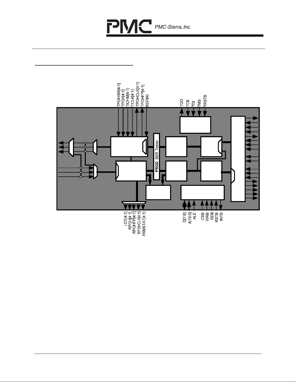
4 S/UNI-CDB BLOCK DIAGRAM
TDATO[4:1]
TOHM [4:1]
TCLK[4:1]
RCLK[4:1]
RDATI[4:1]
ROHM[ 4:1]
SPLT
Transmit ATM
and PLCP Framer
ATMF/SPLR
Receive
ATM and PLCP
Framer
CPPM
PLCP/cell
Perf. Monitor
TXCP_50
Tx
Cell
Processor
RXCP_50
Rx
Cell
Processor
IEEE P1149.1
JTAG Test
Access Port
Microprocessor I/F
TXFF
Tx
4 Cell
FIFO
RXFF
Rx
4 Cell
FIFO
System
I/F
DTCA [4:1]
TDAT[15:0]
TPRTY
TSOC
TCA
TADR[4:0]
TENB
TFCLK
PHY_ADR[2:0]
ATM8
RFCLK
RENB
RADR[4:0]
RCA
RSOC
RPRTY
RDAT[15:0]
DRCA[4:1]
PMC-SIERRA, INC. PROPRIETARY AND CONFIDENTIAL TO PMC-SIERRA INC., AND ITS CUSTOMERS’ INTERNAL USE 10
Page 13

RELEASED
DATASHEET
PMC-2000313 ISSUE 2 SATURN USER NETWORK INTERFACE CELL DELINEATION BLOCK
PM7339 S/UNI-CDB
5 DATASHEET OVERVIEW
The PM7339 S/UNI-CDB is functionally equivalent to a PM7346 S/UNI-QJET
placed in DS3/E3/J2 Framer Bypass mode. The devices are software compatible and
pin compatible. This datasheet provides a complete pin-out description for the S/UNICDB, as well as any differences between these devices. A software initialization
sequence is required for the device to operate properly. This software initialization is
described in section 10.1. For a complete functional and register description, please
refer to the SUNI-QJET Datasheet, PMC-960835.
PMC-SIERRA, INC. PROPRIETARY AND CONFIDENTIAL TO PMC-SIERRA INC., AND ITS CUSTOMERS’ INTERNAL USE 11
Page 14
RELEASED
PM7339 S/UNI-CDB
DATASHEET
PMC-2000313 ISSUE 2 SATURN USER NETWORK INTERFACE CELL DELINEATION BLOCK
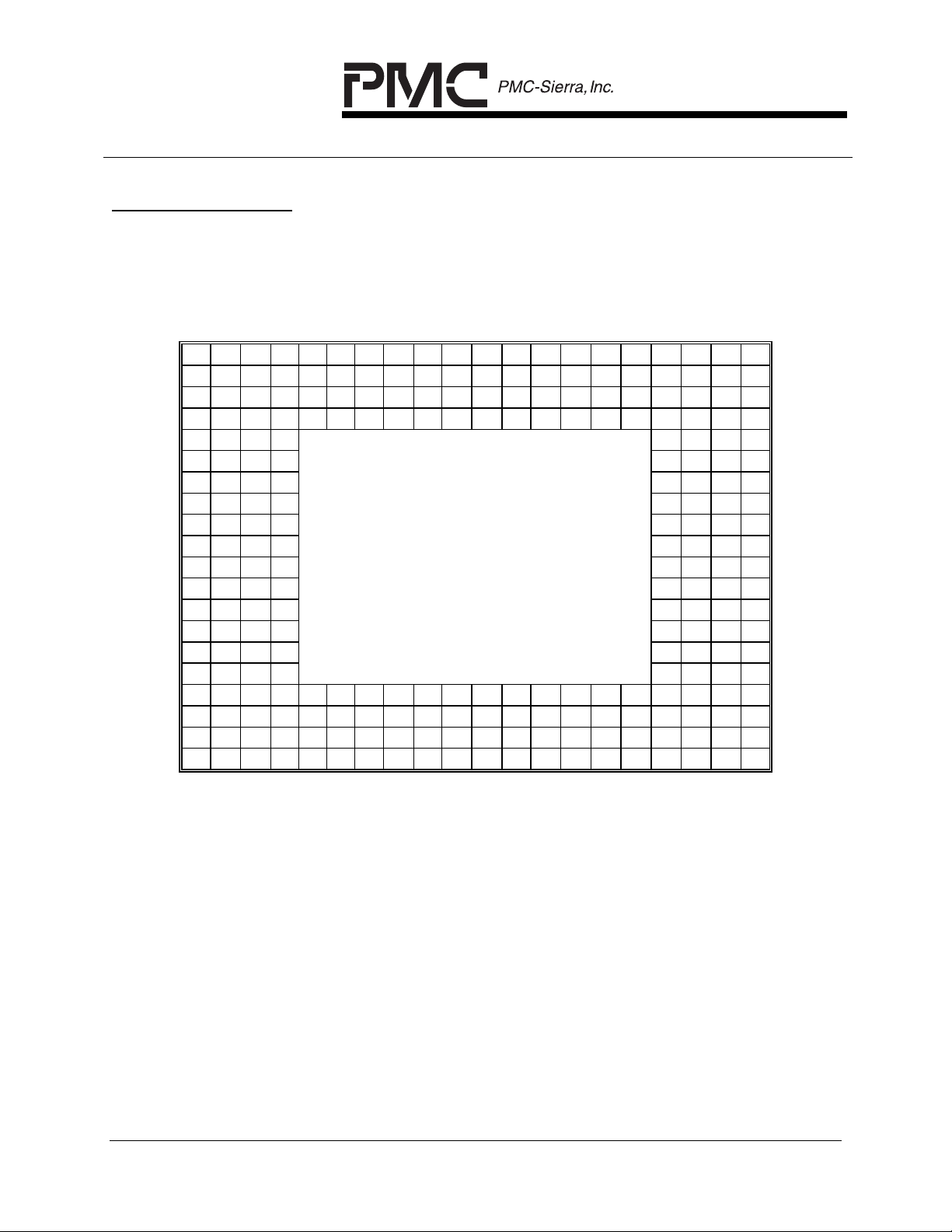
6 PIN DIAGRAM
The S/UNI-CDB is packaged in a 256-pin SBGA package having a body size of
27mm by 27mm and a pin pitch of 1.27 mm.
20 19 18 17 16 15 14 13 12 11 10 9 8 7 6 5 4 3 2 1
A VSS VSS VSS TDAT[10] TDAT[14] D[1] D[5] VSS A[3] A[7] VSS VSS ALE INTB TRSTB TOHM[4] RCLK[4] VSS VSS VSS A
B VSS VDD VDD TDAT[9] TDAT[13] D[0] D[4] A[0] A[2] A[6] A[9] A[10] WRB TDO TCK TCLK[4] TDATO[3] VDD VDD VSS B
C VS S VDD VDD TDAT[7] TDAT[11] TDAT[15] D[2] D[6] A[1] A[5] A[8] CSB RSTB TMS TDATO[4] ROHM[4] TCLK[3] VDD VDD VSS C
D TDAT[3] TDAT[4] TDAT[6] NC TDAT[8] TDAT[12] VDD D[3] D[7] A[ 4] VDD RDB TDI VDD RDATI[4] TOHM[3] BIAS TDATO[2] TCLK[2] RDATI[3] D
E TF CLK TD AT[0] TDA T[2] TDAT[5] TOHM[2] ROHM[3] RDATI[2] ROHM[2] E
F TADR[2] TADR[3] TADR[4] TDAT[1] RCLK[3] RCLK[2] TDATO[1] TOHM[1] F
G TSOC TPRTY TADR[1] VDD VDD TCLK[1] ROHM[1] RCLK[1] G
H BIAS TCA TENB TADR[0] RDATI[1] VSS NC VSS H
J VSS DTCA[2] DTCA[3] DTCA[4] VSS NC NC NC J
K VSS DTCA[1] PHY_ADR[2] VDD
L PHY_ADR[1] PHY_ADR[0] ATM8 DRCA[4] VDD NC NC VSS L
M DRCA[3] DRCA[2] DRCA[1] RSOC VSS NC NC VSS M
N VS S RCA RENB RADR[3] NC NC NC VSS N
P RFCLK RADR[4] RADR[2] VDD VDD VSS NC NC P
R RADR[1] RADR[0] RPRTY RDAT[13] NC NC NC VSS R
T RDA T[15] RDAT[14] RDAT[12] RDAT[9] FRMSTAT[2] REF8KI NC NC T
U RDAT[11] RDAT[10] RDAT[8] B IAS RDAT[6] RDAT[2] VDD TPOHCLK[4] REF8KO[4] VDD RPOHCLK[3] TPOHINS[2] RPOH[2] VDD TPOHCLK[1] RPOHCLK[1] BIAS FRMSTAT[1 ] FRM STAT[3 ] FRMSTA T[4] U
V VSS VDD VDD RDAT[7] RDAT[3] TICLK[4] TPOHINS[4] RPOH[4] TIOHM[3] TPOHCLK[3] RPOH[3] TIOHM[2] TPOHCLK[2] RPOHCLK[2] TIOHM[1] TPOHFP[1] REF8KO[1] VDD VDD VSS V
W VSS VDD VDD RDAT[5] RDAT[1] TIOHM[4] TPOHFP[4] RPOHCLK[4] TPOH[3] TPOHINS[3] LCD[3 ] TICLK[2] TPOH[2] LCD[2] TICLK[1] TPOHINS[1] RPOH[1] VDD VDD VSS W
Y VSS VSS VSS RDAT[4] RDAT[0] TPOH[4] LCD[4] TICLK[3] VSS VSS TPOHFP[3] REF8KO[3] VSS TPOHFP[2] REF8KO[2] TPOH[1] LCD[1] VSS VSS VSS Y
20 19 18 17 16 15 14 13 12 11 10 9 8 7 6 5 4 3 2 1
BOTTOM VIEW
NC VSS VSS NC K
PMC-SIERRA, INC. PROPRIETARY AND CONFIDENTIAL TO PMC-SIERRA INC., AND ITS CUSTOMERS’ INTERNAL USE 12
Page 15

RELEASED
DATASHEET
PMC-2000313 ISSUE 2 SATURN USER NETWORK INTERFACE CELL DELINEATION BLOCK
PM7339 S/UNI-CDB
7 PIN DESCRIPTION
Pin Name Type Pin No. Function
TDATO[4]
TDATO[3]
TDATO[2]
TDATO[1]
Output C6
B4
D3
F2
Transmit Data (TDATO[4:1]). TDATO[4:1]
contains the transmit data stream when
the single-rail (unipolar) output format is
enabled
The TDATO[4:1] pin function selection is
controlled by the TFRM[1:0] and the TUNI
bits in the S/UNI-CDB Transmit
Configuration Registers. TDATO[4:1] is
updated on the falling edge of TCLK[4:1]
by default, and may be configured to be
updated on the rising edge of TCLK[4:1]
through the TCLKINV bit in the S/UNI-CDB
Transmit Configuration Registers. Finally,
TDATO[4:1] can be updated on the rising
edge of TICLK[4:1], enabled by the TICLK
bit in the S/UNI-CDB Transmit
Configuration Registers.
PMC-SIERRA, INC. PROPRIETARY AND CONFIDENTIAL TO PMC-SIERRA INC., AND ITS CUSTOMERS’ INTERNAL USE 13
Page 16
RELEASED
DATASHEET
PMC-2000313 ISSUE 2 SATURN USER NETWORK INTERFACE CELL DELINEATION BLOCK
PM7339 S/UNI-CDB
Pin Name Type Pin No. Function
TOHM[4]
TOHM[3]
TOHM[2]
TOHM[1]
Output A5
D5
E4
F1
Transmit Overhead Mask (TOHM[4:1]).
TOHM[4:1] indicates the position of
overhead bits (non-payload bits) in the
transmission system stream aligned with
TDATO[4:1].
When a PLCP formatted signal is
transmitted, TOHM[4:1] is set to logic 1
once per transmission frame, and
indicates the DS1 or E1 frame alignment.
TOHM[4:1] is a delayed version of the
TIOHM[4:1] input, and indicates the
position of each overhead bit in the
transmission frame. TOHM[4:1] is
updated on the falling edge of TCLK[4:1].
The TOHM[4:1] pin function selection is
controlled by the TFRM[1:0] and the TUNI
bits in the S/UNI-CDB Transmit
Configuration Registers. TOHM[4:1] is
updated on the falling edge of TCLK[4:1]
by default, and may be enabled to be
updated on the rising edge of TCLK[4:1].
This sampling is controlled by the
TCLKINV bit in the S/UNI-CDB Transmit
Configuration Registers. Finally,
TOHM[4:1] can be updated on the rising
edge of TICLK[4:1], enabled by the TICLK
bit in the S/UNI-CDB Transmit
Configuration Registers.
TCLK[4]
TCLK[3]
TCLK[2]
TCLK[1]
Output B5
C4
D2
G3
Transmit Output Clock (TCLK[4:1]).
TCLK[4:1] provides the transmit direction
timing. TCLK[4:1] is a buffered version of
TICLK[4:1] and can be enabled to update
the TDATO[4:1] and TOHM[4:1] outputs on
its rising or falling edge.
PMC-SIERRA, INC. PROPRIETARY AND CONFIDENTIAL TO PMC-SIERRA INC., AND ITS CUSTOMERS’ INTERNAL USE 14
Page 17

RELEASED
DATASHEET
PMC-2000313 ISSUE 2 SATURN USER NETWORK INTERFACE CELL DELINEATION BLOCK
PM7339 S/UNI-CDB
Pin Name Type Pin No. Function
RDATI[4]
RDATI[3]
RDATI[2]
RDATI[1]
ROHM[4]
ROHM[3]
ROHM[2]
ROHM[1]
Input D6
D1
E2
H4
Input C5
E3
E1
G2
Receive Data (RDATI[4:1]). RDATI[4:1]
contains the data stream when the singlerail (unipolar) NRZ input format is enabled.
The RDATI[4:1] pin function selection is
controlled by the RFRM[1:0] bits in the
S/UNI-CDB Configuration Registers.
RDATI[4:1] is sampled on the rising edge
of RCLK[4:1] by default, and may be
enabled to be sampled on the falling edge
of RCLK[4:1]. This sampling is controlled
by the RCLKINV bit in the S/UNI-CDB
Receive Configuration Registers.
Receive Overhead Mask (ROHM[4:1]).
When a DS1 or E1 PLCP or ATM directmapped signal is received, ROHM[4:1] is
pulsed once per transmission frame, and
indicates the DS1 or E1 frame alignment
relative to the RDATI[4:1] data stream.
When an alternate frame-based signal is
received, ROHM[4:1] indicates the position
of each overhead bit in the transmission
frame.
The RLCV/ROHM[4:1] pin function
selection is controlled by the RFRM[1:0]
bits in the S/UNI-CDB Receive
Configuration Registers, and the PLCPEN
bit in the SPLR Configuration register.
RLCV[4:1], and ROHM[4:1] are sampled
on the rising edge of RCLK[4:1] by default,
and may be enabled to be sampled on the
falling edge of RCLK[4:1]. This sampling
is controlled by the RCLKINV bit in the
S/UNI-CDB Receive Configuration
Registers.
RCLK[4]
RCLK[3]
RCLK[2]
RCLK[1]
Input A4
F4
F3
G1
Receive Clock (RCLK[4:1]). RCLK[4:1]
provides the receive direction timing.
RCLK[4:1] is the externally recovered
transmission system baud rate clock that
samples the RDATI[4:1] and
RLCV/ROHM[4:1] inputs on its rising or
falling edge.
PMC-SIERRA, INC. PROPRIETARY AND CONFIDENTIAL TO PMC-SIERRA INC., AND ITS CUSTOMERS’ INTERNAL USE 15
Page 18

RELEASED
DATASHEET
PMC-2000313 ISSUE 2 SATURN USER NETWORK INTERFACE CELL DELINEATION BLOCK
PM7339 S/UNI-CDB
Pin Name Type Pin No. Function
REF8KI Input T3 Reference 8 kHz Input (REF8KI). The
PLCP frame rate is locked to an external 8
kHz reference applied on this input . An
internal phase-frequency detector
compares the transmit PLCP frame rate
with the externally applied 8 kHz reference
and adjusts the PLCP frame rate.
The REF8KI input must transition high
once every 125 µs for correct operation.
The REF8KI input is treated as an
asynchronous signal and must be “glitchfree”. If the LOOPT register bit is logic 1,
the PLCP frame rate is locked to the
RPOHFP[x] signal instead of the REF8KI
input.
TPOHINS[4]
TPOHINS[3]
TPOHINS[2]
TPOHINS[1]
TPOH[4]
TPOH[3]
TPOH[2]
TPOH[1]
Input V14
W11
U9
W5
Input Y15
W12
W8
Y5
Transmit Path Overhead Insertion
(TPOHINS[4:1]). TPOHINS[4:1] controls
the insertion of PLCP overhead octets on
the TPOH[4:1] input. When
TPOHINS[4:1] is logic 1, the associated
overhead bit in the TPOH[4:1] stream is
inserted in the transmit PLCP frame.
When TPOHINS[4:1] is logic 0, the PLCP
path overhead bit is generated and
inserted internally. TPOHINS[4:1] is
sampled on the rising edge of
TPOHCLK[4:1].
Transmit PLCP Overhead Data
(TPOH[4:1]). TPOH[4:1] contains the
PLCP path overhead octets (Zn, F1, B1,
G1, M1, M2, and C1) which may be
inserted in the transmit PLCP frame. The
octet data on TPOH[4:1] is shifted in order
from the most significant bit (bit 1) to the
least significant bit (bit 8). TPOH[4:1] is
sampled on the rising edge of
TPOHCLK[4:1].
PMC-SIERRA, INC. PROPRIETARY AND CONFIDENTIAL TO PMC-SIERRA INC., AND ITS CUSTOMERS’ INTERNAL USE 16
Page 19

RELEASED
DATASHEET
PMC-2000313 ISSUE 2 SATURN USER NETWORK INTERFACE CELL DELINEATION BLOCK
PM7339 S/UNI-CDB
Pin Name Type Pin No. Function
TCELL[4]
TCELL[3]
TCELL[2]
TCELL[1]
TPOHCLK[4]
TPOHCLK[3]
TPOHCLK[2]
TPOHCLK[1]
TIOHM[4]
TIOHM[3]
TIOHM[2]
TIOHM[1]
Output W14
Y10
Y7
V5
Output U13
V11
V8
U6
Input W15
V12
V9
V6
Transmit Cell Indication (TCELL[4:1]).
TCELL[x] is valid when the TCELL bit in
the S/UNI-CDB Misc. register (09BH,
19BH, 29BH, 39BH) is set. TCELL[x]
pulses once for every cell (idle or
assigned) transmitted. TCELL[x] is
updated using timing derived from the
transmit input clock (TICLK[x]), and is
active for a minimum of 8 TICLK[x] periods
(or 8 RCLK[x] periods if loop-timed).
Transmit PLCP Overhead Clock
(TPOHCLK[4:1]). TPOHCLK[4:1] is active
when PLCP processing is enabled.
TPOHCLK[4:1] is nominally a 26.7 kHz
clock for a DS1 PLCP frame and a 33.7
kHz clock for an E1 based PLCP frame.
TPOHFP[4:1] is updated on the falling
edge of TPOHCLK[4:1]. TPOH[4:1], and
TPOHINS[4:1] are sampled on the rising
edge of TPOHCLK[4:1].
Transmit Input Overhead Mask
(TIOHM[4:1]). TIOHM[4:1] indicates the
position of overhead bits when not
configured for DS1 or E1 transmission
system streams. TIOHM[4:1] is delayed
internally to produce the TOHM[4:1]
output. When configured for operation
over a DS1 or an E1 transmission system
sublayer, TIOHM[4:1] is not required, and
should be set to logic 0. When configured
for other transmission systems,
TIOHM[4:1] is set to logic 1 for each
overhead bit position. TIOHM[4:1] is set to
logic 0 if the transmission system contains
no overhead bits. TIOHM[4:1] is sampled
on the rising edge of TICLK[4:1].
PMC-SIERRA, INC. PROPRIETARY AND CONFIDENTIAL TO PMC-SIERRA INC., AND ITS CUSTOMERS’ INTERNAL USE 17
Page 20

RELEASED
DATASHEET
PMC-2000313 ISSUE 2 SATURN USER NETWORK INTERFACE CELL DELINEATION BLOCK
PM7339 S/UNI-CDB
Pin Name Type Pin No. Function
TICLK[4]
TICLK[3]
TICLK[2]
TICLK[1]
RPOHFP[4]
RPOHFP[3]
RPOHFP[2]
RPOHFP[1]
Input V15
Y13
W9
W6
Output U12
Y9
Y6
V4
Transmit Input Clock (TICLK[4:1]).
TICLK[4:1] provides the transmit direction
timing. TICLK[4:1] is the externally
generated transmission system baud rate
clock. It is internally buffered to produce
the transmit clock output, TCLK[4:1], and
can be enabled to update the TDATO[4:1]
and TOHM[4:1] outputs on the TICLK[4:1]
rising edge. The TICLK[4:1] maximum
frequency is 52 MHz.
Receive PLCP Overhead Frame Position
(RPOHFP[4:1]). RPOHFP[4:1] locates the
individual PLCP path overhead bits in the
receive overhead data stream, RPOH[4:1].
RPOHFP[4:1] is logic 1 while bit 1 (the
most significant bit) of the path user
channel octet (F1) is present in the
RPOH[4:1] stream. RPOHFP[4:1] is
updated on the falling edge of
RPOHCLK[4:1]. RPOHFP[4:1] is available
when the PLCPEN register bit is logic 1 in
the SPLR Configuration Register.
RPOH[4]
RPOH[3]
RPOH[2]
RPOH[1]
Output V13
V10
U8
W4
Receive PLCP Overhead Data
(RPOH[4:1]). RPOH[4:1] contains the
PLCP path overhead octets (Zn, F1, B1,
G1, M1, M2, and C1) extracted from the
received PLCP frame when the PLCP
layer is in-frame. When the PLCP layer is
in the loss of frame state, RPOH[4:1] is
forced to all ones. The octet data on
RPOH[4:1] is shifted out in order from the
most significant bit (bit 1) to the least
significant bit (bit 8). RPOH[4:1] is
updated on the falling edge of
RPOHCLK[4:1].
PMC-SIERRA, INC. PROPRIETARY AND CONFIDENTIAL TO PMC-SIERRA INC., AND ITS CUSTOMERS’ INTERNAL USE 18
Page 21

RELEASED
DATASHEET
PMC-2000313 ISSUE 2 SATURN USER NETWORK INTERFACE CELL DELINEATION BLOCK
PM7339 S/UNI-CDB
Pin Name Type Pin No. Function
RPOHCLK[4]
RPOHCLK[3]
RPOHCLK[2]
RPOHCLK[1]
LCD[4]
LCD[3]
LCD[2]
LCD[1]
FRMSTAT[4]
FRMSTAT[3]
FRMSTAT[2]
FRMSTAT[1]
Output W13
U10
V7
U5
Output Y14
W10
W7
Y4
Output U1
U2
T4
U3
Receive PLCP Overhead Clock
(RPOHCLK[4:1]). RPOHCLK[4:1] is active
when PLCP processing is enabled. The
frequency of this signal depends on the
selected PLCP format. RPOHCLK[4:1] is
nominally a 26.7 kHz clock for a DS1
PLCP frame and a 33.7 kHz clock for an
E1 based PLCP frame. RPOHFP[4:1] and
RPOH[4:1] are updated on the falling edge
of RPOHCLK[4:1].
Loss of Cell Delineation (LCD[4:1]).
LCD[4:1] is an active high signal which is
asserted while the ATM cell processor has
detected a Loss of Cell Delineation defect.
Framer Status (FRMSTAT[4:1]).
FRMSTAT[4:1] is an active high signal
which can be configured to show when the
PLCP framer has detected certain
conditions. The FRMSTAT[4:1] outputs
can be programmed via the STATSEL[2:0]
bits in the S/UNI-CDB Configuration 2
Register to indicate: PLCP Loss of Frame,
PLCP Out of Frame, AIS, and Loss of
Signal. FRMSTAT[4:1] should be treated
as a glitch free asynchronous signal.
ATM8 Input L18 ATM Interface Bus Width Selection
(ATM8). The ATM8 input pin determines
whether the S/UNI-CDB works with a 8-bit
wide interface (RDAT[7:0] and TDAT[7:0])
or a 16-bit wide interface (RDAT[15:0] and
TDAT[15:0]). If ATM8 is set to logic 1,
then the 8-bit wide interface is chosen. If
ATM8 is set to logic 0, then the 16-bit wide
interface is chosen.
PMC-SIERRA, INC. PROPRIETARY AND CONFIDENTIAL TO PMC-SIERRA INC., AND ITS CUSTOMERS’ INTERNAL USE 19
Page 22
RELEASED
DATASHEET
PMC-2000313 ISSUE 2 SATURN USER NETWORK INTERFACE CELL DELINEATION BLOCK
PM7339 S/UNI-CDB
Pin Name Type Pin No. Function
TDAT[15]
TDAT[14]
TDAT[13]
TDAT[12]
TDAT[11]
TDAT[10]
TDAT[9]
TDAT[8]
TDAT[7]
TDAT[6]
TDAT[5]
TDAT[4]
TDAT[3]
TDAT[2]
TDAT[1]
Input C15
A16
B16
D15
C16
A17
B17
D16
C17
D18
E17
D19
D20
E18
F17
Transmit Cell Data Bus (TDAT[15:0]). This
bus carries the ATM cell octets that are
written to the selected transmit FIFO.
TDAT[15:0] is sampled on the rising edge
of TFCLK and is considered valid only
when TENB is simultaneously asserted
and the S/UNI-CDB has been selected via
the TADR[4:2] and PHY_ADR[2:0] inputs.
The S/UNI-CDB can be configured to
operate with an 8-bit wide or 16-bit wide
ATM data interface via the ATM8 input pin.
When configured for the 8-bit wide
interface, TDAT[15:8] are not used and
should be tied to ground.
TDAT[0]
E19
PMC-SIERRA, INC. PROPRIETARY AND CONFIDENTIAL TO PMC-SIERRA INC., AND ITS CUSTOMERS’ INTERNAL USE 20
Page 23

RELEASED
DATASHEET
PMC-2000313 ISSUE 2 SATURN USER NETWORK INTERFACE CELL DELINEATION BLOCK
PM7339 S/UNI-CDB
Pin Name Type Pin No. Function
TPRTY Input G19 Transmit bus parity (TPRTY). The
transmit parity (TPRTY) signal indicates
the parity of the TDAT[15:0] or TDAT[7:0]
bus. If configured for the 8-bit bus (via the
ATM8 input pin), then parity is calculated
over TDAT[7:0]. If configured for the 16-bit
bus, then parity is calculated over
TDAT[15:0].
A parity error is indicated by a status bit
and a maskable interrupt. Cells with parity
errors are inserted in the transmit stream,
so the TPRTY input may be unused.
Odd or even parity selection is made using
the TPTYP register bit. TPRTY is sampled
on the rising edge of TFCLK and is
considered valid only when TENB is
simultaneously asserted and the
S/UNI-CDB has been selected via the
TADR[4:0] and PHY_ADR[2:0] inputs.
TSOC Input G20 Transmit Start of Cell (TSOC). The
transmit start of cell (TSOC) signal marks
the start of cell on the TDAT bus. When
TSOC is high, the first word of the cell
structure is present on the TDAT bus. It is
not necessary for TSOC to be present for
each cell. An interrupt may be generated
if TSOC is high during any word other than
the first word of the cell structure. TSOC
is sampled on the rising edge of TFCLK
and is considered valid only when TENB is
simultaneously asserted and the
S/UNI-CDB has been selected via the
TADR[4:2] and PHY_ADR[2:0] inputs.
PMC-SIERRA, INC. PROPRIETARY AND CONFIDENTIAL TO PMC-SIERRA INC., AND ITS CUSTOMERS’ INTERNAL USE 21
Page 24
RELEASED
DATASHEET
PMC-2000313 ISSUE 2 SATURN USER NETWORK INTERFACE CELL DELINEATION BLOCK
PM7339 S/UNI-CDB
Pin Name Type Pin No. Function
TENB Input H18 Transmit Multi-Phy Write Enable (TENB).
The TENB signal is an active low input
which is used along with the TADR[4:0]
inputs to initiate writes to the transmit
FIFOs. When sampled low using the
rising edge of TFCLK, the word on the
TDAT bus is written into the transmit FIFO
selected by the TADR[4:0] address bus.
When sampled high using the rising edge
of TFCLK, no write is performed, but the
TADR[4:0] address is latched to identify
the transmit FIFO to be accessed. A
complete 53 octet cell must be written to
the transmit FIFO before it is inserted into
the transmit stream. Idle cells are inserted
when a complete cell is not available.
TADR[4]
TADR[3]
TADR[2]
TADR[1]
TADR[0]
Input F18
F19
F20
G18
H17
Transmit Address (TADR[4:0]). The
TADR[4:0] bus is used to select the FIFO
(and hence port) that is written to using the
TENB signal and the FIFO whose cellavailable signal is visible on the TCA
output. TADR[4:0] is sampled on the
rising edge of TFCLK together with TENB.
Note that the null-PHY address 1FH is an
invalid address and will not be identified to
any port on the S/UNI-CDB.
PMC-SIERRA, INC. PROPRIETARY AND CONFIDENTIAL TO PMC-SIERRA INC., AND ITS CUSTOMERS’ INTERNAL USE 22
Page 25
RELEASED
DATASHEET
PMC-2000313 ISSUE 2 SATURN USER NETWORK INTERFACE CELL DELINEATION BLOCK
PM7339 S/UNI-CDB
Pin Name Type Pin No. Function
TCA Output H19 Transmit Multi-Phy Cell Available (TCA).
The TCA signal indicates when a cell is
available in the transmit FIFO for the port
selected by TADR[4:0]. When high, TCA
indicates that the corresponding transmit
FIFO is not full and a complete cell may be
written. When TCA goes low, it can be
configured to indicate either that the
corresponding transmit FIFO is near full or
that the corresponding transmit FIFO is
full. TCA will transition low on the rising
edge of TFCLK which samples Payload
byte 43 (TCALEVEL0=0) or 47
(TCALEVEL0=1) for the 8-bit interface
(ATM8=1), or the rising edge of TFCLK
which samples Payload word 19
(TCALEVEL0=0) or 23 (TCALEVEL0=1)
for the 16-bit interface (ATM8=0) if the
PHY being polled is the same as the PHY
in use. To reduce FIFO latency, the FIFO
depth at which TCA indicates "full" can be
set to one, two, three or four cells. Note
that regardless of what fill level TCA is set
to indicate "full" at, the transmit cell
processor can store 4 complete cells.
TCA is tri-stated when either the null-PHY
address (1FH) or an address not matching
the address space set by PHY_ADR[2:0]
is latched (by TFCLK) from the TADR[4:2]
inputs.
The polarity of TCA (with respect the the
description above) is inverted when the
TCAINV register bit is set to logic 1.
TFCLK Input E20 Transmit FIFO Write Clock (TFCLK). This
signal is used to write ATM cells to the four
cell transmit FIFOs. TFCLK cycles at a 52
MHz or lower instantaneous rate.
Please note that the TFCLK input is not 5
V tolerant, it is a 3.3 V only input pin.
PMC-SIERRA, INC. PROPRIETARY AND CONFIDENTIAL TO PMC-SIERRA INC., AND ITS CUSTOMERS’ INTERNAL USE 23
Page 26

RELEASED
DATASHEET
PMC-2000313 ISSUE 2 SATURN USER NETWORK INTERFACE CELL DELINEATION BLOCK
PM7339 S/UNI-CDB
Pin Name Type Pin No. Function
DTCA[4]
DTCA[3]
DTCA[2]
DTCA[1]
Output J17
J18
J19
K19
Direct Access Transmit Cell Available
(DTCA[4:1]). These output signals
indicate when a cell is available in the
transmit FIFO for the corresponding port.
When high, DTCA[x] indicates that the
corresponding transmit FIFO is not full and
a complete cell may be written. DTCA[x]
can be configured to indicate either that
the corresponding transmit FIFO is near
full and can accept no more than four
writes or that the corresponding transmit
FIFO is full. DTCA[x] will thus transition
low on the rising edge of TFLCK which
samples Payload byte 43 (TCALEVEL0=0)
or 47 (TCALEVEL0=1) for the 8-bit
interface (ATM8=1), or the rising edge of
TFCLK which samples Payload word 19
(TCALEVEL0=0) or 23 (TCALEVEL0=1)
for the 16-bit interface (ATM8=0). To
reduce FIFO latency, the FIFO depth at
which DTCA[x] indicates "full" can be set
to one, two, three or four cells. Note that
regardless of what fill level DTCA[x] is set
to indicate "full" at, the transmit cell
processor can store 4 complete cells.
The polarity of DTCA[x] (with respect the
the description above) is inverted when
the TCAINV register bit is set to logic 1.
The DTCA[4:1] outputs can be used to
support Utopia Direct Access mode.
PMC-SIERRA, INC. PROPRIETARY AND CONFIDENTIAL TO PMC-SIERRA INC., AND ITS CUSTOMERS’ INTERNAL USE 24
Page 27

RELEASED
DATASHEET
PMC-2000313 ISSUE 2 SATURN USER NETWORK INTERFACE CELL DELINEATION BLOCK
PM7339 S/UNI-CDB
Pin Name Type Pin No. Function
RDAT[15]
RDAT[14]
RDAT[13]
RDAT[12]
RDAT[11]
RDAT[10]
RDAT[9]
RDAT[8]
RDAT[7]
RDAT[6]
RDAT[5]
RDAT[4]
RDAT[3]
RDAT[2]
RDAT[1]
Output T20
T19
R17
T18
U20
U19
T17
U18
V17
U16
W17
Y17
V16
U15
W16
Receive Cell Data Bus (RDAT[15:0]). This
bus carries the ATM cell octets that are
read from the receive ATM FIFO selected
by RADR[4:0]. RDAT[15:0] is tri-stated
when RENB is high. RDAT[15:0] is
updated on the rising edge of RFCLK.
The S/UNI-CDB can be configured to
operate with an 8-bit wide or 16-bit wide
ATM data interface via the ATM8 input pin.
RDAT[15:8] will remain tri-stated if ATM8 is
set to logic 1.
RDAT[15:0] is tri-stated when either the
null-PHY address (1FH) or an address not
matching the address space set by
PHY_ADR[2:0] is latched from the
RADR[4:2] inputs when RENB is high.
RDAT[0]
Y16
RPRTY Output R18 Receive Parity (RPRTY). The receive
parity (RPRTY) signal indicates the parity
of the RDAT bus.
The S/UNI-CDB can be configured to
operate with an 8-bit wide or 16-bit wide
ATM data interface via the ATM8 input pin.
In the 8-bit mode, RPRTY reflects the
parity of RDAT[7:0]. In the 16-bit mode,
RPRTY reflects the parity of RDAT[15:0].
Odd or even parity selection is made using
the RXPTYP register bit.
RPRTY is tri-stated when either the nullPHY address (1FH) or an address not
matching the address space set by
PHY_ADR[2:0] is latched from the
RADR[4:2] inputs when RENB is high.
PMC-SIERRA, INC. PROPRIETARY AND CONFIDENTIAL TO PMC-SIERRA INC., AND ITS CUSTOMERS’ INTERNAL USE 25
Page 28

RELEASED
DATASHEET
PMC-2000313 ISSUE 2 SATURN USER NETWORK INTERFACE CELL DELINEATION BLOCK
PM7339 S/UNI-CDB
Pin Name Type Pin No. Function
RSOC Output M17 Receive Start of Cell (RSOC). This signal
marks the start of cell on the RDAT bus.
RSOC marks the start of the cell on the
RDAT bus.
RSOC is tri-stated when either the nullPHY address (1FH) or an address not
matching the address space set by
PHY_ADR[2:0] is latched from the
RADR[4:0] inputs when RENB is high.
RENB Input N18 Receive Multi-Phy Read Enable (RENB).
The RENB signal is used to initiate reads
from the receive FIFOs. When sampled
low using the rising edge of RFCLK, a byte
is read (if one is available) from the
receive FIFO selected by the RADR[4:0]
address bus and output on the RDAT bus.
When sampled high using the rising edge
of RFCLK, no read is performed and
RDAT[15:0], RPRTY, and RSOC are tristated, and the address on RADR[4:0] is
latched to select the device or port for the
next ATM FIFO access. RENB must
operate in conjunction with RFCLK to
access the FIFOs at a high enough rate to
prevent FIFO overflows. The ATM layer
device may de-assert RENB at anytime it
is unable to accept another byte.
RADR[4]
RADR[3]
RADR[2]
RADR[1]
Input P19
N17
P18
R20
Receive Address (RADR[4:0]). The
RADR[4:1] signal is used to select the
FIFO (and hence port) that is read from
using the RENB signal and the FIFO
whose cell-available signal is visible on the
RCA output. RADR[4:0] is sampled on the
RADR[0]
R19
rising edge of RFCLK together with RENB.
Note that the null-PHY address 1FH is an
invalid address and will not be identified to
any port on the S/UNI-CDB.
PMC-SIERRA, INC. PROPRIETARY AND CONFIDENTIAL TO PMC-SIERRA INC., AND ITS CUSTOMERS’ INTERNAL USE 26
Page 29

RELEASED
DATASHEET
PMC-2000313 ISSUE 2 SATURN USER NETWORK INTERFACE CELL DELINEATION BLOCK
PM7339 S/UNI-CDB
Pin Name Type Pin No. Function
RCA Output N19 Receive Multi-Phy Cell Available (RCA).
The RCA signal indicates when a cell is
available in the receive FIFO for the port
selected by RADR[4:0]. RCA can be
configured to be de-asserted when either
zero or four bytes remain in the
selected/addressed FIFO. RCA will thus
transition low on the rising edge of RFCLK
after Payload byte 48 (RCALEVEL0=1) or
43 (RCALEVEL0=0) is output for the 8-bit
interface (ATM8=1), or after Payload word
24 (RCALEVEL0=1) or 19
(RCALEVEL0=0) is output for the 16-bit
interface (ATM8=0) if the PHY being polled
is the same as the PHY in use.
RCA is tri-stated when either the null-PHY
address (1FH) or an address not matching
the address space set by PHY_ADR[2:0]
is latched (by RFCLK) from the RADR[4:2]
inputs.
The polarity of RCA (with respect to the
description above) is inverted when the
RCAINV register bit is set to logic 1.
RFCLK Input P20 Receive FIFO Read Clock (RFCLK). This
signal is used to read ATM cells from the
receive FIFOs. RFCLK must cycle at a 52
MHz or lower instantaneous rate, but at a
high enough rate to avoid FIFO overflows.
Please note that the RFCLK input is not 5
V tolerant, it is a 3.3 V only input pin.
PMC-SIERRA, INC. PROPRIETARY AND CONFIDENTIAL TO PMC-SIERRA INC., AND ITS CUSTOMERS’ INTERNAL USE 27
Page 30

RELEASED
DATASHEET
PMC-2000313 ISSUE 2 SATURN USER NETWORK INTERFACE CELL DELINEATION BLOCK
PM7339 S/UNI-CDB
Pin Name Type Pin No. Function
DRCA[4]
DRCA[3]
DRCA[2]
DRCA[1]
PHY_ADR[2]
PHY_ADR[1]
PHY_ADR[0]
Output L17
M20
M19
M18
Input K18
L20
L19
Direct Access Receive Cell Available
(DRCA[4:1]). These output signals
indicate when a cell is available in the
receive FIFO for the corresponding port.
DRCA[4:1] can be configured to be deasserted when either zero or four bytes
remain in the FIFO. DRCA[4:1] will thus
transition low on the rising edge of RFCLK
after Payload byte 48 (RCALEVEL0=1) or
43 (RCALEVEL0=0) is output for the 8-bit
interface (ATM8=1), or after Payload word
24 (RCALEVEL0=1) or 19
(RCALEVEL0=0) is output for the 16-bit
interface (ATM8=0).
The DRCA[4:1] outputs can be used to
support Utopia Direct Access mode.
Device Identification Address
(PHY_ADR[2:0]). The PHY_ADR[2:0]
inputs are the most-significant bits of the
address space which this S/UNI-CDB
occupies. When the PHY_ADR[2:0]
inputs match the TADR[4:2] or RADR[4:2]
inputs, then one of the four quadrants (as
determined by the TADR[1:0] or
RADR[1:0] inputs) in this S/UNI-CDB is
selected for transmit or receive ATM
access.
Note that the null-PHY address 1FH is an
invalid address and will not be identified to
any port on the S/UNI-CDB.
CSB Input C9 Active low Chip Select (CSB). This signal
must be low to enable S/UNI-CDB register
accesses. If CSB is not used, (RDB and
WRB determine register reads and writes)
then it should be tied to an inverted
version of RSTB.
PMC-SIERRA, INC. PROPRIETARY AND CONFIDENTIAL TO PMC-SIERRA INC., AND ITS CUSTOMERS’ INTERNAL USE 28
Page 31

RELEASED
DATASHEET
PMC-2000313 ISSUE 2 SATURN USER NETWORK INTERFACE CELL DELINEATION BLOCK
PM7339 S/UNI-CDB
Pin Name Type Pin No. Function
WRB Input B8 Active low Write Strobe (WRB). This signal
is pulsed low to enable a S/UNI-CDB
register write access. The D[7:0] bus is
clocked into the addressed register on the
rising edge of WRB while CSB is low.
RDB Input D9 Active low Read Enable (RDB). This signal
is pulsed low to enable a S/UNI-CDB
register read access. The S/UNI-CDB
drives the D[7:0] bus with the contents of
the addressed register while RDB and
CSB are both low.
D[7]
D[6]
D[5]
D[4]
D[3]
D[2]
D[1]
D[0]
A[10]
A[9]
A[8]
A[7]
A[6]
A[5]
A[4]
I/O D12
C13
A14
B14
D13
C14
A15
B15
Input B9
B10
C10
A11
B11
C11
D11
Bi-directional Data Bus (D[7:0]). The bidirectional data bus D[7:0] is used during
S/UNI-CDB register read and write
accesses.
Address Bus (A[10:0]). The address bus
A[10:0] selects specific registers during
S/UNI-CDB register accesses.
A[3]
A[2]
A[1]
A[0]
PMC-SIERRA, INC. PROPRIETARY AND CONFIDENTIAL TO PMC-SIERRA INC., AND ITS CUSTOMERS’ INTERNAL USE 29
A12
B12
C12
B13
Page 32

RELEASED
DATASHEET
PMC-2000313 ISSUE 2 SATURN USER NETWORK INTERFACE CELL DELINEATION BLOCK
PM7339 S/UNI-CDB
Pin Name Type Pin No. Function
RSTB Input C8 Active low Reset (RSTB). This signal is set
low to asynchronously reset the
S/UNI-CDB. RSTB is a Schmitt-trigger
input with an integral pull-up resistor.
ALE Input A8 Address Latch Enable (ALE). The
address latch enable (ALE) is active-high
and latches the address bus A[10:0] when
low. When ALE is high, the internal
address latches are transparent. It allows
the S/UNI-CDB to interface to a
multiplexed address/data bus. ALE has an
integral pull-up resistor.
INTB Output A7 Active low Open-Drain Interrupt (INTB).
This signal goes low when an unmasked
interrupt event is detected on any of the
internal interrupt sources. Note that INTB
will remain low until all active, unmasked
interrupt sources are acknowledged at
their source.
TCK Input B6 Test Clock (TCK). This signal provides
timing for test operations that can be
carried out using the IEEE P1149.1 test
access port.
TMS Input C7 Test Mode Select (TMS). This signal
controls the test operations that can be
carried out using the IEEE P1149.1 test
access port. TMS is sampled on the rising
edge of TCK. TMS has an integral pull up
resistor.
TDI Input D8 Test Data Input (TDI). This signal carries
test data into the S/UNI-CDB via the IEEE
P1149.1 test access port. TDI is sampled
on the rising edge of TCK. TDI has an
integral pull up resistor.
PMC-SIERRA, INC. PROPRIETARY AND CONFIDENTIAL TO PMC-SIERRA INC., AND ITS CUSTOMERS’ INTERNAL USE 30
Page 33

RELEASED
DATASHEET
PMC-2000313 ISSUE 2 SATURN USER NETWORK INTERFACE CELL DELINEATION BLOCK
PM7339 S/UNI-CDB
Pin Name Type Pin No. Function
TDO Output B7 Test Data Output (TDO). This signal
carries test data out of the S/UNI-CDB via
the IEEE P1149.1 test access port. TDO
is updated on the falling edge of TCK.
TDO is a tri-state output which is inactive
except when scanning of data is in
progress.
TRSTB Input A6 Active low Test Reset (TRSTB). This
signal provides an asynchronous
S/UNI-CDB test access port reset via the
IEEE P1149.1 test access port. TRSTB is
a Schmitt triggered input with an integral
pull up resistor. TRSTB must be asserted
during the power up sequence.
BIAS Input H20
U17
D4
U4
Note that if not used, TRSTB must be
connected to the RSTB input.
+5V Bias (BIAS). When tied to +5V, the
BIAS input is used to bias the wells in the
input and I/O pads so that the pads can
tolerate 5V on their inputs without forward
biasing internal ESD protection devices.
When tied to VDD, the inputs and bidirectional inputs will only tolerate input
levels up to VDD.
PMC-SIERRA, INC. PROPRIETARY AND CONFIDENTIAL TO PMC-SIERRA INC., AND ITS CUSTOMERS’ INTERNAL USE 31
Page 34

RELEASED
DATASHEET
PMC-2000313 ISSUE 2 SATURN USER NETWORK INTERFACE CELL DELINEATION BLOCK
PM7339 S/UNI-CDB
Pin Name Type Pin No. Function
VDD[1]
VDD[2]
VDD[3]
VDD[4]
VDD[5]
VDD[6]
VDD[7]
VDD[8]
VDD[9]
VDD[10]
VDD[11]
VDD[12]
VDD[13]
VDD[14]
VDD[15]
Power B2
B3
B18
B19
C2
C3
C18
C19
D7
D10
D14
G4
G17
K17
L4
DC Power. The DC Power pins should be
connected to a well-decoupled +3.3V DC
supply.
VDD[16]
VDD[17]
VDD[18]
VDD[19]
VDD[20]
VDD[21]
VDD[22]
VDD[23]
VDD[24]
VDD[25]
VDD[26]
VDD[27]
VDD[28]
P4
P17
U7
U11
U14
V2
V3
V18
V19
W2
W3
W18
W19
PMC-SIERRA, INC. PROPRIETARY AND CONFIDENTIAL TO PMC-SIERRA INC., AND ITS CUSTOMERS’ INTERNAL USE 32
Page 35

RELEASED
DATASHEET
PMC-2000313 ISSUE 2 SATURN USER NETWORK INTERFACE CELL DELINEATION BLOCK
PM7339 S/UNI-CDB
Pin Name Type Pin No. Function
VSS[1]
VSS[2]
VSS[3]
VSS[4]
VSS[5]
VSS[6]
VSS[7]
VSS[8]
VSS[9]
VSS[10]
VSS[11]
VSS[12]
VSS[13]
VSS[14]
VSS[15]
Ground A1
A2
A3
A9
A10
A13
A18
A19
A20
B1
B20
C1
C20
H1
H3
DC Ground. The DC Ground pins should
be connected to GND.
VSS[16]
VSS[17]
VSS[18]
VSS[19]
VSS[20]
VSS[21]
VSS[22]
VSS[23]
VSS[24]
VSS[25]
VSS[26]
VSS[27]
VSS[28]
VSS[29]
J4
J20
K2
K3
K20
L1
M1
M4
N1
N20
P3
R1
V1
V20
PMC-SIERRA, INC. PROPRIETARY AND CONFIDENTIAL TO PMC-SIERRA INC., AND ITS CUSTOMERS’ INTERNAL USE 33
Page 36

RELEASED
DATASHEET
PMC-2000313 ISSUE 2 SATURN USER NETWORK INTERFACE CELL DELINEATION BLOCK
PM7339 S/UNI-CDB
Pin Name Type Pin No. Function
VSS[30]
VSS[31]
VSS[32]
VSS[33]
VSS[34]
VSS[35]
VSS[36]
VSS[37]
VSS[38]
VSS[39]
VSS[40]
Ground W1
W20
Y1
Y2
Y3
Y8
Y11
Y12
Y18
Y19
Y20
DC Ground. The DC Ground pins should
be connected to GND.
PMC-SIERRA, INC. PROPRIETARY AND CONFIDENTIAL TO PMC-SIERRA INC., AND ITS CUSTOMERS’ INTERNAL USE 34
Page 37

RELEASED
DATASHEET
PMC-2000313 ISSUE 2 SATURN USER NETWORK INTERFACE CELL DELINEATION BLOCK
PM7339 S/UNI-CDB
Pin Name Type Pin No. Function
NC No
connect
D17
H2
J1
J2
J3
K1
K4
L2
L3
M2
M3
N2
N3
N4
P1
No connect
P2
R2
R3
R4
T1
T2
Notes on Pin Description:
1. All S/UNI-CDB inputs and bi-directionals present minimum capacitive loading
and operate at TTL logic levels.
2. All S/UNI-CDB outputs and bi-directionals have at least 3 mA drive capability.
The data bus outputs, D[7:0], have 3 mA drive capability. The FIFO interface
outputs, RDAT[15:0], RPRTY, RCA, DRCA[4:1], RSOC, TCA, and DTCA[4:1],
have 12 mA drive capability. The outputs TCLK[4:1], TDATO[4:1],
TOHM[4:1], TPOHFP[4:1], LCD[4:1], RPOH[4:1], RPOHCLK[4:1], and
PMC-SIERRA, INC. PROPRIETARY AND CONFIDENTIAL TO PMC-SIERRA INC., AND ITS CUSTOMERS’ INTERNAL USE 35
Page 38

RELEASED
DATASHEET
PMC-2000313 ISSUE 2 SATURN USER NETWORK INTERFACE CELL DELINEATION BLOCK
PM7339 S/UNI-CDB
RPOHFP[4:1] have 6 mA drive capability. All other outputs have 3 mA drive
capability.
3. Inputs RSTB, ALE, TMS, TDI and TRSTB have internal pull-up resistors.
4. RSTB, TRSTB, TMS, TDI, TCK, REF8KI, TFCLK, RFCLK, TICLK[4:1], and
RCLK[4:1] are schmitt trigger input pads.
5. RFCLK and TFCLK are 3.3 V only input pins – they are not 5 V tolerant.
Connecting a 5 V signal to these inputs may result in damage to the part.
6. The VSS [42:1] ground pins are not internally connected together. Failure to
connect these pins externally may cause malfunction or damage the
S/UNI-CDB.
7. The VDD[28:1] power pins are not internally connected together. Failure to
connect these pins externally may cause malfunction or damage the device.
These power supply connections must all be utilized and must all connect to
a common +3.3 V or ground rail, as appropriate.
8. During power-up and power-down, the voltage on the BIAS pin must be kept
equal to or greater than the voltage on the VDD [28:1] pins, to avoid damage
to the device.
PMC-SIERRA, INC. PROPRIETARY AND CONFIDENTIAL TO PMC-SIERRA INC., AND ITS CUSTOMERS’ INTERNAL USE 36
Page 39

RELEASED
DATASHEET
PMC-2000313 ISSUE 2 SATURN USER NETWORK INTERFACE CELL DELINEATION BLOCK
PM7339 S/UNI-CDB
8 FUNCTIONAL DESCRIPTION
8.1 SPLR PLCP Layer Receiver
The PLCP Layer Receiver (SPLR) Block integrates circuitry to support DS1 and
E1 PLCP frame processing. The SPLR provides framing for PLCP based
transmission formats.
The SPLR frames to DS1 and E1 based PLCP frames with maximum average
reframe times of 635 µs and 483 µs respectively. Framing is declared (out of
frame is removed) upon finding 2 valid, consecutive sets of framing (A1 and A2)
octets and 2 valid and sequential path overhead identifier (POHID) octets. While
framed, the A1, A2, and POHID octets are examined. OOF is declared when an
error is detected in both the A1 and A2 octets or when 2 consecutive POHID
octets are found in error. LOF is declared when an OOF state persists for more
than 25 ms, 1 ms, 20 ms, or 1 ms for DS1 and E1 PLCP formats respectively. If
the OOF events are intermittent, the LOF counter is decremented at a rate 1/10
(E1, DS1 PLCP) of the incrementing rate. LOF is thus removed when an inframe state persists for more than 250 ms for a DS1 signal or 200 ms for an E1
signal. When LOF is declared, PLCP reframe is initiated.
When in frame, the SPLR extracts the path overhead octets and outputs them bit
serially on output RPOH, along with the RPOHCLK and RPOHFP outputs.
Framing octet errors and path overhead identifier octet errors are indicated as
frame errors. Bit interleaved parity errors and far end block errors are indicated.
The yellow signal bit is extracted and accumulated to indicate yellow alarms.
Yellow alarm is declared when 10 consecutive yellow signal bits are set to logical
1; it is removed when 10 consecutive received yellow signal bits are set to logical
0. The C1 octet is examined to maintain nibble alignment with the incoming
transmission system sublayer bit stream.
8.2 ATMF ATM Cell Delineator
The ATM Cell Delineator (ATMF) Block integrates circuitry to support HCS-based
cell delineation for non-PLCP based transmission formats. The ATMF block
accepts a bit serial cell stream from an upstream transmission system sublayer
entity and performs cell delineation to locate the cell boundaries. For PLCP
applications, ATM cell positions are fixed relative to the PLCP frame, but the
ATMF still performs cell delineation to locate the cell boundaries.
Cell delineation is the process of framing to ATM cell boundaries using the
header check sequence (HCS) field found in the ATM cell header. The HCS is a
CRC-8 calculation over the first 4 octets of the ATM cell header. When
PMC-SIERRA, INC. PROPRIETARY AND CONFIDENTIAL TO PMC-SIERRA INC., AND ITS CUSTOMERS’ INTERNAL USE 37
Page 40

RELEASED
DATASHEET
PMC-2000313 ISSUE 2 SATURN USER NETWORK INTERFACE CELL DELINEATION BLOCK
PM7339 S/UNI-CDB
performing delineation, correct HCS calculations are assumed to indicate cell
boundaries.
The ATMF performs a sequential bit-by-bit, a nibble-by-nibble, or a byte-by-byte
hunt for a correct HCS sequence. This state is referred to as the HUNT state.
When receiving a bit serial cell stream from an upstream transmission system
sublayer entity, the bit, nibble, or byte boundaries are determined from the
location of the overhead.
When a correct HCS is found, the ATMF locks on the particular cell boundary
and assumes the PRESYNC state. This state verifies that the previously
detected HCS pattern was not a false indication. If the HCS pattern was a false
indication then an incorrect HCS should be received within the next DELTA cells.
At that point a transition back to the HUNT state is executed. If an incorrect HCS
is not found in this PRESYNC period then a transition to the SYNC state is
made. In this state synchronization is not relinquished until ALPHA consecutive
incorrect HCS patterns are found. In such an event a transition is made back to
the HUNT state. The state diagram of the cell delineation process is shown in
Figure 1.
Figure 1 - Cell delineation State Diagram
Correct HCS
(bit by bit)
HUNT
Incorrect HCS
(cell by cell)
ALPHA consecutive
incorrect HC S's
(cell b y cell)
SYNC
PRESYNC
DELTA consecutive
correct HCS's
(cell b y cell)
The values of ALPHA and DELTA determine the robustness of the delineation
method. ALPHA determines the robustness against false misalignments due to
bit errors. DELTA determines the robustness against false delineation in the
synchronization process. ALPHA is chosen to be 7 and DELTA is chosen to be 6
PMC-SIERRA, INC. PROPRIETARY AND CONFIDENTIAL TO PMC-SIERRA INC., AND ITS CUSTOMERS’ INTERNAL USE 38
Page 41

RELEASED
DATASHEET
PMC-2000313 ISSUE 2 SATURN USER NETWORK INTERFACE CELL DELINEATION BLOCK
PM7339 S/UNI-CDB
as recommended in ITU-T Recommendation I.432. These values result in a
maximum average time to frame of 127 µs for a DS3 stream carrying ATM cells
directly mapped into the DS3 information payload.
Loss of cell delineation (LCD) is detected by counting the number of incorrect
cells while in the HUNT state. The counter value is stored in the RXCP-50 LCD
Count Threshold register. The threshold has a default value of 360 which results
in an E1 application detection time of 77 ms and a DS1 application detection
time of 100 ms. If the counter value is set to zero, the LCD output signal is
asserted for every incorrect cell.
8.3 RXCP-50 Receive Cell Processor
The Receive Cell Processor (RXCP-50) Block integrates circuitry to support
scrambled or unscrambled cell payloads, scrambled or unscrambled cell
headers, header check sequence (HCS) verification, idle cell filtering, and
performance monitoring.
The RXCP-50 operates upon a delineated cell stream. For PLCP based
transmissions systems, cell delineation is performed by the SPLR. For nonPLCP based transmission systems, cell delineation is performed by the ATMF.
Framing status indications from these blocks ensure that cells are not written to
the RXFF while the SPLR is in the loss of frame state, or cells are not written to
the RXFF while the ATMF is in the HUNT or PRESYNC states.
The RXCP-50 descrambles the cell payload field using the self synchronizing
descrambler with a polynomial of x43 + 1. The header portion of the cells can
optionally be descrambled also. Note that cell payload scrambling is enabled by
default in the S/UNI-CDB as required by ITU-T Recommendation I.432, but may
be disabled to ensure backwards compatibility with older equipment.
The HCS is a CRC-8 calculation over the first 4 octets of the ATM cell header.
8
The RXCP-50 verifies the received HCS using the accumulation polynomial, x
+
x2 + x + 1. The coset polynomial x6 + x4 + x2 + 1 is added (modulo 2) to the
received HCS octet before comparison with the calculated result as required by
the ATM Forum UNI specification, and ITU-T Recommendation I.432.
The RXCP-50 can be programmed to drop all cells containing an HCS error or to
filter cells based on the HCS and the cell header. Filtering according to a
particular HCS and the GFC, PTI, and CLP bits of the ATM cell header (the VCI
and VPI bits must be all logic 0) is programmable through the RXCP-50
registers. More precisely, filtering is performed when filtering is enabled or when
HCS errors are found when HCS checking is enabled. Otherwise, all cells are
passed on regardless of any error conditions. Cells can be blocked if the HCS
pattern is invalid or if the filtering 'Match Pattern' and 'Match Mask' registers are
PMC-SIERRA, INC. PROPRIETARY AND CONFIDENTIAL TO PMC-SIERRA INC., AND ITS CUSTOMERS’ INTERNAL USE 39
Page 42

RELEASED
DATASHEET
PMC-2000313 ISSUE 2 SATURN USER NETWORK INTERFACE CELL DELINEATION BLOCK
PM7339 S/UNI-CDB
programmed with a certain blocking pattern. ATM Idle cells are filtered by
default. For ATM cells, Null cells (Idle cells) are identified by the standardized
header pattern of 'H00, 'H00, 'H00 and 'H01 in the first 4 octets followed by the
valid HCS octet.
While the cell delineation state machine is in the SYNC state, the HCS
verification circuit implements the state machine shown in Figure 2.
In normal operation, the HCS verification state machine remains in the
'Correction' state. Incoming cells containing no HCS errors are passed to the
receive FIFO. Incoming single-bit errors are corrected, and the resulting cell is
passed to the FIFO. Upon detection of a single-bit error or a multi-bit error, the
state machine transitions to the 'Detection' state.
A programmable hysteresis is provided when dropping cells based on HCS
errors. When a cell with an HCS error is detected, the RXCP-50 can be
programmed to continue to discard cells until m (where m = 1, 2, 4, 8) cells are
received with a correct HCS. The mth cell is not discarded (see Figure 2). Note
that the dropping of cells due to HCS errors only occurs while the ATMF is in the
SYNC state.
Cell delineation can optionally be disabled, allowing the RXCP-50 to pass all
data bytes it receives.
PMC-SIERRA, INC. PROPRIETARY AND CONFIDENTIAL TO PMC-SIERRA INC., AND ITS CUSTOMERS’ INTERNAL USE 40
Page 43

RELEASED
DATASHEET
PMC-2000313 ISSUE 2 SATURN USER NETWORK INTERFACE CELL DELINEATION BLOCK
PM7339 S/UNI-CDB
Figure 2 - HCS Verification State Diagram
ATM DELINEATION
No Errors
Detected
(Pass Cell)
SYNC STATE
CORRECTION
MODE
Apparent Multi-Bit Error
(Drop Cell)
Single Bit Error
(Correct error
and pass cell)
DETECTION
MODE
Drop Cell
ALPHA
consecutive
incorrect HCS's
(To HUNT state)
DELTA
consecutive
correct HCS's
(From PRESYNC
state)
(M = 1, 2, 4, or 8) consecutive cells
8.4 RXFF Receive FIFO
The Receive FIFO (RXFF) provides FIFO management and the S/UNI-CDB
receive cell interface. The receive FIFO contains four cells. The FIFO provides
the cell rate decoupling function between the transmission system physical layer
and the ATM layer.
In general, the management functions include filling the receive FIFO, indicating
when the receive FIFO contains cells, maintaining the receive FIFO read and
write pointers, and detecting FIFO overrun and underrun conditions.
The FIFO interface is “UTOPIA Level 2" compliant and accepts a read clock
(RFCLK) and read enable signal (RENB). The receive FIFO output bus
(RDAT[15:0]) is tri-stated when RENB is logic 1 or if the PHY device address
(RADR[4:0]) selected does not match this device's address. The interface
indicates the start of a cell (RSOC) and the receive cell available status (RCA
and DRCA[4:1]) when data is read from the receive FIFO (using the rising edges
No Errors D etected in M
(Pass Last Cell)
PMC-SIERRA, INC. PROPRIETARY AND CONFIDENTIAL TO PMC-SIERRA INC., AND ITS CUSTOMERS’ INTERNAL USE 41
Page 44

RELEASED
DATASHEET
PMC-2000313 ISSUE 2 SATURN USER NETWORK INTERFACE CELL DELINEATION BLOCK
PM7339 S/UNI-CDB
of RFCLK). The RCA (and DRCA[x]) status changes from available to
unavailable when the FIFO is either empty (RCALEVEL0=1) or near empty
(RCALEVEL0 is logic 0). This interface also indicates FIFO overruns via a
maskable interrupt and register bits. Read accesses while RCA (or DRCA[x]) is
a logic 0 will output invalid data.
8.5 CPPM Cell and PLCP Performance Monitor
The Cell and PLCP Performance Monitor (CPPM) Block interfaces directly to the
SPLR to accumulate bit interleaved parity error events, framing octet error
events, and far end block error events in saturating counters. When the PLCP
framer (SPLR) declares loss of frame, bit interleaved parity error events, framing
octet error events, far end block error events, header check sequence error
events are not counted.
When an accumulation interval is signaled by a write to the CPPM register
address space or to the S/UNI-CDB Identification, Master Reset, and Global
Monitor Update register, the CPPM transfers the current counter values into
holding registers and resets the counters to begin accumulating error events for
the next interval. The counters are reset in such a manner that error events
occurring during the reset period are not missed.
8.6 PRGD Pseudo-Random Sequence Generator/Detector
The Pseudo-Random Sequence Generator/Detector (PRGD) block is a software
programmable test pattern generator, receiver, and analyzer. Two types of test
patterns (pseudo-random and repetitive) conform to ITU-T O.151.
The PRGD can be programmed to generate any pseudo-random pattern with
32
length up to 2
-1 bits or any user programmable bit pattern from 1 to 32 bits in
length. In addition, the PRGD can insert single bit errors or a bit error rate
between 10-1 to 10-7.
The PRGD can be programmed to check for the presence of the generated
pseudo-random pattern. The PRGD can perform an auto-synchronization to the
expected pattern, and generate interrupts on detection and loss of the specified
pattern. The PRGD can accumulate the total number of bits received and the
total number of bit errors in two saturating 32-bit counters. The counters
accumulate over an interval defined by writes to the S/UNI-CDB
Identification/Master Reset, and Global Monitor Update register (register 006H)
or by writes to any PRGD accumulation register. When an accumulation is
forced by either method, then the holding registers are updated, and the
counters reset to begin accumulating for the next interval. The counters are
reset in such a way that no events are missed. The data is then available in the
PMC-SIERRA, INC. PROPRIETARY AND CONFIDENTIAL TO PMC-SIERRA INC., AND ITS CUSTOMERS’ INTERNAL USE 42
Page 45

RELEASED
DATASHEET
PMC-2000313 ISSUE 2 SATURN USER NETWORK INTERFACE CELL DELINEATION BLOCK
PM7339 S/UNI-CDB
holding registers until the next accumulation. In addition to the two counters, a
record of the 32 bits received immediately prior to the accumulation is available.
The PRGD may also be programmed to check for repetitive sequences. When
configured to detect a pattern of length N bits, the PRGD will load N bits from the
detected stream, and determine whether the received pattern repeats itself every
N subsequent bits. Should it fail to find such a pattern, it will continue loading
and checking until it finds a repetitive pattern. All the features (error counting,
auto-synchronization, etc.) available for pseudo-random sequences are also
available for repetitive sequences. Whenever a PRGD accumulation is forced,
the PRGD stores a snapshot of the 32 bits received immediately prior to the
accumulation. This snapshot may be examined in order to determine the exact
nature of the repetitive pattern received by PRGD.
The pseudo-random or repetitive pattern can be inserted/extracted in the PLCP
payload. It cannot be inserted into the ATM cell payload.
8.7 SPLT SMDS PLCP Layer Transmitter
The SMDS PLCP Layer Transmitter (SPLT ) Block integrates circuitry to support
DS1 and E1 based PLCP frame insertion.
The SPLT automatically inserts the framing (A1, A2) and path overhead
identification (POHID) octets and provides registers or automatic generation of
the F1, B1, G1, M2, M1 and C1 octets.
Registers are provided for the path user channel octet (F1) and the path status
octet (G1). The bit interleaved parity octet (B1) and the FEBE subfield are
automatically inserted.
The DQDB management information octets, M1 and M2 are generated. The
type 0 and type 1 patterns described in TA-TSY-000772 are automatically
inserted. The type 1 page counter may be reset using a register bit in the SPLT
Configuration register.
The PLCP transmit frame C1 cycle/stuff counter octet and the transmit stuffing
pattern can be referenced to the REF8KI input pin. Alternately, a fixed stuffing
pattern may be inserted into the C1 cycle/stuff counter octet. A looped timing
operating mode is provided where the transmit PLCP timing is derived from the
received timing. In this mode, the C1 stuffing is generated based on the
received stuffing pattern as determined by the SPLR block. When DS1 or E1
PLCP format is enabled, the pattern 00H is inserted.
PMC-SIERRA, INC. PROPRIETARY AND CONFIDENTIAL TO PMC-SIERRA INC., AND ITS CUSTOMERS’ INTERNAL USE 43
Page 46

RELEASED
DATASHEET
PMC-2000313 ISSUE 2 SATURN USER NETWORK INTERFACE CELL DELINEATION BLOCK
PM7339 S/UNI-CDB
Stuff Length C1(Hex)
17 3B
18 4F
19 75
20 9D
21 A7
The REF8KI input is provisioned to loop time the PLCP transmit frame to an
externally applied 8 kHz reference.
The Zn, growth octets are set to 00H. The Zn octets may be inserted from an
external device via the path overhead stream input, TPOH.
8.8 TXCP-50 Transmit Cell Processor
The Transmit Cell Processor (TXCP-50) Block integrates circuitry to support ATM
cell payload scrambling, header check sequence (HCS) generation, and
idle/unassigned cell generation.
The TXCP-50 scrambles the cell payload field using the self synchronizing
scrambler with polynomial x43 + 1. The header portion of the cells may optionally
also be scrambled. Note that cell payload scrambling may be disabled in the
S/UNI-CDB, though it is required by ITU-T Recommendation I.432.
The HCS is generated using the polynomial, x8 + x2 + x + 1. The coset
polynomial x6 + x4 + x2 + 1 is added (modulo 2) to the calculated HCS octet as
required by the ATM Forum UNI specification, and ITU-T Recommendation I.432.
The resultant octet optionally overwrites the HCS octet in the transmit cell.
When the transmit FIFO is empty, the TXCP-50 inserts idle/unassigned cells.
The idle/unassigned cell header is fully programmable using five internal
registers. Similarly, the 48 octet information field is programmed with an 8 bit
repeating pattern using an internal register.
8.9 TXFF Transmit FIFO
The Transmit FIFO (TXFF) provides FIFO management and the S/UNI-CDB
transmit cell interface. The transmit FIFO contains four cells. The FIFO depth
may be programmed to four, three, two, or one cells. The FIFO provides the cell
rate decoupling function between the transmission system physical layer and the
ATM layer.
PMC-SIERRA, INC. PROPRIETARY AND CONFIDENTIAL TO PMC-SIERRA INC., AND ITS CUSTOMERS’ INTERNAL USE 44
Page 47

RELEASED
DATASHEET
PMC-2000313 ISSUE 2 SATURN USER NETWORK INTERFACE CELL DELINEATION BLOCK
PM7339 S/UNI-CDB
In general, the management functions include emptying cells from the transmit
FIFO, indicating when the transmit FIFO is full, maintaining the transmit FIFO
read and write pointers and detecting a FIFO overrun condition.
The FIFO interface is “UTOPIA Level 2” compliant and accepts a write clock
(TFCLK), a write enable signal (TENB), the start of a cell (TSOC) indication, and
the parity bit (TPRTY), and the ATM device address (TADR[4:0]) when data is
written to the transmit FIFO (using the rising edges of TFCLK). The interface
provides the transmit cell available status (TCA and DTCA[4:1]) which can
transition from "available" to "unavailable" when the transmit FIFO is near full
(when TCALEVEL0 is logic 0) or when the FIFO is full (when TCALEVEL0 is
logic 1) and can accept no more writes. To reduce FIFO latency, the FIFO depth
at which TCA and DTCA[x] indicates "full" can be set to one, two, three or four
cells by the FIFODP[1:0] bits of TXCP-50 Configuration 2 register. If the
programmed depth is less than four, more than one cell may be written after TCA
or DTCA[x] is asserted as the TXCP-50 still allows four cells to be stored in its
FIFO. This interface also indicates FIFO overruns via a maskable interrupt and
register bit, but write accesses while TCA or DTCA[x] is logic 0 are not
processed. The TXFF automatically transmits idle cells until a full cell is
available to be transmitted.
8.10 JTAG Test Access Port
The JTAG Test Access Port block provides JTAG support for boundary scan.
The standard JTAG EXTEST, SAMPLE, BYPASS, IDCODE and STCTEST
instructions are supported. The S/UNI-CDB identification code is 073390CD
hexadecimal.
8.11 Microprocessor Interface
The microprocessor interface block provides normal and test mode registers,
and the logic required to connect to the microprocessor interface. The normal
mode registers are required for normal operation, and test mode registers are
used to enhance the testability of the S/UNI-CDB. The register set is accessed
as follows:
Table 1 - Register Memory Map
Address Register
000H 100H 200H 300H S/UNI-CDB Configuration 1
001H 101H 201H 301H S/UNI-CDB Configuration 2
002H 102H 202H 302H S/UNI-CDB Transmit Configuration
PMC-SIERRA, INC. PROPRIETARY AND CONFIDENTIAL TO PMC-SIERRA INC., AND ITS CUSTOMERS’ INTERNAL USE 45
Page 48

RELEASED
DATASHEET
PMC-2000313 ISSUE 2 SATURN USER NETWORK INTERFACE CELL DELINEATION BLOCK
PM7339 S/UNI-CDB
Address Register
003H 103H 203H 303H S/UNI-CDB Receive Configuration
005H 105H 205H 305H S/UNI-CDB Interrupt Status
006H S/UNI-CDB Identification, Master Reset,
and Global Monitor Update
106H 206H 306H S/UNI-CDB Reserved
007H 107H 207H 307H S/UNI-CDB Clock Activity Monitor and
Interrupt Identification
008H 108H 208H 308H SPLR Configuration
009H 109H 209H 309H SPLR Interrupt Enable
00AH 10AH 20AH 30AH SPLR Interrupt Status
00BH 10BH 20BH 30BH SPLR Status
00CH 10CH 20CH 30CH SPLT Configuration
00DH 10DH 20DH 30DH SPLT Control
00EH 10EH 20EH 30EH SPLT Diagnostics and G1 Octet
00FH 10FH 20FH 30FH SPLT F1 Octet
020H 120H 220H 320H CPPM Reserved
021H 121H 221H 321H CPPM Change of CPPM Performance
Meter
022H 122H 222H 322H CPPM BIP Error Count LSB
023H 123H 223H 323H CPPM BIP Error Count MSB
024H 124H 224H 324H CPPM PLCP Framing Error Event Count
LSB
025H 125H 225H 325H CPPM PLCP Framing Error Event Count
MSB
026H 126H 226H 326H CPPM PLCP FEBE Count LSB
027H 127H 227H 327H CPPM PLCP FEBE Count MSB
028H-
02FH
128H-
12FH
228H-
22FH
328H-
32FH
CPPM Reserved
060H 160H 260H 360H RXCP-50 Configuration 1
061H 161H 261H 361H RXCP-50 Configuration 2
PMC-SIERRA, INC. PROPRIETARY AND CONFIDENTIAL TO PMC-SIERRA INC., AND ITS CUSTOMERS’ INTERNAL USE 46
Page 49

RELEASED
DATASHEET
PMC-2000313 ISSUE 2 SATURN USER NETWORK INTERFACE CELL DELINEATION BLOCK
PM7339 S/UNI-CDB
Address Register
062H 162H 262H 362H RXCP-50 FIFO/UTOPIA Control &
Config
063H 163H 263H 363H RXCP-50 Interrupt Enables and Counter
Status
064H 164H 264H 364H RXCP-50 Status/Interrupt Status
065H 165H 265H 365H RXCP-50 LCD Count Threshold (MSB)
066H 166H 266H 366H RXCP-50 LCD Count Threshold (LSB)
067H 167H 267H 367H RXCP-50 Idle Cell Header Pattern
068H 168H 268H 368H RXCP-50 Idle Cell Header Mask
069H 169H 269H 369H RXCP-50 Corrected HCS Error Count
06AH 16AH 26AH 36AH RXCP-50 Uncorrected HCS Error Count
06BH 16BH 26BH 36BH RXCP-50 Received Cell Count LSB
06CH 16CH 26CH 36CH RXCP-50 Received Cell Count
06DH 16DH 26DH 36DH RXCP-50 Received Cell Count MSB
06EH 16EH 26EH 36EH RXCP-50 Idle Cell Count LSB
06FH 16FH 26FH 36FH RXCP-50 Idle Cell Count
070H 170H 270H 370H RXCP-50 Idle Cell Count MSB
071H-
07FH
171H-
17FH
271H-
27FH
371H-
37FH
RXCP-50 Reserved
080H 180H 280H 380H TXCP-50 Configuration 1
081H 181H 281H 381H TXCP-50 Configuration 2
082H 182H 282H 382H TXCP-50 Transmit Cell Status
083H 183H 283H 383H TXCP-50 Interrupt Enable/Status
084H 184H 284H 384H TXCP-50 Idle Cell Header Control
085H 185H 285H 385H TXCP-50 Idle Cell Payload Control
086H 186H 286H 386H TXCP-50 Transmit Cell Counter LSB
087H 187H 287H 387H TXCP-50 Transmit Cell Counter
088H 188H 288H 388H TXCP-50 Transmit Cell Counter MSB
089H-
08FH
PMC-SIERRA, INC. PROPRIETARY AND CONFIDENTIAL TO PMC-SIERRA INC., AND ITS CUSTOMERS’ INTERNAL USE 47
189H-
18FH
289H-
28FH
389H-
38FH
TXCP-50 Reserved
Page 50

RELEASED
DATASHEET
PMC-2000313 ISSUE 2 SATURN USER NETWORK INTERFACE CELL DELINEATION BLOCK
PM7339 S/UNI-CDB
Address Register
09BH 19BH 29BH 39BH S/UNI-CDB Misc.
0A0H 1A0H 2A0H 3A0H PRGD Control
0A1H 1A1H 2A1H 3A1H PRGD Interrupt Enable/Status
0A2H 1A2H 2A2H 3A2H PRGD Length
0A3H 1A3H 2A3H 3A3H PRGD Tap
0A4H 1A4H 2A4H 3A4H PRGD Error Insertion
0A5H-
0A7H
1A5H-
1A7H
2A5H-
2A7H
3A5H-
3A7H
PRGD Reserved
0A8H 1A8H 2A8H 3A8H PRGD Pattern Insertion Register #1
0A9H 1A9H 2A9H 3A9H PRGD Pattern Insertion Register #2
0AAH 1AAH 2AAH 3AAH PRGD Pattern Insertion Register #3
0ABH 1ABH 2ABH 3ABH PRGD Pattern Insertion Register #4
0ACH 1ACH 2ACH 3ACH PRGD Pattern Detector Register #1
0ADH 1ADH 2ADH 3ADH PRGD Pattern Detector Register #2
0AEH 1AEH 2AEH 3AEH PRGD Pattern Detector Register #3
0AFH 1AFH 2AFH 3AFH PRGD Pattern Detector Register #4
0B0H-
0FFH
1B0H-
1FFH
2B0H-
2FFH
3B0H-
3FFH
S/UNI-CDB Reserved
400H S/UNI-CDB Master Test Register
401H - 7FFH Reserved for S/UNI-CDB Test
For all register accesses, CSB must be low.
PMC-SIERRA, INC. PROPRIETARY AND CONFIDENTIAL TO PMC-SIERRA INC., AND ITS CUSTOMERS’ INTERNAL USE 48
Page 51

RELEASED
DATASHEET
PMC-2000313 ISSUE 2 SATURN USER NETWORK INTERFACE CELL DELINEATION BLOCK
PM7339 S/UNI-CDB
9 NORMAL MODE REGISTER DESCRIPTION
Normal mode registers are used to configure and monitor the operation of the
S/UNI-CDB. Normal mode registers (as opposed to test mode registers) are
selected when A[10] is low.
Notes on Normal Mode Register Bits:
1. Writing values into unused register bits has no effect. However, to ensure software
compatibility with future, feature-enhanced versions of the product, unused register
bits must be written with logic zero. Reading back unused bits can produce either a
logic one or a logic zero; hence, unused register bits should be masked off by
software when read.
2. All configuration bits that can be written into can also be read back. This allows the
processor controlling the S/UNI-CDB to determine the programming state of the
block.
3. Writable normal mode register bits are cleared to logic zero upon reset unless
otherwise noted.
4. Writing into read-only normal mode register bit locations does not affect S/UNI-CDB
operation unless otherwise noted.
5. Certain register bits are reserved. These bits are associated with megacell functions
that are unused in this application. To ensure that the S/UNI-CDB operates as
intended, reserved register bits must only be written with the suggested logic levels.
Similarly, writing to reserved registers should be avoided.
6. The S/UNI-CDB requires a software initialization sequence in order to guarantee
proper device operation and long term reliability. Please refer to Section 10.1 of this
document for the details on how to program this sequence.
7. All reserved bits must be programmed in order for device to function properly.
PMC-SIERRA, INC. PROPRIETARY AND CONFIDENTIAL TO PMC-SIERRA INC., AND ITS CUSTOMERS’ INTERNAL USE 49
Page 52

RELEASED
DATASHEET
PMC-2000313 ISSUE 2 SATURN USER NETWORK INTERFACE CELL DELINEATION BLOCK
PM7339 S/UNI-CDB
Register 000H, 100H, 200H, 300H: S/UNI-CDB Configuration 1
Bit Type Function Default
Bit 7 R/W 8KREFO 1
Bit 6 R/W DS27_53 1
Bit 5 R/W TOCTA 0
Bit 4 R/W Reserved4 0
Bit 3 R/W LOOPT 0
Bit 2 R/W LLOOP 0
Bit 1 R/W DLOOP 0
Bit 0 R/W Reserved0 0
Reserved0:
This reserved bit must be programmed to logic 0 for proper operation.
DLOOP:
The DLOOP bit controls the diagnostic loopback. When a logic 0 is written to
DLOOP, diagnostic loopback is disabled. When a logic 1 is written to
DLOOP, the transmit data stream is looped in the receive direction. The
DLOOP should not be set to a logic 1 when either the LLOOP or LOOPT bit is
a logic 1.
LLOOP:
The LLOOP bit controls the line loopback. When a logic 0 is written to
LLOOP, line loopback is disabled. When a logic 1 is written to LLOOP, the
stream received on RDATI and ROHM is looped to the TDATO and TOHM
outputs. Note that the TDATO, TOHM, and TCLK outputs are referenced to
RCLK when LLOOP is logic 1.
LOOPT:
The LOOPT bit selects the transmit timing source. When a logic 1 is written
to LOOPT, the transmitter is loop-timed to the receiver. When loop timing is
enabled, the receive clock (RCLK) is used as the transmit timing source.
When a logic 0 is written to LOOPT, the transmit clock (TICLK) is used as the
transmit timing source. The nibble stuffing is derived from the REF8KI input,
or is fixed internally . Setting the LOOPT bit disables the effect of the TICLK
and TXREF bits in the S/UNI-CDB Transmit Configuration and S/UNI-CDB
PMC-SIERRA, INC. PROPRIETARY AND CONFIDENTIAL TO PMC-SIERRA INC., AND ITS CUSTOMERS’ INTERNAL USE 50
Page 53

RELEASED
DATASHEET
PMC-2000313 ISSUE 2 SATURN USER NETWORK INTERFACE CELL DELINEATION BLOCK
PM7339 S/UNI-CDB
Configuration 2 registers (Reference: S/UNI-QJET Datasheet: PMC-960835)
respectively, thereby forcing flow-through timing.
Reserved4:
This reserved bit must be programmed to logic 0 for proper operation.
TOCTA:
The TOCTA bit enables octet-alignment or nibble-alignment of the transmit
cell stream to the transmission overhead when the arbitrary transmission
format is chosen (TFRM[1:0] = 11 binary and SPLT Configuration register bit
EXT = 1). When the arbitrary transmission format is chosen and TOCTA is
set to logic 1, the ATM cell nibbles or octets are aligned to the arbitrary
transmission format overhead boundaries (as set by the TIOHM input).
Nibble alignment is chosen if the FORM[1:0] bits in the SPLT Configuration
are set to 00. Byte alignment is chosen if these FORM[1:0] bits are set to any
other value. The number of TICLK periods between transmission format
overhead bit positions must be divisible by 4 (for nibble alignment) or 8 (for
byte alignment). When TOCTA is set to logic 0, no octet alignment is
performed , and there is no restriction on the number of TICLK periods
between transmission format overhead bit positions.
DS27_53:
The DS27_53 bit is used to select between the long data structure (27 words
in 16-bit mode and 53 bytes in 8-bit mode) and the short data structure (26
words in 16-bit mode and 52 bytes in 8-bit mode) on the ATM interface.
When DS27_53 is set to logic one, the RXCP-50 and TXCP-50 blocks are
configured to operate with the long data structure; when DS27_53 is set to
logic zero, the RXCP-50 and TXCP-50 are configured to operate with the
short data structure.
8KREFO:
The 8KREFO bit is used, in conjunction with the PLCPEN bit in the SPLR
Configuration Register to select the function of the
REF8KO/RPOHFP/RFPO/RMFPO[x] output pin. When PLCPEN is logic 1,
the RPOHFP function will be selected and 8KREFO has no effect (note that
RPOHFP is inherently an 8kHz reference). If PLCPEN is logic 0, then if
8KREFO is logic 1, then an 8kHz reference will be derived from the RCLK[x]
signal and output on REF8KO. If 8KREFO and PLCPEN are both logic 0,
then the RXMFPO register bit in the S/UNI-CDB Configuration 2 register
(Reference: S/UNI-QJET Datasheet: PMC-960835) will select either the
RFPO or RMFPO function.
PMC-SIERRA, INC. PROPRIETARY AND CONFIDENTIAL TO PMC-SIERRA INC., AND ITS CUSTOMERS’ INTERNAL USE 51
Page 54

RELEASED
DATASHEET
PMC-2000313 ISSUE 2 SATURN USER NETWORK INTERFACE CELL DELINEATION BLOCK
PM7339 S/UNI-CDB
Register 001H, 101H, 201H, 301H: S/UNI-CDB Configuration
Bit Type Function Default
Bit 7 R/W STATSEL[2] 0
Bit 6 R/W STATSEL[1] 0
Bit 5 R/W STATSEL[0] 0
Bit 4 R/W Reserved4 0
Bit 3 R/W Reserved3 0
Bit 2 R/W Reserved2 0
Bit 1 R/W Reserved1 0
Bit 0 R/W Reserved0 0
Reserved0:
This reserved bit must be programmed to logic 0 for proper operation.
Reserved1:
This reserved bit must be programmed to logic 0 for proper operation.
Reserved2:
This reserved bit must be programmed to logic 0 for proper operation.
Reserved3:
This reserved bit must be programmed to logic 0 for proper operation.
Reserved4:
This reserved bit must be programmed to logic 0 for proper operation.
STATSEL[2:0]:
The STATSEL[2:0] bits are used to select the function of the FRMSTAT[4:1]
output. The selection is shown in the following table:
Table 2 - STATSEL[2:0] Options
STATSEL[2:0] FRMSTAT output pin indication function
000 Reserved
001 PLCP Loss of Frame
PMC-SIERRA, INC. PROPRIETARY AND CONFIDENTIAL TO PMC-SIERRA INC., AND ITS CUSTOMERS’ INTERNAL USE 52
Page 55

RELEASED
DATASHEET
PMC-2000313 ISSUE 2 SATURN USER NETWORK INTERFACE CELL DELINEATION BLOCK
PM7339 S/UNI-CDB
STATSEL[2:0] FRMSTAT output pin indication function
010 Reserved
011 PLCP Out of Frame
100 Reserved
101 Reserved
110 Reserved
111 Reserved
PMC-SIERRA, INC. PROPRIETARY AND CONFIDENTIAL TO PMC-SIERRA INC., AND ITS CUSTOMERS’ INTERNAL USE 53
Page 56

RELEASED
DATASHEET
PMC-2000313 ISSUE 2 SATURN USER NETWORK INTERFACE CELL DELINEATION BLOCK
PM7339 S/UNI-CDB
Register 002H, 102H, 202H, 302H: S/UNI-CDB Transmit Configuration
Bit Type Function Default
Bit 7 R/W TXSETBIT[1] 0
Bit 6 R/W TXSETBIT[0] 0
Bit 5 R/W TXREF 0
Bit 4 R/W TICLK 0
Bit 3 R/W Reserved3 0
Bit 2 R/W TCLKINV 0
Bit 1 R/W TPOSINV 0
Bit 0 R/W TNEGINV 0
TNEGINV:
The TNEGINV bit provides polarity control for outputs TOHM. When a logic 0
is written to TNEGINV, the TOHM output is not inverted. When a logic 1 is
written to TNEGINV, the TOHM output is inverted. The TNEGINV bit setting
does not affect the loopback data in diagnostic loopback.
TPOSINV:
The TPOSINV bit provides polarity control for output TDATO. When a logic 0
is written to TPOSINV , the TDATO output is not inverted. When a logic 1 is
written to TPOSINV , the TDATO output is inverted. The TPOSINV bit setting
does not affect the loopback data in diagnostic loopback.
TCLKINV:
The TCLKINV bit provides polarity control for output TCLK. When a logic 0 is
written to TCLKINV, TCLK is not inverted and outputs TDATO and TOHM are
updated on the falling edge of TCLK. When a logic 1 is written to TCLKINV,
TCLK is inverted and outputs TDATO and TOHM are updated on the rising
edge of TCLK.
Reserved3:
This reserved bit must be programmed to logic 0 for proper operation.
TICLK:
The TICLK bit selects the transmit clock used to update the TDATO and
TOHM outputs. When a logic 0 is written to TICLK, the buffered version of
the input transmit clock, TCLK, is used to update TDATO and TOHM on the
PMC-SIERRA, INC. PROPRIETARY AND CONFIDENTIAL TO PMC-SIERRA INC., AND ITS CUSTOMERS’ INTERNAL USE 54
Page 57

RELEASED
DATASHEET
PMC-2000313 ISSUE 2 SATURN USER NETWORK INTERFACE CELL DELINEATION BLOCK
PM7339 S/UNI-CDB
edge selected by the TCLKINV bit. When a logic 1 is written to TICLK,
TDATO and TOHM are updated on the rising edge of TICLK, eliminating the
flow-through TCLK signal. The TICLK bit has no effect if the LOOPT or
LLOOP bit is a logic 1.
TXREF:
The TXREF register bit determines if TICLK[1] and TIOHM[1] should be used
as the reference transmit clock and overhead pulse, respectively, instead of
TICLK[X] and TIOHM[X]. If TXREF is set to a logic 1, then TICLK[1] and
TIOHM[1] will be used as the reference transmit clock and overhead/frame
pulse, respectively. If TXREF is set to a logic 0, then TICLK[X] and TIOHM[X]
will be used as the reference transmit clock and overhead/frame pulse,
respectively, for quadrant X. If loop-timing is enabled (LOOPT = 1), the
TXREF bit has no effect on the corresponding quadrant. Note that when
TXREF is set to logic 1, the unused TICLK[x] and TIOHM[x] should be tied to
power or ground, not left floating.
TXSETBIT[1:0]:
These bits must be programmed to logic 1 for proper operation.
PMC-SIERRA, INC. PROPRIETARY AND CONFIDENTIAL TO PMC-SIERRA INC., AND ITS CUSTOMERS’ INTERNAL USE 55
Page 58

RELEASED
DATASHEET
PMC-2000313 ISSUE 2 SATURN USER NETWORK INTERFACE CELL DELINEATION BLOCK
PM7339 S/UNI-CDB
Register 003H, 103H, 203H, 303H: S/UNI-CDB Receive Configuration
Bit Type Function Default
Bit 7 R/W RXSETBIT[1] 0
Bit 6 R/W RXSETBIT[0] 0
Bit 5 R/W Reserved5 0
Bit 4 R/W Reserved4 0
Bit 3 R/W Reserved3 0
Bit 2 R/W RCLKINV 0
Bit 1 R/W RPOSINV 0
Bit 0 R/W RNEGINV 0
RNEGINV:
The RNEGINV bit provides polarity control for input ROHM. When a logic 0
is written to RNEGINV, the input ROHM is not inverted. When a logic 1 is
written to RNEGINV, the input ROHM is inverted. The RNEGINV bit setting
does not affect the loopback data in diagnostic loopback.
RPOSINV:
The RPOSINV bit provides polarity control for input RDATI. When a logic 0 is
written to RPOSINV , the input RDATI is not inverted. When a logic 1 is
written to RPOSINV , the input RDATI is inverted. The RPOSINV bit setting
does not affect the loopback data in diagnostic loopback.
RCLKINV:
The RCLKINV bit provides polarity control for input RCLK. When a logic 0 is
written to RCLKINV, RCLK is not inverted and inputs RDATI and ROHM are
sampled on the rising edge of RCLK. When a logic 1 is written to RCLKINV,
RCLK is inverted and inputs RDATI and ROHM are sampled on the falling
edge of RCLK.
Reserved3:
This reserved bit must be programmed to logic 0 for proper operation
Reserved4:
This reserved bit must be programmed to logic 1 for proper operation
PMC-SIERRA, INC. PROPRIETARY AND CONFIDENTIAL TO PMC-SIERRA INC., AND ITS CUSTOMERS’ INTERNAL USE 56
Page 59

RELEASED
DATASHEET
PMC-2000313 ISSUE 2 SATURN USER NETWORK INTERFACE CELL DELINEATION BLOCK
PM7339 S/UNI-CDB
Reserved5:
This reserved bit must be programmed to logic 1 for proper operation.
RXSETBIT[1:0]:
These bits must be programmed to logic 1 for proper operation.
PMC-SIERRA, INC. PROPRIETARY AND CONFIDENTIAL TO PMC-SIERRA INC., AND ITS CUSTOMERS’ INTERNAL USE 57
Page 60

RELEASED
DATASHEET
PMC-2000313 ISSUE 2 SATURN USER NETWORK INTERFACE CELL DELINEATION BLOCK
PM7339 S/UNI-CDB
Register 008H, 108H, 208H, 308H: SPLR Configuration
Bit Type Function Default
Bit 7 R/W FORM[1] 0
Bit 6 R/W FORM[0] 0
Bit 5 R/W Reserved5 0
Bit 4 R/W Reserved4 0
Bit 3 R/W REFRAME 0
Bit 2 R/W PLCPEN 0
Bit 1 Unused X
Bit 0 R/W EXT 0
EXT:
The EXT bit disables the internal transmission system sublayer timeslot
counter from identifying DS1and E1 overhead bits. The EXT bit allows
transmission formats that are unsupported by the internal timeslot counter to
be supported using the ROHM[x] input. When a logic 0 is written to EXT,
input transmission system overhead (for DS1 and E1 formats) is indicated
using the internal timeslot counter. This counter is synchronized to the
transmission system frame alignment using the ROHM[x] (for DS1 or E1 ATM
direct-mapped formats).
When a logic 1 is written to EXT, indications on ROHM[x] identify each
transmission system overhead bit.
PLCPEN:
The PLCPEN bit enables PLCP framing. When a logic 1 is written to
PLCPEN, PLCP framing is enabled. The PLCP format is specified by the
FORM[1:0] bits in this register. When a logic 0 is written to PLCPEN, PLCP
related functions in the SPLR block are disabled. PLCPEN must be
programmed to logic 0 for arbitrary framing formats.
REFRAME:
The REFRAME bit is used to trigger reframing. When a logic 1 is written to
REFRAME, the S/UNI-CDB is forced out of PLCP frame and a new search
for frame alignment is initiated. Note that only a logic 0 to logic 1 transition of
the REFRAME bit triggers reframing; multiple write operations are required to
ensure such a transition.
PMC-SIERRA, INC. PROPRIETARY AND CONFIDENTIAL TO PMC-SIERRA INC., AND ITS CUSTOMERS’ INTERNAL USE 58
Page 61

RELEASED
DATASHEET
PMC-2000313 ISSUE 2 SATURN USER NETWORK INTERFACE CELL DELINEATION BLOCK
PM7339 S/UNI-CDB
Reserved4:
This reserved bit must be programmed to logic 0 for proper operation
Reserved5:
This reserved bit must be programmed to logic 0 for proper operation.
FORM[1:0]:
The FORM[1:0] bits select the PLCP frame format as shown below. These
bits must be set to “11” if E1 direct mapped mode is being used (PLCPEN=0
and EXT=1).
Table 3 - SPLR FORM[1:0] Configurations
FORM[1] FORM[0] PLCP Framing Format
10DS1
11E1
PMC-SIERRA, INC. PROPRIETARY AND CONFIDENTIAL TO PMC-SIERRA INC., AND ITS CUSTOMERS’ INTERNAL USE 59
Page 62

RELEASED
DATASHEET
PMC-2000313 ISSUE 2 SATURN USER NETWORK INTERFACE CELL DELINEATION BLOCK
PM7339 S/UNI-CDB
Register 00CH, 10CH, 20CH, 30CH: SPLT Configuration
Bit Type Function Default
Bit 7 R/W FORM[1] 0
Bit 6 R/W FORM[0] 0
Bit 5 R/W M1TYPE 0
Bit 4 R/W M2TYPE 0
Bit 3 R/W Reserved3 0
Bit 2 R/W PLCPEN 0
Bit 1 Unused X
Bit 0 R/W EXT 0
EXT:
The EXT bit disables the internal transmission system sublayer timeslot
counter from identifying DS1 or E1 overhead bits. The EXT bit allows
transmission formats that are unsupported by the internal timeslot counter
and must be supported using the TIOHM[x] input. When a logic 0 is written to
EXT, input transmission system overhead (for DS1 and E1 formats) is
indicated using the internal timeslot counter. This counter flywheels to create
the appropriate transmission system alignment. This alignment is indicated
on the TOHM[x] output. When a logic 1 is written to EXT, indications on
TIOHM[x] identify each transmission system overhead bit. These indications
flow through the S/UNI-CDB and appear on the TOHM[x] output where they
mark the transmission system overhead placeholder positions in the
TDATO[x] stream. EXT should only be set to logic 1 if the TFRM[1:0] bits in
the S/UNI-CDB Transmit Configuration register are both set to logic 1 and the
arbitrary framing format is desired.
PLCPEN:
The PLCPEN bit enables PLCP frame insertion. When a logic 1 is written to
PLCPEN, DS1, or E1 PLCP framing is inserted. The PLCP format is
specified by the FORM[1:0] bits in this register. When a logic 0 is written to
PLCPEN, PLCP related functions in the SPLT block are disabled. The
PLCPEN bit must be set to logic 0 for arbitrary framing formats.
Reserved3:
This reserved bit must be programmed to logic 0 for proper operation.
PMC-SIERRA, INC. PROPRIETARY AND CONFIDENTIAL TO PMC-SIERRA INC., AND ITS CUSTOMERS’ INTERNAL USE 60
Page 63

RELEASED
DATASHEET
PMC-2000313 ISSUE 2 SATURN USER NETWORK INTERFACE CELL DELINEATION BLOCK
PM7339 S/UNI-CDB
M2TYPE:
The M2TYPE bit selects the type of code transmitted in the M2 octet. These
codes are required in systems implementing the IEEE-802.6 DQDB protocol.
When a logic 0 is written to M2TYPE, the fixed pattern type 0 code is
transmitted in the M2 octet. When a logic 1 is written to M2TYPE, the 1023
cyclic code pattern (starting with B6 hexadecimal and ending with 8D
hexadecimal) is transmitted in the M2 octet. Please refer to TA-TSY-000772,
Issue 3 and Supplement 1, for details on the codes.
M1TYPE:
The M1TYPE bit selects the type of code transmitted in the M1 octet. These
codes are required in systems implementing the IEEE-802.6 DQDB protocol.
When a logic 0 is written to M1TYPE, the fixed pattern type 0 code is
transmitted in the M1 octet. When a logic 1 is written to M1TYPE, the 1023
cyclic code pattern (starting with B6 hexadecimal and ending with 8D
hexadecimal) is transmitted in the M1 octet. Please refer to TA-TSY-000772,
Issue 3 and Supplement 1, for details on the codes.
FORM[1:0]:
When EXT = 0 and PLCPEN = 0, the FORM[1:0] bits and the TFRM[1:0] bits
in the S/UNI-CDB Transmit Configuration register select the ATM directmapped transmission frame format as shown below. When EXT = 0 and
PLCPEN = 1, the FORM[1:0] bits along with the TFRM[1:0] bits select the
transmission and PLCP frame format as shown below. When EXT = 1 and
TOCTA = 1, then the FORM[1:0] bits control the cell alignment with respect to
the transmission overhead given on TIOHM[x] as shown below. The FORM
bits have no effect if EXT = 1 and TOCTA = 0.
Table 4 - SPLT FORM[1:0] Configurations
FORM[1] FORM[0] PLCP or ATM direct-mapped
Framing Format / Cell alignment
1 0 DS1 / byte
1 1 E1 / byte
PMC-SIERRA, INC. PROPRIETARY AND CONFIDENTIAL TO PMC-SIERRA INC., AND ITS CUSTOMERS’ INTERNAL USE 61
Page 64

RELEASED
DATASHEET
PMC-2000313 ISSUE 2 SATURN USER NETWORK INTERFACE CELL DELINEATION BLOCK
PM7339 S/UNI-CDB
10 OPERATION
10.1 Software Initialization Sequence
The S/UNI-CDB can come out of reset in a mode that consumes excess power.
The device functionality is not altered except for excessive power consumption
resulting excess heat dissipation which could lead to long term reliability
problems.
The software initialization sequence in this section will put the S/UNI-CDB into a
normal power consumption state should the device come out of reset in the
excess power state. This reset sequence must be used to guarantee long term
reliability of the device.
1. Reset the S/UNI-CDB.
2. Set IOTST (bit 2) in the Master Test Register to '1' (by writing 00000100 to
register 400H).
3. Put the S/UNI-CDBReceive Cell Processor (RXCP) into test mode by writing:
00000101 to test register 461H
00000101 to test register 561H
00000101 to test register 661H
00000101 to test register 761H
4. Set S/UNI-CDB Receive Cell Processor block built in set test (BIST) controls
signals by writing:
01000000 to test register 462H
01000000 to test register 562H
01000000 to test register 662H
01000000 to test register 762H
10101010 to test register 463H
10101010 to test register 563H
10101010 to test register 663H
PMC-SIERRA, INC. PROPRIETARY AND CONFIDENTIAL TO PMC-SIERRA INC., AND ITS CUSTOMERS’ INTERNAL USE 62
Page 65

RELEASED
DATASHEET
PMC-2000313 ISSUE 2 SATURN USER NETWORK INTERFACE CELL DELINEATION BLOCK
PM7339 S/UNI-CDB
10101010 to test register 763H
5. Put the S/UNI-CDB Transmit Cell Processor (TXCP) into test mode by writing:
00000011 to test register 481H
00000011 to test register 581H
00000011 to test register 681H
00000011 to test register 781H
6. Set S/UNI-CDB Transmit Cell Processor block built in set test (BIST) controls
signals by writing:
10000000 to test register 480H
10000000 to test register 580H
10000000 to test register 680H
10000000 to test register 780H
10101010 to test register 482H
10101010 to test register 582H
10101010 to test register 682H
10101010 to test register 782H
7. Toggle REF8KI (pin T3) signal at least eight times (this provides the clock to
the RAM). REF8KI is the test clock used by the TXCP and RXCP blocks when in
test mode.
8. Set IOTST (bit 2) in the Master Test register to '0' (by writing 00000000 to
register 400H).
9. Resume normal device programming.
PMC-SIERRA, INC. PROPRIETARY AND CONFIDENTIAL TO PMC-SIERRA INC., AND ITS CUSTOMERS’ INTERNAL USE 63
Page 66

RELEASED
DATASHEET
PMC-2000313 ISSUE 2 SATURN USER NETWORK INTERFACE CELL DELINEATION BLOCK
PM7339 S/UNI-CDB
11 TEST FEATURES DESCRIPTION
Simultaneously asserting (low) the CSB, RDB and WRB inputs causes all digital
output pins and the data bus to be held in a high-impedance state. This test
feature may be used for board testing.
Test mode registers are used to apply test vectors during production testing of
the S/UNI-CDB. Test mode registers (as opposed to normal mode registers) are
selected when A[10] is high.
Test mode registers may also be used for board testing. When all of the TSBs
within the S/UNI-CDB are placed in test mode 0, device inputs may be read and
device outputs may be forced via the microprocessor interface (refer to the
section "Test Mode 0" for details).
In addition, the S/UNI-CDB also supports a standard IEEE 1149.1 five-signal
JTAG boundary scan test port for use in board testing. All digital device inputs
may be read and all digital device outputs may be forced via the JTAG test port.
Table 5 - Test Mode Register Memory Map
Address Register
000H-3FFH Normal Mode Registers
400H Master Test Register
408H 508H 608H 708H SPLR Test Register 0
409H 509H 609H 709H SPLR Test Register 1
40AH 50AH 60AH 70AH SPLR Test Register 2
40CH 50CH 60CH 70CH SPLT Test Register 0
40DH 50DH 60DH 70DH SPLT Test Register 1
40EH 50EH 60EH 70EH SPLT Test Register 2
40FH 50FH 60FH 70FH SPLT Test Register 3
460H 560H 660H 760H RXCP-50 Test Register 0
461H 561H 661H 761H RXCP-50 Test Register 1
462H 562H 662H 762H RXCP-50 Test Register 2
463H 563H 663H 763H RXCP-50 Test Register 3
464H 564H 664H 764H RXCP-50 Test Register 4
PMC-SIERRA, INC. PROPRIETARY AND CONFIDENTIAL TO PMC-SIERRA INC., AND ITS CUSTOMERS’ INTERNAL USE 64
Page 67

RELEASED
DATASHEET
PMC-2000313 ISSUE 2 SATURN USER NETWORK INTERFACE CELL DELINEATION BLOCK
PM7339 S/UNI-CDB
Address Register
465H 565H 665H 765H RXCP-50 Test Register 5
480H 580H 680H 780H TXCP-50 Test Register 0
481H 581H 681H 781H TXCP-50 Test Register 1
482H 582H 682H 782H TXCP-50 Test Register 2
483H 583H 683H 783H TXCP-50 Test Register 3
484H 584H 684H 784H TXCP-50 Test Register 4
485H 585H 685H 785H TXCP-50 Test Register 5
4A0H 5A0H 6A0H 7A0H PRGD Test Register 0
4A1H 5A1H 6A1H 7A1H PRGD Test Register 1
4A2H 5A2H 6A2H 7A2H PRGD Test Register 2
4A3H 5A3H 6A3H 7A3H PRGD Test Register 3
Notes on Test Mode Register Bits:
1. Writing values into unused register bits has no effect. However, to ensure
software compatibility with future, feature-enhanced versions of the product,
unused register bits must be written with logic zero. Reading back unused
bits can produce either a logic one or a logic zero; hence, unused register bits
should be masked off by software when read.
2. Writable test mode register bits are not initialized upon reset unless otherwise
noted.
PMC-SIERRA, INC. PROPRIETARY AND CONFIDENTIAL TO PMC-SIERRA INC., AND ITS CUSTOMERS’ INTERNAL USE 65
Page 68

RELEASED
DATASHEET
PMC-2000313 ISSUE 2 SATURN USER NETWORK INTERFACE CELL DELINEATION BLOCK
PM7339 S/UNI-CDB
Register 100H: S/UNI-CDB Master Test
PMC-SIERRA, INC. PROPRIETARY AND CONFIDENTIAL TO PMC-SIERRA INC., AND ITS CUSTOMERS’ INTERNAL USE 66
Page 69

RELEASED
DATASHEET
PMC-2000313 ISSUE 2 SATURN USER NETWORK INTERFACE CELL DELINEATION BLOCK
PM7339 S/UNI-CDB
Register 400H: S/UNI-CDB Master Test
Bit Type Function Default
Bit 7 Unused X
Bit 6 W A_TM[9] X
Bit 5 W A_TM[8] X
Bit 4 W PMCTST X
Bit 3 W DBCTRL 0
Bit 2 R/W IOTST 0
Bit 1 W HIZDATA 0
Bit 0 R/W HIZIO 0
This register is used to enable S/UNI-CDB test features. All bits, except
PMCTST and A_TM[9:8], are reset to zero by a hardware reset of the
S/UNI-CDB. The S/UNI-CDB Master Test register is not affected by a software
reset (via the S/UNI-CDB Identification, Master Reset, and Global Monitor
Update register (006H)).
HIZIO, HIZDATA:
The HIZIO and HIZDATA bits control the tri-state modes of the S/UNI-CDB .
While the HIZIO bit is a logic one, all output pins of the S/UNI-CDB except
the data bus and output TDO are held tri-state. The microprocessor interface
is still active. While the HIZDATA bit is a logic one, the data bus is also held
in a high-impedance state which inhibits microprocessor read cycles. The
HIZDATA bit is overridden by the DBCTRL bit.
IOTST:
The IOTST bit is used to allow normal microprocessor access to the test
registers and control the test mode in each TSB block in the S/UNI-CDB for
board level testing. When IOTST is a logic one, all blocks are held in test
mode and the microprocessor may write to a block's test mode 0 registers to
manipulate the outputs of the block and consequentially the device outputs
(refer to the "Test Mode 0 Details" in the "Test Features" section).
DBCTRL:
The DBCTRL bit is used to pass control of the data bus drivers to the CSB
pin. When the DBCTRL bit is set to logic one and either IOTST or PMCTST
are logic one, the CSB pin controls the output enable for the data bus. While
the DBCTRL bit is set, holding the CSB pin high causes the S/UNI-CDB to
PMC-SIERRA, INC. PROPRIETARY AND CONFIDENTIAL TO PMC-SIERRA INC., AND ITS CUSTOMERS’ INTERNAL USE 67
Page 70

RELEASED
DATASHEET
PMC-2000313 ISSUE 2 SATURN USER NETWORK INTERFACE CELL DELINEATION BLOCK
PM7339 S/UNI-CDB
drive the data bus and holding the CSB pin low tri-states the data bus. The
DBCTRL bit overrides the HIZDATA bit. The DBCTRL bit is used to measure
the drive capability of the data bus driver pads.
PMCTST:
The PMCTST bit is used to configure the S/UNI-CDB for PMC's
manufacturing tests. When PMCTST is set to logic one, the S/UNI-CDB
microprocessor port becomes the test access port used to run the PMC
manufacturing test vectors. The PMCTST bit is logically "ORed" with the
IOTST bit, and can be cleared by setting CSB to logic one or by writing logic
zero to the bit.
A_TM[9:8]:
The state of the A_TM[9:8] bits internally replace the input address lines
A[9:8] respectively when PMCTST is set to logic 1. This allows for more
efficient use of the PMC manufacturing test vectors.
11.1 JTAG Test Port
The S/UNI-CDB JTAG Test Access Port (TAP) allows access to the TAP
controller and the 4 TAP registers: instruction, bypass, device identification and
boundary scan. Using the TAP, device input logic levels can be read, device
outputs can be forced, the device can be identified and the device scan path can
be bypassed. For more details on the JTAG port, please refer to the Operations
section.
Table 6 - Instruction Register
Length - 3 bits
Instructions Selected Register Instruction Codes, IR[2:0]
EXTEST Boundary Scan 000
IDCODE Identification 001
SAMPLE Boundary Scan 010
BYPASS Bypass 011
BYPASS Bypass 100
STCTEST Boundary Scan 101
BYPASS Bypass 110
BYPASS Bypass 111
PMC-SIERRA, INC. PROPRIETARY AND CONFIDENTIAL TO PMC-SIERRA INC., AND ITS CUSTOMERS’ INTERNAL USE 68
Page 71

RELEASED
DATASHEET
PMC-2000313 ISSUE 2 SATURN USER NETWORK INTERFACE CELL DELINEATION BLOCK
PM7339 S/UNI-CDB
Identification Register
Length - 32 bits
Version number - 2H
Part Number - 7346H
Manufacturer's identification code - 0CDH
Device identification - 273460CDH
PMC-SIERRA, INC. PROPRIETARY AND CONFIDENTIAL TO PMC-SIERRA INC., AND ITS CUSTOMERS’ INTERNAL USE 69
Page 72

RELEASED
DATASHEET
PMC-2000313 ISSUE 2 SATURN USER NETWORK INTERFACE CELL DELINEATION BLOCK
PM7339 S/UNI-CDB
Table 7 - Boundary Scan Register
Length - 198 bits
Pin/Enable Register Bit Cell Type ID Bit Pin/Enable Register Bit Cell Type ID Bit
TDAT[15]
1
0 IN_CELL 0
RX_OEB
TDAT[14] 1 IN_CELL 0 TICLK[4;1] 67:70 IN_CELL (0)
TDAT[13] 2 IN_CELL 1 TIOHM[4:1] 71:74 IN_CELL (0)
TDAT[12] 3 IN_CELL 0 TPOH[4:1] 75:78 IN_CELL (0)
TDAT[11] 4 IN_CELL 0 TPOHINS[4:1] 79:82 IN_CELL (0)
TDAT[10] 5 IN_CELL 1 TPOHCLK[4:1] 83:86 OUT_CELL (0)
TDAT[9] 6 IN_CELL 1 TPOHFP[4:1] 87:90 OUT_CELL (0)
TDAT[8] 7 IN_CELL 1 LCD[4:1] 91:94 OUT_CELL (0)
TDAT[7] 8 IN_CELL 0 RPOH[4:1] 95:98 OUT_CELL (0)
TDAT[6] 9 IN_CELL 0 RPOHCLK[4:1] 99:102 OUT_CELL (0)
TDAT[5] 10 IN_CELL 1 RPOHFP[4:1] 103:106 OUT_CELL (0)
TDAT[4] 11 IN_CELL 1 FRMSTAT[4:1] 107:110 OUT_CELL (0)
TDAT[3] 12 IN_CELL 0 REF8KI 111 IN_CELL (0)
TDAT[2] 13 IN_CELL 1 N/C 112;115 (0)
TDAT[1] 14 IN_CELL 0 N/C 116:119 (0)
TDAT[0] 15 IN_CELL 0 N/C 120:123 (0)
TFCLK 16 IN_CELL 0 N/C 124:127 (0)
TADR[4] 17 IN_CELL 1 N/C 128:131 (0)
TADR[3] 18 IN_CELL 1 VSS 132:135 (0)
TADR[2] 19 IN_CELL 0 VSS 136:139 (0)
TADR[1] 20 IN_CELL 0 RCLK[4:1] 140:143 IN_CELL (0)
TADR[0] 21 IN_CELL 0 ROHM[4:1] 144;147 IN_CELL (0)
TPRTY 22 IN_CELL 0 RDATI[4:1] 148:151 IN_CELL (0)
TSOC 23 IN_CELL 0 TCLK[4:1] 152:155 OUT_CELL (0)
TENB 24 IN_CELL 1 TOHM[4:1] 156:159 OUT_CELL (0)
TCA 25 OUT_CELL 1 TDATO4:1] 160:163 OUT_CELL (0)
TCA_OEB
2
26 OUT_CELL 0 INTB 164 OUT_CELL (0)
DTCA[4] 27 OUT_CELL 0 RSTB 165 IN_CELL (0)
DTCA[3] 28 OUT_CELL 1 WRB 166 IN_CELL (0)
DTCA[2] 29 OUT_CELL 1 RDB 167 IN_CELL (0)
DTCA[1] 30 OUT_CELL 0 ALE 168 IN_CELL (0)
PHY_ADR[2] 31 IN_CELL 1 CSB 169 IN_CELL (0)
PHY_ADR[1] 32 IN_CELL (1) A[10:0] 170:180 IN_CELL (0)
PHY_ADR[0] 33 IN_CELL (1) D[7] 181 IO_CELL (0)
ATM8 34 IN_CELL (0)
DOENB [7]
DRCA[4] 35 OUT_CELL (0) D[6] 183 IO_CELL (0)
DRCA[3] 36 OUT_CELL (0)
DOENB[6]
DRCA[2] 37 OUT_CELL (0) D[5] 185 IO_CELL (0)
DRCA[1] 38 OUT_CELL (0)
DOENB [5]
4
5
66 OUT_CELL (0)
5
182 OUT_CELL (0)
184 OUT_CELL (0)
5
186 OUT_CELL (0)
PMC-SIERRA, INC. PROPRIETARY AND CONFIDENTIAL TO PMC-SIERRA INC., AND ITS CUSTOMERS’ INTERNAL USE 70
Page 73

RELEASED
DATASHEET
PMC-2000313 ISSUE 2 SATURN USER NETWORK INTERFACE CELL DELINEATION BLOCK
PM7339 S/UNI-CDB
RCA 39 OUT_CELL (0) D[4] 187 IO_CELL (0)
RCA_OEB
RSOC 41 OUT_CELL (0) D[3] 189 IO_CELL (0)
RENB 42 IN_CELL (0)
RFCLK 43 IN_CELL (0) D[2] 191 IO_CELL (0)
RADR[4] 44 IN_CELL (0)
RADR[3] 45 IN_CELL (0) D[1] 193 IO_CELL (0)
RADR[2] 46 IN_CELL (0)
RADR[1] 47 IN_CELL (0) D[0] 195 IO_CELL (0)
RADR[0] 48 IN_CELL (0)
RPRTY 49 OUT_CELL (0)
RDAT[15:0] 50:65 OUT_CELL (0)
3
40 OUT_CELL (0)
DOENB [4]
DOENB [3]
DOENB [2]
DOENB [1]
DOENB [0]
6
HIZ
5
188 OUT_CELL (0)
5
190 OUT_CELL (0)
5
192 OUT_CELL (0)
5
194 OUT_CELL (0)
5
196 OUT_CELL (0)
197 OUT_CELL (0)
NOTES:
1. TDAT[15] is the first bit of the boundary scan chain.
2. TCA_OEB will set TCA to tri-state when set to logic 1. When set to logic 0,
TCA will be driven.
3. RCA_OEB will set RCA to tri-state when set to logic 1. When set to logic 0,
RCA will be driven.
4. RX_OEB will set RDAT[15:0], RPRTY, and RSOC to tri-state when set to logic
1. When set to logic 0, RDAT[15:0], RPRTY, and RSOC will be driven.
5. The DOENB signals will set the corresponding bidirectional signal (the one
preceding the DOENB in the boundary scan chain — see note 1 also) to an
output when set to logic 0. When set to logic 1, the bidirectional signal will be
tri-stated.
6. HIZ will set all outputs not controlled by TCA_OEB, RCA_OEB, RX_OEB,
and DOENB to tri-state when set to logic 1. When set to logic 0, those
outputs will be driven.
Boundary Scan Cell Description
In the following diagrams, CLOCK-DR is equal to TCK when the current
controller state is SHIFT-DR or CAPTURE-DR, and unchanging otherwise. The
multiplexer in the center of the diagram selects one of four inputs, depending on
the status of select lines G1 and G2. The ID Code bit is as listed in the Boundary
Scan Register table located in the TEST FEATURES DESCRIPTION - JTAG
Test Port section.
PMC-SIERRA, INC. PROPRIETARY AND CONFIDENTIAL TO PMC-SIERRA INC., AND ITS CUSTOMERS’ INTERNAL USE 71
Page 74

RELEASED
DATASHEET
PMC-2000313 ISSUE 2 SATURN USER NETWORK INTERFACE CELL DELINEATION BLOCK
PM7339 S/UNI-CDB
Figure 3 - Input Observation Cell (IN_CELL)
IDCODE
Input
Pad
G1
G2
SHIFT-DR
1 2
1 2
MUX
1 2
I.D. Code bit
1 2
CLOCK-DR
Scan Chain In
Figure 4 - Output Cell (OUT_CELL)
EXTEST
G1
Scan Chain Out
INPUT
to internal
logic
D
C
Scan Chain Out
OUTPUT or Enable
from system logic
IDCODE
SHIFT-DR
G1
G2
1
1
MUX
OUTPUT or
Enable
1 2
1 2
MUX
D
D
1 2
I.D. code bit
1 2
CLOCK-DR
UPDATE-DR
Scan Chain In
PMC-SIERRA, INC. PROPRIETARY AND CONFIDENTIAL TO PMC-SIERRA INC., AND ITS CUSTOMERS’ INTERNAL USE 72
C
C
Page 75

RELEASED
DATASHEET
PMC-2000313 ISSUE 2 SATURN USER NETWORK INTERFACE CELL DELINEATION BLOCK
PM7339 S/UNI-CDB
Figure 5 - Bi-directional Cell (IO_CELL)
Scan Chain Out
INPUT
to internal
EXTEST
OUTPUT from
internal logic
IDC OD E
SHIFT-DR
G1
G2
G1
1
MUX
1
logic
OUTPUT
to pin
INPUT
from pin
1 2
1 2
MUX
D
D
1 2
I.D. code bit
1 2
CLOCK-DR
UPDATE-DR
Scan Chain In
C
C
Figure 6 - Layout of Output Enable and Bi-directional Cells
Scan Chain Out
OUTPUT ENABLE
from internal
logic (0 = drive)
INPUT to
internal logic
OUTPUT from
interna l logic
OUT_CELL
IO_CELL
I/O
PAD
Scan Chain In
PMC-SIERRA, INC. PROPRIETARY AND CONFIDENTIAL TO PMC-SIERRA INC., AND ITS CUSTOMERS’ INTERNAL USE 73
Page 76

RELEASED
DATASHEET
PMC-2000313 ISSUE 2 SATURN USER NETWORK INTERFACE CELL DELINEATION BLOCK
PM7339 S/UNI-CDB
12 D.C. CHARACTERISTICS
TC = -40°C to +85°C, VDD = 3.3V ±10%, VDD < BIAS < 5.5V
(Typical Conditions: TC = 25°C, VDD = 3.3V, V
BIAS
= 5V)
Table 8 - DC Characteristics
Symbol Parameter Min Typ Max Units Conditions
V
DD
BIAS 5V Tolerant Bias VDD 5.0 5.5 Volts
I
BIAS
V
IL
V
IH
V
OL
V
OH
V
T-
V
T+
V
TH
I
ILPU
I
IHPU
I
IL
I
IH
C
IN
C
OUT
Power Supply 2.97 3.3 3.63 Volts
V
Current into 5V Bias 6.0 µA
Input Low Voltage 0 0.8 Volts Guaranteed Input Low voltage.
Input High Voltage 2.0 BIAS Volts Guaranteed Input High voltage.
Output or Bi-directional
Low Voltage
Output or Bi-directional
High Voltage
Reset Input Low Voltage 0.8 Volts Applies to RSTB, TRSTB, TICLK[4:1],
Reset Input High Voltage 2.0 Volts Applies to RSTB, TRSTB, TICLK[4:1],
Reset Input Hysteresis
Voltage
Input Low Current -100 -60 -10 µA
Input High Current -10 0 +10 µA
Input Low Current -10 0 +10 µA
Input High Current -10 0 +10 µA
Input Capacitance 6 pF
Output Capacitance 6 pF
2.4 2.93 Volts Guaranteed output High voltage at
0.23 0.4 Volts Guaranteed output Low voltage at
0.5 Volts Applies to RSTB, TRSTB, TICLK[4:1],
BIAS
VDD=2.97V and I
for pad.
VDD=2.97V and I
rated current for pad.
RCLK[4:1], TFCLK, RFCLK, TCK,
TDI, TMS, and REF8KI.
RCLK[4:1], TFCLK, RFCLK, TCK,
TDI, TMS, and REF8KI.
RCLK[4:1], TFCLK, RFCLK, TCK,
TDI, TMS, and REF8KI.
VIL = GND.
VIH = V
VIL = GND.
VIH = V
t
=25°C, f = 1 MHz
A
t
=25°C, f = 1 MHz
A
= 5.5V
4, 5, 6
1, 3
.
DD
2, 3
.
DD
OL
OH
1. 3
2, 3
=maximum rated
=maximum
4, 5, 6
PMC-SIERRA, INC. PROPRIETARY AND CONFIDENTIAL TO PMC-SIERRA INC., AND ITS CUSTOMERS’ INTERNAL USE 74
Page 77

RELEASED
DATASHEET
PMC-2000313 ISSUE 2 SATURN USER NETWORK INTERFACE CELL DELINEATION BLOCK
Symbol Parameter Min Typ Max Units Conditions
C
IO
I
DDOP2
I
DDOP6
Bi-directional Capacitance 6 pF
Operating Current 12.2 30 mA
Operating Current 258.3 330 mA
PM7339 S/UNI-CDB
t
=25°C, f = 1 MHz
A
V
= 3.63V, Outputs Unloaded
DD
(T1/E1 PLCP mode)
V
= 3.63V, Outputs Unloaded (52
DD
Mbit/s arbitrary framing format with
ATM direct mapping)
Notes on D.C. Characteristics:
1. Input pin or bi-directional pin with internal pull-up resistor.
2. Input pin or bi-directional pin without internal pull-up resistor
3. Negative currents flow into the device (sinking), positive currents flow out of
the device (sourcing).
4. The Utopia interface outputs, RDAT[15:0], RPRTY, RCA, DRCA[4:1], RSOC,
TCA, and DTCA[4:1], have 12 mA drive capability.
5. The outputs TCLK[4:1], TDATO[4:1], TOHM[4:1], LCD [4:1], RPOH [4:1],
RPOHCLK [4:1], and RPOHFP [4:1] have 6 mA drive capability.
6. The data bus outputs, D[7:0], and all outputs not specified above have 3 mA
drive capability.
7. RFCLK and TFCLK are 3.3 V only input pins – they are not 5 V tolerant.
Connecting a 5 V signal to these inputs may result in damage to the part.
PMC-SIERRA, INC. PROPRIETARY AND CONFIDENTIAL TO PMC-SIERRA INC., AND ITS CUSTOMERS’ INTERNAL USE 75
Page 78

RELEASED
DATASHEET
PMC-2000313 ISSUE 2 SATURN USER NETWORK INTERFACE CELL DELINEATION BLOCK
PM7339 S/UNI-CDB
13 ORDERING AND THERMAL INFORMATION
Table 9 - Packaging Information
PART NO DESCRIPTION
PM7339 256-pin Ball Grid Array (SBGA)
Table 10 - Thermal Information
PART NO. CASE TEMPERATURE Theta Ja Theta Jc
PM7339 -40°C to 85°C 19 °C/W 5 °C/W
PMC-SIERRA, INC. PROPRIETARY AND CONFIDENTIAL TO PMC-SIERRA INC., AND ITS CUSTOMERS’ INTERNAL USE 76
Page 79

RELEASED
PM7339 S/UNI-CDB
DATASHEET
PMC-2000313 ISSUE 2 SATURN USER NETWORK INTERFACE CELL DELINEATION BLOCK
14 MECHANICAL INFORMATION
1
D1, M
A1 BALL
141312
16
15
11
17
432
5
9
876
10
CORNER
1
A
B
C
D
E
F
G
H
J
K
E1, N
L
M
N
P
R
T
U
V
W
Y
e
A1 BALL
CORNER
A1 BALL I.D.
INK MARK
0.127
A
TOP VIEW
-A-
D
18
20
-B-
ACA
B
S
.30
S
19
b
E
A
e
0.127
A
A
BOTTOM VIEW
A
A2
C
ccc
-C-
A1
bbb
aaa
SIDE VIEW
SEATING PLANE
Notes: 1) ALL DIMENSIONS IN MILLIMETER.
2) DIMENSION aaa DENOTES COPLANARITY
3) DIMENSION bbb DENOTES PARALLEL
4) DIMENSION ccc DENOTES FLATNESS
BODY SIZE:
Dim.
1.32
Min.
Nom.
1.45
1.58
Max.
27 x 27 x 1.45 MM
A
0.56A10.76A226.90D24.03
0.82
0.63
0.70 0.88
27.00
27.10
PACKAGE TYPE:
EE1
D1
26.90
24.13
27.00
24.23
27.10
256 PIN THERMAL BALL GRID ARRAY
e
M,N
24.03
24.13
24.23
20x20
0.60
1.27
0.75 0.30
0.90
DIE SIDE
A-A SECTION VIEW
aaab
bbb
ccc
0.15
0.20
0.15 0.35
ddd
0.15
0.33
0.50
P
ddd
P
0.20
PMC-SIERRA, INC. PROPRIETARY AND CONFIDENTIAL TO PMC-SIERRA INC., AND ITS CUSTOMERS’ INTERNAL USE 77
Page 80

RELEASED
DATASHEET
PMC-2000313 ISSUE 2 SATURN USER NETWORK INTERFACE CELL DELINEATION BLOCK
PM7339 S/UNI-CDB
NOTES
PMC-SIERRA, INC. PROPRIETARY AND CONFIDENTIAL TO PMC-SIERRA INC., AND ITS CUSTOMERS’ INTERNAL USE 78
Page 81

RELEASED
DATASHEET
PMC-2000313 ISSUE 2 SATURN USER NETWORK INTERFACE CELL DELINEATION BLOCK
PM7339 S/UNI-CDB
CONTACTING PMC-SIERRA, INC.
PMC-Sierra, Inc.
105-8555 Baxter Place Burnaby, BC
Canada V5A 4V7
Tel: (604) 415-6000
Fax: (604) 415-6200
Document Information: document@pmc-sierra.com
Corporate Information: info@pmc-sierra.com
Technical Support: apps@pmc-sierra.com
Web Site: http://www.pmc-sierra.com
None of the information contained in this document constitutes an express or implied warranty by PMC-Sierra, Inc. as to the sufficiency, fitness or
suitability for a particular purpose of any such information or the fitness, or suitability for a particular purpose, merchantability, performance, compatibility
with other parts or systems, of any of the products of PMC-Sierra, Inc., or any portion thereof, referred to in this document. PMC-Sierra, Inc. expressly
disclaims all representations and warranties of any kind regarding the contents or use of the information, including, but not limited to, express and
implied warranties of accuracy, completeness, merchantability, fitness for a particular use, or non-infringement.
In no event will PMC-Sierra, Inc. be liable for any direct, indirect, special, incidental or consequential damages, including, but not limited to, lost profits,
lost business or lost data resulting from any use of or reliance upon the information, whether or not PMC-Sierra, Inc. has been advised of the possibility
of such damage.
© 2000 PMC-Sierra, Inc.
PMC-2000313 (R1) ref PMC--960486 (R6) Issue date: March 2000
PROPRIETARY AND CONFIDENTIAL TO PMC-SIERRA, INC., AND FOR ITS CUSTOMERS’ INTERNAL USE
 Loading...