

Page 1

PM7326 S/UNI APEX
DATA SHEET
PMC-1981224 ISSUE 6 ATM/PACKET TRAFFIC MANAGER AND SWITCH
PM7326
TM
S/UNI
-
APEX
S/UNI APEX
ATM/PACKET TRAFFIC MANAGER AND SWITCH
DATA SHEET
ISSUE 6: APRIL 2000
PROPRIETARY AND CONFIDENTIAL TO PMC-SIERRA, INC., AND FOR ITS CUSTOMERS’ INTERNAL USE
Page 2
PM7326 S/UNI APEX
DATA SHEET
PMC-1981224 ISSUE 6 ATM/PACKET TRAFFIC MANAGER AND SWITCH
REVISION HISTORY
Issue No. Issue Date Details of Change
Issue 6 April, 2000 Final update for production release.
Changes from Issue 5 marked with
change bars
Issue 5 December, 1999 Removed Applications Examples and
Operations sections, replaced with
dedicated documents. IDDOP
(operating current) value inserted.
Issue 4 August, 1999 Datasheet re-written to incorporate
extensive updates and clarifications.
Issue 3 June, 1999 No material change from Issue 2,
formatted for web site.
Issue 2 February, 1999 Updates and clarifications throughout
Issue 1 November, 1998 Document created.
PROPRIETARY AND CONFIDENTIAL TO PMC-SIERRA, INC., AND FOR ITS CUSTOMERS’ INTERNAL USE
Page 3

PM7326 S/UNI APEX
DATA SHEET
PMC-1981224 ISSUE 6 ATM/PACKET TRAFFIC MANAGER AND SWITCH
CONTENTS
1 DEFINITIONS .......................................................................................... 1
2 FEATURES .............................................................................................. 3
3 APPLICATIONS ....................................................................................... 7
4 REFERENCES......................................................................................... 8
5 APPLICATION EXAMPLES ..................................................................... 9
6 BLOCK DIAGRAM ................................................................................. 10
7 DESCRIPTION ...................................................................................... 12
8 PIN DIAGRAM ....................................................................................... 16
9 PIN DESCRIPTION................................................................................ 17
9.1 LOOP ANY-PHY RECEIVE MASTER/TRANSMIT SLAVE
INTERFACE (28 SIGNALS) ........................................................ 17
9.2 LOOP ANY-PHY TRANSMIT MASTER/RECEIVE SLAVE
INTERFACE (34 SIGNALS) ........................................................ 22
9.3 WAN ANY-PHY RECEIVE MASTER/TRANSMIT SLAVE
INTERFACE (25 SIGNALS) ........................................................ 26
9.4 WAN ANY-PHY TRANSMIT MASTER/RECEIVE SLAVE
INTERFACE (25 SIGNALS) ........................................................ 31
9.5 CONTEXT MEMORY SYNCHRONOUS SSRAM INTERFACE (60
SIGNALS).................................................................................... 36
9.6 CELL BUFFER SDRAM INTERFACE (52 SIGNALS) ................. 38
9.7 MICROPROCESSOR INTERFACE (44 SIGNALS)..................... 40
9.8 GENERAL (9 SIGNALS) ............................................................. 44
9.9 JTAG & SCAN INTERFACE (7 SIGNALS) .................................. 45
9.10 POWER....................................................................................... 46
10 FUNCTIONAL DESCRIPTION............................................................... 48
PROPRIETARY AND CONFIDENTIAL TO PMC-SIERRA, INC., AND FOR ITS CUSTOMERS’ INTERNAL USE i
Page 4

PM7326 S/UNI APEX
DATA SHEET
PMC-1981224 ISSUE 6 ATM/PACKET TRAFFIC MANAGER AND SWITCH
10.1 ANY-PHY INTERFACES ............................................................. 48
10.1.1 RECEIVE INTERFACE..................................................... 48
10.1.2 TRANSMIT INTERFACE .................................................. 50
10.2 LOOP PORT SCHEDULER ........................................................ 53
10.3 WAN PORT SCHEDULER.......................................................... 54
10.4 WAN PORT ALIASING................................................................ 56
10.5 WAN AND LOOP ICI SELECTION.............................................. 57
10.6 MICROPROCESSOR INTERFACE ............................................ 57
10.7 MEMORY PORT ......................................................................... 61
10.8 SAR ASSIST ............................................................................... 62
10.8.1 TRANSMIT ....................................................................... 62
10.8.2 RECEIVE.......................................................................... 63
10.9 QUEUE ENGINE......................................................................... 64
10.9.1 SERVICE ARBITRATION ................................................. 65
10.9.2 CELL QUEUING............................................................... 66
10.9.3 CLASS SCHEDULING ..................................................... 73
10.9.4 CONGESTION CONTROL ............................................... 75
10.9.5 STATISTICS ..................................................................... 82
10.9.6 MICROPROCESSOR QUEUE BUFFER RE-
ALLOCATION/TEAR DOWN ............................................ 84
10.10 CONTEXT MEMORY SSRAM INTERFACE ............................... 84
10.11 CELL BUFFER SDRAM INTERFACE ......................................... 89
10.12 JTAG TEST ACCESS PORT....................................................... 93
11 PERFORMANCE ................................................................................... 94
11.1 THROUGHPUT ........................................................................... 94
PROPRIETARY AND CONFIDENTIAL TO PMC-SIERRA, INC., AND FOR ITS CUSTOMERS’ INTERNAL USE ii
Page 5

PM7326 S/UNI APEX
DATA SHEET
PMC-1981224 ISSUE 6 ATM/PACKET TRAFFIC MANAGER AND SWITCH
11.2 LATENCY.................................................................................... 96
11.3 CDV............................................................................................. 96
12 REGISTER............................................................................................. 97
12.1 GENERAL CONFIGURATION AND STATUS.............................. 98
12.2 LOOP CELL INTERFACE ......................................................... 107
12.3 WAN CELL INTERFACE............................................................113
12.4 MEMORY PORT ........................................................................119
12.5 SAR........................................................................................... 125
12.5.1 RECEIVE........................................................................ 125
12.5.2 TRANSMIT ..................................................................... 127
12.5.3 CELL BUFFER DIAGNOSTIC ACCESS......................... 128
12.6 QUEUE ENGINE....................................................................... 129
12.7 MEMORY INTERFACE ............................................................. 144
12.8 TEST INTERFACE .................................................................... 145
12.9 CBI INTERFACE ....................................................................... 149
13 CBI REGISTER PORT MAPPING ....................................................... 151
14 MEMORY PORT MAPPING................................................................. 157
14.1 CONTEXT SIZE AND LOCATION............................................. 157
14.2 QUEUE CONTEXT DEFINITION .............................................. 160
14.2.1 VC CONTEXT RECORDS.............................................. 161
14.2.2 PORT CONTEXT RECORDS......................................... 169
14.2.3 CLASS CONTEXT RECORDS....................................... 173
14.2.4 SHAPING CONTEXT RECORDS................................... 178
14.2.5 CELL CONTEXT RECORD ............................................ 180
PROPRIETARY AND CONFIDENTIAL TO PMC-SIERRA, INC., AND FOR ITS CUSTOMERS’ INTERNAL USE iii
Page 6

PM7326 S/UNI APEX
DATA SHEET
PMC-1981224 ISSUE 6 ATM/PACKET TRAFFIC MANAGER AND SWITCH
14.2.6 MISC CONTEXT ............................................................ 180
14.3 WAN PORT SCHEDULER CONTEXT...................................... 184
14.3.1 WAN TRANSMIT PORT POLLING WEIGHT RECORD. 184
14.3.2 WAN TRANSMIT CLASS STATUS RECORD ................ 185
14.4 LOOP PORT SCHEDULER CONTEXT .................................... 186
14.4.1 LOOP TRANSMIT PORT POLLING SEQUENCE RECORD
........................................................................................ 186
14.4.2 LOOP TRANSMIT PORT POLLING WEIGHT RECORD 187
14.4.3 LOOP TRANSMIT CLASS STATUS RECORD .............. 188
15 TEST FEATURES DESCRIPTION ...................................................... 190
15.1 JTAG TEST PORT .................................................................... 190
16 OPERATION ........................................................................................ 194
17 FUNCTIONAL TIMING......................................................................... 195
17.1 MICROPROCESSOR INTERFACE .......................................... 195
17.2 SDRAM INTERFACE ................................................................ 197
17.3 ZBT SSRAM INTERFACE......................................................... 199
17.4 LATE WRITE SSRAM INTERFACE.......................................... 200
17.5 ANY-PHY/UTOPIA INTERFACES ............................................. 201
17.5.1 RECEIVE MASTER/TRANSMIT SLAVE INTERFACES . 201
17.5.2 TRANSMIT MASTER/RECEIVE SLAVE INTERFACES . 204
18 ABSOLUTE MAXIMUM RATINGS ....................................................... 209
19 D.C. CHARACTERISTICS ................................................................... 210
20 A.C. TIMING CHARACTERISTICS...................................................... 212
20.1 JTAG INTERFACE .................................................................... 217
21 ORDERING AND THERMAL INFORMATION...................................... 219
PROPRIETARY AND CONFIDENTIAL TO PMC-SIERRA, INC., AND FOR ITS CUSTOMERS’ INTERNAL USE iv
Page 7

PM7326 S/UNI APEX
DATA SHEET
PMC-1981224 ISSUE 6 ATM/PACKET TRAFFIC MANAGER AND SWITCH
22 MECHANICAL INFORMATION............................................................ 220
PROPRIETARY AND CONFIDENTIAL TO PMC-SIERRA, INC., AND FOR ITS CUSTOMERS’ INTERNAL USE v
Page 8

PM7326 S/UNI APEX
DATA SHEET
PMC-1981224 ISSUE 6 ATM/PACKET TRAFFIC MANAGER AND SWITCH
LIST OF REGISTERS
REGISTER 0X00: RESET AND IDENTITY ...................................................... 98
REGISTER 0X10: HI PRIORITY INTERRUPT STATUS REGISTER ............... 99
REGISTER 0X14: HIGH PRIORITY INTERRUPT MASK............................... 101
REGISTER 0X18: LOW PRIORITY INTERRUPT ERROR REGISTER ......... 102
REGISTER 0X1C: LOW PRIORITY INTERRUPT ERROR MASK................. 104
REGISTER 0X20: LOW PRIORITY INTERRUPT STATUS REGISTER ........ 105
REGISTER 0X24: LOW PRIORITY INTERRUPT STATUS MASK................. 106
REGISTER 0X100: LOOP CELL RX INTERFACE CONFIGURATION........... 107
REGISTER 0X104: LOOP CELL TX INTERFACE CONFIGURATION ............110
REGISTER 0X200: WAN CELL RX INTERFACE CONFIGURATION .............113
REGISTER 0X204: WAN CELL TX INTERFACE CONFIGURATION .............116
REGISTER 0X300: MEMORY PORT CONTROL............................................119
REGISTER 0X340-0X34C: MEMORY WRITE DATA (BURSTABLE)............. 121
REGISTER 0X350: MEMORY WRITE DATA OVERFLOW (BURSTABLE) ... 122
REGISTER 0X380-0X38C: MEMORY READ DATA (BURSTABLE)............... 123
REGISTER 0X390: MEMORY READ DATA OVERFLOW (BURSTABLE) ..... 124
REGISTER 0X400-0X43C: SAR RECEIVE DATA (BURSTABLE).................. 125
REGISTER 0X500-0X53C: SAR TRANSMIT DATA, CLASS 0 (BURSTABLE)127
REGISTER 0X540-0X57C: SAR TRANSMIT DATA, CLASS 1 (BURSTABLE)127
REGISTER 0X580-0X5BC: SAR TRANSMIT DATA, CLASS 2 (BURSTABLE)127
REGISTER 0X5C0-0X5FC: SAR TRANSMIT DATA, CLASS 3 (BURSTABLE)127
REGISTER 0X600: CELL BUFFER DIAGNOSTIC CONTROL ...................... 128
PROPRIETARY AND CONFIDENTIAL TO PMC-SIERRA, INC., AND FOR ITS CUSTOMERS’ INTERNAL USE vi
Page 9

PM7326 S/UNI APEX
DATA SHEET
PMC-1981224 ISSUE 6 ATM/PACKET TRAFFIC MANAGER AND SWITCH
REGISTER 0X700: QUEUE CONTEXT CONFIGURATION .......................... 129
REGISTER 0X704: RECEIVE AND TRANSMIT CONTROL .......................... 132
REGISTER 0X710: MAX DIRECTION CONGESTION THRESHOLDS ......... 134
REGISTER 0X714: CLP0 DIRECTION CONGESTION THRESHOLDS........ 135
REGISTER 0X718: CLP1 DIRECTION CONGESTION THRESHOLDS........ 136
REGISTER 0X71C: RE-ASSEMBLY MAXIMUM LENGTH............................. 137
REGISTER 0X720: WATCH DOG ICI PATROL RANGE................................ 138
REGISTER 0X724: TEAR DOWN QUEUE ID................................................ 139
REGISTER 0X728: WATCH DOG / TEAR DOWN STATUS .......................... 140
REGISTER 0X730: SHAPER 0 CONFIGURATION (N = 0)............................ 141
REGISTER 0X734: SHAPER 1 CONFIGURATION (N = 1)............................ 141
REGISTER 0X738: SHAPER 2 CONFIGURATION (N = 2)............................ 141
REGISTER 0X73C: SHAPER 3 CONFIGURATION (N = 3)........................... 141
REGISTER 0X800: SDRAM/SSRAM CONFIGURATION............................... 144
REGISTER 0X900: BIST_OK......................................................................... 145
REGISTER 0X904: BIST_MODE ................................................................... 146
REGISTER 0X908: BIST_RESULTS A........................................................... 147
REGISTER 0X90C: BIST_RESULTS B.......................................................... 148
REGISTER 0XA00: CBI REGISTER PORT ................................................... 149
CBI REGISTER 0X00: CONFIGURATION ..................................................... 151
CBI REGISTER 0X01: VERNIER CONTROL................................................. 153
CBI REGISTER 0X02: DELAY TAP STATUS ................................................. 154
CBI REGISTER 0X03: CONTROL STATUS................................................... 155
PROPRIETARY AND CONFIDENTIAL TO PMC-SIERRA, INC., AND FOR ITS CUSTOMERS’ INTERNAL USE vii
Page 10

PM7326 S/UNI APEX
DATA SHEET
PMC-1981224 ISSUE 6 ATM/PACKET TRAFFIC MANAGER AND SWITCH
LIST OF FIGURES
FIGURE 1 - S/UNI APEX BLOCK WITH DATAPATH .......................................11
FIGURE 2 - S/UNI APEX BOTTOM VIEW PIN OUT....................................... 16
FIGURE 3 - 16BIT RECEIVE CELL TRANSFER FORMAT............................. 48
FIGURE 4 - 8-BIT RECEIVE CELL TRANSFER FORMAT ............................. 49
FIGURE 5 - 16-BIT TRANSMIT CELL TRANSFER FORMAT......................... 51
FIGURE 6 - 8-BIT TRANSMIT CELL TRANSFER FORMAT........................... 52
FIGURE 7 - I960 (80960CF) INTERFACE....................................................... 60
FIGURE 8 - POWERPC (MPC860) INTERFACE............................................ 60
FIGURE 9 - SAR ASSIST TRANSMIT CELL TRANSFER FORMAT............... 63
FIGURE 10- SAR ASSIST RECEIVE CELL TRANSFER FORMAT ................. 64
FIGURE 11 - SERVICE ARBITRATION HIERARCHY ...................................... 66
FIGURE 12- QUEUE LINKED LIST STRUCTURE .......................................... 67
FIGURE 13- TRAFFIC SHAPING ON THE WAN PORT.................................. 71
FIGURE 14- NON-INTEGER SHPINCR........................................................... 72
FIGURE 15- THRESHOLDS AND COUNT DEFINITIONS............................... 76
FIGURE 16- EPD/PPD CONGESTION DISCARD RULES .............................. 79
FIGURE 17 CELL CONGESTION DISCARD RULES ...................................... 80
FIGURE 18 FCQ DISCARD RULES ................................................................ 81
FIGURE 19- 1 BANK CONFIGURATION FOR 1MB OF ZBT SSRAM............. 85
FIGURE 20- 1 BANK CONFIGURATION FOR 1MB OF LATE WRITE SSRAM86
FIGURE 21- 2 BANK CONFIGURATION FOR 2MB OF ZBT SSRAM............. 87
FIGURE 22- 2 BANK CONFIGURATION FOR 2MB OF LATE WRITE SSRAM88
PROPRIETARY AND CONFIDENTIAL TO PMC-SIERRA, INC., AND FOR ITS CUSTOMERS’ INTERNAL USE viii
Page 11

PM7326 S/UNI APEX
DATA SHEET
PMC-1981224 ISSUE 6 ATM/PACKET TRAFFIC MANAGER AND SWITCH
FIGURE 23- 4 BANK CONFIGURATION FOR 4MB OF ZBT SSRAM............. 89
FIGURE 24- CELL STORAGE MAP................................................................. 90
FIGURE 25- 4 MB – 64K CELLS...................................................................... 91
FIGURE 26- 8 MB – 128K CELLS.................................................................... 91
FIGURE 27- 16 MB – 256K CELLS.................................................................. 92
FIGURE 28- CONTEXT LOCATION............................................................... 157
FIGURE 29- INPUT OBSERVATION CELL (IN_CELL) .................................. 191
FIGURE 30- OUTPUT CELL (OUT_CELL) .................................................... 192
FIGURE 31- BI-DIRECTIONAL CELL (IO_CELL) .......................................... 192
FIGURE 32- LAYOUT OF OUTPUT ENABLE AND BIDIRECTIONAL CELLS193
FIGURE 33- SINGLE WORD READ AND WRITE ......................................... 195
FIGURE 34- BURST READ AND WRITE....................................................... 196
FIGURE 35- CONSECUTIVE WRITE ACCESSES USING WRDONEB........ 197
FIGURE 36- READ TIMING ........................................................................... 198
FIGURE 37- WRITE TIMING.......................................................................... 198
FIGURE 38- REFRESH.................................................................................. 199
FIGURE 39- POWER UP AND INITIALIZATION SEQUENCE....................... 199
FIGURE 40- READ FOLLOWED BY WRITE TIMING.................................... 200
FIGURE 41- READ FOLLOWED BY WRITE TIMING.................................... 201
FIGURE 42- UTOPIA L2 TRANSMIT SLAVE (LOOP & WAN) ....................... 202
FIGURE 43- UTOPIA L1 RECEIVE MASTER (LOOP & WAN) ...................... 202
FIGURE 44- UTOPIA L2 RECEIVE MASTER (LOOP & WAN) ...................... 203
FIGURE 45- ANY-PHY RECEIVE MASTER (LOOP & WAN)......................... 204
FIGURE 46- UTOPIA L2 RECEIVE SLAVE (LOOP & WAN).......................... 205
PROPRIETARY AND CONFIDENTIAL TO PMC-SIERRA, INC., AND FOR ITS CUSTOMERS’ INTERNAL USE ix
Page 12

PM7326 S/UNI APEX
DATA SHEET
PMC-1981224 ISSUE 6 ATM/PACKET TRAFFIC MANAGER AND SWITCH
FIGURE 47- WAN UTOPIA L1 TRANSMIT MASTER .................................... 205
FIGURE 48- LOOP UTOPIA L1 TRANSMIT MASTER................................... 206
FIGURE 49- WAN UTOPIA L2 TRANSMIT MASTER .................................... 206
FIGURE 50- LOOP UTOPIA L2 TRANSMIT MASTER................................... 207
FIGURE 51- WAN ANY-PHY TRANSMIT MASTER....................................... 207
FIGURE 52- LOOP ANY-PHY TRANSMIT MASTER ..................................... 208
FIGURE 53- RSTB TIMING............................................................................ 212
FIGURE 54- SYNCHRONOUS I/O TIMING ................................................... 213
FIGURE 55- JTAG PORT INTERFACE TIMING ............................................ 217
FIGURE 56- MECHANICAL DRAWING 352 PIN BALL GRID ARRAY (SBGA)220
PROPRIETARY AND CONFIDENTIAL TO PMC-SIERRA, INC., AND FOR ITS CUSTOMERS’ INTERNAL USE x
Page 13

PM7326 S/UNI APEX
DATA SHEET
PMC-1981224 ISSUE 6 ATM/PACKET TRAFFIC MANAGER AND SWITCH
LIST OF TABLES
TABLE 1 - TERMINOLOGY ............................................................................ 1
TABLE 2 - SAMPLE FEATURE SET AS A FUNCTION OF MEMORY
CAPACITY ..................................................................................... 15
TABLE 3 - PIN TYPE DEFINITION ............................................................... 17
TABLE 4 - NUMBER OF PORTS SUPPORTED, RECEIVE INTERFACE.... 50
TABLE 5 - NUMBER OF PORTS SUPPORTED, TRANSMIT INTERFACE.. 53
TABLE 6 - EXAMPLE WIRR TRANSMISSION SEQUENCE........................ 56
TABLE 7 - AVAILABLE QUEUING PROCEDURES ...................................... 68
TABLE 8 - OAM & RRM CELL IDENTIFICATION ......................................... 73
TABLE 9 - CONGESTION ERROR FLAGS .................................................. 77
TABLE 10 - CONGESTION DISCARD RULES SELECTION ......................... 78
TABLE 11 - STATISTICAL COUNTS .............................................................. 82
TABLE 12 - IN/OUT BOUND CLP STATE FOR STATISTICAL COUNTS ....... 83
TABLE 13 - CONGESTION RULE & COUNT SUMMARY.............................. 83
TABLE 14 - RECEIVE INTERFACE THROUGHPUT, MCELLS/SEC ............. 94
TABLE 15 - QUEUE ENGINE THROUGHPUT, MCELLS/SEC....................... 95
TABLE 16 - TRANSMIT INTERFACE THROUGHPUT, MCELLS/SEC ........... 95
TABLE 17 - EXTERNAL QUEUE CONTEXT MEMORY MAP....................... 158
TABLE 18 - INTERNAL QUEUE CONTEXT MEMORY MAP........................ 158
TABLE 19 - INTERNAL WAN PORT SCHEDULER CONTEXT MEMORY MAP
..................................................................................................... 159
TABLE 20 - INTERNAL LOOP PORT SCHEDULER CONTEXT MEMORY MAP
..................................................................................................... 159
TABLE 21 - 2 BIT LOGARITHMIC, 2 BIT FRACTIONAL .............................. 160
PROPRIETARY AND CONFIDENTIAL TO PMC-SIERRA, INC., AND FOR ITS CUSTOMERS’ INTERNAL USE xi
Page 14

PM7326 S/UNI APEX
DATA SHEET
PMC-1981224 ISSUE 6 ATM/PACKET TRAFFIC MANAGER AND SWITCH
TABLE 22 - 4 BIT LOGARITHMIC, 2 BIT FRACTIONAL .............................. 160
TABLE 23 - 4 BIT LOGARITHMIC, 4 BIT FRACTIONAL .............................. 160
TABLE 24 - VC CONTEXT RECORD STRUCTURE .................................... 161
TABLE 25 - VC STATISTICS RECORD STRUCTURE ................................. 168
TABLE 26 - VC ADDRESS MAP RECORD STRUCTURE ........................... 168
TABLE 27 - PORT THRESHOLD CONTEXT RECORD STRUCTURE ........ 170
TABLE 28 - PORT COUNT CONTEXT RECORD STRUCTURE.................. 171
TABLE 29 - CLASS SCHEDULER RECORD STRUCTURE ........................ 173
TABLE 30 - CLASS CONTEXT RECORD STRUCTURE ............................. 176
TABLE 31 - SHAPE TXSLOT CONTEXT RECORD STRUCTURE .............. 178
TABLE 32 - SHAPE RATE CONTEXT RECORD STRUCTURE................... 179
TABLE 33 - CELL CONTEXT RECORD STRUCTURE ................................ 180
TABLE 34 - FREE COUNT CONTEXT STRUCTURE .................................. 181
TABLE 35 - OVERALL COUNT CONTEXT STRUCTURE............................ 181
TABLE 36 - CONGESTION DISCARD CONTEXT STRUCTURE ................ 182
TABLE 37 - MAXIMUM CONGESTION ID CONTEXT STRUCTURE........... 183
TABLE 38 - MISC ERROR CONTEXT STRUCTURE................................... 183
TABLE 39 - WAN TRANSMIT PORT POLLING WEIGHT ............................ 184
TABLE 40 - WAN POLL WEIGHT FORMAT ................................................. 185
TABLE 41 - WAN CLASS STATUS............................................................... 185
TABLE 42 - LOOP TRANSMIT PORT POLLING SEQUENCE ..................... 186
TABLE 43 - LOOP TRANSMIT PORT POLLING WEIGHT........................... 187
TABLE 44 - LOOP CLASS STATUS ............................................................. 188
TABLE 45 - INSTRUCTION REGISTER ....................................................... 190
PROPRIETARY AND CONFIDENTIAL TO PMC-SIERRA, INC., AND FOR ITS CUSTOMERS’ INTERNAL USE xii
Page 15

PM7326 S/UNI APEX
DATA SHEET
PMC-1981224 ISSUE 6 ATM/PACKET TRAFFIC MANAGER AND SWITCH
TABLE 46 - IDENTIFICATION REGISTER ................................................... 190
TABLE 47 - BOUNDARY SCAN REGISTER ................................................ 190
TABLE 48 - ABSOLUTE MAXIMUM RATINGS ............................................. 209
TABLE 49 - D.C. CHARACTERISTICS......................................................... 210
TABLE 50 - RTSB TIMING............................................................................ 212
TABLE 51 - SYSCLK TIMING ....................................................................... 213
TABLE 52 - CELL BUFFER SDRAM INTERFACE........................................ 213
TABLE 53 - CONTEXT MEMORY ZBT & LATE WRITE SSRAM INTERFACE
..................................................................................................... 213
TABLE 54 - MICROPROCESSOR INTERFACE ........................................... 214
TABLE 55 - LOOP ANY-PHY TRANSMIT INTERFACE ................................ 214
TABLE 56 - WAN ANY-PHY TRANSMIT INTERFACE.................................. 215
TABLE 57 - LOOP ANY-PHY RECEIVE INTERFACE................................... 215
TABLE 58 - WAN ANY-PHY RECEIVE INTERFACE .................................... 216
TABLE 59 - JTAG PORT INTERFACE.......................................................... 217
PROPRIETARY AND CONFIDENTIAL TO PMC-SIERRA, INC., AND FOR ITS CUSTOMERS’ INTERNAL USE xiii
Page 16

PM7326 S/UNI APEX
DATA SHEET
PMC-1981224 ISSUE 6 ATM/PACKET TRAFFIC MANAGER AND SWITCH
This page left blank intentionally.
PROPRIETARY AND CONFIDENTIAL TO PMC-SIERRA, INC., AND FOR ITS CUSTOMERS’ INTERNAL USE xiv
Page 17
PM7326 S/UNI APEX
DATA SHEET
PMC-1981224 ISSUE 6 ATM/PACKET TRAFFIC MANAGER AND SWITCH
1 DEFINITIONS
Table 1 - Terminology
Term Definition
AAL5 ATM Adaptation Layer
ABR Available Bit Rate
Any-PHY Interoperable version of UTOPIA and SCI-PHY, with
inband addressing.
ATLAS PMC’s OAM and Address Resolution device
ATM Asynchronous Transfer Mode
BOM Beginning of Message
CBI Common Bus Interface
CBR Constant Bit Rate
CDV Cell Delay Variation
CDVT Cell Delay Variation Tolerance
CES Circuit Emulation Service
CLP Cell Loss Priority
COM Continuation of Message
COS Class of Service
CTD Cell Transfer Delay
DLL Delay Locked Loop
DSL Digital Subscriber Loop
DSLAM DSL access Multiplexer
DUPLEX PMC UTOPIA deserializer
ECI Egress Connection Identifier
EFCI Early forward congestion indicator
EOM End of Message
EPD Early Packet Discard
FIFO First-In-First-Out
GCRA Generic Cell Rate Algorithm
PROPRIETARY AND CONFIDENTIAL TO PMC-SIERRA, INC., AND FOR ITS CUSTOMERS’ INTERNAL USE 1
Page 18
PM7326 S/UNI APEX
DATA SHEET
PMC-1981224 ISSUE 6 ATM/PACKET TRAFFIC MANAGER AND SWITCH
GFR Guaranteed Frame Rate
IBT Intrinsic Burst Tolerance
ICI Ingress Connection Identifier
MBS Maximum Burst Size
MCR Minimum Cell Rate
OAM Operation, Administration and Maintenance
PCR Peak Cell Rate
PDU Packet Data Unit
PHY Physical Layer Device
PPD Partial Packet Discard
PTI Payload Type Indicator
QOS Quality of Service
QRT PMC’s traffic management device
QSE PMC’s switch fabric device
RRM Reserved or Resource Management
SAR Segmentation and Re-assembly
SCI-PHY PMC-Sierra enhanced UTOPIA bus
SCR Sustained Cell Rate
UBR Unspecified Bit Rate
UTOPIA Universal Test & Operations PHY Interface for ATM
VBR Variable Bit Rate
VCC Virtual Channel Connection
VORTEX PMC UTOPIA/Any-PHY slave serializer
VPC Virtual Path Connection
WAN Wide Area Network
WIRR Weighted Interleaved Round Robin
WRR Weighted Round Robin
ZBT Zero Bus Turnaround
PROPRIETARY AND CONFIDENTIAL TO PMC-SIERRA, INC., AND FOR ITS CUSTOMERS’ INTERNAL USE 2
Page 19

PM7326 S/UNI APEX
DATA SHEET
PMC-1981224 ISSUE 6 ATM/PACKET TRAFFIC MANAGER AND SWITCH
2 FEATURES
• Monolithic single chip ATM traffic manager providing VC queuing/shaping and
VC, Class Of Service(COS), and Port scheduling, congestion management,
and switching across 2048 ports.
• Targeted at systems where many low speed ATM data ports are multiplexed
onto few high speed ports.
• 869 Kcells/s non shaped throughput in full duplex.
• 1.73 Mcells/s non shaped throughput in half duplex.
• 1.42 Mcells/s shaped throughput (aggregate of the four shapers)
• Supports four WAN uplink ports, with port aliasing
• Supports 2048 loop ports. Loop port can support an uncongested rate up to
230Kcells/sec.
• Provides 4 Classes of Service per port with configurable traffic parameters
enabling support for a mix of CBR, VBR, GFR, and UBR classes.
• Provides 64k per-VC queues individually assignable to any COS in any port.
• Provides support of up to 256k cells of shared buffer
• Provides 2 independent cell emission schedulers, 1 for the WAN ports, and 1
for the Loop ports. The schedulers have the following features: Three level
hierarchical cell emission scheduling at the port, class, and VC levels.
• WAN Port Scheduling
• Weighted Interleaved Round Robin WAN port scheduling.
• Per port Priority Fair Queued class scheduling with port
independence.
• Per Class
• Weighted Fair Queued VC scheduling with class independence
or
PROPRIETARY AND CONFIDENTIAL TO PMC-SIERRA, INC., AND FOR ITS CUSTOMERS’ INTERNAL USE 3
Page 20

PM7326 S/UNI APEX
DATA SHEET
PMC-1981224 ISSUE 6 ATM/PACKET TRAFFIC MANAGER AND SWITCH
• Shaped Fair Queued VC scheduling applying rate based per VC
shaping or
• Frame Continuous Queued VC scheduling for VC Merge and
packet re-assembly.
• Loop Port Scheduling
• Weighted Interleaved Round Robin Loop port scheduling.
• Per port Priority Fair Queued class scheduling with port
independence.
• Per Class
• Weighted Fair Queued VC scheduling with class independence
or
• Frame Continuous Queued scheduling for VC Merge and
packet re-assembly
• Congestion Control applied per-VC, per-class, per-port and per-direction.
• Flexible, progressive hierarchical throttling of buffer consumption.
Provides sharing of resources during low congestion, memory reservation
during high congestion.
• Applies EPD and PPD on a per-VC, per-class, per-port, and per-direction
basis with CLP differentiation, following emerging GFR standards.
• Provides EFCI marking on a per VC basis.
• Provides interrupts and indication of most recent VC/Class/Port that
exceeded maximum thresholds.
• Provides flexible VPC or VCC switching selectable on a per VC basis as
follows
• Any WAN port to any WAN port
• Any WAN port to any Loop port
• Any Loop port to any WAN port.
• Any Loop port to any Loop port.
PROPRIETARY AND CONFIDENTIAL TO PMC-SIERRA, INC., AND FOR ITS CUSTOMERS’ INTERNAL USE 4
Page 21

PM7326 S/UNI APEX
DATA SHEET
PMC-1981224 ISSUE 6 ATM/PACKET TRAFFIC MANAGER AND SWITCH
• Microprocessor port to any loop or WAN port.
• Any loop or WAN port to microprocessor port
• VP Termination (in conjunction with ATLAS)
• VPI or VPI/VCI header mapping
• VC merge
• Provides flexible signaling and control capabilities
• Provides 4 independent uP transmit queues
• Provides simultaneous AAL5 SAR assistance for traffic to/from the uP on
up to 64k VCs.
• Supports uP cell injection into any queue.
• Provides per VC selectable OAM cell pass through or switching to
microprocessor port.
• Supports CRC10 calculation for OAM cells destined for/originating from
the microprocessor.
• Diagnostic access provided to context memory and cell buffer memory via
the microprocessor.
• Provides per VC CLP0/1 transmit counts.
• Provide global per CLP0/1 discard counts
• Provides various error statistics accumulation.
• Determines the ingress connection identifier from one of several locations:
the cell prepend, the VPI/VCI field, or the HEC/UDF field.
• Interface support
• Provides a 8/16-bit Any-PHY compliant master/slave Loop side interface
supporting up to 2048 ports (logical PHYs).
• Provides an 8/16-bit Any-PHY compliant master/slave WAN side interface
supporting up to 4 ports (PHYs).
PROPRIETARY AND CONFIDENTIAL TO PMC-SIERRA, INC., AND FOR ITS CUSTOMERS’ INTERNAL USE 5
Page 22

PM7326 S/UNI APEX
DATA SHEET
PMC-1981224 ISSUE 6 ATM/PACKET TRAFFIC MANAGER AND SWITCH
• Provides a 32-bit multiplexed microprocessor bus interface for signaling,
control, and cell message extraction and insertion, context memory
access, control and status monitoring, and configuration of the IC.
• Provides a 32-bit SDRAM interface for cell buffering.
• Provides a 36-bit pipelined ZBT or register to register late write SSRAM
interface for context storage.
• Packaging
• Provides a standard 5 signal P1149.1 JTAG test port for boundary scan
board test purposes.
• Implemented in low power, 0.25 micron, +2.5/3.3V CMOS technology with
CMOS compatible inputs and outputs.
• 352-pin high-performance ball grid array (SBGA) package.
PROPRIETARY AND CONFIDENTIAL TO PMC-SIERRA, INC., AND FOR ITS CUSTOMERS’ INTERNAL USE 6
Page 23

PM7326 S/UNI APEX
DATA SHEET
PMC-1981224 ISSUE 6 ATM/PACKET TRAFFIC MANAGER AND SWITCH
3 APPLICATIONS
• DSL Access Multiplexers
• ATM Switches
• Multiservice Access Multiplexers
• 3rd generation wireless base stations and base station controllers
• OC-12 ingress congestion and traffic management
• OC-12 egress traffic manager and shaper
PROPRIETARY AND CONFIDENTIAL TO PMC-SIERRA, INC., AND FOR ITS CUSTOMERS’ INTERNAL USE 7
Page 24

PM7326 S/UNI APEX
DATA SHEET
PMC-1981224 ISSUE 6 ATM/PACKET TRAFFIC MANAGER AND SWITCH
4 REFERENCES
1. PMC-Sierra; “Saturn Compatible Interface For ATM PHY Layer And ATM Layer
Devices, Level 2”; PMC-940212; Dec. 8, 1995
2. PMC-Sierra; VORTEX engineering document
3. PMC-Sierra; DSLAM engineering document
4. “Traffic Management And Switching With The Vortex Chip Set: S/UNI-APEX
Technical Overview”, PMC-981024
5. PMC-Sierra, “S/UNI APEX Test Bench Engineering Document”, PMC-981029
6. ATM Forum, “Universal Test & Operations PHY Interface for ATM (UTOPIA), Level
2”, Version 1.0, af-phy-0039.000, June 1995
7. ITU-T Recommendation I.432.1, “B-ISDN user-network interface – Physical layer
specification: General characteristics”, 08/96
8. ITU-T Recommendation I.363, “B-ISDN ATM Adaptation Layer (AAL) Specification”,
March 1993
9. AF Traffic Management Specification Version 4.1 AF-TM-0121.000, March 1999.
10. AF Traffic Management Baseline Text Document BTD-TM-01.01, April 1998
11. I.610 OAM
12. PMC Sierra, “Saturn Interface Specification and Interoperability Framework for
Packet and Cell Transfer Between Physical Layer and Link Layer Devices”,
PMC980902
13. PMC Sierra, “S/UNI APEX H/W Programmer’s Guide”, PMC-991454
PROPRIETARY AND CONFIDENTIAL TO PMC-SIERRA, INC., AND FOR ITS CUSTOMERS’ INTERNAL USE 8
Page 25

PM7326 S/UNI APEX
DATA SHEET
PMC-1981224 ISSUE 6 ATM/PACKET TRAFFIC MANAGER AND SWITCH
5 APPLICATION EXAMPLES
Please refer to the document “Traffic Management And Switching With The
Vortex Chip Set: S/UNI-APEX Technical Overview”, PMC-981024
PROPRIETARY AND CONFIDENTIAL TO PMC-SIERRA, INC., AND FOR ITS CUSTOMERS’ INTERNAL USE 9
Page 26

PM7326 S/UNI APEX
DATA SHEET
PMC-1981224 ISSUE 6 ATM/PACKET TRAFFIC MANAGER AND SWITCH
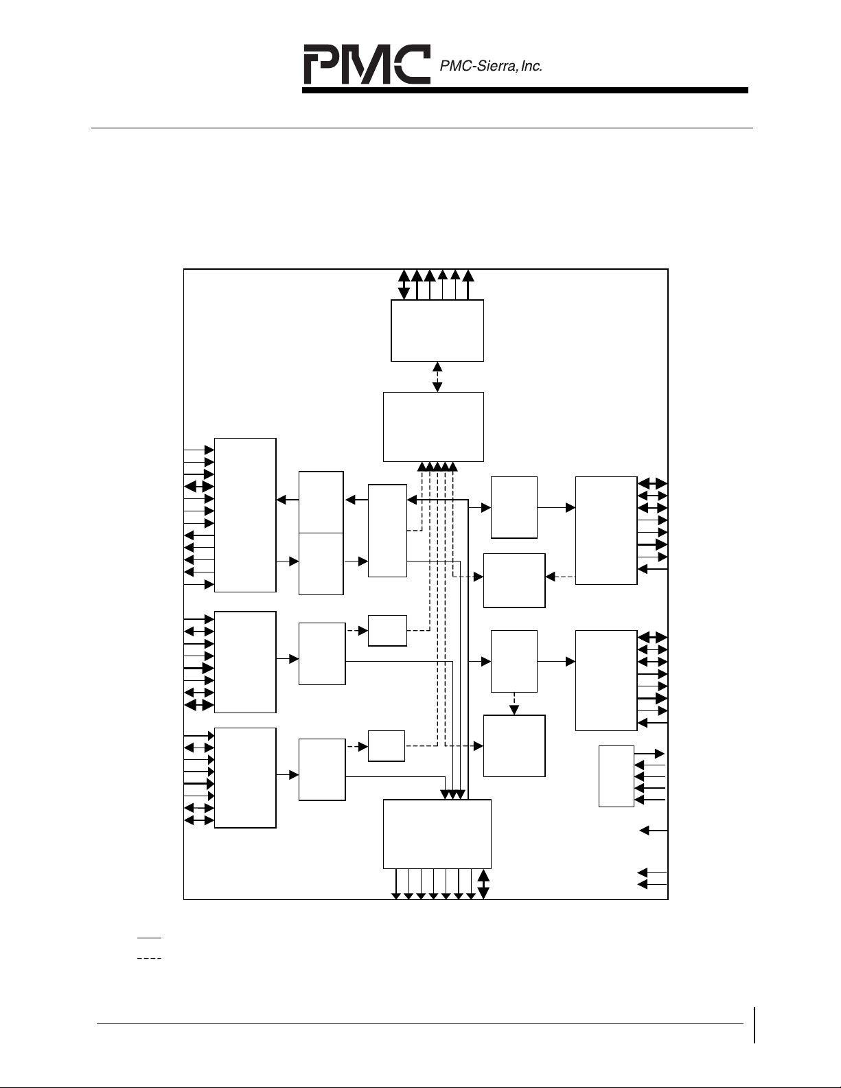
6 BLOCK DIAGRAM
Figure 1 shows the function block diagram of the S/UNI APEX ATM traffic
manager. The functional diagram is arranged such that cell traffic flows through
the S/UNI APEX from left to right.
PROPRIETARY AND CONFIDENTIAL TO PMC-SIERRA, INC., AND FOR ITS CUSTOMERS’ INTERNAL USE 10
Page 27
PM7326 S/UNI APEX
DATA SHEET
PMC-1981224 ISSUE 6 ATM/PACKET TRAFFIC MANAGER AND SWITCH
Figure 1 - S/UNI APEX Block with Datapath
CMD[33:0]
CMP[1:0]
CMA[19:0]
CMRWB
CMCEB
CMAB[18:17]
SSRAM I/F
Queue Engine
BCLK
CSB
WR
AD[31:0]
ADSB
BURSTB
BLAST
READYB
WRDONEB
INTHIB
INTLOB
BUSPOL
uProc I/F
FIFO
4 chan
2 cell
FIFO
2 cell
SAR
Assist
FIFO
4 cell
Loop Port
Scheduler
Loop Tx
Any-PHY
LTADR[11:0]
LTPA
LTENB
LTSX
LTSOP
LTDAT[15:0]
LTPRTY
LTCLK
LRCLK
LRPA
LRSX
LRSOP
LRDAT[15:0]
LRPRTY
LRENB
LRADR[5:0]
WRCLK
WRPA
WRSX
WRSOP
WRDAT[15:0]
WRPRTY
WRENB
WRADDR[2:0]
Loop Rx
Any-PHY
WAN Rx
Any-PHY
Cell Data Path
Context Data Path
FIFO
4 cell
FIFO
4 cell
ICI
Select
ICI
Select
SDRAM I/F
B
B
B
S
S
S
A
A
C
R
B
C
B
B
C
C
C
WTADR[2:0]
FIFO
4 chan
4 cell
Wan
Port
Scheduler
]
]
]
B
E
W
R
B
C
]
0
0
0
0
:
:
:
:
1
1
1
1
[
[
1
3
[
[
S
M
A
B
Q
Q
B
B
D
D
C
C
B
B
C
C
WAN Tx
Any-PHY
JTAG
WTPA
WTENB
WTSX
WTSOP
WTDAT[15:0]
WTPRTY
WTCLK
TDO
TDI
TCK
TMS
TRSTB
SYSCLK
RSTB
OE
PROPRIETARY AND CONFIDENTIAL TO PMC-SIERRA, INC., AND FOR ITS CUSTOMERS’ INTERNAL USE 11
Page 28

PM7326 S/UNI APEX
DATA SHEET
PMC-1981224 ISSUE 6 ATM/PACKET TRAFFIC MANAGER AND SWITCH
7 DESCRIPTION
The PM7326 S/UNI APEX is a full duplex ATM traffic management device,
providing cell switching, per VC queuing, traffic shaping, congestion
management, and hierarchical scheduling to up to 2048 loop ports and up to 4
WAN ports.
The S/UNI APEX provides per-VC queuing for 64K VCs. A per-VC queue may be
allocated to any Class of Service (COS), within any port, in either direction
(ingress or egress path). Per-VC queuing enables PCR or SCR per-VC shaping
on WAN ports and greater fairness of bandwidth allocation between VCs within a
COS.
The S/UNI APEX provides three level hierarchical scheduling for port, COS, and
VC level scheduling. There are two, three level schedulers; one for the loop ports
and one for the WAN ports. The three level scheduler for the WAN ports
provides
• Weighted Interleaved Round Robin (WIRR) scheduling across the 4 WAN
ports enabling selectability of bandwidth allocation between the ports.
• Priority Fair scheduling across the 4 COS’s within each port. This class
scheduler is a modified priority scheduler allowing minimum bandwidth
allocations to lower priority classes within the port. Class scheduling within
a port is independent of activity on all other ports.
• There are three types of VC schedulers. VC scheduling within a class is
independent of activity on all other classes
• Shaped fair queuing is available for 4 classes. If the COS is shaped,
each VC within the class is scheduled for emission based on its VCs
shaping rate. During class congestion, the VC scheduler may lower a
VCs rate in proportion to a normalization factor calculated as a function
of the VCs rate and the aggregate rate of all active VCs within the
class.
• Weighted Interleaved Round Robin scheduling in which weights are
used to provide fairness between the VCs within a class.
• Frame continuous scheduling where an entire packet is accumulated
prior to transferring to a class queue.
The three level scheduler for the loop ports provides
• Weighted Interleaved Round Robin (WIRR) scheduling across the 2048
loop ports enabling selectability of bandwidth allocation between the ports
PROPRIETARY AND CONFIDENTIAL TO PMC-SIERRA, INC., AND FOR ITS CUSTOMERS’ INTERNAL USE 12
Page 29

PM7326 S/UNI APEX
DATA SHEET
PMC-1981224 ISSUE 6 ATM/PACKET TRAFFIC MANAGER AND SWITCH
and ensuring minimal PHY layer FIFOing is required to support a wide
range of port bandwidths.
• Priority scheduling across the 4 COS’s within each port. Class scheduling
within a port is independent of activity on all other ports.
• VCs within a class are scheduled with a Round Robin scheduler or Frame
Continuous scheduling. VC scheduling within a class is independent of
activity on all other classes. Shaping is not supported on loop ports.
The S/UNI APEX forwards cells via tail of queue enqueuing and head of queue
dequeuing (emission) where tail of queue enqueuing is controlled by the VC
context record and subject to congestion control, and head of queue dequeuing
is controlled by the three level hierarchical schedulers. The VC context record
allows for enqueuing to any queue associated with any port, thus full switching is
supported, any port to any port.
The S/UNI APEX supports up to 256k cells of shared buffering in a 32-bit wide
SDRAM. Memory protection is provided via an inband CRC on a cell by cell
basis. Buffering is shared across direction, port, class, and VC levels. The
congestion control mechanism provides guaranteed resources to all active VCs,
allows sharing of available resources to VCs with excess bandwidth, and restricts
buffer allocation on a per-VC, per-class, per-port, and per-direction basis. The
congestion control mechanism supports PPD and EPD on a CLP0 and CLP1
basis across per-VC, per-class, per-port, and per-direction structures. EFCI
marking is supported on a per-VC basis. Congestion thresholds and packet
awareness is selectable on a per connection basis.
The S/UNI APEX provides flexible capabilities for signaling, management, and
control traffic. There are 4 independent uP receive queues to which both cell and
AAL5 frame traffic may be en-queued for termination by the uP. A staging buffer
is also provided enabling the uP to en-queue both cell and AAL5 frame traffic to
any outgoing queue. AAL5 SAR assistance is provided for AAL5 frame traffic to
and from the uP. AAL5 SAR assistance includes the generation and checking of
the 32-bit CRC field and the ability to reassemble all the cells from a frame in the
VC queue prior to placement on the uP queues. Any or all of the 64k VCs may
be configured to be routed to/from the uP port. Any or all of the VCs configured
to be routed to/from the uP port may also be configured for AAL5 SAR
assistance simultaneously. OAM cells may optionally (per-VC selectable) be
routed to a uP receive queue or switched with the user traffic. CRC10 generation
and checking is optionally provided on OAM cells to/from the uP.
The S/UNI APEX maintains cell counts of CLP0 and CLP1 cell transmits on a
per-VC basis. Global CLP0 and CLP1 congestion discards are also maintained.
Various error monitoring conditions and statistics are accumulated or flagged.
PROPRIETARY AND CONFIDENTIAL TO PMC-SIERRA, INC., AND FOR ITS CUSTOMERS’ INTERNAL USE 13
Page 30

PM7326 S/UNI APEX
DATA SHEET
PMC-1981224 ISSUE 6 ATM/PACKET TRAFFIC MANAGER AND SWITCH
The uP has access to both internal S/UNI APEX registers and the context
memory as well as diagnostic access to the cell buffer memory.
The S/UNI APEX provides a 8/16-bit Any-PHY compliant loop side master/slave
interface supporting up to 2048 ports. Egress cell transfers across the interface
are identified via an inband port identifier prepended to the cell. The slave
devices must match the inband port identifier with their own port ID or port ID
range in order to accept the cell. Per port egress flow control is effected via an
12-bit address polling bus to which the appropriate slave device responds with
out of band per port flow control status. Ingress cell transfers across the interface
are effected via a combination of UTOPIA L2 flow control polling and device
selection for up to 32 slave devices. The Any-PHY loop side interface may be
reconfigured as a standard single port UTOPIA L2 compliant slave interface. 16bit prepends are optionally supported on both ingress and egress for cell flow
identification enabling use with external address resolution devices, switch fabric
interfaces, or other layer devices.
The S/UNI APEX provides an 8/16-bit Any-PHY or UTOPIA L2 compliant WAN
side master/slave interface supporting up to 4 ports. 16-bit prepends are
optionally supported on both ingress and egress for cell flow identification
enabling use with external address resolution devices, switch fabric interfaces, or
other layer devices. The WAN port has port aliasing on the egress, providing in
service re-direction without requiring re-programming the context of active VCs.
The S/UNI APEX provides a 32-bit microprocessor bus interface for signaling,
control, cell and frame message extraction and insertion, VC. Class and port
context access, control and status monitoring, and configuration of the IC.
Microprocessor burst access for registers, cell and frame traffic is supported.
The S/UNI APEX provides a 36-bit ZBT or late write SSRAM interface for context
storage supporting up to 4MB of context for up to 64kVCs and up to 256k cell
buffer pointer storage. Context Memory protection is provided via 2 bits of parity
over each 34-bit word.
The total number of cells, the total number of VCs, support for address mapping
and shaped fair queuing is limited to the amount of context and cell buffer
memory available. Below is a table illustrating the most common combinations
of memory/features.
PROPRIETARY AND CONFIDENTIAL TO PMC-SIERRA, INC., AND FOR ITS CUSTOMERS’ INTERNAL USE 14
Page 31

PM7326 S/UNI APEX
DATA SHEET
PMC-1981224 ISSUE 6 ATM/PACKET TRAFFIC MANAGER AND SWITCH
Table 2 - Sample feature set as a function of memory capacity
Context
Memory Size
Cell Buffer
Memory Size
# VC # Cell
Buffers
Address
Mapping
Shaping
Support
Support
SSRAM
SDRAM
1 MB 4MB 16 K 64 K Yes No
2 MB 4MB 16 K 64 K Yes Yes
2 MB 4MB 64 K 64 K No No
4 MB 16MB 64 K 256 K Yes Yes
The S/UNI APEX provides facilities to enable sparing capability with another
S/UNI APEX device. The facilities enable a 'warm standby' capability in which
connection setup between the two devices can be maintained identically but
some cell loss will occur at the point of device swapping. The facilities do not
include a cell by cell lock step between the two S/UNI APEX devices. To avoid
any cell replication, queues in the 'spare' S/UNI APEX will be kept empty, thus
causing all queued traffic in the 'active' S/UNI APEX to be lost at the point of
switch over. However, since connection setup is maintained identically between
the two S/UNI APEX devices, switch over can happen instantaneously, thus
avoiding any connection timeout or tear down issues.
The S/UNI APEX facilities provided are the disable and filter control bits in the
Receive and Transmit Control register. These control bits are asserted in the
spare S/UNI APEX to ensure the queues remain empty until swapping is
initiated. Alternatively, asserting only the filter enable bits allow signalling and
control traffic continuity to be maintained to the spare S/UNI APEX to enable
datapath integrity testing on the spare plane and to ensure control
communications paths to the spare plane are usable.
PROPRIETARY AND CONFIDENTIAL TO PMC-SIERRA, INC., AND FOR ITS CUSTOMERS’ INTERNAL USE 15
Page 32

PM7326 S/UNI APEX
DATA SHEET
PMC-1981224 ISSUE 6 ATM/PACKET TRAFFIC MANAGER AND SWITCH
8 PIN DIAGRAM
The S/UNI APEX is packaged in a 352-pin ball grid array (SBGA) package
having a body size of 35 mm by 35 mm.
Figure 2 - S/UNI APEX Bottom View Pin out
2625242322212019181716151413121110987654321
A
vss5 vss4 CMD [0] CMD [4] CM D [7] CMD [11] CMD [14] CMD [18] CMD [21] PCH CMD [27] CMD [30] vss3 vss2 AD [2] AD [4] PCH AD [10] AD [13] AD [17] AD [20] AD [24] AD [27] AD [31] vss1 vss0
B
vss9 vdd10 vss8 CMD [1] CMD [5] CMD [8] CMD [12] C MD [15] CMD [19] CMD [23] CMD [25] CMD [29] CMD [32] CMD [33] SYSCLK AD [6] AD [8] AD [12] AD [16] AD [19] AD [23] AD [26] AD [30] vss7 vd d9 vss6
C
CMRWB vss11 vdd12 CMP [1] CMD [2] CMD [6] CMD [9] CMD [13] CMD [16] CMD [20] CMD [24] CMD [28] CMD [31] AD [0] AD [3] AD [7] AD [11] AD [15] AD [18] AD [22] AD [25] AD [29] INTHIB vdd11 vss10 BCLK
D
CMAB [1] CMCEB CMP [0] vd d17 nc CMD [3] PCH CMD [10] vdd16 CMD [17] CM D [22] C MD [26] vdd 15 AD [1] AD [5] AD [9] AD [14] vdd14 AD [21] PCH AD [28] nc vdd13 INTLOB W RDONEB BLAST
E
CMA [16] CMA [17] CMA [19] nc BUSPOL BTERMB BURSTB C SB
F
CMA [12] CMA [15] CMAB [0] CMA [18] READYB WR ADSB LRADR [2]
G
CMA [9] CMA [11] CMA [14] PCH PCH LRA DR [0] LRADR [3] LRADR [5]
H
CMA [5] CMA [8] CMA [10] CMA [13] LRADR [1] LRADR [4] LRENB LRPRTY
J
CMA [2] CMA [4] CMA [7] vdd18 vd d 1 9 L RPA LRSO P LRDA T [0 ]
K
PCH CMA [0] CMA [3] CMA [6] LRC LK LRSX LRDA T [ 1] LRDA T [3 ]
L
LTDAT [12] LTDAT [14] LTDAT [15] CMA [1] PCH LRDAT [2] LRDAT [4] LRDAT [6]
M
LTD A T [ 9] L TDA T [ 1 0 ] LTDA T [ 1 1 ] LTD AT [ 1 3 ] LRDAT [5] LRDAT [7] LRDAT [8] LRDAT [9]
N
v ss1 3 LTD A T [ 6 ] LTDA T [ 7 ] LTDA T [ 8 ] vd d20 LRDAT [10] LRDAT [11] vss12
P
v ss1 5 LTD A T [ 5 ] LTDA T [ 4 ] v d d 2 1 LRDAT [14] LRDAT [13] LRDAT [12] vss14
WRADR
R
LTD A T [ 3] LTD A T [ 2 ] L TDA T [ 1 ] L TPA PCH
T
LTDAT [ 0] LTCLK LTENB LTSOP WRSOP WRCLK WRENB
U
PCH LTSX LTADR [11] LTADR [8] WRDAT [3] WRDAT [0] WRPRTY WRPA
V
LTPRTY LTAD R [10 ] LTA DR [7 ] v d d2 3 vdd22 WRDAT [4] WRDAT [1] WRSX
W
LTADR [9] LTADR [6] LTADR [4] LTADR [1] PC H WRDAT [7] WRDA T [5] WRDA T [2]
Y
LTADR [5] LTADR [3] LTADR [0]
WTDAT
AA
LTADR [ 2]
[15]
WTDAT
AB
PCH
[12]
WTDAT
AC
WTDAT [8] WTDAT [6] vdd4 SCANMB WTDAT [2] WTENB WTSOP vd d3 CBA [9] C BA [4] CBA [0] CBCASB vdd 2
[11]
AD
WTDA T [7] v ss17 vd d 6 SC AN EN W TDAT [ 3] WTPA W TCLK WTADR [ 1] C BA [1 0] C BA [6 ] CBA [ 2] CBBS [0 ] CBWEB
AE
vss21 vdd8 vss19 WTDAT [4] WTDAT [0] WTSX WTADR [0] CBA [11] CBA [7] CBA [3] CBA [1] CBCSB
AF
vss27 v ss26 WTDA T [5] WTDA T [1 ] PC H WTPRTY WTAD R [2] CBA [8 ] CBA [ 5] PC H C BBS [1 ] C BRASB vss25 v ss24
2625242322212019181716151413121110987654321
WTDAT
[14]
WTDAT
WTDAT
[13]
[10]
WTDAT [9] nc nc TDI
vdd1
CBDQ
[16]
CBDQ
[19]
CBDQ
[21]
CBDQ
CBDQ [7] C BDQ [3] nc vdd 0 TRSTB TMS OE
[10]
CBDQ
CBDQ [9] C BDQ [6] CBDQ [2] TDO vdd5 vss16 TCK
[13]
CBDQ
CBDQ
CBDQ [8] CBDQ [5] CBDQ [1] vss20 vdd7 vss18
[15]
[12]
CBDQ
CBDQ
[18]
CBDQ
[14]
[11]
CBDQ M
[1]
CBDQ
[31]
CBDQM
[0]
CBDQ
[26]
CBDQ
[28]
CBDQ
[29]
CBDQ
[30]
CBDQ
[22]
CBDQ
[24]
CBDQ
[25]
CBDQ
[27]
CBDQ
[17]
CBDQ
[20]
CBDQ
[23]
PCH
WRDAT
[13]
RSTB
PCH C BDQ [ 4] CBD Q [0 ] v ss23 vss22
[1]
WRDAT
[10]
WRDAT
[14]
WRADR
WRDAT [8]WRDAT [6]
WRDAT
WRDAT
[0]
[11]
[15]
LRDA T [ 15 ]
WRADR
[2]
WRDAT [9]
WRDAT
[12]
A
B
C
D
E
F
G
H
J
K
L
M
N
P
R
T
U
V
W
Y
AA
AB
AC
AD
AE
AF
PROPRIETARY AND CONFIDENTIAL TO PMC-SIERRA, INC., AND FOR ITS CUSTOMERS’ INTERNAL USE 16
Page 33

PM7326 S/UNI APEX
DATA SHEET
PMC-1981224 ISSUE 6 ATM/PACKET TRAFFIC MANAGER AND SWITCH
9 PIN DESCRIPTION
Notes on Pin Description:
1. All S/UNI APEX inputs and bi-directionals present minimum capacitative
loading
2. LVCMOS, LVTTL compatible logic levels.
3. All pins are 5V tolerant.
4. Inputs RSTB, OE, TMS, TDI and TRSTB have internal pull-up resistors.
5. The recommended power supply sequencing is as follows:
3.1VDD power must be supplied either before or simultaneously with PCH.
3.2The VDD power must be applied before input pins are driven or the input
current per pin be limited to less than the maximum DC input current
specification. (20 mA)
3.3Power down the device in the reverse sequence.
Table 3 - Pin Type Definition
Type Definition
Input Input
Output Pin is always driven
Tri-State Pin is either driven, or held in Hi-Z
BiDi Bidirectional
OD Open drain. Either driven low or held in Hi-Z.
9.1 Loop Any-PHY Receive Master/Transmit Slave Interface (28 Signals)
Pin Name Type Pin
Function
No.
LRCLK Input
K4
Loop Receive Clock. LRCLK is used to transfer
data blocks in the receive directions across the AnyPHY interface. LRCLK must cycle at a 52 MHz or
lower instantaneous rate.
PROPRIETARY AND CONFIDENTIAL TO PMC-SIERRA, INC., AND FOR ITS CUSTOMERS’ INTERNAL USE 17
Page 34

PM7326 S/UNI APEX
DATA SHEET
PMC-1981224 ISSUE 6 ATM/PACKET TRAFFIC MANAGER AND SWITCH
Pin Name Type Pin
No.
LRPA Input
J3
(Master)
Tri-state
(Slave)
Function
Loop Receive Packet Available. LRPA indicates
whether at least one cell is queued for transfer in
the selected PHY device.
This pin is in Hi-Z when the loop receive interface is
not enabled.
If receive master mode is selected, this signal is an
input. The selected PHY device drives LRPA with
the cell availability status N LRCLK cycles after
LRADR[5:0] matches the PHY device address. If the
PHY device is a UTOPIA device, N=1. If the PHY
device is an Any-PHY device, N=2. Assertion of
LRPA indicates that at least one entire cell is
available.
If transmit slave mode is selected, this signal is a tristate output. The S/UNI APEX drives LRPA high 1
LRCLK after LRADR[5:0] matches the programmed
LoopRxSlaveAddr register. A logical high indicates
that the S/UNI APEX is capable of accepting at least
one cell.
LRPA is sampled/updated/Hi-Z’d on the rising edge
of LRCLK.
PROPRIETARY AND CONFIDENTIAL TO PMC-SIERRA, INC., AND FOR ITS CUSTOMERS’ INTERNAL USE 18
Page 35

PM7326 S/UNI APEX
DATA SHEET
PMC-1981224 ISSUE 6 ATM/PACKET TRAFFIC MANAGER AND SWITCH
Pin Name Type Pin
No.
LRENB Input
H2
(Slave)
Output
(Master)
Function
Loop Receive Enable. The active low receive
enable (LRENB) signal is used to initiate the
transfer of a data block from the selected Physical
layer device to the S/UNI APEX.
This pin is in Hi-Z when the loop receive interface is
not enabled.
If receive master mode is selected, this signal is an
output and the start of block transfer must occur 1
or 2 LRCLK cycles after device selection occurs. If
the PHY device is a UTOPIA device, N=1. If the
PHY device is an Any-PHY device, N=2. Device
selection occurs when the selected device address
is placed on LRADR[5:0] with LRENB held high
followed by LRENB low in the next LRCLK period.
LRENB is held low for M cycles where M is the
number of 8 or 16-bit words in the block transfer.
If transmit slave mode is selected, this signal is an
input and LRDAT[15:0] word is accepted coincident
with LRENB being sampled.
LRENB is sampled/updated on the rising edge of
LRCLK.
PROPRIETARY AND CONFIDENTIAL TO PMC-SIERRA, INC., AND FOR ITS CUSTOMERS’ INTERNAL USE 19
Page 36

PM7326 S/UNI APEX
DATA SHEET
PMC-1981224 ISSUE 6 ATM/PACKET TRAFFIC MANAGER AND SWITCH
Pin Name Type Pin
No.
LRADR[0]
..
LRADR[5]
Input
(Slave)
Output
(Master)
G3
H4
F1
G2
H3
G1
Function
Loop Receive Address. The LRADR[5:0] signals
are used to address up to thirty two Physical layer
devices for the purposes of polling and device
selection.
This pin is in Hi-Z when the loop receive interface is
not enabled.
If UL2 or Any-PHY receive master mode is selected,
these signals are outputs. LRADR[5:0] selects a
device for polling by applying the device address N
LRCLK cycles prior to sampling LRPA. If the PHY
device is a UTOPIA device, N=1. If the PHY device
is an Any-PHY device, N=2. LRADR will insert 1
NULL address between address changes.
If UL1 master mode is selected, this bus is driven to
a high NULL address.
LRADR[5:0] selects a device to transfer a data block
when the LRENB is last sampled high. The start of
data block transfer must occur 1 or 2 LRCLK cycles
after device selection occurs.
LRSX Input
K3
LRADR[5:0] = 3F hex is used as the NULL address.
No PHY device can match the NULL address.
If transmit slave mode is selected, these signals are
inputs. The S/UNI drives the LRPA 1 LRCLK after
the LRADR[4:0] matches the programmed
LoopRxSlaveAddr register, and LRADR[5] is zero.
LRADR[5:0] is sampled/updated or on the rising
edge of LRCLK.
Loop Receive Start of Transfer. LRSX is asserted
by the selected PHY device during the first cycle of
a data block transfer coinciding with the port
address prepend. Required only during Any-PHY
mode.
For UTOPIA modes, this signal should be tied low.
LRSX is sampled on the rising edge of LRCLK.
PROPRIETARY AND CONFIDENTIAL TO PMC-SIERRA, INC., AND FOR ITS CUSTOMERS’ INTERNAL USE 20
Page 37

PM7326 S/UNI APEX
DATA SHEET
PMC-1981224 ISSUE 6 ATM/PACKET TRAFFIC MANAGER AND SWITCH
Pin Name Type Pin
No.
LRSOP Input
LRDAT[0]
Input
..
LRDAT[15]
J2
J1
K2
L3
K1
L2
M4
L1
M3
M2
M1
N3
N2
P2
P3
P4
R1
Function
Loop Receive Start of Packet . LRSOP marks the
start of the cell on the LRDAT[15:0] bus. When
LRSOP is high, the first data word of the cell is
present on the LRDAT[15:0] stream. If the selected
device is an Any-PHY device, the LRSOP cycle will
be preceded by the LRSX cycle marking the AnyPHY port address transfer cycle.
LRSOP considered valid only when the LRENB
signal is low. LRSOP becomes high impedance
upon sampling LRENB high or if no physical layer
device was selected for transfer.
LRSOP is sampled on the rising edge of LRCLK.
Loop Receive Data. LRDAT[15:0] carries the
transfer block words that have been read from the
physical layer device to the S/UNI APEX internal cell
buffers.
LRDAT bus is considered valid only when the
LRENB signal was low N cycles previous. LRDAT is
expected to become high impedance N LRCLK
cycles after sampling LRENB high or upon
completion of a data block transfer. If the PHY
device is a UTOPIA device, N=1. If the PHY device
is an Any-PHY device, N=2.
All 16 bits are used in 16-bit mode. In 8 bit mode,
LRDAT[15:8] should either be tied high or low, as
only the first 8 bits LTDAT[7:0] are valid.
LRDAT[15:0] is sampled on the rising edge of
LRCLK.
PROPRIETARY AND CONFIDENTIAL TO PMC-SIERRA, INC., AND FOR ITS CUSTOMERS’ INTERNAL USE 21
Page 38

PM7326 S/UNI APEX
DATA SHEET
PMC-1981224 ISSUE 6 ATM/PACKET TRAFFIC MANAGER AND SWITCH
Pin Name Type Pin
Function
No.
LRPRTY Input
H1
Loop Receive Parity. LRPRTY provides
programmable odd/even parity of the LRDAT[15:0]
bus.
LRPRTY is considered valid only when the LRENB
signal was low N cycles previous. If the PHY device
is a UTOPIA device, N=1. If the PHY device is an
Any-PHY device, N=2. LRPRTY is expected to
become high impedance N LRCLK cycles after
sampling LRENB high.
A parity error is indicated by a status bit and a
maskable interrupt.
LRPRTY is sampled on the rising edge of LRCLK.
9.2 Loop Any-PHY Transmit Master/Receive Slave Interface (34 Signals)
Pin Name Type Pin
Function
No.
LTCLK Input T25
Loop Transmit Clock. LTCLK is used to transfer
data blocks in the transmit direction across the AnyPHY interface. LTCLK must cycle at a 52 MHz or
lower instantaneous rate.
PROPRIETARY AND CONFIDENTIAL TO PMC-SIERRA, INC., AND FOR ITS CUSTOMERS’ INTERNAL USE 22
Page 39

PM7326 S/UNI APEX
DATA SHEET
PMC-1981224 ISSUE 6 ATM/PACKET TRAFFIC MANAGER AND SWITCH
Pin Name Type Pin
No.
LTADR[0]
..
LTADR[11 ]
Output
(Master)
Input
(Slave)
Y24
W23
AA26
Y25
W24
Y26
W25
V24
U23
W26
V25
U24
Function
Loop Transmit Address. The LTADR[11:0] signals
are used to address up to 2048 logical channels for
the purposes of polling on the LTPA signal. 1 or
more PHY devices can share the LTPA signal
This pin is in Hi-Z when the loop transmit interface is
not enabled.
If transmit master mode is selected, these signals
are outputs. LTADR[11:0] selects a logical channel
for polling by applying the logical channel address N
LTCLK cycles prior to sampling LTPA. If the PHY
device is a UTOPIA device, N=1. If the PHY device
is an Any-PHY device, N=2. LTADR inserts NULL
cycles between addresses.
For Any-PHY transmit master, LTADR[11:0]
corresponds to the PORTID[11:0] fields in the AnyPHY address word prepend format.
For UTOPIA L2 transmit master, LTADR[5:0] is also
used to select a UTOPIA device to transfer a cell to,
when LTENB is last sampled high. LTADR[11:6]
should be left unconnected.
For UTOPIA L1 transmit master, LTADR[11:0] is
unused and should be left unconnected.
If UTOPIA L2 receive slave mode is selected, these
signals are inputs. The S/UNI APEX drives LTPA
high 1 LTCLK after the LTADR[5:0] matches the
programmed LoopTxSlaveAddr register.
LTADR[11:6] are unused and should be tied either
high or low.
LTADR[11:0] is sampled/updated on the rising edge
of LTCLK.
PROPRIETARY AND CONFIDENTIAL TO PMC-SIERRA, INC., AND FOR ITS CUSTOMERS’ INTERNAL USE 23
Page 40

PM7326 S/UNI APEX
DATA SHEET
PMC-1981224 ISSUE 6 ATM/PACKET TRAFFIC MANAGER AND SWITCH
Pin Name Type Pin
No.
LTPA Input
R23
(Master)
Tri-state
(Slave)
Function
Loop Transmit Packet Available. LTPA indicates
the availability of space in the selected polled port
when polled using the LTADR[11:0] signals.
This pin is in Hi-Z when the loop transmit interface is
not enabled.
If transmit master mode is selected, this signal is an
input. The PHY device whose address or address
range matches LTADR[11:0] drives the LTPA signal
with the transmit FIFO availability status of the
selected logical channel N LTCLK cycles after the
match. If the PHY device is a UTOPIA device, N=1.
If the PHY device is an Any-PHY device, N=2.
Assertion of LTPA indicates that at least K entire cell
buffer is available in that logical channel. K = 1 if
the register LoopTxTwoCellEn = 0. K = 2 if the
register LoopTxTwoCellEn = 1.
If receive slave mode is selected, this signal is a tristate output. The S/UNI APEX drives LTPA 1
LTCLK after LTADR[5:0] matches the programmed
LoopTxSlaveAddr register. A logical high indicates
that at least one cell is available for transmission.
LTPA is sampled/updated/Hi-Z’d on the rising edge
of LTCLK.
LTENB Output
(Master)
T24
Loop Transmit Enable. LTENB indicates cell
transfers to UTOPIA and SCI-PHY devices. The
device is selected via a match on LTADR[11:0] when
Input
(Slave)
LTENB is last sampled high.
This pin is in Hi-Z when the loop transmit interface is
not enabled.
If transmit master mode is selected, this signal is an
output. LTENB is held low for the duration of the cell
transfer.
If receive slave mode is selected, this signal is an
input.
LTENB is sampled/updated on the rising edge of
LTCLK.
PROPRIETARY AND CONFIDENTIAL TO PMC-SIERRA, INC., AND FOR ITS CUSTOMERS’ INTERNAL USE 24
Page 41

PM7326 S/UNI APEX
DATA SHEET
PMC-1981224 ISSUE 6 ATM/PACKET TRAFFIC MANAGER AND SWITCH
Pin Name Type Pin
No.
LTSX Output U25
LTSOP Output
T23
(Master)
Tri-state
(Slave)
Function
Loop Transmit Start of Transfer. LTSX is asserted
by the S/UNI APEX during the first cycle of a data
block transfer. LTSX assertion will coincide with the
port address prepend, if the cell being transferred
has a prepended port address. Required only
during Any-PHY mode. Should be left unconnected
during UTOPIA modes.
LTSX is updated on the rising edge of LTCLK.
Loop Transmit Start of Cell. LTSOP marks the
start of cell on the LTDAT[15:0] data bus. LTSOP is
driven high when the first word of the cell (excluding
address prepend) is present on the LTDAT[15:0]
stream. LTSOP is asserted for each cell.
In transmit master mode, the signal is always
driven.
In receive slave mode, this signal is driven 1 LTCLK
after LTENB is asserted.
LTDAT[0]
..
LTDAT[15]
Output
(Master)
Tri-state
(Slave)
T26
R24
R25
R26
P24
P25
N25
N24
N23
M26
M25
M24
L26
M23
L25
L24
LTSOP is updated/Hi-Z’d on the rising edge of
LTCLK.
Loop Transmit Data. LTDAT[15:0] carries the data
block transfers to the physical layer devices.
In 8 bit mode, only LTDAT[7:0] are valid.
In transmit master mode, the entire bus is always
driven.
In receive slave mode, this bus is driven 1 LTCLK
after LTENB is asserted. Pull up/downs are
required for the entire bus, regardless of whether
the bus is in 8 or 16 bit mode.
LTDAT[15:0] is updated/Hi-Z’d on the rising edge of
LTCLK.
PROPRIETARY AND CONFIDENTIAL TO PMC-SIERRA, INC., AND FOR ITS CUSTOMERS’ INTERNAL USE 25
Page 42

PM7326 S/UNI APEX
DATA SHEET
PMC-1981224 ISSUE 6 ATM/PACKET TRAFFIC MANAGER AND SWITCH
Pin Name Type Pin
Function
No.
LTPRTY Output
(Master)
V26
Loop Transmit Parity. This signal provides
programmable odd/even parity of the LTDAT[15:0]
bus.
Tri-state
(Slave)
In transmit master mode, the signal is always
driven.
In receive slave mode, this signal is driven 1 LTCLK
after LTENB is asserted.
LTPRTY is updated/Hi-Z’d on the rising edge of
LTCLK.
9.3 WAN Any-PHY Receive Master/Transmit Slave Interface (25 Signals)
Pin Name Type Pin
Function
No.
WRCLK Input T3
WAN Receive Clock. WRCLK is used to transfer
data blocks in the receive direction across the AnyPHY interface. WRCLK must cycle at a 52 MHz or
lower instantaneous rate.
PROPRIETARY AND CONFIDENTIAL TO PMC-SIERRA, INC., AND FOR ITS CUSTOMERS’ INTERNAL USE 26
Page 43

PM7326 S/UNI APEX
DATA SHEET
PMC-1981224 ISSUE 6 ATM/PACKET TRAFFIC MANAGER AND SWITCH
Pin Name Type Pin
No.
WRPA Input
U1
(Master)
Tri-state
(Slave)
Function
WAN Receive Packet Available. WRPA indicates
cell availability.
This pin is in Hi-Z when the WAN receive interface
is not enabled.
If master mode is selected, the selected PHY device
drives WRPA with the cell availability status N
WRCLK cycles after WRADR[2:0] matches the PHY
device address. If the PHY device is a UTOPIA
device, N=1. If the PHY device is an Any-PHY
device, N=2. Assertion of WRPA indicates that at
least one entire cell is available.
If slave mode is selected, this signal is an output
and the S/UNI APEX plays the roll of a single port
UTOPIA L2 slave device driving the WRPA when the
WRADR matches the programmed
WANRxSlaveAddr register. A logical high indicates
that the S/UNI APEX is capable of accepting at least
one cell.
WRPA is sampled/updated/Hi-Z’d on the rising edge
of WRCLK.
PROPRIETARY AND CONFIDENTIAL TO PMC-SIERRA, INC., AND FOR ITS CUSTOMERS’ INTERNAL USE 27
Page 44

PM7326 S/UNI APEX
DATA SHEET
PMC-1981224 ISSUE 6 ATM/PACKET TRAFFIC MANAGER AND SWITCH
Pin Name Type Pin
No.
WRENB Output
T2
(Master)
Input
(Slave)
Function
WAN Receive Enable. The active low receive
enable (WRENB) output is used to initiate the
transfer of a data block from the selected Physical
layer device to the S/UNI APEX.
This pin is in Hi-Z when the WAN receive interface
is not enabled.
If master mode is selected, this signal is an output
and the start of block transfer must occur 1 or 2
WRCLK cycles after device selection occurs. Device
selection occurs when the selected device address
is placed on WRADR[2:0] with WRENB held high
followed by WRENB low in the next WRCLK period.
WRENB is held low for M cycles where M is the
number of 8 or 16-bit words in the block transfer.
If slave mode is selected, this signal is an input and
WRDAT[15:0] word is accepted coincident with
WRENB being sampled.
WRENB is sampled/updated on the rising edge of
WRCLK.
PROPRIETARY AND CONFIDENTIAL TO PMC-SIERRA, INC., AND FOR ITS CUSTOMERS’ INTERNAL USE 28
Page 45

PM7326 S/UNI APEX
DATA SHEET
PMC-1981224 ISSUE 6 ATM/PACKET TRAFFIC MANAGER AND SWITCH
Pin Name Type Pin
No.
WRADR[0]
..
WRADR[2]
Output
(Master)
R2
R3
T1
Input
(Slave)
Function
WAN Receive Address. The WRADR[2:0] signals
are used to address up to four Physical layer
devices for the purposes of polling and device
selection.
This pin is in Hi-Z when the WAN receive interface
is not enabled.
If UL2 or Any-PHY receive master mode is selected,
this bus is an output. WRADR[2:0] selects a device
for polling by applying the device address N
WRCLK cycles prior to sampling WRPA. If the PHY
device selected is a UTOPIA device, N=1. If the
PHY device selected is an Any-PHY device, N=2.
When supporting multiple PHYs, WRADR will insert
1 NULL address between address changes.
If UL1 master mode is selected, this bus is driven to
a high NULL address.
WRADR[2:0] selects a device to transfer a data
block when the WRENB is last sampled high. The
start of data block transfer must occur 1 or 2
WRCLK cycles after device selection occurs.
WRSX Input V1
WRADR[2:0] = 7 hex is used as the NULL address.
No PHY device can match the NULL address.
If slave mode is selected, this signal is an input and
the S/UNI APEX plays the roll of a single port
UTOPIA L2 slave device driving the WRPA 1
WRCLK after the WRADR[1:0] matches the
programmed WANRxSlaveAddr register, and
WRADR[2] is zero.
WRADR[2:0] is sampled/updated on the rising edge
of WRCLK.
WAN Receive Start of Transfer. WRSX is asserted
by the selected PHY device during the first cycle of
a data block transfer coinciding with the port
address prepend. WRSX is ignored during cell
transfers from UTOPIA or SCI-PHY devices.
WRSX is updated on the rising edge of WRCLK.
PROPRIETARY AND CONFIDENTIAL TO PMC-SIERRA, INC., AND FOR ITS CUSTOMERS’ INTERNAL USE 29
Page 46

PM7326 S/UNI APEX
DATA SHEET
PMC-1981224 ISSUE 6 ATM/PACKET TRAFFIC MANAGER AND SWITCH
Pin Name Type Pin
No.
WRSOP Input T4
WRDAT[0]
..
WRDAT[15]
Input U3
V2
W1
U4
V3
W2
Y1
W3
Y2
AA1
Y3
AA2
AB1
Y4
AA3
AB2
Function
WAN Receive Start of Packet . WRSOP marks the
start of the cell on the WRDAT[15:0] bus. When
WRSOP is high, the first data word of the cell is
present on the WRDAT[15:0] stream. If the selected
device is an Any-PHY device, the WRSOP cycle will
be preceeded by the WRSX cycle marking the AnyPHY port address transfer cycle.
WRSOP is considered valid only when the WRENB
signal is low. WRSOP becomes high impedance
upon sampling WRENB high or if no physical layer
device was selected for transfer.
WRSOP is sampled on the rising edge of WRCLK.
WAN Receive Data. WRDAT[15:0] carries the
transfer block words that have been read from the
physical layer device to the S/UNI APEX internal cell
buffers. All 16 bits are used in 16-bit mode, only the
first 8 bits WRDAT[7:0] are valid in 8-bit mode.
The WRDAT bus is considered valid only when the
WRENB signal was low N cycles previous. WRDAT
is expected to become high impedance N WRCLK
cycles after sampling WRENB high or upon
completion of a data block transfer. If the PHY
device selected is a UTOPIA device, N=1. If the
PHY device selected is an Any-PHY device, N=2.
WRDAT[15:0] is sampled on the rising edge of
WRCLK.
PROPRIETARY AND CONFIDENTIAL TO PMC-SIERRA, INC., AND FOR ITS CUSTOMERS’ INTERNAL USE 30
Page 47

PM7326 S/UNI APEX
DATA SHEET
PMC-1981224 ISSUE 6 ATM/PACKET TRAFFIC MANAGER AND SWITCH
Pin Name Type Pin
Function
No.
WRPRTY Input U2
WAN Receive Parity. WRPRTY provides
programmable odd/even parity of the WRDAT[15:0]
bus.
The WRPRTY signal is considered valid only when
the WRENB signal was low N cycles previous. If the
PHY device selected is a UTOPIA device, N=1. If
the PHY device selected is an Any-PHY device,
N=2. WRPRTY is expected to become high
impedance N WRCLK cycles after sampling
WRENB high.
A parity error is indicated by a status bit and a
maskable interrupt.
WRPRTY is sampled on the rising edge of WRCLK.
9.4 WAN Any-PHY Transmit Master/Receive Slave Interface (25 Signals)
Pin Name Type Pin
Function
No.
WTCLK Input
AD20
WAN Transmit Clock. WTCLK is used to transfer
data blocks in the transmit direction across the AnyPHY interface. WTCLK must cycle at a 52 MHz or
lower instantaneous rate.
PROPRIETARY AND CONFIDENTIAL TO PMC-SIERRA, INC., AND FOR ITS CUSTOMERS’ INTERNAL USE 31
Page 48

PM7326 S/UNI APEX
DATA SHEET
PMC-1981224 ISSUE 6 ATM/PACKET TRAFFIC MANAGER AND SWITCH
Pin Name Type Pin
No.
WTADR[0]
..
WTADR[2]
Output
(Master)
AE20
AD19
AF20
Input
(Slave)
Function
WAN Transmit Address. The WTADR[2:0] signals
are used to address up to four logical channels for
the purposes of polling.
This pin is in Hi-Z when the WAN transmit interface
is not enabled.
If master mode is selected, these signals are
outputs. WTADR[2:0] selects a logical channel for
polling by applying the logical channel address N
WTCLK cycles prior to sampling WTPA. If the PHY
devices are UTOPIA devices, N=1. If the PHY
devices are Any-PHY devices, N=2. , WTADR will
insert 1 NULL address between address changes
For Any-PHY transmit master, WTADR[1:0]
corresponds to the PORTID[1:0] fields in the AnyPHY address word prepend format.
WTADR[2:0] = 7 hex is used as the NULL address.
No PHY device can match the NULL address.
For UTOPIA L2 transmit master, WTADR[2:0]
signals are also used for cell transfer PHY selection
to UTOPIA compliant PHY devices. WTADR[2:0]
selects a device to transfer a data block to when the
WRENB is last sampled high.
For UTOPIA L1 transmit master, WTADR[1:0]
contains the value of the WANTxSlaveAddr register.
WTADR[2] is held low.
If UTOPIA L2 receive slave mode is selected, these
signals are inputs and the S/UNI APEX plays the roll
of a single port UTOPIA L2 slave device driving the
WTPA 1 WTCLK after the WTADR matches the
programmed WANTxSlaveAddr register.
WTADR[2:0] is sampled/updated on the rising edge
of WTCLK.
PROPRIETARY AND CONFIDENTIAL TO PMC-SIERRA, INC., AND FOR ITS CUSTOMERS’ INTERNAL USE 32
Page 49

PM7326 S/UNI APEX
DATA SHEET
PMC-1981224 ISSUE 6 ATM/PACKET TRAFFIC MANAGER AND SWITCH
Pin Name Type Pin
No.
WTPA Input
AD21
(Master)
Tri-state
(Slave)
Function
WAN Transmit Packet Available. WTPA indicates
cell availability.
This pin is in Hi-Z when the WAN transmit interface
is not enabled.
If master mode is selected, this signal is an input.
The PHY device whose address or address range
matches WTADR[2:0] drives the WTPA signal with
the transmit FIFO availability status of the selected
logical channel N WTCLK cycles after the match. If
the PHY devices are UTOPIA devices, N=1. If the
PHY devices are Any-PHY devices, N=2. Assertion
of WTPA indicates that at least one entire cell buffer
is available in that logical channel.
If slave mode is selected, this signal is a tri-state
output and the S/UNI APEX plays the roll of a single
port UTOPIA L2 slave device driving the WTPA
when the WTADR matches the programmed
WANTxSlaveAddr register. A logical high indicates
that at least one cell is available for transmission.
WTENB Output
(Master)
Input
(Slave)
AC20
WTPA is sampled/updated/Hi-Z’d on the rising edge
of WTCLK.
WAN Transmit Enable. WTENB indicates cell
transfers to UTOPIA and SCI-PHY devices. The
device is selected via a match on WTADR[2:0] when
WTENB is last sampled high.
This pin is in Hi-Z when the WAN transmit interface
is not enabled.
If master mode is selected, this signal is an output.
If slave mode is selected, this signal is an input.
WTENB is held low for the duration of the cell
transfer.
WTENB is sampled/updated on the rising edge of
WTCLK.
PROPRIETARY AND CONFIDENTIAL TO PMC-SIERRA, INC., AND FOR ITS CUSTOMERS’ INTERNAL USE 33
Page 50

PM7326 S/UNI APEX
DATA SHEET
PMC-1981224 ISSUE 6 ATM/PACKET TRAFFIC MANAGER AND SWITCH
Pin Name Type Pin
No.
WTSX Output
WTSOP Output
AE21
AC19
(Master)
Tri-state
(Slave)
Function
WAN Transmit Start of Transfer. WTSX is asserted
by the S/UNI APEX during the first cycle of a data
block transfer. WTSX assertion will coincide with the
port address prepend, if the cell being transferred
has a prepended port address. Required only during
Any-PHY mode.
WTSX is updated on the rising edge of WTCLK.
WAN Transmit Start of Packet. WTSOP marks the
start of cell on the WTDAT[15:0] data bus. WTSOP
is driven high when the first word of the cell
(excluding address prepend) is present on the
WTDAT[15:0] stream. WTSOP is asserted for each
cell.
In transmit master mode, the signal is always
driven.
In receive slave mode, this signal is driven 1
WTCLK after WTENB is asserted.
WTDAT[0]
..
WTDAT[15]
Output
(Master)
Tri-state
(Slave)
AE22
AF23
AC21
AD22
AE23
AF24
AC24
AD26
AC25
AB24
AA23
AC26
AB25
AA24
Y23
AA25
WTSOP is updated/Hi-Z’d on the rising edge of
WTCLK.
WAN Transmit Data. WTDAT[15:0] carries the data
block transfers to the physical layer devices.
In 8 bit mode, only WTDAT[7:0] are valid.
In 8/16bit transmit master mode, the entire bus is
always driven.
In receive slave mode, this bus is driven 1 WTCLK
after WTENB is asserted Pull up/downs are
required for the entire bus, regardless of whether
the bus is in 8 or 16 bit mode.
WTDAT[15:0] is updated/Hi-Z’d on the rising edge
of WTCLK.
PROPRIETARY AND CONFIDENTIAL TO PMC-SIERRA, INC., AND FOR ITS CUSTOMERS’ INTERNAL USE 34
Page 51

PM7326 S/UNI APEX
DATA SHEET
PMC-1981224 ISSUE 6 ATM/PACKET TRAFFIC MANAGER AND SWITCH
Pin Name Type Pin
No.
WTPRTY Output
AF21
(Master)
Tri-state
(Slave)
Function
WAN Transmit Parity. This signal provides
programmable odd/even parity of the WTDAT[15:0]
bus.
In transmit master mode, the signal is always
driven.
In receive slave mode, this signal is driven 1
WTCLK after WTENB is asserted.
WTPRTY is updated/Hi-Z’d on the rising edge of
WTCLK.
PROPRIETARY AND CONFIDENTIAL TO PMC-SIERRA, INC., AND FOR ITS CUSTOMERS’ INTERNAL USE 35
Page 52

PM7326 S/UNI APEX
DATA SHEET
PMC-1981224 ISSUE 6 ATM/PACKET TRAFFIC MANAGER AND SWITCH
9.5 Context Memory Synchronous SSRAM Interface (60 Signals)
Pin Name Type Pin
No.
CMD[0]
..
CMD[33]
BiDi A24
B23
C22
D21
A23
B22
C21
A22
B21
C20
D19
A21
B20
C19
A20
B19
C18
D17
A19
B18
C17
A18
D16
B17
C16
B16
D15
A16
C15
B15
A15
C14
B14
B13
Function
Context Memory SSRAM Data. The bi-directional
SSRAM data bus pins interface directly with the
synchronous SSRAM data ports.
The S/UNI APEX presents valid data on the
CMD[33:0] pins upon the rising edge of SYSCLK
during write cycles. CMD[33:0] is Hi-Z’d on the
rising edge of SYSCLK for read cycles.
CMD[33:0] is sampled/updated/Hi-Z’d on the rising
edge of SYSCLK.
PROPRIETARY AND CONFIDENTIAL TO PMC-SIERRA, INC., AND FOR ITS CUSTOMERS’ INTERNAL USE 36
Page 53

PM7326 S/UNI APEX
DATA SHEET
PMC-1981224 ISSUE 6 ATM/PACKET TRAFFIC MANAGER AND SWITCH
Pin Name Type Pin
No.
CMP[0]
..
BiDi D24
C23
CMP[1]
CMA[0]
..
CMA[19]
Output K25
L23
J26
K24
J25
H26
K23
J24
H25
G26
H24
G25
F26
H23
G24
F25
E26
E25
F23
E24
Function
Context Memory SSRAM Data Parity. The SSRAM
parity pins provide parity protection over the
CMD[33:0] data bus.
CMP[0] completes the odd parity for CMD[16:0]
CMP[1] completes the odd parity for CMD[33:17]
CMP[1:0] has the same timing as CMD[33:0]. The
CMP[1:0] may be unconnected if parity protection is
not required.
CMP[1:0] is sampled/updated/Hi-Z’d on the rising
edge of SYSCLK.
Context Memory SSRAM Address. The SSRAM
address outputs identify the SSRAM locations
accessed.
The maximum size of the SSRAM is 4M bytes but
smaller configurations are possible depending on
the number of ports and VCs supported by the
particular application. In the case where smaller
SSRAM sizes are used the most significant bits of
CMA[19:0] may be left unconnected.
CMA[19:0] is updated on the rising edge of
SYSCLK.
PROPRIETARY AND CONFIDENTIAL TO PMC-SIERRA, INC., AND FOR ITS CUSTOMERS’ INTERNAL USE 37
Page 54

PM7326 S/UNI APEX
DATA SHEET
PMC-1981224 ISSUE 6 ATM/PACKET TRAFFIC MANAGER AND SWITCH
Pin Name Type Pin
No.
CMAB[17]
..
Output F24
D26
CMAB[18]
CMRWB Output C26
Function
Context Memory SSRAM Address Bar. These
active low address outputs are provided to enable
glueless connection to 4 banks of ZBT SSRAM, or 2
banks of Late Write SSRAM.
In ZBT SSRAM mode, these bits are the inverse of
CMA[18:17].
In Late Write SSRAM mode, CMAB[17] is the chip
enable bar for even addresses, CMAB[18] is the
chip enable bar for odd addresses.
CMAB[18:17] is updated on the rising edge of
SYSCLK.
Context Memory SSRAM Read Write Bar.
CMRWB determines the cycle type when CMCEB is
asserted low. When CMRWB is asserted high, the
cycle type is a read. When CMRWB is asserted low,
the cycle type is a write.
CMRWB is updated on the rising edge of SYSCLK.
CMCEB Output D25
Context Memory SSRAM Chip Enable Bar.
CMCEB initiates an access. When CMCEB is
asserted low, the external SSRAM samples the
address and CMRWB asserted by the S/UNI APEX.
CMCEB is updated on the rising edge of SYSCLK.
9.6 Cell Buffer SDRAM Interface (52 Signals)
Pin Name Type Pin
Function
No.
CBCSB Output
AE15
Cell Buffer SDRAM Chip Select Bar. CBCSB,
CBRASB, CBCASB, and CBWEB define the
command being sent to the SDRAM.
CBCSB is updated on the rising edge of SYSCLK.
CBRASB Output
AF15
Cell Buffer SDRAM Row Address Strobe Bar.
CBCSB, CBRASB, CBCASB, and CBWEB define
the command being sent to the SDRAM.
CBRASB is updated on the rising edge of SYSCLK.
PROPRIETARY AND CONFIDENTIAL TO PMC-SIERRA, INC., AND FOR ITS CUSTOMERS’ INTERNAL USE 38
Page 55

PM7326 S/UNI APEX
DATA SHEET
PMC-1981224 ISSUE 6 ATM/PACKET TRAFFIC MANAGER AND SWITCH
Pin Name Type Pin
No.
CBCASB Output
CBWEB Output
CBA[0]
Output
..
CBA[11]
AC14
AD14
AC15
AE16
AD16
AE17
AC16
AF18
AD17
AE18
AF19
AC17
AD18
AE19
Function
Cell Buffer SDRAM Column Address Strobe Bar.
CBCSB, CBRASB, CBCASB, and CBWEB define
the command being sent to the SDRAM.
CBCASB is updated on the rising edge of SYSCLK.
Cell Buffer SDRAM Write Enable Bar. CBCSB,
CBRASB, CBCASB, and CBWEB define the
command being sent to the SDRAM.
CBWEB is updated on the rising edge of SYSCLK.
Cell Buffer SDRAM Address. The Cell Buffer
SDRAM address outputs identify the row address
(CBA[11:0]) and column address (CBA[7:0]) for the
locations accessed.
CBA[11:0] is updated on the rising edge of
SYSCLK.
CBBS[0]
..
CBBS[1]
CBDQM[0]
..
CBDQM[1]
Output
Output
AD15
AF16
AE13
AE14
Cell Buffer SDRAM Bank Select. The bank select
signal determines which bank of a dual/quad bank
Cell Buffer SDRAM chip is active. CBBS[1:0] is
generated along with the row address when
CBRASB is asserted low.
CBBS is updated on the rising edge of SYSCLK.
Cell Buffer SDRAM Input/Output Data Mask. The
data mask changes state from high to low when the
SDRAM is enabled. These pins are held low during
normal operation
CBDQM is updated on the rising edge of SYSCLK.
PROPRIETARY AND CONFIDENTIAL TO PMC-SIERRA, INC., AND FOR ITS CUSTOMERS’ INTERNAL USE 39
Page 56

PM7326 S/UNI APEX
DATA SHEET
PMC-1981224 ISSUE 6 ATM/PACKET TRAFFIC MANAGER AND SWITCH
Pin Name Type Pin
No.
CBDQ[0]
..
CBDQ[31]
BiDi
AF3
AE4
AD5
AC6
AF4
AE5
AD6
AC7
AE6
AD7
AC8
AF6
AE7
AD8
AF7
AE8
AD9
AC10
AF8
AE9
AD10
AF9
AC11
AE10
AD11
AE11
AC12
AF11
AD12
AE12
AF12
AD13
Function
Cell Buffer SDRAM Data. The bi-directional Cell
Buffer SDRAM data bus pins interface directly with
the Cell Buffer SDRAM data ports.
The Cell Buffer SDRAM is accessed as a burst of
32-bit long words.
CBDQ[31:0] is updated/Hi-Z’d on the rising edge of
SYSCLK.
9.7 Microprocessor Interface (44 Signals)
Pin Name Type Pin
Function
No.
BCLK Input C1
Bus Clock. This clock is the bus clock for the
microprocessor interface. BCLK must cycle at 66
MHz or lower instantaneous rate.
PROPRIETARY AND CONFIDENTIAL TO PMC-SIERRA, INC., AND FOR ITS CUSTOMERS’ INTERNAL USE 40
Page 57

PM7326 S/UNI APEX
DATA SHEET
PMC-1981224 ISSUE 6 ATM/PACKET TRAFFIC MANAGER AND SWITCH
Pin Name Type Pin
No.
AD[0]
..
AD[31]
BiDi C13
D13
A12
C12
A11
D12
B11
C11
B10
D11
A9
C10
B9
A8
D10
C9
B8
A7
C8
B7
A6
D8
C7
B6
A5
C6
B5
A4
D6
C5
B4
A3
Function
Multiplexed Address Data Bus. The multiplexed
address data bi-directional bus AD[31:0] is used to
connect the S/UNI APEX to the microprocessor.
During the address phase when ADSB = 0, AD[1:0]
are ignored as all transfers are 32 bits wide.
AD[31:0] is sampled/updated/Hi-Z’d on the rising
edge of BCLK.
ADSB Input F2
Address Status. This signal is active-low and
indicates a long-word address is present on the
address/data bus AD[31:2].
Address space used is 0->4K. Attempts to access
above this address space is prohibited.
ADSB is sampled on the rising edge of BCLK.
CSB Input E1
Active Low Chip Select. The chip select (CSB)
signal is low during the address cycle (as defined by
ADSB) of S/UNI APEX register accesses.
CSB is sampled on the rising edge of BCLK.
PROPRIETARY AND CONFIDENTIAL TO PMC-SIERRA, INC., AND FOR ITS CUSTOMERS’ INTERNAL USE 41
Page 58

PM7326 S/UNI APEX
DATA SHEET
PMC-1981224 ISSUE 6 ATM/PACKET TRAFFIC MANAGER AND SWITCH
Pin Name Type Pin
No.
WR Input F3
BURSTB Input E2
BLAST Input D1
Function
Write/Read. The write/read (WR) signal is
evaluated when the ADSB and CSB are sampled
active by S/UNI APEX. The BUSPOL input pin
controls the polarity of this input.
WR is sampled on the rising edge of BCLK.
Burst Bar. This signal is evaluated when the ADSB
and CSB are sample active by S/UNI APEX. When
low, this signal indicates that the current access is a
burst access (and the BLAST input can be used to
detect the end of the transaction).
BURSTB is sampled on the rising edge of BCLK.
Burst Last. This signal indicates the last data
access of the transfer. When the BURSTB input is
low, the BLAST input is driven active during the last
transfer of a transaction (even if the transaction is
one word in length). When the BURSTB input is
high, the BLAST input is ignored by S/UNI APEX.
The BUSPOL input pin controls the polarity of this
input.
READYB Tri-state F4
BLAST is sampled on the rising edge of BCLK.
Ready Bar. This signal is asserted low by S/UNI
APEX when the data on the AD[31:0] bus has been
accepted (for writes), or when the data on the
AD[31:0] is valid (for reads). This signal may be
used by S/UNI APEX to delay a data transaction.
This output is Hi-Z’d one clock cycle after an S/UNI
APEX access, allowing multiple slave device to be
tied together in the system. This output should be
pulled up externally.
READYB is updated on the rising edge of BCLK.
PROPRIETARY AND CONFIDENTIAL TO PMC-SIERRA, INC., AND FOR ITS CUSTOMERS’ INTERNAL USE 42
Page 59

PM7326 S/UNI APEX
DATA SHEET
PMC-1981224 ISSUE 6 ATM/PACKET TRAFFIC MANAGER AND SWITCH
Pin Name Type Pin
No.
BTERMB Tri-state E3
WRDONEB Output D2
Function
Burst Terminate Bar. This signal is asserted low
by S/UNI APEX when a data transfer has reached
the address boundary of a burstable range.
Attempts to extend the burst transfer after this signal
is asserted will be ignored. This output is Hi-Z’d one
clock cycle after an S/UNI APEX access, allowing
multiple slave device to be tied together in the
system. This output should be pulled up externally.
BTERMB is updated on the rising edge of BCLK.
Write Done Bar. This signal is asserted low by
S/UNI APEX when the most recent write access to
internal registers is complete. This signal may be
used by external circuitry to delay the issuance of a
write operation address cycle until S/UNI APEX can
accept write data. This signal is only needed in
systems where the READYB output cannot be used
to delay a write data transaction (due to
microprocessor restrictions).
INTHIB OD C4
INTLOB OD D3
WRDONEB is updated on the rising edge of BCLK.
Active Low Open-Drain High Priority Interrupt.
This signal goes low when an S/UNI APEX high
priority interrupt source is active and that source is
unmasked. The S/UNI APEX may be enabled to
report many alarms or events via interrupts. INTHIB
becomes high impedance when the interrupt is
acknowledged via an appropriate register access.
INTHIB is an asynchronous signal.
Active Low Open-Drain Low Priority Interrupt.
This signal goes low when an S/UNI APEX low
priority interrupt source is active and that source is
unmasked. The S/UNI APEX may be enabled to
report many alarms or events via interrupts. INTLOB
becomes high impedance when the interrupt is
acknowledged via an appropriate register access.
INTLOB is an asynchronous signal.
PROPRIETARY AND CONFIDENTIAL TO PMC-SIERRA, INC., AND FOR ITS CUSTOMERS’ INTERNAL USE 43
Page 60

PM7326 S/UNI APEX
DATA SHEET
PMC-1981224 ISSUE 6 ATM/PACKET TRAFFIC MANAGER AND SWITCH
Pin Name Type Pin
BUSPOL Input E4
9.8 General (9 signals)
Pin Name Type Pin
RSTB Input AA4
Function
No.
Bus Control Polarity. This signal indicates the
polarity of the WR and BLAST inputs to S/UNI
APEX.
When high, the BLAST pin is active high (high
indicates the last word of the burst) and the WR pin
is active low (low indicates write).
When low, the BLAST pin is active low (low
indicates the last word of the burst) and the WR pin
is active high (high indicates write).
BUSPOL is sampled on the rising edge of BCLK.
Function
No.
Reset Bar. This signal provides an asynchronous
S/UNI APEX reset. RSTB is a Schmitt triggered
input with an internal pull-up resistor.
OE Input AC1
SYSCLK Input B12
Output Enable OE is an active high signal, which
allows all of the outputs of the device to operate in
their functional state. When this signal is low, all
outputs of the S/UNI APEX are Hi-Z’d, with the
exception of TDO.
OE has an internal pull up resistor.
System Clock. This clock is the master clock for the
S/UNI APEX device. All non-Any-PHY or
microprocessor interface related internal
synchronous logic is timed to this signal. SYSCLK
must cycle at a 80 MHz or lower instantaneous rate.
External SSRAM and SDRAM devices share this
clock and must have clocks aligned within 0.2ns
skew of the clock seen by the S/UNI APEX device.
This clock must be stable prior to deasserting RSTB
0->1.
PROPRIETARY AND CONFIDENTIAL TO PMC-SIERRA, INC., AND FOR ITS CUSTOMERS’ INTERNAL USE 44
Page 61

PM7326 S/UNI APEX
DATA SHEET
PMC-1981224 ISSUE 6 ATM/PACKET TRAFFIC MANAGER AND SWITCH
Pin Name Type Pin
Function
No.
NC AB4
AC5
AB23
E23
D22
D5
No Connect. These balls are not connected to the
die.
9.9 JTAG & Scan Interface (7 Signals)
Pin Name Type Pin
Function
No.
TCK Input
AD1
Test Clock. This signal provides timing for test
operations that are carried out using the IEEE
P1149.1 test access port.
TMS Input
AC2
Test Mode Select. This signal controls the test
operations that are carried out using the IEEE
P1149.1 test access port. TMS is sampled on the
rising edge of TCK. TMS has an integral pull-up
resistor.
TDI Input
TDO Tri-state
TRSTB Input
AB3
AD4
AC3
Test Data Input. This signal carries test data into
the S/UNI APEX via the IEEE P1149.1 test access
port. TDI is sampled on the rising edge of TCK.
TDI has an integral pull-up resistor.
Test Data Output. This signal carries test data out
of the S/UNI APEX via the IEEE P1149.1 test
access port. TDO is a tri-state output, which is
inactive except when scanning of data is in
progress.
TDO is updated/Hi-Z’d on the falling edge of TCK.
Active low Test Reset. This signal provides an
asynchronous S/UNI APEX test access port reset
via the IEEE P1149.1 test access port. TRSTB is a
Schmitt triggered input with an integral pull-up
resistor.
Note that when not being used, TRSTB must be
connected to the RSTB input.
PROPRIETARY AND CONFIDENTIAL TO PMC-SIERRA, INC., AND FOR ITS CUSTOMERS’ INTERNAL USE 45
Page 62

PM7326 S/UNI APEX
DATA SHEET
PMC-1981224 ISSUE 6 ATM/PACKET TRAFFIC MANAGER AND SWITCH
Pin Name Type Pin
SCANEN Input
SCANMB Input
9.10 Power
Pin Name Type Pin
VDD Power
No.
AD23
AC22
No.
AC4
AC9
AC13
AC18
AC23
AD3
AD24
AE2
AE25
B2
B25
C3
C24
D4
D9
D14
D18
D23
J23
J4
N4
P23
V4
V23
Function
Scan Enable This signal enables the internal scan
logic for production testing. Should be held to its
inactive low state.
Scan Mux This signal is connected directly to the
control of the internal scan muxes. Should be held
to its inactive high state.
Function
The pad ring power pins should be connected to a
well de-coupled +3.3 V DC.
PROPRIETARY AND CONFIDENTIAL TO PMC-SIERRA, INC., AND FOR ITS CUSTOMERS’ INTERNAL USE 46
Page 63

PM7326 S/UNI APEX
DATA SHEET
PMC-1981224 ISSUE 6 ATM/PACKET TRAFFIC MANAGER AND SWITCH
Pin Name Type Pin
No.
PCH Power
VSS Ground
G4
L4
R4
W4
AF5
AF10
AF17
AF22
AB26
U26
K26
G23
D20
A17
A10
D7
A1
A2
A13
A14
A25
A26
B1
B3
B24
B26
C2
C25
N1
N26
P1
P26
AD2
AD25
AE1
AE24
AE3
AE26
AF1
AF2
AF13
AF14
AF25
AF26
Function
The core power pins should be connected to a welldecoupled +2.5 V DC.
The pad ring and core ground pins should be
connected to GND.
PROPRIETARY AND CONFIDENTIAL TO PMC-SIERRA, INC., AND FOR ITS CUSTOMERS’ INTERNAL USE 47
Page 64

PM7326 S/UNI APEX
DATA SHEET
PMC-1981224 ISSUE 6 ATM/PACKET TRAFFIC MANAGER AND SWITCH
10 FUNCTIONAL DESCRIPTION
This section describes the function of each entity in the S/UNI APEX block diagram.
In this document, receive and transmit are used with the S/UNI APEX as the frame
of reference. For example, receive is used to describe data paths which are coming
into the device.
10.1 Any-PHY Interfaces
The S/UNI APEX Interface are Any-PHY compliant 8/16-bit master/slave
interface for both Loop and WAN ports. The loop and WAN interfaces are
configured independently. Both interfaces are fully compatible with the following
Any-PHY options:
• Any-PHY master.
• UTOPIA L2 master (UL2M).
• UTOPIA L1 master (UL1M).
• UTOPIA L2 slave (UL2S).
10.1.1 Receive Interface
The S/UNI APEX requires a 16-bit Ingress Connection Identifier (ICI) to be
received with every cell. The ICI uniquely identifies the VCC or VPC. The ICI can
be received within the HEC/UDF field (16bit I/F only), as a user prepend, or
encoded within the VPI/VCI field. In Any-PHY mode, an address prepend is
expected to be in the first word/byte of every cell. Inclusion of optional
words/bytes are statically configured for the interface.
The Receive Cell Transfer Format is shown in Figure 3 and Figure 4.
Figure 3 - 16bit Receive Cell Transfer Format
Word 0
(Any-PHY
only)
Word 1
(Optional)
Bits 15-8 Bits 7-0
Address Prepend
User Prepend
Word 2
Word 3
Word 4
(Optional)
Word 5
PROPRIETARY AND CONFIDENTIAL TO PMC-SIERRA, INC., AND FOR ITS CUSTOMERS’ INTERNAL USE 48
H1 H2
H3 H4
HEC/UDF
PAYLOAD1 PAYLOAD2
Page 65

PM7326 S/UNI APEX
DATA SHEET
PMC-1981224 ISSUE 6 ATM/PACKET TRAFFIC MANAGER AND SWITCH
Word 6
Word 28
PAYLOAD3 PAYLOAD4
••
•••••
•••••
PAYLOAD4 7 PAYLOAD4 8
Figure 4 - 8-bit Receive Cell Transfer Format
Bits 7-0
Byte 0
(Any-PHY
only)
Byte 1
(Required)
Byte 2
(Required)
Byte 3
Byte 4
Address Prepend
User Prepend[15:8]
User Prepend[7:0]
H1
H2
•
••
•
••
Byte 5
Byte 6
Byte 7
(Optional)
Byte 8
Byte 55
H3
H4
H5
PAYLOAD1
•
••••
••••
PAYLOAD4 8
The Loop and WAN receive master mode interface supports per-device or perport RPA (Receive Packet Available) status polling via round robin polling
address enabling support for up to 32 loop or 4 WAN devices and/or ports.
Polling ceases once a device or port has been identified as having a cell
available. Polling recommences on the following address that was serviced.
Since the S/UNI APEX requires a unique 16-bit ICI with every cell, knowledge of
which polling addresses are associated with devices and which are associated
with ports is not required.
PROPRIETARY AND CONFIDENTIAL TO PMC-SIERRA, INC., AND FOR ITS CUSTOMERS’ INTERNAL USE 49
Page 66

PM7326 S/UNI APEX
DATA SHEET
PMC-1981224 ISSUE 6 ATM/PACKET TRAFFIC MANAGER AND SWITCH
If UL2M or Any-PHY, and the number of ports connected is less than 32 (loop) or
4 (WAN), there is an option of limiting the polling range; thereby providing
optimal polling efficiency.
The UL1M is effectively a UL2M without address polling, but retains the port
selection handshake. Hence a single external UL2S may be connected to the
S/UNI APEX UL1M transmit interface.
If Any-PHY, the S/UNI APEX expects the Any-PHY slave device to act as a proxy
for its internal ports. The S/UNI APEX places no restrictions on the number of
internal ports within an Any-PHY slave device. Since the polling is tied to the
data transfer, both the WAN and loop Any-PHY receive interface is capable of
mixing prepend enabled UL2 and Any-PHY slaves on the same bus with some
external glue logic.
If UL2S, the S/UNI APEX operates as a single port UTOPIA L2 transmit slave
port. The address pins become inputs and can be configured to respond to any
port identifier from 0 to 31 for loop, and 0 to 3 for WAN.
Table 4 - Number of Ports Supported, Receive Interface
Mode Loop (8/16bit) WAN (8/16bit)
Any-PHY Master 32 4
UTOPIA L2 Master 32 4
UTOPIA L1 Master 1 1
UTOPIA L2 Slave 1 of 32 1 of 4
10.1.2 Transmit Interface
The Transmit Cell Transfer Format is shown in Figure 5 and Figure 6. Word/byte
0 is required for cell transfers to Any-PHY slaves. The address prepend is the
S/UNI APEX port id associated with the transmit queue in which the cell was enqueued. The unused bits in the address prepend are reserved and devices
should not rely on the content. Optional word 1 or bytes {1,2} enables the
prepending of a 16-bit switch tag. Optional word 2 or bytes {3,4} enables the
prepending of a 16-bit Egress Connection Identifier (ECI). Both the Switch tag
and the Egress Connection Identifier are sourced on a per-VC basis from VC
context. The S/UNI APEX also maps the ECI tag to the HEC/UDF field (word 5)
for 16-bit transfer. Word 5 or byte 9 is optional. The S/UNI APEX supports
optional VPI and/or VCI mapping, selectable on a per VC basis.
Inclusion of optional words is statically configurable for the interface. Selection of
the usage of the included optional words is configurable on a per-VC basis. On a
PROPRIETARY AND CONFIDENTIAL TO PMC-SIERRA, INC., AND FOR ITS CUSTOMERS’ INTERNAL USE 50
Page 67

PM7326 S/UNI APEX
DATA SHEET
PMC-1981224 ISSUE 6 ATM/PACKET TRAFFIC MANAGER AND SWITCH
per-VC basis, either mapping of switch tag and/or ECI or mapping of the switch
tag and VPI, or of VPI and VCI is supported. If optional words 2, and/or 5 are
included on the interface, they contain the original ICI if ECI remapping is not
supported for the VC. If optional word 1 is included on the interface, it is defined
as a reserved field for those VCs that are not mapping the switch tag.
Figure 5 - 16-bit Transmit Cell Transfer Format
Bits 15-8 Bits 7-0
Word 0
(Any-PHY
only)
Loop I/F: {4 MSB reserved, PortID[11:0]}
Address Prepend
WAN I/F: {14 MSB reserved, PortID[1:0]}
Word 1
(Optional)
Word 2
(Optional)
Switch Tag Prepend
ECI Prepend
Word 3
Word 4
Word 5
(Optional)
Word 6
Word 7
Word 29
H1 H2
H3 H4
ECI Prepend
PAYLOAD1 PAYLOAD2
PAYLOAD3 PAYLOAD4
••
•••••
•••••
•
••
•
••
PAYLOAD4 7 PAYLOAD4 8
PROPRIETARY AND CONFIDENTIAL TO PMC-SIERRA, INC., AND FOR ITS CUSTOMERS’ INTERNAL USE 51
Page 68

PM7326 S/UNI APEX
DATA SHEET
PMC-1981224 ISSUE 6 ATM/PACKET TRAFFIC MANAGER AND SWITCH
Figure 6 - 8-bit Transmit Cell Transfer Format
Bits 7-0
Byte 0
(Any-PHY
only)
Address Prepend
Loop I/F: {PortID[7:0]}
WAN I/F: {6 MSB reserved,
PortID[1:0]}
Byte 1
(Optional)
Byte 2
(Optional)
Byte 3
(Optional)
Byte 4
(Optional)
Switch Tag Prepend[15:8]
Switch Tag Prepend[7:0]
ECI Prepend[15:8]
ECI Prepend[7:0]
Byte 5
Byte 6
Byte 7
Byte 8
Byte 9
(Optional)
Byte 10
Byte 57
ECI Prepend[7:0]
H1
H2
H3
H4
PAYLOAD1
•
••••
••••
PAYLOAD4 8
In the loop interface Any-PHY mode, 16bit, per-port status polling is supported
via a 12 bit polling address bus and a single transmit packet available input
enabling up to 2048 port polling. 8-bit loop interface is limited to an 8-bit polling
address, enabling 256 port polling. The loop interface polling is completely
independent of the data transfer.
In the WAN interface Any-PHY mode, 8/16bit, per-port status polling is supported
via a 3 bit polling address bus and a single transmit packet available input
enabling up to 4 port polling. The WAN interface polling ceases once a device or
port has been identified as having a cell available. WAN polling recommences
on the following address that was serviced. Since the polling is tied to the data
PROPRIETARY AND CONFIDENTIAL TO PMC-SIERRA, INC., AND FOR ITS CUSTOMERS’ INTERNAL USE 52
Page 69

PM7326 S/UNI APEX
DATA SHEET
PMC-1981224 ISSUE 6 ATM/PACKET TRAFFIC MANAGER AND SWITCH
transfer, the WAN transmit interface is capable of mixing prepend enabled UL2
and Any-PHY slaves on the same bus with some external glue logic.
In UL2M, loop interface port selection is done via the 6 lower bits of the 12-bit
polling address bus, supporting up to 32 ports. WAN interface port selection is
done via the 3-bit polling address bus, supporting up to 4 ports.
Details of the polling algorithm for the loop and WAN interface can be found in
the loop port scheduler and WAN port scheduler section respectively.
The UL1M is effectively a UL2M without address polling, but retains the port
selection handshake. Hence a single external UL2S may be connected to the
S/UNI APEX UL1M transmit interface. Specific only to the WAN UL1M mode,
port address is presented with a programmable value , giving the option of port
sparing.
In slave mode, the transmit interface operates as a single port UTOPIA L2
receive slave port. The 6 lower bits of the 12-bit loop polling address, or the
entire 3 bits of the WAN polling address become inputs. The loop interface can
be configured to respond to any port identifier from 0 to 31. The WAN interface
can be configured to respond to any port identifier from 0 to 3.
Table 5 - Number of Ports Supported, Transmit Interface
Mode Loop (8 bit) Loop (16 bit) WAN (8 bit) WAN (16bit)
Any-PHY Master 256 2048 4 4
UTOPIA L2
32 32 4 4
Master
UTOPIA L1
1 (no sparing) 1 (no sparing) 1 (4 sparing) 1 (4 sparing)
Master
UTOPIA L2 Slave 1 of 32 1 of 32 1 of 4 1 of 4
10.2 Loop Port Scheduler
The S/UNI APEX loop port scheduler provides weighted interleaved round robin
scheduling of up to 2k Any-PHY addresses. To achieve fairness among the 2k
ports and to avoid wasted polling opportunities, the selection of what ports to poll
is based on what ports have transmit data queued and have a high probability of
being able to accept the cell.
The scheduler has 128 polling sequences and 8 different weighting groups.
Software configures the number of polling sequences a port should participate in
by assigning a 3-bit logarithmic weight value and a 7-bit sequence number to
PROPRIETARY AND CONFIDENTIAL TO PMC-SIERRA, INC., AND FOR ITS CUSTOMERS’ INTERNAL USE 53
Page 70

PM7326 S/UNI APEX
DATA SHEET
PMC-1981224 ISSUE 6 ATM/PACKET TRAFFIC MANAGER AND SWITCH
each port. The scheduler maintains a 7-bit polling sequence number and
increments it after each scheduler polling cycle. During a scheduler polling cycle
each of the 2k ports is evaluated. The port will be polled if the following
conditions are met:
• the port’s transmit data queue is not empty
• the n LSB’s of the scheduler poll sequence number match the n LSB’s
of the port’s sequence number (n is equal to the port’s weight). For
ports with a weight of zero, this compare is ignored. For ports with a
weight of one, then only the LSB is compared. For ports with a weight
of seven, then the entire seven bits are compared.
To maintain even distribution of ports within the same weight class, software
must assign sequence numbers to ports evenly across the 128 polling
sequences. This sequence number need only be changed when a port’s weight
is changed or the distribution ports in a weight group becomes significantly
unbalanced due to port deactivations. Sequence numbers and weights may be
modified at any time.
The logarithmic weights are set so that lower speed ports are evaluated less
often relative to higher speed ports. The following formula show relationship
between the 3 bit logarithmic weights (lw) and the assigned relative throughput
weight (rw) in the case where the aggregate throughput of all the ports is greater
than the available bandwidth:
The maximum polling rate for any given port is dictated by the number of active
ports. In Any-PHY mode, if only one port is active for all 2k ports (port’s transmit
data queue is not empty), the maximum polling rate is governed by the following
formula:
The equivalent equation for UL2M mode is the following:
10.3 Wan Port Scheduler
The WAN port scheduler operates between the queue engine and the multichannel WAN port FIFO. The S/UNI APEX WAN port scheduler provides
weighted interleaved round robin scheduling of up to 4 WAN ports. The dynamic
range of the weights is 8 to 1.
rw = 2
(7-lw)
Max. polling rate = f(SYSCLK) / (64 * 2lw)
Max. polling rate = f(SYSCLK) / 2
lw
PROPRIETARY AND CONFIDENTIAL TO PMC-SIERRA, INC., AND FOR ITS CUSTOMERS’ INTERNAL USE 54
Page 71

PM7326 S/UNI APEX
DATA SHEET
PMC-1981224 ISSUE 6 ATM/PACKET TRAFFIC MANAGER AND SWITCH
The scheduler has 8 polling sequences and 4 different weighting groups. Port
weighting is achieved by configuring the number of polling sequences a port
should participate in. This configuration is done by assigning a 2-bit logarithmic
weight value and a 3-bit sequence number to each port. Software assigns the 2bit weight value, and the hardware always maps the 4 ports to the following
sequence numbers: port 0 is assigned 000, port 1 is assigned 010, port 2 is
assigned 101, and port 3 is assigned 111. The scheduler maintains a 3-bit polling
sequence number and increments it after each scheduler polling cycle. During a
scheduler polling cycle each of the 4 ports is evaluated. The port will be selected
for transmission if the following conditions are met:
• the port’s transmit data queue is not empty
• the n LSB’s of the scheduler poll sequence number match the n LSB’s
of the port’s sequence number (n is equal to the port’s weight). For
ports with a weight of zero, this compare is ignored and assumed
successful. For ports with a weight of one, only the LSB is compared.
For ports with a weight of two, only the first two LSBs are compared.
For ports with a weight of three, all three bits are compared.
• the S/UNI APEX internal WAN FIFO for the port is not full
The logarithmic weights are set so that lower speed ports are evaluated less
often relative to higher speed ports. The following formula shows relationship
between the logarithmic weights values and the resulting linear relative weight.
rw = 2
(3-lw)
If port 0 were assigned a weight of 0, port 1 a weight of 1, port 2 a weight of 2,
and port 3 a weight of 3, and all the ports had data to send, and none of the
WAN FIFOs were full, then cells would be transmitted in the following order:
PROPRIETARY AND CONFIDENTIAL TO PMC-SIERRA, INC., AND FOR ITS CUSTOMERS’ INTERNAL USE 55
Page 72

PM7326 S/UNI APEX
DATA SHEET
PMC-1981224 ISSUE 6 ATM/PACKET TRAFFIC MANAGER AND SWITCH
Table 6 - Example WIRR Transmission Sequence
Sequence Number Ports Transmitted
000 0,1
001 0,2
010 0,1
011 0
100 0,1
101 0,2
110 0,1
111 0, 3
The above example was constrained by several conditions under which the
queue engine WAN interface bandwidth was the transmission bottleneck. In the
WAN transmit datapath, there are actually three places where a transmission
bottleneck can occur: the queue engine’s WAN interface bandwidth, the AnyPHY bus, and the actual physical lines.
If the queue engine’s WAN interface bandwidth is the bottleneck, then the WIRR
WAN scheduler will determine the transmission order. In this case, the queue
engine’s WAN interface does not have enough bandwidth to service all of the
physical lines and each physical line will receive a weighted proportion the queue
engine’s available WAN bandwidth.
If the Any-PHY bus becomes the bottleneck, then a simple round robin scheduler
at the Any-PHY interface will determine the transmission order. For this reason,
the system designers should ensure that the Any-PHY bus does not become the
bottleneck.
Finally, if the physical lines are the bottleneck, then the physical line rates and
the WIRR WAN scheduler will determine the transmission order. This last
situation is the most desirable one because in this case no transmission
opportunities will ever be missed.
10.4 WAN Port Aliasing
For each of the four channels, a port aliasing register is provided to allow for port
sparing for the uplinks. These registers map the internal VC’s PortID to the
external Any-PHY address. By having this layer of indirection, it is possible to redirect all traffic from one Any-PHY address to another by modifying a single
register, and without having to change any per-VC context information.
PROPRIETARY AND CONFIDENTIAL TO PMC-SIERRA, INC., AND FOR ITS CUSTOMERS’ INTERNAL USE 56
Page 73

PM7326 S/UNI APEX
DATA SHEET
PMC-1981224 ISSUE 6 ATM/PACKET TRAFFIC MANAGER AND SWITCH
10.5 WAN and Loop ICI Selection
The S/UNI APEX requires that an ICI be received with every cell. A connection
identified by a single ICI may be either a VCC or a VPC connection. The ICI
may be prepended to the cell or embedded in the VPI/VCI header for interfacing
to devices that cannot add prepends to the cell.
The S/UNI APEX accepts cells from the following sources: WAN ports, loop
ports, and the microprocessor port. Each cell is directed to a particular
connection, which is identified by an ICI. For cells from the microprocessor port,
the ICI is given directly. For the WAN and Loop ports, this ICI may be selected
from one of several locations within the cell and is programmable per interface.
The ICI may be:
• A two byte user tag prepended to the cell.
• The two byte HEC/UDF field of the cell.
• Embedded in the 12 bit VPI & 16 bit VCI field as defined as follows:
If the VPI < “FFF” then
ICI = “0” & VPI; -- This connection is a VPC connection.
else
ICI = VCI; -- This connection is a VCC connection.
end if;
In an UNI environment, the S/UNI APEX considers the 4 bit GFC field plus the 8
bit VPI field as the VPI field described above.
10.6 Microprocessor Interface
The microprocessor interface supports the following features:
• 32-bit wide multiplexed address data bus.
• Synchronous microprocessor interface supporting linear bursts of up to 16-
long words for cell transfers, up to 5 long words for performance sensitive
context memory, and single long word accesses for registers and remaining
context memory.
PROPRIETARY AND CONFIDENTIAL TO PMC-SIERRA, INC., AND FOR ITS CUSTOMERS’ INTERNAL USE 57
Page 74

PM7326 S/UNI APEX
DATA SHEET
PMC-1981224 ISSUE 6 ATM/PACKET TRAFFIC MANAGER AND SWITCH
• Microprocessor clock independent of the system clock, allowing for easy
integration into any host system without altering device performance.
• Addressing:
• Direct addressing for internal control and status, SAR assist, CBI register
port and memory port.
• Indirect addressing (via the Memory Port) for context memory accesses.
• Indirect addressing (via the CBI Register Port) for CBI register accesses.
• High and Low Priority Interrupt outputs provided for efficient task
management.
• Bus Polarity Select pin provided to allow interconnect between the S/UNI
APEX and PowerPC or i960 microprocessors.
• Write Done Indicator output provided to allow interconnect with the IDT MIPS
microprocessor (with minimal external logic for system command generation
and interpretation).
The microprocessor interface receives a multiplexed address and data bus,
where an address strobe input defines the address cycle. During the address
cycle, the bus contains the address for the beginning of the transaction. Also
during this cycle, the chip select, write indicator, and burst indicator are latched
to define the transaction. The interpreted polarity of the write indicator and burst
indicator are controlled by a single configuration input pin, for compatibility with
multiple microprocessors such as the PowerPC or the i960.
If a read transaction is indicated at the address cycle, then S/UNI APEX will
respond with a ready indicator concurrent with each long word of valid data, until
the burst is complete. The delay between the address cycle and the first valid
long word of read data is variable, depending on the specific register address
(not less than 2 clock cycles). If a read transaction is issued to the receive SAR
when no data is available, or issued to the memory port when the current
command is not yet complete, the first word of valid read data will be delayed
until data is available (this can be many clock cycles). If excessive delay for the
first word of valid read data cannot be tolerated, then polling (or interrupt
processing) must be used for accesses to these regions. The ready indicator
may be deasserted by S/UNI APEX in the middle of a burst read operation to
allow for read data synchronization delay.
If a write transaction is indicated at the address cycle, then S/UNI APEX will
respond with a ready indicator concurrent with each long word of valid data, until
PROPRIETARY AND CONFIDENTIAL TO PMC-SIERRA, INC., AND FOR ITS CUSTOMERS’ INTERNAL USE 58
Page 75

PM7326 S/UNI APEX
DATA SHEET
PMC-1981224 ISSUE 6 ATM/PACKET TRAFFIC MANAGER AND SWITCH
the burst is complete. The delay between the address cycle and the first valid
long word of write data is variable, depending on the specific register address
(not less than 1 clock cycle). If a write transaction is issued to the transmit SAR
when the buffer is full, or issued to the memory port when the current command
is not yet complete, the first word of valid write data will be delayed by the ready
indicator until buffer space is available (this can be many clock cycles). If
excessive delay for the first word of valid write data cannot be tolerated, then
polling (or interrupt processing) must be used for accesses to these regions.
Once the ready indicator has been asserted, it will remain asserted until the
completion of the burst.
An additional output is provided to indicate when the current write operation is
complete (write done indicator). Processors which do not allow the ready
indicator to be used to delay the advance of write data, but do allow a write
operation to be delayed before it is issued (such as the IDT MIPS processor)
may use this output. The write done indicator is asserted when S/UNI APEX can
accept another write command. Typically, an external circuit may be employed
which uses this S/UNI APEX output to determine when to allow the processor to
issue another write command. When this output is used prior to the address
cycle, the normal ready indicator need not be used for write operations, as S/UNI
APEX can accept write data always once the write done indicator is asserted
(unless polling of buffer status is disabled). Note that polling of buffer status
must be employed when the processor does not allow the ready indicator to be
used to delay the advance of write data.
If a burst is indicated at the address cycle, then the transaction will not complete
until the processor asserts the burst last indicator. If a burst is not indicated, then
the transaction will be completed after the ready indicator is asserted by S/UNI
APEX.
The multiplexed address/data bus will be Hi-Z’d immediately following the last
word of read data to allow a new address cycle to commence. The
microprocessor interface will allow an address cycle to occur with no wait states
between the last word of valid data and the new address; however, care must be
taken to minimize bus contention in the system design if no wait states are
provided by the microprocessor.
The diagrams below illustrate possible connections between the APEX and
various microprocessors. For the i960 interface, the two lower order bits of the
address may be tied to ground as all accesses to the APEX are 32bits wide.
PROPRIETARY AND CONFIDENTIAL TO PMC-SIERRA, INC., AND FOR ITS CUSTOMERS’ INTERNAL USE 59
Page 76

PM7326 S/UNI APEX
DATA SHEET
PMC-1981224 ISSUE 6 ATM/PACKET TRAFFIC MANAGER AND SWITCH
Figure 7 - i960 (80960CF) Interface
BCLK
AD[31:0]
ADSB
CSB
WR
BURSTB
BLASTB
READYB
BTERMB
WRDONEB
VCC
BUSPOL
Figure 8 - PowerPC (MPC860) Interface
PCLK[2:1]
A[31:2]
BE#[3:0]
D[31:0]
ADS#
W/R#
BLAST#
READY#
BTERM#
BOFF#
HOLD
HOLDA
i960 (80960CF)
BCLK
CLKOUT
A[31:0]
DP[3:0]
AD[31:0]
ADSB
D[31:0]
TS#
CSB
WR
BURSTB
BLAST(B)
READYB
BTERMB
R/W#
BURST#
BDIP#
TA#
BI#
WRDONEB
VCC
BUSPOL
TEA#
BR#
BG#
MPC860
PROPRIETARY AND CONFIDENTIAL TO PMC-SIERRA, INC., AND FOR ITS CUSTOMERS’ INTERNAL USE 60
Page 77

PM7326 S/UNI APEX
DATA SHEET
PMC-1981224 ISSUE 6 ATM/PACKET TRAFFIC MANAGER AND SWITCH
10.7 Memory Port
Much of the configuration information that S/UNI APEX requires for normal
operation is accessed indirectly through the memory port, as the configuration
storage is tightly coupled to performance. Register arrays are provided to allow
access to the following memory apertures:
• External Queue context
• Internal Queue context
• Internal Loop context
The memory port is primarily used for context setup, but may also be used for
diagnostic purposes. Features include
• Control register allows the microprocessor to specify the aperture,
address, and length of the burst. Access to the internal loop context are
restricted to single long word accesses.
• 4-word burst write buffer with 8-bit overflow register, supporting writes of
up to 4 contiguous 34-bit words to valid apertures.
• Masked write mechanism, which can be used to overwrite specific bits of
1 word without affecting other bits.
• 4-word burst read buffer with 8-bit overflow register, supporting reads of
up to 4 contiguous 34-bit words from valid apertures.
• Memory port status provided in the low priority interrupt status register,
allowing for polling or for interrupt driven accesses to memory.
Memory is accessed using a 4-long word address in the control register, along
with 4 long-word enables. This approach allows non-contiguous bursts within a
4-long word section of memory, or to specify which long word is to be accessed
in single long word transfer. (For example, the first and third word of a section
may be modified without changing the second and fourth).
To compensate for the difference between the 34-bit context memory bus and
the 32-bit microprocessor bus, an 8-bit overflow register is provided for both
reads and writes. The overflow register represents the most significant 2 bits of
up to 4 words in a burst access. In this manner, 4 34-bit words can be accessed
using a 5-word burst on the microprocessor bus.
PROPRIETARY AND CONFIDENTIAL TO PMC-SIERRA, INC., AND FOR ITS CUSTOMERS’ INTERNAL USE 61
Page 78

PM7326 S/UNI APEX
DATA SHEET
PMC-1981224 ISSUE 6 ATM/PACKET TRAFFIC MANAGER AND SWITCH
The masked write mechanism is provided to allow the microprocessor to change
a field within a word in context memory while traffic is present, without risk of
context corruption. The masked write can be performed on one word per
operation. In this mode (as indicated in the control register), the second word in
the 4-word burst write buffer and the second pair of bits in the overflow register
represent a bit mask which will be used by S/UNI APEX to perform a masked
write function.
10.8 SAR Assist
The SAR assist module allows cells or AAL5 frames to be transferred to and
from the queue engine. Burst transfers from the microprocessor into and out of
the SAR staging buffers enable efficient access to the queuing structures. The
staging buffers are organized as 64 byte units, including the ICI/ECI, the cell
header, the payload, and control or status information. A complete buffer can be
written or read in one continuous burst, or the data can be accessed individually
or with a series of shorter bursts. Within this structure, both the cell header and
the payload are aligned on 32-bit boundaries, to simplify microprocessor access.
The SAR assist module can also optionally perform calculation, checking, and
insertion of AAL5 CRC32 or CRC10.
One staging buffer is provided for cell or frame injection, while four staging
buffers are provided for cell or frame reception (one for each microprocessor
class queue).
10.8.1 Transmit
The transmit function of the SAR has the following features:
• Read staging buffer for each of the 4 class queues associated with the
microprocessor.
• CRC-32 checking for AAL5 re-assembly.
• Simultaneous re-assembly assist on all 4 class queues.
• CRC-10 checking for OAM.
• Cell header is provided with each PDU, including PTI for end-of-message
detection by the microprocessor.
Each read buffer represents a 2-cell pipeline, providing minimum latency for cell
retrieval. While a cell is read out, a second cell is retrieved from the queue
engine automatically. By having read buffers for each class, the microprocessor
can decide which class has the highest priority. The microprocessor can
PROPRIETARY AND CONFIDENTIAL TO PMC-SIERRA, INC., AND FOR ITS CUSTOMERS’ INTERNAL USE 62
Page 79

PM7326 S/UNI APEX
DATA SHEET
PMC-1981224 ISSUE 6 ATM/PACKET TRAFFIC MANAGER AND SWITCH
interrupt the retrieval of a frame from one class to transmit a higher priority
packet/cell from another class without impacting the CRC32 calculation.
The SAR will accept another cell from the queue engine when the 14th long word
of the transmit buffer has been read. The SAR assist transmit cell transfer
format is shown in Figure 9.
Figure 9 - SAR Assist Transmit Cell Transfer Format
Register Bits 31-24 Bits 23-16 Bits 15-8 Bits 7-0
SarTxData0
SarTxData1
SarTxData2
SarTxData13
Payload1 Payload2 Payload3 Payload4
Payload45 Payload46 Payload47 Payload 48
CRC Status SarTxECI
H0 H1 H2 H3
•••••
•••••
•••••
••
••
••
••
••
••
••
••
••
••
••
••
•
••
•
••
•
••
The SAR performs CRC32 error checking over the entire frame. The CRC32
accumulator for a class is automatically reset on frame boundaries or when a
non-user or WFQ cell is encountered (see Table 8). A CRC32 status bit is
updated as the EOM cell enters the read buffer.
The SAR performs CRC10 error checking over an OAM cell. A CRC10 status bit
is updated as the OAM cell enters the read buffer. The processor should verify
the cell type (via the cell header) when determining the validity of these status
bits.
All the CRC status bits in the buffer are updated prior to indicating data is
available. Should a CRC error be detected, the microprocessor can skip reading
the cell’s entire payload and move on to the next cell by reading the 14
th
word of
the transmit buffer.
10.8.2 Receive
The receive function of the SAR has the following features:
• Single write staging buffer
• ICI (Ingress Connection Identifier) prepended to all cells
• Option to overwrite the end of a cell with AAL5 CRC32 or OAM CRC-10
PROPRIETARY AND CONFIDENTIAL TO PMC-SIERRA, INC., AND FOR ITS CUSTOMERS’ INTERNAL USE 63
Page 80

PM7326 S/UNI APEX
DATA SHEET
PMC-1981224 ISSUE 6 ATM/PACKET TRAFFIC MANAGER AND SWITCH
The single write buffer represents a 2-cell pipeline, allowing the microprocessor
to fill one payload while the other one is waiting to be queued. A Not Full status
bit is provided, indicating whether the write buffer is capable of accepting at least
one cell.
Cell enqueuing is initiated by writing to the 14th word of the receive buffer. The
SAR assist receive cell transfer format is shown in Figure 10.
Figure 10 - SAR Assist Receive Cell Transfer Format
Register Bits 31-24 Bits 23-16 Bits 15-8 Bits 7-0
SarRxLWord0
SarRxLWord1
SarRxLWord2
SarRxLWord13
Payload45 Payload46 Payload47 Payload 48
CRC Control SarRxICI
H0 H1 H2 H3
Payload1 Payload2 Payload3 Payload4
•••••
•••••
•••••
••
••
••
••
••
••
••
••
••
••
••
••
•
••
•
••
•
••
Once there are 2 cells in the process of being en-queued, any further attempts to
write to the write buffer will be held pending until the first cell has been enqueued.
The CRC Control gives each cell the option of being overwritten with an AAL5
CRC-32 or an OAM CRC-10 trailer. These CRC values cannot be invoked if
OAM cells are interspersed within AAL5 packets.
For frame traffic, it is necessary to write SarRxLWord0&1 for the first two cells,
SarRxLWord0 for the third cell and SarRxLWord0 for the last cell of the frame
SarRxLWord0&1 write of the first cell is required to reset the CRC, and establish
the ICI and header for the first pipe. SarRxLWord0&1 write of the second cell is
required to set the CRC for normal operation, and establish the ICI and header
for the second pipe. SarRxLWord0 write of the third cell is required to remove the
reset of the CRC established in the first cell and set the CRC for normal
operation. SarRxLWord0 write of the last cell is required to concatenate the CRC
onto the end of the cell. The middle cells of the frame only require the payload
to be updated.
10.9 Queue Engine
The queue engine performs the following functions:
PROPRIETARY AND CONFIDENTIAL TO PMC-SIERRA, INC., AND FOR ITS CUSTOMERS’ INTERNAL USE 64
Page 81

PM7326 S/UNI APEX
DATA SHEET
PMC-1981224 ISSUE 6 ATM/PACKET TRAFFIC MANAGER AND SWITCH
• Service Arbitration
• Congestion Control
• Statistics
• Cell Queuing (VC Scheduling)
• Class Scheduling
• Watch Dog: VC time out patrol and re-allocation
• Microprocessor queue buffer re-allocation
10.9.1 Service Arbitration
There are 9 components that request services from the queue engine. Three
components (SAR Rx, WAN Rx, and Loop Rx) can request a cell to be enqueued. Another three components (SAR Tx, WAN Tx, and Loop Tx) can
request a cell to be de-queued. The shaper, if enabled, can request the
transmission slots to be advanced (see section on Shape Fair Queuing). There
are two possible requests from the watch dog, one to patrol a range of VC
queues to detect a timed out VC, and another request to re-allocate buffers from
a VC that has timed out. The uP can request a VC or Class queue to have their
buffers re-allocated and removed from service. The queue engine is capable of
simultaneously servicing any one or all of the requests from an en-queue
component, a de-queue component, watch dog patrol and transmission slot
advancement. The queue engine is capable of servicing the re-allocation of
buffers from either the uP or watch dog alone. To resolve all these requests,
there are four arbitration units. See Figure 11.
PROPRIETARY AND CONFIDENTIAL TO PMC-SIERRA, INC., AND FOR ITS CUSTOMERS’ INTERNAL USE 65
Page 82

PM7326 S/UNI APEX
DATA SHEET
PMC-1981224 ISSUE 6 ATM/PACKET TRAFFIC MANAGER AND SWITCH
Figure 11 - Service Arbitration Hierarchy
Queue Engine
RR Arbiter
“Queue Arbiter”
SAR Rx
I/F
WAN Rx
I/F
Rx arbiter Tx Arbiter
Loop Rx
I/F
Watch Dog
Patrol
SAR Tx
I/F
Advance
TxSlot
WAN Tx
I/F
Loop Tx
I/F
Watch Dog
Re-allocate
RR Arbiter
There is a Rx arbiter that receives requests to queue a cell from the SAR, loop
and WAN Rx interfaces. There is a Tx arbiter that receives requests to de-queue
a cell from the SAR, loop and WAN Tx interfaces. These Rx and Tx arbiters
have two options for arbitration. The default option is to have the arbiters use
round robin to select between the three interfaces. The alternate option is to
have the arbiters use round robin between the loop and the WAN interfaces, with
the SAR set to the lowest priority. The results of the Rx and Tx arbiters, along
with the request from the watch dog patrol and the shaper transmission slot
advancement, are OR’d together to represent a single request from the “queue
arbiter”.
uP
Re-allocate
There is a round robin arbiter that receives re-allocation requests from the watch
dog and uP. The results of this arbiter, and the one from the “queue arbiter”
goes to the final round robin arbiter.
10.9.2 Cell Queuing
After congestion control, a cell will be queued onto a linked list structure. The
structure is made up of context records, on a per-Port, per-Class, and per-VC
basis. Context records are stored in both the external SSRAM and internal RAM.
Figure 12 below illustrates the structure of the linked lists, and the relationships
between the different context records.
PROPRIETARY AND CONFIDENTIAL TO PMC-SIERRA, INC., AND FOR ITS CUSTOMERS’ INTERNAL USE 66
Page 83

PM7326 S/UNI APEX
DATA SHEET
PMC-1981224 ISSUE 6 ATM/PACKET TRAFFIC MANAGER AND SWITCH
Figure 12 - Queue Linked List Structure
Class QueueVC Queue
Class0
Class1
Class2
Class3
VCRecord Group
max. 64K
Cell Flow
Cell Record
64-256K
Port Record Group
max. 2Kfor Loop
max. 4 for WAN
max 1 for uP
Note: The class queue and VC queue as illustrated in the above diagram cannot
be directly correlated with the per-Class and per-VC levels as defined in the
congestion control.
The rules for queuing, and the way the linked lists are utilized is configured on a
per-VC basis. A VC may be configured to one of three mutually exclusive
queuing procedures. In addition, the queuing of non user cells may be handled
differently. The available queuing procedures as a function of the port
destination are outlined in Table 7.
PROPRIETARY AND CONFIDENTIAL TO PMC-SIERRA, INC., AND FOR ITS CUSTOMERS’ INTERNAL USE 67
Page 84

PM7326 S/UNI APEX
DATA SHEET
PMC-1981224 ISSUE 6 ATM/PACKET TRAFFIC MANAGER AND SWITCH
Table 7 - Available Queuing Procedures
Loop WAN uP
Weighted Fair Queuing
Frame Continuous Queuing x x x
Shape Fair Queuing x
Non User Cell Queuing x x x
10.9.2.1 Weighted Fair Queuing
Weighted fair queuing is available to cells destined for the loop, uP and WAN
ports. It is configured on a per-Class basis. The VC and class queue work
together to provide weighted fair queuing. The class queue is a staging area for
cells from different VCs to be lined up for their final destination. The VC
demographics in the class queue are defined by each VC’s scheduled weight.
The WFQ maintains N cells from a VC in the class queue, where N is the weight
of the VC. If greater than N cells exist, the excess is maintained in the VC
queue. Cells are transferred from the VC queue to the Class queue to maintain
the VC weight in the class queue.
10.9.2.2 Frame Continuous Queuing
xxx
Frame continuous queuing, or VC merge is available to all ports. It is configured
on a per-VC basis. The VC queue is transformed into a frame re-assembly area.
Frame traffic is assumed to use the AAL5 EOM PTI field indicator to delineate
frame boundaries. Frames are completely assembled in the VC queue before
being transferred over to the class queue. Non-user cells encountered on FCQ
VCs are handled differently. Please refer the section on Non-User Cell Queuing.
The maximum length of the re-assembled frame can be one of two globally
defined sizes, selected on a per-VC basis. Should a VC that is in process of reassembly exceed the maximum length, a frame discard will be invoked. The
cells in the VC queue will be discarded, as well as the cells that are about to be
received up to and including the EOM. From a statistical count perspective, this
frame discard is identical to a frame discard caused by congestion. In addition, a
per-VC maskable interrupt is invoked and the ICI is stored in a register that only
holds the ICI of the last VC that violated the maximum re-assembly length.
If a frame has a zero length field in the AAL5 trailer, there is a per-VC context
parameter VcLenChkEn that will configure the queue engine to perform an frame
discard. As with the maximum length frame discard, this zero length frame
PROPRIETARY AND CONFIDENTIAL TO PMC-SIERRA, INC., AND FOR ITS CUSTOMERS’ INTERNAL USE 68
Page 85

PM7326 S/UNI APEX
DATA SHEET
PMC-1981224 ISSUE 6 ATM/PACKET TRAFFIC MANAGER AND SWITCH
discard is identical to a frame discard caused by congestion from a statistical
count perspective.
A VC timeout watchdog is provided to protect memory resource should a reassembly not complete in a timely manner. There are two procedures that are
carried out by the watch dog. The first procedure is the patrol, which is
performed by the queue engine during regular cell en-queue and de-queue
sequence. Within the context record, there is a re-assembly parking state bit,
ReasPark. The watch dog has a current re-assembly parking state bit,
CurrentReasPark. Whenever a user cell (ie not RRM or OAM cell) arrives, the
ReasPark state bit is set to the CurrentReasPark. The watch dog, initiated by
the microprocessor, will walk through a programmable range of marked VCs, that
are currently being re-assembled, to check and see if ReasPark =
CurrentReasPark. If this is true, then the VC is deemed OK. If it finds a valid VC
with ReasPark != CurrentReasPark, the VC is deemed dead. The discovery of a
dead VC initiates the watch dog re-allocation procedure. When the patrol is
complete, the CurrentReasPark bit is automatically inverted to prepare for the
next patrol.
The watch dog re-allocation procedure is performed between the cell
receive/transmit servicing. All the buffers in the VC queue are reclaimed, the VC
Q congestion counters are reset to zero, the general discard count is updated,
and VC status is reset to receive the next incoming cell as a BOM. A per-VC
maskable interrupt is invoked and the ICI is stored in a register that only holds
the ICI of the last timed out VC.
10.9.2.3 Shape Fair Queuing
The S/UNI APEX shaper is a passive dual rate shaper based on a time slot
design. It will shape on a per VC basis, to the traffic parameters PCR, SCR &
MBS. Traffic shaping is available on the four WAN ports, but not on the loop
ports. A maximum of four out of the sixteen WAN port classes (four ports, four
classes per port) can have shaping applied to their output. Every VC connected
to a shaped class will have shaping applied to it, but each VC can have a unique
shape rate. Classes that are not shaped can coexist on the same port as
classes that are shaped, and there can be more than one shaped class on a
single port.
Each shaper has a fundamental time unit, QShpNRTRate, which defines the
minimum time increment between successively scheduled cells. Although each
shaper is independent, the aggregate shape rate (1/QShpNRTRate) of the active
shapers must be less than the device overall cell rate limit (1.42Mc/s @ 80MHz).
The VC’s SCR is defined by the number of fundamental time units, ShpIncr,
inserted between the VC’s cell as they are scheduled by the shaper. The SCR is
PROPRIETARY AND CONFIDENTIAL TO PMC-SIERRA, INC., AND FOR ITS CUSTOMERS’ INTERNAL USE 69
Page 86

PM7326 S/UNI APEX
DATA SHEET
PMC-1981224 ISSUE 6 ATM/PACKET TRAFFIC MANAGER AND SWITCH
proportional to 1/ShpIncr. The CDV introduced is within 1 fundamental time unit.
When there is neither contention (brief period where multiple VCs are scheduled
to transmit at the same time) nor congestion (over-subscription of the port/class),
the shaper will always transmit at SCR. See ideal emission of Figure 13.
The PCR and MBS only come into effect when the VC experiences one or more
periods of contention or congestion (and hence the term passive dual rate
shaper). An internal “late counter” is maintained that represents how late the
current cell’s scheduled emission time slot is relative to the ideal emission time
slot. A non-zero late counter will cause the shaper to attempt to recover the lost
opportunities by scheduling the cell with an increment value no smaller than
ShpIncr – ShpCdvt. The ShpCdvt parameter, user defined on a per-VC basis, is
in terms of the shaper’s fundamental time unit. The difference (ShpIncr –
ShpCdvt) is minimum number of fundamental time units inserted between cells,
and is proportional to the VC’s 1/PCR. Given the opportunity, the shaper will
burst at PCR rates until the late counter returns to zero1. The size of the counter,
programmable on a per-VC basis, therefore defines the MBS. See case #1 of
Figure 13.
If congestion persists for an extended period, the late counter will continue to
accumulate and eventually wrap around once MBS is reached. The resulting
emission pattern is one where the duration of bursting is the remainder of the
rolled counter. Every time the counter wraps, a CDV, equal to the MBS, is
introduced into the emission stream. Recovery of the cumulative CDVs can only
occur if the ingress stream pauses long enough for the VC queue to empty
entirely. MaxCDV can be imposed by limiting the length of the VC queue via the
per-VC max congestion threshold. See case #2 of Figure 13.
1
Note that the inter-cell transmission times may actually exceed 1/PCR. Factors include the number of
active WAN ports, the number of active loop ports, and back pressure created by the external WAN port.
PROPRIETARY AND CONFIDENTIAL TO PMC-SIERRA, INC., AND FOR ITS CUSTOMERS’ INTERNAL USE 70
Page 87

PM7326 S/UNI APEX
DATA SHEET
PMC-1981224 ISSUE 6 ATM/PACKET TRAFFIC MANAGER AND SWITCH
Figure 13 - Traffic Shaping on the WAN Port
Time
1/SCR
ideal
emission
8
8
Case #1
emission after contention,
within burst limit
Case #2
emission after contention,
beyond burst limit
0
0
1234567
<= MBS
1/PCR
1 2 3456 7
CDV
0
1235
4
6
For VCs that are shaped to rates approaching the fundamental time unit, there is
the issue of granularity caused by the nature of time slots. For example, if the
fundamental time unit is the equivalent of 100Mb/s, the maximum shaped rate is
100Mb/s (ShpIncr = 1), the next possible shaped rate is 50Mb/s (ShpIncr = 2). In
order to achieve shaped rates between 100Mb/s and 50Mb/s, the ShpIncr may
be defined as an integer plus a fractional component. The shaper will schedule
a cell to its integer value of ShpIncr, while maintaining a remainder count of the
fractional portion. Whenever the remainder count exceeds a unit value, the
shaper will schedule the next cell to the integer value + 1. The effective SCR rate
over time will be the correct rate, but a CDV equal to the fractional value is
introduced into the egress stream. If the ShpIncr is an integer value, then there is
no additional CDV introduced due to time slot granularity. PCR and MBS
parameters are not supported when non-integer ShpIncr is invoked. See Figure
14 where the ShpIncr has been set to 1.5.
PROPRIETARY AND CONFIDENTIAL TO PMC-SIERRA, INC., AND FOR ITS CUSTOMERS’ INTERNAL USE 71
Page 88

PM7326 S/UNI APEX
DATA SHEET
PMC-1981224 ISSUE 6 ATM/PACKET TRAFFIC MANAGER AND SWITCH
Figure 14 - Non-integer ShpIncr
emission
with ShpIncr = 1.5
fundamental time slots
User programming can also define the action of the shaper when overall egress
congestion (i.e. too much traffic being sent through the shaper) is causing all
VCs on that port/class to experience shaping delay due to congestion. When
congestion is detected, the shaper will temporarily increase the fundamental
shaping time unit, thereby causing each VC to schedule cells less frequently.
This will eventually relieve the congestion, at which point the time unit will be
brought back to its previous value. The impact of the congestion is distributed
fairly across all VCs on the congested port because all VCs on the port
experience the same relative decrease in scheduling frequency.
10.9.2.4 Non-User Cell Queuing
When a non-user cell is encountered, it may be queued with special handling.
The cases requiring special handling are:
• Cells identified as an end to end OAM may be redirected to the uP’s class 0
queue. This can occur independent of the queuing mechanism selected for
the VC (WFQ, FCQ, and SFQ).
• Cells identified as a segment OAM may be redirected to the uP’s class 0
queue. This can occur independent of the queuing mechanism selected for
the VC (WFQ, FCQ, and SFQ).
• During FCQ, a cell identified as an OAM that is not being redirected to the uP
will bypass the VC queue re-assembly area and go directly to the class
queue.
• During FCQ, a cell identified as an RRM (Reserved or Resource
Management) will bypass the VC queue re-assembly area and go directly to
the class queue.
The table below lists the rules used to identify OAM and RRM cell types.
PROPRIETARY AND CONFIDENTIAL TO PMC-SIERRA, INC., AND FOR ITS CUSTOMERS’ INTERNAL USE 72
Page 89

PM7326 S/UNI APEX
DATA SHEET
PMC-1981224 ISSUE 6 ATM/PACKET TRAFFIC MANAGER AND SWITCH
Table 8 - OAM & RRM Cell Identification
Type Parameter Location
VcVPC = 1 VC ContextVPC End to End OAM
VCI = 4 Cell header
VcVPC = 1 VC ContextVPC Segment OAM
VCI = 3 Cell header
VcVPC = 0 VC ContextVCC End to End OAM
PTI = 5 Cell header
VcVPC = 0 VC ContextVCC Segment OAM
PTI = 4 Cell header
VcVPC = 0 VC ContextRRM
VPC/VCC End to End OAM cells will be redirected to the uP’s class 0 queue if
the context parameter VcEEOam = 1, independent of the queue method
selected. If VcEEOam = 0 and FCQ is selected, then the cell will be queued
directly onto the class queue.
VPC/VCC segment OAM cells will be redirected to the uP’s class 0 queue if the
context parameter VcSegOam = 1, independent of the queue method selected.
If VcSegOam = 0 and FCQ is selected, then the cell will be queued directly onto
the class queue.
Non user cells not meeting any of the above conditions will not be redirected and
will be treated like a normal user cell in terms of queuing.
The re-direction applied on OAM cells will preclude any performance measuring
sessions on VCs that are programmed with FCQ.
10.9.3 Class Scheduling
Class scheduling is performed on the loop and WAN ports. There is no class
scheduling for the uP ports as all four classes are accessible simultaneously.
The class scheduler provides modified priority scheduling with class zero having
the highest priority and class three having the lowest. The high priority classes
can be utilized for real time services such as CBR and VBR-rt. The lower priority
classes can be utilized for VBR-nrt, GFR and UBR services. There are three
configurations for class scheduling:
PTI = 11x Cell header
PROPRIETARY AND CONFIDENTIAL TO PMC-SIERRA, INC., AND FOR ITS CUSTOMERS’ INTERNAL USE 73
Page 90

PM7326 S/UNI APEX
DATA SHEET
PMC-1981224 ISSUE 6 ATM/PACKET TRAFFIC MANAGER AND SWITCH
• strict priority, round robin or modified strict priority between classes, evaluated
after the transmission of each cell.
• strict priority between classes, evaluated after the transmission of an entire
packet, and available only to those VCs configured for FCQ.
• strict priority between classes, evaluated after the transmission of a partial
packet of a programmable length, and available only to those VCs configured
for FCQ.
10.9.3.1 Cell and Packet Scheduling
In order to ensure that the lower priority classes are not starved when the high
priority classes are under heavy utilization, a minimum bandwidth reservation
scheme is employed. The user can program the minimum bandwidth
requirements of classes one, two, and three and thus avoid starvation. Setting
the minimum bandwidth requirements to zero (ClassXCellLmt = 0) on all classes
will result in the class scheduler acting as a strict priority scheduler. Setting the
minimum bandwidth requirements to three (ClassXCellLmt = 3) on all classes will
result in the class scheduler acting as a round robin scheduler.
The mechanism utilized to ensure that a class does not starve is as follows. The
class scheduler keeps track of the number of missed transmit opportunities the
lower priority classes within a port have had. When a cell is transmitted on a
particular class the ClassXCellCnt counters are incremented for all other classes
which have missed an opportunity to transmit a cell. Once the ClassXCellCnt for
a class reaches a maximum value (as defined by ClassXCellLmt), the class is in
starvation. On the next cell transmit opportunity for that port, the starving class
will be allowed to transmit one cell. If multiple classes were indicating starvation
then the highest priority class would transmit first, then the next class until all
starving classes have been serviced.
A starving class is only allowed to transmit one cell at a time. This ensures that
the higher priority classes do not experience a large amount of CDV caused by
the lower priority classes. When a class has an opportunity to transmit (due to
starvation avoidance or otherwise), its ClassXCellCnt is reset and the above
procedure is repeated.
A per-Port parameter, ClassPacket, is provided to support continuous packet
transmission. In this packet mode, a VC that is configured for FCQ will retain
permission to transmit cells for the length of the entire packet, regardless of the
starvation states of the other classes, including class 0. This feature enables
traffic to be emitted from the S/UNI APEX packet contiguously and thus
minimizing the buffering requirements for an external SAR device. Strict priority
must be set whenever packet class scheduling is selected.
PROPRIETARY AND CONFIDENTIAL TO PMC-SIERRA, INC., AND FOR ITS CUSTOMERS’ INTERNAL USE 74
Page 91

PM7326 S/UNI APEX
DATA SHEET
PMC-1981224 ISSUE 6 ATM/PACKET TRAFFIC MANAGER AND SWITCH
It is possible to mix VCs that have FCQ and WFQ scheduling within the same
class, and ClassPacket enabled. Non FCQ VCs and non-user cells (as defined
in Table 8) are treated as single cell packets.
All counters, control and limit fields for the class scheduler are located in the
class scheduler context memory. As stated earlier, memory is only allocated for
classes one, two, and three. Class zero does not require any class scheduler
context information.
10.9.3.2 Partial Packet Scheduling
A per-Port parameter, ClassFragEn, is provided to support packet fragmentation.
In this fragmentation mode, classes are selected on a strict priority basis. Once
a class is selected, the packet at the head of the class queue is transmitted up to
a programmable length or until the EOM is encountered, whichever comes first.
Non FCQ VCs and non-user cells (as defined in Table 8) are treated as single
cell packets. When the length/EOM is reached, the classes are evaluated once
again in a strict priority. The transmission of the original packet will resume once
the original class regains transmission rights. Note that by virtue of the strict
priority scheduling, Class0 will always have its packets transmitted in their
entirety.
10.9.4 Congestion Control
The congestion control decides whether to permit a cell to enter the queue
structure. The objective is to provide a minimum reserved buffer allocation to all
active VCs and to fairly allocate shared buffer resources to eligible VCs. The
algorithm is applied to both frame and non-frame traffic. The objectives of the
algorithm are as follows:
• provide guaranteed resources to all active VCs
• share available buffer resources to eligible VCs with excess buffering
requirements
• restrict resource allocation on a per-VC, per-Class, per-Port, and perDirection basis to those levels that have exceeded their allotment of
resources.
• avoid global synchronization
• Provide interrupts and ID of the last maximum threshold discard invoked.
These objectives are achieved by having several thresholds and hierarchical
count values, at the per-Device, per-Direction, per-Port, per-Class, and per-VC
PROPRIETARY AND CONFIDENTIAL TO PMC-SIERRA, INC., AND FOR ITS CUSTOMERS’ INTERNAL USE 75
Page 92

PM7326 S/UNI APEX
DATA SHEET
PMC-1981224 ISSUE 6 ATM/PACKET TRAFFIC MANAGER AND SWITCH
levels. Figure 15 illustrates the relationship between the hierarchical count values
and their associated thresholds.
Figure 15 - Thresholds and Count Definitions
FreeCnt
Per-Device
Initial state of FreeCnt
max. 256K - 1 cells
DirMaxThrsh
max. 256K -1 cells
Per-Direction
(1 loop,
1 WAN)
Per-Port
(2K loop,
4 WAN,
1 uP)
DirCLP1Thrsh DirCLP0Thrsh
PortCLP1Thrsh PortCLP0Thrsh
ClassCnt
DirCnt
PortCnt
PortMaxThrsh
max. 256K - 1 cells
Per-Class
(4 per port)
ClassMaxThrsh
max. 256K - 1 cells
Per-VC
(aggregate
max. 64K VC)
Per-VC(CLP0)
ClassCLP1Thrsh ClassCLP0Thrsh
VcCnt = VcQCLP01Cnt + VcClassQCLP01Cnt
VcCLP1Thrsh
VcCLP0Cnt
VcCLP0MinThrsh
VcCLP0Thrsh
VcMaxThrsh
max. 8K-1 cells
Each hierarchical level has three population zones, each with its own discard
rules:
1) Plenty of resources available, no discard
2) Some resources available, discard all cells with inbound CLP state = 1
3) Restricted resources available, discard all cells except cells that have
inbound CLP state = 0 and have not met their minimum allocation of
resources (VcCLP0MinThrsh).
PROPRIETARY AND CONFIDENTIAL TO PMC-SIERRA, INC., AND FOR ITS CUSTOMERS’ INTERNAL USE 76
Page 93

PM7326 S/UNI APEX
DATA SHEET
PMC-1981224 ISSUE 6 ATM/PACKET TRAFFIC MANAGER AND SWITCH
No equivalent per-Direction count and threshold for uP destined cells, since
there is only 1 uP port.
All counts represent the number of cells found at the hierarchical level, with the
exception of FreeCnt at the per-Device level. The FreeCnt count value
represents the number of free buffers remaining in the device. The initial value
of FreeCnt is defined by the user.
The congestion algorithm has three possible definitions for CLP:
1) cell CLP, the CLP found in each cell’s header;
2) BOM CLP, the CLP found in the frame BOM cell’s header;
3) OR CLP, the running OR of all received user cell’s CLPs since the BOM
of a frame. Non-user cells do not affect the state of the running OR CLP.
Depending on the VC configuration, anyone of these three definitions can be
used to increment a congestion count, or to select a threshold when comparing
to a count.
When the queue engine receives a cell, the congestion control will apply the
discard rules at each hierarchical level. Only when a cell has passed through
each hierarchical level without being discarded will it be permitted entry into the
queue.
Setting the Max threshold to zero on any given hierarchical level will effectively
disable congestion discards at that hierarchical level. Exception to this rule is the
VcMaxThrsh, which will always have the 8k-1 limit. The xxxCLP0Thrsh
thresholds must always be set greater than or equal to the xxxCLP1Thrsh
thresholds.
There are several error flags set whenever a non-zero maximum threshold is
exceeded. Table 9 correlates the interrupts and context record identification
parameters to the corresponding maximum threshold.
Table 9 - Congestion Error Flags
Threshold Interrupt Identification
VcMaxThrsh QVcMaxThrshErr
VcMaxThrshErrID
(Maskable on per-VC
basis)
ClassMaxThrsh QClassMaxThrshErr ClassMaxThrshErrID
ClassMaxThrshErrPortID
PortMaxThrsh QPortMaxThrshErr PortMaxThrshErrID
PROPRIETARY AND CONFIDENTIAL TO PMC-SIERRA, INC., AND FOR ITS CUSTOMERS’ INTERNAL USE 77
Page 94

PM7326 S/UNI APEX
DATA SHEET
PMC-1981224 ISSUE 6 ATM/PACKET TRAFFIC MANAGER AND SWITCH
DirMaxThrsh QDirMaxThrshErr Check WANCnt or LoopCnt
FreeCnt = 0 QFreeCntZeroErr N/A
EFCI marking may be performed on cells as they are transmitted out of the
queue, based on the state of congestion at the time of transmission. Marking of
EFCI is per VC selectable to occur at either the CLP1 thresholds or the CLP0
thresholds. A cell will be marked if hierarchical count values exceed one of the
CLP1 thresholds (VcCLP1Thrsh, ClassCLP1Thrsh, PortCLP1Thrsh,
DirCLP1Thrsh) or one of the CLP0 thresholds (VcCLP0Thrsh, ClassCLP0Thrsh,
PortCLP0Thrsh, DirCLP0Thrsh), and the third bit of the PTI field in the cell is
zero (PTI = 0xx).
There are three unique congestion discard rules. The selection of the rule to be
applied is based on the cell type (user or non-user), the queuing mechanism,
and finally the congestion type. If it is a non-user cell, the congestion mode is
always cell discard. If shaping is not enabled for the destination port/class, the
discard rule is selected on a per-VC basis, and is a function of the queue
mechanism selected (VcQueue), as well as a per-VC congestion context
parameter (VcCongMode). If the port/class is shaped, only two of the three rules
is available, and is selectable on a per-VC basis. Table 10 below illustrates how
the congestion discard rule is selected.
Table 10 - Congestion Discard Rules Selection
Cell Shaped VcQueue VcCongMode Congestion Mode
User No 0 (WFQ) 0 EPD/PPD discard
User No 0 (WFQ) 1 Cell discard
User No 1 (FCQ) x FCQ discard
User Yes x 0 EPD/PPD discard
User Yes x 1 Cell discard
Non-user x x x Cell discard
OAM cells that are redirected to the microprocessor are subject to cell discard
rules applied to the uP congestion counts at the per-port and per-class levels.
There is no congestion control at the VC level for these redirected OAM cells.
PROPRIETARY AND CONFIDENTIAL TO PMC-SIERRA, INC., AND FOR ITS CUSTOMERS’ INTERNAL USE 78
Page 95

PM7326 S/UNI APEX
DATA SHEET
PMC-1981224 ISSUE 6 ATM/PACKET TRAFFIC MANAGER AND SWITCH
10.9.4.1 EPD/PPD Discard
Figure 16 - EPD/PPD Congestion Discard Rules
When FreeCnt = 0
invoke EPD on BOM
invoke PPD on COM/EOM
Per-Device
Initial state of FreeCnt
invoke EPD on BOM
Per-Direction
Per-Port
DirCLP1Thrsh DirCLP0Thrsh
PortCLP1Thrsh PortCLP0Thrsh
DirMaxThrsh
invoke PPD on COM/EOM
when PortCnt >= PortMaxThrsh
PortMaxThrsh
invoke PPD on COM/EOM
when DirCnt >= DirMaxThrsh
invoke EPD on BOM
invoke EPD on BOM
Per-Class
Per-VC
ClassCLP1Thrsh ClassCLP0Thrsh ClassMaxThrsh
invoke EPD on BOM
invoke PPD on COM/EOM
when VcCnt >= VcMaxThrsh
VcCLP1Thrsh
No discard
Invoke EPD on CLP0, CLP1 frame when
xxCnt >= xxCLP0Thrsh
EXCEPT CLP0 frame having
VcCLP0Cnt < VcCLP0MinThrsh
VcMaxThrshVcCLP0Thrsh
invoke PPD on COM/EOM
when ClassCnt >= ClassMaxThrsh
Invoke EPD on CLP1 frame when
xxCnt >= xxCLP1Thrsh
Invoke EPD on CLP0, CLP1 frame when
VcCnt >= VcCLP0Thrsh
When EPD/PPD discard is selected, the discard mechanism uses the AAL5
EOM PTI field indicator to delineate frame boundaries
EPD discard is evaluated only when the BOM is received, and is based on the
BOM CLP state.
The VcCLP0Cnt increments when a received cell passes congestion and the
inbound CLP state is zero. The VcCLP0Cnt decrements when the outbound
CLP state is zero. The in/outbound CLP state is defined by the per-VC context
parameter, VcGFRMode. When VcGFRMode = 0, the in/outbound CLP is
PROPRIETARY AND CONFIDENTIAL TO PMC-SIERRA, INC., AND FOR ITS CUSTOMERS’ INTERNAL USE 79
Page 96

PM7326 S/UNI APEX
DATA SHEET
PMC-1981224 ISSUE 6 ATM/PACKET TRAFFIC MANAGER AND SWITCH
defined by the receiving/transmitting cell CLP state, respectively. When
VcGFRMode = 1, the in/outbound CLP is defined by the receiving/transmitting
frame’s BOM CLP state, respectively.
If a PPD discard is invoked, the EOM will not be discarded unless one or more of
the hierarchical count values is greater than or equal to the Dir/Port/Class/Vc
MaxThrsh at the time the EOM is received. If the EOM is discarded, the
following frames will be discarded and the congestion status will remain in PPD
until an EOM is accepted. In the case when VcGFRMode = 1, the BOM CLP
state of the first frame will be used to define the CLP state of the following
discarded frames.
10.9.4.2 Cell Discard
Figure 17 Cell Congestion Discard Rules
Discard cell when FreeCnt = 0
Per-Device
Per-Direction
Per-Port
Per-Class
Per-VC
DirCLP1Thrsh DirCLP0Thrsh
PortCLP1Thrsh PortCLP0Thrsh
ClassCLP1Thrsh ClassCLP0Thrsh ClassMaxThrsh
Discard cell when
VcCnt >= VcCLP0Thrsh
VcCLP1Thrsh
No discard
VcCLP0Thrsh
PortMaxThrsh
Initial state of FreeCnt
Discard cell when
DirCnt >= DirMaxThrsh
DirMaxThrsh
Discard cell when
PortCnt >= PortMaxThrsh
Discard cell when
ClassCnt >= ClassMaxThrsh
Discard CLP1 cell when
xxCnt >= xxCLP1Thrsh
Discard CLP0, CLP1 cell when
xxCnt >= xxCLP0Thrsh
EXCEPT CLP0 frame having
VcCLP0Cnt < VcCLP0MinThrsh
PROPRIETARY AND CONFIDENTIAL TO PMC-SIERRA, INC., AND FOR ITS CUSTOMERS’ INTERNAL USE 80
Page 97

PM7326 S/UNI APEX
DATA SHEET
PMC-1981224 ISSUE 6 ATM/PACKET TRAFFIC MANAGER AND SWITCH
When in cell discard mode, the CLP state is defined by each cell, and the
decision to discard is evaluated upon receiving each cell. The minimum
resource counter VcCLP0Cnt increments/decrements based on the cell CLP
received/transmitted.
Non-user cells always have cell discard congestion rules applied, regardless of
the original VC’s congestion setting. Non-user cells do not have per-VC
congestion as the VcQCLP01Cnt is not active when a non-user cell is
encountered.
10.9.4.3 FCQ Discard
Figure 18 FCQ Discard Rules
invoke frame discard when FreeCnt = 0
Per-Device
Per-Direction
Per-Port
Per-Class
Per-VC
DirCLP1Thrsh DirCLP0Thrsh
PortCLP1Thrsh PortCLP0Thrsh
ClassCLP1Thrsh ClassCLP0Thrsh ClassMaxThrsh
invoke frame discard when
VcCnt >= VcCLP0Thrsh
VcCLP1Thrsh
No discard
VcCLP0Thrsh
Invoke frame discard
on CLP0, CLP1 frame when
xxCnt >= xxCLP0Thrsh
EXCEPT CLP0 frame having
VcCLP0Cnt < VcCLP0MinThrsh
PortMaxThrsh
Initial state of FreeCnt
invoke frame discard when
DirCnt >= DirMaxThrsh
DirMaxThrsh
invoke frame discard when
PortCnt >= PortMaxThrsh
invoke frame discard when
ClassCnt >= ClassMaxThrsh
Invoke frame discard
on CLP1 frame when
xxCnt >= xxCLP1Thrsh
PROPRIETARY AND CONFIDENTIAL TO PMC-SIERRA, INC., AND FOR ITS CUSTOMERS’ INTERNAL USE 81
Page 98

PM7326 S/UNI APEX
DATA SHEET
PMC-1981224 ISSUE 6 ATM/PACKET TRAFFIC MANAGER AND SWITCH
When FCQ discard is selected, the discard mechanism uses the AAL5 EOM PTI
field indicator to delineate frame boundaries.
Frame discard is evaluated after receiving each cell. The per-VC context
parameter, VcGFRMode, dictate how frame discard is evaluated. When
VcGFRMode = 0, frame discard is based on the OR CLP. When VcGFRMode =
1, frame discard is based on the BOM CLP.
The minimum resource counter is incremented/decremented after
receiving/transmitting a cell that has the BOM CLP = 0.
When frame discard is invoked, the minimum resource count value will be
reduced by the number of cells found in the VC queue if the BOM CLP = 0.
10.9.5 Statistics
There are two transmit counts, and three discard counts. All counts are 32-bits
wide. The sum of all counts equals the total number of cells received by the
S/UNI APEX. Table 11 gives a summary of the statistical counts.
Table 11 - Statistical Counts
Count Scope Description
VcCLP0TxCnt Per- VC Per-VC count of all cells transmitted that had an
outbound CLP state of zero. OAM cells re-directed to
the uP will not be represented by this count.
VcCLP1TxCnt Per- VC Per-VC count of all cells transmitted that had an
outbound CLP state of one. OAM cells re-directed to the
uP will not be represented by this count.
CLP0DiscardCnt Global Global count of all inbound CLP0 cells discarded due to
congestion, re-assembly maximum length limit, or zero
length check.
There is an associated register that holds the last ICI
that caused this count to increment.
CLP1DiscardCnt Global Global count of all inbound CLP1 cells discarded due to
congestion, re-assembly maximum length limit, or zero
length check.
There is an associated register that holds the last ICI
that caused this count to increment.
DiscardCnt Global Global count of all discards that are not due to
congestion. These include cells discarded due reassembly time outs, cells received on VCs that were not
PROPRIETARY AND CONFIDENTIAL TO PMC-SIERRA, INC., AND FOR ITS CUSTOMERS’ INTERNAL USE 82
Page 99

PM7326 S/UNI APEX
DATA SHEET
PMC-1981224 ISSUE 6 ATM/PACKET TRAFFIC MANAGER AND SWITCH
Count Scope Description
enabled, execution of a VC queue or a class queue tear
down.
The definition of the in/out bound CLP state is a function of the congestion
discard mode, and the per-VC parameter VcGFRMode. Table 12 illustrates the
definition of in/out bound CLP state.
Table 12 - In/out Bound CLP State For Statistical Counts
Congestion Mode VcGFRMode Inbound CLP Outbound CLP
Cell Discard X Cell CLP Cell CLP
0 Cell CLP Cell CLPEPD/PPD Discard
1 BOM CLP Cell CLP
The table below give a brief summary of the rules applied for discard, and CLP
definition for incrementing various counts as a function of the discard mode and
the specific cell encountered.
Table 13 - Congestion Rule & Count Summary
Condition
discard
0 OR CLP Cell CLPFCQ Discard
1 BOM CLP Cell CLP
Discard Mode cell EPD/PPD FCQ
VcGFRModexxx01xx01
Cell Type x pass
thru
OAM
when discard
cell cell cell BOM BOM cell cell cell cellRules for
redir
ect
OAM
user user pass
thru
OAM
redir
ect
OAM
user user
decision is made
CLP def’n cell cell cell BOM BOM cell cell OR BOM
VcCLP0Cnt cell cell n/a cell BOM cell n/a BOM BOMCLP
definition
for various
counts
PROPRIETARY AND CONFIDENTIAL TO PMC-SIERRA, INC., AND FOR ITS CUSTOMERS’ INTERNAL USE 83
VcCLP0TxCnt
or
VcCLP1TxCnt
cell cell cell cell cell cell cell cell cell
Page 100

PM7326 S/UNI APEX
DATA SHEET
PMC-1981224 ISSUE 6 ATM/PACKET TRAFFIC MANAGER AND SWITCH
Condition
Condition
One reads the table vertically. Take the last column. A user cell arrives in a
connection configured for FCQ, VcGFRMode = 1, will have
-its discard decision made on a cell by cell basis;
-the CLP is defined by the BOM for discard purposes;
-the minimum CLP0 count will be incremented based on the BOM, if the frame is
not discarded;
-either VcCLP0TxCnt or VcCLP1TxCnt will be incremented based on the CLP of
the cell, if the frame is not discarded;
--either CLP0DiscardCnt or CLP1DiscardCnt will be incremented based on the
CLP of the BOM, if the frame is discarded.
Discard Mode cell EPD/PPD FCQ
VcGFRModexxx01xx01
Cell Type x pass
thru
OAM
CLP0DiscardCnt
cell cell cell cell BOM cell cell OR BOM
redir
ect
OAM
user user pass
thru
OAM
redir
ect
OAM
user user
or
CLP1DiscardCnt
10.9.6 Microprocessor Queue Buffer Re-allocation/Tear Down
The microprocessor has the option of engaging one of two macros that provide a
fast mechanism to tear down either a VC queue or a Class queue for nonshaped port class. Specified and initiated through registers, the macro will go to
the specified queue, reclaim the buffers in the queue, and reset the appropriate
congestion counters. The number of cells that were in the queue are added to
the general discard count. The VC queue or Class queue remain enabled after
the re-allocation. Invoking of these functions may reduce general throughput of
the device.
10.10 Context Memory SSRAM Interface
The context memory SSRAM interface stores and retrieves context data from
one of two SSRAM devices: pipelined ZBT or register to register late write. Up to
4 banks and 4 SSRAM devices are supported, with 1M addressing capability for
a total of 4MB data capacity. 2 parity bits are provided to protect the 34-bit data
bus. If a parity error occurs, an interrupt is sent to the microprocessor.
PROPRIETARY AND CONFIDENTIAL TO PMC-SIERRA, INC., AND FOR ITS CUSTOMERS’ INTERNAL USE 84
 Loading...