

Page 1

STANDARD PRODUCT
DATASHEET
PMC-960543 ISSUE 2 ROUTING CONTROL, MONITORING, & POLICING
PM7323 RCMP-200
200 MBPS
PM7323
RCMP-200
ATM LAYER ROUTING CONTROL,
MONITORING AND POLICING 200 MBPS
ISSUE 2: NOVEMBER 1997
Proprietary and Confidential to PMC-Sierra, Inc. 105 - 8555 Baxter Place Burnaby, BC Canada V5A 4V7 604 .415.6000
and for its Customer’s Internal Use.
Page 2

STANDARD PRODUCT
DATASHEET
PMC-960543 ISSUE 2 ROUTING CONTROL, MONITORING, & POLICING
PM7323 RCMP-200
200 MBPS
Proprietary and Confidential to PMC-Sierra, Inc. 105 - 8555 Baxter Place Burnaby, BC Canada V5A 4V7 604 .415.6000
and for its Customer’s Internal Use.
Page 3

STANDARD PRODUCT
DATASHEET
PMC-960543 ISSUE 2 ROUTING CONTROL, MONITORING, & POLICING
PM7323 RCMP-200
200 MBPS
CONTENTS
1 FEATURES.............................................................................................. 1
2 APPLICATIONS....................................................................................... 4
3 REFERENCES......................................................................................... 5
4 APPLICATION EXAMPLES ..................................................................... 6
5 BLOCK DIAGRAM................................................................................... 9
6 DESCRIPTION....................................................................................... 10
7 PIN DIAGRAM ....................................................................................... 12
8 PIN DESCRIPTION (TOTAL 240) .......................................................... 13
9 FUNCTIONAL DESCRIPTION............................................................... 32
9.1 INPUT BUFFERING.................................................................... 32
9.2 VC IDENTIFICATION.................................................................. 33
9.2.1 SEARCH TABLE DATA STRUCTURE............................... 37
9.3 CELL PROCESSING .................................................................. 41
9.3.1 CONFIGURATION AND STATUS ..................................... 42
9.3.2 HEADER TRANSLATION................................................. 44
9.3.3 CELL ROUTING............................................................... 45
9.3.4 CELL RATE POLICING.................................................... 46
9.3.5 CELL COUNTING............................................................. 50
9.3.6 OPERATIONS, ADMINISTRATION AND MAINTENANCE
(OAM) CELL SERVICING ................................................. 52
9.3.7 FAULT MANAGEMENT CELLS ........................................ 55
Proprietary and Confidential to PMC-Sierra, Inc. i
and for its Customer’s Internal Use.
Page 4

STANDARD PRODUCT
DATASHEET
PMC-960543 ISSUE 2 ROUTING CONTROL, MONITORING, & POLICING
PM7323 RCMP-200
200 MBPS
9.3.8 PERFORMANCE MANAGEMENT CELLS....................... 56
9.3.9 ACTIVATION/DEACTIVATION CELLS.............................. 58
9.3.10RESOURCE MANAGEMENT CELLS .............................. 59
9.3.11BACKWARD OAM AND RM CELL IDENTIFICATION...... 59
9.4 MULTICASTING.......................................................................... 60
9.5 OUTPUT BUFFERING................................................................ 61
9.6 CONGESTION CONTROL.......................................................... 61
9.7 JTAG TEST ACCESS PORT INTERFACE................................... 62
9.8 MICROPROCESSOR INTERFACE............................................. 62
9.8.1 SRAM ACCESSES........................................................... 62
9.8.2 WRITING CELLS.............................................................. 63
9.8.3 READING CELLS............................................................. 64
9.8.4 NORMAL MODE REGISTER MEMORY MAP.................. 68
10 NORMAL MODE REGISTER DESCRIPTIONS..................................... 70
10.1 MASTER REGISTERS................................................................ 71
11 TEST FEATURES DESCRIPTION....................................................... 152
11.1 TEST MODE 0 DETAILS .......................................................... 154
11.2 JTA G TEST PORT..................................................................... 155
12 OPERATION........................................................................................ 158
12.1 SCI-PHY EXTENDED CELL FORMAT...................................... 158
12.2 SYNCHRONOUS STATIC RAMS.............................................. 160
12.3 OAM CELL FORMAT................................................................. 160
Proprietary and Confidential to PMC-Sierra, Inc. ii
and for its Customer’s Internal Use.
Page 5

STANDARD PRODUCT
DATASHEET
PMC-960543 ISSUE 2 ROUTING CONTROL, MONITORING, & POLICING
PM7323 RCMP-200
200 MBPS
12.3.1RECEIVED OAM CELLS................................................ 161
12.3.2GENERATED OAM CELLS ............................................ 163
12.4 VC IDENTIFICATION SEARCH ALGORITHM.......................... 164
12.4.1OVERVIEW..................................................................... 165
12.4.2INITIALIZATION.............................................................. 166
12.4.3ADDING A CONNECTION............................................. 166
12.4.4REMOVING A CONNECTION........................................ 171
12.4.5MULTICAST CONNECTIONS........................................ 172
12.5 JTAG SUPPORT........................................................................ 175
13 FUNCTIONAL TIMING......................................................................... 182
13.1 INPUT CELL INTERFACE......................................................... 182
13.2 OUTPUT CELL INTERFACE..................................................... 186
14 ABSOLUTE MAXIMUM RATINGS ....................................................... 188
15 D.C. CHARACTERISTICS................................................................... 189
16 MICROPROCESSOR INTERFACE TIMING CHARACTERISTICS...... 191
17 RCMP-200 TIMING CHARACTERISTICS ........................................... 197
18 MECHANICAL INFORMATION............................................................ 207
Proprietary and Confidential to PMC-Sierra, Inc. iii
and for its Customer’s Internal Use.
Page 6

STANDARD PRODUCT
DATASHEET
PMC-960543 ISSUE 2 ROUTING CONTROL, MONITORING, & POLICING
PM7323 RCMP-200
200 MBPS
LIST OF REGISTERS
REGISTER 0X00: MASTER RESET AND IDENTITY / LOAD METERS.......... 71
REGISTER 0X01: MASTER CONFIGURATION............................................... 73
REGISTER 0X02: MASTER INTERRUPT STATUS #1..................................... 76
REGISTER 0X03: MASTER INTERRUPT STATUS #2..................................... 81
REGISTER 0X04: MASTER INTERRUPT ENABLE #1.................................... 83
REGISTER 0X05: MASTER INTERRUPT ENABLE #2.................................... 85
REGISTER 0X06: MASTER CLOCK MONITOR.............................................. 86
REGISTER 0X07: LATEST ALARMED VIRTUAL CONNECTIONS ................. 88
REGISTER 0X08: INPUT CELL FIFO CONFIGURATION................................ 90
REGISTER 0X09: PHYSICAL LAYER CELL COUNT...................................... 93
REGISTER 0X0A: INPUT CELL COUNTER (LSB) ......................................... 95
REGISTER 0X0B: INPUT CELL COUNTER (MSB) ........................................ 96
REGISTER 0XC: INPUT POLLING CONFIGURATION.................................... 98
REGISTER 0X10: MICROPROCESSOR EXTRACT BUFFER CONTROL AND
STATUS................................................................................................ 100
REGISTER 0X11: MICROPROCESSOR INSERT BUFFER CONTROL AND
STATUS................................................................................................ 103
REGISTER 0X12: MICROPROCESSOR CELL DATA................................... 106
REGISTER 0X18: CELL PROCESSOR CONFIGURATION.......................... 108
REGISTER 0X19: PERFORMANCE MONITORING CONFIGURATION 1..... 112
REGISTER 0X1A: PERFORMANCE MONITORING CONFIGURATION 2..... 114
Proprietary and Confidential to PMC-Sierra, Inc. iv
and for its Customer’s Internal Use.
Page 7

STANDARD PRODUCT
DATASHEET
PMC-960543 ISSUE 2 ROUTING CONTROL, MONITORING, & POLICING
PM7323 RCMP-200
200 MBPS
REGISTER 0X1B: ABR CELL RATE POLICING CONFIGURATION.............. 116
REGISTER 0X1C: VBR/CBR CELL RATE POLICING CONFIGURATION ..... 118
REGISTER 0X1D: ROUTING CONFIGURATION........................................... 121
REGISTER 0X20: CRAM CONFIGURATION................................................ 125
REGISTER 0X21: EXTERNAL RAM ADDRESS (LSB)................................. 128
REGISTER 0X22: EXTERNAL RAM ADDRESS (MSB) AND ACCESS
CONTROL............................................................................................ 129
REGISTER 0X23: EXTERNAL RAM DATA (LSB).......................................... 131
REGISTER 0X24: EXTERNAL RAM DATA.................................................... 132
REGISTER 0X25: EXTERNAL RAM DATA (MSB)......................................... 133
REGISTER 0X26: MAXIMUM VC TABLE INDEX........................................... 134
REGISTER 0X27: SEARCH KEY CONSTRUCTION..................................... 135
REGISTER 0X28: FIELD A LOCATION AND LENGTH................................. 137
REGISTER 0X29: FIELD B LOCATION AND LENGTH................................. 139
REGISTER 0X30: COUNTER STATUS ......................................................... 141
REGISTER 0X31: VALID OAM CELL COUNT................................................ 143
REGISTER 0X32: ERRORED OAM CELL COUNT........................................ 145
REGISTER 0X33: INVALID CELL COUNT..................................................... 146
REGISTER 0X34: COUNT OF CELLS DROPPED DUE TO CONGESTION 147
REGISTER 0X38: OUTPUT CELL FIFO CONFIGURATION......................... 148
REGISTER 0X3A: OUTPUT CELL COUNTER (LSB) ................................... 150
REGISTER 0X3B: OUTPUT CELL COUNTER (MSB) .................................. 151
REGISTER 0X40: MASTER TEST ................................................................. 153
Proprietary and Confidential to PMC-Sierra, Inc. v
and for its Customer’s Internal Use.
Page 8

STANDARD PRODUCT
DATASHEET
PMC-960543 ISSUE 2 ROUTING CONTROL, MONITORING, & POLICING
PM7323 RCMP-200
200 MBPS
LIST OF FIGURES
FIGURE 1 - OC-3 SWITCH PORT APPLICATION............................................ 6
FIGURE 2 - DS-1 PHY ADDRESSING APPLICATION..................................... 6
FIGURE 3 - VC SEARCH KEY COMPOSITION ............................................. 34
FIGURE 4 - PARAMETERS OF PRIMARY KEY AND SECONDARY KEY ..... 35
FIGURE 5 - CONSTRUCTION OF SEARCH KEYS........................................ 36
FIGURE 6 - DATA STRUCTURES................................................................... 38
FIGURE 7 - EIGHT BIT WIDE CELL FORMAT.............................................. 159
FIGURE 8 -.................................................................................................... 168
FIGURE 9 -.................................................................................................... 168
FIGURE 10-.................................................................................................... 169
FIGURE 11-.................................................................................................... 170
FIGURE 12-.................................................................................................... 171
FIGURE 13-.................................................................................................... 173
FIGURE 14-.................................................................................................... 174
FIGURE 15- BOUNDARY SCAN ARCHITECTURE....................................... 176
FIGURE 16- TAP CONTROLLER FINITE STATE MACHINE.......................... 178
FIGURE 17- INPUT CELL MASTER INTERFACE (IPOLL=0)........................ 182
FIGURE 18- INPUT CELL INTERFACE ADDRESS LINE POLLING MASTER
CONFIGURATION (IPOLL=1) – EXAMPLE 1................................................. 183
FIGURE 19- INPUT CELL INTERFACE ADDRESS LINE POLLING MASTER
CONFIGURATION (IPOLL=1) – EXAMPLE 2................................................. 184
Proprietary and Confidential to PMC-Sierra, Inc. vi
and for its Customer’s Internal Use.
Page 9

STANDARD PRODUCT
DATASHEET
PMC-960543 ISSUE 2 ROUTING CONTROL, MONITORING, & POLICING
PM7323 RCMP-200
200 MBPS
FIGURE 20- OUTPUT CELL INTERFACE SINGLE-PHY SLAVE ( OTSEN=0)186
FIGURE 21- OUTPUT CELL INTERFACE SINGLE-PHY SLAVE ( OTSEN=1)187
FIGURE 22- MICROPROCESSOR INTERFACE READ TIMING................... 192
FIGURE 23- MICROPROCESSOR INTERFACE WRITE TIMING.................. 195
FIGURE 24- INPUT CELL INTERFACE MASTER (IPOLL=0) TIMING .......... 198
FIGURE 25- INPUT CELL INTERFACE MASTER (IPOLL=1) TIMING .......... 199
FIGURE 26- OUTPUT CELL INTERFACE SLAVE TIMING............................ 201
FIGURE 27- SYNCHRONOUS SRAM INTERFACE TIMING......................... 203
FIGURE 28- JTAG PORT INTERFACE TIMING ............................................. 205
FIGURE 29- 240 PIN SLUGGED PLASTIC QUAD FLAT PACK (S SUFFIX): 207
Proprietary and Confidential to PMC-Sierra, Inc. vii
and for its Customer’s Internal Use.
Page 10

STANDARD PRODUCT
DATASHEET
PMC-960543 ISSUE 2 ROUTING CONTROL, MONITORING, & POLICING
PM7323 RCMP-200
200 MBPS
LIST OF TABLES
TABLE 1 - OUTPUT CELL INTERFACE SIGNALS (24)............................... 13
TABLE 2 - INPUT CELL INTERFACE SIGNALS (30)................................... 15
TABLE 3 - SYNCHRONOUS SRAM INTERFACE SIGNALS (70)................. 20
TABLE 4 - MICROPROCESSOR INTERFACE SIGNALS (30) ..................... 23
TABLE 5 - MISC. INTERFACE SIGNALS (66) .............................................. 26
TABLE 6 - VC TABLE RECORD.................................................................... 42
TABLE 7 -...................................................................................................... 43
TABLE 8 -...................................................................................................... 44
TABLE 9 -...................................................................................................... 48
TABLE 10 -...................................................................................................... 52
TABLE 11 -...................................................................................................... 54
TABLE 12 -...................................................................................................... 59
TABLE 13 -...................................................................................................... 60
TABLE 14 -...................................................................................................... 63
TABLE 15 -...................................................................................................... 65
TABLE 16 -...................................................................................................... 65
TABLE 17 -...................................................................................................... 67
TABLE 18 70
TABLE 19 -.................................................................................................... 154
TABLE 20 - INSTRUCTION REGISTER....................................................... 156
TABLE 21 - BOUNDARY SCAN REGISTER................................................. 157
Proprietary and Confidential to PMC-Sierra, Inc. viii
and for its Customer’s Internal Use.
Page 11

STANDARD PRODUCT
DATASHEET
PMC-960543 ISSUE 2 ROUTING CONTROL, MONITORING, & POLICING
PM7323 RCMP-200
200 MBPS
TABLE 22 -.................................................................................................... 160
TABLE 23 - RCMP-200 ABSOLUTE MAXIMUM RATINGS .......................... 188
TABLE 24 - RCMP-200 D.C. CHARACTERISTICS....................................... 189
TABLE 25 - MICROPROCESSOR INTERFACE READ ACCESS (FIGURE 22)
..................................................................................................... 191
TABLE 26 - MICROPROCESSOR INTERFACE WRITE ACCESS (FIGURE 23)
..................................................................................................... 194
TABLE 27 - INPUT CELL INTERFACE (FIGURE 24 AND FIGURE 25) ....... 197
TABLE 28 - OUTPUT CELL INTERFACE (FIGURE 26) ............................... 200
TABLE 29 - SYNCHRONOUS SRAM INTERFACE (FIGURE 27)................ 202
TABLE 30 - JTAG PORT INTERFACE (FIGURE 28)..................................... 204
Proprietary and Confidential to PMC-Sierra, Inc. ix
and for its Customer’s Internal Use.
Page 12

STANDARD PRODUCT
DATASHEET
PMC-960543 ISSUE 2 ROUTING CONTROL, MONITORING, & POLICING
PM7323 RCMP-200
200 MBPS
1
FEATURES
Monolithic single chip device which handles ATM switch Ingress VPI/VCI
•
address translation, cell appending, cell rate policing, counting, and OAM
requirements for 65,536 VCs (virtual circuits)
Instantaneous transfer rate of 200 Mbit/s supports a cell transfer rate of
•
0.355x10⁶ cells/s (one STS-3c).
Concentrates the traffic from several PHY interfaces into one switch port.
•
8 bit PHY interface using direct addressing for up to 4 PHYs (compatible with
•
Utopia Level 1 cell-level handshake) and Multi-PHY addressing for up to 32
PHYs (Utopia Level 2 compatible).
8 bit extended cell format SCI-PHY (52 - 64 byte extended ATM cell with
•
prepend/postpend) interface at output to switch fabric.
Compatible with wide range of switching fabrics and traffic management
•
architectures including per VC or per PHY queuing.
Provides identification/tagging of RM cells to support adjunct processing
•
applications such as Virtual Source/Virtual Destination ABR service.
Supports logical multicast.
•
Flexible CAM-type cell identification which can use
•
arbitrary
VPI/VCI values
and/or cell appended bytes for identification.
Discards on command all low priority (high CLP bit) cells to relieve switch
•
congestion.
Can discard or tag the remainder of an AAL5 packet if a single cell in that
•
packet is discarded or tagged due to policing.
Includes a 16-bit FIFO buffered microprocessor bus interface for cell
•
extraction and insertion (including OAM), VC table access, control and status
monitoring, and configuration of the device.
Supports DMA access for cell extraction and insertion.
•
Proprietary and Confidential to PMC-Sierra, Inc. 1
and for its Customer’s Internal Use.
Page 13

STANDARD PRODUCT
DATASHEET
PMC-960543 ISSUE 2 ROUTING CONTROL, MONITORING, & POLICING
Uses common synchronous SRAMs for maintaining per-VC information.
•
Provides a standard 5 signal P1149.1 JTAG test port for boundary scan board
•
PM7323 RCMP-200
200 MBPS
test purposes.
Provides a generic 16-bit microprocessor bus interface for configuration,
•
control and status monitoring.
Low power, 0.6 micron, +5 Volt CMOS technology.
•
240 copper slugged plastic quad flat pack (PQFP) package.
•
Policing
Policing is performed for adherence to peak cell rate (PCR), cell delay
•
variation (CDV), sustained cell rate (SCR) and burst tolerance (BT). Violating
cells can be noted, dropped or have CLP bits set to 1.
Policing performed by an approximation to the Generic Cell Rate Algorithm
•
(GCRA).
Two policing instantiations available per VC. The policed cell streams can be
•
any combination of user cells, OAM cells, Resource Management, high
priority cells or low priority cells.
Cell Counting
Counts maintained on a per VC basis include total low priority cells, total high
•
priority cells and cells violating the traffic contract.
Performance management counts are maintained for forward and reverse
•
flows on a per VC basis: lost cells, misinserted cells, BIP-16 errors and the
number of Severely Errored Cell Blocks (SECB).
Counts maintained for entire device include total cells input, total cells output,
•
OAM cells, cells discarded due to congestion, corrupted OAM cells, and cells
with unassigned/invalid VPI/VCIs.
Proprietary and Confidential to PMC-Sierra, Inc. 2
and for its Customer’s Internal Use.
Page 14

STANDARD PRODUCT
DATASHEET
PMC-960543 ISSUE 2 ROUTING CONTROL, MONITORING, & POLICING
PM7323 RCMP-200
200 MBPS
OAM Handling and Performance Monitoring
OAM performance monitoring for all VCs as described in ITU-T
•
Recommendation I.610, Bellcore TR-NWT-001248 and Bellcore GR-1113CORE.
Automatic OAM handling includes reception and generation of AIS, RDI,
•
Forward Monitoring and Backward Reporting cells.
Backward generated OAM cell identification/tagging provided to enable direct
•
extraction by Egress device.
Incoming OAM cells can be terminated or passed to the Output Cell Interface
•
and/or microprocessor.
Outgoing OAM cells sourced from automatic OAM generating circuitry, Input
•
Cell Interface or microprocessor.
Proprietary and Confidential to PMC-Sierra, Inc. 3
and for its Customer’s Internal Use.
Page 15

STANDARD PRODUCT
DATASHEET
PMC-960543 ISSUE 2 ROUTING CONTROL, MONITORING, & POLICING
PM7323 RCMP-200
200 MBPS
2
APPLICATIONS
ATM Hubs and Workgroup Switches
•
ATM Enterprise, Edge and Access Switches
•
Proprietary and Confidential to PMC-Sierra, Inc. 4
and for its Customer’s Internal Use.
Page 16

STANDARD PRODUCT
DATASHEET
PMC-960543 ISSUE 2 ROUTING CONTROL, MONITORING, & POLICING
PM7323 RCMP-200
200 MBPS
3
REFERENCES
•
•
ATM Forum - ATM User-Network Interface Specification, V3.0, October, 1993
ITU-T Recommendation I.361 - "B-ISDN ATM Layer Specification", March
1993
ITU-T Recommendation I.371 - "Traffic Control and Congestion Control in B-
•
ISDN", March 1993
ITU-T Recommendation I.610 - "B-ISDN Operation and Maintenance
•
Principles and Functions", Helsinki, March 1993.
Bell Communications Research - Broadband Switching System (BSS)
•
Generic Requirements, GR-1110-CORE, Issue 1, September 1994.
Bell Communications Research -Asynchronous Transfer Mode (ATM) and
•
ATM Adaptation Layer (AAL) Protocols, GR-1113-CORE, Issue 1, July 1994.
Bell Communications Research - Generic Requirements for Operations of
•
Broadband Switching Systems, TA-NWT-001248, Issue 2, October 1993.
IEEE 1149.1 - Standard Test Access Port and Boundary Scan Architecture,
•
May 21, 1990.
PMC-940212, ATM_SCI_PHY, "SATURN Compliant Interface For ATM
•
Devices", July 1994, Issue 2.
PMC-960338, “Asynchronous SRAM for RCMP-200”, April 1996, Issue 1.
•
ATM Forum/95-0013R9, Draft Version 3.0 of ATM Forum Traffic Management
•
Specification Version 4.0, October, 1995
Proprietary and Confidential to PMC-Sierra, Inc. 5
and for its Customer’s Internal Use.
Page 17
STANDARD PRODUCT
DATASHEET
PMC-960543 ISSUE 2 ROUTING CONTROL, MONITORING, & POLICING
PM7323 RCMP-200
200 MBPS
4
APPLICATION EXAMPLES
The RCMP-200 device is combined with up to 32 PHY devices to implement the
ingress direction an ATM switch port. Two ATM switch port applications are
shown in Figure 1 and Figure 2.
The RCMP-200 device accepts standard 53 byte cells through a SCI-PHY
interface and outputs cells with variable length pre-pends or post-pends through
an extended cell format SCI-PHY interface. The appendages added by the
RCMP-200 are used by the switch for routing. The HEC can optionally be
omitted. The combined pre-pend and post-pend length can vary from 0 to 10
bytes, with the cells correspondingly being 52 to 63 octets or 26 to 32 words.
Backward generated OAM cells and Resource Management cells are specially
labelled by overwriting an appended byte to allow these cells to be processed
and routed in the reverse direction.
The RCMP-200 utilizes external synchronous RAMs to store VPI/VCI translation
tables and per VPI/VCI switch-specific routing appendages, as well as per
VPI/VCI policing and performance monitoring information. All of this information
is stored in a single structure called the
VC table
.
Figure 1 - OC-3 Switch Port Application
Ref.
Clock
E/O
O/E
19.44 MHz
TRCLK+/-
RRCLK+/-
RXD+/-
ALOS+/-
TXD+/-
PM5347 S/ UNI-PLUS
USER NETWORK INTERFACE
SONET/SD H
PER VC
PARAMETER
SRAM
OUTPUT
BUFFER
RAM
UTOPIA
Level 1/2
Interfa ce
ROUTING C ONTROL MONIT O RING AND
PER VC OR PER PHY TRAFFIC
SHAPING AND ABR RM CELL
Figure 2 - DS-1 PHY Addressing Application
Proprietary and Confidential to PMC-Sierra, Inc. 6
and for its Customer’s Internal Use.
PM7323 RCMP-200
POLICING 200 Mbps
ING RESS
PROCESSING
EGRESS
Extended
SCI-PHY
Interface
OAM / RM
Cells
ATM
SWITCHING
FABRIC
Page 18
STANDARD PRODUCT
PM7323 RCMP-200
DATASHEET
PMC-960543 ISSUE 2 ROUTING CONTROL, MONITORING, & POLICING
200 MBPS
OSC
TSOC
TDAT [7 :0 ]
TXPRTY
TCAMPH
TWA[1:0]
TWRMPHB
TFCLK
S/UNI-MPH
Single-PHY
or M ulti-P H Y
interfa ce to
switch
EGRESS
DEVICE
RSOC
RDAT[7:0]
RXPRTY
RCAMPH
RRA[1 :0 ]
RRDMPHB
RFCLK
TSOC
TDAT[7:0]
TXPRTY
TCAMPH
TWA[1:0]
TWRMPHB
TFCLK
RSOC
RDAT[7:0]
RXPRTY
RCAMPH
RRA[1:0]
RRDMPHB
RFCLK
#1
S/UNI-MPH
#2
Single-PHY
interface to
switch
RCMP-200
IWRENB[1]
IDAT[7:0]
IPRTY[0]
ISOC
IFC LK
IAVALID
IADDR[4:0]
ICA[ 1]
IPOLL
4:2
load
D
E
3-to-N
decoder
Q
D
Q
N-to-1
mux
. . .
1:0
. . .
TSOC
TDAT[7:0]
TXPRTY
TCAMPH
TWA[1:0]
TWRMPHB
TFCLK
RSOC
RDAT[7:0]
RXPRTY
RCAMPH
RRA[1:0]
RRDMPHB
RFCLK
. . .
S/UNI-MPH
Figure 2 illustrates how up to 32 PHY Utopia Level 1 entities may be interfaced to
an RCMP-200. With a minimum amount of support circuitry (eg. a single PAL),
the PHY addressing mode of operation polls the PHY devices to determine the
next cell for transfer. In this example, a quad DS-1 ATM device, the S/UNI-MPH
(PM7344), provides the PHY transmission convergence function. Eight S/UNIMPH devices would be required to provide 32 DS-1 ports.
#N
The S/UNI-MPH supports PHY address polling by sampling the two least
significant address bits (RRA[1:0] and TWA[1:0]) and generating the cell
available status for the selected PHY entity. It also holds the last state of
Proprietary and Confidential to PMC-Sierra, Inc. 7
and for its Customer’s Internal Use.
Page 19

STANDARD PRODUCT
DATASHEET
PMC-960543 ISSUE 2 ROUTING CONTROL, MONITORING, & POLICING
PM7323 RCMP-200
200 MBPS
RRA[1:0] and TWA[1:0] before the assertion of RRDMPHB and TWRMPHB,
respectively, thus latching the PHY address resolved by the polling process. The
only support logic is that required to select between the S/UNI-MPH devices.
The IAVALID output is not required for this application.
In this application, the aggregate throughput is less than 6.144 Mbyte/s with 32
DS-1 ports; therefore, the clock oscillator frequency can be as low as 6.5 MHz.
To lower system cost further, asynchronous SRAM’s may also be used in this
application with the addition of external circuitry. Refer to the application note
PMC-960308 “Asynchronous SRAM for RCMP-200” for a detailed description.
Proprietary and Confidential to PMC-Sierra, Inc. 8
and for its Customer’s Internal Use.
Page 20
STANDARD PRODUCT
PM7323 RCMP-200
DATASHEET
PMC-960543 ISSUE 2 ROUTING CONTROL, MONITORING, & POLICING
200 MBPS
5
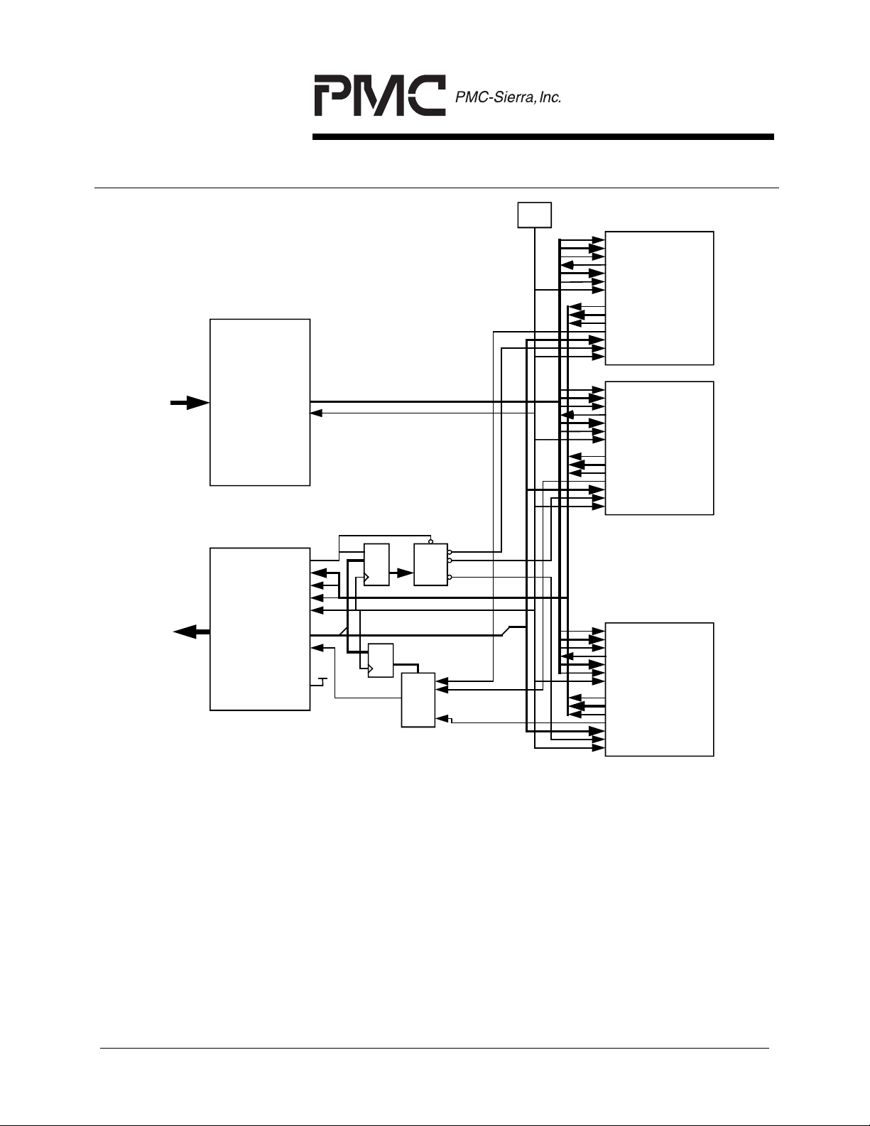
BLOCK DIAGRAM
IAV ALID/ICA[4]
IADDR[4:3]/ICA[3:2]
IADDR[2:0]/IW RENB[4:2]
1 or 2
SYSCLK
IDAT[7:0]
IPR TY
ISO C
IFCLK
ICA[1]
IWRENB[1]
IPO LL
ONESEC
S
I
O
K
M
D
T
TC
T
TD
JTAG Test
Access
Port
Input
FIFO
All Blocks
Microprocessor
Interface
B
T
S
TR
0]
SA[19:
External
RAM
Address
Lookup
G
N
O
C
Micro
Cell
Buffer
Cell
Processor
To External RAM
,
0]
RAM
SD[39:0]
SP[4:
Output
YB
BUS
FIFO
B
WB
OE
SADS
SR
S
Microprocessor
Arbitration
ODAT[7:0]
OPRTY
OSOC
OFCLK
OCA
ORDENB
OTSEN
face
ATM Cells)
Interface
Ut opia L e v e l
]
A[6:0
D[15:0]
ALE
CSB
B
T
TB
RDB
IN
WRB
RS
Q
E
R
D
Proprietary and Confidential to PMC-Sierra, Inc. 9
and for its Customer’s Internal Use.
(appended
SCI-PHY + Inter
Page 21

STANDARD PRODUCT
DATASHEET
PMC-960543 ISSUE 2 ROUTING CONTROL, MONITORING, & POLICING
PM7323 RCMP-200
200 MBPS
6
DESCRIPTION
The PM7322 Routing Control, Monitoring and Policing 200 Mbps (RCMP-200)
device is a monolithic integrated circuit that implements ATM layer functions that
include fault and performance monitoring, header translation and cell rate
policing. The RCMP-200 is intended to be situated between a switch core and
the physical layer devices in the ingress direction. The RCMP-200 supports a
sustained aggregate throughput of 0.355x10⁶ cells/s. The RCMP-200 uses
external SRAM to store per-VPI/VCI data structures. The device is capable of
supporting up to 65536 connections.
The Input Cell Interface can be connected to up to 32 physical layer devices
through a SCI-PHY compatible bus. The 53 byte ATM cell is encapsulated in a
data structure which can contain pre-pended or post-pended routing information.
Received cells are buffered in a four cell deep FIFO. All Physical Layer and
unassigned cells are discarded. For the remaining cells, a subset of ATM header
and appended bits is used as a search key to find the VC Table Record for the
virtual connection. If a connection is not provisioned and the search terminates
unsuccessfully as a result, the cell is discarded and a count of invalid cells is
incremented. If the search is successful, subsequent processing of the cell is
dependent on contents of the cell and configuration fields in the VC Table
Record.
The RCMP-200 performs header translation if so configured. The ATM header is
replaced by contents of fields in the VC Table Record for the connection. The VCI
contents are passed through transparently for VPCs. Appended bytes can be
replaced, added or removed.
If the RCMP-200 is the end point for a F4 or F5 OAM stream, the OAM cells are
dropped and processed. If the RCMP-200 is not the end point, the OAM cells
are passed to the Output Cell Interface with an optional copy passed to the
Microprocessor Cell Buffer. The reception of an AIS or RDI cell results in the
appropriate alarm. Upon the arrival of a Forward Monitoring or
Monitoring/Reporting cell, error counts are updated and a Backward Reporting
cell is optionally generated. Activate/Deactivate cells are passed to the
Microprocessor Cell Buffer for external processing. Continuity Check cells can
be generated if no user cells have been received in the latest 1.5 +/- 0.5 or 2.5
+/- 0.5 (default) seconds.
Proprietary and Confidential to PMC-Sierra, Inc. 10
and for its Customer’s Internal Use.
Page 22

STANDARD PRODUCT
DATASHEET
PMC-960543 ISSUE 2 ROUTING CONTROL, MONITORING, & POLICING
PM7323 RCMP-200
200 MBPS
Cell rate policing is supported through two instances of the Generic Cell Rate
Algorithm (GCRA) for each connection. Each cell that violates the traffic contract
can be tagged (CLP bit set high) or discarded. To allow full flexibility, each GCRA
instance can be programmed to police any combination of user cells, OAM cells,
Resource Management, high priority cells or low priority cells.
The RCMP-200 supports multicasting. A single received cell can result in an
arbitrary number of cells presented on the Output Cell Interface, each with its
own unique VPI/VCI value and appended bytes. The ATM cell payload is
duplicated without modification.
The Output Cell Interface can be connected to the switch core through an
extended cell format SCI-PHY compatible bus. Cells are stored in a four cell
deep FIFO until the downstream devices are ready to accept them. The details
of how cells are handled in this FIFO depends on the particular application of the
RCMP-200 and are presented in "Operational Modes" section.
The Microprocessor Interface is provided for device configuration, control and
monitoring by an external microprocessor. This interface provides access to the
external SRAM to allow creation of the data structure, configuration of individual
connections and monitoring of the connections. The Microprocessor Cell Buffer
gives access to the cell stream, either directly or through intervention by a DMA
controller. Programmed cell types can be routed to a microprocessor readable
sixteen cell FIFO. The microprocessor can send cells over the Output Cell
Interface.
The RCMP-200 is implemented in low power, 0.6 micron, +5 Volt CMOS
technology. It has TTL compatible inputs and outputs and is packaged in a 240
pin copper slugged plastic QFP package.
Proprietary and Confidential to PMC-Sierra, Inc. 11
and for its Customer’s Internal Use.
Page 23
STANDARD PRODUCT
PM7323 RCMP-200
DATASHEET
PMC-960543 ISSUE 2 ROUTING CONTROL, MONITORING, & POLICING
200 MBPS
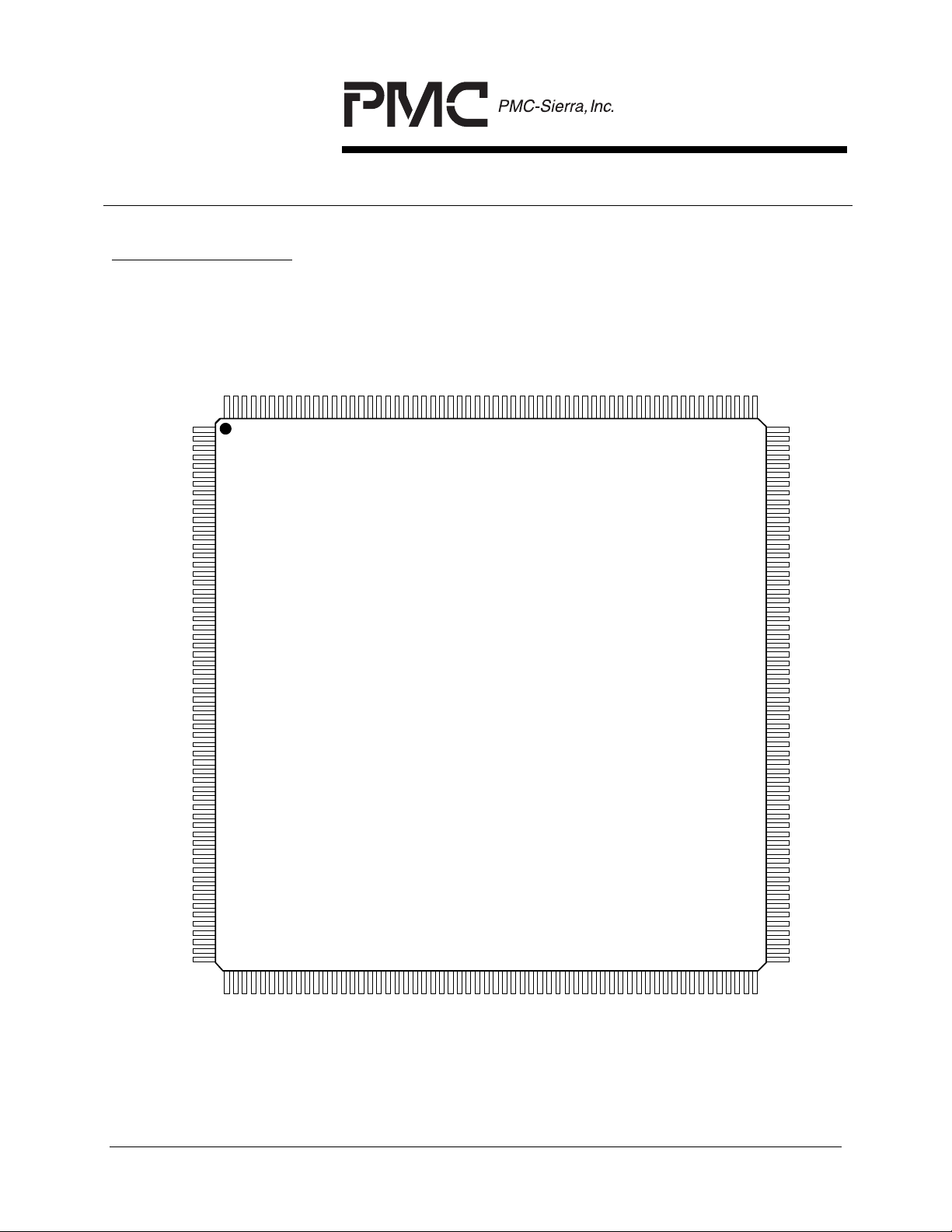
7
PIN 1
VSS_DC
VSS_DC
VSS_DC
VSS_DC
VSS_DC
VSS_DC
VSS_DC
VSS_DC
VDD_DC
VSS_DC
VSS_DC
IAVALID/ICA[4]
IADDR[4]/ICA[3]
VDD_AC
VSS_AC
IADDR[3]/ICA[2]
IADDR[2]/IWRENB[4]
IADDR[1]/IWRENB[3]
VDD_DC
VSS_DC
IADDR[0]/IWRENB[2]
IWRENB[1]
VDD_DC
VDD_AC
VSS_AC
VDD_DC
VSS_DC
VDD_DC
VSS_DC
VDD_DC
VSS_DC
VDD_AC
VSS_AC
PIN 60
PIN DIAGRAM
The RCMP-200 is packaged in a 240 pin slugged plastic QFP package having a
body size of 32 mm by 32 mm and a pin pitch of 0.5 mm.
SA[10]
VSS_DC
VDD_DC
SOEB
SADSB
SRWB
PIN 181
PIN 180
NC
VSS_AC
VDD_AC
SA[9]
SA[8]
SA[7]
SA[6]
SA[5]
SA[4]
VSS_AC
VDD_AC
VSS_DC
VDD_DC
SA[3]
SA[2]
SA[1]
SA[0]
SD[15]
SD[14]
SD[13]
VDD_AC
VSS_AC
VSS_DC
VDD_DC
SD[12]
SD[11]
SD[10]
SD[9]
SD[8]
VSS_AC
VDD_AC
VSS_DC
VDD_DC
SYSCLK
NC
NC
NC
VSS_DC
VDD_DC
SP[1]
SD[7]
SD[6]
SD[5]
SD[4]
SD[3]
VSS_AC
VDD_AC
SD[2]
SD[1]
SD[0]
SP[0]
NC
VSS_DC
VDD_DC
OFCLK
VSS_DC
VDD_DC
CONG
OTSEN
NC
PIN 121
IDAT[7]
IDAT[6]
IDAT[5]
IDAT[4]
IDAT[3]
IDAT[2]
IDAT[1]
IDAT[0]
IPRTY
ISOC
ICA[1]
IPOLL
IFCLK
TCK
TMS
TDO
TRSTB
D[0]
D[1]
D[2]
D[3]
D[4]
D[5]
D[6]
D[7]
SD[37]
VDD_AC
SD[34]
VDD_DC
SD[33]
SD[32]
SP[4]
SD[31]
SD[30]
VDD_AC
VSS_AC
SD[29]
SD[28]
SD[27]
SD[26]
VSS_DC
SD[25]
SD[24]
SP[3]
VDD_DC
VDD_AC
VSS_AC
SD[23]
SD[22]
SD[21]
SD[20]
SD[19]
SD[18]
SD[17]
VSS_AC
VSS_DC
VDD_AC
VDD_DC
SD[16]
SP[2]
SA[18]
SA[19]
SA[17]
SA[16]
SA[15]
VSS_AC
SA[14]
SA[13]
VDD_AC
SA[11]
SA[12]
VSS_AC
SD[36]
SD[35]
VSS_DC
VSS_DC
SD[39]
PIN 240
SD[38]
VDD_DC
NC
Pin 1 Index
PM7323
RCMP-200
TOP VIEW
TDI
A[0]
A[5]
A[4]
A[3]
A[2]
A[1]
VDD_DC
VSS_DC
ALE
RSTB
ONESEC
A[6]
D[8]
PIN 61
D[9]
D[10]
D[11]
VDD_AC
VSS_AC
VDD_DC
D[12]
VSS_DC
D[13]
D[14]
D[15]
INTB
DREQ
BUSYB
RDB
WRB
CSB
Proprietary and Confidential to PMC-Sierra, Inc. 12
and for its Customer’s Internal Use.
DNC
DNC
DNC
DNC
VDD_DC
VSS_DC
DNC
DNC
VSS_AC
VDD_AC
DNC
DNC
ODAT[6]
ODAT[7]
ODAT[5]
ODAT[4]
ODAT[3]
VDD_DC
VSS_AC
VDD_AC
VSS_DC
ODAT[1]
ODAT[2]
DNC
ODAT[0]
OSOC
OPRTY
OCA
ORDENB
VDD_DC
PIN 120
Page 24

STANDARD PRODUCT
DATASHEET
PMC-960543 ISSUE 2 ROUTING CONTROL, MONITORING, & POLICING
PM7323 RCMP-200
200 MBPS
8
PIN DESCRIPTION (TOTAL 240)
Table 1 - Output Cell Interface Signals (24)
Pin Name Type Pin
Feature
No.
OFCLK Input 126 The output FIFO clock (OFCLK) is used to read
words from the Output Cell Interface. OFCLK
must cycle at a 25 MHz or lower instantaneous
rate, but at a high enough rate to avoid FIFO
overflow. OSOC, OCA, OPRTY and ODAT[7:0]
are updated on the rising edge of OFCLK.
ORDENB is sampled using the rising edge of
OFCLK.
ORDENB Input 119 The active low read enable (ORDENB) signal is
used to indicate transfers from the Output Cell
Interface. When ORDENB is sampled low using
the rising edge of OFCLK, a word is read from
the internal synchronous FIFO and output on bus
ODAT[7:0]. When ORDENB is sampled high
using the rising edge of OFCLK, no read is
performed and outputs ODAT[7:0], OPRTY and
OSOC are tristated if the OTSEN input is high.
ORDENB must operate in conjunction with
OFCLK to access the FIFO at a high enough
instantaneous rate as to avoid FIFO overflows.
ODAT[0]
ODAT[1]
ODAT[2]
ODAT[3]
ODAT[4]
ODAT[5]
ODAT[6]
ODAT[7]
Tristate 114
113
112
107
106
105
104
103
The output cell data (ODAT[7:0]) bus carries the
ATM cell octets that are read from the output
FIFO. If the IBUS8 input is high, only ODAT[7:0]
carries cell octets. The ODAT[7:0] bus is updated
on the rising edge of OFCLK.
When the Output Cell Interface is configured for
tristate operation using the OTSEN input,
tristating of the ODAT[7:0] output bus is
controlled by the ORDENB input.
When OTSEN is low, the ODAT[7:0] bus is low
when no cell is being transferred.
Proprietary and Confidential to PMC-Sierra, Inc. 13
and for its Customer’s Internal Use.
Page 25

STANDARD PRODUCT
DATASHEET
PMC-960543 ISSUE 2 ROUTING CONTROL, MONITORING, & POLICING
PM7323 RCMP-200
200 MBPS
Pin Name Type Pin
Feature
No.
OPRTY Tristate 116 The output parity (OPRTY) signals indicate the
parity of the ODAT[7:0] bus. Odd or even parity
selection can be made using a register bit.
OPRTY is updated on the rising edge of OFCLK.
When the Output Cell Interface is configured for
tristate operation using the OTSEN input,
tristating of the OPRTY output bus is controlled
by the ORDENB input.
OSOC Tristate 117 The output start of cell (OSOC) signal marks the
start of cell on the ODAT[7:0] bus. When OSOC
is high, the first word of the cell structure is
present on the ODAT[7:0] stream. OSOC is
updated on the rising edge of OFCLK.
When the Output Cell Interface is configured for
tristate operation using the OTSEN input,
tristating of the OSOC output is controlled by the
ORDENB input.
OCA Output 118 The active polarity of this signal is programmable
and defaults to active high.
OCA indicates when a cell is available in the
output FIFO. When asserted, the OCA signal
indicates that the output FIFO has at least one
cell available to be read. The OCA signal is
deasserted when the output FIFO contains four
or zero words available for the current cell.
Selection is made using the OCALEVEL0 bit in
the Output FIFO Configuration register. OCA is
updated on the rising edge of OFCLK.
OTSEN Input 122 The tristate enable (OTSEN) signal allows tristate
control over the ODAT[7:0], OPRTY and OSOC
outputs. When OTSEN is high, the active low
read enable input, ORDENB, controls when the
ODAT[7:0], OPRTY and OSOC outputs are
driven. When OTSEN is low, the ODAT[7:0],
OPRTY and OSOC outputs are always driven.
Proprietary and Confidential to PMC-Sierra, Inc. 14
and for its Customer’s Internal Use.
Page 26

STANDARD PRODUCT
DATASHEET
PMC-960543 ISSUE 2 ROUTING CONTROL, MONITORING, & POLICING
PM7323 RCMP-200
200 MBPS
Pin Name Type Pin
Feature
No.
Table 2 - Input Cell Interface Signals (30)
Pin Name Type Pin
Feature
No.
IFCLK Input 41 The input FIFO clock (IFCLK) is used to write
words to the synchronous FIFO interface.
IFCLK must cycle at a 25 MHz or lower
instantaneous rate. ISOC, ICA[4:1], IPRTY and
IDAT[7:0] are sampled on the rising edge of
IFCLK. IWRENB[4:1], IADDR[4:0] and IAVALID
are updated on the rising edge of IFCLK.
IPOLL Input 35 The input polling select (IPOLL) pin determines
the method used to poll PHY devices.
If IPOLL is low, the IWRENB[4:1] and ICA[4:1]
signals are connected directly to up to four
single-PHY entities.
If IPOLL is high, polling using address lines is
used. The RCMP-200 uses the IADDR[4:0] and
IAVALID outputs to perform sequential polling of
the PHY devices to determine the next cell to
transfer.
Proprietary and Confidential to PMC-Sierra, Inc. 15
and for its Customer’s Internal Use.
Page 27

STANDARD PRODUCT
DATASHEET
PMC-960543 ISSUE 2 ROUTING CONTROL, MONITORING, & POLICING
PM7323 RCMP-200
200 MBPS
Pin Name Type Pin
No.
IWRENB[1]
IWRENB[2]
IWRENB[3]
IWRENB[4]
IADDR[4]
IADDR[3]
IADDR[2]
IADDR[1]
IADDR[0]
Output 34
33
30
29
I/O 24
27
29
30
33
Feature
The active low write enable (IWRENB[4:1])
inputs are used to initiate writes to the input
FIFO.
If the IPOLL input is low, the RCMP-200 asserts
one of the IWRENB[4:1] outputs to transfer a
cell from one of up to four PHY devices. A valid
word is expected on the IDAT[7:0] bus at the
second rising edge of IFCLK after one of the
enables is asserted low. When all of the enables
are high, no valid data is expected. The
IWRENB[4:1] outputs are updated on the rising
edge of IFCLK. See Figure 7.
If the IPOLL input is high, the IWRENB[4:2] pins
are redefined as IADDR[2:0]. The IWRENB[1]
pin is used to transfer all cells. The source PHY
is selected by the IADDR[4:0] signals.
If the IPOLL input is high, the IADDR[4:0] pins
are used for PHY addressing. If the IPOLL input
is low, the IADDR[4:0] pins are redefined as
ICA[3:2] and IWRENB[4:2].
If the IPOLL input is high, the IADDR[4:0]
signals are outputs and are used to address up
to 32 PHY devices for the purposes of polling
and selection for cell transfer. When conducting
polling, in order to avoid bus contention, the
RCMP-200 inserts gap cycles during which
IADDR[4:0] is set to 1F hex and IAVALID to logic
0. When this occurs, no PHY device should
drive ICA[1] during the following clock cycle.
Polling is performed in a incrementing sequential
order. The PHY device selected for transfer is
based on the IADDR[4:0] value present when
IWRENB[1] falls. The IADDR[4:0] bus is
updated on the rising edge of IFCLK.
Proprietary and Confidential to PMC-Sierra, Inc. 16
and for its Customer’s Internal Use.
Page 28

STANDARD PRODUCT
DATASHEET
PMC-960543 ISSUE 2 ROUTING CONTROL, MONITORING, & POLICING
PM7323 RCMP-200
200 MBPS
Pin Name Type Pin
Feature
No.
IAVALID I/O 23 If the IPOLL input is high, the PHY Address
Valid (IAVALID) pin is active. If the IPOLL input
is low, the IAVALID pin is redefined as ICA[4].
If the IPOLL input is high, the IAVALID pin
indicates that the IADDR[4:0] bus is outputting a
valid PHY address for polling purposes. When
this signal is deasserted, the IADDR[4:0] bus is
set to 1F hex.
IAVALID is not necessary when less than 32
PHY links are being polled.
IDAT[0]
IDAT[1]
IDAT[2]
IDAT[3]
IDAT[4]
IDAT[5]
IDAT[6]
IDAT[7]
Input 19
18
17
16
15
14
13
10
The input cell data (IDAT[7:0]) bus carries the
ATM cell octets that are written to the input
FIFO. The IDAT[7:0] bus is sampled on the
rising edge of IFCLK and is considered valid
only when one of the IWRENB[4:1] signals so
indicates.
IPRTY Input 21 The input parity (IPRTY) signals indicate the
parity of the IDAT[7:0] bus. Odd or even parity
selection can be made using a register. A
maskable interrupt status is generated upon a
parity error; no other actions are taken. IPRTY
is sampled on the rising edge of IFCLK and is
considered valid only when one of the
IWRENB[4:1] signals so indicates.
Proprietary and Confidential to PMC-Sierra, Inc. 17
and for its Customer’s Internal Use.
Page 29

STANDARD PRODUCT
DATASHEET
PMC-960543 ISSUE 2 ROUTING CONTROL, MONITORING, & POLICING
PM7323 RCMP-200
200 MBPS
Pin Name Type Pin
Feature
No.
ISOC Input 22 The input start of cell (ISOC) signal marks the
start of cell on the IDAT[7:0] bus. When ISOC is
high, the first word of the cell structure is present
on the IDAT[7:0] stream. It is not necessary for
ISOC asserted for each cell. An interrupt may
be generated if ISOC is high during any word
other than the first word of the cell structure.
ISOC is sampled on the rising edge of IFCLK
and is considered valid only when one of the
IWRENB[4:1] signals so indicates.
Proprietary and Confidential to PMC-Sierra, Inc. 18
and for its Customer’s Internal Use.
Page 30

STANDARD PRODUCT
DATASHEET
PMC-960543 ISSUE 2 ROUTING CONTROL, MONITORING, & POLICING
PM7323 RCMP-200
200 MBPS
Pin Name Type Pin
No.
ICA[1]
ICA[2]
ICA[3]
ICA[4]
I/O 28
27
24
23
Feature
The active polarity of these signals is
programmable and defaults to active high.
If the IPOLL input is low, the RCMP-200 asserts
the appropriate IWRENB[4:1] signal in response
to a round-robin polling of the ICA[4:1] signals.
Once committed, the RCMP-200 will transfer an
entire cell from a single physical link before
servicing the next. The RCMP-200 will complete
the read of an entire cell even if the associated
ICA[4:1] input is deasserted during the cell.
Sampling of ICA[4:1] resumes the cycle after the
last octet of a cell has been transferred.
Note that ICA[1] is an input only.
If the IPOLL input is high, the ICA[3:2] pins are
redefined as IADDR[4:3] and the ICA[4] pin is
redefined as IAVALID.
If the IPOLL input is high, the RCMP-200 polls
up to 32 PHY devices using the PHY address
signals IADDR[4:0]. A PHY device being
addressed by IADDR[4:0] is expected to indicate
whether or not it has a complete cell available
for transfer by driving ICA[1] during the clock
cycle following that in which it is addressed.
(When a cell transfer is in progress, the RCMP200 will not poll the PHY device which is
sending the cell and so PHY devices need not
support cell availability indication during cell
transfer.) The selection of a particular PHY
device from which to transfer a cell is indicated
by the state of IADDR[4:0] when IWRENB[1]
falls.
Note that ICA[1] is an input only.
Proprietary and Confidential to PMC-Sierra, Inc. 19
and for its Customer’s Internal Use.
Page 31

STANDARD PRODUCT
DATASHEET
PMC-960543 ISSUE 2 ROUTING CONTROL, MONITORING, & POLICING
PM7323 RCMP-200
200 MBPS
Table 3 - Synchronous SRAM Interface Signals (70)
Pin Name Type Pin
No.
SA[19]
SA[18]
SA[17]
SA[16]
SA[15]
SA[14]
SA[13]
SA[12]
SA[11]
SA[10]
SA[9]
SA[8]
SA[7]
SA[6]
SA[5]
SA[4]
SA[3]
SA[2]
SA[1]
SA[0]
Output 197
196
195
194
193
190
189
188
187
184
177
176
175
174
173
172
167
166
165
164
Feature
The SRAM Address (SA[19:0]) outputs identify
the SRAM location accessed.
The sixteen least significant bits (SA[15:0]
locate one of a possible 65536 VC Table
entries. If 65536 connections are not required,
the most significant bits of SA[15:0] may be
unconnected with no physical memory
associated with the unused memory space.
The four most significant bits (SA[19:16])
identify the fields within a VC Table Record. In
most applications, SA[19:16] is decoded to
SRAM chip selects. Physical memory need
not be allocated for unused fields.
The SA[15:0] outputs are also used to access
the Search Table.
The SA[19:0] bus is updated on the rising
edge of SYSCLK.
Proprietary and Confidential to PMC-Sierra, Inc. 20
and for its Customer’s Internal Use.
Page 32

STANDARD PRODUCT
DATASHEET
PMC-960543 ISSUE 2 ROUTING CONTROL, MONITORING, & POLICING
PM7323 RCMP-200
200 MBPS
Pin Name Type Pin
No.
SD[39]
SD[38]
SD[37]
SD[36]
SD[35]
SD[34]
SD[33]
SD[32]
SD[31]
SD[30]
SD[29]
SD[28]
SD[27]
SD[26]
SD[25]
SD[24]
SD[23]
SD[22]
SD[21]
SD[20]
SD[19]
SD[18]
SD[17]
SD[16]
SD[15]
SD[14]
SD[13]
SD[12]
SD[11]
SD[10]
SD[9]
SD[8]
SD[7]
SD[6]
SD[5]
SD[4]
SD[3]
SD[2]
SD[1]
SD[0]
I/O 238
237
236
233
232
229
228
227
225
224
221
220
219
218
217
214
210
209
208
207
206
205
204
199
163
162
161
156
155
154
153
152
140
139
138
137
136
133
132
131
Feature
The bi-directional SRAM Data (SD[39:0]) pins
interface directly with synchronous SRAM data
ports.
A SRAM read is perfor med when the RCMP200 drives the address strobe (SADSB) low
and the SRWB output high. The RCMP-200
tristates the SD[39:0] pins and samples the
value driven by the SRAM on the second rising
edge of the SYSCLK input after SADSB is
asserted.
A SRAM write is performed when RCMP-200
drives the address strobe (SADSB) low and
the SRWB output low. The RCMP-200
presents valid data on the SD[39:0] pins upon
the rising edge of SYSCLK which is written
into the SRAM on the next SYSCLK rising
edge. SD[39:0] is tri-stated on the rising edge
of SYSCLK. Contention is avoided by not
performing a read during the cycle after the
write burst.
Proprietary and Confidential to PMC-Sierra, Inc. 21
and for its Customer’s Internal Use.
Page 33

STANDARD PRODUCT
DATASHEET
PMC-960543 ISSUE 2 ROUTING CONTROL, MONITORING, & POLICING
PM7323 RCMP-200
200 MBPS
Pin Name Type Pin
Feature
No.
SP[4]
SP[3]
SP[2]
SP[1]
SP[0]
I/O 226
213
198
141
130
The SRAM Par ity (SP[4:0]) pins provide parity
protection over the SD[39:0] bus.
SP[4] completes odd parity for SD[39:32].
SP[3] completes odd parity for SD[31:24].
SP[2] completes odd parity for SD[23:16].
SP[1] completes odd parity for SD[15:8].
SP[0] completes odd parity for SD[7:0].
SP[4:0] has the same timing as SD[39:0].
When data is being written to the external
SRAM, the RCMP-200 generates correct
parity. When data is being read from the
external SRAM, the RCMP-200 checks the
parity and generates a maskable interrupt
indication upon an error. No other action is
taken; therefore, the SP[4:0] may be
unconnected if parity protection is not required.
SADSB Output 181 The SRAM Address Strobe (SADSB) qualifies
the address bus. If the SADSB output is
asserted low, an SRAM access is initiated.
SADSB is updated on the rising edge of
SYSCLK.
SOEB Output 183 The asynchronous SRAM Output Enable
(SOEB) controls the SRAM tri-state outputs.
When SOEB is low during a read cycle, the
selected SRAM (as determined by SA[19:0]
decoding) is expected to drive SD[39:0] and
SP[4:0].
SOEB is updated on the rising edge of
SYSCLK.
Proprietary and Confidential to PMC-Sierra, Inc. 22
and for its Customer’s Internal Use.
Page 34

STANDARD PRODUCT
DATASHEET
PMC-960543 ISSUE 2 ROUTING CONTROL, MONITORING, & POLICING
PM7323 RCMP-200
200 MBPS
Pin Name Type Pin
Feature
No.
SRWB Output 182 The SRAM read/write enable (SRWB)
determines the SRAM access type. SRWB is
qualified by the SADSB output. The RCMP200 drives the SRWB output high if the
subsequent cycle is a SRAM read. The
RCMP-200 drives the SRWB output low if the
current cycle is a SRAM write.
SRWB is updated on the rising edge of
SYSCLK.
Table 4 - Microprocessor Interface Signals (30)
Pin Name Type Pin
Feature
No.
CSB Input 78 CSB is low during RCMP-200 Microprocessor
Interface Port register accesses.
If CSB is not required (i.e. register accesses
controlled using the RDB and WRB signals
only), CSB should be connected to an inverted
version of the RSTB input.
RDB Input 76 RDB is low during RCMP-200 Microprocessor
Interface Port register read accesses. The
RCMP-200 drives the D[15:0] bus with the
contents of the addressed register while RDB
and CSB are low.
WRB Input 77 WRB is low during a RCMP-200
Microprocessor Interface Port register write
accesses. The D[15:0] bus contents are
clocked into the addressed register on the
rising WRB edge while CSB is low.
Proprietary and Confidential to PMC-Sierra, Inc. 23
and for its Customer’s Internal Use.
Page 35

STANDARD PRODUCT
DATASHEET
PMC-960543 ISSUE 2 ROUTING CONTROL, MONITORING, & POLICING
PM7323 RCMP-200
200 MBPS
Pin Name Type Pin
Feature
No.
DREQ Output 75 The DMA request (DREQ) output is asserted
when the Microprocessor Cell Buffer contains
a cell to be read and the DMAEN bit in the
Microprocessor Buffer Configuration register is
a logic 1. The first read of the Microprocessor
Cell Data register after DREQ is asserted will
return the first word of the cell. DREQ is
deasserted after the last word of the cell has
been read or an abort has been signaled.
The polarity of the DREQ output is
programmable and defaults to active high.
BUSYB Output 74 The BUSYB output is asserted while a µP
access request to the external SRAM is
pending. The BUSYB output is deasserted
after the access has been completed. A µP
access request is typically completed within 37
SYSCLK cycles. If the STANDBY bit in the
Master Configuration is a logic 1, the access
time is reduced to less than 5 SYSCLK cycles.
The polarity of the BUSYB output is
programmable and defaults to active low.
The BUSYB should be treated as a glitch-free
asynchronous output.
Proprietary and Confidential to PMC-Sierra, Inc. 24
and for its Customer’s Internal Use.
Page 36

STANDARD PRODUCT
DATASHEET
PMC-960543 ISSUE 2 ROUTING CONTROL, MONITORING, & POLICING
PM7323 RCMP-200
200 MBPS
Pin Name Type Pin
No.
D[0]
D[1]
D[2]
D[3]
D[4]
D[5]
D[6]
D[7]
D[8]
D[9]
D[10]
D[11]
D[12]
D[13]
D[14]
D[15]
A[0]
A[1]
A[2]
A[3]
A[4]
A[5]
A[6]/TRS
I/O 49
50
51
52
57
58
59
60
61
62
63
64
69
70
71
72
Input 90
89
88
87
86
85
84
Feature
The bi-directional data bus D[15:0] is used
during RCMP-200 Microprocessor Interface
Port register read and write accesses. D[15:8]
should contain the most significant byte of a
word while D[7:0] should contain the least
significant byte of a word.
A[6:0] selects specific Microprocessor
Interface Port registers during RCMP-200
register accesses. A[6] is the Test Register
Select (TRS) address pin. TRS selects
between normal and test mode register
accesses. TRS is high during test mode
register accesses, and is low during normal
mode register accesses.
ALE Input 83 ALE is active high and latches the address bus
A[6:0] when low. When ALE is high, the
internal address latches are transparent. It
allows the RCMP-200 to interface to a
multiplexed address/data bus. ALE has an
integral pull up resistor.
INTB OD
Output
73 The interrupt request (INTB) output goes low
when a RCMP-200 interrupt source is active
and that source is unmasked. INTB returns
high when the interrupt is acknowledged via an
appropriate register access. INTB is an open
drain output.
Proprietary and Confidential to PMC-Sierra, Inc. 25
and for its Customer’s Internal Use.
Page 37

STANDARD PRODUCT
DATASHEET
PMC-960543 ISSUE 2 ROUTING CONTROL, MONITORING, & POLICING
PM7323 RCMP-200
200 MBPS
Table 5 - Misc. Interface Signals (66)
Pin Name Type Pin
Feature
No.
SYSCLK Input 147 The system clock (SYSCLK) provides timing
for the RCMP-200's internal circuitry. SYSCLK
should be nominally a 50% duty cycle 25 MHz
to 52 MHz clock. SYSCLK should be
connected to the same clock buffer as the
external synchronous SRAM clock.
CONG Input 123 The congestion indication (CONG) input
signals that cell congestion is occurring in an
element downstream of the RCMP-200 and
that all low priority cells be dropped. If CONG
is high, the RCMP-200 drops all cells with a
one in the CLP bit position after policing has
occurred, except AAL5 end-of-message (EOM)
cells. (Dropping an EOM cell results in
corrupting two packets; this does help to
relieve the congestion.)
CONG may be treated as an asynchronous
input.
ONESEC Input 81 The one second clock (ONESEC) provides
precise timing for events such as the
generation of RDI and AIS cell and the
clearing of AIS, RDI and Continuity Check
alarms.
By default, the initiation of one second events
is based on the SYSCLK period; therefore, the
ONESEC input is ignored. If the SEL1SEC
register bit is a logic 1, the ONESEC input
becomes the source of the one second clock.
ONESEC must be glitch free and may be
treated as an asynchronous input.
Proprietary and Confidential to PMC-Sierra, Inc. 26
and for its Customer’s Internal Use.
Page 38

STANDARD PRODUCT
DATASHEET
PMC-960543 ISSUE 2 ROUTING CONTROL, MONITORING, & POLICING
PM7323 RCMP-200
200 MBPS
Pin Name Type Pin
Feature
No.
RSTB Scmitt
Trigger
Input
Internal
Pull-up
82 The active low reset (RSTB) signal provides an
asynchronous RCMP-200 reset. RSTB is a
Schmitt triggered input with an integral pull up
resistor. When RSTB is forced low, all RCMP200 registers are forced to their default states.
TCK Input 44 The test clock (TCK) signal provides timing for
test operations that can be carried out using
the IEEE P1149.1 test access port.
TMS Input
Internal
Pull-up
45 The test mode select (TMS) signal controls the
test operations that can be carried out using
the IEEE P1149.1 test access port. TMS is
sampled on the rising edge of TCK. TMS has
an integral pull up resistor.
TDI Input
Internal
Pull-up
46 The test data input (TDI) signal carries test
data into the RCMP-200 via the IEEE P1149.1
test access port. TDI is sampled on the rising
edge of TCK. TDI has an integral pull up
resistor.
TDO Tristate 47 The test data output (TDO) signal carries test
data out of the RCMP-200 via the IEEE
P1149.1 test access port. TDO is updated on
the falling edge of TCK. TDO is a tri-state
output which is tri-stated except when
scanning of data is in progress.
TRSTB Scmitt
Trigger
Input
Internal
Pull-up
48 The active low test reset (TRSTB) signal
provides an asynchronous RCMP-200 test
access port reset via the IEEE P1149.1 test
access port. TRSTB is a Schmitt triggered
input with an integral pull up resistor.
The JTAG TAP controller must be initialized
when the RCMP-200 is powered up. If the
JTAG port is not used TRSTB must be
connected to the RSTB input or VSS.
Proprietary and Confidential to PMC-Sierra, Inc. 27
and for its Customer’s Internal Use.
Page 39

STANDARD PRODUCT
DATASHEET
PMC-960543 ISSUE 2 ROUTING CONTROL, MONITORING, & POLICING
PM7323 RCMP-200
200 MBPS
Pin Name Type Pin
No.
VDD_DC1
VDD_DC2
VDD_DC3
VDD_DC4
VDD_DC5
VDD_DC6
VDD_DC7
VDD_DC8
VDD_DC9
VDD_DC10
VDD_DC11
VDD_DC12
VDD_DC13
VDD_DC14
VDD_DC15
VDD_DC16
VDD_DC17
VDD_DC18
VDD_DC19
VDD_DC20
VDD_DC21
VDD_DC22
Power
11
31
36
39
42
53
67
79
94
108
120
124
127
142
148
157
168
185
200
215
230
239
Feature
The DC power (VDD_DC1 - VDD_DC2 2) pins
should be connected to a well-decoupled +5 V
DC supply in common with VDD_AC.
Proprietary and Confidential to PMC-Sierra, Inc. 28
and for its Customer’s Internal Use.
Page 40

STANDARD PRODUCT
DATASHEET
PMC-960543 ISSUE 2 ROUTING CONTROL, MONITORING, & POLICING
PM7323 RCMP-200
200 MBPS
Pin Name Type Pin
No.
VSS_DC1
VSS_DC2
VSS_DC3
VSS_DC4
VSS_DC5
VSS_DC6
VSS_DC7
VSS_DC8
VSS_DC9
VSS_DC10
VSS_DC11
VSS_DC12
VSS_DC13
VSS_DC14
VSS_DC15
VSS_DC16
VSS_DC17
VSS_DC18
VSS_DC19
VSS_DC20
VSS_DC21
VSS_DC22
VSS_DC23
VSS_DC24
VSS_DC25
VSS_DC26
VSS_DC27
VSS_DC28
VSS_DC29
Ground
2
3
4
5
6
7
8
9
12
20
32
40
43
54
68
80
95
109
125
128
143
149
158
169
186
201
216
231
240
Feature
The DC ground (VSS_DC1 - VSS_DC29) pins
should be connected to GND in common with
VSS_AC.
Proprietary and Confidential to PMC-Sierra, Inc. 29
and for its Customer’s Internal Use.
Page 41

STANDARD PRODUCT
DATASHEET
PMC-960543 ISSUE 2 ROUTING CONTROL, MONITORING, & POLICING
PM7323 RCMP-200
200 MBPS
Pin Name Type Pin
No.
VDD_AC1
VDD_AC2
VDD_AC3
VDD_AC4
VDD_AC5
VDD_AC6
VDD_AC7
VDD_AC8
VDD_AC9
VDD_AC10
VDD_AC11
VDD_AC12
VDD_AC13
VDD_AC14
VDD_AC15
VDD_AC16
VSS_AC1
VSS_AC2
VSS_AC3
VSS_AC4
VSS_AC5
VSS_AC6
VSS_AC7
VSS_AC8
VSS_AC9
VSS_AC10
VSS_AC11
VSS_AC12
VSS_AC13
VSS_AC14
VSS_AC15
VSS_AC16
Power
Ground
25
37
55
65
98
110
134
150
160
170
178
191
202
211
222
234
26
38
56
66
99
111
135
151
159
171
179
192
203
212
223
235
Feature
The AC power (VDD_AC1 - VDD_AC16) pins
should be connected to a well-decoupled +5 V
DC supply in common with VDD_DC.
The AC ground (VSS_AC1 - VSS_AC16) pins
should be connected to GND in common with
VSS_DC.
Proprietary and Confidential to PMC-Sierra, Inc. 30
and for its Customer’s Internal Use.
Page 42

STANDARD PRODUCT
DATASHEET
PMC-960543 ISSUE 2 ROUTING CONTROL, MONITORING, & POLICING
PM7323 RCMP-200
200 MBPS
Pin Name Type Pin
No.
DNC1
DNC2
DNC3
DNC4
DNC5
DNC6
DNC7
DNC8
DNC9
NC1
NC2
NC3
NC4
NC5
NC6
NC7
do not
connect
no
connect
91
92
93
96
97
100
101
102
115
1
122
129
144
145
146
180
Notes on Pin Description:
Feature
Do not connect these pins.
It is required that
these pins not be connected. Connection to
them may result in erroneous behaviour under
normal operating conditions.
These pins are not connected.
1. All RCMP-200 inputs and bi-directionals present minimal capacitive loading
and operate at TTL logic levels.
2. All RCMP-200 digital outputs and bi-directionals have 2 mA D.C. drive
capability.
3. Inputs RSTB, TRSTB, TMS, TDI and ALE have internal pull-up resistors.
4. The VSS_DC and VSS_AC ground pins are not internally connected together.
Failure to connect these pins externally may cause malfunction or damage
the RCMP-200.
5. The VDD_DC and VDD_AC power pins are not internally connected together.
Failure to connect these pins externally may cause malfunction or damage
the RCMP-200.
Proprietary and Confidential to PMC-Sierra, Inc. 31
and for its Customer’s Internal Use.
Page 43

STANDARD PRODUCT
DATASHEET
PMC-960543 ISSUE 2 ROUTING CONTROL, MONITORING, & POLICING
PM7323 RCMP-200
200 MBPS
9
FUNCTIONAL DESCRIPTION
The RCMP-200 receives cells from up to 32 PHY devices, processes them, and
passes them to a single switch port or queue manager. The RCMP-200 device
operates as a multi-PHY master on its input side. Round-robin polling selects
between the PHY devices based on the availability of cells.
The Output Cell Interface operates as a single-PHY slave. The RCMP-200
informs the bus master if it has a cell available for transfer out by asserting OCA,
and waits for the bus master to assert the ORDENB signal to effect the transfer.
If the output buffer becomes full, the RCMP-200 will apply back-pressure to all its
input PHYs.
Logical multicasting is possible, although the system design must take into
account the fact that the input PHYs may be backed-up as a result - with possible
cell loss occurring.
9.1 Input Buffering
Cells received on the extended cell format SCI-PHY compatible Input Cell
Interface are buffered in a 4 cell deep FIFO. The input buffer provides for the
separation of internal timing from asynchronous external devices.
The SCI-PHY cell interface operates at clock rates up to 25 MHz and supports 8
bit wide data structures with programmable lengths. The data structure contains
a 52 (HEC excluded) or 53 byte ATM cell and up to 10 appended bytes. The
start of the data structure is indicated by the ISOC input. Refer to the
"Operation" section for more detail on this data structure. The data bus is
protected by the IPRTY input. The parity can be configured to be odd or even.
The input FIFO filters all unassigned cells and cells reserved for the use of the
Physical Layer. Unassigned cells are identified by an all zero VPI/VCI value and
CLP=0. They are filtered without notification. Physical layer cells are identified
by an all zero VPI/VCI value and CLP=1. They are filtered with a resulting
maskable interrupt indication and a Physical Layer cell count increment. By
default, the cell coding is assumed to be for a Network-Network Interface (NNI);
therefore the VPI is taken to be twelve bits. If one of the PHY links is a UserNetwork Interface (UNI) and the GFC field is non-zero, the cell will not be filtered
by the Input Cell Interface, but will be discarded by the VC Identification circuit.
As an option, all cells can be interpreted as UNI cells.
Proprietary and Confidential to PMC-Sierra, Inc. 32
and for its Customer’s Internal Use.
Page 44

STANDARD PRODUCT
DATASHEET
PMC-960543 ISSUE 2 ROUTING CONTROL, MONITORING, & POLICING
PM7323 RCMP-200
200 MBPS
The RCMP-200 is a bus master and services the PHY devices in one of two
ways: direct status arbitration or address line polling. For direct status arbitration,
the RCMP-200 monitors cell available signals (ICA[4:1]) from to up four physical
(PHY) layer devices and generates write enables (WRENB[4:1]) in response. For
address line polling, ICA[1] and IWRENB[1] are shared between up to 32 PHY
devices and signals IADDR[4:0] and IAVALID are used to address the latter
individually. The RCMP-200 performs round-robin polling of the PHY devices to
determine which have available cells. The RCMP-200 will read an entire cell
from one PHY device before accessing the next PHY device. No fixed cell slots
exist, but instead the RCMP-200 maximizes throughput by servicing a PHY
device as soon as the bus is free and PHY device's cell available signal is
asserted.
All input FIFO signals, ISOC, IWRENB[4:1], ICA[4:1], IADDR[4:0], IAVALID,
IPRTY and IDAT[7:0] are either sampled or updated on the rising edge of the
IFCLK clock input.
9.2 VC Identification
The RCMP-200 makes use of a flexible approach to identify incoming cells and
to determine which record in the VC Table they are associated with. The RCMP200 is able to identify each cell's VC by searching the
Table 6) using selected portions of the cell header, prepend, postpend along
with the cell's PHY address. To do this, the RCMP-200 creates an internal
Routing Wor d
which is the concatenation of the cell header, cell prepend and
cell postpend. The RCMP-200 is programmed to select portions of the Routing
Word plus the PHY address to create a
therefore, consists of portions of the cell's header, prepend, postpend and SCIPHY address. See Figure 3.
Figure 3 is not intended to imply any restrictions on the positioning of Field A and
Field B. These fields may occur any where within the appended octets or the
ATM header. The Primary Key and Secondary Key may also intersect.
VC Search Key
VC Search Table
(see
. The VC Search key,
Proprietary and Confidential to PMC-Sierra, Inc. 33
and for its Customer’s Internal Use.
Page 45

STANDARD PRODUCT
DATASHEET
PMC-960543 ISSUE 2 ROUTING CONTROL, MONITORING, & POLICING
PM7323 RCMP-200
200 MBPS
Figure 3 - VC Search Key Composition
Routing Word
Cell Prepend Cell Postpend Cell Header
m
Field A Field B
S
S - L
AA
A
length <= 128 bits
BB
S - L
B
VPI/VCI
(NNI)
47S
(UNI)
43
20
HEC UDF
0
VC Search Key
PHY
Primary Key Secondary Key
Field A Field B VPI/VCI
ID
The RCMP-200 divides the VC Search Key into two search keys - the Primary
Search Key and the Secondary Search Key. The Primary Key is 0 to 16 bits long.
It is constructed from two fields - the
PHY ID
and
Field A
. The PHY ID field and
Field A can be programmed to be 0-5 bits and 0-16 bits long, respectively. The
PHY ID is the SCI-PHY address and must, therefore, include sufficient bits to
encode all the PHYs at the PHY Layer interface of the RCMP-200. Field A starts
at location SA of the Routing Word and has length LA. The number of bits in
Field A plus the number in the PHY ID field must be less than or equal to 16.
The Secondary Search Key is 39 bits long and is composed of two fields. The
first field,
Field B
, is 0 to 11 bits long and may start anywhere in the routing
word. Field B parameters include starting position SB, and length LB. The second
field is the 28 bit VCI/VPI. This field is always taken from the cell's header.
Proprietary and Confidential to PMC-Sierra, Inc. 34
and for its Customer’s Internal Use.
Page 46

STANDARD PRODUCT
DATASHEET
PMC-960543 ISSUE 2 ROUTING CONTROL, MONITORING, & POLICING
PM7323 RCMP-200
200 MBPS
Field B and the VPI/VCI field are positioned "right justified" within the routing
word.
Figure 4 - Parameters of Primary Key and Secondary Key
Primary Key
PHY ID Field A
L
P
0-5 bits
+
L
L
P
0-16 bits
<= 16 bits
A
L
A
Secondary Key
Unused
0-11 bits
Field B
L
B
0-11 bits 28 bits
L
+
B
+ Unused
28
= 39 bits
VPI / VCI
The user can program the RCMP-200 with the length and position parameters of
fields A and B. Refer to the descriptions for registers 0x28 and 0x29. N.B. Lp =
binary length of the PHYID field, as given by the coding of the PHY[2:0] register
bits.
Figure 5 provides a representation of how the RCMP-200 creates the Primary
and Secondary search keys. Field location and length registers are used to
select Field A and Field B from the routing word. Field A and the PHYID are
concatenated to form the Primary Search Key. Field B and the VPI/VCI field are
concatenated to form the secondary search key.
Proprietary and Confidential to PMC-Sierra, Inc. 35
and for its Customer’s Internal Use.
Page 47

STANDARD PRODUCT
DATASHEET
PMC-960543 ISSUE 2 ROUTING CONTROL, MONITORING, & POLICING
PM7323 RCMP-200
200 MBPS
Figure 5 - Construction of Search Keys
CONFIGURATION
REGISTERS
Field B
Location
Registers
Field A
Location
Registers
SB,L
SA,L
B
A
Field B Size & Location
Field A Size
& Location
VPI/VCI
ROUTING
WORD
Field A
PHY ID
PRIMARY
SEARCH KEY
Field B
VCI/VPI
SECONDARY
SEARCH KEY
Once the search keys are assembled, the Primary Search Key is first used to
address an external direct look-up table (
Primary T ab le
). This table occupies 2
n
memory locations where n = LP + LA, i.e. the length of the Primary Search Key.
The result of this direct look up is the address of a root node of a search tree.
From this root node, the Secondary Search Key is used by a patented search
algorithm to find the cell's VC Table address (held in external SRAM.) The
RCMP-200 requires this table address for cell processing. Table 1 provides a
description of the VC Table. If the search process does not lead to the successful
identification of the cell concerned (contents of the VC table address returned do
not match the Secondary Search Key contents), the cell is discarded as invalid.
Optionally, the cell is routed to the microprocessor cell interface for header error
logging.
The length of time required to perform the VC search is variable. Since the
Primary Search Key is used in a direct look up, only one cycle is required to
process the Primary Key. The Secondary Search Key processing time is highly
dependent on the key's contents, but the maximum number of processing cycles
Proprietary and Confidential to PMC-Sierra, Inc. 36
and for its Customer’s Internal Use.
Page 48

STANDARD PRODUCT
DATASHEET
PMC-960543 ISSUE 2 ROUTING CONTROL, MONITORING, & POLICING
PM7323 RCMP-200
200 MBPS
required is equal to the number of bits in the Secondary Search Key which must
the examined to make a unique identification. Some VPI and VCI bits may
always be zero; therefore, they need not be used in the search. In some
instances, the Primary Search Key may over lap the Secondary Search Key;
therefore, the intersecting bits are only required for the confirmation of a search
and will not be used as decision points by the binary search. If the number of
bits used by the binary search is no greater than 18, a sustained rate of
0.355x10⁶ cell/s is guaranteed. The general expression for guaranteed
throughput is
Throughput
=
(17+ max.binary tree depth)(SYSCLK period)
1
cell / s
Note, however, if the binary tree depth is is less than 10, the throughput
becomes:
Throughput
=
(cell word length)(SYSCLK period)
1
cell / s
where the cell word length is the number of 8-bit words in the cell.
The first two words of each VC Table Record are reserved for the primary table
and the search table. The third word of the VC Table Record contains the
Secondary Search Key and an "NNI" bit in the most significant bit position. This
word is used to confirm whether the incoming cell belongs to a provisioned
virtual connection. Any unused bits within this word must be set to zero. The
NNI bit identifies if the VC belongs to a Network-Network Interface. If the NNI bit
is set to zero, the connection is part of a UNI which means that the four MSBs of
the VPI are excluded from the secondary key ver ification. If the VCI field in the
VC Table is all zeros, this signifies the connection is a VPC and that the VCI field
is to be ignored.
9.2.1 Search Ta ble Data Structure
The Primary and Secondary Search Tables reside in external SRAM. The
Primary Search Table is located in the least significant 16 bits of RAM locations
with SA[19:16]=0001 and requires 2
(LP + LA)
Search Table resides in RAM locations with SA[19:16]=0000 and its size is
bounded by the number of virtual connections supported.
Proprietary and Confidential to PMC-Sierra, Inc. 37
and for its Customer’s Internal Use.
words of memory. The Secondary
Page 49

STANDARD PRODUCT
PM7323 RCMP-200
DATASHEET
PMC-960543 ISSUE 2 ROUTING CONTROL, MONITORING, & POLICING
200 MBPS
Figure 6 illustrates the relationship between the Primary Search Table,
Secondary Search Table and the VC Table.
Figure 6 - Data Structures
Primary Key
(LP + LA)
2 -1
Primary
Search Table
0
. . .
Secondary
Search Table
VC
TABLE
Entry
VC
TABLE
Entry
VC
TABLE
Entry
VC
TABLE
Entry
VC
TABLE
Entry
VC
TABLE
Entry
VC
TABLE
Entry
VC
TABLE
Entry
VC
TABLE
Entry
VC
TABLE
Entry
The following gives the immutable coding r u les for the search data structures.
The coding supports numerous possible algorithms, but the Operations Section
presents an algorithm which is optimized for most applications.
Primary Search Table
The Primary Search Table contains an array of pointers which point to the roots
of binary trees. The table is directly indexed by the contents of the Primary
Search Key, as defined above.
The entire Primary Search Table must be initialized to all zeros. A table value of
zero represents a null pointer; therefore, the initial state means no provisioned
connections are defined. If a connection is added which results in a new binary
search tree (i.e. It is the only connection associated with a particular Primary
Search Key.), the appropriate Primary Search Table location must point to the
newly created binary search tree root. If the last connection associated with a
particular Primar y Search Key is taken down, the associated Primary Search
Table location must be set to all zeros.
VC
TABLE
Entry
Secondary Search Table
The Secondary Search Table consists of a set of binary search trees. Each
tree's root is pointed to by an entry in the Primary Search Tree. Each node in the
tree is represented by a 40 bit record contained at SA[19:16]=0000, which is
encoded as follows:
Proprietary and Confidential to PMC-Sierra, Inc. 38
and for its Customer’s Internal Use.
Page 50

STANDARD PRODUCT
DATASHEET
PMC-960543 ISSUE 2 ROUTING CONTROL, MONITORING, & POLICING
MSB LSB
SD[39:34] SD[33] SD[32:17] SD[16] SD[15:0]
Select Left Left Branch Right Right Branch
Leaf Leaf
PM7323 RCMP-200
200 MBPS
Select The index of the Secondary Search Key bit upon which the
branching decision is based. An index of zero represents
the LSB. If the selected bit is a logic one, the "Left Leaf" and
"Left Branch" fields are subsequently used. Likewise, if the
selected bit is a logic zero, the "Right Leaf" and "Right
Branch" are subsequently used. Typically, the Select value
decreases monotonically with the depth of the tree, but other
search sequences are supported by the flexibility of this bit.
If a VC belongs to a multicast, the select field is set to an all
ones pattern, except the last in the linked list. For a
multicast entry, the Left_Branch gives the VC table address
of the multicast VC (the Left Leaf is always '1'). The
Right_Branch points to the Search Table address of the next
VC in the multicast. The VC search table therefore forms a
linked list and may multicast an arbitrary number of cells.
The linked list is terminated by setting the Select field to
value that is not all ones. A non all ones value in the Select
field instructs the search engine that the Left_Branch field
provides the final VC Search Table Address of the multicast
set.
Left Leaf This flag indicates if this node is a leaf. If "Left Leaf" is a
logic one, the left branch is a leaf and the binary search
terminates if the decision bit is a logic one. If "Left Leaf" is a
logic zero, "Left Branch" value points to another node in the
binary tree.
If the VC pointed to by the Left Branch is the first VC in a
multicast set, the Left_Leaf must be set to a logic 1. For the
remaining VCs in the multicast set, the Left Leaf value is
arbitrary, but it is recommended to be set to a logic 1 for
future compatibility.
Left Branch The pointer to the node accessed if the decision bit is a logic
one. If "Left Leaf" is a logic one, "Left Branch" contains the
Proprietary and Confidential to PMC-Sierra, Inc. 39
and for its Customer’s Internal Use.
Page 51

STANDARD PRODUCT
DATASHEET
PMC-960543 ISSUE 2 ROUTING CONTROL, MONITORING, & POLICING
PM7323 RCMP-200
200 MBPS
SA[15:0] address identifying the VC Table Record for the
candidate connection. If "Left Leaf" is a logic zero, "Left
Branch" contains the SA[15:0] value pointing to another
Secondary Search Table entry.
If the Search Table entry is part of a multicast linked list, the
Left Branch is the VC Table address of one VC in the
multicast.
Right Leaf This flag indicates if this node is a leaf. If "Right Leaf" is a
logic one, the Right branch is a leaf and the binary search
terminates if the decision bit is a logic zero. If "Right Leaf" is
a logic zero, "Right Branch" value points to another node in
the binary tree.
If the VC pointed to by the Left Branch belongs to a multicast
set, the Right_Leaf value is arbitrary, but it is recommended
to be set to a logic 0 for future compatibility.
Right Branch The pointer to the node accessed if the decision bit is a logic
zero. If "Right Leaf" is a logic one, "Right Branch" contains
the SA[15:0] address identifying the VC Table Record for the
candidate connection. If "Right Leaf" is a logic zero, "Right
Branch" contains the SA[15:0] value pointing to another
Secondary Search Table entry.
If the Search Table entry is part of a multicast linked list
(except the last element of the list), the Right Branch is the
Search Table address of the next element in the list. If the
Search Table entry is the last element in the linked list, this
field is arbitrary.
The above encoding defines the binary search tree recursively.
The following special cases must be respected:
1. A binary tree with only one connection must have both the Left and Right
Branches pointing to the solitary VC Table Record. Both Leaf flags must be a
logic one.
Proprietary and Confidential to PMC-Sierra, Inc. 40
and for its Customer’s Internal Use.
Page 52

STANDARD PRODUCT
DATASHEET
PMC-960543 ISSUE 2 ROUTING CONTROL, MONITORING, & POLICING
PM7323 RCMP-200
200 MBPS
2. a. If the Primary Search Table is not used (i.e. LP = LA = 0), the root of the
single resulting binary search tree must be located at the Secondary Search
Table entry at SA[15:0]=0x0000.
b. If the Primary Search Table is in use, no root node shall use location
SA[15:0]=0x0000, although this location may be used for nodes at least one
level down. A value of 0x0000 in the Primary Search Table represents a null
pointer.
9.3 Cell Processing
After a VPI/VCI search has been completed for a cell, the resulting actions are
dependent upon the cell contents and the VC Table Record. Particular features
such as policing and OAM cell processing can be disabled on a global basis.
The VPI/VCI search results in a SA[15:0] value which points to a VC Table
Record. Table 6 illustrates the fields for each VC Table Record. A description of
each field is given below. If fewer than 32768 connections are supported, the
most significant bits of SA[15:0] and the associated memory may not be
required. The individual fields of the VC Table Record are accessed by the
SA[19:16] outputs. If particular features are disabled, the associated fields are
unused and no memory need be provided for them.
When a new VC is provisioned, the microprocessor must initialize the contents of
the VC Table Record. Refer to the External RAM Address (MSB) and Access
Control register description for details on access control. Once provisioned, the
microprocessor can retrieve the contents of the VC Table Record.
Proprietary and Confidential to PMC-Sierra, Inc. 41
and for its Customer’s Internal Use.
Page 53

STANDARD PRODUCT
DATASHEET
PMC-960543 ISSUE 2 ROUTING CONTROL, MONITORING, & POLICING
PM7323 RCMP-200
200 MBPS
T able 6 - VC T abl e Record
SA[19:16] MSB(39) LSB(0)
0000
Reserved for Search Table
0001 MSN (8) TUC (16) Reserved for Search Table (16)
0010 NNI (1) Search Field B
VPI (12) VCI (16)
(11)
0011
Status Config Extended
Status
(4) (6) (9) (8)
OAM Config
UDF
BWD Routing Tag
(8) (5)
0100 L#1 (12) TAT#1 (28)
0101 L#2 (12) TAT#2 (28)
0110 I#2 (20) I#1 (20)
0111
Reserved COCUP Reserved Action#1 Action#2 non-compliant non-compliant
(1) (1) (2) (2) (2) cell count #2
(16)
cell count #1
(16)
1000 Output Header (40)
1001 Pre/Post pend (40)
1010 Pre/Post pend (40)
1011 Unused (8) CLP=0 cell count (32)
1100 Unused (8) CLP=1 cell count (32)
1101 PM Config(8) current cell count (16) BIP16 (16)
1110 Backward Reporting Counts SECB(8), Lost Cells (12),
Misinserted Cells (8), BIPV (12)
1111 Forward Monitoring Counts SECB(8), Lost Cells (12), Misinserted
Cells (8), BIPV (12)
9.3.1 Configuration and Status
Configuration and Status fields are available at locations SA[19:16]=0011 and
0111.
Proprietary and Confidential to PMC-Sierra, Inc. 42
and for its Customer’s Internal Use.
Page 54

STANDARD PRODUCT
DATASHEET
PMC-960543 ISSUE 2 ROUTING CONTROL, MONITORING, & POLICING
PM7323 RCMP-200
200 MBPS
The Configuration field allows each connection to be independently provisioned:
Table 7 -
Bit Name Definition
5 CONTYP The connection type. If this bit is 1, the VC is an ABR
connection. Otherwise, the VC is a VBR/CBR
connection. This bit affects the choice of Cell Rate
Policing Configuration Registers. When CONTYP is 1
(an ABR connection), the ABR Cell Rate Policing
Configuration registers are used by the policing
processor, when CONTYP is 0, the VBR/CBR Cell Rate
Policing registers are used by the policing processor.
4 DROPUP Indicates that this VC should be output to the
Microprocessor Cell Interface only (not to the Output
Cell Interface). Otherwise, the VC is presented on
Output Cell Interface (provided it is not a cell which is
filtered by the Routing Configuration Register).
3 AAL5 Identifies the VC as an AAL Type 5 Connection. This
enables AAL5 packet discard/tagging.
Note: If AAL5 policing is used, then only one GCRA
can be used (either GCRA1 or GCRA2). The GCRA
which is not being used must have its increment
field set to 0x00000.
2 Active Identifies the VC as an active connection. If this bit is
set to 1, the VC is an active connection. Otherwise the
VC is an inactive connection. The bit is checked during
one-second servicing to determine if the connection is
still active. It is the responsibility of the microprocessor
to set and clear this bit during activation and
deactivation, respectively, of a connection.
1 Count User If this bit is set, the CLP=0 and CLP=1 cell counts
include user information cells.
0 Count OAM If this bit is set, the CLP=0 and CLP=1 cell counts
include OAM and RM cells.
The Status field provides a single location for the fast determination of the
connection state:
Proprietary and Confidential to PMC-Sierra, Inc. 43
and for its Customer’s Internal Use.
Page 55

STANDARD PRODUCT
DATASHEET
PMC-960543 ISSUE 2 ROUTING CONTROL, MONITORING, & POLICING
PM7323 RCMP-200
200 MBPS
Table 8 -
Bit Name Definition
3 AIS This bit becomes a logic 1 upon the receipt of a single
AIS cell. The alarm status is cleared upon the receipt of
a single user cell or continuity check cell or if no AIS cell
has been received within the last 3.5 +/- 0.5 sec
(default) or 2.5 +/- 0.5 sec. The threshold is set by the
AISRDIThresh bit of the Performance Monitoring
Configuration 1 register (0x19).
2 RDI This bit becomes a logic 1 upon the receipt of a single
RDI cell. The bit is cleared if no RDI cell has been
received within the 3.5 +/- 0.5 sec (default) or 2.5 +/- 0.5
sec. . The threshold is set by the AISRDIThresh bit of
the Performance Monitoring Configuration 1 register
(0x19).
1 CC_alarm This bit is a logic 1 if no user, AIS or continuity check
0 POLICE This bit is a logic 1 if at least one cell has violated the
The Extended Status and Reserved fields of the VC Table word at
SA[19:16]=0111 contain connection state information. The Reserved field should
be initialized to all zeros and the Extended Status field should be set to 0x050
during connection provisioning.
9.3.2 Header T ranslation
Any appended octets (used by non-standard PHY devices or in special
applications) in incoming cells are removed after they have been used for VC
identification. Once VC identification has been made, new octets contained in
the VC table can be appended to each cell.
cells have been received in the latest 5.5 +/- 0.5 sec
(default) or 3.5 +/- 0.5 sec seconds. The threshold is set
by the CCThresh bit of the Performance Monitoring
Configuration 1 register (0x19).
traffic contract. This bit is not cleared upon a read; it
must be cleared explicitly by writing to its location.
The new appended octets are contained in locations identified by
SA[19:16]=0011, 1001 and 1010. Substitution of appended octets can be
Proprietary and Confidential to PMC-Sierra, Inc. 44
and for its Customer’s Internal Use.
Page 56

STANDARD PRODUCT
DATASHEET
PMC-960543 ISSUE 2 ROUTING CONTROL, MONITORING, & POLICING
PM7323 RCMP-200
200 MBPS
disabled by clearing the GPREPO bit of the Cell Processor Configuration
register. The eight bit UDF field in the SA[19:16]=0011 word is not used. All
other appended octets are sequenced in the extended cell format SCI-PHY data
structure starting with the most significant octet of SA[19:16]=1001. Physical
memory need not be provided for all octets if the SCI-PHY cell is less than 63
octets.
Note that if the RCMP is placed in 8-bit output mode, with the Output Cell
Interface configured for an even length output cell (i.e. an odd number of
appended octets), the RCMP will sequence the appended octets starting with
the second most significant byte.
The header contents of each cell can be altered. The location accessed by
SA[19:16]=1000 contains the new header. The forty bit field contains the entire
header, although not all bits are required for all connections. The VPI portion, the
VCI portion, or both can be replaced with new values recovered from the VC
table once VC identification has been made. Substitution of VPI/VCI contents
can be disabled by clearing the GVPIVCI bit of the Cell Processor Configuration
register. The PTI field is not modified by the translation process. If the
connection is a Virtual Path (i.e. the VCI value in the search key is coded as all
zeros), the VCI field is passed through transparently. As a globally configurable
option, the GFC field in UNI cells can be left unmodified; otherwise, it is replaced
by the four most significant bits of the output header word.
9.3.3 Cell Routing
Each generated reverse flow cell which is presented by the Output Cell Interface
may have the Backward Routing tag of the VC table inserted in its header (i.e.
overwrite a byte of the header). The Backward Routing tag of the VC table is at
SA[19:16] = 0011. The appended byte or header byte to be overwritten is
programmable. As an option, the VPI/VCI combination may equal the incoming
VPI/VCI instead of the translated value.
The destination of each OAM cell depends on the type of OAM cell and whether
the RCMP-200 is the end-point for that particular OAM flow. If the RCMP-200 is
not an end point, the OAM cell is routed to the same destination as the user
cells. If the RCMP-200 is an end point, the default configuration terminates and
processes all OAM cells except Activate/Deactivate and Loopback cells, which
are routed to either the Output Cell Interface or the Microprocessor Cell
Interface.
Proprietary and Confidential to PMC-Sierra, Inc. 45
and for its Customer’s Internal Use.
Page 57

STANDARD PRODUCT
DATASHEET
PMC-960543 ISSUE 2 ROUTING CONTROL, MONITORING, & POLICING
PM7323 RCMP-200
200 MBPS
9.3.4 Cell Rate Policing
The RCMP-200 supports two instances of the Generic Cell Rate Algorithm
(GCRA) for each connection. The rate policing operation is performed according
to the Virtual Scheduling Algorithm presented in Annex 1 of ITU-T
Recommendation I.371 and the ATM Forum UNI 3.0. To allow full flexibility, the
GCRA1 and GCRA2 bit vectors in the ABR Cell Rate Policing Configuration
(0x1A) and VBR/CBR Rate Policing Configuration (0x1B) registers allow each
instance to police many combination of cells: user cells, OAM cells, Resource
Management cells (for ABR connections only), high priority cells or low priority
cells. The connection type (ABR or VBR/CBR) is determined on a per-VC basis
as programmed in the VC table.
The Limit (L#1 and L#2) and Increment (I#1 and I#2) fields in the VC Table must
be initialized before policing is enabled. These fields are related to the traffic
contract parameters as follows:
=
PCR
=
L
1
t
(
)
∆
τ
∆
where ∆t = time quantum (s)
t
I
PCR = Pea k Cell Rate (cell/s)
τ = Cell Delay Variation (s)
For a Sustained Cell Rate (SCR) conformance definition, the parameters relate
as follows:
=
SCR
1
where SCR = Substained Cell Rate (cell/s)
t
(
)
∆
I
MBS = Max. Burst Size at the Peak Cell Rate (cells)
BT = Burst Tolerance (s)
1
BT
L
=
∆
MBS
(
=
t
1)(
−
SCR
t
∆
1
)
−
PCR
The time quantum (∆t) can be programmed to be an 1, 2, 4 or 8 multiple of the
SYSCLK period. With a 25 MHz clock, ∆t is 40, 80, 160, or 320 ns.
Proprietary and Confidential to PMC-Sierra, Inc. 46
and for its Customer’s Internal Use.
Page 58

STANDARD PRODUCT
DATASHEET
PMC-960543 ISSUE 2 ROUTING CONTROL, MONITORING, & POLICING
PM7323 RCMP-200
200 MBPS
In order to compensate for the potentially large CDV and Burst Tolerance limits
anticipated in ATM networks, the Limit fields, L#1 and L#2, are encoded as
floating-point values, while all other policing parameters are fixed-point values.
The Limit fields are encoded as follows:
MSB
LSB
406 0
em
where e is the 5-bit exponent and m is the 7-bit mantissa. The value of the Limit
field is computed as:
L=m
e
2
•
It is important to note that since the Limit field is a floating-point number, its
maximum value exceeds the maximum TAT (268435455) value; therefore, L
should not exceed this value. If the encoded value of L is greater than TAT
then L shall be taken to be TAT
L≤TAT
max
max
, i.e.
max
,
To maximize resolution, the limit field should be encoded as a normalized
floating-point number (i.e. the mantissa is MSB justified).
The value of ∆t and the range of I and L determine the lowest PCR that can be
policed, the PCR granularity supported at the highest expected PCR and the
largest CDV expected:
min
PCR
granularity (as a fraction of PCR) =
max
τ
=
With a 20 bit increment field, I
1
=
max
I
t
∆
PCR∆t
max
L
t
∆
is 1048575; therefore, the smallest peak rate
max
(or sustainable rate) supported is
Proprietary and Confidential to PMC-Sierra, Inc. 47
and for its Customer’s Internal Use.
Page 59

STANDARD PRODUCT
DATASHEET
PMC-960543 ISSUE 2 ROUTING CONTROL, MONITORING, & POLICING
PM7323 RCMP-200
200 MBPS
PCR
23.8 cells/ s :
11.9 cells/ s :
=
min
5.96 cells / s :
∆t=
∆t=
∆t=
40ns
80ns
160ns
2.98 cells/s :
∆t=
320ns
As described previously, the limit field, L, is a 12-bit floating-point field, with
268435455
max
L
CDV
=
max
=
(which is equal to TAT
10.7s :
21. 4s :
42.8s :
∆t=
∆t=
∆t=
40 ns
80ns
160ns
max).
Therefore
85.6s :
∆t=
320ns
With a maximum expected cell rate of 353,207 cell/s (which is the bandwidth of
an STS-3c/STM-1) and a time quantum of 20ns, the granularity of the policed
rate is 0.71% of the peak rate.
The action taken on a non-conforming cell is programmed on a per VC basis by
the "Action[1:0]" field:
Table 9 -
Action[1:0] Definition
00 Set the POLI status bit but take no other action other than to
increment the appropriate non-compliant cell count..
01 Reduce the priority of high priority cells.
10 Reduce the priority of high priority cells and discard low prior ity
cells.
11 Discard all non-conforming cells.
Action1[1:0] represents the action to be taken by GCRA1 on non-conforming
cells, and Action2[1:0] represents the action to be taken by GCRA2 on nonconforming cells.
Policing can be effectively disabled for a connection if the increment fields (I#1
and I#2) are set to all zeros.
Proprietary and Confidential to PMC-Sierra, Inc. 48
and for its Customer’s Internal Use.
Page 60

STANDARD PRODUCT
DATASHEET
PMC-960543 ISSUE 2 ROUTING CONTROL, MONITORING, & POLICING
PM7323 RCMP-200
200 MBPS
In general, if a GCRA fails, its TAT parameter is not updated. However, a
coupling can be introduced between the update actions of GCRA1 and GCRA2.
To allow for this contingency, the COCUP (COnditional Conformance UPdate) bit
of the VC table can be set appropriately. If COCUP = 0, the update of GCRA1
and GCRA2 TAT parameters are completely independent. That is, the
conformance or non-conformance of one GCRA has no effect on the other. If
COCUP = 1, however, the GCRA1 TAT parameter update is dependent on the
conformance to GCRA2. Thus, if a cell is compliant to GCRA1, the TAT
parameter for GCRA1 shall be updated if and only if the cell is also compliant to
GCRA2.
In addition, if COCUP=1, the GCRA2 TAT parameter update is dependent on the
conformance to GCRA1. That is, if a cell is to be discarded as a result of nonconformance to GCRA1, the GCRA2 TAT parameter will not be updated.
Two non-compliant cell counts are maintained based upon one of the following
programmable definitions, as determined by the state of the NCOMP[1:0] register
bits in the VBR/CBR Cell Rate Policing Configuration register:
1. Non-compliant CLP=0 cells and non-compliant CLP=1 cells.
2. Dropped CLP=0 cells and dropped CLP=1 cells.
3. Cells which are non-compliant with GCRA#1, and cells compliant with
GCRA#1 which are non-compliant with GCRA#2.
4. Cells which are non-compliant with GCRA#1, and cells which are noncompliant with GCRA#2
AAL5 Packet Tagging and Dropping
An AAL5 packet can be up to 1366 cells long. If a cell is dropped early in a
packet due to policing or congestion, then the remaining cells of the packet
represent wasted bandwidth. Optionally, all remaining cells of a packet can be
dropped or tagged once a single cell has been dropped or tagged.
On a per-VC basis, the RCMP-200 has a configuration bit indicating the AAL as
Type 5 and two status bits that indicate a cell within the packet has violated either
or both of the GCRAs. For each cell received on an AAL5 connection, if either of
the status flags are set, the actions dictated by the appropriate ACTION field will
be taken on the remainder of the packet. The policing parameters for that GCRA
will not be updated. If an EOM (SDU_type=1) cell is received, the cell is passed
Proprietary and Confidential to PMC-Sierra, Inc. 49
and for its Customer’s Internal Use.
Page 61

STANDARD PRODUCT
DATASHEET
PMC-960543 ISSUE 2 ROUTING CONTROL, MONITORING, & POLICING
PM7323 RCMP-200
200 MBPS
on and the status bits are cleared. Note: If AAL5 packet policing is to be
used, only one GCRA may police the cell stream. The other GCRA must
have its increment field set to 0x00000.
OAM and Resource Management (RM) cells are passed transparently by the
packet discard mechanism.
The CLP=0, CLP=1 and non-compliant cell counts are updated for all cells of an
AAL5 packet.
9.3.5 Cell Counting
The RCMP-200 maintains counts on a per VC basis and over the aggregate cell
stream.
The following parameters are stored on a per VC basis:
• number of low priority ce lls
• number of high priority cells
• non-compliant cell counts (user programmable)
The number of cells discarded by the policing function and the number of cell
reduced from high to low priority can be derived from the above counts , the
state of the Action1[1:0] and Action2[1:0] fields, and the state of the NCOMP[1:0]
register bits.
In order to maintain accurate non-compliant cell counts in the VC table, the
RCMP-200 asserts a maskable interrupt whenever the most significant bit is set
for either of the non-compliant cell counts. This allows an external
microprocessor to read the counts to prevent saturation.
The low and high priority cell counts represent the state of the cells before
policing. The non-compliant cell counts can be used to derive the cell counts
after policing.
To provide the ability to provision scheduled measurements and special studies,
each VC can be programmed to count either user information cells, OAM
(including Resource Management) cells or both.
Proprietary and Confidential to PMC-Sierra, Inc. 50
and for its Customer’s Internal Use.
Page 62

STANDARD PRODUCT
DATASHEET
PMC-960543 ISSUE 2 ROUTING CONTROL, MONITORING, & POLICING
PM7323 RCMP-200
200 MBPS
If performance monitoring is activated, the following forward monitoring and
backward reporting parameters are stored on a per-VC basis:
• number of lost cells
• number of misinserted cells
• number of BIP-16 errors
• number of Severely Errored Cell Blocks (SECB)
Each of the per VC values is cleared upon a microprocessor read access to its
location.
The following parameters cover the aggregate cell stream:
• number of cells received at the Input Cell Interface
• number of cells transferred through the Output Cell Interface
• number of valid OAM cells received
• number of OAM cells with an incorrect CRC-10, undefined OAM Type or
undefined Function Type
• number of cells with errored headers. These include cells with
unassigned/invalid VPI/VCIs or invalid PTI values
• number of CLP=1 cells dropped due to congestion
• number of physical layer cells received
Events are accumulated over consecutive intervals as defined by the period of
the microprocessor initiated data latching. The RCMP-200 maintains current
counts and holding registers. A latching event transfers the counter values into
holding registers and resets the counters to begin accumulating events for the
next interval. The counters are reset in such a manner that events occurring
during the reset are not missed. The holding registers can be read via the
microprocessor interface.
All counts saturate at all ones and will not roll over.
Proprietary and Confidential to PMC-Sierra, Inc. 51
and for its Customer’s Internal Use.
Page 63

STANDARD PRODUCT
DATASHEET
PMC-960543 ISSUE 2 ROUTING CONTROL, MONITORING, & POLICING
PM7323 RCMP-200
200 MBPS
9.3.6 Operations, Administration and Maintenance (OAM) Cell Servicing
The RCMP-200 is capable of terminating and monitoring F4 and F5 OAM flows.
Complete processing of Fault Management, Performance Management (PM) and
Continuity Check cells is provided. Activate/Deactivate and Loopback cells are
passed to the Microprocessor Cell Buffer or the Output Cell Interface for external
processing.
For the case of OAM processing, the following applies:
1. If the RCMP-200 is configured as a sink of PM cells, then the BIP-16, current
cell count, MSN, TUC, forward statistics and backward statistics are updated
independent of the outcome of cell policing.
2. If the RCMP-200 is configured as a source of PM cells, then the BIP-16,
current cell count, MSN and TUC are updated dependent of the outcome of
cell policing. That is, those fields are updated if and only if the cells are not
discarded by the RCMP-200.
The contents of the OAM Configuration field at SA[19:16]=0011 determine the
RCMP-200's behavior with respect to a particular connection:
Table 10 -
Bit Name Action if a logic 1
7 CC_RDI Setting this bit enables the sending of RDI cells at one
second intervals upon the declaration of a Continuity
Check alarm at a termination point (i.e. the CC_alarm bit
is set).
6 BACKRPT Enables the generation of backward report cells. A
backward report cell is output for each forward
monitoring cell received at an OAM flow end-point if the
SRCPM bit is a logic 0.
5 Send_AIS Sends an AIS cell once per second. The cells genrated
are encoded as End-to-End AIS cells.
4 Send_RDI Sends an RDI cell once per second. The cells genrated
are encoded as End-to-End RDI cells.
Proprietary and Confidential to PMC-Sierra, Inc. 52
and for its Customer’s Internal Use.
Page 64

STANDARD PRODUCT
DATASHEET
PMC-960543 ISSUE 2 ROUTING CONTROL, MONITORING, & POLICING
PM7323 RCMP-200
200 MBPS
Bit Name Action if a logic 1
3 End_pt Defines the RCMP-200 as an End-to-End termination
point. For VPCs, all cells with VCI=4 are dropped and
processed. For VCCs, all cells with PT=101 are dropped
and processed.
2 Seg_end_pt Defines the RCMP-200 as a Segment termination point.
For VPCs, all cells with VCI=3 are dropped and
processed. For VCCs, all cells with PT=100 are dropped
and processed.
1 PM_activate Enables performance management. PM cells are either
sourced or monitored.
0 CC_activate Enables Continuity Checking. If no user or AIS cell is
received over a 1.5 +/- 0.5 or 2.5 +/- 0.5 (default,
controlled by the AISRDIThresh bit in register 0x19)
second window, a Continuity Check OAM cell is
generated. The CC cell generation interval set by the
CCThresh bit of the Performance Monitoring
Configuration 1 register (0x19).
Upon receipt of an OAM cell, the CRC-10 is checked. If the check sum is
incorrect, the OAM cell is not processed and the global errored OAM cell count is
incremented. Otherwise, further processing is dependent upon the contents of
the OAM Cell Type field.
If a connection is not provisioned as an end point, all incoming OAM cells are
passed to the Output Cell Interface (subject to policing) regardless of whether
the OAM Type or the Function Type fields have defined values. As an option,
OAM cells may be discarded at non flow end-points if the CRC-10 is incorrect. At
flow end-points all OAM cells are terminated, except Activate/Deactivate and
Loopback cells whose handling is specified by the Routing Configuration register.
If the UNDEFtoUP bit of the Routing Configuration register is a logic 1, all
undefined OAM cells are routed to the Microprocessor Cell Interface for further
processing or error logging. If the CNTUNDEF bit in the CRAM Configuration
register is a logic 1, the Errored OAM Cell Count register is incremented for each
cell with an undefined OAM Type or Function Type value.
The PM Configuration field (SA[19:16] = 1101) provides various PM related
functions:
Proprietary and Confidential to PMC-Sierra, Inc. 53
and for its Customer’s Internal Use.
Page 65

STANDARD PRODUCT
DATASHEET
PMC-960543 ISSUE 2 ROUTING CONTROL, MONITORING, & POLICING
PM7323 RCMP-200
200 MBPS
Table 11 -
Bit Name Definition
7 SECB
LOST
This status bit indicates that a forward LOST cell
count exceeded the MLOST[7:0] threshold and
resulted in the declaration of a SECB. This bit is
cleared upon a microprocessor read of location
SA[19:16] = 1101.
6 SECB
MISINS
This status bit indicates that a forward
MISINSERTED cell count exceeded the
MMISINS[7:0] threshold and resulted in the
declaration of a SECB. This bit is cleared upon a
microprocessor read of location SA[19:16] = 1101.
5 SECB
BIPV
This status bit indicates that a forward BIPV cell
count exceeded the MERROR[4:0] threshold and
resulted in the declaration of a SECB. This bit is
cleared upon a microprocessor read of location
SA[19:16] = 1101.
4:3 BLKSIZE[1:0] If the RCMP-200 is configured as a source of PM
cells (SRCPM = 1, PM_activate = 1, and the RCMP200 is configured as a flow-end-point), the
BLKSIZE[1:0] bits select the nominal number of
user cells per performance monitoring block.
BLKSIZE[1:0] User cells per block
00 1024
01 128
10 256
11 512
2 PM_TYP The PM_TYP bit determines whether end-to-end
PM cells or segment PM cells are relevant to the
connection. If PM_TYP is a logic 1, end-to-end PM
cells will be generated (if SRCPM is a 1) or they will
be analyzed (if SRCPM is a 0). If PM_TYP is a
logic 0, segment PM cells will be sourced o r
analyzed.
Proprietary and Confidential to PMC-Sierra, Inc. 54
and for its Customer’s Internal Use.
Page 66

STANDARD PRODUCT
DATASHEET
PMC-960543 ISSUE 2 ROUTING CONTROL, MONITORING, & POLICING
PM7323 RCMP-200
200 MBPS
Bit Name Definition
1 SRCPM This bit provisions the RCMP-200 as a source of
forward monitoring cells for the connection. Setting
the SRCPM bit and PM_activate bit to logic 1
results in the presention of a forward monitoring cell
on the Output Cell Interface at an interval selected
by the BLKSIZE[1:0] bits. If the SRCPM bit is 0, no
monitoring cells are generated, which frees up
resources so that statistics can be collected for
incoming monitoring cells.
0 PM0 The PM0 bit of the VC table must be set to '1'
initially. This bit is cleared upon receiving the first
PM cell. This clears the current cell count and
BIP16. The PM0 bit is used to note the arrival of the
first PM cell. The PM0 bit suppresses accumulation
of error counts. If this bit is not set, errors counts
will be accumulated.
9.3.7 Fault Management Cells
Fault Management cells are identified with an OAM Cell Type of 0001. Four
types are currently supported: AIS, RDI, Continuity Check and Loopback.
An AIS alarm status bit is set upon the receipt of a single AIS cell (function
type=0000). The alarm status is cleared upon the receipt of a single user cell or
continuity check cell or if no AIS cell has been received within the last 3.5 +/- 0.5
sec (default) or 2.5 +/- 0.5 sec. If the AUTORDI bit in the Cell Processor
Configuration register is set, an RDI cell is generated immediately upon the
reception of the first AIS cell at a flow end-point and once a second thereafter
until the AIS state is exited.
An RDI alarm status bit is set upon the receipt of a single RDI cell (function
type=0001). The alarm status is cleared if no RDI cell has been received within
the last 3.5 +/- 0.5 sec (default) or 2.5 +/- 0.5 sec.
If the "CC_activate" bit is a logic 1 and no user cells have been received within a
one or two (default) second window, a Continuity Check cell is generated and
passed to the Output Cell Interface. Regardless of the state of the "CC_activate"
bit, if no user , AIS or Continuity Check cells are received within a 5.5 +/- 0.5 sec
Proprietary and Confidential to PMC-Sierra, Inc. 55
and for its Customer’s Internal Use.
Page 67

STANDARD PRODUCT
DATASHEET
PMC-960543 ISSUE 2 ROUTING CONTROL, MONITORING, & POLICING
PM7323 RCMP-200
200 MBPS
(default) or 3.5 +/- 0.5 sec window, the "CC_alarm" status bit is set. The
"CC_alarm" is cleared upon reception of a single user, AIS or Continuity Check
cell. If the AUTORDI bit in the Cell Processor Configuration register is set and
the "CC_RDI" bit of the OAM Configuration field is set, an RDI cell is presented
on the Output Cell Interface once a second while the Continuity Check alarm is
declared.
The RCMP-200 provides support for processing of Loopback cells by a
microprocessor. The LB[1:0] bits of the Cell Processor Configuration register
determine which loopback cells are copied to the Microprocessor Cell Interface:
all, none or just at OAM flow end-points. If the RCMP-200 is not an OAM flow
end-point, all received loopback cells are routed to the Output Cell Interface.
If the Loopback Indication is non-zero and the Loopback Location ID matches
this node (coded as all '1's for flow end-points), the microprocessor should insert
into the reverse direction a copy of the loopback cell with the Loopback Indication
set to '0'. Otherwise, the microprocessor should discard the cell.
9.3.8 Performance Management Cells
Performance Management (PM) cells are identified with a OAM Cell Type of
0010.
If the RCMP-200 is not the flow end point, the PM cells are passed to the Output
Cell Interface and can be monitored to generate alarms or statistics. If the
RCMP-200 is provisioned as a flow end point, a received PM cell is
unconditionally dropped. If the "PM_activate" bit is a logic 0 or the SRCPM
register bit is logic 1, no further actions are taken.
As a flow end point, the RCMP-200 can be provisioned as source or sink of PM
cells for a specific connection, but not both. If provisioned as a source (i.e. the
SRCPM and the PM_activate VC table bits are both logic 1), the RCMP-200
shall generate a forward PM cell nominally every 128, 256, 512 or 1024 user
cells. The contents of the cell fields are as follows:
Monitoring Sequence Number (MSN) - This field is incremented with each
transmitted PM cell.
Total User Cell Number (TUC) - This field indicates the total number of
transmitted user cells modulo 65536 before the monitoring cell.
Proprietary and Confidential to PMC-Sierra, Inc. 56
and for its Customer’s Internal Use.
Page 68

STANDARD PRODUCT
DATASHEET
PMC-960543 ISSUE 2 ROUTING CONTROL, MONITORING, & POLICING
PM7323 RCMP-200
200 MBPS
Block Error Detection Code - This field is the even parity BIP-16 error detection
code computed over the information field of the block of user cells transmitted
after the last monitoring cell.
Time Stamp - The default of all ones is inserted.
Block Error Result - The generated cell is a forward monitoring cell; therefore,
this field is coded as 6AH.
Lost/Misinserted Cell Count - The generated cell is a forward monitoring cell;
therefore, each byte of this field is coded as 6AH.
A backward reporting cell is output for each forward monitoring cell received at
an OAM flow end-point if the BACKRPT bit is a logic 1 and the SRCPM bit is a
logic 0.
The PM0 bit of the VC table must be set to '1' initially to suppress the
accumulation of error counts upon the arrival of the first forward Performance
Management cell. This bit is cleared upon receiving the first PM cell.
If the RCMP-200 is a sink of PM cells, all received user cells result in updating of
the current cell count and BIP16 fields of the VC table. If the RCMP-200 is a
source of PM cells, only user cells which are not discarded by the UPC function
result in an updating of the current cell count and BIP16 fields of the VC table.
For the purposes of Performance Management at the F4 (VPC) level , cells with
VCI values of 1, 2, 5 or •16 are considered user cells. For the purposes of
Performance Management at the F5 (VCC) level, cells with PTI values of 000
through 011 are considered user cells.
If the "PM_activate" bit is a logic 1 and the RCMP-200 is not the source of
monitoring cells (i.e. the SRCPM VC table bit is logic 0), the fields of received
Forward Monitoring and Monitoring/Reporting cells are compared with the
accumulated data for the block of user cells since the latest PM cell. Receipt of a
monitoring cell results in the updating of the statistics located at SA[19:16]=1111:
Lost Cell Count - The Lost Cell Count is incremented by the number of lost cells
if the number of received cells in the block is less than the number that are
expected based on the contents of the TUC field. If the number of lost cells
equals or exceeds the threshold set by the MLOST[7:0] register bits, the SECB
count is incremented and the lost cell accumulation is suppressed.
Proprietary and Confidential to PMC-Sierra, Inc. 57
and for its Customer’s Internal Use.
Page 69

STANDARD PRODUCT
DATASHEET
PMC-960543 ISSUE 2 ROUTING CONTROL, MONITORING, & POLICING
PM7323 RCMP-200
200 MBPS
Misinserted Cell Count - The Misinserted Cell Count is incremented by the
number of misinserted cells if the number of received cells in the block is more
than the number that are expected based of the contents of the TUC field. If the
number of misinserted cells equals or exceeds the threshold set by the
MMISINSERT[7:0] register bits, the SECB count is incremented and the
misinserted cell accumulation is suppressed.
BIP-16 Violation (BIPV) Count - The BIPV count is incremented by the number
of mismatches between the locally calculated BIP-16 code and the value
encoded in the BIP-16 field. If either of the MSN or the TUC values are incorrect,
the BIPV accumulation is suppressed. If the number of BIPV errors equals or
exceeds the threshold set by the MERRORED[4:0] register bits, the SECB count
is incremented and the BIPV accumulation is suppressed.
Severely Errored Cell Block (SECB) Count - This parameter is incremented if
the number of BIPVs, lost cells or misinserted cells are equal to or greater than
the threshold set by the MERRORED[4:0], MLOST[7:0] and MMISINSERT[7:0]
register bits, respectively.
The RCMP-200 also maintains the analogous counts for the reverse flow at
SA[19:16]=1110. These counts are updated upon the reception of either a
Backward Reporting cell or a Monitoring/Reporting cell. The MERRORED[4:0],
MLOST[7:0] and MMISINSERT[7:0] register bits also set the SECB thresholds
for the reverse flow.
The count values contained in the SA[19:16]=1110 and 1111 locations are
cleared to zero upon a microprocessor read access.
9.3.9 Activation/Deactivation Cells
Activation/Deactivation cells are identified with a OAM Cell Type of 1000. They
are used by the management entity to implement the handshaking required to
initiate or cease performance monitoring or continuity check processes.
The RCMP-200 does not process these cells. If the RCMP-200 is not an end
point for an OAM cell flow, all Activation/Deactivation cells are passed to the
Output Cell Interface. If the RCMP-200 is an end point for a OAM flow, the
Activation/Deactivation cells are optionally passed to the Microprocessor Cell
Interface or the Output Cell Interface. The flow of the Activation/Deactivation
cells is controlled by the ACTDEtoUP and ACTDEtoOCIF bits of the ALCP
Routing Configuration register. This enables the management entity to process
Proprietary and Confidential to PMC-Sierra, Inc. 58
and for its Customer’s Internal Use.
Page 70

STANDARD PRODUCT
DATASHEET
PMC-960543 ISSUE 2 ROUTING CONTROL, MONITORING, & POLICING
PM7323 RCMP-200
200 MBPS
the cell, and respond by modifying the "PM_activate" or "CC_activate" bit and
sending back an acknowledgment.
9.3.10 Resource Management Cells
Resource Management (RM) cells are identified by PTI=110 for VC-RM cells and
by VCI=6 for VP-RM cells. As a programmable option, VP-RM cells can be
further qualified by PTI=110.
The RCMP-200 does not process the payload of these cells, but simply passes
them to the Output Cell Interface with a translated header. As an option, the
RCMP-200 can copy the cells to the Microprocessor Cell Interface. RM cells are
not included in Performance Management blocks.
9.3.11 Backward OAM and RM Cell Identification
All RCMP-200-generated backward flow OAM cells, and forward and backward
Resource Management cells may be marked for easy identification by an
external processing device. As a configurable option, the RCMP-200 can
overwrite an arbitrary byte in the cell's appended bytes or header with a Cell
Status Information byte. The contents of the Cell Status Information byte consist
of the following:
Table 12 -
Cell Status Information byte
BWDROUTINGTAG[7:3] CELLID[2:0]
The five-bit BWDROUTINGTAG[4:0] is stored in the VC table at SA[19:16] =
0011, and is only used for generated backward OAM cells (i.e. generated RDI
and Backward Reporting). It overwrites the value normally presented for forward
destined cells, so as to provide a distinction. For example, the
BWDROUTINGTAG may contain the PHY identification for the egress device.
The CELLID[2:0] field is encoded in all cells as follows:
Proprietary and Confidential to PMC-Sierra, Inc. 59
and for its Customer’s Internal Use.
Page 71

STANDARD PRODUCT
DATASHEET
PMC-960543 ISSUE 2 ROUTING CONTROL, MONITORING, & POLICING
PM7323 RCMP-200
200 MBPS
Table 13 -
CELLID[2:0] Definition
000 All other cells:
• cells received via the Input Cell Interface
• cells inserted via the Microprocess Cell Inferface if the
UPHDRX register bit is a logic 1
• generated AIS cells if the TAGAIS register bit is a logic 0
• generated Continuity Check cells
001 Forward RM cell.
010 Backward RM cell.
011 Backward generated OAM cells:
100-111 Reserved
For all generated backward OAM cells (i.e. generated RDI and Backward
Reporting), the RCMP-200 can be programmed to enable or disable header
translation. That is, the RCMP-200 can insert either the ingress VPI/VCI or the
translated VPI/VCI for a backward generated OAM cell.
9.4 Multicasting
The RCMP-200 supports multicasting. A single received cell can result in an
arbitrary number of cells presented on the Output Cell Interface, each with its
own unique VPI/VCI value and appended bytes. The ATM cell payload is
duplicated without modification. Multicasting is implemented by having special
code in the VC identification search table which indicates that the VC Table
Record identified by the search process is one of a multicast set. That VC is
processed and then the next VC for the same received cell is identified by a
linked list pointer in the search table. This process can continue indefinitely.
(Optionally, a 63 cell limit can be imposed as a watch dog.)
• generated RDI
• generated Backward Reporting
• generated AIS if the TAGAIS register bit is a logic 1
Proprietary and Confidential to PMC-Sierra, Inc. 60
and for its Customer’s Internal Use.
Page 72

STANDARD PRODUCT
DATASHEET
PMC-960543 ISSUE 2 ROUTING CONTROL, MONITORING, & POLICING
PM7323 RCMP-200
200 MBPS
Note:
Multicasting has limited utility in the ingress direction. Because the cells for all
VCs are queued at the Output Cell Interface, multicasting may result in head-ofthe-line blocking. Provided the multicasting cannot result in an instantaneous
rate greater than the bandwidth supported by the Output Cell Interface (e.g.
200Mbit/s with a 25MHz 8-bit bus), no problems shall occur. It is the Connection
Admission Control entity's responsibilty to ensure the traffic is within the rate
supported.
Cell counting, cell rate policing and OAM processing is performed on the
received cell, if so enabled. Therefore, the connection statistics for the multicast
group are available in the VC Table Record at the head of the linked list. If the
received cell is discarded due to policing, no multicasted cells are created. If the
received cell is tagged, all multicasted cells are also tagged.
For multicast connections not at the head of the linked list, policing and cell
counting are suppressed, in order to conserve bandwidth. The CLP=1, CLP=0
and non-compliant counts are not valid.
Each branch connection has its own VC Table Record. Therefore, header
translation and OAM is supported independently for each branch.
9.5 Output Buffering
The output buffer consists of a four cell FIFO which transfers the oldest cell to the
switch port whenever it signals that it will accept a cell. The FIFO output is a
slave to the switch port. If the output buffer becomes full, it provides backpressure to the Cell Processor which in turn back-pressures the Input Cell
Interface.
9.6 Congestion Control
Congestion control is handled by a single signal, CONG, entering the device.
When this signal indicates that congestion is being experienced by the switch
core, all low priority cells (high CLP bit) are discarded. This includes cells which
are made low priority during the policing process.
Proprietary and Confidential to PMC-Sierra, Inc. 61
and for its Customer’s Internal Use.
Page 73

STANDARD PRODUCT
DATASHEET
PMC-960543 ISSUE 2 ROUTING CONTROL, MONITORING, & POLICING
PM7323 RCMP-200
200 MBPS
9.7 JTAG Test Access Port Interface
The JTAG Test Access Port block provides JTAG support for boundary scan. The
standard JTAG EXTEST, SAMPLE, BYPASS, IDCODE and STCTEST
instructions are supported. The RCMP-200 identification code is 273220CD
hexadecimal.
9.8 Microprocessor Interface
The microprocessor interface is provided for device configuration, control and
monitoring by an external microprocessor. Normal mode registers, test mode
registers and the external SRAM can be accessed through this port. Test mode
registers are used to enhance the testability of the RCMP-200.
The interface has a 16 bit wide data bus. Multiplexed address and data
operation is supported.
9.8.1 SRAM Accesses
Microprocessor access to the external SRAM is provided to allow configuration
and monitoring of individual connections. The VPI/VCI search state machine
allocates a single cycle at the end of each search for microprocessor access.
The maximum time to complete a SRAM access is 2400 ns with a SYSCLK
frequency of 25 MHz. The average completion time is less than 720 ns.Upon
placing the device in stand-by mode (default upon power up), all SRAM cycles
become available to the microprocessor. This allows for rapid configuration of the
device at start-up.
SRAM writes are initiated by writing the values to be presented on the SD[39:0]
and SA[19:0] outputs to the External RAM Data and the External RAM Address
registers. The BUSY status bit and the BUSYB output are asserted until the
actual SRAM access is completed.
SRAM reads are initiated by writing the values to be presented on the SA[19:0]
outputs to the External RAM Address registers. The values read on the SD[39:0]
bus can be read from the External RAM Data registers after the BUSY status bit
and the BUSYB output are deasserted.
The BUSYB output can be connected to a DMA request input of a DMA
controller. The rising edge of BUSYB would initiate the next SRAM access upon
the completion of the current access.
Proprietary and Confidential to PMC-Sierra, Inc. 62
and for its Customer’s Internal Use.
Page 74

STANDARD PRODUCT
DATASHEET
PMC-960543 ISSUE 2 ROUTING CONTROL, MONITORING, & POLICING
PM7323 RCMP-200
200 MBPS
9.8.2 Writing Cells
The RCMP-200 contains a one cell buffer for the assembly of a cell by the
microprocessor for presentation on the Output Cell Interface. Optional header
translation and CRC-10 protection provides full support of diagnostic and OAM
requirements.
Writes are performed by manipulating the Microprocessor Buffer Control and
Status (0x11) and Microprocessor Buffer Data (0x12) registers. Follow the steps
below to write a cell:
1. Poll the INSRDY bit in the Microprocessor Insert Buffer Control and Status
register until it is a logic 1. Alternately, service the interrupts that result from
setting the INSRDYE bit in the Master Interrupt Enable #1 (0x04) register.
The INSRDYI bit in the Master Interrupt Status #1 (0x02) register is set
whenever the INSRDY bit is asserted.
2. Write the WRSOC bit in the Microprocessor Insert Buffer Control and Status
register. At the same time, ensure that the OLEN[2:0], CRC10, UPHDRX and
PHY[4:0] register bits are set to their correct values, depending on what
operation is required.
If UPHDRX is a logic 1, PHY[4:0] represents the input PHY address that the
cell is associated with and will be included in the search key used for VC
identification.
3. Write the cell contents to the Microprocessor Buffer Data register. Each
subsequent write enters the next word in the cell. The words shall be written
in the following order:
Table 14 -
W ord # Contents
1 1st pre-pended word (optional)
... ...
M Last pre-pended word, M • N (optional)
M+1 1st post-pended word (optional)
... ...
Proprietary and Confidential to PMC-Sierra, Inc. 63
and for its Customer’s Internal Use.
Page 75

STANDARD PRODUCT
DATASHEET
PMC-960543 ISSUE 2 ROUTING CONTROL, MONITORING, & POLICING
PM7323 RCMP-200
200 MBPS
W ord # Contents
N Last post-pended word, N < 6 (optional)
N+1 ATM header: GFC, VPI and VCI
N+2 ATM header: VCI, PTI and CLP
N+3 HEC and User Defined Field
N+4 1st ATM payload word
N+5 2nd ATM payload word
... ...
N+27 24th ATM payload word
If the cell's header is to be translated (UPHDRX logic 1), the number appended
words shall match that programmed in the Input Cell FIFO Configuration register.
If the cell's header is not be to translated (UPHDRX logic 0), the number
appended words shall match that programmed in the Output Cell FIFO
Configuration register. The RCMP-200 automatically handles cell length
mismatches. Extra words shall be stripped with no consequences, but words
that must be added to the end of the appended bytes will have arbitrary contents;
therefore, the resulting cell processing may be unpredictable. Note that if extra
words are to be stripped off, the first words of the cell are discarded until the
lengths are equal.
If the UPHDRX register bit is a logic 0, the written cell is presented verbatim on
the Output Cell Interface.
Upon completion of a cell write, the cell will be transferred in the next available
time slot.
The above sequence may be repeated to insert further cells. The assertion of
the INSRDY bit indicates the transfer has been completed.
9.8.3 Reading Cells
Cells received on the Input Cell Interface can be routed to the Microprocessor
Cell Buffer based on the contents of the cell.
The buffer has a capacity of fifteen to eighteen cells depending on the length of
the extracted cells:
Proprietary and Confidential to PMC-Sierra, Inc. 64
and for its Customer’s Internal Use.
Page 76

STANDARD PRODUCT
DATASHEET
PMC-960543 ISSUE 2 ROUTING CONTROL, MONITORING, & POLICING
PM7323 RCMP-200
200 MBPS
Table 15 -
Words in cell ILEN[2:0] Buffer Capacity
27 2 18
28 3 18
29 4 17
30 5 17
31 6 16
32 7 15
Maskable interrupt status bits are generated upon the receipt of a cell and upon
a buffer overflow. If a buffer overflow occurs, entire cells are lost (the new
incoming cells would be lost).
Cells are written into the buffer without header translation. As an option, the
HEC byte location can be overwritten with the PHY device identification. The
length of the cell is determined by the CELLLEN[3:0] bits in the Input Cell FIFO
Configuration register and the UPURS bit of the Cell Processor Configuration
register. If the UPURS bit is a logic one, a causation word is prepended to the
cell to indicate why the cell was routed to the Microprocessor Cell Buffer and
provide cell status information.
The causation word has the following format:
Table 16 -
CAUSE[15:0] Definition
Bit 15 PHYID[4]
Bit 14 PHYID[3]
Bit 13 PHYID[2]
Bit 12 PHYID[1]
Bit 11 PHYID[0]
Bit 10 PROV
Bit 9 End_pt
Proprietary and Confidential to PMC-Sierra, Inc. 65
and for its Customer’s Internal Use.
Page 77

STANDARD PRODUCT
DATASHEET
PMC-960543 ISSUE 2 ROUTING CONTROL, MONITORING, & POLICING
PM7323 RCMP-200
200 MBPS
CAUSE[15:0] Definition
Bit 8 Seg_End_pt
Bit 7 Reserved
Bit 6 NNI
Bit 5 VPC
Bit 4 OAM_type
Bit 3 TYP[3]
Bit 2 TYP[2]
Bit 1 TYP[1]
Bit 0 TYP[0]
PHYID[4:0]: The index of the PHY device associated with the cell.
PROV: Provisioned indication. This bit is a logic 1 is the cell belongs
to a provision connection. A logic 0 indicates the connection
search failed to find a VC Table Record for the cell. The
End_pt, Seg_Eng_pt, NNI and VPC bits are undefined if
PROV is a logic 0.
End_pt: Indicates if the connection is provisioned as an OAM flow
end point.
Seg_Eng_pt: Indicates if the connection is provisioned as an OAM segment flow
end point.
NNI: Indicates if the connection is associated with a Network-
Network Interface (NNI). A logic 0 means the connection
belongs to a User-Network Interface (UNI).
VPC: Indicates if the connection is provisioned as a Virtual Path
Connection (VPC). A logic 0 means the connection is
provisioned as a Virtual Channel Connection (VCC).
OAM_type: A logic 1 identifies a segment OAM cell. A logic 0 identifies
an end-to-end OAM cell. This bit is not defined when the
TYP[3:0] field is 0000, 1011, 1100 or 1101.
Proprietary and Confidential to PMC-Sierra, Inc. 66
and for its Customer’s Internal Use.
Page 78

STANDARD PRODUCT
DATASHEET
PMC-960543 ISSUE 2 ROUTING CONTROL, MONITORING, & POLICING
PM7323 RCMP-200
200 MBPS
TYP[3:0] Cell type. It is encoded as follows:
Table 17 -
TYP[3:0] Cell T ype
0000 User
0001 AIS
0010 RDI
0011 Continuity Check
0100 Loopback
0101 Forward Monitoring
0110 Backward Reporting
0111 Monitoring/Reporting
1000 Activate/Deactivate
1001 Undefined OAM
1010 Reserved
1011 Forward RM
1100 Backward RM
1101 Invalid PTI
1110 Reserved
1111 OAM cell with errored CRC-10.
The EXTCA bit of the Microprocessor Extract Buffer Control and Status (0x11)
register is asserted if one or more complete cells are available in the buffer. If
DMA control is enabled (DMAEN bit logic 1), the DREQ output is also asserted
upon receipt of a cell. The first read of the Microprocessor Cell Buffer after either
the EXTCA bit or the DREQ is asserted returns the first word of the cell.
Subsequent reads return the remainder of the cell. The sequence of the words is
the same as for buffer writes (see above). At any time the read pointer can be
returned to the beginning of the cell by setting the RESTART bit. The current cell
is discarded upon setting the ABORT bit. The DREQ output is deasserted during
the read of the last word of the cell.
Proprietary and Confidential to PMC-Sierra, Inc. 67
and for its Customer’s Internal Use.
Page 79

STANDARD PRODUCT
DATASHEET
PMC-960543 ISSUE 2 ROUTING CONTROL, MONITORING, & POLICING
PM7323 RCMP-200
200 MBPS
9.8.4 Normal Mode Register Memory Map
Address Register
0x00 Identification and Master Reset / Load Meters
0x01 Master Configuration
0x02 Interrupt Status #1
0x03 Interrupt Status #2
0x04 Interrupt Enable #1
0x05 Interrupt Enable #2
0x06 Master Clock Monitor
0x07 Latest Alarmed Connections
0x08 Input Cell FIFO Configuration
0x09 Physical Layer Cell Counter
0x0A Input Cell Counter (LSB)
0x0B Input Cell Counter (MSB)
0x0C Input Polling Configuration
0x0D-0x0F Reserved
0x10 Microprocessor Extract Buffer Control and
Status
0x11 Microprocessor Insert Buffer Control and Status
0x12 Microprocessor Cell Data
0x13-0x17 Reserved
0x18 Cell Processor Configuration
0x19 Performance Monitoring Configuration 1
0x1A Performance Monitoring Configuration 2
0x1B ABR Cell Rate Policing Configuration
0x1C VBR/CBR Cell Rate Policing Configuration
0x1D Routing Configuration
0x1E-0x1F Reserved
Proprietary and Confidential to PMC-Sierra, Inc. 68
and for its Customer’s Internal Use.
Page 80

STANDARD PRODUCT
DATASHEET
PMC-960543 ISSUE 2 ROUTING CONTROL, MONITORING, & POLICING
PM7323 RCMP-200
200 MBPS
Address Register
0x20 CRAM Configuration
0x21 External RAM Address (LSB)
0x22 External RAM Address (MSB) and Access
Control
0x23 External RAM Data (LSB)
0x24 External RAM Data
0x25 External RAM Data (MSB)
0x26 Maximum VC Table Index
0x27 Search Key Construction
0x28 Field A Location and Length
0x29 Field B Location and Length
0x2A-0x2F Reserved
0x30 Counter Status
0x31 Valid OAM Cell Count
0x32 Errored OAM Cell Count
0x33 Invalid Cell Count
0x34 Count of Cells Dropped Due to Congestion
0x35-0x37 Reserved
0x38 Output Cell FIFO Configuration
0x39 Reserved
0x3A Output Cell Counter (LSB)
0x3B Output Cell Counter (MSB)
0x3C-0x3F Reserved
0x40 Master T est
0x41-0x7F Reserved for Test
Proprietary and Confidential to PMC-Sierra, Inc. 69
and for its Customer’s Internal Use.
Page 81

STANDARD PRODUCT
DATASHEET
PMC-960543 ISSUE 2 ROUTING CONTROL, MONITORING, & POLICING
PM7323 RCMP-200
200 MBPS
10
NORMAL MODE REGISTER DESCRIPTIONS
Normal mode registers are used to configure and monitor the operation of the
RCMP-200. Normal mode registers (as opposed to test mode registers) are
selected when TRS (A[6]) is low.
Note that it is intended that these registers are identical to those of the
PM7322 RCMP-800. To maintain this compatibility the RCMP-200 device
has register defaults which are not appropriate. These register bits are
listed in the table below
:
Table 18
Number Register bit Name Change
1 0x01 1 CLKRATE must be set to 1
Notes on Normal Mode Register Bits:
1. Writing values into unused register bits has no effect. However, to ensure
software compatibility with future, feature-enhanced versions of the product,
unused register bits must be written with logic 0. Reading back unused bits
can produce either a logic 1 or a logic 0; hence unused register bits should be
masked off by software when read.
2. All configuration bits that can be written into can also be read back. This
allows the processor controlling the RCMP-200 to determine the
programming state of the block.
3. Writeable normal mode register bits are cleared to logic 0 upon reset unless
otherwise noted.
4. Writing into read-only normal mode register bit locations does not affect
RCMP-200 operation unless otherwise noted.
5. Certain register bits are reserved. These bits are associated with megacell
functions that are unused in this application. To ensure that the RCMP-200
operates as intended, reserved register bits must only be written with logic 0.
Similarly, writing to reserved registers should be avoided.
Proprietary and Confidential to PMC-Sierra, Inc. 70
and for its Customer’s Internal Use.
Page 82

STANDARD PRODUCT
DATASHEET
PMC-960543 ISSUE 2 ROUTING CONTROL, MONITORING, & POLICING
PM7323 RCMP-200
200 MBPS
10.1 Master Registers
Register 0x00: Master Reset and Identity / Load Meters
Bit Type Function Default
Bit 15 R/W RESET 0
Bit 14 Unused X
Bit 13 Unused X
Bit 12 Unused X
Bit 11 Unused X
Bit 10 Unused X
Bit 9 Unused X
Bit 8 Unused X
Bit 7 Unused X
Bit 6 R TYPE[2] 0
Bit 5 R TYPE[1] 0
Bit 4 R TYPE[0] 1
Bit 3 R ID[3] 0
Bit 2 R ID[2] 0
Bit 1 R ID[1] 1
Bit 0 R ID[0] 0
This register allows the revision of the RCMP-200 to be read by software. This
permits graceful migration to newer, feature enhanced versions of the RCMP-
200.
In addition, writing to this register simultaneously loads the aggregate
performance meter registers located at addresses 0x09, 0x0A, 0x0B, 0x31,
0x32, 0x33, 0x34, 0x3A and 0x3B.
ID[3:0]:
The ID bits can be read to provide a binary RCMP-200 revision number.
Proprietary and Confidential to PMC-Sierra, Inc. 71
and for its Customer’s Internal Use.
Page 83

STANDARD PRODUCT
DATASHEET
PMC-960543 ISSUE 2 ROUTING CONTROL, MONITORING, & POLICING
PM7323 RCMP-200
200 MBPS
TYPE[2:0]:
The TYPE bits can be read to distinguish the RCMP-200 from the other
members of the RCMP-200 family of devices.
RESET:
The RESET bit allows the RCMP-200 to be reset under software control. If
the RESET bit is a logic 1, the entire RCMP-200 is held in reset. This bit is
not self-clearing. Therefore, a logic 0 must be written to bring the RCMP-200
out of reset. Holding the RCMP-200 in a reset state places it into a low
power, stand-by mode. A hardware reset clears the RESET bit, thus negating
the software reset.
Note, unlike the hardware reset input, RSTB, the software reset bit, RESET
does not force the RCMP-200's digital output pins tristate.
Proprietary and Confidential to PMC-Sierra, Inc. 72
and for its Customer’s Internal Use.
Page 84

STANDARD PRODUCT
DATASHEET
PMC-960543 ISSUE 2 ROUTING CONTROL, MONITORING, & POLICING
PM7323 RCMP-200
200 MBPS
Register 0x01: Master Configuration
Bit Type Function Default
Bit 15 Unused X
Bit 14 Unused X
Bit 13 Unused X
Bit 12 Unused X
Bit 11 Unused X
Bit 10 Unused X
Bit 9 R/W BUSYPOL 0
Bit 8 R/W DREQINV 0
Bit 7 R/W XPOLVC 0
Bit 6 R/W RDIVC 0
Bit 5 R/W AISVC 0
Bit 4 R/W POLVC 0
Bit 3 R/W CCVC 0
Bit 2 R/W SEL1SEC 0
Bit 1 R/W CLKRATE 0
Bit 0 R/W STANDBY 1
STANDBY:
The STANDBY bit disables cell processing to avoid the passing of corrupted
cells while initializing the RCMP-200. When STANDBY is a logic 1, the
RCMP-200 is in a low power state with the cell processor and cell buffers held
in reset. Microprocessor registers and the external SRAM can still be
accessed. STANDBY resets to a logic 1.
If the STANDBY bit is set while cell processing is in progress, the processing
of cells currently in the pipeline is completed, but no more cells are
transferred into the RCMP-200.
Proprietary and Confidential to PMC-Sierra, Inc. 73
and for its Customer’s Internal Use.
Page 85

STANDARD PRODUCT
DATASHEET
PMC-960543 ISSUE 2 ROUTING CONTROL, MONITORING, & POLICING
PM7323 RCMP-200
200 MBPS
CLKRATE:
The CLKRATE bit must be set to 1. The CLKRATE bit set to 1 selects a 25
MHz SYSCLK frequency. Other rates are allowable, but fault monitoring cells
and alarms will not be generated at correct intervals. The CLKRATE bit has
no effect if the SEL1SEC bit is a logic 1. NB. This bit defaults to 0 to be
compatible with the PM7322 RCMP-800.
SEL1SEC:
The SEL1SEC bit determines the trigger for processing that relies on an one
second clock, such as AIS and RDI cell generation. If SEL1SEC is a logic 0,
the one second clock is derived from the SYSCLK, which is assumed to be
25. If SEL1SEC is a logic 1, processing is initiated on the rising edge of the
ONESEC input.
XPOLVC:
The XPOLVC (excessive policing) bit enables the updating of the Latest
Alarmed Virtual Connection register (0x07) upon the receipt of a cell
belonging to a connection which has a one in the most significant bit position
of one of the Non-Compliant Cell Count fields. If XPOLVC is a logic 1, the
Latest Alarmed Virtual Connection register will be loaded with the VC Table
index of the corresponding virtual connection.
This functionality allows long integration intervals for well behaved
connections, while providing the ability to transfer the Non-Compliant Cell
Counts of unrestrained connections before they saturate.
CCVC:
The CCVC bit enables the updating of the Latest Alarmed Virtual Connection
register (0x07) upon the change in a Continuity Check alarm status. If CCVC
is a logic 1, the Latest Alarmed Virtual Connection register will be loaded with
the VC Table index corresponding to the virtual connection whose “CC_alarm”
bit has changed.
POLVC:
The POLVC bit enables the updating of the Latest Alar med Virtual
Connection register (0x07) upon the receipt of a cell violating a traffic
contract. If POLVC is a logic 1, the Latest Alarmed Virtual Connection
register will be loaded with the VC Table index corresponding to the virtual
connection whose "POLI" bit has been asserted.
Proprietary and Confidential to PMC-Sierra, Inc. 74
and for its Customer’s Internal Use.
Page 86

STANDARD PRODUCT
DATASHEET
PMC-960543 ISSUE 2 ROUTING CONTROL, MONITORING, & POLICING
PM7323 RCMP-200
200 MBPS
AISVC:
The AISVC bit enables the updating of the Latest Alarmed Vir tual Connection
register (0x07) upon the change in an AIS alarm status. If AISVC is a logic 1,
the Latest Alarmed Virtual Connection register will be loaded with the VC
Table index corresponding to the virtual connection whose "AIS" bit has
changed.
RDIVC:
The CCVC bit enables the updating of the Latest Alarmed Virtual Connection
register (0x07) upon the change in a RDI alarm status. If RDIVC is a logic 1,
the Latest Alarmed Virtual Connection register will be loaded with the VC
Table index corresponding to the virtual connection whose “RDI” bit has
changed.
DREQINV:
The DREQINV bit inverts the polarity of the DREQ primary output. If
DREQINV is a logic 0, the DREQ output is active high. If DREQINV is a logic
1, the DREQ output is active low.
BUSYPOL:
The BUSYPOL bit sets the polarity of the BUSYB primary output. If
BUSYPOL is a logic 0, the BUSYB output is active low. If BUSYPOL is a
logic 1, the BUSYB output is active high.
Proprietary and Confidential to PMC-Sierra, Inc. 75
and for its Customer’s Internal Use.
Page 87

STANDARD PRODUCT
DATASHEET
PMC-960543 ISSUE 2 ROUTING CONTROL, MONITORING, & POLICING
PM7323 RCMP-200
200 MBPS
Register 0x02: Master Interrupt Status #1
Bit Type Function Default
Bit 15 R REG3I X
Bit 14 R XFERI X
Bit 13 R INSRDYI X
Bit 12 R UPCAI X
Bit 11 R UPFOVRI X
Bit 10 R VCVALID X
Bit 9 R FULLI X
Bit 8 R PCELLI X
Bit 7 R XPOLI X
Bit 6 R RDII X
Bit 5 R AISI X
Bit 4 R POLI X
Bit 3 R CCI X
Bit 2 R OAMERRI X
Bit 1 R PTIVCII X
Bit 0 R INVALI X
This register allows the source of an active interrupt to be identified. All bits in
this register except REG3I are reset immediately after a read to this register.
INVALI:
The INVALI bit indicates a cell with an unprovisioned VPI/VCI combination or
invalid routing bits has been received. When logic 1, the INVALI bit indicates
one or more VC Table searches have not resulted in a match. A logic 1 may
also indicate that a Resource Management cell with an incorrect CRC-10 has
been received. This bit is cleared when this register is read.
Proprietary and Confidential to PMC-Sierra, Inc. 76
and for its Customer’s Internal Use.
Page 88

STANDARD PRODUCT
DATASHEET
PMC-960543 ISSUE 2 ROUTING CONTROL, MONITORING, & POLICING
PM7323 RCMP-200
200 MBPS
PTIVCII:
The PTIVCII bit indicates a cell with an invalid PTI or VCI field has been
received. When logic 1, the PTIVCII bit indicates one or more VCC cells have
contained PTI='111', one or more VPC cells with an invalid VCI field (VCI 7
through 15) or at least one VP Resource Management cell has been received
with PTI not equal to '110'. This bit is cleared when this register is read.
OAMERRI:
The OAMERRI bit indicates an OAM cell has been with an incorrect OAM
Type, Function Type or Error Detection Code field. When logic 1, the
OAMERRI bit indicates one or more errored OAM cells have been received.
This bit is cleared when this register is read. Note that the assertion of the
OAMERRI bit for OAM cells with incorrect OAM Type or Function Type fields is
dependent on the state of the CNTUNDEF bit of the CRAM Configuration
register (register 0x20). If CNTUNDEF is a logic 1, then only OAM cells with
an incorrect Error Detection Code field (i.e. CRC-10 errors) will result in an
assertion of the OAMERRI bit.
CCI:
The CCI bit indicates a Continuity Check alarm has changed state. When
logic 1, the CCI bit indicates the "CC_alarm" bit in the VC Table has changed
for one or more virtual connections. This bit is cleared when this register is
read.
If the CCVC bit of the Master Configuration register is a logic 1, the Latest
Alarmed Virtual Connection register is updated with the VC Table index for the
virtual connection simultaneously with the setting of the CCI bit.
POLI:
The POLI bit indicates a non-compliant cell has been received. When logic 1,
the POLI bit indicates one or more cells have violated the traffic contract
since the last read of this register. This bit is cleared when this register is
read.
If the POLVC bit of the Master Configuration register is a logic 1, the Latest
Alarmed Virtual Connection register is updated with the VC Table index for the
virtual connection simultaneously with the setting of the POLI bit.
Proprietary and Confidential to PMC-Sierra, Inc. 77
and for its Customer’s Internal Use.
Page 89

STANDARD PRODUCT
DATASHEET
PMC-960543 ISSUE 2 ROUTING CONTROL, MONITORING, & POLICING
PM7323 RCMP-200
200 MBPS
AISI:
The AISI bit indicates an AIS alarm has changed state. When logic 1, the AISI
bit indicates one or more virtual connections have either entered or left the
AIS state. This bit is cleared when this register is read.
If the AISVC bit of the Master Configuration register is a logic 1, the Latest
Alarmed Virtual Connection register is updated with the VC Table index for the
virtual connection simultaneously with the setting of the AISI bit.
RDII:
The RDII bit indicates a RDI alarm has changed state. When logic 1, the RDII
bit indicates one or more virtual connections have either entered or left the
RDI state. This bit is cleared when this register is read.
If the RDIVC bit of the Master Configuration register is a logic 1, the Latest
Alarmed Virtual Connection register is updated with the VC Table index for the
virtual connection simultaneously with the setting of the RDII bit.
XPOLI:
The excessive policing indication (XPOLI) bit becomes a logic 1 upon the
receipt of a cell belonging to a connection which has a one in the most
significant bit position of one of the Non-Compliant Cell Count fields. This bit
is reset immediately after a read to this register.
If the XPOLVC bit of the Master Configuration register is a logic 1, the Latest
Alarmed Virtual Connection register is updated with the VC Table index for the
virtual connection simultaneously with the setting of the XPOLI bit.
PCELLI:
The PCELLI bit indicates a physical layer cell has been received. When logic
1, the PCELLI bit indicates one or more cells with an all zero VCI value and a
CLP=1 have been received. This bit is cleared when this register is read.
VCVALID:
The VCVALID bit becomes a logic 1 when the Latest Alarmed Virtual
Connections register (0x07) contains valid information. This bit is NOT
cleared when this register is read. This bit is cleared when the entire contents
of the Latest Alarmed Virtual Connections register (0x07) FIFO have been
read.
Proprietary and Confidential to PMC-Sierra, Inc. 78
and for its Customer’s Internal Use.
Page 90

STANDARD PRODUCT
DATASHEET
PMC-960543 ISSUE 2 ROUTING CONTROL, MONITORING, & POLICING
PM7323 RCMP-200
200 MBPS
An image of the VCVALID bit is at address location (0x04). It is provided so
that VCVALID may be sampled without clearing the interrupt status bits in this
register.
FULLI:
The FULLI bit becomes a logic 1 when the output buffer has been filled to its
4 cell capacity. This may indicate failure or congestion in the entity connected
to the Output Cell Interface. This bit is cleared when this register is read.
The FULLI bit may also become a logic 1 as a result of setting the FIFORST
bit of the Output Cell Configuration register (0x38). With the output FIFO
reset, it is unable to accept any cells, which is the same immediate symptom
as a full buffer.
UPFOVRI:
The UPFOVRI bit is set high when a Microprocessor Cell Interface extract
buffer overrun occurs. This bit is reset immediately after a read to this
register.
UPCAI:
The UPCAI bit indicates that a cell has been written into the Microprocessor
Cell extract buffer and is ready for processing. When logic 1, the UPCAI bit
indicates that the EXTCA bit in the Microprocessor Extract Buffer Control and
Status (0x10) register has been asserted. The UPCAI bit is cleared when this
register is read.
INSRDYI:
The INSRDYI bit indicates the Microprocessor Cell Interface insert buffer is
empty and is ready for another cell. This bit is cleared when this register is
read.
XFERI:
The XFERI bit indicates that the aggregate cell counters have been
transferred to holding registers and the contents should be read. When logic
1, the XFERI bit indicates that either the XFER or OVR bit in the Counter
Status (0x30) register has been asserted. The XFERI bit is cleared when this
register is read.
Proprietary and Confidential to PMC-Sierra, Inc. 79
and for its Customer’s Internal Use.
Page 91

STANDARD PRODUCT
DATASHEET
PMC-960543 ISSUE 2 ROUTING CONTROL, MONITORING, & POLICING
PM7323 RCMP-200
200 MBPS
REG3I:
The REG3I bit indicates that at least one bit in Register 0x03, RCMP-200
Master Interrupt Status #2, is currently asserted.
Proprietary and Confidential to PMC-Sierra, Inc. 80
and for its Customer’s Internal Use.
Page 92

STANDARD PRODUCT
DATASHEET
PMC-960543 ISSUE 2 ROUTING CONTROL, MONITORING, & POLICING
PM7323 RCMP-200
200 MBPS
Register 0x03: Master Interrupt Status #2
Bit Type Function Default
Bit 15 Unused X
Bit 14 Unused X
Bit 13 Unused X
Bit 12 Unused X
Bit 11 Unused X
Bit 10 Unused X
Bit 9 R SRCHERRI X
Bit 8 R SPRTYI[4] X
Bit 7 R SPRTYI[3] X
Bit 6 R SPRTYI[2] X
Bit 5 R SPRTYI[1] X
Bit 4 R SPRTYI[0] X
Bit 3 R Reser ved X
Bit 2 R IPRTYI X
Bit 1 R ISOCI X
Bit 0 Unused X
ISOCI:
The ISOCI bit is set high when the ISOC input is sampled high during any
position other than the first word of the selected data structure. The write
address counter is reset to the first word of the data structure when ISOC is
sampled high. This bit is reset immediately after a read to this register.
IPRTYI:
The IPRTYI bit indicate a parity error has been detected on the IDAT[7:0] bus.
When logic 1, the IPRTYI bit indicates a parity error over inputs IDAT[7:0] in
byte parity mode. This bits is cleared when this register is read. Odd or even
parity is selected using the IPTYP bit.
Proprietary and Confidential to PMC-Sierra, Inc. 81
and for its Customer’s Internal Use.
Page 93

STANDARD PRODUCT
DATASHEET
PMC-960543 ISSUE 2 ROUTING CONTROL, MONITORING, & POLICING
PM7323 RCMP-200
200 MBPS
SPRTYI[4:0]:
The SPRTYI[4:0] bits indicate a parity error has been detected on the
SD[39:0] bus. When logic 1, the SPRTYI[4] bit indicates a parity error over
inputs SD[39:32]. When logic 1, the SPRTYI[3] bit indicates a parity error
over inputs SD[31:24]. When logic 1, the SPRTYI[2] bit indicates a parity
error over inputs SD[23:16]. When logic 1, the SPRTYI[1] bit indicates a
parity error over inputs SD[15:8]. When logic 1, the SPRTYI[0] bit indicates a
parity error over inputs SD[7:0]. All bits are cleared when this register is read.
SRCHERRI:
The search error (SRCHERRI) bit indicates that a VCI/VPI search has failed
due to an improperly constructed secondary search table. This bit is set if the
secondary key search takes more then 40 branches or if single received cell
results in greater than 63 multicast cells when the LIMITMC register bit is
logic 1. If the BADVCtoUP register bit is a logic 1, the cell associated with the
failed search is routed to the Microprocessor Cell Interface. This bit is cleared
when this register is read.
Proprietary and Confidential to PMC-Sierra, Inc. 82
and for its Customer’s Internal Use.
Page 94

STANDARD PRODUCT
DATASHEET
PMC-960543 ISSUE 2 ROUTING CONTROL, MONITORING, & POLICING
PM7323 RCMP-200
200 MBPS
Register 0x04: Master Interrupt Enable #1
Bit Type Function Default
Bit 15 Unused X
Bit 14 R/W XFERE 0
Bit 13 R/W INSRDYE 0
Bit 12 R/W UPCAE 0
Bit 11 R/W UPFOVRE 0
Bit 10 R VCVALID X
Bit 9 R/W FULLE 0
Bit 8 R/W PCELLE 0
Bit 7 R/W XPOLE 0
Bit 6 R/W RDIE 0
Bit 5 R/W AISE 0
Bit 4 R/W POLE 0
Bit 3 R/W CCE 0
Bit 2 R/W OAMERRE 0
Bit 1 R/W PTIE 0
Bit 0 R/W INVALE 0
The above enable bits control the corresponding interrupt status bits in the
RCMP-200 Master Interrupt Status #1 register. When an enable bit is set to logic
1, the INTB output is asserted low when the corresponding interrupt status bit is
a logic 1.
VCVALID:
The VCVALID bit becomes a logic 1 when the Latest Alarmed Virtual
Connections register (0x07) contains valid information. This bit is cleared
when the entire contents of the Latest Alarmed Virtual Connections register
(0x07) FIFO have been read.
Proprietary and Confidential to PMC-Sierra, Inc. 83
and for its Customer’s Internal Use.
Page 95

STANDARD PRODUCT
DATASHEET
PMC-960543 ISSUE 2 ROUTING CONTROL, MONITORING, & POLICING
PM7323 RCMP-200
200 MBPS
This bit is an image of the VCVALID bit in the Master Interrupt Status #1
register (0x02). It is provided so that VCVALID may be sampled without
clearing the interrupt status bits.
Proprietary and Confidential to PMC-Sierra, Inc. 84
and for its Customer’s Internal Use.
Page 96

STANDARD PRODUCT
DATASHEET
PMC-960543 ISSUE 2 ROUTING CONTROL, MONITORING, & POLICING
PM7323 RCMP-200
200 MBPS
Register 0x05: Master Interrupt Enable #2
Bit Type Function Default
Bit 15 Unused X
Bit 14 Unused X
Bit 13 Unused X
Bit 12 Unused X
Bit 11 Unused X
Bit 10 Unused X
Bit 9 R/W SRCHERRE 0
Bit 8 R/W SPRTYE[4] 0
Bit 7 R/W SPRTYE[3] 0
Bit 6 R/W SPRTYE[2] 0
Bit 5 R/W SPRTYE[1] 0
Bit 4 R/W SPRTYE[0] 0
Bit 3 R/W IPRTYE[1] 0
Bit 2 R/W IPRTYE[0] 0
Bit 1 R/W ISOCE 0
Bit 0 Unused X
The above enable bits control the corresponding interrupt status bits in the
RCMP-200 Master Interrupt Status #2 register. When an enable bit is set to logic
1, the INTB output is asserted low when the corresponding interrupt status bit is
a logic 1.
Proprietary and Confidential to PMC-Sierra, Inc. 85
and for its Customer’s Internal Use.
Page 97

STANDARD PRODUCT
DATASHEET
PMC-960543 ISSUE 2 ROUTING CONTROL, MONITORING, & POLICING
PM7323 RCMP-200
200 MBPS
Register 0x06: Master Clock Monitor
Bit Type Function Default
Bit 15 Unused X
Bit 14 Unused X
Bit 13 Unused X
Bit 12 Unused X
Bit 11 Unused X
Bit 10 Unused X
Bit 9 Unused X
Bit 8 Unused X
Bit 7 Unused X
Bit 6 Unused X
Bit 5 Unused X
Bit 4 Unused X
Bit 3 Unused X
Bit 2 R IFCLKA X
Bit 1 R OFCLKA X
Bit 0 R SYSCLKA X
This register provides activity monitoring on RCMP-200 clocks. When a
monitored clock signal makes a low to high transition, the corresponding register
bit is set high. The bit will remain high until this register is read, at which point, all
the bits in this register are cleared. A lack of transitions is indicated by the
corresponding register bit reading low. This register should be read at periodic
intervals to detect clock failures.
IFCLKA:
The IFCLK active (IFCLKA) bit monitors for low to high transitions on the
IFCLK output. IFCLKA is set high on a rising edge of IFCLK, and is set low
when this register is read.
Proprietary and Confidential to PMC-Sierra, Inc. 86
and for its Customer’s Internal Use.
Page 98

STANDARD PRODUCT
DATASHEET
PMC-960543 ISSUE 2 ROUTING CONTROL, MONITORING, & POLICING
PM7323 RCMP-200
200 MBPS
OFCLKA:
The OFCLK active (OFCLKA) bit monitors for low to high transitions on the
OFCLK output. OFCLKA is set high on a rising edge of OFCLK, and is set
low when this register is read.
SYSCLKA:
The SYSCLK active (SYSCLKA) bit monitors for low to high transitions on the
SYSCLK input. SYSCLKA is set high on a rising edge of SYSCLK, and is set
low when this register is read.
Proprietary and Confidential to PMC-Sierra, Inc. 87
and for its Customer’s Internal Use.
Page 99

STANDARD PRODUCT
DATASHEET
PMC-960543 ISSUE 2 ROUTING CONTROL, MONITORING, & POLICING
PM7323 RCMP-200
200 MBPS
Register 0x07: Latest Alarmed Virtual Connections
Bit Type Function Default
Bit 15 R VCINDEX[15] X
Bit 14 R VCINDEX[14] X
Bit 13 R VCINDEX[13] X
Bit 12 R VCINDEX[12] X
Bit 11 R VCINDEX[11] X
Bit 10 R VCINDEX[10] X
Bit 9 R VCINDEX[9] X
Bit 8 R VCINDEX[8] X
Bit 7 R VCINDEX[7] X
Bit 6 R VCINDEX[6] X
Bit 5 R VCINDEX[5] X
Bit 4 R VCINDEX[4] X
Bit 3 R VCINDEX[3] X
Bit 2 R VCINDEX[2] X
Bit 1 R VCINDEX[1] X
Bit 0 R VCINDEX[0] X
VCINDEX[15:0]:
The VCINDEX[15:0] bits represent a pointer to the VC Table Record whose
"Status" field has changed recently. This register is updated when one of the
XPOLI, RDII, AISI, POLI or CCI bits in the Master Interrupt Status #2 register
is asserted. The XPOLVC, RDIVC, AISVC, POLVC and CCVC bits of the
Master Configuration register independently allow each of the five alarms to
update this register.
This register is FIFOed. Up to seven VC indices are stored and are accessed
by successive reads of this register. A logic one in the VCVALID bit position
in the Master Interrupt Status #1 register (0x02) indicates one or more VC
indices have been queued. (An image of the VCVALID bit is provided in
Proprietary and Confidential to PMC-Sierra, Inc. 88
and for its Customer’s Internal Use.
Page 100

STANDARD PRODUCT
DATASHEET
PMC-960543 ISSUE 2 ROUTING CONTROL, MONITORING, & POLICING
PM7323 RCMP-200
200 MBPS
register address 0x04 for convenience.) An overflow of the FIFO results in
new information replacing the old. To guarantee no information is lost, this
register must be read within 3.8µs of the associated interrupt assertion. (This
assumes each of eight consecutive cells causes an alarm.) It is
recommended the entire contents of the FIFO be transferred and cached for
subsequent processing.
VCINDEX[15:0] corresponds to the value which must be written into the
External RAM Address (LSB) register to access the new status information of
the virtual connection.
Proprietary and Confidential to PMC-Sierra, Inc. 89
and for its Customer’s Internal Use.
 Loading...