

Page 1

PM6388 EOCTL
DATA SHEET
PMC-1971019 ISSUE 6 OCTAL E1 FRAMER
PM6388
EOCTL
OCTAL E1 FRAMER
DATA SHEET
ISSUE 6: JANUARY, 2000
PROPRIETARY AND CONFIDENTIAL TO PMC-SIERRA INC. AND FOR ITS CUSTOMERS’ INTERNAL USE
Page 2

PM6388 EOCTL
DATA SHEET
PMC-1971019 ISSUE 6 OCTAL E1 FRAMER
CONTENTS
1 FEATURES.............................................................................................. 1
2 APPLICATIONS....................................................................................... 4
3 REFERENCES......................................................................................... 5
4 APPLICATION EXAMPLES..................................................................... 7
5 BLOCK DIAGRAM................................................................................... 8
6 DESCRIPTION ........................................................................................ 9
7 PIN DIAGRAM ........................................................................................11
8 PIN DESCRIPTION................................................................................ 12
9 FUNCTIONAL DESCRIPTION............................................................... 24
9.1 E1 FRAMER (E1-FRMR)............................................................. 24
9.2 PERFORMANCE MONITOR COUNTERS (PMON) ................... 30
9.3 DATA LINK EXTRACTOR (RXCE).............................................. 31
9.4 HDLC RECEIVER (RDLC).......................................................... 31
9.5 ELASTIC STORE (ELST)............................................................ 32
9.6 SIGNALING EXTRACTOR (SIGX).............................................. 32
9.7 RECEIVE PER-CHANNEL SERIAL CONTROLLER (RPSC)...... 33
9.8 PATTERN DETECTOR/GENERATOR (PRGD).......................... 33
9.9 E1 TRANSMITTER (E1-TRAN)................................................... 34
9.10 TRANSMIT PER-CHANNEL SERIAL CONTROLLER (TPSC).... 34
9.11 TRANSMIT DATA LINK INSERTER (TXCI)................................. 35
9.12 FACILITY DATA LINK TRANSMITTER (TDPR) .......................... 35
9.13 RECEIVE AND TRANSMIT DIGITAL JITTER ATTENUATOR (RJAT,
TJAT)........................................................................................... 36
PROPRIETARY and CONFIDENTIAL to PMC-Sierra Inc. and for its customers’ internal use i
Page 3

PM6388 EOCTL
DATA SHEET
PMC-1971019 ISSUE 6 OCTAL E1 FRAMER
9.14 TIMING OPTIONS (TOPS) ......................................................... 40
9.15 BACKPLANE RECEIVE INTERFACE (BRIF) ............................. 40
9.15.1 NON-MULTIPLEXED BUS INGRESS MODES............. 40
9.15.2 MULTIPLEXED BUS INGRESS MODE........................ 42
9.16 BACKPLANE TRANSMIT INTERFACE (BTIF)........................... 43
9.16.1 NON-MULTIPLEXED BUS EGRESS MODES.............. 43
9.16.2 MULTIPLEXED EGRESS INTERFACE ........................ 45
9.17 JT AG TEST ACCESS PORT....................................................... 46
9.18 MICROPROCESSOR INTERFACE ............................................ 46
10 NORMAL MODE REGISTER DESCRIPTION....................................... 52
11 OPERATION........................................................................................ 255
11.1 CONFIGURING THE EOCTL FROM RESET ........................... 255
11.2 USING THE MULTIPLEXED BACKPLANE............................... 263
11.2.1 INGRESS MULTIPLEXED BUS CONFIGURATION... 263
11.2.2 EGRESS MULTIPLEXED BUS CONFIGURATION.... 264
11.3 USING THE PER-TIMESLOT TRANSMIT DATA LINK DIRECTOR
.................................................................................................. 266
11.4 USING THE INTERNAL FDL TRANSMITTER.......................... 267
11.5 USING THE PER-TIMESLOT RECEIVE DATA LINK EXTRACTOR
.................................................................................................. 270
11.6 USING THE INTERNAL FDL RECEIVER................................. 271
11.7 USING THE PRGD PATTERN GENERATOR/DETECTOR...... 275
11.8 USING THE LOOPBACK MODES............................................ 280
11.8.1 LINE LOOPBACK.......................................................280
11.8.2 DIAGNOSTIC DIGITAL LOOPBACK.......................... 280
PROPRIETARY and CONFIDENTIAL to PMC-Sierra Inc. and for its customers’ internal use ii
Page 4

PM6388 EOCTL
DATA SHEET
PMC-1971019 ISSUE 6 OCTAL E1 FRAMER
11.8.3 PER-TS LOOPBACK.................................................. 281
11.9 USING THE PER-TS SERIAL CONTROLLERS....................... 283
11.9.1 INITIALIZATION.......................................................... 283
1 1.9.2 DIRECT ACCESS MODE ........................................... 283
1 1.9.3 INDIRECT ACCESS MODE........................................ 283
1 1.10 USING THE TRANSMIT DIGIT AL JITTER ATTENUATOR....... 284
1 1.10.1 DEF AUL T APPLICA TION............................................ 284
11.10.2 DATA BURST APPLICATION...................................... 285
11.10.3 ELASTIC STORE APPLICATION ............................... 285
1 1.10.4 ALTERNATE TLCLK REFERENCE APPLICATION.... 286
1 1.1 1 ISOLA TING AN INTERRUPT.................................................... 286
11.12 USI NG THE PERFORMA NCE MONITOR COUNTER VALUES286
11.13 JTAG SUPPORT....................................................................... 289
12 FUNCTIONAL TIMING......................................................................... 294
13 ABSOLUTE MAXIMUM RATINGS....................................................... 302
14 D .C. CHARACTERISTICS................................................................. 303
15 MICROPROCESSOR INTERFACE TIMING CHARACTERISTICS..... 305
16 EOCTL I/O TIMING CHARACTERISTICS........................................... 310
17 ORDERING AND THERMAL INFORMA TION...................................... 322
18 MECHANICAL INFORMATION............................................................ 323
PROPRIETARY and CONFIDENTIAL to PMC-Sierra Inc. and for its customers’ internal use iii
Page 5

PM6388 EOCTL
DATA SHEET
PMC-1971019 ISSUE 6 OCTAL E1 FRAMER
LIST OF REGISTERS
REGISTERS 000H, 080H, 100H, 180H, 200H, 280H, 300H, 380H: RECEIVE
LINE OPTIONS................................................................................................. 53
REGISTERS 001H, 081H, 101H, 181H, 201H, 281H, 301H, 381H: INGRESS
INTERFACE OPTIONS .................................................................................... 56
REGISTERS 002H, 082H, 102H, 182H, 202H, 282H, 302H. 382H: TRANSMIT
INTERFACE CONFIGURATION....................................................................... 59
REGISTERS 003H, 083H, 103H, 183H, 203H, 283H, 303H, 383H: EGRESS
INTERFACE OPTIONS .................................................................................... 61
REGISTERS 004H, 084H, 104H, 184H, 204H, 284H, 304H, 384H: TRANSMIT
TIMING OPTIONS............................................................................................ 63
REGISTERS 005H, 085H, 105H, 185H, 205H, 285H, 305H, 385H: INTERRUPT
SOURCE #169
REGISTERS 006H, 086H, 106H, 186H, 206H, 286H, 306H, 386H: INTERRUPT
SOURCE #270
REGISTERS 007H, 087H, 107H, 187H, 207H, 287H, 307H, 387H:
DIAGNOSTICS................................................................................................. 71
REGISTER 008H: EOCTL MASTER TEST...................................................... 73
REGISTER 009H: EOCTL REVISION/CHIP ID/GLOBAL PMON UPDATE...... 75
REGISTERS 00AH, 08AH, 10AH, 18AH, 20AH, 28AH, 30AH, 38AH: DATA LINK
MICRO SELECT/FRAMER RESET.................................................................. 76
REGISTER 00BH: INTERRUPT ID .................................................................. 78
REGISTERS 00CH, 08CH, 10CH, 18CH, 2 0CH, 28CH, 30CH, 38CH: PATTERN
GENERATOR/DETECTOR POSITIONING/CONTROL.................................... 79
REGISTERS 00DH, 08DH, 10DH, 18DH, 2 0DH, 28DH, 30DH, 38DH: CLOCK
MONITOR 81
REGISTERS 00EH, 08EH, 10EH, 18EH, 20EH, 28EH, 30EH, 38EH: INGRESS
FRAME PULSE CONFIGURATION.................................................................. 83
PROPRIETARY and CONFIDENTIAL to PMC-Sierra Inc. and for its customers’ internal use iv
Page 6

PM6388 EOCTL
DATA SHEET
PMC-1971019 ISSUE 6 OCTAL E1 FRAMER
REGISTERS 010H, 090H, 110H, 190H, 210H, 290H, 310H, 390H: RECEIVE
BACKPLANE CONFIGURATION ..................................................................... 85
REGISTERS 011H, 091H, 111H, 191H, 211H, 291H, 311H, 391H: RECEIVE
BACKPLANE FRAME PULSE CONFIGURATION........................................... 88
REGISTERS 012H, 092H, 112H, 192H, 212H, 292H, 312H, 392H: RECEIVE
BACKPLANE PARITY/F-BIT CONFIGURATION.............................................. 92
REGISTERS 013H, 093H, 113H, 193H, 213H, 293H, 313H, 393H: RECEIVE
BACKPLANE TIME SLOT OFFSET................................................................. 94
REGISTERS 014H, 094H, 114H, 194H, 214H, 294H, 314H, 394H: RECEIVE
BACKPLANE BIT OFFSET .............................................................................. 95
REGISTERS 018H, 098H, 118H, 198H, 218H, 298H, 318H, 398H: TRANSMIT
BACKPLANE CONFIGURATION ..................................................................... 97
REGISTERS 019H, 099H, 119H, 199H, 219H, 299H, 319H, 399H: TRANSMIT
BACKPLANE FRAME PULSE CONFIGURATION......................................... 100
REGISTERS 01AH, 09AH, 11AH, 19AH, 21AH, 29AH, 31AH, 39AH: TRANSMIT
BACKPLANE PARITY CONFIGURATION AND STATUS............................... 101
REGISTERS 01BH, 09BH, 11BH, 19BH, 21BH, 29BH, 31BH, 39BH: TRANSMIT
BACKPLANE TIME SLOT OFFSET............................................................... 103
REGISTERS 01CH, 09CH, 11CH, 19CH, 21CH, 29CH, 31CH, 39CH:
TRANSMIT BACKPLANE BIT OFFSET......................................................... 104
REGISTERS 020H, 0A0H, 120H, 1A0H, 220H, 2A0H, 320H, 3A0H: RJAT
INTERRUPT STATUS..................................................................................... 106
REGISTER 021H, 0A1H, 121H, 1A1H, 221H, 2A1H, 321H, 3A1H: RJAT
REFERENCE CLOCK DIVISOR (N1) CONTROL.......................................... 107
REGISTERS 022H, 0A2H, 122H, 1A2H, 222H, 2A2H, 322H, 3A2H: RJAT
OUTPUT CLOCK DIVISOR (N2) CONTROL.................................................. 108
REGISTERS 023H, 0A3H, 123H, 1A3H, 223H, 2A3H, 323H, 3A3H: RJAT
CONFIGURATION.......................................................................................... 109
REGISTERS 024H, 0A4H, 124H, 1A4H, 224H, 2A4H, 324H, 3A4H: TJAT
INTERRUPT STATUS......................................................................................111
PROPRIETARY and CONFIDENTIAL to PMC-Sierra Inc. and for its customers’ internal use v
Page 7

PM6388 EOCTL
DATA SHEET
PMC-1971019 ISSUE 6 OCTAL E1 FRAMER
REGISTER 025H, 0A5H, 125H, 1A5H, 225H, 2A5H, 325H, 3A5H: TJAT
REFERENCE CLOCK DIVISOR (N1) CONTROL...........................................112
REGISTERS 026H, 0A6H, 126H, 1A6H, 226H, 2A6H, 326H, 3A6H: TJAT
OUTPUT CLOCK DIVISOR (N2) CONTROL...................................................113
REGISTERS 027H, 0A7H, 127H, 1A7H, 227H, 2A7H, 327H, 3A7H: TJAT
CONFIGURATION...........................................................................................114
REGISTERS 028H, 0A8H, 128H, 1A8H, 228H, 2A8H, 328H, 3A8H (TXCISEL =
0): RXCE RECEIVE DATA LINK 1 CONTROL.................................................116
REGISTERS 029H, 0A9H, 129H, 1A9H, 229H, 2A9H, 329H, 3A9H (TXCISEL =
0): RXCE DATA LINK 1 BIT SELECT REGISTER...........................................118
REGISTERS 02AH, 0AAH, 12AH, 1AAH, 22AH, 2AAH, 32AH, 3AAH (TXCISEL
= 0): RXCE RECEIVE DATA LINK 2 CONTROL .............................................119
REGISTERS 02BH, 0ABH, 12BH, 1ABH, 22BH, 2ABH, 32BH, 3ABH (TXCISEL
= 0): RXCE DATA LINK 2 BIT SELECT REGISTER....................................... 120
REGISTERS 02CH, 0ACH, 12CH, 1ACH, 22CH, 2ACH, 32CH, 3ACH (TXCISEL
= 0): RXCE RECEIVE DATA LINK 3 CONTROL ............................................ 121
REGISTERS 02DH, 0ADH, 12DH, 1ADH, 22DH, 2ADH, 32DH, 3ADH (TXCISEL
= 0): RXCE DATA LINK 3 BIT SELECT REGISTER....................................... 122
REGISTER 028H, 0A8H, 128H, 1A8H, 228H, 2A8H, 328H, 3A8H (TXCISEL =
1): TXCI TRANSMIT DATA LINK 1 CONTROL............................................... 123
REGISTERS 029H, 0A9H, 129H, 1A9H, 229H, 2A9H, 329H, 3A9H (TXCISEL =
1): TXCI DATA LINK 1 BIT SELECT REGISTER............................................ 125
REGISTER 02AH, 0AAH, 12AH, 1AAH, 22AH, 2AAH, 32AH, 3AAH (TXCISEL =
1): TXCI TRANSMIT DATA LINK 2 CONTROL............................................... 126
REGISTERS 02BH, 0ABH, 12BH, 1ABH, 22BH, 2ABH, 32BH, 3ABH (TXCISEL
= 1): TXCI DATA LINK 2 BIT SELECT REGISTER......................................... 128
REGISTER 02CH, 0ACH, 12CH, 1ACH, 2 2CH, 2ACH, 32CH, 3ACH (TXCISEL =
1): TXCI TRANSMIT DATA LINK 3 CONTROL............................................... 131
REGISTERS 02DH, 0ADH, 12DH, 1ADH, 22DH, 2ADH, 32DH, 3ADH (TXCISEL
= 1): TXCI DATA LINK 3 BIT SELECT REGISTER......................................... 133
PROPRIETARY and CONFIDENTIAL to PMC-Sierra Inc. and for its customers’ internal use vi
Page 8

PM6388 EOCTL
DATA SHEET
PMC-1971019 ISSUE 6 OCTAL E1 FRAMER
REGISTERS 030H, 0B0H, 130H, 1B0H, 230H, 2B0H, 330H, 3B0H: E1 FRMR
FRAME ALIGNMENT OPTIONS .................................................................... 134
REGISTERS 031H, 0B1H, 131H, 1B1H, 231H, 2B1H, 331H, 3B1H: E1 FRMR
MAINTENANCE MODE OPTIONS................................................................. 136
REGISTERS 032H, 0B2H, 132H, 1B2H, 232H, 2B2H, 332H, 3B2H: E1 FRMR
FRAMING STATUS INTERRUPT ENABLE.................................................... 138
REGISTERS 033H, 0B3H, 133H, 1B3H, 233H, 2B3H, 333H, 3B3H: E1 FRMR
MAINTENANCE/ALARM STATUS INTERRUPT ENABLE............................. 139
REGISTERS 034H, 0B4H, 134H, 1B4H, 234H, 2B4H, 334H, 3B1H: E1 FRMR
FRAMING STATUS INTERRUPT INDICATION.............................................. 140
REGISTERS 035H, 0B5H, 135H, 1B5H, 235H, 2B5H, 335H, 3B5H: E1 FRMR
MAINTENANCE/ALARM STATUS INTERRUPT INDICATION....................... 141
REGISTERS 036H, 0B6H, 136H, 1B6H, 236H, 2B6H, 336H, 3B6H: E1 FRMR
FRAMING STATUS......................................................................................... 142
REGISTERS 037H, 0B7H, 137H, 1B7H, 237H, 2B7H, 337H, 3B7H: E1 FRMR
MAINTENANCE/ALARM STATUS.................................................................. 144
REGISTERS 038H, 0B8H, 138H, 1B8H, 238H, 2B8H, 338H, 3B8H: E1 FRMR
TIMESLOT 0 INTERNATIONAL/NATIONAL BITS.......................................... 146
REGISTERS 039H, 0B9H, 139H, 1B9H, 239H, 2B9H, 339H, 3B9H: E1 FRMR
CRC ERROR COUNTER – LSB..................................................................... 148
REGISTERS 03AH, 0BAH, 13AH, 1BAH, 23AH, 2BAH, 33AH, 3BAH: E1 FRMR
CRC ERROR COUNTER – MSB/TIMESLOT 16 EXTRA BITS...................... 149
REGISTERS 03BH, 0BBH, 13BH, 1BBH, 23BH, 2BBH, 33BH, 3BBH: E1 FRMR
NATIONAL BIT CODEWORD INTERRUPT ENABLES.................................. 151
REGISTERS 03CH, 0BCH, 13CH, 1BCH, 2 3CH, 2BCH, 33CH, 3BCH: E1 FRMR
NATIONAL BIT CODEWORD INTERRUPTS................................................. 153
REGISTERS 03DH, 0BDH, 13DH, 1BDH, 2 3DH, 2BDH, 33DH, 3BDH: E1 FRMR
NATIONAL BIT CODEWORD......................................................................... 154
REGISTERS 03EH, 0BEH, 13EH, 1BEH, 23EH, 2BEH, 33EH, 3BEH: E1 FRMR
FRAME PULSE/ALARM/V5.2 LINK ID INTERRUPT ENABLES.................... 155
PROPRIETARY and CONFIDENTIAL to PMC-Sierra Inc. and for its customers’ internal use vii
Page 9

PM6388 EOCTL
DATA SHEET
PMC-1971019 ISSUE 6 OCTAL E1 FRAMER
REGISTERS 03FH, 0BFH, 13FH, 1BFH, 23FH, 2BFH, 33FH, 3BFH: E1 FRMR
FRAME PULSE/ALARM INTERRUPTS......................................................... 157
REGISTERS 040H, 0C0H, 140H, 1C0H, 240H, 2C0H, 340H, 3C0H: E1 TRAN
CONFIGURATION.......................................................................................... 159
REGISTERS 041H, 0C1H, 141H, 1C1H, 241H, 2C1H, 341H, 3C1H: E1 TRAN
TRANSMIT ALARM/DIAGNOSTIC CONTROL............................................... 163
REGISTERS 042H, 0C2H, 142H, 1C2H, 242H, 2C2H, 342H, 3C2H: E1 TRAN
INTERNATIONAL BITS CONTROL................................................................ 165
REGISTERS 043H, 0C3H, 143H, 1C3H, 243H, 2C3H, 343H, 3C3H: E1 TRAN
EXTRA BITS CONTROL ................................................................................ 166
REGISTERS 044H, 0C4H, 144H, 1C4H, 244H, 2C4H, 344H, 3C4H: E1 TRAN
INTERRUPT ENABLE REGISTER................................................................. 167
REGISTERS 045H, 0C5H, 145H, 1C5H, 245H, 2C5H, 345H, 3C5H: E1 TRAN
INTERRUPT STATUS REGISTER................................................................. 168
REGISTERS 046H, 0C6H, 146H, 1C6H, 246H, 2C6H, 346H, 3C6H: E1 TRAN
NATIONAL BIT CODEWORD SELECT.......................................................... 169
REGISTERS 047H, 0C7H, 147H, 1C7H, 247H, 2C7H, 347H, 3C7H: E1 TRAN
NATIONAL BIT CODEWORD......................................................................... 171
REGISTERS 048H, 0C8H, 148H, 1C8H, 248H, 2C8H, 348H, 3C8H: RDLC #1,
#2, #3 CONFIGURATION............................................................................... 172
REGISTERS 049H, 0C9H, 149H, 1C9H, 249H, 2C9H, 349H, 3C9H: RDLC #1,
#2, #3 INTERRUPT CONTROL...................................................................... 174
REGISTERS 04AH, 0CAH, 14AH, 1CAH, 24AH, 2CAH, 34AH, 3CAH: RDLC#1,
#2, #3 STATUS............................................................................................... 175
REGISTERS 04BH, 0CBH, 14BH, 1CBH, 24BH, 2CBH, 34BH, 3CBH: RDLC #1,
#2, #3 DATA 178
REGISTERS 04CH, 0CCH, 14CH, 1CCH, 24CH, 2CCH, 34CH, 3CCH: RDLC
#1, #2, #3 PRIMARY ADDRESS MATCH....................................................... 179
REGISTERS 04DH, 0CDH, 14DH, 1CDH, 24DH, 2CDH, 34DH, 3CDH: RDLC
#1, #2, #3 SECONDARY ADDRESS MATCH................................................. 180
PROPRIETARY and CONFIDENTIAL to PMC-Sierra Inc. and for its customers’ internal use viii
Page 10

PM6388 EOCTL
DATA SHEET
PMC-1971019 ISSUE 6 OCTAL E1 FRAMER
REGISTER 050H, 0D0H, 150H, 1D0H, 250H, 2D0H ,350H, 3D0H: TDPR #1,
#2, #3 CONFIGURATION............................................................................... 181
REGISTER 051H, 0D1H, 151H, 1D1H, 251H, 2D1H ,351H, 3D1H: TDPR #1,
#2, #3 UPPER TRANSMIT THRESHOLD...................................................... 183
REGISTER 052H, 0D2H, 152H, 1D2H, 252H, 2D2H ,352H, 3D2H: TDPR #1,
#2, #3LOWER INTERRUPT THRESHOLD.................................................... 184
REGISTER 053H, 0D3H, 153H, 1D3H, 253H, 2D3H ,353H, 3D3H: TDPR #1,
#2, #3 INTERRUPT ENABLE......................................................................... 185
REGISTER 054H, 0D4H, 154H, 1D4H, 254H, 2D4H ,354H, 3D4H: TDPR #1,
#2, #3 INTERRUPT STATUS/UDR CLEAR.................................................... 187
REGISTER 055H, 0D5H, 155H, 1D5H, 255H, 2D5H ,355H, 3D5H: TDPR #1,
#2, #3 TRANSMIT DATA ................................................................................ 189
REGISTERS 058H, 0D8H, 158H, 1D8H, 258H, 2D8H, 358H, 3D8H: ELST
CONFIGURATION.......................................................................................... 190
REGISTERS 059H, 0D9H, 159H, 1D9H, 259H, 2D9H, 359H, 3D9H: ELST
INTERRUPT ENABLE/STATUS ..................................................................... 191
REGISTERS 05AH, 0DAH, 15AH, 1DAH, 25AH, 2DAH, 35AH, 3DAH: ELST
IDLE CODE 192
REGISTER 05CH, 0DCH, 15CH, 1DCH, 25CH, 2 DCH ,35CH, 3DCH: RPSC
CONFIGURATION.......................................................................................... 193
REGISTER 05DH, 0DDH, 15DH, 1DDH, 25DH, 2 DDH ,35DH, 3DDH: RPSC µP
ACCESS STATUS.......................................................................................... 194
REGISTER 05EH, 0DEH, 15EH, 1DEH, 25EH, 2DEH ,35EH, 3DEH: RPSC
CHANNEL INDIRECT ADDRESS/CONTROL ................................................ 195
REGISTER 05FH, 0DFH, 15FH, 1DFH, 25FH, 2DFH ,35FH, 3DAH: RPSC
CHANNEL INDIRECT DATA BUFFER............................................................ 196
REGISTER 060H, 0E0H, 160H, 1E0H, 260H, 2E0H ,360H, 3E0H: TPSC
CONFIGURATION.......................................................................................... 203
REGISTER 061H, 0E1H, 161H, 1E1H, 261H, 2E1H ,361H, 3E1H: TPSC µP
ACCESS STATUS.......................................................................................... 204
PROPRIETARY and CONFIDENTIAL to PMC-Sierra Inc. and for its customers’ internal use ix
Page 11

PM6388 EOCTL
DATA SHEET
PMC-1971019 ISSUE 6 OCTAL E1 FRAMER
REGISTER 062H, 0E2H, 162H, 1E2H, 262H, 2E2H ,362H, 3E2H: TPSC
CHANNEL INDIRECT ADDRESS/CONTROL ................................................ 205
REGISTER 063H, 0E3H, 163H, 1E3H, 263H, 2E3H ,363H, 3E3H: TPSC
CHANNEL INDIRECT DATA BUFFER............................................................ 206
REGISTER 064H, 0E4H, 164H, 1E4H, 264H, 2E4H ,364H, 3E4H: SIGX
CONFIGURATION REGISTER (COSS = 0)................................................... 213
REGISTER 064H, 0E4H, 164H, 1E4H, 264H, 2E4H ,364H, 3E4H: SIGX
CHANGE OF SIGNALING STATE REGISTER (COSS = 1)........................... 215
REGISTER 065H, 0E5H, 165H, 1E5H, 265H, 2E5H ,365H, 3E5H: SIGX
TIMESLOT INDIRECT STATUS (COSS = 0).................................................. 216
REGISTER 065H, 0E5H, 165H, 1E5H, 265H, 2E5H ,365H, 3E5H: SIGX
CHANGE OF SIGNALING STATE CHANGE (COSS=1)................................ 217
REGISTER 066H, 0E6H, 166H, 1E6H, 266H, 2E6H ,366H, 3E6H: SIGX
TIMESLOT INDIRECT ADDRESS/CONTROL (COSS = 0)............................ 218
REGISTER 066H, 0E6H, 166H, 1E6H, 266H, 2E6H ,366H, 3E6H: SIGX
CHANGE OF SIGNALING STATE REGISTER (COSS = 1)........................... 219
REGISTER 067H, 0E7H, 167H, 1E7H, 267H, 2E7H ,367H, 3E7H: SIGX
TIMESLOT INDIRECT DATA BUFFER (COSS = 0)....................................... 220
REGISTER 067H, 0E7H, 167H, 1E7H, 267H, 2E7H ,367H, 3E7H: SIGX
CHANGE OF SIGNALING STATE (COSS = 1).............................................. 221
SIGX INDIRECT REGISTERS 32 (20H)- 63 (3FH): SIGX TIMESLOT/CHANNEL
SIGNALING DATA REGISTERS..................................................................... 223
SIGX INDIRECT REGISTERS 64 (40H) - 95 (5FH): SIGX PER-TIMESLOT
CONFIGURATION REGISTER....................................................................... 224
REGISTER 068H, 0E8H, 168H, 1E8H, 268H, 2E8H ,368H, 3E8H: PMON
INTERRUPT ENABLE/STATUS ..................................................................... 226
REGISTER 068H, 0E8H, 168H, 1E8H, 268H, 2E8H ,368H, 3E8H: FRAMING BIT
ERROR COUNT............................................................................................. 228
REGISTER 06AH, 0EAH, 16AH, 1EAH, 26AH, 2EAH ,36AH, 3EAH: FAR END
BLOCK ERROR COUNT LSB........................................................................ 229
PROPRIETARY and CONFIDENTIAL to PMC-Sierra Inc. and for its customers’ internal use x
Page 12

PM6388 EOCTL
DATA SHEET
PMC-1971019 ISSUE 6 OCTAL E1 FRAMER
REGISTER 06BH, 0EBH, 16BH, 1EBH, 26BH, 2EBH ,36BH, 3EBH: FAR END
BLOCK ERROR COUNT MSB....................................................................... 229
REGISTER 06CH, 0ECH, 16CH, 1ECH, 26CH, 2ECH ,36CH, 3ECH: CRC
ERROR COUNT LSB ..................................................................................... 230
REGISTER 06DH, 0EDH, 16DH, 1EDH, 26DH, 2EDH ,36DH, 3EDH: CRC
ERROR COUNT MSB .................................................................................... 230
REGISTER 070H, 0F0H, 170H, 1F0H, 270H, 2F0H ,370H, 3F0H: PRGD
CONTROL 231
REGISTER 071H, 0F1H, 171H, 1F1H, 271H, 2F1H ,371H, 3F1H: PRGD
INTERRUPT ENABLE/STATUS ..................................................................... 233
REGISTER 072H, 0F2H, 172H, 1F2H, 272H, 2F2H ,372H, 3F2H: PRGD SHIFT
REGISTER LENGTH...................................................................................... 235
REGISTER 073H, 0F3H, 173H, 1F3H, 273H, 2F3H ,373H, 3F3H: PRGD TAP
236
REGISTER 074H, 0F4H, 174H, 1F4H, 274H, 2F4H ,374H, 3F4H: PRGD
ERROR INSERTION...................................................................................... 237
REGISTER 078H, 0F8H, 178H, 1F8H, 278H, 2F8H ,378H, 3F8H: PRGD
PATTERN INSERTION #1.............................................................................. 238
REGISTER 079H, 0F9H, 179H, 1F9H, 279H, 2F9H ,379H, 3F0H: PRGD
PATTERN INSERTION #2.............................................................................. 238
REGISTER 07AH, 0FAH, 17AH, 1FAH, 27AH, 2FAH ,37AH, 3FAH: PRGD
PATTERN INSERTION #3.............................................................................. 239
REGISTER 07BH, 0FBH, 17BH, 1FBH, 27BH, 2FBH ,37BH, 3FBH: PRGD
PATTERN INSERTION #4.............................................................................. 239
REGISTER 07CH, 0FCH, 17CH, 1FCH, 27CH, 2FCH ,37CH, 3FCH: PRGD
PATTERN DETECTOR #1.............................................................................. 241
REGISTER 07DH, 0FDH, 17DH, 1FDH, 27DH, 2FDH ,37DH, 3FDH: PRGD
PATTERN DETECTOR #2.............................................................................. 241
REGISTER 07EH, 0FEH, 17EH, 1FEH, 27EH, 2FEH ,37EH, 3FEH: PRGD
PATTERN DETECTOR #3.............................................................................. 242
PROPRIETARY and CONFIDENTIAL to PMC-Sierra Inc. and for its customers’ internal use xi
Page 13

PM6388 EOCTL
DATA SHEET
PMC-1971019 ISSUE 6 OCTAL E1 FRAMER
REGISTER 07FH, 0FFH, 17FH, 1FFH, 27FH, 2FFH ,37FH, 3F0H: PRGD
PATTERN DETECTOR #4.............................................................................. 242
REGISTER 008H: EOCTL MASTER TEST.................................................... 245
PROPRIETARY and CONFIDENTIAL to PMC-Sierra Inc. and for its customers’ internal use xii
Page 14

PM6388 EOCTL
DATA SHEET
PMC-1971019 ISSUE 6 OCTAL E1 FRAMER
LIST OF FIGURES
FIGURE 1 - HIGH DENSITY CHANNELIZED PORT CARD APPLICATION... 7
FIGURE 2 - E1-FRMR FRAMING ALGORITHM........................................... 27
FIGURE 3 - DJAT JITTER TOLERANCE...................................................... 38
FIGURE 4 - DJAT MINIMUM JITTER TOLERANCE VS. XCLK ACCURACY39
FIGURE 5 - DJAT JITTER TRANSFER......................................................... 39
FIGURE 6 - CLOCK MASTER: FULL E1...................................................... 40
FIGURE 7 - CLOCK MASTER: NXTS........................................................... 41
FIGURE 8 - CLOCK SLAVE: ICLK REFERENCE......................................... 41
FIGURE 9 - CLOCK SLAVE: EXTERNAL SIGNALING................................. 42
FIGURE 10 - INGRESS MULTIPLEXED BUS OPERATION........................... 42
FIGURE 11 - CLOCK MASTER: FULL E1...................................................... 43
FIGURE 12 - CLOCK MASTER: NXTS........................................................... 44
FIGURE 13 - CLOCK SLAVE: EFP ENABLED............................................... 44
FIGURE 14 - CLOCK SLAVE: EXTERNAL SIGNALING................................. 45
FIGURE 15 - EGRESS MULTIPLEXED BUS OPERATION............................ 45
FIGURE 16 - TRANSMIT TIMING OPTIONS.................................................. 68
FIGURE 17 - INPUT OBSERVATION CELL (IN_CELL)................................ 252
FIGURE 18 - OUTPUT CELL (OUT_CELL).................................................. 253
FIGURE 19 - BIDIRECTIONAL CELL (IO_CELL)......................................... 253
FIGURE 20 - LAYOUT OF OUTPUT ENABLE AND BIDIRECTIONAL CELLS
254
FIGURE 21 - TYPICAL DATA FRAME .......................................................... 273
FIGURE 22 - EXAMPLE MULTI-PACKET OPERATIONAL SEQUENCE...... 274
PROPRIETARY and CONFIDENTIAL to PMC-Sierra Inc. and for its customers’ internal use xiii
Page 15

PM6388 EOCTL
DATA SHEET
PMC-1971019 ISSUE 6 OCTAL E1 FRAMER
FIGURE 23 - PRGD PATTERN GENERATOR.............................................. 277
FIGURE 24 - LINE LOOPBACK.................................................................... 280
FIGURE 25 - DIAGNOSTIC DIGITAL LOOPBACK....................................... 281
FIGURE 26 - PER-TS LOOPBACK............................................................... 282
FIGURE 27 - FER COUNT VS. BER............................................................. 287
FIGURE 28 - CRCE COUNT VS. BER.......................................................... 288
FIGURE 29 - BOUNDARY SCAN ARCHITECTURE..................................... 289
FIGURE 30 - TAP CONTROLLER FINITE STATE MACHINE....................... 291
FIGURE 31 - INGRESS INTERFACE CLOCK MASTER : FULL E1 MODE. 294
FIGURE 32 - EGRESS INTERFACE CLOCK MASTER : FULL E1 MODE... 294
FIGURE 33 - INGRESS INTERFACE CLOCK MASTER : NXTS MODE...... 295
FIGURE 34 - EGRESS INTERFACE CLOCK MASTER : NXTS MODE....... 295
FIGURE 35 - INGRESS INTERFACE CLOCK SLAVE MODES.................... 296
FIGURE 36 - EGRESS INTERFACE CLOCK SLAVE : EFP ENABLED MODE
296
FIGURE 37 - EGRESS INTERFACE CLOCK SLAVE : EXTERNAL SIGNALING
MODE 297
FIGURE 38 - NON-MULTIPLEXED TRANSMIT BACKPLANE AT 2.048/4.096
MHZ 297
FIGURE 39 - MULTIPLEXED TRANSMIT BACKPLANE AT 8.192 AND 16.384
MHZ 298
FIGURE 40 - TRANSMIT CONCENTRATION HIGHWAY INTERFACE........ 298
FIGURE 41 - SERIAL TELECOM BUS (ST-BUS), EXAMPLE 1................... 299
FIGURE 42 - SERIAL TELECOM BUS (ST-BUS), EXAMPLE 2................... 299
FIGURE 43 - NON-MULTIPLEXED RECEIVE BACKPLANE AT 2.048/4.096
MHZ 300
PROPRIETARY and CONFIDENTIAL to PMC-Sierra Inc. and for its customers’ internal use xiv
Page 16

PM6388 EOCTL
DATA SHEET
PMC-1971019 ISSUE 6 OCTAL E1 FRAMER
FIGURE 44 - MULTIPLEXED RECEIVE BACKPLANE AT 8.192 AND 16.384
MHZ 300
FIGURE 45 - RECEIVE CONCENTRATION HIGHWAY INTERFACE......... 301
FIGURE 46 - MICROPROCESSOR READ ACCESS TIMING..................... 306
FIGURE 47 - MICROPROCESSOR WRITE ACCESS TIMING................... 308
FIGURE 48 - HIGH SPEED CLOCK TIMING............................................... 310
FIGURE 49 - EGRESS INTERFACE TIMING - CLOCK SLAVE: EFP ENABLED
MODE 311
FIGURE 50 - EGRESS INTERFACE TIMING - CLOCK SLAVE: EXTERNAL
SIGNALING MODE ........................................................................................ 312
FIGURE 51 - EGRESS INTERFACE TIMING - CLOCK MASTER: FULL E1
MODE 313
FIGURE 52 - EGRESS INTERFACE INPUT TIMING - CLOCK MASTER :
NXTS MODE .................................................................................................. 313
FIGURE 53 - INGRESS INTERFACE TIMING - CLOCK SLAVE MODES... 314
FIGURE 54 - INGRESS INTERFACE TIMING - CLOCK MASTER MODES315
FIGURE 55 - TRANSMIT LINE INTERFACE TIMING.................................. 316
FIGURE 56 - RECEIVE LINE INTERFACE INPUT TIMING......................... 317
FIGURE 57 - MULTIPLEXED INGRESS INTERFACE TIMING................... 318
FIGURE 58 - MULTIPLEXED EGRESS INTERFACE TIMING .................... 319
FIGURE 59 - JTAG PORT INTERFACE TIMING.......................................... 320
FIGURE 60 - 128 PIN COPPER LEADFRAME PLASTIC QUAD FLAT PACK (R
SUFFIX) 323
PROPRIETARY and CONFIDENTIAL to PMC-Sierra Inc. and for its customers’ internal use xv
Page 17

PM6388 EOCTL
DATA SHEET
PMC-1971019 ISSUE 6 OCTAL E1 FRAMER
LIST OF TABLES
TABLE 1 - E1-FRMR CRC FRAME FIND S TATE MACHINE OUTPUTS ... 28
TABLE 2 - REGISTER MEMORY MAP....................................................... 46
TABLE 3 - TRANSMIT LINE CLOCK OPTIONS......................................... 64
TABLE 4 - RECEIVE DATALINK CONTROLLER SELECTION.................. 76
TABLE 5 - TRANSMIT DATALINK CONTROLLER SELECTION................ 77
TABLE 6 - TXTS[1:0] BACKPLANE RECEIVE OPERATION ..................... 85
TABLE 7 - RATE[1:0] BACKPLANE RECEIVE OPERATION..................... 86
TABLE 8 - IFP[X] BACKPLANE RECEIVE CONFIGURATION................... 89
TABLE 9 - RECEIVE BACKPLANE BIT OFFSET FOR FP MASTER......... 96
TABLE 10 - RECEIVE BACKPLANE BIT OFFSET FOR FP SLAVE ............ 96
TABLE 11 - TRANSMIT BACKPLANE NXTS MODE SELECTION.............. 97
TABLE 12 - TRANSMIT BACKPLANE RATE................................................ 99
TABLE 13 - TRANSMIT BACKPLANE BIT OFFSET FOR CMS = 0........... 105
TABLE 14 - TRANSMIT BACKPLANE BIT OFFSET FOR CMS = 1........... 105
TABLE 15 - TIMESLOT 0 BIT POSITION ALLOCATION............................ 146
TABLE 16 - TS0 NFAS BITS....................................................................... 147
TABLE 17 - TIMESLOT 16, FRAME 0 BIT POSITION ALLOCATION ........ 150
TABLE 18 - NATIONAL BIT CODEWARD SELECTION............................. 151
TABLE 19 - E1 SIGNALING INSERTION MODE........................................ 159
TABLE 20 - E1 TIMESLOT 0 INSERTION CONTROL SUMMARY (INDIS =
FDIS = 0) 161
TABLE 21 - NATIONAL BIT CODEWARD SELECTION............................. 170
TABLE 22 - RECEIVE PACKET BYTE STATUS......................................... 176
PROPRIETARY and CONFIDENTIAL to PMC-Sierra Inc. and for its customers’ internal use xvi
Page 18

PM6388 EOCTL
DATA SHEET
PMC-1971019 ISSUE 6 OCTAL E1 FRAMER
TABLE 23 - RPSC INDIRECT REGISTER MAP......................................... 196
TABLE 24 - RECEIVE TEST PATTERN MODES ....................................... 199
TABLE 25 - RPSC INDIRECT REGISTERS 40 -5 FH: DATA TRUNK
CONDITIONING CODE BYTE........................................................................ 201
TABLE 26 - RPSC INDIRECT REGISTERS 61-7FH: SIGNALING TRUNK
CONDITIONING BYTE................................................................................... 202
TABLE 27 - TPSC INDIRECT REGISTER MAP......................................... 207
TABLE 28 - TPSC INDIRECT REGISTERS 20-3FH: TIMESLOT CONTROL
BYTE 208
TABLE 29 - TRANSMIT TEST PATTERN MODES..................................... 209
TABLE 30 - TPSC INDIRECT REGISTERS 40-5FH: IDLE CODE BYTE... 210
TABLE 31 - TPSC INDIRECT REGISTERS 60-7FH: SIGNALING/PCM
CONTROL BYTE.............................................................................................211
TABLE 32 - TRANSMIT PER-TIMESLOT DATA MANIPULATION ..............211
TABLE 33 - A-LAW DIGITAL MILLIWATT PATTERN.................................. 212
TABLE 34 - µ-LAW DIGITAL MILLIWATT PATTERN.................................. 212
TABLE 35 - SIGX INDIRECT REGISTER MAP.......................................... 221
TABLE 36 - RINV[1:0] EFFECT ON TIMESLOT DATA BITS...................... 224
TABLE 37 - PATTERN DETECTOR REGISTER CONFIGURATIONS....... 231
TABLE 38 - ERROR INSERTION RATES................................................... 237
TABLE 39 - TEST MODE 0 INPUT SIGNAL WRITE ADDRESSES............ 247
TABLE 40 - TEST MODE 0 OUTPUT SIGNAL READ ADDRESSES......... 248
TABLE 41 - INSTRUCTION REGISTER..................................................... 250
TABLE 42 - IDENTIFICATION REGISTER................................................. 250
TABLE 43 - BOUNDARY SCAN REGISTER.............................................. 251
TABLE 44 - PSEUDO-RANDOM PATTERN GENERATION (PS BIT = 0).. 277
PROPRIETARY and CONFIDENTIAL to PMC-Sierra Inc. and for its customers’ internal use xvii
Page 19

PM6388 EOCTL
DATA SHEET
PMC-1971019 ISSUE 6 OCTAL E1 FRAMER
TABLE 45 - REPETITIVE PATTERN GENERATION (PS BIT = 1)............. 278
TABLE 46 - PMON COUNTER SATURATION LIMITS............................... 286
TABLE 47 - EOCTL ABSOLUTE MAXIMUM RATINGS.............................. 302
TABLE 48 - EOCTL D.C. CHARACTERISTICS.......................................... 303
PROPRIETARY and CONFIDENTIAL to PMC-Sierra Inc. and for its customers’ internal use xviii
Page 20

PM6388 EOCTL
DATA SHEET
PMC-1971019 ISSUE 6 OCTAL E1 FRAMER
1 FEATURES
• Integrates eight E1 framers in a single device for terminating duplex E1
signals.
• Supports transfer of PCM data to/from 2.048 MHz system-side devices. Also
supports a fractional E1 system interface with independent ingress/egress
fractional E1 rates.
• Provides an optional backplane interface which is compatible with Mitel ST®-
bus, A T&T CHI® and MVIP PCM backplanes, supporting data rates of
2.048 Mbit/s and 8.192 Mbit/s. Up to four links may be byte interleaved on
each interface bus with no external circuitry.
• Extracts/inserts up to three HDLC links from/to arbitrary time slots to support
the D-channel for ISDN Primary Rate Interfaces and the C-channels for
V5.1/V5.2 interfaces as per ITU-T G.964, ITU-T G.965, ETS 300-324-1, and
ETS 300-347-1.
• Provides jitter attenuation in the receive and transmit directions.
• Provides per-channel payload loopback and per link diagnostic and line
loopbacks.
• Provides an integral pattern generator/detector that may be programmed to
generate and detect common pseudo-random (as recommended in ITU-T
O.151) or repetitive sequences. The programmed sequence may be
inserted/detected in the entire E1 frame, or on a fractional E1 basis, in both
the ingress and egress directions. Each framer possesses its own
independent pattern generator/detector, and each detector counts pattern
errors using a 32-bit saturating error counter.
• Provides signaling extraction and insertion on a per-channel basis.
• Software compatible with the PM6341 E1XC Single E1 Transceiver, the
PM6344 EQUAD Quad E1 Framer, the PM4388 TOCTL Octal T1 Framer, and
PM4351 COMET Combined E1/T1 Transceiver.
• Seamless interface to the PM4314 QDSX Quad Line Interface.
• Provides a IEEE P1149.1 (JTAG) compliant test access port (TAP) and
controller for boundary scan test.
PROPRIETARY and CONFIDENTIAL to PMC-Sierra Inc. and for its customers’ internal use 1
Page 21

PM6388 EOCTL
DATA SHEET
PMC-1971019 ISSUE 6 OCTAL E1 FRAMER
• Provides an 8-bit microprocessor bus interface for configuration, control, and
status monitoring.
• Low power 3.3V CMOS technology with 5V tolerant inputs.
• Available in a 128 pin PQFP (14 mm by 20 mm) package.
• Provides a -40°C to +85°C Industrial temperature operating range.
Each one of eight receiver sections:
• Frames to ITU-T G.704 basic and CRC-4 multiframe formatted E1 signals.
The framing procedures are consistent with ITU-T G.706 specifications.
• Red, and AIS alarm detection and integration are done according to ITU-T
Q.431 specifications.
• Provides performance monitoring counters sufficiently large as to allow
performance monitor counter polling at a minimum rate of once per second.
Optionally, updates the perfo rmance monitoring counters and interrupts the
microprocessor once per second, timed to the receive line. Accumulators are
provided for counting CRC-4 errors, framing bit errors and loss of frame or
change of frame alignment events.
• Provides an optional elastic store for backplane rate adaptation. It may be
used to time the ingress streams to a common clock and frame alignment, or
to facilitate per-channel loopbacks.
• Provides a digital phase locked loop to reduce jitter on the receive clock.
• Supports polled or interrupt-driven servicing of the HDLC interface.
• Optionally extracts a datalink in the E1 national use bits.
• Extracts up to three HDLC links from arbitrary time slots to support the D-
channel for ISDN Primary Rate Interfaces and the C-channels for V5.1/V5.2
interfaces.
• Frames to the E1 signaling multiframe alignment when enabled and extracts
channel associated signaling. Alternatively, a common channel signaling data
link may be extracted from timeslot 16.
• Can be programmed to generate an interrupt on change of signaling state.
PROPRIETARY and CONFIDENTIAL to PMC-Sierra Inc. and for its customers’ internal use 2
Page 22

PM6388 EOCTL
DATA SHEET
PMC-1971019 ISSUE 6 OCTAL E1 FRAMER
• Provides trunk conditioning which forces programmable idle code substitution
and signaling conditioning on all channels or on selected channels.
• Provides diagnostic, line loopbacks and per-channel line loopback.
• Provides programmable idle code substitution, data inversion, and A-Law or
µ-Law digital milliwatt code insertion on a per-channel basis.
• Each one of eight transmitter sections:
• Transmits G.704 basic and CRC-4 multiframe formatted E1 signals.
• Supports unframed mode and framing bit, CRC, or data link by-pass.
• May be timed to its associated receive clock (loop timing) or may derive its
timing from a common egress clock or a common transmit clock; the transmit
line clock may be synthesized from an N*8kHz reference.
• Provides a 128 byte buffer to allow insertion of the facility data link using the
host interface.
• Optionally inserts a datalink in the E1 national use bits.
• Inserts up to three HDLC links into arbitrary time slots to support the D-
channel for ISDN Primary Rate Interfaces and the C-channels for V5.1/V5.2
interfaces.
• Provides a digital phase locked loop for generation of a low jitter transmit
clock.
• Provides programmable idle code substitution, data inversion, signaling
insertion, and A-Law or µ-Law digital milliwatt code insertion on a per-channel
basis.
PROPRIETARY and CONFIDENTIAL to PMC-Sierra Inc. and for its customers’ internal use 3
Page 23

PM6388 EOCTL
DATA SHEET
PMC-1971019 ISSUE 6 OCTAL E1 FRAMER
2 APPLICATIONS
• High density Internet E1 interfaces for multiplexers, switches, routers and
digital modems.
• Frame Relay switches and access devices (FRADS)
• SONET/SDH Add Drop Multiplexers
• Digital Private Branch Exchanges (PBX)
• E1 Channel Service Units (CSU) and Data Service Units (DSU)
• E1 Channel Banks and Multiplexers
• Digital Access and Cross-Connect Systems (DACS)
PROPRIETARY and CONFIDENTIAL to PMC-Sierra Inc. and for its customers’ internal use 4
Page 24

PM6388 EOCTL
DATA SHEET
PMC-1971019 ISSUE 6 OCTAL E1 FRAMER
3 REFERENCES
1. AT&T - Interface Specification - Concentration Highway Interface November, 1990.
2. ETSI - ETS 300 011 - ISDN Primary Rate User-Network Interface
Specification and Test Principles, 1992.
3. ETSI - ETS 300 233 - Access Digital Section for ISDN Primary Rates
4. ETSI – ETS 324-1 – Signaling Protocols and Switching (SPS); V interfaces at
the digital Local Exchange (LE); V5.1 interface for the support of Access
Network (AN); Part 1: V5.1 interface specification, Nov. 1995.
5. ETSI – ETS 347-1 – Signaling Protocols and Switching (SPS); V interfaces at
the digital Local Exchange (LE) V5.2 interface for the support of Access
Network (AN) Part 1: V5.2 interface specification, Sept. 1994.
6. ETSI - TBR 4 - Integrated Services Digital Network (ISDN); Attachment
requirements for terminal equipment to connect to an ISDN using ISDN
primary rate access, November 1995.
7. ETSI - TBR 12 - Business Telecommunications (BT); Open Network
Provision (ONP) technical requirements; 2 048 kbit/s digital unstructured
leased lines (D2048U) Attachment requirements for teminal equipment
interface, December 1993.
8. ETSI - TBR 13 - Business Telecommunications (BTC); 2 048 kbit/s digital
structured leased lines (D2048S); Attachment requirements for terminal
equipment interface, January 1996.
9. ITU-T - Recommendation G.704 - Synchronous Frame Structures Used at
Primary Hierarchical Levels, July 1995.
10. ITU-T - Recommendation G.706 - Frame Alignment and CRC Procedures
Relating to G.704 Frame Structures.
11. ITU-T Recommendation G.823, - The Control of Jitter and Wander Within
Digital Networks Which are Based on the 2048 kbit/s Hierarchy, 1993.
12. ITU-T Recommendation G.964, - V-Interfaces at the Digital Local Exchange
(LE) - V5.1 Interface (Based on 2048kbit/s) for the Support of Access
Network (AN), June 1994.
PROPRIETARY and CONFIDENTIAL to PMC-Sierra Inc. and for its customers’ internal use 5
Page 25

PM6388 EOCTL
DATA SHEET
PMC-1971019 ISSUE 6 OCTAL E1 FRAMER
13. ITU-T Recommendation G.965, - V-Interfaces at the Digital Local Exchange
(LE) - V5.2 Interface (Based on 2048kbit/s) for the Support of Access
Network (AN), March 1995.
14. ITU-T - Recommendation I.431 - Primary Rate User-Network Interface –
Layer 1 Specification, 1993.
15. ITU-T Recommendation O.151, - Error Performance Measuring Equipment
For Digital Systems at the Primary Bit Rate and Above, 1988.
16. ITU-T Recommendation O.152 - Error Performance Measuring Equipment for
Bit Rates of 64 kbit/s and N X 64 kbit/s, October 1992
17. ITU-T Recommendation O.153 - Basic Parameters for the Measurement of
Error Performance at Bit Rates below the Primary Rate, October 1992
18. GO-MVIP - Multi-Vendor Integration Protocol, MVIP-90 Release 1.1, 1994.
PROPRIETARY and CONFIDENTIAL to PMC-Sierra Inc. and for its customers’ internal use 6
Page 26
PM6388 EOCTL
DATA SHEET
PMC-1971019 ISSUE 6 OCTAL E1 FRAMER
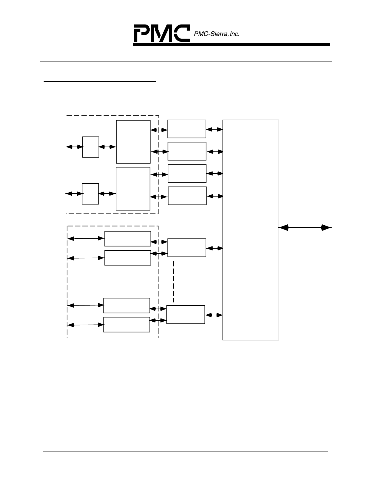
4 APPLICATION EXAMPLES
Figure 1 - High Density Channelized Port Card Application
#1 of 8
E1 C ha nne liz ed
E3 Interface
PM6388-RI
EOCTL
LIU
LIU
E13 Mux
E13 Mux
AND / O R
PM4314-RI
QDSX
PM4314-RI
QDSX
Channelized
And/Or Unchannelized E1
Inte r f a c e s
PM4314-RI
QDSX
PM4314-RI
QDSX
PM6388-RI
EOCTL
PM6388-RI
EOCTL
PM4388-RI
EOCTL
#4 of 8
PM6388-R I
EOCTL
#5 of 8
PM6388-RI
EOCTL
#8 of 8
PM7364
FREEDM (s)
Channelized
/Unchannelized
HDLC
Processor(s)
Packet Router Core
or
Packet Switch Core
PROPRIETARY and CONFIDENTIAL to PMC-Sierra Inc. and for its customers’ internal use 7
Page 27
PM6388 EOCTL
A
A
A
A
A
r
A
A
r
DATA SHEET
PMC-1971019 ISSUE 6 OCTAL E1 FRAMER
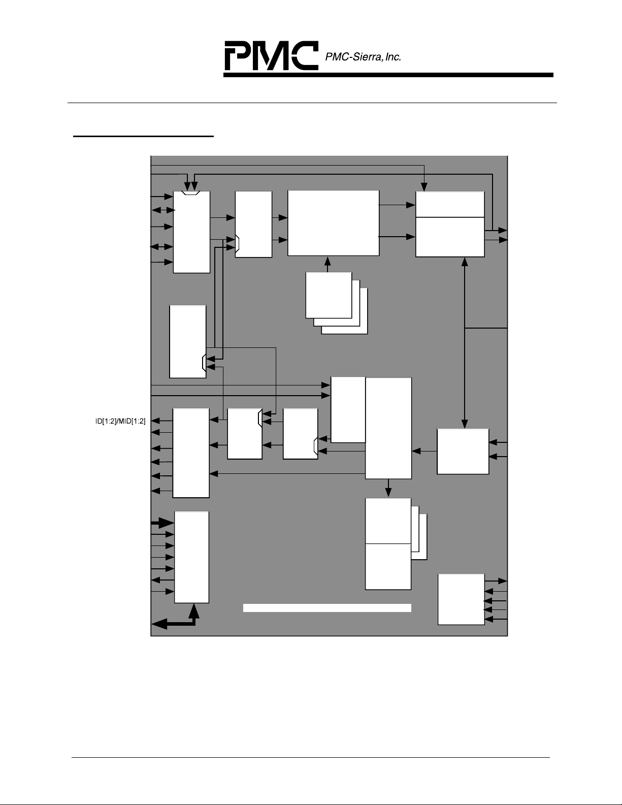
5 BLOCK DIAGRAM
CTCLK*
CECLK/MCECLK*
CEFP/MCEFP*
ESIG[1:2]/ECLK[1:2]/
EFP[1:2]/MESIG[1;2]
ED[1:2]/MED[1:2]
ESIG[3:8]/
ECLK[3:8]/
EFP[3:8]
ED[3:8]
BTIF
Backplane
Egress
Interface
PRGD
Pattern
Generator/
Detector
TPSC
Per-
Channel
Controller
TRANSMITTER
TRAN
BasicTransmitter:
Frame Generation,
larm Insertion,
Signaling Ins ertio n,
Trunk Conditioning
TDPR[2:0]
HDLC
Transmitter
TOPS
Timing Options
TJAT
Digital Jitter
ttenuato
TLCLK[1:8]
TLD[1:8]
XCLK*
CICLK/MCICLK*
CIFP/MCIFP*
ICLK[1:2]/ISIG[1:2]/
MISIG[1:2]
IFP[1:2]/MIFP[1:2]
ID[3:8]
ICLK[3:8]/
ISIG[3:8]
IFP[3:8]
[10:0]*
RDB*
WRB*
CSB*
LE*
INTB*
RSTB*
D[7:0]*
BRIF
Ingress
Backplane
Interface
MPIF
Micro-
Processor
Interface
RECEIVER
ELST
Elastic
SIGX
RPSC
Per-
Channel
Controller
* These signals are shared between all eight framers.
Signaling
Extractor
Store
ELST
Elastic
Store
Framer:
lignment,
Extraction
RDLC[2:0]
Performance
Counters
FRMR
Frame
larm
HDLC
Receiver
PMON
Monitor
RJAT
Digital Jitter
ttenuato
JTAG
Test Access
Port
RLCLK[1:8]
RLD[1:8]
TDO
TDI
TCLK
TMS
TRSTB
PROPRIETARY and CONFIDENTIAL to PMC-Sierra Inc. and for its customers’ internal use 8
Page 28

PM6388 EOCTL
DATA SHEET
PMC-1971019 ISSUE 6 OCTAL E1 FRAMER
6 DESCRIPTION
The PM6388 Octal E1 Framer (EOCTL) is a feature-rich device for use in systems
carrying data (frame relay, Point to Point Protocol, or other protocols) or voice over
E1 facilities. Each of the framers and transmitters is independently software
configurable, allowing feature selection without changes to external wiring.
On the receive side, each of eight independent framers can be configured to frame
to a basic G.704 2048 kbit/s signal as well as finding the signaling multiframe
alignment signal and the CRC multiframe alignment:. Framing can also be
bypassed (unframed mode). The EOCTL detects and indicates the presence
various alarm conditions such as loss of frame-alignment, loss of signaling
multiframe alignment, loss of CRC multiframe alignment, reception of remote alarm
indication signals, remote multiframe alarm signals, alarm indication signal (AIS),
and timeslot 16 alarm indication signal. The EOCTL integrates red and IS alarms as
per industry specifications. Performance monitoring with accumulation of CRC-4
errors, far-end block errors, framing bit errors, and out-of-frame events is provided.
The EOCTL also detects and terminates HDLC messages on TS16, the Sa National
bits, and/or on any arbitrary timeslot. Each HDLC link is terminated in a 128 byte
FIFO.
An elastic store that optionally supports slip buffering and adaptation to backplane
timing is provided, as is a signaling extractor that supports signaling debounce,
signaling freezing and interrupt on signaling state change on a per-channel basis.
The EOCTL also supports idle code substitution and detection, digital milliwatt code
insertion, data extraction, trunk conditioning, data inversion, and pattern generation
or detection on a per-channel basis.
On the transmit side, the EOCTL generates framing for a G.704 2048 kbit/s E1
signal. Framing can be optionally disabled. The signaling multiframe alignment
structure and the CRC multiframe structure may be optionally inserted. The EOCTL
supports signaling insertion, idle code substitution, data insertion, line loopback,
data inversion, and test pattern generation or detection on a per-channel basis.
Up to 3 HDLC links can be supported by the each octant of the EOCTL. Datalink
messages can be transmitted on TS16, the Sa National bits, and on an arbitrary
channel timeslot at the same time. The datalink messages may also be configured
to operate on 3 arbitrary channel timeslots.
The EOCTL can generate a low jitter transmit clock from a variety of clock
references, and also provides jitter attenuation in the receive path.
PROPRIETARY and CONFIDENTIAL to PMC-Sierra Inc. and for its customers’ internal use 9
Page 29

PM6388 EOCTL
DATA SHEET
PMC-1971019 ISSUE 6 OCTAL E1 FRAMER
The EOCTL provides a parallel microprocessor interface for controlling the operation
of the EOCTL device. Serial PCM interfaces allow 2048 kbit/s ingress/egress
system interfaces to be directly supported.
The EOCTL also supports an alternate backplane interface where up to 4 links can
be byte-multiplexed onto one of two 8.192 Mbit/s buses. A link can be placed on
either bus. Slots which are not occupied by a link from the EOCTL device can be
used by other devices attached to the bus. This bus protocol is consistent with that
defined in the Mitel ST®, A T&T CHI® and MVIP PCM standards.
It should be noted that the EOCTL device operates on unipolar data only: HDB3
encoding and line code violation monitoring, if required, must be processed by the
E1 LIU.
PROPRIETARY and CONFIDENTIAL to PMC-Sierra Inc. and for its customers’ internal use 10
Page 30
PM6388 EOCTL
DATA SHEET
PMC-1971019 ISSUE 6 OCTAL E1 FRAMER
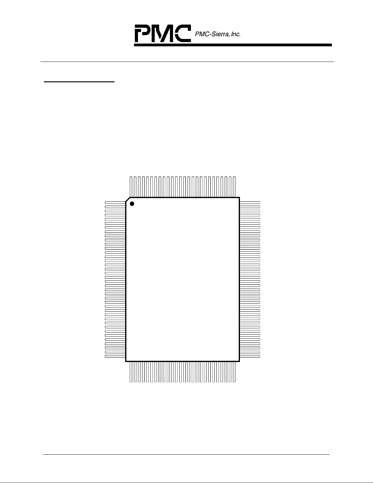
7 PIN DIAGRAM
The EOCTL is packaged in a 128-pin plastic QFP package having a body size of
14mm by 20mm and a pin pitch of 0.5 mm.
]
]
1
2
[
[
G
G
I
I
S
S
E
PIN 128
E
M
M
/
K
L
K
P
L
C
F
E
C
P
I
E
C
F
C
I
C
M
C
/
M
M
/
]
/
B
K
K
M
K
/
3
L
P
T
S
M
T
L
I
S
K
C
O
D
T
R
C
D
T
T
T
C
T
[
K
L
P
F
C
E
C
L
D
C
F
E
I
I
L
C
C
C
P
X
C
/
P
P
F
F
E
E
/
/
]
]
K
K
1
2
L
L
[
[
C
C
D
D
]
E
E
E
E
/
3
/
[
D
H
P
]
M
3
M
G
G
/
[
I
/
I
D
D
S
S
D
E
E
E
E
E
]
]
3
[
P
F
E
/
K
L
C
E
/
]
4
G
[
I
D
S
E
E
]
4
5
[
[
P
P
F
F
E
E
/
/
K
K
L
L
C
C
]
]
E
E
4
/
/
]
]
5
[
[
A
L
P
6
5
G
G
A
[
[
I
I
H
D
D
S
S
P
E
E
E
E
PIN 103
PIN 1
RLD[1]
RLCLK[1]
RLD[2]
RLCLK[2]
RLD[3]
RLCLK[3]
RLD[4]
RLCLK[4]
TLD[1]
TLCLK[1]
TLD[2]
TLCLK[2]
TLD[3]
TLCLK[3]
TLD[4]
TLCLK[4]
BIAS
PHA[0]
PLA[0]
PHD[0]
PLD[0]
TLD[5]
TLCLK[5]
TLD[6]
TLCLK[6]
TLD[7]
TLCLK[7]
TLD[8]
TLCLK[8]
PLA[1]
RLD[5]
RLCLK[5]
RLD[6]
RLCLK[6]
RLD[7]
RLCLK[7]
RLD[8]
RLCLK[8]
PIN 38
Index P in
PM6388
EOCTL
Top
View
PIN 102
ESIG/ECLK/EFP[6]
ED[7]
ESIG/ECLK/EFP[7]
ED[8]
ESIG/ECLK/EFP[8]
ID/M ID [1]
ICLK/ISIG /MISIG[ 1 ]
IFP/MIFP[1]
ID/M ID [2]
PLA[4]
PHA[3]
ICLK/ISIG /MISIG[ 2 ]
IFP/MIFP[2]
ID[3]
ICLK/ISIG [3]
IFP[3]
PLD[2]
PHD[2]
ID[4]
ICLK/ISIG [4]
IFP[4]
ID[5]
ICLK/ISIG [5]
IFP[5]
ID[6]
ICLK/ISIG [6]
IFP[6]
PLA[3]
PHA[2]
ID[7]
ICLK/ISIG [7]
IFP[7]
ID[8]
ICLK/ISIG [8]
IFP[8]
RDB
WRB
CSB
PIN 65
D[3]
D[4]
D[2]
D[1]
D[0]
INTB
RSTB
PHA[1]
D[7]
D[6]
PLA[2]
D[5]
PHD[1]
ALE
PLD[1]
A[4]
A[3]
A[2]
A[0]
A[1]
A[8]
A[7]
A[10]
A[9]
A[5]
A[6]
PIN 39 PIN 64
PROPRIETARY and CONFIDENTIAL to PMC-Sierra Inc. and for its customers’ internal use 11
Page 31

PM6388 EOCTL
DATA SHEET
PMC-1971019 ISSUE 6 OCTAL E1 FRAMER
8 PIN DESCRIPTION
Pin Pin
Name Type No. Function
RLD[1]
RLD[2]
RLD[3]
RLD[4]
RLD[5]
RLD[6]
RLD[7]
RLD[8]
RLCLK[1]
RLCLK[2]
RLCLK[3]
RLCLK[4]
RLCLK[5]
RLCLK[6]
RLCLK[7]
RLCLK[8]
Input 1
31
33
35
37
Input 2
32
34
36
38
Receive Line Data (RLD[1:8]). RLD[1:8] contain the
3
receive stream from each of the eight E1 line
5
interface units, or from a higher order demultiplex
7
interface. These inputs are sampled on the active
edge of the corresponding RLCLK[1:8].
Receive Line Clocks (RLCLK[1:8]). Each input is
4
an externally recovered 2.048 MHz line clock that
6
samples the RLD[x] inputs on its active edge.
8
RLCLK[x] may be a gapped clock subject to the
timing constraints in the AC Timing section of this
datasheet.
PROPRIETARY and CONFIDENTIAL to PMC-Sierra Inc. and for its customers’ internal use 12
Page 32

PM6388 EOCTL
DATA SHEET
PMC-1971019 ISSUE 6 OCTAL E1 FRAMER
ICLK[1]
ICLK[2]
ICLK[3]
ICLK[4]
ICLK[5]
ICLK[6]
ICLK[7]
ICLK[8]/
ISIG[1]
ISIG[2]
ISIG[3]
ISIG[4]
ISIG[5]
ISIG[6]
ISIG[7]
ISIG[8]
Output 96
91
88
83
80
77
72
69
Ingress Clocks (ICLK[1:8]). The Ingress Clocks are
active when the external signaling interface is
disabled. Each ingress clock is a smoothed (jitter
attenuated) version of the associated receive line
clock (RLCLK[x]). When the Clock Master: NxTS
mode is active, ICLK[x] is a gapped version of the
smoothed RLCLK[x]. When Clock Slave: ICLK
Reference mode is active, ICLK[x] may optionally be
the smoothed RLCLK[x], or the smoothed RLCLK[x]
divided by 256. When Clock Master: Full E1 mode is
active, IFP[x] and ID[x] are updated on the active
edge of ICLK[x]. When the Clock Master: NxTS
mode is active, ID[x] is updated on the active edge of
ICLK[x].
Ingress Signaling (ISIG[1:8]). When the Clock
Slave: External Signaling mode is enabled, each
ISIG[x] contains the extracted signaling bits for each
channel in the frame, repeated for the entire signaling
multiframe. Each channel’s signaling bits are valid in
bit locations 5,6,7,8 of the channel and are channelaligned with the ID[x] data stream. ISIG[x] is updated
on the active edge of the common ingress clock,
CICLK
MISIG[1]
MISIG[2]
Multiplexed Ingress Signaling (MISIG[1:2): When
96
the Multiplexed bus structure is enabled, MISIG[1:2]
91
carry the signaling data for the selected links.
MISIG[1:2] are updated on the active edge of
MCICLK.
PROPRIETARY and CONFIDENTIAL to PMC-Sierra Inc. and for its customers’ internal use 13
Page 33

PM6388 EOCTL
DATA SHEET
PMC-1971019 ISSUE 6 OCTAL E1 FRAMER
IFP[1]
IFP[2]
IFP[3]
IFP[4]
IFP[5]
IFP[6]
IFP[7]
IFP[8]
Output 95
90
87
82
79
76
71
68
Ingress Frame Pulse (IFP[1:8]). The IFP[x] outputs
are intended as timing references.
IFP[x] indicates the frame alignment or, optionally, the
signaling multiframe and/or the CRC multiframe
alignment of the ingress stream, ID[x]. When
configured for simple frame alignment, IFP[x] will
pulse high on the first bit of the each frame aligned to
ID[x]. When configured to indicate signaling
multiframe, IFP[x] will pulse high during the first bit of
the first frame of the signaling multiframe. When
configured to indicate CRC multiframe, IFP[x] will
pulse high during the first bit of the first frame of the
CRC multiframe. When configured to indicate both
the signaling and CRC multiframes, IFP[x] will go high
on the first bit of the first frame of the signaling
multiframe and low after the first bit of the first frame
of the CRC multiframe. Alternatively, IFP[x] can be
configured as a referance frame pulse which will
indicate the first bit of the E1 frame irrespective of bit
or timeslot offset.
When the Clock Master ingress modes are active,:
IFP[x] is updated on the active edge of the associated
ICLK[x]. When the Clock Slave ingress modes are
active, IFP[x] is updated on the active edge of CICLK.
MIFP[1:2]
95
Multiplexed Ingress Frame Pulse (MIFP[1:2]).
90
When configured for the Multiplexed bus structure,
MIFP[1:2] will show the frame alignment of the data
given on the MID[1:2] multiplexed data stream. The
frame alignment signal for each link can behave the
same as IFP[x], or either MIFP can be configured as
a reference frame pulse indicating bit 1 of the
Multiplexed frame.
MIFP[1:2] are updated on the active edge of MCICLK.
PROPRIETARY and CONFIDENTIAL to PMC-Sierra Inc. and for its customers’ internal use 14
Page 34

PM6388 EOCTL
DATA SHEET
PMC-1971019 ISSUE 6 OCTAL E1 FRAMER
ID[1]
ID[2]
ID[3]
ID[4]
ID[5]
ID[6]
ID[7]
ID[8]
MID[1]
MID[2]
CICLK
MCICLK
Output 97
94
89
84
81
78
73
70
97
94
Input 120
Ingress Data (ID[1:8]). Each ID[x] signal contains
the recovered data stream which may have been
passed through the elastic store.
When the Clock Slave ingress modes are active, the
ID[x] stream is aligned to the common ingress timing
and is updated on the active edge of CICLK.
When the Clock Master ingress modes are active,
ID[x] is aligned to the receive line timing and is
updated on the active edge of the associated ICLK[x].
Multiplexed Ingress Data (MID[1:2]). When
configured for the Multiplexed bus structure, MID[1:2]
contain the ingress data streams configured to be on
the two buses. MID[1:2] are updated on the active
edge of MCICLK.
Common Ingress Clock (CICLK). CICLK is a
2.048MHz clock with optional gapping for adaptation
to non-uniform backplane data streams. CICLK is
common to all eight framers. CIFP is sampled on the
active edge of CICLK. When the Clock Slave ingress
modes are active, ID[x], ISIG[x], and IFP[x] are
updated on the active edge of CICLK.
Multiplexed Common Ingress Clock (MCICLK).
When configured for the Multiplexed bus structure,
MCICLK drives the ingress multiplexed bus.
MCICLK is a 8.192 Mhz or 16.384 MHz clock.
PROPRIETARY and CONFIDENTIAL to PMC-Sierra Inc. and for its customers’ internal use 15
Page 35

PM6388 EOCTL
DATA SHEET
PMC-1971019 ISSUE 6 OCTAL E1 FRAMER
CIFP
MCIFP
ED[1]
ED[2]
ED[3]
ED[4]
ED[5]
ED[6]
ED[7]
ED[8]
Input 119
Input 115
113
111
109
105
103
101
99
Common Ingress Frame Pulse (CIFP). When the
elastic store is enabled (Clock Slave mode is active
on the ingress side), CIFP is used to frame align the
ingress data to the system frame alignment. CIFP is
common to all eight framers. When frame alignment
is required, a pulse at least 1 CICLK cycle wide must
be provided on CIFP a maximum of once every frame
(nominally 256 bit times).
CIFP is sampled on the active edge of CICLK.
Multiplexed Common-Ingress Frame Pulse
(MCIFP). When the Multiplexed bus structure is
enabled, CIFP is used to align the the bit-slots of the
multiplexed bus. The bit-slot where MCIFP is active
will become the first bit-slot of th e bus’ data stream.
MCIFP is sampled on the active edge of MCICLK.
Egress Data (ED[1:8]). The egress data streams to
be transmitted are input on these pins. When the
Clock Master: Full E1 mode is active, ED[x] is
sampled on the active edge of TLCLK[x]. When the
Clock Master: NxTS mode is active, ED[x] is sampled
on the active edge of ECLK[x]. When the Clock
Slave egress modes are active, ED[x] is sampled on
the active edge of CECLK
MED[1]
MED[2]
115
113
Multiplexed Bus Egress Data (MED[1:2). When
configured for the Multiplexed bus structure, MED[1:2]
are the egress data streams. Data for each link must
configured to originate from an 8-bit-wide slot within
one of the two MED data streams. MED[1:2] are
sampled on the active edge of MCECLK.
PROPRIETARY and CONFIDENTIAL to PMC-Sierra Inc. and for its customers’ internal use 16
Page 36

PM6388 EOCTL
DATA SHEET
PMC-1971019 ISSUE 6 OCTAL E1 FRAMER
ESIG[1]
ESIG[2]
ESIG[3]
ESIG[4]
ESIG[5]
ESIG[6]
ESIG[7]
ESIG[8]
EFP[1]
EFP[2]
EFP[3]
EFP[4]
EFP[5]
EFP[6]
EFP[7]
EFP[8]/
ECLK[1]
ECLK[2]
ECLK[3]
ECLK[4]
ECLK[5]
ECLK[6]
ECLK[7]
ECLK[8]
I/O 114
112
110
106
104
102
100
98
Egress Signaling (ESIG[1:8]). When the Clock
Slave: External Signaling mode is active, the
ESIG[8:1] inputs contain the signaling bits for each
channel in the transmit data frame, repeated for the
entire signaling multiframe. Each channel’s signaling
bits are in bit locations 5,6,7,8 of the channel and are
frame-aligned by the common egress frame pulse,
CEFP. ESIG[x] is sampled on the active edge of
CECLK.
Egress Frame Pulse (EFP[1:8]). When the Clock
Master: Full E1 or Clock Slave: EFP Enabled modes
are active, the EFP[1:8] outputs indicate the frame
alignment or the CRC and Signaling Multiframe
alignment of each of the eight framers. EFP[x] is
updated by the active edge of the TLCLK[x] output
(Clock Master), or CECLK input (Clock Slave).
Egress Clock (ECLK[1:8]). When the Clock Master:
NxTS mode is active, the ECLK[x] output is used to
sample the associated egress data (ED[x]). ECLK[x]
is a version of TLCLK[x] that is optionally gapped for
between 1 and 32 channel timeslots in the associated
ED[x] stream. ED[x] is sampled on the active edge of
the associated ECLK[x].
MESIG[1]
MESIG[2]
114
112
Multiplexed Bus Egress Signaling (MESIG[1:2]).
When the Multiplexed bus structure is enabled,
MESIG[1:2] carries the signaling data for the links
configured to be on the two buses. MESIG[1:2] is
sampled on the active edge of MCECLK.
PROPRIETARY and CONFIDENTIAL to PMC-Sierra Inc. and for its customers’ internal use 17
Page 37

PM6388 EOCTL
DATA SHEET
PMC-1971019 ISSUE 6 OCTAL E1 FRAMER
CTCLK Input 123
CECLK
Input 122
Common Transmit Clock (CTCLK). This input
signal is used to generate the TLCLK[x] clock signals.
Depending on the configuration of the EOCTL,
CTCLK may be a 16.384 MHz clock (so TLCLK[x] is
generated by dividing CTCLK by 8), or a line rate
clock (so TLCLK[x] is generated directly from CTCLK,
or from CTCLK after jitter attenuation), or a multiple of
8kHz (Nx8khz, where 1 ≤ Ν ≤ 256) so long as CTCLK
is jitter-free when divided down to 8kHz (in which
case TLCLK is derived by the DJAT PLL using
CTCLK as a reference).
The EOCTL may be configured to ignore the CTCLK
input and utilize CECLK or RLCLK[x] instead.
RLCLK[x] is automatically substituted for CTCLK if
line loopback is enabled.
Common Egress Clock (CECLK). The common
egress clock is used to time the egress interface
when Clock Slave mode is enabled in the egress
side. CECLK is nominally a 2.048MHz clock with
optional gapping for adaptation from non-uniform
system clocks. When the Clock Slave: EFP Enabled
mode is active, CEFP and ED[x] are sampled on the
active edge of CECLK, and EFP[x] is updated on the
active edge of CECLK. When the Clock Slave:
External Signaling mode is active, CEFP, ESIG[x] and
ED[x] are sampled on the active edge of CECLK.
MCECLK
Multiplexed Common Egress Clock (MCECLK).
When the Multiplexed bus structure is enabled,
MCECLK is a 8.192 MHz or 16.384 Mhz clock which
drives the two Multiplexed buses and samples the
data on MESIG[1:2], MED[1:2], and the alignment
signal on MCEFP.
PROPRIETARY and CONFIDENTIAL to PMC-Sierra Inc. and for its customers’ internal use 18
Page 38

PM6388 EOCTL
DATA SHEET
PMC-1971019 ISSUE 6 OCTAL E1 FRAMER
CEFP
MCEFP
TLCLK[1]
TLCLK[2]
TLCLK[3]
TLCLK[4]
TLCLK[5]
TLCLK[6]
TLCLK[7]
TLCLK[8]
Input 121
Output 10
12
14
16
23
25
27
29
Common Egress Frame Pulse (CEFP). CEFP may
be used to frame align the framers to the system
backplane. If frame alignment only is required, a
pulse at least 1 CECLK cycle wide must be provided
on CEFP every 256 bit times.
Multiplexed Common Egress Frame Pulse
(MCEFP). If the multiplexed bus structure is enabled,
MCEFP is used to align the bit-slots on the MED[1:2]
and MESIG[1:2] buses. The bit-slot where MCEFP is
active will become the first bit –slot of th e multiplexed
data streams. MCEFP is sampled on the active edge
of MCECLK.
Transmit Line Clock (TLCLK[1:8]). The TLD[x]
outputs are updated on the active edge of the
associated TLCLK[x]. When the Clock Master: Full
E1 mode is active, ED[1:8] is sampled on the active
edge of TLCLK[x] and EFP[1:8] is updated on the
active edge of TLCLK[x]. TLCLK[x] is a 2.048 MHz
clock that is adequately jitter and wander free in
absolute terms to permit an acceptable E1 signal to
be generated. Depending on the configuration of the
EOCTL, TLCLK[x] may be derived from CTCLK,
CECLK, or RLCLK[x], with or without jitter attenuation.
TLD[1]
TLD[2]
TLD[3]
TLD[4]
TLD[5]
TLD[6]
TLD[7]
TLD[8]
XCLK/
VCLK
Output 9
11
13
15
22
24
26
28
Input 117
Transmit Line Data (TLD[1:8]). TLD[1:8] contain the
transmit stream for each of the eight E1 line interface
units, or for the higher order multiplex interface.
These outputs are updated on the active edge of the
corresponding TLCLK[1:8].
Crystal Clock Input (XCLK). This signal provides
timing for many portions of the EOCTL. XCLK is
nominally a 49.152 MHz ± 50ppm, 50% duty cycle
clock.
Vector Clock (VCLK). The VCLK signal is used
during EOCTL production test to verify internal
functionality.
PROPRIETARY and CONFIDENTIAL to PMC-Sierra Inc. and for its customers’ internal use 19
Page 39

PM6388 EOCTL
DATA SHEET
PMC-1971019 ISSUE 6 OCTAL E1 FRAMER
INTB Output 40
CSB Input 65
D[0]
D[1]
D[2]
D[3]
D[4]
D[5]
D[6]
D[7]
I/O 41
42
43
44
45
46
47
48
RDB Input 67
Active low open-drain Interrupt signal (INTB). This
signal goes low when an unmasked interrupt event is
detected on any of the internal interrupt sources.
Note that INTB will remain low until a ll active,
unmasked interrupt sources are acknowledged at
their source.
Active low chip selec t (CSB). This signal must be
low to enable EOCTL register accesses. CSB must
go high at least once after a powerup to clear internal
test modes. If CSB is not used, then it should be tied
to an inverted version of RSTB, in which case, RDB
and WRB determine register accesses.
Bidirectional data bus (D[7:0]). This bus is used
during EOCTL read and write accesses.
Active low read enable (RDB). This signal is pulsed
low to enable a EOCTL register read access. The
EOCTL drives the D[7:0] bus with the contents of the
addressed register while RDB and CSB are both low.
WRB Input 66
Active low write strobe (WRB). This signal is pulsed
low to enable a EOCTL register write access. The
D[7:0] bus contents are clocked into the addressed
normal mode register on the rising edge of WRB
while CSB is low.
ALE Input 53
Address latch enable (ALE). This signal latches the
address bus contents, A[10:0], when low, allowing the
EOCTL to be interfaced to a multiplexed address/data
bus. When ALE is high, the address latches are
transparent. ALE has an integral pull-up.
RSTB Input 39
Active low reset (RSTB). This signal is set low to
asynchronously reset the EOCTL. RSTB is a
Schmitt-trigger input with integral pull-up. When
resetting the device, RSTB must be asserted for a
minimum of 100 ns to ensure that the EOCTL is
completely reset.
PROPRIETARY and CONFIDENTIAL to PMC-Sierra Inc. and for its customers’ internal use 20
Page 40

PM6388 EOCTL
DATA SHEET
PMC-1971019 ISSUE 6 OCTAL E1 FRAMER
A[0]
A[1]
A[2]
A[3]
A[4]
A[5]
A[6]
A[7]
A[8]
A[9]
A[10]
Input 54
55
56
57
58
59
60
61
62
63
64
TCK Input 126
TMS Input 128
TDI Input 127
Address bus (A[10:0]). This bus selects specific
registers during EOCTL register accesses.
Test Clock (TCK).The test clock (TCK) signal
provides timing for test operations that can be carried
out using the IEEE P1149.1 test access port.
Test Mode Select (TMS). The test mode select
(TMS) signal controls the test operations that can be
carried out using the IEEE P1149.1 test access port.
TMS is sampled on the rising edge of TCK. TMS has
an integral pull up resistor.
Test Input (TDI).The test data input (TDI) signal
carries test data into the EOCTL via the IEEE
P1149.1 test access port. TDI is sampled on the
rising edge of TCK. TDI has an integral pull up
resistor.
TDO Tristate 124
Test Output (TDO).The test data output (TDO) signal
carries test data out of the EOCTL via the IEEE
P1149.1 test access port. TDO is updated on the
falling edge of TCK. TDO is a tristate outpu t which is
tristated except when scanning of data is in progress.
TRSTB Input 125
Test Reset (TRSTB).The active low test reset
(TRSTB) signal provides an asynchronous EOCTL
test access port reset via the IEEE P1149.1 test
access port. TRSTB is a Schmitt triggered input with
an integral pull up resistor.
The JTAG TAP controller must be initialized when the
EOCTL is powered up. If the JTAG port is not used
TRSTB must be connected to the RSTB input or
grounded.
PROPRIETARY and CONFIDENTIAL to PMC-Sierra Inc. and for its customers’ internal use 21
Page 41

PM6388 EOCTL
DATA SHEET
PMC-1971019 ISSUE 6 OCTAL E1 FRAMER
BIAS Input 17
PHA[0]
PHA[1]
PHA[2]
PHA[3]
PHA[4]
PHD[0]
PHD[1]
PHD[2]
PHD[3]
PLA[0]
PLA[1]
PLA[2]
PLA[3]
PLA[4]
PLA[5]
Power 18
49
74
92
107
Power 20
51
85
116
Ground 19
30
50
75
93
108
+5V Bias (BIAS). The BIAS input is used to
implement 5V tolerance on the inputs. BIAS must be
connected to a well decoupled +5V rail if 5V tolerant
inputs are required. If 5V tolerant inputs are not
required, BIAS must be connected to a welldecoupled 3.3V DC supply together with the power
pins PHA[3:0] and PHD[3:0].
Pad ring power pins (PHA[4:0]). These pins must
be connected to a common, well decoupled +3.3V
DC supply together with the core power pins
PHD[3:0] .
Core power pins (PHD[3:0]). These pins must be
connected to a common, well decoupled +3.3V DC
supply together with the pad ring power pins
PHA[4:0].
Pad ring ground pins (PLA[5:0]). These pins must
be connected to a common ground together with the
core ground pins PLD[3:0].
PLD[0]
PLD[1]
PLD[2]
PLD[3]
Ground 21
52
86
118
Core ground pins (PLD[3:0]). These pins must be
connected to a common ground together with the pad
ring ground pins PLA[5:0].
Notes on Pin Description:
1. The PLA[5:0] and PLD[3:0] ground pins are not internally connected together.
Failure to connect these pins externally may cause malfunction or damage
the device. The PHA[4:0] and PHD[3:0] power pins are not internally
connected together. Failure to connect these pins externally may cause
malfunction or damage the device. These power supply connections must all
be utilized and must all connect to a common +3.3 V or ground rail, as
appropriate.
2. During power-up, and power-down the voltage on the BIAS pin must be kept
equal to or greater than the voltage on the PHA[4:0] and PHD[3:0] pins, to
avoid damage to the device.
PROPRIETARY and CONFIDENTIAL to PMC-Sierra Inc. and for its customers’ internal use 22
Page 42

PM6388 EOCTL
DATA SHEET
PMC-1971019 ISSUE 6 OCTAL E1 FRAMER
3. Inputs RSTB, TMS, TDI, and ALE have integral pull-up resistors.
4. All outputs have 2 mA drive capability except for the D[7:0] bidirectionals and
the TLCLK[8:1], ECLK[8:1], and ICLK[8:1] clock outputs which have 3 mA
drive capability.
5. All inputs and bidirectionals present minimum capacitive loading.
6. Certain inputs are described as being sampled by the “active edge” of a
particular clock. These inputs may be enabled to be sampled on either the
rising edge or the falling edge of that clock, depending on the software
configuration of the device.
.
PROPRIETARY and CONFIDENTIAL to PMC-Sierra Inc. and for its customers’ internal use 23
Page 43

PM6388 EOCTL
DATA SHEET
PMC-1971019 ISSUE 6 OCTAL E1 FRAMER
9 FUNCTIONAL DESCRIPTION
9.1 E1 Framer (E1-FRMR)
The E1 framing function is provided by the E1-FRMR block The E1-FRMR searches
for frame alignment, CRC multiframe alignment, and Channel Associated Signaling
(CAS) multiframe alignment in the incoming recovered PCM stream.
Once the E1-FRMR TSB has found frame, the incoming data is continuously
monitored for framing bit errors, CAS multiframe alignment pattern errors, CRC
multiframe alignment pattern errors, and CRC errors. The E1-FRMR also detects
and indicates loss of frame, loss of signaling multiframe, and loss of CRC
multiframe, based on user-selectable criteria. The reframe operation can be
initiated by software (via a register bit), by excessive CRC errors, or when CRC
multiframe alignment is not found within 400ms. The E1-FRMR also identifies the
position of TS 0, TS 16, the FAS, the signaling multiframe alignment signal, and the
CRC multiframe alignment signal.
The E1-FRMR extracts TS 16 as a data link and provides a separate serial stream
output timed to a 64 kbit/s data link clock. The E1-FRMR also extracts the contents
of the International bits (from both the FAS frames and the NFAS frames), the
National bits, and the Extra bits (from TS 16 of frame 0 of the signaling multiframe),
and stores them in microprocessor-accessible registers, updated every NFAS frame
(for the International and National bits) and every signaling multiframe (for the Extra
bits). The E1-FRMR also extracts sub-multiframe aligned 4 bit codewords from
each of the National bit positions Sa4 to Sa8, and stores them in microprocessoraccessible registers that are updated every CRC sub-multiframe.
The E1-FRMR identifies the raw bit values for Remote Alarm (bit 3 in TS 0 of NFAS
frames) and Remote Signaling Multiframe Alarm (bit 6 of TS 16 of frame 0 of the
signaling multiframe) via microprocessor-accessible registers. Outputs are provided
to indicate the “debounced” Remote Alarm and Remote Signaling Multiframe Alarm
is present when the corresponding bit has been a logic 1 for 2 or 3 consecutive
occurrences. Detection of AIS and TS 16 AIS are indicated; AIS is also integrated
and an AIS Alarm is indicated if the AIS condition has persisted for at least 100 ms.
The out of frame (OOF=1) condition is also integrated, indicating a RED Alarm if the
OOF condition has persisted for at least 100 ms.
An interrupt output is provided to signal a change in the state of any status output
(OOF, OOSMF, OOCMF, AIS, or RED), and to signal when any event output (RRA,
RRMA, AISD, T16AISD, COFA, FER, SMFER, CMFER, CRCE, or FEBE) has
occurred. As well, interrupts may be generated every frame, CRC sub-multiframe,
CRC multiframe or signaling multifram e.
PROPRIETARY and CONFIDENTIAL to PMC-Sierra Inc. and for its customers’ internal use 24
Page 44

PM6388 EOCTL
DATA SHEET
PMC-1971019 ISSUE 6 OCTAL E1 FRAMER
Basic Frame Alignment Procedure
The E1-FRMR searches for basic frame alignment using the algorithm defined in
ITU-T Recommendation G.706 4.1.2 and 4.2.
The algorithm finds frame alignment by using the following sequence:
1. Search for the presence of the correct 7-bit FAS (‘0011011’);
2. Check that the FAS is absent in the following frame by verifying that bit 2 of the
assumed non-frame alignment sequence (NFAS) TS 0 byte is a logic 1;
3. Check that the correct 7-bit FAS is present in the assumed TS 0 byte of the next
frame.
If either of the conditions in steps 2 or 3 are not met, a new search for frame
alignment is initiated in the bit immediately following the second 7-bit FAS sequence
check. This “hold-off” is done to ensure that new frame alignment searches are
done in the next bit position, modulo 512. This facilitates the discovery of the
correct frame alignment, even in the presence of fixed timeslot data imitating FASs.
These algorithms provide robust framing operation even in the presence of random
bit errors: framing with algorithm #1 or #2 provides a 99.98% probability of finding
frame alignment within 1 ms in the presence of 10-3 bit error rate and no mimic
patterns.
Once frame alignment is found, the block sets the OOF indication low, indicates a
change of frame alignment (if it occurred), and monitors the frame alignment signal,
indicating errors occurring in the 7-bit FAS pattern and in bit 2 of NFAS frames, and
indicating the debounced value of the Remote Alarm bit (bit 3 of NFAS frames).
Using debounce, the Remote Alarm bit has <0.00001% probability of being falsely
-3
indicated in the presence of a 10
bit error rate. The block declares loss of frame
alignment if 3 consecutive FASs have been received in error or, additionally, if bit 2
of NFAS frames has been in error for 3 consecutive occasions. In the presence of a
random 10-3 bit error rate the frame loss criteria provides a mean time to falsely lose
frame alignment of >12 minutes.
The E1-FRMR can be forced to initiate a frame search at any time when any of the
following conditions are met:
- the software re-frame bit in the E1-FRMR Frame Alignment Options Register
goes to logic 1;
- the EXREFR input signal goes high;
- the CRC Frame Find Block is unable to find CRC multiframe alignment; or
- the CRC Frame Find Block a ccumulates excessive CRC evaluation errors (≥ 915
CRC errors in 1 second) and is enabled to force a re-frame.
PROPRIETARY and CONFIDENTIAL to PMC-Sierra Inc. and for its customers’ internal use 25
Page 45

PM6388 EOCTL
DATA SHEET
PMC-1971019 ISSUE 6 OCTAL E1 FRAMER
CRC Multiframe Find Procedure
The E1-FRMR searches for CRC multiframe alignment by observing whether the
International bits (bit 1 of TS 0) of NFAS frames fo llow the CRC multiframe
alignment pattern. Multiframe alignment is d eclared if at least two valid CRC
multiframe alignment signals are observed within 8 ms, with the time separating two
alignment signals being a multiple of 2 ms
Once CRC multiframe alignment is found, the block sets the OOCMF indication low,
and monitors the multiframe alignment signal, indicating errors occurring in the 6-bit
pattern, and indicating the value of the FEBE bits (bit 1 of frames 13 and 15 of the
multiframe). The block declares loss of CRC multiframe align ment if four
consecutive CRC multiframe alignment signals have been received in error, or if
frame alignment has been lost.
Under the CRC-to-non-CRC interworking algorithm, if the E1-FRMR can achieve
basic frame alignment with respect to the incoming data stream, but is unable to
achieve CRC-4 multiframe alignment within the subsequent 400ms, the distant end
is assumed is assumed to be a non CRC-4 interface. The details of this algorthm
are outlined in the state diagram below:
PROPRIETARY and CONFIDENTIAL to PMC-Sierra Inc. and for its customers’ internal use 26
Page 46

PM6388 EOCTL
(Op
g)
DATA SHEET
PMC-1971019 ISSUE 6 OCTAL E1 FRAMER
Figure 2 - E1-FRMR Framing Algorithm
Ou t of Frame
FAS_Find_1
FAS
found
NFAS_Find
NFAS
found
next fr ame
FAS_Find_2
3 consecutiv e FA S or NFAS
errors; manual re frame; or
excessiv e C RC er rors
NFAS
not found
next fr ame
FAS
not fo und
next fr ame
FAS_Find_1_Par
FAS
found
NFAS_Find_Par
NFAS
found
next fr ame
FAS_Find_2_Par
NFAS
not found
nex t fr ame
FAS
not found
next fr ame
FAS
found
next fr ame
CRCMFA
CRC to CR C
Interworking
Start 400 m s tim e r
and 8m s timer
BFA
8ms ex pire
8m s ex pire and
NOT(400ms expire)
Reset BFA to
most recently
found alignm e nt
CRCMFA_Par
tional settin
FAS
found
next fr ame
BFA_Par
CRCMFA_P ar
CRC to non-CRC
Interworking
Start 8ms timer
400ms
expire
PROPRIETARY and CONFIDENTIAL to PMC-Sierra Inc. and for its customers’ internal use 27
Page 47

PM6388 EOCTL
DATA SHEET
PMC-1971019 ISSUE 6 OCTAL E1 FRAMER
Table 1 - E1-FRMR CRC Frame Find State Machine Outputs
State OOF OOOF
FAS_Find_1 1 0
NFAS_Find 1 0
FAS_Find_2 1 0
BFA 0 0
CRC to CRC Interworking 0 0
FAS_Find_1_Par 0 1
NFAS_Find_Par 0 1
FAS_Find_2_Par 0 1
BFA_Par 0 0
CRC to non-CRC Interworking 0 0
From an out of sync state, the E1-FRMR attempts to find basic frame alignment in
accordance with the FAS/NFAS/FAS G.706 procedure outlined in the section above.
Upon achieving basic frame alignment, a 400ms timer is started, as well as an 8ms
timer. If two CRC multiframe alignment signals separated by a multiple of 2ms is
observed before the 8ms timer has expired, CRC mulitframe alignmen t is declared.
If the 8ms timer expires without achieving multiframe alignment, a new offline search
for basic frame alignment is initiated. This search is performed in accordance with
the Basic Frame alignment procedure outlined above. However, this search does
not immediately change the actual basic frame alignment of the system. (i.e. data
continues to be processed in accordance with the first basic frame alignment found
after an out of sync state while this frame alignment search occurs as a parallel
operation.)
When a new basic frame alignment is found by this offline search, the 8ms timer is
restarted. If two CRC multiframe alignment signals separated by a multiple of 2ms is
observed before the 8ms timer has expired, CRC m ulitframe alignment is declared
and the basic frame alignment is set accordingly. (i.e. The basic frame alignment is
set to correspond to the frame alignment found by the parallel offline search, which
PROPRIETARY and CONFIDENTIAL to PMC-Sierra Inc. and for its customers’ internal use 28
Page 48

PM6388 EOCTL
DATA SHEET
PMC-1971019 ISSUE 6 OCTAL E1 FRAMER
is also the basic frame alignment corresponding to the newly found CRC multiframe
alignment.)
Subsequent expirations of the 8ms timer will reinitiate a new search for basic frame
alignment. If, however, the 400ms timer expires at any time during this procedure,
the E1-FRMR stops searching for CRC multiframe alignment and declares CRC to
non CRC interworking. From this mode, the FRMR may either halt searching for
CRC multiframe altogether, or may continue searching for CRC multif rame
alignment using the established basic frame alignment. In either case, no further
adjustments are made to the basic frame alignment, and no offline searches for
basic frame alignment occur once CRC to non-CRC interworking is declared: it is
assumed that the established basic frame alignment at this point is correct.
CRC Checking and AIS Detection
The E1-FRMR computes the 4-bit CRC checksum for each incoming sub-multiframe
and compares this 4-bit result to the received CRC remainder bits in the subsequent
sub-multiframe. If a mismatch occurs, the E1-FRMR can initiate an interrupt. The
E1-FRMR also accumulates CRC errors over 1 second intervals, monitoring for
excessive CRC errors and optionally, initiatiating a frame search when ≥915 CRC
errors occur in 1 second. The number of CRC errors accumulated during the
previous second is available by reading the CRC Error Counter Registers.
The E1-FMR also detects the occurrence of an unframed all-ones receive data
stream, indicating the AIS by setting the AISD output high when less than 3 zero bits
are received in 512 consecutive bits or in each of 2 consecutive periods of 512 bits;
the AISD output is reset low when 3 or more zeros in the data stream are observed
in 512 consecutive bits or in each of 2 consecutive periods of 512 bits. Finding
frame alignment will also cause the AISD indication to be deasserted.
Signaling Frame Find Block
The E1-FRMR searches for signaling multiframe alignment using the following
G.732 compliant algorithm: signaling mulitframe alignment is declared when nonzero bits 1-4 of TS 16 are observed to precede a TS 16 containing the correct
alignment pattern.
Once signaling multiframe alignment has been found, the block sets the OOSMF
indication to logic 0, and monitors the signaling multiframe alignment signal,
indicating errors occurring in the 4-bit pattern, and indicating the debounced value of
the Remote Signaling Multiframe Alarm bit (bit 6 of TS 16 of frame 0 of the
multiframe). Using debounce, the Remote Signaling Multiframe Alarm bit has <
-3
0.00001% probability of being falsely indicated in the presence of a 10
bit error
rate.
PROPRIETARY and CONFIDENTIAL to PMC-Sierra Inc. and for its customers’ internal use 29
Page 49

PM6388 EOCTL
DATA SHEET
PMC-1971019 ISSUE 6 OCTAL E1 FRAMER
The block declares loss of signaling multiframe alignment if two consecutive
signaling multiframe alignment signals have been received in error, or additionally, if
all the bits in TS16 are logic 0 for 1 or 2 (selectable) signaling multiframes. Loss of
signaling multiframe alignment is also declared if basic frame alignment has been
lost.
National Bits Extracti on
The E1-FRMR extracts and assembles the sub-multiframe aligned National bit
codewords Sa4[1:4] to Sa8[1:4]. The corresponding register values are updated
upon generation of the CRC sub-multiframe interrupt.
This block also detects the V5.2 link ID signal, which is defined as the event where 2
out of 3 Sa7 bits are logic 0. Upon reception of this Link ID signal, the V52LINK
output is asserted. This signal is cleared when 2 out of 3 Sa7 bits are a logic one.
Alarm Integration
The E1-FRMR monitors the OOF and the AISD indications, verifying that each
condition has persisted for 104 ms (±6 ms) before indicating the alarm condition.
The alarm is removed when the condition has been absent for 104 ms (±6 ms).
The AIS Alarm algorithm accumulates the occurrences of AISD over a 4 ms interval
and indicates a valid AIS presence when 13 or more AISD indications have been
received. Each interval with a valid AIS presence indication increments an interval
counter which declares AIS Alarm when 25 valid intervals have been accumulated.
An interval with no valid AIS presence indication decrements the interval counter;
the AIS Alarm declaration is removed when the counter reaches 0. This algorithm
provides a 99.8% probability of declaring an AIS Alarm in the presence of a 10
-3
mean bit error rate.
The RED Alarm algorithm monitors occurrences of OOF over a 4 ms interval,
indicating a valid OOF interval when one or more OOF indications occurred during
the interval, and indicating a valid in frame (INF) interval when no OOF indication
occurred for the entire interval. Each interval with a valid OOF indication increments
an interval counter which declares RED Alarm when 25 valid intervals have been
accumulated. An interval with valid INF indication decrements the interval counter;
the RED Alarm declaration is removed when the counter reaches 0. This algorithm
biases OOF occurrences, leading to declaration of RED Alarm when intermittent
loss of frame alignment occurs.
9.2 Performance Monitor Counters (PMON)
The Performance Monitor Counters function is provided by the PMON block. The
block accumulates CRC error events, Frame Synchronization bit error events, and
PROPRIETARY and CONFIDENTIAL to PMC-Sierra Inc. and for its customers’ internal use 30
Page 50

PM6388 EOCTL
DATA SHEET
PMC-1971019 ISSUE 6 OCTAL E1 FRAMER
FEBE events with saturating counters over consecutive intervals as defined by the
period of the supplied transfer clock signal (typically 1 second). When the transfer
clock signal is applied, the PMON transfers the counter values into holding registers
and resets the counters to begin accumulating events for the interval. The counters
are reset in such a manner that error events occurring during the reset are not
missed. If the holding registers are not read between successive transfer clocks, an
OVERRUN register bit is asserted.
Generation of the transfer clock within the EOCTL is performed by writing to any
counter register location or by writing to the Global PMON Update register. The
holding register addresses are contiguous to facilitate faster polling operations.
9.3 Data Link Extractor (RXCE)
The data link extraction is provided by the RXCE block. The RXCE allows the
optional extraction of per-timeslot data links from the received data stream.
Three independent data links can be extracted from three different timeslots. Each
data link can be configured to extract its data from an entire timeslot or just from any
combination of bits of a timeslot. Also, each data link can be extracted from every
frame or from only even or only odd frames.
9.4 HDLC Receiver (RDLC)
The HDLC Receiver function is provided by the RDLC block. The RDLC is a
microprocessor peripheral used to receive HDLC frames. Three RDLC blocks are
provided for flexible extraction of standardized data links:
• Common Channel Signaling data link
• V5.1/V5.2 D-channel and C-channels.
• Sa-bit data link
The RDLC detects the change from flag characters to the first byte of data, removes
stuffed zeros on the incoming data stream, receives packet data, and calculates the
CRC-CCITT frame check sequence (FCS).
In the address matching mode, only those packets whose first data byte matches
one of two programmable bytes or the universal address (all ones) are stored in the
FIFO. The two least significant bits of the address comparison can be masked for
LAPD SAPI matching.
Received data is placed into a 128-byte FIFO buffer. An interrupt is generated when
a programmable number of bytes are stored in the FIFO buffer. Other sources of
interrupt are detection of the terminating flag sequence, abort sequence, or FIFO
buffer overrun.
PROPRIETARY and CONFIDENTIAL to PMC-Sierra Inc. and for its customers’ internal use 31
Page 51

PM6388 EOCTL
DATA SHEET
PMC-1971019 ISSUE 6 OCTAL E1 FRAMER
The Status Register contains bits which indicate the overrun or empty FIFO status,
the interrupt status, and the occurrence of first flag or end of message bytes written
into the FIFO. The Status Register also indicates the abort, flag, and end of
message status of the data just read from the FIFO. On end of message, the Status
Register indicates the FCS status and if the packet contained a non-integer number
of bytes.
9.5 Elastic Store (ELST)
The Elastic Store (ELST) synchronizes ingress frames to the common ingress clock
and frame pulse (CICLK and CIFP or MCICLK and MCIFP) in the Clock Slave
ingress modes. The frame data is buffered in a two frame circular data buffer. Input
data is written to the buffer using a write pointer and output data is read from the
buffer using a read pointer.
The elastic store can be bypassed to eliminate the 2 frame delay. In this
configuration (the Clock Master ingress modes), the elastic store is used to
synchronize the ingress frames to the transmit line clock (TLCLK[x]) so that perchannel loopbacks may be enabled. Per-channel loopbacks are only available
when the elastic store is bypassed, or when CECLK and CICLK are tied together
and CEFP and CIFP are tied together, and the CICLKRISE and CECLKFALL
register bits are either both logic 1 or both logic 0. CICLKRISE and CECLKFALL
are found in registers 3 and 4 of each octant, respectively. The elastic store cannot
be bypassed if the Multiplexed bus is enabled.
When the elastic store is being used, if the average frequency of the incoming data
is greater than the average frequency of the backplane clock, the write pointer will
catch up to the read pointer and the buffer will be filled. Under this condition a
controlled slip will occur when the read pointer crosses the next frame boundary.
The subsequent ingress frame is deleted.
If the average frequency of the incoming data is less than the average frequency of
the backplane clock, the read pointer will catch up to the write pointer and the buffer
will be empty. Under this condition a controlled slip will occur when the read pointer
crosses the next frame boundary. The previous ingress frame is repeated.
A slip operation is always performed on a frame boundary.
For payload conditioning, the ELST can be configured to insert a programmable idle
code into all channels when the FRMR is out of frame alignment
9.6 Signaling Extractor (SIGX)
The Signaling Extraction (SIGX) block provides signaling bit extraction from timeslot
16 of the ingress. When the external signaling interface is enabled, the SIGX
PROPRIETARY and CONFIDENTIAL to PMC-Sierra Inc. and for its customers’ internal use 32
Page 52

PM6388 EOCTL
DATA SHEET
PMC-1971019 ISSUE 6 OCTAL E1 FRAMER
serializes the bits into a serial stream (ISIG[x] or MISIG[x]) aligned to the
synchronized outgoing data stream (ID[x] or MID[x]). The signaling data stream
contains the A,B,C,D bits in the lower 4 channel bit locations (bits 5,6,7,8). The
SIGX also provides user control over signaling freezing and provides control over
signaling bit fixing and signaling debounce on a per-channel basis. The block
contains three multiframes worth of signal buffering to ensure that there is a greater
than 95% probability that the signaling bits are frozen in the correct state for a 50%
ones density out-of-frame condition. With signaling debounce enabled, the perchannel signaling state must be in the same state for 2 multiframes before
appearing on the serial output stream. The SIGX indicates the occurrence of a
change of signaling state for each channel via an interrupt and by a change of
signaling state bit for each channel.
9.7 Receive Per-Channel Serial Controller (RPSC)
The RPSC allows data and signaling trunk conditioning to be applied on the receive
E1 stream on a per-channel basis. It also allows per-channel control of data
inversion, the extraction of clock and data on ICLK[x] and ID[x] (when the Clock
Master: NxTS mode is active), and the detection or generation of pseudo-random or
repetitive patterns. The RPSC operates on the data after its passage through ELST,
so that data and signaling conditioning may overwrite the ELST idle code.
9.8 P attern Detector/Generator (PRGD)
The Pattern Generator/Detector (PRGD) block is a software programmable test
pattern generator, receiver, and analyzer. Patterns may be generated in either the
transmit or receive directions, and detected in the opposite direction. Two types of
ITU-T O.151 compliant test patterns are provided : pseudo-random and repetitive.
The PRGD can be programmed to generate any pseudo-random pattern with length
up to 232-1 bits or any user programmable bit pattern from 1 to 32 bits in length. In
addition, the PRGD can insert single bit errors or a bit error rate between 10-1 to 10
7
.
The PRGD can be programmed to check for the presence of the generated pseudorandom pattern. The PRGD can perform an auto synchronization to the expected
pattern, and generate interrupts on detection and loss of the specified pattern. The
PRGD can accumulate the total number of bits received and the total number of bit
errors in two saturating 32-bit counters. The counters accumulate over an interval
defined by writes to the Revision/Chip ID/Global PMON Update register (register
00CH), by writes to any PRGD accumulation register, or over a one-second interval
timed to the receive line clock, via the AUTOUPDATE feature in the Receive Line
Options register (000H, 080H, 100H, 180H, 200H, 280H, 300H, 380H). When an
accumulation is forced by either method, then the holding registers are updated, and
the counters reset to begin accumulating for the next interval. The counters are
reset in such a way that no events are missed. The data is then available in the
-
PROPRIETARY and CONFIDENTIAL to PMC-Sierra Inc. and for its customers’ internal use 33
Page 53

PM6388 EOCTL
DATA SHEET
PMC-1971019 ISSUE 6 OCTAL E1 FRAMER
holding registers until the next accumulation. In addition to the two counters, a
record of the 32 bits received immediately prior to the accumulation is available.
The PRGD may also be programmed to check for repetitive sequences. When
configured to detect a pattern of length N bits, the PRGD will load N bits from the
detected stream, and determine whether the received pattern repeats itself every N
subsequent bits. Should it fail to find such a pattern, it will continue loading and
checking until it finds a repetitive pattern. All the features (error counting, autosynchronization, etc.) available for pseudo-random sequences are also available for
repetitive sequences. Whenever a PRGD accumulation is forced, the PRGD stores
a snapshot of the 32 bits received immediately prior to the accumulation. This
snapshot may be examined in order to determine the exact nature of the repetitive
pattern received by PRGD.
9.9 E1 Transmitter (E1-TRAN)
The E1 Transmitter (TRAN) generates a 2048 kbit/s data stream according to ITU-T
recommendations, providing individual enables for frame generation, CRC
multiframe generation, and channel associated signaling (CAS) multiframe
generation.
In concert with Transmit Per-Channel Serial Controller (TPSC), the TRAN block
provides per-timeslot control of idle code substitution, data inversion, digital milliwatt
substitution, selection of the signaling source and CAS data. All timeslots can be
forced into a trunk conditioning state (idle code substitution and signaling
substitution) by use of the master trunk conditioning bit in the Configuration
Register.
Common Channel Signaling (CCS) is supported in timeslot 16 through the internal
HDLC Transmitter (TDPR). Support is provided for the transmission of AIS and
TS16 AIS, and the transmission of remote alarm (RAI) and remote multiframe alarm
signals.
The E1-TRAN supports insertion of 4-bit code words into the National Bits Sa4 to
Sa8 as specified in ETS 300-233. Alternatively, the National bits may individually
carry data links sourced from the internal HDLC controllers, or may be passed
transparently from the ED[x] input.
9.10 Transmit Per-Channel Serial Controller (TPSC)
The Transmit Per-DS0 Serial Controller allows data and signaling trunk conditioning
or idle code to be applied on the transmit E1 stream on a per-channel basis. It also
allows per-channel control of datainversion, per-channel loopback (from the ingress
stream), channel insertion, and the detection or generation of pseudo-random or
repetitive patterns.
PROPRIETARY and CONFIDENTIAL to PMC-Sierra Inc. and for its customers’ internal use 34
Page 54

PM6388 EOCTL
DATA SHEET
PMC-1971019 ISSUE 6 OCTAL E1 FRAMER
The TPSC interfaces directly to the TRAN block and provides serial streams for
signaling control, idle code data, digital milliwatt insertion, and egress data control.
9.11 Transmit Data link Inserter (TXCI)
The facility data link insertio n functions are provided by the TXCI block. The TXCI
allows the optional insertion of per-timeslot functions into the output data stream.
The TXCI works with the TDPR, PRGD, and TPSC blocks for per-timeslot insertion
of test patterns, data streams, and data link streams.
Three independent data links can be inserted into three different timeslots. Each
data link can be configured to insert its data into the entire timeslot or just into a
certain combination of bits of the timeslot. Also, each data link can be inserted into
every frame or into only even or only odd frames.
Depending on the settings of the per-channel TPSC functions, the TXCI also assists
in executing per-timeslot functions such as payload loopback and PRBS test pattern
insertion.
9.12 Facility Data Link Transmitter (TDPR)
The Facility Data Link Transmitter (TDPR) provides serial data for th e 3 possible
data links (TS16, National Bits, and 1 arbitrary timeslot, or 3 arbitrary timeslots).
The TDPR is used under microprocessor control to transmit HDLC data frames.
It performs all of the data serialization, CRC generation, zero-bit stuffing, as well
as flag, and abort sequence insertion. Upon completion of the message, a CRCCCITT frame check sequence (FCS) may be appended, followed by flags. If the
TDPR transmit data FIFO underflows, an abort sequence is automatically
transmitted.
When enabled, the TDPR continuously transmits the flag sequence (01111110)
until data is ready to be transmitted. Data bytes to be transmitted are written into
the Transmit Data Register. The TDPR performs a parallel-to-serial conversion
of each data byte before transmitting it.
The TDPR automatically begins transmission of data once at least one complete
packet is written into its FIFO. All complete packets of da ta will be tran smitted.
After the last data byte of a packet, the CRC word (if CRC insertion has been
enabled) and a flag, or just a flag (if CRC insertion has not been enabled) is
transmitted. The TDPR then returns to the transmission of flag characters until
the next packet is available for transmission. The TDPR will also force
transmission of the FIFO data once the FIFO depth has surpassed the
programmable upper limit threshold. Transmission commences regardless of
whether or not a packet has been completely written into the FIFO. The user
must be careful to avoid overfilling the FIFO. Underruns can only occur if the
PROPRIETARY and CONFIDENTIAL to PMC-Sierra Inc. and for its customers’ internal use 35
Page 55

PM6388 EOCTL
DATA SHEET
PMC-1971019 ISSUE 6 OCTAL E1 FRAMER
packet length is greater than the programmed upper limit threshold because, in
such a case, transmission will begin bef o re a complete packet is stored in the
FIFO. An interrupt can be generated once the FIFO depth has fallen below a
user configured lower threshold as an indicator for the user to write more data.
Interrupts can also be generated if the FIFO underflows while transmitting a
packet, when the FIFO is full, or if the FIFO is overrun.
If there are more than five consecutive ones in the raw transmit data or in the
CRC data, a zero is stuffed into the serial data output. This prevents the
unintentional transmission of flag or abort sequences.
Abort characters can be continuously transmitted at any time by setting a control
bit. During packet transmission, an underrun situation can occur if data is not
written to the TDPR Transmit Data register before the previous byte has been
depleted. In this case, an abort sequence is transmitted, and the controlling
processor is notified via the UDRI interrupt.
9.13 Receive and Transmit Digital Jitter Attenuator (RJAT, TJAT)
The Digital Jitter Attenuation function is provided by the DJAT blocks. Each framer in
the EOCTL contains two separate jitter attenuators, one between the receive line
data and the ingress interface (RJAT) and the other between the egress interface
and the transmit line data (TJAT). Each DJAT block receives jittered data and stores
the stream in a FIFO timed to the associated clock (either RLCLK[x] or CECLK). The
jitter attenuated data emerges from the FIFO timed to the jitter attenuated clock. In
the RJAT, the jitter attenuated clock (ICLK[x]) is referenced to RLCLK[x]. In the
TJAT, the jitter attenuated clock TLCLK[x] may be referenced to either CTCLK,
CECLK, or RLCLK[x].
Each jitter attenuator generates its output clock by adaptively dividing the 49.152
MHz XCLK signal according to the phase difference between the jitter attenuated
clock and the reference clock. Jitter fluctuations in the phase of the reference clock
are attenuated by the phase-locked loop within each DJAT so that the frequency of
the jitter attenuated clock is equal to the average frequency of the reference. Phase
fluctuations with a jitter frequency above 8.8 Hz are attenuated by 6 dB per octave
of jitter frequency. Wandering phase fluctuations with frequencies below 8.8 Hz are
tracked by the jitter attenuated clock. The jitter attenuated clock (ICLK[x] for the
RJAT and TLCLK[x] for the TJAT) is used to read data out of the FIFO.
If the FIFO read pointer comes within one bit of the write pointer, DJAT will track the
jitter of the input clock. This permits the phase jitter to pass through unattenuated,
inhibiting the loss of data.
PROPRIETARY and CONFIDENTIAL to PMC-Sierra Inc. and for its customers’ internal use 36
Page 56

PM6388 EOCTL
DATA SHEET
PMC-1971019 ISSUE 6 OCTAL E1 FRAMER
Jitter Characteristics
Each DJAT Block provides excellent jitter tolerance and jitter attenuation while
generating minimal residual jitter. It can accommodate up to 35 UIpp of input jitter
at jitter frequencies above 9 Hz. For jitter frequencies below 9 Hz, more correctly
called wander, the tolerance increases 20 dB per decade. In most applications the
each DJAT Block will limit jitter tolerance at lower jitter frequencies only. For high
frequency jitter, above 10 kHz for example, other factors such as clock and data
recovery circuitry may limit jitter tolerance and must be considered. For low
frequency wander, below 10 Hz for example, other factors such as slip buffer
hysteresis may limit wander tolerance and must be considered. The DJAT blocks
meet the low frequency jitter tolerance requirements ITU-T Recommendation G.823.
DJAT exhibits negligible jitter gain for jitter frequencies below 8.8 Hz, and attenuates
jitter at frequencies above 8.8 Hz by 20 dB per decade. In most applications the
DJAT Blocks will determine jitter attenuation for higher jitter frequencies only.
Wander, below 10 Hz for example, will essentially be passed unattenuated through
DJAT. Jitter, above 10 Hz for example, will be attenuated as specified, however,
outgoing jitter may be dominated by the generated residual jitter in cases where
incoming jitter is insignificant. This generated residual jitter is directly related to the
use of 24X (49.152 MHz) digital phase locked loop for transmit clock generation.
DJAT meets the jitter transfer requirements of ITU-T Recommendations G.737,
G.738, G.739, and G.742.
Jitter Tolerance
Jitter tolerance is the maximum input phase jitter at a given jitter frequency that a
device can accept without exceeding its linear operating range, or corrupting data.
For DJAT, the input jitter tolerance is 35 Unit Intervals peak-to-peak (UIpp) with a
worst case frequency offset of 308 Hz. It is 48 UIpp with no frequency offset. The
frequency offset is the difference between the frequency of XCLK divided by 24 and
that of the input data clock.
PROPRIETARY and CONFIDENTIAL to PMC-Sierra Inc. and for its customers’ internal use 37
Page 57

PM6388 EOCTL
DATA SHEET
PMC-1971019 ISSUE 6 OCTAL E1 FRAMER
Figure 3 - DJAT Jitter Tolerance
100
Jitter
40
10
DJAT
minimum
tolerance
35
Am plitude,
UI pp
1.5
1.0
ITU -T G.82 3
acceptable
unacceptable
Region
0.2
0.1
0.01
1
10
20
100 1k 10k
2.4k 18k
100k
Jitter Frequency, Hz
The accuracy of the XCLK frequency and that of the reference clock used to
generate the jitter attenuated clock have an effect on the minimum jitter tolerance.
Given that the DJAT PLL reference clock accuracy can be ±103 Hz from 2.048 MHz,
and that the XCLK input accuracy can be ±100 ppm from 49.152 MHz, the minimum
jitter tolerance for various differences between the frequency of PLL reference clock
and XCLK ÷ 24 are shown in Figure 4.
PROPRIETARY and CONFIDENTIAL to PMC-Sierra Inc. and for its customers’ internal use 38
Page 58

PM6388 EOCTL
DATA SHEET
PMC-1971019 ISSUE 6 OCTAL E1 FRAMER
Figure 4 - DJAT Minimum Jitter Tolerance vs. XCLK Accuracy
45
42.4
40
DJAT Minimum
Jitter To le ra nc e
UI pp
35
39
34.9
Max frequency
offset (PLL Ref
30
100 200 300
308
Hz
to XC LK )
XCLK A ccuracy
0 100
49
± ppm
Jitter Transfer
The output jitter for jitter frequencies from 0 to 8.8 Hz is no more than 0.1 dB greater
than the input jitter, excluding the residual jitter. Jitter frequencies above 8.8 Hz are
attenuated at a level of 6 dB per octave, as shown in Figure 5.
Figure 5 - DJAT Jitter Transfer
0
-10
DJAT
response
-20
Jitter G a in
(dB )
-30
G.737, G738,
G.739, G.742
max
Unacceptable
Region
-19.5
-40
-50
1
8.8
10
40
100 1k 10k
Jitter Frequency, Hz
PROPRIETARY and CONFIDENTIAL to PMC-Sierra Inc. and for its customers’ internal use 39
Page 59

PM6388 EOCTL
DATA SHEET
PMC-1971019 ISSUE 6 OCTAL E1 FRAMER
Frequency Range
In the non-attenuating mode, that is, when the FIFO is within one UI of overrunning
or under running, the tracking range is 1.963 to 2.133 MHz. The guaranteed linear
operating range for the jittered input clock is 2.048 MHz ± 103 Hz with worst case
jitter (42 UIpp) and maximum XCLK frequency offset (± 100 ppm). The nominal
range is 2.048 MHz ± 1278 Hz with no jitter or XCLK frequency offset.
9.14 Timing Options (TOPS)
The Timing Options block provides a means of selecting the source of the
internal input clock to the TJAT block, the reference clock for the TJAT digital
PLL, and the clock source used to derive the output TLCLK[x] signal.
9.15 Backplane Receive Interface (BRIF)
9.15.1 Non-Multiplexed Bus Ingress Modes
The Ingress Interface allows ingress data to be presented to a system using one of
four possible modes as selected by the ICLKSLV and ISIG_EN bits in the Receive
Backplane Configuration (Register 010H, 090H, 110H, 190H, 210H, 290H, 310H,
390H) and Ingress Interface Options (Register 001H, 081H, 101H, 181H, 201H,
281H, 301H, 381H) Registers respectively: Clock Master: Full E1, Clock Master :
NxTS, Clock Slave : ICLK Reference, or Clock Slave: External Signaling.
Figure 6 - Clock Master: Full E1.
FRMR
ID[1:8]
IFP[1:8]
ID[x], IFP[x]
Timed to ICLK[x]
ICLK[1:8]
BRIF
Ingress
Interface
Framer:
Frame
Alignment,
Alarm
Extraction
RJAT
Digital Jitter
Attenuator
RLCL K[1:8]
RLD[ 1:8]
RECEIVER
In Clock Master: Full E1 mode, the elastic store is bypassed and the ingress clock
(ICLK[x]) is a jitter attenuated version of the 2.048 MHz receive line clock
(RLCLK[x]). ICLK[x] is pulsed for each bit in the 256 bit frame. The ingress data
appears on ID[x] and the ingress frame alignment is indicated by IFP[x]. In this
mode, data passes through the EOCTL unchanged during out-of-frame conditions,
similar to an offline framer system. When the EOCTL is the clock master in the
PROPRIETARY and CONFIDENTIAL to PMC-Sierra Inc. and for its customers’ internal use 40
Page 60

PM6388 EOCTL
DATA SHEET
PMC-1971019 ISSUE 6 OCTAL E1 FRAMER
ingress direction, then the elastic store is used to buffer between the ingress and
egress clocks to facilitate per-channel loopback.
Figure 7 - Clock Master: NxTS.
FRMR
ID[1:8]
IFP[1:8]
ID[x], IFP[x]
Timed t o
gapped ICLK[x]
ICLK[1:8]
BRIF
Ingress
Interface
Framer:
Frame
Alignme nt,
Alarm
Extraction
RJAT
Digital Jitter
Attenuator
RLCL K[1:8]
RLD[1:8]
RECEIVER
In this mode, ICLK[x] is derived from RLCLK[x], and is gapped on a per channel
(timeslot TS) basis so that a subset of the 32 channels in the E1 frame is extracted
on ID[x]. Channel extraction is controlled by the RPSC block. The number of
ICLK[x] pulses is controllable from 0 to 256 pulses per frame on a per-channel
basis. In this mode, data passes through the EOCTL unchanged during out-offrame conditions. The parity functions are not usable in NxTS mode. When the
EOCTL is the clock master in the ingress direction, then the elastic store is used to
buffer between the ingress and egress clocks to facilitate per-channel loopback.
Figure 8 - Clock Slave: ICLK Reference
CICLK
CIFP
ID[1:8]
IFP[1:8]
ID[x] , IF P [ x]
Timed to CICLK
ICLK[1:8]
BRIF
Ingress
Interface
ELST
Elastic
Store
FRMR
Framer:
Frame
Alignment,
Alarm
Extraction
RJAT
Digital Jitter
Attenuator
RLCL K[1:8]
RLD[1:8]
RECEIVER
In this mode, the elastic store is enabled to permit CICLK to specify the ingress-side
timing. The ingress data on ID[x] is bit aligned to the 2.048 MHz common ingress
clock (CICLK) and is frame aligned to the common ingress frame pulse (CIFP).
ICLK[x] can be enabled to be either a 2.048 MHz jitter attenuated version of
RLCLK[x] or an 8 kHz version of RLCLK[x] (by dividing RLCLK[x] by 256). IFP[x]
indicates either the fra me, signaling multiframe, CRC multiframe , or both signaling
and CRC multiframe alignment of ID[x].
PROPRIETARY and CONFIDENTIAL to PMC-Sierra Inc. and for its customers’ internal use 41
Page 61

PM6388 EOCTL
DATA SHEET
PMC-1971019 ISSUE 6 OCTAL E1 FRAMER
Figure 9 - Clock Slave: External Signaling.
CICLK
CIFP
ID[1:8]
IFP[1:8]
ID[x], ISIG[x],
IFP[x] Timed to
CICLK
ISIG[1:8]
BRIF
Ingress
Interface
ELST
Elastic
Store
FRMR
Framer:
Frame
Alignment,
Alarm
Extraction
RJAT
Digital Jitter
Attenuator
RLCL K[1:8]
RLD[1:8]
RECEIVER
In this mode, the elastic store is enabled to permit CICLK to specify the ingress-side
timing. The ingress data on ID[x] and signaling ISIG[x] are bit aligned to the 2.048
MHz common ingress clock (CICLK) and are frame aligned to the common ingress
frame pulse (CIFP. ISIG[x] contains the TS16 common channel signaling states
(ABCD) in the lower four bits of each channel.
9.15.2 Multiplexed Bus Ingress Mode
Figure 10 - Ingress Multiplexed Bus Operation
Link #N
Link
#2
Link #1
MCICLK
MCIFP
MID[1:2]
MISIG[1:2]
MIFP[1:2]
BRIF
Ingress
Interface
Link#1
ELST
Elastic
Store
FRMR
Framer:
Frame
Alignment,
Framer:
Alarm
Extraction
Alignment,
Extraction
FRMR
Frame
Alarm
FRMR
Framer:
Frame
Alignment,
Alarm
Extraction
RJAT
Digital Jitter
Attenuator
Digital J itt e r
Attenuator
RJAT
RJAT
RJAT
Digital Jitter
Digital Jitter
Attenuator
Attenuator
RECEIVER
RECEIVER
RECEIVER
When the Multiplexed bus structure is enabled on the ingress side, the Backplane
Receive Interface allows byte-interleaved data to be presented to a backplane on
one of two 8.192Mbit/ serial streams. Each stream allows up to 4 links to be placed.
RLCLK[1:8]
RLD[1:8]
All receive backplane signals are synchronous to CICLK. When configured for a
multiplexed backplane, the data and signaling streams for each selected link are
byte interleaved into the 8.192 Mbit/s serial streams MID[1:2] and MISIG[1:2]
respectively. Frame alignment for each selected link is given on MIFP[1:2]. As a
PROPRIETARY and CONFIDENTIAL to PMC-Sierra Inc. and for its customers’ internal use 42
Page 62

PM6388 EOCTL
DATA SHEET
PMC-1971019 ISSUE 6 OCTAL E1 FRAMER
programming option, the data stream bit and timeslot alignment relative to MIFP[1:2]
can be modified for Concentration Highway Interface (CHI) applications.
9.16 Backplane Transmit Interface (BTIF)
9.16.1 Non-Multiplexed Bus Egress Modes
The Egress Interface allows egress data to be inserted into the transmit line using
one of four possible modes, as selected by the ECLKSLV and ESIG_EN bits in the
Transmit Backplane Configuration (Register 018H, 098H, 118H, 198H, 218H, 298H,
318H, 398H) and Egress Interface Options Registers (Register 003H, 083H, 103H,
183H, 203H, 283H, 303H,383H) respectively: Clock Master: Full E1, Clock Master:
NxTS, Clock Slave: EFP Enabled, and Clock Slave: External Signaling.
Figure 11 - Clock Master: Full E1
TLCLK[1:8]
CTCLK
CECLK
TRANSMITTER
ED[1:8]
EFP[1:8]
ED[x], EFP[x]
Timed t o
TLCLK[x]
BTIF
Egress
Interface
TRAN
BasicTransmitter:
Frame Generation,
Alarm Insertion,
Signaling Insertion,
Trunk Conditioning
TJAT
Digita l PL L
RLCLK[1: 8]
TLCLK[1:8]
TLD[1:8]
In this mode, the transmit clock output (TLCLK[x]) “pulls” data from an upstream
data source. The frame alignment is indicated to the upstream data source using
EFP[x]. TLCLK[x] may be generated by the TJAT PLL, referenced to either CECLK,
CTCLK, or RLCLK[x]. TLCLK[x] may also be derived directly from CTCLK or XCLK.
The CEFP input is unused in this mode, and has no effect.
PROPRIETARY and CONFIDENTIAL to PMC-Sierra Inc. and for its customers’ internal use 43
Page 63

PM6388 EOCTL
DATA SHEET
PMC-1971019 ISSUE 6 OCTAL E1 FRAMER
Figure 12 - Clock Master: NxTS.
CTCLK
CECLK
TRANSMITTER
ED[1:8]
ECLK[1:8]
ED[x] Timed
to ECLK[x]
BTIF
Egress
Interface
TRAN
BasicTransmitter:
Frame Generation,
Alarm Insertion,
Signaling Insertion,
Trunk Conditioning
TJAT
Digita l PL L
RLCLK[1: 8]
TLCLK[1:8]
TLD[1:8]
This mode is identical to the full E1 mode except that the frame alignment is not
indicated to the upstream device. Instead, ECLK[x] is gapped on a per channel
basis so that a subset of the 32 channels in the E1 frame is inserted on ED[x].
Channel insertion is controlled by the NxTS_IDLE bits in the TPSC block’s Timeslot
Control Bytes. The number of ECLK[x] pulses is controllable from 0 to 256 pulses
per frame on a per-channel basis. The parity functions should not be enabled in
NxTS mode. The CEFP input is unused in this mode, and has no effect.
Figure 13 - Clock Slave: EFP Enabled.
CTCLK
ED[1:8]
EFP[1:8]
CEFP
CECLK
Inputs Timed
to CECLK
BTIF
Egress
Interface
TRAN
BasicTransmitter:
Frame Generation,
Alarm Insertion,
Signaling Insertion,
Trunk Conditioning
Digita l PL L
TRANSMITTER
TJAT
TJAT
FIFO
RLCLK[1: 8]
TLCLK[1:8]
TLD[1:8]
In this mode, the egress interface is clocked by the common egress clock (CECLK).
The transmitter is either frame-aligned or superframe-aligned to the common egress
frame pulse (CEFP). EFP[x] is configurable to indicate the frame alignment or the
superframe alignment of ED[x.
PROPRIETARY and CONFIDENTIAL to PMC-Sierra Inc. and for its customers’ internal use 44
Page 64

PM6388 EOCTL
DATA SHEET
PMC-1971019 ISSUE 6 OCTAL E1 FRAMER
Figure 14 - Clock Slave: External Signaling.
CTCLK
ED[1:8]
ESIG[1:8]
CEFP
CECLK
BTIF
Egress
Interface
TRAN
BasicTransmitter:
Frame Generation,
Alarm Insertion,
Signaling Insertion,
Trunk Conditioning
Digita l PL L
TRANSMITTER
TJAT
TJAT
FIFO
Inputs Timed
to CECLK
In this mode, the egress interface is clocked by the common egress clock (CECLK).
The transmitter is either frame-aligned or multiframe-aligned to the common egress
frame pulse (CEFP). The ESIG[x] contain the channel associated signaling data to
be inserted into TLD[x], with the four least significant bits of each channel on
ESIG[x] representing the TS16 common channel signaling state (ABCD). EFP[x] is
not available in this mode.
9.16.2 Multiplexed Egress Interface
Figure 15 - Egress Multiplexed Bus Operation
CTCLK
RLCLK[1: 8]
TLCLK[1:8]
TLD[1:8]
Link #N
Link #2
MED[1:2]
MESIG[1:2]
MCEFP
MCECLK
Inputs Timed
to MCECLK
BTIF
Egress
Interface
TRAN
BasicTr a nsmitt er:
Link #1
Frame Generation,
Alarm Inse rtion,
Signaling Insertion,
Trunk Conditioning
TRAN
BasicTransmitter:
Frame Generation,
Alarm Insertion,
Signaling Insertion,
BasicTr ansmitter:
Trunk Conditioning
Frame Generation,
Alarm Insertion,
Signaling Insertion,
Trunk Conditioning
TRAN
TJAT
Digit a l PL L
TJAT
Digital PLL
TJAT
FIFO
TJAT
Digit a l PL L
FIFO
TJAT
TJAT
FIFO
When the Multiplexed bus structure is enabled on the egress side, the Backplane
Transmit Interface allows byte-interleaved data to be taken from timeslots of one
of two multiplexed bus structures of 8.192 Mbit/s. Each stream allows up to 4
links to be transmitted.
All backplane signals are synchronous to MCECLK. When configured for a
multiplexed backplane, the data and signaling streams can be configured to be
routed to any one of the 8 egress links. Data is taken from the MED[1:2] stream.
RLCLK[1: 8]
TLCLK[1:8]
TLD[1:8]
PROPRIETARY and CONFIDENTIAL to PMC-Sierra Inc. and for its customers’ internal use 45
Page 65

PM6388 EOCTL
DATA SHEET
PMC-1971019 ISSUE 6 OCTAL E1 FRAMER
Signaling is taken from the MESIG[1:2] stream. Timeslot alignment on the bus is
taken from the MCEFP signal.
9.17 JTAG Test Access Port
The JTAG Test Access Port block provides JTAG support for boundary scan.
The standard JTAG EXTEST, SAMPLE, BYPASS, IDCODE and STCTEST
instructions are supported. The EOCTL identification code is 363880CD
hexadecimal.
9.18 Microprocessor Interface
The microprocessor interface block provides normal and test mode registers,
and the logic required to connect to the microprocessor interface. The normal
mode registers are required for normal operation, and test mode registers are
used to enhance the testability of the EOCTL. The register set is accessed as
follows:
Table 2 - Register Memory Map
Address Register
#1 #2 #3 #4 #5 #6 #7 #8
000 080 100 180 200 280 300 380 Receive Line Options
001 081 101 181 201 281 301 381 Ingress Interface Options
002 082 102 182 202 282 302 382 Transmit Interface Configuration
003 083 103 183 203 283 303 383 Egress Interface Options
004 084 104 184 204 284 304 384 Transmit Timing Options
005 085 105 185 205 285 305 385 Interrupt Source #1
006 086 106 186 206 286 306 386 Interrupt Source #2
007 087 107 187 207 287 307 387 Diagnostics
008 Master Test
009 EOCTL Revision/Chip ID/Global
PMON Update
00A 08A 10A 18A 20A 28A 30A 38A Data Link Micro Select/Framer
Reset
00B Interrupt ID
00C 08C 10C 18C 20C 28C 30C 38C Pattern Generator/Detector
Positioning/Control
00D 08D 10D 18D 20D 28D 30D 38D Clock Monitor
00E 08E 10E 18E 20E 28E 30E 38E Ingress Frame Pulse
Configuration
00F 08F 10F 18F 20F 28F 30F 38F Reserved
010 090 110 190 210 290 310 390 Receive Backplane
Configuration
PROPRIETARY and CONFIDENTIAL to PMC-Sierra Inc. and for its customers’ internal use 46
Page 66

PM6388 EOCTL
DATA SHEET
PMC-1971019 ISSUE 6 OCTAL E1 FRAMER
011 091 111 191 211 291 311 391 Receive Backplane Frame Pulse
Configuration
012 092 112 192 212 292 312 392 Receive Backplane Parity/F-Bit
Configuration
013 093 113 193 213 293 313 393 Receive Backplane Time Slot
Offset
014 094 114 194 214 294 314 394 Receive Backplane Bit Offset
015-
017
095-
097
115-
117
195-
197
215-
217
295-
297
315-
317
395-
397
Reserved
018 098 118 198 218 298 318 398 Transmit Backplane
Configuration
019 099 119 190 219 299 319 399 Transmit Backplane Frame
Pulse Configuration
01A 09A 11A 19A 21A 29A 31A 39A Transmit Backplane Parity
Configuration and Status
01B 09B 11B 19B 21B 29B 31B 39B Transmit Backplane Time Slot
Offset
01C 09C 11C 19C 21C 29C 31C 39C Transmit Backplane Bit Offset
01D-
01F
09D-
09F
11D-
11F
19D-
19F
21D-
21F
29D-
29F
31D-
31F
39D-
39F
Reserved
020 0A0 120 1A0 220 2A0 320 3A0 RJAT Interrupt Status
021 0A1 121 1A1 221 2A1 321 3A1 RJAT Reference Clock Divisor
(N1) Control
022 0A2 122 1A2 222 2A2 322 3A2 RJAT Output Clock Divisor (N2)
Control
023 0A3 123 1A3 223 2A3 323 3A3 RJAT Configuration
024 0A4 124 1A4 224 2A4 324 3A4 TJAT Interrupt Status
025 0A5 125 1A5 225 2A5 325 3A5 TJAT Reference Clock Divisor
(N1) Control
026 0A6 126 1A6 226 2A6 326 3A6 TJAT Output Clock Divisor (N2)
Control
027 0A7 127 1A7 227 2A7 327 3A7 TJAT Configuration
028 0A8 128 1A8 228 2A8 328 3A8 RXCE Receive Data Link 1
Control (TXCISEL = 0) / TXCI
Transmit Data Link 1 Control
(TXCISEL = 1)
029 0A9 129 1A9 229 2A9 329 3A9 RXCE Data Link 1 Bit Select
Register (TXCISEL = 0) / TXCI
Data Link 1 Bit Select Register
(TXCISEL = 1)
02A 0AA 1AA 1AA 22A 2AA 32A 3AA RXCE Receive Data Link 2
Control (TXCISEL = 0) / TXCI
Transmit Data Link 2 Control
(TXCISEL = 1)
PROPRIETARY and CONFIDENTIAL to PMC-Sierra Inc. and for its customers’ internal use 47
Page 67

PM6388 EOCTL
DATA SHEET
PMC-1971019 ISSUE 6 OCTAL E1 FRAMER
02B 0AB 1AB 1AB 22B 2AB 32B 3AB RXCE Data Link 2 Bit Select
Register (TXCISEL = 0) / TXCI
Data Link 2 Bit Select Register
(TXCISEL = 1)
02C 0AC 12C 1AC 22C 2AC 32C 3AC RXCE Receive Data Link 3
Control (TXCISEL = 0) / TXCI
Transmit Data Link 3 Control
(TXCISEL = 1)
02D 0AD 12D 1AD 22D 2AD 32D 3AD RXCE Data Link 3 Bit Select
Register (TXCISEL = 0) / TXCI
Data Link 3 Bit Select Register
(TXCISEL = 1)
02E 0AE 12E 1AE 22E 2AE 32E 3AE Reserved
02F 0AF 12F 1AF 22F 2AF 32F 3AF Reserved
030 0B0 130 1B0 230 2B0 330 3B0 E1 FRMR Framing Alignment
Options
031 0B1 131 1B1 231 2B1 331 3B1 E1 FRMR Maintenance Mode
Options
032 0B2 132 1B2 232 2B2 332 3B2 E1 FRMR Framing Status
Interrupt Enable
033 0B3 133 1B3 233 2B3 333 3B3 E1 FRMR Maintenance/Alarm
Status Interrupt Enable
034 0B4 134 1B4 234 2B4 334 3B4 E1 FRMR Framing Status
Interrupt Indication
035 0B5 135 1B5 235 2B5 335 3B5 E1 FRMR Maintenance/Alarm
Status Interrupt Indication
036 0B6 136 1B6 236 2B6 336 3B6 E1 FRMR Framing Status
037 0B7 137 1B7 237 2B7 337 3B7 E1 FRMR Maintenance/Alarm
Status
038 0B8 138 1B8 238 2B8 338 3B8 E1 FRMR Timeslot 0
International/National Bits
039 0B9 139 1B9 239 2B9 339 3B9 E1 FRMR CRC Error Counter -
LSB
03A 0BA 13A 1BA 23A 2BA 33A 3BA E1 FRMR CRC Error Counter –
MSB/Timeslot 16 Extra Bits
03B 0BB 13B 1BB 23B 2BB 33B 3BB E1 FRMR National Bit Codeword
Interrupt Enables
03C 0BC 13C 1BC 23C 2BC 33C 3BC E1 FRMR National Bit Codeword
Interrupts
03D 0BD 13D 1BD 23D 2BD 33D 3BD E1 FRMR National Bit Codeword
03E 0BE 13E 1BE 23E 2BE 33E 3BE E1 FRMR Frame
Pulse/Alarm/V5.2 Link ID
Interrupt Enables
PROPRIETARY and CONFIDENTIAL to PMC-Sierra Inc. and for its customers’ internal use 48
Page 68

PM6388 EOCTL
DATA SHEET
PMC-1971019 ISSUE 6 OCTAL E1 FRAMER
03F 0BF 13F 1BF 23F 2BF 33F 3BF E1 FRMR Frame Pulse/Alarm
Interrupts
040 0C0 140 1C0 240 2C0 340 3C0 E1 TRAN Configuration
041 0C1 141 1C1 241 2C1 341 3C1 E1 TRAN Transmit
Alarm/Diagnostic Control
042 0C2 142 1C2 242 2C2 342 3C2 E1 TRAN International Bits
043 0C3 143 1C3 243 2C3 343 3C3 E1 TRAN Extra Bits Control
044 0C4 144 1C4 244 2C4 344 3C4 E1 TRAN Interrupts Enable
045 0C5 145 1C5 245 2C5 345 3C5 E1 TRAN Interrupt Status
046 0C6 146 1C6 246 2C6 346 3C6 E1 TRAN National Bit Codeword
Select
047 0C7 147 1C7 247 2C7 347 3C7 E1 TRAN National Bit Codeword
048 0C8 148 1C8 248 2C8 348 3C8 RDLC #1,2,3 Configuration*
049 0C9 149 1C9 249 2C9 349 3C9 RDLC #1,2,3 Interrupt Control*
04A 0CA 14A 1CA 24A 2CA 34A 3CA RDLC #1,2,3 Status*
04B 0CB 14B 1CB 24B 2CB 34B 3CB RDLC #1,2,3 Data*
04C 0CC 14C 1CC 24C 2CC 34C 3CC RDLC #1,2,3 Primary Address
Match*
04D 0CD 14D 1CD 24D 2CD 34D 3CD RDLC #1,2,3 Secondary
Address Match*
04E 0CE 14E 1CE 24E 2CE 34E 3CE RDLC #1,2,3 Reserved*
04F 0CF 14F 1CF 24F 2CF 34F 3CF RDLC #1,2,3 Reserved*
050 0D0 150 1D0 250 2D0 350 3D0 TDPR #1,2,3 Configuration*
051 0D1 151 1D1 251 2D1 351 3D1 TDPR #1,2,3 Upper Transmit
Threshold*
052 0D2 152 1D2 252 2D2 352 3D2 TDPR #1,2,3 Lower Transmit
Threshold *
053 0D3 153 1D3 253 2D3 353 3D3 TDPR #1,2,3 Interrupt Enable*
054 0D4 154 1D4 254 2D4 354 3D4 TDPR #1,2,3 Interrupt Status/
UDR Clear*
055 0D5 155 1D5 255 2D5 355 3D5 TDPR #1,2,3 Transmit Data*
056 0D6 156 1D6 256 2D6 356 3D6 TDPR #1,2,3 Reserved*
057 0D7 157 1D7 257 2D7 357 3D7 TDPR #1,2,3 Reserved*
058 0D8 158 1D8 258 2D8 358 3D8 ELST Configuration
059 0D9 159 1D9 259 2D9 359 3D9 ELST Interrupt Enable/Status
05A 0DA 15A 1DA 25A 2DA 35A 3DA ELST Idle Code
05B 0DB 15B 1DB 25B 2DB 35B 3DB ELST Reserved
05C 0DC 15C 1DC 25C 2DC 35C 3DC RPSC Configuration
05D 0DD 15D 1DD 25D 2DD 35D 3DD RPSC µP Access Status
05E 0DE 15E 1DE 25E 2DE 35E 3DE RPSC Channel Indirect
Address/Control
05F 0DF 15F 1DF 25F 2DF 35F 3DF RPSC Channel Indirect Data
Buffer
PROPRIETARY and CONFIDENTIAL to PMC-Sierra Inc. and for its customers’ internal use 49
Page 69

PM6388 EOCTL
DATA SHEET
PMC-1971019 ISSUE 6 OCTAL E1 FRAMER
060 0E0 160 1E0 260 2E0 360 3E0 TPSC Configuration
061 0E1 161 1E1 261 2E1 361 3E1 TPSC µP Access Status
062 0E2 162 1E2 262 2E2 362 3E2 TPSC Channel Indirect
Address/Control
063 0E3 163 1E3 263 2E3 363 3E3 TPSC Channel Indirect Data
Buffer
064 0E4 164 1E4 264 2E4 364 3E4 SIGX Configuration/Signaling
State Change Channels 25-32
065 0E5 165 1E5 265 2E5 365 3E5 SIGX µP Access
Status/Signaling State Channels
17-24
066 0E6 166 1E6 266 2E6 366 3E6 SIGX Channel Indirect
Address/Control/Signaling State
Change Channels 9-16
067 0E7 167 1E7 267 2E7 367 3E7 SIGX Channel Indirect Data
Buffer/
Signaling State Change
Channels 1-8
068 0E8 168 1E8 268 2E8 368 3E8 PMON Control/Status
069 0E9 169 1E9 269 2E9 369 3E9 PMON FER Count
06A 0EA 16A 1EA 26A 2EA 36A 3EA PMON FEBE Count (LSB)
06B 0EB 16B 1EB 26B 2EB 36B 3EB PMON FEBE Count (MSB)
06C 0EC 16C 1EC 26C 2EC 36C 3EC PMON CRC Count (LSB)
06D 0ED 16D 1ED 26D 2ED 36D 3ED PMON CRC Count (MSB)
06E 0EE 16E 1EE 26E 2EE 36E 3EE PMON Reserved
06F 0EF 16F 1EF 26F 2EF 36F 3EF PMON Reserved
070 0F0 170 1F0 270 2F0 370 3F0 PRGD Control
071 0F1 171 1F1 271 2F1 371 3F1 PRGD Interrupt Enable/Status
072 0F2 172 1F2 272 2F2 372 3F2 PRGD Shift Register Length
073 0F3 173 1F3 273 2F3 373 3F3 PRGD T ap
074 0F4 174 1F4 274 2F4 374 3F4 PRGD Error Insertion
075 0F5 175 1F5 275 2F5 375 3F5 PRGD Reserved
076 0F6 176 1F6 276 2F6 376 3F6 PRGD Reserved
077 0F7 177 1F7 277 2F7 377 3F7 PRGD Reserved
078 0F8 178 1F8 278 2F8 378 3F8 PRGD Pattern Insertion #1
079 0F9 179 1F9 279 2F9 379 3F9 PRGD Pattern Insertion #2
07A 0FA 17A 1FA 27A 2FA 37A 3FA PRGD Pattern Insertion #3
07B 0FB 17B 1FB 27B 2FB 37B 3FB PRGD Pattern Insertion #4
07C 0FC 17C 1FC 27C 2FC 37C 3FC PRGD Pattern Detector #1
07D 0FD 17D 1FD 27D 2FD 37D 3FD PRGD Pattern Detector #2
07E 0FE 17E 1FE 27E 2FE 37E 3FE PRGD Pattern Detector #3
07F 0FF 17F 1FF 27F 2FF 37F 3FF PRGD Pattern Detector #4
3FF-7FF Reserved for Test
PROPRIETARY and CONFIDENTIAL to PMC-Sierra Inc. and for its customers’ internal use 50
Page 70

PM6388 EOCTL
DATA SHEET
PMC-1971019 ISSUE 6 OCTAL E1 FRAMER
For all register accesses, CSB must be low.
* access to each RDLC or TDPR block must be selected using the RDLCSEL[1:0] and
TDPRSEL[1:0] register bits in the Framer Reset Register. These bits do NOT have
default values and must be set to defined values before proper operation can be
achieved.
PROPRIETARY and CONFIDENTIAL to PMC-Sierra Inc. and for its customers’ internal use 51
Page 71

PM6388 EOCTL
DATA SHEET
PMC-1971019 ISSUE 6 OCTAL E1 FRAMER
10 NORMAL MODE REGISTER DESCRIPTION
Normal mode registers are used to configure and monitor the operation of the
EOCTL. Normal mode registers (as opposed to test mode registers) are
selected when A[10] is low.
Notes on Normal Mode Register Bits:
1. Writing values into unused register bits has no effect. However, to ensure
software compatibility with future, feature-enhanced versions of the product,
unused register bits must be written with logic zero. Reading back unused
bits can produce either a logic one or a logic zero; hence, unused register bits
should be masked off by software when read.
2. All configuration bits that can be written into can also be read back. This
allows the processor controlling th e EOCTL to determine the programming
state of the block.
3. Writable normal mode register bits are cleared to logic zero upon reset unless
otherwise noted.
4. Writing into read-only normal mode register bit locations does not affect
EOCTL operation unless otherwise noted.
5. Certain register bits are reserved. These bits are associated with megacell
functions that are unused in this application. To ensure that the EOCTL
operates as intended, reserved register bits must only be written with logic
zero. Similarly, writing to reserved registers should be avoided.
PROPRIETARY and CONFIDENTIAL to PMC-Sierra Inc. and for its customers’ internal use 52
Page 72

PM6388 EOCTL
DATA SHEET
PMC-1971019 ISSUE 6 OCTAL E1 FRAMER
Registers 000H, 080H, 100H, 180H, 200H, 280H, 300H, 380H:
Receive Line Options
Bit Type Function Default
Bit 7 R/W FIFOBYP 0
Bit 6 R/W UNF 0
Bit 5 R/W WORDERR 0
Bit 4 R/W CNTNFAS 0
Bit 3 R/W AUTOYELLOW 0
Bit 2 R/W AUTORED 0
Bit 1 R/W AUTOOOF 0
Bit 0 R/W AUTOUPDATE 0
These registers allow software to configure the receive functions of each framer.
FIFOBYP:
The FIFOBYP bit enables the receive line data to be bypassed around the
RJAT FIFO to the ingress outputs. When jitter attenuation is not being used,
the RJAT FIFO can be bypassed to reduce the delay through the receiver
section by typically 24 bits. When FIFOBYP is set to logic 1, the RJAT FIFO
is bypassed. When FIFOBYP is set to logic 0, the receive line data passes
through the RJAT FIFO.
UNF:
The UNF bit allows the framer to operate with unframed E1 data. When UNF
is set to logic 1, the E1-FRMR is disabled and the recovered data passes
through the receiver section of the framer without frame or channel
alignment. While UNF is held at logic 1, the E1-FRMR continues to operate
and detects and integrates AIS alarm, the SIGX holds its signaling frozen,
and the AUTO_OOF function, if enabled, will consider OOF to be declared.
When UNF is set to logic 0, the E1-FRMR operates normally, searching for
frame alignment on the incoming data.
WORDERR:
The WORDERR bit determines how frame alignment signal (FAS) errors are
reported. When WORDERR is logic 1, one or more errors in the seven bit
FAS word results in a single framing error count. When WORDERR is logic
0, each error in a FAS word results in a single framing error count.
PROPRIETARY and CONFIDENTIAL to PMC-Sierra Inc. and for its customers’ internal use 53
Page 73

PM6388 EOCTL
DATA SHEET
PMC-1971019 ISSUE 6 OCTAL E1 FRAMER
CNTNFAS:
When the CNTNFAS bit is a logic 1, a zero in bit 2 of time slot 0 of non-frame
alignment signal (NFAS) frames results in an increment of the framing error
count. If WORDERR is also a logic 1, the word is defined as the eight bits
comprising the FAS pattern and bit 2 of time slot 0 of the next NFAS frame.
When the CNTNFAS bit is a logic 0, only errors in the FAS affect the framing
error count.
AUTOYELLOW:
When the AUTOYELLOW bit is set to logic 1, the RAI bit in the transmit
stream shall be set to a logic 1 for the duration of a receive loss of frame
alignment, and AIS. Optionally, using the G706RAI bit, the AUTOYELLOW
trigger list can be expanded to include off-line CRC frame search and the
assertion of CRC to non-CRC interworking by the E1-FRMR. When
AUTOYELLOW is set to logic 0, RAI will only be transmitted when the RAI bit
is set in the E1-TRAN Transmit Alarm/Diagnostic Control register.
AUTORED:
The AUTORED bit allows global trunk conditioning to be applied to the
ingress data stream, ID[x], immediately upon declaration of RED carrier
failure alarm. When AUTORED is set to logic 1, the data on ID[x] for each
channel is replaced with the data contained in the data trunk conditioning
registers within RPSC while RED CFA is declard. When AUTORED is set to
logic 0, the ingress data is not automatically conditioned when RED CFA is
declared.
AUTOOOF:
The AUTOOOF bit allows global trunk conditioning to be applied to the
ingress data stream, ID[x], immediately upon declaration of out of frame
(OOF). When AUTOOOF is set to logic 1, then while OOF is declared, the
data on ID[x] for each channel is replaced with the data contained in the data
trunk conditioning registers within RPSC. When AUTOOOF is set to logic 0,
the ingress data is not automatically conditioned by RPSC when OOF is
declared. However, if the ELST is not bypassed, then the ELST idle code will
still be inserted in channel data while OOF is declared. RPSC data and
signaling trunk conditioning overwrites the ELST idle code.
AUTOUPDATE:
When AUTOUPDATE is logic 1, the PMON and PRGD registers in the
appropriate framer are automatically updated once every 8000 receive frame
periods, i.e. once a second, timed to the receive line. If the INTE bit is set in
the PMON Interrupt/Enable register, then the PMON will interrupt the
PROPRIETARY and CONFIDENTIAL to PMC-Sierra Inc. and for its customers’ internal use 54
Page 74

PM6388 EOCTL
DATA SHEET
PMC-1971019 ISSUE 6 OCTAL E1 FRAMER
microprocessor as soon as the results are available in the PMON registers.
The results will then be available for reading for the next second, until they
are overwritten by the next update. The OVR bit in the PMON
Interrupt/Enable register indicates such an overwrite by going to logic 1.
When AUTOUPDATE is logic 1, the microprocessor can still initiate additional
updates by writing to any of the PMON counter registers or to the
Revision/Chip ID/Global PMON Update register (register 00CH), but care
should be taken not to initiate a second update in a given PMON before the
first is completed, which can lead to unpredictable results.
Similarly, the XFERE bit in the PRGD Interrupt Enable/Status Register may
be set, allowing the PRGD to interrupt the microprocessor when a PRGD
update has been completed. PRGD and PMON perform updates in the same
number of clock cycles, so only one of the two interrupts need be enabled.
The OVR bit in the same register indicates that data has been overwritten
without being read. As is the case for the PMON, additional updates of the
PRGD may be initiated by the microprocessor via the Revision/Chip ID/Global
PMON Update register, and care must be taken to avoid initiating an update
while another update is in progress.
PROPRIETARY and CONFIDENTIAL to PMC-Sierra Inc. and for its customers’ internal use 55
Page 75

PM6388 EOCTL
DATA SHEET
PMC-1971019 ISSUE 6 OCTAL E1 FRAMER
Registers 001H, 081H, 101H, 181H, 201H, 281H, 301H, 381H: Ingress
Interface Options
Bit Type Function Default
Bit 7 R/W RLCLKFALL 0
Bit 6 R/W ISIG_EN 1
Bit 5 R/W ICLKSEL 0
Bit 4 R/W MIBUS2 0
Bit 3 R/W MIBUS_OUTEN 0
Bit 2 R/W OOSMFAIS 0
Bit 1 R/W TRKEN 0
Bit 0 R/W RXMTKC 0
These registers allow software to configure the ingress interface format of each
framer.
RLCLKFALL:
The RLCLKFALL bit enables the receive line interface to be sampled on the
falling RLCLK[x] edge. When RLCLKFALL is set to logic 1, RLD[x] is
sampled on the falling RLCLK[x] edge. When RLCLKFALL is set to logic 0,
RLD[x] is sampled on the rising RLCLK[x] edge.
ISIG_EN:
This bit configures the ingress interface as shown below when Clock Slave
mode is enabled (ICLKSLV=1 in the Receive Backplane Configuration
register):
ISIG_EN Mode
0 Clock Slave: ICLK Reference
1 Clock Slave: External
Signaling/Multiplexed backplane
ICLKSEL:
The ICLKSEL bit is active when the Clock Slave: ICLK Reference mode is
enabled, and the ICLK[x] pin is used as a timing reference When ICLKSEL is
a logic 1, ICLK[x] is a jitter attenuated version of the 2.048 MHz receive line
clock, RLCLK[x]. When ICLKSEL is a logic 0, ICLK[x] is an 8 kHz timing
PROPRIETARY and CONFIDENTIAL to PMC-Sierra Inc. and for its customers’ internal use 56
Page 76

PM6388 EOCTL
DATA SHEET
PMC-1971019 ISSUE 6 OCTAL E1 FRAMER
reference that is generated by dividing the jitter attenuated version of
RLCLK[x] by 256.
MIBUS2:
When configured for the multiplexed-bus mode of operation, MIBUS2 is used
to select which multiplexed bus the corresponding octant interfaces to. When
MIBUS2 is a logic 1, the ingress signals are directed towards the second
multiplexed bus (MID[2], MISIG[2], MIFP[2]). When MIBUS2 is a logic 0, the
ingress signals are directed towards the first multiplexed bus (MID[1],
MISIG[1], MIFP[1]).
MIBUS_OUTEN:
When configured for the multiplexed-bus mode of operation, MIBUS_OUTEN
is used to allow the octant to assert its data stream on the multiplexed bus.
When MIBUS_OUTEN is logic 0, the octant will not assert its data stream on
the multiplexed bus. When MIBUS_OUTEN is logic 1, the octant will assert
its data stream on the multiplexed bus. This bit should be left at logic 0 until
the multiplexed bus is fully configured via the registers in the Receive
Backplane registers.
OOSMFAIS:
The OOSMFAIS bit controls the receive backplane signaling trunk
conditioning in an out of signaling multiframe condition. If OOSMFAIS is set
to a logic 0, an OOSMF indication from the E1-FRMR does not affect the
ISIG[x] output. When OOSMFAIS is a logic 1, an OOSMF indication from the
E1-FRMR will cause the ISIG[x] output to be set to all 1's. This bit affects the
corresponding timeslot of the MISIG[x] data stream in the same manner if the
multiplexed backplane is enabled.
TRKEN:
The TRKEN bit enables receive trunk conditioning upon an out-of-frame
condition. If TRKEN is logic 1, the contents of the ELST Idle Code register
are inserted into all time slots (including TS0 and TS16) of ID[x] if the framer
is out-of-basic frame (i.e. the OOF status bit is logic 1). The TRKEN bit only
has effect if the EOCTL is configured in Clock Slave mode. For both states of
TRKEN, receive trunk conditioning can still be performed on a per-timeslot
basis via the RPSC Data Trunk Conditioning and Signaling Trunk
Conditioning registers. This bit affects the corresponding timeslot of the
MID[x] data stream in the same manner if the multiplexed backplane is
enabled.
PROPRIETARY and CONFIDENTIAL to PMC-Sierra Inc. and for its customers’ internal use 57
Page 77

PM6388 EOCTL
DATA SHEET
PMC-1971019 ISSUE 6 OCTAL E1 FRAMER
RXMTKC:
The RXMTKC bit allows global trunk conditioning to be applied to the
received data and signaling streams, ID[x] and ISIG[x]. When RXMTKC is
set to logic 1, the data on ID[x] for each channel is replaced with the data
contained in the data trunk conditioning registers within RPSC; similarly, the
signaling data on ISIG[x] for each channel is replaced with the data contained
in the signaling trunk conditioning registers (note that the OOSMFAIS function
takes precedence over the RXMTKC function). When RXMTKC is set to
logic 0, the data and signaling signals are modified on a per-channel basis in
accordance with the control bits contained in the per-channel control registers
within the RPSC. This bit affects the corresponding timeslot of the MID[x]
data stream in the same manner if the multiplexed backplane is enabled.
PROPRIETARY and CONFIDENTIAL to PMC-Sierra Inc. and for its customers’ internal use 58
Page 78

PM6388 EOCTL
DATA SHEET
PMC-1971019 ISSUE 6 OCTAL E1 FRAMER
Registers 002H, 082H, 102H, 182H, 202H, 282H, 302H. 382H: Transmit
Interface Configuration
Bit Type Function Default
Bit 7 R/W FIFOBYP 0
Bit 6 R/W TAISEN 0
Bit 5 Unused X
Bit 4 R/W PATHCRC 0
Bit 3 Unused X
Bit 2 R/W EFPRISE 0
Bit 1 Unused X
Bit 0 R/W TLCLKRISE 0
These registers select the active clock edges of the transmit line and egress
interfaces.
FIFOBYP:
The FIFOBYP bit enables the egress data to be bypassed around the TJAT
FIFO to the transmit line outputs. When jitter attenuation is not being used,
the TJAT FIFO can be bypassed to reduce the delay through the transmitter
section by typically 24 bits. When FIFOBYP is set to logic 1, the TJAT FIFO
is bypassed. When FIFOBYP is set to logic 0, the egress data passes
through the TJAT FIFO. The TJAT FIFO is always bypassed when the Clock
Master egress modes are active, so the FIFOBYP bit should not be set when
the ECLKSLV bit in the Transmit Backplane Configuration Register is logic 0.
TAISEN:
The TAISEN bit enables the interface to generate an unframed all-ones AIS
alarm on the TLD[x] pin. When TAISEN is set to logic 1, the unipolar TLD[x]
output is forced to all-ones. When TAISEN is set to logic 0, the TLD[x] output
operates normally.
PATHCRC:
The PATHCRC bit allows upstream block errors to be preserved in the
transmit CRC bits. If PATHCRC is a lo gic 1, the CRC-4 bits are modified to
reflect any bit values in ED[x] which have changed prior to transmission.
When PATHCRC is set to logic 0, a new CRC-4 value overwrites the
incoming CRC-4 word. For the PAT HCRC bit to be effective, the CRC
PROPRIETARY and CONFIDENTIAL to PMC-Sierra Inc. and for its customers’ internal use 59
Page 79

PM6388 EOCTL
DATA SHEET
PMC-1971019 ISSUE 6 OCTAL E1 FRAMER
multiframe alignment must be provided on CEFP by setting FPTYP bit of the
Transmit Backplane Frame Pulse Configuration register to logic 1. Otherwise,
the identification of the incoming CRC-4 bits would be impossible. The
PATHCRC bit only takes effect when the INDIS or FDIS bit of the TRAN
Configuration register is logic 1.
EFPRISE :
The EFPRISE bit enables the egress frame pulse to be updated on the rising
CECLK edge. When EFPRISE is set to logic 1, EFP[x] is updated on the
rising CECLK edge. When EFPRISE is set to logic 0, EFP[x] is updated on
the falling CECLK edge. This register bit is only active when Clock Slave:
EFP Enabled mode is selected.
TLCLKRISE:
The TLCLKRISE bit enables the transmit line interface to be updated on the
rising TLCLK[x] edge. When TLCLKRISE is set to logic 1, TLD[x] is updated
on the rising TLCLK[x] edge. When TLCLKRISE is set to logic 0, TLD[x] is
updated on the falling TLCLK[x] edge.
PROPRIETARY and CONFIDENTIAL to PMC-Sierra Inc. and for its customers’ internal use 60
Page 80

PM6388 EOCTL
DATA SHEET
PMC-1971019 ISSUE 6 OCTAL E1 FRAMER
Registers 003H, 083H, 103H, 183H, 203H, 283H, 303H, 383H: Egress
Interface Options
Bit Type Function Default
Bit 7 Unused X
Bit 6 R/W ESIG_EN 1
Bit 5 Unused X
Bit 4 R/W MEBUS2 0
Bit 3 Unused X
Bit 2 Unused X
Bit 1 Unused X
Bit 0 R/W ESFP 0
These registers allow software to configure the egress interface format of each
framer.
ESIG_EN:
This bit configures the egress interface as shown below when Clock Slave
mode is enabled (ECLKSLV=1 in the Transmit Backplane Configuration
register):
ESIG_EN Mode
0 Clock Slave: EFP Enabled
1 Clock Slave: External Signaling
MEBUS2:
When configured for the multiplexed-bus mode of operation, MEBUS2 is
used to select which multiplexed bus the corresponding octant interfaces to.
When MEBUS2 is a logic 1, the egress signals are taken from the second
multiplexed bus (MED[2], MESIG[2]). When MEBUS2 is a logic 0, the
ingress signals are taken from the first multiplexed bus (MED[1], MESIG[1]).
ESFP:
The ESFP bit selects the output signal seen on EFP[x]. When set to logic 1,
the EFP[x] output goes high on bit 1 of frame 1 of every 16 frame signaling
multiframe and goes low following bit 1 of frame 1 of every 16 frame CRC
PROPRIETARY and CONFIDENTIAL to PMC-Sierra Inc. and for its customers’ internal use 61
Page 81

PM6388 EOCTL
DATA SHEET
PMC-1971019 ISSUE 6 OCTAL E1 FRAMER
multiframe. When ESFP is set to logic 0, the EFP[x] output pulses high
during each framing bit (i.e. every 256 bits).
PROPRIETARY and CONFIDENTIAL to PMC-Sierra Inc. and for its customers’ internal use 62
Page 82

PM6388 EOCTL
DATA SHEET
PMC-1971019 ISSUE 6 OCTAL E1 FRAMER
Registers 004H, 084H, 104H, 184H, 204H, 284H, 304H, 384H: Transmit
Timing Options
Bit Type Function Default
Bit 7 R/W HSBPSEL 0
Bit 6 Unused X
Bit 5 Unused X
Bit 4 R/W OCLKSEL 0
Bit 3 R/W PLLREF1 0
Bit 2 R/W PLLREF0 1
Bit 1 R/W CT CLKSEL 0
Bit 0 R/W SMCLKO 0
These registers allow software to configure the options of the transmit timing
section.
HSBPSEL:
The HSBPSEL bit selects the source of the high-speed clock used in the
ELST, SIGX, TPSC, and RPSC blocks. This allows the EOCTL to interface to
higher rate backplanes (>2.048MHz) that are externally gapped. Note,
however, that the externally gapped instantaneous backplane clock frequency
must not exceed 3.0MHz. When HSBPSEL is set to logic 1, the 49.152MHz
XCLK input signal is divided by 2 and used as the high-speed clock to these
blocks. XCLK must be driven with 49.152MHz. When HSBPSEL is set to
logic 0, XCLK input signal is divided by 3 and used as the high-speed clock to
these blocks.
OCLKSEL:
The OCLKSEL bit selects the source of the Transmit Digital Jitter Attenuator
FIFO output clock signal. When OCLKSEL is set to logic 1, the TJAT FIFO
output clock is driven with the CTCLK input clock, and the SYNC bit must be
set to logic 0 in the TJAT Configuration Register (Registers 01BH, 09BH,
11BH, 19BH, 21BH, 29BH, 31BH, 39BH.) When OCLKSEL is set to logic 0,
the TJAT FIFO output clock is driven with the internal smooth 2.048MHz clock
selected by the CTCLKSEL and SMCLKO bits.
PLLREF1, PLLREF0:
The PLLREF[1:0] bits select the source of the Transmit Digital Jitter
Attenuator phase locked loop reference signal as follows:
PROPRIETARY and CONFIDENTIAL to PMC-Sierra Inc. and for its customers’ internal use 63
Page 83

PM6388 EOCTL
DATA SHEET
PMC-1971019 ISSUE 6 OCTAL E1 FRAMER
PLLREF1 PLLREF0 Source of PLL Reference
0 0 Transmit clock used by the TRAN when the
Clock Slave egress modes are active. (either the
2.048MHz)
0 1 CECLK input
1 0 RLCLK[x] input
1 1 CTCLK input
PLLREF[1:0] = 00 when the Clock Master egress modes are active is a
reserved setting, and should not be used.
CTCLKSEL,SMCLKO:
The CTCLKSEL and SMCLKO bits select the source of the internal smooth
2.048MHz output clock signals. When CTCLKSEL and SMCLKO are set to
logic 0, the internal 2.048MHz clock signal is driven by the smooth 2.048MHz
clock source generated by TJAT. When CTCLKSEL is set to logic 0 and
SMCLKO is set to logic 1, the internal 2.048MHz clock signal is driven by the
CTCLK input signal divided by 8. When CTCLKSEL and SMCLKO are set to
logic 1, the internal 2.048MHz clock signal is driven by the XCLK input signal
divided by 24. The combination of CTCLKSEL set to logic 1 and SMCLKO set
to logic 0 should not be used.
The following table provides examples of the most common combinations of
settings:
Table 3 - Transmit Line Clock Options
Mode Description Bit Settings Transmit Line Clock Options
Default Setting
Clock Slave: External Signaling
Egress data timed to CECLK
TJAT FIFO decouples the Egress
interface (timed to CECLK) from the
Transmit Line side (timed to jitterattenuated TLCLK[x]).
The TJAT PLL is used to generate
TLCLK[x] from a reference clock.
ECLKSLV =1
ESIG_EN =1
HSBPSEL =0
OCLKSEL =0
CTCLKSEL =0
SMCLKO =0
When PLLREF[1:0]=0X,
jitter-attenuated clock referenced to
CECLK. This is the default.
When PLLREF[1:0]=10, TLCLK[x] is a
jitter-attenuated clock referenced to
RLCLK[x]
When PLLREF[1:0]=11, TLCLK[x] is a
jitter-attenuated clock referenced to
CTCLK[x]
TLCLK[x] is a
PROPRIETARY and CONFIDENTIAL to PMC-Sierra Inc. and for its customers’ internal use 64
Page 84

PM6388 EOCTL
DATA SHEET
PMC-1971019 ISSUE 6 OCTAL E1 FRAMER
Mode Description Bit Settings Transmit Line Clock Options
Clock Slave: EFP Enabled
Egress data timed to CECLK
TJAT FIFO decouples the Egress
interface (timed to CECLK) from the
Transmit Line side (timed to jitterattenuated TLCLK[x]).
The TJAT PLL is used to generate
TLCLK[x] from a reference clock.
Clock Slave with 2.048 MHz CECLK.
Egress data timed to internally-gapped
CECLK.
TJAT FIFO decouples the Egress
interface (timed to gapped CECLK)
from the Transmit Line side (timed to
jitter-attenuated TLCLK[x]).
The TJAT PLL is used to generate
TLCLK[x] from a reference clock.
ECLKSLV =1
ESIG_EN =0
HSBPSEL =0
OCLKSEL =0
CTCLKSEL =0
SMCLKO =0
ECLKSLV =1
HSBPSEL =1
OCLKSEL =0
CTCLKSEL =0
SMCLKO =0
When PLLREF[1:0]=0X,
TLCLK[x] is a
jitter-attenuated clock referenced to
CECLK.
When PLLREF[1:0]=10, TLCLK[x] is a
jitter-attenuated clock referenced to
RLCLK[x]
When PLLREF[1:0]=11, TLCLK[x] is a
jitter-attenuated clock referenced to
CTCLK
When PLLREF[1:0]=00, TLCLK[x] is a
jitter-attenuated clock referenced to the
internally gapped CECLK. See note 1.
When PLLREF[1:0]=01, TLCLK[x] is a
jitter-attenuated clock referenced to
CECLK. See note 2.
When PLLREF[1:0]=10, TLCLK[x] is a
jitter-attenuated clock referenced to
RLCLK[x]
When PLLREF[1:0]=11, TLCLK[x] is a
jitter-attenuated clock referenced to
CTCLK
Clock Slave with Egress data timed to
an externally gapped CECLK.
TJAT FIFO decouples the Egress
interface (timed to CECLK) from the
Transmit Line side (timed to jitterattenuated TLCLK[x]).
The TJAT PLL is used to generate
TLCLK[x] from a reference clock.
ECLKSLV =1
HSBPSEL =1
OCLKSEL =0
CTCLKSEL =0
SMCLKO =0
When PLLREF[1:0]=0X, TLCLK[x] is a
jitter-attenuated clock referenced to
CECLK. See note 2.
When PLLREF[1:0]=10, TLCLK[x] is a
jitter-attenuated clock referenced to
RLCLK[x]
When PLLREF[1:0]=11, TLCLK[x] is a
jitter-attenuated clock referenced to
CTCLK
PROPRIETARY and CONFIDENTIAL to PMC-Sierra Inc. and for its customers’ internal use 65
Page 85

PM6388 EOCTL
DATA SHEET
PMC-1971019 ISSUE 6 OCTAL E1 FRAMER
Mode Description Bit Settings Transmit Line Clock Options
Clock Slave with Egress data timed to
CECLK. CECLK may be a normal,
internally gapped, or externally gapped
clock as shown in previous examples.
TJAT FIFO decouples the Egress
interface (timed to CECLK) from the
Transmit Line side (timed to
TLCLK[x]).
The TJAT PLL is unused. The
SYNC, CENT, and LIMIT in the TJAT
configuration must be set to logic 0.
Clock Slave with Egress data timed to
2.048 MHz CECLK.
TJAT FIFO is bypassed, so that
TLCLK[x] is directly driven by CECLK.
Clock Master: Full E1 or NxTS.
Egress data is clocked by TLCLK[x],
and TJAT FIFO is automatically
bypassed.
In NxTS mode, a gapped version of
TLCLK[x] is provided on ECLK[x],
which only clocks during the desired
channels.
The TJAT PLL is used to generate
TLCLK[x] from a reference clock.
ECLKSLV =1
HSBPSEL =*
PLLREF[1:0] =XX
* See note 2
ECLKSLV =1
HSBPSEL =0
FIFOBYP =1
OCLKSEL =X
PLLREF[1:0] =XX
CTCLKSEL =0
SMCLKO =0
ECLKSLV =0
HSBPSEL =0
FIFOBYP =0
OCLKSEL =0
CTCLKSEL =0
SMCLKO =0
When OCLKSEL = 1, TLCLK[x] = CTCLK.
When OCLKSEL = 0, SMCLKO = 1, and
CTCLKSEL =0, then TLCLK[x] =
CTCLK÷8.
When OCLKSEL = 0, SMCLKO = 1, and
CTCLKSEL =1, then TLCLK[x] =
XCLK÷24.
The setting PLLREF[1:0]=00 is reserved
and should not be used.
When PLLREF[1:0]=01, TLCLK[x] is a
jitter-attenuated clock referenced to
CECLK.
When PLLREF[1:0]=10, TLCLK[x] is a
jitter-attenuated clock referenced to
RLCLK[x] (See Note 3)
When PLLREF[1:0]=11, TLCLK[x] is a
jitter-attenuated clock referenced to
CTCLK
Clock Master: Full E1 or NxTS
Egress data is clocked by TLCLK[x],
and TJAT FIFO is automatically
bypassed.
ECLKSLV =0
HSBPSEL =0
FIFOBYP =0
CECLK2M =0
PLLREF[1:0] =XX
When OCLKSEL = 1, TLCLK[x] = CTCLK.
When OCLKSEL = 0, SMCLKO = 1, and
CTCLKSEL =0, then TLCLK[x] =
CTCLK÷8.
In NxTS mode, a gapped version of
TLCLK[x] is provided on ECLK[x],
which only clocks during the desired
channels.
When OCLKSEL = 0, SMCLKO = 1, and
CTCLKSEL =1, then TLCLK[x] =
XCLK÷24.
The TJAT PLL is unused.
Notes:
PROPRIETARY and CONFIDENTIAL to PMC-Sierra Inc. and for its customers’ internal use 66
Page 86

PM6388 EOCTL
DATA SHEET
PMC-1971019 ISSUE 6 OCTAL E1 FRAMER
1. When an externally gapped clock is used as the TJAT PLL reference, the
TJAT divisors N1 and N2 should be set so that the gapping vanishes. If the
gapping introduces no 8kHz jitter, then a setting of FFH (representing division
by 256) will be acceptable.
2. Whenever CECLK is used and is not a regular 2.048 MHz clock, HSBPSEL
must be set to logic 1
3. If operating in “Mixed Mode”, with some Framers in Clock Master Mode and
other framers operating in Clock Slave mode, while the Clock Master Mode
PLL is referenced to RLCLK[x], CEFP should be removed after the framers
in Clock Slave Mode are aligned.
PROPRIETARY and CONFIDENTIAL to PMC-Sierra Inc. and for its customers’ internal use 67
Page 87

PM6388 EOCTL
DATA SHEET
PMC-1971019 ISSUE 6 OCTAL E1 FRAMER
Figure 16 illustrates the various bit setting options, with the default condition
highlighted.
Figure 16 - Transmit Timing Options
1
TJAT
CECLK
1
0
ECLKSLV
FIFO
FIFO inp ut
data clock
0
FIFOBY P
FIFO output
data clock
OCLKSEL
TLCLK[x]
CTCLK
RLCLK[x]
XCLK
(49.152MHz)
3
2
01
PLLREF[1:0]
10
0
1
CTCLKSEL
00
11
Smooth 2.0 48MHz
TJAT
PLL
24X referenc e clock
for j itt er attenu a tion
8
0
1
HSBPSEL
1 0
0
1
SMCLKO
"High-s peed" c lo c k f or FRMR
(=16.384MHz)
"High-speed" clock for ELST,
SIGX, TPSC & RPSC (
max backplane clockrate)
"Jitter-fr ee"
2.048MHz
6x
PROPRIETARY and CONFIDENTIAL to PMC-Sierra Inc. and for its customers’ internal use 68
Page 88

PM6388 EOCTL
DATA SHEET
PMC-1971019 ISSUE 6 OCTAL E1 FRAMER
Registers 005H, 085H, 105H, 185H, 205H, 285H, 305H, 385H: Interrupt
Source #1
Bit Type Function Default
Bit 7 R PMON X
Bit 6 R T RAN X
Bit 5 R FRMR X
Bit 4 R PRGD X
Bit 3 R ELST X
Bit 2 R RDLC#1 X
Bit 1 R RDLC#2 X
Bit 0 R RDLC#3 X
These registers allow software to determine the block which produced the interrupt
on the INTB output pin.
Reading this register does not remove the interrupt indication; the corresponding
block’s interrupt status register must be read to remove the interrupt indication.
PROPRIETARY and CONFIDENTIAL to PMC-Sierra Inc. and for its customers’ internal use 69
Page 89

PM6388 EOCTL
DATA SHEET
PMC-1971019 ISSUE 6 OCTAL E1 FRAMER
Registers 006H, 086H, 106H, 186H, 206H, 286H, 306H, 386H: Interrupt
Source #2
Bit Type Function Default
Bit 7 R BTIF X
Bit 6 Unused X
Bit 5 R TJAT X
Bit 4 R RJAT X
Bit 3 R TDPR#1 X
Bit 2 R TDPR#2 X
Bit 1 R TDPR#3 X
Bit 0 R SIGX X
These registers allow software to determine the block which produced the interrupt on
the INTB output pin.
Reading these registers does not remove the interrupt indication; the corresponding
block’s interrupt status register must be read to remove the interrupt indication.
PROPRIETARY and CONFIDENTIAL to PMC-Sierra Inc. and for its customers’ internal use 70
Page 90

PM6388 EOCTL
DATA SHEET
PMC-1971019 ISSUE 6 OCTAL E1 FRAMER
Registers 007H, 087H, 107H, 187H, 207H, 287H, 307H, 387H: Diagnostics
Bit Type Function Default
Bit 7 Unused X
Bit 6 Unused X
Bit 5 Unused X
Bit 4 R/W LINELB 0
Bit 3 R/W V52DIS 0
Bit 2 R/W DDLB 0
Bit 1 R/W RAIS 0
Bit 0 R/W TXDIS 0
These registers allow software to enable the diagnostic mode of each framer.
LINELB:
The LINELB bit selects the line loopback mode, where the receive line clock
and data, RLCLK[x] and RLD[x] (with or without jitter attenuation by the RJAT
block) are internally connected to the transmit line interface, TLCLK[x] and
TLD[x]. When LINELB is set to logic 1, the line loopback mode is enabled.
When LINELB is set to logic 0, the line loopback mode is disabled.
V52DIS:
When V52DIS is set to logic 1, the channel is placed in a low-power mode
where the number of available HDLC channels is reduced from three to one.
TDPR#2, TDPR#3, RDLC#2, and RDLC#3 are disabled and unavailable in
this mode. When V52DIS is set to logic 0, all three HDLC channels are
available for use.
DDLB:
The DDLB bit selects the diagnostic digital loopback mode, where the
transmit line interface, TLCLK[x] and TLD[x] are internally connected to the
receive line interface, RLCLK[x] and RLD[x]. When DDLB is set to logic 1,
the diagnostic digital loopback mode is enabled. When DDLB is set to logic 0,
the diagnostic digital loopback mode is disabled.
RAIS:
When a logic 1, the RAIS bit forces all ones into the ID[x] data stream. The
ISIG[x] data stream will freeze at the current valid signaling. This capability is
PROPRIETARY and CONFIDENTIAL to PMC-Sierra Inc. and for its customers’ internal use 71
Page 91

PM6388 EOCTL
DATA SHEET
PMC-1971019 ISSUE 6 OCTAL E1 FRAMER
provided to indicate the unavailability of the line when line loopback is
enabled.
TXDIS:
The TXDIS bit provides a method of suppressing the output of the basic
transmitter. When TXDIS is set to logic 1, the TRAN output is disabled by
forcing it to logic 0. When TXDIS is set to logic 0, the TRAN output is not
suppressed.
PROPRIETARY and CONFIDENTIAL to PMC-Sierra Inc. and for its customers’ internal use 72
Page 92

PM6388 EOCTL
DATA SHEET
PMC-1971019 ISSUE 6 OCTAL E1 FRAMER
Register 008H: EOCTL Master Test
Bit Type Function Default
Bit 7 R/W A_TM[9] X
Bit 6 R/W A_TM[8] X
Bit 5 R/W A_TM[7] X
Bit 4 W PMCTST X
Bit 3 W DBCTRL 0
Bit 2 R/W IOTST 0
Bit 1 W HIZDATA 0
Bit 0 R/W HIZIO 0
This register is used to select EOCTL test features. All bits, except for PMCTST
and A_TM[9:7] are reset to zero by a hardware reset of the EOCTL; a software reset
of the EOCTL does not affect the state of the bits in this register. Refer to the Test
Features Description section for more information.
A_TM[9]:
The state of the A_TM[9] bit internally replaces the input address line A[9]
when PMCTST is set. This allows for more efficient use of the PMC
manufacturing test vectors.
A_TM[8]:
The state of the A_TM[8] bit internally replaces the input address line A[8]
when PMCTST is set. This allows for more efficient use of the PMC
manufacturing test vectors.
A_TM[7]:
The state of the A_TM[7] bit internally replaces the input address line A[7]
when PMCTST is set. This allows for more efficient use of the PMC
manufacturing test vectors.
PMCTST:
The PMCTST bit is used to configure the EOCTL for PMC’s manufacturing
tests. When PMCTST is set to logic 1, the EOCTL microprocessor port
becomes the test access port used to run the PMC manufacturing test
vectors. The PMCTST bit is logically “ORed” with the IOTST bit, and is
cleared by setting CSB to logic 1.
PROPRIETARY and CONFIDENTIAL to PMC-Sierra Inc. and for its customers’ internal use 73
Page 93

PM6388 EOCTL
DATA SHEET
PMC-1971019 ISSUE 6 OCTAL E1 FRAMER
DBCTRL:
The DBCTRL bit is used to pass control of the data bus drivers to the CSB
pin. When the DBCTRL bit is set to logic one and either IOTST or PMCTST
are logic one, the CSB pin controls the output enable for the data bus. While
the DBCTRL bit is set, holding the CSB pin high (IOTST must be set to logic
1 since CSB high resets PMCTST) causes the EOCTL to drive the data bus
and holding the CSB pin low tristates the data bus. The DBCTRL bit
overrides the HIZDATA bit. The DBCTRL bit is used to measure the drive
capability of the data bus driver pads .
IOTST:
The IOTST bit is used to allow normal microprocessor access to the test
registers and control the test mode in each block in the EOCTL for board
level testing. When IOTST is a logic 1, all blocks are held in test mode and
the microprocessor may write to a block’s test mode 0 registers to manipulate
the outputs of the block and consequently the device outputs (refer to the
“Test Mode 0 Details” in the “Test Features” section).
HIZIO,HIZDATA:
The HIZIO and HIZDATA bits control the tristate modes of the EOCTL . While
the HIZIO bit is a logic 1, all output pins of the EOCTL except the data bus
are held in a high-impedance state. The microprocessor interface is still
active. While the HIZDATA bit is a logic 1, the data bus is also held in a highimpedance state which inhibits microprocessor read cycles.
PROPRIETARY and CONFIDENTIAL to PMC-Sierra Inc. and for its customers’ internal use 74
Page 94

PM6388 EOCTL
DATA SHEET
PMC-1971019 ISSUE 6 OCTAL E1 FRAMER
Register 009H: EOCTL Revision/Chip ID/Global PMON Update
Bit Type Function Default
Bit 7 R TYPE[2] 0
Bit 6 R TYPE[1] 1
Bit 5 R TYPE[0] 1
Bit 4 R ID[4] 0
Bit 3 R ID[3] 0
Bit 2 R ID[2] 0
Bit 1 R ID[1] 1
Bit 0 R ID[0] 1
The version identification bits, ID[4:0], are set to a fixed value representing the
version number of the EOCTL.
The chip identification bits, TYPE[2:0], are set to binary 011 representing the
EOCTL.
Writing to this register causes all performance monitor and pattern
generator/detector counters to be updated simultaneously.
PROPRIETARY and CONFIDENTIAL to PMC-Sierra Inc. and for its customers’ internal use 75
Page 95

PM6388 EOCTL
DATA SHEET
PMC-1971019 ISSUE 6 OCTAL E1 FRAMER
Registers 00AH, 08AH, 10AH, 18AH, 20AH, 28AH, 30AH, 38AH: Data Link
Micro Select/Framer Reset
Bit Type Function Default
Bit 7 R/W RDLCSEL[1] X
Bit 6 R/W RDLCSEL[0] X
Bit 5 R/W TDPRSEL[1] X
Bit 4 R/W TDPRSEL[0] X
Bit 3 R/W TXCISEL X
Bit 2 Unused X
Bit 1 Unused X
Bit 0 R/W RESET 0
RDLCSEL[1:0]:
The RDLCSEL[1:0] bits select which of the three receive datalink controllers
(RDLC #1, RDLC #2, or RDLC #3) is to be accessed on the microprocessor
interface. These bits must be set to defined values before using the
receive datalink controllers.
Table 4 - Receive Datalink Controller Selection
RDLCSEL[1:0] Rx HDLC Controller
selected
00 RDLC #1
01 RDLC #2
10 RDLC #3
11 Reserved
PROPRIETARY and CONFIDENTIAL to PMC-Sierra Inc. and for its customers’ internal use 76
Page 96

PM6388 EOCTL
DATA SHEET
PMC-1971019 ISSUE 6 OCTAL E1 FRAMER
TDPRSEL[1:0]:
The TDPRSEL[1:0] bits select which of the three transmit datalink controllers
(TDPR #1, TDPR #2, or TDPR #3) is to be accessed on the microprocessor
interface. These bits must be set to defined values before using the
transmit datalink controllers.
Table 5 - Transmit Datalink Controller Selection
TDPRSEL[1:0] Tx HDLC Controller
selected
00 TDPR #1
01 TDPR #2
10 TDPR #3
11 Reserved
TXCISEL:
The TXCISEL bit configures the EOCTL to enable read/write access to either
the TXCI or RXCE blocks. When TXCI is logic 1, read/write access to the
TXCI register bits is enabled. When TXCI is logic 0, read/write access to the
RXCE register bits is enabled. This bit must be set a defined value before
using the RXCE or TXCI blocks.
RESET:
The RESET bit implements a software reset. If the RESET bit is a logic 1,
the individual framer is held in reset. This bit is not self-clearing; therefore, a
logic 0 must be written to bring the framer out of reset. Holding the framer in
a reset state effectively puts it into a low power, stand-by mode. A hardware
reset clears the RESET bit, thus deasserting the software reset.
PROPRIETARY and CONFIDENTIAL to PMC-Sierra Inc. and for its customers’ internal use 77
Page 97

PM6388 EOCTL
DATA SHEET
PMC-1971019 ISSUE 6 OCTAL E1 FRAMER
Register 00BH: Interrupt ID
Bit Type Function Default
Bit 7 R INT8 X
Bit 6 R INT7 X
Bit 5 R INT6 X
Bit 4 R INT5 X
Bit 3 R INT4 X
Bit 2 R INT3 0
Bit 1 R INT2 0
Bit 0 R INT1 0
These registers provide interrupt identification. The E1 framer(s) which caused the
INTB output to transition low can be identified by reading this register. The INTx bit
is high if the xth framer caused the interrupt. A procedure for identifying the source
of an interrupt can be found in the Operations section.
INT8, INT7, INT6, INT5, INT4, INT3, INT2, INT1:
The INTx bit will be high if the xth E1 framer (the E1 framer corresponding to
the input pin RLCLK[x]) causes the INTB pin to transition low.
PROPRIETARY and CONFIDENTIAL to PMC-Sierra Inc. and for its customers’ internal use 78
Page 98

PM6388 EOCTL
DATA SHEET
PMC-1971019 ISSUE 6 OCTAL E1 FRAMER
Registers 00CH, 08CH, 10CH, 18CH, 20 CH, 28CH, 30CH, 38CH: Pattern
Generator/Detector Positioning/Control
Bit Type Function Default
Bit 7 Unused X
Bit 6 Unused X
Bit 5 Unused X
Bit 4 Unused X
Bit 3 Unused X
Bit 2 R/W RXPATGEN 0
Bit 1 R/W UNF_GEN 0
Bit 0 R/W UNF_DET 0
This register modifies the way in which the PRGD is used by the TPSC and RPSC.
More information on using PRGD is available in the Operations section.
RXPATGEN:
The Receive Pattern Generate (RXPATGEN) bit controls the location of the
pattern generator/detector. When RXPATGEN is set to logic 1, the pattern
generator is inserted in the receive path and the pattern detector is inserted in
the transmit path. Timeslot channels from the receive line may be overwritten
with generated patterns before appearing on the ingress interface, and
timeslot channels from the egress interface may be checked for the
generated pattern before appearing on the transmit line. When RXPATGEN
is set to logic 0, the pattern detector is inserted in the receive path and the
pattern generator is inserted in the transmit path. Timeslot channels from the
egress interface may be overwritten with generated patterns before appearing
on the transmit line, and timeslot channels from the receive line may be
checked for the generated pattern before appearing on the ingress interface.
UNF_GEN:
When the Unframed Pattern Generation bit (UNF_GEN) is set to logic 1, then
the PRGD will overwrite all 256 bits in every frame in the direction specified
by the RXPATGEN bit. If the generator is enabled in the transmit path, then
unless signaling and/or framing is disabled, the E1-TRAN will still overwrite
the signaling bit positions and/or the framing bit position. Similarly, if pattern
generation is enabled in the receive direction, then the pattern will overwrite
the framing bit position. The UNF_GEN bit overrides any per-timeslot pattern
generation specified in the TPSC or RPSC. When RXPATGEN = 0, then
PROPRIETARY and CONFIDENTIAL to PMC-Sierra Inc. and for its customers’ internal use 79
Page 99

PM6388 EOCTL
DATA SHEET
PMC-1971019 ISSUE 6 OCTAL E1 FRAMER
UNF_GEN also overrides idle code insertion and data inversion in the
transmit direction, just like the TEST bit in the TPSC.
UNF_DET:
When the Unframed Pattern Detection bit (UNF_DET) is set to logic 1, then
the PRGD will search for the pattern in all 256 bits of the egress or receive
stream, depending on the setting of RXPATGEN. The UNF_DET bit
overrides any per-timeslot pattern detection specified in the TPSC or RPSC.
PROPRIETARY and CONFIDENTIAL to PMC-Sierra Inc. and for its customers’ internal use 80
Page 100

PM6388 EOCTL
DATA SHEET
PMC-1971019 ISSUE 6 OCTAL E1 FRAMER
Registers 00DH, 08DH, 10DH, 18DH, 20DH, 28DH, 30DH, 38DH: Clock
Monitor
Bit Type Function Default
Bit 7 Unused X
Bit 6 Unused X
Bit 5 Unused X
Bit 4 R XCLKA X
Bit 3 R CECLKA X
Bit 2 R CTCLKA X
Bit 1 R CICLKA X
Bit 0 R RLCLKA X
These registers provide activity monitoring on EOCTL clocks. When a monitored
clock signal makes a low to high transition, the corresponding register bit is set high.
The bit will remain high until this register is read, at which point, all the bits in this
register are cleared. A lack of transitions is indicated by the corresponding register
bit reading low. These registers should be read at periodic intervals to detect clock
failures.
XCLKA:
The XCLK active bit monitors for low to high transitions on the XCLK input.
XCLKA is set high on a rising edge of XCLK, and is set low when this register
is read.
RLCLKA:
The RLCLK active bit monitors for low to high transitions on the RLCLK[x]
input. RLCLKA is set high on a rising edge of RLCLK[x], and is set low when
this register is read.
CICLKA:
The CICLK active bit monitors for low to high transitions on the CICLK input.
CICLKA is set high on a rising edge of CICLK, and is set low when this
register is read.
PROPRIETARY and CONFIDENTIAL to PMC-Sierra Inc. and for its customers’ internal use 81
 Loading...