

Page 1

STANDARD PRODUCT
DATASHEET
PMC-1991148 ISSUE 3 HIGH DENSITY VT/TU MAPPER
PM5365 TEMAP
AND M13 MULTIPLEXER
PM5365
TEMAP
VT/TU MAPPER AND M13 MULTIPLEXER
DATA SHEET
PROPRIETARY AND CONFIDENTIAL
RELEASED
ISSUE 3: SEPTEMBER 2001
Proprietary and Confidential to PMC-Sierra, Inc. and for its Customers’ Internal Use i
Page 2

STANDARD PRODUCT
DATASHEET
PMC-1991148 ISSUE 3 HIGH DENSITY VT/TU MAPPER
PM5365 TEMAP
AND M13 MULTIPLEXER
CONTENTS
1 FEATURES...............................................................................................1
2 APPLICATIONS...................................................................................... 11
3 REFERENCES .......................................................................................12
4 APPLICATION EXAMPLES....................................................................16
5 BLOCK DIAGRAM..................................................................................17
5.1 TOP LEVEL BLOCK DIAGRAM...................................................17
5.2 VT/TU MAPPER ONLY MODE BLOCK DIAGRAM......................19
5.3 DS3 FRAMER ONLY BLOCK DIAGRAM.....................................20
6 DESCRIPTION .......................................................................................21
7 PIN DIAGRAM ........................................................................................25
8 PIN DESCRIPTION ................................................................................26
9 FUNCTIONAL DESCRIPTION ...............................................................57
9.1 T1 FRAMER (T1-FRMR)..............................................................57
9.2 E1 FRAMER (E1-FRMR) .............................................................57
9.3 PERFORMANCE MONITOR COUNTERS (T1/E1-PMON) .........64
9.4 T1 ALARM INTEGRATOR (ALMI)................................................65
9.5 RECEIVE AND TRANSMIT DIGITAL JITTER ATTENUATOR (RJAT,
TJAT) ...........................................................................................65
9.6 TIMING OPTIONS (TOPS) ..........................................................72
9.7 PSEUDO RANDOM BINARY SEQUENCE GENERATION AND
DETECTION (PRBS) ...................................................................73
9.8 PSEUDO RANDOM PATTERN GENERATION AND DETECTION
(PRGD) ........................................................................................73
9.9 DS3 FRAMER (DS3-FRMR) ........................................................73
Proprietary and Confidential to PMC-Sierra, Inc. and for its Customers’ Internal Use ii
Page 3

STANDARD PRODUCT
DATASHEET
PMC-1991148 ISSUE 3 HIGH DENSITY VT/TU MAPPER
PM5365 TEMAP
AND M13 MULTIPLEXER
9.10 PERFORMANCE MONITOR ACCUMULATOR (DS3-PMON) .....76
9.11 DS3 TRANSMITTER (DS3-TRAN) ..............................................76
9.12 M23 MULTIPLEXER (MX23)........................................................77
9.13 DS2 FRAMER (DS2-FRMR) ........................................................78
9.14 M12 MULTIPLEXER (MX12)........................................................80
9.15 TRIBUTARY PAYLOAD PROCESSOR (VTPP)...........................81
9.15.1 CLOCK GENERATOR.......................................................81
9.15.2 INCOMING TIMING GENERATOR ...................................81
9.15.3 INCOMING MULTIFRAME DETECTOR ...........................82
9.15.4 POINTER INTERPRETER................................................82
9.15.5 PAYLOAD BUFFER...........................................................82
9.15.6 OUTGOING TIMING GENERATOR..................................82
9.15.7 POINTER GENERATOR ...................................................83
9.16 RECEIVE TRIBUTARY PATH OVERHEAD PROCESSOR (RTOP)
.....................................................................................................84
9.16.1 CLOCK GENERATOR.......................................................84
9.16.2 TIMING GENERATOR ......................................................84
9.16.3 ERROR MONITOR............................................................84
9.17 RECEIVE TRIBUTARY DEMAPPER (RTDM)..............................86
9.18 PARALLEL IN TO SERIAL OUT CONVERTER (PISO) ...............88
9.19 DS3 MAPPER DROP SIDE (D3MD)............................................89
9.19.1 DS3 DEMAPPER ..............................................................90
9.19.2 DS3 DEMAPPER ELASTIC STORE .................................91
9.19.3 DS3 DESYNCHRONIZER.................................................91
Proprietary and Confidential to PMC-Sierra, Inc. and for its Customers’ Internal Use iii
Page 4

STANDARD PRODUCT
DATASHEET
PMC-1991148 ISSUE 3 HIGH DENSITY VT/TU MAPPER
PM5365 TEMAP
AND M13 MULTIPLEXER
9.20 TRANSMIT TRIBUTARY PATH OVERHEAD PROCESSOR (TTOP)92
9.21 TRANSMIT REMOTE ALARM PROCESSOR (TRAP) ................93
9.22 TRANSMIT TRIBUTARY MAPPER (TTMP).................................94
9.23 SERIAL IN TO PARALLEL OUT CONVERTER (SIPO) ...............95
9.24 DS3 MAPPER ADD SIDE (D3MA)...............................................95
9.24.1 DS3 MAPPER SERIALIZER .............................................96
9.24.2 DS3 MAPPER ELASTIC STORE ......................................96
9.24.3 DS3 SYNCHRONIZER......................................................96
9.25 EGRESS SYSTEM INTERFACE (ESIF)......................................97
9.26 INGRESS SYSTEM INTERFACE (ISIF) ......................................98
9.27 EXTRACT SCALEABLE BANDWIDTH INTERCONNECT (EXSBI)
.....................................................................................................99
9.28 INSERT SCALEABLE BANDWIDTH INTERCONNECT (INSBI)100
9.29 SCALEABLE BANDWIDTH INTERCONNECT PISO (SBIPISO)100
9.30 SCALEABLE BANDWIDTH INTERCONNECT SIPO (SBISIPO)101
9.31 JTAG TEST ACCESS PORT......................................................101
9.32 MICROPROCESSOR INTERFACE ...........................................101
10 NORMAL MODE REGISTER DESCRIPTION......................................127
11 TEST FEATURES DESCRIPTION .......................................................128
11.1 JTAG TEST PORT.....................................................................136
11.1.1 BOUNDARY SCAN REGISTER......................................137
12 OPERATION.........................................................................................148
12.1 DS3 FRAME FORMAT...............................................................148
12.2 SERVICING INTERRUPTS .......................................................150
Proprietary and Confidential to PMC-Sierra, Inc. and for its Customers’ Internal Use iv
Page 5

STANDARD PRODUCT
DATASHEET
PMC-1991148 ISSUE 3 HIGH DENSITY VT/TU MAPPER
PM5365 TEMAP
AND M13 MULTIPLEXER
12.3 USING THE PERFORMANCE MONITORING FEATURES.......150
12.4 T1/E1 FRAMER LOOPBACK MODES ......................................155
12.5 DS3 LOOPBACK MODES .........................................................157
12.6 TELECOM BUS MAPPER/DEMAPPER LOOPBACK MODES .160
12.7 SBI BUS DATA FORMATS.........................................................161
12.8 SERIAL CLOCK AND DATA FORMAT .......................................176
12.9 PRGD PATTERN GENERATION...............................................176
12.10 JTAG SUPPORT........................................................................179
12.10.1 TAP CONTROLLER ...................................................181
13 FUNCTIONAL TIMING .........................................................................188
13.1 DS3 LINE SIDE INTERFACE TIMING .......................................188
13.2 DS3 SYSTEM SIDE INTERFACE TIMING ................................190
13.3 TELECOM DROP BUS INTERFACE TIMING ...........................191
13.4 TELECOM ADD BUS INTERFACE TIMING ..............................194
13.5 SONET/SDH SERIAL ALARM PORT TIMING ...........................196
13.6 SBI DROP BUS INTERFACE TIMING .......................................198
13.7 SBI ADD BUS INTERFACE TIMING..........................................199
13.8 EGRESS SERIAL CLOCK AND DATA INTERFACE TIMING ....199
13.9 INGRESS SERIAL CLOCK AND DATA INTERFACE TIMING ...200
14 ABSOLUTE MAXIMUM RATINGS........................................................201
15 D.C. CHARACTERISTICS....................................................................202
16 MICROPROCESSOR INTERFACE TIMING CHARACTERISTICS......205
17 TEMAP TIMING CHARACTERISTICS .................................................209
18 ORDERING AND THERMAL INFORMATION ......................................231
Proprietary and Confidential to PMC-Sierra, Inc. and for its Customers’ Internal Use v
Page 6

STANDARD PRODUCT
DATASHEET
PMC-1991148 ISSUE 3 HIGH DENSITY VT/TU MAPPER
PM5365 TEMAP
AND M13 MULTIPLEXER
19 MECHANICAL INFORMATION.............................................................232
FIGURES
FIGURE 1 - CHANNELIZED DS3 CIRCUIT EMULATION APPLICATION.......16
FIGURE 2 - HIGH DENSITY FRAME RELAY APPLICATION ..........................16
FIGURE 3 - TEMAP BLOCK DIAGRAM ..........................................................18
FIGURE 4 - VT/TU MAPPER BLOCK DIAGRAM ............................................19
FIGURE 5 - DS3 FRAMER ONLY MODE BLOCK DIAGRAM .........................20
FIGURE 6 - PIN DIAGRAM..............................................................................25
FIGURE 7 - CRC MULTIFRAME ALIGNMENT ALGORITHM ..........................61
FIGURE 8 - DJAT JITTER TOLERANCE T1 MODES......................................68
FIGURE 9 - DJAT JITTER TOLERANCE E1 MODES .....................................69
FIGURE 10 - DJAT MINIMUM JITTER TOLERANCE VS. XCLK ACCURACY T1
MODES 70
FIGURE 11 - DJAT MINIMUM JITTER TOLERANCE VS. XCLK ACCURACY E1
MODES 70
FIGURE 12 - DJAT JITTER TRANSFER T1 MODES ........................................71
FIGURE 13 - DJAT JITTER TRANSFER E1 MODES........................................72
FIGURE 14 - CLOCK MASTER: CLEAR CHANNEL .........................................98
FIGURE 15 - CLOCK SLAVE: CLEAR CHANNEL .............................................98
FIGURE 16 - CLOCK MASTER: CLEAR CHANNEL .........................................99
FIGURE 17: DS3 FRAME STRUCTURE ........................................................148
FIGURE 18 - FER COUNT VS. BER (E1 MODE)............................................152
FIGURE 19 - CRCE COUNT VS. BER (E1 MODE) .........................................153
FIGURE 20 - FER COUNT VS. BER (T1 ESF MODE) ....................................153
Proprietary and Confidential to PMC-Sierra, Inc. and for its Customers’ Internal Use vi
Page 7

STANDARD PRODUCT
DATASHEET
PMC-1991148 ISSUE 3 HIGH DENSITY VT/TU MAPPER
PM5365 TEMAP
AND M13 MULTIPLEXER
FIGURE 21 - CRCE COUNT VS. BER (T1 ESF MODE) .................................154
FIGURE 22 - CRCE COUNT VS. BER (T1 SF MODE)....................................155
FIGURE 23: T1/E1 LINE LOOPBACK.............................................................156
FIGURE 24: T1/E1 DIAGNOSTIC DIGITAL LOOPBACK................................157
FIGURE 25: DS3 DIAGNOSTIC LOOPBACK DIAGRAM ...............................158
FIGURE 26: DS3 LINE LOOPBACK DIAGRAM..............................................159
FIGURE 27: DS2 LOOPBACK DIAGRAM.......................................................159
FIGURE 28: TELECOM DIAGNOSTIC LOOPBACK DIAGRAM.....................160
FIGURE 29: TELECOM LINE LOOPBACK DIAGRAM ...................................161
FIGURE 30: PRGD PATTERN GENERATOR .................................................176
FIGURE 31: BOUNDARY SCAN ARCHITECTURE ........................................180
FIGURE 32: TAP CONTROLLER FINITE STATE MACHINE..........................182
FIGURE 33: INPUT OBSERVATION CELL (IN_CELL) ...................................185
FIGURE 34: OUTPUT CELL (OUT_CELL) .....................................................186
FIGURE 35: BIDIRECTIONAL CELL (IO_CELL).............................................186
FIGURE 36: LAYOUT OF OUTPUT ENABLE AND BIDIRECTIONAL CELLS 187
FIGURE 37: RECEIVE BIPOLAR DS3 STREAM............................................188
FIGURE 38: RECEIVE UNIPOLAR DS3 STREAM .........................................188
FIGURE 39: TRANSMIT BIPOLAR DS3 STREAM .........................................189
FIGURE 40: TRANSMIT UNIPOLAR DS3 STREAM.......................................189
FIGURE 41: FRAMER MODE DS3 TRANSMIT INPUT STREAM ..................190
FIGURE 42: FRAMER MODE DS3 TRANSMIT INPUT STREAM WITH
TGAPCLK 190
FIGURE 43: FRAMER MODE DS3 RECEIVE OUTPUT STREAM.................191
Proprietary and Confidential to PMC-Sierra, Inc. and for its Customers’ Internal Use vii
Page 8

STANDARD PRODUCT
DATASHEET
PMC-1991148 ISSUE 3 HIGH DENSITY VT/TU MAPPER
PM5365 TEMAP
AND M13 MULTIPLEXER
FIGURE 44: FRAMER MODE DS3 RECEIVE OUTPUT STREAM WITH
RGAPCLK 191
FIGURE 45: TELECOM DROP BUS TIMING - STS-1 SPES / AU3 VCS........192
FIGURE 46: TELECOM DROP BUS TIMING - LOCKED STS-1 SPES / AU3 VCS
193
FIGURE 47: TELECOM DROP BUS TIMING - AU4 VC..................................194
FIGURE 48: OUTPUT BUS TIMING - LOCKED STS-1 SPES / AU3 VCS......195
FIGURE 49 - OUTPUT BUS TIMING - LOCKED AU4 VC CASE.....................196
FIGURE 50: REMOTE SERIAL ALARM PORT TIMING..................................197
FIGURE 51: SBI DROP BUS T1/E1 FUNCTIONAL TIMING...........................198
FIGURE 52: SBI DROP BUS DS3 FUNCTIONAL TIMING .............................198
FIGURE 53: SBI ADD BUS JUSTIFICATION REQUEST FUNCTIONAL TIMING
199
FIGURE 54: T1 AND E1 EGRESS INTERFACE CLOCK MASTER: CLEAR
CHANNEL MODE............................................................................................199
FIGURE 55: T1 AND E1 EGRESS INTERFACE CLOCK SLAVE: CLEAR
CHANNEL MODE............................................................................................200
FIGURE 56: T1 AND E1 INGRESS INTERFACE CLOCK MASTER: CLEAR
CHANNEL MODE............................................................................................200
FIGURE 57: DS3 TRANSMIT INTERFACE TIMING ....................................... 211
FIGURE 58: DS3 RECEIVE INTERFACE TIMING..........................................214
FIGURE 59: LINE SIDE TELECOM BUS INPUTTIMING................................216
FIGURE 60: TELECOM BUS OUTPUT TIMING .............................................217
FIGURE 61: TELECOM BUS TRISTATE OUTPUT TIMING ...........................217
FIGURE 62: SBI ADD BUS TIMING................................................................219
FIGURE 63: SBI DROP BUS TIMING.............................................................220
FIGURE 64: SBI DROP BUS COLLISION AVOIDANCE TIMING ...................221
Proprietary and Confidential to PMC-Sierra, Inc. and for its Customers’ Internal Use viii
Page 9

STANDARD PRODUCT
DATASHEET
PMC-1991148 ISSUE 3 HIGH DENSITY VT/TU MAPPER
PM5365 TEMAP
AND M13 MULTIPLEXER
FIGURE 65: XCLK INPUT TIMING .................................................................222
FIGURE 66: EGRESS INTERFACE INPUT TIMING - CLOCK MASTER : CLEAR
CHANNEL MODE............................................................................................223
FIGURE 67: EGRESS INTERFACE INPUT TIMING - CLOCK SLAVE : CLEAR
CHANNEL MODE............................................................................................224
FIGURE 68: INGRESS INTERFACE TIMING - CLOCK MASTER MODES....225
FIGURE 69: TRANSMIT LINE INTERFACE TIMING ......................................226
FIGURE 70: REMOTE SERIAL ALARM PORT TIMING..................................228
FIGURE 71: JTAG PORT INTERFACE TIMING..............................................230
FIGURE 72: 324 PIN PBGA 23X23MM BODY................................................232
TABL ES
TABLE 1 - E1-FRMR FRAMING STATES......................................................62
TABLE 2 - PATH SIGNAL LABEL MISMATCH STATE ..................................85
TABLE 3 - ASYNCHRONOUS T1 TRIBUTARY MAPPING............................86
TABLE 4 - ASYNCHRONOUS E1 TRIBUTARY MAPPING ...........................87
TABLE 5 - DESYNCHRONIZER CLOCK GENERATION ALGORITHM ........89
TABLE 6 - ASYNCHRONOUS DS3 MAPPING TO STS-1 (STM-0/AU3).......90
TABLE 7 - DS3 AIS FORMAT. .......................................................................90
TABLE 8 - DS3 DESYNCHRONIZER CLOCK GAPPING ALGORITHM. ......92
TABLE 9 - DS3 SYNCHRONIZER BIT STUFFING ALGORITHM. ................97
TABLE 10 - REGISTER MEMORY MAP .......................................................102
TABLE 11 - INSTRUCTION REGISTER........................................................136
TABLE 12 - IDENTIFICATION REGISTER ....................................................137
TABLE 13 - BOUNDARY SCAN CHAIN ........................................................137
Proprietary and Confidential to PMC-Sierra, Inc. and for its Customers’ Internal Use ix
Page 10

STANDARD PRODUCT
DATASHEET
PMC-1991148 ISSUE 3 HIGH DENSITY VT/TU MAPPER
PM5365 TEMAP
AND M13 MULTIPLEXER
TABLE 14 - PMON COUNTER SATURATION LIMITS (E1 MODE) ..............151
TABLE 15 - PMON COUNTER SATURATION LIMITS (T1 MODE)...............151
TABLE 16 - STRUCTURE FOR CARRYING MULTIPLEXED LINKS ............163
TABLE 17 – T1/TVT1.5 TRIBUTARY COLUMN NUMBERING......................163
TABLE 18 - E1/TVT2 TRIBUTARY COLUMN NUMBERING .........................164
TABLE 19: SBI T1/E1 LINK RATE INFORMATION.........................................165
TABLE 20: SBI T1/E1 CLOCK RATE ENCODING ..........................................166
TABLE 21: DS3 LINK RATE INFORMATION ..................................................166
TABLE 22: DS3 CLOCK RATE ENCODING ...................................................167
TABLE 23 - T1 FRAMING FORMAT ..............................................................168
TABLE 24 – E1 FRAMING FORMAT.............................................................169
TABLE 25 - DS3 FRAMING FORMAT ...........................................................171
TABLE 26 - DS3 BLOCK FORMAT ...............................................................172
TABLE 27 - DS3 MULTI-FRAME STUFFING FORMAT.................................172
TABLE 28 - TRANSPARENT VT1.5/TU11 FORMAT .....................................173
TABLE 29 – TRANSPARENT VT2/TU12 FORMAT .......................................175
TABLE 30: PSEUDO RANDOM PATTERN GENERATION (PS BIT = 0)........178
TABLE 31: REPETITIVE PATTERN GENERATION (PS BIT = 1)...................179
TABLE 32 - ABSOLUTE MAXIMUM RATINGS..............................................201
TABLE 33 - D.C. CHARACTERISTICS .........................................................202
TABLE 34: MICROPROCESSOR INTERFACE READ ACCESS ....................205
TABLE 35: MICROPROCESSOR INTERFACE WRITE ACCESS ..................207
TABLE 36: RTSB TIMING ...............................................................................209
TABLE 37: DS3 TRANSMIT INTERFACE TIMING..........................................209
Proprietary and Confidential to PMC-Sierra, Inc. and for its Customers’ Internal Use x
Page 11

STANDARD PRODUCT
DATASHEET
PMC-1991148 ISSUE 3 HIGH DENSITY VT/TU MAPPER
PM5365 TEMAP
AND M13 MULTIPLEXER
TABLE 38: DS3 RECEIVE INTERFACE TIMING ............................................213
TABLE 39: LINE SIDE TELECOM BUS INPUT TIMING (FIGURE 62) ...........215
TABLE 40 – TELECOM BUS OUTPUT TIMING (FIGURE 63 TO FIGURE 64)216
TABLE 41: SBI ADD BUS TIMING (FIGURE 62) ............................................218
TABLE 42 – SBI DROP BUS TIMING (FIGURE 63 TO FIGURE 64) ..............219
TABLE 43: XCLK INPUT (FIGURE 65) ...........................................................222
TABLE 44: EGRESS INTERFACE INPUT TIMING - CLOCK MASTER : CLEAR
CHANNEL MODE (FIGURE 66)......................................................................223
TABLE 45: EGRESS INTERFACE INPUT TIMING - CLOCK SLAVE : CLEAR
CHANNEL MODE (FIGURE 67)......................................................................224
TABLE 46: INGRESS INTERFACE TIMING - CLOCK MASTER MODES
(FIGURE 68)....................................................................................................225
TABLE 47: TRANSMIT LINE INTERFACE TIMING (FIGURE 69)...................226
TABLE 48: REMOTE SERIAL ALARM PORT TIMING....................................227
TABLE 49: JTAG PORT INTERFACE .............................................................229
TABLE 50 - ORDERING AND THERMAL INFORMATION ............................231
TABLE 51 - THERMAL INFORMATION – THETA JA VS. AIRFLOW.............231
Proprietary and Confidential to PMC-Sierra, Inc. and for its Customers’ Internal Use xi
Page 12

STANDARD PRODUCT
DATASHEET
PMC-1991148 ISSUE 3 HIGH DENSITY VT/TU MAPPER
PM5365 TEMAP
AND M13 MULTIPLEXER
1 FEATURES
· Integrates a SONET/SDH VT1.5/VT2/TU11/TU12 bit asynchronous mapper,
a full featured M13 multiplexer with DS3 framer, and a SONET/SDH DS3
mapper in a single monolithic device for terminating DS3 multiplexed T1
streams, SONET/SDH mapped T1 streams or SONET/SDH mapped E1
streams.
· Five fundamental modes of operation:
· Single STS-1, AU3 or TUG3 Bit Asynchronous VT1.5 or TU-11 Mapper
with ingress or egress per tributary link monitoring for 28 T1s.
· DS3 M13 Multiplexer with ingress or egress per link monitoring for 28 T1s.
· Up to 28 DS3 multiplexed T1 streams are mapped as bit asynchronous
VT1.5 virtual tributaries or TU-11 tributary units, providing a
transmultiplexing (“transmux”) function between DS3 and SONET/SDH
with ingress or egress per tributary link monitoring for 28 T1s.
· Single STS-1, AU3 or TUG3 Bit Asynchronous VT2 or TU-12 Mapper with
ingress or egress per tributary link monitoring for 21 E1s or 21 T1s.
· Up to 21 E1 streams multiplexed into a DS3 following the ITU-T G.747
recommendation. This E1 mode of operation is restricted to using the
serial clock and data system interfaces.
· Up to 28 VT1.5/TU11 or 21 VT2/TU12 tributaries can be passed between the
line SONET/SDH bus and the SBI bus as transparent virtual tributaries with
pointer processing.
· When adding and dropping T1 or E1 tributaries the mapper and demapper
blocks allow for up to 28 VT1.5/TU11 or 21 VT2/TU12 tributaries to be
processed from any tributary location within the full STS-3/STM-1. On the
telecom DROP bus side this requires that the STS-3/STM-1 be in locked
mode such that the J1 bytes immediately follow the C1 bytes.
· Supports a byte serial Scaleable Bandwidth Interconnect (SBI) bus interface
for high density system side device interconnection of up to 84 T1 streams,
63 E1 streams or 3 DS3 streams. This interface also supports transparent
virtual tributaries when used with the SONET/SDH mapper.
· Provides jitter attenuation in the T1 or E1 receive and transmit directions.
Proprietary and Confidential to PMC-Sierra, Inc. and for its Customers’ Internal Use 1
Page 13

STANDARD PRODUCT
DATASHEET
PMC-1991148 ISSUE 3 HIGH DENSITY VT/TU MAPPER
PM5365 TEMAP
AND M13 MULTIPLEXER
· Provides two independent de-jittered T1 or E1 recovered clocks for system
timing and redundancy.
· Provides an on-board programmable binary sequence generator and detector
for error testing at DS3 rates. Includes support for patterns recommended in
ITU-T O.151.
· Also provides PRBS generators and detectors on each tributary for error
testing at DS1, E1 and NxDS0 rates as recommended in ITU-T O.151 and
O.152.
· Supports the M23 and C-bit parity DS3 formats.
· Standalone unchannelized DS3 framer mode for access to the entire DS3
payload.
· When configured to operate as a DS3 Framer, gapped transmit and receive
clocks can be optionally generated for interface to link layer devices which
only need access to payload data bits.
· DS3 Transmit clock source can be selected from either an external oscillator
or from the receive side clock (loop-timed).
· Provides a SONET/SDH Add/Drop bus interface with integrated VT1.5, TU11, VT2 and TU-12 mapper for T1and E1 streams. Also provides a DS3
mapper.
· Register level compatibility with the PM8315 TEMUX, the PM4388 TOCTL
Octal T1 Framer, the PM6388 EOCTL Octal E1 Framer, the PM4351 COMET
E1/T1 transceiver and the PM8313 D3MX M13 Multiplexer/Demultiplexer.
· Provides a generic 8-bit microprocessor bus interface for configuration,
control and status monitoring.
· Provides a standard 5 signal P1149.1 JTAG test port for boundary scan board
test purposes.
· Low power 2.5V/3.3V CMOS technology. All pins are 5V tolerant.
· 324-pin fine pitch PBGA package (23mm x 23mm). Supports industrial
temperature range (-40oC to 85oC) operation.
Each one of 28 T1 performance monitoring sections:
· Frames to DS-1 signals in SF and ESF formats.
Proprietary and Confidential to PMC-Sierra, Inc. and for its Customers’ Internal Use 2
Page 14

STANDARD PRODUCT
DATASHEET
PMC-1991148 ISSUE 3 HIGH DENSITY VT/TU MAPPER
PM5365 TEMAP
AND M13 MULTIPLEXER
· Frames to TTC JT-G.704 multiframe formatted J1 signals. Supports the
alternate CRC-6 calculation for Japanese applications.
· Accepts gapped data streams to support higher rate demultiplexing.
· Provides Red, Yellow, and AIS alarm integration.
· Provides performance monitoring counters sufficiently large as to allow
performance monitor counter polling at a minimum rate of once per second.
Optionally, updates the performance monitoring counters and interrupts the
microprocessor once per second, timed to the receive line.
· A pseudo-random sequence user selectable from 211 –1, 215 –1 or220 –1, may
be detected in the T1 stream in either the ingress or egress directions. The
detector counts pattern errors using a 24-bit non-saturating PRBS error
counter. The pseudo-random sequence can be the entire T1 or any
combination of DS0s within a framed T1.
· Line side interface is either from the DS3 interface via the M13 multiplex or
from the SONET/SDH Drop bus via the VT1.5, TU-11, VT2 or TU-12
demapper.
· System side interface is either serial clock and data or SBI bus.
· Frames in the presence of and detects the “Japanese Yellow” alarm.
· Provides external access for up to two de-jittered recovered T1 clocks.
Each one of 21 E1 performance monitoring sections:
· Frames to ITU-T G.704 basic and CRC-4 multiframe formatted E1 signals.
The framing procedures are consistent ITU-T G.706 specifications.
· Provides performance monitoring counters sufficiently large as to allow
performance monitor counter polling at a minimum rate of once per second.
Optionally, updates the performance monitoring counters and interrupts the
microprocessor once per second, timed to the receive line.
· A pseudo-random sequence user selectable from 211 –1, 215 –1 or220 –1, may
be detected in the E1 stream in either the ingress or egress directions. The
detector counts pattern errors using a 24-bit non-saturating PRBS error
counter. The pseudo-random sequence can be the entire E1 or any
combination of timeslots within the framed E1.
Proprietary and Confidential to PMC-Sierra, Inc. and for its Customers’ Internal Use 3
Page 15

STANDARD PRODUCT
DATASHEET
PMC-1991148 ISSUE 3 HIGH DENSITY VT/TU MAPPER
PM5365 TEMAP
AND M13 MULTIPLEXER
· Line side interface is from the SONET/SDH Drop bus via the VT2 or TU-12
demapper.
· System side interface is either serial clock and data or SBI bus.
· Provides external access for up to two de-jittered recovered E1 clocks.
SONET/SDH Tributary Path Processing Section:
· Interfaces with a byte wide Telecom Add/Drop bus, interfacing directly with
the PM5362 TUPP-PLUS and PM5342 SPECTRA-155.
· Compensates for pleisiochronous relationships between incoming and
outgoing higher level (STS-1, AU4, AU3) synchronous payload envelope
frame rates through processing of the lower level tributary pointers.
· Optionally frames to the H4 byte in the path overhead to determine tributary
multi-frame boundaries and generates change of loss-of-frame status
interrupts.
· Detects loss of pointer (LOP) and re-acquisition for each tributary and
optionally generates interrupts.
· Detects tributary path alarm indication signal (AIS) and return to normal state
for each tributary and optionally generates interrupts
· Detects tributary elastic store underflow and overflow and optionally
generates interrupts.
· Provides individual tributary path signal label register that hold the expected
label and detects tributary path signal label mismatch alarms (PSLM) and
return to matched state for each tributary and optionally generates interrupts.
· Detects tributary path signal label unstable alarms (PSLU) and return to
stable state for each tributary and optionally generates interrupts.
· Detects assertion and removal of tributary extended remote defect indications
(RDI) for each tributary and optionally generates interrupts.
· Calculates and compares the tributary path BIP-2 error detection code for
each tributary and configurable to accumulate the BIP-2 errors on block or bit
basis in internal registers.
· Allows insertion of all-zeros or all-ones tributary idle code with unequipped
indication and valid pointer into any tributary under SW control.
Proprietary and Confidential to PMC-Sierra, Inc. and for its Customers’ Internal Use 4
Page 16

STANDARD PRODUCT
DATASHEET
PMC-1991148 ISSUE 3 HIGH DENSITY VT/TU MAPPER
PM5365 TEMAP
AND M13 MULTIPLEXER
· Allows SW to force the AIS insertion on a per tributary basis.
· Inserts valid H4 byte and all-zeros fixed stuff bytes. Remaining path overhead
bytes (J1, B3, C2,G1, F2, Z3, Z4, Z5) are set to all-zeros.
· Inserts valid pointers and all-zeros transport overhead bytes on the outgoing
telecom Add bus, with valid control signals.
· Support in-band error reporting by updating the FEBE, RDI and auxiliary RDI
bits in the V5 byte with the status of the incoming stream and remote alarm
pins.
· Calculates and inserts the tributary path BIP-2 error detection code for each
tributary.
SONET/SDH VT/TU Mapper Section:
· Inserts up to 28 bit asynchronous mapped VT1.5 virtual tributaries into an
STS-1 SPE from T1 streams.
· Inserts up to 28 bit asynchronous mapped TU-11 tributary units into a STM1/VC4 TUG3 or STM-1/VC3 from T1 streams.
· Inserts up to 21 bit asynchronous mapped VT2 virtual tributaries into an STS1 SPE from E1 streams.
· Inserts up to 21 bit asynchronous mapped TU-12 tributary units into an STM1/VC4 TUG3 or STM-1/VC3 from E1 or T1 streams.
· Bit asynchronous mapping assigns stuff control bits for all streams
independently using an all digital control loop. Stuff control bits are dithered to
produce fractional mapping jitter at the receiving desynchronizer.
· Sets all fixed stuff bits for asynchronous mappings to zeros or ones per
microprocessor control
· Extracts up to 28 bit asynchronous mapped VT1.5 virtual tributaries from an
STS-1 SPE into T1 streams via an optional elastic store.
· Extracts up to 28 bit asynchronous mapped TU-11 tributary units from an
STM-1/VC4 TUG3 or STM-1/VC3 into T1 streams via an optional elastic
store.
· Extracts up to 21 bit asynchronous mapped VT2 virtual tributaries from an
STS-1 SPE into E1 streams via an optional elastic store.
Proprietary and Confidential to PMC-Sierra, Inc. and for its Customers’ Internal Use 5
Page 17

STANDARD PRODUCT
DATASHEET
PMC-1991148 ISSUE 3 HIGH DENSITY VT/TU MAPPER
PM5365 TEMAP
AND M13 MULTIPLEXER
· Extracts up to 21 bit asynchronous mapped TU-12 tributary units from an
STM-1/VC4 TUG3 or STM-1/VC3 into E1 or T1 streams via an optional
elastic store.
· Demapper ignores all transport overhead bytes, path overhead bytes and
stuff (R) bits
· Performs majority vote C-bit decoding to detect stuff requests.
SONET/SDH DS3 Mapper Section:
· Maps a DS3 stream into an STS-1 SPE (AU3).
· Sets all fixed stuff (R) bits to zeros or ones per microprocessor control
· Extracts a DS3 stream from an STS-1 SPE (AU3).
· Demapper ignores all transport overhead bytes, path overhead bytes and
stuff (R) bits
· Performs majority vote C-bit decoding to detect stuff requests
· Complies with DS3 to STS-1 asynchronous mapping standards
DS3 Receiver Section:
· Frames to a DS3 signal with a maximum average reframe time of less than
1.5 ms (as required by TR-TSY-000009 Section 4.1.2 and TR-TSY-000191
Section 5.2).
· Decodes a B3ZS-encoded signal and indicates line code violations. The
definition of line code violation is software selectable.
· Provides indication of M-frame boundaries from which M-subframe
boundaries and overhead bit positions in the DS3 stream can be determined
by external processing.
· Detects the DS3 alarm indication signal (AIS) and idle signal. Detection
-3
algorithms operate correctly in the presence of a 10
bit error rate.
· Accumulates up to 65,535 line code violation (LCV) events per second,
65,535 P-bit parity error events per second, 1023 F-bit or M-bit (framing bit)
events per second, 65,535 excessive zero (EXZ) events per second, and
when enabled for C-bit parity mode operation, up to 16,383 C-bit parity error
Proprietary and Confidential to PMC-Sierra, Inc. and for its Customers’ Internal Use 6
Page 18

STANDARD PRODUCT
DATASHEET
PMC-1991148 ISSUE 3 HIGH DENSITY VT/TU MAPPER
PM5365 TEMAP
AND M13 MULTIPLEXER
events per second, and 16,383 far end block error (FEBE) events per
second.
· Detects and validates bit-oriented codes in the C-bit parity far end alarm and
control channel.
· Terminates the C-bit parity path maintenance data link with an integral HDLC
receiver having a 128-byte deep FIFO buffer with programmable interrupt
threshold. Supports polled or interrupt-driven operation. Selectable none,
one or two address match detection on first byte of received packet.
· Programmable pseudo-random test-sequence detection–(up to 2
32
-1 bit
length patterns conforming to ITU-T O.151 standards) and analysis features.
DS3 Transmit Section:
· Provides the overhead bit insertion for a DS3 stream.
· Provides a bit serial clock and data interface, and allows the M-frame
boundary and/or the overhead bit positions to be located via an external
interface
· Provides B3ZS encoding.
· Generates an B3Zs encoded 100… repeating pattern to aid in pulse mask
testing.
· Inserts far end receive failure (FERF), the DS3 alarm indication signal (AIS)
and the idle signal when enabled by internal register bits.
· Provides optional automatic insertion of far end receive failure (FERF) on
detection of loss of signal (LOS), out of frame (OOF), alarm indication signal
(AIS) or red alarm condition.
· Provides diagnostic features to allow the generation of line code violation
error events, parity error events, framing bit error events, and when enabled
for the C-bit parity application, C-bit parity error events, and far end block
error (FEBE) events.
· Supports insertion of bit-oriented codes in the C-bit parity far end alarm and
control channel.
· Optionally inserts the C-bit parity path maintenance data link with an integral
HDLC transmitter. Supports polled and interrupt-driven operation.
Proprietary and Confidential to PMC-Sierra, Inc. and for its Customers’ Internal Use 7
Page 19

STANDARD PRODUCT
DATASHEET
PMC-1991148 ISSUE 3 HIGH DENSITY VT/TU MAPPER
PM5365 TEMAP
AND M13 MULTIPLEXER
· Provides programmable pseudo-random test sequence generation (up to
232-1 bit length sequences conforming to ITU-T O.151 standards) or any
repeating pattern up to 32 bits. The test pattern can be framed or unframed.
Diagnostic abilities include single bit error insertion or error insertion at bit
error rates ranging from 10-1 to 10-7.
M23 Multiplexer Section:
· Multiplexes 7 DS2 bit streams into a single M23 format DS3 bit stream.
· Performs required bit stuffing/destuffing including generation and
interpretation of C-bits.
· Includes required FIFO buffers for rate adaptation in the multiplex path.
· Allows insertion and detection of per DS2 payload loopback requests
encoded in the C-bits to be activated under microprocessor control.
· Internally generates DS2 clock for use in integrated M13 or C-bit parity
multiplex applications. Alternatively accepts external DS2 clock reference.
· Allows per DS2 alarm indication signal (AIS) to be activated or cleared for
either direction under microprocessor control.
· Allows DS2 alarm indication signal (AIS) to be activated or cleared in the
demultiplex direction automatically upon loss of DS3 frame alignment or
signal.
· Supports C-bit parity DS3 format.
DS2 Framer Section:
· Frames to a DS2 (ANSI T1.107 section 8) signal with a maximum average
reframe time of less than 7 ms (as required by TR-TSY-000009 Section 4.1.2
and TR-TSY-000191 Section 5.2).
· Detects the DS2 alarm indication signal (AIS) in 9.9 ms in the presence of a
10-3 bit error rate.
· Extracts the DS2 X-bit remote alarm indication (RAI) bit and indicates far end
receive failure (FERF).
· Accumulates up to 255 DS2 M-bit or F-bit error events per second.
Proprietary and Confidential to PMC-Sierra, Inc. and for its Customers’ Internal Use 8
Page 20

STANDARD PRODUCT
DATASHEET
PMC-1991148 ISSUE 3 HIGH DENSITY VT/TU MAPPER
PM5365 TEMAP
AND M13 MULTIPLEXER
DS2 Transmitter Section:
· Generates the required X, F, and M bits into the transmitted DS2 bit stream.
Allows inversion of inserted F or M bits for diagnostic purposes.
· Provides for transmission of far end receive failure (FERF) and alarm
indication signal (AIS) under microprocessor control.
· Provides optional automatic insertion of far end receive failure (FERF) on
detection of out of frame (OOF), alarm indication signal (AIS) or red alarm
condition.
M12 Multiplexer Section:
· Multiplexes four DS1 bit streams into a single M12 format DS2 bit stream.
· Performs required bit stuffing including generation and interpretation of C-
bits.
· Includes required FIFO buffers for rate adaptation in the multiplex path.
· Performs required inversion of second and fourth multiplexed DS1 streams
as required by ANSI T1.107 Section 7.2.
· Allows insertion and detection of per DS1 payload loopback requests
encoded in the C-bits to be activated under microprocessor control.
· Allows per tributary alarm indication signal (AIS) to be activated or cleared for
either direction under microprocessor control.
· Allows automatic tributary AIS to be activated upon DS2 out of frame.
Scaleable Bandwidth Interconnect (SBI) Bus:
· Provides a high density byte serial interconnect for all framed and unframed
TEMAP links. Utilizes an Add/Drop configuration to asynchronously mutliplex
up to 84 T1s, 63 E1s or 3 DS3s, equivalent to three TEMAPs, with multiple
payload or link layer processors.
· External devices can access unframed DS3, framed unchannelized DS3,
unframed (clear channel) T1s, unframed (clear channel) E1s, transparent
virtual tributaries or transparent tributary units over this interface.
Proprietary and Confidential to PMC-Sierra, Inc. and for its Customers’ Internal Use 9
Page 21

STANDARD PRODUCT
DATASHEET
PMC-1991148 ISSUE 3 HIGH DENSITY VT/TU MAPPER
PM5365 TEMAP
AND M13 MULTIPLEXER
· Transparent VT/TU access can be selected only when tributaries are mapped
into SONET/SDH.
· Transparent VT1.5s and TU-11s can be selected on a per tributary basis in
combination with framed and unframed T1s. Transparent VT2s and TU-12s
can be selected on a per tributary basis in combination with framed and
unframed E1s.
· Transmit timing is mastered either by the TEMAP or a layer 2 device
connecting to the SBI bus. Timing mastership is selectable on a per tributary
basis, where a tributary is either an individual T1, E1 or a DS3.
Proprietary and Confidential to PMC-Sierra, Inc. and for its Customers’ Internal Use 10
Page 22

STANDARD PRODUCT
DATASHEET
PMC-1991148 ISSUE 3 HIGH DENSITY VT/TU MAPPER
PM5365 TEMAP
AND M13 MULTIPLEXER
2 APPLICATIONS
· SONET/SDH Add Drop Multiplexers
· SONET/SDH Terminal Multiplexers
· M23 Based M13 Multiplexer
· C-Bit Parity Based M13 Multiplexer
· Channelized and Unchannelized DS3 Frame Relay Interfaces
Proprietary and Confidential to PMC-Sierra, Inc. and for its Customers’ Internal Use 11
Page 23

STANDARD PRODUCT
DATASHEET
PMC-1991148 ISSUE 3 HIGH DENSITY VT/TU MAPPER
PM5365 TEMAP
AND M13 MULTIPLEXER
3 REFERENCES
· American National Standard for Telecommunications - Digital Hierarchy Synchronous DS3 Format Specifications, ANSI T1.103-1993
· American National Standard for Telecommunications – ANSI T1.105 –
“Synchronous Optical Network (SONET) – Basic Description Including Multiplex
Structure, Rates, and Formats,” October 27, 1995.
· American National Standard for Telecommunications – ANSI T1.105.02 –
“Synchronous Optical Network (SONET) – Payload Mappings,” October 27,
1995.
· American National Standard for Telecommunications - Digital Hierarchy Formats Specification, ANSI T1.107-1995
· American National Standard for Telecommunications - Digital Hierarchy - Layer 1
In-Service Digital Transmission Performance Monitoring, ANSI T1.231-1997
· American National Standard for Telecommunications - Carrier to Customer
Installation - DS-1 Metallic Interface Specification, ANSI T1.403-1995
· American National Standard for Telecommunications - Customer Installation–toNetwork - DS3 Metallic Interface Specification, ANSI T1.404-1994
· American National Standard for Telecom–unications - Integrated Services Digital
Network (ISDN) Primary Rate- Customer Installation Metallic Interfaces Layer 1
Specification, ANSI T1.408-1990
· Bell Communications Research, TR–TSY-000009 - Asynchronous Digital
Multiplexes Requirements and Objectives, Issue 1, May 1986
· Bell Communications Research - DS-1 Rate Digital Service Monitoring Unit
Functional Specification, TA-TSY-000147, Issue 1, October, 1987
· Bell Communications Research - Alarm Indication Signal Requirements and
Objectives, TR-TSY-000191 Issue 1, May 1986
· Bell Communications Research - Wideband and Broadband Digital CrossConnect Systems Generic Criteria, TR-NWT-000233, Issue 3, November 1993
· Bellcore GR-253-CORE – “SONET Transport Systems: Common Criteria,” Issue
2, Revision 1, December 1997.
Proprietary and Confidential to PMC-Sierra, Inc. and for its Customers’ Internal Use 12
Page 24

STANDARD PRODUCT
DATASHEET
PMC-1991148 ISSUE 3 HIGH DENSITY VT/TU MAPPER
PM5365 TEMAP
AND M13 MULTIPLEXER
· Bell Communications Research - Integrated Digital Loop Carrier Generic
Requirements, Objectives, and Interface, TR-NWT-000303, Issue 2, December,
1992
· Bell Communications Research - Transport Systems Generic Requirements
(TSGR): Common Requirement, TR-TSY-000499, Issue 5, December, 1993
· Bell Communications Research - OTGR: Network Maintenance Transport
Surveillance - Generic Digital Transmission Surveillance, TR-TSY-000820,
Section 5.1, Issue 1, June 1990
· AT&T - Requirements For Interfacing Digital Terminal Equipment To Services
Employing The Extended Superframe Format, TR 54016, September, 1989.
· AT&T - Accunet T1.5 - Service Description and Interface Specification, TR 62411,
December, 1990
· ITU Study Group XVIII – Report R 105, Geneva, 9-19 June 1992
· ETSI - ETS 300 011 - ISDN Primary Rate User-Network Interface Specification
and Test Principles, 1992.
· ETSI - ETS 300 233 - Access Digital Section for ISDN Primary Rates, May 1994
· ETSI - ETS 300 324-1 - Signaling Protocols and Switching (SPS); V interfaces at
the Digital Local Exchange (LE) V5.1 Interface for the Support of Access
Network (AN) Part 1: V5.1 Interface Specification, February, 1994.
· ETSI - ETS 300 347-1 - Signaling Protocols and Switching (SPS); V Interfaces at
the Digital Local Exchange (LE) V5.2 Interface for the Support of Access
Network (AN) Part 1: V5.2 Interface Specification, September 1994.
· ETSI ETS 300 417-1-1 – “Transmission and Multiplexing (TM); Generic
Functional Requirements for Synchronous Digital Hierarchy (SDH) equipment;
Part 1-1: Generic processes and performance,” January, 1996.
· ETSI, Generic Functional Requirements for Synchronous Digital Hierarchy (SDH)
Equipment, Jan 1996
· ITU-T - Recommendation G.704 - Synchronous Frame Structures Used at
Primary Hierarchical Levels, July 1995.
· ITU-T - Recommendation G.706 - Frame Alignment and CRC Procedures
Relating to G.704 Frame Structures, 1991.
Proprietary and Confidential to PMC-Sierra, Inc. and for its Customers’ Internal Use 13
Page 25

STANDARD PRODUCT
DATASHEET
PMC-1991148 ISSUE 3 HIGH DENSITY VT/TU MAPPER
PM5365 TEMAP
AND M13 MULTIPLEXER
· ITU-T - Recommendation G.732 – Characteristics of Primary PCM Multiplex
Equipment Operating at 2048 kbit/s, 1993.
· ITU-T Recommendation G.707 – Network Node Interface for the Synchronous
Digital Hierarchy, 1996
· ITU-T Recommendation G.747 – Second Order Digital Multiplex Equipment
Operating at 6312kbit/s and Multiplexing Three Tributaries at 2048 kbit/s, 1988
· ITU-T Recommendation G.775, - Loss of Signal (LOS) and Alarm Indication
Signal (AIS) Defect Detection and Clearance Criteria, 11/94
· ITU-T Recommendation G.783 – “Characteristics of Synchronous Digital
Hierarchy (SDH) Equipment Functional Blocks,” April, 1997.
· ITU-T Recommendation G.823, - The Control of Jitter and Wander within Digital
Networks which are Based on the 2048 kbit/s Hierarchy, 03/94
· ITU-T Recommendation G.964, - V-Interfaces at the Digital Local Ex–hange (LE)
- V5.1 Interface (Based on 2048 kbit/s) for the Support of Access Network (AN),
June 1994.
· ITU-T Recommendation G.965, - V-Interfaces at the Digital Local Ex–hange (LE)
- V5.2 Interface (Based on 2048 kbit/s) for the Support of Access Network (AN),
March –995.
· ITU-T - Recommend–tion I.431 - Primary Rate User-Network Interface – Layer 1
Specification, 1993.
· ITU-T Recommendation O.151 – Error Performance Measuring Equipment
Operating at the Primary Rate and Above, October 1992
· ITU-T Recommendation O.152 – Error Performance Measuring Equipment for
Bit Rates of 64 kbit/s and N x 64 kbit/s, October 1992
· ITU-T Recommendation O.153 - Basic Parameters for the Measurement of Error
Performance at Bit Rates below the Primary Rate, October 1992.
· ITU-T Recommendation Q.921 - ISDN User-Network Interface Data Link Layer
Specification, March 1993
· International Organization for Standardization, ISO 3309:1984 - High-Level Data
Link Control procedures - Frame Structure
Proprietary and Confidential to PMC-Sierra, Inc. and for its Customers’ Internal Use 14
Page 26

STANDARD PRODUCT
DATASHEET
PMC-1991148 ISSUE 3 HIGH DENSITY VT/TU MAPPER
PM5365 TEMAP
AND M13 MULTIPLEXER
· PMC-Sierra Inc., PMC-1980577 – Saturn Compatible Scaleable Bandwidth
Interface (SBI) Specification, Issue 3, 1998
· TTC Standard JT-G704 - Frame Structures on Primary and Secondary
Hierarchical Digital Interfaces, 1995.
· TTC Standard JT-G706 - Frame Synchronization and CRC Procedure
· TTC Standard JT-I431 - ISDN Primary Rate User-Network Interface Layer 1 -
Specification, 1995.
· Nippon Telegraph and Telephone Corporation - Technical Reference for HighSpeed Digital Leased Circuit Services, Third Edition, 1990.
Proprietary and Confidential to PMC-Sierra, Inc. and for its Customers’ Internal Use 15
Page 27
STANDARD PRODUCT
DATASHEET
PMC-1991148 ISSUE 3 HIGH DENSITY VT/TU MAPPER
PM5365 TEMAP
AND M13 MULTIPLEXER
4 APPLICATION EXAMPLES
Figure 1 - Channelized DS3 Circuit Emulation Application
PM5365
DS3 LIU
DS3 LIU
DS3 LIU
TEMAP
28 T1/21 E1 PMON
M13 Mux, DS3 framer
PM5365
TEMAP
28 T1/21 E1 PMON
M13 Mux, DS3 framer
PM5365
TEMAP
28 T1/21 E1 PMON
M13 Mux, DS3 framer
SBI
Bus
Figure 2 - High Density Frame Relay Application
PM5365 TEMAP #3
PM5365 TEMAP #2
PM5365 TEMAP #1
in VT1.5 or VT2.0 Mapper Mode
T1 PMON #28
or E1 PMON #21
Mapper
and
Telecom
Bus I/F
T1 or E1
PMON #1
…
High Density T1/E1 Frame Relay Port Card
STS-3/
STM-1
PM5342
SPECTRA
155
Payload
Extractor/
Aligner
PM73122
AAL1gator-32
ATM SAR
PM73122
AAL1gator-32
ATM SAR
PM73122
AAL1gator-32
ATM SAR
SBI
Bus
Utopia
Bus
PM7384
FREEDM
84P672
High Density
HDLC
Controller
PCI
Bus
Proprietary and Confidential to PMC-Sierra, Inc. and for its Customers’ Internal Use 16
Page 28

STANDARD PRODUCT
DATASHEET
PMC-1991148 ISSUE 3 HIGH DENSITY VT/TU MAPPER
PM5365 TEMAP
AND M13 MULTIPLEXER
5 BLOCK DIAGRAM
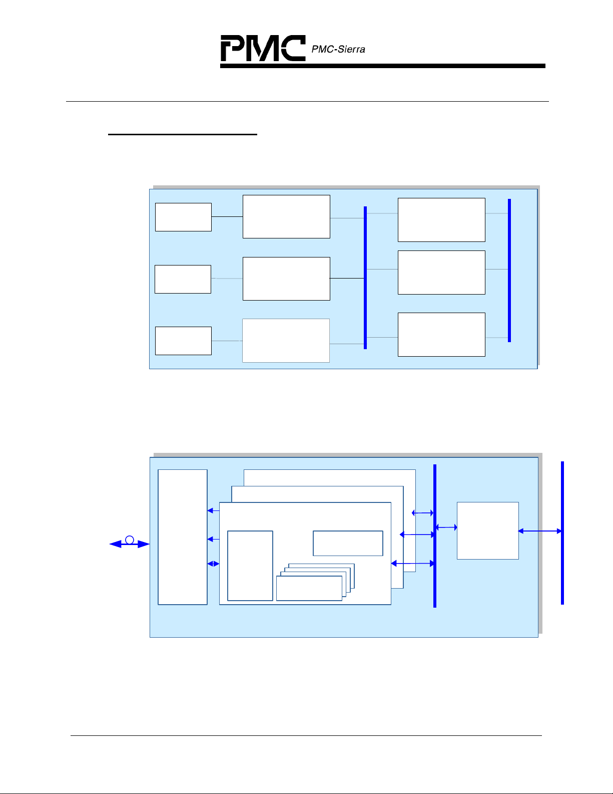
5.1 Top Level Block Diagram
Figure 3 shows the complete TEMAP. Clear Channel T1 links can be multiplexed
into the DS3 or can be mapped into the telecom bus as SONET VT1.5 virtual
tributaries or as SDH TU-11 or TU-12 tributary units, shown at the bottom of the
diagram. Clear Channel E1 links can be mapped into the telecom bus as SONET
VT2 virtual tributaries or as SDH TU-12 tributary units, shown at the bottom of
the diagram. System side access to the T1s and E1s is available as serial clock
and data or the SBI bus. DS3 line side access is via the clock and data interface
for line interface units or DS3 mapped into the SONET/SDH telecom bus.
Unchannelized DS3 system side access is available through a serial clock and
data interface or the SBI bus, both shown at the top of the diagram.
Proprietary and Confidential to PMC-Sierra, Inc. and for its Customers’ Internal Use 17
Page 29
STANDARD PRODUCT
DATASHEET
PMC-1991148 ISSUE 3 HIGH DENSITY VT/TU MAPPER
PM5365 TEMAP
AND M13 MULTIPLEXER
Figure 3 - TEMAP Block Diagram
K
L
/
C
Q
]
8
2
]
:
8
1
K
K
L
L
C
C
T
X
C
[
2
:
K
1
[
L
D
C
E
E
]
E
0
:
R
7
[
_
A
T
A
D
A
S
K
L
T
S
C
P
D
A
S
P
5
L
F
F
U
J
V
P
1
E
A
A
A
C
R
S
S
S
S
S
]
]
0
0
:
:
1
7
[
[
T
A
T
C
T
C
A
A
P
L
5
B
A
D
P
V
D
I
I
B
B
D
D
D
D
S
S
S
S
S
S
]
8
2
]
:
8
1
[
2
:
K
1
L
[
C
D
I
I
O
P
F
1
2
K
K
M
L
L
T
/
C
C
O
V
V
P
C
C
F
E
E
T
R
R
O
S
P
I
R
/
F
P
K
K
F
M
D
L
L
R
M
H
C
/
O
C
I
T
P
R
/
T
P
O
T
I
A
V
A
A
P
A
P
G
D
F
O
D
G
F
R
R
R
T
R
T
T
e
s
c
m
s
F
a
e
I
f
e
t
r
r
S
s
e
g
y
E
t
E
S
n
I
s
n
r
r
o
i
e
t
t
o
t
t
S
i
p
T
a
J
P
O
u
A
l
O
n
J
a
g
t
i
e
T
T
n
t
i
t
g
i
A
m
i
D
T
I
s
I
s
B
e
B
S
r
X
S
g
E
E
l
O
e
l
S
l
I
o
a
P
t
r
I
a
B
P
S
S
B
R
P
s
I
s
I
s
u
B
l
a
i
r
e
S
n
r
e
t
t
a
P
s
B
e
B
u
r
S
S
g
B
N
I
n
I
l
O
l
e
l
P
a
l
I
i
r
o
a
S
t
r
I
e
a
B
S
P
S
r
-
o
r
/
t
r
e
c
o
n
e
t
t
e
a
e
G
D
r
o
I
t
m
a
r
M
r
a
g
L
l
e
A
A
t
n
I
e
c
s
r
n
r
o
N
a
e
t
t
i
O
m
n
n
r
u
M
o
o
f
o
P
r
M
C
e
P
e
s
c
m
s
a
e
F
e
f
I
t
r
r
s
S
g
e
I
y
t
n
S
I
n
I
R
,
t
n
M
n
o
e
i
e
R
t
m
r
c
m
F
m
-
a
a
a
l
n
r
r
1
t
g
A
F
E
i
x
l
/
E
1
A
T
r
r
e
t
o
t
t
i
T
a
J
A
u
l
J
n
a
t
i
e
R
t
g
t
i
A
D
s
r
e
m
a
r
F
g
n
i
r
1
o
E
t
i
1
n
2
o
r
M
o
e
1
c
T
n
8
a
2
m
f
r
o
o
f
e
r
n
e
O
P
X
/
2
1
X
M
R
M
R
F
r
r
o
e
t
e
l
t
p
l
r
a
O
e
p
i
e
l
r
l
S
a
v
I
e
a
n
r
m
P
S
o
a
e
C
P
D
r
y
e
e
r
p
v
a
M
i
t
p
e
D
a
u
c
T
b
e
i
M
R
r
e
R
T
D
P
A
R
T
r
y
o
H
e
r
/
s
P
v
a
i
s
O
t
O
e
e
u
h
c
T
c
b
t
e
i
R
o
a
r
r
R
P
T
P
r
e
e
o
-
F
o
I
r
P
c
i
M
M
]
]
B
B
B
0
0
:
:
S
R
D
3
7
[
C
R
1
W
[
D
A
d
i
c
s
D
3
S
s
a
f
M
S
e
r
p
3
c
D
e
o
t
o
D
r
r
n
I
P
D
B
B
E
M
L
T
T
2
A
S
5
N
I
R
K
L
C
r
o
r
d
s
e
a
U
P
s
p
o
T
P
l
/
e
p
T
y
c
T
a
a
V
o
V
M
r
P
P
]
5
1
L
L
T
T
P
P
0
J
:
D
1
7
[
D
C
A
L
D
T
L
A
D
D
L
K
S
I
P
V
P
D
L
F
S
S
C
A
T
T
L
A
E
D
D
L
S
D
S
E
L
L
W
A
A
D
D
E
E
A
A
D
D
R
R
A
A
R
R
r
l
e
o
t
t
e
l
r
l
O
l
e
a
a
P
i
v
I
r
r
n
a
S
e
o
P
S
C
t
y
i
r
r
e
P
m
a
t
p
s
M
u
p
n
T
b
a
a
i
T
r
r
M
T
T
r
t
i
o
e
t
s
m
m
o
s
r
s
e
a
m
n
l
c
e
a
o
A
r
r
R
T
P
r
t
y
i
o
H
r
/
s
P
a
m
s
t
O
s
O
e
u
h
n
T
t
c
b
a
i
a
T
o
r
r
r
P
T
T
P
r
t
e
i
o
r
d
d
s
e
a
A
i
U
P
m
3
s
p
o
T
S
s
P
M
l
/
S
e
n
T
a
V
r
T
]
K
P
P
0
:
F
C
D
7
T
T
[
A
S
S
L
A
E
E
T
A
W
W
D
D
D
A
A
A
L
R
R
p
3
y
c
T
d
a
D
a
D
o
d
V
M
r
P
A
P
L
1
1
E
K
V
P
L
C
O
1
A
A
C
A
J
L
L
F
L
1
E
C
R
A
L
L
1
#
C
L
R
D
P
H
D
T
x
t
i
T
N
m
3
s
A
S
n
R
D
a
T
r
T
C
C
A
E
O
e
S
F
d
B
Z
o
X
x
c
3
T
n
B
E
K
T
K
L
L
A
C
D
C
I
T
T
T
/
S
O
P
T
n
U
2
X
e
1
M
2
S
D
3
2
X
M
r
e
m
a
r
F
P
F
M
T
/
G
E
N
T
s
M
U
v
2
E
e
M
1
D
S
M
r
/
f
e
o
R
m
e
M
a
r
n
R
F
O
F
X
/
3
U
X
2
M
U
M
E
M
D
r
.
N
o
f
t
i
r
O
n
e
e
r
M
o
P
v
R
e
i
3
P
M
e
M
S
m
c
a
R
D
e
r
F
F
R
C
C
x
L
L
R
D
D
R
H
e
C
S
Z
3
B
C
d
x
O
o
A
R
c
E
B
e
F
R
D
K
T
V
L
A
C
C
L
D
R
R
R
/
/
S
G
E
O
P
N
R
R
s
s
e
c
t
G
r
c
A
o
A
T
P
t
J
s
e
T
I
B
K
S
O
D
T
L
M
D
T
S
C
T
T
T
R
T
Proprietary and Confidential to PMC-Sierra, Inc. and for its Customers’ Internal Use 18
Page 30
STANDARD PRODUCT
DATASHEET
PMC-1991148 ISSUE 3 HIGH DENSITY VT/TU MAPPER
PM5365 TEMAP
AND M13 MULTIPLEXER
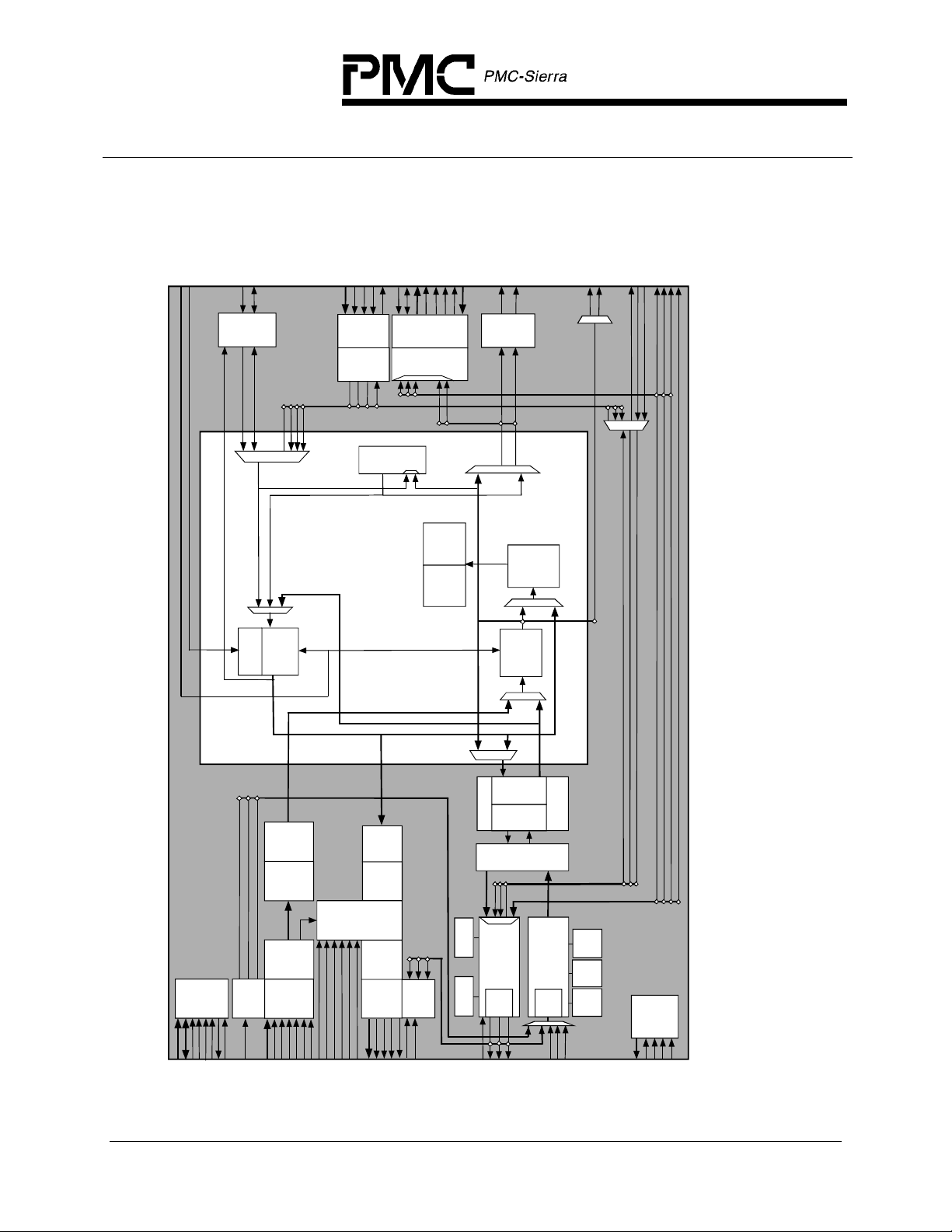
5.2 VT/TU Mapper Only Mode Block Diagram
Figure 4 shows the TEMAP configured as a VT or TU mapper. In this mode the
TEMAP provides access for up to 28 independent unframed 1.544Mb/s streams
or 21 independent unframed 2.048Mb/s streams. The 1.544Mb/s and 2.048Mb/s
streams can be accessed on the system side as clock and data as shown in
Figure 4, or they can be accessed via the SBI bus. The T1 or E1 framers and
performance monitoring blocks can be used to monitor the passing traffic in
either the ingress or egress direction. The M13 Multiplexer mode operates in
much the same way as the VT and TU mapper shown in Figure 4.
Figure 4 - VT/TU Mapper Block Diagram
VT
VT
RTOP
Receive
Tributary
Path O/H
Processor
TRAP/
TTOP
Transmit
Remote
Alarm
&
Tributary
PathO/H
Processors
RTDM
Receive
Tributary
DeMapper
TTMP
Transmit
Tributary
Mapper
PISO
Parallel to
Serial
Converter
SIPO
Serial to
Parallel
Converter
LDDAT A[7:0]
LDC1 J1
LDDP
LDPL
LDT PL
LDV5
LDAIS
LADA TA[7 :0]
LADP
LAPL
LAC1J 1V1
LAOE
LAC1
LREF CLK
RADE AST
RAD EAS LCK
RADE ASTFP
RADW EST
RADW ESTCK
RADW ESTFP
VTPP
Payload
Processor
VTPP
Payload
Processor
XCL K
ECLK [1:2 8]
ED[1 :28]
TJAT
Digital Jitter
Attenuator
PMON
Performance
Monitor
Counters
ALMI
Alarm
Integrator
T1/E1-FRMR
Framer:
Frame
Alignment,
RJAT
Digital Jitter
Attenuator
One of 28 T 1 or
21 E1 Fram ers
Alarm
Extraction
Proprietary and Confidential to PMC-Sierra, Inc. and for its Customers’ Internal Use 19
ID[1:2 8]
ICLK[ 1:28 ]
REC VCL K1
REC VCL K2
Page 31

STANDARD PRODUCT
DATASHEET
PMC-1991148 ISSUE 3 HIGH DENSITY VT/TU MAPPER
PM5365 TEMAP
AND M13 MULTIPLEXER
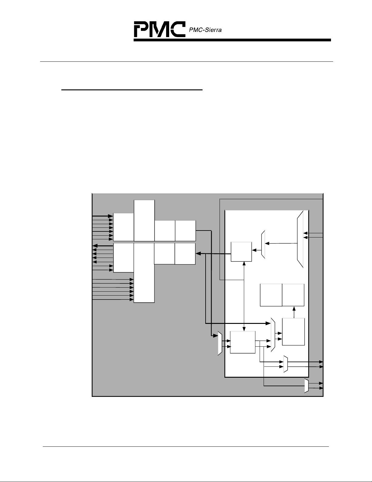
5.3 DS3 Framer Only Block Diagram
Figure 5 shows the TEMAP configured as a DS3 framer. In this mode the
TEMAP provides access to the full DS3 unchannelized payload. The payload
access (right side of diagram) has two clock and data interfacing modes, one
utilizing a gapped clock to mask out the DS3 overhead bits and the second
utilizing an ungapped clock with overhead indications on a separate overhead
signal. The SBI bus can also be used to provide access to the unchannelized
DS3.
Figure 5 - DS3 Framer Only Mode Block Diagram
TDPR
Tx
HDLC
TICLK
TCLK
TPOS/TDAT
TNEG/TMFP
RCLK
RPOS/RDAT
RNEG/RLCV
B3ZS
Encode
B3ZS
Decode
TRAN
DS3
Transmit
Framer
FRMR
DS3
Receive
Framer
TDATI
TFPO/TMFPO/TGAPCLK
TFPI/TMFPI
RGAPCLK/RSCLK
RDATO
RFPO/RMFPO
ROVRHD
RDLC
Rx
HDLC
PMON
Perf.
Monitor
Proprietary and Confidential to PMC-Sierra, Inc. and for its Customers’ Internal Use 20
Page 32

STANDARD PRODUCT
DATASHEET
PMC-1991148 ISSUE 3 HIGH DENSITY VT/TU MAPPER
PM5365 TEMAP
AND M13 MULTIPLEXER
6 DESCRIPTION
The PM5365 VT/TU Mapper and M13 Multiplexer (TEMAP) is a feature-rich
device for use in any applications requiring high density link termination over T1
channelized DS3 or T1 and E1 channelized SONET/SDH facilities.
The TEMAP supports asynchronous multiplexing and demultiplexing of 28 DS1s
into a DS3 signal as specified by ANSI T1.107 and Bell Communications
Research TR-TSY-000009. It supports bit asynchronous mapping and
demapping of 28 T1s or 21 E1s into SONET/SDH as specified by ANSI T1.105,
Bell Communications Research GR-253-CORE and ITU-T Recommendation
G.707. The TEMAP also supports mapping of 21 T1s into SDH via TU-12s. Up to
28 Transparent VT1.5s and TU-11s or 21 Transparent VT2s and TU-12s can be
transferred between the SONET/SDH interface and the SBI bus interface.
Performance monitoring in either the ingress or egress direction for up to 28 T1s
or 21 E1s in both SONET/SDH VT/TU mapper and M13 multiplexer modes.
Each T1 performance monitor detects and indicates the presence of Yellow and
AIS patterns and also integrates Yellow, Red, and AIS alarms. T1 performance
monitoring with accumulation of CRC-6 errors, framing bit errors, out-of-frame
events, and changes of frame alignment is provided.
Each E1 framer detects and indicates the presence of remote alarm and AIS
patterns and also integrates Red and AIS alarms.
The E1 framers support detection of various alarm conditions such as loss of
frame, loss of signaling multiframe and loss of CRC multiframe. The E1 framers
also support reception of remote alarm signal, remote multiframe alarm signal,
alarm indication signal, and time slot 16 alarm indication signal.
E1 performance monitoring with accumulation of CRC-4 errors, far end block
errors and framing bit errors is provided.
This device can also be configured as a DS3 framer, providing external access to
the full DS3 payload, or a VT/TU mapper, providing access to unframed
1.544Mb/s and 2.048Mb/s links.
PRBS generation or detection is supported on a per T1 or E1 link basis.
The TEMAP can generate a low jitter transmit clock from a variety of clock
references, and also provides jitter attenuation in the receive path. Two low jitter
recovered T1 clocks can be routed outside the TEMAP for network timing
applications.
Proprietary and Confidential to PMC-Sierra, Inc. and for its Customers’ Internal Use 21
Page 33

STANDARD PRODUCT
DATASHEET
PMC-1991148 ISSUE 3 HIGH DENSITY VT/TU MAPPER
PM5365 TEMAP
AND M13 MULTIPLEXER
Serial PCM interfaces to each T1 framer allow 1.544 Mbit/s ingress/egress
system interfaces to be directly supported.
A Scaleable Bandwidth Interconnect (SBI) high density byte serial system
interface provides higher levels of integration and dense interconnect. The SBI
bus interconnects up to 84 T1s or 63 E1. The SBI allows transmit timing to be
mastered by either the TEMAP or link layer device connected to the SBI bus.
This interconnect allows up to 3 TEMAPs to be connected in parallel to provide
the full complement of 84 T1s or 63 E1s of traffic. In addition to clear channel
T1s and E1s the TEMAP can transport framed or unframed DS3 links over the
SBI bus.
When configured as a DS3 multiplexer/demultiplexer or DS3 framer, the TEMAP
accepts and outputs either or both digital B3ZS-encoded bipolar and unipolar
signals compatible with M23 and C-bit parity applications.
In the DS3 receive direction, the TEMAP frames to DS3 signals with a maximum
average reframe time of 1.5 ms in the presence of 10
-3
bit error rate and detects
line code violations, loss of signal, framing bit errors, parity errors, C-bit parity
errors, far end block errors, AIS, far end receive failure and idle code. The DS3
framer is an off-line framer, indicating both out of frame (OOF) and change of
frame alignment (COFA) events. The error events (C-BIT, FEBE, etc.) are still
indicated while the framer is OOF, based on the previous frame alignment. When
in C-bit parity mode, the Path Maintenance Data Link and the Far End Alarm and
Control (FEAC) channels are extracted. HDLC receivers are provided for Path
Maintenance Data Link support. In addition, valid bit-oriented codes in the FEAC
channels are detected and are available through the microprocessor port.
Error event accumulation is also provided by the TEMAP. Framing bit errors, line
code violations, excessive zeros occurrences, parity errors, C-bit parity errors,
and far end block errors are accumulated. Error accumulation continues even
while the off-line framers are indicating OOF. The counters are intended to be
-3
polled once per second, and are sized so as not to saturate at a 10
bit error
rate. Transfer of count values to holding registers is initiated through the
microprocessor interface.
In the DS3 transmit direction, the TEMAP inserts DS3 framing, X and P bits.
When enabled for C-bit parity operation, bit-oriented code transmitters and
HDLC transmitters are provided for insertion of the FEAC channels and the Path
Maintenance Data Links into the appropriate overhead bits. Alarm Indication
Signals, Far End Receive Failure and idle signal can be inserted using either
internal registers or can be configured for automatic insertion upon received
errors. When M23 operation is selected, the C-bit Parity ID bit (the first C-bit of
the first M sub-frame) is forced to toggle so that downstream equipment will not
confuse an M23-formatted stream with stuck-at-1 C-bits for C-bit Parity
Proprietary and Confidential to PMC-Sierra, Inc. and for its Customers’ Internal Use 22
Page 34

STANDARD PRODUCT
DATASHEET
PMC-1991148 ISSUE 3 HIGH DENSITY VT/TU MAPPER
PM5365 TEMAP
AND M13 MULTIPLEXER
application. Transmit timing is from an external reference or from the receive
direction clock.
The TEMAP also supports diagnostic options which allow it to insert a Pseudo
Random Binary Sequence (PRBS) into a DS3 payload and checked in the
receive DS3 payload for bit errors. A fixed 100100… pattern is available for
insertion directly into the B3ZS encoder for proper pulse mask shape verification.
When configured in DS3 multiplexer mode, seven 6312 kbit/s data streams are
demultiplexed and multiplexed into and out of the DS3 signal. Bit stuffing and
rate adaptation is performed. The C-bits are set appropriately, with the option of
inserting DS2 loopback requests. Interrupts can be generated upon detection of
loopback requests in the received DS3. AIS may be inserted in the any of the
6312 kbit/s tributaries in both the multiplex and demultiplex directions. C-bit
parity is supported by generating a 6.3062723 MHz clock, which corresponds to
a stuffing ratio of 100%.
Framing to the demultiplexed 6312 kbit/s data streams supports DS2 (ANSI
TI.107) frame formats. The maximum average reframe time is 7ms for DS2. Far
end receive failure is detected and M-bit and F-bit errors are accumulated. The
DS2 framer is an off-line framer, indicating both OOF and COFA events. Error
events (FERF, MERR, FERR, PERR, RAI, framing word errors) are still indicated
while the DS2 framer is indicating OOF, based on the previous alignment.
Each of the seven 6312 kbit/s multiplexers may be independently configured to
multiplex and demultiplex four 1544 kbit/s DS1s into and out of a DS2 formatted
signal. Tributary frequency deviations are accommodated using internal FIFOs
and bit stuffing. The C-bits are set appropriately, with the option of inserting DS1
loopback requests. Interrupts can be generated upon detection of loopback
requests in the received DS2. AIS may be inserted in any of the low speed
tributaries in both multiplex and demultiplex directions.
When configured as a DS3 framer the unchannelized payload of the DS3 link is
available to an external device.
The SONET/SDH line side interface provides STS-1 SPE synchronous payload
envelope processing and generation, TUG3 tributary unit group processing and
generation within a VC4 virtual container and VC3 virtual container processing
and generation. The payload processor aligns and monitors the performance of
SONET virtual tributaries (VTs) or SDH tributary units (TUs). Maintenance
functions per tributary include detection of loss of pointer, AIS alarm, tributary
path signal label mismatch and tributary path signal label unstable alarms.
Optionally interrupts can be generated due to the assertion and removal of any
of the above alarms. Counts are accumulated for tributary path BIP-2 errors on a
block or bit basis and for FEBE indications. The synchronous payload envelope
generator generates all tributary pointers and calculates and inserts tributary
Proprietary and Confidential to PMC-Sierra, Inc. and for its Customers’ Internal Use 23
Page 35

STANDARD PRODUCT
DATASHEET
PMC-1991148 ISSUE 3 HIGH DENSITY VT/TU MAPPER
PM5365 TEMAP
AND M13 MULTIPLEXER
path BIP-2. The generator also inserts FEBE, RDI and enhanced RDI in the V5
byte. Software can force AIS insertion on a per tributary basis.
A SONET/SDH mapper maps and demaps up to 28 T1s, 21 E1s or a single DS3
into a STS-1 SPE, TUG3 or VC3 through an elastic store. The fixed stuff (R) bits
are all set to zeros or ones under microprocessor control. The bit asynchronous
demapper performs majority vote C-bit decoding to detect stuff requests for T1,
E1 and DS3 asynchronous mappings. The VT1.5/VT2/TU-11/TU-12 mapper
uses an elastic store and a jitter attenuator capability to minimize jitter
introduced via bit stuffing.
The TEMAP is configured, controlled and monitored via a generic 8-bit
microprocessor bus through which all internal registers are accessed. All
sources of interrupts can be masked and acknowledged through the
microprocessor interface.
Proprietary and Confidential to PMC-Sierra, Inc. and for its Customers’ Internal Use 24
Page 36

A
Y
AA A
STANDARD PRODUCT
DATASHEET
PMC-1991148 ISSUE 3 HIGH DENSITY VT/TU MAPPER
PM5365 TEMAP
AND M13 MULTIPLEXER
7 PIN DIAGRAM
The TEMAP is currently planned to be packaged in a 324-pin PBGA package
having a body size of 23mm by 23mm and a ball pitch of 1.0 mm. The center 36
balls are not used as signal I/Os and are thermal balls. Pin names and locations
are defined in the Pin Description Table in section 8. Mechanical information for
this package is in the section 19.
Figure 6 - Pin Diagram
22 21 20 19 18 17 16 15 14 13 12 11 10 9 8 7 6 5 4 3 2 1
B
C
D
E
F
G
H
J
K
L
M
N
P
R
T
U
V
W
324 PBGA
VSS VSS VSS VSS VSS VSS
VSS VSS VSS VSS VSS VSS
VSS VSS VSS VSS VSS VSS
VSS VSS VSS VSS VSS VSS
VSS VSS VSS VSS VSS VSS
VSS VSS VSS VSS VSS VSS
Bottom View
B
22 21 20 19 18 17 16 15 14 13 12 11 10 9 8 7 6 5 4 3 2 1
Proprietary and Confidential to PMC-Sierra, Inc. and for its Customers’ Internal Use 25
Page 37

A
STANDARD PRODUCT
DATASHEET
PMC-1991148 ISSUE 3 HIGH DENSITY VT/TU MAPPER
PM5365 TEMAP
AND M13 MULTIPLEXER
8 PIN DESCRIPTION
Pin Name Type Pin
Function
No.
DS3 Line Side Interface
RCLK Input W5
Receive Input Clock (RCLK). RCLK provides the
receive direction timing. RCLK is a DS3, nominally a
44.736 MHz, 50% duty cycle clock input.
RPOS/RDAT
Input Y7
Positive Input Pulse (RPOS). RPOS represents the
positive pulses received on the B3ZS-encoded DS3
when dual rail input format is selected.
Receive Data Input (RDAT). RDAT represents the
NRZ (unipolar) DS3 input data stream when single rail
input format is selected.
RPOS and RDAT are sampled on the rising edge of
RCLK by default and may be enabled to be sampled
on the falling edge of RCLK by setting the RFALL bit in
the DS3 Master Receive Line Options register.
RNEG/RLCV
Input AB6
Negative Input Pulse (RNEG). RNEG represents the
negative pulses received on the B3ZS-encoded DS3
when dual rail input format is selected.
Line code violation (RLCV). RLCV represents receive
line code violations when single rail input format is
selected.
RNEG and RLCV are sampled on the rising edge of
RCLK by default and may be enabled to be sampled
on the falling edge of RCLK by setting the RFALL bit in
the DS3 Master Receive Line Options register.
TCLK Output
A7
Transmit Clock (TCLK). TCLK provides timing for
circuitry downstream of the DS3 transmitter of the
TEMAP. TCLK is nominally a 44.736 MHz, 50% duty
cycle clock.
Proprietary and Confidential to PMC-Sierra, Inc. and for its Customers’ Internal Use 26
Page 38

A
A
STANDARD PRODUCT
DATASHEET
PMC-1991148 ISSUE 3 HIGH DENSITY VT/TU MAPPER
PM5365 TEMAP
AND M13 MULTIPLEXER
Pin Name Type Pin
Function
No.
TPOS/TDAT Output
B7
Transmit Positive Pulse (TPOS). TPOS represents
the positive pulses transmitted on the B3ZS-encoded
DS3 line when dual-rail output format is selected.
Transmit Data Output (TDAT). TDAT represents the
NRZ (unipolar) DS3 output data stream when single
rail output format is selected.
TPOS and TDAT are updated on the falling edge of
TCLK by default but may be enabled to be updated on
the rising edge of TCLK by setting the TRISE bit in the
DS3 Master Transmit Line Options register. TPOS and
TDAT are updated on TICLK rather than TCLK when
the TICLK bit in the DS3 Master Transmit Line Options
register is set.
TNEG/TMFP Output W6
Transmit Negative Pulse (TNEG). TNEG represents
the negative pulses transmitted on the B3ZS-encoded
DS3 line when dual-rail output format is selected.
Transmit Multiframe Pulse (TMFP). This signal
marks the transmit M-frame alignment when
configured for single rail operation. TMFP indicates
the position of overhead bits in the transmit
transmission system stream, TDAT. TMFP is high
during the first bit (X1) of the multiframe.
TNEG and TMFP are updated on the falling edge of
TCLK by default but may be enabled to be updated on
the rising edge of TCLK by setting the TRISE bit in the
DS3 Master Transmit Line Options register. TNEG and
TMFP are updated on TICLK rather than TCLK when
the TICLK bit in the DS3 Master Transmit Line Options
register is set.
TICLK Input
A6
Transmit input clock (TICLK). TICLK provides the
transmit direction timing. TICLK is nominally a 44.736
MHz, 50% duty cycle clock.
This clock is only required when using the DS3
transmitter, either with the DS3 line side interface or
the DS3 mapper. When not used this clock input
should be connected to ground.
Proprietary and Confidential to PMC-Sierra, Inc. and for its Customers’ Internal Use 27
Page 39

STANDARD PRODUCT
DATASHEET
PMC-1991148 ISSUE 3 HIGH DENSITY VT/TU MAPPER
PM5365 TEMAP
AND M13 MULTIPLEXER
Pin Name Type Pin
Function
No.
XCLK/VCLK Input E20
Crystal Clock Input (XCLK). This 24 times T1 or E1
clock provides timing for many of the T1 and E1
portions of TEMAP. XCLK is nominally a 37.056 MHz
± 32ppm, 50% duty cycle clock when configured for T1
modes and is nominally a 49.152 MHz ± 32ppm, 50%
duty cycle clock when configured for E1 modes.
This clock is required for all operating modes of the
TEMAP.
Test Vector Clock (VCLK). This signal is used during
production testing.
Proprietary and Confidential to PMC-Sierra, Inc. and for its Customers’ Internal Use 28
Page 40

A
STANDARD PRODUCT
DATASHEET
PMC-1991148 ISSUE 3 HIGH DENSITY VT/TU MAPPER
PM5365 TEMAP
AND M13 MULTIPLEXER
Pin Name Type Pin
No.
DS3 System Side Interface
RGAPCLK/RSCLK Output Y3
Function
Framer Recovered Gapped Clock (RGAPCLK).
RGAPCLK is valid when the TEMAP is configured as a
DS3 framer by setting the OPMODE[1:0] bits in the
Global Configuration register and the RXGAPEN bit in
the DS3 Master Unchannelized Interface Options
register.
RGAPCLK is the recovered clock and timing reference
for RDATO. RGAPCLK is held either high or low
during bit positions which correspond to overhead.
Framer Recovered Clock (RSCLK). RSCLK is valid
when the TEMAP is configured as a DS3 framer by
setting the OPMODE[1:0] bits in the Global
Configuration register.
RSCLK is the recovered clock and timing reference for
RDATO, RFPO/RMFPO, and ROVRHD.
This signal shares a signal pin with ICLK[1]. When
enabled for unchannelized DS3 operation this signal
will be RGAPCLK/RSCLK, otherwise it will be ICLK[1].
RDATO Output
A5
Framer Receive Data (RDATO). RDATO is valid when
the TEMAP is configured as a DS3 framer by setting
the OPMODE[1:0] bits in the Global Configuration
register. RDATO is the received data aligned to
RFPO/RMFPO and ROVRHD.
RDATO is updated on either the falling or rising edge
of RGAPCLK or RSCLK, depending on the value of
the RSCLKR bit in the DS3 Master Unchannelized
Interface Options register. By default RDATO will be
updated on the falling edge of RGAPCLK or RSCLK.
This signal shares a signal pin with ID[1] and MVID[1].
This signal will be RDATO only when enabled for
unchannelized DS3 operation.
Proprietary and Confidential to PMC-Sierra, Inc. and for its Customers’ Internal Use 29
Page 41

STANDARD PRODUCT
DATASHEET
PMC-1991148 ISSUE 3 HIGH DENSITY VT/TU MAPPER
PM5365 TEMAP
AND M13 MULTIPLEXER
Pin Name Type Pin
No.
RFPO/RMFPO Output AB5
Function
Framer Receive Frame Pulse/Multi-frame Pulse
(RFPO/RMFPO). RFPO/RMFPO is valid when the
TEMAP is configured to be in framer only mode by
setting the OPMODE[1:0] bits in the Global
Configuration register.
RFPO is aligned to RDATO and indicates the position
of the first bit in each DS3 M-subframe.
RMFPO is aligned to RDATO and indicates the
position of the first bit in each DS3 M-frame. This is
selected by setting the RXMFPO bit in the Master
Framer Configuration Registers.
RFPO/RMFPO is updated on either the falling or rising
edge of RSCLK depending on the setting of the
RSCLKR bit in the DS3 Master Unchannelized
Interface Options register.
This signal shares a signal pin with IFP[1]. When
enabled for unchannelized DS3 operation this signal
will be RFPO/RMFPO, otherwise it will be IFP[1].
ROVRHD Output Y6
Framer Receive Overhead (ROVRHD). ROVRHD is
valid when the TEMAP is configured as a DS3 framer
by setting the OPMODE[1:0] bits in the Global
Configuration register.
ROVRHD will be high whenever the data on RDATO
corresponds to an overhead bit position. ROVRHD is
updated on the either the falling or rising edge of
RSCLK depending on the setting of the RSCLKR bit in
the DS3 Master Unchannelized Interface Options
register.
This signal shares a signal pin with ID[2]. This signal
will be ROVRHD only when enabled for unchannelized
DS3 operation.
Proprietary and Confidential to PMC-Sierra, Inc. and for its Customers’ Internal Use 30
Page 42

STANDARD PRODUCT
DATASHEET
PMC-1991148 ISSUE 3 HIGH DENSITY VT/TU MAPPER
PM5365 TEMAP
AND M13 MULTIPLEXER
Pin Name Type Pin
No.
TFPO/TMFPO/
Output AB3
TGAPCLK
Function
Framer Transmit Frame Pulse/Multi-frame Pulse
Reference (TFPO/TMFPO). TFPO/TMFPO is valid
when the TEMAP is configured as a DS3 framer by
setting the OPMODE[1:0] bits in the Global
Configuration register and setting the TXGAPEN bit to
0 in the DS3 Master Unchannelized Interface Options
register.
TFPO pulses high for 1 out of every 85 clock cycles,
giving a reference M-subframe indication.
TMFPO pulses high for 1 out of every 4760 clock
cycles, giving a reference M-frame indication.
TFPO/TMFPO is updated on the falling edge of TICLK.
TFPO/TMFPO can be configured to be updated on the
rising edge of TICLK by setting the TDATIFALL bit to
1in the DS3 Master Unchannelized Interface Options
register..
Framer Gapped Transmit Clock (TGAPCLK).
TGAPCLK is valid when the TEMAP is configured as a
DS3 framer by setting the OPMODE[1:0] bits in the
Global Configuration register and setting the
TXGAPEN bit to 1 in the DS3 Master Unchannelized
Interface Options register.
TGAPCLK is derived from the transmit reference clock
TICLK or from the receive clock if loop-timed. The
overhead bit (gapped) positions are generated internal
to the device. TGAPCLK is held high during the
overhead bit positions. This clock is useful for
interfacing to devices which source payload data only.
TGAPCLK is used to sample TDATI and TFPI/TMFPI
when TXGAPEN is set to 1.
This signal shares a signal pin with ECLK[1]. When
enabled for unchannelized DS3 operation this signal
will be TFPO/TMFPO/TGAPCLK, otherwise it will be
ECLK[1].
Proprietary and Confidential to PMC-Sierra, Inc. and for its Customers’ Internal Use 31
Page 43

A
STANDARD PRODUCT
DATASHEET
PMC-1991148 ISSUE 3 HIGH DENSITY VT/TU MAPPER
PM5365 TEMAP
AND M13 MULTIPLEXER
Pin Name Type Pin
Function
No.
TDATI Input
B4
Framer Transmit Data (TDATI). TDATI contains the
serial data to be transmitted when the TEMAP is
configured as a DS3 framer by setting the
OPMODE[1:0] bits in the Global Configuration register.
TDATI is sampled on the rising edge of TICLK if the
TXGAPEN bit in the DS3 Master Unchannelized
Interface Options register is logic 0. If TXGAPEN is
logic 1, then TDATI is sampled on the rising edge of
TGAPCLK. TDATI can be configured to be sampled on
the falling edge of TICLK or TGAPCLK by setting the
TDATIFALL bit in the DS3 Master Unchannelized
Interface Options register.
This signal shares a signal pin with ED[1] and
MVED[1]. This signal will be TDATI only when enabled
for unchannelized DS3 operation.
TFPI/TMFPI Input AA3
Framer Transmit Frame Pulse/Multiframe Pulse
(TFPI/TMFPI). TFPI/TMFPI is valid when the TEMAP
is configured as a DS3 framer by setting the
OPMODE[1:0] bits in the Global Configuration register.
TFPI indicates the position of all overhead bits in each
DS3 M-subframe. TFPI is not required to pulse at
every frame boundary.
TMFPI indicates the position of the first bit in each DS3
M-frame. TMFPI is not required to pulse at every
multiframe boundary.
TFPI/TMFPI is sampled on the rising edge of TICLK if
the TXGAPEN bit in the DS3 Master Unchannelized
Interface Options register is logic 0. If TXGAPEN is
logic 1, then TFPI/TMFPI is sampled on the rising edge
of TGAPCLK. TFPI/TMFPI can be configured to be
sampled on the falling edge of TICLK or TGAPCLK by
setting the TDATIFALL bit to 1in the DS3 Master
Unchannelized Interface Options register.
This signal shares a signal pin with ED[2]. This signal
will be TFPI/TMFPI only when enabled for
unchannelized DS3 operation.
Proprietary and Confidential to PMC-Sierra, Inc. and for its Customers’ Internal Use 32
Page 44

A
A
A
A
STANDARD PRODUCT
DATASHEET
PMC-1991148 ISSUE 3 HIGH DENSITY VT/TU MAPPER
PM5365 TEMAP
AND M13 MULTIPLEXER
Pin Name Type Pin
Function
No.
T1 and E1 System Side Serial Clock and Data Interface
ICLK[1]
ICLK[2]
ICLK[3]
ICLK[4]
ICLK[5]
ICLK[6]
ICLK[7]
ICLK[8]
ICLK[9]
ICLK[10]
ICLK[11]
ICLK[12]
ICLK[13]
ICLK[14]
ICLK[15]
ICLK[16]
ICLK[17]
ICLK[18]
ICLK[19]
ICLK[20]
ICLK[21]
ICLK[22]
ICLK[23]
ICLK[24]
ICLK[25]
ICLK[26]
ICLK[27]
ICLK[28]
Output Y3
B2
B20
B21
W22
Y20
H22
F19
W3
A1
H3
H1
L22
K19
F22
G20
T3
U1
D1
C1
H19
G19
E19
F21
K3
J4
E3
D2
Ingress Clocks (ICLK[1:28]). The Ingress Clocks are
active when the external signaling interface is disabled.
Each ingress clock is optionally a smoothed (jitter
attenuated) version of the associated receive clock
from either the SONET/SDH mapper or the DS3
multiplexer. When the Clock Master: NxChannel mode
is active, ICLK[x] is a gapped version of the smoothed
receive clock. When Clock Master: Full T1/E1 mode is
active, IFP[x] and ID[x] are updated on the active edge
of ICLK[x]. When the Clock Master: NxDS0 mode is
active, ID[x] is updated on the active edge of ICLK[x].
In E1 mode only ICLK[1:21] is used.
ICLK[1] shares a pin with the DS3 system interface
signal RGAPCLK/RSCLK.
Proprietary and Confidential to PMC-Sierra, Inc. and for its Customers’ Internal Use 33
Page 45

A
A
A
A
STANDARD PRODUCT
DATASHEET
PMC-1991148 ISSUE 3 HIGH DENSITY VT/TU MAPPER
PM5365 TEMAP
AND M13 MULTIPLEXER
Pin Name Type Pin
No.
ID[1]
ID[2]
ID[3]
ID[4]
ID[5]
ID[6]
ID[7]
ID[8]
ID[9]
ID[10]
ID[11]
ID[12]
ID[13]
ID[14]
ID[15]
ID[16]
ID[17]
ID[18]
ID[19]
ID[20]
ID[21]
ID[22]
ID[23]
ID[24]
ID[25]
ID[26]
ID[27]
ID[28]
Output AA5
Y6
A20
T19
R19
P20
G22
G21
Y2
W2
G4
H2
P21
P22
12
D12
U2
V4
D11
11
M19
L19
D10
10
J1
H4
B10
C10
Function
Ingress Data (ID[1:28]). Each ID[x] signal contains
the recovered data stream.
ID[x] is aligned to the receive line timing and is
updated on the active edge of the associated ICLK[x].
In E1 mode only ID[1:21] are used.
ID[1] shares a pin with the DS3 system interface signal
RDATO. ID[2] shares a pin with the DS3 system
interface signal ROVRHD. ID[15,16,19,20,23,24,27,28]
shares pins with the SBI interface bus SDDATA[7:0].
Proprietary and Confidential to PMC-Sierra, Inc. and for its Customers’ Internal Use 34
Page 46

j
STANDARD PRODUCT
DATASHEET
PMC-1991148 ISSUE 3 HIGH DENSITY VT/TU MAPPER
PM5365 TEMAP
AND M13 MULTIPLEXER
Pin Name Type Pin
Function
No.
CTCLK Input M3
Common Transmit Clock (CTCLK). This input signal
is used as a reference transmit tributary clock which
can be used in egress Clock Master: Clear Channel
mode. Depending on the configuration of the TEMAP,
CTCLK may be a line rate clock (so the transmit clock
is generated directly from CTCLK, or from CTCLK after
itter attenuation) or a multiple of 8kHz (Nx8khz, where
1£N£256) so long as CTCLK is jitter-free when divided
down to 8kHz (in which case the transmit clock is
derived by the DJAT PLL using CTCLK as a
reference).
The TEMAP may be configured to ignore the CTCLK
input and utilize one of the recovered Ingress clocks
instead, RECVCLK1 and RECVCLK2. Receive
tributary clock[x] is automatically substituted for CTCLK
if line loopback is enabled.
Proprietary and Confidential to PMC-Sierra, Inc. and for its Customers’ Internal Use 35
Page 47

A
A7 A
A
A
A
STANDARD PRODUCT
DATASHEET
PMC-1991148 ISSUE 3 HIGH DENSITY VT/TU MAPPER
PM5365 TEMAP
AND M13 MULTIPLEXER
Pin Name Type Pin
No.
ED[1]
ED[2]
ED[3]
ED[4]
ED[5]
ED[6]
Input AB4
A3
P19
N20
N21
N22
ED[7]
ED[8]
ED[9]
ED[10]
ED[11]
ED[12]
ED[13]
ED[14]
ED[15]
ED[16]
ED[17]
ED[18]
ED[19]
ED[20]
ED[21]
ED[22]
ED[23]
ED[24]
ED[25]
ED[26]
ED[27]
ED[28]
2
T2
R4
3
B4
N19
M22
D6
C7
P2
M1
D4
B6
C20
E22
5
B5
L1
L2
4
C5
Function
Egress Data (ED[1:28]). The egress data streams to
be transmitted are input on these pins. When the
Clock Master Clear Channel mode is active, ED[x] is
sampled on the active edge of ECLK[x]. When the
Clock Slave: Clear channel mode is active, ED[x] is
sampled on the active edge of ECLK[x].
In E1 mode only ED[1:21] are used.
ED[1] shares a pin with the DS3 system interface
signal TDATI. ED[2] shares a pin with the DS3 system
interface signal TFPI/TMFPI.
ED[7,8,11,12,15,16,19,20,23,24,27,28] shares pins
with the SBI interface add bus signals.
Proprietary and Confidential to PMC-Sierra, Inc. and for its Customers’ Internal Use 36
Page 48

A
A
A
A
STANDARD PRODUCT
DATASHEET
PMC-1991148 ISSUE 3 HIGH DENSITY VT/TU MAPPER
PM5365 TEMAP
AND M13 MULTIPLEXER
Pin Name Type Pin
No.
ECLK[1]
ECLK[2]
ECLK[3]
ECLK[4]
ECLK[5]
ECLK[6]
ECLK[7]
ECLK[8]
ECLK[9]
ECLK[10]
ECLK[11]
ECLK[12]
ECLK[13]
ECLK[14]
ECLK[15]
ECLK[16]
ECLK[17]
ECLK[18]
ECLK[19]
ECLK[20]
ECLK[21]
ECLK[22]
ECLK[23]
ECLK[24]
ECLK[25]
ECLK[26]
ECLK[27]
ECLK[28]
I/O
B3
Y4
Y19
A21
B22
V22
T21
T22
B1
T1
G2
G3
U21
V19
D21
C21
U4
R1
D3
F1
T20
U22
B22
D20
L3
K4
E4
F2
Function
Egress Clock (ECLK[1:28]). When the Clock Master
Clear Channel mode is active, ECLK[x] is an output
and is used to sample the associated egress data,
ED[x]. ECLK[x] is a version of the transmit clock[x]
which is generated from the receive clock or the
common transmit clock, CTCLK.
When in Clock Slave: Clear Channel mode ECLK[x] is
an input and is used to sampled ED[x].
ED[x] is sampled on the active edge of the associated
ECLK[x].
ECLK[1] shares a pin with the DS3 system interface
output signal TFPO/TMFPO/TGAPCLK.
Recovered T1 and E1 Clocks
RECVCLK1 Output D22
Recovered Clock 1 (RECVCLK1). This clock output is
a recovered and de-jittered clock from any one of the
28 T1 framers or 21 E1 framers.
RECVCLK2 Output C22
Recovered Clock 2 (RECVCLK2). This clock output is
a recovered and de-jittered clock from any one of the
28 T1 framers or 21 E1 framers.
Telecom Line Side Interface
Proprietary and Confidential to PMC-Sierra, Inc. and for its Customers’ Internal Use 37
Page 49

STANDARD PRODUCT
DATASHEET
PMC-1991148 ISSUE 3 HIGH DENSITY VT/TU MAPPER
PM5365 TEMAP
AND M13 MULTIPLEXER
Pin Name Type Pin
No.
LREFCLK Input W12
LAC1 Input W13
Function
Line Reference Clock (LREFCLK). This signal
provides reference timing for the SONET telecom bus
interface. On the incoming byte interface of the
telecom bus, LDC1J1V1, LDDATA[7:0], LDDP, LDPL,
LDTPL, LDV5, LDAIS and LAC1 are sampled of the
rising edge or LREFCLK. In the outgoing byte
interface, LADATA[7:0], LADP, LAPL, LAC1J1V1 and
LAOE are updated on the rising edge of LREFCLK.
This clock is nominally a 19.44MHz +/-20ppm clock
with a 50% duty cycle. This clock can be external
connected to SREFCLK. When in Transparent VT
mode this clock must be connected to SREFCLK.
Line Add C1 Frame Pulse (LAC1). The Add bus
timing signal identifies the frame and multiframe
boundaries on the Add Data bus LADATA[7:0].
LAC1 is set high to mark the first C1 byte of the first
transport envelope frame of the 4 frame multiframe on
the LADATA[7:0] bus. LAC1 need not be presented on
every occurrence of the multiframe .
LAC1 is sampled on the rising edge of LREFCLK.
Proprietary and Confidential to PMC-Sierra, Inc. and for its Customers’ Internal Use 38
Page 50

A
A
A
STANDARD PRODUCT
DATASHEET
PMC-1991148 ISSUE 3 HIGH DENSITY VT/TU MAPPER
PM5365 TEMAP
AND M13 MULTIPLEXER
Pin Name Type Pin
Function
No.
LAC1J1V1 Output
A11
Line Add Bus Composite Timing Signal
(LAC1J1V1). The Add bus composite timing signal
identifies the frame, payload and tributary multiframe
boundaries on the Line Add Data bus LADATA[7:0].
LAC1J1V1 pulses high with the Line Add Payload
(STM-0/AU3) identification byte or equivalently the
STM identification byte C1. Optionally the LAC1J1V1
signal pulses high with LAPL set high to mark the path
trace byte J1. Optionally the LAC1J1V1 signal pulses
high on the V1 byte to indicate tributary multiframe
boundaries.
In a system with multiple TEMAPs sharing the same
Line Add bus only one device should have LAC1J1V1
connected. All devices must be configured via the
LOCK0 bits in the Master SONET/SDH Configuration
and TTMP Telecom Interface Configuartion registers
for the same J1 location corresponding to a pointer
offset of 0 or 522.
ctive signal LAPL set low to mark the first STS-1
LAC1J1V1 is updated on the rising edge of LREFCLK.
LAOE Output
B11
Line Add Bus Output Enable (LAOE). The Add Bus
output enable signal is asserted high whenever the
Line Add Bus is being driven which is co-coincident
with the Line Add bus outputs coming out of tri-state.
This pin is intended to control an external multiplexer
when multiple TEMAPs are driving the telecom Add
bus during their individual tributaries. This same
function is accomplished with the Add bus tristate
drivers but increased tolerance to tributary
configuration problems is possible with an external
mux. This output is controlled via the LAOE bit in the
TTMP Tributary Control registers.
LAOE is updated on the rising edge of LREFCLK.
Proprietary and Confidential to PMC-Sierra, Inc. and for its Customers’ Internal Use 39
Page 51

A
A
A
A
STANDARD PRODUCT
DATASHEET
PMC-1991148 ISSUE 3 HIGH DENSITY VT/TU MAPPER
PM5365 TEMAP
AND M13 MULTIPLEXER
Pin Name Type Pin
Function
No.
LADATA[0]
LADATA[1]
LADATA[2]
LADATA[3]
LADATA[4]
LADATA[5]
LADATA[6]
LADATA[7]
Output
Tristate
B8
W7
W8
B9
W9
Y10
A10
B10
Line Add Bus Data (LADATA[7:0]). The add bus data
contains the SONET transmit payload data in byte
serial format. All transport overhead bytes are set to
00h. The phase relation of the SPE (VC) to the
transport frame is determined by the Add Bus
composite timing signal LAC1J1V1 and is SW
selectable to be either 0 or 522. LADATA[7] is the most
significant bit (corresponding to bit 1 of each serial
word, the first bit to be transmitted).
LADATA[7:0] is only asserted during the SONET/SDH
tributaries assigned to this device as determined by the
LAOE bit in the TTMP Tributary Control registers.
LADATA[7:0] is updated on the rising edge of
LREFCLK.
LADP Output
Tristate
W10
Line Add Bus Data Parity (LADP). The Add Bus data
parity signal carries the parity of the outgoing signals.
The parity calculation encompasses the LADATA[7:0]
bus and optionally the LAC1J1V1 and LAPL signals.
LAC1J1V1 and LAPL can be included in the parity
calculation by setting the INCLAC1J1V1 and INCLAPL
register bits in the Master SONET/SDH Egress
Configuration register high, respectively. Odd parity is
selected by setting the LAOP register bit in the same
register high and even parity is selected by setting the
LAOP bit low.
LADP is only asserted during the SONET/SDH
tributaries assigned to this device as determined by the
LAOE bit in the TTMP Tributary Control registers.
LADP is updated on the rising edge of LREFCLK.
LAPL Output
Tristate
Y11
Line Add Bus Payload Active (LAPL). The Add Bus
payload active signal identifies the payload bytes on
LADATA[7:0]. LAPL is set high during path overhead
and payload bytes and low during transport overhead
bytes.
LAPL is only asserted during the SONET/SDH
tributaries assigned to this device as determined by the
LAOE bit in the TTMP Tributary Control registers.
LAPL is updated on the rising edge of LREFCLK.
Proprietary and Confidential to PMC-Sierra, Inc. and for its Customers’ Internal Use 40
Page 52

A
A
A
STANDARD PRODUCT
DATASHEET
PMC-1991148 ISSUE 3 HIGH DENSITY VT/TU MAPPER
PM5365 TEMAP
AND M13 MULTIPLEXER
Pin Name Type Pin
Function
No.
LDDATA[0]
LDDATA[1]
LDDATA[2]
LDDATA[3]
LDDATA[4]
LDDATA[5]
LDDATA[6]
LDDATA[7]
LDDP Input
Input AA13
Y13
W14
B14
W15
W16
B15
W17
B16
Line Drop Bus Data (LDDATA[7:0]). The drop bus
data contains the SONET/SDH receive payload data in
byte serial format. LDDATA[7] is the most significant
bit, corresponding to bit 1 of each serial word, the bit
transmitted first.
LDDATA[7:0] is sampled on the rising edge of
LREFCLK.
Line Drop Bus Data Parity (LDDP). The incoming
data parity signal carries the parity of the incoming
signals. The parity calculation encompasses the
LDDATA[7:0] bus and optionally the LDPL signal.
LDPL can be included in the parity calculation by
setting the INCLDPL bit in the Master SONET/SDH
Ingress Configuration register high. Odd parity is
selected by setting the LDOP bit in the Master
SONET/SDH Ingress Configuration register high and
even parity is selected by setting the LDOP bit low.
LDDP is sampled on the rising edge of LREFCLK.
LDC1J1V1 Input Y16
Line Drop C1/J1 Frame Pulse (LDC1J1V1). The
input C1/J1/V1 frame pulse identifies the transport
envelope, synchronous payload envelope frame
boundaries and optionallly multiframe alignment on the
incoming SONET stream.
LDC1J1V1 is set high while LDPL is low to mark the
first C1 byte of the transport envelope frame on the
LDDATA[7:0] bus. LDC1J1V1 is set high while LDPL is
high to mark each J1 byte of the synchronous payload
envelope(s) on the LDDATA[7:0] bus. LDC1J1V1 must
be present at every occurrence of the first C1 and all
J1 bytes.
Optionally LDC1J1V1 indicates multiframe alignment
when high during the first V1 bytes of each envelope.
LDC1J1V1 is sampled on the rising edge of LREFCLK.
Proprietary and Confidential to PMC-Sierra, Inc. and for its Customers’ Internal Use 41
Page 53

A
A
A
A
STANDARD PRODUCT
DATASHEET
PMC-1991148 ISSUE 3 HIGH DENSITY VT/TU MAPPER
PM5365 TEMAP
AND M13 MULTIPLEXER
Pin Name Type Pin
Function
No.
LDPL Input
A16
Line Drop Bus Payload Active (LDPL). The payload
active signal identifies the bytes on LDDATA[7:0] that
carry payload bytes.
LDPL is set high during path overhead and payload
bytes and low during transport overhead bytes. LDPL
is set high during the H3 byte to indicate a negative
pointer justification and low during the byte following
H3 to indicate a positive pointer justification event.
LDPL is sampled on the rising edge of LREFCLK.
LDV5 Input
B17
Line Drop Bus V5 Byte (LDV5). The incoming
tributary V5 byte signal marks the various tributary V5
bytes. LDV5 marks each tributary V5 byte on the
LDDATA[7:0] bus when high.
LDV5 is sampled on the rising edge of LREFCLK.
LDTPL Input
B13
Line Drop Bus Tributary Payload Active (LDTPL).
The tributary payload active signal marks the bytes
carrying the tributary payload which have been
identified by an external payload processor. When this
signal is available, the internal pointer processor can
be bypassed.
LDTPL is high during each tributary payload byte on
the LDDATA[7:0] bus. In floating mode, LDTPL
contains valid data only for bytes in the VC3 or VC4
virtual containers, or the STS-1 SPE. It should be
ignored for bytes in the transport overhead. In locked
mode, LDTPL is low for transport overhead.
LDTPL is sampled on the rising edge of LREFCLK.
LDAIS Input
B12
Line Drop Bus Tributary Path Alarm Indication
Signal (LDAIS). The active high tributary path alarm
indication signal identifies tributaries on the incoming
data stream LDDATA[7:0] that are in AIS state. When
this signal is available, the internal pointer processor
can be bypassed. LDAIS is invalid when LDTPL is low.
LDAIS is sampled on the rising edge of LREFCLK.
Proprietary and Confidential to PMC-Sierra, Inc. and for its Customers’ Internal Use 42
Page 54

STANDARD PRODUCT
DATASHEET
PMC-1991148 ISSUE 3 HIGH DENSITY VT/TU MAPPER
PM5365 TEMAP
AND M13 MULTIPLEXER
Pin Name Type Pin
No.
RADEASTCK Input AA17
RADEASTFP Input AB18
Function
Remote Alarm Port East Clock (RADEASTCK). The
remote serial alarm port east clock provides timing for
the east remote serial alarm port. It is nominally a 9.72
MHz clock, but can range from 1.344 MHz to 10 MHz.
Inputs RADEASTFP and RADEAST are sampled on
the rising edge of RADEASTCK.
Remote Alarm Port East Frame Pulse
(RADEASTFP). The remote serial alarm port east
frame pulse is used to locate the alarm bits of the
individual tributaries in the east remote serial alarm
port. RADEASTFP is set high to mark the first BIP-2
error bit of tributary TU #1 in TUG2 #1 of TUG3 #1
carried in RADEAST. RADEASTFP must be set high
to mark every occurrence of this bit. TEMAP will not
flywheel on RADEASTFP in order to accommodate a
variety of RADEASTCK frequencies.
RADEASTFP is sampled on the rising edge of
RADEASTCK.
RADEAST Input W18
RADWESTCK Input AA18
Remote Alarm Port Data East (RADEAST). The
remote serial alarm port east carries the tributary path
BIP-2 error count, RDI status, and RFI status in the
east remote serial alarm port. The first BIP-2 error bit
of tributary TU #1 in TUG2 #1 of TUG3 #1 on
RADEAST is marked by a high level on RADEASTFP.
The status carried on RADEAST is software selectable
to be reported on the RDI, RFI and REI alarms and is
selectable to be associated with any tributary on the
outgoing data stream LADATA[7:0].
RADEAST is sampled on the rising edge of
RADEASTCK.
Remote Alarm Port West Clock (RADWESTCK). The
remote serial alarm port west clock provides timing for
the west remote serial alarm port. It is nominally a
9.72 MHz clock, but can range from 1.344 MHz to
10 MHz.
Inputs RADWESTFP and RADWEST are sampled on
the rising edge of RADWESTCK.
Proprietary and Confidential to PMC-Sierra, Inc. and for its Customers’ Internal Use 43
Page 55

STANDARD PRODUCT
DATASHEET
PMC-1991148 ISSUE 3 HIGH DENSITY VT/TU MAPPER
PM5365 TEMAP
AND M13 MULTIPLEXER
Pin Name Type Pin
No.
RADWESTFP Input AB19
RADWEST Input W19
Function
Remote Alarm Port West Frame Pulse
(RADWESTFP). The remote serial alarm port west
frame pulse is used to locate the alarm bits of the
individual tributaries in the west remote serial alarm
port. RADWESTFP is set high to mark the first BIP-2
error bit of tributary TU #1 in TUG2 #1 of TUG3 #1
carried in RADWEST. RADWESTFP must be set high
to mark every occurrence of this bit. TEMAP will not
flywheel on RADWESTFP in order to accommodate a
variety of RADWESTCK frequencies.
RADWESTFP is sampled on the rising edge of
RADWESTCK.
Remote Alarm Port Data West (RADWEST). The
remote serial alarm port west carries the tributary path
BIP-2 error count, RDI status, and RFI status in the
west remote serial alarm port. The first BIP-2 error bit
of tributary TU #1 in TUG2 #1 of TUG3 #1 on
RADWEST is marked by a high level on RADWESTFP.
The status carried on RADWEST is software
selectable to be reported on the RDI, RFI and REI
alarms and is selectable to be associated with any
tributary on the outgoing data stream LADATA[7:0].
RADWESTFP is sampled on the rising edge of
RADWESTCK.
CLK52M Input P3
52MHz Clock Reference (CLK52M). The 52Mhz clock
reference is used to generate a gapped DS3 clock
when demapping a DS3 from the SONET stream and
also to generate a gapped DS3 clock when receiving a
DS3 from the SBI bus interface. This clock has two
nominal values.
The first is a nominal 51.84MHz 50% duty cycle clock.
The second is a nominal 44.928MHz 50% duty cycle
clock.
When this clock is not used this input must be
connected to ground.
Scaleable Bandwidth Interconnect Interface
Proprietary and Confidential to PMC-Sierra, Inc. and for its Customers’ Internal Use 44
Page 56

A
A
A
STANDARD PRODUCT
DATASHEET
PMC-1991148 ISSUE 3 HIGH DENSITY VT/TU MAPPER
SREFCLK Input B7
System Reference Clock (SREFCLK). This system
PM5365 TEMAP
AND M13 MULTIPLEXER
reference clock is a nominal 19.44MHz +/-50ppm 50%
duty cycle clock. This clock is common to both the add
and drop sides of the SBI bus.
When passing transparent virtual tributaries between
the telecom bus and the SBI bus, SREFCLK must be
the same as LREFCLK.
SC1FP I/O
System C1 Frame Pulse (SC1FP). The System C1
6
Frame Pulse is used to synchronize devices interfacing
to the SBI bus. This signal is common to both the add
and drop sides of the system SBI bus.
By default, SC1FP is an input. The TEMAP can
alternatively be configured to generate this frame pulse
- as an output on SC1FP - for use by all other devices
connected to the same SBI bus. Note that all devices
interconnected via an SBI interface must be
synchronized to an SC1FP signal from a single
common source.
SREFCLK. It normally indicates SBI mutiframe
alignment, and thus should be asserted for a single
SREFCLK cycle every 9720 SREFCLK cycles or some
multiple thereof (i.e. every 9720*N SREFCLK cycles,
where N is a positive integer). In synchronous SBI
mode, however, SC1FP is used to indicate T1/E1
signaling multiframe alignment, and thus should be
asserted for a single SREFCLK cycle once every 12
SBI mutiframes (48 T1/E1 frames or 116640 SREFCLK
cycles).
SREFCLK. It normally indicates SBI mutiframe
alignment by pulsing high once every 9720 SREFCLK
cycles. In synchronous SBI mode, however, SC1FP is
used to indicate T1/E1 signaling multiframe alignment
by pulsing once every 12 SBI mutiframes (48 T1/E1
frames or 116640 SREFCLK cycles).
s an input, SC1FP is sampled on the rising edge of
s an output, SC1FP is generated on the rising edge of
Proprietary and Confidential to PMC-Sierra, Inc. and for its Customers’ Internal Use 45
Page 57

A
A
A
STANDARD PRODUCT
DATASHEET
PMC-1991148 ISSUE 3 HIGH DENSITY VT/TU MAPPER
SADATA[0]
Input D6
SADATA[1]
SADATA[2]
SADATA[3]
SADATA[4]
SADATA[5]
SADATA[6]
SADATA[7]
System Add Bus Data (SADATA[7:0]). The System
C7
add data bus is a time division multiplexed bus which
D4
carries the T1 and DS3 tributary data is byte serial
B6
format over the SBI bus structure. This device only
5
monitors the add data bus during the timeslots
B5
assigned to this device.
4
SADATA[7:0] is sampled on the rising edge of
C5
SREFCLK.
PM5365 TEMAP
AND M13 MULTIPLEXER
This bus shares pins with ED[15,16,19,20,23,24,27,28].
SADP Input
2
System Add Bus Data Parity (SADP). The system add
bus signal carries the even or odd parity for the add
bus signals SADATA[7:0], SAPL and SAV5. The
TEMAP monitors parity across all links on the add bus.
SADP is sampled on the rising edge of SREFCLK.
This signal shares a pin with signal ED[8].
SAPL Input B4
System Add Bus Payload Active (SAPL). The add
bus payload active signal indicates valid data within the
SBI bus structure. This signal must be high during all
octets making up a tributary. This signal goes high
during the V3 or H3 octet of a tributary to indicate
negative timing adjustments between the tributary rate
and the fixed SBI bus structure. This signal goes low
during the octet after the V3 or H3 octet of a tributary to
indicate positive timing adjustments between the
tributary rate and the fixed SBI bus structure.
The TEMAP only monitors the add bus payload active
signal during the tributary timeslots assigned to this
device.
SAPL is sampled on the rising edge of SREFCLK.
This signal shares a pin with signal ED[12].
Proprietary and Confidential to PMC-Sierra, Inc. and for its Customers’ Internal Use 46
Page 58

A
A
j
STANDARD PRODUCT
DATASHEET
PMC-1991148 ISSUE 3 HIGH DENSITY VT/TU MAPPER
SAV5 Input
3
System Add Bus Payload Indicator (SAV5). The add
PM5365 TEMAP
AND M13 MULTIPLEXER
bus payload indicator locates the position of the floating
payloads for each tributary within the SBI bus structure.
Timing differences between the tributary timing and the
synchronous SBI bus are indicated by adjustments of
this payload indicator relative to the fixed SBI bus
structure.
ll timing adjustments indicated by this signal must be
accompanied by appropriate adjustments in the SAPL
signal.
The TEMAP only monitors the add bus payload
Indicator signal during the tributary timeslots assigned
to this device.
SAV5 is sampled on the rising edge of SREFCLK.
SAJUST_REQ Output
D7
Tristate
This signal shares a pin with signal ED[11].
System Add Bus Justification Request
(SAJUST_REQ). The justification request signals the
Link Layer device to speed up, slow down or maintain
the rate which it is sending data to the TEMAP. This is
only used when the TEMAP is the timing master for the
tributary transmit direction.
This active high signal indicates negative timing
adjustments when asserted high during the V3 or H3
octet of the tributary. In response to this the Link Layer
device sends an extra byte in the V3 or H3 octet of the
next SBI bus multi-frame.
Positive timing adjustments are requested by asserting
ustification request high during the octet following the
V3 or H3 octet. The Link Layer device responds to this
request by not sending an octet during the V3 or H3
octet of the next multi-frame.
The TEMAP only drives the justification request signal
during the tributary timeslots assigned to this device.
SAJUST_REQ is updated on the rising edge of
SREFCLK.
Proprietary and Confidential to PMC-Sierra, Inc. and for its Customers’ Internal Use 47
Page 59

A
A
A
STANDARD PRODUCT
DATASHEET
PMC-1991148 ISSUE 3 HIGH DENSITY VT/TU MAPPER
SDDATA[0]
SDDATA[1]
SDDATA[2]
Output
Tristate
SDDATA[3]
SDDATA[4]
SDDATA[5]
SDDATA[6]
SDDATA[7]
12
System Drop Bus Data (SDDATA[7:0]). The System
D12
drop data bus is a time division multiplexed bus which
D11
carries the T1 and DS3 tributary data is byte serial
11
format over the SBI bus structure. This device only
D10
drives the data bus during the timeslots assigned to this
10
device.
B10
SDDATA[7:0] is updated on the rising edge of
C10
SREFCLK.
PM5365 TEMAP
AND M13 MULTIPLEXER
This bus shares pins with ID[15,16,19,20,23,24,27,28].
SDDP Output
Tristate
D9
System Drop Bus Data Parity (SDDP). The system
drop bus signal carries the even or odd parity for the
drop bus signals SDDATA[7:0], SDPL and SDV5. The
TEMAP only drives the data bus parity during the
timeslots assigned to this device unless configured for
bus master mode. In this case, all undriven links
should be driven externally with correctly generated
parity.
SDDP is updated on the rising edge of SREFCLK.
SDPL Output
Tristate
D8
System Drop Bus Payload Active (SDPB). The
payload active signal indicates valid data within the SBI
bus structure. This signal is asserted during all octets
making up a tributary. This signal goes high during the
V3 or H3 octet of a tributary to accommodate negative
timing adjustments between the tributary rate and the
fixed SBI bus structure. This signal goes low during the
octet after the V3 or H3 octet of a tributary to
accommodate positive timing adjustments between the
tributary rate and the fixed SBI bus structure.
The TEMAP only drives the payload active signal
during the tributary timeslots assigned to this device.
SDPL is updated on the rising edge of SREFCLK.
Proprietary and Confidential to PMC-Sierra, Inc. and for its Customers’ Internal Use 48
Page 60

A
A
A
A
A
STANDARD PRODUCT
DATASHEET
PMC-1991148 ISSUE 3 HIGH DENSITY VT/TU MAPPER
SDV5 Output
Tristate
9
System Drop Bus Payload Indicator (SDV5). The
payload indicator locates the position of the floating
payloads for each tributary within the SBI bus structure.
PM5365 TEMAP
AND M13 MULTIPLEXER
Timing differences between the tributary timing and the
synchronous SBI bus are indicated by adjustments of
this payload indicator relative to the fixed SBI bus
structure.
ll timing adjustments indicated by this signal are
accompanied by appropriate adjustments in the SDPL
signal.
The TEMAP only drives the payload Indicator signal
during the tributary timeslots assigned to this device.
SDV5 is updated on the rising edge of SREFCLK.
SBIACT Output
8
SBI Output Active (SBIACT). The SBI Output Active
indicator is high whenever the TEMAP is driving the SBI
drop bus signals. This signal is used by other TEMAPs
or other SBI devices to detect SBI configuration
problems by detecting other devices driving the SBI bus
during the same tributary as the device listening to this
signal.
This output is updated on the rising edge or SREFCLK.
SBIDET[0]
SBIDET[1]
Input C8
7
SBI Bus Activity Detection (SBIDET[1:0]). The SBI
bus activity detect input detects tributary collisions
between devices sharing the same SBI bus. Each SBI
device driving the bus also drives an SBI active signal
(SBIACT). This pair of activity detection inputs monitors
the active signals from two other SBI devices. When
unused this signal should be connected to ground.
collision is detected when either of SBIDET[1:0]
signals are active concurrently with this device driving
SBIACT. When collisions occur the SBI drivers are
disabled and an interrupt is generated to signal the
collision.
These signals are sampled on the rising edge of
SREFCLK.
SBIDET[1] is shared with serial interface signal ED[7].
Microprocessor Interface
Proprietary and Confidential to PMC-Sierra, Inc. and for its Customers’ Internal Use 49
Page 61

A
A
A
A
A
A
A
A
A
A
A
A
A
A
A
A
A
A
A
A
A
A
A
STANDARD PRODUCT
DATASHEET
PMC-1991148 ISSUE 3 HIGH DENSITY VT/TU MAPPER
INTB Output
OD
16
Active low Open-Drain Interrupt (INTB). This signal
goes low when an unmasked interrupt event is
detected on any of the internal interrupt sources. Note
PM5365 TEMAP
AND M13 MULTIPLEXER
that INTB will remain low until all active, unmasked
interrupt sources are acknowledged at their source.
CSB Input D16
Active Low Chip Select (CSB). This signal is low
during TEMAP register accesses. CSB has an integral
pull up resistor.
RDB Input B16
Active Low Read Enable (RDB). This signal is low
during TEMAP register read accesses. The TEMAP
drives the D[7:0] bus with the contents of the
addressed register while RDB and CSB are low.
WRB Input C15
Active Low Write Strobe (WRB). This signal is low
during a TEMAP register write access. The D[7:0] bus
contents are clocked into the addressed register on the
rising WRB edge while CSB is low.
D[0]
D[1]
D[2]
D[3]
D[4]
D[5]
D[6]
D[7]
[0]
[1]
[2]
[3]
[4]
[5]
[6]
[7]
[8]
[9]
[10]
[11]
[12]
[13]
I/O C14
Bidirectional Data Bus (D[7:0]). This bus provides
B14
TEMAP register read and write accesses.
14
D14
C13
B13
13
D13
Input
17
Address Bus (A[13:0]). This bus selects specific
C16
registers during TEMAP register accesses.
D18
Signal A[13] selects between normal mode and test
D19
mode register access. A[13] has an integral pull down
B17
resistor.
18
19
20
C18
B19
B20
21
C19
B21
RSTB Input
22
Active Low Reset (RSTB). This signal provides an
asynchronous TEMAP reset. RSTB is a Schmitt
triggered input with an integral pull up resistor.
Proprietary and Confidential to PMC-Sierra, Inc. and for its Customers’ Internal Use 50
Page 62

A
STANDARD PRODUCT
DATASHEET
PMC-1991148 ISSUE 3 HIGH DENSITY VT/TU MAPPER
LE Input D17
Address Latch Enable (ALE). This signal is active
PM5365 TEMAP
AND M13 MULTIPLEXER
high and latches the address bus A[13:0] when low.
When ALE is high, the internal address latches are
transparent. It allows the TEMAP to interface to a
multiplexed address/data bus. The ALE input has an
integral pull up resistor.
JTAG Interface
TCK Input C3
Test Clock (TCK). This signal provides timing for test
operations that can be carried out using the IEEE
P1149.1 test access port.
TMS Input C2
Test Mode Select (TMS). This signal controls the test
operations that can be carried out using the IEEE
P1149.1 test access port. TMS is sampled on the rising
edge of TCK. TMS has an integral pull up resistor.
TDI Input C4
Test Data Input (TDI). This signal carries test data into
the TEMAP via the IEEE P1149.1 test access port. TDI
is sampled on the rising edge of TCK. TDI has an
integral pull up resistor.
TDO Output B3
Test Data Output (TDO). This signal carries test data
out of the TEMAP via the IEEE P1149.1 test access
port. TDO is updated on the falling edge of TCK. TDO
is a tri-state output which is inactive except when
scanning of data is in progress.
TRSTB Input B1
Active low Test Reset (TRSTB). This signal provides
an asynchronous TEMAP test access port reset via the
IEEE P1149.1 test access port. TRSTB is a Schmitt
triggered input with an integral pull up resistor. TRSTB
must be asserted during the power up sequence.
Note that if not used, TRSTB must be connected to the
RSTB input.
Miscellaneous Pins
Proprietary and Confidential to PMC-Sierra, Inc. and for its Customers’ Internal Use 51
Page 63

A
A
A
A
STANDARD PRODUCT
DATASHEET
PMC-1991148 ISSUE 3 HIGH DENSITY VT/TU MAPPER
NO CONNECT
1
No Connect. These pins are not connected to any
B2
internal logic.
PM5365 TEMAP
AND M13 MULTIPLEXER
A2
V3
W20
A2
2
Y21
W21
K22
K21
Y1
W1
F4
G1
V20
Y22
K20
J19
W4
V1
E1
U19
R22
J22
J20
K1
K2
T4
1
B2
Proprietary and Confidential to PMC-Sierra, Inc. and for its Customers’ Internal Use 52
Page 64

A
A
A
A
A
A
STANDARD PRODUCT
DATASHEET
PMC-1991148 ISSUE 3 HIGH DENSITY VT/TU MAPPER
PM5365 TEMAP
AND M13 MULTIPLEXER
Power and Ground Pins
VDD3.3[17]
VDD3.3[16]
VDD3.3[15]
VDD3.3[14]
VDD3.3[13]
VDD3.3[12]
VDD3.3[11]
VDD3.3[10]
VDD3.3[9]
VDD3.3[8]
VDD3.3[7]
VDD3.3[6]
VDD3.3[5]
VDD3.3[4]
VDD3.3[3]
VDD3.3[2]
VDD3.3[1]
VDD2.5[8]
VDD2.5[7]
VDD2.5[6]
VDD2.5[5]
VDD2.5[4]
VDD2.5[3]
VDD2.5[2]
VDD2.5[1]
Power N2
A12
L21
C12
F3
M4
U3
Y5
A9
A14
Y18
U20
M21
F20
C17
B11
D5
Power J2
R2
A8
A15
R21
H21
15
C9
Power (VDD3.3[17:1]). The VDD3.3[17:1] pins should
be connected to a well decoupled +3.3V DC power
supply.
Power (VDD2.5[8:1]). The VDD2.5[8:1] pins should
be connected to a well-decoupled +2.5V DC power
supply.
Proprietary and Confidential to PMC-Sierra, Inc. and for its Customers’ Internal Use 53
Page 65

A
A
STANDARD PRODUCT
DATASHEET
PMC-1991148 ISSUE 3 HIGH DENSITY VT/TU MAPPER
VSS3.3[22]
Ground N3
VSS3.3[21]
VSS3.3[20]
VSS3.3[19]
VSS3.3[18]
VSS3.3[17]
VSS3.3[16]
VSS3.3[15]
VSS3.3[14]
VSS3.3[13]
VSS3.3[12]
VSS3.3[11]
VSS3.3[10]
VSS3.3[9]
VSS3.3[8]
VSS3.3[7]
VSS3.3[6]
VSS3.3[5]
VSS3.3[4]
VSS3.3[3]
VSS3.3[2]
VSS3.3[1]
Y12
L20
B12
E2
L4
V2
A4
Y9
W11
Y14
Y17
A19
V21
M20
J21
E21
B18
D15
C11
B8
C6
Ground (VSS3.3[22:1]). The VSS3.3[22:1] pins
should be connected to GND.
PM5365 TEMAP
AND M13 MULTIPLEXER
VSSQ[4]
VSSQ[3]
VSSQ[2]
VSSQ[1]
VSS2.5[13]
VSS2.5[12]
VSS2.5[11]
VSS2.5[10]
VSS2.5[9]
VSS2.5[8]
VSS2.5[7]
VSS2.5[6]
VSS2.5[5]
VSS2.5[4]
VSS2.5[3]
VSS2.5[2]
VSS2.5[1]
Ground N3
Y12
Ground (VSSQ[4:1]). The VSSQ[4:1] pins should be
connected to GND.
L20
B12
N4
M2
N1
P4
Ground (VSS2.5[13:1]). The VSS2.5[13:1] pins
should be connected to GND.
P1
J3
R3
Y8
Y15
R20
H20
B15
B9
Proprietary and Confidential to PMC-Sierra, Inc. and for its Customers’ Internal Use 54
Page 66

STANDARD PRODUCT
DATASHEET
PMC-1991148 ISSUE 3 HIGH DENSITY VT/TU MAPPER
VSS[36]
J14
VSS[35]
VSS[34]
VSS[33]
VSS[32]
VSS[31]
VSS[30]
VSS[29]
VSS[28]
VSS[27]
VSS[26]
VSS[25]
VSS[24]
VSS[23]
VSS[22]
VSS[21]
VSS[20]
VSS[19]
VSS[18]
VSS[17]
VSS[16]
VSS[15]
VSS[14]
VSS[13]
VSS[12]
VSS[11]
VSS[10]
VSS[9]
VSS[8]
VSS[7]
VSS[6]
VSS[5]
VSS[4]
VSS[3]
VSS[2]
VSS[1]
J13
J12
J11
J10
J9
K14
K13
K12
K11
K10
K9
L14
L13
L12
L11
L10
L9
M14
M13
M12
M11
M10
M9
N14
N13
N12
N11
N10
N9
P14
P13
P12
P11
P10
P9
Thermal Ground (VSS). The VSS[36:1] pins should
be connected to a ground plane for enhanced thermal
conductivity.
PM5365 TEMAP
AND M13 MULTIPLEXER
NOTES ON PIN DESCRIPTIONS:
1. All TEMAP inputs and bi-directionals present minimum capacitive loading and
operate at TTL logic levels.
2. All TEMAP outputs and bi-directionals have at least 2 mA drive capability.
The bidirectional data bus outputs, D[7:0], have 4 mA drive capability. The
outputs TCLK, TPOS/TDAT, TNEG/TMFP, RGAPCLK/RSCLK, RDATAO,
Proprietary and Confidential to PMC-Sierra, Inc. and for its Customers’ Internal Use 55
Page 67

STANDARD PRODUCT
DATASHEET
PMC-1991148 ISSUE 3 HIGH DENSITY VT/TU MAPPER
PM5365 TEMAP
AND M13 MULTIPLEXER
RFPO/RMFPO, ROVRHD, TFPO/TMFPO/TGAPCLK, SBIACT, LAOE,
RECVCLK1, RECVCLK2, and INTB have 4 mA drive capability. The SBI
outputs and telecom bus outputs, SDDATA[7:0], SDDP, SDPL, SDV5,
SAJUST_REQ, LAC1J1V1, LADATA[7:0], LADP and LAPL, have 8mA drive
capability. The bidirectional SBI signal SC1FP has 8mA drive capability.
3. IOL = -2mA for others.
4. Inputs RSTB, ALE, TMS, TDI, TRSTB and CSB have internal pull-up
resistors.
5. Input A[13] has an internal pull-down resistor.
6. All unused inputs should be connected to GROUND.
7. All TEMAP outputs can be tristated under control of the IEEE P1149.1 test
access port, even those which do not tristate under normal operation. All
outputs and bi-directionals are 5 V tolerant when tristated.
8. Power to the VDD3.3 and VDDQ pins should be applied before power to the
VDD2.5 pins is applied. Similarly, power to the VDD2.5 pins should be
removed before power to the VDD3.3 and VDDQ pins are removed.
9. All TEMAP inputs are 5V tolerant.
Proprietary and Confidential to PMC-Sierra, Inc. and for its Customers’ Internal Use 56
Page 68

STANDARD PRODUCT
DATASHEET
PMC-1991148 ISSUE 3 HIGH DENSITY VT/TU MAPPER
PM5365 TEMAP
AND M13 MULTIPLEXER
9 FUNCTIONAL DESCRIPTION
9.1 T1 Framer (T1-FRMR)
The T1 framing function is provided by the T1-FRMR block. This block searches
for the framing bit position in the ingress stream. It works in conjunction with the
FRAM block to search for the framing bit pattern in the standard superframe
(SF), or extended superframe (ESF) framing formats. When searching for frame,
the FRMR simultaneously examines each of the 193 (SF) or each of the 772
(ESF) framing bit candidates. The FRAM block is addressed and controlled by
the FRMR while frame synchronization is acquired.
The time required to acquire frame alignment to an error-free ingress stream,
containing randomly distributed channel data (i.e. each bit in the channel data
has a 50% probability of being 1 or 0), is dependent upon the framing format.
For SF format, the T1-FRMR block will determine frame alignment within 4.4ms
99 times out of 100. For ESF format, the T1-FRMR will determine frame
alignment within 15 ms 99 times out of 100.
Once the T1-FRMR has found frame, the ingress data is continuously monitored
for framing bit errors, bit error events (a framing bit error in SF or a CRC-6 error
in ESF), and severely errored framing events. The T1-FRMR also detects out-offrame, based on a selectable ratio of framing bit errors.
The T1-FRMR can also be disabled to allow reception of unframed data.
9.2 E1 Framer (E1-FRMR)
The E1 framing function is provided by the E1-FRMR block. The E1-FRMR block
searches for basic frame alignment, CRC multiframe alignment, and channel
associated signaling (CAS) multiframe alignment in the incoming recovered PCM
stream.
Once the E1-FRMR has found basic (or FAS) frame alignment, the incoming
PCM data stream is continuously monitored for FAS/NFAS framing bit errors.
Framing bit errors are accumulated in the framing bit error counter contained in
the PMON block. Once the E1-FRMR has found CRC multiframe alignment, the
PCM data stream is continuously monitored for CRC multiframe alignment
pattern errors, and CRC-4 errors. CRC-4 errors are accumulated in the CRC
error counter of the PMON block. Once the E1-FRMR has found CAS
multiframe alignment, the PCM data is continuously monitored for CAS
multiframe alignment pattern errors. The E1-FRMR also detects and indicates
loss of basic frame, loss of CRC multiframe, and loss of CAS multiframe, based
Proprietary and Confidential to PMC-Sierra, Inc. and for its Customers’ Internal Use 57
Page 69

STANDARD PRODUCT
DATASHEET
PMC-1991148 ISSUE 3 HIGH DENSITY VT/TU MAPPER
PM5365 TEMAP
AND M13 MULTIPLEXER
on user-selectable criteria. The reframe operation can be initiated by software
(via the E1-FRMR Frame Alignment Options Register), by excessive CRC errors,
or when CRC multiframe alignment is not found within 400 ms. The E1-FRMR
also identifies the position of the frame, the CAS multiframe, and the CRC
multiframe.
The E1-FRMR extracts the contents of the International bits (from both the FAS
frames and the NFAS frames), the National bits, and the Extra bits (from timeslot
16 of frame 0 of the CAS multiframe), and stores them in the E1-FRMR
International/National Bits register and the E1-FRMR Extra Bits register.
Moreover, the FRMR also extracts submultiframe-aligned 4-bit codewords from
each of the National bit positions Sa4 to Sa8, and stores them in
microprocessor-accessible registers that are updated every CRC submultiframe.
The E1-FRMR identifies the raw bit values for the Remote (or distant frame)
Alarm (bit 3 in timeslot 0 of NFAS frames) and the Remote Signaling Multiframe
(or distant multiframe) Alarm (bit 6 of timeslot 16 of frame 0 of the CAS
multiframe) via the E1-FRMR International/National Bits Register, and the
E1-FRMR Extra Bits Register respectively. Access is also provided to the
"debounced" remote alarm and remote signaling multiframe alarm bits which are
set when the corresponding signals have been a logic 1 for 2 or 3 consecutive
occurrences, as per Recommendation O.162. Detection of AIS and timeslot 16
AIS are provided. AIS is also integrated, and an AIS Alarm is indicated if the AIS
condition has persisted for at least 100 ms. The out of frame (OOF=1) condition
is also integrated, indicating a Red Alarm if the OOF condition has persisted for
at least 100 ms.
An interrupt may be generated to signal a change in the state of any status bits
(OOF, OOSMF, OOCMF, AIS or RED), and to signal when any event (RAI, RMAI,
AISD, TS16AISD, COFA, FER, SMFER, CMFER, CRCE or FEBE) has occurred.
Additionally, interrupts may be generated every frame, CRC submultiframe, CRC
multiframe or signaling multiframe.
Basic Frame Alignment Procedure
The E1-FRMR searches for basic frame alignment using the algorithm defined in
ITU-T Recommendation G.706 sections 4.1.2 and 4.2.
Proprietary and Confidential to PMC-Sierra, Inc. and for its Customers’ Internal Use 58
Page 70

STANDARD PRODUCT
DATASHEET
PMC-1991148 ISSUE 3 HIGH DENSITY VT/TU MAPPER
PM5365 TEMAP
AND M13 MULTIPLEXER
The algorithm finds frame alignment by using the following sequence:
1. Search for the presence of the correct 7-bit FAS (‘0011011’);
2. Check that the FAS is absent in the following frame by verifying that bit 2 of
the assumed non-frame alignment sequence (NFAS) TS 0 byte is a logic 1;
3. Check that the correct 7-bit FAS is present in the assumed TS 0 byte of the
next frame.
If either of the conditions in steps 2 or 3 are not met, a new search for frame
alignment is initiated in the bit immediately following the second 7-bit FAS
sequence check. This "hold-off" is done to ensure that new frame alignment
searches are done in the next bit position, modulo 512. This facilitates the
discovery of the correct frame alignment, even in the presence of fixed timeslot
data imitating the FAS.
Once frame alignment is found, the block sets the OOF indication low, indicates
a change of frame alignment (if it occurred), and monitors the frame alignment
signal, indicating errors occurring in the 7-bit FAS pattern and in bit 2 of NFAS
frames, and indicating the debounced value of the Remote Alarm bit (bit 3 of
NFAS frames). Using debounce, the Remote Alarm bit has <0.00001%
probability of being falsely indicated in the presence of a 10-3 bit error rate. The
block declares loss of frame alignment if 3 consecutive FASs have been received
in error or, additionally, if bit 2 of NFAS frames has been in error for 3
consecutive occasions. In the presence of a random 10-3 bit error rate the frame
loss criteria provides a mean time to falsely lose frame alignment of >12 minutes.
The E1-FRMR can be forced to initiate a basic frame search at any time when
any of the following conditions are met:
· the software re-frame bit in the E1-FRMR Frame Alignment Options register
goes to logic 1;
· the CRC Frame Find Block is unable to find CRC multiframe alignment; or
· the CRC Frame Find Block accumulates excessive CRC evaluation errors
(³ 915 CRC errors in 1 second) and is enabled to force a re-frame under that
condition.
CRC Multiframe Alignment Procedure
The E1-FRMR searches for CRC multiframe alignment by observing whether the
International bits (bit 1 of TS 0) of NFAS frames follow the CRC multiframe
alignment pattern. Multiframe alignment is declared if at least two valid CRC
Proprietary and Confidential to PMC-Sierra, Inc. and for its Customers’ Internal Use 59
Page 71

STANDARD PRODUCT
DATASHEET
PMC-1991148 ISSUE 3 HIGH DENSITY VT/TU MAPPER
PM5365 TEMAP
AND M13 MULTIPLEXER
multiframe alignment signals are observed within 8 ms, with the time separating
two alignment signals being a multiple of 2 ms
Once CRC multiframe alignment is found, the OOCMFV register bit is set to
logic 0, and the E1-FRMR monitors the multiframe alignment signal, indicating
errors occurring in the 6-bit MFAS pattern, errors occurring in the received CRC
and the value of the FEBE bits (bit 1 of frames 13 and 15 of the multiframe).
The E1-FRMR declares loss of CRC multiframe alignment if basic frame
alignment is lost. However, once CRC multiframe alignment is found, it cannot
be lost due to errors in the 6-bit MFAS pattern.
Under the CRC-to-non-CRC interworking algorithm, if the E1-FRMR can achieve
basic frame alignment with respect to the incoming PCM data stream, but is
unable to achieve CRC-4 multiframe alignment within the subsequent 400 ms,
the distant end is assumed to be a non CRC-4 interface. The details of this
algorithm are illustrated in the state diagram in Figure 7.
Proprietary and Confidential to PMC-Sierra, Inc. and for its Customers’ Internal Use 60
Page 72
A
A
_
A
(Op
g)
STANDARD PRODUCT
DATASHEET
PMC-1991148 ISSUE 3 HIGH DENSITY VT/TU MAPPER
PM5365 TEMAP
AND M13 MULTIPLEXER
Figure 7 - CRC Multiframe Alignment Algorithm
Out of Frame
3 consecutive FASor NFAS
errors; manual reframe; or
excessive CRC errors
FAS_Find_1
FA S
found
NF A S
found
next fram e
FAS_Find_2
FAS
found
next fram e
CR C MFA
NF A S
not found
next fram e
NFAS_Find
Start 400ms timer
and 8ms timer
BF
FAS
not found
next fram e
8ms expir e
Reset BF
most recently
found alignment
NF A S
found
next fram e
FAS
found
next fram e
8ms expire and
NOT( 400ms expire )
to
CR CM F A_ Par
FAS_Find_1_Par
FAS
found
NFAS_Find_Par
FAS_Find_2_Par
Start 8ms timer
BF
NF A S
not found
next fram e
FA S
not found
next fram e
Par
400m s
expir e
CRCto CRC
Interworking
Proprietary and Confidential to PMC-Sierra, Inc. and for its Customers’ Internal Use 61
CR CMFA_ Par
tion al settin
CRCto non-CRC
Interworking
Page 73

STANDARD PRODUCT
DATASHEET
PMC-1991148 ISSUE 3 HIGH DENSITY VT/TU MAPPER
PM5365 TEMAP
AND M13 MULTIPLEXER
Table 1 - E1-FRMR Framing States
State Out of Frame Out of Offline Frame
FAS_Find_1 Yes No
NFAS_Find Yes No
FAS_Find_2 Yes No
BFA No No
CRC to CRC Interworking No No
FAS_Find_1_Par No Yes
NFAS_Find_Par No Yes
FAS_Find_2_Par No Yes
BFA_Par No No
CRC to non-CRC Interworking No No
The states of the primary basic framer and the parallel/offline framer in the
E1-FRMR block at each stage of the CRC multiframe alignment algorithm are
shown in Table 1.
From an out of frame state, the E1-FRMR attempts to find basic frame alignment
in accordance with the FAS/NFAS/FAS G.706 Basic Frame Alignment procedure
outlined above. Upon achieving basic frame alignment, a 400 ms timer is
started, as well as an 8 ms timer. If two CRC multiframe alignment signals
separated by a multiple of 2 ms are observed before the 8 ms timer has expired,
CRC multiframe alignment is declared.
If the 8 ms timer expires without achieving multiframe alignment, a new offline
search for basic frame alignment is initiated. This search is performed in
accordance with the Basic Frame Alignment procedure outlined above.
However, this search does not immediately change the actual basic frame
alignment of the system (i.e., PCM data continues to be processed in
accordance with the first basic frame alignment found after an out of frame state
while this frame alignment search occurs as a parallel operation).
When a new basic frame alignment is found by this offline search, the 8 ms timer
is restarted. If two CRC multiframe alignment signals separated by a multiple of
2 ms are observed before the 8 ms timer has expired, CRC multiframe alignment
is declared and the basic frame alignment is set accordingly (i.e., the basic frame
alignment is set to correspond to the frame alignment found by the parallel offline
search, which is also the basic frame alignment corresponding to the newly
found CRC multiframe alignment).
Subsequent expirations of the 8 ms timer will likewise reinitiate a new search for
basic frame alignment. If, however, the 400 ms timer expires at any time during
this procedure, the E1-FRMR stops searching for CRC multiframe alignment and
declares CRC-to-non-CRC interworking. In this mode, the E1-FRMR may be
optionally set to either halt searching for CRC multiframe altogether, or may
Proprietary and Confidential to PMC-Sierra, Inc. and for its Customers’ Internal Use 62
Page 74

STANDARD PRODUCT
DATASHEET
PMC-1991148 ISSUE 3 HIGH DENSITY VT/TU MAPPER
PM5365 TEMAP
AND M13 MULTIPLEXER
continue searching for CRC multiframe alignment using the established basic
frame alignment. In either case, no further adjustments are made to the basic
frame alignment, and no offline searches for basic frame alignment occur once
CRC-to-non-CRC interworking is declared: it is assumed that the established
basic frame alignment at this point is correct.
AIS Detection
When an unframed all-ones receive data stream is received, an AIS defect is
indicated by setting the AISD bit to logic 1 when fewer than three zero bits are
received in 512 consecutive bits or, optionally, in each of two consecutive periods
of 512 bits. The AISD bit is reset to logic 0 when three or more zeros in 512
consecutive bits or in each of two consecutive periods of 512 bits. Finding frame
alignment will also cause the AISD bit to be set to logic 0.
Signaling Frame Alignment
Once the basic frame alignment has been found, the E1-FRMR searches for
Channel Associated Signaling (CAS) multiframe alignment using the following
G.732 compliant algorithm: signaling multiframe alignment is declared when at
least one non-zero time slot 16 bit is observed to precede a time slot 16
containing the correct CAS alignment pattern, namely four zeros (“0000”) in the
first four bit positions of timeslot 16.
Once signaling multiframe alignment has been found, the E1-FRMR sets the
OOSMFV bit of the E1-FRMR Framing Status register to logic 0, and monitors
the signaling multiframe alignment signal, indicating errors occurring in the 4-bit
pattern, and indicating the debounced value of the Remote Signaling Multiframe
Alarm bit (bit 6 of timeslot 16 of frame 0 of the multiframe). Using debounce, the
Remote Signaling Multiframe Alarm bit has < 0.00001% probability of being
falsely indicated in the presence of a 10-3 bit error rate.
The block declares loss of CAS multiframe alignment if two consecutive CAS
multiframe alignment signals have been received in error, or additionally, if all the
bits in time slot 16 are logic 0 for 1 or 2 (selectable) CAS multiframes. Loss of
CAS multiframe alignment is also declared if basic frame alignment has been
lost.
National Bit Extraction
The E1-FRMR extracts and assembles the submultiframe-aligned National bit
codewords Sa4[1:4] , Sa5[1:4] , Sa6[1:4] , Sa7[1:4] and Sa8[1:4]. The
corresponding register values are updated upon generation of the CRC
submultiframe interrupt.
Proprietary and Confidential to PMC-Sierra, Inc. and for its Customers’ Internal Use 63
Page 75

STANDARD PRODUCT
DATASHEET
PMC-1991148 ISSUE 3 HIGH DENSITY VT/TU MAPPER
PM5365 TEMAP
AND M13 MULTIPLEXER
This E1-FRMR also detects the V5.2 link ID signal, which is detected when 2 out
of 3 Sa7 bits are zeros. Upon reception of this Link ID signal, the V52LINKV bit
of the E1-FRMR Framing Status register is set to logic 1. This bit is cleared to
logic 0 when 2 out of 3 Sa7 bits are ones.
Alarm Integration
The OOF and the AIS defects are integrated, verifying that each condition has
persisted for 104 ms (± 6 ms) before indicating the alarm condition. The alarm is
removed when the condition has been absent for 104 ms (± 6 ms).
The AIS alarm algorithm accumulates the occurrences of AISD (AIS detection).
The E1-FRMR counts the occurrences of AISD over a 4 ms interval and
indicates a valid AIS is present when 13 or more AISD indications (of a possible
16) have been received. Each interval with a valid AIS presence indication
increments an interval counter which declares AIS Alarm when 25 valid intervals
have been accumulated. An interval with no valid AIS presence indication
decrements the interval counter. The AIS Alarm declaration is removed when the
counter reaches 0. This algorithm provides a 99.8% probability of declaring an
AIS Alarm within 104 ms in the presence of a 10-3 mean bit error rate.
The Red alarm algorithm monitors occurrences of OOF over a 4 ms interval,
indicating a valid OOF interval when one or more OOF indications occurred
during the interval, and indicating a valid in frame (INF) interval when no OOF
indication occurred for the entire interval. Each interval with a valid OOF
indication increments an interval counter which declares Red Alarm when 25
valid intervals have been accumulated. An interval with valid INF indication
decrements the interval counter; the Red Alarm declaration is removed when the
counter reaches 0. This algorithm biases OOF occurrences, leading to
declaration of Red alarm when intermittent loss of frame alignment occurs.
The E1-FRMR can also be disabled to allow reception of unframed data.
9.3 Performance Monitor Counters (T1/E1-PMON)
The Performance Monitor Counters function is provided by the PMON block.
The block accumulates CRC error events, Frame Synchronization bit error
events, and Out Of Frame events, or optionally, Change of Frame Alignment
(COFA) events with saturating counters over consecutive intervals as defined by
the period of the supplied transfer clock signal (typically 1 second). When the
transfer clock signal is applied, the PMON transfers the counter values into
holding registers and resets the counters to begin accumulating events for the
interval. The counters are reset in such a manner that error events occurring
during the reset are not missed. If the holding registers are not read between
successive transfer clocks, an OVERRUN register bit is asserted.
Proprietary and Confidential to PMC-Sierra, Inc. and for its Customers’ Internal Use 64
Page 76

STANDARD PRODUCT
DATASHEET
PMC-1991148 ISSUE 3 HIGH DENSITY VT/TU MAPPER
PM5365 TEMAP
AND M13 MULTIPLEXER
Generation of the transfer clock within the TEMAP chip is performed by writing to
any counter register location or by writing to the Global PMON Update register.
The holding register addresses are contiguous to facilitate faster polling
operations.
9.4 T1 Alarm Integrator (ALMI)
The T1 Alarm Integration function is provided by the ALMI block. This block
detects the presence of Yellow, Red, and AIS Carrier Fail Alarms (CFA) in SF, or
ESF formats. The alarm detection and integration is compatible with the
specifications defined in ANSI T1.403 and TR-TSY-000191.
The ALMI block declares the presence of Yellow alarm when the Yellow pattern
has been received for 425 ms (± 50 ms); the Yellow alarm is removed when the
Yellow pattern has been absent for 425 ms (± 50 ms). The presence of Red
alarm is declared when an out-of-frame condition has been present for 2.55 sec
(± 40 ms); the Red alarm is removed when the out-of-frame condition has been
absent for 16.6 sec (± 500 ms). The presence of AIS alarm is declared when an
out-of-frame condition and all-ones in the PCM data stream have been present
for 1.5 sec (±100 ms); the AIS alarm is removed when the AIS condition has
been absent for 16.8 sec (±500 ms).
CFA alarm detection algorithms operate in the presence of a 10-3 bit error rate.
The ALMI also indicates the presence or absence of the Yellow, Red, and AIS
alarm signal conditions over 40 ms, 40 ms, and 60 ms intervals, respectively,
allowing an external microprocessor to integrate the alarm conditions via
software with any user-specific algorithms. Alarm indication is provided through
internal register bits.
9.5 Receive and Transmit Digital Jitter Attenuator (RJAT, TJAT)
The Digital Jitter Attenuation function is provided by the DJAT blocks. Each
framer in the TEMAP contains two separate jitter attenuators, one between the
receive demultiplexed or demapped T1 or E1 link and the ingress interface
(RJAT) and the other between the egress interface and the transmit T1 or E1 link
to be multiplexed into DS3 or mapped into SONET (TJAT). Each DJAT block
receives jittered data and stores the stream in a FIFO timed to the associated
receive jittered clock. The jitter attenuated data emerges from the FIFO timed to
the jitter attenuated clock. In the RJAT, the jitter attenuated clock (ICLK[x]) is
referenced to the demultiplexed or demapped tributary receive clock. In the
TJAT, the jitter attenuated transmit tributary clock feeding the M13 multiplexer or
SONET/SDH mapper may be referenced to either CTCLK or the tributary receive
clock.
Proprietary and Confidential to PMC-Sierra, Inc. and for its Customers’ Internal Use 65
Page 77

STANDARD PRODUCT
DATASHEET
PMC-1991148 ISSUE 3 HIGH DENSITY VT/TU MAPPER
PM5365 TEMAP
AND M13 MULTIPLEXER
In T1 mode each jitter attenuator generates its output clock by adaptively dividing
the 37.056 MHz XCLK signal according to the phase difference between the jitter
attenuated clock and the input reference clock. Jitter fluctuations in the phase of
the reference clock are attenuated by the phase-locked loop within each DJAT
so that the frequency of the jitter attenuated clock is equal to the average
frequency of the reference. To best fit the jitter attenuation transfer function
recommended by TR 62411, phase fluctuations with a jitter frequency above 6.6
Hz are attenuated by 6 dB per octave of jitter frequency. Wandering phase
fluctuations with frequencies below 6.6 Hz are tracked by the jitter attenuated
clock. The jitter attenuated clock (ICLK[x] for the RJAT and transmit clock for the
TJAT) are used to read data out of the FIFO.
In E1 mode each jitter attenuator generates the jitter-free 2.048 MHz output
clock by adaptively dividing the 49.152 MHz XCLK signal according to the phase
difference between the jitter attenuated clock and input reference clock.
Fluctuations in the phase of the input data clock are attenuated by the phaselocked loop within DJAT so that the frequency of the jitter attenuated clock is
equal to the average frequency of the input data clock. Phase fluctuations with a
jitter frequency above 8.8 Hz are attenuated by 6 dB per octave of jitter
frequency. Wandering phase fluctuations with frequencies below 8.8 Hz are
tracked by the jitter attenuated clock. To provide a smooth flow of data out of
DJAT, the jitter attenuated clock is used to read data out of the FIFO.
The TJAT and RJAT have programmable divisors in order to generate the jitter
attenuated clock from the various reference sources. The divisors are set using
the TJAT and RJAT Jitter Attenuator Divider N1 and N2 registers. The following
formula must be met in order to select the values of N1 and N2:
Fin/(N1 + 1) = Fout/(N2 + 1)
where Fin is the input reference clock frequency and Fout is the output jitter
attenuated clock frequency. The values on N1 and N2 can range between 1 and
256. Fin ranges from 8KHz to 2.048MHz in 8KHz increments.
If the FIFO read pointer comes within one bit of the write pointer, DJAT will track
the jitter of the input clock. This permits the phase jitter to pass through
unattenuated, inhibiting the loss of data.
Jitter Characteristics
Each DJAT Block provides excellent jitter tolerance and jitter attenuation while
generating minimal residual jitter. In T1 mode each DJAT can accommodate up
to 28 UIpp of input jitter at jitter frequencies above 6 Hz. For jitter frequencies
below 6 Hz, more correctly called wander, the tolerance increases 20 dB per
decade. In E1 mode each DJAT can accommodate up to 35 UIpp of input jitter at
Proprietary and Confidential to PMC-Sierra, Inc. and for its Customers’ Internal Use 66
Page 78

STANDARD PRODUCT
DATASHEET
PMC-1991148 ISSUE 3 HIGH DENSITY VT/TU MAPPER
PM5365 TEMAP
AND M13 MULTIPLEXER
jitter frequencies above 9 Hz. For jitter frequencies below 9 Hz, more correctly
called wander, the tolerance increases 20 dB per decade. In most applications
the each DJAT Block will limit jitter tolerance at lower jitter frequencies only. For
high frequency jitter, above 10 kHz for example, other factors such as clock and
data recovery circuitry may limit jitter tolerance and must be considered. For low
frequency wander, below 10 Hz for example, other factors such as slip buffer
hysteresis may limit wander tolerance and must be considered. The DJAT
blocks meet the stringent low frequency jitter tolerance requirements of AT&T TR
62411, ITU-T Recommendation G.823 and thus allow compliance with this
standard and the other less stringent jitter tolerance standards cited in the
references.
The DJAT exhibits negligible jitter gain for jitter frequencies below 6.6 Hz, and
attenuates jitter at frequencies above 6.6 Hz by 20 dB per decade in T1 mode. It
exhibits negligible jitter gain for jitter frequencies below 8.8 Hz, and attenuates
jitter at frequencies above 8.8 Hz by 20 dB per decade in E1 mode. In most
applications the DJAT Blocks will determine jitter attenuation for higher jitter
frequencies only. Wander, below 10 Hz for example, will essentially be passed
unattenuated through DJAT. Jitter, above 10 Hz for example, will be attenuated
as specified, however, outgoing jitter may be dominated by the generated
residual jitter in cases where incoming jitter is insignificant. This generated
residual jitter is directly related to the use of 24X (37.056 MHz or 49.152 MHz)
digital phase locked loop for transmit clock generation. DJAT meets the jitter
transfer requirements of AT&T TR 62411. The DJAT allows the implied T1 jitter
attenuation requirements for a TE or NT1 given in ANSI Standard T1.408, and
the implied jitter attenuation requirements for a type II customer interface given in
ANSI T1.403 to be met. The DJAT meets the E1 jitter attenuation requirements
of the ITU-T Recommendations G.737, G.738, G.739 and G.742.
Jitter Tolerance
Jitter tolerance is the maximum input phase jitter at a given jitter frequency that a
device can accept without exceeding its linear operating range, or corrupting
data. For T1 modes the DJAT input jitter tolerance is 29 Unit Intervals peak-topeak (UIpp) with a worst case frequency offset of 354 Hz. For E1 modes the
input jitter tolerance is 35 Unit Intervals peak-to-peak (UIpp) with a worst case
frequency offset of 308 Hz. In either mode jitter tolerance is 48 UIpp with no
frequency offset. The frequency offset is the difference between the frequency
of XCLK divided by 24 and that of the input data clock.
Proprietary and Confidential to PMC-Sierra, Inc. and for its Customers’ Internal Use 67
Page 79

A
STANDARD PRODUCT
DATASHEET
PMC-1991148 ISSUE 3 HIGH DENSITY VT/TU MAPPER
PM5365 TEMAP
AND M13 MULTIPLEXER
Figure 8 - DJAT Jitter Tolerance T1 Modes
100
Jitter
mplitude,
UIpp
28
10
1.0
0.1
0.01
110
4.9 0.3k
100
Jitter Frequency, Hz
acceptable
unacceptable
1k 10k
29
DJAT minimum
tolerance
0.2
100k
Proprietary and Confidential to PMC-Sierra, Inc. and for its Customers’ Internal Use 68
Page 80

STANDARD PRODUCT
DATASHEET
PMC-1991148 ISSUE 3 HIGH DENSITY VT/TU MAPPER
PM5365 TEMAP
AND M13 MULTIPLEXER
Figure 9 - DJAT Jitter Tolerance E1 Modes
The accuracy of the XCLK frequency and that of the reference clock used to
generate the jitter attenuated clock have an effect on the minimum jitter
tolerance. Given that the DJAT PLL reference clock accuracy can be ±200 Hz
from 1.544 MHz or be ±103 Hz from 2.048 MHz, and that the XCLK input
accuracy can be ±100 ppm from 37.056 MHz or ±100 ppm from 49.152 MHz, the
minimum jitter tolerance for various differences between the frequency of PLL
reference clock and XCLK ÷ 24 are shown in Figure 10 and Figure 11.
An XCLK input accuracy of ±100 ppm is only acceptable if an accurate line rate
reference is provided. If TJAT is left to free-run without a reference, or
referenced to a derivative of XCLK, then XCLK accuracy must be ±32 ppm.
Proprietary and Confidential to PMC-Sierra, Inc. and for its Customers’ Internal Use 69
Page 81

STANDARD PRODUCT
DATASHEET
PMC-1991148 ISSUE 3 HIGH DENSITY VT/TU MAPPER
PM5365 TEMAP
AND M13 MULTIPLEXER
Figure 10 - DJAT Minimum Jitter Tolerance vs. XCLK Accuracy T1 Modes
Figure 11 - DJAT Minimum Jitter Tolerance vs. XCLK Accuracy E1 Modes
Proprietary and Confidential to PMC-Sierra, Inc. and for its Customers’ Internal Use 70
Page 82

STANDARD PRODUCT
DATASHEET
PMC-1991148 ISSUE 3 HIGH DENSITY VT/TU MAPPER
PM5365 TEMAP
AND M13 MULTIPLEXER
Jitter Transfer
The output jitter in T1 mode for jitter frequencies from 0 to 6.6 Hz is no more
than 0.1 dB greater than the input jitter, excluding the residual jitter. Jitter
frequencies above 6.6 Hz are attenuated at a level of 6 dB per octave, as shown
in Figure 12.
Figure 12 - DJAT Jitter Transfer T1 Modes
The output jitter in E1 mode for jitter frequencies from 0 to 8.8 Hz is no more
than 0.1 dB greater than the input jitter, excluding the residual jitter. Jitter
frequencies above 8.8 Hz are attenuated at a level of 6 dB per octave, as shown
in Figure 13.
Proprietary and Confidential to PMC-Sierra, Inc. and for its Customers’ Internal Use 71
Page 83

STANDARD PRODUCT
DATASHEET
PMC-1991148 ISSUE 3 HIGH DENSITY VT/TU MAPPER
PM5365 TEMAP
AND M13 MULTIPLEXER
Figure 13 - DJAT Jitter Transfer E1 Modes
Frequency Range
In the non-attenuating mode for T1 rates, that is, when the FIFO is within one UI
of overrunning or under running, the tracking range is 1.48 to 1.608 MHz. The
guaranteed linear operating range for the jittered input clock is 1.544 MHz ± 200
Hz with worst case jitter (29 UIpp) and maximum XCLK frequency offset (± 100
ppm). The nominal range is 1.544 MHz ± 963 Hz with no jitter or XCLK
frequency offset.
In the non-attenuating mode for E1 rates the tracking range is 1.963 to 2.133
MHz. The guaranteed linear operating range for the jittered input clock is 2.048
MHz ± 1278 Hz with worst case jitter (42 UIpp) and maximum XCLK frequency
offset (± 100 ppm).
9.6 Timing Options (TOPS)
The Timing Options block provides a means of selecting the source of the
internal input clock to the TJAT block, the reference clock for the TJAT digital
PLL, and the clock source used to derive the transmit clock to the M13 mux or
SONET/SDH mapper.
Proprietary and Confidential to PMC-Sierra, Inc. and for its Customers’ Internal Use 72
Page 84

STANDARD PRODUCT
DATASHEET
PMC-1991148 ISSUE 3 HIGH DENSITY VT/TU MAPPER
PM5365 TEMAP
AND M13 MULTIPLEXER
9.7 Pseudo Random Binary Sequence Generation and Detection (PRBS)
The Pseudo Random Binary Sequence Generator/Detector (PRBS) block is a
software selectable PRBS generator and checker for 211-1, 215-1 or 220-1 PRBS
polynomials for use in the T1 and E1 links. PRBS patterns may be generated in
either the transmit or receive directions, and detected in the opposite direction.
The PRBS block can perform an auto synchronization to the expected PRBS
pattern and accumulates the total number of bit errors in two 24-bit counters.
The error count accumulates over the interval defined by to the Global PMON
Update Register. When an accumulation is forced, the holding register is
updated, and the counter reset to begin accumulating for the next interval. The
counter is reset in such a way that no events are missed. The data is then
available in the Error Count registers until the next accumulation.
9.8 Pseudo Random Pattern Generation and Detection (PRGD)
The Pseudo Random Pattern Generator/Detector (PRGD) block is a software
programmable test pattern generator, receiver, and analyzer for the DS3
payload. Patterns may be generated in the transmit direction, and detected in
the receive direction. Two types of ITU-T O.151 compliant test patterns are
provided : pseudo-random and repetitive.
The PRGD can be programmed to generate any pseudo-random pattern with
length up to 232-1 bits or any user programmable bit pattern from 1 to 32 bits in
length. In addition, the PRGD can insert single bit errors or a bit error rate
between 10-1 to 10-7.
The PRGD can be programmed to check for the generated pseudo random
pattern. The PRGD can perform an auto synchronization to the expected pattern
and accumulates the total number of bits received and the total number of bit
errors in two 32-bit counters. The counters accumulate either over intervals
defined by writes to the Pattern Detector registers, upon writes to the Global
PMON Update Register or automatically once a second. When an accumulation
is forced, the holding registers are updated, and the counters reset to begin
accumulating for the next interval. The counters are reset in such a way that no
events are missed. The data is then available in the holding registers until the
next accumulation.
9.9 DS3 Framer (DS3-FRMR)
The DS3 Framer (DS3-FRMR) Block integrates circuitry required for decoding a
B3ZS-encoded signal and framing to the resulting DS3 bit stream. The
DS3-FRMR is directly compatible with the M23 and C-bit parity DS3 applications.
Proprietary and Confidential to PMC-Sierra, Inc. and for its Customers’ Internal Use 73
Page 85

STANDARD PRODUCT
DATASHEET
PMC-1991148 ISSUE 3 HIGH DENSITY VT/TU MAPPER
PM5365 TEMAP
AND M13 MULTIPLEXER
The DS3-FRMR decodes a B3ZS-encoded signal and provides indications of line
code violations. The B3ZS decoding algorithm and the LCV definition can be
independently chosen through software. A loss of signal (LOS) defect is also
detected for B3ZS encoded streams. LOS is declared when inputs RPOS and
RNEG contain zeros for 175 consecutive RCLK cycles. LOS is removed when
the ones density on RPOS and/or RNEG is greater than 33% for 175 ±1 RCLK
cycles.
The framing algorithm examines five F-bit candidates simultaneously. When at
least one discrepancy has occurred in each candidate, the algorithm examines
the next set of five candidates. When a single F-bit candidate remains in a set,
the first bit in the supposed M-subframe is examined for the M-frame alignment
signal (i.e., the M-bits, M1, M2, and M3 are following the 010 pattern). Framing
is declared, and out-of-frame is removed, if the M-bits are correct for three
consecutive M-frames while no discrepancies have occurred in the F-bits.
During the examination of the M-bits, the X-bits and P-bits are ignored. The
algorithm gives a maximum average reframe time of 1.5 ms.
While the DS3-FRMR is synchronized to the DS3 M-frame, the F-bit and M-bit
positions in the DS3 stream are examined. An out-of-frame defect is detected
when 3 F-bit errors out of 8 or 16 consecutive F-bits are observed (as selected
by the M3O8 bit in the DS3 FRMR Configuration Register), or when one or more
M-bit errors are detected in 3 out of 4 consecutive M-frames. The M-bit error
criteria for OOF can be disabled by the MBDIS bit in the DS3 Framer
Configuration register. The 3 out of 8 consecutive F-bits out-of-frame ratio
provides more robust operation, in the presence of a high bit error rate, than the
3 out of 16 consecutive F-bits ratio. Either out-of-frame criteria allows an out-offrame defect to be detected quickly when the M-subframe alignment patterns or,
optionally, when the M-frame alignment pattern is lost.
Also while in-frame, line code violations, M-bit or F-bit framing bit errors, and Pbit parity errors are indicated. When C-bit parity mode is enabled, both C-bit
parity errors and far end block errors are indicated. These error indications, as
well as the line code violation and excessive zeros indication, are accumulated
over 1 second intervals with the Performance Monitor (PMON). Note that the
framer is an off-line framer, indicating both OOF and COFA events. Even if an
OOF is indicated, the framer will continue indicating performance monitoring
information based on the previous frame alignment.
Three DS3 maintenance signals (a RED alarm condition, the alarm indication
signal, and the idle signal) are detected by the DS3-FRMR. The maintenance
detection algorithm employs a simple integrator with a 1:1 slope that is based on
the occurrence of "valid" M-frame intervals. For the RED alarm, an M-frame is
said to be a "valid" interval if it contains a RED defect, defined as an occurrence
of an OOF or LOS event during that M-frame. For AIS and IDLE, an M-frame
Proprietary and Confidential to PMC-Sierra, Inc. and for its Customers’ Internal Use 74
Page 86

STANDARD PRODUCT
DATASHEET
PMC-1991148 ISSUE 3 HIGH DENSITY VT/TU MAPPER
PM5365 TEMAP
AND M13 MULTIPLEXER
interval is "valid" if it contains AIS or IDLE, defined as the occurrence of less than
15 discrepancies in the expected signal pattern (1010... for AIS, 1100... for IDLE)
while valid frame alignment is maintained. This discrepancy threshold ensures
the detection algorithms operate in the presence of a 10-3 bit error rate. For AIS,
the expected pattern may be selected to be: the framed "1010" signal; the
framed arbitrary DS3 signal and the C-bits all zero; the framed "1010" signal and
the C-bits all zero; the framed all-ones signal (with overhead bits ignored); or the
unframed all-ones signal (with overhead bits equal to ones). Each "valid" Mframe causes an associated integration counter to increment; "invalid" M-frames
cause a decrement. With the "slow" detection option, RED, AIS, or IDLE are
declared when the respective counter saturates at 127, which results in a
detection time of 13.5 ms. With the "fast" detection option, RED, AIS, or IDLE
are declared when the respective counter saturates at 21, which results in a
detection time of 2.23 ms (i.e., 1.5 times the maximum average reframe time).
RED, AIS, or IDLE are removed when the respective counter decrements to 0.
DS3 Loss of Frame detection is provided as recommended by ITU-T G.783 with
programmable integration periods of 1ms, 2ms, or 3ms. While integrating up to
assert LOF, the counter will integrate up when the framer asserts an Out of
Frame condition and integrates down when the framer de-asserts the Out of
Frame condition. Once an LOF is asserted, the framer must not assert OOF for
the entire integration period before LOF is deasserted.
Valid X-bits are extracted by the DS3-FRMR to provide indication of far end
receive failure (FERF). A FERF defect is detected if the extracted X-bits are
equal and are logic 0 (X1=X2=0); the defect is removed if the extracted X-bits are
equal and are logic 1 (X1=X2=1). If the X-bits are not equal, the FERF status
remains in its previous state. The extracted FERF status is buffered for 2 Mframes before being reported within the DS3 FRMR Status register. This buffer
ensures a better than 99.99% chance of freezing the FERF status on a correct
value during the occurrence of an out of frame.
When the C-bit parity application is enabled, both the far end alarm and control
(FEAC) channel and the path maintenance data link are extracted. Codes in the
FEAC channel are detected by the Bit Oriented Code Detector (RBOC). HDLC
messages in the Path Maintenance Data Link are received by the Data Link
Receiver (RDLC).
The DS3-FRMR can be enabled to automatically assert the RAI indication in the
outgoing transmit stream upon detection of any combination of LOS, OOF or
RED, or AIS. The DS3-FRMR can also be enabled to automatically insert C-bit
Parity FEBE upon detection of receive C-bit parity error.
The DS3-FRMR may be configured to generate interrupts on error events or
status changes. All sources of interrupts can be masked or acknowledged via
Proprietary and Confidential to PMC-Sierra, Inc. and for its Customers’ Internal Use 75
Page 87

STANDARD PRODUCT
DATASHEET
PMC-1991148 ISSUE 3 HIGH DENSITY VT/TU MAPPER
PM5365 TEMAP
AND M13 MULTIPLEXER
internal registers. Internal registers are also used to configure the DS3-FRMR.
Access to these registers is via a generic microprocessor bus.
9.10 Performance Monitor Accumulator (DS3-PMON)
The Performance Monitor (PMON) Block interfaces directly with the DS3 Framer
(DS3-FRMR). Saturating counters are used to accumulate:
· line code violation (LCV) events
· parity error (PERR) events
· path parity error (CPERR) events
· far end block error (FEBE) events
· excess zeros (EXZS)
· framing bit error (FERR) events
Due to the off-line nature of the DS3 Framer, PMON continues to accumulate
performance meters even while the DS3-FRMR has declared OOF.
When an accumulation interval is signaled by a write to the PMON register
address space, the PMON transfers the current counter values into
microprocessor accessible holding registers and resets the counters to begin
accumulating error events for the next interval. The counters are reset in such a
manner that error events occurring during the reset period are not missed.
When counter data is transferred into the holding registers, an interrupt is
generated, providing the interrupt is enabled. If the holding registers have not
been read since the last interrupt, an overrun status bit is set. In addition, a
register is provided to indicate changes in the PMON counters since the last
accumulation interval.
Whenever counter data is transferred into the holding registers, an interrupt is
generated, providing the interrupt is enabled. If the holding registers have not
been read since the last interrupt, an overrun status bit is set.
9.11 DS3 Transmitter (DS3-TRAN)
The DS3 Transmitter (DS3-TRAN) Block integrates circuitry required to insert the
overhead bits into a DS3 bit stream and produce a B3ZS-encoded signal. The
T3-TRAN is directly compatible with the M23 and C-bit parity DS3 formats.
Proprietary and Confidential to PMC-Sierra, Inc. and for its Customers’ Internal Use 76
Page 88

STANDARD PRODUCT
DATASHEET
PMC-1991148 ISSUE 3 HIGH DENSITY VT/TU MAPPER
PM5365 TEMAP
AND M13 MULTIPLEXER
When configured for the C-bit parity application, all overhead bits are inserted.
When configured for the M23 application, all overhead bits except the stuff
control bits (the C-bits) are inserted; the C-bits are inserted by the upstream
MX23 TSB.
Status signals such as far end receive failure (FERF), the alarm indication signal,
and the idle signal can be inserted when their transmission is enabled by internal
register bits. FERF can also be automatically inserted on detection of any
combination of LOS, OOF or RED, or AIS by the DS3-FRMR.
A valid pair of P-bits is automatically calculated and inserted by the DS3-TRAN.
When C-bit parity mode is selected, the path parity bits, and far end block error
(FEBE) indications are automatically inserted.
When enabled for C-bit parity operation, the FEAC channel is sourced by the
XBOC bit-oriented code transmitter. The path maintenance data link messages
are sourced by the TDPR data link transmitter.
The DS3-TRAN supports diagnostic modes in which it inserts parity or path parity
errors, F-bit framing errors, M-bit framing errors, invalid X or P-bits, line code
violations, or all-zeros.
9.12 M23 Multiplexer (MX23)
The M23 Multiplexer (MX23) integrates circuitry required to asynchronously
multiplex and demultiplex seven DS2 streams into, and out of, an M23 or C-bit
Parity formatted DS3 serial stream.
When multiplexing seven DS2 streams into an M23 formatted DS3 stream, the
MX23 TSB performs rate adaptation to the DS3 by integral FIFO buffers,
controlled by timing circuitry. The C-bits are also generated and inserted by the
timing circuitry. Software control is provided to transmit DS2 AIS and DS2
payload loopback requests. The loopback request is coded by inverting one of
the three C-bits (the default option is compatible with ANSI T1.107a Section
8.2.1 and TR-TSY-000009 Section 3.7). The TSB also supports generation of a
C-bit Parity formatted DS3 stream by providing an internally generated DS2 rate
clock corresponding to a 100% stuffing ratio. Integrated M13 applications are
supported by providing an internally generated DS2 rate clock corresponding to a
39.1% stuffing ratio.
When demultiplexing seven DS2 streams from an M23 formatted DS3, the MX23
performs bit destuffing via interpretation of the C-bits. The MX23 also detects
and indicates DS2 payload loopback requests encoded in the C-bits. As per
ANSI T1.107a Section 8.2.1 and TR-TSY-000009 Section 3.7, the loopback
command is identified as C3 being the inverse of C1 and C2. Because TR-TSY-
Proprietary and Confidential to PMC-Sierra, Inc. and for its Customers’ Internal Use 77
Page 89

STANDARD PRODUCT
DATASHEET
PMC-1991148 ISSUE 3 HIGH DENSITY VT/TU MAPPER
PM5365 TEMAP
AND M13 MULTIPLEXER
000233 Section 5.3.14.1 recommends compatibility with non-compliant existing
equipment, the two other loopback command possibilities are also supported. As
per TR-TSY-000009 Section 3.7, the loopback request must be present for five
successive M-frames before declaration of detection. Removal of the loopback
request is declared when it has been absent for five successive M-frames.
DS2 payload loopback can be activated or deactivated under software control.
During payload loopback the DS2 stream being looped back still continues
unaffected in the demultiplex direction to the DS2 Framer. All seven
demultiplexed DS2 streams can also be replaced with AIS on an individual basis
under register control or they can be configured to be replaced automatically on
detection of out of frame, loss of signal, RED alarm or alarm indication signal.
9.13 DS2 Framer (DS2-FRMR)
The FRMR DS2 Framer integrates circuitry required for framing to a DS2 bit
stream and is directly compatible with the M12 DS2 application. The FRMR can
also be configured to frame to a G.747 bit stream.
The DS2 FRMR frames to a DS2 signal with a maximum average reframe time
of less than 7 ms and frames to a G.747 signal with a maximum average reframe
time of 1 ms. In DS2 mode, both the F-bits and M-bits must be correct for a
significant period of time before frame alignment is declared. In G.747 mode,
frame alignment is declared if the candidate frame alignment signal has been
correct for 3 consecutive frames (in accordance with CCITT Rec. G.747 Section
4). Once in frame, the DS2 FRMR provides indications of the M-frame and Msubframe boundaries, and identifies the overhead bit positions in the incoming
DS2 signal or provides indications of the frame boundaries and overhead bit
positions in the incoming G.747 signal.
Depending on configuration, declaration of DS2 out-of-frame occurs when 2 out
of 4 or 2 out of 5 consecutive F-bits are in error (These two ratios are
recommended in TR-TSY-000009 Section 4.1.2) or when one or more M-bit
errors are detected in 3 out of 4 consecutive M-frames. The M-bit error criteria
for OOF can be disabled via the MBDIS bit in the DS2 Framer configuration
register. In G.747 mode, out-of-frame is declared when four consecutive frame
alignment signals are incorrectly received (in accordance with CCITT Rec. G.747
Section 4). Note that the DS2 framer is an off-line framer, indicating both OFF
and COFA. Error events continue to be indicated even when the FRMR is
indicating OOF, based on the previous frame alignment.
The RED alarm and alarm indication signal are detected by the DS2 FRMR in
9.9 ms for DS2 format and in 6.9 ms for G.747 format. The framer employs a
simple integration algorithm (with a 1:1 slope) that is based on the occurrence of
"valid" DS2 M-frame or G.747 frame intervals. For the RED alarm, a DS2 M-
Proprietary and Confidential to PMC-Sierra, Inc. and for its Customers’ Internal Use 78
Page 90

STANDARD PRODUCT
DATASHEET
PMC-1991148 ISSUE 3 HIGH DENSITY VT/TU MAPPER
PM5365 TEMAP
AND M13 MULTIPLEXER
frame (or G.747 frame, depending upon the framing format selected) is said to
be a "valid" interval if it contains a RED defect, defined as the occurrence of an
OOF event during that M-frame (or G.747 frame). For AIS, a DS2 M-frame (or
G.747 frame) is said to be a "valid" interval if it contains AIS, defined as the
occurrence of less than 9 zeros while the framer is out of frame during that Mframe (or G.747 frame). The discrepancy threshold ensures the detection
algorithm operates in the presence of bit error rates of up to 10-3. Each "valid"
DS2 M-frame (or G.747 frame) causes an integration counter to increment; "nonvalid" DS2 M-frame (or G.747 frame) intervals cause a decrement. RED or AIS
is declared if the associated integrator count saturates at 53, resulting in a
detection time of 9.9 ms for DS2 and 6.9 ms for G.747. RED or AIS declaration
is deasserted when the associated count decrements to 0.
The DS2 X-bit or G.747 remote alarm indication (RAI) bit is extracted by the DS2
FRMR to provide an indication of far end receive failure. The FERF status is set
to the current X/RAI state only if the two successive X/RAI bits were in the same
state. The extracted FERF status is buffered for 6 DS2 M-frames or 6 G.747
frames before being reported within the DS2 FRMR Status register. This buffer
ensures a virtually 100% probability of freezing the FERF status in a valid state
during an out of frame occurrence in DS2 mode, and ensures a better than
99.9% probability of freezing the valid status during an OOF occurrence in G.747
mode. When an OOF occurs, the FERF value is held at the state contained in
the last buffer location corresponding to the previous sixth M-frame or G.747
frame. This location is not updated until the OOF condition is deasserted.
Meanwhile, the last four of the remaining five buffer locations are loaded with the
frozen FERF state while the first buffer location corresponding to the current Mframe/ G.747 frame is continually updated every M-frame/G.747 frame based on
the above FERF definition. Once correct frame alignment has been found and
OOF is deasserted, the first buffer location will contain a valid FERF status and
the remaining five buffer locations are enabled to be updated every M-frame or
G.747 frame.
DS2 M-bit and F-bit framing errors are indicated as are G.747 framing word
errors (or bit errors) and G.747 parity errors. These error indications are
accumulated for performance monitoring purposes in internal, microprocessor
readable counters. The performance monitoring accumulators continue to count
error indication even while the framer is indicating OOF.
The DS2 FRMR may be configured to generate interrupts on error events or
status changes. All sources of interrupts can be masked or acknowledged via
internal registers. Internal registers are also used to configure the DS2 FRMR.
Proprietary and Confidential to PMC-Sierra, Inc. and for its Customers’ Internal Use 79
Page 91

STANDARD PRODUCT
DATASHEET
PMC-1991148 ISSUE 3 HIGH DENSITY VT/TU MAPPER
PM5365 TEMAP
AND M13 MULTIPLEXER
9.14 M12 Multiplexer (MX12)
The MX12 M12 Multiplexer integrates circuitry required to asynchronously
multiplex and demultiplex four DS1 streams into, and out of, an M12 formatted
DS2 serial stream (as defined in ANSI T1.107 Section 7) and to support
asynchronous multiplexing and demultiplexing of three 2048 kbit/s into and out of
a G.747 formatted 6312 kbit/s high speed signal (as defined in CCITT Rec.
G.747).
When multiplexing four DS1 streams into an M12 formatted DS2 stream, the
MX12 TSB performs logical inversion on the second and fourth tributary streams.
Rate adaptation to the DS2 is performed by integral FIFO buffers, controlled by
timing circuitry. The FIFO buffers accommodate in excess of 5.0 UIpp of
sinusoidal jitter on the DS1 clocks for all jitter frequencies. X, F, M, and C bits
are also generated and inserted by the timing circuitry. Software control is
provided to transmit Far End Receive Failure (FERF) indications, DS2 AIS, and
DS1 payload loopback requests. The loopback request is coded by inverting one
of the three C-bits (the default option is compatible with ANSI T1.107a Section
8.2.1 and TR-TSY-000009 Section 3.7).Two diagnostic options are provided to
invert the transmitted F or M bits.
When demultiplexing four DS1 streams from an M12 formatted DS2, the MX12
performs bit destuffing via interpretation of the C-bits. The MX12 also detects
and indicates DS1 payload loopback requests encoded in the C-bits. As per
ANSI T1.107 Section 7.2.1.1 and TR-TSY-000009 Section 3.7, the loopback
command is identified as C3 being the inverse of C1 and C2. Because TR-TSY000233 Section 5.3.14.1 recommends compatibility with non-compliant existing
equipment, the two other loopback command possibilities are also supported. As
per TR-TSY-000009 Section 3.7, the loopback request must be present for five
successive M-frames before declaration of detection. Removal of the loopback
request is declared when it has been absent for five successive M-frames.
DS1 payload loopback can be activated or deactivated under software control.
During payload loopback the DS1 stream being looped back still continues
unaffected in the demultiplex direction. The second and fourth demultiplexed
DS1 streams are logically inverted, and all four demultiplexed DS1 streams can
be replaced with AIS on an individual basis.
Similar functionality supports CCITT Recommendation G.747. The FIFO is still
required for rate adaptation. The frame alignment signal and parity bit are
generated and inserted by the timing circuitry. Software control is provided to
transmit Remote Alarm Indication (RAI), high speed signal AIS, and the reserved
bit. A diagnostic option is provided to invert the transmitted frame alignment
signal and parity bit.
Proprietary and Confidential to PMC-Sierra, Inc. and for its Customers’ Internal Use 80
Page 92

STANDARD PRODUCT
DATASHEET
PMC-1991148 ISSUE 3 HIGH DENSITY VT/TU MAPPER
PM5365 TEMAP
AND M13 MULTIPLEXER
When demultiplexing three 2048 kbit/s streams from a G.747 formatted 6312
kbit/s stream, the MX12 performs bit destuffing via interpretation of the C-bits.
Tributary payload loopback can be activated or deactivated under software
control. Although no remote loopback request has been defined for G.747,
inversion of the third C-bit triggers a loopback request detection indication in
anticipation of Recommendation G.747 refinement. All three demultiplexed 2048
kbit/s streams can be replaced with AIS on an individual basis.
9.15 Tributary Payload Processor (VTPP)
The tributary payload processor (VTPP) processes the virtual tributaries within
an STS-1, AU3, or TUG3. The VTPP can be configured to process either VT1.5s
or VT2s within an STS-1 or either TU11s or TU12s within an AU3 or TUG3. The
number of tributaries managed by each VTPP ranges from 21 (when configured
to process all VT2s or equivalently all TU12s) to 28 (when configured to process
all VT1.5s or equivalently all TU11s).
The Tributary payload processor is used in both the ingress and egress data
paths. In the egress direction the pointer interpreter section of the VTPP can be
bypassed on a per tributary basis to allow for pointer generator in the absence of
valid pointers which is necessary when mapping floating transparent virtual
tributaries from the SBI bus.
9.15.1 Clock Generator
The clock generator derives various clocks from the 19.44 MHz system clock and
distributes them to other blocks within the tributary payload processor. The
overall design is totally synchronous, with processing occurring at a 6.48 MHz
rate in each tributary payload processor.
9.15.2 Incoming Timing Generator
The incoming timing generator identifies the incoming tributary being processed
at any given point in time. Based on the configuration of the VTPP (it can
process various mixes of tributary types), the incoming timing generator extracts
the STS-1 SPE, VC3, or a single TUG3 from a VC4, and identifies the bytes
within these envelopes that correspond to various types of overhead and those
that carry specific tributaries to be processed. The H4 byte is identified for the
incoming multiframe detector so that it can determine the incoming tributary
multiframe boundaries. The identification of specific tributaries allows the pointer
interpreter to be time-sliced across the mix of tributaries present in the incoming
data stream. The identification of the V1-V3 bytes of VTs, or TUs allows the
pointer interpreter to function.
Proprietary and Confidential to PMC-Sierra, Inc. and for its Customers’ Internal Use 81
Page 93

STANDARD PRODUCT
DATASHEET
PMC-1991148 ISSUE 3 HIGH DENSITY VT/TU MAPPER
PM5365 TEMAP
AND M13 MULTIPLEXER
9.15.3 Incoming Multiframe Detector
The multiframe alignment sequence in the path overhead H4 byte is monitored
for the bit patterns of 00, 01, 10, 11 in the two least significant bits. If an
unexpected value is detected, the primary multiframe will be kept, and a second
multiframe process will, in parallel, check for a phase shift. The primary process
will enter out of multiframe state (OOM). A new multiframe alignment is chosen,
and OOM state is exited when four consecutive correct multiframe patterns are
detected. Loss of multiframe (LOM) is declared after residing in the OOM state
at the ninth H4 byte without re-alignment. In counting to nine, the out of
sequence H4 byte that triggered the transition to the OOM state is counted as
the first. A new multiframe alignment is chosen, and LOM state is exited when
four consecutive correct multiframe patterns are detected. Changes in
multiframe alignments are detected and reported.
9.15.4 Pointer Interpreter
The pointer interpreter is a time-sliced state machine that can process up to 28
independent tributaries. The state vector is saved in RAM as directed by the
incoming timing generator. The pointer interpreter processes the incoming
tributary pointers such that all bytes within the tributary synchronous payload
envelope can be identified and written into the unique payload first-in first-out
buffer for the tributary in question. A marker that tags the V5 byte is passed
through the payload buffer. The incoming timing generator directs the pointer
interpreter to the correct payload buffer for the tributary being processed.
The pointer interpreter processes the incoming pointers (V1/V2) as specified in
the references. The pointer value is used to determine the location of the
tributary path overhead byte (V5) in the incoming TUG3 or STS-1 (AU3) stream.
9.15.5 Payload Buffer
The payload buffer is a bank of FIFO buffers. It is synchronous in operation and
is based on a time-sliced RAM. The three 19.44 MHz clock cycles in each 6.48
MHz period are shared between the read and write operations. The pointer
interpreter writes tributary payload data and the V5 tag into the payload buffer. A
16 byte FIFO buffer is provided for each of the (up to 28) tributaries. Address
information is also passed through the payload buffer to allow FIFO fill status to
be determined by the pointer generator.
9.15.6 Outgoing Timing Generator
The outgoing timing generator identifies the outgoing tributary byte being
processed. Based on the configuration of the VTPP, the outgoing timing
Proprietary and Confidential to PMC-Sierra, Inc. and for its Customers’ Internal Use 82
Page 94

STANDARD PRODUCT
DATASHEET
PMC-1991148 ISSUE 3 HIGH DENSITY VT/TU MAPPER
PM5365 TEMAP
AND M13 MULTIPLEXER
generator effectively constructs the STS-1 SPE, VC3, or VC4, and identifies the
bytes within these envelopes that correspond to various types of overhead and
bytes that carry specific tributaries. The identification of specific tributaries
allows the pointer generator to be time-sliced across the mix of tributaries to be
sourced in the outgoing data stream. The identification of the V1-V3 bytes of
VTs, or TUs allows the pointer generator to function.
The sequence of H4 bytes is generated by each tributary payload processor and
inserted into the outgoing administrative units. The six most significant bits of H4
are set to logic 1. The sequence of the remaining two H4 bits is determined by
the multiframe alignment.
9.15.7 Pointer Generator
The pointer generator block generates the tributary pointers (V1/V2) as specified
in the references. The pointer value is used to determine the location of the
tributary path overhead byte (V5) on the outgoing stream.
The pointer generator is a time-sliced state machine that can process up to 28
independent tributaries. The state vector is saved in RAM at the address
associated with the current tributary. The pointer generator fills the outgoing
tributary synchronous payload envelopes with bytes read from the associated
FIFO in the payload buffer for the current tributary. The pointer generator
creates pointers in the V1-V3 bytes of the outgoing data stream. The marker
that tags the V5 byte that is passed through the payload buffer is used to align
the pointer. The outgoing timing generator directs the pointer generator to the
FIFO in the payload buffer that is associated with the tributary being processed.
The pointer generator monitors the fill levels of the payload buffers and inserts
outgoing pointer justifications as necessary to avoid FIFO spillage. Normally, the
pointer generator has a FIFO dead band of two bytes. The dead band can be
collapse to one so that any incoming pointer justifications will be reflected by a
corresponding outgoing justification with no attenuation. Signals are output by
the pointer generator that identify outgoing V5 bytes and the tributary
synchronous payload envelopes. On a per tributary basis, tributary path AIS and
tributary idle (unequipped) can be inserted as controlled by microprocessor
accessible registers. The idle code is selectable globally for the entire VC3 or
TUG3 to be all-zeros or all-ones. It is also possible to force an inverted new data
flag on individual tributaries for the purpose of diagnosing downstream pointer
processors. Tributary path AIS is automatically inserted into outgoing tributaries
if the pointer interpreter detects tributary path AIS on the corresponding incoming
tributary.
Proprietary and Confidential to PMC-Sierra, Inc. and for its Customers’ Internal Use 83
Page 95

STANDARD PRODUCT
DATASHEET
PMC-1991148 ISSUE 3 HIGH DENSITY VT/TU MAPPER
PM5365 TEMAP
AND M13 MULTIPLEXER
9.16 Receive Tributary Path Overhead Processor (RTOP)
The tributary path overhead processor (RTOP) monitors the outgoing stream of
the tributary payload processor (VTPP) and processes the tributaries within an
STS-1, AU3, or TUG3. The RTOP can be configured to process all the VT1.5s
or VT2s that can be carried in an STS-1 or all the TU11s or TU12s that can be
carried in an AU3 or TUG3. The number of tributaries managed by each RTOP
ranges from 21 (when configured to process all VT2s or all TU12s) to 28 (when
configured to process all VT1.5s or all TU11s).
The RTOP provides tributary performance monitoring of incoming tributaries. Bit
interleaved parity of the incoming tributaries is computed and compared with the
BIP-2 code encoded in the V5 byte of the tributary. Errors between the
computed and received values are accumulated. RTOP also accumulates far
end block error codes. Incoming path signal label is debounced and compared
with the provisioned value. Path signal label unstable, path signal label
mismatch and change of path signal label event are identified.
9.16.1 Clock Generator
The clock generator derives a 6.48 MHz clock from the 19.44 MHz system clock
and distributes this to the tributary payload processor.
9.16.2 Timing Generator
The timing generator identifies the incoming tributary being processed at any
given point in time. Based on the configuration of the RTOP (it can process
various mixes of tributary types), the incoming timing generator extracts the STS1 SPE, VC3, or a single TUG3 from a VC4, and identifies the bytes within these
envelopes that correspond to various types of overhead and those that carry
specific tributaries to be processed. The identification of specific tributaries
allows the error monitor and extract blocks to be time-sliced across the mix of
tributaries present in the incoming data stream.
9.16.3 Error Monitor
The error monitor block is a time-sliced state machine. It relies on the timing
generator block to identify the tributary being processed. The error monitor block
contains a set of 12-bit counters that are used to accumulate tributary path BIP-2
errors, and a set of 11-bit counters to accumulate far end block errors (FEBE).
The contents of the counters may be transferred to a holding RAM, and the
counters reset under microprocessor control.
Proprietary and Confidential to PMC-Sierra, Inc. and for its Customers’ Internal Use 84
Page 96

STANDARD PRODUCT
DATASHEET
PMC-1991148 ISSUE 3 HIGH DENSITY VT/TU MAPPER
PM5365 TEMAP
AND M13 MULTIPLEXER
Tributary path BIP-2 errors are detected by comparing the tributary path BIP-2
bits in the V5 byte extracted from the current multiframe, to the BIP-2 value
computed for the previous multiframe. BIP-2 errors may be accumulated on a
block or nibble basis as controlled by software configurable registers. Far end
block errors (FEBEs) are detected by extracting the FEBE bit from the tributary
path overhead byte (V5).
Tributary path remote defect indication (RDI) and remote failure indication (RFI)
are detected by extracting bit 8 and bit 4 respectively of the tributary path
overhead byte (V5). The RDI is recognized when bit 8 of the V5 byte is set high
for five or ten consecutive multiframes while RFI is recognized when bit 4 of V5
is set high for five or ten consecutive frames. The RDI and RFI bits may be
treated as a two-bit code word. A code change is only recognized when the code
is unchanged for five or ten frames.
The tributary path signal label (PSL) found in the tributary path overhead byte
(V5) is processed. An incoming PSL is accepted when it is received unchanged
for five consecutive multiframes. The accepted PSL is compared with the
associated provisioned value. The PSL match/mismatch state and UNEQ
(unequipped) state is determined by the following:
Table 2 - Path Signal Label Mismatch State
Expected PSL Accepted PSL PSLM State UNEQ State
(Unequipped)
000 000 Match Inactive
000 001 Mismatch Inactive
000 PDI Code Mismatch Inactive
000
XXX ¹ 000, 001, PDI Code
Mismatch Inactive
001 000 Mismatch Active
(unequipped)
001 001 Match Inactive
001 PDI Code Match Inactive
001
XXX ¹ 000, 001, PDI Code
Match Inactive
PDI Code 000 Mismatch Active
(unequipped)
PDI Code 001 Match Inactive
PDI Code PDI Code Match Inactive
PDI Code
Proprietary and Confidential to PMC-Sierra, Inc. and for its Customers’ Internal Use 85
XXX ¹ 000, 001, PDI Code
Mismatch Inactive
Page 97

STANDARD PRODUCT
DATASHEET
PMC-1991148 ISSUE 3 HIGH DENSITY VT/TU MAPPER
PM5365 TEMAP
AND M13 MULTIPLEXER
Expected PSL Accepted PSL PSLM State UNEQ State
(Unequipped)
XXX ¹ 000, 001,
000 Mismatch Active
PDI Code
XXX ¹ 000, 001,
001 Match Inactive
PDI Code
XXX ¹ 000, 001,
XXX Match Inactive
PDI Code
XXX ¹ 000, 001,
YYY Mismatch Inactive
PDI Code
Each time an incoming PSL differs from the one in the previous multiframe, the
PSL unstable counter is incremented. Thus, a single bit error in the PSL in a
sequence of constant PSL values will cause the counter to increment twice, once
on the errored PSL and again on the first error-free PSL. The incoming PSL is
considered unstable when the counter reaches five. The counter is cleared
when the same PSL is received for five consecutive multiframes.
9.17 Receive Tributary Demapper (RTDM)
The Receive Tributary Demapper (RTDM) demaps up to 28 T1 or 21 E1 bit
asynchronous mapped signals from an STS-1 SPE, TUG3 within a STM-1/VC4
or STM-1 VC3 payload. The bit asynchronous T1 mapping consists of 104 octets
every 500 µs (2 KHz) and is shown in Table 3. The bit asynchronous E1 mapping
consists of 140 octets every 500us and is shown in Table 4.
(unequipped)
Table 3 - Asynchronous T1 Tributary mapping
V5
RRRRRRIR
24 bytes - 8I
J2
C1C2OOOOIR
24 bytes - 8I
Z6
C1C2OOOOIR
24 bytes - 8I
Z7
Proprietary and Confidential to PMC-Sierra, Inc. and for its Customers’ Internal Use 86
Page 98

STANDARD PRODUCT
DATASHEET
PMC-1991148 ISSUE 3 HIGH DENSITY VT/TU MAPPER
PM5365 TEMAP
AND M13 MULTIPLEXER
V5
C1C2RRRS1S2R
24 bytes - 8I
R: Fixed Stuff bit - set to logic ‘0’ or ‘1’
C: Stuff Control bit - set to logic ‘1’ for stuff indication
S: Stuff Opportunity bit - when stuff control bit is ‘0’, stuff opportunity is I bit
O: Overhead
I: T1 payload information
Table 4 - Asynchronous E1 Tributary Mapping
V5
R
32 bytes - 8I
R
J2
C1C2OOOORR
32 bytes – 8I
R
Z6
C1C2OOOORR
32 bytes – 8I
R
Z7
C1C2RRRRRS1
S2I I I I I I I
31 bytes – 8I
R
R: Fixed Stuff bit - set to logic ‘0’ or ‘1’
Proprietary and Confidential to PMC-Sierra, Inc. and for its Customers’ Internal Use 87
Page 99

STANDARD PRODUCT
DATASHEET
PMC-1991148 ISSUE 3 HIGH DENSITY VT/TU MAPPER
PM5365 TEMAP
AND M13 MULTIPLEXER
C: Stuff Control bit - set to logic ‘1’ for stuff indication
S: Stuff Opportunity bit - when stuff control bit is ‘0’, stuff opportunity is I bit
O: Overhead
I: E1 payload information
The RTDM buffers the tributary synchronous payload envelope bytes of the
incoming tributaries in individual FIFOs to accommodate tributary pointer
justifications.
The RTDM performs majority voting on the tributary stuff control (C1, C2) bits. If
the majority of each set of the stuff control bits indicate a stuff operation, then the
associated stuff opportunity bit (S1, S2) will not carry T1 or E1 payload.
Conversely, if the majority of the stuff control bits indicate a data operation, the
appropriate stuff opportunity bit(s) will carry T1 or E1 payload. At each
multiframe boundary, the RTDM indicates to the down stream parallel to serial
converter (PISO) the status of the stuff control bits. For T1 streams, the parallel
to serial converter can be controlled to generate 771, 772 or 773 T1 clock cycles.
For E1 streams, the number of clock cycles is controllable to 1023, 1024 or
1025.
The RTDM attenuates jitter introduced by pointer justification events. Tributary
payload data is held in a FIFO. When a pointer justification is detected, the
RTDM issues evenly spaced commands to the down stream parallel to serial
converter block which makes 1/12 UI adjustments to the phase of its generated
T1 output clock or 1/9 UI adjustments to the E1 clock. The number of
commands sent per incoming pointer justification is based on the observation
that four T1 or E1 frames are delivered or deleted for each full round of 104
VT1.5 (TU-11) or 140 VT2 (TU-12) pointer justifications.
9.18 Parallel In to Serial Out Converter (PISO)
The Parallel In to Serial Out Converter (PISO) serializes up to 28 T1 or 21 E1
tributaries which have been demapped from the STS-1 SPE or STM-1AU3 or
VC3 via the Receive Tributary Demapper (RTDM). In conjunction with the
Receive Tributary Demapper (RTDM) this block performs the desynchronizer
function to provide a low jitter T1 or E1 serial clock and data.
The Desynchronizer uses a combination of two clock generation techniques to
desynchronize the demapped T1s and E1s. Incoming bit stuff events cause an
extra bit of data to be generated or removed from the generated serial stream
over the following 2KHz multi-frame. Pointer justifications are spread out by
advancing or retarding the generated T1 or E1 clock phase.
Proprietary and Confidential to PMC-Sierra, Inc. and for its Customers’ Internal Use 88
Page 100

STANDARD PRODUCT
DATASHEET
PMC-1991148 ISSUE 3 HIGH DENSITY VT/TU MAPPER
PM5365 TEMAP
AND M13 MULTIPLEXER
The 19.44MHz LREFCLK input is used to generate a nominal 1.544Mb/s or
2.048Mb/s clock over a 2KHz interval as indicated by the LDC1J1V1 input
divided by four. A nominal T1 rate consists of 772 clocks in 500us. A nominal E1
rate consists of 1024 clocks in 500us. Stuff events, as indicated by the RTDM
block, are compensated within the desynchronizer by generating three separate
clocks to construct the faster or slower rate as shown in Table 5.
A mixture of T1 clock cycles is generated using 12 REFCLK cycles (Fast T1
Cycles) and 13 REFCLK cycles (Slow T1 Cycles) to produce an overall rate of
1.544MHz over the 500us period. A mixture of E1 clock cycles is generated using
9 REFCLK cycles (Fast E1 cycles) and 10 REFCLK cycles (Slow E1 cycles) to
produce an overall rate of 2.048MHz over the 500us period. Table 5 shows the
number of fast and slow cycles required to generate all three T1 and E1 rates.
Table 5 - Desynchronizer Clock Generation Algorithm
Clock
Rate
Fast T1
Cycles
Slow T1
Cycles
Slow 303 468 771 510 513 1023
Nominal 316 456 772 520 504 1024
Fast 329 444 773 530 495 1025
Pointer justification events, as indicated by the RTDM block, are compensated
within the desynchronizer by advancing or retarding the phase of the generated
fast, slow and nominal clocks during the 2KHz period. Because pointer
justification have a limited frequency of occurrence the phase adjustments are
leaked out slowly. Twelve phase adjustments will remove or add an entire T1
clock whereas nine phase adjustments will remove or add an entire E1 clock.
The number of phase adjustments needed per pointer justification is on average
89.077 for T1 or 65.829 for E1. These pointer adjustments are spread out over a
1 second period.
9.19 DS3 Mapper Drop Side (D3MD)
The DS3 Mapper DROP Side (D3MD) block demaps a DS3 signal from an
STS-1 (STM-0/AU3) payload. The asynchronous DS3 mapping consists of 9
rows every 125 µs (8 KHz). Each row contains 621 information bits, 5 stuff
control bits, 1 stuff opportunity bit, and 2 overhead communication channel bits.
Fixed stuff bytes are used to fill the remaining bytes. The asynchronous DS3
mapping is shown in Table 6.
Overall
T1 Cycles
Fast E1
Cycles
Slow
E1
Cycles
Overall E1
Cycles
Proprietary and Confidential to PMC-Sierra, Inc. and for its Customers’ Internal Use 89
 Loading...