

Page 1
PM5350 S/UNI-ULTRA
DATA SHEET
PMC-960924 ISSUE 5 SATURN USER NETWORK INTERFACE
PM5350
S/UNI-
R
155-ULTRA
S/UNI-155-ULTRA
SATURN USER NETWORK INTERFACE
155.52 & 51.84 MBIT/S
DATA SHEET
ISSUE 5: JUNE 1998
PROPRIETARY AND CONFIDENTIAL TO PMC-SIERRA, INC., AND FOR ITS CUSTOMERS’ INTERNAL USE
Page 2
PM5350 S/UNI-ULTRA
DATA SHEET
PMC-960924 ISSUE 5 SATURN USER NETWORK INTERFACE
PUBLIC REVISION HISTORY
Issue No Date of issue Details of Change
5 June 1998 Data Sheet Reformatted — No Change in
Technical Content.
Generated R5 data sheet from PMC-969489, R7
4 November 1997 Eng Doc (7) revised.
3 Dec 20, 1996 Third Revision
2 Oct 15, 1996 Second Revision
1 Sept 12, 1996 Creation of Document
PROPRIETARY AND CONFIDENTIAL TO PMC-SIERRA, INC., AND FOR ITS CUSTOMERS’ INTERNAL USE
Page 3

PM5350 S/UNI-ULTRA
DATA SHEET
PMC-960924 ISSUE 5 SATURN USER NETWORK INTERFACE
CONTENTS
1 FEATURES...............................................................................................1
2 APPLICATIONS........................................................................................4
3 REFERENCES.........................................................................................5
4 APPLICATION EXAMPLES......................................................................6
5 BLOCK DIAGRAM....................................................................................7
6 PIN DIAGRAM........................................................................................10
7 PIN DESCRIPTION................................................................................11
7.1 UTP-5 AND PECL RECEIVER ....................................................27
7.2 CLOCK RECOVERY....................................................................27
7.3 SERIAL TO PA RALLEL CONVERTER.........................................28
7.4 RECEIVE SECTION OVERHEAD PROCESSOR........................28
7.4.1 FRAMER...........................................................................28
7.4.2 DESCRAMBLE .................................................................29
7.4.3 ERROR MONITOR............................................................29
7.4.4 LOSS OF SIGNAL ............................................................29
7.4.5 LOSS OF FRAME.............................................................30
7.5 RECEIVE LINE OVERHEAD PROCESSOR ...............................30
7.5.1 LINE REMOTE DEFECT INDICATION DETECT ..............30
7.5.2 LINE AIS DETECT............................................................30
7.5.3 ERROR MONITOR............................................................30
7.6 RECEIVE PATH OVERHEAD PROCESSOR...............................31
7.6.1 POINTER INTERPRETER................................................31
PROPRIETARY AND CONFIDENTIAL TO PMC-SIERRA, INC., AND FOR ITS CUSTOMERS’ INTERNAL USE
i
Page 4

PM5350 S/UNI-ULTRA
DATA SHEET
PMC-960924 ISSUE 5 SATURN USER NETWORK INTERFACE
7.6.2 ERROR MONITOR............................................................32
7.7 RECEIVE ATM CELL PROCESSOR ...........................................32
7.7.1 CELL DELINEATION.........................................................32
7.7.2 DESCRAMBLER...............................................................33
7.7.3 CELL FILTER AND HCS VERIFICATION..........................34
7.7.4 PERFORMANCE MONITOR.............................................35
7.7.5 GFC EXTRACTION PORT................................................36
7.7.6 RECEIVE FIFO.................................................................36
7.8 UTP-5 AND PECL TRANSMITTER .............................................37
7.9 CLOCK SYNTHESIS...................................................................37
7.10 PARALLEL TO SERIAL CONVERTER.........................................37
7.11 TRANSMIT SECTION OVERHEAD PROCESSOR.....................37
7.11.1LINE AIS INSERT.............................................................37
7.11.2BIP-8 INSERT...................................................................37
7.11.3FRAMING AND IDENTITY INSERT..................................38
7.11.4SCRAMBLER....................................................................38
7.12 TRANSMIT LINE OVERHEAD PROCESSOR.............................38
7.12.1BIP CALCULATE...............................................................38
7.12.2LINE REMOTE DEFECT INDICATION INSERT................38
7.12.3LINE FEBE INSERT..........................................................39
7.13 TRANSMIT PATH OVERHEAD PROCESSOR ............................40
7.13.1POINTER GENERATOR...................................................40
7.13.2BIP-8 CALCULATE...........................................................41
PROPRIETARY AND CONFIDENTIAL TO PMC-SIERRA, INC., AND FOR ITS CUSTOMERS’ INTERNAL USE
ii
Page 5

PM5350 S/UNI-ULTRA
DATA SHEET
PMC-960924 ISSUE 5 SATURN USER NETWORK INTERFACE
7.13.3FEBE CALCULATE ...........................................................41
7.13.4SPE MULTIPLEXER..........................................................41
7.14 TRANSMIT ATM CELL PROCESSOR.........................................42
7.14.1IDLE/UNASSIGNED CELL GENERATOR.........................43
7.14.2SCRAMBLER....................................................................43
7.14.3HCS GENERATOR............................................................43
7.14.4GFC INSERTION PORT ...................................................43
7.14.5TRANSMIT FIFO...............................................................43
7.15 DROP SIDE INTERFACE............................................................44
7.15.1RECEIVE INTERFACE......................................................44
7.15.2TRANSMIT INTERFACE...................................................45
7.16 PARALLEL OUTPUT PORT AND LED DISPLAY CONTROLLER45
7.17 MICROPROCESSOR INTERFACE .............................................45
8 REGISTER MEMORY MAP....................................................................46
8.1 TEST MODE REGISTER MEMORY MAP.................................131
8.2 TEST MODE 0 DETAILS............................................................134
9 OPERATION.........................................................................................136
9.1 OVERHEAD BYTE USAGE.......................................................136
9.2 CELL DATA STRUCTURE..........................................................139
9.3 PARALLEL OUTPUT PORT AND LED DISPLAY CONTROLLER
OPERATION..............................................................................141
9.3.1 DIRECT CONTROL PARALLEL OUTPUT PORT ...........141
9.3.2 ALARM MONITOR..........................................................141
9.3.3 TRAFFIC MONITOR .......................................................141
PROPRIETARY AND CONFIDENTIAL TO PMC-SIERRA, INC., AND FOR ITS CUSTOMERS’ INTERNAL USE
iii
Page 6

PM5350 S/UNI-ULTRA
DATA SHEET
PMC-960924 ISSUE 5 SATURN USER NETWORK INTERFACE
9.4 LOOPBACK OPERATION..........................................................142
9.5 BOARD DESIGN RECOMMENDATIONS..................................146
9.6 POWER SUPPLIES SEQUENCING..........................................147
9.7 SELECTING BETWN TWISTED-PAIR AND PECL INTERFACES
...................................................................................................148
9.8 INTERFACING TRANSMIT AND RECEIVE DATA LINES WITH
PECL DEVICES.........................................................................148
9.9 INTERFACING TRANSMIT AND RECEIVE DATA LINES WITH
UTP-5 CABLE............................................................................151
9.10 CLOCKING OPTIONS...............................................................152
9.11 DROP SIDE RECEIVE INTERFACE..........................................154
9.12 DROP SIDE TRANSMIT INTERFACE .......................................156
10 ABSOLUTE MAXIMUM RATINGS........................................................158
11 D.C. CHARACTERISTICS ....................................................................159
12 EXTERNAL COMPONENTS................................................................164
13 MICROPROCESSOR INTERFACE TIMING CHARACTERISTICS......167
14 S/UNI-ULTRA TIMING CHARACTERISTICS........................................171
15 ORDERING AND THERMAL INFORMATION ......................................180
16 MECHANICAL INFORMATION.............................................................181
PROPRIETARY AND CONFIDENTIAL TO PMC-SIERRA, INC., AND FOR ITS CUSTOMERS’ INTERNAL USE
iv
Page 7

PM5350 S/UNI-ULTRA
DATA SHEET
PMC-960924 ISSUE 5 SATURN USER NETWORK INTERFACE
LIST OF REGISTERS
REGISTER 0X00: S/UNI-ULTRA MASTER RESET AND IDENTITY / LOAD
METERS.................................................................................................50
REGISTER 0X01: S/UNI-ULTRA MASTER CONFIGURATION ........................52
REGISTER 0X02: S/UNI-ULTRA MASTER INTERRUPT STATUS....................54
REGISTER 0X03: S/UNI-ULTRA MASTER MODE CONTROL.........................56
REGISTER 0X04: S/UNI-ULTRA MASTER CLOCK MONITOR........................57
REGISTER 0X05: S/UNI-ULTRA MASTER CONTROL.....................................59
REGISTER 0X06: S/UNI-ULTRA CLOCK SYNTHESIS CONTROL AND STATUS
................................................................................................................61
REGISTER 0X08: S/UNI-ULTRA CLOCK RECOVERY CONTROL AND STATUS
................................................................................................................62
REGISTER 0X09: S/UNI-ULTRA CLOCK RECOVERY CONFIGURATION ......64
REGISTER 0X0A: S/UNI-ULTRA LINE TRANSMITTER CONFIGURATION 1..6 5
REGISTER 0X0B: S/UNI-ULTRA LINE TRANSMITTER CONFIGURATION 2..6 6
REGISTER 0X0C: S/UNI-ULTRA LINE RECEIVER CONFIGURATION............67
REGISTER 0X10: RSOP CONTROL/INTERRUPT ENABLE............................68
REGISTER 0X11: RSOP STATUS/INTERRUPT STATUS .................................70
REGISTER 0X12: RSOP SECTION BIP-8 LSB................................................72
REGISTER 0X13: RSOP SECTION BIP-8 MSB...............................................73
REGISTER 0X14: TSOP CONTROL.................................................................74
REGISTER 0X15: TSOP DIAGNOSTIC............................................................75
REGISTER 0X18: RLOP CONTROL/STATUS...................................................76
REGISTER 0X19: RLOP INTERRUPT ENABLE/INTERRUPT STATUS...........77
PROPRIETARY AND CONFIDENTIAL TO PMC-SIERRA, INC., AND FOR ITS CUSTOMERS’ INTERNAL USE
v
Page 8

PM5350 S/UNI-ULTRA
DATA SHEET
PMC-960924 ISSUE 5 SATURN USER NETWORK INTERFACE
REGISTER 0X1A: RLOP LINE BIP-8/24 LSB...................................................79
REGISTER 0X1B: RLOP LINE BIP-8/24...........................................................80
REGISTER 0X1C: RLOP LINE BIP-8/24 MSB..................................................81
REGISTER 0X1D: RLOP LINE FEBE LSB .......................................................82
REGISTER 0X1E: RLOP LINE FEBE ...............................................................83
REGISTER 0X1F: RLOP LINE FEBE MSB.......................................................84
REGISTER 0X20: TLOP CONTROL.................................................................85
REGISTER 0X21: TLOP DIAGNOSTIC ............................................................86
REGISTER 0X30: RPOP STATUS/CONTROL..................................................87
REGISTER 0X31: RPOP INTERRUPT STATUS ...............................................88
REGISTER 0X33: RPOP INTERRUPT ENABLE..............................................89
REGISTER 0X37: RPOP PATH SIGNAL LABEL...............................................91
REGISTER 0X38: RPOP PATH BIP-8 LSB .......................................................92
REGISTER 0X39: RPOP PATH BIP-8 MSB ......................................................93
REGISTER 0X3A: RPOP PATH FEBE LSB.......................................................94
REGISTER 0X3B: RPOP PATH FEBE MSB......................................................95
REGISTER 0X3D: RPOP PATH BIP-8 CONFIGURATION................................96
REGISTER 0X40: TPOP CONTROL/DIAGNOSTIC..........................................97
REGISTER 0X41: TPOP POINTER CONTROL................................................98
REGISTER 0X45: TPOP ARBITRARY POINTER LSB ...................................100
REGISTER 0X46: TPOP ARBITRARY POINTER MSB ..................................101
REGISTER 0X48: TPOP PATH SIGNAL LABEL .............................................102
REGISTER 0X49: TPOP PATH STATUS..........................................................103
PROPRIETARY AND CONFIDENTIAL TO PMC-SIERRA, INC., AND FOR ITS CUSTOMERS’ INTERNAL USE
vi
Page 9

PM5350 S/UNI-ULTRA
DATA SHEET
PMC-960924 ISSUE 5 SATURN USER NETWORK INTERFACE
REGISTER 0X50: RACP CONTROL/STATUS ................................................104
REGISTER 0X51: RACP INTERRUPT ENABLE/STATUS ..............................106
REGISTER 0X52: RACP MATCH HEADER PATTERN...................................108
REGISTER 0X53: RACP MATCH HEADER MASK.........................................109
REGISTER 0X54: RACP CORRECTABLE HCS ERROR COUNT..................110
REGISTER 0X55: RACP UNCORRECTABLE HCS ERROR COUNT ............111
REGISTER 0X56: RACP RECEIVE CELL COUNTER (LSB) .........................112
REGISTER 0X57: RACP RECEIVE CELL COUNTER....................................113
REGISTER 0X58: RACP RECEIVE CELL COUNTER (MSB).........................114
REGISTER 0X59: RACP CONFIGURATION ..................................................115
REGISTER 0X60: TACP CONTROL/STATUS..................................................117
REGISTER 0X61: TACP IDLE/UNASSIGNED CELL HEADER PATTERN......119
REGISTER 0X62: TACP IDLE/UNASSIGNED CELL PAYLOAD OCTET
PATTERN..............................................................................................120
REGISTER 0X63: TACP FIFO CONTROL.......................................................121
REGISTER 0X64: TACP TRANSMIT CELL COUNTER (LSB)........................123
REGISTER 0X65: TACP TRANSMIT CELL COUNTER..................................124
REGISTER 0X66: TACP TRANSMIT CELL COUNTER (MSB).......................125
REGISTER 0X67: TACP CONFIGURATION....................................................126
REGISTER 0X68: S/UNI-ULTRA POPC CONTROL.......................................128
REGISTER 0X69: S/UNI-ULTRA POPC STROBE RATE 0.............................130
REGISTER 0X6A: S/UNI-ULTRA POPC STROBE RATE 1.............................131
REGISTER 0X80: MASTER TEST..................................................................133
PROPRIETARY AND CONFIDENTIAL TO PMC-SIERRA, INC., AND FOR ITS CUSTOMERS’ INTERNAL USE
vii
Page 10

PM5350 S/UNI-ULTRA
DATA SHEET
PMC-960924 ISSUE 5 SATURN USER NETWORK INTERFACE
LIST OF FIGURES
FIGURE 1 - TYPICAL ATM ADAPTER UTP-5 INTERFACE..............................6
FIGURE 2 - STS-3C/STM-1JITTER TOLERANCE..........................................28
FIGURE 3 - CELL DELINEATION STATE DIAGRAM.......................................33
FIGURE 4 - HCS VERIFICATION STATE DIAGRAM.......................................35
FIGURE 5 - STS-3C/STM-1 DEFAULT TRANSPORT OVERHEAD VALUES ..39
FIGURE 6 - STS-1 DEFAULT TRANSPORT OVERHEAD VALUES................40
FIGURE 7 - DEFAULT PATH OVERHEAD VALUES.........................................42
FIGURE 8 - STS-3C (STM-1) OVERHEAD....................................................136
FIGURE 9 - STS-1 OVERHEAD ....................................................................137
FIGURE 10- DATA STRUCTURE....................................................................140
FIGURE 11- TWISTED-PAIR LOOPBACK OPERATION ................................143
FIGURE 12- LINE LOOPBACK OPERATION .................................................144
FIGURE 13- SERIAL DIAGNOSTIC LOOPBACK OPERATION.....................145
FIGURE 14- PARALLEL DIAGNOSTIC LOOPBACK OPERATION ................146
FIGURE 15- INTERFACING TXD+/- TO PECL ...............................................149
FIGURE 16- INTERFACING WITH RXD+/- USING PECL (2 EXAMPLES) ....150
FIGURE 17- INTERFACING TXD+/- AND RXD+/- WITH UTP-5.....................152
FIGURE 18- CONCEPTUAL CLOCKING STRUCTURE................................153
FIGURE 19- RECEIVE FIFO EMPTY OPTION (RCALEVEL0=1)..................154
FIGURE 20- RECEIVE FIFO NEAR EMPTY OPTION (RCALEVEL0=0) .......154
FIGURE 21- RECEIVE GFC SERIAL LINK ....................................................155
FIGURE 22- TRANSMIT FIFO........................................................................156
PROPRIETARY AND CONFIDENTIAL TO PMC-SIERRA, INC., AND FOR ITS CUSTOMERS’ INTERNAL USE
viii
Page 11

PM5350 S/UNI-ULTRA
DATA SHEET
PMC-960924 ISSUE 5 SATURN USER NETWORK INTERFACE
FIGURE 23- TRANSMIT GFC SERIAL LINK..................................................157
FIGURE 24- MICROPROCESSOR INTERFACE READ TIMING....................168
FIGURE 25- MICROPROCESSOR INTERFACE WRITE TIMING..................170
FIGURE 26- RECEIVE FRAME PULSE OUTPUT TIMING............................171
FIGURE 27- LINE SIDE TRANSMIT INTERFACE TIMING.............................172
FIGURE 28- DROP SIDE RECEIVE SYNCHRONOUS INTERFACE TIMING
(TSEN = 0) .....................................................................................................173
FIGURE 29- DROP SIDE RECEIVE SYNCHRONOUS INTERFACE TIMING
(TSEN = 1) .....................................................................................................175
FIGURE 30- GFC EXTRACT PORT TIMING..................................................176
FIGURE 31- DROP SIDE TRANSMIT SYNCHRONOUS INTERFACE...........177
FIGURE 32- GFC INSERT PORT TIMING......................................................178
FIGURE 33- THETA JA VS. AIR FLOW...........................................................180
PROPRIETARY AND CONFIDENTIAL TO PMC-SIERRA, INC., AND FOR ITS CUSTOMERS’ INTERNAL USE
ix
Page 12

PM5350 S/UNI-ULTRA
DATA SHEET
PMC-960924 ISSUE 5 SATURN USER NETWORK INTERFACE
LIST OF TABLES
TABLE 1 - MICROPROCESSOR INTERFACE READ ACCESS (FIGURE 24) .
.....................................................................................................167
TABLE 2 - MICROPROCESSOR INTERFACE WRITE ACCESS (FIGURE 25)
.....................................................................................................169
TABLE 3 - LINE SIDE REFERENCE CLOCK..............................................171
TABLE 4 - LINE SIDE RECEIVE INTERFACE (FIGURE 26).......................171
TABLE 5 - LINE SIDE TRANSMIT INTERFACE (FIGURE 27)....................172
TABLE 6 - DROP SIDE RECEIVE SYNCHRONOUS INTERFACE (TSEN = 0)
(FIGURE 28) ...................................................................................................172
TABLE 7 - DROP SIDE RECEIVE SYNCHRONOUS INTERFACE (TSEN = 1)
(FIGURE 29) ...................................................................................................174
TABLE 8 - GFC EXTRACT PORT (FIGURE 30)..........................................176
TABLE 9 - DROP SIDE TRANSMIT SYNCHRONOUS INTERFACE (FIGURE
31) .....................................................................................................176
TABLE 10 - GFC INSERT PORT (FIGURE 32).............................................178
TABLE 11 - S/UNI-ULTRA ORDERING INFORMATION ................................180
TABLE 12 - S/UNI-ULTRA THERMAL INFORMATION..................................180
PROPRIETARY AND CONFIDENTIAL TO PMC-SIERRA, INC., AND FOR ITS CUSTOMERS’ INTERNAL USE
x
Page 13

PM5350 S/UNI-ULTRA
DATA SHEET
PMC-960924 ISSUE 5 SATURN USER NETWORK INTERFACE
1
FEATURES
Single chip ATM User-Network Interface operating at 155.52 and 51.84
•
Mbit/s.
Provides an Analog Edge Interface that can be selected to interface directly
•
with Category-5 Unshielded Twisted Pair (UTP-5) or Shielded Twisted Pair
cables, or to interface with Pseudo-ECL (PECL) optical data links (ODLs),
using a minimum of passive components.
Implements the ATM Forum User Network Interface Specification and the
•
ATM physical layer for Broadband ISDN according to CCITT
Recommendation I.432.
Processes duplex 155.52 Mbit/s STS-3c/STM-1 (direct interface to a twisted
•
pair cable or PECL interface to a PMD device) or 51.84 Mbit/s STS-1 (PECL
interface to a PMD device only) data streams with on-chip clock and data
recovery and clock synthesis.
Performs clock recovery and clock synthesis using on-chip loop filters.
•
Provides Saturn Compliant Inte rface - PHYsical layer (SCI-PHY™) FIFO
•
buffers in both transmit and receive paths with parity support. Compatible with
ATM Forum Utopia Level 1 specification.
Inserts and extracts the generic flow control (GFC) bits via a simple ser ial
•
interface and provides a transmit XOFF function to allow for local flow control.
Provides a generic 8-bit microprocessor bus interface for configuration,
•
control, and status monitoring.
Low power, +5 Volt, CMOS technology.
•
128 pin high performance plastic quad flat pack (PQFP) 14 mm x 20 mm
•
package.
The receiver section:
Provides a serial interface at 155.52 or 51.84 Mbit/s.
•
Adaptively equalizes the received differential signal.
•
PROPRIETARY AND CONFIDENTIAL TO PMC-SIERRA, INC., AND FOR ITS CUSTOMERS’ INTERNAL USE
1
Page 14

PM5350 S/UNI-ULTRA
DATA SHEET
PMC-960924 ISSUE 5 SATURN USER NETWORK INTERFACE
Recovers the clock and data; frames to the recovered data stream;
•
descrambles the received data; interprets the received payload pointer (H1,
H2); and extracts the STS-3c or STS-1 synchronous payload envelope (VC4)
and path overhead.
Extracts ATM cells from the synchronous payload envelope using ATM cell
•
delineation and provides optional ATM cell payload descrambling, header
check sequence (HCS) error detection and error correction, and
idle/unassigned cell filtering.
Provides a synchronous 8-bit wide, four cell FIFO buffer.
•
Detects loss of signal (LOS), out of frame (OOF), loss of frame (LOF), line
•
alarm indication signal (LAIS), line remote defect indication (RDI), loss of
pointer (LOP), path alarm indication signal (PAIS), loss of cell delineation and
path remote defect indication (PRDI).
Counts received section BIP-8 (B1) errors, received line BIP-8/24 (B2) errors,
•
line far end block errors (line FEBE), received path BIP-8 (B3) errors and path
far end block errors (path FEBE).
Counts received HCS errored cells that are discarded, received HCS errored
•
cells that are corrected and passed on, and the total received cells passed
on.
The transmitter section:
Provides a serial interface at 155.52 or 51.84 Mbit/s.
•
Provides a serial interface at 155.52 or 51.84 Mbit/s. Generates data of the
•
correct amplitude and shape to directly interface with a signal transformer and
transmit over a UTP-5 cable.
Provides a synchronous 8-bit wide, four cell FIFO buffer.
•
Provides idle/unassigned cell insertion, HCS generation/insertion, and ATM
•
cell payload scrambling; Inserts ATM cells into the transmitted STS-3c (STM-
1) or STS-1 synchronous payload envelope using H4 framing
Generates the transmit payload pointer (H1, H2) and inserts the path
•
overhead; scrambles the transmitted STS-3c (STM-1) or STS-1 stream and
inserts framing bytes (A1, A2) and the identity byte (C1).
PROPRIETARY AND CONFIDENTIAL TO PMC-SIERRA, INC., AND FOR ITS CUSTOMERS’ INTERNAL USE
2
Page 15

PM5350 S/UNI-ULTRA
DATA SHEET
PMC-960924 ISSUE 5 SATURN USER NETWORK INTERFACE
Synthesizes the 155.52 MHz, 51.84 MHz transmit clock from a one-eighth
•
frequency reference.
Inserts path alarm indication signal (PAIS), path remote defect indication
•
(RDI), line alarm indication signal (LAIS) and line RDI.
Inserts path BIP-8 codes (B3), path far end block error (path FEBE)
•
indications, line BIP-8/24 codes (B2), line far end block error (line FEBE)
indications, section BIP-8 codes (B1) to allow performance monitoring at the
far end.
Allows forced insertion of all zeros data (after scrambling) or corruption of
•
framing byte or section, line, or path BIP-8 codes for diagnostic purposes.
PROPRIETARY AND CONFIDENTIAL TO PMC-SIERRA, INC., AND FOR ITS CUSTOMERS’ INTERNAL USE
3
Page 16

PM5350 S/UNI-ULTRA
DATA SHEET
PMC-960924 ISSUE 5 SATURN USER NETWORK INTERFACE
2
APPLICATIONS
ATM LANs over twisted pair cables (UTP-5) at155.52 Mbit/s
•
ATM LANs over optical fibers (using PECL ODLs) at either 155 Mbit/s or
•
51.84 Mbit/s
Workstations and Personal Computer NIC Cards
•
LAN switches and hubs
•
SONET or SDH compliant ATM User-Network Interfaces
•
PROPRIETARY AND CONFIDENTIAL TO PMC-SIERRA, INC., AND FOR ITS CUSTOMERS’ INTERNAL USE
4
Page 17

PM5350 S/UNI-ULTRA
DATA SHEET
PMC-960924 ISSUE 5 SATURN USER NETWORK INTERFACE
3
REFERENCES
1. CCITT Recommendation G.709 - "Synchronous Multiplexing Structure",
1990.
2. CCITT Recommendation I.432, "B-ISDN User Network Interface - Physical
Interface Specification", June 1990.
3. Bell Communications Research - SONET Transport Systems: Common
Generic Criteria, GR-253-CORE, Issue 1, December 1994.
4. ATM Forum - ATM User-Network Interface Specification,V3.1, September
1994
5. ATM Forum - ATM Physical Medium Dependent Interface Specification for
155 Mbit/s over Twister Pair Cable, V1.0, September 1994
6. T1.105, American National Standard for Telecommunications - Digital
Hierarchy - Optical Interface Rates and Formats Specifications (SONET),
1991.
7. Telecommunications Industry Association (TIA), Commercial Building
Telecommunications Wiring Standard, EIA/TIA-568.
PROPRIETARY AND CONFIDENTIAL TO PMC-SIERRA, INC., AND FOR ITS CUSTOMERS’ INTERNAL USE
5
Page 18
PM5350 S/UNI-ULTRA
y
DATA SHEET
PMC-960924 ISSUE 5 SATURN USER NETWORK INTERFACE
4
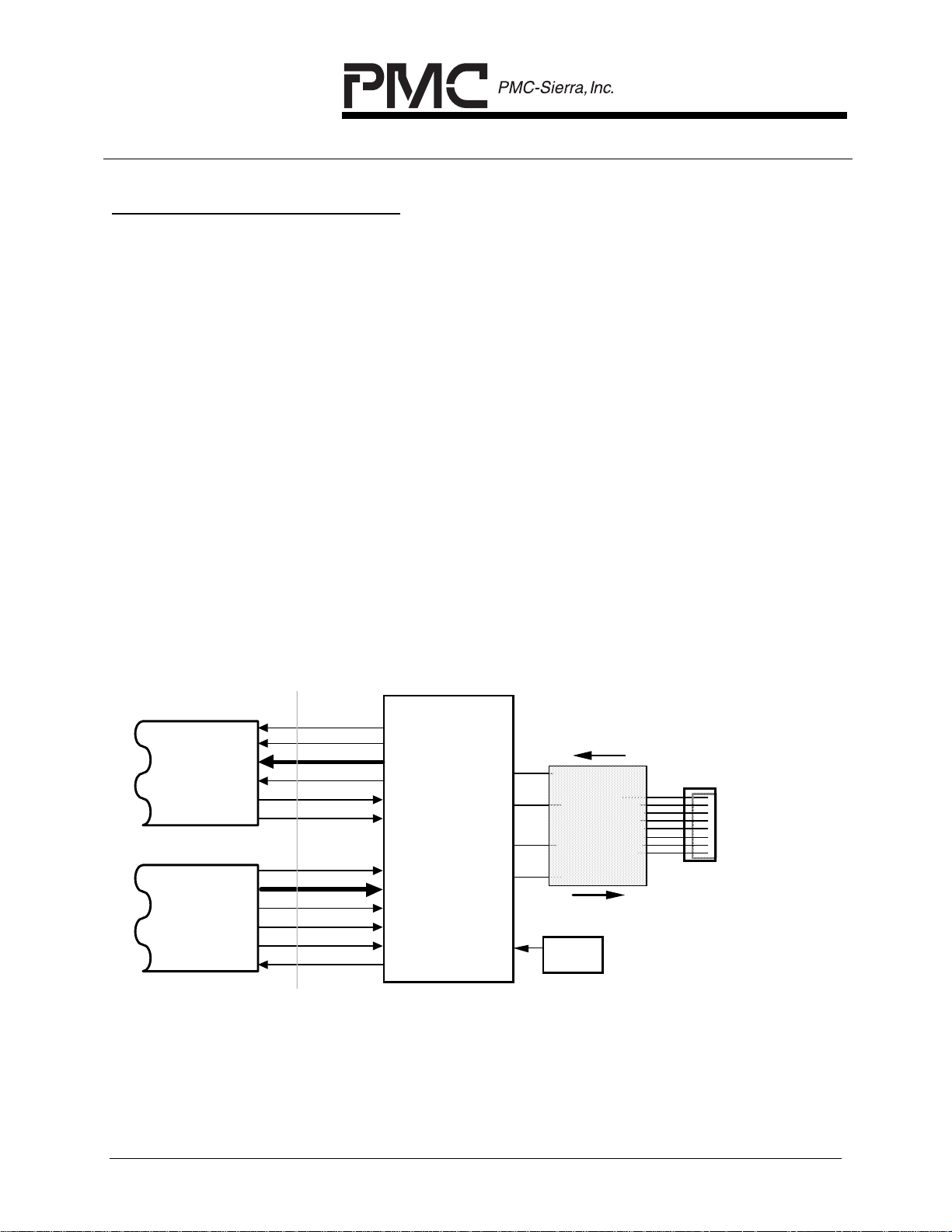
APPLICATION EXAMPLES
The PM5350 S/UNI-ULTRA is typically used to implement the core of an ATM
User Network Interface by which an ATM terminal is linked to an ATM switching
system using SONET/SDH compatible transport.
The S/UNI-ULTRA finds application at either end of terminal to switch links or
switch to switch links, typically in private network (LAN) applications. In this
application, the S/UNI-ULTRA typically interfaces on its line side with line
coupling transformers and baluns.
The S/UNI-ULTRA may be loop timed internally (the recovered clock is used in
the transmit direction) or source timed (separate transmit and receive clocks).
The drop side interfaces directly with ATM adaptation layer or ATM layer
processors. The initial configuration and ongoing control and monitoring of the
S/UNI-ULTRA is provided via a generic microprocessor interface. The S/UNIULTRA also supports a "hardware-only" operating mode where an exter nal
microprocessor is not required. This application is shown in Figure 1.
Figure 1 - Typical ATM Adapter UTP-5 Interface
Receive
AAL
Processor
ATM Terminal
Transmit
AAL
Processor
SCI-PHY
Interface
RXPRTY
RDAT[7:0]
RRDENB
TXPRTY
TDAT[7:0]
TFCLK
TWRENB
RCA
RSOC
RFCLK
TSOC
TCA
RXD+
RXD–
PM5350
S/UNI-155-ULTRA
TXD+
TXD–
REFCLK
Receive
MAGNETICS
Transmit
19.44 MHz
Oscillator
RJ-45
UTP-5 Facilit
PROPRIETARY AND CONFIDENTIAL TO PMC-SIERRA, INC., AND FOR ITS CUSTOMERS’ INTERNAL USE
6
Page 19
PM5350 S/UNI-ULTRA
DATA SHEET
PMC-960924 ISSUE 5 SATURN USER NETWORK INTERFACE
5
BLOCK DIAGRAM
TXD+
TXD-
Analog Edge
RXD+
RXD-
SD
TVREF
Twisted
Pair Tx
Twisted
Pair Rx
TRREF
Clk Gen.
TM
Clk/Data
ATP2
Rec.
REFCLK
Parallel
Serial
Serial
Parallel
Control
to
to
LED
TCLK
TFP
Tx
Framer &
Overhead
Processor
Rx
Framer &
Overhead
Processor
XOFF
TGFC
TCP
Tx ATM
Cell
Processor
Rx ATM
Cell
Processor
Tx ATM
Cell
FIFO
Rx ATM
Cell
FIFO
Microprocessor
I/F
TSOC
TXPRTY
TDAT[7:0]
TCA
TWRENB
TFCLK
RSOC
RXPRTY
RDAT[7:0]
RCA
RRDENB
RFCLK
TSEN
RCAP1
PECLSEL
RCAP2
ATP1
OUT[1:0]
RCLK
RFP
RCP
RGFC
A[7:0]
D[7:0]
ALE
CSB
RDB
WRB
INTB
RSTB
Description
The PM5350 S/UNI-ULTRA Saturn User Network Interface is a monolithic
integrated circuit that implements the SONET/SDH processing and ATM mapping
functions of a 155 Mbit/s or 51Mbit/s ATM User Network Interface. It is fully
compliant with both SONET and SDH requirements and ATM Forum UNI
specifications.
The S/UNI-ULTRA is capable of directly interfacing with UTP-5 cable. At the
receiver end, it performs adaptive equalization. It is fully compliant with the ATM
Forum PMD Interface specifications for 155 Mb/s over twisted pair cable.
The S/UNI-ULTRA receives SONET/SDH frames via a bit serial interface,
recovers clock and data, and processes section, line, and path overhead. It
PROPRIETARY AND CONFIDENTIAL TO PMC-SIERRA, INC., AND FOR ITS CUSTOMERS’ INTERNAL USE
7
Page 20

PM5350 S/UNI-ULTRA
DATA SHEET
PMC-960924 ISSUE 5 SATURN USER NETWORK INTERFACE
performs framing (A1, A2), descrambling, detects alarm conditions, and monitors
section, line, and path bit interleaved parity (B1, B2, B3), accumulating error
counts at each level for performance monitoring purposes. Line and path far end
block error indications (M0 or M1, G1) are also accumulated. The S/UNI-ULTRA
interprets the received payload pointers (H1, H2) and extracts the synchronous
payload envelope which carries the received ATM cell payload.
The S/UNI-ULTRA frames to the ATM payload using cell delineation. HCS error
correction is provided. Idle/unassigned cells may be dropped according to a
programmable filter. Cells are also dropped upon detection of an uncorrectable
header check sequence error. The ATM cell payloads are descrambled. Generic
flow control (GFC) bits from error free cells are extracted and presented on a
serial link for external processing.
Legitimate ATM cells are written to a four cell FIFO buffer. These cells are read
from the FIFO using a synchronous 8 bit wide datapath interface with cell-based
handshake. Counts of received ATM cell headers that are errored and
uncorrectable, those that are errored and correctable and all passed cells are
accumulated independently for performance monitoring purposes.
The S/UNI-ULTRA transmits SONET/SDH frames via a bit serial interface and
formats section, line, and path overhead appropriately. It performs framing
pattern insertion (A1, A2), scrambling, alarm signal insertion, and creates
section, line, and path bit interleaved parity (B1, B2, B3) as required to allow
performance monitoring at the far end. Line and path far end block error
indications (M0 or M1, G1) are also inserted.
The S/UNI-ULTRA generates the payload pointer (H1, H2) and inserts the
synchronous payload envelope which carries the ATM cell payload. It supports
the insertion of a variety of errors into the transmit stream, such as framing
pattern errors, bit interleaved parity errors, and illegal pointers, which are useful
for system diagnostics.
ATM cells are written to an internal programmable-length 4-cell FIFO using a
synchronous 8 bit wide datapath interface. Idle/unassigned cells are
automatically inserted when the internal FIFO contains less than one cell or the
XOFF input is asserted. Generic flow control (GFC) bits may be inserted
downstream of the FIFO via a serial link so that all FIFO latency may be
bypassed. A transmission off (XOFF) input is provided to allow the suspension
of active ATM cell transmission independent of the FIFO fill state.
The S/UNI-ULTRA generates the header check sequence and scrambles the
payload of the ATM cells. Payload scrambling can be disabled.
PROPRIETARY AND CONFIDENTIAL TO PMC-SIERRA, INC., AND FOR ITS CUSTOMERS’ INTERNAL USE
8
Page 21

PM5350 S/UNI-ULTRA
DATA SHEET
PMC-960924 ISSUE 5 SATURN USER NETWORK INTERFACE
No line rate clocks are required directly by the S/UNI-ULTRA as it synthesizes
the transmit clock and recovers the receive clock using a 19.44 MHz reference
clock.
The S/UNI-ULTRA provides output control signals that can be used to command
an LED display, making it easy to visually monitor either alarms, or the transmit
and receive activity.
The S/UNI-ULTRA is configured, controlled and monitored via a generic 8-bit
microprocessor bus interface. It is implemented in low power, +5 Volt CMOS
technology. It has TTL and pseudo-ECL (PECL) compatible inputs and outputs
and is packaged in a 128 pin PQFP package.
PROPRIETARY AND CONFIDENTIAL TO PMC-SIERRA, INC., AND FOR ITS CUSTOMERS’ INTERNAL USE
9
Page 22
PM5350 S/UNI-ULTRA
DATA SHEET
PMC-960924 ISSUE 5 SATURN USER NETWORK INTERFACE
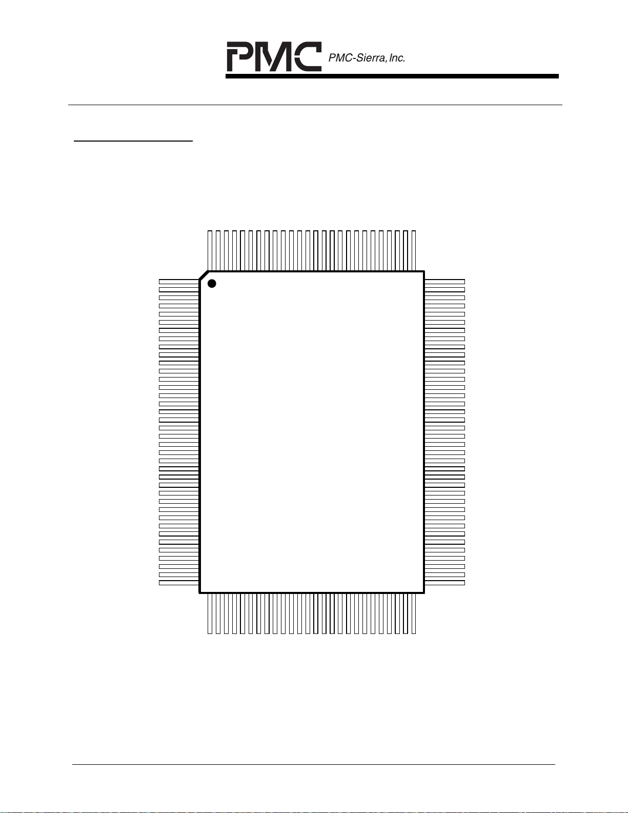
6
PIN DIAGRAM
The S/UNI-ULTRA is packaged in an 128 pin PQFP package having a body size
of 14 mm by 20 mm and a pin pitch of 0.50 mm.
VSSI5
PIN 1
VSS
REFCLK
TAVS2
TAVD2
TAVS1
TAVD1
ATP1
QAVS
QAVD
TAVS3
TAVD3
TXD+
TXD-
TAVD3
TAVS3
TAVD4
TAVS4
TVREF
TRREF
TAVS4
RAVD3
RAVS3
RXD-
RXD+
RAVS3
RAVS3
RCAP1
RCAP2
RAVD3
QAVD
QAVS
ATP2
RAVD1
RAVS1
RAVD2
RAVS2
VSS
PIN 38
PIN 128
.
SD
A[5]
A[6]
A[7]
VSS
Index Pin
A[4]
A[3]
A[2]
A[1]
A[0]
VDDI5
D[7]
D[6]
D[5]
D[4]
VDDO6
VSSO6
D[3]
PM5350
S/UNI-ULTRA
Top
View
D[2]
D[1]
D[0]
INTB
VSSI4
VDDI4
VSS
PIN 103
ALE
PIN 102
VSS
RSTB
CSB
RDB
WRB
TSOC
TXPRTY
TDAT[7]
TDAT[6]
TDAT[5]
TDAT[4]
TDAT[3]
TDAT[2]
TDAT[1]
TDAT[0]
TWRENB
TFCLK
VDDI3
VSSI3
TCA
RSOC
RXPRTY
VDDO5
VSSO5
RDAT[7]
RDAT[6]
RDAT[5]
RDAT[4]
RDAT[3]
RDAT[2]
VDDO4
VSSO4
RDAT[1]
RDAT[0]
RCA
RRDENB
RFCLK
VSS
PIN 65
PIN 39 PIN 64
PROPRIETARY AND CONFIDENTIAL TO PMC-SIERRA, INC., AND FOR ITS CUSTOMERS’ INTERNAL USE
VSS
PECLSEL
OUT[1]
VSSI1
OUT[0]
XOFF
VDDI1
VSSI6
VSSO1
VDDO1
RCP
TCP
TGFC
TCLK
VSSO2
VDDO2
RFP
RCLK
TFP
RGFC
TSEN
VDDI2
VSSI2
VDDO3
VSS
VSSO3
10
Page 23

PM5350 S/UNI-ULTRA
DATA SHEET
PMC-960924 ISSUE 5 SATURN USER NETWORK INTERFACE
7
PIN DESCRIPTION
Pin Name Type Pin
Function
No.
PECLSEL TTL Input 40 The PECL mode select (PECLSEL) is used to
configure the Analog Edge PMD interface for
either PECL or Twisted-pair. A TTL low
configures the interface for while a TTL high
configures the interface for PECL, enabling
direct interfacing with optical transceivers.
Refer to the OPERATION section for a detailed
description of Twisted-Pair mode and PECL
mode configurations. Different termination at
TXD+/- and RXD+/- are required depending on
the selected mode.
RXD+
RXD-
Diff.
Analog
Input
24
23
The differential receiver inputs (RXD+/-) NRZ
data, from the balun/transformer module
interface to these pins when operating in
Twisted-pair mode (as configured via the
PECLSEL pin tied low), or from an optical data
link (ODL) when in PECL mode (as configured
via the PECLSEL pin tied high).
RXD+/- are truly differential inputs offering
superior common-mode noise rejection. Refer
to the APPLICATIONS section of this
document for a description of the required
termination network.
REFCLK TTL Input 2 The reference clock input (REFCLK) must
provide a jitter-free 19.44 MHz reference clock.
It is used as the reference clock by both clock
recovery and clock synthesis circuits.
PROPRIETARY AND CONFIDENTIAL TO PMC-SIERRA, INC., AND FOR ITS CUSTOMERS’ INTERNAL USE
11
Page 24
PM5350 S/UNI-ULTRA
DATA SHEET
PMC-960924 ISSUE 5 SATURN USER NETWORK INTERFACE
Pin Name Type Pin
Function
No.
SD Single-
Ended
PECL
Input
29 The Signal Detect pin (SD) indicates the
presence of valid receive signal power from the
Optical Physical Medium Dependent Device
when operating in PECL mode (as configured
via the PECLSEL pin tied high). A PECL high
indicates the presence of valid data and a
PECL low indicates a loss of signal. It is
mandatory that SD be terminated into the
equivalent network that RXD+/- is terminated
into.
When operated in Twisted-pair mode (as
configured via the PECLSEL pin tied low), SD
has no function and should be connected to
the analog ground common to RAVS3.
RCLK Output 55 The receive clock (RCLK) output provides a
timing reference for the S/UNI-ULTRA receive
outputs. RCLK is a divide by eight of the
recovered line rate clock. RGFC, RCP, RFP
and OUT[1] (when configured for alarm
monitoring) are updated on the rising edge of
RCLK.
PROPRIETARY AND CONFIDENTIAL TO PMC-SIERRA, INC., AND FOR ITS CUSTOMERS’ INTERNAL USE
12
Page 25

PM5350 S/UNI-ULTRA
DATA SHEET
PMC-960924 ISSUE 5 SATURN USER NETWORK INTERFACE
Pin Name Type Pin
No.
OUT[1]
OUT[0]
Output 41
42
Function
The alarm/output por t pins has three functions
as selected by POPC control register bits.
When configured to output alarms, the OUT[1]
output indicates a receive alarm (RALM
function) based on the state of the receive
framer. OUT[1] is low if no receive alarms are
active. OUT[1] is high if an alarm condition is
detected. OUT[1] is updated on the rising
edge of RCLK. In this operation mode OUT[0]
is used as a single bit parallel output port, as
described below.
When configured as a parallel output port,
OUT[1] and OUT[0] can be used to control the
operation of external devices. The signal levels
on the output port are determined by register
bits.
When configured as a traffic indicator port,
OUT[1] indicates the receive traffic activity and
OUT[0] indicates the transmit traffic activity. In
this operation mode OUT[1] and OUT[0]
pulses high fom 100ms on cell receive and
transmit events and can be used to control an
LED display.
RFP Output 56 The receive frame pulse (RFP) output, when
the framing alignment has been found (the
OOF register bit is logic 0), is an 8 kHz signal
derived from the receive line clock. RFP
pulses high for one RCLK cycle every 2430
RCLK cycles for STS-3c (STM-1) rate or every
810 RCLK cycles for STS-1 rate. RFP is
updated on the rising edge of RCLK.
PROPRIETARY AND CONFIDENTIAL TO PMC-SIERRA, INC., AND FOR ITS CUSTOMERS’ INTERNAL USE
13
Page 26

PM5350 S/UNI-ULTRA
DATA SHEET
PMC-960924 ISSUE 5 SATURN USER NETWORK INTERFACE
Pin Name Type Pin
Function
No.
TXD+
TXD-
Diff.
Analog
Output
12
13
The transmit differential data/positive pulse
outputs (TXD+, TXD-) contain NRZ encoded
data. These outputs are open drain current
sinks which interface directly with the Twistedpair network or with an Optical Interface
Module requiring PECL levels.
Refer to the APPLICATIONS section of this
document for a description of the required
termination network.
TFP I/O 58 The active high framing position (TFP) signal is
an 8 kHz timing marker for the transmitter. TFP
defaults to being an input and is used to align
the SONET/SDH transport frame generated by
the S/UNI-ULTRA device to a system
reference. TFP should be brought high for a
single TCLK period every 810 (STS-1) or 2430
(STS-3/STM-1) TCLK cycles, or a multiple
thereof. TFP may be tied low if such
synchronization is not required. TFP is
sampled on the rising edge of TCLK. TFP must
not be used as an input when loop-timed.
When selected as an output through the
interface configuration register, TFP pulses
high for one TCLK cycle every 2430 TCLK
cycles for STS-3c (STM-1) rate or every 810
TCLK cycles for STS-1 rate. TFP is updated
on the rising edge of TCLK.
PROPRIETARY AND CONFIDENTIAL TO PMC-SIERRA, INC., AND FOR ITS CUSTOMERS’ INTERNAL USE
14
Page 27

PM5350 S/UNI-ULTRA
DATA SHEET
PMC-960924 ISSUE 5 SATURN USER NETWORK INTERFACE
Pin Name Type Pin
Function
No.
TSEN Input 59 The tristate enable (TSEN) input selects the
configuration of the receive datapath
(RDAT[7:0], RXPRTY and RSOC). When
TSEN is tied high, RDAT[7:0] operates as a
tristate bus controlled by RRDENB. When
RRDENB is high upon RFCLK rising,
RDAT[7:0], RXPRTY and RSOC are tristated.
When RRDENB is low upon RFCLK rising,
RDAT[7:0], RXPRTY and RSOC are enabled.
When TSEN is tied low, RDAT[7:0], RXPRTY
and RSOC are always enabled, regardless of
the state of RRDENB.
RFCLK Input 66 The receive read clock (RFCLK) is used to
read ATM cells from the receive FIFO. RFCLK
must cycle at a high enough rate to avoid FIFO
overflow. RRDENB is sampled using the rising
edge of RFCLK. RSOC, RDAT[7:0], RXPRTY
and RCA are updated on the rising edge of
RFCLK
RRDENB Input 67 The active low receive read enable input
(RRDENB) is used to initiate reads from the
receive FIFO. When sampled low using the
rising edge of RFCLK, a byte is read from the
internal synchronous FIFO and output on bus
RDAT[7:0] if one is available. When sampled
high using the rising edge of RFCLK, no read
is performed and RDAT[7:0] and RSOC are
tristated if the TSEN input is high. RRDENB
must operate in conjunction with RFCLK to
access the FIFO at a high enough
instantaneous rate as to avoid FIFO overflows.
The ATM layer device may deassert RRDENB
at anytime it is unable to accept another byte.
When the RCA signal is configured to be
deasserted with zero octets (as opposed to
four) in the FIFO, the RCA signal identifies the
valid octets.
PROPRIETARY AND CONFIDENTIAL TO PMC-SIERRA, INC., AND FOR ITS CUSTOMERS’ INTERNAL USE
15
Page 28

PM5350 S/UNI-ULTRA
DATA SHEET
PMC-960924 ISSUE 5 SATURN USER NETWORK INTERFACE
Pin Name Type Pin
No.
RDAT[0]
RDAT[1]
RDAT[2]
RDAT[3]
RDAT[4]
RDAT[5]
RDAT[6]
RDAT[7]
RXPRTY Tristate
Tristate
Output
69
70
73
74
75
76
77
78
81 The receive parity (RXPRTY) signal indicates
Output
Function
The receive cell data (RDAT[7:0]) bus carries
the ATM cell octets that are read from the
receive FIFO. RDAT[7:0] is updated on the
rising edge of RFCLK and is tristated when not
valid if the TSEN input is high. The RDAT[7:0]
bus is always driven when TSEN is low,
regardless of the level of RRDENB.
the parity of the RDAT[7:0] bus. Odd or even
parity selection can be made using a register.
RXPRTY is updated on the rising edge of
RFCLK and is tristated when not valid if the
TSEN input is high. RXPRTY is always driven
when TSEN is low, regardless of the level of
RRDENB.
RSOC Tristate
Output
82 The receive start of cell (RSOC) signal marks
the start of cell on the RDAT[7:0] bus. When
RSOC is high, the first octet of the cell is
present on the RDAT[7:0] stream. RSOC is
updated on the rising edge of RFCLK and is
tristated when not valid if the TSEN input is
high. RSOC is always driven when TSEN is
low, regardless of the level of RRDENB.
RCA Output 68 The receive cell available (RCA) signal
indicates when a cell is available in the receive
FIFO. RCA can be configured to be
deasserted when either zero or four bytes
remain in the FIFO. RCA is updated on the
rising edge of RFCLK. The active polarity of
this signal is programmable and defaults to
active high.
PROPRIETARY AND CONFIDENTIAL TO PMC-SIERRA, INC., AND FOR ITS CUSTOMERS’ INTERNAL USE
16
Page 29

PM5350 S/UNI-ULTRA
DATA SHEET
PMC-960924 ISSUE 5 SATURN USER NETWORK INTERFACE
Pin Name Type Pin
Function
No.
RGFC Output 57 The receive generic flow control (RGFC)
output presents the extracted GFC bits in a
serial stream. The four GFC bits are presented
for each received cell, with the RCP output
indicating the position of the most significant
bit. The updating of RGFC by particular GFC
bits may be disabled through the RACP
Configuration register. The serial link is forced
low if cell delineation is lost. RGFC is updated
on the rising edge of RCLK.
RCP Output 49 The receive cell pulse (RCP) indicates the
location of the four GFC bits in the RGFC
serial stream. RCP is coincident with the most
significant GFC bit. RCP is updated on the
rising edge of RCLK.
TCLK Output 52 The transmit byte clock (TCLK) output provides
a timing reference for S/UNI-ULTRA transmit
outputs. TCLK is a divide by eight of the
synthesized line rate clock. TGFC, TCP and
TFP are sampled on the rising edge of TCLK.
TFCLK Input 86 The transmit write clock (TFCLK) is used to
write ATM cells to the four cell transmit FIFO.
A complete 53 octet cell must be written to the
FIFO before being inserted in the synchronous
payload envelope (SPE). Idle/unassigned cells
are inserted when a complete cell is not
available. TDAT[7:0], TXPRTY, TWRENB and
TSOC are sampled on the rising edge of
TFCLK. TCA is updated on the rising edge of
TFCLK.
PROPRIETARY AND CONFIDENTIAL TO PMC-SIERRA, INC., AND FOR ITS CUSTOMERS’ INTERNAL USE
17
Page 30

PM5350 S/UNI-ULTRA
DATA SHEET
PMC-960924 ISSUE 5 SATURN USER NETWORK INTERFACE
Pin Name Type Pin
Function
No.
TDAT[0]
TDAT[1]
TDAT[2]
TDAT[3]
Input 88
89
90
91
The transmit cell data (TDAT[7:0]) bus carries
the ATM cell octets that are written to the
transmit FIFO. TDAT[7:0] is sampled on the
rising edge of TFCLK and is considered valid
only when TWRENB is simultaneously
asserted.
TDAT[4]
TDAT[5]
TDAT[6]
TDAT[7]
92
93
94
95
TXPRTY Input 96 The transmit parity (TXPRTY) signal indicates
the parity of the TDAT[7:0] bus. Odd or even
parity selection can be made using a register
bit. TXPRTY is sampled on the rising edge of
TFCLK and is considered valid only when
TWRENB is simultaneously asserted.
A parity error is indicated by a status bit and a
maskable interrupt. Cells with parity errors are
not filtered, so the TXPRTY input may be
unused.
TWRENB Input 87 The active low transmit write enable input
(TWRENB) is used to initiate writes to the
transmit FIFO. When sampled low using the
rising edge of TFCLK, the byte on TDAT[7:0] is
written into the transmit FIFO. When sampled
high using the rising edge of TFCLK, no write
is performed. A complete 53 octet cell must be
written to the transmit FIFO before it is
inserted into the SPE. Idle/unassigned cells
are inserted when a complete cell is not
available.
PROPRIETARY AND CONFIDENTIAL TO PMC-SIERRA, INC., AND FOR ITS CUSTOMERS’ INTERNAL USE
18
Page 31

PM5350 S/UNI-ULTRA
DATA SHEET
PMC-960924 ISSUE 5 SATURN USER NETWORK INTERFACE
Pin Name Type Pin
Function
No.
TSOC Input 97 The transmit start of cell (TSOC) signal marks
the start of cell on the TDAT[7:0] bus. When
TSOC is high, the first octet of the cell is
present on the TDAT[7:0] stream. It is not
necessary for TSOC to be present at each cell.
An interrupt may be generated if TSOC is high
during any byte other than the first byte. TSOC
is sampled on the rising edge of TFCLK
TCA Output 83 The transmit cell available (TCA) signal
indicates when a cell is available in the
transmit FIFO. When high, TCA indicates that
the transmit FIFO is not full and a complete
cell may be written in. When TCA goes low, it
indicates either that the transmit FIFO is near
full and can accept no more than four writes or
that the transmit FIFO is full. Selection is
made using a register bit in the TACP FIFO
Control register. To reduce FIFO latency, the
FIFO depth at which TCA indicates "full" can
be set to one, two, three or four cells by the
TACP FIFO Control register. If the
programmed depth is less than four, additional
cells may be written after TCA is deasserted.
TCA is updated on the rising edge of TFCLK.
The active polarity of this signal is
programmable and defaults to active high.
XOFF Input 45 The transmit off (XOFF) input prevents the
insertion of cells from the transmit FIFO. If
XOFF is asserted high, the next cell
transmitted is an idle/unassigned cell
regardless of the number of cells in the FIFO.
Idle/unassigned cells are transmitted until
XOFF is deasserted. XOFF may be treated as
an asynchronous signal.
When the device in set in production test mode
(Master Test Register PMCTST bit set to logic
1) XOFF is used as the test vector clock
(VCLK) signal.
PROPRIETARY AND CONFIDENTIAL TO PMC-SIERRA, INC., AND FOR ITS CUSTOMERS’ INTERNAL USE
19
Page 32

PM5350 S/UNI-ULTRA
DATA SHEET
PMC-960924 ISSUE 5 SATURN USER NETWORK INTERFACE
Pin Name Type Pin
Function
No.
TGFC Input 51 The transmit generic flow control (TGFC) input
provides the ability to insert the GFC value.
The four TCLK periods following the TCP
output pulse contain the GFC value to be
inserted into the current cell. The GFC enable
bits of the TACP Configuration register enable
the insertion of each serial bit. By default, the
GFC values are the contents of the TACP
Idle/Unassigned Cell Header Control register
for idle/unassigned cells and the value
received from TDAT[7:0] for assigned cells.
TGFC is sampled on the rising edge of TCLK.
TCP Output 50 The transmit cell pulse (TCP) indicates where
the valid TGFC serial bits are expected. If TCP
is asserted high, the most significant GFC bit
is expected in the subsequent TCLK period.
TCP pulses high for one TCLK for every
transmitted cell six payload octets before the
first octet of the cell read from the transmit
FIFO, or the idle cell if the FIFO is empty. TCP
is updated on the rising edge of TCLK.
TRREF Analog 19 The reference resistor (TRREF) input is
connected to an off-chip precision resistor
R
to produce calibrated currents for the
REF
TXD+/- outputs. The resistor should be
connected between TRREF and TAVS4.
Please refer to the APPLICATIONS and the
EXTERNAL COMPONENTS sections of this
document for a detailed R
PROPRIETARY AND CONFIDENTIAL TO PMC-SIERRA, INC., AND FOR ITS CUSTOMERS’ INTERNAL USE
specification.
REF
20
Page 33

PM5350 S/UNI-ULTRA
DATA SHEET
PMC-960924 ISSUE 5 SATURN USER NETWORK INTERFACE
Pin Name Type Pin
Function
No.
TVREF Analog 18 The reference voltage (TVREF) is optionally
used to produce calibrated currents for the
TXD +/- outputs. In order to meet tight
amplitude tolerances over process,
temperature and supply, a precise reference
voltage generator V
is required. The other
REF
terminal of the reference generator should be
connected to TAVS4. If this pin is unused, this
input should be connected to analog TAVS4.
Please refer to the APPLICATIONS and the
EXTERNAL COMPONENTS sections of this
RCAP1
RCAP2
ATP1
ATP2
Analog 27
28
Analog 7
33
document for a detailed V
The RCAP1 and RCAP2 pins should be
connected to the RAVS3 analog ground.
Two analog test points (ATP1, ATP2) are
provided for production test purposes. These
pins must be connected to analog ground
specification.
REF
during normal operation.
CSB Input 100 The active low chip select (CSB) signal is low
during S/UNI-ULTRA register accesses. If CSB
is used, it must be held high while RSTB is low
to properly initialize the device. If CSB is not
required (i.e. register accesses are controlled
using the RDB and WRB signals only), CSB
must be connected to an inverted version of
the RSTB input to ensure proper device
initialization. CSB is a Schmitt triggered input
with an integral pull up resistor.
RDB Input 99 The active low read enable (RDB) signal is low
during S/UNI-ULTRA register read accesses.
The S/UNI-ULTRA drives the D[7:0] bus with
the contents of the addressed register while
RDB and CSB are low.
PROPRIETARY AND CONFIDENTIAL TO PMC-SIERRA, INC., AND FOR ITS CUSTOMERS’ INTERNAL USE
21
Page 34

PM5350 S/UNI-ULTRA
DATA SHEET
PMC-960924 ISSUE 5 SATURN USER NETWORK INTERFACE
Pin Name Type Pin
Function
No.
WRB Input 98 The active low write strobe (WRB) signal is low
during a S/UNI-ULTRA register write accesses.
The D[7:0] bus contents are clocked into the
addressed register on the rising WRB edge
while CSB is low.
D[0]
D[1]
D[2]
D[3]
D[4]
D[5]
D[6]
D[7]
A[0]
A[1]
A[2]
I/O 108
109
110
111
114
115
116
117
Input 120
121
122
The bidirectional data bus D[7:0] is used
during S/UNI-ULTRA register read and write
accesses.
The address bus A[7:0] selects specific
registers during S/UNI-ULTRA register
accesses.
A[3]
A[4]
A[5]
A[6]
123
124
125
126
A[7]/TRS 127 The test register select (TRS) signal selects
between normal and test mode register
accesses. TRS is high during test mode
register accesses, and is low during normal
mode register accesses.
RSTB Input 101 The active low reset (RSTB) signal provides an
asynchronous S/UNI-ULTRA reset. RSTB is a
Schmitt triggered input with an integral pull up
resistor.
PROPRIETARY AND CONFIDENTIAL TO PMC-SIERRA, INC., AND FOR ITS CUSTOMERS’ INTERNAL USE
22
Page 35

PM5350 S/UNI-ULTRA
DATA SHEET
PMC-960924 ISSUE 5 SATURN USER NETWORK INTERFACE
Pin Name Type Pin
Function
No.
ALE Input 104 The address latch enable (ALE) is active high
and latches the address bus A[7:0] when low.
When ALE is high, the internal address latches
are transparent. It allows the S/UNI-ULTRA to
interface to a multiplexed address/data bus.
INTB Open-
Drain
Output
107 The active low interrupt (INTB) signal goes low
when a S/UNI-ULTRA interrupt source is
active, and that source is unmasked. The
S/UNI-ULTRA may be enabled to report many
alarms or events via interrupts. INTB returns
high when the interrupt is acknowledged via an
appropriate register access. INTB is an open
drain output and must have an external pull-up
resistor.
VDDI1
VDDI2
VDDI3
Power 44
60
85
The core power (VDDI1 - VDDI5) pins should
be connected to a well decoupled +5 V DC in
common with VDDO.
VDDI4
VDDI5
VSSI1
VSSI2
VSSI3
VSSI4
VSSI5
VSSI6
VDDO1
VDDO2
VDDO3
VDDO4
VDDO5
VDDO6
106
119
Ground 43
61
84
105
118
46
Power 47
53
62
72
80
113
The core ground (VSSI1 - VSSI6) pins should
be connected to GND in common with VSSO.
The pad ring power (VDDO1 - VDDO6) pins
should be connected to a well decoupled +5 V
DC in common with VDDI.
PROPRIETARY AND CONFIDENTIAL TO PMC-SIERRA, INC., AND FOR ITS CUSTOMERS’ INTERNAL USE
23
Page 36

PM5350 S/UNI-ULTRA
DATA SHEET
PMC-960924 ISSUE 5 SATURN USER NETWORK INTERFACE
Pin Name Type Pin
No.
VSSO1
VSSO2
VSSO3
VSSO4
VSSO5
VSSO6
VSS Thermal
Ground 48
54
63
71
79
112
1
Ground
38
39
64
65
102
103
Function
The pad ring ground (VSSO1 - VSSO6) pins
should be connected to GND in common with
VSSI.
The thermal grounds (VSS) provide a low
thermal resistance for the dissipated heat.
These pins are shorted internally and must be
connected to VSSI ground for correct
operation.
TAVD1 Analog
Power
TAVD2 Analog
Power
TAVD3 Analog
Power
TAVD4 Analog
Power
TAVS1 Analog
Ground
128
6 The power (TAVD1) pin for the transmit clock
synthesizer reference circuitry. TAVD1 should
be connected to analog +5V.
4 The power (TAVD2) pin for the transmit clock
synthesizer oscillator. TAVD2 should be
connected to analog +5V.
11
14
The power (TAVD3) pins for the twisted pair
and PECL transmitter output driver. TAVD3
should be connected to analog +5V.
16 The power (TAVD4) pin for the twisted pair and
PECL transmitter block reference circuitry.
TAVD4 should be connected to analog +5V.
5 The ground (TAVS1) pin for the transmit clock
synthesizer reference circuitry. TAVS1 should
be connected to analog GND.
PROPRIETARY AND CONFIDENTIAL TO PMC-SIERRA, INC., AND FOR ITS CUSTOMERS’ INTERNAL USE
24
Page 37

PM5350 S/UNI-ULTRA
DATA SHEET
PMC-960924 ISSUE 5 SATURN USER NETWORK INTERFACE
Pin Name Type Pin
No.
TAVS2 Analog
3 The ground (TAVS2) pin for the transmit clock
Ground
TAVS3 Analog
Ground
TAVS4 Analog
Ground
RAVD1 Analog
10
15
17
20
34 The power (RAVD1) pin for receive clock and
Power
RAVD2 Analog
36 The power (RAVD2) pin for receive clock and
Power
Function
synthesizer oscillator. TAVS2 should be
connected to analog GND.
The ground (TAVS3) pins for the twisted pair
and PECL transmitter output driver. TAVS3
should be connected to analog GND.
The ground (TAVS4) pins for the twisted pair
and PECL transmitter block reference circuitry.
TAVS4 should be connected to analog GND.
data recovery block reference circuitry. RAVD1
should be connected to analog +5V.
data recovery block active loop filter and
oscillator. RAVD2 should be connected to
analog +5V.
RAVD3 Analog
Power
RAVS1 Analog
Ground
RAVS2 Analog
Ground
RAVS3 Analog
Ground
QAVD Analog
Power
QAVS Analog
Ground
21
30
The power (RAVD3) pins for the twisted pair
and PECL receiver block. RAVD3 should be
connected to analog +5V.
35 The ground (RAVS1) pin for receive clock and
data recovery block reference circuitry. RAVS1
should be connected to analog GND.
37 The ground (RAVS2) pin for receive clock and
data recovery block active loop filter and
oscillator. RAVS2 should be connected to
analog GND.
22
25
The ground (RAVS3) pins for the twisted pair
and PECL receiver block. RAVS3 should be
connected to analog GND.
26
9
31
8
32
The power (QAVD) pins for the analog core.
QAVD should be connected to analog +5V.
The ground (QAVS) pins for the analog core.
QAVS should be connected to analog GND.
PROPRIETARY AND CONFIDENTIAL TO PMC-SIERRA, INC., AND FOR ITS CUSTOMERS’ INTERNAL USE
25
Page 38

PM5350 S/UNI-ULTRA
DATA SHEET
PMC-960924 ISSUE 5 SATURN USER NETWORK INTERFACE
Notes on Pin Description:
1. All S/UNI-ULTRA inputs and bidirectionals present minimum capacitive
loading and operate at TTL logic levels except: the SD input operates at
pseudo-ECL (PECL) logic levels; the RXD+ and RXD- inputs can be
configured to operate at either PECL levels or UTP–5 cable interface levels,
respectively.
2. The RDAT[7:0], RXPRTY, RCP, RGFC, RSOC, RCA, TCA, TCP, TCLK and
RCLK outputs have a 4 mA drive capability. All other S/UNI-ULTRA digital
outputs and bidirectionals have 2 mA drive capability. All 4 mA and 2 mA
outputs are slew rate limited. The TXD+ and TXD- outputs have either a 16mA
or 20mA capability, depending if they are configure to operate at PECL or
UTP–5 levels.
3. The VSSO and VSSI ground pins are not internally connected together.
Failure to connect these pins externally may cause malfunction or damage
the device.
4. The VDDO and VDDI power pins are not internally connected together.
Failure to connect these pins externally may cause malfunction or damage
the device.
5. All analog power and ground pins are sensitive to noise. They must be
isolated from the digital power and ground. The TAVD2 and RAVD2 pins
power oscillators; therefore, they generate significant switching noise. Care
must be taken to decouple these pins from each other and all other analog
power and ground pins.
6. The OUT[1] and OUT[0] outputs can control an LED display but must be
buffered to provide a sufficient drive.
7. Due to ESD protection structures in the pads it is necessary to exercise
caution when powering a device up or down. ESD protection devices behave
as diodes between power supply pins and from I/O pins to power supply pins.
Under extreme conditions it is possible to blow these ESD protection devices
or trigger latch up. Please adhere to the recommended power supply
sequencing as described in the OPERATION section of this document.
PROPRIETARY AND CONFIDENTIAL TO PMC-SIERRA, INC., AND FOR ITS CUSTOMERS’ INTERNAL USE
26
Page 39

PM5350 S/UNI-ULTRA
DATA SHEET
PMC-960924 ISSUE 5 SATURN USER NETWORK INTERFACE
FunctionAL Description
7.1 UTP-5 and PECL Receiver
The line receiver (RUTP-5) can be configured to interface with a UTP-5 twisted
pair cable, or to interface with an optical interface module. In the former case it
performs adaptive equalization on the received signal. It is fully compliant to the
ATM Forum PMD Interface specification for 155 Mbit/s over twisted pair cable. In
the latter case, it provides a PECL line interface.
7.2 Clock Recovery
The clock recovery unit recovers the clock from the incoming bit serial data
stream. The clock recovery unit is fully compliant with SONET and SDH jitter
tolerance requirements. The clock recovery unit utilizes a low frequency
reference clock to train and monitor its clock recovery PLL. Under loss of signal
conditions, the clock recovery unit will continue to output a line rate clock that is
locked to this reference for "keep alive" purposes. The clock recovery unit utilizes
a 19.44 MHz reference clock. The clock recovery unit provides status bits that
indicate whether it is locked to data or the reference. The clock recovery unit
also supports diagnostic loopback and a loss of signal input that squelches
normal input data.
Initially, the PLL locks to the reference clock, REFCLK. When the frequency of
the recovered clock is within 488 ppm of the reference clock, the PLL attempts
to lock to the data. Once in data lock, the PLL reverts to the reference clock if no
data transitions occur in 80 bit periods or if the recovered clock drifts beyond 488
ppm of the reference clock.
The internal loop filter transfer function is optimized to enable the PLL to track
the jitter, yet tolerate the minimum transition density expected in a received
SONET data signal. The total loop dynamics of the clock recovery PLL yield a
jitter tolerance which exceeds the minimum tolerance required for SONET
equipment by GR-253-CORE (Figure 2).
PROPRIETARY AND CONFIDENTIAL TO PMC-SIERRA, INC., AND FOR ITS CUSTOMERS’ INTERNAL USE
27
Page 40

PM5350 S/UNI-ULTRA
DATA SHEET
PMC-960924 ISSUE 5 SATURN USER NETWORK INTERFACE
Figure 2 - STS-3c/STM-1Jitter Tolerance
100
10
GR-253-CORE
1
0.1
100 1000 10000 100000 1000000 10000000
Jitter Freq. (Hz )
Note that for frequencies below 300 Hz the jitter tolerance is greater than 15
UIpp; 15 UIpp is the maximum jitter tolerance of the test equipment. If the
recovered clock drifts beyond 488 ppm of the reference, the PLL locks to the
reference clock.
7.3 Serial to Parallel Converter
The Serial to Parallel Converter (SIPO) converts the received bit serial SONET
stream to a byte serial stream. The SIPO searches for the SONET/SDH framing
pattern (A1, A2 ) in the incoming stream, and performs serial to parallel
conversion on octet boundaries.
7.4 Receive Section Overhead Processor
The Receive Section Overhead Processor (RSOP) provides frame
synchronization, descrambling, section level alarm and performance monitoring.
7.4.1 Framer
The Framer Block determines the in-frame/out-of-frame status of the STS-3c or
STS–1 data stream. The loss of frame condition asserts the OUT[1] output with
timing aligned to RCLK (provided POPC receive alarm monitor mode is
selected).
PROPRIETARY AND CONFIDENTIAL TO PMC-SIERRA, INC., AND FOR ITS CUSTOMERS’ INTERNAL USE
28
Page 41

PM5350 S/UNI-ULTRA
DATA SHEET
PMC-960924 ISSUE 5 SATURN USER NETWORK INTERFACE
While in-frame, the framing bytes (A1, A2) in each frame are compared against
the expected pattern. Out-of-frame is declared when four consecutive frames
containing one or more framing pattern errors have been received.
While out-of-frame, the SIPO block monitors the bit serial data stream for an
occurrence of the framing pattern. When a framing pattern has been recognized,
the Framer Block verifies that an error free framing pattern is present in the next
frame before declaring in-frame.
7.4.2 Descramble
The Descramble Block utilizes a frame synchronous descrambler to process the
received byte serial stream. The generating polynomial is 1+x6+x7 and the
sequence length is 127. Details of the descrambling operation are provided in
the references. Note that the framing bytes (A1 and A2) and the section
trace/section growth bytes (J0/Z0) are not descrambled. A register bit is provided
to disable the descrambling operation.
7.4.3 Error Monitor
The Error Monitor Block calculates the received section BIP-8 error detection
code (B1) based on the scrambled data of the complete STS-3c or STS-1 frame.
The section BIP-8 code is based on a bit interleaved parity calculation using
even parity. Details are provided in the references. The calculated BIP-8 code is
compared with the BIP-8 code extracted from the B1 byte of the following frame.
Differences indicate that a section level bit error has occurred. Up to 64000
(8x8000) bit errors can be detected per second. The Error Monitor Block
accumulates these section level bit errors in a 16 bit saturating counter that can
be read via the microprocessor interface. Circuitry is provided to latch this
counter so that its value can be read while simultaneously resetting the internal
counter to 0 or 1, if appropriate, so that a new period of accumulation can begin
without loss of any events. It is intended that this counter be polled at least once
per second so as not to miss bit error events.
7.4.4 Loss of Signal
The Loss of Signal Block monitors the scrambled data of the complete STS–3c
or STS-1 stream for the absence of 1's. When 20±3 µs of all zeros patterns is
detected, a loss of signal (LOS) is declared. Loss of signal is cleared when two
valid framing words are detected and during the intervening time, no loss of
signal condition is detected. The loss of signal condition asserts the RALM
output with timing aligned to RCLK.
PROPRIETARY AND CONFIDENTIAL TO PMC-SIERRA, INC., AND FOR ITS CUSTOMERS’ INTERNAL USE
29
Page 42

PM5350 S/UNI-ULTRA
DATA SHEET
PMC-960924 ISSUE 5 SATURN USER NETWORK INTERFACE
7.4.5 Loss of Frame
The Loss of Frame Block monitors the in-frame / out-of-frame status of the
Framer Block. A loss of frame (LOF) is declared when an out-of-frame (OOF)
condition persists for 3 ms. To provide for intermittent out-of-frame conditions,
the 3 ms timer is not reset to zero until an in-frame condition persists for 3 ms.
The loss of frame is cleared when an in frame condition persists for a period of
3 ms. The loss of frame condition asserts the RALM output with timing aligned to
RCLK.
7.5 Receive Line Overhead Processor
The Receive Line Overhead Processor (RLOP) provides line level alarm and
performance monitoring.
7.5.1 Line Remote Defect Indication Detect
The Line RDI Detect Block detects the presence of Line remote defect indication
(RDI) in the data stream. Line RDI is declared when a 110 binary pattern is
detected in bits 6, 7, and 8 of the K2 byte, for five consecutive frames. Line RDI
is removed when any pattern other than 110 is detected in bits 6, 7, and 8 of the
K2 byte for five consecutive frames. The line RDI status is available through a
maskable interrupt and register bits.
7.5.2 Line AIS Detect
The Line AIS Block detects the presence of a Line Alarm Indication Signal (AIS)
in the data stream. Line AIS is declared when a 111 binary pattern is detected in
bits 6,7,8 of the K2 byte, for five consecutive frames. LAIS is removed when any
pattern other than 111 is detected in bits 6, 7, and 8 of the K2 byte for five
consecutive frames. Line AIS detection asserts the RALM output with timing
aligned to RCLK.
7.5.3 Error Monitor
The Error Monitor Block calculates the received line BIP-8/24 error detection
code (B2) based on the line overhead and synchronous payload envelope of the
data stream. The line BIP-8/24 code is a bit interleaved parity calculation using
even parity. Details are provided in the references. The calculated BIP code is
compared with the BIP-8/24 code extracted from the B3 byte(s) of the following
frame. Any differences indicate that a line layer bit error has occurred. Up to
192000 (24 x 8000) bit errors can be detected per second.
PROPRIETARY AND CONFIDENTIAL TO PMC-SIERRA, INC., AND FOR ITS CUSTOMERS’ INTERNAL USE
30
Page 43

PM5350 S/UNI-ULTRA
DATA SHEET
PMC-960924 ISSUE 5 SATURN USER NETWORK INTERFACE
The Error Monitor Block accumulates these line layer bit errors in a 20 bit
saturating counter that can be read via the microprocessor interface. During a
read, the counter value is latched and the counter is reset to 0 (or 1, if there is an
outstanding event). Note, this counter should be polled at least once per second
to avoid saturation which in turn may result in missed bit error events.
The Error Monitor Block also accumulates line far end block error indications
(contained in the M0/M1 byte) in a similar manner.
7.6 Receive Path Overhead Processor
The Receive Path Overhead Processor (RPOP) provides pointer interpretation,
extraction of path overhead, extraction of the synchronous payload envelope,
and path level alarm and performance monitoring.
7.6.1 Pointer Interpreter
The Pointer Interpreter interprets the incoming pointer (H1, H2) as specified in
the references. The pointer value is used to determine the location of the path
overhead (the J1 byte) in the incoming STS–3c (AU4) or STS–1 (AU3) stream.
The Pointer Interpreter Block detects loss of pointer (LOP) in the incoming STS–
1 or STS–3c. LOP is declared as a result of eight consecutive invalid pointers or
eight consecutive NDF enabled indications. LOP is removed when the same
valid pointer with normal NDF is detected for three consecutive frames.
The Pointer Interpreter Block detects path AIS in the incoming STS–1 or STS–3c
stream. PAIS is declared on entry to the AIS_state after three consecutive AIS
indications. PAIS is removed when the same valid pointer with normal NDF is
detected for three consecutive frames or when a valid with NDF enabled is
detected.
The pointer value is used to extract the path overhead from the incoming stream.
Note that due to anomalies in the standard pointer interpretation rules, certain
illegal pointers may not cause the device to declare a loss of pointer (LOP) state.
In this situation, however, the device will declare a loss of cell delineation state
and return to normal operation when presented with legal pointer values. Such
illegal pointers typically can only be generated continuously by test equipment
and will not normally occur during live-traffic operation.
PROPRIETARY AND CONFIDENTIAL TO PMC-SIERRA, INC., AND FOR ITS CUSTOMERS’ INTERNAL USE
31
Page 44

PM5350 S/UNI-ULTRA
DATA SHEET
PMC-960924 ISSUE 5 SATURN USER NETWORK INTERFACE
7.6.2 Error Monitor
The Error Monitor Block contains two 16-bit counters that are used to accumulate
path BIP-8 errors (B3), and far end block errors (FEBE). The contents of the two
counters may be transferred to holding registers, and the counters reset under
microprocessor control.
Path BIP-8 errors are detected by comparing the path BIP-8 byte (B3) extracted
from the current frame, to the path BIP-8 computed for the previous frame.
FEBEs are detected by extracting the 4-bit FEBE field from the path status byte
(G1). The legal range for the 4-bit field is between 0000 and 1000, representing
zero to eight errors. Any other value is interpreted as zero errors.
Path remote defect indication (RDI) is detected by extracting bit 5 of the path
status byte. Path RDI is declared when bit 5 is set high for five consecutive
frames and is cleared when bit 5 is low for five consecutive frames.
7.7 Receive ATM Cell Processor
The Receive ATM Cell Processor (RACP) performs ATM cell delineation,
provides cell filtering based on idle/unassigned cell detection and HCS error
detection, and performs ATM cell payload descrambling. The RACP also
provides a four cell deep receive FIFO. This FIFO passes a 53 byte data
structure and is used to separate the line timing from the higher layer ATM
system timing.
7.7.1 Cell Delineation
Cell Delineation is the process of framing to ATM cell boundaries using the
header check sequence (HCS) field found in the cell header. The HCS is a
CRC-8 calculation over the first 4 octets of the ATM cell header. When performing
delineation, correct HCS calculations are assumed to indicate cell boundaries.
Cells must be byte aligned before insertion in the synchronous payload
envelope. The cell delineation algorithm searches the 53 possible cell boundary
candidates one at a time to determine the valid cell boundary location. While
searching for the cell boundary location, the cell delineation circuit is in the
HUNT state. When a correct HCS is found, the cell delineation state machine
locks on the particular cell boundary and enters the PRESYNC state. This state
validates the cell boundary location. If the cell boundary is invalid then an
incorrect HCS will be received within the next DELTA cells, at which point a
transition back to the HUNT state is executed. If no HCS errors are detected in
this PRESYNC period then the SYNC state is entered. While in the SYNC state,
PROPRIETARY AND CONFIDENTIAL TO PMC-SIERRA, INC., AND FOR ITS CUSTOMERS’ INTERNAL USE
32
Page 45

PM5350 S/UNI-ULTRA
(by
)
(
(
)
(
DATA SHEET
PMC-960924 ISSUE 5 SATURN USER NETWORK INTERFACE
synchronization is maintained until ALPHA consecutive incorrect HCS patterns
are detected. In such an event a transition is made back to the HUNT state. The
state diagram of the delineation process is shown in Figure 3.
Figure 3 - Cell Delineation State Diagram
correct HCS
te by byte
HUNT
Incorrect HCS
cell by cell
PRESYNC
ALPHA
consecutive
incorrect HCS's
cell by cell)
SYNC
DELTA
consecutive
correct HCS's
cell by cell)
The values of ALPHA and DELTA determine the robustness of the delineation
method. ALPHA determines the robustness against false misalignments due to
bit errors. DELTA determines the robustness against false delineation in the
synchronization process. ALPHA is chosen to be 7 and DELTA is chosen to be 6.
These values result in a maximum average time to delineate of 31 µs for STS–3c
and 93 µs for STS–1.
7.7.2 Descrambler
The self synchronous descrambler operates on the 48 byte cell payload only. The
circuitry descrambles the information field using the 'x43+1' polynomial. The
descrambler is disabled for the duration of the header and HCS fields, and may
optionally be disabled.
PROPRIETARY AND CONFIDENTIAL TO PMC-SIERRA, INC., AND FOR ITS CUSTOMERS’ INTERNAL USE
33
Page 46

PM5350 S/UNI-ULTRA
DATA SHEET
PMC-960924 ISSUE 5 SATURN USER NETWORK INTERFACE
7.7.3 Cell Filter and HCS Verification
Cells are filtered (or dropped) based on HCS errors and/or a cell header pattern.
Cell filtering is optional and is enabled through the RACP registers. Cells are
passed to the receive FIFO while the cell delineation state machine is in the
SYNC state as described above. When both filtering and HCS checking are
enabled, cells are dropped if uncorrectable HCS errors are detected, or if the
corrected header contents match the pattern contained in the 'Match Header
Pattern' and 'Match Header Mask' registers. Idle or unassigned cell filtering is
accomplished by writing the appropriate cell header pattern into the 'Match
Header Pattern' and 'Match Header Mask' registers. Idle/Unassigned cells are
assumed to contain the all zeros pattern in the VCI and VPI fields. The 'Match
Header Pattern' and 'Match Header Mask' registers allow filtering control over the
contents of the GFC, PTI, and CLP fields of the header.
The HCS is a CRC-8 calculation over the first 4 octets of the ATM cell header.
The RACP block verifies the received HCS using the polynomial, x8+x2+x+1.
The coset polynomial, x6+x4+x2+1 is added (modulo 2) to the received HCS
octet before comparison with the calculated result. While the cell delineation
state machine (described above) is in the SYNC state, the HCS verification
circuit implements the state machine shown in Figure 4:
PROPRIETARY AND CONFIDENTIAL TO PMC-SIERRA, INC., AND FOR ITS CUSTOMERS’ INTERNAL USE
34
Page 47

PM5350 S/UNI-ULTRA
DATA SHEET
PMC-960924 ISSUE 5 SATURN USER NETWORK INTERFACE
Figure 4 - HCS Verification State Diagram
ATM DELINEATION
SYNC
STATE
Apparent Multi-Bit Error
(Drop Cell)
ALPHA
consecutive
incorrect HCS's
(To HUNT state)
No Errors
Detected
(Pass Cell)
DELTA
consecutive
correct HCS's
(From PRESYNC
state)
CORRECTION
MODE
No Errors Detected
(Pass Cell)
Single Bit Error
(Correct Error
and Pass Cell)
Errors
Detected
(Drop Cell)
DETECTION
MODE
In normal operation, the HCS verification state machine remains in the
'Correction Mode' state. Incoming cells containing no HCS errors are passed to
the receive FIFO. Incoming single bit errors are corrected, and the resulting cell
is passed to the FIFO. Upon detection of a single bit error or a multi bit error, the
state machine transitions to the 'Detection Mode' state. In this state, the
detection of any HCS error causes the corresponding cell to be dropped. Cells
containing an error-free HCS are passed, and the state machine transitions back
to the 'Correction Mode' state.
7.7.4 Performance Monitor
The Performance Monitor consists of two 8-bit saturating HCS error event
counters and a 19-bit cell counter. One of the counters accumulates correctable
HCS errors (i.e. single HCS bit errors detected while the HCS Verification state
machine is in the 'Correction Mode' state described above). The second counter
accumulates uncorrectable HCS errors (i.e. HCS bit errors detected while the
PROPRIETARY AND CONFIDENTIAL TO PMC-SIERRA, INC., AND FOR ITS CUSTOMERS’ INTERNAL USE
35
Page 48

PM5350 S/UNI-ULTRA
DATA SHEET
PMC-960924 ISSUE 5 SATURN USER NETWORK INTERFACE
HCS Verification state machine is in the 'Detection Mode' state or multiple HCS
bit errors detected while the state machine is in the 'Correction Mode' state as
described above). The cell counter accumulates the number of received
assigned cells. All counters are enabled only when the RACP is in the SYNC
state.
Each counter may be read through the microprocessor interface. Circuitry is
provided to latch these counters so that their values can be read while
simultaneously resetting the internal counters to 0 or 1, if appropriate, so that a
new period of accumulation can begin without loss of any events. It is intended
that the counters be polled at least once per second so HCS error events or cell
counts will not be missed.
7.7.5 GFC Extraction Port
The GFC Extraction Por t outputs the received GFC bits in a serial stream. The
four GFC bits are presented for each received cell, with the RCP output
indicating the position of the most significant bit. The updating of RGFC by
particular GFC bits may be disabled through an internal register. The serial link
is forced low if cell delineation is lost.
7.7.6 Receive FIFO
The Receive FIFO provides FIFO management and a synchronous interface
between the S/UNI-ULTRA device and the external environment. The receive
FIFO can accommodate four cells. The receive FIFO provides for the separation
of the STS-1 or STS-3c line or physical layer timing from the ATM layer timing.
Management functions include filling the receive FIFO, indicating when cells are
available to be read from the receive FIFO, maintaining the receive FIFO read
and write pointers, and detecting FIFO overrun and underrun conditions. Upon
detection of an overrun condition, the FIFO will drop all incoming cells until at
least one cell has been read from the FIFO. At least one cell will be lost during
the FIFO drop operation. Upon detection of an underrun, the offending read is
ignored. FIFO overruns are indicated through a maskable interrupt and register
bit. The interface provided indicates the start of a cell (RSOC) when data is read
from the receive FIFO (using RFCLK) and indicates the cell available status
(RCA). The cell available status may be configured to change from available to
unavailable on read cell boundaries or four reads before the cell boundary.
When the RCA signal is configured to be deasserted with zero octets (as
opposed to four) in the FIFO, it is not an error condition to hold the read enable
(RRDENB) active. In this situation, the RCA signal identifies the valid octets.
PROPRIETARY AND CONFIDENTIAL TO PMC-SIERRA, INC., AND FOR ITS CUSTOMERS’ INTERNAL USE
36
Page 49

PM5350 S/UNI-ULTRA
DATA SHEET
PMC-960924 ISSUE 5 SATURN USER NETWORK INTERFACE
7.8 UTP-5 and PECL Transmitter
The line transmitter (TUTP-5) provides the accurate logic levels required to
interface with a UTP-5 twisted pair, or PECL levels to interface with an optical
interface module. It is fully compliant to the ATM Forum PMD Interface
specification for 155 Mb/s over twisted pair.
7.9 Clock Synthesis
The transmit clock is synthesized from a 19.44 MHz reference. The intrinsic jitter
is minimized when the reference frequency is 19.44 MHz. With a jitter free 19.44
MHz reference input and a low noise board layout, the intrinsic jitter is typically
less than 0.01 UI RMS and 0.10 UI peak-to-peak when measured using a band
pass filter with 12 kHz and 1.3 MHz cutoff frequencies.
7.10 Parallel to Serial Converter
The Parallel to Serial Converter (PISO) converts the internal byte serial stream to
a bit serial stream.
7.11 Transmit Section Overhead Processor
The Transmit Section Overhead Processor (TSOP) provides frame pattern
insertion (A1, A2), scrambling, section level alarm signal insertion, and section
BIP-8 (B1) insertion.
7.11.1 Line AIS Insert
Line AIS insertion results in all bits of the SONET/SDH frame being set to 1
before scrambling except for the section overhead. The Line AIS Insert Block
substitutes all ones as described when enabled through an internal register
accessed through the microprocessor interface. Activation or deactivation of line
AIS insertion is synchronized to frame boundaries.
7.11.2 BIP-8 Insert
The BIP-8 Insert Block calculates and inserts the BIP-8 error detection code (B1)
into the unscrambled data stream.
The BIP–8 calculation is based on the scrambled data of the complete STS–3c
or STS–1 frame. The section BIP–8 code is based on a bit interleaved parity
calculation using even parity. Details are provided in the references. The
PROPRIETARY AND CONFIDENTIAL TO PMC-SIERRA, INC., AND FOR ITS CUSTOMERS’ INTERNAL USE
37
Page 50

PM5350 S/UNI-ULTRA
DATA SHEET
PMC-960924 ISSUE 5 SATURN USER NETWORK INTERFACE
calculated BIP–8 code is then inserted into the B1 byte of the following frame
before scrambling. BIP-8 errors may be continuously inserted under register
control for diagnostic purposes.
7.11.3 Framing and Identity Insert
The Framing and Identity Insert Block inserts the framing bytes (A1, A2) and
identity bytes (C1) into the STS-3c or STS-1 frame. Framing bit errors may be
continuously inserted under register control for diagnostic purposes.
7.11.4 Scrambler
The Scrambler Block utilizes a frame synchronous scrambler to process the
transmit serial stream when enabled through an internal register accessed via
the microprocessor interface. The generating polynomial is 1+x6+x7. Precise
details of the scrambling operation are provided in the references. Note that the
framing bytes and the identity bytes are not scrambled. All zeros may be
continuously inserted (after scrambling) under register control for diagnostic
purposes.
7.12 Transmit Line Overhead Processor
The Transmit Line Overhead Processor (TLOP) provides line level alarm signal
insertion and line BIP-8/24 insertion (B2).
7.12.1 BIP Calculate
The BIP Calculate Block calculates the line BIP error detection code (B2) based
on the line overhead and synchronous payload envelope of the STS-3c or STS-1
stream. The line BIP code is a bit interleaved parity calculation using even parity.
Details are provided in the references. The calculated BIP code is inserted into
the B2 byte positions of the following frame. BIP errors may be continuously
inserted under register control for diagnostic purposes.
7.12.2 Line Remote Defect Indication Insert
The Line RDI Insert Block multiplexes the line overhead bytes into the output
stream and optionally inserts line RDI. Line RDI is inserted by this block when
enabled via register control. Line RDI is inserted by transmitting the code 110
(binary) in bit positions 6, 7, and 8 of the K2 byte contained in the STS–3c or
STS–1 stream.
PROPRIETARY AND CONFIDENTIAL TO PMC-SIERRA, INC., AND FOR ITS CUSTOMERS’ INTERNAL USE
38
Page 51

PM5350 S/UNI-ULTRA
(
)
(
)
(
)
(
)
(
)
(
)
(
)
(
)
(
)
(
)
(
)
(
)
(
)
(*) (
)
(
)
(
)
(
)
(
)
(
)
(
)
(
)
(
)
(
)
(
)
(
)
(
)
(
)
(
)
(
)
(
)
(
)
(
)
(
)
(
)
(
)
(
)
(
)
(
)
(
)
(*)
(*)
(*)
(
)
(
)
(
)
(
)
(
)
(
)
(
)
(
)
(
)
(
)
(
)
(
)
(
)
(
)
(
)
(
)
(
)
(
)
(
)
(
)
(
)
(
)
(
)
(
)
(
)
(
)
(
)
(
)
(
)
(
)
(
)
(
)
(*)
(
)
(
)
(
)
(
)
(
)
DATA SHEET
PMC-960924 ISSUE 5 SATURN USER NETWORK INTERFACE
7.12.3 Line FEBE Insert
The Line FEBE Insert Block accumulates line BIP errors (B2) detected by the
Receive Line Overhead Processor and encodes far end block error indications in
the transmit M0/M1 byte.
Figure 5 - STS-3c/STM-1 Default Transport Overhead Values
A1
0xF6
B1
D1
0x00
H1
0x62
B2
D4
0x00
D7
0x00
D10
0x00
Z1
0x00
A1
0xF6
0x00
0x00
H1
0x93
B2
0x00
0x00
0x00
Z1
0x00
A1
0xF6
0x00
0x00
H1
0x93
B2
0x00
0x00
0x00
Z1
0x00
A2
0x28
E1
0x00
D2
0x00
H2
0x0A
K1
0x00
D5
0x00
D8
0x00
D11
0x00
Z2
0x00
A2
0x28
0x00
0x00
H2
0xFF
0x00
0x00
0x00
0x00
Z2
0x00
A2
0x28
0x00
0x00
H2
0xFF
0x00
0x00
0x00
0x00
M1
J0
0x01
F1
0x00
D3
0x00
H3
0x00
K2
0x00
D6
0x00
D9
0x00
D12
0x00
E2
0x00
Z0
0x02
0x00
0x00
H3
0x00
0x00
0x00
0x00
0x00
0x00
Z0
0x03
0x00
0x00
H3
0x00
0x00
0x00
0x00
0x00
0x00
* : B1, B2 values depend on payload contents
M1 value depends on incoming line bit errors
PROPRIETARY AND CONFIDENTIAL TO PMC-SIERRA, INC., AND FOR ITS CUSTOMERS’ INTERNAL USE
39
Page 52

PM5350 S/UNI-ULTRA
(
)
(
)
(
)
(
)
(*)
(
)
(
)
(
)
(
)
(
)
(
)
(
)
(
)
(*)
(
)
(
)
(
)
(
)
(
)
(
)
(
)
(
)
(
)
(
)
(*)
(
)
(
)
DATA SHEET
PMC-960924 ISSUE 5 SATURN USER NETWORK INTERFACE
Figure 6 - STS-1 Default Transport Overhead Values
A1
0xF6
B1
D1
0x00
H1
0x62
B2
D4
0x00
D7
0x00
D10
0x00
Z1
0x00
A2
0x28
E1
0x00
D2
0x00
H2
0x0A
K1
0x00
D5
0x00
D8
0x00
D11
0x00
M0
J0
0x01
F1
0x00
D3
0x00
H3
0x00
K2
0x00
D6
0x00
D9
0x00
D12
0x00
E2
0x00
* : B1, B2 values depend on payload contents
M0 value depends on incoming line bit errors
7.13 Transmit Path Overhead Processor
The Transmit Path Overhead Processor (TPOP) provides transport frame
alignment generation, pointer generation (H1, H2), path overhead insertion,
insertion of the synchronous payload envelope, inser tion of path level alarm
signals and path BIP-8 (B3) insertion.
7.13.1 Pointer Generator
The Pointer Generator Block generates the outgoing payload pointer (H1, H2).
The block contains a free running time slot counter that locates the start of the
PROPRIETARY AND CONFIDENTIAL TO PMC-SIERRA, INC., AND FOR ITS CUSTOMERS’ INTERNAL USE
40
Page 53

PM5350 S/UNI-ULTRA
DATA SHEET
PMC-960924 ISSUE 5 SATURN USER NETWORK INTERFACE
synchronous payload envelope based on the generated pointer value and the
SONET/SDH frame alignment.
The Pointer Generator Block generates the outgoing pointer as specified in the
references. The concatenation indication (the NDF field set to 1001, I-bits and
D-bits set to all ones, and unused bits set to all zeros) is inserted in the second
and third pointer bytes.
7.13.2 BIP-8 Calculate
The BIP-8 Calculate Block performs a path bit interleaved parity calculation on
the SPE of the outgoing stream. The resulting parity byte is inserted in the path
BIP–8 (B3) byte position of the subsequent frame. BIP–8 errors may be
continuously inserted under register control for diagnostic purposes.
7.13.3 FEBE Calculate
The FEBE Calculate Block accumulates far end block errors on a per frame
basis, and inserts the accumulated value (up to maximum value of eight) in the
FEBE bit positions of the path status (G1) byte. The FEBE information is derived
from path BIP-8 errors detected by the receive path overhead processor, RPOP.
The asynchronous nature of these signals implies that more than eight FEBE
events may be accumulated between transmit G1 bytes. If more than eight
receive Path BIP-8 errors are accumulated between transmit G1 bytes, the
accumulation counter is decremented by eight, and the remaining FEBEs are
transmitted at the next opportunity. Far end block errors may be inserted under
register control for diagnostic purposes.
7.13.4 SPE Multiplexer
The SPE Multiplexer Block multiplexes the payload pointer bytes, the SPE
stream, and the path overhead bytes into the STS–3c or STS–1 stream.
PROPRIETARY AND CONFIDENTIAL TO PMC-SIERRA, INC., AND FOR ITS CUSTOMERS’ INTERNAL USE
41
Page 54

PM5350 S/UNI-ULTRA
(
)
(*)
(
)
(
)
(
)
(
)
(
)
(*)
(*)
DATA SHEET
PMC-960924 ISSUE 5 SATURN USER NETWORK INTERFACE
Figure 7 - Default Path Overhead Values
J1
0x00
B3
C2
0x13
G1
F2
0x00
H4
* : B3 value depend on payload contents
G1 value depends on incoming path bit errors
H4 value depends on cell boundary offset
7.14 Transmit ATM Cell Processor
The Transmit ATM Cell Processor (TACP) inserts H4 framing, provides rate
adaptation via idle/unassigned cell insertion, provides HCS generation and
insertion, and performs ATM cell scrambling. The TACP contains a four cell
transmit FIFO. An idle or unassigned cell is transmitted if a complete ATM cell
has not been written into the FIFO.
Z3
0x00
Z4
0x00
Z5
0x00
PROPRIETARY AND CONFIDENTIAL TO PMC-SIERRA, INC., AND FOR ITS CUSTOMERS’ INTERNAL USE
42
Page 55

PM5350 S/UNI-ULTRA
DATA SHEET
PMC-960924 ISSUE 5 SATURN USER NETWORK INTERFACE
7.14.1 Idle/Unassigned Cell Generator
The Idle/Unassigned Cell Generator inserts idle or unassigned cells into the cell
stream when enabled. Registers are provided to program the GFC, PTI, and
CLP fields of the idle cell header and the idle cell payload. An all zeros pattern is
insert ed into the VCI/VPI bit locations. The idle cell HCS is automatically
calculated and inserted.
7.14.2 Scrambler
The Scrambler scrambles the 48 octet information field. Scrambling is performed
using a parallel implementation of the self synchronous scrambler described in
the references. The cell headers are transmitted unscrambled, and the
scrambler may optionally be completely disabled.
7.14.3 HCS Generator
The HCS Generator performs a CRC-8 calculation over the first four header
octets. A parallel implementation of the polynomial, x8+x2+x+1 is used. The
coset polynomial, x6+x4+x2+1 is added (modulo 2) to the residue. The HCS
Generator inserts the result into the fifth octet of the header.
7.14.4 GFC Insertion Port
The GFC Insertion Port provides the ability to insert the GFC value downstream
of the FIFO. The four GFC bits are received on a serial stream the is
synchronized to the transmit cell by a framing pulse. The GFC enable register
bits control the insertion of each serial bit. If the enable is cleared, the default
GFC value is inserted. For idle/unassigned cells, the default is the contents of
the TACP Idle/Unassigned Cell Header Control register. For assigned cells, the
default is the value received from TDAT[7:0].
7.14.5 Transmit FIFO
The Transmit FIFO provides FIFO management and a synchronous interface
between the S/UNI-ULTRA device and the external environment. The transmit
FIFO can accommodate four cells. It provides for the separation of the physical
layer timing from the ATM layer timing.
Management functions include filling the transmit FIFO, indicating when cells are
available to be written to the transmit FIFO, maintaining the transmit FIFO read
and write pointers, and detecting a FIFO overrun condition. The synchronous
PROPRIETARY AND CONFIDENTIAL TO PMC-SIERRA, INC., AND FOR ITS CUSTOMERS’ INTERNAL USE
43
Page 56

PM5350 S/UNI-ULTRA
DATA SHEET
PMC-960924 ISSUE 5 SATURN USER NETWORK INTERFACE
interface provided to an external device expects the start of a cell (TSOC) when
the first byte of the cell is written to the FIFO (using TFCLK in conjunction with
TWRENB) and indicates the cell available status (TCA). The FIFO status
changes from cell unavailable to cell available on read cell boundaries. The FIFO
status can be configured to change from cell available to cell unavailable on write
cell boundaries or four octets before the end of the cell.
The latency through the transmit FIFO can be controlled by setting the fill level at
which the cell available (TCA) signal is deasserted. Although all four cell buffers
are always accessible, TCA may be programmed to indicate when the FIFO
contains one, two, three or four cells. (The current cell being read out of the
FIFO is included in the count. Be aware that setting a depth of one may limit
throughput.) If a cell write is started immediately after TCA is asserted, the
latency through the device for STS-3c/STM-1 is
latency = depth*(53 line byte periods) + 16 line byte periods (min.)
The latency for STS-1 is
latency = depth*(53 line byte periods) + 10 line byte periods (min.)
The presence of the SONET/SDH overhead accounts for the difference between
the minimum and maximum latencies.
When the FIFO contains four cells and the upstream device writes into the FIFO,
the TACP indicates a FIFO overrun condition using a maskable interrupt and
register bits. The offending write and all subsequent writes are ignored until
there is room in the FIFO.
7.15 Drop Side Interface
7.15.1 Receive Interface
The drop side receive interface can be accessed through a generic 8-bit wide
interface.
= depth*(53 line byte periods) + 26 line byte periods (max.).
= depth*(53 line byte periods) + 14 line byte periods (max.).
External circuitry is notified, using the RCA signal, when a cell is available in the
receive FIFO. External circuitry may then read the cell from the buffer as a byte
wide stream (along with a bit marking the first byte of the cell).
PROPRIETARY AND CONFIDENTIAL TO PMC-SIERRA, INC., AND FOR ITS CUSTOMERS’ INTERNAL USE
44
Page 57

PM5350 S/UNI-ULTRA
DATA SHEET
PMC-960924 ISSUE 5 SATURN USER NETWORK INTERFACE
7.15.2 Transmit Interface
The drop side transmit interface can be accessed through a generic 8-bit wide
interface.
External circuitry is notified, using the TCA signal, when a cell may be written to
the transmit FIFO. The cell is written to the FIFO as a byte wide stream (along
with a bit marking the first byte of the cell).
7.16 Parallel output port and LED display controller
The parallel output port (OUT[1:0]) and LED display controller (POPC) has three
modes of operation: parallel output port, alarm monitor and traffic monitor. The
output port mode provides direct output control, while register bits set the
OUT[1:0] outputs. The output port is either set to a fixed logic value and used to
command an external device, or it toggles at a programmable rate and is used to
command an LED display. The alarm monitor mode allows external monitoring of
alarm conditions through the OUT[1] output (used as RALM). The OUT[1] output
is either set to a static logic value and used to command an external device, or it
toggles at a programmable rate and is used to command an LED display. The
traffic monitor mode provides traffic activity indication and is only intended to
command an external LED display. The controller produces a separate fixed
length 100 ms pulse on OUT[1] when a cell transmit event occurs or on OUT[0]
when a cell receive event occurs.
7.17 Microprocessor Interface
The microprocessor interface block provides normal and test mode registers, and
the logic required to connect to the microprocessor interface. The normal mode
registers are required for normal operation, and test mode registers are used to
enhance the testability of the S/UNI-ULTRA.
The microprocessor interface consist of a bidirectional 8 bit data bus and a
separate 8 bit address bus, which allows both separate address/data bus and
multiplexed address/data bus operations. The interface uses separate read
(RDB) and write (WRB) signals, an address latch enable (ALE), a chip select
(CSB), a master chip reset (RSTB) and the active low interrupt output (INTB).
The register set is accessed as follows:
PROPRIETARY AND CONFIDENTIAL TO PMC-SIERRA, INC., AND FOR ITS CUSTOMERS’ INTERNAL USE
45
Page 58

PM5350 S/UNI-ULTRA
DATA SHEET
PMC-960924 ISSUE 5 SATURN USER NETWORK INTERFACE
8
REGISTER MEMORY MAP
For all register accesses, CSB must be low.
Address Register
0x00 S/UNI-ULTRA Master Reset and Identity / Load Meters
0x01 S/UNI-ULTRA Master Configuration
0x02 S/UNI-ULTRA Master Interrupt Status
0x03 S/UNI-ULTRA Master Mode Control
0x04 S/UNI-ULTRA Master Clock Monitor
0x05 S/UNI-ULTRA Master Control
0x06 S/UNI-ULTRA Clock Synthesis Control and Status
0x07 Reserved
0x08 S/UNI-ULTRA Clock Recovery Control and Status
0x09 S/UNI-ULTRA Clock Recovery Configuration
0x0A S/UNI-ULTRA Transmit Interface Configuration
0x0B Reserved
0x0C S/UNI-ULTRA Receive Interface Configuration
0x0D-0x0F Reserved
0x10 RSOP Control/Interrupt Enable
0x11 RSOP Status/Interrupt Status
0x12 RSOP Section BIP-8 LSB
0x13 RSOP Section BIP-8 MSB
0x14 TSOP Control
0x15 TSOP Diagnostic
0x16-0x17 TSOP Reserved
0x18 RLOP Control/Status
0x19 RLOP Interrupt Enable/Status
0x1A RLOP Line BIP-8/24 LSB
PROPRIETARY AND CONFIDENTIAL TO PMC-SIERRA, INC., AND FOR ITS CUSTOMERS’ INTERNAL USE
46
Page 59

PM5350 S/UNI-ULTRA
DATA SHEET
PMC-960924 ISSUE 5 SATURN USER NETWORK INTERFACE
Address Register
0x1B RLOP Line BIP-8/24
0x1C RLOP Line BIP-8/24 MSB
0x1D RLOP Line FEBE LSB
0x1E RLOP Line FEBE
0x1F RLOP Line FEBE MSB
0x20 TLOP Control
0x21 TLOP Diagnostic
0x22-0x23 TLOP Reserved
0x24-0x2F Reserved
0x30 RPOP Status/Control
0x31 RPOP Interrupt Status
0x32 RPOP Reserved
0x33 RPOP Interrupt Enable
0x34 RPOP Reserved
0x35 RPOP Reserved
0x36 RPOP Reserved
0x37 RPOP Path Signal Label
0x38 RPOP Path BIP-8 LSB
0x39 RPOP Path BIP-8 MSB
0x3A RPOP Path FEBE LSB
0x3B RPOP Path FEBE MSB
0x3C RPOP Reserved
0x3D RPOP Path BIP-8 Configuration
0x3E-0x3F RPOP Reserved
0x40 TPOP Control/Diagnostic
0x41 TPOP Pointer Control
0x42 TPOP Reserved
0x43 TPOP Reserved
PROPRIETARY AND CONFIDENTIAL TO PMC-SIERRA, INC., AND FOR ITS CUSTOMERS’ INTERNAL USE
47
Page 60

PM5350 S/UNI-ULTRA
DATA SHEET
PMC-960924 ISSUE 5 SATURN USER NETWORK INTERFACE
Address Register
0x44 TPOP Reserved
0x45 TPOP Arbitrary Pointer LSB
0x46 TPOP Arbitrary Pointer MSB
0x47 TPOP Reserved
0x48 TPOP Path Signal Label
0x49 TPOP Path Status
0x4A TPOP Reserved
0x4B-0x4F TPOP Reserved
0x50 RACP Control/Status
0x51 RACP Interrupt Enable/Status
0x52 RACP Match Header Pattern
0x53 RACP Match Header Mask
0x54 RACP Correctable HCS Error Count
0x55 RACP Uncorrectable HCS Error Count
0x56 RACP Receive Cell Counter (LSB)
0x57 RACP Receive Cell Counter
0x58 RACP Receive Cell Counter (MSB)
0x59 RACP Configuration
0x5A-0x5F RACP Reserved
0x60 TACP Control/Status
0x61 TACP Idle/Unassigned Cell Header Pattern
0x62 TACP Idle/Unassigned Cell Payload Octet Pattern
0x63 TACP FIFO Configuration
0x64 TACP Transmit Cell Counter (LSB)
0x65 TACP Transmit Cell Counter
0x66 TACP Transmit Cell Counter (MSB)
0x67 TACP Configuration
0x68 POPC Control
PROPRIETARY AND CONFIDENTIAL TO PMC-SIERRA, INC., AND FOR ITS CUSTOMERS’ INTERNAL USE
48
Page 61

PM5350 S/UNI-ULTRA
DATA SHEET
PMC-960924 ISSUE 5 SATURN USER NETWORK INTERFACE
Address Register
0x69 POPC Rate 0
0x6A POPC Rate 1
0x6B POPC Reserved
0x6C-0x7F Reserved
0x80 S/UNI-ULTRA Master Test
0x81-0xFF Reserved for Test
NORMAL MODE REGISTER Description
Normal mode registers are used to configure and monitor the operation of the
S/UNI-ULTRA. Normal mode registers (as opposed to test mode registers) are
selected when TRS (A[7]) is low.
Notes on Normal Mode Register Bits:
1. Writing values into unused register bits has no effect. However, to ensure
software compatibility with future, feature-enhanced versions of the product,
unused register bits must be written with logic zero. Reading back unused
bits can produce either a logic one or a logic zero; hence unused register bits
should be masked off by software when read.
2. All configuration bits that can be written into can also be read back. This
allows the processor controlling the S/UNI-ULTRA to determine the
programming state of the block.
3. Writable normal mode register bits are cleared to logic zero upon reset unless
otherwise noted.
4. Writing into read-only normal mode register bit locations does not affect
S/UNI-ULTRA operation unless otherwise noted.
5. Certain register bits are reserved. These bits are associated with megacell
functions that are unused in this application. To ensure that the S/UNI-ULTRA
operates as intended, reserved register bits must only be written with either
logic zero or logic one, as indicated. Similarly, writing to reserved registers
should be avoided.
PROPRIETARY AND CONFIDENTIAL TO PMC-SIERRA, INC., AND FOR ITS CUSTOMERS’ INTERNAL USE
49
Page 62

PM5350 S/UNI-ULTRA
DATA SHEET
PMC-960924 ISSUE 5 SATURN USER NETWORK INTERFACE
Register 0x00: S/UNI-ULTRA Master Reset and Identity / Load Meters
Bit Type Function Default
Bit 7 R/W RESET 0
Bit 6 R TYPE[2] 1
Bit 5 R TYPE[1] 1
Bit 4 R TYPE[0] 1
Bit 3 R TIP 0
Bit 2 R ID[2] 0
Bit 1 R ID[1] 0
Bit 0 R ID[0] 0
This register allows the revision of the S/UNI-ULTRA to be read by software
permitting graceful migration to support for newer, feature enhanced versions of the
S/UNI-ULTRA. It also provides software reset capability.
Writing to this register (without setting the RESET bit) loads all the error counters in
the RSOP, RLOP, RPOP, RACP and TACP blocks.
ID[2:0]:
The ID bits can be read to provide a binary S/UNI-ULTRA revision number.
TIP:
The TIP bit is set to a logic one when any value with the RESET bit set to
logic 0 is written to this register. Such a write initiates an accumulation
interval transfer and loads all the performance meter registers in the RSOP,
RLOP, RPOP, RACP, and TACP blocks. TIP remains high while the transfer is
in progress, and is set to a logic zero when the transfer is complete. TIP can
be polled by a microprocessor to determine when the accumulation interval
transfer is complete.
TYPE[2:0]:
The TYPE bits distinguish the S/UNI-ULTRA from the other members of the
S/UNI family of devices.
PROPRIETARY AND CONFIDENTIAL TO PMC-SIERRA, INC., AND FOR ITS CUSTOMERS’ INTERNAL USE
50
Page 63

PM5350 S/UNI-ULTRA
DATA SHEET
PMC-960924 ISSUE 5 SATURN USER NETWORK INTERFACE
RESET:
The RESET bit allows the S/UNI-ULTRA to be reset under software control. If
the RESET bit is a logic one, the entire S/UNI-ULTRA is held in reset. This bit
is not self-clearing. Therefore, a logic zero must be written to bring the S/UNIULTRA out of reset. Holding the S/UNI-ULTRA in a reset state places it into a
low power, stand-by mode. A hardware reset clears the RESET bit, thus
negating the software reset. Otherwise the effect of a software reset is
equivalent to that of a hardware reset.
PROPRIETARY AND CONFIDENTIAL TO PMC-SIERRA, INC., AND FOR ITS CUSTOMERS’ INTERNAL USE
51
Page 64

PM5350 S/UNI-ULTRA
DATA SHEET
PMC-960924 ISSUE 5 SATURN USER NETWORK INTERFACE
Register 0x01: S/UNI-ULTRA Master Configuration
Bit Type Function Default
Bit 7 Unused
Bit 6 R/W AUTOFEBE 1
Bit 5 R/W AUTOLRDI 1
Bit 4 R/W AUTOPRDI 1
Bit 3 R/W TCAINV 0
Bit 2 R/W RCAINV 0
Bit 1 R/W Reserved 0
Bit 0 R/W TFP_IN 1
TFP_IN:
The transmit frame pulse interface (TFP_IN) bit determines whether the TFP
pin is used as input or output. If TFP_IN is a logic 0, TFP outputs the transmit
overhead frame pulse for external use. If TFP_IN is a logic 1, TFP is used to
align the SONET/SDH transport frame generated by the S/UNI-ULTRA device
to a system reference.
RCAINV:
The RCAINV bit selects the active polarity of the RCA signal. The default
configuration selects RCA to be active high, indicating that a received cell is
available when high. When RCAINV is set to logic one, the RCA signal
becomes active low.
TCAINV:
The TCAINV bit selects the active polarity of the TCA signal. The default
configuration selects TCA to be active high, indicating that a cell is available
in the transmit FIFO when high. When TCAINV is set to logic one, the TCA
signal becomes active low.
A UTOPRDI
The AUTOPRDI bit determines whether STS path remote defect indication
(RDI) is sent immediately upon detection of an incoming alarm. When
AUTOPRDI is set to logic one, STS path RDI is inserted immediately upon
declaration of loss of signal (LOS), loss of frame (LOF), line AIS, loss of
pointer (LOP) or STS path AIS.
PROPRIETARY AND CONFIDENTIAL TO PMC-SIERRA, INC., AND FOR ITS CUSTOMERS’ INTERNAL USE
52
Page 65

PM5350 S/UNI-ULTRA
DATA SHEET
PMC-960924 ISSUE 5 SATURN USER NETWORK INTERFACE
AUTOLRDI
The AUTOLRDI bit determines whether line remote defect indication (RDI) is
sent immediately upon detection of an incoming alarm. When AUTOLRDI is
set to logic one, line RDI is inserted immediately upon declaration of loss of
signal (LOS), loss of frame (LOF) or line AIS.
AUTOFEBE
The AUTOFEBE bit determines whether line and path far end block errors are
sent upon detection of an incoming line and path BIP error events. When
AUTOFEBE is set to logic one, one line or path FEBE is inserted for each line
or path BIP error event, respectively. When AUTOFEBE is set to logic zero,
incoming line or path BIP error events do not generate FEBE events.
Reserved:
The reserved bits must be programmed to logic zero for proper operation.
PROPRIETARY AND CONFIDENTIAL TO PMC-SIERRA, INC., AND FOR ITS CUSTOMERS’ INTERNAL USE
53
Page 66

PM5350 S/UNI-ULTRA
DATA SHEET
PMC-960924 ISSUE 5 SATURN USER NETWORK INTERFACE
Register 0x02: S/UNI-ULTRA Master Interrupt Status
Bit Type Function Default
Bit 7 R CSUI X
Bit 6 R LCDI X
Bit 5 R CRUI X
Bit 4 R TACPI X
Bit 3 R RACPI X
Bit 2 R RPOPI X
Bit 1 R RLOPI X
Bit 0 R RSOPI X
When the interrupt output INTB goes low, this register allows the source of an active
interrupt to be identified down to the block level. Further register accesses are
required for the block in question to determine the cause of an active interrupt and to
acknowledge the interrupt source.
RSOPI:
The RSOPI bit is high when an interrupt request is active from the RSOP
block. The RSOP interrupt sources are enabled in the RSOP
Control/Interrupt Enable Register.
RLOPI:
The RLOPI bit is high when an interrupt request is active from the RLOP
block. The RLOP interrupt sources are enabled in the RLOP Interrupt
Enable/Status Register.
RPOPI:
The RPOPI bit is high when an interrupt request is active from the RPOP
block. The RPOP interrupt sources are enabled in the RPOP Interrupt Enable
Register.
RACPI:
The RACPI bit is high when an interrupt request is active from the RACP
block. The RACP interrupt sources are enabled in the RACP Interrupt
Enable/Status Register.
PROPRIETARY AND CONFIDENTIAL TO PMC-SIERRA, INC., AND FOR ITS CUSTOMERS’ INTERNAL USE
54
Page 67

PM5350 S/UNI-ULTRA
DATA SHEET
PMC-960924 ISSUE 5 SATURN USER NETWORK INTERFACE
TACPI:
The TACPI bit is high when an interrupt request is active from the TACP block.
The TACP interrupt sources are enabled in the TACP Interrupt Control/Status
Register.
CSUI:
The CSUI bit is high when an interrupt request is active from the Clock
Synthesis Unit. The CSU interrupt sources are enabled in the Clock
Synthesis Interrupt Control/Status Register.
LCDI:
The LCDI interrupt bit is set high when entering and exiting loss of cell
delineation. This bit is reset immediately after a read to this register. The LCD
interrupt is enabled in the S/UNI-ULTRA Master Control Register.
CRUI:
The CRUI bit is high when an interrupt request is active from the Clock
Recovery Unit. The CRU interrupt sources are enabled in the Clock Recovery
Interrupt Control/Status Register.
PROPRIETARY AND CONFIDENTIAL TO PMC-SIERRA, INC., AND FOR ITS CUSTOMERS’ INTERNAL USE
55
Page 68

PM5350 S/UNI-ULTRA
DATA SHEET
PMC-960924 ISSUE 5 SATURN USER NETWORK INTERFACE
Register 0x03: S/UNI-ULTRA Master Mode Control
Bit Type Function Default
Bit 7 Unused X
Bit 6 Unused X
Bit 5 Unused X
Bit 4 Unused X
Bit 3 Unused X
Bit 2 Unused X
Bit 1 R/W RATE[1] 1
Bit 0 R/W RATE[0] 1
RATE[1:0]:
The RATE[1:0] bits select the operation rate of the S/UNI-ULTRA. The default
configuration selects STS-3c rate operation. The S/UNI-ULTRA will not
operate correctly if a Reserved mode is selected.
RATE[1:0] MODE
00 Reserved
01 Reserved
10 51.84 Mbit/s, STS-1
11 155.52 Mbit/s, STS-3c/STM-1
PROPRIETARY AND CONFIDENTIAL TO PMC-SIERRA, INC., AND FOR ITS CUSTOMERS’ INTERNAL USE
56
Page 69

PM5350 S/UNI-ULTRA
DATA SHEET
PMC-960924 ISSUE 5 SATURN USER NETWORK INTERFACE
Register 0x04: S/UNI-ULTRA Master Clock Monitor
Bit Type Function Default
Bit 7 Unused X
Bit 6 Unused X
Bit 5 Unused X
Bit 4 R RFCLKA X
Bit 3 R TFCLKA X
Bit 2 R REFCLKA X
Bit 1 R RCLKA X
Bit 0 R TCLKA X
This register provides activity monitoring on S/UNI-ULTRA clocks. When a
monitored clock signal makes a low to high transition, the corresponding register
bit is set high. The bit will remain high until this register is read, at which point, all
the bits in this register are cleared. A lack of transitions is indicated by the
corresponding register bit reading low. This register should be read at periodic
intervals to detect clock failures.
TCLKA:
The TCLK active (TCLKA) bit monitors for low to high transitions on the TCLK
output. TCLKA is set high on a rising edge of TCLK, and is set low when this
register is read.
RCLKA:
The RCLK active (RCLKA) bit monitors for low to high transitions on the
RCLK output. RCLKA is set high on a rising edge of RCLK, and is set low
when this register is read.
REFCLKA:
The REFCLK active (REFCLKA) bit monitors for low to high transitions on the
REFCLK reference clock input. REFCLKA is set high on a rising edge of
REFCLK, and is set low when this register is read.
PROPRIETARY AND CONFIDENTIAL TO PMC-SIERRA, INC., AND FOR ITS CUSTOMERS’ INTERNAL USE
57
Page 70

PM5350 S/UNI-ULTRA
DATA SHEET
PMC-960924 ISSUE 5 SATURN USER NETWORK INTERFACE
TFCLKA:
The TFCLK active (TFCLKA) bit monitors for low to high transitions on the
TFCLK transmit FIFO clock input. TFCLKA is set high on a rising edge of
TFCLK, and is set low when this register is read.
RFCLKA:
The RFCLK active (RFCLKA) bit monitors for low to high transitions on the
RFCLK receive FIFO clock input. RFCLKA is set high on a rising edge of
RFCLK, and is set low when this register is read.
PROPRIETARY AND CONFIDENTIAL TO PMC-SIERRA, INC., AND FOR ITS CUSTOMERS’ INTERNAL USE
58
Page 71

PM5350 S/UNI-ULTRA
DATA SHEET
PMC-960924 ISSUE 5 SATURN USER NETWORK INTERFACE
Register 0x05: S/UNI-ULTRA Master Control
Bit Type Function Default
Bit 7 R/W LCDE 0
Bit 6 R LCDV X
Bit 5 R/W FIXPTR 1
Bit 4 R/W TPLE 0
Bit 3 R/W PDLE 0
Bit 2 R/W LLE 0
Bit 1 R/W SDLE 0
Bit 0 R/W LOOPT 0
This register controls the timing and high speed loopback features of the S/UNIULTRA.
LOOPT:
The LOOPT bit selects the source of timing for the transmit section of the
S/UNI-ULTRA. When LOOPT is a logic zero, the transmitter timing is derived
from input REFCLK. Only one of the LOOPT, SDLE and LLE bits can be
set to Iogic one at any time.
When LOOPT is a logic one, the transmitter timing is derived from the
receiver inputs RXD+ and RXD- when the CRU is locked on data (RDOOL is
low) and from REFCLK when the CRU is out of data lock (RDOOL is high).
SDLE:
The SDLE bit enables the S/UNI-ULTRA serial diagnostic loopback. When
SDLE is a logic one, the transmit stream is connected to the receive stream.
Only one of the LOOPT, SDLE and LLE bits can be set to Iogic one at
any time.
LLE:
The LLE bit enables the S/UNI-ULTRA line loopback. When LLE is a logic
one, the receive serial data stream is looped back into the transmit serial
stream. This loopback mode includes the RUTP-5, CRU, CSU and TUTP-5
blocks. Only one of the LOOPT, SDLE and LLE bits can be set to Iogic
one at any time.
PROPRIETARY AND CONFIDENTIAL TO PMC-SIERRA, INC., AND FOR ITS CUSTOMERS’ INTERNAL USE
59
Page 72

PM5350 S/UNI-ULTRA
DATA SHEET
PMC-960924 ISSUE 5 SATURN USER NETWORK INTERFACE
PDLE:
The PDLE bit enables the S/UNI-ULTRA parallel diagnostic loopback. When
PDLE is a logic one, the transmit parallel stream is connected to the receive
stream. The loopback point is between the TPOP and the RPOP blocks.
Blocks upstream of the loopback point continue to operate normally. For
example, line AIS may still be inserted in the transmit stream using TSOP.
TPLE:
The TPLE bit enables the S/UNI-ULTRA twisted pair diagnostic loopback.
When TPLE is a logic one, the receive serial data stream is looped back into
the transmit serial stream. This loopback mode includes only the RUTP-5 and
TUTP-5 blocks.
FIXPTR:
The FIXPTR bit disables transmit payload pointer adjustments. If the FIXPTR
bit is a logic 1, the transmit payload pointer is set at 522. If FIXPTR is a logic
zero, the payload pointer is controlled by the contents of the TPOP Pointer
Control register.
LCDV:
The LCDV bit reflects the current loss of cell delineation state. LCDV becomes
a logic 1 when an out of cell delineation state has persisted for 4ms without
any lower level alarms (LOS, LOP, Path AIS, Line AIS) occurring. LCDV
becomes logic 0 when the SYNC state has been maintained for 4ms.
LCDE:
The LCDE bit enables the loss of cell delineation (LCD) interrupt. When logic
one, the S/UNI-ULTRA INTB output is asserted when there is a change in the
LCD state. When logic zero, the S/UNI-ULTRA INTB output is not affected by
the change in LCD state.
PROPRIETARY AND CONFIDENTIAL TO PMC-SIERRA, INC., AND FOR ITS CUSTOMERS’ INTERNAL USE
60
Page 73

PM5350 S/UNI-ULTRA
DATA SHEET
PMC-960924 ISSUE 5 SATURN USER NETWORK INTERFACE
Register 0x06: S/UNI-ULTRA Clock Synthesis Control and Status
Bit Type Function Default
Bit 7 R/W Reserved 0
Bit 6 Unused X
Bit 5 R TROOLI X
Bit 4 Unused X
Bit 3 R TROOLV X
Bit 2 Unused X
Bit 1 R/W TROOLE 0
Bit 0 R/W Reserved 0
This register controls the clock synthesis and reports the state of the transmit
phase locked loop.
TROOLE:
The TROOLE bit is an interrupt enable for the transmit reference out of lock
status. When TROOLE is set to logic one, an interrupt is generated when the
TROOLV bit changes state.
TROOLV:
The transmit reference out of lock status indicates the clock synthesis phase
locked loop is unable to lock to the reference on REFCLK. TROOLV is a logic
one if the divided down synthesized clock frequency not within 488 ppm of
the REFCLK frequency.
TROOLI:
The TROOLI bit is the transmit reference out of lock interrupt status bit.
TROOLI is set high when the TROOLV bit of the S/UNI-ULTRA Clock
Synthesis Control and Status register changes state. TROOLV indicates the
clock synthesis phase locked loop is unable to lock to the reference on
REFCLK and is a logic one if the divided down synthesized clock frequency
not within 488 ppm of the REFCLK frequency. TROOLI is cleared when this
register is read.
Reserved:
The reserved bits must be programmed to logic zero for proper operation.
PROPRIETARY AND CONFIDENTIAL TO PMC-SIERRA, INC., AND FOR ITS CUSTOMERS’ INTERNAL USE
61
Page 74

PM5350 S/UNI-ULTRA
DATA SHEET
PMC-960924 ISSUE 5 SATURN USER NETWORK INTERFACE
Register 0x08: S/UNI-ULTRA Clock Recovery Control and Status
Bit Type Function Default
Bit 7 R/W Reserved 0
Bit 6 R RROOLI X
Bit 5 R RDOOLI X
Bit 4 R RROOLV X
Bit 3 R RDOOLV X
Bit 2 R/W RROOLE 0
Bit 1 R/W RDOOLE 0
Bit 0 R/W Reserved 0
This register controls the clock recovery and reports the state of the receive
phase locked loop.
RDOOLE:
The RDOOLE bit is an interrupt enable for the receive data out of lock status.
When RDOOLE is set to logic one, an interrupt is generated when the
RDOOLV bit changes state.
RROOLE:
The RROOLE bit is an interrupt enable for the reference out of lock status.
When RROOLE is set to logic one, an interrupt is generated when the
RROOLV bit changes state.
RDOOLV:
The receive data out of lock status indicates the clock recovery phase locked
loop is unable to lock to the incoming data stream. RDOOLV is a logic one if
the divided down recovered clock frequency is not within 488 ppm of the
REFCLK frequency or if no transitions have occurred on the RXD+/- inputs for
more than 80 bit periods.
RROOLV:
The receive reference out of lock status indicates the clock recovery phase
locked loop is unable to lock to the receive reference (REFCLK). RROOLV
should be polled after a power up reset to determine when the CRU PLL is
operational. When RROOLV is a logic 1, the CRU is unable to lock to the
PROPRIETARY AND CONFIDENTIAL TO PMC-SIERRA, INC., AND FOR ITS CUSTOMERS’ INTERNAL USE
62
Page 75

PM5350 S/UNI-ULTRA
DATA SHEET
PMC-960924 ISSUE 5 SATURN USER NETWORK INTERFACE
receive reference. When RROOLV is a logic 0, the CRU is locked to the
receive reference. The RROOLV bit may remain set at logic 1 for several
hundred milliseconds after the removal of the power on reset as the CRU PLL
locks to the receive reference clock.
RDOOLI:
The RDOOLI bit is the receive data out of lock interrupt status bit. RDOOLI is
set high when the RDOOLV bit of the S/UNI-ULTRA Clock Recovery Control
and Status register changes state. RDOOLI is cleared when this register is
read.
RROOLI:
The RROOLI bit is the receive reference out of lock interrupt status bit.
RROOLI is set high when the RROOLV bit of the Clock Synthesis Control and
Status register changes state. RROOLI is cleared when this register is read.
Reserved:
The reserved bits must be programmed to logic zero for proper operation.
PROPRIETARY AND CONFIDENTIAL TO PMC-SIERRA, INC., AND FOR ITS CUSTOMERS’ INTERNAL USE
63
Page 76

PM5350 S/UNI-ULTRA
DATA SHEET
PMC-960924 ISSUE 5 SATURN USER NETWORK INTERFACE
Register 0x09: S/UNI-ULTRA Clock Recovery Configuration
Bit Type Function Default
Bit 7 Unused X
Bit 6 Unused X
Bit 5 Unused X
Bit 4 Unused X
Bit 3 Unused X
Bit 2 R/W Reserved 1
Bit 1 R/W Reserved 1
Bit 0 R/W Reserved 1
Reserved:
The reserved bits must be programmed to logic one for proper operation.
PROPRIETARY AND CONFIDENTIAL TO PMC-SIERRA, INC., AND FOR ITS CUSTOMERS’ INTERNAL USE
64
Page 77

PM5350 S/UNI-ULTRA
DATA SHEET
PMC-960924 ISSUE 5 SATURN USER NETWORK INTERFACE
Register 0x0A: S/UNI-ULTRA Line Transmitter Configuration 1
Bit Type Function Default
Bit 7 R/W VREFSEL 0
Bit 6 Unused X
Bit 5 R/W OEN 1
Bit 4 R/W OTQ 0
Bit 3 R/W Reserved 1
Bit 2 R/W Reserved 1
Bit 1 R/W Reserved 0
Bit 0 R/W Reserved 0
This register controls the S/UNI-ULTRA PECL/Twisted-pair transmitter.
OTQ:
The Output True Quiet (OTQ) bit, when set to logic 1, puts the TXD+/- outputs
into a "True Quiet" mode, where the output current is split equally between
the two outputs. When OTQ is set to logic 0 the TXD+/- outputs operate
normally.
OEN:
The output enable (OEN) bit enables the TXD+ and TXD- outputs. When this
signal is set to logic 0, TXD+ and TXD- are high-impedance. When this signal
is set to logic 1, TXD+ and TXD- operate in their normal mode.
VREFSEL:
The voltage reference select (VREFSEL) bit selects which reference voltage
will be used. When VREFSEL is set to logic 0, the internal reference voltage
is selected. When VREFSEL is set to logic 1, the external reference (VREF) is
selected.
Reserved:
The reserved bits must be programmed to logic 0 or logic 1 for proper
operation, as indicated by their default value.
PROPRIETARY AND CONFIDENTIAL TO PMC-SIERRA, INC., AND FOR ITS CUSTOMERS’ INTERNAL USE
65
Page 78

PM5350 S/UNI-ULTRA
DATA SHEET
PMC-960924 ISSUE 5 SATURN USER NETWORK INTERFACE
Register 0x0B: S/UNI-ULTRA Line Transmitter Configuration 2
Bit Type Function Default
Bit 7 R/W Reserved 1
Bit 6 R/W Reserved 1
Bit 5 R/W Reserved 1
Bit 4 R/W Reserved 1
Bit 3 R/W Reserved 1
Bit 2 R/W Reserved 1
Bit 1 R/W Reserved 1
Bit 0 R/W Reserved 1
This register controls the S/UNI-ULTRA PECL/Twisted-pair transmitter.
Reserved:
The reserved bits must be programmed to logic one for proper operation.
PROPRIETARY AND CONFIDENTIAL TO PMC-SIERRA, INC., AND FOR ITS CUSTOMERS’ INTERNAL USE
66
Page 79

PM5350 S/UNI-ULTRA
DATA SHEET
PMC-960924 ISSUE 5 SATURN USER NETWORK INTERFACE
Register 0x0C: S/UNI-ULTRA Line Receiver Configuration
Bit Type Function Default
Bit 7 Unused X
Bit 6 R/W Reserved 0
Bit 5 R/W Reserved 0
Bit 4 R/W Reserved 0
Bit 3 R/W Reserved 0
Bit 2 R/W Reserved 0
Bit 1 R/W Reserved 0
Bit 0 R/W Reserved 1
This register controls the S/UNI-ULTRA PECL/Twisted-pair receiver.
Reserved:
The reserved bits must be programmed to logic 0 or logic 1 for proper
operation, as indicated by their default value.
PROPRIETARY AND CONFIDENTIAL TO PMC-SIERRA, INC., AND FOR ITS CUSTOMERS’ INTERNAL USE
67
Page 80

PM5350 S/UNI-ULTRA
DATA SHEET
PMC-960924 ISSUE 5 SATURN USER NETWORK INTERFACE
Register 0x10: RSOP Control/Interrupt Enable
Bit Type Function Default
Bit 7 R/W Reserved 0
Bit 6 R/W DDS 0
Bit 5 W FOOF X
Bit 4 R/W Reserved 0
Bit 3 R/W BIPEE 0
Bit 2 R/W LOSE 0
Bit 1 R/W LOFE 0
Bit 0 R/W OOFE 0
OOFE:
The OOFE bit is an interrupt enable for the out of frame alarm. When OOFE
is set to logic one, an interrupt is generated when the out of frame alarm
changes state.
LOFE:
The LOFE bit is an interrupt enable for the loss of frame alarm. When LOFE
is set to logic one, an interrupt is generated when the loss of frame alarm
changes state.
LOSE:
The LOSE bit is an interrupt enable for the loss of signal alarm. When LOSE
is set to logic one, an interrupt is generated when the loss of signal alarm
changes state.
BIPEE:
The BIPEE bit is an interrupt enable for the section BIP-8 errors. When
BIPEE is set to logic one, an interrupt is generated when a section BIP-8
error (B1) is detected.
FOOF:
The FOOF bit controls the framing of the RSOP. When a logic one is written
to FOOF, the RSOP is forced out of frame at the next frame boundary. The
FOOF bit is a write only bit, register reads may yield a logic one or a logic
zero.
PROPRIETARY AND CONFIDENTIAL TO PMC-SIERRA, INC., AND FOR ITS CUSTOMERS’ INTERNAL USE
68
Page 81

PM5350 S/UNI-ULTRA
DATA SHEET
PMC-960924 ISSUE 5 SATURN USER NETWORK INTERFACE
DDS:
The DDS bit is set to logic one to disable the descrambling of the STS-3c
(STM-1) or STS-1 stream. When DDS is a logic zero, descrambling is
enabled.
Reserved:
The reserved bits must be programmed to logic zero for proper operation.
PROPRIETARY AND CONFIDENTIAL TO PMC-SIERRA, INC., AND FOR ITS CUSTOMERS’ INTERNAL USE
69
Page 82

PM5350 S/UNI-ULTRA
DATA SHEET
PMC-960924 ISSUE 5 SATURN USER NETWORK INTERFACE
Register 0x11: RSOP Status/Interrupt Status
Bit Type Function Default
Bit 7 Unused X
Bit 6 R BIPEI X
Bit 5 R LOSI X
Bit 4 R LOFI X
Bit 3 R OOFI X
Bit 2 R LOSV X
Bit 1 R LOFV X
Bit 0 R OOFV X
OOFV:
The OOFV bit is read to determine the out of frame state of the RSOP. When
OOFV is high, the RSOP is out of frame. When OOFV is low, the RSOP is
in-frame.
LOFV:
The LOFV bit is read to determine the loss of frame state of the RSOP. When
LOFV is high, the RSOP has declared loss of frame.
LOSV:
The LOSV bit is read to determine the loss of signal state of the RSOP. When
LOSV is high, the RSOP has declared loss of signal.
OOFI:
The OOFI bit is the out of frame interrupt status bit. OOFI is set high when a
change in the out of frame state occurs. This bit is cleared when this register
is read.
LOFI:
The LOFI bit is the loss of frame interrupt status bit. LOFI is set high when a
change in the loss of frame state occurs. This bit is cleared when this register
is read.
PROPRIETARY AND CONFIDENTIAL TO PMC-SIERRA, INC., AND FOR ITS CUSTOMERS’ INTERNAL USE
70
Page 83

PM5350 S/UNI-ULTRA
DATA SHEET
PMC-960924 ISSUE 5 SATURN USER NETWORK INTERFACE
LOSI:
The LOSI bit is the loss of signal interrupt status bit. LOSI is set high when a
change in the loss of signal state occurs. This bit is cleared when this register
is read.
BIPEI:
The BIPEI bit is the section BIP-8 interrupt status bit. BIPEI is set high when
a section layer (B1) bit error is detected. This bit is cleared when this register
is read.
PROPRIETARY AND CONFIDENTIAL TO PMC-SIERRA, INC., AND FOR ITS CUSTOMERS’ INTERNAL USE
71
Page 84

PM5350 S/UNI-ULTRA
DATA SHEET
PMC-960924 ISSUE 5 SATURN USER NETWORK INTERFACE
Register 0x12: RSOP Section BIP-8 LSB
Bit Type Function Default
Bit 7 R SBE[7] X
Bit 6 R SBE[6] X
Bit 5 R SBE[5] X
Bit 4 R SBE[4] X
Bit 3 R SBE[3] X
Bit 2 R SBE[2] X
Bit 1 R SBE[1] X
Bit 0 R SBE[0] X
PROPRIETARY AND CONFIDENTIAL TO PMC-SIERRA, INC., AND FOR ITS CUSTOMERS’ INTERNAL USE
72
Page 85

PM5350 S/UNI-ULTRA
DATA SHEET
PMC-960924 ISSUE 5 SATURN USER NETWORK INTERFACE
Register 0x13: RSOP Section BIP-8 MSB
Bit Type Function Default
Bit 7 R SBE[15] X
Bit 6 R SBE[14] X
Bit 5 R SBE[13] X
Bit 4 R SBE[12] X
Bit 3 R SBE[11] X
Bit 2 R SBE[10] X
Bit 1 R SBE[9] X
Bit 0 R SBE[8] X
SBE[15:0]:
Bits SBE[15:0] represent the number of section BIP-8 errors (B1) that have
been detected since the last time the error count was polled. The error count
is polled by writing to either of the RSOP Section BIP-8 Register addresses.
Such a write transfers the internally accumulated error count to the Section
BIP-8 registers within approximately 7 µs and simultaneously resets the
internal counter to begin a new cycle of error accumulation. This transfer and
reset is carried out in a manner that ensures that coincident events are not
lost.
The error count can also be polled by writing to the S/UNI-ULTRA Master
Reset and Identity / Load Meters register (0x00). Writing to register address
0x00 loads all the error counter registers in the RSOP, RLOP, RPOP and
RACP blocks.
PROPRIETARY AND CONFIDENTIAL TO PMC-SIERRA, INC., AND FOR ITS CUSTOMERS’ INTERNAL USE
73
Page 86

PM5350 S/UNI-ULTRA
DATA SHEET
PMC-960924 ISSUE 5 SATURN USER NETWORK INTERFACE
Register 0x14: TSOP Control
Bit Type Function Default
Bit 7 Unused X
Bit 6 R/W DS 0
Bit 5 R/W Reserved 0
Bit 4 R/W Reserved 0
Bit 3 R/W Reserved 0
Bit 2 R/W Reserved 0
Bit 1 R/W Reserved 0
Bit 0 R/W LAIS 0
LAIS:
The LAIS bit controls the insertion of line alarm indication signal (AIS). When
LAIS is set to logic one, the TSOP inserts AIS into the transmit SONET
stream. Activation or deactivation of line AIS insertion is synchronized to
frame boundaries. Line AIS insertion results in all bits of the SONET frame
being set to 1 prior to scrambling except for the section overhead.
The DC1 bit controls the overwriting of the identity byte(s) in the STS-3c stream.
When DC1 is set low, the identity bytes of the constituent STS-1s in the STS-3c
stream are programmed as specified in the references: STS-1 #1 C1 = 01
hexadecimal, STS-1 #2 C1 = 02 hexadecimal,.., STS-1 #N C1 = N hexadecimal.
When DC1 is set high the PIN[7:0] identity byte positions in each of the
constituent STS-1s are not overwritten.
DS:
The DS bit is set to logic one to disable the scrambling of the STS-3c (STM-1)
or STS–1 stream. When DS is a logic zero, scrambling is enabled.
Reserved:
The reserved bits must be programmed to logic zero for proper operation.
PROPRIETARY AND CONFIDENTIAL TO PMC-SIERRA, INC., AND FOR ITS CUSTOMERS’ INTERNAL USE
74
Page 87

PM5350 S/UNI-ULTRA
DATA SHEET
PMC-960924 ISSUE 5 SATURN USER NETWORK INTERFACE
Register 0x15: TSOP Diagnostic
Bit Type Function Default
Bit 7 Unused X
Bit 6 Unused X
Bit 5 Unused X
Bit 4 Unused X
Bit 3 Unused X
Bit 2 R/W DLOS 0
Bit 1 R/W DBIP8 0
Bit 0 R/W DFP 0
DFP:
The DFP bit controls the insertion of a single bit error continuously in the
most significant bit (bit 1) of the A1 section overhead framing byte. When
DFP is set to logic one, the A1 bytes are set to 0x76 instead of 0xF6.
DBIP8:
The DBIP8 bit controls the insertion of bit errors continuously in the section
BIP-8 byte (B1). When DBIP8 is set to logic one, the B1 byte is inverted.
DLOS:
The DLOS bit controls the insertion of all zeros in the transmit stream. When
DLOS is set to logic one, the transmit stream is forced to 0x00.
PROPRIETARY AND CONFIDENTIAL TO PMC-SIERRA, INC., AND FOR ITS CUSTOMERS’ INTERNAL USE
75
Page 88

PM5350 S/UNI-ULTRA
DATA SHEET
PMC-960924 ISSUE 5 SATURN USER NETWORK INTERFACE
Register 0x18: RLOP Control/Status
Bit Type Function Default
Bit 7 R/W BIPWORD 0
Bit 6 R/W Reserved 0
Bit 5 R/W Reserved 0
Bit 4 R/W Reserved 0
Bit 3 R/W Reserved 0
Bit 2 Unused X
Bit 1 R LAISV 0
Bit 0 R RDIV 0
RDIV:
The RDIV bit is read to determine the remote defect indication state of the
RLOP. When RDIV is high, the RLOP has declared line RDI.
LAISV:
The LAISV bit is read to determine the line AIS state of the RLOP. When
LAISV is high, the RLOP has declared line AIS.
BIPWORD:
The BIPWORD bit controls the accumulation of B2 errors. When BIPWORD
is logic one, the B2 error event counter is incremented only once per frame
whenever one or more B2 bit errors occur during that frame. When BIPWORD
is logic zero, the B2 error event counter is incremented for each B2 bit error
that occurs during that frame (the counter can be incremented up to 8 times
per frame for STS-1 and 24 times per frame for STS-3c).
Reserved:
The reserved bits must be programmed to logic zero for proper operation.
PROPRIETARY AND CONFIDENTIAL TO PMC-SIERRA, INC., AND FOR ITS CUSTOMERS’ INTERNAL USE
76
Page 89

PM5350 S/UNI-ULTRA
DATA SHEET
PMC-960924 ISSUE 5 SATURN USER NETWORK INTERFACE
Register 0x19: RLOP Interrupt Enable/Interrupt Status
Bit Type Function Default
Bit 7 R/W FEBEE 0
Bit 6 R/W BIPEE 0
Bit 5 R/W LAISE 0
Bit 4 R/W RDIE 0
Bit 3 R FEBEI X
Bit 2 R BIPEI X
Bit 1 R LAISI X
Bit 0 R RDII X
RDII:
The RDII bit is the far end receive failure interrupt status bit. RDII is set high
when a change in the line RDI state occurs. This bit is cleared when this
register is read.
LAISI:
The LAISI bit is the line AIS interrupt status bit. LAISI is set high when a
change in the line AIS state occurs. This bit is cleared when this register is
read.
BIPEI:
The BIPEI bit is the line BIP interrupt status bit. BIPEI is set high when a line
layer (B2) bit error is detected. This bit is cleared when this register is read.
FEBEI:
The FEBEI bit is the line far end block error interrupt status bit. FEBEI is set
high when a line layer FEBE (M0/M1) is detected. This bit is cleared when
this register is read.
RDIE:
The RDIE bit is an interrupt enable for the far end receive failure alarm. When
RDIE is set to logic one, an interrupt is generated when RDI changes state.
PROPRIETARY AND CONFIDENTIAL TO PMC-SIERRA, INC., AND FOR ITS CUSTOMERS’ INTERNAL USE
77
Page 90

PM5350 S/UNI-ULTRA
DATA SHEET
PMC-960924 ISSUE 5 SATURN USER NETWORK INTERFACE
LAISE:
The LAISE bit is an interrupt enable for line AIS. When LAISE is set to logic
one, an interrupt is generated when line AIS changes state.
BIPEE:
The BIPEE bit is an interrupt enable for the line BIP-24 errors. When BIPEE
is set to logic one, an interrupt is generated when a line BIP-24 error (B2) is
detected.
FEBEE:
The FEBEE bit is an interrupt enable for the line far end block errors. When
FEBE (M0/M1) is detected.
PROPRIETARY AND CONFIDENTIAL TO PMC-SIERRA, INC., AND FOR ITS CUSTOMERS’ INTERNAL USE
78
Page 91

PM5350 S/UNI-ULTRA
DATA SHEET
PMC-960924 ISSUE 5 SATURN USER NETWORK INTERFACE
Register 0x1A: RLOP Line BIP-8/24 LSB
Bit Type Function Default
Bit 7 R LBE[7] X
Bit 6 R LBE[6] X
Bit 5 R LBE[5] X
Bit 4 R LBE[4] X
Bit 3 R LBE[3] X
Bit 2 R LBE[2] X
Bit 1 R LBE[1] X
Bit 0 R LBE[0] X
PROPRIETARY AND CONFIDENTIAL TO PMC-SIERRA, INC., AND FOR ITS CUSTOMERS’ INTERNAL USE
79
Page 92

PM5350 S/UNI-ULTRA
DATA SHEET
PMC-960924 ISSUE 5 SATURN USER NETWORK INTERFACE
Register 0x1B: RLOP Line BIP-8/24
Bit Type Function Default
Bit 7 R LBE[15] X
Bit 6 R LBE[14] X
Bit 5 R LBE[13] X
Bit 4 R LBE[12] X
Bit 3 R LBE[11] X
Bit 2 R LBE[10] X
Bit 1 R LBE[9] X
Bit 0 R LBE[8] X
PROPRIETARY AND CONFIDENTIAL TO PMC-SIERRA, INC., AND FOR ITS CUSTOMERS’ INTERNAL USE
80
Page 93

PM5350 S/UNI-ULTRA
DATA SHEET
PMC-960924 ISSUE 5 SATURN USER NETWORK INTERFACE
Register 0x1C: RLOP Line BIP-8/24 MSB
Bit Type Function Default
Bit 7 Unused X
Bit 6 Unused X
Bit 5 Unused X
Bit 4 Unused X
Bit 3 R LBE[19] X
Bit 2 R LBE[18] X
Bit 1 R LBE[17] X
Bit 0 R LBE[16] X
LBE[19:0]
Bits LBE[19:0] represent the number of line BIP-8/24 errors (B2) that have
been detected since the last time the error count was polled. The error count
is polled by writing to any of the RLOP Line BIP Register or Line FEBE
Register addresses. Such a write transfers the internally accumulated error
count to the Line BIP Registers within approximately 7 µs and simultaneously
resets the internal counter to begin a new cycle of error accumulation.
The error count can also be polled by writing to the S/UNI-ULTRA Master
Reset and Identity / Load Meters register (0x00). Writing to register address
0x00 loads all the error counter registers in the RSOP, RLOP, RPOP, RACP
and TACP blocks.
PROPRIETARY AND CONFIDENTIAL TO PMC-SIERRA, INC., AND FOR ITS CUSTOMERS’ INTERNAL USE
81
Page 94

PM5350 S/UNI-ULTRA
DATA SHEET
PMC-960924 ISSUE 5 SATURN USER NETWORK INTERFACE
Register 0x1D: RLOP Line FEBE LSB
Bit Type Function Default
Bit 7 R LFE[7] X
Bit 6 R LFE[6] X
Bit 5 R LFE[5] X
Bit 4 R LFE[4] X
Bit 3 R LFE[3] X
Bit 2 R LFE[2] X
Bit 1 R LFE[1] X
Bit 0 R LFE[0] X
PROPRIETARY AND CONFIDENTIAL TO PMC-SIERRA, INC., AND FOR ITS CUSTOMERS’ INTERNAL USE
82
Page 95

PM5350 S/UNI-ULTRA
DATA SHEET
PMC-960924 ISSUE 5 SATURN USER NETWORK INTERFACE
Register 0x1E: RLOP Line FEBE
Bit Type Function Default
Bit 7 R LFE[15] X
Bit 6 R LFE[14] X
Bit 5 R LFE[13] X
Bit 4 R LFE[12] X
Bit 3 R LFE[11] X
Bit 2 R LFE[10] X
Bit 1 R LFE[9] X
Bit 0 R LFE[8] X
PROPRIETARY AND CONFIDENTIAL TO PMC-SIERRA, INC., AND FOR ITS CUSTOMERS’ INTERNAL USE
83
Page 96

PM5350 S/UNI-ULTRA
DATA SHEET
PMC-960924 ISSUE 5 SATURN USER NETWORK INTERFACE
Register 0x1F: RLOP Line FEBE MSB
Bit Type Function Default
Bit 7 Unused X
Bit 6 Unused X
Bit 5 Unused X
Bit 4 Unused X
Bit 3 R LFE[19] X
Bit 2 R LFE[18] X
Bit 1 R LFE[17] X
Bit 0 R LFE[16] X
LFE[19:0]
Bits LFE[19:0] represent the number of line FEBE errors (M0/M1) that have
been detected since the last time the error count was polled. The error count
is polled by writing to any of the RLOP Line BIP Register or Line FEBE
Register addresses. Such a write transfers the internally accumulated error
count to the Line FEBE Registers within approximately 7 µs and
simultaneously resets the internal counter to begin a new cycle of error
accumulation.
The error count can also be polled by writing to the S/UNI-ULTRA Master
Reset and Identity / Load Meters register (0x00). Writing to register address
0x00 loads all the error counter registers in the RSOP, RLOP, RPOP, RACP
and TACP blocks.
PROPRIETARY AND CONFIDENTIAL TO PMC-SIERRA, INC., AND FOR ITS CUSTOMERS’ INTERNAL USE
84
Page 97

PM5350 S/UNI-ULTRA
DATA SHEET
PMC-960924 ISSUE 5 SATURN USER NETWORK INTERFACE
Register 0x20: TLOP Control
Bit Type Function Default
Bit 7 Unused X
Bit 6 R/W Reserved 0
Bit 5 R/W Reserved 0
Bit 4 R/W Reserved 0
Bit 3 R/W Reserved 0
Bit 2 R/W Reserved 0
Bit 1 R/W Reserved 0
Bit 0 R/W RDI 0
RDI:
The RDI bit controls the insertion of line far end receive failure (RDI). When
RDI is set to logic one, the TLOP inserts line RDI into the transmit SONET
stream. Line RDI is inserted by transmitting the code 110 in bit positions 6, 7,
and 8 of the K2 byte of the transmit stream.
Reserved:
The reserved bits must be programmed to logic zero for proper operation.
PROPRIETARY AND CONFIDENTIAL TO PMC-SIERRA, INC., AND FOR ITS CUSTOMERS’ INTERNAL USE
85
Page 98

PM5350 S/UNI-ULTRA
DATA SHEET
PMC-960924 ISSUE 5 SATURN USER NETWORK INTERFACE
Register 0x21: TLOP Diagnostic
Bit Type Function Default
Bit 7 Unused X
Bit 6 Unused X
Bit 5 Unused X
Bit 4 Unused X
Bit 3 Unused X
Bit 2 Unused X
Bit 1 Unused X
Bit 0 R/W DBIP 0
DBIP:
The DBIP bit controls the insertion of bit errors continuously in the line BIP
byte(s) (B2). When DBIP is set to logic one, the B2 byte(s) are inverted.
PROPRIETARY AND CONFIDENTIAL TO PMC-SIERRA, INC., AND FOR ITS CUSTOMERS’ INTERNAL USE
86
Page 99

PM5350 S/UNI-ULTRA
DATA SHEET
PMC-960924 ISSUE 5 SATURN USER NETWORK INTERFACE
Register 0x30: RPOP Status/Control
Bit Type Function Default
Bit 7 R/W Reserved 0
Bit 6 Unused X
Bit 5 R LOP X
Bit 4 Unused X
Bit 3 R PAIS X
Bit 2 R PRDI X
Bit 1 Unused X
Bit 0 R/W Reserved 0
This register allows the status of path level alarms to be monitored.
PRDI, PAIS,LOP:
The PRDI, PAIS, and LOP bits reflect the current state of the corresponding
path level alarms.
Reserved:
The reserved bits must be programmed to logic zero for proper operation.
PROPRIETARY AND CONFIDENTIAL TO PMC-SIERRA, INC., AND FOR ITS CUSTOMERS’ INTERNAL USE
87
Page 100

PM5350 S/UNI-ULTRA
DATA SHEET
PMC-960924 ISSUE 5 SATURN USER NETWORK INTERFACE
Register 0x31: RPOP Interrupt Status
Bit Type Function Default
Bit 7 R PSLI X
Bit 6 Unused X
Bit 5 R LOPI X
Bit 4 Unused X
Bit 3 R PAISI X
Bit 2 R PRDII X
Bit 1 R BIPEI X
Bit 0 R FEBEI X
This register allows identification and acknowledgment of path level alarm and
error event interrupts.
FEBEI, BIPEI:
The BIPEI and FEBEI bits are set to logic one when the corresponding event,
a path BIP-8 error or path FEBE is detected.
PRDII, PAISI, LOPI:
The PRDII, PAISI, and LOPI bits are set to logic one when a transition occurs
in the corresponding alarm state.
PSLI:
The PSLI bit is set to logic one when a change is detected in the path signal
label register. The current path signal label can be read from the RPOP Path
Signal Label register.
These bits (and the interrupt) are cleared when this register is read.
PROPRIETARY AND CONFIDENTIAL TO PMC-SIERRA, INC., AND FOR ITS CUSTOMERS’ INTERNAL USE
88
 Loading...