

Page 1

PM5348 S/UNI-DUAL
DATA SHEET
PMC-950919 ISSUE 7 SATURN USER NETWORK INTERFACE
PM5348
TM
S/
UNI-
155-DUAL
S/UNI-155-DUAL
DUAL SATURN USER NETWORK
INTERFACE 155.52 & 51.84 MBIT/S
DATA SHEET
ISSUE 7: JUNE 1998
PROPRIETARY AND CONFIDENTIAL TO PMC-SIERRA, INC., AND FOR ITS CUSTOMERS’ INTERNAL USE
Page 2
PM5348 S/UNI-DUAL
DATA SHEET
PMC-950919 ISSUE 7 SATURN USER NETWORK INTERFACE
REVISION HISTORY
Issue No. Issue Date Details of Change
7 June 1997 Data Sheet Reformatted — No Change in Technical
Content.
Generated R7 data sheet from PMC-950716, R7
6 Feb 1997 Eng doc P6 revised
PROPRIETARY AND CONFIDENTIAL TO PMC-SIERRA, INC., AND FOR ITS CUSTOMERS’ INTERNAL USE
Page 3

PM5348 S/UNI-DUAL
DATA SHEET
PMC-950919 ISSUE 7 SATURN USER NETWORK INTERFACE
CONTENTS
1 FEATURES...............................................................................................9
2 APPLICATIONS........................................................................................9
3 REFERENCES.........................................................................................9
4 APPLICATION EXAMPLES......................................................................9
5 BLOCK DIAGRAM....................................................................................9
6 DESCRIPTION.........................................................................................9
7 PIN DIAGRAM..........................................................................................9
8 PIN DESCRIPTION..................................................................................9
9 FUNCTIONAL DESCRIPTION.................................................................9
9.1 CLOCK RECOVERY......................................................................9
9.2 SERIAL TO PARALLEL CONVERTER...........................................9
9.3 RECEIVE SECTION OVERHEAD PROCESSOR..........................9
9.3.1 FRAMER.............................................................................9
9.3.2 DESCRAMBLE ...................................................................9
9.3.3 ERROR MONITOR..............................................................9
9.3.4 LOSS OF SIGNAL ..............................................................9
9.3.5 LOSS OF FRAME...............................................................9
9.4 RECEIVE LINE OVERHEAD PROCESSOR .................................9
9.4.1 LINE REMOTE DEFECT INDICATION DETECT ................9
9.4.2 LINE AIS DETECT..............................................................9
9.4.3 AUTOMATIC PROTECTION SWITCH CONTROL BLOCK.9
9.4.4 ERROR MONITOR..............................................................9
PROPRIETARY AND CONFIDENTIAL TO PMC-SIERRA, INC., AND FOR ITS CUSTOMERS’ INTERNAL USE
i
Page 4

PM5348 S/UNI-DUAL
DATA SHEET
PMC-950919 ISSUE 7 SATURN USER NETWORK INTERFACE
9.5 RECEIVE PATH OVERHEAD PROCESSOR.................................9
9.5.1 POINTER INTERPRETER..................................................9
9.5.2 ERROR MONITOR..............................................................9
9.6 RECEIVE ATM CELL PROCESSOR.............................................9
9.6.1 CELL DELINEATION...........................................................9
9.6.2 DESCRAMBLER.................................................................9
9.6.3 CELL FILTER AND HCS VERIFICATION............................9
9.6.4 PERFORMANCE MONITOR...............................................9
9.6.5 RECEIVE FIFO...................................................................9
9.7 CLOCK SYNTHESIS.....................................................................9
9.8 PARALLEL TO SERIAL CONVERTER...........................................9
9.9 TRANSMIT SECTION OVERHEAD PROCESSOR.......................9
9.9.1 LINE AIS INSERT...............................................................9
9.9.2 BIP-8 INSERT.....................................................................9
9.9.3 FRAMING AND SECTION TRACE .....................................9
9.9.4 GENERATION OF TFP .......................................................9
9.9.5 SCRAMBLER......................................................................9
9.10 TRANSMIT LINE OVERHEAD PROCESSOR...............................9
9.10.1APS INSERT.......................................................................9
9.10.2BIP CALCULATE.................................................................9
9.10.3LINE REMOTE DEFECT INDICATION INSERT..................9
9.10.4LINE FEBE INSERT............................................................9
9.11 TRANSMIT PATH OVERHEAD PROCESSOR..............................9
PROPRIETARY AND CONFIDENTIAL TO PMC-SIERRA, INC., AND FOR ITS CUSTOMERS’ INTERNAL USE
ii
Page 5

PM5348 S/UNI-DUAL
DATA SHEET
PMC-950919 ISSUE 7 SATURN USER NETWORK INTERFACE
9.11.1POINTER GENERATOR.....................................................9
9.11.2BIP-8 CALCULATE..............................................................9
9.11.3FEBE CALCULATE.............................................................9
9.11.4SPE MULTIPLEXER............................................................9
9.12 TRANSMIT ATM CELL PROCESSOR...........................................9
9.12.1IDLE/UNASSIGNED CELL GENERATOR...........................9
9.12.2SCRAMBLER......................................................................9
9.12.3HCS GENERATOR..............................................................9
9.12.4TRANSMIT FIFO.................................................................9
9.13 SATURN COMPLIANT SPLIT-BUS PHY INTERFACE (SPHY)......9
9.14 MICROPROCESSOR INTERFACE ...............................................9
10 REGISTER MEMORY MAP......................................................................9
11 NORMAL MODE REGISTER DESCRIPTION..........................................9
12 TEST FEATURES DESCRIPTION ...........................................................9
12.1 TEST MODE 0 DETAILS................................................................9
12.2 JTAG TEST PORT..........................................................................9
13 OPERATION.............................................................................................9
13.1 OVERHEAD BYTE USAGE...........................................................9
13.2 CELL DATA STRUCTURE..............................................................9
13.3 LOOPBACK OPERATION..............................................................9
13.4 BOARD DESIGN RECOMMENDATIONS......................................9
13.5 DRIVING DIFFERENTIAL INPUTS SINGLE ENDED ....................9
13.6 DRIVING THE DIFFERENTIAL REFERENCE CLOCK.................9
PROPRIETARY AND CONFIDENTIAL TO PMC-SIERRA, INC., AND FOR ITS CUSTOMERS’ INTERNAL USE
iii
Page 6

PM5348 S/UNI-DUAL
DATA SHEET
PMC-950919 ISSUE 7 SATURN USER NETWORK INTERFACE
13.7 INTERFACING TO ECL OR PECL DEVICES................................9
13.8 CLOCK RECOVERY......................................................................9
13.9 BIT ERROR RATE MONITOR........................................................9
13.10 JTAG SUPPORT............................................................................9
13.11 POWER SEQUENCING................................................................9
14 FUNCTIONAL TIMING .............................................................................9
14.1 DROP SIDE RECEIVE INTERFACE..............................................9
14.2 DROP SIDE TRANSMIT INTERFACE...........................................9
15 ABSOLUTE MAXIMUM RATINGS............................................................9
16 D.C. CHARACTERISTICS........................................................................9
17 MICROPROCESSOR INTERFACE TIMING CHARACTERISTICS..........9
18 S/UNI-DUAL TIMING CHARACTERISTICS..............................................9
19 ORDERING AND THERMAL INFORMATION ..........................................9
20 MECHANICAL INFORMATION.................................................................9
PROPRIETARY AND CONFIDENTIAL TO PMC-SIERRA, INC., AND FOR ITS CUSTOMERS’ INTERNAL USE
iv
Page 7

PM5348 S/UNI-DUAL
DATA SHEET
PMC-950919 ISSUE 7 SATURN USER NETWORK INTERFACE
LIST OF REGISTERS
REGISTER 0X000: S/UNI-DUAL MASTER RESET AND IDENTITY / CHANNEL
#1 MONITORING UPDATE.......................................................................9
REGISTER 0X080: S/UNI-DUAL CHANNEL #2 MONITORING UPDATE...........9
REGISTER 0X001, 0X081: S/UNI-DUAL CONFIGURATION..............................9
REGISTER 0X002, 0X082: S/UNI-DUAL INTERRUPT STATUS.........................9
REGISTER 0X003: S/UNI-DUAL MASTER MODE CONTROL...........................9
REGISTER 0X004: S/UNI-DUAL MASTER CLOCK MONITOR..........................9
REGISTER 0X005, 0X085: S/UNI-DUAL CONTROL..........................................9
REGISTER 0X006: S/UNI-DUAL CLOCK SYNTHESIS CONTROL AND STATUS
..................................................................................................................9
REGISTER 0X007, 0X087: S/UNI-DUAL CLOCK RECOVERY CONTROL AND
STATUS ....................................................................................................9
REGISTER 0X008: S/UNI-DUAL INTERFACE CONTROL .................................9
REGISTER 0X009: S/UNI-DUAL OUTPUT PORT CONTROL............................9
REGISTER 0X00A: S/UNI-DUAL POP[0] STROBE RATE..................................9
REGISTER 0X00B: S/UNI-DUAL POP[1] STROBE RATE..................................9
REGISTER 0X00C: S/UNI-DUAL POP[2] STROBE RATE..................................9
REGISTER 0X00D: S/UNI-DUAL POP[3] STROBE RATE..................................9
REGISTER 0X00E, 0X08E: TRANSMIT SYNCHRONIZATION STATUS ............9
REGISTER 0X010, 0X090: RSOP CONTROL/INTERRUPT ENABLE ...............9
REGISTER 0X011, 0X091: RSOP STATUS/INTERRUPT STATUS.....................9
REGISTER 0X012, 0X092: RSOP SECTION BIP-8 LSB....................................9
REGISTER 0X013, 0X093: RSOP SECTION BIP-8 MSB...................................9
PROPRIETARY AND CONFIDENTIAL TO PMC-SIERRA, INC., AND FOR ITS CUSTOMERS’ INTERNAL USE
v
Page 8

PM5348 S/UNI-DUAL
DATA SHEET
PMC-950919 ISSUE 7 SATURN USER NETWORK INTERFACE
REGISTER 0X014, 0X094: TSOP CONTROL ....................................................9
REGISTER 0X015, 0X095: TSOP DIAGNOSTIC................................................9
REGISTER 0X018, 0X098: RLOP CONTROL/STATUS......................................9
REGISTER 0X019, 0X099: RLOP INTERRUPT ENABLE/INTERRUPT STATUS9
REGISTER 0X01A, 0X09A: RLOP LINE BIP-8/24 LSB......................................9
REGISTER 0X01B, 0X09B: RLOP LINE BIP-8/24..............................................9
REGISTER 0X01C, 0X09C: RLOP LINE BIP-8/24 MSB.....................................9
REGISTER 0X01D, 0X09D: RLOP LINE FEBE LSB...........................................9
REGISTER 0X01E, 0X09E: RLOP LINE FEBE...................................................9
REGISTER 0X01F, 0X09F: RLOP LINE FEBE MSB...........................................9
REGISTER 0X020, 0X0A0: TLOP CONTROL ....................................................9
REGISTER 0X021, 0X0A1: TLOP DIAGNOSTIC................................................9
REGISTER 0X022, 0X0A2: TLOP TRANSMIT K1 ..............................................9
REGISTER 0X023, 0X0A3: TLOP TRANSMIT K2 ..............................................9
REGISTER 0X030, 0X0B0: RPOP STATUS/CONTROL .....................................9
REGISTER 0X031, 0X0B1: RPOP INTERRUPT STATUS ..................................9
REGISTER 0X033, 0X0B3: RPOP INTERRUPT ENABLE.................................9
REGISTER 0X037, 0X0B7: RPOP PATH SIGNAL LABEL..................................9
REGISTER 0X038, 0X0B8: RPOP PATH BIP-8 LSB...........................................9
REGISTER 0X039, 0X0B9: RPOP PATH BIP-8 MSB..........................................9
REGISTER 0X03A, 0X0BA: RPOP PATH FEBE LSB .........................................9
REGISTER 0X03B, 0X0BB: RPOP PATH FEBE MSB ........................................9
REGISTER 0X03D, 0X0BD: RPOP PATH BIP-8 CONFIGURATION...................9
PROPRIETARY AND CONFIDENTIAL TO PMC-SIERRA, INC., AND FOR ITS CUSTOMERS’ INTERNAL USE
vi
Page 9

PM5348 S/UNI-DUAL
DATA SHEET
PMC-950919 ISSUE 7 SATURN USER NETWORK INTERFACE
REGISTER 0X040, 0X0C0: TPOP CONTROL/DIAGNOSTIC.............................9
REGISTER 0X041, 0X0C1: TPOP POINTER CONTROL...................................9
REGISTER 0X045, 0X0C5: TPOP ARBITRARY POINTER LSB ........................9
REGISTER 0X046, 0X0C6: TPOP ARBITRARY POINTER MSB .......................9
REGISTER 0X048, 0X0C8: TPOP PATH SIGNAL LABEL ..................................9
REGISTER 0X049, 0X0C9: TPOP PATH STATUS...............................................9
REGISTER 0X050, 0X0D0: RACP CONTROL/STATUS .....................................9
REGISTER 0X051, 0X0D1: RACP INTERRUPT ENABLE/STATUS ...................9
REGISTER 0X052, 0X0D2: RACP MATCH HEADER PATTERN........................9
REGISTER 0X053, 0X0D3: RACP MATCH HEADER MASK..............................9
REGISTER 0X054, 0X0D4: RACP CORRECTABLE HCS ERROR COUNT.......9
REGISTER 0X055, 0X0D5: RACP UNCORRECTABLE HCS ERROR COUNT .9
REGISTER 0X056, 0X0D6: RACP RECEIVE CELL COUNTER (LSB)...............9
REGISTER 0X057, 0X0D7: RACP RECEIVE CELL COUNTER.........................9
REGISTER 0X058, 0X0D8: RACP RECEIVE CELL COUNTER (MSB)..............9
REGISTER 0X059, 0X0D9: RACP CONFIGURATION........................................9
REGISTER 0X060, 0X0E0: TACP CONTROL/STATUS.......................................9
REGISTER 0X061, 0X0E1: TACP IDLE/UNASSIGNED CELL HEADER
PATTERN..................................................................................................9
REGISTER 0X062, 0X0E2: TACP IDLE/UNASSIGNED CELL PAYLOAD OCTET
PATTERN..................................................................................................9
REGISTER 0X063, 0X0E3: TACP FIFO CONTROL............................................9
REGISTER 0X064, 0X0E4: TACP TRANSMIT CELL COUNTER (LSB) .............9
REGISTER 0X065, 0X0E5: TACP TRANSMIT CELL COUNTER........................9
PROPRIETARY AND CONFIDENTIAL TO PMC-SIERRA, INC., AND FOR ITS CUSTOMERS’ INTERNAL USE
vii
Page 10

PM5348 S/UNI-DUAL
DATA SHEET
PMC-950919 ISSUE 7 SATURN USER NETWORK INTERFACE
REGISTER 0X066, 0X0E6: TACP TRANSMIT CELL COUNTER (MSB).............9
REGISTER 0X067, 0X0E7: TACP CONFIGURATION.........................................9
REGISTERS 0X068, 0X0E8: RASE INTERRUPT ENABLE...............................9
REGISTERS 0X069, 0X0E9: RASE INTERRUPT STATUS ................................9
REGISTERS 0X06A, 0X0EA: RASE CONFIGURATION/CONTROL REGISTER9
REGISTERS 0X06B, 0X0EB: RASE SF ACCUMULATION PERIOD (LSB)........9
REGISTERS 0X06C, 0X0EC: RASE SF ACCUMULATION PERIOD..................9
REGISTERS 0X06D, 0X0ED: RASE SF ACCUMULATION PERIOD (MSB).......9
REGISTERS 0X06E, 0X0EE: RASE SF SATURATION THRESHOLD (LSB) .....9
REGISTERS 0X06F, 0X0EF: RASE SF SATURATION THRESHOLD (MSB)......9
REGISTERS 0X070, 0X0F0: RASE SF DECLARING THRESHOLD (LSB)........9
REGISTERS 0X071, 0X0F1: RASE SF DECLARING THRESHOLD (MSB).......9
REGISTERS 0X072, 0X0F2: RASE SF CLEARING THRESHOLD (LSB)..........9
REGISTERS 0X073, 0X0F3: RASE SF CLEARING THRESHOLD (MSB).........9
REGISTERS 0X07D, 0X0FD: RASE RECEIVE K1.............................................9
REGISTERS 0X07E, 0X0FE: RASE RECEIVE K2.............................................9
REGISTERS 0X07F, 0X0FF: RASE RECEIVE S1..............................................9
REGISTER 0X100: MASTER TEST....................................................................9
PROPRIETARY AND CONFIDENTIAL TO PMC-SIERRA, INC., AND FOR ITS CUSTOMERS’ INTERNAL USE
viii
Page 11

PM5348 S/UNI-DUAL
DATA SHEET
PMC-950919 ISSUE 7 SATURN USER NETWORK INTERFACE
LIST OF FIGURES
FIGURE 1 - SPLIT-BUS 8-BIT DIRECT-PHY ATM SWITCH INTERFACE .........9
FIGURE 2 - DIRECT 8-BIT OR 16-BIT MULTI-PHY ATM SWITCH INTERFACE9
FIGURE 3 - STS-3C/STM-1JITTER TOLERANCE ............................................9
FIGURE 4 - CELL DELINEATION STATE DIAGRAM.........................................9
FIGURE 5 - HCS VERIFICATION STATE DIAGRAM ......................................... 9
FIGURE 6 - STS-3C/STM-1 DEFAULT TRANSPORT OVERHEAD VALUES ....9
FIGURE 7 - STS-1 DEFAULT TRANSPORT OVERHEAD VALUES...................9
FIGURE 8 - DEFAULT PATH OVERHEAD VALUES...........................................9
FIGURE 9 - STS-3C (STM-1) OVERHEAD........................................................9
FIGURE 10- STS-1 OVERHEAD ........................................................................9
FIGURE 11- 16-BIT WIDE, 27 WORD STRUCTURE..........................................9
FIGURE 12- 8-BIT WIDE, 53 WORD STRUCTURE............................................9
FIGURE 13- LINE LOOPBACK MODE...............................................................9
FIGURE 14- SERIAL DIAGNOSTIC LOOPBACK MODE...................................9
FIGURE 15- PARALLEL DIAGNOSTIC LOOPBACK MODE..............................9
FIGURE 16- SINGLE ENDED DRIVING DIFFERENTIAL INPUTS....................9
FIGURE 17- DRIVING REFCLK INPUTS...........................................................9
FIGURE 18- INTERFACING S/UNI-DUAL TO ECL OR PECL ............................9
FIGURE 19- CLOCK RECOVERY CIRCUIT - UNITY GAIN BUFFER LOOP
FILTER .........................................................................................................9
FIGURE 20- BOUNDARY SCAN ARCHITECTURE............................................9
FIGURE 21- TAP CONTROLLER FINITE STATE MACHINE..............................9
PROPRIETARY AND CONFIDENTIAL TO PMC-SIERRA, INC., AND FOR ITS CUSTOMERS’ INTERNAL USE
ix
Page 12

PM5348 S/UNI-DUAL
DATA SHEET
PMC-950919 ISSUE 7 SATURN USER NETWORK INTERFACE
FIGURE 22- INPUT OBSERVATION CELL (IN_CELL).......................................9
FIGURE 23- OUTPUT CELL (OUT_CELL).........................................................9
FIGURE 24- BIDIRECTIONAL CELL (IO_CELL)................................................9
FIGURE 25- LAYOUT OF OUTPUT ENABLE AND BIDIRECTIONAL CELLS....9
FIGURE 26- SPLIT-BUS MODE, RECEIVE FIFO EMPTY OPTION...................9
FIGURE 27- 16-BIT MULTI-PHY MODE, RECEIVE FIFO EMPTY AND
TRISTATE OPTIONS...........................................................................................9
FIGURE 28- 8-BIT MULTI-PHY MODE, RECEIVE FIFO NEAR EMPTY OPTION
.........................................................................................................9
FIGURE 29- SPLIT-BUS MODE, TRANSMIT FIFO EMPTY OPTION ................9
FIGURE 30- 16-BIT MULTI-PHY MODE, TRANSMIT FIFO NEAR EMPTY
OPTION .........................................................................................................9
FIGURE 31- MICROPROCESSOR INTERFACE READ TIMING........................9
FIGURE 32- MICROPROCESSOR INTERFACE WRITE TIMING......................9
FIGURE 33- RECEIVE FRAME PULSE OUTPUT TIMING ................................9
FIGURE 34- TRANSMIT FRAME PULSE OUTPUT TIMING..............................9
FIGURE 35- DROP SIDE RECEIVE SYNCHRONOUS INTERFACE TIMING
(TSEN = 0) .........................................................................................................9
FIGURE 36- DROP SIDE RECEIVE SYNCHRONOUS INTERFACE TIMING
(TSEN = 1) .........................................................................................................9
FIGURE 37- DROP SIDE TRANSMIT SYNCHRONOUS INTERFACE...............9
FIGURE 38- THETA JA VS. AIR FLOW ...............................................................9
FIGURE 39- 160 PIN METRIC PLASTIC QUAD FLAT PACK (R SUFFIX):.........9
PROPRIETARY AND CONFIDENTIAL TO PMC-SIERRA, INC., AND FOR ITS CUSTOMERS’ INTERNAL USE
x
Page 13

PM5348 S/UNI-DUAL
DATA SHEET
PMC-950919 ISSUE 7 SATURN USER NETWORK INTERFACE
LIST OF TABLES
TABLE 1 - ........................................................................................................9
TABLE 2 - TEST MODE REGISTER MEMORY MAP......................................9
TABLE 3 - ........................................................................................................9
TABLE 4 - ........................................................................................................9
TABLE 5 - ........................................................................................................9
TABLE 6 - INSTRUCTION REGISTER............................................................9
TABLE 7 - ........................................................................................................9
TABLE 8 - ........................................................................................................9
TABLE 9 - ........................................................................................................9
TABLE 10 - S/UNI-DUAL ABSOLUTE MAXIMUM RATINGS ............................9
TABLE 11 - S/UNI-DUAL D.C. CHARACTERISTICS.........................................9
TABLE 12 - MICROPROCESSOR INTERFACE READ ACCESS (FIGURE 31) .
.........................................................................................................9
TABLE 13 - MICROPROCESSOR INTERFACE WRITE ACCESS (FIGURE 32)
.........................................................................................................9
TABLE 14 - LINE SIDE REFERENCE CLOCK..................................................9
TABLE 15 - RECEIVE FRAME PULSE OUTPUT (FIGURE 33)........................9
TABLE 16 - TRANSMIT FRAME PULSE (FIGURE 34).....................................9
TABLE 17 - DROP SIDE RECEIVE SYNCHRONOUS INTERFACE (FIGURE
35) .........................................................................................................9
TABLE 18 - DROP SIDE RECEIVE SYNCHRONOUS INTERFACE (FIGURE
36) .........................................................................................................9
TABLE 19 - DROP SIDE TRANSMIT SYNCHRONOUS INTERFACE (FIGURE
37) .........................................................................................................9
PROPRIETARY AND CONFIDENTIAL TO PMC-SIERRA, INC., AND FOR ITS CUSTOMERS’ INTERNAL USE
xi
Page 14

PM5348 S/UNI-DUAL
DATA SHEET
PMC-950919 ISSUE 7 SATURN USER NETWORK INTERFACE
TABLE 20 - S/UNI-DUAL ORDERING INFORMATION .....................................9
TABLE 21 - S/UNI-DUAL THERMAL INFORMATION........................................9
PROPRIETARY AND CONFIDENTIAL TO PMC-SIERRA, INC., AND FOR ITS CUSTOMERS’ INTERNAL USE
xii
Page 15

PM5348 S/UNI-DUAL
DATA SHEET
PMC-950919 ISSUE 7 SATURN USER NETWORK INTERFACE
1
FEATURES
Single chip dual ATM User-Network Interface operating at 155.52 and 51.84
•
Mbit/s. Also capable of operating at ATM Forum mid-range PHY subrates of
25.92 and 12.96 Mbit/s.
Provides essential hardware and software compatibility with industry-standard
•
PM5346 S/UNI-LITE device.
Implements the ATM Forum User Network Interface Specification and the
•
ATM physical layer for Broadband ISDN according to CCITT
Recommendation I.432.
Processes two duplex 155.52 Mbit/s STS-3c/STM-1 or 51.84 Mbit/s STS-1
•
data streams with on-chip clock and data recovery and clock synthesis.
Provides Saturn Compliant Inte rface - PHYsical layer (SCI-PHY™) FIFO
•
buffers in both transmit and receive paths with parity support. Compatible
with ATM Forum Utopia Level 2 specification. The FIFOs may be
independently bypassed.
Inserts and extracts the generic flow control (GFC) bits via a simple serial
•
interface and provides a transmit XOFF function to allow for local flow control.
Supports 8-bit and 16-bit multi-PHY modes and a direct dual 8-bit mode.
•
Provides a generic 8-bit microprocessor bus interface for configuration,
•
control, and status monitoring.
Provides a 4-bit output port for external alarms and control.
•
Provides a standard 5 signal IEEE 1149.1 JTAG test port for boundary scan
•
test purposes.
Low power, +5 Volt, CMOS technology.
•
160 pin high performance plastic quad flat pack (MQFP) 28 mm x 28 mm
•
package.
Each receiver section:
Provides a serial interface at 155.52 or 51.84 Mbit/s
•
PROPRIETARY AND CONFIDENTIAL TO PMC-SIERRA, INC., AND FOR ITS CUSTOMERS’ INTERNAL USE
1
Page 16

PM5348 S/UNI-DUAL
DATA SHEET
PMC-950919 ISSUE 7 SATURN USER NETWORK INTERFACE
Recovers the clock and data; frames to the recovered data stream;
•
descrambles the received data; interprets the received payload pointer (H1,
H2); and extracts the STS-3c or STS-1 synchronous payload envelope (VC4)
and path overhead.
Extracts ATM cells from the synchronous payload envelope using ATM cell
•
delineation and provides optional ATM cell payload descrambling, header
check sequence (HCS) error detection and error correction, and
idle/unassigned cell filtering.
Provides a synchronous 8-bit or 16-bit wide, four cell FIFO buffer.
•
Detects loss of signal (LOS), out of frame (OOF), loss of frame (LOF), line
•
alarm indication signal (LAIS), line remote defect indication (LRDI), loss of
pointer (LOP), path alarm indication signal (PAIS), loss of cell delineation
(LCD) and path remote defect indication (PRDI).
Detects signal degrade (SD) or signal fail (SF) threshold crossing
•
alarms based on received B2 errors.
Counts received section BIP-8 (B1) errors, received line BIP-8/24 (B2) errors,
•
line far end block errors (M0 or M1), received path BIP-8 (B3) errors and path
far end block errors (G1).
Filters and captures the automatic protection switch channel (K1, K2) bytes in
•
readable registers and detects APS byte failure.
Captures the synchronization status (S1) byte in a readable register.
•
Counts received cells with uncorrectable HCS errors and received cells with
•
correctable HCS errors.
Counts the total number of valid received cells (i.e. cells with an error-free
•
HCS and cells with a correctable HCS error).
Each transmitter section:
Provides a synchronous 8-bit or 16-bit wide, four cell FIFO buffer.
•
Provides idle/unassigned cell insertion, HCS generation/insertion, and ATM
•
cell payload scrambling; inserts ATM cells into the transmitted STS-3c (STM-
1) or STS-1 synchronous payload envelope using H4 framing.
PROPRIETARY AND CONFIDENTIAL TO PMC-SIERRA, INC., AND FOR ITS CUSTOMERS’ INTERNAL USE
2
Page 17

PM5348 S/UNI-DUAL
DATA SHEET
PMC-950919 ISSUE 7 SATURN USER NETWORK INTERFACE
Generates the transmit payload pointer (H1, H2) and inserts the path
•
overhead; scrambles the transmitted STS-3c (STM-1) or STS-1 stream and
inserts framing bytes (A1, A2).
Synthesizes the 155.52 MHz or 51.84 MHz transmit clock from a one-eighth
•
frequency reference.
Provides a serial interface at 155.52 or 51.84 Mbit/s
•
Inserts path alarm indication signal (PAIS), path remote defect indication
•
(PRDI), line alarm indication signal (LAIS) and line remote defect indication
(LRDI).
Inserts path BIP-8 codes (B3), path far end block error (G1) indications, line
•
BIP-8/24 codes (B2), line far end block error (M0 or M1) indications, section
BIP-8 codes (B1) to allow performance monitoring at the far end.
Optionally inserts register programmable APS (K1, K2) and synchronization
•
status (S1) bytes.
Allows forced insertion of all zeros data (after scrambling) or corruption of
•
framing byte or section, line, or path BIP-8 codes for diagnostic purposes.
PROPRIETARY AND CONFIDENTIAL TO PMC-SIERRA, INC., AND FOR ITS CUSTOMERS’ INTERNAL USE
3
Page 18

PM5348 S/UNI-DUAL
DATA SHEET
PMC-950919 ISSUE 7 SATURN USER NETWORK INTERFACE
2
APPLICATIONS
Workstations and Personal Computers
•
Switches and Hubs
•
Routers
•
SONET or SDH ATM Interfaces
•
PROPRIETARY AND CONFIDENTIAL TO PMC-SIERRA, INC., AND FOR ITS CUSTOMERS’ INTERNAL USE
4
Page 19

PM5348 S/UNI-DUAL
DATA SHEET
PMC-950919 ISSUE 7 SATURN USER NETWORK INTERFACE
3
REFERENCES
•
•
CCITT Recommendation G.709, "Synchronous Multiplexing Structure," 1990.
CCITT Recommendation I.432, "B-ISDN User-Network Interface - Physical
Interface Specification," June 1990.
Bell Communications Research, "SONET Transport Systems: Common
•
Generic Criteria, GR-253-CORE," Issue 1, December 1994.
ATM Forum, "ATM User-Network Interface Specification," V3.1, September
•
1994.
T1.105, "American National Standard for Telecommunications - Digital
•
Hierarchy - Optical Interface Rates and Formats Specifications (SONET),"
1991
IEEE 1149.1, "Standard Test Access Port and Boundary Scan Architecture,"
•
May 1990.
PROPRIETARY AND CONFIDENTIAL TO PMC-SIERRA, INC., AND FOR ITS CUSTOMERS’ INTERNAL USE
5
Page 20

PM5348 S/UNI-DUAL
DATA SHEET
PMC-950919 ISSUE 7 SATURN USER NETWORK INTERFACE
4
APPLICATION EXAMPLES
The PM5348 S/UNI-DUAL is typically used to implement the core of an ATM
User Network Interface by which an ATM terminal is linked to an ATM switching
system using SONET/SDH compatible transport. The S/UNI-DUAL is intended
as a cost effective replacement for two PM5346 S/UNI-LITEs.
The S/UNI-DUAL finds application at either end of terminal-to-switch links or
switch-to-switch links, typically in private network (LAN) situations. The S/UNIDUAL may be loop timed internally (the recovered clock is used in the transmit
direction) or source timed (separate transmit and receive clocks using one
common reference clock).
In these applications, the S/UNI-DUAL interfaces on its line side with an optical
transceiver. The drop side interfaces directly with ATM layer processors or an
ATM Multi-PHY controller. The initial configuration and ongoing control and
monitoring of the S/UNI-DUAL is provided via a generic microprocessor interface.
The applications are shown in Figure 1 and Figure 2.
PROPRIETARY AND CONFIDENTIAL TO PMC-SIERRA, INC., AND FOR ITS CUSTOMERS’ INTERNAL USE
6
Page 21
PM5348 S/UNI-DUAL
DATA SHEET
PMC-950919 ISSUE 7 SATURN USER NETWORK INTERFACE
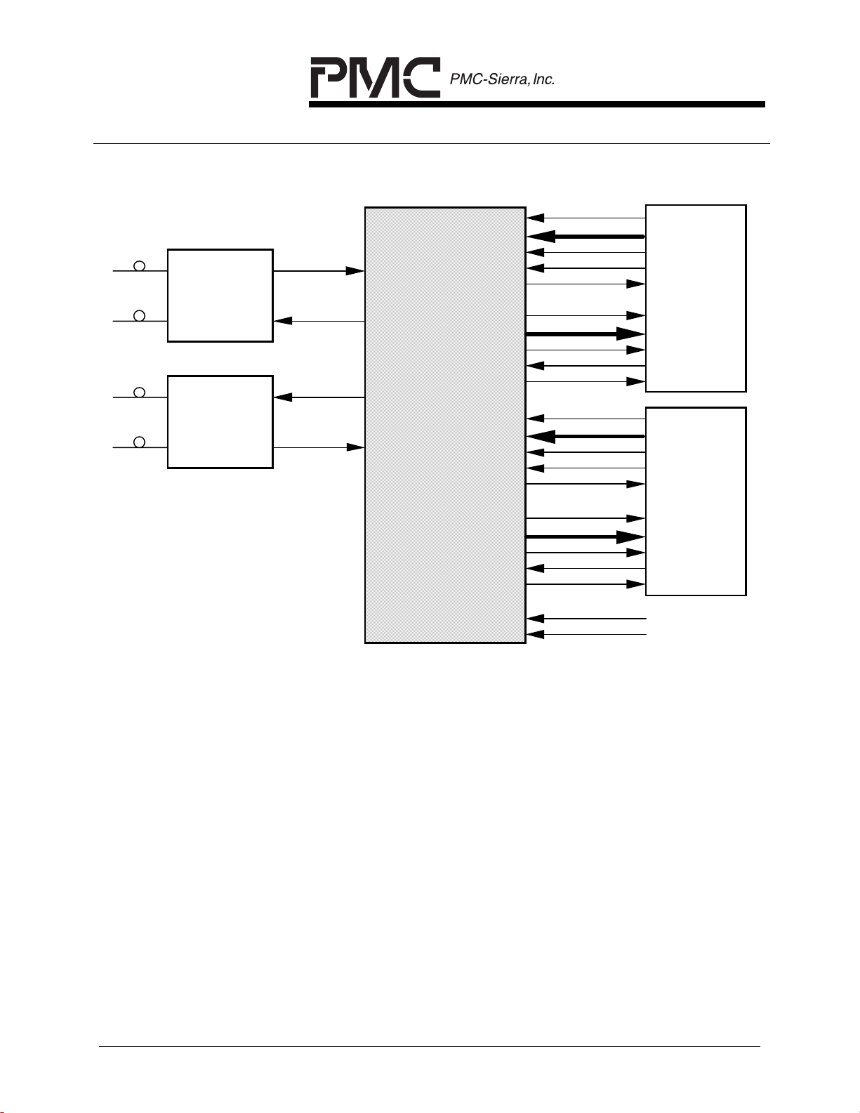
Figure 1 - Split-Bus 8-bit Direct-PHY ATM Switch Interface
TXPRTY[0]
TDAT[7:0]
TSOC1
TWRENB1
TCA1
RXPRTY[0]
RDAT[7:0]
RSOC1
RRDENB1
RCA1
TXPRTY[1]
TDAT[15:8]
TSOC2
TWRENB2
TCA2
ATM
Processor
#1
ATM
Optical
Transceiver
Optical
Transceiver
RXD1+/-
TXD1+/-
TXD2+/-
RXD2+/-
PM5348
S/UNI-DUAL
SATURN
USER NETWORK
INTERFACE
Processor
RXPRTY[1]
RDAT[15:8]
RSOC2
RRDENB2
RCA2
#2
RFCLK
TFCLK
PROPRIETARY AND CONFIDENTIAL TO PMC-SIERRA, INC., AND FOR ITS CUSTOMERS’ INTERNAL USE
7
Page 22
PM5348 S/UNI-DUAL
DATA SHEET
PMC-950919 ISSUE 7 SATURN USER NETWORK INTERFACE
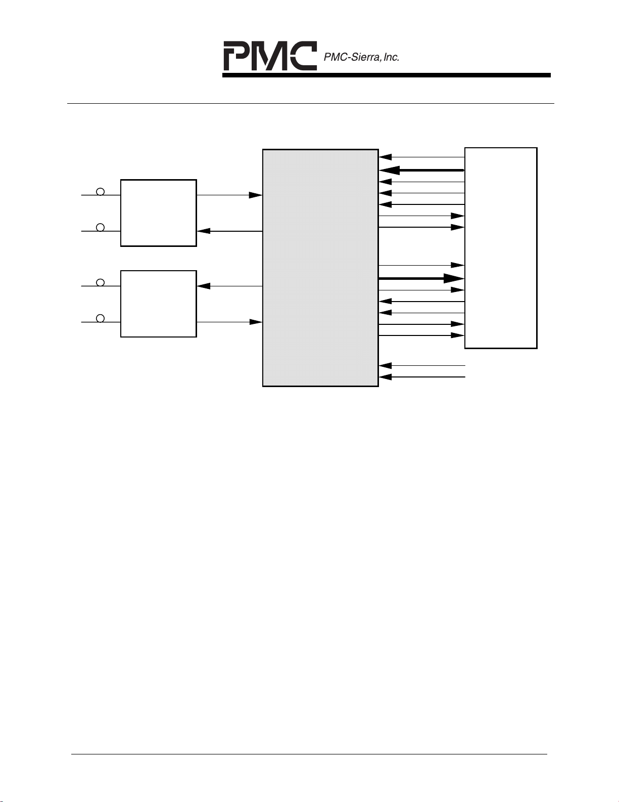
Figure 2 - Direct 8-bit or 16-bit Multi-PHY ATM Switch Interface
TXPRTY[1:0]
TDAT[15:0]
TSOC1
TWRENB1
TWRENB2
TCA1
TCA2
RXPRTY[1:0]
RDAT[15:0]
RSOC1
RRDENB1
RRDENB2
RCA1
RCA2
Multi-
PHY
Controller
Optical
Transceiver
Optical
Transceiver
RXD1+/-
TXD1+/-
TXD2+/-
RXD2+/-
PM5348
S/UNI-DUAL
SATURN
USER NETWORK
INTERFACE
RFCLK
TFCLK
PROPRIETARY AND CONFIDENTIAL TO PMC-SIERRA, INC., AND FOR ITS CUSTOMERS’ INTERNAL USE
8
Page 23
PM5348 S/UNI-DUAL
DATA SHEET
PMC-950919 ISSUE 7 SATURN USER NETWORK INTERFACE
5
RXD1+
RXD1-
ALOS1+
ALOS1-
TXD1+
TXD1-
REFCLK-
TATP
TXD2+
TXD2-
RXD2+
RXD2-
ALOS2+
ALOS2-
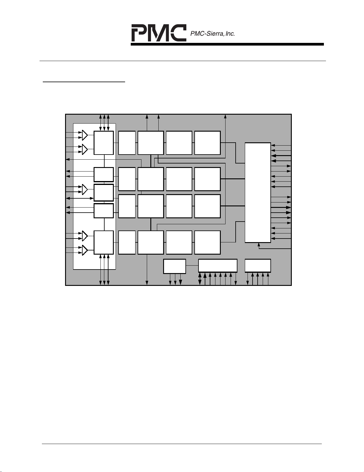
BLOCK DIAGRAM
LF1+
Clock
& Data
Recovery
TFP
Driver
Clk Gen.
Driver
Clock
& Data
Recovery
1
LF1-
LFO1
Serial
Parallel
Framer &
to
Overhead
Process or
RFP
RCLK
Rx
Rx ATM Cell
Process or
Rx ATM
4 Cell
FIFO
TCLK
TSOC2
TSOC1
TXPRTY[1:0]
TDA T[15 :0]
TCA2
P arallel
to
Serial
Para llel
to
Serial
Tx
Fram er &
Over head
Processor
Tx
Fram er &
Over head
Processor
Tx ATM Cell
Process or
Tx ATM Cell
Process or
Tx ATM
4 Cell
FIFO
Tx ATM
4 Cell
FIFO
SCI-PHY
In te rfa ce
TCA1
TWRENB2
TWRENB1
TFCLK REFCLK+
RSOC2
RSOC1
RX PRTY[1:0 ]
RDAT[15:0]
RCA2
RCA1
RRDENB2
RRDENB1
RFCLK
TSEN
Serial
to
Para llel
Rx
Framer &
Overhead
Processor
Rx ATM Cell
Processor
Rx ATM
4 Cell
FIFO
Analog Ed ge
LF2+
Output
Port
2
LF2-
LFO2
RCLK
M1
RAL
M2
RAL
]
:0
[1
T
U
O
Microprocessor I/F
]
]
:0
7
D[
B
B
:0
LE
R
S
8
A
C
RDB
W
A[
JTAG
B
B
O
T
T
D
S
T
IN
R
I
B
S
D
T
M
T
S
TCK
T
R
T
PROPRIETARY AND CONFIDENTIAL TO PMC-SIERRA, INC., AND FOR ITS CUSTOMERS’ INTERNAL USE
9
Page 24

PM5348 S/UNI-DUAL
DATA SHEET
PMC-950919 ISSUE 7 SATURN USER NETWORK INTERFACE
6
DESCRIPTION
The PM5348 Dual SATURN User Network Interface (S/UNI-DUAL) is a
monolithic integrated circuit that implements SONET/SDH processing and ATM
mapping functions for two 155 Mbit/s or 51Mbit/s ATM User Network Interfaces.
It is compliant with SONET and SDH requirements and ATM Forum User
Network Interface specifications. The S/UNI-DUAL is software configurable,
allowing feature selection without changes to external wiring.
The S/UNI-DUAL receives two SONET/SDH channels via separate bit serial
interfaces, recovers their corresponding clock and data, and processes section,
line and path overhead for each channel. Each channel performs framing (A1,
A2), descrambling, detects alarm conditions, and monitors section, line, and path
bit interleaved parity (B1, B2, B3), accumulating error counts at each level for
performance monitoring purposes. Line and path far end block error indications
(M0 or M1, G1) are also accumulated for each channel. Each channel of the
S/UNI-DUAL interprets the received payload pointers (H1, H2) and extracts the
synchronous payload envelope which carries the received ATM cell payload.
Each channel of the S/UNI-DUAL frames to the ATM payload using cell
delineation. HCS error correction is provided. Idle/unassigned cells may be
dropped according to a programmable filter. Cells are also dropped upon
detection of an uncorrectable header check sequence error. The ATM cell
payloads are descrambled. Legitimate ATM cells are written to a four cell FIFO
buffer.
The ATM cells are read from each channel's FIFO via a synchronous interface
with cell-based handshake using either a split 8 bit wide datapath, a direct 8 bit
wide datapath or a direct 16 bit wide datapath. Counts of received ATM cell
headers that are errored and uncorrectable, those that are errored and
correctable, and all passed cells are accumulated independently for each
channel's performance monitoring purposes.
The S/UNI-DUAL transmits two SONET/SDH channels via separate bit serial
interfaces and formats section, line, and path overhead for each channel. Each
channel performs framing pattern insertion (A1, A2), scrambling, alarm signal
insertion, and creates section, line, and path bit interleaved parity (B1, B2, B3)
as required to allow performance monitoring at the far end. Line and path far end
block error indications (M0 or M1, G1) are also inserted.
Each channel of the S/UNI-DUAL generates the payload pointer (H1, H2) and
inserts the synchronous payload envelope which carries the ATM cell payload. It
supports the insertion of a variety of errors into the transmit stream, such as
PROPRIETARY AND CONFIDENTIAL TO PMC-SIERRA, INC., AND FOR ITS CUSTOMERS’ INTERNAL USE
10
Page 25

PM5348 S/UNI-DUAL
DATA SHEET
PMC-950919 ISSUE 7 SATURN USER NETWORK INTERFACE
framing pattern errors, bit interleaved parity errors, and illegal pointers, which are
useful for system diagnostics.
ATM cells are written to each channel's internally programmable-length 4-cell
FIFO via a synchronous interface using either a split 8 bit wide datapath, a direct
8 bit wide datapath, or a direct 16 bit wide datapath. Idle/unassigned cells are
automatically inserted when the internal FIFO contains less than one cell.
Each channel of the S/UNI-DUAL generates the header check sequence and
scrambles the payload of the ATM cells. Payload scrambling can be disabled.
No line rate clocks are required directly by the S/UNI-DUAL as it synthesizes the
transmit clock and recovers the receive clocks using a single 19.44 MHz or 6.48
MHz reference clock.
The S/UNI-DUAL is configured, controlled and monitored via a generic 8-bit
microprocessor bus interface. It is implemented in low power, +5 Volt CMOS
technology. It has TTL and pseudo-ECL (PECL) compatible inputs and
TTL/CMOS compatible outputs and is packaged in a 160 pin MQFP package.
PROPRIETARY AND CONFIDENTIAL TO PMC-SIERRA, INC., AND FOR ITS CUSTOMERS’ INTERNAL USE
11
Page 26
PM5348 S/UNI-DUAL
DATA SHEET
PMC-950919 ISSUE 7 SATURN USER NETWORK INTERFACE
7
PIN DIAGRAM
The S/UNI-DUAL is packaged in a 160 pin MQFP package having a body size of
28mm by 28mm and a pin pitch of 0.65 mm.
C
DC
VS2
]
]
]
D_D
OS1AL
INT B
D[0
R1A
VSS_
VD
D[2
D[1
120
110
100
90
80
R1AVD2
ALOS1+
LF1+
LF1-
LFO 1
R1AVS1
R1AVD1
REFAVS
REFCLKREFCLK+
REFAVD
R1AVSQ 3
RXD1+
RXD1R1AVDQ3
TAVS2
TAVD2
TAVD1
TAVS1
VSS_DC
VDD_DC
TXD1TXD1+
TXVS_AC
R2AVSQ 3
RXD2+
RXD2R2AVDQ3
TXVD_AC
TXD2TXD2+
NC
TATP
R2AVD1
R2AVS1
LFO 2
LF2LF2+
ALOS2+
R2AVD2
PIN 1
TDAT[11]
TDAT[10]
TDAT[9]
TDAT[8]
TDAT[7]
TDAT[6]
TDAT[5]
VDD_DC
TFCLK
VSS_DC
TDAT[4]
TDAT[3]
TDAT[2]
TDAT[1]
TDAT[0]
TSOC2
TSOC1
TCA2
TCA1
VDD_DC
VSS_DC
TW RENB2
TW RENB1
VDD_AC
RFCLK
VSS_AC
RXPRTY[1]
RXPRTY[0]
VDD_DC
VSS_DC
RDAT[15]
RDAT[14]
RDAT[13]
VDD_AC
VSS_AC
RDAT[12]
RDAT[11]
RDAT[10]
RDAT[9]
RDAT[8]
PIN
160
Index
10
20
30
40
12]
TDAT[
13]
TDAT[
14]
TDAT[
15]
TDAT[
TY[0]
TXPR
C
DC
D_D
VSS_
VD
TY[1]
TXPR
C
DC
[0]
[1]
O
LM2
LM1
TD
OUT
TRSTB
TMS
RA
TDI
TCK
RA
150
P
D_D
TSEN
RF
OUT
VSS_
VD
140
LK2
RC
LK1
RC
_AC
K
]
]
]
]
]
D[6
D[4
D[5
D[3
D[7
TFP
VDD
TCL
VSS_AC
130
PM 5348
S/UNI-DUAL
50
60
70
B
C
C
DC
D_D
VSS_
VD
C
[5]
[4]
[3]
[6]
[7]
_AC
RDAT
RDAT
RDAT
VDD
VSS_AC
[2]
[1]
[0]
DC
RDAT
RDAT
VSS_
D_D
VD
_AC
RDAT
RDAT
RDAT
VDD
VSS_AC
OC2
RS
OC1
RS
A2
RC
A1
RC
ENB2
RRD
ENB1
D_D
VD
RRD
DC
RD
VSS_
B
WR
A[2]
A[3]
A[0]
A[4]
A[6]
A[7]
A[8]
ALE
CSB
A[1]
A[5]
VS2
OS2-
RSTB
AL
R2A
PROPRIETARY AND CONFIDENTIAL TO PMC-SIERRA, INC., AND FOR ITS CUSTOMERS’ INTERNAL USE
12
Page 27

PM5348 S/UNI-DUAL
DATA SHEET
PMC-950919 ISSUE 7 SATURN USER NETWORK INTERFACE
8
PIN DESCRIPTION
Pin Name Type Pin
Function
No.
RXD1+
RXD1-
PECL
Input
108
107
The receive differential data inputs (RXD1+,
RXD1-) contain the NRZ bit serial receive
stream for channel #1. The receive clock for
channel #1 is recovered from the RXD1+/bit stream. RXD1+/- must be connected to a
differential data source, single ended
operation is not supported for these inputs.
See note 11.
RXD2+
RXD2-
PECL
Input
95
94
The receive differential data inputs (RXD2+,
RXD2-) contain the NRZ bit serial receive
stream for channel #2. The receive clock for
channel #2 is recovered from the RXD2+/-
bit stream. RXD2+/- must be connected to a
differential data source, single ended
operation is not supported for these inputs.
See note 11.
REFCLK+
REFCLK-
ALOS1+
ALOS1-
PECL
Input
PECL
Input
111
112
119
121
The differential reference clock inputs
(REFCLK+, REFCLK-) contain a jitter-free
19.44 MHz or 6.48 MHz reference clock.
See note 11.
The channel #1 analog loss of signal
(ALOS1+/-) differential inputs are used to
indicate a loss of receive signal power.
When ALOS1+/- is asserted, the data on the
channel #1 receive data (RXD1+/-) pins is
forced to all zeros and the phase locked
loop switches to the reference clock
(REFCLK+/-) to keep the recovered clock in
range. These inputs must be DC coupled.
See note 11.RATP may be bonded to pin
119 or may be accessed accessable during
wafer probe. Channel #1 receive analog test
point (RATP1) is provided for production test
purposes. RATP1 is only available while the
device is in Analog Test Mode.
PROPRIETARY AND CONFIDENTIAL TO PMC-SIERRA, INC., AND FOR ITS CUSTOMERS’ INTERNAL USE
13
Page 28

PM5348 S/UNI-DUAL
DATA SHEET
PMC-950919 ISSUE 7 SATURN USER NETWORK INTERFACE
Pin Name Type Pin
Function
No.
ALOS2+
ALOS2-
PECL
Input
82
80
The channel #2 analog loss of signal
(ALOS2+/-) differential inputs are used to
indicate a loss of receive signal power.
When ALOS2+/- is asserted, the data on the
channel #2 receive data (RXD2+/-) pins is
forced to all zeros and the phase locked
loop switches to the reference clock
(REFCLK+/-) to keep the recovered clock in
range. These inputs must be DC coupled.
See note 11.
RATP may be bonded to pin 82 or may be
accessed accessable during wafer
probe.Channel #2 receive analog test point
(RATP2) is provided for production test
purposes. RATP2 is only available while the
device is in Analog Test Mode.
RCLK1 Output 138 The receive clock (RCLK1) output provides
a timing reference for S/UNI-DUAL channel
#1 receive outputs. RCLK1 is a divide by
eight of the recovered clock. RALM1 is
updated on the rising edge of RCLK1.
RCLK2 Output 139 The receive clock (RCLK2) output provides
a timing reference for S/UNI-DUAL channel
#2 receive outputs. RCLK2 is a divide by
eight of the recovered clock. RALM2 is
updated on the rising edge of RCLK2.
PROPRIETARY AND CONFIDENTIAL TO PMC-SIERRA, INC., AND FOR ITS CUSTOMERS’ INTERNAL USE
14
Page 29

PM5348 S/UNI-DUAL
DATA SHEET
PMC-950919 ISSUE 7 SATURN USER NETWORK INTERFACE
Pin Name Type Pin
Function
No.
RALM1 Output 146 The channel #1 receive alarm (RALM1)
output indicates the state of the receive
framing. RALM1 is low if no receive alarms
are active. RALM1 is high if line AIS, path
AIS, loss of signal (LOS), loss of frame
(LOF), loss of pointer (LOP) or loss of cell
delineation (LCD) is detected in channel #1.
RALM1 is updated on the rising edge of
RCLK1.
RALM1 can be configured to control the
operation of external devices. In this
configuration, the signal levels on RALM1
correspond to register settings.
RALM2 Output 147 The channel #2 receive alarm (RALM2)
output indicates the state of the receive
framing. RALM2 is low if no receive alarms
are active. RALM2 is high if line AIS, path
AIS, loss of signal (LOS), loss of frame
(LOF), loss of pointer (LOP) or loss of cell
delineation (LCD) is detected in channel #2.
RALM2 is updated on the rising edge of
RCLK2.
RALM2 can be configured to control the
operation of external devices. In this
configuration, the signal levels on RALM2
correspond to register settings.
OUT[1]
OUT[0]
Output 145
144
The parallel output port (OUT[1:0]) output is
used to control the operation of external
devices. The signal levels on the parallel
output port correspond to register settings.
PROPRIETARY AND CONFIDENTIAL TO PMC-SIERRA, INC., AND FOR ITS CUSTOMERS’ INTERNAL USE
15
Page 30

PM5348 S/UNI-DUAL
DATA SHEET
PMC-950919 ISSUE 7 SATURN USER NETWORK INTERFACE
Pin Name Type Pin
Function
No.
RFP Output 140 The receive frame pulse (RFP) output is a
selectable 8 kHz signal derived from either
the channel #1 or the channel #2 receive
line clock. RFP pulses high for one
corresponding RCLK cycle every 2430
RCLK cycles for STS-3c (STM-1) TC mode
or every 810 RCLK cycles for STS-1 TC
mode. RFP is updated on the rising edge of
the corresponding RCLK.
TXD1+
TXD1-
TXD2+
TXD2-
Output 98
99
Output 90
91
The transmit differential data outputs
(TXD1+, TXD1-) contain NRZ encoded data
for channel #1.
The transmit differential data outputs
(TXD2+, TXD2-) contain NRZ encoded data
for channel #2.
TFP Output 137 The active high transmit framing pulse (TFP)
output is an 8 kHz timing marker for the
transmitters.
Upon reset the TFP output is held in high
impedance. TFP is enabled as an output
using the TFP_TS bit of register 8.
When enabled, TFP pulses high for one
TCLK cycle every 2430 TCLK cycles for
STS-3c (STM-1) TC mode or every 810
TCLK cycles for STS-1 TC mode. See the
Transmit Section Overhead Processor
section of the Functional Description for
more details on this output.
TFP is updated on the rising edge of TCLK.
PROPRIETARY AND CONFIDENTIAL TO PMC-SIERRA, INC., AND FOR ITS CUSTOMERS’ INTERNAL USE
16
Page 31

PM5348 S/UNI-DUAL
DATA SHEET
PMC-950919 ISSUE 7 SATURN USER NETWORK INTERFACE
Pin Name Type Pin
Function
No.
TSEN Input 143 The tristate enable (TSEN) input selects the
configuration of the receive datapath
(RDAT[15:0], RXPRTY[1:0], RSOC1 and
RSOC2). When TSEN is tied high, the
receive datapath operates as a tristate bus
controlled by RRDENB2 and RRDENB1.
When TSEN is tied low, the receive datapath
is always driven, regardless of the state of
RRDENB2 or RRDENB1. TSEN has an
integral pull up resistor. See note 12.
RFCLK Input 25 The receive read clock (RFCLK) is used to
read ATM cells from the receive FIFOs.
RFCLK must cycle at a 50 MHz or lower
instantaneous rate, but at a high enough
rate to avoid FIFO overflow. RRDENB1 and
RRDENB2 are sampled using the rising
edge of RFCLK. RSOC1, RSOC2,
RDAT[15:0], RXPRTY[1:0], RCA1 and RCA2
are updated on the rising edge of RFCLK.
See note 12.
RRDENB1 Input 62 The channel #1 active low receive read
enable input (RRDENB1) is used to initiate
reads from the channel #1 receive FIFO.
RRDENB1 is sampled using the rising edge
of RFCLK. RRDENB1 must operate in
conjunction with RFCLK to access the FIFO
at a high enough instantaneous rate as to
avoid FIFO overflows. The ATM layer device
may deassert RRDENB1 at anytime it is
unable to accept another byte. See note 12.
PROPRIETARY AND CONFIDENTIAL TO PMC-SIERRA, INC., AND FOR ITS CUSTOMERS’ INTERNAL USE
17
Page 32

PM5348 S/UNI-DUAL
DATA SHEET
PMC-950919 ISSUE 7 SATURN USER NETWORK INTERFACE
Pin Name Type Pin
Function
No.
RRDENB2 Input 61 The channel #2 active low receive read
enable input (RRDENB2) is used to initiate
reads from the channel #2 receive FIFO.
RRDENB2 is sampled using the rising edge
of RFCLK. RRDENB2 must operate in
conjunction with RFCLK to access the FIFO
at a high enough instantaneous rate as to
avoid FIFO overflows. The ATM layer device
may deassert RRDENB2 at anytime it is
unable to accept another byte. See note 12.
RDAT[0]
RDAT[1]
RDAT[2]
RDAT[3]
Tristate
Output
54
53
52
49
The receive cell data (RDAT[15:0]) bus
carries the ATM cell octets that are read
from the receive FIFOs. RDAT[15:0] is
updated on the rising edge of RFCLK and is
tristated when not valid, if the TSEN input is
high. The RDAT[15:0] bus is always driven
RDAT[4]
RDAT[5]
48
47
when TSEN is low, regardless of the level of
RRDENB1 or RRDENB2. See note 12.
RDAT[6]
RDAT[7]
RDAT[8]
RDAT[9]
RDAT[10]
RDAT[11]
RDAT[12]
RDAT[13]
RDAT[14]
RDAT[15]
44
43
40
39
38
37
36
33
32
31
PROPRIETARY AND CONFIDENTIAL TO PMC-SIERRA, INC., AND FOR ITS CUSTOMERS’ INTERNAL USE
18
Page 33

PM5348 S/UNI-DUAL
DATA SHEET
PMC-950919 ISSUE 7 SATURN USER NETWORK INTERFACE
Pin Name Type Pin
No.
RXPRTY[1]
RXPRTY[0]
RSOC1 Tristate
Tristate
Output
27
28
58 The channel #1 receive start of cell
Output
Function
The receive parity (RXPRTY[1:0]) signal
indicates the parity of the RDAT[15:0] bus.
Odd or even parity selection can be made
using a register. RXPRTY[1:0] is updated
on the rising edge of RFCLK and is tristated
when not valid, if the TSEN input is high.
RXPRTY[1:0] is always driven when TSEN
is low, regardless of the level of RRDENB1
or RRDENB2. See note 12.
See the Functional Timing and the RACP
Register Description sections for more
details regarding this output.
(RSOC1) signal marks the start of cell on
the receive cell data bus. When RSOC1 is
high, the first octet of the cell is present on
the receive cell data stream. RSOC1 is
updated on the rising edge of RFCLK and is
tristated when not valid, if the TSEN input is
high. RSOC1 is always driven when TSEN
is low, regardless of the level of RRDENB1
or RRDENB2. See note 12.
RSOC2 Tristate
Output
57 The channel #2 receive start of cell
(RSOC2) signal marks the start of cell on
the channel #2 receive cell data bus (in
Split-Bus mode). When RSOC2 is high, the
first octet of the cell is present on the
receive cell data stream. RSOC2 is updated
on the rising edge of RFCLK and is tristated
when not valid, if the TSEN input is high.
RSOC2 is always driven when TSEN is low,
regardless of the level of RRDENB2. See
note 12.
PROPRIETARY AND CONFIDENTIAL TO PMC-SIERRA, INC., AND FOR ITS CUSTOMERS’ INTERNAL USE
19
Page 34

PM5348 S/UNI-DUAL
DATA SHEET
PMC-950919 ISSUE 7 SATURN USER NETWORK INTERFACE
Pin Name Type Pin
Function
No.
RCA1 Output 60 The channel #1 receive cell available
(RCA1) signal indicates when a cell is
available in the channel #1 receive FIFO.
When RCA1 is sampled asserted, it
indicates that the channel #1 receive FIFO
has at least one cell available to be read.
When RCA1 is sampled deasserted, the
channel #1 receive FIFO contains only four
words or is empty (as selected in the RACP
Configuration register). The active polarity
of RCA1 defaults to active high and can be
programmed in the S/UNI-DUAL
Configuration register. RCA1 is updated on
the rising edge of RFCLK. See note 12.
RCA2 Output 59 The channel #2 receive cell available
(RCA2) signal indicates when a cell is
available in the channel #2 receive FIFO.
When RCA2 is sampled asserted, it
indicates that the channel #2 receive FIFO
has at least one cell available to be read.
When RCA2 is sampled deasserted, the
channel #2 receive FIFO contains only four
words or is empty (as selected in the RACP
Configuration register). The active polarity
of RCA2 defaults to active high and can be
programmed in the S/UNI-DUAL
Configuration register. RCA2 is updated on
the rising edge of RFCLK. See note 12.
PROPRIETARY AND CONFIDENTIAL TO PMC-SIERRA, INC., AND FOR ITS CUSTOMERS’ INTERNAL USE
20
Page 35

PM5348 S/UNI-DUAL
DATA SHEET
PMC-950919 ISSUE 7 SATURN USER NETWORK INTERFACE
Pin Name Type Pin
Function
No.
TCLK Output 136 The transmit byte clock (TCLK) is either a
19.44 MHz or a 6.48 MHz clock derived by
dividing the transmit line rate by eight.
The S/UNI Dual produces two independent
transmit data streams which may have
slightly different data rates depend on the
operation mode. The transmit stream which
TCLK is derived from is dictated by the
configuration of the device. See the Transmit
Section Overhead Processor section of the
Functional Description for more details on
this output.
TFCLK Input 9 The transmit write clock (TFCLK) is used to
write ATM cells to either four cell transmit
FIFOs. TFCLK cycles at a 50 MHz or lower
instantaneous rate. A complete 53 octet cell
must be written to the FIFO before being
inserted in the synchronous payload
envelope (SPE). Idle/unassigned cells are
inserted when a complete cell is not
available. TDAT[15:0], TXPRTY[1:0],
TWRENB1, TWRENB2, TSOC1 and TSOC2
are sampled on the rising edge of TFCLK.
TCA1 and TCA2 are updated on the rising
edge of TFCLK. See note 13.
PROPRIETARY AND CONFIDENTIAL TO PMC-SIERRA, INC., AND FOR ITS CUSTOMERS’ INTERNAL USE
21
Page 36

PM5348 S/UNI-DUAL
DATA SHEET
PMC-950919 ISSUE 7 SATURN USER NETWORK INTERFACE
Pin Name Type Pin
No.
TDAT[0]
TDAT[1]
TDAT[2]
TDAT[3]
TDAT[4]
TDAT[5]
TDAT[6]
TDAT[7]
TDAT[8]
TDAT[9]
TDAT[10]
TDAT[11]
TDAT[12]
Input 15
14
13
12
11
7
6
5
4
3
2
1
160
Function
The transmit cell data (TDAT[15:0]) bus
carries the ATM cell octets. TDAT[15:0] is
sampled on the rising edge of TFCLK and is
considered valid only when TWRENB1 or
TWRENB2 is simultaneously asserted. See
note 13.
TDAT[13]
TDAT[14]
TDAT[15]
TXPRTY[1]
TXPRTY[0]
159
158
157
Input 153
156
The transmit parity (TXPRTY[1:0]) signal
indicates the parity of the TDAT[15:0] bus.
Odd or even parity selection can be made
using a register. TXPRTY[1:0] is sampled
on the rising edge of TFCLK and is
considered valid only when TWRENB1 or
TWRENB2 is simultaneously asserted. See
note 13.
••••••••••••••••••´••••´•j`•••´•••••˙••Ù•••´•••´••••n••
••e interrupt. Cells with parity errors are not
filtered, so the TXPRTY[1:0] inputs may be
unused. See the Functional Timing and the
TACP register description sections for more
details regarding this output.
PROPRIETARY AND CONFIDENTIAL TO PMC-SIERRA, INC., AND FOR ITS CUSTOMERS’ INTERNAL USE
22
Page 37

PM5348 S/UNI-DUAL
DATA SHEET
PMC-950919 ISSUE 7 SATURN USER NETWORK INTERFACE
Pin Name Type Pin
Function
No.
TWRENB1 Input 23 The channel #1 active low transmit write
enable inputs (TWRENB1) is used to initiate
writes to the channel #1 transmit FIFO.
TWRENB1 is sampled using the rising edge
of TFCLK. A complete 53 octet cell must be
written to the transmit FIFO before it is
inserted into the SPE. Idle/unassigned cells
are inserted when a complete cell is not
available. See note 13.
TWRENB2 Input 22 The channel #2 active low transmit write
enable inputs (TWRENB2) is used to initiate
writes to the channel #2 transmit FIFO.
TWRENB2 is sampled using the rising edge
of TFCLK. A complete 53 octet cell must be
written to the transmit FIFO before it is
inserted into the SPE. Idle/unassigned cells
are inserted when a complete cell is not
available. See note 13.
TSOC1 Input 17 The channel #1 transmit start of cell
(TSOC1) signal can be configured to mark a
start of cell on the transmit cell data bus for
channel #1 or channel #2 (in Multi-PHY
mode). When TSOC1 is high, the first octet
of the cell is present. It is not necessary for
TSOC1 to be present at each cell. An
interrupt may be generated if TSOC1 is high
during any byte other than the first byte.
TSOC1 is sampled on the rising edge of
TFCLK. See note 13.
PROPRIETARY AND CONFIDENTIAL TO PMC-SIERRA, INC., AND FOR ITS CUSTOMERS’ INTERNAL USE
23
Page 38

PM5348 S/UNI-DUAL
DATA SHEET
PMC-950919 ISSUE 7 SATURN USER NETWORK INTERFACE
Pin Name Type Pin
Function
No.
TSOC2 Input 16 The channel #2 transmit start of cell
(TSOC2) signal can be configured to mark a
start of cell on the transmit cell data bus for
channel #2 in Split-Bus mode. When
TSOC2 is high, the first octet of the cell is
present. It is not necessary for TSOC2 to be
present at each cell. An interrupt may be
generated if TSOC2 is high during any byte
other than the first byte. TSOC2 is sampled
on the rising edge of TFCLK. See note 13.
TCA1 Output 19 The channel #1 transmit cell available
(TCA1) signal indicates when space for a
cell is available in the channel #1 transmit
FIFO. When TCA1 is sampled asserted, it
indicates that the channel #1 transmit FIFO
is not full. When TCA1 is sampled
deasserted, it indicates that either the
channel #1 transmit FIFO is near full and
can accept no more than four writes, or that
the channel #1 transmit FIFO is full (as
selected in the TACP FIFO Control register).
In addition, to reduce FIFO latency, the
FIFO cell depth can be programmed in the
TACP FIFO Control register. The active
polarity of TCA1 defaults to active high and
can be programmed in the S/UNI-DUAL
Configuration register.
TCA1 is updated on the rising edge of
TFCLK, (see note 13). TCA1 may become
metastable when transitioning from a logic
'1' to '0'.
PROPRIETARY AND CONFIDENTIAL TO PMC-SIERRA, INC., AND FOR ITS CUSTOMERS’ INTERNAL USE
24
Page 39

PM5348 S/UNI-DUAL
DATA SHEET
PMC-950919 ISSUE 7 SATURN USER NETWORK INTERFACE
Pin Name Type Pin
Function
No.
TCA2 Output 18 The channel #2 transmit cell available
(TCA2) signal indicates when space for a
cell is available in the channel #2 transmit
FIFO. When TCA2 is sampled asserted, it
indicates that the channel #2 transmit FIFO
is not full. When TCA2 is sampled
deasserted, it indicates that either the
channel #2 transmit FIFO is near full and
can accept no more than four writes, or that
the channel #2 transmit FIFO is full (as
selected in the TACP FIFO Control register).
In addition, to reduce FIFO latency, the
FIFO cell depth can be programmed in the
TACP FIFO Control register. The active
polarity of TCA2 defaults to active high and
can be programmed in the S/UNI-DUAL
Configuration register.
TCA2 is updated on the rising edge of
TFCLK, (see note 13). TCA2 may become
metastable when transitioning from a logic
'1' to '0'.
TATP Analog 88 Transmit analog test point (TATP) is provided
for production test purposes. Connect this
pin to ground.
LF1+,
LF1-,
LFO1
Analog 118
117
116
Passive components connected to the
channel #1 recovery loop filter (LF1+, LF1-
and LFO1) pins determine the dynamics of
the channel #1 clock recovery unit. Refer to
the Operation section for details.
LF2+,
LF2-,
LFO2
Analog 83
84
85
Passive components connected to the
channel #2 recovery loop filter (LF2+, LF2-
and LFO2) pins determine the dynamics of
the channel #2 clock recovery unit. Refer to
the Operation section for details.
PROPRIETARY AND CONFIDENTIAL TO PMC-SIERRA, INC., AND FOR ITS CUSTOMERS’ INTERNAL USE
25
Page 40

PM5348 S/UNI-DUAL
DATA SHEET
PMC-950919 ISSUE 7 SATURN USER NETWORK INTERFACE
Pin Name Type Pin
Function
No.
CSB Input 67 The active low chip select (CSB) signal is
low during S/UNI-DUAL register accesses.
If CSB is not required (i.e. register accesses
are controlled by using the RDB and WRB
signals only), CSB must be connected to an
inverted version of the RSTB input.
RDB Input 65 The active low read enable (RDB) signal is
low during S/UNI-DUAL register read
accesses. The S/UNI-DUAL drives the
D[7:0] bus with the contents of the
addressed register while RDB and CSB are
low.
WRB Input 66 The active low write strobe (WRB) signal is
low during a S/UNI-DUAL register write
accesses. The D[7:0] bus contents are
clocked into the addressed register on the
rising WRB edge while CSB is low.
D[0]
D[1]
D[2]
D[3]
D[4]
D[5]
D[6]
D[7]
I/O 126
127
128
130
131
132
133
134
The bidirectional data bus D[7:0] is used
during S/UNI-DUAL register read and write
accesses.
PROPRIETARY AND CONFIDENTIAL TO PMC-SIERRA, INC., AND FOR ITS CUSTOMERS’ INTERNAL USE
26
Page 41

PM5348 S/UNI-DUAL
DATA SHEET
PMC-950919 ISSUE 7 SATURN USER NETWORK INTERFACE
Pin Name Type Pin
Function
No.
A[0]
A[1]
A[2]
A[3]
A[4]
A[5]
A[6]
A[7]
Input 77
76
75
74
73
72
71
70
The address bus A[8:0] selects specific
registers during S/UNI-DUAL register
accesses.
A[8]/TRS 69 The test register select (TRS) signal selects
between normal and test mode register
accesses. TRS is high during test mode
register accesses, and is low during normal
mode register accesses.
RSTB Input 78 The active low reset (RSTB) signal provides
an asynchronous S/UNI-DUAL reset. RSTB
is a Schmitt triggered input with an integral
pull up resistor.
ALE Input 68 The address latch enable (ALE) is active
high and latches the address bus A[8:0]
when low. When ALE is high, the internal
address latches are transparent. It allows
the S/UNI-DUAL to interface to a multiplexed
address/data bus. ALE has an integral pull
up resistor.
INTB Open-
Drain
Output
125 The active low interrupt (INTB) signal goes
low when a S/UNI-DUAL interrupt source is
active, and that source is unmasked. The
S/UNI-DUAL may be enabled to report many
alarms or events via interrupts. INTB
returns tristate when the interrupt is
acknowledged via an appropriate register
access.
PROPRIETARY AND CONFIDENTIAL TO PMC-SIERRA, INC., AND FOR ITS CUSTOMERS’ INTERNAL USE
27
Page 42

PM5348 S/UNI-DUAL
DATA SHEET
PMC-950919 ISSUE 7 SATURN USER NETWORK INTERFACE
Pin Name Type Pin
Function
No.
TCK Input 152 The test clock (TCK) signal provides timing
for test operations that can be carried out
using the IEEE P1149.1 test access port.
TMS Input 150 The test mode select (TMS) signal controls
the test operations that can be carried out
using the IEEE P1149.1 test access port.
TMS is sampled on the rising edge of TCK.
TMS has an integral pull up resistor.
TDI Input 151 The test data input (TDI) signal carries test
data into the S/UNI-DUAL via the IEEE
P1149.1 test access port. TDI is sampled
on the rising edge of TCK. TDI has an
integral pull up resistor.
TDO Tristate 148 The test data output (TDO) signal carries
test data out of the S/UNI-DUAL via the
IEEE P1149.1 test access port. TDO is
updated on the falling edge of TCK. TDO is
a tri-state output which is tristate except
when scanning of data is in progress.
TRSTB Input 149 The active low test reset (TRSTB) signal
provides an asynchronous S/UNI-DUAL test
access port reset via the IEEE P1149.1 test
access port. TRSTB is a Schmitt triggered
input with an integral pull up resistor.
TRSTB must be asserted during the power
up sequence.
PROPRIETARY AND CONFIDENTIAL TO PMC-SIERRA, INC., AND FOR ITS CUSTOMERS’ INTERNAL USE
28
Page 43

PM5348 S/UNI-DUAL
DATA SHEET
PMC-950919 ISSUE 7 SATURN USER NETWORK INTERFACE
Pin Name Type Pin
No.
VDD_DC1
VDD_DC2
VDD_DC3
VDD_DC4
VDD_DC5
VDD_DC6
VDD_DC7
VDD_DC8
VDD_DC9
VDD_DC10
VSS_DC1
VSS_DC2
VSS_DC3
Power 8
20
29
42
51
63
100
124
142
154
Ground 10
21
30
Function
The DC power (VDD_DC1 - VDD_DC10)
pins should be connected to a well
decoupled +5 V DC in common with
VDD_AC.
The DC ground (VSS_DC1 - VSS_DC10)
pins should be connected to GND in
common with VSS_AC.
VSS_DC4
VSS_DC5
VSS_DC6
VSS_DC7
VSS_DC8
VSS_DC9
VSS_DC10
VDD_AC1
VDD_AC2
VDD_AC3
VDD_AC4
VDD_AC5
41
50
64
101
123
141
155
Power 24
34
45
55
135
The pad ring power (VDD_AC1 - VDD_AC5)
pins should be connected to a well
decoupled +5 V DC in common with
VDD_DC.
PROPRIETARY AND CONFIDENTIAL TO PMC-SIERRA, INC., AND FOR ITS CUSTOMERS’ INTERNAL USE
29
Page 44

PM5348 S/UNI-DUAL
DATA SHEET
PMC-950919 ISSUE 7 SATURN USER NETWORK INTERFACE
Pin Name Type Pin
Function
No.
VSS_AC1
VSS_AC2
VSS_AC3
VSS_AC4
VSS_AC5
Ground 26
35
46
56
129
The pad ring ground (VSS_AC1 -
VSS_AC5) pins should be connected to
GND in common with VSS_DC.
TAVD1 Power 103 The power (TAVD1) pin for the transmit clock
synthesizer reference circuitry. TAVD1
should be connected to analog +5V.
TAVD2 Power 104 The power (TAVD2) pin for the transmit clock
synthesizer oscillator. TAVD2 should be
connected to analog +5V.
TAVS1 Ground 102 The ground (TAVS1) pin for the transmit
clock synthesizer reference circuitry. TAVS1
should be connected to analog GND.
TAVS2 Ground 105 The ground (TAVS2) pin for the transmit
clock synthesizer oscillator. TAVS2 should
be connected to analog GND.
TXVD_AC Power 92 The transmit pad ring power (TXVD_AC)
supplies the TXD1+/- and TXD2+/- outputs.
TXVD_AC is physically isolated from the
other device power pins and should be a
clean, well decoupled +5 V supply to
minimize the noise coupled into the transmit
stream.
TXVS_AC Ground 97 The transmit pad ring ground (TXVS_AC) is
the return path for the TXD1+/- and TXD2+/-
outputs. TXVS_AC is physically isolated
from the other device ground pins and
should be clean to minimize the noise
coupled into the transmit stream.
R1AVD1 Power 114 The power (R1AVD1) pin for the RXD1+/-
and ALOS1+/- PECL inputs and for channel
#1 receive clock and data recovery block
reference circuitry. R1AVD1 should be
connected to analog +5V.
PROPRIETARY AND CONFIDENTIAL TO PMC-SIERRA, INC., AND FOR ITS CUSTOMERS’ INTERNAL USE
30
Page 45

PM5348 S/UNI-DUAL
DATA SHEET
PMC-950919 ISSUE 7 SATURN USER NETWORK INTERFACE
Pin Name Type Pin
Function
No.
R1AVD2 Power 120 The power (R1AVD2) pin for channel #1
receive clock and data recovery block active
loop filter and oscillator. R1AVD2 should be
connected to analog +5V.
R1AVDQ3 Power 106 R1AVDQ3 acts as a shield and should be
connected to analog +5V.
R1AVS1 Ground 115 The ground (R1AVS1) pin for the RXD1+/-
and ALOS1+/- PECL inputs and for channel
#1 receive clock and data recovery block
reference circuitry. R1AVS1 should be
connected to analog GND.
R1AVS2 Ground 122 The ground (R1AVS2) pin for channel #1
receive clock and data recovery block active
loop filter and oscillator. R1AVS2 should be
connected to analog GND.
R1AVSQ3 Ground 109 R1AVSQ3 acts as a shield and should be
connected to analog GND.
R2AVD1 Power 87 The power (R2AVD1) pin for the RXD2+/-
and ALOS2+/- PECL inputs and for channel
#2 receive clock and data recovery block
reference circuitry. R2AVD1 should be
connected to analog +5V.
R2AVD2 Power 81 The power (R2AVD2) pin for channel #2
receive clock and data recovery block active
loop filter and oscillator. R2AVD2 should be
connected to analog +5V.
R2AVDQ3 Power 93 R2AVDQ3 acts as a shield and should be
connected to analog +5V.
R2AVS1 Ground 86 The ground (R2AVS1) pin for the RXD2+/-
and ALOS2+/- PECL inputs and for channel
#2 receive clock and data recovery block
reference circuitry. R2AVS1 should be
connected to analog GND.
PROPRIETARY AND CONFIDENTIAL TO PMC-SIERRA, INC., AND FOR ITS CUSTOMERS’ INTERNAL USE
31
Page 46

PM5348 S/UNI-DUAL
DATA SHEET
PMC-950919 ISSUE 7 SATURN USER NETWORK INTERFACE
Pin Name Type Pin
Function
No.
R2AVS2 Ground 79 The ground (R2AVS2) pin for channel #2
receive clock and data recovery block active
loop filter and oscillator. R2AVS2 should be
connected to analog GND.
R2AVSQ3 Ground 96 R2AVSQ3 acts as a shield and should be
connected to analog GND.
REFAVD Power 110 The power (REFAVD) pin for the REFCLK+/-
PECL inputs. REFAVD should be connected
to analog +5V.
REFAVS Ground 113 The ground (REFAVS) pin for the
REFCLK+/- PECL inputs. REFAVS should
be connected to analog GND.
NC Ground 89 The no connection (NC) pin should be
connected to analog GND.
Notes on Pin Description:
1. All S/UNI-DUAL inputs and bidirectionals present minimum capacitive loading
and operate at TTL logic levels except for the REFCLK+/-, ALOS1+/-,
ALOS2+/-, RXD1+/- and RXD2+/- differential inputs which operate at pseudo
ECL (PECL) logic levels.
2. The TXD1+/-, and TXD2+/- outputs have a 6 mA drive capability. The
RDAT[15:0], RXPRTY[1:0], RSOC1, RSOC2, RCA1, RCA2, TCA1, TCA2,
TCLK, RCLK1, and RCLK2 outputs have a 4 mA drive capability. All other
S/UNI-DUAL digital outputs and bidirectionals have 2 mA drive capability.
3. Inputs RSTB, ALE, TSEN, TMS, TDI and TRSTB have internal pull-up
resistors.
4. The VSS_DC, VSS_AC, TXVS_AC and AVS ground pins are not internally
connected together. Failure to connect these pins externally may cause
malfunction or damage the S/UNI-DUAL.
5. The VDD_DC, VDD_AC, TXVD_AC, and AVD power pins are not internally
connected together. Failure to connect these pins externally may cause
malfunction or damage the S/UNI-DUAL.
PROPRIETARY AND CONFIDENTIAL TO PMC-SIERRA, INC., AND FOR ITS CUSTOMERS’ INTERNAL USE
32
Page 47

PM5348 S/UNI-DUAL
DATA SHEET
PMC-950919 ISSUE 7 SATURN USER NETWORK INTERFACE
6. All analog power and ground pins are sensitive to noise. They must be
isolated from the digital power and ground. The TAVD2, R1AVD2 and
R2AVD2 pins power oscillators; therefore, they generate significant switching
noise. Care must be taken to decouple these pins from each other and all
other analog power and ground pins.
7. Do not exceed 100 mA of current on any pin during the power-up or powerdown sequence. Refer to the Power Sequencing description in the
Operations section.
8. Before any input activity occurs, ensure that the device power supplies are
within their nominal voltage range.
9. Hold the device in the reset condition until the device power supplies are
within their nominal voltage range.
10. Ensure that all digital power is applied simultaneously, and it is applied before
the analog power is applied. Refer to the Power Sequencing description in
the Operations section.
11. Please refer to the Operation section for a discussion of PECL interfacing
issues.
12. Please refer the Functional Timing Section for a discussion of the Drop Side
Receive Interface.
13. Please refer to the Functional Timing section for a discussion of the Drop
Side Transmit Interface.
PROPRIETARY AND CONFIDENTIAL TO PMC-SIERRA, INC., AND FOR ITS CUSTOMERS’ INTERNAL USE
33
Page 48

PM5348 S/UNI-DUAL
DATA SHEET
PMC-950919 ISSUE 7 SATURN USER NETWORK INTERFACE
9
FUNCTIONAL DESCRIPTION
9.1 Clock Recovery
The clock recovery unit recovers the clock from the incoming bit serial data
stream. The clock recovery unit is fully compliant with SONET and SDH jitter
tolerance requirements. The clock recovery unit utilizes a low frequency
reference clock to train and monitor its clock recovery PLL. Under loss of signal
conditions, the clock recovery unit will continue to output a line rate clock that is
locked to this reference for "keep alive" purposes. The clock recovery unit can
be configured to utilize reference clocks at 6.48 o r 1 9.44 MHz. The clock
recovery unit provides status bits that indicate whether it is locked to the data or
to the reference. The clock recovery unit also supports diagnostic loopback and
a loss of signal input that squelches normal input data.
Initially, the PLL locks to the reference clock, REFCLK+/-. When the frequency of
the recovered clock is within 488 ppm of the reference clock, the PLL attempts
to lock to the data. Once in data lock, the PLL reverts to the reference clock if no
data transitions occur in 80 bit periods or if the recovered clock drifts beyond 488
ppm of the reference clock.
When the transmit clock is derived from the recovered clock (loop timing), the
accuracy of the transmit clock is directly related to the REFCLK+/- reference
accuracy in the case of a loss of signal condition. To meet the GR-253-CORE
SONET Network Element free-run accuracy specification, the reference must be
within +/-20ppm. When not loop timed, the REFCLK+/- accuracy may be relaxed
to +/-50ppm.
The loop filter transfer function is optimized to enable the PLL to track the jitter,
yet tolerate the minimum transition density expected in a received SONET data
signal. The total loop dynamics of the clock recovery PLL yield a jitter tolerance
which exceeds the minimum tolerance required for SONET equipment by GR253-CORE (Figure 3).
PROPRIETARY AND CONFIDENTIAL TO PMC-SIERRA, INC., AND FOR ITS CUSTOMERS’ INTERNAL USE
34
Page 49

PM5348 S/UNI-DUAL
DATA SHEET
PMC-950919 ISSUE 7 SATURN USER NETWORK INTERFACE
Figure 3 - STS-3c/STM-1Jitter Tolerance
100
10
GR-253-CORE
1
Tolerance (Ulpp)
0.1
100 1000 10000 100000 1000000 10000000
Jitter Freq. (Hz)
Note that for frequencies below 300 Hz the jitter tolerance is greater than 15
UIpp; 15 UIpp is the maximum jitter tolerance of the test equipment. Also note
that the dip in the tolerance curve between 300 Hz and 10 kHz is due to the
S/UNI-DUAL's internal clock difference detector. If the recovered clock drifts
beyond 488 ppm of the reference, the PLL locks to the reference clock.
The typical jitter tolerance illustrated in Figure 3 is associated with the external
loop filter components illustrated in Figure 19.
9.2 Serial to Parallel Converter
The Serial to Parallel Converter (SIPO) converts the received bit serial SONET
stream to a byte serial stream. The SIPO searches for the SONET/SDH framing
pattern (A1, A2 ) in the incoming stream, and performs serial to parallel
conversion on octet boundaries.
9.3 Receive Section Overhead Processor
The Receive Section Overhead Processor (RSOP) provides frame
synchronization, descrambling, section level alarm and performance monitoring.
PROPRIETARY AND CONFIDENTIAL TO PMC-SIERRA, INC., AND FOR ITS CUSTOMERS’ INTERNAL USE
35
Page 50

PM5348 S/UNI-DUAL
DATA SHEET
PMC-950919 ISSUE 7 SATURN USER NETWORK INTERFACE
9.3.1 Framer
The Framer Block determines the in-frame/out-of-frame status of the STS-3c or
STS-1 data stream. Output RALM2 or RALM1 can be configured to reflect this
status with its timing aligned to RCLK2 and RCLK1, respectively.
While in-frame, the framing bytes (A1, A2) in each frame are compared against
the expected pattern. Out-of-frame is declared when four consecutive frames
containing one or more framing pattern errors have been received.
While out-of-frame, the SIPO block monitors the bit serial data stream for an
occurrence of the framing pattern. When a framing pattern has been recognized,
the Framer Block verifies that an error free framing pattern is present in the next
frame before declaring in-frame.
9.3.2 Descramble
The Descramble Block utilizes a frame synchronous descrambler to process the
received byte serial stream. The generating polynomial is x7 + x6 + 1 and the
sequence length is 127. Details of the descrambling operation are provided in
the references. Note that the framing bytes (A1 and A2) and the section
trace/section growth bytes (J0/Z0) are not descrambled. A register bit is provided
to disable the descrambling operation.
9.3.3 Error Monitor
The Error Monitor Block calculates the received section BIP-8 error detection
code (B1) based on the scrambled data of the complete STS-3c or STS-1 frame.
The section BIP-8 code is based on a bit interleaved parity calculation using
even parity. Details are provided in the references. The calculated BIP-8 code is
compared with the BIP-8 code extracted from the B1 byte of the following frame.
Differences indicate that a section level bit error has occurred. Up to 64000 (8 x
8000) bit errors can be detected per second. The Error Monitor Block
accumulates these section level bit errors in a 16 bit saturating counter that can
be read via the microprocessor interface. Circuitry is provided to latch this
counter so that its value can be read while simultaneously resetting the internal
counter to 0 or 1, if appropriate, so that a new period of accumulation can begin
without loss of any events. It is intended that this counter be polled at least once
per second so as not to miss bit error events.
PROPRIETARY AND CONFIDENTIAL TO PMC-SIERRA, INC., AND FOR ITS CUSTOMERS’ INTERNAL USE
36
Page 51

PM5348 S/UNI-DUAL
DATA SHEET
PMC-950919 ISSUE 7 SATURN USER NETWORK INTERFACE
9.3.4 Loss of Signal
The Loss of Signal Block monitors the scrambled data of the complete STS-3c or
STS-1 stream for the absence of 1's. When 20 ± 3 µs of all-zeros pattern is
detected, a loss of signal (LOS) is declared. Loss of signal is cleared when two
valid framing words are detected and during the intervening time, no loss of
signal condition is detected. If configured, a loss of signal condition can assert
the corresponding port's RALM output with timing aligned to its respective RCLK.
9.3.5 Loss of Frame
The Loss of Frame Block monitors the in-frame / out-of-frame status of the
Framer Block. A loss of frame (LOF) is declared when an out-of-frame (OOF)
condition persists for 3 ms. To provide for intermittent out-of-frame conditions,
the 3 ms timer is not reset to zero until an in-frame condition persists for 3 ms.
The loss of frame is cleared when an in frame condition persists for a period of 3
ms. If configured, a loss of frame condition can assert the corresponding port's
RALM output with timing aligned to its respective RCLK.
9.4 Receive Line Overhead Processor
The Receive Line Overhead Processor (RLOP) provides line level alarm and
performance monitoring.
9.4.1 Line Remote Defect Indication Detect
The Line RDI Detect Block detects the presence of Line remote defect indication
(RDI) in the data stream. Line RDI is declared when a 110 binary pattern is
detected in bits 6, 7, and 8 of the K2 byte, for five consecutive frames. Line RDI
is removed when any pattern other than 110 is detected in bits 6, 7, and 8 of the
K2 byte for five consecutive frames. The line RDI status is available through a
maskable interrupt and register bits.
9.4.2 Line AIS Detect
The Line AIS Block detects the presence of a Line Alarm Indication Signal (AIS)
in the data stream. Line AIS is declared when a 111 binary pattern is detected in
bits 6,7,8 of the K2 byte, for five consecutive frames. LAIS is removed when any
pattern other than 111 is detected in bits 6, 7, and 8 of the K2 byte for five
consecutive frames. If configured, a line AIS detection can assert the
corresponding port's RALM output with timing aligned to its respective RCLK.
PROPRIETARY AND CONFIDENTIAL TO PMC-SIERRA, INC., AND FOR ITS CUSTOMERS’ INTERNAL USE
37
Page 52

PM5348 S/UNI-DUAL
DATA SHEET
PMC-950919 ISSUE 7 SATURN USER NETWORK INTERFACE
9.4.3 Automatic Protection Switch Control Block
The Automatic Protection Switch Control (APSC) Block filters and captures the
receive automatic protection switch channel bytes (K1 and K2) allowing them to
be read via the RASE APS K1 Register and the RASE APS K2 Register. The
bytes are filtered for three frames before being written to these registers. A
protection switching byte failure alarm is declared when twelve successive
frames have been received, where no three consecutive frames contain identical
K1 bytes. The protection switching byte failure alarm is removed upon detection
of three consecutive frames containing identical K1 bytes. The detection of
invalid APS codes is done in software by polling the RASE APS K1 Register and
the RASE APS K2 Register.
9.4.4 Error Monitor
The Error Monitor Block calculates the received line BIP-8/24 error detection
code (B2) based on the line overhead and synchronous payload envelope of the
receive data stream. The line BIP-8/24 code is a bit interleaved parity calculation
using even parity. Details are provided in the references. The calculated BIP
code is compared with the BIP-8/24 code extracted from the B2 byte(s) of the
following frame. Any differences indicate that a line layer bit error has occurred.
Up to 192000 (24 BIP/frame x 8000 frames/seconde) bit errors can be detected
per second for STS-3 rate and 64000 (8 BIP/frame x 8000 frames/seconde) for
STS-1 rate.
The Error Monitor Block accumulates these line layer bit errors in a 20 bit
saturating counter that can be read via the microprocessor interface. During a
read, the counter value is latched and the counter is reset to 0 (or 1, if there is an
outstanding event). Note, this counter should be polled at least once per second
to avoid saturation which in turn may result in missed bit error events.
Signal fail (SF) or signal degrade (SD) threshold crossing alarms can be
detected and indicated in the Error Monitor Block. The bit error rates associated
with the SF or SD alarms are programmable over a range of 10-3 to 10-9. Details
are provided in the Operations section.
The Error Monitor Block also accumulates line far end block error indications
(contained in the M0/M1 byte) in a similar manner.
PROPRIETARY AND CONFIDENTIAL TO PMC-SIERRA, INC., AND FOR ITS CUSTOMERS’ INTERNAL USE
38
Page 53

PM5348 S/UNI-DUAL
DATA SHEET
PMC-950919 ISSUE 7 SATURN USER NETWORK INTERFACE
9.5 Receive Path Overhead Processor
The Receive Path Overhead Processor (RPOP) provides pointer interpretation,
extraction of path overhead, extraction of the synchronous payload envelope,
and path level alarm and performance monitoring.
9.5.1 Pointer Interpreter
The Pointer Interpreter interprets the incoming pointer (H1, H2) as specified in
the references. The pointer value is used to determine the location of the path
overhead (the J1 byte) in the incoming STS-3c (AU4) or STS-1 (AU3) stream.
The Pointer Interpreter Block detects loss of pointer (LOP) in the incoming STS-1
or STS-3c. LOP is declared as a result of eight consecutive invalid pointers or
eight consecutive NDF enabled indications. LOP is removed when the same
valid pointer with normal NDF is detected for three consecutive frames.
The Pointer Interpreter Block detects path AIS in the incoming STS-1 or STS-3c
stream. PAIS is declared on entry to the AIS_state after three consecutive AIS
indications. PAIS is removed when the same valid pointer with normal NDF is
detected for three consecutive frames or when a valid with NDF enabled is
detected.
The pointer value is used to extract the path overhead from the incoming stream.
Note that due to anomalies in the standard pointer interpretation rules, certain
illegal pointers may not cause the device to declare a loss of pointer (LOP) state.
In this situation, however, the device will declare a loss of cell delineation state
and return to normal operation when presented with legal pointer values. Such
illegal pointers typically can only be generated continuously by test equipment
and will not normally occur during live-traffic operation.
9.5.2 Error Monitor
The Error Monitor Block contains two 16-bit counters that are used to accumulate
path BIP-8 errors (B3), and far end block errors (FEBE). The contents of the two
counters may be transferred to holding registers, and the counters reset under
microprocessor control.
Path BIP-8 errors are detected by comparing the path BIP-8 byte (B3) extracted
from the current frame, to the path BIP-8 computed for the previous frame.
PROPRIETARY AND CONFIDENTIAL TO PMC-SIERRA, INC., AND FOR ITS CUSTOMERS’ INTERNAL USE
39
Page 54

PM5348 S/UNI-DUAL
DATA SHEET
PMC-950919 ISSUE 7 SATURN USER NETWORK INTERFACE
FEBEs are detected by extracting the 4-bit FEBE field from the path status byte
(G1). The legal range for the 4-bit field is between 0000 and 1000, representing
zero to eight errors. Any other value is interpreted as zero errors.
Path remote defect indication (RDI) is detected by extracting bit 5 of the path
status byte. Path RDI is declared when bit 5 is set high for five consecutive
frames and is cleared when bit 5 is low for five consecutive frames.
9.6 Receive ATM Cell Processor
The Receive ATM Cell Processor (RACP) performs ATM cell delineation,
provides cell filtering based on idle/unassigned cell detection and HCS error
detection, and performs ATM cell payload descrambling. The RACP also
provides a four cell deep receive FIFO. This FIFO passes a 53 byte data
structure and is used to separate the line timing from the higher layer ATM
system timing.
9.6.1 Cell Delineation
Cell Delineation is the process of framing to ATM cell boundaries using the
header check sequence (HCS) field found in the cell header. The HCS is a
CRC-8 calculation over the first 4 octets of the ATM cell header. When
performing delineation, correct HCS calculations are assumed to indicate cell
boundaries. Cells must be byte aligned before insertion in the synchronous
payload envelope.
The cell delineation algorithm searches the 53 possible cell boundary candidates
one at a time to determine the valid cell boundary location. While searching for
the cell boundary location, the cell delineation circuit is in the HUNT state. When
a correct HCS is found, the cell delineation state machine locks on the particular
cell boundary and enters the PRESYNC state. This state validates the cell
boundary location. If the cell boundary is invalid then an incorrect HCS will be
received within the next DELTA cells, at which point a transition back to the
HUNT state is executed. If no HCS errors are detected in this PRESYNC period
then the SYNC state is entered. While in the SYNC state, synchronization is
maintained until ALPHA consecutive incorrect HCS patterns are detected. In
such an event a transition is made back to the HUNT state. The state diagram of
the delineation process is shown in Figure 4.
PROPRIETARY AND CONFIDENTIAL TO PMC-SIERRA, INC., AND FOR ITS CUSTOMERS’ INTERNAL USE
40
Page 55

PM5348 S/UNI-DUAL
DATA SHEET
PMC-950919 ISSUE 7 SATURN USER NETWORK INTERFACE
Figure 4 - Cell Delineation State Diagram
correct HCS
(byte by byte)
HUNT
Incorrect HCS
(cell by cell)
ALPHA
consecutive
incorrect HCS's
(cell by cell)
SYNC
PRESYNC
DELTA
consecutive
correct HCS's
(cell by cell)
The values of ALPHA and DELTA determine the robustness of the delineation
method. ALPHA determines the robustness against false misalignments due to
bit errors. DELTA determines the robustness against false delineation in the
synchronization process. ALPHA is chosen to be 7 and DELTA is chosen to be
6. These values result in a maximum average time to delineate of 31 µs for STS3c and 93 µs for STS-1.
9.6.2 Descrambler
The self synchronous descrambler operates on the 48 byte cell payload only.
The circuitry descrambles the information field using the 'x43 + 1' polynomial.
The descrambler is disabled for the duration of the header and HCS fields, and
may optionally be disabled.
9.6.3 Cell Filter and HCS Verification
Cells are filtered (or dropped) based on HCS errors and/or a cell header pattern.
Cell filtering is optional and is enabled through the RACP registers. Cells are
passed to the receive FIFO while the cell delineation state machine is in the
SYNC state as described above. When both filtering and HCS checking are
PROPRIETARY AND CONFIDENTIAL TO PMC-SIERRA, INC., AND FOR ITS CUSTOMERS’ INTERNAL USE
41
Page 56

PM5348 S/UNI-DUAL
DATA SHEET
PMC-950919 ISSUE 7 SATURN USER NETWORK INTERFACE
enabled, cells are dropped if uncorrectable HCS errors are detected, or if the
corrected header contents match the pattern contained in the 'Match Header
Pattern' and 'Match Header Mask' registers. Idle or unassigned cell filtering is
accomplished by writing the appropriate cell header pattern into the 'Match
Header Pattern' and 'Match Header Mask' registers. Idle/Unassigned cells are
assumed to contain the all zeros pattern in the VCI and VPI fields. The 'Match
Header Pattern' and 'Match Header Mask' registers allow filtering control over the
contents of the GFC, PTI, and CLP fields of the header.
The HCS is a CRC-8 calculation over the first 4 octets of the ATM cell header.
The RACP block verifies the received HCS using the polynomial, x8 + x2 + x + 1.
The coset polynomial, x6 + x4 + x2 + 1, is added (modulo 2) to the received HCS
octet before comparison with the calculated result. While the cell delineation
state machine (described above) is in the SYNC state, the HCS verification
circuit implements the state machine shown in Figure 5.
Figure 5 - HCS Verification State Diagram
No Errors
Detected
(Pass Cell)
DELTA
consecutive
correct HCS's
(From PRESYNC
state)
ATM DELINEATION
SYNC
CORRECTION
MODE
STATE
Apparant Multi-Bit Error
Single Bit Error
(Correct Error
and Pass Cell)
No Errors Detected
(Pass Cell)
ALPHA
consecutive
incorrect HCS's
(To HUNT state)
(Drop Cell)
Errors
Detected
(Drop Cell)
DETECTION
MODE
PROPRIETARY AND CONFIDENTIAL TO PMC-SIERRA, INC., AND FOR ITS CUSTOMERS’ INTERNAL USE
42
Page 57

PM5348 S/UNI-DUAL
DATA SHEET
PMC-950919 ISSUE 7 SATURN USER NETWORK INTERFACE
In normal operation, the HCS verification state machine remains in the
'Correction Mode' state. Incoming cells containing no HCS errors are passed to
the receive FIFO. Incoming single bit errors are corrected, and the resulting cell
is passed to the FIFO. Upon detection of a single bit error or a multi bit error, the
state machine transitions to the 'Detection Mode' state. In this state, the
detection of any HCS error causes the corresponding cell to be dropped. Cells
containing an error-free HCS are passed, and the state machine transitions back
to the 'Correction Mode' state.
9.6.4 Performance Monitor
The Performance Monitor consists of two 8-bit saturating HCS error event
counters and a 19-bit cell counter. One of the counters accumulates correctable
HCS errors (i.e. single HCS bit errors detected while the HCS Verification state
machine is in the 'Correction Mode' state described above). The second counter
accumulates uncorrectable HCS errors (i.e. HCS bit errors detected while the
HCS Verification state machine is in the 'Detection Mode' state or multiple HCS
bit errors detected while the state machine is in the 'Correction Mode' state as
described above). The cell counter accumulates the number of received
assigned cells. All counters are enabled only when the RACP is in the SYNC
state.
Each counter may be read through the microprocessor interface. Circuitry is
provided to latch these counters so that their values can be read while
simultaneously resetting the internal counters to 0 or 1, if appropriate, so that a
new period of accumulation can begin without loss of any events. It is intended
that the counters be polled at least once per second so HCS error events or cell
counts will not be missed.
9.6.5 Receive FIFO
The Receive FIFO provides FIFO management and the asynchronous interface
between the RACP block and chip pads to the external environment. The receive
FIFO can accommodate four cells. The receive FIFO provides for the separation
of the STS-1 or STS-3c line or physical layer timing from the ATM laye r timing.
Management functions include filling the receive FIFO, indicating when cells are
available to be read from the receive FIFO, maintaining the receive FIFO read
and write pointers, and detecting FIFO overrun and underrun conditions. Upon
detection of an overrun condition, the FIFO will drop all incoming cells until at
least one cell has been read from the FIFO. At least one cell will be lost during
PROPRIETARY AND CONFIDENTIAL TO PMC-SIERRA, INC., AND FOR ITS CUSTOMERS’ INTERNAL USE
43
Page 58

PM5348 S/UNI-DUAL
DATA SHEET
PMC-950919 ISSUE 7 SATURN USER NETWORK INTERFACE
the FIFO drop operation. Upon detection of an underrun, the offending read is
ignored. FIFO overruns are indicated through a maskable interrupt and register
bit. The interface provided indicates the start of a cell (RSOC) when data is read
from the receive FIFO (using RFCLK) and indicates the cell available status
(RCA). The cell available status may be configured to change from available to
unavailable on read cell boundaries or four reads before the cell boundary.
When the RCA signal is configured to be deasserted with zero octets (as
opposed to four) in the FIFO, it is not an error condition to hold the read enable
(RRDENB) active. In this situation, the RCA signal identifies the valid octets.
9.7 Clock Synthesis
The transmit clock is synthesized from a 19.44 MHz or 6.48 MHz reference. The
transfer function yields a typical low pass corner of 500 kHz with a 19.44 MHz
reference and 170 kHz with a 6.48 MHz reference, above which reference jitter is
attenuated at 12dB per octave. The intrinsic jitter is minimised when the
reference frequency is 19.44 MHz. With a jitter free 19.44 MHz differential
reference input and a low noise board layout, the intrinsic jitter is typically 0.01 UI
RMS when measured using a high pass filter with a 12 kHz cutoff frequency.
The REFCLK+/- reference should be within ±20 ppm to meet the SONET freerun accuracy requirements specified in GR-253-CORE.
9.8 Parallel to Serial Converter
The Parallel to Serial Converter (PISO) converts the internal byte serial stream to
a bit serial stream.
9.9 Transmit Section Overhead Processor
The Transmit Section Overhead Processor (TSOP) provides frame pattern
insertion (A1, A2), scrambling, section level alarm signal insertion, and section
BIP-8 (B1) insertion.
9.9.1 Line AIS Insert
Line AIS insertion results in all bits of the SONET/SDH frame being set to 1
before scrambling except for the section overhead. The Line AIS Insert Block
substitutes all ones as described when enabled through an internal register
accessed through the microprocessor interface. Activation or deactivation of line
AIS insertion is synchronized to frame boundaries.
PROPRIETARY AND CONFIDENTIAL TO PMC-SIERRA, INC., AND FOR ITS CUSTOMERS’ INTERNAL USE
44
Page 59

PM5348 S/UNI-DUAL
DATA SHEET
PMC-950919 ISSUE 7 SATURN USER NETWORK INTERFACE
9.9.2 BIP-8 Insert
The BIP-8 Insert Block calculates and inserts the BIP-8 error detection code (B1)
into the unscrambled data stream.
The BIP-8 calculation is based on the scrambled data of the complete STS-3c or
STS-1 frame. The section BIP-8 code is based on a bit interleaved parity
calculation using even parity. Details are provided in the references. The
calculated BIP-8 code is then inserted into the B1 byte of the following frame
before scrambling. BIP-8 errors may be continuously inserted under register
control for diagnostic purposes.
9.9.3 Framing and Section Trace
The Framing and Section Trace Block inserts the framing bytes (A1, A2) and
section trace/section growth bytes (J0/Z0) into the STS-3c or STS-1 frame.
Framing bit errors may be continuously inserted under register control for
diagnostic purposes.
9.9.4 Generation of TFP
The TSOP generates a Transmit Framing Pulse (TFP) which is high for one TCLK
cycle every 2430 TCLK cycles for STS-3c TC mode (STS-1 mode) or every 810
cycles for STS-1 TC mode.
Each channel of the S/UNI Dual contains a TSOP block and each of the
channels may have independent transmit line rates depending on the source of
the transmit clock. The source of the transmit clock may be obtained from the
REFCLK+/- inputs or it may be derived from the received data (loop timed or line
looped back modes). As a result, the two halves of the S/UNI Dual may generate
different TFPs derived from different transmit clocks.
The S/UNI Dual selects the TCLK and TFP outputs depending whether the
device is loop timed or in line loop back mode according to the following table:
PROPRIETARY AND CONFIDENTIAL TO PMC-SIERRA, INC., AND FOR ITS CUSTOMERS’ INTERNAL USE
45
Page 60

PM5348 S/UNI-DUAL
DATA SHEET
PMC-950919 ISSUE 7 SATURN USER NETWORK INTERFACE
Table 1 -
CH #1 Loop
timed or Line
Looped back
NO NO Channel 1 Channel 1
NO YES Channel 1 Channel 1
YES NO Channel 2 Channel 2
YES YES Forced Low Force Low
To summarize the table above, TFP and TCLK are taken from the channel which
is not looped timed or in line loop back mode. In the case where neither is, then
TFP and TCLK are taken from channel 1. In the case were both are, TFP and
TCLK are forced low.
Looped timed mode or line loop back mode is selected using registers 0x05 and
0x085.
9.9.5 Scrambler
The Scrambler Block utilizes a frame synchronous scrambler to process the
transmit serial stream when enabled through an internal register accessed via
the microprocessor interface. The generating polynomial is x7 + x6 + 1. Precise
details of the scrambling operation are provided in the references. Note that the
framing bytes and the identity bytes are not scrambled. All zeros may be
continuously inserted (after scrambling) under register control for diagnostic
purposes.
CH #2 Loop
timed or Line
Looped back
TFP Output
Source
TCLK Output
Source
9.10 Transmit Line Overhead Processor
The Transmit Line Overhead Processor (TLOP) provides line level alarm signal
insertion, synchronization status insertion (S1), and line BIP-8/24 insertion (B2).
9.10.1 APS Insert
The APS Insert Block inserts the two automatic protection switch (APS) channel
bytes in the Line Overhead (K1 and K2) into the transmit stream when enabled
by an internal register.
PROPRIETARY AND CONFIDENTIAL TO PMC-SIERRA, INC., AND FOR ITS CUSTOMERS’ INTERNAL USE
46
Page 61

PM5348 S/UNI-DUAL
DATA SHEET
PMC-950919 ISSUE 7 SATURN USER NETWORK INTERFACE
9.10.2 BIP Calculate
The BIP Calculate Block calculates the line BIP error detection code (B2) based
on the line overhead and synchronous payload envelope of the STS-3c or STS-1
stream. The line BIP code is a bit interleaved parity calculation using even parity.
Details are provided in the references. The calculated BIP code is inserted into
the B2 byte positions of the following frame. BIP errors may be continuously
inserted under register control for diagnostic purposes.
9.10.3 Line Remote Defect Indication Insert
The Line RDI Insert Block multiplexes the line overhead bytes into the output
stream and optionally inserts line RDI. Line RDI is inserted by this block when
enabled via register control. Line RDI is inserted by transmitting the code 110
(binary) in bit positions 6, 7, and 8 of the K2 byte contained in the STS-3c or
STS-1 stream.
9.10.4 Line FEBE Insert
The Line FEBE Insert Block accumulates line BIP errors (M0/M1) detected by
the Receive Line Overhead Processor and encodes far end block error
indications in the transmit M0/M1 byte.
PROPRIETARY AND CONFIDENTIAL TO PMC-SIERRA, INC., AND FOR ITS CUSTOMERS’ INTERNAL USE
47
Page 62

PM5348 S/UNI-DUAL
DATA SHEET
PMC-950919 ISSUE 7 SATURN USER NETWORK INTERFACE
Figure 6 - STS-3c/STM-1 Default Transport Overhead Values
A1
(0xF6)
B1
(*)
A1
(0xF6)
(0x00) (0x00)
A1
(0xF6)
D1
(0x00) (0x00) (0x00)
H1
(0x62)
B2
(*)
H1
(0x93)
B2
(*)
H1
(0x93)
B2
(*)
D4
(0x00) (0x00) (0x00)
D7
(0x00) (0x00) (0x00)
D10
(0x00) (0x00) (0x00)
S1
(0x00)
Z1
(0x00)
Z1
(0x00)
A2
(0x28)
A2
(0x28)
A2
(0x28)
E1
(0x00) (0x00) (0x00)
D2
(0x00) (0x00) (0x00)
H2
(0x0A)
H2
(0xFF)
H2
(0xFF)
K1
(0x00) (0x00) (0x00)
D5
(0x00) (0x00) (0x00)
D8
(0x00) (0x00) (0x00)
D11
(0x00) (0x00) (0x00)
Z2
(0x00)
Z2
(0x00)
M1
(*)
J0
(0x01)
Z0
(0x02)
Z0
(0x03)
F1
(0x00) (0x00) (0x00)
D3
(0x00) (0x00) (0x00)
H3
(0x00)
H3
(0x00)
H3
(0x00)
K2
(0x00) (0x00) (0x00)
D6
(0x00) (0x00) (0x00)
D9
(0x00) (0x00) (0x00)
D12
(0x00) (0x00) (0x00)
E2
(0x00) (0x00) (0x00)
* : B1, B2 values depend on payload contents
M1 value depends on incoming line bit errors
PROPRIETARY AND CONFIDENTIAL TO PMC-SIERRA, INC., AND FOR ITS CUSTOMERS’ INTERNAL USE
48
Page 63

PM5348 S/UNI-DUAL
DATA SHEET
PMC-950919 ISSUE 7 SATURN USER NETWORK INTERFACE
Figure 7 - STS-1 Default Transport Overhead Values
A1
(0xF6)
B1
(*)
D1
(0x00)
H1
(0x62)
B2
(*)
D4
(0x00)
D7
(0x00)
D10
(0x00)
S1
(0x00)
A2
(0x28)
E1
(0x00)
D2
(0x00)
H2
(0x0A)
K1
(0x00)
D5
(0x00)
D8
(0x00)
D11
(0x00)
M0
(*)
J0
(0x01)
F1
(0x00)
D3
(0x00)
H3
(0x00)
K2
(0x00)
D6
(0x00)
D9
(0x00)
D12
(0x00)
E2
(0x00)
* : B1, B2 values depend on payload contents
M0 value depends on incoming line bit errors
9.11 Transmit Path Overhead Processor
The Transmit Path Overhead Processor (TPOP) provides transport frame
alignment generation, pointer generation (H1, H2), path overhead insertion,
insertion of the synchronous payload envelope, insertion of path level alarm
signals and path BIP-8 (B3) insertion.
9.11.1 Pointer Generator
The Pointer Generator Block generates the outgoing payload pointer (H1, H2).
The block contains a free running timeslot counter that locates the start of the
PROPRIETARY AND CONFIDENTIAL TO PMC-SIERRA, INC., AND FOR ITS CUSTOMERS’ INTERNAL USE
49
Page 64

PM5348 S/UNI-DUAL
DATA SHEET
PMC-950919 ISSUE 7 SATURN USER NETWORK INTERFACE
synchronous payload envelope based on the generated pointer value and the
SONET/SDH frame alignment.
The Pointer Generator Block generates the outgoing pointer as specified in the
references. The concatenation indication (the NDF field set to 1001, I-bits and
D-bits set to all ones, and unused bits set to all zeros) is inserted in the second
and third pointer bytes.
9.11.2 BIP-8 Calculate
The BIP-8 Calculate Block performs a path bit interleaved parity calculation on
the SPE of the outgoing stream. The resulting parity byte is inserted in the path
BIP-8 (B3) byte position of the subsequent frame. BIP-8 errors may be
continuously inserted under register control for diagnostic purposes.
9.11.3 FEBE Calculate
The FEBE Calculate Block accumulates far end block errors on a per frame
basis, and inserts the accumulated value (up to maximum value of eight) in the
FEBE bit positions of the path status (G1) byte. The FEBE information is derived
from path BIP-8 errors detected by the receive path overhead processor, RPOP.
The asynchronous nature of these signals implies that more than eight FEBE
events may be accumulated between transmit G1 bytes. If more than eight
receive Path BIP-8 errors are accumulated between transmit G1 bytes, the
accumulation counter is decremented by eight, and the remaining FEBEs are
transmitted at the next opportunity. Far end block errors may be inserted under
register control for diagnostic purposes.
9.11.4 SPE Multiplexer
The SPE Multiplexer Block multiplexes the payload pointer bytes, the SPE
stream, and the path overhead bytes into the STS-3c or STS-1 stream.
PROPRIETARY AND CONFIDENTIAL TO PMC-SIERRA, INC., AND FOR ITS CUSTOMERS’ INTERNAL USE
50
Page 65

PM5348 S/UNI-DUAL
DATA SHEET
PMC-950919 ISSUE 7 SATURN USER NETWORK INTERFACE
Figure 8 - Default Path Overhead Values
J1
(0x00)
B3
(*)
C2
(0x13)
G1
(*)
F2
(0x00)
H4
(*)
* : B3 value depend on payload contents
G1 value depends on incoming path bit errors
H4 value depends on cell boundary offset
9.12 Transmit ATM Cell Processor
The Transmit ATM Cell Processor (TACP) inserts H4 framing, provides rate
adaptation via idle/unassigned cell insertion, provides HCS generation and
insertion, and performs ATM cell scrambling. The TACP contains a four cell
transmit FIFO. An idle or unassigned cell is transmitted if a complete ATM cell
has not been written into the FIFO.
Z3
(0x00)
Z4
(0x00)
Z5
(0x00)
PROPRIETARY AND CONFIDENTIAL TO PMC-SIERRA, INC., AND FOR ITS CUSTOMERS’ INTERNAL USE
51
Page 66

PM5348 S/UNI-DUAL
DATA SHEET
PMC-950919 ISSUE 7 SATURN USER NETWORK INTERFACE
9.12.1 Idle/Unassigned Cell Generator
The Idle/Unassigned Cell Generator inserts idle or unassigned cells into the cell
stream when enabled. Registers are provided to program the GFC, PTI, and
CLP fields of the idle cell header and the idle cell payload. An all zeros pattern is
insert ed into the VCI/VPI bit locations. The idle cell HCS is automatically
calculated and inserted.
9.12.2 Scrambler
The Scrambler scrambles the 48 octet information field. Scrambling is performed
using a parallel implementation of the self synchronous scrambler described in
the references. The cell headers are transmitted unscrambled, and the
scrambler may optionally be completely disabled.
9.12.3 HCS Generator
The HCS Generator performs a CRC-8 calculation over the first four header
octets. A parallel implementation of the polynomial, x8+x2+x+1, is used. The
coset polynomial, x6+x4+x2+1, is added (modulo 2) to the residue. The HCS
Generator inserts the result into the fifth octet of the header.
9.12.4 Transmit FIFO
The Transmit FIFO provides FIFO management and a synchronous interface
between the S/UNI-DUAL device and the external environment. The transmit
FIFO can accommodate four cells. It provides for the separation of the physical
layer timing from the ATM layer timing.
Management functions include filling the transmit FIFO, indicating when cells are
available to be written to the transmit FIFO, maintaining the transmit FIFO read
and write pointers, and detecting a FIFO overrun condition. The synchronous
interface provided to an external device expects the start of a cell (TSOC) when
the first byte of the cell is written to the FIFO (using TFCLK in conjunction with
TWRENB) and indicates the cell available status (TCA). The FIFO status
changes from cell unavailable to cell available on read cell boundaries. The FIFO
status can be configured to change from cell available to cell unavailable on write
cell boundaries or four octets before the end of the cell.
The latency through the transmit FIFO can be controlled by setting the fill level at
which the cell available (TCA) signal is deasserted. Although all four cell buffers
PROPRIETARY AND CONFIDENTIAL TO PMC-SIERRA, INC., AND FOR ITS CUSTOMERS’ INTERNAL USE
52
Page 67

PM5348 S/UNI-DUAL
DATA SHEET
PMC-950919 ISSUE 7 SATURN USER NETWORK INTERFACE
are always accessible, TCA may be programmed to indicate when the FIFO
contains one, two, three or four cells. (The current cell being read out of the
FIFO is included in the count. Be aware that setting a depth of one may limit
throughput.) If a cell write is started immediately after TCA transitions from
deasserted to asserted, the latency through the device for the cell being written
in STS-3c/STM-1 is:
latency = depth*(53 line byte periods) + 16 line byte periods
(min.)
= depth*(53 line byte periods) + 26 line byte periods
(max.).
The latency for the cell being written in STS-1 is:
latency = depth*(53 line byte periods) + 10 line byte periods
(min.)
= depth*(53 line byte periods) + 14 line byte periods
(max.).
The presence of the SONET/SDH overhead accounts for the difference between
the minimum and maximum latencies.
When the FIFO contains four cells and the upstream device writes into the FIFO,
the TACP indicates a FIFO overrun condition using a maskable interrupt and
register bits. The offending write and all subsequent writes are ignored until
there is room in the FIFO.
9.13 Saturn Compliant Split-Bus PHY Interface (SPHY)
The Saturn Compliant Split-Bus PHY Interface block (SPHY) permits the two
receive cell FIFOs (RXFF) and the two transmit cell FIFOs (TXFF) to share a
single cell interface on the S/UNI-DUAL.
Two interface modes are supported: 1) Split-Bus Direct-PHY addressing (when
the SPLIT bit in S/UNI-DUAL Interface Control register is logic 1), and 2) MultiPHY selection (when the SPLIT bit is logic 0).
When Split-Bus addressing is enabled, both transmit/receive FIFOs are
accessible. The FIFOs are limited to 8-bit mode. The transmit FIFO for channel
#1 uses TD AT[7:0], TSOC[1], TWRENB[1], TCA[1] and TXPR TY[0]. The transmit
FIFO for channel #2 uses TDAT[15:8], TSOC[2], TWRENB[2], TCA[2] and
TXPRTY[1]. The receive FIFO for channel #1 uses RDAT[7:0], RSOC[1],
RRDENB[1], RCA[1] and RXPRTY[0]. The receive FIFO for channel #2 uses
RDAT[15:8], RSOC[2], RRDENB[2], RCA[2] and RXPRTY[1].
PROPRIETARY AND CONFIDENTIAL TO PMC-SIERRA, INC., AND FOR ITS CUSTOMERS’ INTERNAL USE
53
Page 68

PM5348 S/UNI-DUAL
DATA SHEET
PMC-950919 ISSUE 7 SATURN USER NETWORK INTERFACE
When Multi-PHY selection is enabled, one of two possible transmit/receive FIFOs
is selected by the corresponding TWRENB[2:1]/RRDENB[2:1] signal respectively.
The cell available status fo r each of the transmit and receive FIFOs is directly
available on RCA[2:1] and TCA[2:1]. The transmit/receive FIFOs can operate in
8-bit mode (BUS8 bit in S/UNI-DUAL is logic 1) or in 16-bit mode (BUS8 bit is
logic 0). With Multi-PHY selected, TSOC[2] and RSOC[2] are not used.
9.14 Microprocessor Interface
The microprocessor interface block provides normal and test mode registers, and
the logic required to connect to the microprocessor interface. The normal mode
registers are required for normal operation, and test mode registers are used to
enhance the testability of the S/UNI-DUAL.
PROPRIETARY AND CONFIDENTIAL TO PMC-SIERRA, INC., AND FOR ITS CUSTOMERS’ INTERNAL USE
54
Page 69

PM5348 S/UNI-DUAL
DATA SHEET
PMC-950919 ISSUE 7 SATURN USER NETWORK INTERFACE
10
REGISTER MEMORY MAP
Address Register
#1 #2
0x000 S/UNI-DUAL Master Reset and Identity / Channel #1
0x080 S/UNI-DUAL Channel #2 Monitoring Update
0x001 0x081 S/UNI-DUAL Configuration
0x002 0x082 S/UNI-DUAL Interrupt Status
0x003 S/UNI-DUAL Master Mode Control
0x083 Reserved
0x004 S/UNI-DUAL Master Clock Monitor
0x084 Reserved
0x005 0x085 S/UNI-DUAL Control
0x006 S/UNI-DUAL Clock Synthesis Control and Status
Monitoring Update
0x086 Reserved
0x007 0x087 S/UNI-DUAL Clock Recovery Control and Status
0x008 S/UNI-DUAL Interface Control
0x009 S/UNI-DUAL Output Port Control
0x00A S/UNI-DUAL POP[0] Strobe Rate
0x00B S/UNI-DUAL POP[1] Strobe Rate
0x00C S/UNI-DUAL POP[2] Strobe Rate
0x00D S/UNI-DUAL POP[3] Strobe Rate
0x088-0x08D Reserved
0x00E 0x08E Transmit Synchronization Status
0x00F 0x08F Reserved
0x010 0x090 RSOP Control/Interrupt Enable
0x011 0x091 RSOP Status/Interrupt Status
0x012 0x092 RSOP Section BIP-8 LSB
PROPRIETARY AND CONFIDENTIAL TO PMC-SIERRA, INC., AND FOR ITS CUSTOMERS’ INTERNAL USE
55
Page 70

PM5348 S/UNI-DUAL
DATA SHEET
PMC-950919 ISSUE 7 SATURN USER NETWORK INTERFACE
Address Register
#1 #2
0x013 0x093 RSOP Section BIP-8 MSB
0x014 0x094 TSOP Control
0x015 0x095 TSOP Diagnostic
0x016-
0x017
0x096-
0x097
TSOP Reserved
0x018 0x098 RLOP Control/Status
0x019 0x099 RLOP Interrupt Enable/Status
0x01A 0x09A RLOP Line BIP-8/24 LSB
0x01B 0x09B RLOP Line BIP-8/24
0x01C 0x09C RLOP Line BIP-8/24 MSB
0x01D 0x09D RLOP Line FEBE LSB
0x01E 0x09E RLOP Line FEBE
0x01F 0x09F RLOP Line FEBE MSB
0x020 0x0A0 TLOP Control
0x021 0x0A1 TLOP Diagnostic
0x022 0x0A2 TLOP Transmit K1
0x023 0x0A3 TLOP Transmit K2
0x024-
0x02F
0x0A4-
0x0AF
Reserved
0x030 0x0B0 RPOP Status/Control
0x031 0x0B1 RPOP Interrupt Status
0x032 0x0B2 RPOP Reserved
0x033 0x0B3 RPOP Interrupt Enable
0x034 0x0B4 RPOP Reserved
0x035 0x0B5 RPOP Reserved
0x036 0x0B6 RPOP Reserved
0x037 0x0B7 RPOP Path Signal Label
PROPRIETARY AND CONFIDENTIAL TO PMC-SIERRA, INC., AND FOR ITS CUSTOMERS’ INTERNAL USE
56
Page 71

PM5348 S/UNI-DUAL
DATA SHEET
PMC-950919 ISSUE 7 SATURN USER NETWORK INTERFACE
Address Register
#1 #2
0x038 0x0B8 RPOP Path BIP-8 LSB
0x039 0x0B9 RPOP Path BIP-8 MSB
0x03A 0x0BA RPOP Path FEBE LSB
0x03B 0x0BB RPOP Path FEBE MSB
0x03C 0x0BC RPOP Reserved
0x03D 0x0BD RPOP Path BIP-8 Configuration
0x03E-
0x03F
0x0BE-
0x0BF
RPOP Reserved
0x040 0x0C0 TPOP Control/Diagnostic
0x041 0x0C1 TPOP Pointer Control
0x042 0x0C2 TPOP Reserved
0x043 0x0C3 TPOP Reserved
0x044 0x0C4 TPOP Reserved
0x045 0x0C5 TPOP Arbitrary Pointer LSB
0x046 0x0C6 TPOP Arbitrary Pointer MSB
0x047 0x0C7 TPOP Reserved
0x048 0x0C8 TPOP Path Signal Label
0x049 0x0C9 TPOP Path Status
0x04A 0x0CA TPOP Reserved
0x04B-
0x04F
0x0CB-
0x0CF
TPOP Reserved
0x050 0x0D0 RACP Control/Status
0x051 0x0D1 RACP Interrupt Enable/Status
0x052 0x0D2 RACP Match Header Pattern
0x053 0x0D3 RACP Match Header Mask
0x054 0x0D4 RACP Correctable HCS Error Count
0x055 0x0D5 RACP Uncorrectable HCS Error Count
PROPRIETARY AND CONFIDENTIAL TO PMC-SIERRA, INC., AND FOR ITS CUSTOMERS’ INTERNAL USE
57
Page 72

PM5348 S/UNI-DUAL
DATA SHEET
PMC-950919 ISSUE 7 SATURN USER NETWORK INTERFACE
Address Register
#1 #2
0x056 0x0D6 RACP Receive Cell Counter (LSB)
0x057 0x0D7 RACP Receive Cell Counter
0x058 0x0D8 RACP Receive Cell Counter (MSB)
0x059 0x0D9 RACP Configuration
0x05A-
0x05F
0x0DA-
0x0DF
RACP Reserved
0x060 0x0E0 TACP Control/Status
0x061 0x0E1 TACP Idle/Unassigned Cell Header Pattern
0x062 0x0E2 TACP Idle/Unassigned Cell Payload Octet Pattern
0x063 0x0E3 TACP FIFO Configuration
0x064 0x0E4 TACP Transmit Cell Counter (LSB)
0x065 0x0E5 TACP Transmit Cell Counter
0x066 0x0E6 TACP Transmit Cell Counter (MSB)
0x067 0x0E7 TACP Configuration
0x068 0x0E8 RASE Interrupt Enable
0x069 0x0E9 RASE Interrupt Status
0x06A 0x0EA RASE Configuration/Control
0x06B 0x0EB RASE SF Accumulation Period (LSB)
0x06C 0x0EC RASE SF Accumulation Period
0x06D 0x0ED RASE SF Accumulation Period (MSB)
0x06E 0x0EE RASE SF Saturation Threshold (LSB)
0x06F 0x0EF RASE SF Saturation Threshold (MSB)
0x070 0x0F0 RASE SF Declaring Threshold (LSB)
0x071 0x0F1 RASE SF Declaring Threshold (MSB)
0x072 0x0F2 RASE SF Clearing Threshold (LSB)
0x073 0x0F3 RASE SF Clearing Threshold (MSB)
0x074 0x0F4 RASE Reserved
PROPRIETARY AND CONFIDENTIAL TO PMC-SIERRA, INC., AND FOR ITS CUSTOMERS’ INTERNAL USE
58
Page 73

PM5348 S/UNI-DUAL
DATA SHEET
PMC-950919 ISSUE 7 SATURN USER NETWORK INTERFACE
Address Register
#1 #2
0x075 0x0F5 RASE Reserved
0x076 0x0F6 RASE Reserved
0x077 0x0F7 RASE Reserved
0x078 0x0F8 RASE Reserved
0x079 0x0F9 RASE Reserved
0x07A 0x0FA RASE Reserved
0x07B 0x0FB RASE Reserved
0x07C 0x0FC RASE Reserved
0x07D 0x0FD RASE Receive K1
0x07E 0x0FE RASE Receive K2
0x07F 0x0FF RASE Receive S1
0x100 S/UNI-DUAL Master Test
0x101-0x1FF Reserved for Test
PROPRIETARY AND CONFIDENTIAL TO PMC-SIERRA, INC., AND FOR ITS CUSTOMERS’ INTERNAL USE
59
Page 74

PM5348 S/UNI-DUAL
DATA SHEET
PMC-950919 ISSUE 7 SATURN USER NETWORK INTERFACE
11
NORMAL MODE REGISTER DESCRIPTION
Normal mode registers are used to configure and monitor the operation of the
S/UNI-DUAL. Normal mode registers (as opposed to test mode registers) are
selected when TRS (A[8]) is low.
Notes on Normal Mode Register Bits:
1. Writing values into unused register bits has no effect. However, to ensure
software compatibility with future, feature-enhanced versions of the product,
unused register bits must be written with logic zero. Reading back unused
bits can produce either a logic one or a logic zero; hence unused register bits
should be masked off by software when read.
2. All configuration bits that can be written into can also be read back. This
allows the processor controlling the S/UNI-DUAL to determine the
programming state of the block. The master test register is an exception.
3. Writable normal mode register bits are cleared to logic zero upon reset unless
otherwise noted.
4. Writing into read-only normal mode register bit locations does not affect
S/UNI-DUAL operation unless otherwise noted.
5. Certain register bits are reserved. These bits are associated with megacell
functions that are unused in this application. To ensure that the S/UNI-DUAL
operates as intended, reserved register bits must only be written with logic
zero. Similarly, wr iting to reserved registers should be avoided.
PROPRIETARY AND CONFIDENTIAL TO PMC-SIERRA, INC., AND FOR ITS CUSTOMERS’ INTERNAL USE
60
Page 75

PM5348 S/UNI-DUAL
DATA SHEET
PMC-950919 ISSUE 7 SATURN USER NETWORK INTERFACE
Register 0x000: S/UNI-DUAL Master Reset and Identity / Channel #1
Monitoring Update
Bit Type Function Default
Bit 7 R/W RESET 0
Bit 6 R TYPE[2] 1
Bit 5 R TYPE[1] 1
Bit 4 R TYPE[0] 0
Bit 3 R TIP X
Bit 2 R ID[2] 0
Bit 1 R ID[1] 0
Bit 0 R ID[0] 1
This register allows the revision of the S/UNI-DUAL to be read by software
permitting graceful migration to support for newer, feature enhanced versions of
the S/UNI-DUAL. It also provides software reset capability.
Writing this register loads all the error counters in the RSOP, RLOP, RPOP, RACP
and TACP blocks in channel #1.
ID[3:0]:
The ID bits can be read to provide a binary S/UNI-DUAL revision number.
TIP:
The TIP bit is set to a logic one when any value with the RESET bit set to
logic 0 is written to this register. Such a write initiates an accumulation
interval transfer and loads all the performance meter registers in the RSOP,
RLOP, RPOP, RACP, and TACP blocks for channel #1. TIP remains high while
the transfer is in progress, and is set to a logic zero when the transfer is
complete. TIP can be polled by a microprocessor to determine when the
accumulation interval transfer is complete.
TYPE[2:0]:
The TYPE bits distinguish the S/UNI-DUAL from the other members of the
S/UNI family of devices.
PROPRIETARY AND CONFIDENTIAL TO PMC-SIERRA, INC., AND FOR ITS CUSTOMERS’ INTERNAL USE
61
Page 76

PM5348 S/UNI-DUAL
DATA SHEET
PMC-950919 ISSUE 7 SATURN USER NETWORK INTERFACE
RESET:
The RESET bit allows the S/UNI-DUAL to be reset under software control. If
the RESET bit is a logic one, the entire S/UNI-DUAL is held in reset. This bit
is not self-clearing. Therefore, a logic zero must be written to bring the
S/UNI-DUAL out of reset. Holding the S/UNI-DUAL in a reset state places it
into a low powe r, stand-by mode. A hardware reset clears the RESET bit,
thus negating the software reset. Otherwise, the effect of a software reset is
equivalent to that of a hardware reset.
PROPRIETARY AND CONFIDENTIAL TO PMC-SIERRA, INC., AND FOR ITS CUSTOMERS’ INTERNAL USE
62
Page 77

PM5348 S/UNI-DUAL
DATA SHEET
PMC-950919 ISSUE 7 SATURN USER NETWORK INTERFACE
Register 0x080: S/UNI-DUAL Channel #2 Monitoring Update
Bit Type Function Default
Bit 7 Unused X
Bit 6 Unused X
Bit 5 Unused X
Bit 4 Unused X
Bit 3 R TIP X
Bit 2 Unused X
Bit 1 Unused X
Bit 0 Unused X
Writing this register loads all the error counters in the RSOP, RLOP, RPOP, RACP
and TACP blocks in channel #2.
TIP:
The TIP bit is set to a logic one when any value is written to this register.
Such a write initiates an accumulation interval transfer and loads all the
performance meter registers in the RSOP, RLOP, RPOP, RACP, and TACP
blocks for channel #2. TIP remains high while the transfer is in progress, and
is set to a logic zero when the transfer is complete. TIP can be polled by a
microprocessor to determine when the accumulation interval transfer is
complete.
PROPRIETARY AND CONFIDENTIAL TO PMC-SIERRA, INC., AND FOR ITS CUSTOMERS’ INTERNAL USE
63
Page 78

PM5348 S/UNI-DUAL
DATA SHEET
PMC-950919 ISSUE 7 SATURN USER NETWORK INTERFACE
Register 0x001, 0x081: S/UNI-DUAL Configuration
Bit Type Function Default
Bit 7 Unused X
Bit 6 R/W AUTOFEBE 1
Bit 5 R/W AUTOLRDI 1
Bit 4 R/W AUTOPRDI 1
Bit 3 R/W TCAINV 0
Bit 2 R/W RCAINV 0
Bit 1 R/W RXDINV 0
Bit 0 Unused X
RXDINV:
The RXDINV bit selects the active polarity of the RXD+/- signals. The default
configuration selects RXD+ to be active high and RXD- to be active low.
When RXDINV is set to logic one, RXD+ to be active low and RXD- to be
active high.
RCAINV:
The RCAINV bit selects the active polarity of the RCA signal. The default
configuration selects RCA to be active high, indicating that a received cell is
available when high. When RCAINV is set to logic one, the RCA signal
becomes active low.
TCAINV:
The TCAINV bit selects the active polarity of the TCA signal. The default
configuration selects TCA to be active high, indicating that a cell is available
in the transmit FIFO when high. When TCAINV is set to logic one, the TCA
signal becomes active low.
A UTOPRDI
The AUTOPRDI bit determines whether STS path remote defect indication
(RDI) is sent immediately upon detection of an incoming alarm. When
AUTOPRDI is set to logic one, STS path RDI is inserted immediately upon
declaration of loss of signal (LOS), loss of frame (LOF), line AIS, loss of
pointer (LOP) or STS path AIS.
PROPRIETARY AND CONFIDENTIAL TO PMC-SIERRA, INC., AND FOR ITS CUSTOMERS’ INTERNAL USE
64
Page 79

PM5348 S/UNI-DUAL
DATA SHEET
PMC-950919 ISSUE 7 SATURN USER NETWORK INTERFACE
AUTOLRDI
The AUTOLRDI bit determines whether line remote defect indication (RDI) is
sent immediately upon detection of an incoming alarm. When AUTOLRDI is
set to logic one, line RDI is inserted immediately upon declaration of loss of
signal (LOS), loss of frame (LOF) or line AIS.
AUTOFEBE
The AUTOFEBE bit determines whether line and path far end block errors are
sent upon detection of an incoming line and path BIP error events. When
AUTOFEBE is set to logic one, one line or path FEBE is inserted for each line
or path BIP error event, respectively. When AUTOFEBE is set to logic zero,
incoming line or path BIP error events do not generate FEBE events.
PROPRIETARY AND CONFIDENTIAL TO PMC-SIERRA, INC., AND FOR ITS CUSTOMERS’ INTERNAL USE
65
Page 80

PM5348 S/UNI-DUAL
DATA SHEET
PMC-950919 ISSUE 7 SATURN USER NETWORK INTERFACE
Register 0x002, 0x082: S/UNI-DUAL Interrupt Status
Bit Type Function Default
Bit 7 R TROOLI X
Bit 6 R LCDI X
Bit 5 R RDOOLI X
Bit 4 R TACPI X
Bit 3 R RACPI X
Bit 2 R RPOPI X
Bit 1 R RLOPI X
Bit 0 R RSOPI X
This register allows the source of an active interrupt to be identified down to the
block level. Further register accesses are required for the block in question to
determine the cause of an active interrupt and to acknowledge the interrupt
source.
RSOPI:
The RSOPI bit is high when an interrupt request is active from the RSOP
block. The RSOP interrupt sources are enabled in the RSOP
Control/Interrupt Enable Register.
RLOPI:
The RLOPI bit is high when an interrupt request is active from the RLOP or
RASE block. The RLOP interrupt sources are enabled in the RLOP Interrupt
Enable/Status Register and in the RASE Interrupt Enable Register.
RPOPI:
The RPOPI bit is high when an interrupt request is active from the RPOP
block. The RPOP interrupt sources are enabled in the RPOP Interrupt Enable
Register.
RACPI:
The RACPI bit is high when an interrupt request is active from the RACP
block. The RACP interrupt sources are enabled in the RACP Interrupt
Enable/Status Register.
PROPRIETARY AND CONFIDENTIAL TO PMC-SIERRA, INC., AND FOR ITS CUSTOMERS’ INTERNAL USE
66
Page 81

PM5348 S/UNI-DUAL
DATA SHEET
PMC-950919 ISSUE 7 SATURN USER NETWORK INTERFACE
TACPI:
The TACPI bit is high when an interrupt request is active from the TACP block.
The TACP interrupt sources are enabled in the TACP Interrupt Control/Status
Register.
RDOOLI:
The RDOOLI bit is the receive data out of lock interrupt status bit. RDOOLI is
set high when the RDOOLV bit of the S/UNI-DUAL Clock Recovery Control
and Status register changes state. RDOOLV is a logic one if the divided
down recovered clock frequency not within 488 ppm of the REFCLK+/frequency or if no transitions have occurred on the RXD+/- inputs for more
than 80 bit periods. RDOOLI is cleared when this register is read.
LCDI:
The LCDI interrupt bit is set high when entering and exiting loss of cell
delineation. This bit is reset immediately after a read to this register. The LCD
interrupt is enabled in the S/UNI-DUAL Master Control Register.
TROOLI:
The TROOLI bit is the transmit reference out of lock interrupt status bit.
TROOLI is set high when the TROOLV bit of the S/UNI-DUAL Clock Synthesis
Control and Status register changes state. TROOLV indicates the clock
synthesis phase locked loop is unable to lock to the reference on REFCLK+/and is a logic one if the divided down synthesized clock frequency not within
488 ppm of the REFCLK+/- frequency. TROOLI is cleared when this register
is read.
PROPRIETARY AND CONFIDENTIAL TO PMC-SIERRA, INC., AND FOR ITS CUSTOMERS’ INTERNAL USE
67
Page 82

PM5348 S/UNI-DUAL
DATA SHEET
PMC-950919 ISSUE 7 SATURN USER NETWORK INTERFACE
Register 0x003: S/UNI-DUAL Master Mode Control
Bit Type Function Default
Bit 7 Unused X
Bit 6 Unused X
Bit 5 Unused X
Bit 4 Unused X
Bit 3 Unused X
Bit 2 Unused X
Bit 1 R/W RATE[1] 1
Bit 0 R/W RATE[0] 1
RATE[1:0]:
The RATE[1:0] bits select the operation rate of the S/UNI-DUAL. The default
configuration selects STS-3c rate operation. The S/UNI-DUAL will not
operate correctly if a Reserved mode is selected.
RATE[1:0] MODE
00 Reserved
01 Reserved
10 51.84 Mbit/s, STS-1
11 155.52 Mbit/s, STS-3c/STM-1
PROPRIETARY AND CONFIDENTIAL TO PMC-SIERRA, INC., AND FOR ITS CUSTOMERS’ INTERNAL USE
68
Page 83

PM5348 S/UNI-DUAL
DATA SHEET
PMC-950919 ISSUE 7 SATURN USER NETWORK INTERFACE
Register 0x004: S/UNI-DUAL Master Clock Monitor
Bit Type Function Default
Bit 7 Unused X
Bit 6 Unused X
Bit 5 Unused X
Bit 4 Unused X
Bit 3 Unused X
Bit 2 R REFCLKA X
Bit 1 R RFCLKA X
Bit 0 R TFCLKA X
This register provides activity monitoring on S/UNI-DUAL input clocks. When a
monitored clock signal makes a low to high transition, the corresponding register
bit is set high. The bit will remain high until this register is read, at which point, all
the bits in this register are cleared. A lack of transitions is indicated by the
corresponding register bit reading low. This register should be read at periodic
intervals to detect clock failures.
TFCLKA:
The TFCLK active (TFCLKA) bit monitors for low to high transitions on the
TFCLK output. TFCLKA is set high on a rising edge of TFCLK, and is set low
when this register is read.
RFCLKA:
The RFCLK active (RFCLKA) bit monitors for low to high transitions on the
RFCLK output. RFCLKA is set high on a rising edge of RFCLK, and is set
low when this register is read.
REFCLKA:
The REFCLK active (REFCLKA) bit monitors for low to high transitions on the
REFCLK+ and REFCLK- inputs. REFCLKA is set high on a rising edge of
REFCLK+, and is set low when this register is read.
PROPRIETARY AND CONFIDENTIAL TO PMC-SIERRA, INC., AND FOR ITS CUSTOMERS’ INTERNAL USE
69
Page 84

PM5348 S/UNI-DUAL
DATA SHEET
PMC-950919 ISSUE 7 SATURN USER NETWORK INTERFACE
Register 0x005, 0x085: S/UNI-DUAL Control
Bit Type Function Default
Bit 7 R/W LCDE 0
Bit 6 R LCDV X
Bit 5 R/W FIXPTR 1
Bit 4 Unused X
Bit 3 R/W PDLE 0
Bit 2 R/W LLE 0
Bit 1 R/W SDLE 0
Bit 0 R/W LOOPT 0
This register controls the timing and high speed loopback features of the
S/UNI-DUAL.
LOOPT:
The LOOPT bit selects the source of timing for the transmit section of the
S/UNI-DUAL. When LOOPT is a logic zero, the transmitter timing is derived
from inputs REFCLK+ and REFCLK-. When LOOPT is a logic one, the
transmitter timing is derived from the receiver inputs RXD+ and RXD-.
SDLE:
The SDLE bit enables the serial diagnostic loopback. When SDLE is a logic
one, the transmit serial stream is connected to the receive stream. The SDLE
and the LLE bits should not be set high simultaneously.
LLE:
The LLE bit enables the S/UNI-DUAL line loopback. When LLE is a logic one,
the value on RXD+/- differential inputs is mapped to the TXD+/- differential
outputs. The SDLE and the LLE bits should not be set high simultaneously.
PDLE:
The PDLE bit enables the parallel diagnostic loopback. When PDLE is a logic
one, the transmit parallel stream is connected to the receive stream. The
loopback point is between the TPOP and the RPOP blocks. Blocks upstream
of the loopback point continue to operate normally. For example line AIS may
PROPRIETARY AND CONFIDENTIAL TO PMC-SIERRA, INC., AND FOR ITS CUSTOMERS’ INTERNAL USE
70
Page 85

PM5348 S/UNI-DUAL
DATA SHEET
PMC-950919 ISSUE 7 SATURN USER NETWORK INTERFACE
be inserted in the transmit stream upstream of the loopback point using the
TSOP Control register.
FIXPTR:
The FIXPTR bit disables transmit payload pointer adjustments. If the FIXPTR
bit is a logic 1, the transmit payload pointer is set at 522. If FIXPTR is a logic
zero, the payload pointer is controlled by the contents of the TPOP Pointer
Control register.
LCDV:
The LCDV bit reflects the current loss of cell delineation state. LCDV becomes
a logic 1 when an out of cell delineation state has persisted for 4ms without
any lower level alarms (LOS, LOP, Path AIS, Line AIS) occurring. LCDV
becomes logic 0 when the SYNC state has been maintained for 4ms.
LCDE:
The LCDE bit enables the loss of cell delineation (LCD) interrupt. When logic
one, the S/UNI-DUAL INTB output is asser ted when there is a change in the
LCD state. When logic zero, the S/UNI-DUAL INTB output is not affected by
the change in LCD state.
PROPRIETARY AND CONFIDENTIAL TO PMC-SIERRA, INC., AND FOR ITS CUSTOMERS’ INTERNAL USE
71
Page 86

PM5348 S/UNI-DUAL
DATA SHEET
PMC-950919 ISSUE 7 SATURN USER NETWORK INTERFACE
Register 0x006: S/UNI-DUAL Clock Synthesis Control and Status
Bit Type Function Default
Bit 7 Unused X
Bit 6 Unused X
Bit 5 Unused X
Bit 4 Unused X
Bit 3 R TROOLV X
Bit 2 Unused X
Bit 1 R/W TROOLE 0
Bit 0 R/W REFSEL 0
This register controls the clock synthesis and reports the state of the transmit
phase locked loop.
REFSEL:
The reference select (REFSEL) bit determines the expected frequency of
REFCLK+/-. If REFSEL is a logic 0, the correct line clock frequency is
synthesized if the reference frequency is 19.44 MHz. If REFSEL is a logic 1,
the reference frequency must be 6.48 MHz.
TROOLE:
The TROOLE bit is an interrupt enable for the transmit reference out of lock
status. When TROOLE is set to logic one, an interrupt is generated when the
TROOLV bit changes state.
TROOLV:
The transmit reference out of lock status indicates the clock synthesis phase
locked loop is unable to lock to the reference on REFCLK+/-. TROOLV is a
logic one if the divided down synthesized clock frequency not within 488 ppm
of the REFCLK+/- frequency. While the PLL is locking onto the reference
clock, the TROOLV status will make numerous transitions before stabilizing
low. To correctly interpret that the divided down transmit and reference
(REFCLK+/-) frequencies are within 488 ppm, TROOLV and TROOLI should
be polled at 100 ms intervals. When TROOLV and TROOLI are both polled at
logic 0 then the divided down transmit clock and the reference clock are
within 488 ppm.
PROPRIETARY AND CONFIDENTIAL TO PMC-SIERRA, INC., AND FOR ITS CUSTOMERS’ INTERNAL USE
72
Page 87

PM5348 S/UNI-DUAL
DATA SHEET
PMC-950919 ISSUE 7 SATURN USER NETWORK INTERFACE
Register 0x007, 0x087: S/UNI-DUAL Clock Recovery Control and Status
Bit Type Function Default
Bit 7 Unused X
Bit 6 Unused X
Bit 5 Unused X
Bit 4 Unused X
Bit 3 R RDOOLV X
Bit 2 Unused X
Bit 1 R/W RDOOLE 0
Bit 0 Unused X
This register controls the clock recovery and reports the state of the receive
phase locked loop.
RDOOLE:
The RDOOLE bit is an interrupt enable for the receive data out of lock status.
When RDOOLE is set to logic one, an interrupt is generated when the
RDOOLV bit changes state.
RDOOLV:
The receive data out of lock status indicates the clock recovery phase locked
loop is unable to lock to the incoming data stream. RDOOLV is a logic one if
the divided down recovered clock frequency not within 488 ppm of the
REFCLK+/- frequency or if no transitions have occurred on the RXD+/- inputs
for more than 80 bit periods. While the PLL is locking onto the incoming data,
the RDOOLV status will make numerous transitions before stabilizing low. To
correctly interpret that the divided down PLL and reference (REFCLK+/-)
frequencies are within 488 ppm, RDOOLV and RDOOLI should be polled at
100 ms intervals. When RDOOLV and RDOOLI are both polled at logic 0
then the divided down recovered clock and the reference clock are within 488
ppm.
PROPRIETARY AND CONFIDENTIAL TO PMC-SIERRA, INC., AND FOR ITS CUSTOMERS’ INTERNAL USE
73
Page 88

PM5348 S/UNI-DUAL
DATA SHEET
PMC-950919 ISSUE 7 SATURN USER NETWORK INTERFACE
Register 0x008: S/UNI-DUAL Interface Control
Bit Type Function Default
Bit 7 Unused X
Bit 6 Unused X
Bit 5 R/W CELL_PULSE 0
Bit 4 R/W RFP_CH1 1
Bit 3 R/W TFP_TS 1
Bit 2 R/W ALARM 1
Bit 1 R/W BUS8 1
Bit 0 R/W SPLIT 1
SPLIT:
The Split-Bus PHY interface (SPLIT) bit selects the PHY interface mode. If
SPLIT is a logic 0, the Multi-PHY interface mode is used. If SPLIT is a logic
1, the Split-Bus Direct-PHY FIFO interface mode is used.
BUS8:
The 8-bit FIFO interface (BUS8) bit selects between 8-bit and 16-bit data bus
in the Multi-PHY interface mode. If BUS8 is a logic 0, the Multi-PHY interface
uses the 16-bit data bus. If BUS8 is a logic 1, the Multi-PHY interface uses
the 8-bit data bus. If SPLIT is a logic 1, the BUS8 setting is ignored.
ALARM:
The receive alarm interface (ALARM) bit determines whether the RALM2 and
RALM1 outputs are controlled by the internal alarm conditions or by the
POP[3:2] bits of the S/UNI-DUAL Output Port Control register. If ALARM is a
logic 0, the activity on RALM2 and RALM1 are controlled by POP[3:2],
respectively. If ALARM is a logic 1, the activity on RALM2 and RALM1 is
controlled by the receive alarms for each corresponding channel.
TFP_TS:
The transmit frame pulse tri-state (TFP_TS) bit determines whether the TFP
pin is used as an output or held in tri-state mode. When TFP_TS is a logic 0,
TFP outputs the transmit overhead frame pulse for external use (see transmit
section overhead processor section of the functional description). If TFP_TS
is a logic 1, TFP is held in tri-state.
PROPRIETARY AND CONFIDENTIAL TO PMC-SIERRA, INC., AND FOR ITS CUSTOMERS’ INTERNAL USE
74
Page 89

PM5348 S/UNI-DUAL
DATA SHEET
PMC-950919 ISSUE 7 SATURN USER NETWORK INTERFACE
RFP_CH1:
The channel #1 receive frame pulse output interface (RFP_CH1) bit
determines whether the RFP output source is channel #1 or channel #2. If
RFP_CH1 is a logic 0, RFP outputs the receive frame pulse from channel #2.
If RFP_CH1 is a logic 1, RFP outputs the receive frame pulse from channel
#1.
CELL_PULSE:
The receive/transmit cell pulse selection (CELL_PULSE) bit decides whether
the pulse generator or the strobe rate generator is used when toggling for the
corresponding port is enabled. If CELL_PULSE is a logic 1 and toggling is
enabled for the corresponding output, a 100ms pulse is generated on that
output when its corresponding cell event occurs. RALM2 corresponds to a
transmit cell event on channel #2, RALM1 corresponds to a receive cell event
on channel #2, OUT[1] corresponds to a transmit cell event on channel #1,
and OUT[0] corresponds to a receive cell event on channel #1. If
CELL_PULSE is a logic 0 and toggling is enabled, the strobe rate for the
corresponding output is used. The CELL_PULSE bit and the ALARM bit
should not be asserted at the same time as it will defeat the purpose of both
bits.
PROPRIETARY AND CONFIDENTIAL TO PMC-SIERRA, INC., AND FOR ITS CUSTOMERS’ INTERNAL USE
75
Page 90

PM5348 S/UNI-DUAL
DATA SHEET
PMC-950919 ISSUE 7 SATURN USER NETWORK INTERFACE
Register 0x009: S/UNI-DUAL Output Port Control
Bit Type Function Default
Bit 7 R/W POP[3] 0
Bit 6 R/W POP[2] 0
Bit 5 R/W POP[1] 0
Bit 4 R/W POP[0] 0
Bit 3 R/W TOGL[3] 0
Bit 2 R/W TOGL[2] 0
Bit 1 R/W TOGL[1] 0
Bit 0 R/W TOGL[0] 0
TOGL[3:0]:
The output pin toggle (TOGL[3:0]) bits determine whether the corresponding
output port is held at a constant value or toggles. If TOGL is a logic 0, the
corresponding output is a steady state signal. If TOGL is a logic 1, the
corresponding output is a pulse generated signal or a strobe rate generated
signal, as selected by CELL_PULSE.
POP[3:0]:
The values written to the POP[3:0] bits either directly correspond to the states
set on the corresponding output pins or enable the corresponding pin to
strobe at a selectable rate. POP[3:2] corresponds to outputs RALM2 and
RALM1, when the ALARM bit is set to logic 0; POP[1:0] corresponds to
outputs OUT[1:0]. This provides a generic port useful for controlling an
external PMD device or supplying external LED drivers.
PROPRIETARY AND CONFIDENTIAL TO PMC-SIERRA, INC., AND FOR ITS CUSTOMERS’ INTERNAL USE
76
Page 91

PM5348 S/UNI-DUAL
DATA SHEET
PMC-950919 ISSUE 7 SATURN USER NETWORK INTERFACE
Register 0x00A: S/UNI-DUAL POP[0] Strobe Rate
Bit Type Function Default
Bit 7 R/W RATE0[7] 0
Bit 6 R/W RATE0[6] 0
Bit 5 R/W RATE0[5] 1
Bit 4 R/W RATE0[4] 1
Bit 3 R/W RATE0[3] 1
Bit 2 R/W RATE0[2] 1
Bit 1 R/W RATE0[1] 1
Bit 0 R/W RATE0[0] 0
RATE0[7:0]:
The POP[0] strobe rate (RATE0[7:0]) bits determine the period (in
milliseconds increasing in 8 ms increments) of the OUT[0] output pin. The
default setting is for a strobe period of 496 ms, resulting in a 2.0 Hz strobe. If
enabled and the strobe rate va lue is set to 0x00, then the output pin will be
held at logic 0.
PROPRIETARY AND CONFIDENTIAL TO PMC-SIERRA, INC., AND FOR ITS CUSTOMERS’ INTERNAL USE
77
Page 92

PM5348 S/UNI-DUAL
DATA SHEET
PMC-950919 ISSUE 7 SATURN USER NETWORK INTERFACE
Register 0x00B: S/UNI-DUAL POP[1] Strobe Rate
Bit Type Function Default
Bit 7 R/W RATE1[7] 0
Bit 6 R/W RATE1[6] 0
Bit 5 R/W RATE1[5] 0
Bit 4 R/W RATE1[4] 0
Bit 3 R/W RATE1[3] 0
Bit 2 R/W RATE1[2] 1
Bit 1 R/W RATE1[1] 1
Bit 0 R/W RATE1[0] 0
RATE1[7:0]:
The POP[1] strobe rate (RATE1[7:0]) bits determine the period (in
milliseconds increasing in 8 ms increments) of the OUT[1] output pin. The
default setting is for a strobe period of 48 ms, resulting in a 20.8 Hz strobe. If
enabled and the strobe rate va lue is set to 0x00, then the output pin will be
held at logic 0.
PROPRIETARY AND CONFIDENTIAL TO PMC-SIERRA, INC., AND FOR ITS CUSTOMERS’ INTERNAL USE
78
Page 93

PM5348 S/UNI-DUAL
DATA SHEET
PMC-950919 ISSUE 7 SATURN USER NETWORK INTERFACE
Register 0x00C: S/UNI-DUAL POP[2] Strobe Rate
Bit Type Function Default
Bit 7 R/W RATE2[7] 0
Bit 6 R/W RATE2[6] 0
Bit 5 R/W RATE2[5] 1
Bit 4 R/W RATE2[4] 1
Bit 3 R/W RATE2[3] 1
Bit 2 R/W RATE2[2] 1
Bit 1 R/W RATE2[1] 1
Bit 0 R/W RATE2[0] 0
RATE2[7:0]:
The POP[2] strobe rate (RATE2[7:0]) bits determine the period (in
milliseconds increasing in 8 ms increments) of the RALM1 output pin. The
default setting is for a strobe period of 496 ms, resulting in a 2.0 Hz strobe. If
enabled and the strobe rate va lue is set to 0x00, then the output pin will be
held at logic 0.
PROPRIETARY AND CONFIDENTIAL TO PMC-SIERRA, INC., AND FOR ITS CUSTOMERS’ INTERNAL USE
79
Page 94

PM5348 S/UNI-DUAL
DATA SHEET
PMC-950919 ISSUE 7 SATURN USER NETWORK INTERFACE
Register 0x00D: S/UNI-DUAL POP[3] Strobe Rate
Bit Type Function Default
Bit 7 R/W RATE3[7] 0
Bit 6 R/W RATE3[6] 0
Bit 5 R/W RATE3[5] 0
Bit 4 R/W RATE3[4] 0
Bit 3 R/W RATE3[3] 0
Bit 2 R/W RATE3[2] 1
Bit 1 R/W RATE3[1] 1
Bit 0 R/W RATE3[0] 0
RATE3[7:0]:
The POP[3] strobe rate (RATE3[7:0]) bits determine the period (in
milliseconds increasing in 8 ms increments) of the RALM2 output pin. The
default setting is for a strobe period of 48 ms, resulting in a 20.8 Hz strobe. If
enabled and the strobe rate va lue is set to 0x00, then the output pin will be
held at logic 0.
PROPRIETARY AND CONFIDENTIAL TO PMC-SIERRA, INC., AND FOR ITS CUSTOMERS’ INTERNAL USE
80
Page 95

PM5348 S/UNI-DUAL
DATA SHEET
PMC-950919 ISSUE 7 SATURN USER NETWORK INTERFACE
Register 0x00E, 0x08E: Transmit Synchronization Status
Bit Type Function Default
Bit 7 R/W Reserved 0
Bit 6 R/W Reserved 0
Bit 5 R/W Reserved 0
Bit 4 R/W Reserved 0
Bit 3 R/W TS1[3] 0
Bit 2 R/W TS1[2] 0
Bit 1 R/W TS1[1] 0
Bit 0 R/W TS1[0] 0
TS1[3:0]:
The value written to these bit positions is inserted in the first S1 byte position
of the transmit stream. The S1 byte is used to carry synchronization status
messages between line terminating network elements. TS1[3] is the most
significant bit, corresponding to the first synchronization status bit (bit 5 of the
S1 byte) transmitted. TS1[0] is the least significant bit, corresponding to the
last synchronization status bit (bit 8 of the S1 byte) transmitted.
Reserved:
The reserved bits must be programmed to logic 0 for proper operation.
PROPRIETARY AND CONFIDENTIAL TO PMC-SIERRA, INC., AND FOR ITS CUSTOMERS’ INTERNAL USE
81
Page 96

PM5348 S/UNI-DUAL
DATA SHEET
PMC-950919 ISSUE 7 SATURN USER NETWORK INTERFACE
Register 0x010, 0x090: RSOP Control/Interrupt Enable
Bit Type Function Default
Bit 7 R/W Reserved 0
Bit 6 R/W DDS 0
Bit 5 W FOOF X
Bit 4 R/W Reserved 0
Bit 3 R/W BIPEE 0
Bit 2 R/W LOSE 0
Bit 1 R/W LOFE 0
Bit 0 R/W OOFE 0
OOFE:
The OOFE bit is an interrupt enable for the out of frame alarm. When OOFE
is set to logic one, an interrupt is generated when the out of frame alarm
changes state.
LOFE:
The LOFE bit is an interrupt enable for the loss of frame alarm. When LOFE
is set to logic one, an interrupt is generated when the loss of frame alarm
changes state.
LOSE:
The LOSE bit is an interrupt enable for the loss of signal alarm. When LOSE
is set to logic one, an interrupt is generated when the loss of signal alarm
changes state.
BIPEE:
The BIPEE bit is an interrupt enable for the section BIP-8 errors. When
BIPEE is set to logic one, an interrupt is generated when a section BIP-8
error (B1) is detected.
FOOF:
The FOOF bit controls the framing of the RSOP. When a logic one is written
to FOOF, the RSOP is forced out of frame at the next frame boundary. The
FOOF bit is a write only bit, register reads may yield a logic one or a logic
zero.
PROPRIETARY AND CONFIDENTIAL TO PMC-SIERRA, INC., AND FOR ITS CUSTOMERS’ INTERNAL USE
82
Page 97

PM5348 S/UNI-DUAL
DATA SHEET
PMC-950919 ISSUE 7 SATURN USER NETWORK INTERFACE
DDS:
The DDS bit is set to logic one to disable the descrambling of the STS-3c
(STM-1) stream. When DDS is a logic zero, descrambling is enabled.
Reserved:
The reserved bits must be programmed to logic zero for proper operation.
PROPRIETARY AND CONFIDENTIAL TO PMC-SIERRA, INC., AND FOR ITS CUSTOMERS’ INTERNAL USE
83
Page 98

PM5348 S/UNI-DUAL
DATA SHEET
PMC-950919 ISSUE 7 SATURN USER NETWORK INTERFACE
Register 0x011, 0x091: RSOP Status/Interrupt Status
Bit Type Function Default
Bit 7 Unused X
Bit 6 R BIPEI X
Bit 5 R LOSI X
Bit 4 R LOFI X
Bit 3 R OOFI X
Bit 2 R LOSV X
Bit 1 R LOFV X
Bit 0 R OOFV X
OOFV:
The OOFV bit is read to determine the out of frame state of the RSOP. When
OOFV is high, the RSOP is out of frame. When OOFV is low, the RSOP is inframe.
LOFV:
The LOFV bit is read to determine the loss of frame state of the RSOP. When
LOFV is high, the RSOP has declared loss of frame.
LOSV:
The LOSV bit is read to determine the loss of signal state of the RSOP. When
LOSV is high, the RSOP has declared loss of signal.
OOFI:
The OOFI bit is the out of frame interrupt status bit. OOFI is set high when a
change in the out of frame state occurs. This bit is cleared when this register
is read.
LOFI:
The LOFI bit is the loss of frame interrupt status bit. LOFI is set high when a
change in the loss of frame state occurs. This bit is cleared when this register
is read.
PROPRIETARY AND CONFIDENTIAL TO PMC-SIERRA, INC., AND FOR ITS CUSTOMERS’ INTERNAL USE
84
Page 99

PM5348 S/UNI-DUAL
DATA SHEET
PMC-950919 ISSUE 7 SATURN USER NETWORK INTERFACE
LOSI:
The LOSI bit is the loss of signal interrupt status bit. LOSI is set high when a
change in the loss of signal state occurs. This bit is cleared when this register
is read.
BIPEI:
The BIPEI bit is the section BIP-8 interrupt status bit. BIPEI is set high when
a section layer (B1) bit error is detected. This bit is cleared when this register
is read.
PROPRIETARY AND CONFIDENTIAL TO PMC-SIERRA, INC., AND FOR ITS CUSTOMERS’ INTERNAL USE
85
Page 100

PM5348 S/UNI-DUAL
DATA SHEET
PMC-950919 ISSUE 7 SATURN USER NETWORK INTERFACE
Register 0x012, 0x092: RSOP Section BIP-8 LSB
Bit Type Function Default
Bit 7 R SBE[7] X
Bit 6 R SBE[6] X
Bit 5 R SBE[5] X
Bit 4 R SBE[4] X
Bit 3 R SBE[3] X
Bit 2 R SBE[2] X
Bit 1 R SBE[1] X
Bit 0 R SBE[0] X
PROPRIETARY AND CONFIDENTIAL TO PMC-SIERRA, INC., AND FOR ITS CUSTOMERS’ INTERNAL USE
86
 Loading...