

Page 1

PM5347 S/UNI-PLUS
DATA SHEET
PMC-941033 ISSUE 6 SATURN USER NETWORK INTERFACE PLUS
PM5347
TM
S/
UNI-
155-PLUS
SATURN USER NETWORK INTERFACE
(155.52 MBIT/S & 51.84 MBIT/S, "PLUS")
DATA SHEET
ISSUE 6: JUNE 1998
PROPRIETARY AND CONFIDENTIAL TO PMC-SIERRA, INC., AND FOR ITS CUSTOMERS’ INTERNAL USE
Page 2

PM5347 S/UNI-PLUS
DATA SHEET
PMC-941033 ISSUE 6 SATURN USER NETWORK INTERFACE PLUS
PUBLIC REVISION HISTORY
Issue No. Issue Date Details of Change
6 June, 1998
Data Sheet Reformatted — No Change in
Technical Content.
Generated R6 data sheet from PMC940306, P8
5 Sept 24,
Revision to Eng Doc P7
1996
4 Sept 29,
Revision to Eng Doc P5
1995
3 June 1995
2 Nov. 1994
1 April, 1994 Creation of Document
PROPRIETARY AND CONFIDENTIAL TO PMC-SIERRA, INC., AND FOR ITS CUSTOMERS’ INTERNAL USE
Page 3

PM5347 S/UNI-PLUS
DATA SHEET
PMC-941033 ISSUE 6 SATURN USER NETWORK INTERFACE PLUS
CONTENTS
1 FEATURES...............................................................................................1
2 APPLICATIONS........................................................................................1
3 REFERENCES.........................................................................................1
4 APPLICATION EXAMPLES......................................................................1
5 BLOCK DIAGRAM....................................................................................1
6 DESCRIPTION.........................................................................................1
7 PIN DIAGRAM..........................................................................................1
8 PIN DESCRIPTION..................................................................................1
9 FUNCTIONAL DESCRIPTION.................................................................1
9.1 CLOCK RECOVERY......................................................................1
9.2 SERIAL TO PARALLEL CONVERTER...........................................1
9.3 RECEIVE SECTION OVERHEAD PROCESSOR..........................1
9.4 RECEIVE LINE OVERHEAD PROCESSOR .................................1
9.5 TRANSPORT OVERHEAD EXTRACT PORT................................1
9.6 RECEIVE PATH OVERHEAD PROCESSOR.................................1
9.7 PATH OVERHEAD EXTRACT........................................................1
9.8 RECEIVE ATM CELL PROCESSOR .............................................1
9.9 CLOCK SYNTHESIS.....................................................................1
9.10 PARALLEL TO SERIAL CONVERTER...........................................1
9.11 TRANSMIT SECTION OVERHEAD PROCESSOR.......................1
9.12 TRANSMIT LINE OVERHEAD PROCESSOR...............................1
PROPRIETARY AND CONFIDENTIAL TO PMC-SIERRA, INC., AND FOR ITS CUSTOMERS’ INTERNAL USE
i
Page 4

PM5347 S/UNI-PLUS
DATA SHEET
PMC-941033 ISSUE 6 SATURN USER NETWORK INTERFACE PLUS
9.13 TRANSPORT OVERHEAD INSERT PORT...................................1
9.14 TRANSMIT PATH OVERHEAD PROCESSOR..............................1
9.15 PATH OVERHEAD INSERT...........................................................1
9.16 TRANSMIT ATM CELL PROCESSOR...........................................1
9.17 SONET/SDH SECTION AND PATH TRACE BUFFERS................. 1
9.17.1RECEIVE TRACE BUFFER (RTB)......................................1
9.17.2TRANSMIT TRACE BUFFER (TTB)....................................1
9.18 DROP SIDE INTERFACE..............................................................1
9.18.1RECEIVE INTERFACE........................................................1
9.18.2TRANSMIT INTERFACE.....................................................1
9.19 PARALLEL I/O PORT.....................................................................1
9.20 JTAG TEST ACCESS PORT..........................................................1
9.21 MICROPROCESSOR INTERFACE ...............................................1
9.22 REGISTER MEMORY MAP...........................................................1
10 NORMAL MODE REGISTER DESCRIPTION..........................................1
11 TEST FEATURES DESCRIPTION...........................................................1
11.1 TEST MODE REGISTER MEMORY MAP.....................................1
11.2 TEST MODE 0 DETAILS................................................................1
11.3 JTA G TEST POR T..........................................................................1
12 OPERATION.............................................................................................1
12.1 BOARD DESIGN RECOMMENDATIONS......................................1
12.2 INTERFACING TO ECL OR PECL DEVICES................................1
12.3 DRIVING DIFFERENTIAL INPUTS SINGLE ENDED ....................1
PROPRIETARY AND CONFIDENTIAL TO PMC-SIERRA, INC., AND FOR ITS CUSTOMERS’ INTERNAL USE
ii
Page 5

PM5347 S/UNI-PLUS
DATA SHEET
PMC-941033 ISSUE 6 SATURN USER NETWORK INTERFACE PLUS
12.4 CLOCK RECOVERY......................................................................1
12.5 ATM MAPPING AND OVERHEAD BYTE USAGE.........................1
12.6 CELL DATA STRUCTURE..............................................................1
12.7 BIT ERROR RATE MONITOR........................................................1
12.8 JTAG SUPPORT............................................................................1
13 FUNCTIONAL TIMING .............................................................................1
13.1 OVERHEAD ACCESS ...................................................................1
13.2 GFC ACCESS................................................................................1
13.3 DROP SIDE RECEIVE INTERFACE..............................................1
13.4 DROP SIDE TRANSMIT INTERFACE ...........................................1
14 ABSOLUTE MAXIMUM RATINGS............................................................1
15 D.C. CHARACTERISTICS ........................................................................1
16 MICROPROCESSOR INTERFACE TIMING CHARACTERISTICS..........1
17 S/UNI-PLUS TIMING CHARA CTERISTICS..............................................1
18 ORDERING AND THERMAL INFORMATION ..........................................1
19 MECHANICAL INFORMATION.................................................................1
PROPRIETARY AND CONFIDENTIAL TO PMC-SIERRA, INC., AND FOR ITS CUSTOMERS’ INTERNAL USE
iii
Page 6

PM5347 S/UNI-PLUS
DATA SHEET
PMC-941033 ISSUE 6 SATURN USER NETWORK INTERFACE PLUS
LIST OF REGISTERS
REGISTER 0X00: S/UNI-PLUS MASTER RESET AND IDENTITY / LOAD
PERFORMANCE METERS......................................................................1
REGISTER 0X01: S/UNI-PLUS MASTER CONFIGURATION ............................1
REGISTER 0X02: S/UNI-PLUS MASTER INTERRUPT STATUS .......................1
REGISTER 0X03: S/UNI-PLUS MASTER CONTROL ........................................1
REGISTER 0X04: S/UNI-PLUS MASTER AUTO ALARM/MONITOR.................1
REGISTER 0X05: S/UNI-PLUS CLOCK SYNTHESIS CONTROL AND STATUS1
REGISTER 0X06: S/UNI-PLUS CLOCK RECOVERY CONTROL AND STATUS1
REGISTER 0X07: S/UNI-PLUS PARALLEL I/O PORT .......................................1
REGISTER 0X08: S/UNI-PLUS PARALLEL INPUT PORT INTERRUPT............1
REGISTER 0X09: S/UNI-PLUS PARALLEL INPUT PORT ENABLE ..................1
REGISTER 0X0A: S/UNI-PLUS TRANSMIT J0/Z0 .............................................1
REGISTER 0X0B: S/UNI-PLUS APS CONTROL/STATUS..................................1
REGISTER 0X0C: S/UNI-PLUS RECEIVE K1....................................................1
REGISTER 0X0D: S/UNI-PLUS RECEIVE K2....................................................1
REGISTER 0X0E: S/UNI-PLUS RECEIVE S1 ....................................................1
REGISTER 0X0F: S/UNI-PLUS TRANSMIT S1..................................................1
REGISTER 0X10: RSOP CONTROL/INTERRUPT ENABLE..............................1
REGISTER 0X11: RSOP STATUS/INTERRUPT STATUS ...................................1
REGISTER 0X12: RSOP SECTION BIP-8 LSB..................................................1
REGISTER 0X13: RSOP SECTION BIP-8 MSB.................................................1
PROPRIETARY AND CONFIDENTIAL TO PMC-SIERRA, INC., AND FOR ITS CUSTOMERS’ INTERNAL USE
iv
Page 7

PM5347 S/UNI-PLUS
DATA SHEET
PMC-941033 ISSUE 6 SATURN USER NETWORK INTERFACE PLUS
REGISTER 0X14: TSOP CONTROL...................................................................1
REGISTER 0X15: TSOP DIAGNOSTIC..............................................................1
REGISTER 0X18: RLOP CONTROL/STATUS.....................................................1
REGISTER 0X19: RLOP INTERRUPT ENABLE/INTERRUPT STATUS.............1
REGISTER 0X1A: RLOP LINE BIP-24/8 LSB.....................................................1
REGISTER 0X1B: RLOP LINE BIP-24/8.............................................................1
REGISTER 0X1C: RLOP LINE BIP-24/8 MSB....................................................1
REGISTER 0X1D: RLOP LINE FEBE LSB .........................................................1
REGISTER 0X1E: RLOP LINE FEBE .................................................................1
REGISTER 0X1F: RLOP LINE FEBE MSB.........................................................1
REGISTER 0X20: TLOP CONTROL...................................................................1
REGISTER 0X21: TLOP DIAGNOSTIC ..............................................................1
REGISTER 0X22: TLOP TRANSMIT K1 .............................................................1
REGISTER 0X23: TLOP TRANSMIT K2 .............................................................1
REGISTER 0X28: SSTB CONTROL...................................................................1
REGISTER 0X29: SSTB SECTION TRACE IDENTIFIER STATUS.....................1
REGISTER 0X2A: SSTB INDIRECT ADDRESS REGISTER..............................1
REGISTER 0X2B: SSTB INDIRECT DATA REGISTER.......................................1
REGISTER 0X30: RPOP STATUS/CONTROL....................................................1
REGISTER 0X31: RPOP INTERRUPT STATUS .................................................1
REGISTER 0X32: RPOP POINTER INTERRUPT STATUS ................................1
REGISTER 0X33: RPOP INTERRUPT ENABLE................................................1
REGISTER 0X34: RPOP POINTER INTERRUPT ENABLE ...............................1
PROPRIETARY AND CONFIDENTIAL TO PMC-SIERRA, INC., AND FOR ITS CUSTOMERS’ INTERNAL USE
v
Page 8

PM5347 S/UNI-PLUS
DATA SHEET
PMC-941033 ISSUE 6 SATURN USER NETWORK INTERFACE PLUS
REGISTER 0X35: RPOP POINTER LSB............................................................1
REGISTER 0X36: RPOP POINTER MSB AND RDI FILTER CONTROL............1
REGISTER 0X37: RPOP PATH SIGNAL LABEL.................................................1
REGISTER 0X38: RPOP PATH BIP-8 LSB .........................................................1
REGISTER 0X39: RPOP PATH BIP-8 MSB ........................................................1
REGISTER 0X3A: RPOP PATH FEBE LSB.........................................................1
REGISTER 0X3B: RPOP PATH FEBE MSB........................................................1
REGISTER 0X3C: RPOP AUXILIARY RDI..........................................................1
REGISTER 0X3D: RPOP ERROR EVENT CONTROL.......................................1
REGISTER 0X40: TPOP CONTROL/DIAGNOSTIC............................................1
REGISTER 0X41: TPOP POINTER CONTROL..................................................1
REGISTER 0X43: TPOP CURRENT POINTER LSB..........................................1
REGISTER 0X44: TPOP CURRENT POINTER MSB.........................................1
REGISTER 0X45: TPOP ARBITRARY POINTER LSB .......................................1
REGISTER 0X46: TPOP ARBITRARY POINTER MSB ......................................1
REGISTER 0X47: TPOP PATH TRACE...............................................................1
REGISTER 0X48: TPOP PATH SIGNAL LABEL .................................................1
REGISTER 0X49: TPOP PATH STATUS..............................................................1
REGISTER 0X4A: TPOP PATH USER CHANNEL ..............................................1
REGISTER 0X4B: TPOP PATH GROWTH #1 (Z3)..............................................1
REGISTER 0X4C: TPOP PATH GROWTH #2 (Z4)..............................................1
REGISTER 0X4D: TPOP PATH GROWTH #3 (Z5)..............................................1
REGISTER 0X50: RACP CONTROL...................................................................1
PROPRIETARY AND CONFIDENTIAL TO PMC-SIERRA, INC., AND FOR ITS CUSTOMERS’ INTERNAL USE
vi
Page 9

PM5347 S/UNI-PLUS
DATA SHEET
PMC-941033 ISSUE 6 SATURN USER NETWORK INTERFACE PLUS
REGISTER 0X51: RACP INTERRUPT STATUS..................................................1
REGISTER 0X52: RACP INTERRUPT ENABLE/CONTROL..............................1
REGISTER 0X53: RACP MATCH HEADER PATTERN .......................................1
REGISTER 0X54: RACP MATCH HEADER MASK.............................................1
REGISTER 0X55: RACP CORRECTABLE HCS ERROR COUNT (LSB) ...........1
REGISTER 0X56: RACP CORRECTABLE HCS ERROR COUNT (MSB) ..........1
REGISTER 0X57: RACP UNCORRECTABLE HCS ERROR COUNT (LSB)......1
REGISTER 0X58: RACP UNCORRECTABLE HCS ERROR COUNT (MSB).....1
REGISTER 0X59: RACP RECEIVE CELL COUNTER (LSB) .............................1
REGISTER 0X5A: RACP RECEIVE CELL COUNTER .......................................1
REGISTER 0X5B: RACP RECEIVE CELL COUNTER (MSB)............................1
REGISTER 0X5C: RACP GFC CONTROL AND MISCELLANEOUS CONTROL1
REGISTER 0X60: TACP CONTROL/STATUS......................................................1
REGISTER 0X61: TACP IDLE/UNASSIGNED CELL HEADER PATTERN......1
REGISTER 0X62: TACP IDLE/UNASSIGNED CELL PAYLOAD OCTET
PATTERN..................................................................................................1
REGISTER 0X63: TACP FIFO CONTROL...........................................................1
REGISTER 0X64: TACP TRANSMIT CELL COUNTER (LSB)............................1
REGISTER 0X65: TACP TRANSMIT CELL COUNTER ......................................1
REGISTER 0X66: TACP TRANSMIT CELL COUNTER (MSB)...........................1
REGISTER 0X67: TACP FIXED STUFF / GFC ...................................................1
REGISTER 0X68: SPTB CONTROL...................................................................1
REGISTER 0X69: SPTB PATH TRACE IDENTIFIER STATUS............................1
PROPRIETARY AND CONFIDENTIAL TO PMC-SIERRA, INC., AND FOR ITS CUSTOMERS’ INTERNAL USE
vii
Page 10

PM5347 S/UNI-PLUS
DATA SHEET
PMC-941033 ISSUE 6 SATURN USER NETWORK INTERFACE PLUS
REGISTER 0X6A: SPTB INDIRECT ADDRESS REGISTER..............................1
REGISTER 0X6B: SPTB INDIRECT DATA REGISTER.......................................1
REGISTER 0X6C: SPTB EXPECTED PATH SIGNAL LABEL.............................1
REGISTER 0X6D: SPTB PATH SIGNAL LABEL STATUS...................................1
REGISTER 0X70: BERM CONTROL..................................................................1
REGISTER 0X71: BERM INTERRUPT...............................................................1
REGISTER 0X72: BERM LINE BIP ACCUMULATION PERIOD LSB.................1
REGISTER 0X73: BERM LINE BIP ACCUMULATION PERIOD MSB................1
REGISTER 0X74: BERM LINE BIP THRESHOLD LSB......................................1
REGISTER 0X75: BERM LINE BIP THRESHOLD MSB.....................................1
REGISTER 0X80: MASTER TEST......................................................................1
PROPRIETARY AND CONFIDENTIAL TO PMC-SIERRA, INC., AND FOR ITS CUSTOMERS’ INTERNAL USE
viii
Page 11

PM5347 S/UNI-PLUS
DATA SHEET
PMC-941033 ISSUE 6 SATURN USER NETWORK INTERFACE PLUS
LIST OF FIGURES
FIGURE 1 - TYPICAL STS-3C ATM SWITCH PORT INTERFACE....................1
FIGURE 2 - APPLICATION WITH CLOCK RECOVERY & CLOCK SYNTHESIS
BYPASSED .........................................................................................................1
FIGURE 3 - STS-3C/STM-1 AND STS-1 JITTER TOLERANCE........................1
FIGURE 4 - POINTER INTERPRETATION STATE DIAGRAM...........................1
FIGURE 5 - CELL DELINEATION STATE DIAGRAM.........................................1
FIGURE 6 - HCS VERIFICATION STATE DIAGRAM .........................................1
FIGURE 7 - STS-3C DEFAULT TRANSPORT OVERHEAD VALUES................1
FIGURE 8 - STS-1 DEFAULT TRANSPORT OVERHEAD VALUES...................1
FIGURE 9 - DEFAULT PATH OVERHEAD VALUES...........................................1
FIGURE 10- INTERFACING S/UNI-PLUS TO ECL OR PECL............................1
FIGURE 11- SINGLE ENDED DRIVING DIFFERENTIAL INPUTS....................1
FIGURE 12-........................................................................................................1
FIGURE 13- STS-1 MAPPING............................................................................1
FIGURE 14- STS-3C (STM-1) MAPPING...........................................................1
FIGURE 15- 16-BIT WIDE, 27 WORD STRUCTURE..........................................1
FIGURE 16- 8-BIT WIDE, 53 WORD STRUCTURE............................................1
FIGURE 17- BOUNDARY SCAN ARCHITECTURE............................................1
FIGURE 18- TAP CONTROLLER FINITE STATE MACHINE ..............................1
FIGURE 19- INPUT OBSERVATION CELL (IN_CELL).......................................1
FIGURE 20- OUTPUT CELL (OUT_CELL).........................................................1
PROPRIETARY AND CONFIDENTIAL TO PMC-SIERRA, INC., AND FOR ITS CUSTOMERS’ INTERNAL USE
ix
Page 12

PM5347 S/UNI-PLUS
DATA SHEET
PMC-941033 ISSUE 6 SATURN USER NETWORK INTERFACE PLUS
FIGURE 21- BIDIRECTIONAL CELL (IO_CELL)................................................1
FIGURE 22- TRANSPORT OVERHEAD EXTRACTION.....................................1
FIGURE 23- TRANSPORT OVERHEAD ORDERWIRE AND USER CHANNEL
EXTRACTION.....................................................................................................1
FIGURE 24- TRANSPORT OVERHEAD DATA LINK CLOCK AND DATA
EXTRACTION.....................................................................................................1
FIGURE 25- PATH OVERHEAD EXTRACTION..................................................1
FIGURE 26- TRANSPORT OVERHEAD INSERTION ........................................1
FIGURE 27- TRANSPORT OVERHEAD ORDERWIRE AND USER CHANNEL
INSERTION.........................................................................................................1
FIGURE 28- TRANSPORT OVERHEAD DATA LINK CLOCK AND DATA
INSERTION.........................................................................................................1
FIGURE 29- PATH OVERHEAD INSERTION......................................................1
FIGURE 30- GFC EXTRACTION PORT.............................................................1
FIGURE 31- GFC INSERTION PORT.................................................................1
FIGURE 32- RECEIVE SYNCHRONOUS FIFO, TSEN=0..................................1
FIGURE 33- RECEIVE SYNCHRONOUS FIFO, TSEN=1..................................1
FIGURE 34- TRANSMIT SYNCHRONOUS FIFO...............................................1
FIGURE 35- MICROPROCESSOR INTERFACE READ TIMING........................1
FIGURE 36- MICROPROCESSOR INTERFACE WRITE TIMING ......................1
FIGURE 37- LINE SIDE RECEIVE INTERFACE TIMING...................................1
FIGURE 38- RECEIVE ALARM OUTPUT TIMING .............................................1
FIGURE 39- RECEIVE OVERHEAD ACCESS TIMING......................................1
FIGURE 40- RECEIVE GFC ACCESS TIMING..................................................1
PROPRIETARY AND CONFIDENTIAL TO PMC-SIERRA, INC., AND FOR ITS CUSTOMERS’ INTERNAL USE
x
Page 13

PM5347 S/UNI-PLUS
DATA SHEET
PMC-941033 ISSUE 6 SATURN USER NETWORK INTERFACE PLUS
FIGURE 41- LINE SIDE TRANSMIT INTERFACE TIMING.................................1
FIGURE 42- TRANSMIT ALARM INPUT TIMING...............................................1
FIGURE 43- TRANSMIT OVERHEAD ACCESS TIMING....................................1
FIGURE 44- TRANSMIT GFC ACCESS TIMING................................................1
FIGURE 45- DROP SIDE RECEIVE INTERFACE TIMING, TSEN = 0 ...............1
FIGURE 46- DROP SIDE RECEIVE INTERFACE TIMING, TSEN = 1 ...............1
FIGURE 47- DROP SIDE TRANSMIT INTERFACE............................................1
FIGURE 48- JTAG PORT INTERFACE TIMING..................................................1
FIGURE 49- 208 PIN PLASTIC QUAD FLAT PACK (R SUFFIX):.......................1
PROPRIETARY AND CONFIDENTIAL TO PMC-SIERRA, INC., AND FOR ITS CUSTOMERS’ INTERNAL USE
xi
Page 14

PM5347 S/UNI-PLUS
DATA SHEET
PMC-941033 ISSUE 6 SATURN USER NETWORK INTERFACE PLUS
LIST OF TABLES
TABLE 1 - ........................................................................................................1
TABLE 2 - ........................................................................................................1
TABLE 3 - ........................................................................................................1
TABLE 5 - ........................................................................................................1
TABLE 6 - ........................................................................................................1
TABLE 7 - ........................................................................................................1
TABLE 8 - ........................................................................................................1
TABLE 9 - ........................................................................................................1
TABLE 10 - INSTRUCTION REGISTER............................................................1
TABLE 11 - ........................................................................................................1
TABLE 12 - S/UNI-PLUS ABSOLUTE MAXIMUM RATINGS ............................1
TABLE 13 - S/UNI-PLUS D.C. CHARACTERISTICS.........................................1
TABLE 14 - MICROPROCESSOR INTERFACE READ ACCESS (FIGURE 35) .
.........................................................................................................1
TABLE 15 - MICROPROCESSOR INTERFACE WRITE ACCESS (FIGURE 36)
.........................................................................................................1
TABLE 16 - LINE SIDE RECEIVE INTERFACE (FIGURE 37)...........................1
TABLE 17 - RECEIVE ALARM OUTPUT (FIGURE 38).....................................1
TABLE 18 - RECEIVE OVERHEAD ACCESS (FIGURE 39) .............................1
TABLE 19 - RECEIVE GFC ACCESS (FIGURE 40)..........................................1
TABLE 20 - LINE SIDE TRANSMIT INTERFACE (FIGURE 41)........................1
TABLE 21 - TRANSMIT ALARM INPUT (FIGURE 42) ......................................1
PROPRIETARY AND CONFIDENTIAL TO PMC-SIERRA, INC., AND FOR ITS CUSTOMERS’ INTERNAL USE
xii
Page 15

PM5347 S/UNI-PLUS
DATA SHEET
PMC-941033 ISSUE 6 SATURN USER NETWORK INTERFACE PLUS
TABLE 22 - TRANSMIT OVERHEAD ACCESS (FIGURE 43)...........................1
TABLE 23 - TRANSMIT GFC ACCESS (FIGURE 44).......................................1
TABLE 24 - DROP SIDE RECEIVE INTERFACE (FIGURE 45, FIGURE 46)....1
TABLE 25 - DROP SIDE TRANSMIT INTERFACE (FIGURE 47)......................1
TABLE 26 - JTAG PORT INTERFACE (FIGURE 48).........................................1
TABLE 27 - S/UNI-PLUS ORDERING INFORMATION .....................................1
TABLE 28 - S/UNI-PLUS THERMAL INFORMATION........................................1
PROPRIETARY AND CONFIDENTIAL TO PMC-SIERRA, INC., AND FOR ITS CUSTOMERS’ INTERNAL USE
xiii
Page 16

PM5347 S/UNI-PLUS
DATA SHEET
PMC-941033 ISSUE 6 SATURN USER NETWORK INTERFACE PLUS
PROPRIETARY AND CONFIDENTIAL TO PMC-SIERRA, INC., AND FOR ITS CUSTOMERS’ INTERNAL USE
xiv
Page 17

PM5347 S/UNI-PLUS
DATA SHEET
PMC-941033 ISSUE 6 SATURN USER NETWORK INTERFACE PLUS
1
FEATURES
Monolithic Saturn User Network Interface that implements the ATM physical
•
layer for Broadband ISDN according to ANSI, ITU, and ATM Forum
specifications.
Processes duplex 155.52 Mbit/s STS-3c/STM-1 or 51.84 Mbit/s STS-1 data
•
streams with on-chip clock and data recovery and clock synthesis.
Provides Saturn Compliant Inte rface - PHYsical layer (SCI-PHY™) FIFO
•
buffers in both transmit and receive paths with parity support.
Provides a generic 8-bit microprocessor bus interface for configuration,
•
control, and status monitoring.
Provides a standard 5 signal IEEE 1149.1 JTAG test port for boundary scan
•
board test purposes.
Low power, +5 Volt, CMOS technology.
•
208 pin high performance plastic quad flat pack (PQFP) 28 mm x 28 mm
•
package.
Industrial temperature range operation (-40°C to +85°C).
•
The receiver section:
Provides a serial interface at 155.52 or 51.84 Mbit/s.
•
Recovers the clock and data.
•
Frames to and descrambles the recovered stream.
•
Filters and captures the automatic protection switch channel (K1, K2) bytes in
•
readable registers and detects APS byte failure.
Captures the synchronization status (S1) byte in a readable register.
•
Interprets the received payload pointer (H1, H2) and extracts the STS-3c/1
•
(STM-1) synchronous payload envelope and path overhead.
PROPRIETARY AND CONFIDENTIAL TO PMC-SIERRA, INC., AND FOR ITS CUSTOMERS’ INTERNAL USE
1
Page 18

PM5347 S/UNI-PLUS
DATA SHEET
PMC-941033 ISSUE 6 SATURN USER NETWORK INTERFACE PLUS
Extracts ATM cells from the received STS-3c/1 (STM-1) synchronous payload
•
envelope using ATM cell delineation and provides optional ATM cell payload
descrambling, header check sequence (HCS) error detection and correction,
and idle/unassigned cell filtering.
Provides a generic 16 bit or 8 bit wide datapath interface to read extracted
•
cells from an internal four cell FIFO buffer.
Extracts all transport overhead bytes and serializes them at 5.184 Mbit/s for
•
optional external processing.
Extracts the section user channel (F1) and the orderwire channels (E1, E2)
•
and serializes them into three independent 64 kbit/s streams for optional
external processing.
Extracts the data communication channels (D1-D3, D4-D12) and serializes
•
them at 192 kbit/s (D1-D3) and 576 kbit/s (D4-D12) for optional external
processing.
Extracts all path overhead bytes and serializes them at 576 kbit/s for optional
•
external processing.
Extracts the 16 or 64 byte section trace (J0) sequence and the 16 or 64 byte
•
path trace (J1) sequence into internal register banks.
Detects loss of signal (LOS), out of frame (OOF), loss of frame (LOF), line
•
alarm indication signal (LAIS), line remote defect indication (LRDI), loss of
pointer (LOP), path alarm indication signal (PAIS), path remote defect
indication signal (PRDI) and loss of cell delineation (LCD).
Counts received section BIP-8 (B1) errors, received line BIP-24/8 (B2) errors,
•
line far end block errors (M0 or M1), received path BIP-8 (B3) errors and path
far end block errors (G1) for performance monitoring purposes.
Counts received cells written into the receive FIFO, received HCS errored
•
cells that are discarded, and received HCS errored cells that are corrected
and passed through the receive FIFO.
Extracts and serializes the GFC field from all received cells (including
•
idle/unassigned cells) for external processing.
PROPRIETARY AND CONFIDENTIAL TO PMC-SIERRA, INC., AND FOR ITS CUSTOMERS’ INTERNAL USE
2
Page 19

PM5347 S/UNI-PLUS
DATA SHEET
PMC-941033 ISSUE 6 SATURN USER NETWORK INTERFACE PLUS
The transmitter section:
Provides an internal four cell FIFO into which cells are written using a generic
•
16-bit or 8-bit wide datapath interface.
Inserts the generic flow control (GFC) bits via a simple serial interface and
•
provides a transmit XOFF function to allow fo r local flow control.
Counts transmit cells read from the transmit FIFO.
•
Provides idle/unassigned cell insertion, HCS generation/insertion, and ATM
•
cell payload scrambling.
Inserts ATM cells into the transmitted STS-3c/1 (STM-1) synchronous
•
payload envelope.
Inserts a register programmable path signal label (C2).
•
Generates the transmit payload pointer (H1, H2) and inserts the path
•
overhead.
Optionally inserts the 16 or 64 byte section trace (J0) sequence and the 16 or
•
64 byte path trace (J1) sequence from internal register banks.
Optionally inserts externally generated path overhead bytes received via a
•
576 kbit/s serial interface.
Optionally inserts externally generated data communication channels (D1-D3,
•
D4-D12) via a 192 kbit/s (D1-D3) serial stream and a 576 kbit/s (D4-D12)
serial stream.
Optionally inserts externally generated section user channel (F1) and
•
externally generated orderwire channels (E1, E2) via three 64 kbit/s serial
interfaces.
Optionally inserts externally generated transport overhead bytes received via
•
a 5.184 Mbit/s serial interface.
Scrambles the transmitted STS-3c/1 (STM-1) stream and inserts the framing
•
bytes (A1, A2).
PROPRIETARY AND CONFIDENTIAL TO PMC-SIERRA, INC., AND FOR ITS CUSTOMERS’ INTERNAL USE
3
Page 20

PM5347 S/UNI-PLUS
DATA SHEET
PMC-941033 ISSUE 6 SATURN USER NETWORK INTERFACE PLUS
Synthesizes the 155.52 MHz or 51.84 MHz transmit clock from a 19.44 MHz
•
or 6.48 MHz reference.
Provides a serial interface at 155.52 Mbit/s or 51.84 Mbit/s.
•
Optionally inserts path alarm indication signal (PAIS), path remote defect
•
indication (PRDI), line alarm indication signal (LAIS) and line remote defect
indication (LRDI) indication.
Optionally inserts register programmable APS (K1, K2) and synchronization
•
status (S1) bytes.
Inserts path BIP-8 codes (B3), path far end block error (G1) indications, line
•
BIP-24/8 codes (B2), line fa r end block error (M0 or M1) indications, section
BIP-8 codes (B1) to allow performance monitoring at the far end.
Allows forced insertion of all zero s data (after scrambling), the corruption of
•
the framing bytes or the corruption of the section, line, or path BIP-8 codes for
diagnostic purposes.
PROPRIETARY AND CONFIDENTIAL TO PMC-SIERRA, INC., AND FOR ITS CUSTOMERS’ INTERNAL USE
4
Page 21

PM5347 S/UNI-PLUS
DATA SHEET
PMC-941033 ISSUE 6 SATURN USER NETWORK INTERFACE PLUS
2
APPLICATIONS
SONET/SDH Based ATM Switching Systems
•
SONET/SDH Based ATM Terminals
•
B-ISDN User Network Interfaces
•
B-ISDN Test Equipment
•
PROPRIETARY AND CONFIDENTIAL TO PMC-SIERRA, INC., AND FOR ITS CUSTOMERS’ INTERNAL USE
5
Page 22

PM5347 S/UNI-PLUS
DATA SHEET
PMC-941033 ISSUE 6 SATURN USER NETWORK INTERFACE PLUS
3
REFERENCES
1. ITU Recommendation G.709 DRAFT - "Synchronous Multiplexing Structure",
COM XVIII-R 105-E.
2. ITU Recommendation I.432 DRAFT - "B-ISDN User-Network
Interface-Physical Interface Specification", COM XVIII-R 80-E.
3. Bell Communications Research - SONET Transport Systems: Common
Generic Criteria, GR-253-CORE, Issue 1, December 1994.
4. ATM Forum - ATM User-Network Interface Specification, V3.0, October, 1993.
5. ATM Forum - BISDN Inter Carr ier Interface Specification, V1.0, August, 1993.
6. IEEE 1149.1 - Standard Test Access Port and Boundary Scan Architecture,
May 21, 1990.
7. T1.105, American National Standard for Telecommunications - Digital
Hierarchy - Optical Interface Rates and Formats Specifications (SONET),
1991
8. T1X1.3/93-006R3, Draft American National Standard for Telecommunications,
Synchronous Optical Network (SONET): Jitter at Network Interfaces
9. T1E1.2/94-002R1, Draft American National Standard for Telecommunications,
Broadband ISDN and DS1/ATM User Network Interfaces: Physical Layer
Specification
PROPRIETARY AND CONFIDENTIAL TO PMC-SIERRA, INC., AND FOR ITS CUSTOMERS’ INTERNAL USE
6
Page 23
PM5347 S/UNI-PLUS
DATA SHEET
PMC-941033 ISSUE 6 SATURN USER NETWORK INTERFACE PLUS
4
APPLICATION EXAMPLES
The S/UNI-PLUS is used to implement the core physical layer functions of an
ATM User Network Interface or BISDN Inter Carrier Interface. The S/UNI-PLUS
may find application at either end of switch-to-switch links or switch-to-terminal
links, both in public network (WAN) and private network (LAN) situations. In a
typical STS-3c (STM-1) application, the S/UNI-PLUS perfo rms clock and data
recovery for the receive direction and clock synthesis for the transmit direction of
the line interface. On the drop side, the S/UNI-PLUS interfaces directly with ATM
layer processors and switching or adaptation functions using a SCI-PHY™
synchronous FIFO style interface. The initial configuration and ongoing control
and monitoring of the S/UNI-PLUS are normally provided via a generic
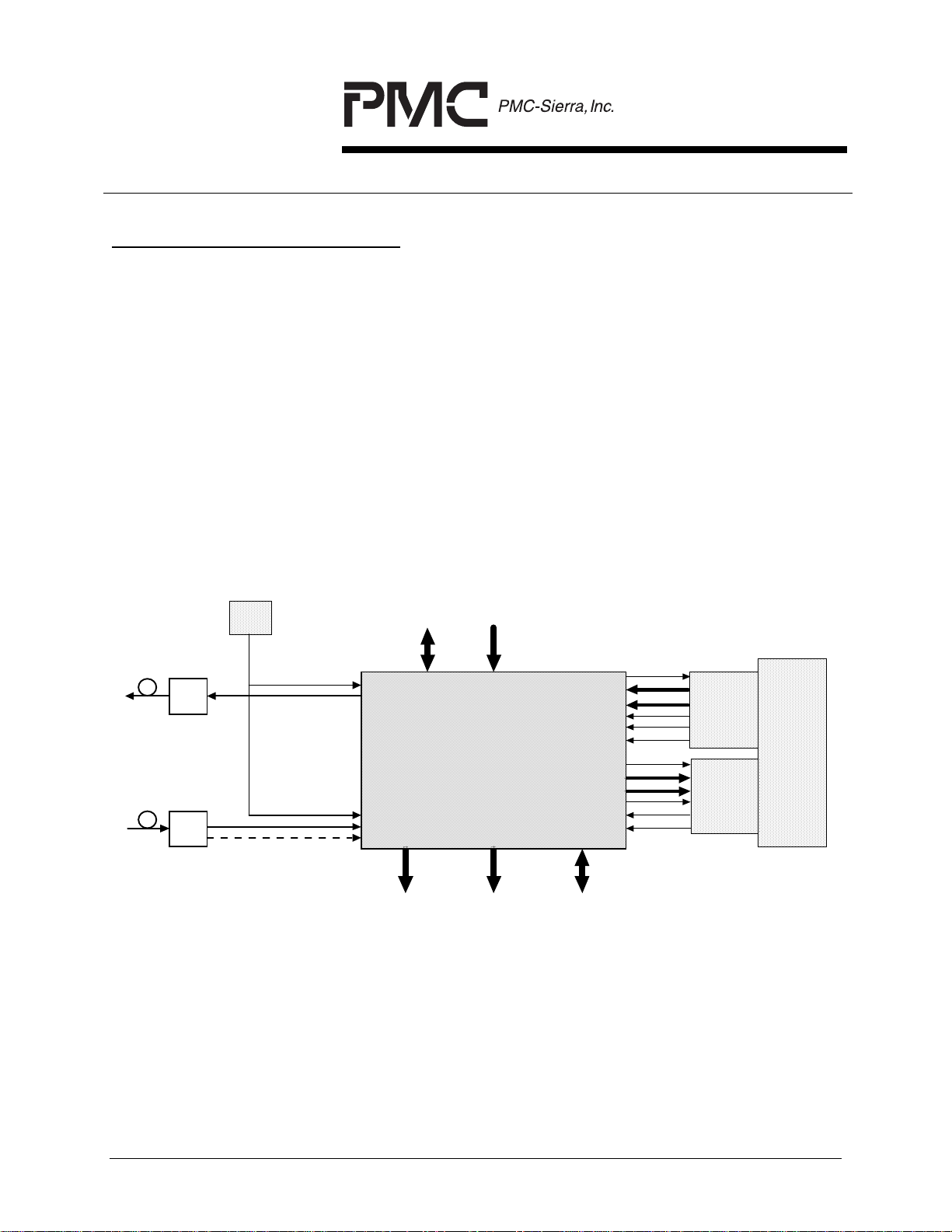
microprocessor interface. This application is shown in Figure 1.
Figure 1 - Typical STS-3c ATM Switch Port Interface
TRANSMIT
ALARM INSERT
SIGNALS
PM5347 S/UNI-PLUS
SONET/SDH
TCA
TXPRTY[1:0]
TDAT[15:0]
TSOC
TWRENB
TFCLK
RCA
RXPRTY[1:0]
RDAT[15:0]
RSOC
RRDENB
RFCLK
TRANSMIT
ATM
PROCESS
RECEIVE
ATM
PROCESS
SWITCHING
NETWORK
E/O
O/E
Ref.
Clock
19.44 MHz
TRCLK+/-
TXD+/-
RRCLK+/-
RXD+/-
ALOS+/-
TRANSMIT
OVERHEAD
INSERT
USER NETWORK INTERFACE
RECEIVE
OVERHEAD
EXTRACT
RECEIVE
ALARM DETECT
SIGNALS
MICRO BUS
FOR CONFIG, STATUS
AND CONTROL
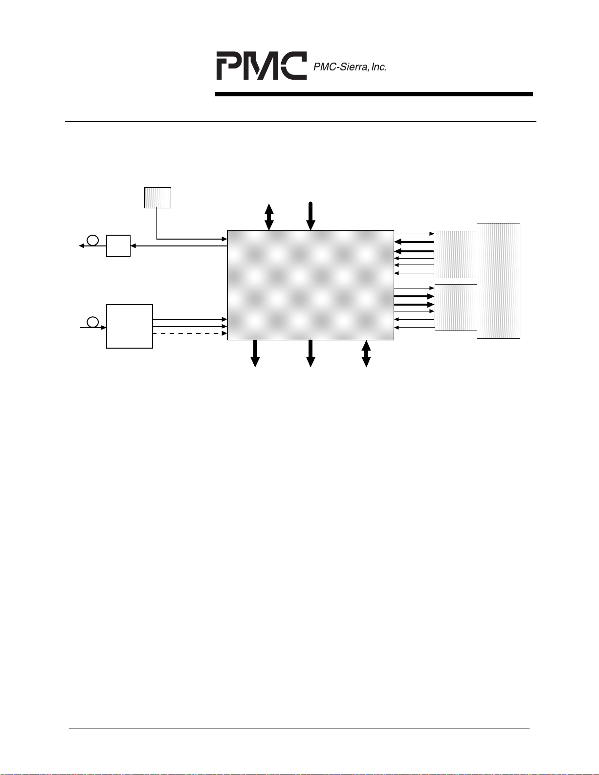
The clock recovery function of the S/UNI-PLUS may by bypassed. This is useful
in applications where clock recovery is not required such as when optical
receivers are utilized that have integral clock recovery. Similarly, the clock
synthesis function of the S/UNI-PLUS may be bypassed. This is useful in
applications where clock synthesis is not required, for example where a 155 MHz
transmit clock source is available. An example of an application where clock
recovery and clock synthesis are bypassed is shown in Figure 2.
PROPRIETARY AND CONFIDENTIAL TO PMC-SIERRA, INC., AND FOR ITS CUSTOMERS’ INTERNAL USE
7
Page 24
PM5347 S/UNI-PLUS
DATA SHEET
PMC-941033 ISSUE 6 SATURN USER NETWORK INTERFACE PLUS
Figure 2 - Application With Clock Recovery & Clock Synthesis
Bypassed
E/O
O/E
With
Clock
Recovery
Ref.
Clock
155.52 MHz
TRCLK+/-
TXD+/-
RRCLK+/-
RXD+/-
ALOS+/-
TRANSMIT
OVERHEAD
INSERT
TRANSMIT
ALARM INSERT
SIGNALS
PM5347 S/UNI-PLUS
SONET/SDH
USER NETWORK INTERFACE
RECEIVE
OVERHEAD
EXTRACT
RECEIVE
ALARM DETECT
SIGNALS
TCA
TXPRTY[1:0]
TDAT[15:0]
TSOC
TWRENB
TFCLK
RCA
RXPRTY[1:0]
RDAT[15:0]
RSOC
RRDENB
RFCLK
MICRO BUS
FOR CONFIG, STATUS
AND CONTROL
TRANSMIT
ATM
PROCESS
RECEIVE
ATM
PROCESS
SWITCHING
NETWORK
PROPRIETARY AND CONFIDENTIAL TO PMC-SIERRA, INC., AND FOR ITS CUSTOMERS’ INTERNAL USE
8
Page 25
PM5347 S/UNI-PLUS
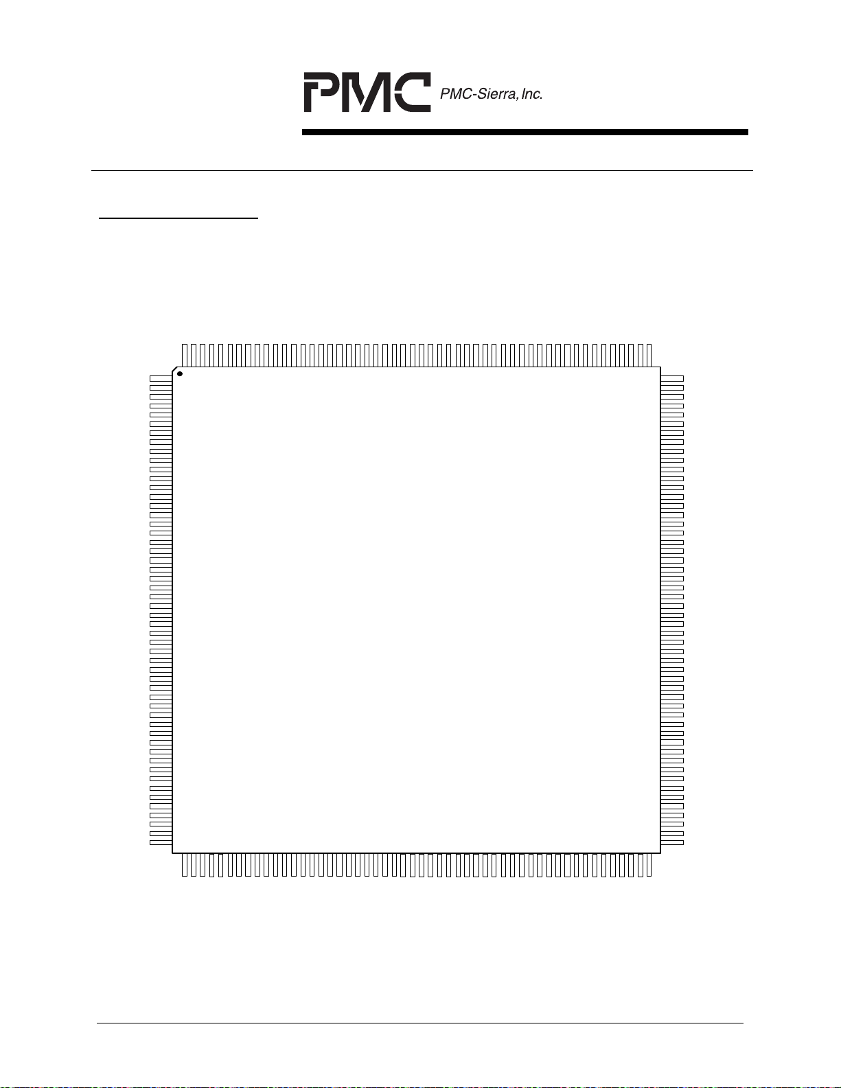
K
DATA SHEET
PMC-941033 ISSUE 6 SATURN USER NETWORK INTERFACE PLUS
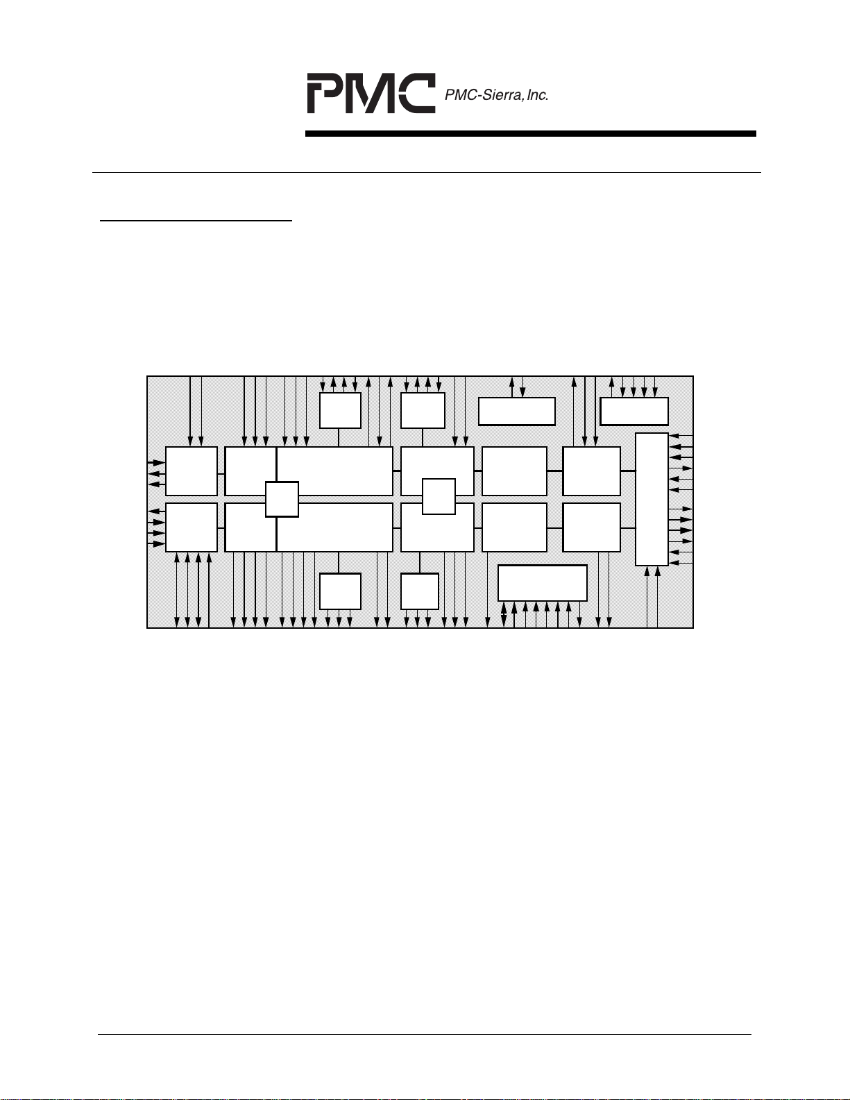
5
TRCLK+/-
TXD+/TXC+/-
RXDO+/-
RXD+/-
ALOS+/-
RRCLK+/-
BLOCK DIAG RAM
Normal Operating Mode
TLAIS
TSDCLK,TOWCL
TLDCLK
TATP
TBYP
Clock
Synthesizer
PISO
Clock
Recovery
SIPO
Section O/H
Processor
Section O/H
Processor
TLRDI
TSD,TSOW,TSUC
Tx
Section
Trace
Buffer
Rx
TLD,TLOW
TTOH
Transport
Insert
Line O/H
Processor
Rx
Line O/H
Processor
Transport
Extract
TTOHCLK
TTOHFP
O/H
Tx
O/H
TOHFP
TTOHEN
TFP
GTOCLK
TPOHCLK
TPOHFP
Path
O/H
Insert
Tx Path O/H
Processor
Path
Trace
Buffer
Rx Path O/H
Processor
Path
O/H
Extract
TPOHEN
TPAIS
TPRDI
POP[3:0]
Parallel
Input/Output Port
Tx ATM Cell
Processor
Rx ATM Cell
Processor
Microprocessor I/F
PIP[3:0]
TCP
XOFF
TGFC
Tx ATM
4 Cell
FIFO
Rx ATM
4 Cell
FIFO
TDO
TMS
TCK
TDI
JTAG Test
Access Port
Drop
Side
I/F
TRSTB
TSOC
TDAT[15:0]
TXPRTY[1:0]
TCA
TWRENB
TFCLK
RSOC
RDAT[15:0]
RXPRTY[1:0]
RCA
RRDENB
RFCLK
RBYP
LOF
LOS
RSD,RSOW,RSUC
RSDCLK,ROWCLK
LAIS
LRDI
RLDCLK
RTOH
RTOHFP
RTOHCLK
RLD,RLOW
ROHFP
GROCLK
RPOH TPOH
RPOHFP
LOP
PRDI
RPOHCLK
PAIS
LFO
LF+/-
RATP
LCD
A[7:0]
D[7:0]
ALE
CSB
RDB
WRB
INTB
RSTB
RCP
RGFC
TSEN
BUS8
PROPRIETARY AND CONFIDENTIAL TO PMC-SIERRA, INC., AND FOR ITS CUSTOMERS’ INTERNAL USE
9
Page 26
PM5347 S/UNI-PLUS
DATA SHEET
PMC-941033 ISSUE 6 SATURN USER NETWORK INTERFACE PLUS
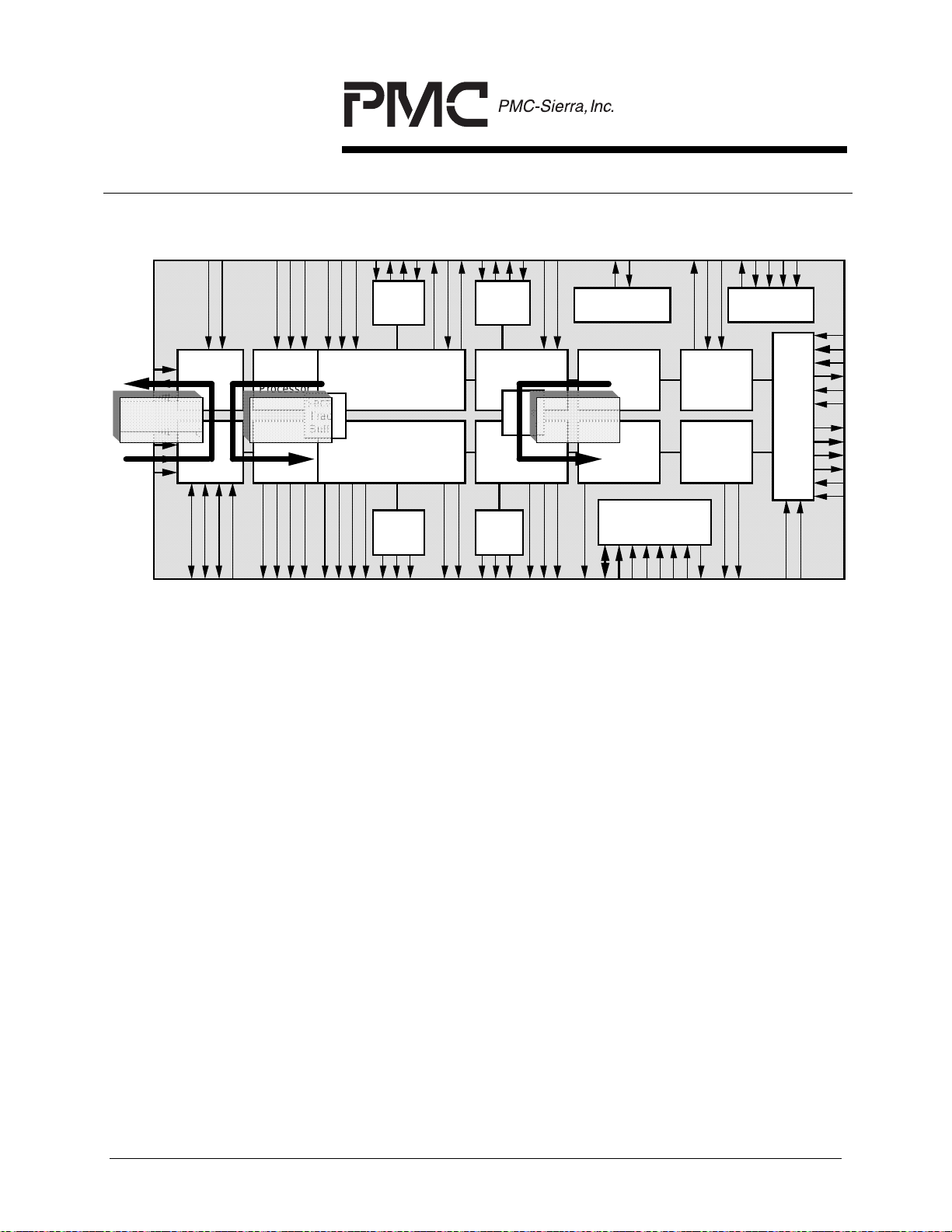
Loopback Modes
Synthesizer
SERIAL
LINE
LOOPBACK
Clock
PISO
Clock
Recovery
SIPO
Tx
Section O/H
Processor
DIAGNOSTIC
LOOPBACK
Section O/H
Processor
SERIAL
Rx
Section
Trace
Buffer
Transport
O/H
Insert
Tx
Line O/H
Processor
Rx
Line O/H
Processor
Transport
O/H
Extract
Path
O/H
Insert
Tx Path O/H
Processor
Path
Trace
Buffer
Rx Path O/H
Processor
Path
O/H
Extract
Parallel
Input/Output Port
Tx ATM Cell
Processor
PARALLEL
DIAGNOSTIC
LOOPBACK
Rx ATM Cell
Processor
Microprocessor I/F
Tx ATM
4 Cell
FIFO
Rx ATM
4 Cell
FIFO
JTAG Test
Access Port
Drop
Side
I/F
PROPRIETARY AND CONFIDENTIAL TO PMC-SIERRA, INC., AND FOR ITS CUSTOMERS’ INTERNAL USE
10
Page 27

PM5347 S/UNI-PLUS
DATA SHEET
PMC-941033 ISSUE 6 SATURN USER NETWORK INTERFACE PLUS
6
DESCRIPTION
The PM5347 S/UNI-PLUS SATURN User Network Interface is a monolithic
integrated circuit that implements the SONET/SDH processing and ATM mapping
functions of a 155 or 51 Mbit/s ATM User Network Interface.
The S/UNI-PLUS receives SONET/SDH streams using a bit serial interface,
recovers the clock and data and processes section, line, and path overhead. It
performs framing (A1, A2), descrambling, detects alarm conditions, and monitors
section, line, and path bit interleaved parity (B1, B2, B3), accumulating error
counts at each level for performance monitoring purposes. Line and path far end
block erro r indications (M0 or M1, G1) are also accumulated. The S/UNI-PLUS
interprets the received payload pointers (H1, H2) and extracts the synchronous
payload envelope which carries the received ATM cell payload. In addition to its
basic processing of the received SONET/SDH overhead, the S/UNI-PLUS
provides convenient access to all overhead bytes, which are extracted and
serialized on lower rate interfaces, allowing additional external processing of
overhead, if desired.
The S/UNI-PLUS frames to the ATM payload using cell delineation. HCS error
correction is provided. Idle/unassigned cells may be dropped according to a
programmable filter. Cells are also dropped upon detection of an uncorrectable
header check sequence error. The ATM cell payloads are descrambled. The
ATM cells that are passed are written to a four cell FIFO buffer. The received
cells are read from the FIFO using a generic 16- or 8-bit wide datapath interface.
Counts of received ATM cell headers that are errored and uncorrectable and also
those that are errored and correctable are accumulated independently for
performance monitoring purposes.
The S/UNI-PLUS transmits SONET/SDH streams using a bit serial interface and
formats section, line, and path overhead appropriately. It synthesizes the
transmit clock from a lower frequency reference and performs framing pattern
insertion (A1, A2), scrambling, alarm signal insertion, and creates section, line,
and path bit interleaved parity (B1, B2, B3) as required to allow performance
monitoring at the far end. Line and path far end block error indications (M0 or
M1, G1) are also inserted. The S/UNI-PLUS generates the payload pointer (H1,
H2) and inserts the synchronous payload envelope which carries the ATM cell
payload. In addition to its basic formatting of the transmitted SONET/SDH
overhead, the S/UNI-PLUS provides convenient access to all overhead bytes,
which are optionally inserted from lower rate serial interfaces, allowing external
sourcing of overhead, if desired. The S/UNI-PLUS also supports the insertion of
PROPRIETARY AND CONFIDENTIAL TO PMC-SIERRA, INC., AND FOR ITS CUSTOMERS’ INTERNAL USE
11
Page 28

PM5347 S/UNI-PLUS
DATA SHEET
PMC-941033 ISSUE 6 SATURN USER NETWORK INTERFACE PLUS
a large variety of errors into the transmit stream, such as framing pattern errors,
bit interleaved parity errors, and illegal pointers, which are useful for system
diagnostics and tester applications.
ATM cells are written to an internal four cell FIFO using a generic 16- or 8-bit
wide datapath interface. Idle/unassigned cells are automatically inserted when
the internal FIFO contains less than one cell. The S/UNI-PLUS provides
generation of the header check sequence and scrambles the payload of the ATM
cells. Each of these transmit ATM cell processing functions can be enabled or
bypassed.
No line rate clocks are required directly by the S/UNI-PLUS as it synthesizes the
transmit clock and recovers the receive clock using a 19.44 MHz or 6.48 MHz
reference clock. Optionally, receive clock recovery or transmit clock synthesis
may be bypassed.
The S/UNI-PLUS is configured, controlled and monitored via a generic 8-bit
microprocessor bus interface. The S/UNI-PLUS also provides a standard 5
signal IEEE 1149.1 JTAG test port for boundary scan board test purposes.
The S/UNI-PLUS is implemented in low power, +5 Volt, CMOS technology. It has
TTL and pseudo-ECL (PECL) compatible inputs and TTL/CMOS compatible
outputs and is packaged in a 208 pin PQFP package.
PROPRIETARY AND CONFIDENTIAL TO PMC-SIERRA, INC., AND FOR ITS CUSTOMERS’ INTERNAL USE
12
Page 29
PM5347 S/UNI-PLUS
DATA SHEET
PMC-941033 ISSUE 6 SATURN USER NETWORK INTERFACE PLUS
7
PIN DIAG RAM
The S/UNI-PLUS is packaged in a 208 pin plastic QFP package having a body
size of 28 mm by 28 mm and a pin pitch of 0.5 mm.
PIN 1
RDAT[9]
RDAT[10]
RDAT[11]
VDD_AC
VSS_AC
RDAT[12]
VDD_DC
VSS_DC
RDAT[13]
RDAT[14]
RDAT[15]
A[0]
A[1]
A[2]
A[3]
A[4]
A[5]
A[6]
A[7]
ALE
RSTB
CSB
WRB
RDB
INTB
TRSTB
D[0]
D[1]
VDD_DC
VSS_DC
D[2]
D[3]
VDD_AC
VSS_AC
D[4]
D[5]
VDD_DC
VSS_DC
D[6]
D[7]
TDO
TDI
TMS
TSEN
BUS8
TCK
TDAT[0]
TDAT[1]
TDAT[2]
TDAT[3]
TDAT[4]
TDAT[5]
PIN 52
VSS_DC
RDAT[8]
PIN 208
Index
RDAT[7]
VDD_DC
RDAT[6]
RDAT[5]
RDAT[4]
VSS_AC
RDAT[3]
VDD_AC
VSS_DC
RDAT[2]
VDD_DC
RDAT[0]
RDAT[1]
RXPRTY[1]
RRDENB
RXPRTY[0]
RFCLK
RSOC
VSS_AC
RCA
GROCLK
LOS
LOF
LOP
VDD_AC
LCD
PM5347
S/UNI-PLUS
PAIS
PRDI
VSS_DC
LAIS
VDD_DC
LRDI
RCP
RGFC
ROHFP
RPOH
RPOHFP
RTOHFP
RTOH
RPOHCLK
RTOHCLK
VDD_AC
VSS_AC
RSOW
RSUC
RLD
VSS_DC
VDD_DC
RLDCLK
RSD
PIN 157
PIN 156
RSDCLK
ROWCLK
RLOW
RBYP
RATP
LF+
LFLFO
RAVS1
RAVD1
RAVS2
RAVD2
RAVS4
RRCLKRRCLK+
RAVD4
RAVD3
RAVS3
ALOSALOS+
RXDRXD+
VSS_AC
VDD_AC
RXDORXDO+
VSS_DC
VDD_DC
TXVSS
TXDTXD+
TXCTXC+
TXVDD
TAVS3
TRCLKTRCLK+
TAVD3
TAVS2
TAVD2
TAVS1
TAVD1
TATP
TBYP
PIP[0]
PIP[1]
PIP[2]
PIP[3]
POP[0]
POP[1]
POP[2]
POP[3]
PIN 105
TDAT[6]
TDAT[7]
PIN 53
TDAT[8]
TDAT[9]
TDAT[12]
TDAT[10]
TDAT[11]
VSS_DC
TDAT[13]
VDD_DC
TDAT[14]
TDAT[15]
TXPRTY[0]
TSOC
TFCLK
TWRENB
TXPRTY[1]
TCA
XOFF
GTOCLK
TPAIS
TPRDI
TLAIS
TLRDI
TCP
TGFC
TFP
VSS_DC
VDD_DC
TOHFP
VSS_AC
VDD_AC
TPOH
TPOHFP
TPOHEN
TPOHCLK
TTOH
TTOHFP
TSOW
TTOHEN
TTOHCLK
TSUC
TLOW
TOWCLK
VSS_DC
VDD_DC
VDD_AC
TLD
VSS_AC
PROPRIETARY AND CONFIDENTIAL TO PMC-SIERRA, INC., AND FOR ITS CUSTOMERS’ INTERNAL USE
TSD
TSDCLK
TLDCLK
PIN 104
13
Page 30

PM5347 S/UNI-PLUS
DATA SHEET
PMC-941033 ISSUE 6 SATURN USER NETWORK INTERFACE PLUS
8
PIN DESCRIPTION
Pin Name Type Pin
Function
No.
RBYP Input 153 The receive bypass (RBYP) input disables clock
recovery. If RBYP is high, RXD+/- is sampled on
the rising edge of RRCLK+/-. If RBYP is low, the
receive clock is recovered from the RXD+/- bit
stream. RBYP requires an external pull-down
resistor.
RXD+
RXD-
PECL
Input
135
136
The receive differential data inputs (RXD+, RXD-)
contain the NRZ bit serial receive stream. RXD+/-
is sampled on the rising edge of RRCLK+/- when
clock recovery is bypassed (the falling edge may
be used by reversing RRCLK+/-), otherwise the
receive clock is recovered from the RXD+/- bit
stream. Please refer to the Operation section for
a discussion of PECL interfacing issues.
RXDO+
RXDO-
Output 131
132
The receive differential data outputs (RXDO+,
RXDO-) are sliced versions of the RXD+ and
RXD- inputs. These outputs are provided to allow
decision feedback equalization (DFE) to correct
baseline wander. It is intended that these outputs
be low pass filtered and attenuated to create an
appropriate correction signal that is summed with
incoming data to recover the low frequency
components.
RRCLK+
RRCLK-
PECL
Input
142
143
The receive differential reference clock inputs
(RRCLK+, RRCLK-) must be a jitter-free 19.44
MHz or 6.48 MHz reference clock when clock
recovery is enabled. When clock recovery is
bypassed, RRCLK+/- is nominally a 155.52 MHz
or 51.84 MHz 50% duty cycle clock and provides
timing for the S/UNI-PLUS receive functions. In
this case, RXD+/- is sampled on the rising edge of
RRCLK+/-. Please refer to the Operation section
for a discussion of PECL interfacing issues.
PROPRIETARY AND CONFIDENTIAL TO PMC-SIERRA, INC., AND FOR ITS CUSTOMERS’ INTERNAL USE
14
Page 31

PM5347 S/UNI-PLUS
DATA SHEET
PMC-941033 ISSUE 6 SATURN USER NETWORK INTERFACE PLUS
Pin Name Type Pin
Function
No.
ALOS+
ALOS-
PECL
Input
137
138
The analog loss of signal (ALOS+/-) differential
inputs are used to indicate a loss of receive signal
power. When ALOS+/- is asserted, the data on
the receive data (RXD+/-) pins is forced to all
zeros and the phase locked loop switches to the
reference clock (RRCLK+/-) to keep the recovered
clock in range. These inputs must be DC coupled.
Please refer to the Operation section for a
discussion of PECL interfacing issues.
RATP Analog 152 This analog test point (RATP) is provided for
production test purposes. Connect this pin to
ground.
LF+,
LF-,
LFO
Analog 151
150
149
Passive components connected to the recovery
loop filter (LF+, LF- and LFO) pins determine the
dynamics of the clock recovery unit. Refer to the
Operation section for details.
TBYP Input 113 If the transmit bypass (TBYP) input is high,
transmit clock synthesis is disabled and TRCLK+/-
becomes the line rate clock of 155.52 MHz or
51.84 MHz. If TBYP is low, the transmit clock is
synthesized from a 19.44 MHz or 6.48 MHz
reference. TBYP requires an external pull down
resistor.
TRCLK+
TRCLK-
PECL
Input
120
121
The transmit differential reference clock inputs
(TRCLK+, TRCLK-) must be a jitter-free 19.44
MHz or 6.48 MHz reference clock when clock
synthesis is enabled. When clock synthesis is
bypassed, TRCLK+/- is nominally a 155.52 MHz
or 51.84 MHz 50% duty cycle clock. This clock
provides timing for the S/UNI-PLUS transmit
functions. TRCLK+/- may be left unconnected
when S/UNI-PLUS loop timing is enabled, or
when the transmit clock is synthesized from the
receive reference (RRCLK+/-). Please refe r to the
Operation section for a discussion of PECL
interfacing issues.
PROPRIETARY AND CONFIDENTIAL TO PMC-SIERRA, INC., AND FOR ITS CUSTOMERS’ INTERNAL USE
15
Page 32

PM5347 S/UNI-PLUS
DATA SHEET
PMC-941033 ISSUE 6 SATURN USER NETWORK INTERFACE PLUS
Pin Name Type Pin
Function
No.
TXD+
TXD-
TXC+
TXC-
Output 126
127
Output 124
125
The transmit differential data outputs (TXD+, TXD-
) contain the transmit stream. TXD+/- is updated
on the falling edge of TXC+/-
The transmit clock (TXC+, TXC-) outputs are
available when the transmit data rate is 51.84
Mbit/s. TXD+/- is updated on the falling edge of
TXC+ and on the rising edge of TXC-. When
STS-3c (STM-1) is selected, TXC+ is held low and
TXC- is held high.
TATP Analog 114 This analog test point (TATP) is provided for
production test purposes. Connect this pin to
ground.
GROCLK Output 187 The generated receive clock (GROCLK) is
nominally a 6.48 MHz or 19.44 MHz, 50% duty
cycle clock. Receive outputs that are timed from
the line are updated with timing aligned to
GROCLK.
When configured for receive clock recovery
(RBYP low), GROCLK is the recovered line clock
divided down by 8.
When receive clock recovery is bypassed (RBYP
high), GROCLK is equal to RRCLK+/- divided
down by 8.
PROPRIETARY AND CONFIDENTIAL TO PMC-SIERRA, INC., AND FOR ITS CUSTOMERS’ INTERNAL USE
16
Page 33

PM5347 S/UNI-PLUS
DATA SHEET
PMC-941033 ISSUE 6 SATURN USER NETWORK INTERFACE PLUS
Pin Name Type Pin
Function
No.
TFP Input 81 The active high transmit frame pulse (TFP) signal
is used to align the SONET/SDH transport frame
generated by the S/UNI-PLUS device to a system
reference. TFP should be brought high for a
single GTOCLK period every 810 (STS-1), or
2430 (STS-3c/STM-1) GTOCLK cycles or a
multiple thereof. TFP may be tied low if such
synchronization is not required. The offset
between an active TFP input and the resultant
frame alignment on TOHFP is 16 GTOCLK
periods in STS-1 mode and 24 GTOCLK periods
in STS-3c mode. TFP is sampled on the rising
edge of GTOCLK.
GTOCLK Output 72 The generated transmit output clock (GTOCLK) is
nominally a 6.48 MHz or 19.44 MHz, 50% duty
cycle clock. Transmit inputs and outputs that are
timed from the line are updated with timing
aligned to GTOCLK.
When configured for transmit clock synthesis
(TBYP low), GTOCLK is the synthesized line clock
divided by 8.
When transmit clock synthesis is bypassed (TBYP
high), GTOCLK is equal to TRCLK+/- divided by 8.
TOHFP Output 84 The transmit overhead frame pulse (TOHFP)
signal identifies the start of a byte on outputs
TSOW, TSUC and TLOW. If required, TOHFP is
one GTOCLK clock cycle wide and can be used
as a reset pulse for an external counter. Please
refer to the functional timing diagrams for details.
PROPRIETARY AND CONFIDENTIAL TO PMC-SIERRA, INC., AND FOR ITS CUSTOMERS’ INTERNAL USE
17
Page 34

PM5347 S/UNI-PLUS
DATA SHEET
PMC-941033 ISSUE 6 SATURN USER NETWORK INTERFACE PLUS
Pin Name Type Pin
Function
No.
LOS Output 186 The loss of signal (LOS) signal is set high when
loss of signal is declared. This occurs when a
violating period (20 ± 3 µs) of consecutive all
zeros bytes is detected on the incoming STS-3c/1
(STM-1) signal (before descrambling). LOS is
removed when two valid framing words (A1, A2)
are detected and during the intervening time, no
violating period of consecutive all zeros patter n s
is detected. This alarm indication is also available
via register access. LOS is updated on the falling
edge of GROCLK.
LOF Output 185 The loss of frame (LOF) signal is set high when
loss of frame is declared. This occurs when an
out-of-frame condition persists for a period of 3
ms. LOF is removed when an in-frame condition
persists for a period of 3 ms. This alarm indication
is also available via register access. LOF is
updated on the falling edge of GROCLK.
LAIS Output 176 The line alarm indication signal (LAIS) is set high
when line AIS is declared. This occurs when a
111 binary pattern is detected in bits 6, 7, and 8
of the K2 byte for three or five consecutive frames
(as selected in the RLOP Control/Status register).
LAIS is removed when any pattern other than 111
is detected in bits 6, 7, and 8 of the K2 byte for
three or five consecutive frames. This alarm
indication is also available via register access.
LAIS is updated on the falling edge of GROCLK.
PROPRIETARY AND CONFIDENTIAL TO PMC-SIERRA, INC., AND FOR ITS CUSTOMERS’ INTERNAL USE
18
Page 35

PM5347 S/UNI-PLUS
DATA SHEET
PMC-941033 ISSUE 6 SATURN USER NETWORK INTERFACE PLUS
Pin Name Type Pin
Function
No.
LRDI Output 175 The line remote defect indication (LRDI) signal is
set high when line RDI is declared. This occurs
when a 110 binary pattern is detected in bits 6, 7,
and 8 of the K2 byte for three or five consecutive
frames (as selected in the RLOP Control/Status
register). LRDI is removed when any pattern
other than 110 is detected in bits 6, 7, and 8 of
the K2 byte for three or five consecutive frames.
This alarm indication is also available via register
access. LRDI is updated on the falling edge of
GROCLK.
LOP Output 182 The loss of pointer (LOP) signal is set high when
loss of pointer is declared. This occurs when a
valid pointer (H1, H2) is not found in eight
consecutive frames, or if eight consecutive new
data flags are detected. LOP is removed when
the same valid and normal pointer with a normal
new data flag is detected in three consecutive
frames. The loss of pointer state is not entered if
the receive stream contains path AIS. This alarm
indication is also available via register access.
LOP is updated on the falling edge of GROCLK.
PAIS Output 180 The path AIS (PAIS) signal is set high when path
AIS is declared. This occurs when an all ones
pattern is observed in the pointer bytes (H1, H2)
for three consecutive frames. Path AIS is
removed when the same valid and normal pointer
is detected for three consecutive frames or a legal
pointer with an active new data flag (NDF) is
received. This alarm indication is also available
via register access. PAIS is updated on the falling
edge of GROCLK.
PROPRIETARY AND CONFIDENTIAL TO PMC-SIERRA, INC., AND FOR ITS CUSTOMERS’ INTERNAL USE
19
Page 36

PM5347 S/UNI-PLUS
DATA SHEET
PMC-941033 ISSUE 6 SATURN USER NETWORK INTERFACE PLUS
Pin Name Type Pin
Function
No.
PRDI Output 179 The path remote defect indication (PRDI) signal is
set high when path RDI is declared. This occurs
when bit 5 of the path status byte (G1) is set high
for five or ten consecutive frames. Path RDI is
removed when bit 5 of the G1 byte is set low for
five or ten consecutive frames (as selected in the
RPOP Pointer MSB and RDI Filter Control
register). This alarm indication is also available
via register access. PRDI is updated on the falling
edge of GROCLK.
LCD Output 181 The loss of cell delineation (LCD) signal indicates
when cell delineation can not be found. LCD
transitions high when an out of cell delineation
(OCD) anomaly has persisted for 4 ms. Once
asserted, LCD remains high until no OCD
anomaly has been detected for 4 ms at which
time, LCD is set low. The OCD state is entered
when the cell delineation state machine is not in
the SYNC state. Please refer to the Functional
Description section for an explanation of the cell
delineation state machine.
This alarm indication is also available via register
access. LCD is updated on the falling edge of
GROCLK.
TLAIS Input 75 The active high transmit line alarm indication
(TLAIS) signal controls the insertion of line AIS.
Line AIS is inserted by overwriting the
SONET/SDH frame contents with all ones (before
scrambling). The section overhead is not
overwritten. This function can also be performed
via register access. Line AIS insertion is internally
synchronized to frame boundaries. The TLAIS
input takes precedence over the TTOH and
TTOHEN inputs. TLAIS is sampled on the rising
edge of GTOCLK.
PROPRIETARY AND CONFIDENTIAL TO PMC-SIERRA, INC., AND FOR ITS CUSTOMERS’ INTERNAL USE
20
Page 37

PM5347 S/UNI-PLUS
DATA SHEET
PMC-941033 ISSUE 6 SATURN USER NETWORK INTERFACE PLUS
Pin Name Type Pin
Function
No.
TLRDI Input 76 The active high transmit line remote defect
indication (TLRDI) signal controls the insertion of
line RDI. Line RDI is inserted by transmitting the
code 110 (binary) in bit positions 6, 7, and 8 of the
K2 byte. This function can also be performed via
register access, or be enabled to occur
automatically upon detection of receive line AIS,
loss of signal, or loss of frame. The TLRDI input
takes precedence over the TTOH and TTOHEN
inputs. TLRDI is sampled on the rising edge of
GTOCLK.
TPAIS Input 73 The active high transmit path alarm indication
(TPAIS) signal controls the insertion of STS-path
AIS. A high level on TPAIS forces the insertion of
an all ones pattern into the complete synchronous
payload envelope, and the payload pointer bytes
(H1, H2). Path AIS insertion is internally
synchronized to SPE frame boundaries. This
function can also be performed via register
access. TPAIS is sampled on the rising edge of
GTOCLK.
TPRDI Input 74 The transmit path remote defect indication
(TPRDI) signal controls the insertion of path RDI.
A high level on TPRDI forces a logic one to be
inserted in the path RDI bit position in the path
status byte (G1). This function can also be
performed via register access, or be enabled to
occur automatically upon detection of receive line
AIS, loss of frame, loss of signal, loss of pointer,
or path AIS. The TPOH and TPOHEN inputs take
precedence over the TPRDI input. TPRDI is
sampled on the rising edge of GTOCLK.
PROPRIETARY AND CONFIDENTIAL TO PMC-SIERRA, INC., AND FOR ITS CUSTOMERS’ INTERNAL USE
21
Page 38

PM5347 S/UNI-PLUS
DATA SHEET
PMC-941033 ISSUE 6 SATURN USER NETWORK INTERFACE PLUS
Pin Name Type Pin
Function
No.
RFCLK Input 191 The receive FIFO clock (RFCLK) is used to read
words from the synchronous FIFO interface.
RFCLK must cycle at a 52 MHz or lower
instantaneous rate, but at a high enough rate to
avoid FIFO overflow. RRDENB is sample d using
the rising edge of RFCLK. RSOC, RCA,
RXPRTY[1:0] and RDAT[15:0] are updated on the
rising edge of RFCLK.
RRDENB Input 190 The active low receive read enable input
(RRDENB) is used to initiate reads from the
receive FIFO. When sampled low using the rising
edge of RFCLK, a word is read from the internal
synchronous FIFO and output on bus RDAT[15:0].
When sampled high using the rising edge of
RFCLK, no read is performed and outputs
RDAT[15:0], RXPRTY[1:0] and RSOC are tristated
if the TSEN input is high. RRDENB must operate
in conjunction with RFCLK to access the FIFO at
a high enough instantaneous rate as to avoid
FIFO overflows.
PROPRIETARY AND CONFIDENTIAL TO PMC-SIERRA, INC., AND FOR ITS CUSTOMERS’ INTERNAL USE
22
Page 39

PM5347 S/UNI-PLUS
DATA SHEET
PMC-941033 ISSUE 6 SATURN USER NETWORK INTERFACE PLUS
Pin Name Type Pin
No.
RDAT[0]
RDAT[1]
RDAT[2]
RDAT[3]
RDAT[4]
RDAT[5]
RDAT[6]
RDAT[7]
RDAT[8]
RDAT[9]
RDAT[10]
RDAT[11]
RDAT[12]
Tristate 194
195
196
199
202
203
204
205
208
1
2
3
6
Function
The receive cell data (RDAT[15:0]) bus carries the
ATM cell octets that are read from the receive
FIFO. When the 16-bit SCI-PHY interface is
selected, (BUS8 is tied low), RDAT[15:0] contains
the 16 bit wide word bus. When the 8-bit SCI-
PHY interface is sele cted (BUS8 is tied high),
RDAT[7:0] contains the 8-bit wide word bus
(RDAT[15:8] is not used). RDAT[15:0] is updated
on the rising edge of RFCLK.
When the S/UNI-PLUS is configured for tristate
operation using the TSEN input, tristating of
output bus RDAT[15:0] is controlled by input
RRDENB.
RDAT[13]
RDAT[14]
RDAT[15]
RXPRTY[0]
RXPRTY[1]
9
10
11
Tristate 192
193
The receive parity (RXPRTY[1:0]) signals indicate
the parity of the RDAT[15:0] bus. RXPRTY[1] is
the parity calculation over the RDAT[15:8] bus.
RXPRTY[0] is the parity calculation over the
RDAT[7:0] bus. Alternately, the device can be
configured so that RXPRTY[1] is the parity
calculation over the entire RDAT[15:0] bus.
RXPRTY[0] is not used in this case. Odd or even
parity selection can be made using the RACP
Control register. RXPRTY[1:0] is updated on the
rising edge of RFCLK.
When the S/UNI-PLUS is configured for tristate
operation using the TSEN input, tristating of
output bus RXPRTY[1:0] is control by input
RRDENB.
PROPRIETARY AND CONFIDENTIAL TO PMC-SIERRA, INC., AND FOR ITS CUSTOMERS’ INTERNAL USE
23
Page 40

PM5347 S/UNI-PLUS
DATA SHEET
PMC-941033 ISSUE 6 SATURN USER NETWORK INTERFACE PLUS
Pin Name Type Pin
Function
No.
RSOC Tristate 189 The receive start of cell (RSOC) signal marks the
start of cell on the RDAT[15:0] bus. When RSOC
is high, the first word of the cell structure is
present on the RDAT[15:0] bus. RSOC is updated
on the rising edge of RFCLK.
When the S/UNI-PLUS is configured for tristate
operation using the TSEN input, tristating of
output RSOC is control by input RRDENB.
RCA Output 188 The receive cell available (RCA) signal indicates
when a cell is available in the receive FIFO. When
asserted, RCA indicates that the receive FIFO
has at least one cell available to be read. When
RCA is deasserted, the receive FIFO contains
only four words or is empty (as selected in the
RACP Interrupt Enable/Control register). RCA
default state can be selected in the S/UNI-PLUS
Master Control register. RCA is updated on the
rising edge of RFCLK. The active polarity of this
signal is programmable and defaults to active
high.
BUS8 Input 45 The bus width select (BUS8) input selects the
transmit and receive SCI-PHY interface types.
When BUS8 is tied high, the 8-bit wide SCI-PHY
interface is enabled. When BUS8 is tied low, the
16-bit wide SCI-PHY interface is selected.
TSEN Input 44 The tristate enable (TSEN) signal allows tristate
control over outputs RDAT[15:0], RXPRTY[1:0]
and RSOC. When TSEN is high, the active low
receive read enable input, RRBENB controls
when outputs RDAT[15:0], RXPRTY[1:0] and
RSOC are driven. When TSEN is low, outputs
RDAT[15:0], RXPRTY[1:0] and RSOC are always
driven.
PROPRIETARY AND CONFIDENTIAL TO PMC-SIERRA, INC., AND FOR ITS CUSTOMERS’ INTERNAL USE
24
Page 41

PM5347 S/UNI-PLUS
DATA SHEET
PMC-941033 ISSUE 6 SATURN USER NETWORK INTERFACE PLUS
Pin Name Type Pin
Function
No.
TFCLK Input 67 The transmit FIFO clock (TFCLK) is used to write
words to the synchronous FIFO interface. TFCLK
must cycle at a 52 MHz or lower instantaneous
rate. TWRENB, TSOC, TXPRTY[1:0] and
TDAT[15:0] are sampled on the rising edge of
TFCLK. In addition, TCA is updated on the rising
edge of TFCLK.
TWRENB Input 68 The active low transmit write enable input
(TWRENB) is used to initiate writes to the transmit
FIFO. When sampled low using the rising edge of
TFCLK, the 16-bit word on TDAT[15:0] is written
into the transmit FIFO. When sampled high using
the rising edge of TFCLK, no write is performed.
A complete 53 octet cell must be written to the
FIFO before it is inserted into the STS-3c/1 (STM-
1) SPE. Idle/unassigned cells are inserted when
a complete cell is not available.
PROPRIETARY AND CONFIDENTIAL TO PMC-SIERRA, INC., AND FOR ITS CUSTOMERS’ INTERNAL USE
25
Page 42

PM5347 S/UNI-PLUS
DATA SHEET
PMC-941033 ISSUE 6 SATURN USER NETWORK INTERFACE PLUS
Pin Name Type Pin
No.
TDAT[0]
TDAT[1]
TDAT[2]
TDAT[3]
TDAT[4]
TDAT[5]
TDAT[6]
TDAT[7]
TDAT[8]
TDAT[9]
TDAT[10]
TDAT[11]
TDAT[12]
Input 47
48
49
50
51
52
53
54
55
56
57
58
59
Function
The transmit cell data (TDAT[15:0]) bus carries the
ATM cell octets that are written to the transmit
FIFO. When the 16-bit SCI-PHY interface is
selected, (BUS8 is tied low), TDAT[15:0] contains
the 16-bit wide word bu s. When the 8-bit SCI-
PHY interface is sele cted (BUS8 is tied high),
TDAT[7:0] contains the 8-bit wide word bus
(TDAT[15:8] is not used). TDAT[15:0] is sampled
on the rising edge of TFCLK and is considered
valid only when TWRENB is simultaneously
asserted.
TDAT[13]
TDAT[14]
TDAT[15]
TXPRTY[0]
TXPRTY[1]
62
63
64
Input 65
66
The transmit parity (TXPRTY[1:0]) signals indicate
the parity of the TDAT[15:0] bus. TXPRTY[1] is
expected to be the parity calculation over the
TDAT[15:8] bus. TXPRTY[0] is expected to be the
parity calculation over the TDAT[7:0] bus.
Alternately, the device can be configured so that
TXPRTY[1] is expected to be the parity calculation
over the entire TDAT[15:0] bus. TXPRTY[0]
should be tied low in this case. Odd or even parity
selection can be made using the TACP FIFO
Control register. TXPRTY[1:0] is sampled on the
rising edge of TFCLK and is considered valid only
when TWRENB is simultaneously asserted.
PROPRIETARY AND CONFIDENTIAL TO PMC-SIERRA, INC., AND FOR ITS CUSTOMERS’ INTERNAL USE
26
Page 43

PM5347 S/UNI-PLUS
DATA SHEET
PMC-941033 ISSUE 6 SATURN USER NETWORK INTERFACE PLUS
Pin Name Type Pin
Function
No.
TSOC Input 69 The transmit start of cell (TSOC) signal marks the
start of cell on the TDAT[15:0] bus. When TSOC is
high, the first word of the cell structure is present
on the TDAT[15:0] bus. It is not necessary for
TSOC to be present at each cell. An interrupt
may be generated if TSOC is high during any
word other than the first word of the cell structure.
TSOC is sampled on the rising edge of TFCLK
and is considered valid only when TWRENB is
simultaneously asserted.
TCA Output 70 The transmit cell available (TCA) signal indicates
when a cell is available in the transmit FIFO.
When asserted, TCA indicates that the transmit
FIFO is not full. When TCA is deasserted, it
indicates that either the transmit FIFO is near full
and can accept no more than four writes or that
the transmit FIFO is full (as selected in the TACP
FIFO Control register) In addition, to reduce FIFO
latency, the FIFO full level can be programmed in
the TACP FIFO Control register. The default state
of TCA can be selected in the S/UNI-PLUS
Master Control register. TCA is updated on the
rising edge of TFCLK. The active polarity of this
signal is programmable and defaults to active
high.
XOFF Input 71 The transmit off (XOFF) input prevents the
insertion of cells from the transmit FIFO. If XOFF
is set high, the next cell transmitted is an
idle/unassigned cell regardless of the number of
cells in the FIFO. Idle/unassigned cells are
transmitted until XOFF is deasserted. XOFF may
be treated as an asynchronous signal. XOFF
must be tied low if it is not used.
PROPRIETARY AND CONFIDENTIAL TO PMC-SIERRA, INC., AND FOR ITS CUSTOMERS’ INTERNAL USE
27
Page 44

PM5347 S/UNI-PLUS
DATA SHEET
PMC-941033 ISSUE 6 SATURN USER NETWORK INTERFACE PLUS
Pin Name Type Pin
Function
No.
RTOH Output 168 The receive transport overhead output (RTOH)
contains the receive transport overhead bytes
(A1, A2, J0/Z0, B1, E1, F1, D1-D3, H1-H3, B2,
K1, K2, D4-D12, S1/Z1, M0 or M1/Z2, and E2)
extracted from the receive stream. RTOH is
updated on the falling edge of RTOHCLK.
RTOHCLK Output 164 The receive transport overhead clock (RTOHCLK)
is nominally a 5.184 MHz clock (STM-1/STS-3c)
or a 1.728 MHz clock (STS-1) which provides
timing to process the extracted receive transport
overhead. When STS-3c (STM-1) mode is
selected, RTOHCLK is a gapped 6.48 MHz clock.
When STS-1 mode is selected, RTOHCLK is a
gapped 2.16 MHz clock. RTOHCLK is updated on
the falling edge of GROCLK.
RTOHFP Output 167 The receive transport overhead frame position
(RTOHFP) signal is used to locate the individual
receive transport overhead bits in the transport
overhead output, RTOH. RTOHFP is set high
while bit 1 (the most significant bit) of the first
framing byte (A1) is present in the RTOH stream.
RTOHFP is updated on the falling edge of
RTOHCLK.
RPOH Output 171 The receive path overhead data (RPOH) signal
contains the path overhead bytes (J1, B3, C2, G1,
F2, H4, Z3, Z4, and Z5) extracted from the
received STS-3c/1 frame. RPOH is updated on
the falling edge of RPOHCLK.
RPOHCLK Output 169 The receive path overhead clock (RPOHCLK) is
nominally a 576 kHz clock which provides timing
to process the extracted receive path overhead.
RPOHCLK is a gapped 648 KHz clock.
RPOHCLK is updated on the falling edge of
GROCLK.
PROPRIETARY AND CONFIDENTIAL TO PMC-SIERRA, INC., AND FOR ITS CUSTOMERS’ INTERNAL USE
28
Page 45

PM5347 S/UNI-PLUS
DATA SHEET
PMC-941033 ISSUE 6 SATURN USER NETWORK INTERFACE PLUS
Pin Name Type Pin
Function
No.
RPOHFP Output 170 The receive path overhead frame position
(RPOHFP) signal may be used to locate the
individual receive path overhead bits in the path
overhead data stream, RPOH. RPOHFP is logic
one while bit 1 (the most significant bit) of the path
trace byte (J1) is present in the RPOH stream.
RPOHFP is updated on the falling edge of
RPOHCLK.
RSDCLK Output 156 The receive section DCC clock (RSDCLK) is a
192 kHz clock used to update the RSD output.
RSDCLK is generated by gapping a 216 kHz
clock.
RSD Output 157 The receive section DCC (RSD) signal contains
the serial section data communications channel
(D1, D2, D3) extracted from the receive stream.
RSD is updated on the falling edge of RSDCLK.
RLDCLK Output 158 The receive line DCC clock (RLDCLK) is a 576
kHz clock used to update the RLD output.
RLDCLK is generated by gapping a 2.16 MHz
clock.
RLD Output 159 The receive line DCC (RLD) signal contains the
serial line data communications channel (D4 -
D12) extracted from the receive stream. RLD is
updated on the falling edge of RLDCLK.
ROWCLK Output 155 The receive orderwire clock (ROWCLK) is a 64
kHz clock used to update the RSOW, RSUC, and
RLOW outputs. ROWCLK is generated by
gapping a 72 kHz clock.
RSOW Output 163 The receive section orderwire (RSOW) signal
contains the section orderwire channel (E1)
extracted from the receive stream. RSOW is
updated on the falling edge of ROWCLK.
PROPRIETARY AND CONFIDENTIAL TO PMC-SIERRA, INC., AND FOR ITS CUSTOMERS’ INTERNAL USE
29
Page 46

PM5347 S/UNI-PLUS
DATA SHEET
PMC-941033 ISSUE 6 SATURN USER NETWORK INTERFACE PLUS
Pin Name Type Pin
Function
No.
RSUC Output 162 The receive section user channel (RSUC) signal
contains the section user channel (F1) extracted
from the receive stream. RSUC is updated on the
falling edge of ROWCLK.
RLOW Output 154 The receive line orderwire (RLOW) signal contains
the line orderwire channel (E2) extracted from the
receive stream. RLOW is updated on the falling
edge of ROWCLK.
ROHFP Output 172 The receive overhead frame pulse (ROHFP)
signal identifies the start of a byte on outputs
RSOW, RSUC and RLOW. If required, ROHFP is
one GROCLK clock cycle wide and can be used
as a reset pulse for an external counter. Please
refer to the functional timing diagrams for details.
TTOH Input 89 The transmit transpor t overhead input (TTOH)
contains the transport overhead bytes (A1, A2,
J0/Z0, E1, F1, D1-D3, H3, K1, K2, D4-D12,
S1/Z1, M0 or M1/Z2, and E2) and error masks
(H1, H2, B1, and B2) which may be inserted, or
used to insert bit interleaved parity errors or
payload pointer bit errors into the overhead byte
positions in the transmit stream. Insertion is
controlled by the TTOHEN input. TTOH is
sampled on the rising edge of TTOHCLK.
PROPRIETARY AND CONFIDENTIAL TO PMC-SIERRA, INC., AND FOR ITS CUSTOMERS’ INTERNAL USE
30
Page 47

PM5347 S/UNI-PLUS
DATA SHEET
PMC-941033 ISSUE 6 SATURN USER NETWORK INTERFACE PLUS
Pin Name Type Pin
Function
No.
TTOHEN Input 91 The transmit transport overhead insert enable
(TTOHEN) signal, together with internal register
bits, controls the source of the transport overhead
data which is transmitted. While TTOHEN is high,
values sampled on the TTOH input are inserted
into the corresponding transport overhead bit
position (for the A1, A2, J0/Z0, E1, F1, D1-D3, K1,
K2, H3, D4-D12, S1/Z1, M0 or M1/Z2, and E2
bytes). While TTOHEN is low, default values are
inserted into these transport overhead bit
positions. A high level on TTOHEN during the B1,
B2 or H1-H2 bit positions enables an error mask.
While the error mask is enabled, a high level on
input TTOH causes the corresponding B1, B2 or
H1-H2 bit position to be inverted. A low level on
TTOH allows the corresponding bit position to
pass through the S/UNI-PLUS uncorrupted.
TTOHEN is sampled on the rising edge of
TTOHCLK.
TTOHCLK Output 92 The transmit transport overhead clock
(TTOHCLK) is nominally a 5.184 MHz clock
(STS-3c/STM-1) or a 1.728 MHz clock (STS-1)
clock which provides timing for circuitry that
sources the transport overhead stream, TTOH.
When STS-3c (STM-1) mode is selected,
TTOHCLK is a gapped 6.48 MHz clock. When
STS-1 mode is selected, TTOHCLK is a gapped
2.16 MHz clock. TTOHCLK is updated in the
rising edge of GTOCLK.
TTOHFP Output 90 The transmit transport overhead frame position
(TTOHFP) signal is used to locate the individual
transport overhead bits in the transport overhead
input, TTOH. TTOHFP is set high while bit 1 (the
most significant bit) of the first framing byte (A1) is
expected on TTOH. TTOHFP is updated on the
falling edge of TTOHCLK.
PROPRIETARY AND CONFIDENTIAL TO PMC-SIERRA, INC., AND FOR ITS CUSTOMERS’ INTERNAL USE
31
Page 48

PM5347 S/UNI-PLUS
DATA SHEET
PMC-941033 ISSUE 6 SATURN USER NETWORK INTERFACE PLUS
Pin Name Type Pin
Function
No.
TPOH Input 85 The transmit path overhead data (TPOH) signal
contains the path overhead bytes (J1, C2, G1, F2,
H4, Z3, Z4, and Z5) and error masks (B3) which
may be inserted, or used to insert path BIP-8
errors into the path overhead byte positions in the
transmit stream. Insertion is controlled by the
TPOHEN input, or by bits in internal registers.
TPOH is sampled on the rising edge of
TPOHCLK.
TPOHEN Input 87 The transmit path overhead insert enable
(TPOHEN) signal, together with internal register
bits, controls the source of the path overhead data
which is transmitted. While TPOHEN is high,
values sampled on the TPOH input are inserted
into the corresponding path overhead bit position
(for the J1, C2, G1, H4, F2, Z3, Z4, and Z5 bytes).
While TPOHEN is low, values obtained from
internal registers are inserted into these path
overhead bit positions. A high level on TPOHEN
during the B3 bit positions enables an error mask.
While the error mask is enabled, a high level on
input TPOH causes the corresponding B3 bit
position to be inverted. A low level on TPOH
allows the corresponding bit position to pass
through the S/UNI-PLUS uncorrupted. TPOHEN
is sampled on the rising edge of TPOHCLK.
TPOHCLK Output 88 The transmit path overhead clock (TPOHCLK) is
nominally a 576 kHz clock which provides timing
for circuitry that sources the path overhead
stream, TPOH. TPOHCLK is a gapped 810 KHz
clock. TPOHCLK is updated in the falling edge of
GTOCLK.
PROPRIETARY AND CONFIDENTIAL TO PMC-SIERRA, INC., AND FOR ITS CUSTOMERS’ INTERNAL USE
32
Page 49

PM5347 S/UNI-PLUS
DATA SHEET
PMC-941033 ISSUE 6 SATURN USER NETWORK INTERFACE PLUS
Pin Name Type Pin
Function
No.
TPOHFP Output 86 The transmit path overhead frame position
(TPOHFP) signal may be used to locate the
individual path overhead bits in the path overhead
data stream, TPOH. TPOHFP is logic one while
bit 1 (the most significant bit) of the path trace
byte (J1) is expected in the TPOH stream.
TPOHFP is updated on the falling edge of
TPOHCLK.
TOWCLK Output 96 The transmit orderwire clock (TOWCLK) is a 64
kHz clock used to sample the TSOW, TSUC, and
TLOW inputs. TOWCLK is generated by gapping
a 72 kHz clock.
TSOW Input 93 The transmit section orderwire (TSOW) signal
contains the section orderwire channel (E1)
inserted into the transmit stream. When not used,
this input should be connected to logic zero.
Overhead sourced using inputs TTOH and
TTOHEN takes precedence over overhead
sourced using TSOW. TSOW is sampled on the
rising edge of TOWCLK.
TSUC Input 94 The transmit section user channel (TSUC) signal
contains the section user channel (F1) inserted
into the transmit stream. When not used, this
input should be connected to logic zero.
Overhead sourced using inputs TTOH and
TTOHEN takes precedence over overhead
sourced using TSUC. TSUC is sampled on the
rising edge of TOWCLK.
TLOW Input 95 The transmit line orderwire (TLOW) signal
contains the line orderwire channel (E2) inserted
into the transmit stream. When not used, this
input should be connected to logic zero.
Overhead sourced using inputs TTOH and
TTOHEN takes precedence over overhead
sourced using TLOW. TLOW is updated on the
rising edge of TOWCLK.
PROPRIETARY AND CONFIDENTIAL TO PMC-SIERRA, INC., AND FOR ITS CUSTOMERS’ INTERNAL USE
33
Page 50

PM5347 S/UNI-PLUS
DATA SHEET
PMC-941033 ISSUE 6 SATURN USER NETWORK INTERFACE PLUS
Pin Name Type Pin
Function
No.
TSDCLK Output 1 04 The transmit section DCC clock (TSDCLK) is a
192 kHz clock used to sample the TSD input.
TSDCLK is generated by gapping a 216 kHz
clock.
TSD Input 103 The transmit section DCC (TSD) signal contains
the serial section data communications channel
(D1, D2, D3). When not used, this input should be
connected to logic zero. Overhead sourced using
inputs TTOH and TTOHEN takes precedence over
overhead sourced using TSD. TSD is sampled on
the rising edge of TSDCLK.
TLDCLK Output 102 The transmit line DCC clock (TLDCLK) is a 576
kHz clock used to sample the TLD input. TLDCLK
is generated by gapping a 2.16 MHz clock.
TLD Input 101 The transmit line DCC (TLD) signal contains the
serial line data communications channel (D4 -
D12). When not used, this input should be
connected to logic zero. Overhead sourced using
inputs TTOH and TTOHEN takes precedence over
overhead sourced using TLD. TLD is sampled on
the rising edge of TLDCLK.
RCP Output 174 The receive cell pulse (RCP) signal marks the
most significant bit (MSB) of a cell header's GFC
field on output, RGFC. RCP is updated on the
falling edge of GROCLK.
RGFC Output 173 The receive generic flow control (RGFC) signal
contains the serialized GFC field extracted from
receive cells. The GFC field is output MSB first.
The RCP output can be used to identify the MSB
bit of every GFC field. The GFC Control register
can be used to gate off individual GFC bits.
RGFC is updated on the falling edge of GROCLK.
PROPRIETARY AND CONFIDENTIAL TO PMC-SIERRA, INC., AND FOR ITS CUSTOMERS’ INTERNAL USE
34
Page 51

PM5347 S/UNI-PLUS
DATA SHEET
PMC-941033 ISSUE 6 SATURN USER NETWORK INTERFACE PLUS
Pin Name Type Pin
Function
No.
TCP Output 77 The transmit cell pulse (TCP) signal is provided to
locate the most significant GFC bit (GFC[3]) of a
cell's GFC field sourced on input TGFC. TCP
pulses high for one SPECLK period to identify the
SPECLK cycle before the cycle the GFC[3] bit is
output on TGFC. TCP is updated on the falling
edge of GTOCLK.
TGFC Input 78 The transmit generic flow control (TGFC) input
contains GFC bits that can be inserted into the
GFC fields of transmitted cells (including
idle/unassigned cells). Insertion is controlled
using bits in the TACP Fixed Stuff/GFC register.
TGFC is sampled on the rising edge of GTOCLK.
POP[3]
POP[2]
POP[1]
POP[0]
Output 105
106
107
108
The parallel output port (POP[3:0]) is used to
control the operation of PMD devices. The signal
levels on this parallel output port correspond to
the bit values contained in the S/UNI-PLUS
Parallel I/O Port Register.
PIP[3]
PIP[2]
PIP[1]
PIP[0]
Input 109
110
111
112
The parallel input port (PIP[3:0]) is used to
monitor the operation of PMD devices. An
interrupt may be generated when state changes
are detected on the monitored signals. The real-
time signal levels on this por t are available in the
S/UNI-PLUS Parallel I/O Port register. Each of the
inputs contains an internal pull-down resistor.
CSB Input 22 The active low chip select (CSB) signal is low
during S/UNI-PLUS register accesses.
Note when not being used, CSB should be tied
high. If CSB is not required (i.e. register accesses
controlled using the RDB and WRB signals only),
CSB should be connected to an inverted version
of the RSTB input.
PROPRIETARY AND CONFIDENTIAL TO PMC-SIERRA, INC., AND FOR ITS CUSTOMERS’ INTERNAL USE
35
Page 52

PM5347 S/UNI-PLUS
DATA SHEET
PMC-941033 ISSUE 6 SATURN USER NETWORK INTERFACE PLUS
Pin Name Type Pin
Function
No.
RDB Input 24 The active low read enable (RDB) signal is low
during S/UNI-PLUS register read accesses. The
S/UNI-PLUS drives the D[7:0] bus with the
contents of the addressed register while RDB and
CSB are low.
WRB Input 23 The active low write strobe (WRB) signal is low
during a S/UNI-PLUS register write accesses.
The D[7:0] bus contents are clocked into the
addressed register on the rising WRB edge while
CSB is low.
D[0]
D[1]
D[2]
D[3]
D[4]
I/O 27
28
31
32
35
The bidirectional data bus D[7:0] is used during
S/UNI-PLUS register read and write accesses.
D[5]
D[6]
D[7]
A[0]
A[1]
A[2]
A[3]
A[4]
A[5]
A[6]
Input 12
36
39
40
13
14
15
16
17
18
The address bus A[7:0] selects specific registers
during S/UNI-PLUS register accesses.
A[7]/TRS 19 The test register select (TRS) signal selects
between normal and test mode register accesses.
TRS is high during test mode register accesses,
and is low during normal mode register accesses.
PROPRIETARY AND CONFIDENTIAL TO PMC-SIERRA, INC., AND FOR ITS CUSTOMERS’ INTERNAL USE
36
Page 53

PM5347 S/UNI-PLUS
DATA SHEET
PMC-941033 ISSUE 6 SATURN USER NETWORK INTERFACE PLUS
Pin Name Type Pin
Function
No.
RSTB Input 21 The active low reset (RSTB) signal provides an
asynchronous S/UNI-PLUS reset. RSTB is a
Schmitt triggered input with an integral pull up
resistor.
ALE Input 20 The address latch enable (ALE) is active high and
latches the address bus A[7:0] when low. When
ALE is high, the internal address latches are
transparent. It allows the S/UNI-PLUS to interface
to a multiplexed address/data bus. ALE has an
integral pull up resistor.
INTB Output 25 The active low interrupt (INTB) signal goes low
when a S/UNI-PLUS interrupt source is active,
and that source is unmasked. The S/UNI-PLUS
may be enabled to report many alarms or events
via interrupts. Examples are loss of signal (LOS),
loss of frame (LOF), line AIS, line remote defect
indication (LRDI), loss of pointer (L OP), path AIS,
path RDI, and many others. INTB returns high
when the interrupt is acknowledged via an
appropriate register access. INTB is an open
drain output.
TCK Input 46 The test clock (TCK) signal provides timing for test
operations that can be carried out using the IEEE
P1149.1 test access port.
TMS Input 43 The test mode select (TMS) signal controls the
test operations that can be carried out using the
IEEE P1149.1 test access port. TMS is sampled
on the rising edge of TCK. TMS has an integral
pull up resistor.
TDI Input 42 The test data input (TDI) signal carries test data
into the S/UNI-PLUS via the IEEE P1149.1 test
access port. TDI is sampled on the rising edge of
TCK. TDI has an integral pull up resistor.
PROPRIETARY AND CONFIDENTIAL TO PMC-SIERRA, INC., AND FOR ITS CUSTOMERS’ INTERNAL USE
37
Page 54

PM5347 S/UNI-PLUS
DATA SHEET
PMC-941033 ISSUE 6 SATURN USER NETWORK INTERFACE PLUS
Pin Name Type Pin
Function
No.
TDO Tristate 41 The test data output (TDO) signal carries test data
out of the S/UNI-PLUS via the IEEE P1149.1 test
access port. TDO is updated on the falling edge
of TCK. TDO is a tri-state output which is tristate
except when scanning of data is in progress.
TRSTB Input 26 The active low test reset (TRSTB) signal provides
an asynchronous S/UNI-PLUS test access port
reset via the IEEE P1149.1 test access port.
TRSTB is a Schmitt triggered input with an
integral pull up resistor. TRSTB must be asserted
during the power up sequence.
Note that when not being used, TRSTB must be
connected to the RSTB input.
VDD_DC1
VDD_DC2
VDD_DC3
Power 7
29
37
The DC power (VDD_DC1 - VDD_DC11) pins
should be connected to a well decoupled +5 V DC
in common with VDD_AC.
VDD_DC4
VDD_DC5
VDD_DC6
VDD_DC7
VDD_DC8
VDD_DC9
VDD_DC10
VDD_DC11
60
80
98
129
160
177
197
206
PROPRIETARY AND CONFIDENTIAL TO PMC-SIERRA, INC., AND FOR ITS CUSTOMERS’ INTERNAL USE
38
Page 55

PM5347 S/UNI-PLUS
DATA SHEET
PMC-941033 ISSUE 6 SATURN USER NETWORK INTERFACE PLUS
Pin Name Type Pin
No.
VSS_DC1
VSS_DC2
VSS_DC3
VSS_DC4
VSS_DC5
VSS_DC6
VSS_DC7
VSS_DC8
VSS_DC9
VSS_DC10
VSS_DC11
VDD_AC1
VDD_AC2
VDD_AC3
Ground 8
30
38
61
79
99
130
161
178
198
207
Power 4
33
82
Function
The DC ground (VSS_DC1 - VSS_DC11) pins
should be connected to GND in common with
VSS_AC.
The pad ring power (VDD_AC1 - VDD_AC8) pins
should be connected to a well decoupled +5 V DC
in common with VDD_DC
VDD_AC4
VDD_AC5
VDD_AC6
VDD_AC7
VDD_AC8
VSS_AC1
Ground 5
VSS_AC2
VSS_AC3
VSS_AC4
VSS_AC5
VSS_AC6
VSS_AC7
VSS_AC8
PROPRIETARY AND CONFIDENTIAL TO PMC-SIERRA, INC., AND FOR ITS CUSTOMERS’ INTERNAL USE
97
133
165
183
200
34
83
100
134
166
184
201
The pad ring ground (VSS_AC1 - VSS_AC8) pins
should be connected to GND in common with
VSS_DC.
39
Page 56

PM5347 S/UNI-PLUS
DATA SHEET
PMC-941033 ISSUE 6 SATURN USER NETWORK INTERFACE PLUS
Pin Name Type Pin
Function
No.
TAVD1 Power 115 The power (TAVD1 ) pin for the transmit clock
synthesizer reference circuitry. TAVD1 should be
connected to a clean, well decoupled, +5V supply.
TAVS1 Ground 116 The ground (TAVS1) pin for the transmit clock
synthesizer reference circuitry. TAVS1 should be
connected to a clean ground reference.
TAVD2 Power 117 The power (TAVD2 ) pin for the transmit clock
synthesizer oscillator. TAVD2 should be
connected to a clean, well decoupled, +5V supply.
TAVS2 Ground 118 The ground (TAVS2) pin for the transmit clock
synthesizer oscillator. TAVS2 should be
connected to a clean ground reference.
TAVD3 Power 119 The power (TAVD3 ) pin for the transmit reference
clock (TRCLK+/-) inputs. TAVD3 should be
connected to a clean, well decoupled, +5V supply.
TAVS3 Ground 122 The ground (TAVS3) pin for the transmit reference
clock (TRCLK+/-) inputs. TAVS3 should be
connected to a clean ground reference.
TXVDD Power 123 The transmit pad power (TXVDD) supplies the
TXC+/- and TXD+/- outputs. TXVDD is physically
isolated from the other device power pins and
should be a clean, well decoupled +5 V supply to
minimize the noise coupled into the transmit
stream.
TXVSS Ground 128 The transmit pad ground (TXVSS) is the return
path for the TXC+/- and TXD+/- outputs. TXVSS
is physically isolated from the other device ground
pins and should be clean to minimize the noise
coupled into the transmit stream.
RAVD1 Power 147 The power (RAVD1) pin for receive clock and data
recovery block reference circuitry. RAVD1 should
be connected to a clean, well decoupled, +5V
supply.
PROPRIETARY AND CONFIDENTIAL TO PMC-SIERRA, INC., AND FOR ITS CUSTOMERS’ INTERNAL USE
40
Page 57

PM5347 S/UNI-PLUS
DATA SHEET
PMC-941033 ISSUE 6 SATURN USER NETWORK INTERFACE PLUS
Pin Name Type Pin
Function
No.
RAVS1 Ground 148 The ground (RAVS1) pin for re ceive clock and
data recovery block reference circuitry. RAVS1
should be connected to a clean ground reference.
RAVD2 Power 145 The power (RAVD2) pin for receive clock and data
recovery block active loop filter and oscillator.
RAVD2 should be connected to a clean, well
decoupled, +5V supply.
RAVS2 Ground 146 The ground (RAVS2) pin for re ceive clock and
data recovery block active loop filter and oscillator.
RAVS2 should be connected to a clean ground
reference.
RAVD3 Power 140 The power (RAVD3) pin for the RXD+/- and
ALOS+/- PECL inputs. RAVD3 should be
connected to a clean, well decoupled, +5V supply.
RAVS3 Ground 139 The ground (RAVS3) pin for the RXD+/- and
ALOS+/- PECL inputs. RAVS3 should be
connected to a clean ground reference.
RAVD4 Power 141 The power (RAVD4) pin for the RRCLK+/- PECL
inputs. RAVD4 should be connected to a clean,
well decoupled, +5V supply..
RAVS4 Ground 144 The ground (RAVS4) pin for the RRCLK+/- PECL
inputs. RAVS4 should be connected to a clean
ground reference.
Notes on Pin Description:
1. All S/UNI-PLUS inputs and bidirectionals present minimum capacitive loading
and operate at TTL logic levels except for the RXD+/-, ALOS+/-, RRCLK+/-,
and TRCLK+/- inputs which operate at pseudo-ECL (PECL) logic levels.
2. The TXD+/- and TXC+/- outputs have a 6 mA drive capability. The GTOCLK,
GROCLK, RSOC, RDAT[15:0], RXPRTY[1:0], RCA, TCA and D[7:0] outputs
and bidirectionals have a 4 mA drive capability. All other S/UNI-PLUS digital
outputs and bidirectionals have 2 mA drive capability.
PROPRIETARY AND CONFIDENTIAL TO PMC-SIERRA, INC., AND FOR ITS CUSTOMERS’ INTERNAL USE
41
Page 58

PM5347 S/UNI-PLUS
DATA SHEET
PMC-941033 ISSUE 6 SATURN USER NETWORK INTERFACE PLUS
3. Inputs RSTB, ALE, TMS, TDI and TRSTB have internal pull-up resistors.
4. The VSS_DC, VSS_AC, TXVSS, and AVS ground pins are not internally
connected together. Failure to connect these pins externally may cause
malfunction or damage the S/UNI-PLUS.
5. The VDD_AC , VDD_AC, TXVDD, and AVD power pins are not internally
connected together. Failure to connect these pins externally may cause
malfunction or damage the S/UNI-PLUS.
6. The TAVD[3:1] and RAVD[4:1] pins provide power to sensitive analog circuitry
in the S/UNI-PLUS. These signals should be connected to the PCB VDD
power plane at a point where the supply is clean and as free as possible of
digitally induced switching noise. In a typical system, TAVD and RAVD should
be "starred" back to a clean reference point on the PCB, for example at the
card edge connector where the system VDD enters the PCB. In some
systems a clean VDD supply cannot be readily obtained, and RAVD and
TAVD may require separate regulation.
7. Each TAVD and RAVD pin should be separately decoupled using ceramic
decoupling capacitors located as close as possible to the S/UNI-PLUS.
8. The TAVS[3:1] and RAVS[4:1] pins provide the ground return path for
sensitive analog circuitry in the S/UNI-PLUS. These signals should be
connected to the PCB ground plane at a point where the ground is clean and
as free as possible of digital return currents. In a typical system, TAVS and
RAVS should be "starred" back to a clean reference point on the PCB, for
example at the card edge connector where the system ground reference
enters the PCB.
9. Do not exceed 100 mA of current on any pin during the power-up or powerdown sequence.
10. Before any input activity occurs, ensure that the device power supplies are
within their nominal voltage range.
11. Hold the device in the reset condition until the device power supplies are
within their nominal voltage range.
12. Ensure that all digital power is applied simultaneously, and it is applied before
the analog power is applied.
PROPRIETARY AND CONFIDENTIAL TO PMC-SIERRA, INC., AND FOR ITS CUSTOMERS’ INTERNAL USE
42
Page 59

PM5347 S/UNI-PLUS
DATA SHEET
PMC-941033 ISSUE 6 SATURN USER NETWORK INTERFACE PLUS
9
FUNCTIONAL DESCRIPTION
9.1 Clock Recovery
The clock recovery unit recovers the clock from the incoming bit serial data
stream. The clock recovery unit is fully compliant with SONET and SDH jitter
tolerance requirements. The clock recovery unit utilizes a low frequency
reference clock to train and monitor its clock recovery PLL. Under loss of signal
conditions, the clock recovery unit continues to output a line rate clock that is
locked to this reference for keep alive purposes. The clock recovery unit can be
configured to utilize reference clocks at 6.48 or 19. 44 MHz. The clock recovery
unit provides status bits that indicate whether it is locked to data or the
reference. The clock recovery unit also supports diagnostic loopback and a loss
of signal input that squelches normal input data.
Initially, the PLL locks to the refe rence clock, RRCLK+/-. When the frequency of
the recovered clock is within 488 ppm of the reference clock, the PLL attempts
to lock to the data. Once in data lock, the PLL reverts to the reference clock if no
data transitions occur in 80 bit periods or if the recovered clock drifts beyond 488
ppm of the reference clock.
When the transmit clock is derived from the recovered clock (loop timing), the
accuracy of the transmit clock is directly related to the RRCLK+/- reference
accuracy in the case of a loss of signal condition. To meet the Bellcore GR-253CORE SONET Network Element free-run accuracy specification, the reference
must be within +/-20ppm. When not loop timed, the RRCLK+/- accuracy may be
relaxed to +/-50ppm.
The loop filter transfer function is optimized to enable the PLL to track the jitter,
yet tolerate the minimum transition density expected in a received SONET data
signal. The total loop dynamics of the clock recovery PLL yield a jitter tolerance
which exceeds the minimum tolerance proposed for SONET equipment by GR253-CORE (Figure 3). The jitter tolerance illustrated is associated with the
external loop filter components recommended in the Operation section.
PROPRIETARY AND CONFIDENTIAL TO PMC-SIERRA, INC., AND FOR ITS CUSTOMERS’ INTERNAL USE
43
Page 60

PM5347 S/UNI-PLUS
DATA SHEET
PMC-941033 ISSUE 6 SATURN USER NETWORK INTERFACE PLUS
Figure 3 - STS-3c/STM-1 and STS-1 Jitter Tolerance
100
10
1
0.1
10 100 1000 10000 100000 1000000 10000000
GR-253-CORE
Jitter Frequency (Hz)
9.2 Serial to Parallel Converter
The Serial to Parallel Converter (SIPO) converts the received bit serial stream to
a byte serial stream. The SIPO searches for the SONET/SDH framing pattern
(A1, A2) in the receive stream, and performs serial to parallel conversion on octet
boundaries.
9.3 Receive Section Overhead Processor
The Receive Section Overhead Processor (RSOP) provides frame
synchronization, descrambling, section level alarm and performance monitoring.
In addition, it extracts the section orderwire channel, the section user channel,
the section data communication channel from the section overhead and provides
it serially on outputs RSOW, RSUC and RSD respectively.
Framer
The Framer Block determines the in-frame/out-of-frame status of the receive
stream.
PROPRIETARY AND CONFIDENTIAL TO PMC-SIERRA, INC., AND FOR ITS CUSTOMERS’ INTERNAL USE
44
Page 61

PM5347 S/UNI-PLUS
DATA SHEET
PMC-941033 ISSUE 6 SATURN USER NETWORK INTERFACE PLUS
While in-frame, the framing bytes (A1, A2) in each frame are compared against
the expected pattern. Out-of-frame is declared when four consecutive frames
containing one or more framing pattern errors have been received.
While out-of-frame, the SIPO block monitors the receive stream for an
occurrence of the framing pattern. When a framing pattern has been recognized,
the Framer block verifies that an error free framing pattern is present in the next
frame before declaring in-frame.
Descramble
The Descramble Block utilizes a frame synchronous descrambler to process the
receive stream. The generating polynomial is x7 + x6 + 1 and the sequence
length is 127. Details of the descrambling operation are provided in the
references. Note that the framing bytes (A1 and A2) and the trace/growth bytes
(J0/Z0) are not descrambled. A register bit is provided to disable the
descrambling operation.
Error Monitor
The Error Monitor Block calculates the received section BIP-8 error detection
code (B1) based on the scrambled data of the complete STS-3c/1 (STM-1)
frame. The section BIP-8 code is based on a bit interleaved par ity calculation
using even parity. Details are provided in the references. The calculated BIP-8
code is compared with the BIP-8 code extracted from the B1 byte of the following
frame. Differences indicate that a section level bit error has occurred. Up to
64000 (8 x 8000) bit errors can be detected per second. The Error Monitor Block
accumulates these section level bit errors in a 16-bit saturating counter that can
be read via the microprocessor interface. Circuitry is provided to latch this
counter so that its value can be read while simultaneously resetting the internal
counter to 0 or 1, if appropriate, so that a new period of accumulation can begin
without loss of any events. It is intended that this counter be polled at least once
per second so as not to miss bit error events.
Loss of Signal
The Loss of Signal Block monitors the scrambled data of the receive stream for
the absence of 1's. When 20 ± 3 µs of all zeros patter n s is detected, a loss of
signal (LOS) is declared. Loss of signal is cleared when two valid framing words
are detected and during the intervening time, no loss of signal condition is
detected. LOS is updated on the falling edge of GROCLK.
PROPRIETARY AND CONFIDENTIAL TO PMC-SIERRA, INC., AND FOR ITS CUSTOMERS’ INTERNAL USE
45
Page 62

PM5347 S/UNI-PLUS
DATA SHEET
PMC-941033 ISSUE 6 SATURN USER NETWORK INTERFACE PLUS
Loss of Frame
The Loss of Frame Block monitors the in-frame / out-of-frame status of the
Framer Block. A loss of frame (LOF) is declared when an out-of-frame condition
persists for 3 ms. The LOF is cleared when an in-frame condition persists for a
period of 3 ms. To provide for intermittent out-of-frame (or in-frame) conditions,
the 3 ms timer is not reset to zero until an in-frame (or out-of-frame) condition
persists for 3 ms. LOF is updated on the falling edge of GROCLK.
9.4 Receive Line Overhead Processor
The Receive Line Overhead Processor (RLOP) provides line level alarm and
performance monitoring. In addition, it extracts the line orderwire channel and the
line data communication channel from the line overhead and provides it serially
on outputs RLOW and RLD respectively.
Line RDI Detect
The Line RDI Detect Block detects the presence of Line Remote Defect
Indication (LRDI) in the receive stream. Output LRDI is asserted when a 110
binary pattern is detected in bits 6, 7, and 8 of the K2 byte, for three or five
consecutive frames. LRDI is removed when any pattern other than 110 is
detected in bits 6, 7, and 8 of the K2 byte for three or five consecutive frames.
LRDI is updated on the falling edge of GROCLK.
Line AIS Detect
The Line AIS Block detects the presence of a Line Alarm Indication Signal (LAIS)
in the receive stream. Output LAIS is asserted when a 111 binary patter n is
detected in bits 6, 7, and 8 of the K2 byte, for three or five consecutive frames.
LAIS is removed when any pattern other than 111 is detected in bits 6, 7, and 8
of the K2 byte for three or five consecutive frames. LAIS is updated with on the
falling edge of GROCLK.
Automatic Protection Switch Control Block
The Automatic Protection Switch Control (APSC) Block filters and captures the
receive automatic protection switch channel bytes (K1 and K2) allowing them to
be read via the S/UNI-PLUS Receive K1 Register and the S/UNI-PLUS Receive
K2 Register. The bytes are filtered for three frames before being written to these
registers. A protection switching byte failure alarm is declared when twelve
PROPRIETARY AND CONFIDENTIAL TO PMC-SIERRA, INC., AND FOR ITS CUSTOMERS’ INTERNAL USE
46
Page 63

PM5347 S/UNI-PLUS
DATA SHEET
PMC-941033 ISSUE 6 SATURN USER NETWORK INTERFACE PLUS
successive frames have been received, where no three consecutive frames
contain identical K1 bytes. The protection switching byte failure alarm is removed
upon detection of three consecutive frames containing identical K1 bytes. The
detection of invalid APS codes is done in software by polling the S/UNI-PLUS
Receive K1 Register and the S/UNI-PLUS Receive K2 Register.
Error Monitor
The Error Monitor Block calculates the received line BIP-8/24 error detection
code (B2) based on the line overhead and synchronous payload envelope of the
receive stream. The line BIP code is a bit interleaved parity calculation using
even parity. Details are provided in the references. The calculated BIP code is
compared with the BIP code extracted from the B2 bytes of the following frame.
Any differences indicate that a line layer bit error has occurred. Up to 192000 (24
x 8000) bit errors can be detected per second.
The Error Monitor Block accumulates these line layer bit errors in a 20 bit
saturating counter that can be read via the microprocessor interface. During a
read, the counter value is latched and the counter is reset to 0 (or 1, if there is an
outstanding event). Note, this counter should be polled at least once per second
to avoid saturation which in turn may result in missed bit error events.
The Error Monitor Block also accumulates line far end block error indications
(contained in the M0 or M1 byte) in a similar manner.
9.5 Transport Overhead Extract Port
The Transport Overhead Extract Port extracts the entire receive transport
overhead on RTOH for optional external TOH processing. RTOHFP is provided
to identify the most significant bit of the A1 framing byte on RTOH. The transport
overhead clock, RTOHCLK is nominally a 5.184 MHz (STS-3c/STM-1 mode) or a
1.728 MHz (STS-1 mode) clock. RTOH and RTOHFP are updated on the falling
edge of RTOHCLK.
9.6 Receive Path Overhead Processor
The Receive Path Overhead Processor (RPOP) provides pointer interpretation,
extraction of path overhead, extraction of the synchronous payload envelope,
and path level alarm indication and performance monitoring.
PROPRIETARY AND CONFIDENTIAL TO PMC-SIERRA, INC., AND FOR ITS CUSTOMERS’ INTERNAL USE
47
Page 64

PM5347 S/UNI-PLUS
DATA SHEET
PMC-941033 ISSUE 6 SATURN USER NETWORK INTERFACE PLUS
Pointer Interpreter
The Pointer Interpreter Block interprets the incoming pointer (H1, H2) as
specified in the references. The pointer value is used to determine the location of
the path overhead in the receive stream. The algorithm can be modeled by a
finite state machine. Within the pointer interpretation algorithm, three states are
defined as shown in Figure 4:
NORM_state (NORM)
AIS_state (AIS)
LOP_state (LOP)
The transition between states will be consecutive events (indications), e.g., three
consecutive AIS indications to go from the NORM_state to the AIS_state. The
kind and number of consecutive indications activating a transition is chosen such
that the behavior is stable and insensitive to low BER. The only transition on a
single event is the one from the AIS_state to the NORM_state after receiving a
NDF enabled with a valid pointer value. It should be noted that, since the
algorithm only contains transitions based on consecutive indications, this implies
that, for example, non-consecutively received invalid indications do not activate
the transitions to the LOP_state.
The following events (indications) are defined:
norm_point : disabled NDF + ss + offset value equal to active offset
NDF_enable: enabled NDF + ss + offset value in range of 0 to 782
AIS_ind: H1 = 'hFF, H2 = 'hFF
inc_ind: disabled NDF + ss + majority of I bits inverted + no majority
of D bits inverted + previous NDF_enable, inc_ind or
dec_ind more than 3 frames ago
dec_ind: disabled NDF + ss + majority of D bits inverted + no majority
of I bits inverted + previous NDF_enable, inc_ind or dec_ind
more than 3 frames ago
inv_point: not any of above (i.e., not norm_point, and not NDF_enable,
and not AIS_ind, and not inc_ind and not dec_ind)
PROPRIETARY AND CONFIDENTIAL TO PMC-SIERRA, INC., AND FOR ITS CUSTOMERS’ INTERNAL USE
48
Page 65

PM5347 S/UNI-PLUS
DATA SHEET
PMC-941033 ISSUE 6 SATURN USER NETWORK INTERFACE PLUS
new_point: disabled_NDF + ss + offset value in range of 0 to 782 but not
equal to active offset.
Notes:
1. Active offset is defined as the accepted current phase of the SPE in the
NORM_state and is undefined in the other states.
2. Enabled new data flag (NDF) is defined as the following bit patterns: 1001,
0001, 1101, 1011, 1000.
3. Disabled NDF is defined as the following bit patter n s: 0110, 1110, 0010,
0100, 0111.
4. The remaining six NDF codes (0000, 0011, 0101, 1010, 1100, 1111) result in
an inv_point indication.
5. Ss bits are unspecified in SONET and has bit pattern 10 in SDH
6. The use of ss bits in definition of indications may be optionally disabled.
7. The requirement for previous NDF_enable, inc_ind or dec_ind be more than 3
frames ago may be optionally disabled.
8. New_point is also an inv_point.
PROPRIETARY AND CONFIDENTIAL TO PMC-SIERRA, INC., AND FOR ITS CUSTOMERS’ INTERNAL USE
49
Page 66

PM5347 S/UNI-PLUS
DATA SHEET
PMC-941033 ISSUE 6 SATURN USER NETWORK INTERFACE PLUS
Figure 4 - Pointer Interpretation State Diagram
3 x eq_n ew _po int
in c _ in d /
dec_ in d
NDF_enable
NORM
3
x
e
F
_e
n
ab
q_
n
ew
_
po
i
l
e
nt
8
x
nt
oi
p
v_
in
8
ND
x
F
_e
na
le
b
nt
i
po
_
ew
n
q_
e
x
3
3
x
A
IS
_i
n
d
ND
3 x AIS _ind
LOP
8 x inv_point
AIS
The transitions indicated in the state diagram are defined as follows:
• inc_ind/dec_ind: offset adjustment (increment or decrement indication)
• 3 x eq_new_point: three consecutive equal new_point indications
• NDF_enable: single NDF_enable indication
• 3 x AIS_ind: three consecutive AIS indications
• 8 x inv_point: eight consecutive inv_point indications
PROPRIETARY AND CONFIDENTIAL TO PMC-SIERRA, INC., AND FOR ITS CUSTOMERS’ INTERNAL USE
50
Page 67

PM5347 S/UNI-PLUS
DATA SHEET
PMC-941033 ISSUE 6 SATURN USER NETWORK INTERFACE PLUS
8 x NDF_enable eight consecutive NDF_enable indications
•
Notes:
1. The transitions from NORM_state to NORM_state do not represent state
changes but imply offset changes.
2. 3 x new_point takes precedence over 8 x inv_point.
3. All three offset values re ceived in 3 x eq_new_point must be identical.
4. "Consecutive event counters" are reset to zero on a change of state.
The Pointer Interpreter Block detects loss of pointer (LOP) in the receive stream.
LOP is declared (LOP output set high) on entry to the LOP_state as a result of
eight consecutive invalid pointers or eight consecutive new data flag (NDF)
enabled indications. LOP is removed (LOP output set low) when the same valid
pointer with normal NDF is detected for three consecutive frames. Incoming STS
Path AIS (pointer bytes set to all ones) does not cause entry into the LOP state.
The Pointer Interpreter Block detects path AIS in the receive stream. PAIS is
declared (PAIS output set high) on entry to the AIS_state after three consecutive
AIS indications. PAIS is removed (PAIS set low) when the same valid pointer with
normal NDF is detected for three consecutive frames or when a valid pointer with
NDF enabled is detected.
Invalid pointer indications (inv_point), invalid NDF codes, new pointer indications
(new_point), discontinuous change of pointer alignment, and illegal pointer
changes are also detected and reported by the Poin ter Interpreter block via
register bits. An inva lid NDF code is any NDF code that does not match the NDF
enabled or NDF disabled definitions. The third occurrence of equal new_point
indications (3 x eq_new_point) is reported as a discontinuous change of pointer
alignment event (DISCOPA) instead of a new pointer event and the active offset
is updated with the receive pointer value. An illegal pointer change is defined as
a inc_ind or dec_ind indication that occurs within three frames of the previous
inc_ind, dec_ind or NDF_enable indications. Illegal pointer changes may be
optionally disabled via register bits.
The pointer value is used to extract the path overhead from the receive stream.
The current pointer value can be read from an internal register.
PROPRIETARY AND CONFIDENTIAL TO PMC-SIERRA, INC., AND FOR ITS CUSTOMERS’ INTERNAL USE
51
Page 68

PM5347 S/UNI-PLUS
DATA SHEET
PMC-941033 ISSUE 6 SATURN USER NETWORK INTERFACE PLUS
SPE Timing
The SPE Timing Block provides SPE timing information to the Error Monitor and
the Extract blocks. The block contains a free running timeslot counter that is
initialized by a J1 byte identifier (which identifies the first byte of the SPE).
Control signals are provided to the Error Monitor and the Extract blocks to
identify the Path Overhead bytes and to downstream circuitry to extract the ATM
cell payload.
Error Monitor
The Error Monitor Block contains two 16-bit counters that are used to accumulate
path BIP-8 errors (B3), and far end block errors (FEBEs). The contents of the two
counters may be transferred to holding registers, and the counters reset under
microprocessor control.
Path BIP-8 errors are detected by comparing the path BIP-8 byte (B3) extracted
from the current frame, to the path BIP-8 computed for the previous frame.
FEBEs are detected by extracting the 4-bit FEBE field from the path status byte
(G1). The legal range for the 4-bit field is between 0000 and 1000, representing
zero to eight errors. Any other value is interpreted as zero errors.
Path Remote Defect Indication (PRDI) and auxiliary PRDI (APRDI) are detected
by extracting bit 5 and bit 6 of the path status byte. PRDI (APRDI) is declared
when bit 5 (bit 6) is high for five or ten consecutive frames. PRDI (APRDI) is
removed when bit 5 (bit 6) is low for five or ten consecutive frames.
9.7 Path Overhead Extract
The Path Overhead Extract Block extracts and serializes the receive path
overhead bytes on RPOH. Output RPOHFP is provided to identify the most
significant bit of the path trace byte (J1) on RPOH. The path overhead clock,
RPOHCLK is nominally a 576 kHz clock. RPOH and RPOHFP are updated on
the falling edge of RPOHCLK.
9.8 Receive ATM Cell Processor
The Receive ATM Cell Processor (RACP) performs ATM cell delineation,
provides cell filtering based on idle/unassigned cell detection and HCS error
detection, and performs ATM cell payload descrambling. The RACP also
PROPRIETARY AND CONFIDENTIAL TO PMC-SIERRA, INC., AND FOR ITS CUSTOMERS’ INTERNAL USE
52
Page 69

PM5347 S/UNI-PLUS
DATA SHEET
PMC-941033 ISSUE 6 SATURN USER NETWORK INTERFACE PLUS
provides a four cell deep receive FIFO. This FIFO is used to separate the
STS-3c/1 (STM-1) line timing from the higher layer ATM system timing.
Cell Delineation
Cell Delineation is the process of framing to ATM cell boundaries using the
header check sequence (HCS) field found in the cell header. The HCS is a
CRC-8 calculation over the first 4 octets of the ATM cell header. When
performing delineation, correct HCS calculations are assumed to indicate cell
boundaries. Cells are assumed to be byte-aligned to the synchronous payload
envelope. The cell delineation algorithm searches the 53 possible cell boundary
candidates individually to determine the valid cell boundary location. While
searching for the cell boundary location, the cell delineation circuit is in the
HUNT state. When a correct HCS is found, the cell delineation state machine
locks on the particular cell boundary, corresponding to the correct HCS, and
enters the PRESYNC state. The PRESYNC state validates the cell boundary
location. If the cell boundary is invalid, an incorrect HCS will be received within
the next DELTA cells, at which time a transition b ack to the HUNT state is
executed. If no HCS errors are detected in this PRESYNC period, the SYNC
state is entered. While in the SYNC state, synchronization is maintained until
ALPHA consecutive incorre ct HCS patterns are detected. In such an event a
transition is made back to the HUNT state. The state diagram of the delineation
process is shown in Figure 5.
PROPRIETARY AND CONFIDENTIAL TO PMC-SIERRA, INC., AND FOR ITS CUSTOMERS’ INTERNAL USE
53
Page 70

PM5347 S/UNI-PLUS
DATA SHEET
PMC-941033 ISSUE 6 SATURN USER NETWORK INTERFACE PLUS
Figure 5 - Cell Delineation State Diagram
correct HCS
(byte by byte)
HUNT
Incorrect HCS
(cell by cell)
ALPHA
consecutive
incorrect HCS's
(cell by cell)
SYNC
PRESYNC
DELTA
consecutive
correct HCS's
(cell by cell)
The values of ALPHA and DELTA determine the robustness of the delineation
process. ALPHA determines the robustness against false misalignments due to
bit errors. DELTA determines the robustness against false delineation in the
synchronization process. ALPHA is chosen to be 7 and DELTA is chosen to be
6. These values result in an average time to delineation of 100.98 µs and 33.66
µs for the STS-1 and STS-3c rates, respectively.
Descrambler
The self synchronous descrambler operates on the 48 byte cell payload only.
The circuitry descrambles the information field using the x43 + 1 polynomial. The
descrambler is disabled for the duration of the header and HCS fields and may
optionally be disabled for the payload.
Cell Filter and HCS Verification
Cells are filtered (or dropped) based on HCS errors and/or a cell header pattern.
Cell filtering is optional and is enabled through the RACP registers. Cells are
passed to the receive FIFO while the cell delineation state machine is in the
PROPRIETARY AND CONFIDENTIAL TO PMC-SIERRA, INC., AND FOR ITS CUSTOMERS’ INTERNAL USE
54
Page 71

PM5347 S/UNI-PLUS
DATA SHEET
PMC-941033 ISSUE 6 SATURN USER NETWORK INTERFACE PLUS
SYNC state as described above. When both filtering and HCS checking are
enabled, cells are dropped if uncorrectable HCS errors are detected, or if the
corrected header contents match the pattern contained in the RACP Match
Header Pattern and RACP Match Header Mask registers. Idle or unassigned cell
filtering is accomplished by writing the appropriate cell header pattern into the
RACP Match Header Pattern and RACP Match Header Mask registers.
Idle/Unassigned cells are assumed to contain the all zeros patter n in the VCI and
VPI fields. The RACP Match Header Pattern and RACP Match Header Mask
registers allow filtering control over the contents of the GFC, PTI, and CLP fields
of the header.
The HCS is a CRC-8 calculation over the first 4 octets of the ATM cell header.
The RACP block verifies the received HCS using the polynomial, x8 + x2 + x + 1.
The coset polynomial, x6 + x4 + x2 + 1, is added (modulo 2) to the received HCS
octet before comparison with the calculated result. While the cell delineation
state machine (described above ) is in the SYNC state, the HCS verification
circuit implements the state machine shown in Figure 6.
PROPRIETARY AND CONFIDENTIAL TO PMC-SIERRA, INC., AND FOR ITS CUSTOMERS’ INTERNAL USE
55
Page 72

PM5347 S/UNI-PLUS
DATA SHEET
PMC-941033 ISSUE 6 SATURN USER NETWORK INTERFACE PLUS
Figure 6 - HCS Verification State Diagram
ATM DELINEATION
SYNC STATE
Apparent Multi-Bit Error
(Drop Cell)
ALPHA
consecutive
incorrect HCS's
(To HUNT state)
No Errors
Detected
(Pass Cell)
DELTA
consecutive
correct HCS's
(From PRESYNC
state)
CORRECTION
MODE
No Errors Detected
In M Cells
(Pass M Cell)
th
Single-Bit Error
(Correct Error
and Pass Cell)
No Errors Detected
(Pass Cell)
Errors
Detected
(Drop Cell)
DETECTION
MODE
In normal operation, the HCS verification state machine remains in the
'Correction Mode' state. Incoming cells containing no HCS erro rs are passed to
the receive FIFO. Incoming single-bit errors are corrected, and the resulting cell
is passed to the FIFO. Upon detection of a single-bit erro r or a multi-bit error, the
state machine transitions to the 'Detection Mode' state. In this state,
programmable HCS error filtering is provided. The detection of any HCS error
causes the corresponding cell to be dropped. The state machine transitions back
to the 'Correction Mode' state when M (where M = 1, 2, 4, 8) cells are received
with correct HCSs. The Mth cell is not discarded.
Performance Monitor
The Performance Monitor consists of two 12-bit saturating HCS error event
counters and a 21-bit saturating receive cell counter. One of the counters
accumulates correctable HCS errors which are HCS single-bit errors detected
PROPRIETARY AND CONFIDENTIAL TO PMC-SIERRA, INC., AND FOR ITS CUSTOMERS’ INTERNAL USE
56
Page 73

PM5347 S/UNI-PLUS
DATA SHEET
PMC-941033 ISSUE 6 SATURN USER NETWORK INTERFACE PLUS
and corrected while the HCS Verification state machine is in the 'Correction
Mode' state. The second counter accumulates uncorrectable HCS errors which
are HCS bit errors detected while the HCS Verification state machine is in the
'Detection Mode' state or HCS bit errors detected but not corrected while the
state machine is in the 'Correction Mode' state. The 21-bit receive cell counter
counts all cells written into the receive FIFO. Filtered cells are not counted.
Each counter may be read through the microprocessor interface. Circuitry is
provided to latch these counters so that their values can be read while
simultaneously resetting the internal counters to 0 or 1, if appropriate, so that a
new period of accumulation can begin without loss of any events. It is intended
that the counter be polled at least once per second so as not to miss HCS error
events.
GFC Extraction Port
The GFC Extraction Port outputs the received GFC bits in a serial stream. The
four GFC bits are presented for each received cell, with the RCP output
indicating the position of the most significant bit. The updating of RGFC by
particular GFC bits may be disabled through an internal register. The serial link
is forced low if cell delineation is lost.
Receive FIFO
The Receive FIFO provides FIFO management and the asynchronous interface
between the S/UNI-PLUS device and the external environment. The receive FIFO
can accommodate four cells. The receive FIFO provides for the separation of the
STS-3c/1 (STM-1) line or physical layer timing from the ATM layer timing.
The FIFO supports two data structures. The first data stru cture consists of
twenty-seven 16-bit words comprising the five octet cell header, a cell header
status octet and the forty-eight octet payload. The second data structure
consists of fifty three 8-bit words comprising the five octet cell header and the
forty-eight octet payload. Refer to the Operation section for more detail on these
data structures.
Management functions include filling the receive FIFO, indicating when cells are
available to be read from the receive FIFO, maintaining the receive FIFO read
and write pointers, and detecting FIFO overrun and underrun conditions. Upon
detection of an overrun, the FIFO is automatically reset. Up to four cells may be
lost during the FIFO reset operation. Upon detection of an underrun, the
offending read is ignored. FIFO overruns are indicated through a maskable
PROPRIETARY AND CONFIDENTIAL TO PMC-SIERRA, INC., AND FOR ITS CUSTOMERS’ INTERNAL USE
57
Page 74

PM5347 S/UNI-PLUS
DATA SHEET
PMC-941033 ISSUE 6 SATURN USER NETWORK INTERFACE PLUS
interrupt and register bit. The FIFO interface provided to the system is a
synchronous interface emulating commercial synchronous FIFOs. All receive
FIFO signals, RSOC, RRDENB, RCA, RXPRTY[1:0] and RDAT[15:0] are either
sampled or updated on the rising edge of the RFCLK clock input.
9.9 Clock Synthesis
The transmit clock may be synthesized from a 19.44 MHz or 6.48 MHz reference.
The transfer function yields a typical low pass corner of 500 kHz with a 19.44
MHz reference and 170 kHz with a 6.48 MHz reference, above which reference
jitter is attenuated at 12dB per octave. The design of the loop filter and PLL is
optimized for minimum intrinsic jitter. With a jitter free 19.44 MHz reference, the
intrinsic jitter is typically less than 0.01 UI RMS when measured using a high
pass filter with a 12 kHz cutoff frequency.
The TRCLK+/- reference should be within ±20 ppm to meet the SONET free-run
accuracy requirements specified in GR-253-CORE.
9.10 Parallel to Serial Converter
The Parallel to Serial Converter (PISO) converts the transmit byte serial stream
to a bit serial stream.
9.11 Transmit Section Overhead Processor
The Transmit Section Overhead Processor (TSOP) provides frame pattern
insertion (A1, A2), scrambling, section level alarm signal insertion, and section
BIP-8 (B1) insertion.
Line AIS Insert
Line AIS insertion results in all bits of the SONET/SDH frame being set to 1
before scrambling except for the section overhead. The Line AIS Insert Block
substitutes all ones as described when enabled by the TLAIS input or through an
internal register accessed through the microprocessor interface. Activation or
deactivation of line AIS insertion is synchronized to frame boundaries.
BIP-8 Insert
The BIP-8 Insert Block calculates and inserts the BIP-8 error detection code (B1)
into the transmit stream.
PROPRIETARY AND CONFIDENTIAL TO PMC-SIERRA, INC., AND FOR ITS CUSTOMERS’ INTERNAL USE
58
Page 75

PM5347 S/UNI-PLUS
DATA SHEET
PMC-941033 ISSUE 6 SATURN USER NETWORK INTERFACE PLUS
The BIP-8 calculation is based on the scrambled data of the complete STS-3c/1
(STM-1) frame. The section BIP-8 code is based on a bit interleaved parity
calculation using even parity. Details are provided in the references. The
calculated BIP-8 code is then inserted into the B1 byte of the following frame
before scrambling. BIP-8 errors may be continuously inserted under register
control for diagnostic purposes.
Framing and Identity Insert
The Framing and Identity Insert Block inserts the framing bytes (A1, A2) and
trace/growth bytes (J0/Z0) into the STS-3c/1 (STM-1) frame. Framing bit errors
may be continuously inserted under register control for diagnostic purposes.
Scrambler
The Scrambler Block utilizes a frame synchronous scrambler to process the
transmit stream when enabled through an internal register accessed via the
microprocessor interface. The generating polynomial is x7 + x6 + 1. Precise
details of the scrambling operation are provided in the references. Note that the
framing bytes and the identity bytes are not scrambled. All zeros may be
continuously inserted (after scrambling) under register control for diagnostic
purposes.
9.12 Transmit Line Overhead Processor
The Transmit Line Overhead Processor (TLOP) provides line level alarm signal
insertion, and line BIP-24/8 insertion (B2).
APS Insert
The APS Insert Block inserts the two automatic protection switch (APS) channel
bytes in the Line Overhead (K1 and K2) into the transmit stream when enabled
by an internal register.
Line BIP Calculate
The Line BIP Calculate Block calculates the line BIP-24/8 error detection code
(B2) based on the line overhead and synchronous payload envelope of the
transmit stream. The line BIP-24/8 code is a bit interleaved parity calculation
using even parity. Details are provided in the references. The calculated
BIP-24/8 code is inserted into the B2 byte positions of the following frame.
PROPRIETARY AND CONFIDENTIAL TO PMC-SIERRA, INC., AND FOR ITS CUSTOMERS’ INTERNAL USE
59
Page 76

PM5347 S/UNI-PLUS
DATA SHEET
PMC-941033 ISSUE 6 SATURN USER NETWORK INTERFACE PLUS
BIP-24/8 errors may be continuously inserted under register control for
diagnostic purposes.
Line RDI Insert
The Line RDI Insert Block controls the insertion of line remote defect indication.
Line RDI insertion is enabled using the TLRDI input, or register control. Line RDI
is inserted by transmitting the code 110 (binary) in bit positions 6, 7, and 8 of the
K2 byte contained in the transmit stream.
Line FEBE Insert
The Line FEBE Insert Block accumulates line BIP-24/8 errors (B2) detected by
the Receive Line Overhead Processor and encodes far end block error
indications in the transmit Z2 byte.
9.13 Transport Overhead Insert Port
The Transport Overhead Insert Port allows the complete transport overhead to
be inserted using input TTOH, along with the transport overhead clock,
TTOHCLK, and the transport overhead frame position, TTOHFP. The transport
overhead clock, TTOHCLK, is nominally a 5.184 MHz (STS-3c/STM-1 mode) or a
1.728 MHz (STS-1 mode) clock. The transport overhead enable signal,
TTOHEN, controls the insertion of transport overhead from TTOH.
The state of the TTOHEN input determines whether the data sampled on TTOH,
or the default overhead byte values (shown in Figure 7 and Figure 8) are inserted
in the transmit stream. For example, when configured for STS-3c (STM-1) mode,
a high level on TTOHEN during the section user channel (F1) bit positions
causes the eight values shifted in the TTOH input to be inserted in the F1 byte
position in the transmit stream. A low level on TTOHEN during the section user
channel bit positions causes the default value (0x00) to be inserted in the
transmit stream.
During the H1, H2, B1 and B2 byte positions in the TTOH stream, a high level on
TTOHEN enables an error insertion mask. While the error mask is enabled, a
high level on TTOH causes the corresponding bit in the H1, H2, B1 or B2 byte to
be inverted. A low level on TTOH causes the corresponding bit in the H1, H2, B1
or B2 byte to be transmitted uncorrupted.
PROPRIETARY AND CONFIDENTIAL TO PMC-SIERRA, INC., AND FOR ITS CUSTOMERS’ INTERNAL USE
60
Page 77

PM5347 S/UNI-PLUS
DATA SHEET
PMC-941033 ISSUE 6 SATURN USER NETWORK INTERFACE PLUS
Figure 7 - STS-3c Default Transport Overhead Values
A1
(0xF6)
B1
(*)
A1
(0xF6)
(0x00) (0x00)
A1
(0xF6)
D1
(0x00) (0x00) (0x00)
H1
(0x62)
B2
(*)
H1
(0x93)
B2
(*)
H1
(0x93)
B2
(*)
D4
(0x00) (0x00) (0x00)
D7
(0x00) (0x00) (0x00)
D10
(0x00) (0x00) (0x00)
S1
(0x00)
Z1
(0x00)
Z1
(0x00)
A2
(0x28)
A2
(0x28)
A2
(0x28)
E1
(0x00) (0x00) (0x00)
D2
(0x00) (0x00) (0x00)
H2
(0x0A)
H2
(0xFF)
H2
(0xFF)
K1
(0x00) (0x00) (0x00)
D5
(0x00) (0x00) (0x00)
D8
(0x00) (0x00) (0x00)
D11
(0x00) (0x00) (0x00)
Z2
(0x00)
Z2
(0x00)
M1
(*)
J0
(0x01)
Z0
(0x02)
Z0
(0x03)
F1
(0x00) (0x00) (0x00)
D3
(0x00) (0x00) (0x00)
H3
(0x00)
H3
(0x00)
H3
(0x00)
K2
(0x00) (0x00) (0x00)
D6
(0x00) (0x00) (0x00)
D9
(0x00) (0x00) (0x00)
D12
(0x00) (0x00) (0x00)
E2
(0x00) (0x00) (0x00)
* : B1, B2 values depend on payload contents
M1 value depends on incoming line bit errors
PROPRIETARY AND CONFIDENTIAL TO PMC-SIERRA, INC., AND FOR ITS CUSTOMERS’ INTERNAL USE
61
Page 78

PM5347 S/UNI-PLUS
DATA SHEET
PMC-941033 ISSUE 6 SATURN USER NETWORK INTERFACE PLUS
Figure 8 - STS-1 Default Transport Overhead Values
A1
(0xF6)
B1
(*)
D1
(0x00)
H1
(0x62)
B2
(*)
D4
(0x00)
D7
(0x00)
D10
(0x00)
S1
(0x00)
A2
(0x28)
E1
(0x00)
D2
(0x00)
H2
(0x0A)
K1
(0x00)
D5
(0x00)
D8
(0x00)
D11
(0x00)
M0
(*)
J0
(0x01)
F1
(0x00)
D3
(0x00)
H3
(0x00)
K2
(0x00)
D6
(0x00)
D9
(0x00)
D12
(0x00)
E2
(0x00)
* : B1, B2 values depend on payload contents
M0 value depends on incoming line bit errors
9.14 Transmit Path Overhead Processor
The Transmit Path Overhead Processor (TPOP) provides transport frame
alignment generation, pointer generation (H1, H2), path overhead insertion and
the insertion of path level alarm signals.
Pointer Generator
The Pointer Generator Block generates the outgoing payload pointer (H1, H2) as
specified in the references. The concatenation indication (the NDF field set to
PROPRIETARY AND CONFIDENTIAL TO PMC-SIERRA, INC., AND FOR ITS CUSTOMERS’ INTERNAL USE
62
Page 79

PM5347 S/UNI-PLUS
DATA SHEET
PMC-941033 ISSUE 6 SATURN USER NETWORK INTERFACE PLUS
1001, I-bits and D-bits set to all ones, and unused bits set to all zeros) is inserted
in the second and third pointer byte locations in the transmit stream.
1. A "normal pointer value" locates the start of the SPE. Note: 0 ≤ "normal
pointer value" ≤ 782, and the new data flag (NDF) field is set to 0110. Note
that values greater than 782 may be inserted, using internal registers, to
generate a loss of pointer alarm in downstream circuitry.
2. Arbitrary "pointer values" may be generated using internal registers. These
new values may optionally be accompanied by a programmable new data
flag. New data flags may also be generated independently using internal
registers.
3. Positive pointer movements may be generated using a bit in an internal
register. A positive pointer movement is generated by inverting the five I-bits
of the pointer word. The SPE is not inserted during the positive stuff
opportunity byte position, and the pointer value is incremented by one.
Positive pointer movements may be inserted once per frame fo r diagnostic
purposes.
4. Negative pointer movements may be generated using a bit in an internal
register. A negative pointer movement is generated by inverting the five Dbits of the pointer word. The SPE is inserted during the negative stuff
opportunity byte position , the H3 byte, and the pointer value is decremented
by one. Negative pointer movements may be inserted once per frame for
diagnostic purposes.
The pointer value is used to insert the path overhead into the transmit stream.
The current pointer value may be read via internal registers.
BIP-8 Calculate
The BIP-8 Calculate Block performs a path bit interleaved parity calculation on
the SPE of the transmit stream. Details are provided in the references. The
resulting parity byte is inserted in the path BIP-8 (B3) byte position of the
subsequent frame. BIP-8 errors may be continuously inserted under register
control for diagnostic purposes.
FEBE Calculate
The FEBE Calculate Block accumulates far end block errors on a per frame
basis, and inserts the accumulated value (up to maximum value of eight) in the
PROPRIETARY AND CONFIDENTIAL TO PMC-SIERRA, INC., AND FOR ITS CUSTOMERS’ INTERNAL USE
63
Page 80

PM5347 S/UNI-PLUS
DATA SHEET
PMC-941033 ISSUE 6 SATURN USER NETWORK INTERFACE PLUS
FEBE bit positions of the path status (G1) byte. The FEBE information is der ived
from path BIP-8 errors detected by the receive path overhead processor, RPOP.
Far end block errors may be inserted under register control for diagnostic
purposes.
9.15 Path Overhead Insert
The Path Overhead Insert Port allows the complete path overhead to be inserted
using input TPOH, along with the path overhead clock, TPOHCLK, and the path
overhead frame position, TPOHFP. The path overhead clock, TPOHCLK, is
nominally a 576 kHz clock. The state of the TPOHEN input, together with an
internal register, determines whether the data sampled on TPOH, or the default
path overhead byte values (shown in Figure 9) are inserted in the transmit
stream. For example, a high level on TPOHEN during the path signal label (C2)
bit positions causes the eight values shifted in on TPOH to be inserted in the C2
byte position in the transmit stream. A low level on TPOHEN during the path
signal label bit positions causes the default value (0x13) to be inserted in the
transmit stream.
During the B3 byte position in the TPOH stream, a high level on TPOHEN
enables an error insertion mask. While the error mask is enabled, a high level on
input TPOH causes the corresponding bit in the B3 byte to be inverted. A low
level on TPOH causes the corresponding bit in the B3 byte to be transmitted
uncorrupted.
PROPRIETARY AND CONFIDENTIAL TO PMC-SIERRA, INC., AND FOR ITS CUSTOMERS’ INTERNAL USE
64
Page 81

PM5347 S/UNI-PLUS
DATA SHEET
PMC-941033 ISSUE 6 SATURN USER NETWORK INTERFACE PLUS
Figure 9 - Default Path Overhead Values
J1
(0x00)
B3
(*)
C2
(0x13)
G1
(*)
F2
(0x00)
(0x00)
(0x00)
(0x00)
(0x00)
* : B3 value depends on payload contents
G1 value depends on incoming path bit errors
9.16 Transmit ATM Cell Processor
The Transmit ATM Cell Processor (TACP) provides rate adaptation via
idle/unassigned cell insertion, provides HCS generation and insertion, and
performs ATM cell scrambling. The TACP contains a four cell transmit FIFO. An
idle or unassigned cell is transmitted if a complete ATM cell has not been written
into the FIFO.
H4
Z3
Z4
Z5
PROPRIETARY AND CONFIDENTIAL TO PMC-SIERRA, INC., AND FOR ITS CUSTOMERS’ INTERNAL USE
65
Page 82

PM5347 S/UNI-PLUS
DATA SHEET
PMC-941033 ISSUE 6 SATURN USER NETWORK INTERFACE PLUS
Idle/Unassigned Cell Generator
The Idle/Unassigned Cell Generator inserts idle or unassigned cells into the cell
stream when enabled. Registers are provided to program the GFC, PTI, and
CLP fields of the idle cell header and the idle cell payload. The idle cell HCS is
automatically calculated and inserted.
Scrambler
The Scrambler scrambles the 48 octet information field. Scrambling is performed
using a parallel implementation of the self synchronous scrambler described in
the references. The cell headers are transmitted unscrambled, and the
scrambler may optionally be disabled.
HCS Generator
The HCS Generator performs a CRC-8 calculation over the first four header
octets. A parallel implementation of the polynomial, x8+x2+x+1, is used. The
coset polynomial, x6+x4+x2+1, is added (modulo 2) to the residue. The HCS
Generator optionally inserts the result into the fifth octet of the header.
GFC Insertion Port
The GFC Insertion Port provides the ability to insert the GFC value downstream
of the FIFO. The four GFC bits are received on a serial stream that is
synchronized to the transmit cell by a framing pulse. The GFC enable register
bits control the insertion of each serial bit. If the enable is cleared, the default
GFC value is inserted. For idle/unassigned cells, the default is the contents of
the TACP Idle/Unassigned Cell Header Control register. For assigned cells, the
default is the value received from TDAT[15:0].
Transmit FIFO
The Transmit FIFO provides FIFO management and the synchronous in terface
between the S/UNI-PLUS device and the external environment. The transmit
FIFO can accommodate four cells. It provides for the separation of the STS-3c/1
(STM-1) line or physical layer timing from the ATM layer timing.
The FIFO supports two data structures. The first data stru cture consists of
twenty-seven 16-bit words comprising the five octet cell header, a cell header
PROPRIETARY AND CONFIDENTIAL TO PMC-SIERRA, INC., AND FOR ITS CUSTOMERS’ INTERNAL USE
66
Page 83

PM5347 S/UNI-PLUS
DATA SHEET
PMC-941033 ISSUE 6 SATURN USER NETWORK INTERFACE PLUS
error control octet and the forty-eight octet payload. The second data structure
consists of fifty-three 8-bit words comprising the five octet cell header and the
forty-eight octet payload. Refer to the Operation section for more detail on these
data structures.
Management functions include filling the transmit FIFO, indicating when cells are
available to be written to the transmit FIFO, maintaining the transmit FIFO read
and write pointers, and detecting a FIFO overrun condition. The FIFO depth can
be programmed to be one to four cells deep. The TCA output signal transitions
low to indicate a full FIFO when the FIFO contains the same number of cells as
the programmed FIFO depth. Note, a cell is not transmitted by the S/UNI-PLUS
until the full cell has been written into the FIFO.
When the FIFO is full as indicated by TCA and the upstream device writes into
the FIFO, the TACP indicates a FIFO overrun condition using a maskable
interrupt and register bits. The offending write and all subsequent writes are
ignored until there is room in the FIFO.
The FIFO interface provided to the system is a synchronous interface emulating
commercial synchronous FIFOs. All transmit FIFO signals, TSOC, TWRENB,
TCA, TXPRTY[1:0] and TDAT[15:0] are either sampled or updated on the rising
edge of the TFCLK clock input.
9.17 SONET/SDH Section and Path Trace Buffers
The SONET/SDH Section Trace Buffer (SSTB) block and the SONET/SDH Pa th
Trace Buffer (SPTB) block are identical. The blocks can handle both 64-byte
CLLI messages in SONET and 16-byte E.164 messages in SDH. The generic
SONET/SDH Trace Buffer (STB) block is described below.
9.17.1 Receive Trace Buffer (RTB)
The RTB consists of two parts: the Trace Message Receiver and the Overhead
Byte Receiver.
1. Trace Message Receiver:
The Trace Message Receiver (TMR) processes the trace message, and
consists of three sub-processes: Framer, Persistency, and Compare.
Framer :
PROPRIETARY AND CONFIDENTIAL TO PMC-SIERRA, INC., AND FOR ITS CUSTOMERS’ INTERNAL USE
67
Page 84

PM5347 S/UNI-PLUS
DATA SHEET
PMC-941033 ISSUE 6 SATURN USER NETWORK INTERFACE PLUS
The TMR handles the incoming 16-byte message by synchronizing to the
byte with the most significant bit set high, and places that byte in the first
location in the capture page of the internal RAM. In the case of the 64-byte
message, the TMR synchronizes to the trailing carriage return (0x0D), line
feed (0x0A) sequence and places the next byte in the first location in the
capture page of the internal RAM. The Framer block maintains an internal
representation of the resulting 16-byte or 64-byte "frame" cycle. If the phase
of the start of frame shifts, the framer adjusts accordingly and resets the
persistency counter and increments the unstable counter.
Frame synchronization may be disabled, in which case the RAM acts as a
circular buffer.
Persistency:
The Persistency process checks for repeated reception of the same 16-byte
or 64-byte trace message. An unstable counter is incremented fo r each
message that differs from the previous received message. For example, a
single corrupted message in a field of constant messages causes the
unstable count to increment twice, once on receipt of the corrupted message,
and again on the next (uncorrupted) message. A section/path trace message
unstable alarm is declared when the count reaches eight.
The persistency counter is reset to zero, the unstable alarm is removed, and
the trace message is accepted when the same 16-byte or 64-byte message is
received three or five times consecutively (as determined by an internal
register bit). The accepted message is passed to the Compare process for
comparison with the expected message.
Compare:
A receive trace message mismatch alarm is declared if the accepted
message (i.e. the message that passed the persistency check) does not
match the expected message (previously downloaded to the receive expected
page by the microprocessor). The mismatch alarm is removed if the accepted
message is all-zero, or if the accepted message is identical to the expected
message.
2. Overhead Byte Receiver :
The Overhead Byte Receiver (OBR) processes the path signal label byte
(C2). The OBR consists of two sub-processes: Persistency and Compare.
PROPRIETARY AND CONFIDENTIAL TO PMC-SIERRA, INC., AND FOR ITS CUSTOMERS’ INTERNAL USE
68
Page 85

PM5347 S/UNI-PLUS
DATA SHEET
PMC-941033 ISSUE 6 SATURN USER NETWORK INTERFACE PLUS
P ersistency:
The Persistency process checks for the repeated reception of the same C2
byte. An unstable counter is incremented for each received C2 byte that
differs from the byte received in the previous frame. For example, a single
corrupted byte value in a sequence of constant values causes the unstable
count to increment twice, once on receip t of the corrupted value, and again
on the next (uncorrupted) value. A path signal label unstable alarm or a
synchronization status unstable alarm is declared when either unstable
counter reaches five.
The unstable counter is reset to zero, the unstable alarm is removed, and the
byte value is accepted when the same label is received in five consecutive
frames. The accepted value is passed to the Compare process for
comparison with the expected value.
Compare:
A path signal label mismatch alarm or a synchronization status mismatch
alarm is declared if the accepted C2 byte (i.e. the byte value that has passed
the persistency check) does not match the expected C2 byte (previously
downloaded by the microprocessor).
The OBR mismatch mechanism follows the following table:
PROPRIETARY AND CONFIDENTIAL TO PMC-SIERRA, INC., AND FOR ITS CUSTOMERS’ INTERNAL USE
69
Page 86

PM5347 S/UNI-PLUS
DATA SHEET
PMC-941033 ISSUE 6 SATURN USER NETWORK INTERFACE PLUS
Table 1 -
Expect Receive Action
00 00 Match
00 01 Mismatch
00 XX Mismatch
01 00 Mismatch
01 01 Match
01 XX Match
XX 00 Mismatch
XX 01 Match
XX XX Match
XX YY Mismatch
Note:
XX, YY = anything except 00H or 01H (XX not equal YY).
9.17.2 Transmit Trace Buffer (TTB)
The TTB sources the 16-byte or 64-byte trace identifier message. The TTB
contains one page of transmit trace identifier message memory. Identifier
message data bytes are written by the microprocessor into the message buffer
and inserted in the transmit stream. When the microprocessor is updating the
transmit page buffer, the TTB may be programmed to transmit null characters to
prevent transmission of partial messages.
9.18 Drop Side Interface
9.18.1 Receive Interface
The drop side receive in terface can be accessed through a generic 19-bit wide
interface. External circuitry is notified, using the RCA signal, when a cell is
available in the receive FIFO. External circuitry may then read the cell from the
PROPRIETARY AND CONFIDENTIAL TO PMC-SIERRA, INC., AND FOR ITS CUSTOMERS’ INTERNAL USE
70
Page 87

PM5347 S/UNI-PLUS
DATA SHEET
PMC-941033 ISSUE 6 SATURN USER NETWORK INTERFACE PLUS
buffer as a word wide stream (along with a bit marking the first word of the cell)
at instantaneous rates of up to 52 MHz.
The cell data structure supported is described in the Operation section.
9.18.2 Transmit Interface
The drop side transmit interface can be accessed through a generic 19-bit wide
interface. External circuitry is notified using the TCA signal when a cell may be
written to the transmit FIFO. The cell is written to the FIFO as a word wide
stream (along with a bit marking the first word of the cell) at instantaneous rates
of up to 52 MHz.
The cell data structure supported is described in the Operation section.
9.19 Parallel I/O Port
The Parallel Input/Output Port block provides four generic outputs and four
generic inputs that can be used to control and monitor front end PMD devices.
9.20 JTAG Test Access Port
The JTAG Test Access Port block provides JTAG support for boundary scan. The
standard JTAG EXTEST, SAMPLE, BYPASS, IDCODE and STCTEST
instructions are supported. The S/UNI-PLUS identification code is 053470CD
hexadecimal.
9.21 Microprocessor Interface
The microprocessor interface block provides normal and test mode registers, and
the logic required to connect to the microprocessor interface. The normal mode
registers are required for normal operation, and test mode registers are used to
enhance the testability of the S/UNI-PLUS.
PROPRIETARY AND CONFIDENTIAL TO PMC-SIERRA, INC., AND FOR ITS CUSTOMERS’ INTERNAL USE
71
Page 88

PM5347 S/UNI-PLUS
DATA SHEET
PMC-941033 ISSUE 6 SATURN USER NETWORK INTERFACE PLUS
9.22 Register Memory Map
Address Register
0x00 S/UNI-PLUS Master Reset and Identity / Load Performance
Meters
0x01 S/UNI-PLUS Master Configuration
0x02 S/UNI-PLUS Master Interrupt Status
0x03 S/UNI-PLUS Master Control
0x04 S/UNI-PLUS Master Auto Alarm/Monitor
0x05 S/UNI-PLUS Clock Synthesis Control and Status
0x06 S/UNI-PLUS Clock Recover y Control and Status
0x07 S/UNI-PLUS Parallel I/O Port
0x08 S/UNI-PLUS Parallel Input Port Interrupt
0x09 S/UNI-PLUS Parallel Input Port Enable
0x0A S/UNI-PLUS Transmit J0/Z0
0x0B S/UNI-PLUS APS Control/Status
0x0C S/UNI-PLUS Receive K1
0x0D S/UNI-PLUS Receive K2
0x0E S/UNI-PLUS Receive S1
0x0F S/UNI-PLUS Transmit S1
0x10 RSOP Control/Interrupt Enable
0x11 RSOP Status/Interrupt Status
0x12 RSOP Section BIP-8 LSB
0x13 RSOP Section BIP-8 MSB
0x14 TSOP Control
0x15 TSOP Diagnostic
0x16-0x17 TSOP Reserved
0x18 RLOP Control/Status
0x19 RLOP Interrupt Enable/Interrupt Status
PROPRIETARY AND CONFIDENTIAL TO PMC-SIERRA, INC., AND FOR ITS CUSTOMERS’ INTERNAL USE
72
Page 89

PM5347 S/UNI-PLUS
DATA SHEET
PMC-941033 ISSUE 6 SATURN USER NETWORK INTERFACE PLUS
Address Register
0x1A RLOP Line BIP-24/8 LSB
0x1B RLOP Line BIP-24/8
0x1C RLOP Line BIP-24/8 MSB
0x1D RLOP Line FEBE LSB
0x1E RLOP Line FEBE
0x1F RLOP Line FEBE MSB
0x20 TLOP Control
0x21 TLOP Diagnostic
0x22 TLOP Transmit K1
0x23 TLOP Transmit K2
0x24-0x27 Reserved
0x28 SSTB Control
0x29 SSTB Status
0x2A SSTB Indirect Address
0x2B SSTB Indirect Data
0x2C SSTB Reserved
0x2D SSTB Reserved
0x2E-0x2F SSTB Reserved
0x30 RPOP Status/Control
0x31 RPOP Interrupt Status
0x32 RPOP Pointer Interrupt Status
0x33 RPOP Interrupt Enable
0x34 RPOP Pointer Interrupt Enable
0x35 RPOP Pointer LSB
0x36 RPOP Pointer MSB and RDI Filter Control
0x37 RPOP Path Signal Label
0x38 RPOP Path BIP-8 LSB
PROPRIETARY AND CONFIDENTIAL TO PMC-SIERRA, INC., AND FOR ITS CUSTOMERS’ INTERNAL USE
73
Page 90

PM5347 S/UNI-PLUS
DATA SHEET
PMC-941033 ISSUE 6 SATURN USER NETWORK INTERFACE PLUS
Address Register
0x39 RPOP Path BIP-8 MSB
0x3A RPOP Path FEBE LSB
0x3B RPOP Path FEBE MSB
0x3C RPOP Auxiliary RDI
0x3D RPOP Error Event Control
0x3E-0x3F RPOP Reserved
0x40 TPOP Control/Diagnostic
0x41 TPOP Pointer Control
0x42 TPOP Reserved
0x43 TPOP Current Pointer LSB
0x44 TPOP Current Pointer MSB
0x45 TPOP Arbitrary Pointer LSB
0x46 TPOP Arbitrary Pointer MSB
0x47 TPOP Path Trace
0x48 TPOP Path Signal Label
0x49 TPOP Path Status
0x4A TPOP Path User Channel
0x4B TPOP Path Growth #1 (Z3)
0x4C TPOP Path Growth #2 (Z4)
0x4D TPOP Path Growth #3 (Z5)
0x4E-0x4F TPOP Reserved
0x50 RACP Control
0x51 RACP Interrupt Status
0x52 RACP Interrupt Enable/Control
0x53 RACP Match Header Pattern
0x54 RACP Match Header Mask
0x55 RACP Correctable HCS Error Count (LSB)
PROPRIETARY AND CONFIDENTIAL TO PMC-SIERRA, INC., AND FOR ITS CUSTOMERS’ INTERNAL USE
74
Page 91

PM5347 S/UNI-PLUS
DATA SHEET
PMC-941033 ISSUE 6 SATURN USER NETWORK INTERFACE PLUS
Address Register
0x56 RACP Correctable HCS Error Count (MSB)
0x57 RACP Uncorrectable HCS Error Count (LSB)
0x58 RACP Uncorrectable HCS Error Count (MSB)
0x59 RACP Receive Cell Counter (LSB)
0x5A RACP Receive Cell Counter
0x5B RACP Receive Cell Counter (MSB)
0x5C RACP GFC Control
0x5D-0x5F RACP Reserved
0x60 TACP Control/Status
0x61 TACP Idle/Unassigned Cell Header Pattern
0x62 TACP Idle/Unassigned Cell Payload Octet Pattern
0x63 TACP FIFO Control
0x64 TACP Transmit Cell Counter (LSB)
0x65 TACP Transmit Cell Counter
0x66 TACP Transmit Cell Counter (MSB)
0x67 TACP Fixed Stuff / GFC
0x68 SPTB Control
0x69 SPTB Status
0x6A SPTB Indirect Address
0x6B SPTB Indirect Data
0x6C SPTB Expected Path Signal Label
0x6D SPTB Path Signal Label Status
0x6E-0x6F SPTB Reserved
0x70 BERM Control
0x71 BERM Interrupt
0x72 BERM Line BIP Accumulation Period LSB
0x73 BERM Line BIP Accumulation Period MSB
PROPRIETARY AND CONFIDENTIAL TO PMC-SIERRA, INC., AND FOR ITS CUSTOMERS’ INTERNAL USE
75
Page 92

PM5347 S/UNI-PLUS
DATA SHEET
PMC-941033 ISSUE 6 SATURN USER NETWORK INTERFACE PLUS
Address Register
0x74 BERM Line BIP Threshold LSB
0x75 BERM Line BIP Threshold MSB
0x76-0x7F Reserved
0x80 S/UNI Master Test
0x81-0xFF Reser ved for Test
For all register accesses, CSB must be low.
PROPRIETARY AND CONFIDENTIAL TO PMC-SIERRA, INC., AND FOR ITS CUSTOMERS’ INTERNAL USE
76
Page 93

PM5347 S/UNI-PLUS
DATA SHEET
PMC-941033 ISSUE 6 SATURN USER NETWORK INTERFACE PLUS
10
NORMAL MODE REGISTER DESCRIPTION
Normal mode registers are used to configure and monitor the operation of the
S/UNI-PLUS. Normal mode registers (as opposed to test mode registers) are
selected when TRS (A[7]) is low.
Notes on Normal Mode Register Bits:
1. Writing values into unused register bits has no effect. However, to ensure
software compatibility with future, feature-enhanced versions of the product,
unused register bits must be written with logic zero. Reading back unused
bits can produce either a logic one or a logic zero; hence unused register bits
should be masked off by software when read.
2. All configuration bits that can be written into can also be read back. This
allows the processor controlling the S/UNI-PLUS to determine the
programming state of the block.
3. Writable normal mode register bits are cleared to logic zero upon reset unless
otherwise noted.
4. Writing into read-only normal mode register bit locations does not affect
S/UNI-PLUS operation unless otherwise noted.
5. Certain register bits are reserved. These bits are associated with megacell
functions that are unused in this application. To ensure that the S/UNI-PLUS
operates as intended, reserved register bits must only be written with logic
zero. Similarly, writing to reserved registers should be avoided.
PROPRIETARY AND CONFIDENTIAL TO PMC-SIERRA, INC., AND FOR ITS CUSTOMERS’ INTERNAL USE
77
Page 94

PM5347 S/UNI-PLUS
DATA SHEET
PMC-941033 ISSUE 6 SATURN USER NETWORK INTERFACE PLUS
Register 0x00: S/UNI-PLUS Master Reset and Identity / Load Performance
Meters
Bit Type Function Default
Bit 7 R/W RESET 0
Bit 6 R TYPE[2] 1
Bit 5 R TYPE[1] 0
Bit 4 R TYPE[0] 0
Bit 3 R TIP X
Bit 2 R ID[2] 0
Bit 1 R ID[1] 0
Bit 0 R ID[0] 0
This register allows the revision of the S/UNI-PLUS to be read by software
permitting graceful migration to newer, feature enhanced versions of the
S/UNI-PLUS.
ID[2:0]:
The ID bits can be read to provide a binary S/UNI-PLUS revision number.
TIP:
The TIP bit is set to a logic one when any value is written to this register.
Such a write initiates an accumulation interval transfer and loads all the
performance meter registers in the RSOP, RLOP, RPOP, RACP, and TACP
blocks. TIP remains high while the transfer is in progress, and is set to a logic
zero when the transfer is complete. TIP can be polled by a microprocessor to
determine when the accumulation interval transfer is complete.
TYPE[2:0]:
The TYPE bits can be read to distinguish the S/UNI-PLUS from the other
members of the S/UNI fa mily of devices.
RESET:
The RESET bit allows the S/UNI-PLUS to be reset under software control. If
the RESET bit is a logic one, the entire S/UNI-PLUS is held in reset. This bit
is not self-clearing; therefore, a logic zero must be written to bring the
PROPRIETARY AND CONFIDENTIAL TO PMC-SIERRA, INC., AND FOR ITS CUSTOMERS’ INTERNAL USE
78
Page 95

PM5347 S/UNI-PLUS
DATA SHEET
PMC-941033 ISSUE 6 SATURN USER NETWORK INTERFACE PLUS
S/UNI-PLUS out of reset. Holding the S/UNI-PLUS in a reset state places it
into a low power, stand-by mode. A hardware reset clears the RESET bit,
thus negating the software reset. Otherwise the effect of a software reset is
equivalent to that of a hardware reset.
PROPRIETARY AND CONFIDENTIAL TO PMC-SIERRA, INC., AND FOR ITS CUSTOMERS’ INTERNAL USE
79
Page 96

PM5347 S/UNI-PLUS
DATA SHEET
PMC-941033 ISSUE 6 SATURN USER NETWORK INTERFACE PLUS
Register 0x01: S/UNI-PLUS Master Configuration
Bit Type Function Default
Bit 7 R/W TPTBEN 0
Bit 6 R/W TSTBEN 0
Bit 5 R/W SDH_J0/Z0 0
Bit 4 R/W FIXPTR 1
Bit 3 R/W TRATE[1] 1
Bit 2 R/W TRATE[0] 1
Bit 1 R/W RRATE[1] 1
Bit 0 R/W RRATE[0] 1
RRATE[1:0]:
The RRATE[1:0] bits select the operation rate of the S/UNI-PLUS's receive
side. The default configuration selects STS-3c rate operation. The
S/UNI-PLUS will not operate correctly if a Reserved mode is selected.
RRATE[1:0] MODE
00 Reserved
01 Reserved
10 51.84 Mbit/s, STS-1
11 155.52 Mbit/s, STS-3c/STM-1
TRATE[1:0]:
The TRATE[1:0] bits select the operation rate of the S/UNI-PLUS's transmit
side. The default configuration selects STS-3c rate operation. The
S/UNI-PLUS will not operate correctly if a Reserved mode is selected.
TRA TE[1:0] MODE
00 Reserved
01 Reserved
PROPRIETARY AND CONFIDENTIAL TO PMC-SIERRA, INC., AND FOR ITS CUSTOMERS’ INTERNAL USE
80
Page 97

PM5347 S/UNI-PLUS
DATA SHEET
PMC-941033 ISSUE 6 SATURN USER NETWORK INTERFACE PLUS
TRA TE[1:0] MODE
10 51.84 Mbit/s, STS-1
11 155.52 Mbit/s, STS-3c/STM-1
FIXPTR:
The FIXPTR bit disables transmit payload pointer adjustments. If the FIXPTR
bit is a logic one, the transmit payload pointer is set at 522. If FIXPTR is a
logic zero, the payload pointer is controlled by the contents of the TPOP
Pointer Control register.
SDH_J0/Z0
The SDH_J0/Z0 bit selects whether to insert SONET or SDH formatted
section overhead bytes into the transmit stream. When SDH_J0/Z0 is a logic
one, SDH format section overhead bytes are selected for insertion. For this
case, the J0 byte (in STS-1) or the J0/Z0 bytes (in STS-3c) in the transmitted
signal are forced to the value programmed in the S/UNI-PLUS Transmit J0/Z0
register. When SDH_J0/Z0 is a logic zero, SONET formatted section
overhead bytes are selected for insertion. For this case, the J0/Z0 bytes of
the transmitted STS-N signal are numbered incrementally from 1 to N (i.e.,
the J0 byte will be set to 0x01, the first Z0 will be set to 0x02, the second Z0
will be set to 0x03, etc.).
Note, for both cases, the transmit section trace buffer enable bit, TSTBEN can
be used to overwrite the J0 byte of the transmitted STS-3c/1 (STM-1) signal.
TSTBEN
The TSTBEN bit controls whether the section trace message stored in the
SSTB block is inserted into the transmit stream (i.e. the J0 byte). When
TSTBEN is a logic one, the message stored in the SSTB is inserted into the
transmit stream. When TSTBEN is a logic zero, the section trace message is
supplied by the TSOP block or via the TTOH input.
TPTBEN
The TPTBEN bit controls whether the path trace message stored in the SPTB
block is inserted into the transmit stream (i.e. the J1 byte). When TPTBEN is
a logic one, the message stored in the SPTB is inserted into the transmit
stream. When TPTBEN is a logic zero, the path trace message is supplied by
the TPOP block or via the TPOH input.
PROPRIETARY AND CONFIDENTIAL TO PMC-SIERRA, INC., AND FOR ITS CUSTOMERS’ INTERNAL USE
81
Page 98

PM5347 S/UNI-PLUS
DATA SHEET
PMC-941033 ISSUE 6 SATURN USER NETWORK INTERFACE PLUS
Register 0x02: S/UNI-PLUS Master Interrupt Status
Bit Type Function Default
Bit 7 R MISCI X
Bit 6 R SSTBI X
Bit 5 R SPTBI X
Bit 4 R TACPI X
Bit 3 R RACPI X
Bit 2 R RPOPI X
Bit 1 R RLOPI X
Bit 0 R RSOPI X
This register allows the source of an active interrupt to be identified down to the
block level. Further register accesses are required for the block in question to
determine the cause of an active interrupt and to acknowledge the interrupt
source.
RSOPI:
The RSOPI bit is a logic one when an interrupt request is active from the
RSOP block. The RSOP interrupt sources are enabled in the RSOP
Control/Interrupt Enable Register.
RLOPI:
The RLOPI bit is a logic one when an interrupt request is active from the
RLOP block. The RLOP interrupt sources are enabled in the RLOP Interrupt
Enable/Status Register.
RPOPI:
The RPOPI bit is a logic one when an interrupt request is active from the
RPOP block. The RPOP interrupt sources are enabled in the RPOP Interrupt
Enable Register.
RACPI:
The RACPI bit is a logic one when an interrupt request is active from the
RACP block. The RACP interrupt sources are enabled in the RACP Interrupt
Enable/Status Register.
PROPRIETARY AND CONFIDENTIAL TO PMC-SIERRA, INC., AND FOR ITS CUSTOMERS’ INTERNAL USE
82
Page 99

PM5347 S/UNI-PLUS
DATA SHEET
PMC-941033 ISSUE 6 SATURN USER NETWORK INTERFACE PLUS
TACPI:
The TACPI bit is a logic one when an interrupt request is active from the TACP
block. The TACP interrupt sources are enabled in the TACP Interr upt
Control/Status Register.
SPTBI:
The SPTBI bit is a logic one when an interrupt request is active from the
SPTB block. The SPTB interrupt sources are enabled in the SPTB Control
Register and the SPTB Path Signal Label Status Register.
SSTBI:
The SSTBI bit is a logic one when an interrupt request is active from the
SSTB block. The SSTB interrupt sources are enabled in the SSTB Control
Register and the SSTB Synchronization Message Status Register.
MISCI:
The MISCI bit is a logic one when an interrupt request is active from the
Parallel Input/Output block, the S1 Change Block, the Clock Synthesis Block,
the Clock Recovery Block, the BERM block or the APS Block. The Parallel
Input/Output interrupt sources are enabled in the S/UNI-PLUS Parallel Input
Port Enable Register. The S1 Change interrupt and the APS interrupt
sources are enabled in the S/UNI-PLUS APS Control/Status Register. The
Clock Synthesis interrupt soure is enabled in the S/UNI-PLUS Clock
Synthesis Control and Status Register. The Clock Recovery interrupt soure is
enabled in the S/UNI-PLUS Clock Recovery Control and Status Register. The
BERM interrupt source is enabled in the BERM Control Register.
PROPRIETARY AND CONFIDENTIAL TO PMC-SIERRA, INC., AND FOR ITS CUSTOMERS’ INTERNAL USE
83
Page 100

PM5347 S/UNI-PLUS
DATA SHEET
PMC-941033 ISSUE 6 SATURN USER NETWORK INTERFACE PLUS
Register 0x03: S/UNI-PLUS Master Control
Bit Type Function Default
Bit 7 R/W TCAINV 0
Bit 6 R/W RCAINV 0
Bit 5 R/W RXDINV 0
Bit 4 R/W LLE 0
Bit 3 R/W SDLE 0
Bit 2 R/W PDLE 0
Bit 1 R/W TTIME[1] 0
Bit 0 R/W TTIME[0] 0
This register provides polarity control for outputs RCA and TCA, loopback control
and transmit timing control.
TTIME[1:0]:
The TTIME[1:0] bits select the timing source for the transmit section of the
S/UNI-PLUS.
TTIME[1:0] TIMING SOURCE
00 TRCLK+ and TRCLK01 RRCLK+ and RRCLK10 Loop Timing
11 Loop Timing
When Loop Timing is enabled, the transmitter timing is derived from the
receiver inputs RXD+ and RXD- when clock recovery is enabled and from
RRCLK+ and RRCLK- when clock recovery is disabled.
PDLE:
The PDLE bit enables the paralle l diagnostic loopback. When PDLE is a logic
one, the transmit parallel stream is connected to the receive stream. The
loopback point is between the TPOP and the RPOP blocks. Blocks upstream
PROPRIETARY AND CONFIDENTIAL TO PMC-SIERRA, INC., AND FOR ITS CUSTOMERS’ INTERNAL USE
84
 Loading...