

Page 1

PM5343 STXC
DATA SHEET
PMC-930303 ISSUE 6 SONET/SDH TRANSPORT OVERHEAD TRANSCEIVER
PM5343
STXC
SONET/SDH TRANSPORT OVERHEAD TRANSCEIVER TELECOM
STANDARD PRODUCT
DATA SHEET
ISSUE 6: SEPTEMBER 1998
PROPRIETARY AND CONFIDENTIAL TO PMC-SIERRA INC., AND FOR ITS CUSTOMERS’ INTERNAL USE
Page 2

PM5343 STXC
DATA SHEET
PMC-930303 ISSUE 6 SONET/SDH TRANSPORT OVERHEAD TRANSCEIVER
PROPRIETARY AND CONFIDENTIAL TO PMC-SIERRA INC., AND FOR ITS CUSTOMERS’ INTERNAL USE
Page 3

PM5343 STXC
DATA SHEET
PMC-930303 ISSUE 6 SONET/SDH TRANSPORT OVERHEAD TRANSCEIVER
REVISION HISTORY
Issue No. Issue Date Details of Change
Issue 6 September,
1998
1. Name of PECL input parameter changed
from VPIA to VPSWG. Spec. revised to 550 mV
to reflect characterization results
2. Clarified usage of MBEB and CSB signals in
test feature description section.
3. Clarified conditions required for test mode 0
access to RIN and SCPI/SCPO signals
4. Improved description of register 1AH.
5. Pin descriptions for GRICLK/RICLK and
GTICLK/TICLK in bit-serial mode was
improved.
6. Bit error rate tables added to meet ITU
specs.
7. IDDOP2 spec improved
8. TIFP pin description corrected.
9. Changed lead temperature max rating to
230 deg
10. Changed all references from PQFP to more
technically correct MQFP.
11. Changed PECL pin types from Input and
Output to PECL Input and PECL output.
Issue 5 September,
Re-formatted to fit new template.
1997
PROPRIETARY AND CONFIDENTIAL TO PMC-SIERRA INC., AND FOR ITS CUSTOMERS’ INTERNAL USE
Page 4

PM5343 STXC
DATA SHEET
PMC-930303 ISSUE 6 SONET/SDH TRANSPORT OVERHEAD TRANSCEIVER
CONTENTS
1 FEATURES............................................................................................1
2 APPLICATIONS.....................................................................................3
3 REFERENCES......................................................................................4
4 APPLICATION EXAMPLE .....................................................................5
5 BLOCK DIAGRAM.................................................................................6
6 DESCRIPTION......................................................................................7
7 PIN DIAGRAM.......................................................................................9
8 PIN DESCRIPTION.............................................................................10
9 FUNCTIONAL DESCRIPTION............................................................36
9.1 SERIAL TO PARALLEL CONVERTER......................................36
9.2 RECEIVE SECTION OVERHEAD PROCESSOR.....................36
9.3 RECEIVE LINE OVERHEAD PROCESSOR ............................37
9.4 RECEIVE TRANSPORT OVERHEAD ACCESS.......................39
9.5 RING CONTROL PORT............................................................39
9.6 TRANSMIT TRANSPORT OVERHEAD ACCESS ....................40
9.7 TRANSMIT LINE OVERHEAD PROCESSOR..........................40
9.8 TRANSMIT SECTION OVERHEAD PROCESSOR..................41
9.9 PARALLEL TO SERIAL CONVERTER......................................42
9.10 RECEIVE SECTION TRACE BUFFER.....................................42
9.11 TRANSMIT SECTION TRACE BUFFER...................................43
9.12 MICROPROCESSOR INTERFACE..........................................43
10 REGISTER DESCRIPTION.................................................................44
PROPRIETARY AND CONFIDENTIAL TO PMC-SIERRA INC., AND FOR ITS CUSTOMERS’ INTERNAL USE
i
Page 5

PM5343 STXC
DATA SHEET
PMC-930303 ISSUE 6 SONET/SDH TRANSPORT OVERHEAD TRANSCEIVER
11 TEST FEATURES DESCRIPTION ....................................................129
12 FUNCTIONAL TIMING ......................................................................135
13 OPERATION .....................................................................................152
13.1 BIT ERROR RATE MONITOR.................................................152
14 ABSOLUTE MAXIMUM RATINGS.....................................................155
15 D.C. CHARACTERISTICS .................................................................156
16 MICROPROCESSOR INTERFACE TIMING
CHARACTERISTICS.........................................................................161
17 STXC TIMING CHARACTERISTICS.................................................169
17.1 INPUT TIMING........................................................................169
17.2 OUTPUT TIMING....................................................................176
18 ORDERING AND THERMAL INFORMATION ...................................181
19 MECHANICAL INFORMATION..........................................................182
PROPRIETARY AND CONFIDENTIAL TO PMC-SIERRA INC., AND FOR ITS CUSTOMERS’ INTERNAL USE
ii
Page 6

PM5343 STXC
DATA SHEET
PMC-930303 ISSUE 6 SONET/SDH TRANSPORT OVERHEAD TRANSCEIVER
LIST OF REGISTERS
ADDRESS 00H: MASTER CONFIGURATION...............................................47
ADDRESS 01H: MASTER CONTROL/ENABLE............................................50
ADDRESS 02H: MASTER INTERRUPT STATUS..........................................53
ADDRESS 03H: MASTER RESET AND IDENTITY....................................... 55
ADDRESS 04H: TLOP CONTROL.................................................................56
ADDRESS 05H: TLOP DIAGNOSTIC............................................................59
ADDRESS 06H: TRANSMIT K1..................................................................... 60
ADDRESS 07H: TRANSMIT K2..................................................................... 61
ADDRESS 08H: RLOP CONTROL/STATUS..................................................62
ADDRESS 09H: RLOP INTERRUPT ENABLE AND STATUS........................64
ADDRESS 0AH: B2 ERROR COUNT #1.......................................................66
ADDRESS 0BH: B2 ERROR COUNT #2.......................................................66
ADDRESS 0CH: B2 ERROR COUNT #3.......................................................66
ADDRESS 0DH: REI ERROR COUNT #1......................................................68
ADDRESS 0EH: REI ERROR COUNT #2......................................................68
ADDRESS 0FH: REI ERROR COUNT #3......................................................68
ADDRESS 10H: RSOP CONTROL................................................................70
ADDRESS 11H: RSOP INTERRUPT STATUS...............................................72
ADDRESS 12H: B1 ERROR COUNT #1........................................................74
ADDRESS 13H: B1 ERROR COUNT #2........................................................74
ADDRESS 14H: OUTPUT PORT...................................................................75
ADDRESS 15H: INPUT PORT INTERRUPT ENABLE...................................76
PROPRIETARY AND CONFIDENTIAL TO PMC-SIERRA INC., AND FOR ITS CUSTOMERS’ INTERNAL USE
iii
Page 7

PM5343 STXC
DATA SHEET
PMC-930303 ISSUE 6 SONET/SDH TRANSPORT OVERHEAD TRANSCEIVER
ADDRESS 16H: MODE SELECT...................................................................77
ADDRESS 17H: RING CONTROL.................................................................79
REGISTER 18H: TSOP CONTROL................................................................82
REGISTER 19H: TSOP DIAGNOSTIC...........................................................85
REGISTER 1AH: TRANSMIT Z1....................................................................86
REGISTER 1BH: RECEIVE Z1 (ENH=0) .......................................................87
REGISTER 1BH: TRANSMIT Z0 (ENH=1).....................................................88
ADDRESS 1DH: RECEIVE K1 (ENH=0)........................................................89
ADDRESS 1DH: AIS CONTROL (ENH=1) ..................................................... 90
ADDRESS 1EH: RECEIVE K2 (ENH=0)........................................................92
ADDRESS 1EH: RDI CONTROL (ENH=1).....................................................93
ADDRESS 1FH: CONFIGURATION INPUT PORT STATUS/VALUE..............95
REGISTER 20H: SECTION TRACE CONTROL (ENH=0)..............................97
REGISTER 20H: RASE INTERRUPT ENABLE (ENH=1) ..............................99
REGISTER 21H: SECTION TRACE STATUS (ENH=0):...............................101
REGISTER 21H: RASE INTERRUPT STATUS (ENH=1)..............................103
REGISTER 22H: SECTION TRACE INDIRECT ADDRESS
REGISTER (ENH=0):........................................................................105
REGISTER 22H: RASE CONFIGURATION/CONTROL REGISTER
(ENH=1):............................................................................................106
REGISTER 23H: SECTION TRACE INDIRECT DATA REGISTER
(ENH=0).............................................................................................108
REGISTER 23H: RASE SF ACCUMULATION PERIOD (LSB, ENH=1)....... 109
REGISTER 24H: RASE SF ACCUMULATION PERIOD (ENH=1)................ 109
REGISTER 25H: RASE SF ACCUMULATION PERIOD (MSB, ENH=1)......109
PROPRIETARY AND CONFIDENTIAL TO PMC-SIERRA INC., AND FOR ITS CUSTOMERS’ INTERNAL USE
iv
Page 8

PM5343 STXC
DATA SHEET
PMC-930303 ISSUE 6 SONET/SDH TRANSPORT OVERHEAD TRANSCEIVER
REGISTER 26H: RASE SF SATURATION THRESHOLD (LSB,
ENH=1)..............................................................................................111
REGISTER 27H: RASE SF SATURATION THRESHOLD (MSB,
ENH=1)..............................................................................................111
REGISTER 28H: SECTION TRACE AIS INSERTION (ENH=0) ................... 112
REGISTER 28H: RASE SF DECLARING THRESHOLD (LSB, ENH=1)......113
REGISTER 29H: RASE SF DECLARING THRESHOLD (MSB,
ENH=1)..............................................................................................113
REGISTER 2AH: RASE SF CLEARING THRESHOLD (LSB, ENH=1)........114
REGISTER 2BH: RASE SF CLEARING THRESHOLD (MSB, ENH=1).......114
REGISTER 2CH: RASE SD ACCUMULATION PERIOD (LSB, ENH=1)......115
REGISTER 2DH: RASE SD ACCUMULATION PERIOD (ENH=1)...............115
REGISTER 2EH: RASE SD ACCUMULATION PERIOD (MSB,
ENH=1)..............................................................................................115
REGISTER 2FH: RASE SD SATURATION THRESHOLD (LSB,
ENH=1)..............................................................................................117
REGISTER 30H: RASE SD SATURATION THRESHOLD (MSB,
ENH=1)..............................................................................................117
REGISTER 31H: RASE SD DECLARING THRESHOLD (LSB,
ENH=1)..............................................................................................118
REGISTER 32H: RASE SD DECLARING THRESHOLD (MSB,
ENH=1)..............................................................................................118
REGISTER 33H: RASE SD CLEARING THRESHOLD (LSB, ENH=1)........119
REGISTER 34H: RASE SD CLEARING THRESHOLD (MSB, ENH=1).......119
ADDRESS 35H: RECEIVE K1 (ENH=1).......................................................120
ADDRESS 36H: RECEIVE K2 (ENH=1).......................................................121
REGISTER 37H: RECEIVE Z1 (ENH=1)......................................................122
PROPRIETARY AND CONFIDENTIAL TO PMC-SIERRA INC., AND FOR ITS CUSTOMERS’ INTERNAL USE
v
Page 9

PM5343 STXC
DATA SHEET
PMC-930303 ISSUE 6 SONET/SDH TRANSPORT OVERHEAD TRANSCEIVER
REGISTER 38H: SECTION TRACE CONTROL (ENH=1):...........................123
REGISTER 39H: SECTION TRACE STATUS (ENH=1):...............................125
REGISTER 3AH: SECTION TRACE INDIRECT ADDRESS
REGISTER (ENH=1).........................................................................127
REGISTER 3BH: SECTION TRACE INDIRECT DATA REGISTER
(ENH=1).............................................................................................128
ADDRESS 43H: MASTER TEST.................................................................. 131
PROPRIETARY AND CONFIDENTIAL TO PMC-SIERRA INC., AND FOR ITS CUSTOMERS’ INTERNAL USE
vi
Page 10

PM5343 STXC
DATA SHEET
PMC-930303 ISSUE 6 SONET/SDH TRANSPORT OVERHEAD TRANSCEIVER
LIST OF FIGURES
FIGURE 1 - STS-3/STM-1 LINE INTERFACE.................................................5
FIGURE 2 - STS-3 BIT SERIAL TRANSMIT FRAME PATTERN AND
DATA ALIGNMENT.......................................................................................135
FIGURE 3 - STS-3 BYTE SERIAL TRANSMIT FRAME PULSE AND
DATA ALIGNMENT.......................................................................................135
FIGURE 4 - STS-1 BIT SERIAL TRANSMIT FRAME PULSE AND
DATA ALIGNMENT.......................................................................................136
FIGURE 5 - STS-1 BYTE SERIAL TRANSMIT FRAME PULSE AND
DATA ALIGNMENT.......................................................................................136
FIGURE 6 - STS-3 BIT SERIAL RECEIVE FRAME PATTERN AND
DATA ALIGNMENT.......................................................................................137
FIGURE 7 - STS-3 BYTE SERIAL RECEIVE FRAME PULSE AND
DATA ALIGNMENT.......................................................................................137
FIGURE 8 - STS-1 BIT SERIAL RECEIVE FRAME PULSE AND
DATA ALIGNMENT.......................................................................................138
FIGURE 9 - STS-1 BYTE SERIAL RECEIVE FRAME PULSE AND
DATA ALIGNMENT.......................................................................................138
FIGURE 10- TRANSPORT OVERHEAD OVERWRITE ENABLE AND
DISABLE 139
FIGURE 11- IN FRAME DECLARATION (BIT SERIAL INTERFACE,
RSER=1) 139
FIGURE 12- IN FRAME DECLARATION (BYTE SERIAL INTERFACE,
RSER=0) 140
FIGURE 13- OUT OF FRAME DECLARATION ...........................................141
FIGURE 14- LOSS OF SIGNAL DECLARATION/REMOVAL.......................141
FIGURE 15- LOSS OF FRAME DECLARATION/REMOVAL .......................142
FIGURE 16- LINE AIS AND LINE RDI DECLARATION/REMOVAL.............142
PROPRIETARY AND CONFIDENTIAL TO PMC-SIERRA INC., AND FOR ITS CUSTOMERS’ INTERNAL USE
vii
Page 11

PM5343 STXC
DATA SHEET
PMC-930303 ISSUE 6 SONET/SDH TRANSPORT OVERHEAD TRANSCEIVER
FIGURE 17- TRANSMIT OVERHEAD CLOCK AND DATA
ALIGNMENT ................................................................................................143
FIGURE 18- RECEIVE OVERHEAD CLOCK AND DATA ALIGNMENT....... 144
FIGURE 19- TRANSMIT DATA LINK CLOCK AND DATA ALIGNMENT.......145
FIGURE 20- RECEIVE DATA LINK CLOCK AND DATA ALIGNMENT.........146
FIGURE 21- B1 AND B2 ERROR EVENT OCCURRENCE.........................147
FIGURE 22- TRANSPORT OVERHEAD EXTRACTION..............................148
FIGURE 23- TRANSPORT OVERHEAD INSERTION.................................149
FIGURE 24- TRANSMIT RING CONTROL PORT.......................................150
FIGURE 25- RECEIVE RING CONTROL PORT.........................................151
FIGURE 26- PECL OUTPUT LOW VOLTAGE..............................................159
FIGURE 27- MICROPROCESSOR INTERFACE READ ACCESS
TIMING (INTEL MODE)................................................................................162
FIGURE 28- MICROPROCESSOR INTERFACE READ ACCESS
TIMING (MOTOROLA MODE)......................................................................163
FIGURE 29- MICROPROCESSOR INTERFACE WRITE ACCESS
TIMING (INTEL MODE)................................................................................166
FIGURE 30- MICROPROCESSOR INTERFACE WRITE ACCESS
TIMING (MOTOROLA MODE)......................................................................167
FIGURE 31- RECEIVE INPUT TIMING........................................................170
FIGURE 32- TRANSMIT INPUT...................................................................172
FIGURE 33- STS-3 BIT SERIAL INPUT......................................................173
FIGURE 34- STS-1 INPUT ..........................................................................174
FIGURE 35- TRANSMIT RING CONTROL PORT INPUT...........................175
FIGURE 36- RECEIVE OUTPUT TIMING....................................................177
FIGURE 37- TRANSMIT OUTPUT TIMING .................................................178
PROPRIETARY AND CONFIDENTIAL TO PMC-SIERRA INC., AND FOR ITS CUSTOMERS’ INTERNAL USE
viii
Page 12

PM5343 STXC
DATA SHEET
PMC-930303 ISSUE 6 SONET/SDH TRANSPORT OVERHEAD TRANSCEIVER
FIGURE 38- STS-3 BIT SERIAL OUTPUT TIMING..................................... 179
FIGURE 39- STS-1 OUTPUT TIMING.........................................................179
FIGURE 40- RING CONTROL PORT OUTPUT ..........................................180
FIGURE 41- 160 PIN COPPER LEADFRAME METRIC QUAD FLAT
PACK (R SUFFIX): .......................................................................................182
PROPRIETARY AND CONFIDENTIAL TO PMC-SIERRA INC., AND FOR ITS CUSTOMERS’ INTERNAL USE
ix
Page 13

PM5343 STXC
DATA SHEET
PMC-930303 ISSUE 6 SONET/SDH TRANSPORT OVERHEAD TRANSCEIVER
LIST OF TABLES
TABLE 1 - NORMAL MODE REGISTER MEMORY MAP ..........................44
TABLE 2 - TEST MODE REGISTER MEMORY MAP...............................129
TABLE 3 - TEST MODE 0 INPUT OBSERVATION...................................132
TABLE 4 - TEST MODE 0 OUTPUT CONTROL.......................................133
TABLE 5 - RASE-BERM CONFIGURATION FOR SDH STM-0................153
TABLE 6 - RASE-BERM CONFIGURATION FOR SDH STM-1................153
TABLE 7 - RASE-BERM CONFIGURATION FOR SONET STS-1............154
TABLE 8 - RASE-BERM CONFIGURATION FOR SONET STS-3............154
TABLE 9 - STXC ABSOLUTE MAXIMUM RATINGS................................155
TABLE 10 - STXC D.C. CHARACTERISTICS ............................................156
TABLE 11 - MICROPROCESSOR INTERFACE READ ACCESS
(FIGURE 27, FIGURE 28)............................................................................161
TABLE 12 - MICROPROCESSOR INTERFACE WRITE ACCESS
(FIGURE 29, FIGURE 30)............................................................................165
TABLE 13 - RECEIVE INPUT (FIGURE 31)...............................................169
TABLE 14 - TRANSMIT INPUT (FIGURE 32).............................................170
TABLE 15 - STS-3 BIT SERIAL INPUT (FIGURE 33)................................173
TABLE 16 - STS-1 INPUT (FIGURE 34).....................................................174
TABLE 17 - TRANSMIT RING CONTROL PORT INPUT (FIGURE
35) 175
TABLE 18 - RECEIVE OUTPUT TIMING (FIGURE 36)..............................176
TABLE 19 - TRANSMIT OUTPUT TIMING (FIGURE 37) ...........................178
TABLE 20 - STS-3 BIT SERIAL OUTPUT (FIGURE 38) ............................179
PROPRIETARY AND CONFIDENTIAL TO PMC-SIERRA INC., AND FOR ITS CUSTOMERS’ INTERNAL USE
x
Page 14

PM5343 STXC
DATA SHEET
PMC-930303 ISSUE 6 SONET/SDH TRANSPORT OVERHEAD TRANSCEIVER
TABLE 21 - STS-1 OUTPUT (FIGURE 39).................................................179
TABLE 22 - RECEIVE RING CONTROL PORT OUTPUT (FIGURE
40) 180
TABLE 23 - STXC ORDERING INFORMATION.........................................181
TABLE 24 - STXC THERMAL INFORMATION ...........................................181
PROPRIETARY AND CONFIDENTIAL TO PMC-SIERRA INC., AND FOR ITS CUSTOMERS’ INTERNAL USE
xi
Page 15

PM5343 STXC
DATA SHEET
PMC-930303 ISSUE 6 SONET/SDH TRANSPORT OVERHEAD TRANSCEIVER
1
FEATURES
Monolithic SONET/SDH Transport Overhead Terminating Transceiver for use
•
in STS-1, STS-3 or STM-1 interface applications, operating at serial interface
speeds of up to 155.52 Mbit/s.
Provides termination for SONET Section and Line, and SDH Regenerator
•
Section and Multiplexer Section transport overhead.
Companion to the PM5344 SPTX SONET/SDH Path Terminating Transceiver.
•
Operates in STS-1 and STS-3 bit-serial (PECL/TTL I/O) and byte-serial (TTL
•
I/O) modes. Provides independent control of the transmit and receive
operating modes for asymmetrical bandwidth applications.
Frames to the STS-1 or STS-3 (STM-1) receive stream and inserts the
•
framing bytes (A1, A2) and the STS identification bytes (J0) into the transmit
stream; Descrambles the receive stream and scrambles the transmit stream.
Calculates and compares the bit interleaved parity error detection codes (B1,
•
B2) for the receive stream and calculates and inserts B1 and B2 in the
transmit stream.
Accumulates near end errors (B1, B2) and far end errors (M1) and inserts
•
line remote error indications (REI) into the Z2 growth byte based on received
B2 errors.
Detects signal degrade (SD) and signal fail (SF) threshold crossing alarms
•
based on received B2 errors.
Optionally inserts the line BIP-8 error detection code into each of the
•
constituent STS-1s (B2 bytes) of the transmit STS-1/3 stream.
Extracts and serializes the order wire channels (E1, E2), the data
•
communication channels (D1-D3, D4-D12) and the section user channel (F1)
from the receive stream, and inserts the corresponding signals into the
transmit stream.
Extracts and serializes the automatic protection switch (APS) channel (K1,
•
K2) bytes, filtering and extracting them into internal registers. Inserts the APS
channel into the transmit stream.
PROPRIETARY AND CONFIDENTIAL TO PMC-SIERRA INC., AND FOR ITS CUSTOMERS’ INTERNAL USE
1
Page 16

PM5343 STXC
DATA SHEET
PMC-930303 ISSUE 6 SONET/SDH TRANSPORT OVERHEAD TRANSCEIVER
Detects loss of signal (LOS), out of frame (OOF), loss of frame (LOF), line
•
remote defect indication (RDI), line alarm indication signal (AIS), and
protection switching byte failure alarms.
Inserts and extracts a 64 byte or 16 byte section trace (J0) message using an
•
internal register bank. Detects an unstable section trace message or
mismatch with an expected message, and inserts Line AIS upon either of
these conditions.
Inserts RDI and AIS in the transmit stream.
•
Provides loss of signal insertion, framing pattern error insertion, and coding
•
violation insertion (B1 and B2) for diagnostic purposes. B1 and B2 errors can
also be generated "on-the-fly" using an error insertion mask.
Provides a transmit and receive ring control port, allowing alarm and
•
maintenance signal control and status to be passed between mate STXCs for
ring-based add drop multiplexer applications.
Low power +5 Volt 0.8 micron CMOS. Device has PECL and TTL compatible
•
inputs and outputs.
160 pin copper leadframe MQFP package. Supports Industrial Temperature
•
Range (-40°C to 85°C) operation.
PROPRIETARY AND CONFIDENTIAL TO PMC-SIERRA INC., AND FOR ITS CUSTOMERS’ INTERNAL USE
2
Page 17

PM5343 STXC
DATA SHEET
PMC-930303 ISSUE 6 SONET/SDH TRANSPORT OVERHEAD TRANSCEIVER
2
APPLICATIONS
OC-N Regenerators
•
OC-N to OC-M multiplexers
•
SONET/SDH add drop multiplexers
•
SONET/SDH terminal multiplexers
•
Broadband ISDN user network interfaces
•
SONET/SDH test equipment
•
PROPRIETARY AND CONFIDENTIAL TO PMC-SIERRA INC., AND FOR ITS CUSTOMERS’ INTERNAL USE
3
Page 18

PM5343 STXC
DATA SHEET
PMC-930303 ISSUE 6 SONET/SDH TRANSPORT OVERHEAD TRANSCEIVER
3
REFERENCES
1. American National Standard for Telecommunications - Digital Hierarchy -
Optical Interface Rates and Formats Specification, ANSI T1.105-1991.
2. Committee T1 Contribution, "Draft of T1.105 - SONET Rates and Formats",
T1X1.5/94-033R2-1994.
3. ITU, Recommendation G.707 - "Network Node Interface For The
Synchronous Digital Hierarchy", 1996.
4. American National Standard for Telecommunications - Digital Hierarchy -
Optical Interface Rates and Formats Specification - Supplement, ANSI
T1.105a-1991.
5. Bell Communications Research - SONET Transport Systems: Common
Generic Criteria, GR-253-CORE Issue 2, December, 1995.
10. ETSI DE/TM1015, "Generic Functional Requirement for SDH Transmission
Equipment", Version 0.4, February 1993.
PROPRIETARY AND CONFIDENTIAL TO PMC-SIERRA INC., AND FOR ITS CUSTOMERS’ INTERNAL USE
4
Page 19
PM5343 STXC
DATA SHEET
PMC-930303 ISSUE 6 SONET/SDH TRANSPORT OVERHEAD TRANSCEIVER
4
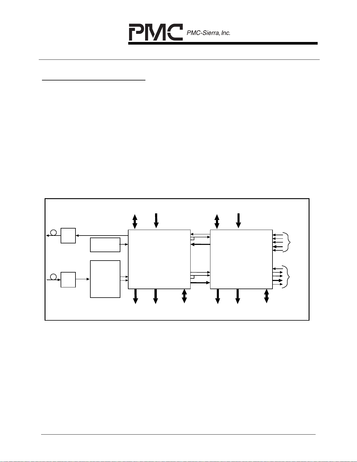
APPLICATION EXAMPLE
The STXC is typically used to implement a portion of an STS-3/STM-1 line
Interface. The STXC may find application in many different types of SONET/SDH
network elements including switches, terminal multiplexers, and add-drop
multiplexers. In such applications, the STXC typically interfaces on its line side
with a clock and data recovery device (for the receiver) and a physical media
device such as a laser (for the transmitter). The system side interfaces directly to
the PM5344 SONET/SDH Path Terminating Transceiver (SPTX) where pointer
processing and path overhead termination are performed for an STS-3/STM-1
stream. The initial configuration and ongoing control and monitoring of the STXC
are normally provided via a generic microprocessor interface.
Figure 1 - STS-3/STM-1 Line Interface
E/O
O/E
RSD+/-
Clock
Generation
Clock/Data
Recovery
TRANSMIT
TRANSPORT
OVERHEAD
ACCESS
TXD+/-
TXCI+/-
TRANSMIT
ALARM INSERT
SIGNALS
PM5343 STXC
155 Mbit/s
Transport Overhead
Transceiver
RXC+/RXD+/-
TIFP
TICLK
GTICLK
TIN[7:0]
ROFP
RICLK
GRICLK
ROUT[7:0]
TRANSMIT
PATH
OVERHEAD
ACCESS
FPOUT
TCK
TD[7:0]
IFP
PICLK
RD[7:0]
TRANSMIT
ALARM INSERT
SIGNALS
PM5344 SPTX
Path
Terminating
Transceiver
AC1J1V1
AD[7:0]
ADP
DCK
DC1J1V1
DD[7:0]
DDP
ACK
APL
DPL
Telecombus
Add
Interface
Telecombus
Drop
Interface
RECEIVE
TRANSPORT
OVERHEAD
ACCESS
RECEIVE
ALARM DETECT
SIGNALS
MICRO BUS
FOR CONFIG,
STATUS
AND CONTROL
RECEIVE
PATH
OVERHEAD
ACCESS
RECEIVE
ALARM DETECT
SIGNALS
MICRO BUS
FOR CONFIG,
STATUS
AND CONTROL
PROPRIETARY AND CONFIDENTIAL TO PMC-SIERRA INC., AND FOR ITS CUSTOMERS’ INTERNAL USE
5
Page 20
PM5343 STXC
DATA SHEET
PMC-930303 ISSUE 6 SONET/SDH TRANSPORT OVERHEAD TRANSCEIVER
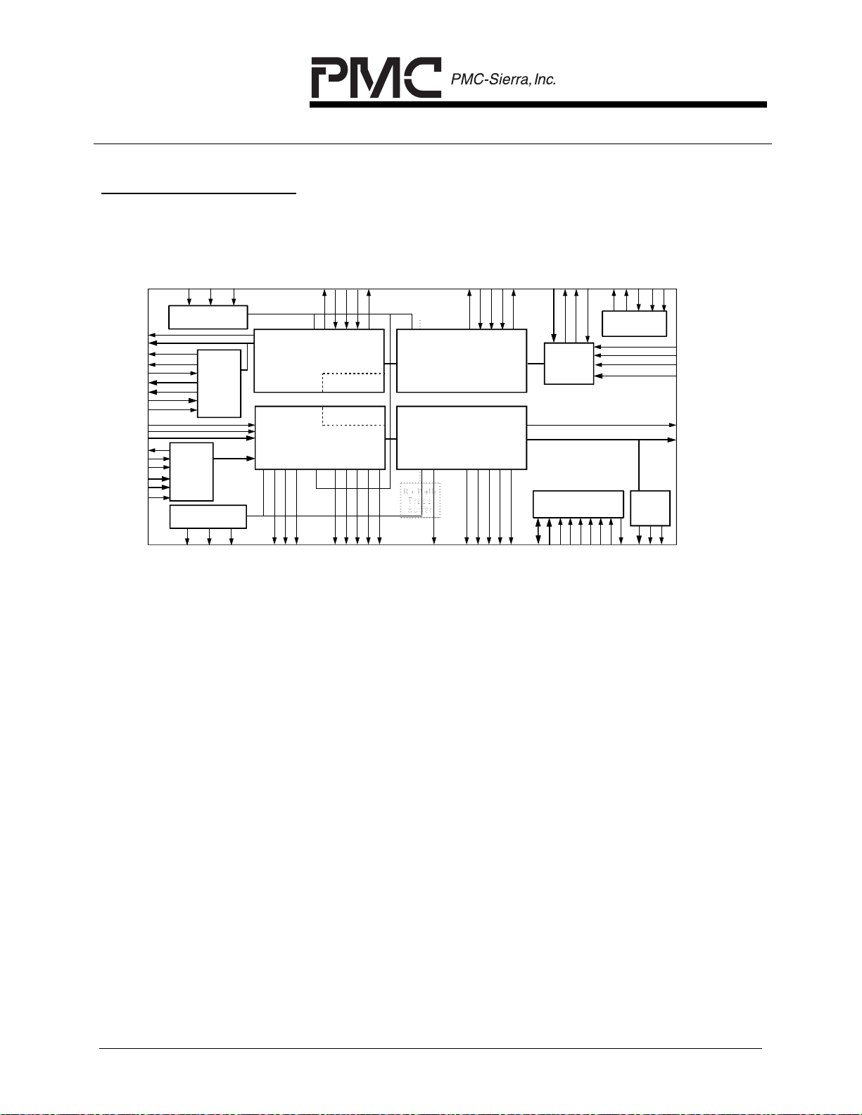
5
TOFP
TOUT[7:0]
GTICLK
TSOUT
TSICLK
TXD+/-
TXCO +/-
TXCI+/-
TSER
RICLK
RIFP
RIN[7:0]
GRICLK
RSIN
RSICLK
RXC+/-
RXD+/-
RSER
BLOCK DIAGRAM
CPDAT
TLAIS/TR
Transmit Ring
Co n trol Po rt
Serial
to
Parallel
Receive Ring
Control Port
LOS/RRCPFP
TRD I/TRCPFP
Parallel
to
Serial
LAIS/RRCPDAT
RLAIS/TRCPCLK
Tx Section O/H Processor
Rx Section O/H Processor
LOF
RDI/RRCPCLK
OOF
B1E
TSDCLK
TSD
Tx Section
Trace Buffer
Rx Section
Trace Buffer
RSD
RSDCLK
W
TSO
P
SCP O[5]/RDP
SCP O [4:0]
SCP I[1:0]
Status and
Rx
O/H
Access
INTB
RSTB
RTOH
PL
SCP I[3]/TD
SCP I[2]/T
RTOHFP
RTOHCLK
TDIS
TIFP/TC1J1V1
TICLK
TIN[7:0]
ROFP
ROUT[7:0]
K
W
TLD
TLO
TAPSCLK
TAPS
TTOHCLK
TTOHEN
TTOHFP
TTOH
TOWCL
TSUC
TLDCLK
Co n tro l Po rt
Tx
Tx Line O/H Processor
O/H
Access
APS
Rx Line O/H Processor
Rx Path
Trace
Buffer
RSUC
RSOW
ROW CLK
B2E
RLD
RLDCLK
RAPS
RLOW
RAPSCLK
Microprocessor
ALE
A[6:0]
D[7:0]
MBEB
I/F
CSB
RWB
RDB_E
WRB_
PROPRIETARY AND CONFIDENTIAL TO PMC-SIERRA INC., AND FOR ITS CUSTOMERS’ INTERNAL USE
6
Page 21

PM5343 STXC
DATA SHEET
PMC-930303 ISSUE 6 SONET/SDH TRANSPORT OVERHEAD TRANSCEIVER
6
DESCRIPTION
The PM5343 SONET/SDH 155 Mbit/s Transport Overhead Terminating
Transceiver (STXC) processes the transport overhead (section overhead) of
STS-1, and STS-3 (STM-1) streams at 51.84 Mbit/s and 155.52 Mbit/s. The
STXC implements significant functions for a SONET/SDH compliant line
interface.
The STXC receives SONET/SDH frames via a bit serial or byte serial interface
and processes section (regenerator section) and line (multiplexer section)
overhead. It performs framing (A1, A2), descrambling, detects alarm conditions,
and monitors section and line path bit interleaved parity (B1, B2), accumulating
error counts at each level for performance monitoring purposes. B2 errors are
also monitored to detect signal fail and signal degrade threshold crossing alarms.
Line remote error indications (M1) are also accumulated. A 16 or 64 byte section
trace (J0) message may be buffered and compared against an expected
message.
The STXC also provides convenient access to all transport overhead bytes,
which are extracted and serialized on lower rate interfaces, allowing additional
external processing of overhead.
The STXC transmits SONET/SDH frames, via a bit serial or a byte serial
interface, and formats section and line overhead appropriately. It performs
framing pattern insertion (A1, A2), scrambling, alarm signal insertion, and
creates section and line bit interleaved parity (B1, B2) as required to allow
performance monitoring at the far end. Line remote error indications (M1) are
optionally inserted. A 16 or 64 byte section trace (J0) message may be inserted.
The STXC also provides convenient access to all transport overhead bytes,
which are optionally inserted from lower rate serial interfaces, allowing external
sourcing of overhead. The STXC also supports the insertion of a large variety of
errors into the transmit stream, such as framing pattern errors and bit interleaved
parity errors, which are useful for system diagnostics and tester applications.
Ring control ports provide the ability to pass control and status information
between mate transceivers.
The transmitter and receiver are independently configurable to allow for
asymmetric interfaces. The STXC is configured, controlled and monitored via a
generic 8-bit microprocessor bus interface.
PROPRIETARY AND CONFIDENTIAL TO PMC-SIERRA INC., AND FOR ITS CUSTOMERS’ INTERNAL USE
7
Page 22

PM5343 STXC
DATA SHEET
PMC-930303 ISSUE 6 SONET/SDH TRANSPORT OVERHEAD TRANSCEIVER
The STXC is implemented in low power, +5 Volt, CMOS technology. It has TTL
and pseudo ECL (PECL) compatible inputs and outputs and is packaged in a
160 pin MQFP package.
PROPRIETARY AND CONFIDENTIAL TO PMC-SIERRA INC., AND FOR ITS CUSTOMERS’ INTERNAL USE
8
Page 23
PM5343 STXC
DATA SHEET
PMC-930303 ISSUE 6 SONET/SDH TRANSPORT OVERHEAD TRANSCEIVER
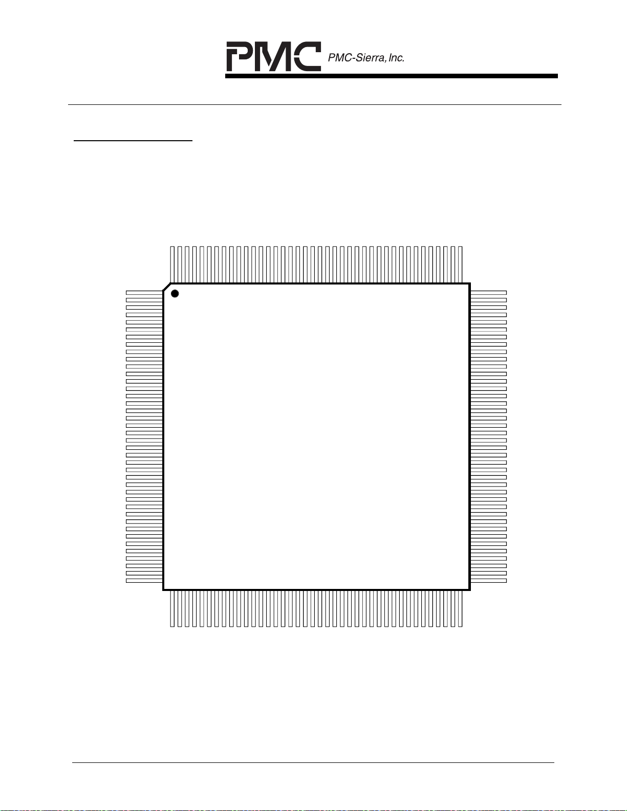
7
PIN DIAGRAM
The STXC is available in a 160 pin MQFP package having a body size of 28 mm
by 28 mm and a pin pitch of 0.65 mm.
PIN 1
TLDCLK
TLD
TOWCLK
TSUC
TSOW
TSDCLK
RLAIS/TRCPCLK
TLAIS/TRCPDAT
TSD
TRDI/TRCPFP
TSICLK
TSER
VT1
TAVD1
TXCO-
TXCO+
TAVS1
TAVD2
TAVS2
TAVD3
TAVS3
TXD+
TXD-
TAVS4
VT2
TAVD4
TXCI-
TXCI+
TSOUT
TOUT[0]
TOUT[1]
TOUT[2]
TOUT[3]
VSSO
VDDO
TOUT[4]
TOUT[5]
TOUT[6]
TOUT[7]
TOFP
PIN 160
W
TLO
VSSO
TAPS
TAPSCLK
Index
J1V1
VDDO
VSSO
VSSO
ROUT[0]
ROUT[1]
RICLK
VDDO
GRICLK
ROFP
TIN[6]
TIN[3]
TIN[4]
TTOHCLK
TTOHEN
TDIS
TTOHFP
TTOH
VDDO
TIN[0]
TIN[5]
TIN[1]
TIN[2]
TIN[7]
TIFP/TC1
VSSI
GTICLK
TICLK
VDDI
ROUT[4]
ROUT[5]
ROUT[6]
ROUT[7]
MBEB
ROUT[2]
ROUT[3]
ALE
PIN 121
PIN 120
A[0]
A[1]
A[2]
A[3]
A[4]
A[5]
A[6]
RDB_E
WRB_RWB
CSB
RSTB
D[0]
D[1]
D[2]
D[3]
PM 5343
STXC
Top
View
D[4]
D[5]
VDDO
VSSO
D[6]
D[7]
INTB
SCPO[0]
SCPO[1]
SCPO[2]
SCPO[3]
SCPO[4]
SCPO[5]/RDP
SCPI[0]
SCPI[1]
SCPI[2]/TPL
SCPI[3]/TDP
RTOHCLK
RTOH
VDDO
VSSO
RTOHFP
RAPSCLK
RAPS
RLOW
PIN 40
VDDI
VSSO
B2E
RLD
RLDCLK
9
PIN 41 PIN 80
RIFP
VDDI
RIN[2]
RIN[3]
RIN[0]
RIN[1]
VSSI
RIN[4]
RIN[5]
RIN[6]
B1E
LOF
OOF
RSIN
RSER
RIN[7]
RSICLK
CRX
C+
RX
DRX
RAVS
RAVD
D+
RX
VDDO
VSSO
RSD
RSUC
RSOW
RSDCLK
ROWCLK
VSSI
VDDO
LOS/RRCPFP
RDI/RRCPCLK
LAIS/RRCPDAT
PROPRIETARY AND CONFIDENTIAL TO PMC-SIERRA INC., AND FOR ITS CUSTOMERS’ INTERNAL USE
PIN 81
Page 24

PM5343 STXC
DATA SHEET
PMC-930303 ISSUE 6 SONET/SDH TRANSPORT OVERHEAD TRANSCEIVER
8
PIN DESCRIPTION
Pin Name Pin Ty pe Pin
Function
No.
RSER Input 52 The receive serial input (RSER) selects the
receive line interface. RSER is tied high to
select the bit serial interface on PECL pins
RXC+, RXC-, RXD+, and RXD-. A TTL
interface is also supported in STS-1 mode on
pins RSIN and RSICLK. RSER is tied low to
select the byte serial interface (on pins RICLK,
RIN[7:0], and RIFP).
RICLK/ Input 135 The receive incoming clock (RICLK) provides
timing for processing the byte serial receive
stream, RIN[7:0]. RICLK is nominally a 6.48
MHz (STS-1), or 19.44 MHz (STS-3/S TM-1)
50% duty cycle clock, depending on the
selected operating mode. RIN[7:0], and RIFP
are sampled on the rising edge of RICLK.
RICLK must be externally shorted directly to
GRICLK when processing a bit serial receive
stream.
RVCLK The receive vector clock (RVCLK) is used
during STXC production test to verify internal
functionality.
RIN[7]
RIN[6]
RIN[5]
RIN[4]
Input
Input
Input
Input
51
49
48
47
The receive incoming stream (RIN[7:0]) carries
the scrambled STS-1 or STS-3/STM-1 stream
in byte serial format. RIN[7] is the most
significant bit (corresponding to bit 1 of each
serial PCM word, the first bit transmitted).
RIN[0] is the least significant bit (corresponding
RIN[3]
RIN[2]
Input
Input
46
44
to bit 8 of each serial PCM word, the last bit
transmitted). RIN[7:0] is sampled on the rising
edge of RICLK.
RIN[1]
RIN[0]
Input
Input
43
42
PROPRIETARY AND CONFIDENTIAL TO PMC-SIERRA INC., AND FOR ITS CUSTOMERS’ INTERNAL USE
10
Page 25

PM5343 STXC
DATA SHEET
PMC-930303 ISSUE 6 SONET/SDH TRANSPORT OVERHEAD TRANSCEIVER
Pin Name Pin Ty pe Pin
Function
No.
RIFP Input 41 The active high receive incoming framing
position (RIFP) signal indicates when the first
byte of the synchronous payload envelope is
available on the RIN[7:0] inputs. RIFP is
sampled on the rising edge of RICLK.
RSIN Input 53 The receive incoming serial stream (RSIN)
contains the TTL compatible 51.84 Mbit/s
receive STS-1 stream. RSIN is sampled on the
rising edge of RSICLK. The RSIN input has an
integral pull down resistor. The RXD+/- inputs
may also carry the receive STS-1 stream.
RSICLK Input 54 The receive serial incoming clock (RSICLK)
provides timing for processing the bit serial
receive stream, RSIN when the TTL bit serial
STS-1 mode is selected. RSICLK is nominally
a 51.84 MHz, 50% duty cycle clock. RSIN is
sampled on the rising edge of RSICLK.
RSICLK is divided by eight to produce GRICLK
when the TTL bit serial STS-1 mode is
selected. The RSICLK input has an integral
pull down resistor.
RXD+
RXD-
PECL
Input
63
62
The receive differential data inputs (RXD+,
RXD-) contain the 155.52 Mbit/s receive STS-
3/STM-1 or 51.84 Mbit/s receive STS-1 stream.
RXD+/- is sampled on the rising edge of
RXC+/- (the falling edge may be used by
reversing RXC+/-).
RXC+
RXC-
PECL
Input
59
58
The receive differential clock inputs (RXC+,
RXC-) provides timing for processing the bit
serial receive stream, RXD+/- when the PECL
bit serial mode is selected. RXC+/- is
nominally a 155.52 MHz or 51.84 MHz, 50%
duty cycle clock. RXD+/- is sampled on the
rising edge of RXC+/-. RXC+/- is divided by
eight to produce GRICLK when the PECL bit
serial mode is selected.
PROPRIETARY AND CONFIDENTIAL TO PMC-SIERRA INC., AND FOR ITS CUSTOMERS’ INTERNAL USE
11
Page 26

PM5343 STXC
DATA SHEET
PMC-930303 ISSUE 6 SONET/SDH TRANSPORT OVERHEAD TRANSCEIVER
Pin Name Pin Ty pe Pin
Function
No.
RLAIS/ Input 8 The receive line AIS insertion (RLAIS) signal
controls the insertion of line AIS in the receive
outgoing stream, ROUT[7:0], when the ring
control port is disabled. When RLAIS is high,
line AIS is inserted in the outgoing stream.
Line AIS is also optionally inserted
automatically upon detection of loss of signal,
loss of frame, section trace alarms or line AIS
in the incoming stream. RLAIS is sampled on
the rising edge of RICLK.
TRCPCLK The transmit ring control port clock (TRCPCLK)
signal provides timing for the transmit ring
control port when the ring control port is
enabled (the enabling and disabling of the ring
control port is controlled by a bit in the Master
Control Register). TRCPCLK is nominally a
3.24 MHz, 50% duty cycle clock and is
normally connected to the RRCPCLK output of
a mate STXC in ring-based add-drop
multiplexer applications. TRCPFP and
TRCPDAT are sampled on the rising edge of
TRCPCLK.
OOF Output 57 The out of frame (OOF) signal is set high while
the STXC is unable to find a valid framing
pattern (A1, A2) in the incoming stream. OOF
is set low when a valid framing pattern is
detected. OOF is updated on the rising edge
of RICLK.
LOF Output 56 The loss of frame (LOF) signal is set high when
an out of frame state persists for 3 ms. LOF is
set low when an in frame state persists for 3
ms. LOF is updated on the rising edge of
RICLK.
PROPRIETARY AND CONFIDENTIAL TO PMC-SIERRA INC., AND FOR ITS CUSTOMERS’ INTERNAL USE
12
Page 27

PM5343 STXC
DATA SHEET
PMC-930303 ISSUE 6 SONET/SDH TRANSPORT OVERHEAD TRANSCEIVER
Pin Name Pin Ty pe Pin
Function
No.
LOS/ Output 71 Loss of signal (LOS) is active when the ring
control port is disabled. Loss of signal (LOS) is
set high when a violating period (20 ± 2.5 µs)
of consecutive all zeros patterns is detected in
the incoming stream. LOS is set low when two
valid framing words (A1, A2) are detected, and
during the intervening time (125 µs), no
violating period of all zeros patterns is
observed. LOS is updated on the r ising edge
of RICLK.
RRCPFP The receive ring control port frame position
(RRCPFP) signal identifies bit positions in the
receive ring control port data (RRCPDAT) when
the ring control port is enabled (the enabling
and disabling of the ring control port is
controlled by a bit in the Master Control
Register). RRCPFP is high during the filtered
K1, K2 bit positions, the change of APS value
bit position, the protection switch byte failure bit
position, and the send AIS and send RDI bit
positions in the RRCPDAT stream. RRCPFP is
normally connected to the TRCPFP input of a
mate STXC in ring-based add-drop multiplexer
applications. RRCPFP is updated on the falling
edge of RRCPCLK.
B1E Output 55 The B1 error clock (B1E) is a return to zero
signal that pulses high for 154 ns with a
minimum low time of 154 ns for every section
bit interleaved parity error (B1) detected in the
incoming stream. Up to eight pulses may occur
on B1E per frame.
PROPRIETARY AND CONFIDENTIAL TO PMC-SIERRA INC., AND FOR ITS CUSTOMERS’ INTERNAL USE
13
Page 28

PM5343 STXC
DATA SHEET
PMC-930303 ISSUE 6 SONET/SDH TRANSPORT OVERHEAD TRANSCEIVER
Pin Name Pin Ty pe Pin
Function
No.
RDI/ Output 73 The far end receive failure (RDI) signal is active
when the ring control port is disabled. RDI is
set high when line RDI is detected in the
incoming stream. RDI is declared when a 110
binary pattern is detected in bits 6, 7, and 8 of
the K2 byte for three or five consecutive
frames. RDI is removed when any pattern
other than 110 is detected in bits 6, 7, and 8 of
the K2 byte for three or five consecutive
frames. This alarm indication is also available
through register access. RDI is updated on the
rising edge of RICLK.
RRCPCLK The receive ring control port clock (RRCPCLK)
signal provides timing for the receive ring
control port when the ring control port is
enabled (the enabling and disabling of the ring
control port is controlled by a bit in the Master
Control Register). RRCPCLK is nominally a
3.24 MHz, 50% duty cycle clock and is
normally connected to the TRCPCLK input of a
mate STXC in ring-based add-drop multiplexer
applications. RRCPFP and RRCPDAT are
updated on the falling edge of RRCPCLK.
PROPRIETARY AND CONFIDENTIAL TO PMC-SIERRA INC., AND FOR ITS CUSTOMERS’ INTERNAL USE
14
Page 29

PM5343 STXC
DATA SHEET
PMC-930303 ISSUE 6 SONET/SDH TRANSPORT OVERHEAD TRANSCEIVER
Pin Name Pin Ty pe Pin
Function
No.
LAIS/ Output 72 The line alarm indication (LAIS) signal is active
when the ring control port is disabled. LAIS is
set high when line AIS is detected in the
incoming stream. LAIS is declared when a 111
binary pattern is detected in bits 6, 7, and 8 of
the K2 byte for three or five consecutive
frames. LAIS is removed when any pattern
other than 111 is detected in bits 6, 7, and 8 of
the K2 byte for three or five consecutive
frames. This alarm indication is also available
through register access. LAIS is updated on
the rising edge of RICLK.
RRCPDAT The receive ring control port data (RRCPDAT)
signal contains the receive ring control port
data stream when the ring control port is
enabled (the enabling and disabling of the ring
control port is controlled by a bit in the Master
Control Register). The receive ring control port
data consists of the filtered K1, K2 byte values,
the change of APS value bit position, the
protection switch byte failure status bit position,
the send AIS and send RDI bit positions, and
the line REI bit positions. RRCPDAT is
normally connected to the TRCPDAT input of a
mate STXC in ring-based add-drop multiplexer
applications. RRCPDAT is updated on the
falling edge of RRCPCLK.
B2E Output 78 The B2 error clock (B2E) is a return to zero
signal that pulses 154 ns with a minimum low
time of 154 ns for every line bit interleaved
parity error (B2) detected in the incoming
stream. Up to 8 (STS-1), or 24 (STS-3/S TM-1)
pulses may occur on B2E, per frame.
RSDCLK Output 67 The receive section DCC clock (RSDCLK) is a
192 kHz clock used to update the RSD output.
RSDCLK is generated by gapping a 216 kHz
clock.
PROPRIETARY AND CONFIDENTIAL TO PMC-SIERRA INC., AND FOR ITS CUSTOMERS’ INTERNAL USE
15
Page 30

PM5343 STXC
DATA SHEET
PMC-930303 ISSUE 6 SONET/SDH TRANSPORT OVERHEAD TRANSCEIVER
Pin Name Pin Ty pe Pin
Function
No.
RSD Output 66 The receive section DCC (RSD) signal contains
the section data communications channel (D1,
D2, D3) extracted from the incoming stream.
RSD is updated on the falling edge of
RSDCLK.
ROWCLK Output 70 The receive order wire clock (ROWCLK) is a 64
kHz clock used to update the RSOW, RSUC,
and RLOW outputs. ROWCLK is generated by
gapping a 72 kHz clock.
RSOW Output 68 The receive section order wire (RSOW) signal
contains the section order wire channel (E1)
extracted from the incoming stream. RSOW is
updated on the falling edge of ROWCLK.
RSUC Output 69 The receive section user channel (RSUC)
signal contains the section user channel (F1)
extracted from the incoming stream. RSUC is
updated on the falling edge of ROWCLK.
RLOW Output 81 The receive line order wire (RLOW) signal
contains the line order wire channel (E2)
extracted from the incoming stream. RLOW is
updated on the falling edge of ROWCLK.
RLDCLK Output 80 The receive line DCC clock (RLDCLK) is a 576
kHz clock used to update the RLD output.
RLDCLK is generated by gapping a 2.16 MHz
clock.
RLD Output 79 The receive line DCC (RLD) signal contains the
line data communications channel (D4 - D12)
extracted from the incoming stream. RLD is
updated on the falling edge of RLDCLK.
RAPSCLK Output 83 The receive automatic protection switch
channel clock (RAPSCLK) is a 128 kHz clock
used to update the RAPS output. RAPSCLK is
generated by gapping a 144 kHz clock.
PROPRIETARY AND CONFIDENTIAL TO PMC-SIERRA INC., AND FOR ITS CUSTOMERS’ INTERNAL USE
16
Page 31

PM5343 STXC
DATA SHEET
PMC-930303 ISSUE 6 SONET/SDH TRANSPORT OVERHEAD TRANSCEIVER
Pin Name Pin Ty pe Pin
Function
No.
RAPS Output 82 The receive automatic protection switch
channel (RAPS) signal carries the automatic
protection switch channel (K1, K2) extracted
from the incoming stream. RAPS is updated
on the falling edge of RAPSCLK.
RTOH Output 87 The receive transport overhead (RTOH) signal
contains the receive transport overhead bytes
(A1, A2, J0, Z0, B1, E1, F1, D1-D3, H1-H3, B2,
K1, K2, D4-D12, Z1, Z2, and E2) extracted
from the incoming stream. RTOH is updated
on the falling edge of RTOHCLK.
RTOHCLK Output 88 The receive transport overhead clock
(RTOHCLK) is nominally a 5.184 MHz or 1.728
MHz clock that provides timing to process the
extracted receive transport overhead, RTOH.
RTOHCLK is a gapped 6.48 MHz clock when
accessing the transport overhead of an STS-
3/STM-1 stream. RTOHCLK is a gapped 2.16
MHz clock when accessing the transport
overhead of an STS-1 stream.
RTOHFP Output 84 The receive transport overhead frame position
(RTOHFP) signal is used to locate the
individual receive transport overhead bits in the
receive transport overhead, RTOH. RTOHFP is
set high while bit 1 (the most significant bit) of
the first framing byte (A1) is present in the
RTOH stream. RTOHFP is updated on the
falling edge of RTOHCLK.
PROPRIETARY AND CONFIDENTIAL TO PMC-SIERRA INC., AND FOR ITS CUSTOMERS’ INTERNAL USE
17
Page 32

PM5343 STXC
DATA SHEET
PMC-930303 ISSUE 6 SONET/SDH TRANSPORT OVERHEAD TRANSCEIVER
Pin Name Pin Ty pe Pin
Function
No.
GRICLK Output 134 When either of the bit serial receive interfaces
are enabled, GRICLK is the generated byte
serial clock. When the bit serial STS-1 mode is
enabled, GRICLK is a 6.48 MHz clock that is
generated by dividing the receive serial
incoming clock (RSICLK) by eight. When the
bit serial STS-3 mode is enabled, GRICLK is a
19.44 MHz clock that is generated by dividing
the receive serial incoming clock (RSC+/-) by
eight. GRICLK must be externally shorted
directly to the receive incoming clock (RICLK)
when processing a bit serial stream.
ROUT[7]
ROUT[6]
ROUT[5]
ROUT[4]
Output
Output
Output
Output
123
124
125
126
ROUT[7:0] contains the descrambled outgoing
stream in byte serial format. ROUT[7] is the
most significant bit (corresponding to bit 1 of
each serial PCM word, the first bit received).
ROUT[0] is the least significant bit
(corresponding to bit 8 of each serial PCM
ROUT[3]
ROUT[2]
Output
Output
127
128
word). ROUT[7:0] is updated on the rising
edge of RICLK.
ROUT[1]
ROUT[0]
Output
Output
131
132
ROFP Output 133 The active high receive outgoing frame position
(ROFP) signal is set high once per frame in the
byte position immediately following the Z0
bytes in the ROUT[7:0] stream. ROFP is also
used to mark the alignment of the RSOW,
RSUC, RLOW and RAPS bit streams.
ROFP is updated on the rising edge of RICLK.
TSER Input 12 The transmit serial input (TSER) selects the
transmit line interface. TSER is tied high to
select the bit serial interface on PECL pins
TXCI+, TXCI-, TXCO+, TXCO-, TXD+, and
TXD-. A TTL interface is also supported in
STS-1 mode on pins TSICLK and TSOUT.
TSER is tied low to select the byte serial
interface on pins TICLK, TOFP, and TOUT[7:0].
PROPRIETARY AND CONFIDENTIAL TO PMC-SIERRA INC., AND FOR ITS CUSTOMERS’ INTERNAL USE
18
Page 33

PM5343 STXC
DATA SHEET
PMC-930303 ISSUE 6 SONET/SDH TRANSPORT OVERHEAD TRANSCEIVER
Pin Name Pin Ty pe Pin
Function
No.
TICLK/ Input 140 The transmit incoming clock (TICLK) provides
timing for processing the transmit stream,
TIN[7:0]. TICLK is nominally a 6.48 MHz (STS-
1), or 19.44 MHz (STS-3/STM-1) 50% duty
cycle clock, depending on the selected
operating mode. TIN[7:0], and TIFP are
sampled on the rising edge of TICLK. TICLK
must be externally shorted directly to GTICLK
when processing bit serial transmit streams.
TVCLK The transmit vector clock (TVCLK) is used
during STXC production test to verify internal
functionality.
GTICLK Output 141 When either of the bit serial transmit interfaces
are enabled, GTICLK is the generated byte
serial clock. GTICLK is a 6.48 MHz or 19.44
MHz clock that is generated by dividing the
transmit serial incoming clock (TSICLK or
TXCI+/-) by eight. GTICLK must be externally
shorted directly to the transmit incoming clock
(TICLK) when processing a bit serial stream.
In line loopback mode operation (LLE bit set
high), GTICLK is generated by dividing the
RXC+/- inputs by eight.
TSICLK Input 11 The transmit serial incoming clock (TSICLK)
provides timing for updating the bit serial
outgoing stream when STS-1 mode is selected.
TSICLK is nominally a 51.84 MHz, 50% duty
cycle clock. TSOUT is updated on the rising
edge of TSICLK. The TSICLK input has an
integral pull down resistor. The device may be
configured to use the TXCI+/- inputs as the
serial clock.
TXCI+
TXCI-
PECL
Input
28
27
The transmit differential clock inputs (TXCI+,
TXCI-) provide timing for updating the bit serial
outgoing stream. TXCI+/- is nominally a 155.52
MHz or 51.84 MHz, 50% duty cycle clock. The
TSICLK is the default clock for the 51.84 Mbit/s
data rate.
PROPRIETARY AND CONFIDENTIAL TO PMC-SIERRA INC., AND FOR ITS CUSTOMERS’ INTERNAL USE
19
Page 34

PM5343 STXC
DATA SHEET
PMC-930303 ISSUE 6 SONET/SDH TRANSPORT OVERHEAD TRANSCEIVER
Pin Name Pin Ty pe Pin
Function
No.
TIN[7]
TIN[6]
TIN[5]
TIN[4]
Input 143
144
145
146
The transmit incoming bus, (TIN[7:0]), carries
an STS-1 or STS-3/STM-1 stream in byte serial
format. TIN[7] is the most significant bit
(corresponding to bit 1 of each serial PCM
word, the first bit transmitted). TIN[0] is the
least significant bit (corresponding to bit 8 of
TIN[3]
TIN[2]
TIN[1]
TIN[0]
147
148
149
150
each serial PCM word). TIN[7:0] is sampled on
the rising edge of TICLK.
TIFP/ Input 142 The active high transmit incoming framing
position (TIFP/TC1J1V1) signal indicates the
frame alignment for incoming streams. When
Register Mode Select bit C1EN is logic 0, a
high level on TIFP marks the byte immediately
following the Z0 bytes in the transmit STS-1 or
STS-3 (STM-1) stream, TIN[7:0].
TC1J1V1 When Register Mode Select bit C1EN is logic
1, a high level on TIFP marks the first J0 byte
in the transmit STS-1 or STS-3 (STM-1)
stream, TIN[7:0]. TIFP/TC1J1V1 is sampled on
the rising edge of TICLK.
PROPRIETARY AND CONFIDENTIAL TO PMC-SIERRA INC., AND FOR ITS CUSTOMERS’ INTERNAL USE
20
Page 35

PM5343 STXC
DATA SHEET
PMC-930303 ISSUE 6 SONET/SDH TRANSPORT OVERHEAD TRANSCEIVER
Pin Name Pin Ty pe Pin
Function
No.
TDIS Input 151 The active high transmit disable (TDIS) signal
selectively disables overwriting the STS-1 or
STS-3 (STM-1) byte serial stream with the
corresponding overhead byte. TDIS is sampled
on the rising edge of TICLK. TDIS takes
precedence over the TTOHEN and TTOH
inputs.
In general, the value on TIN[7:0] passes
through transparently if TDIS is high. Three
exceptions exist:
1.) Bits 6 to 8 of the K2 byte may be overwritten
by a active RDI indication ("110") regardless of
the state of TDIS.
2.) If TDIS is high during the section BIP byte
(B1), the TIN[7:0] value becomes an error
mask for the generated section BIP.
3.) If TDIS is high during the line BIP bytes
(B2), and the DB2 bit in the TLOP Control
register is logic 0, the TIN[7:0] value becomes
an error mask for the generated line BIP.
TTOH Input 155 The transmit transport overhead bus (TTOH)
contains the transport overhead bytes (A1, A2,
J0, Z0, E1, F1, D1-D3, H3, K1, K2, D4-D12,
Z1, Z2, and E2) and error masks (H1, H2, B1,
and B2) which may be inserted, or used to
insert bit interleaved parity errors or payload
pointer bit errors into the overhead byte
positions in the outgoing stream. Insertion is
controlled by the TTOHEN input. TTOH is
sampled on the rising edge of TTOHCLK.
PROPRIETARY AND CONFIDENTIAL TO PMC-SIERRA INC., AND FOR ITS CUSTOMERS’ INTERNAL USE
21
Page 36

PM5343 STXC
DATA SHEET
PMC-930303 ISSUE 6 SONET/SDH TRANSPORT OVERHEAD TRANSCEIVER
Pin Name Pin Ty pe Pin
Function
No.
TTOHFP Output 156 The transmit transport overhead frame position
(TTOHFP) signal is used to locate the
individual transport overhead bits in the
transport overhead bus, TTOH. TTOHFP is set
high while bit 1 (the most significant bit) of the
first framing byte (A1) is expected in the
incoming stream. TTOHFP is updated on the
falling edge of TTOHCLK.
TTOHCLK Output 153 The transmit transport overhead clock
(TTOHCLK) is nominally a 5.184 MHz (1.728
MHz for STS-1) clock that provides timing for
upstream circuitry that sources the transport
overhead, TTOH. TTOHCLK is a gapped 6.48
MHz clock when accessing the transport
overhead of STS-3/STM-1 streams. TTOHCLK
is a gapped 2.16 MHz clock when accessing
the transport overhead of an STS-1 stream.
PROPRIETARY AND CONFIDENTIAL TO PMC-SIERRA INC., AND FOR ITS CUSTOMERS’ INTERNAL USE
22
Page 37

PM5343 STXC
DATA SHEET
PMC-930303 ISSUE 6 SONET/SDH TRANSPORT OVERHEAD TRANSCEIVER
Pin Name Pin Ty pe Pin
Function
No.
TTOHEN Input 152 The transmit transport overhead insert enable
(TTOHEN) signal controls the source of the
transport overhead data which is inserted in
the transmit stream. While TTOHEN is high
during the most significant bit of a TTOH byte
(and TDIS is low), values sampled on the TTOH
input are inserted into the corresponding
transport overhead bit positions (for the A1, A2,
J0, Z0, E1, F1, D1-D3, H3, K1, K2, D4-D12,
Z1, Z2, and E2 bytes). While TTOHEN is low
during the most significant bit of a TTOH byte,
the default values are inserted into these
transport overhead byte positions. A high level
on TTOHEN during most significant bit of TTOH
for the H1, H2, B1, or B2 bytes enables an
error mask. While the error mask is enabled, a
high level on TTOH causes the corresponding
H1, H2, B1 or B2 bit positions to be inverted.
When the section trace enable (STEN) bit is a
logic 1, the J0 byte contents are sourced from
the section trace buffer, regardless of the state
of TTOHEN. A low level on TTOH allows the
corresponding bit positions to pass through the
STXC uncorrupted. TTOHEN is sampled on
the rising edge of TTOHCLK.
PROPRIETARY AND CONFIDENTIAL TO PMC-SIERRA INC., AND FOR ITS CUSTOMERS’ INTERNAL USE
23
Page 38

PM5343 STXC
DATA SHEET
PMC-930303 ISSUE 6 SONET/SDH TRANSPORT OVERHEAD TRANSCEIVER
Pin Name Pin Ty pe Pin
Function
No.
TRDI/ Input 10 The active high transmit far end receive failure
(TRDI) signal controls the insertion of a far end
receive failure indication in the outgoing stream
when the ring control port is disabled. When
TRDI is set high, bits 6, 7, and 8 of the K2 byte
are set to the pattern 110. Line RDI may also
be inserted using the RDI bit in the TLOP
Control Register, or upon detection of loss of
signal, loss of frame, or line AIS in the receive
stream, using the AUTORDI bit in the Master
Control/Enable Register. The TRDI input takes
precedence over the TTOH and TTOHEN
inputs. TRDI is sampled on the rising edge of
TICLK.
TRCPFP The transmit ring control port frame position
(TRCPFP) signal identifies bit positions in the
transmit ring control port data (TRCPDAT)
when the ring control port is enabled (the
enabling and disabling of the ring control port is
controlled by a bit in the Master Control
Register). TRCPFP is high during the filtered
K1, K2 bit positions, the change of APS value
bit position, the protection switch byte failure bit
position, and the send AIS and send RDI bit
positions in the TRCPDAT stream. TRCPFP is
normally connected to the RRCPFP output of a
mate STXC in ring-based add-drop multiplexer
applications. TRCPFP is sampled on the rising
edge of TRCPCLK.
PROPRIETARY AND CONFIDENTIAL TO PMC-SIERRA INC., AND FOR ITS CUSTOMERS’ INTERNAL USE
24
Page 39

PM5343 STXC
DATA SHEET
PMC-930303 ISSUE 6 SONET/SDH TRANSPORT OVERHEAD TRANSCEIVER
Pin Name Pin Ty pe Pin
Function
No.
TLAIS/ Input 9 The active high transmit line alarm indication
signal (TLAIS) controls the insertion of line AIS
in the outgoing stream when the ring control
port is disabled. When TLAIS is set high, the
complete frame (except the section overhead
or regenerator section) is overwritten with the
all ones pattern (before scrambling). The
TLAIS input takes precedence over the TTOH
and TTOHEN inputs. TLAIS is sampled on the
rising edge of TICLK.
TRCPDAT The transmit ring control port data (TRCPDAT)
signal contains the transmit ring control port
data stream when the ring control port is
enabled (the enabling and disabling of the ring
control port is controlled by a bit in the Master
Control Register). The transmit ring control
port data consists of the filtered K1, K2 byte
values, the change of APS value bit position,
the protection switch byte failure status bit
position, the send AIS and send RDI bit
positions, and the line REI bit positions.
TRCPDAT is normally connected to the
RRCPDAT output of a mate STXC in ring-
based add-drop multiplexer applications.
TRCPDAT is sampled on the rising edge of
TRCPCLK.
TSDCLK Ou t put 6 The transmit section DCC clock (TSDCLK) is a
192 kHz clock used to sample the TSD input.
TSDCLK is generated by gapping a 216 kHz
clock.
TSD Input 7 The transmit section DCC (TSD) signal
contains the section data communications
channel (D1, D2, D3) inserted into the outgoing
stream. The TTOHEN input takes precedence
over TSD. TSD is sampled on the rising edge
of TSDCLK.
PROPRIETARY AND CONFIDENTIAL TO PMC-SIERRA INC., AND FOR ITS CUSTOMERS’ INTERNAL USE
25
Page 40

PM5343 STXC
DATA SHEET
PMC-930303 ISSUE 6 SONET/SDH TRANSPORT OVERHEAD TRANSCEIVER
Pin Name Pin Ty pe Pin
Function
No.
TOWCLK Output 3 The transmit order wire clock (TOWCLK) is a
64 kHz clock used to sample the TSOW, TSUC,
and TLOW inputs. TOWCLK is generated by
gapping a 72 kHz clock.
TSOW Input 5 The transmit section order wire (TSOW) signal
contains the section order wire channel (E1)
inserted into the outgoing stream. The
TTOHEN input takes precedence over TSOW.
TSOW is sampled on the rising edge of
TOWCLK.
TSUC Input 4 The transmit section user channel (TSUC)
signal contains the section user channel (F1)
inserted into the outgoing stream. The
TTOHEN input takes precedence over TSUC.
TSUC is sampled on the rising edge of
TOWCLK.
TLOW Input 160 The transmit line order wire (TLOW) signal
contains the line order wire channel (E2)
inserted into the outgoing stream. The
TTOHEN input takes precedence over TLOW.
TLOW is updated on the rising edge of
TOWCLK.
TLDCLK Output 1 The transmit line DCC clock (TLDCLK) is a 576
kHz clock used to sample the TLD input.
TLDCLK is generated by gapping a 2.16 MHz
clock.
TLD Input 2 The transmit line DCC (TLD) signal contains
the line data communications channel (D4 -
D12) inserted into the outgoing stream. The
TTOHEN input takes precedence over TLD.
TLD is sampled on the rising edge of TLDCLK.
TAPSCLK Output 157 The transmit automatic protection switch
channel clock (TAPSCLK) is a 128 kHz clock
used to sample the TAPS input. TAPSCLK is
generated by gapping a 144 kHz clock.
PROPRIETARY AND CONFIDENTIAL TO PMC-SIERRA INC., AND FOR ITS CUSTOMERS’ INTERNAL USE
26
Page 41

PM5343 STXC
DATA SHEET
PMC-930303 ISSUE 6 SONET/SDH TRANSPORT OVERHEAD TRANSCEIVER
Pin Name Pin Ty pe Pin
Function
No.
TAPS Input 158 The transmit automatic protection switch
channel (TAPS) signal carries the automatic
protection switch channel (K1, K2) inserted into
the outgoing stream. The TTOHEN input takes
precedence over TAPS. TAPS is sampled on
the rising edge of TAPSCLK.
TOUT[7]
TOUT[6]
TOUT[5]
TOUT[4]
Output
Output
Output
Output
39
38
37
36
The transmit outgoing stream, (TOUT[7:0]),
carries the scrambled STS-1, or STS-3/STM-1
stream. TOUT[7] is the most significant bit
(corresponding to bit 1 of each serial PCM
word, the first bit transmitted). TOUT[0] is the
least significant bit (corresponding to bit 8 of
TOUT[3]
TOUT[2]
TOUT[1]
TOUT[0]
Output
Output
Output
Output
33
32
31
30
each serial PCM word). TOUT[7:0] is updated
on the rising edge of TICLK.
TSOUT Output 29 The transmit serial outgoing stream, (TSOUT),
contains the scrambled stream in bit serial
format when serial STS-1 mode is selected.
TSOUT is updated on the rising edge of
TSICLK or TXCI+/-.
TXD+
TXD-
PECL
Output
22
23
The transmit differential data/positive pulse
outputs (TXD+, TXD-) contain the scrambled
stream in bit serial format when serial mode is
selected. TXD+/- is updated on the falling edge
of TXCO+/-.
TXCO+
TXCO-
PECL
Output
16
15
The transmit differential clock/negative pulse
outputs (TXCO+, and TXCO-) contain transmit
output clock. TXCO+/- is a buffered version of
TXCI+/-. TXD+/- is updated on the falling edge
of TXCO+/-.
PROPRIETARY AND CONFIDENTIAL TO PMC-SIERRA INC., AND FOR ITS CUSTOMERS’ INTERNAL USE
27
Page 42

PM5343 STXC
DATA SHEET
PMC-930303 ISSUE 6 SONET/SDH TRANSPORT OVERHEAD TRANSCEIVER
Pin Name Pin Ty pe Pin
Function
No.
TOFP Output 40 The active high transmit outgoing frame
position (TOFP) signal is asserted once per
frame in the byte position immediately following
the Z0 bytes in the TOUT[7:0] stream. TOFP is
also used to mark the alignment of the TSUC,
TSOW, TLOW, and TAPS bit streams. TOFP is
updated on the rising edge of TICLK.
SCPO[5] Output 93 The control output (SCPO[5]) is used to control
an auxiliary device when the RDPEN bit in the
Mode Select register is set to logic 0. The
signal level on this output corresponds to the
bit value contained in the Output Port register.
RDP The receive parity (RDP) signal indicates the
parity of the receive bus when the RDPEN bit
in the Mode Select register is set to logic 1.
The receive data bus (ROUT[7:0]]) is always
included in the parity calculation. Internal
register bits in the Mode Select register control
the inclusion of ROFP in the parity calculation,
and the sense (even/odd) of the parity. RDP is
updated on the rising edge of RICLK.
SCPO[4]
SCPO[3]
SCPO[2]
SCPO[1]
SCPO[0]
PROPRIETARY AND CONFIDENTIAL TO PMC-SIERRA INC., AND FOR ITS CUSTOMERS’ INTERNAL USE
Output
Output
Output
Output
Output
94
95
96
97
98
The control port (SCPO[4:0]) together with
SCPO[5] provides six drive points for
controlling auxiliary devices. The signal levels
on this output port correspond to the bit values
contained in the Output Port register.
28
Page 43

PM5343 STXC
DATA SHEET
PMC-930303 ISSUE 6 SONET/SDH TRANSPORT OVERHEAD TRANSCEIVER
Pin Name Pin Ty pe Pin
Function
No.
SCPI[3]/ Input 89 The status input (SCPI[3]) is used to monitor
the operation of an auxiliary device when the
ENH bit in the Mode Select register is set to
logic 0. An interrupt may be generated when
state changes are detected in SCPI[3]. State
changes and the real-time signal levels on this
signal are available in the Input Port
Status/Value register.
TDP The transmit parity (TDP) signal indicates the
parity of the transmit bus when the ENH bit in
the Mode Select register is set to logic 1. The
transmit data bus (TIN[7:0]) is always included
in the parity calculation. Internal register bits in
the Mode Select register control the inclusion
of frame pulse (TIFP/TC1J1) and payload
active signal (TPL) in the parity calculation, and
the sense (even/odd) of the parity. TDP is
sampled on the rising edge of TICLK.
SCPI[3]/TDP contains an internal pull-down
resistor.
PROPRIETARY AND CONFIDENTIAL TO PMC-SIERRA INC., AND FOR ITS CUSTOMERS’ INTERNAL USE
29
Page 44

PM5343 STXC
DATA SHEET
PMC-930303 ISSUE 6 SONET/SDH TRANSPORT OVERHEAD TRANSCEIVER
Pin Name Pin Ty pe Pin
Function
No.
SCPI[2]/ Input 90 The status input (SCPI[2]) is used to monitor
the operation of an auxiliary device when either
the C1EN or the ENH bits in the Mode Select
register are set to logic 0. An interrupt may be
generated when state changes are detected in
SCPI[2]. State changes and the real-time
signal levels on this signal are available in the
Input Port Status/Value register.
TPL The transmit payload (TPL) marks when
TIN[7:0] is carrying a payload byte when both
the C1EN and ENH bits in the Mode Select
register are set to logic 1. It is set high during
path overhead and payload bytes and low
during transport overhead bytes. TPL is set
high during the H3 byte to indicate a negative
pointer justification event and set low during
the byte following H3 to indicate a positive
pointer justification event. The TPL signal is
optionally used in the parity calculation of the
transmit bus. The transmit data bus (TIN[7:0])
is always included in the parity calculation.
Internal register bits in the Mode Select register
control the inclusion of frame pulse (TIFP) and
payload active signal (TPL) in the parity
calculation, and the sense (even/odd) of the
parity.
SCPI[2]/TPL is sampled on the rising edge of
TICLK. SCPI[2]/TPL contains an internal pull-
down resistor.
SCPI[1]
SCPI[0]
Input
Input
91
92
The status port (SCPI[1:0]) together with
SCPI[3:2] is used to monitor the operation of
auxiliary devices. An interrupt may be
generated when state changes are detected in
the monitored signals. State changes and the
real-time signal levels on this port are available
in the Input Port Status/Value register. Each of
the inputs contains an internal pull-down
resistor.
PROPRIETARY AND CONFIDENTIAL TO PMC-SIERRA INC., AND FOR ITS CUSTOMERS’ INTERNAL USE
30
Page 45

PM5343 STXC
DATA SHEET
PMC-930303 ISSUE 6 SONET/SDH TRANSPORT OVERHEAD TRANSCEIVER
Pin Name Pin Ty pe Pin
Function
No.
INTB Output 99 The active low, open drain interrupt (INTB)
signal is set when an event is detected on one
of the STXC maskable interrupt sources.
A[6]
A[5]
A[4]
A[3]
A[2]
A[1]
A[0]
Input 114
115
116
117
118
119
120
The address bus (A[6:0]) selects specific
registers during accesses.
ALE Input 121 The address latch enable (ALE) signal latches
the address bus (A[6:0]) when low. This allows
the STXC to be interfaced to a multiplexed
address/data bus. The address latches are
transparent when ALE is high. The ALE input
has an integral pull up resistor.
MBEB Input 122 The active low Motorola bus enable (MBEB)
signal configures the STXC for Motorola bus
mode where the RDB/E signal functions as E,
and the WRB/RWB signal functions as RWB.
When MBEB is high, the STXC is configured
for Intel bus mode where the RDB/E signal
functions as RDB. The MBEB input has an
integral pull up resistor.
CSB Input 111 The active low chip select (CSB) signal is
asserted during all register accesses.
PROPRIETARY AND CONFIDENTIAL TO PMC-SIERRA INC., AND FOR ITS CUSTOMERS’ INTERNAL USE
31
Page 46

PM5343 STXC
DATA SHEET
PMC-930303 ISSUE 6 SONET/SDH TRANSPORT OVERHEAD TRANSCEIVER
Pin Name Pin Ty pe Pin
Function
No.
D[7]
D[6]
D[5]
D[4]
D[3]
D[2]
D[1]
D[0]
I/O 100
101
104
105
106
107
108
109
The bidirectional data bus, D[7:0], is used
during STXC read and write accesses.
RDB/ Input 113 The active low read enable (RDB) signal is low
during a STXC read access. The STXC drives
the D[7:0] bus with the addressed register's
contents while RDB and CSB are low.
E The active high external access signal (E) is
set high during STXC register access while in
Motorola bus mode.
WRB/ Input 112 The active low write strobe (WRB) signal is low
during a STXC write access. The D[7:0] bus
contents are clocked into the addressed
register on the rising WRB edge while CSB is
low.
RWB The read/write select signal (RWB) selects
between STXC register read and write
accesses while in Motorola bus mode. The
STXC drives the data bus D[7:0] with the
contents of the addressed register while CSB is
low and RWB and E are high. The contents of
D[7:0] are clocked into the addressed register
on the falling E edge while CSB and RWB are
low.
RSTB Input 110 The active low reset (RSTB) signal is low to
provide an asynchronous reset to the STXC.
This schmitt triggered pin contains an internal
pull up resistor.
PROPRIETARY AND CONFIDENTIAL TO PMC-SIERRA INC., AND FOR ITS CUSTOMERS’ INTERNAL USE
32
Page 47

PM5343 STXC
DATA SHEET
PMC-930303 ISSUE 6 SONET/SDH TRANSPORT OVERHEAD TRANSCEIVER
Pin Name Pin Ty pe Pin
No.
VDDI[0]
VDDI[1]
VDDI[2]
VSSI[0]
VSSI[1]
VSSI[2]
VDDO[0]
VDDO[1]
VDDO[2]
VDDO[3]
VDDO[4]
VDDO[5]
VDDO[6]
Power
Power
Power
Gnd
Gnd
Gnd
Power
Power
Power
Power
Power
Power
Power
45
76
139
50
75
138
35
64
74
86
103
130
137
Function
Core power pins (VDDI[2:0]). These pins must
be connected to a common, well decoupled +5
VDC supply together with the VDDO[4:0] pins.
Core ground pins (VSSI[2:0]). These pins must
be connected to a common ground together
with the VSSO[6:0] pins.
Pad ring power pins (VDDO[4:0]). These pins
must be connected to a common, well
decoupled +5 VDC supply together with the
VDDI[2:0] pins. Care must be taken to avoid
coupling noise induced on the VDDO pins into
the VDDI pins.
VDDO[7]
VSSO[0]
VSSO[1]
VSSO[2]
VSSO[3]
VSSO[4]
VSSO[5]
VSSO[6]
VSSO[7]
Power
Gnd
Gnd
Gnd
Gnd
Gnd
Gnd
Gnd
Gnd
154
34
65
77
85
102
129
136
159
Pad ring ground pins (VSSO[6:0]). These pins
must be connected to a common ground
together with the VSSI[2:0] pins.
VT1 Input 13 The transmit PECL logic high reference (VT1)
pin must be connected to GND.
PROPRIETARY AND CONFIDENTIAL TO PMC-SIERRA INC., AND FOR ITS CUSTOMERS’ INTERNAL USE
33
Page 48

PM5343 STXC
DATA SHEET
PMC-930303 ISSUE 6 SONET/SDH TRANSPORT OVERHEAD TRANSCEIVER
Pin Name Pin Ty pe Pin
Function
No.
VT2 Input 25 The transmit PECL logic low reference (VT2)
pin is used to control the logic low voltage level
of the output PECL pins, TXCO+/- and TXD+/-.
VT2 is engineered to sit at TAVD4 - 2.0 volts.
VT2 should be connected to TAVD4 through a
reference resistor. The PECL outputs have
been designed for optimum performance in a
50Ω transmission line environment. Under
these conditions, the reference resistor value is
recommended to be 630Ω, ±1%. Additional
details are provided in the Application
Examples section.
TAVD1
TAVD2
TAVD3
Power 14
18
20
The power (TAVD1, TAVD2, TAVD3) pins for the
transmit PECL driver pads. These pins should
be connected to the PECL Driver Supply
(nominally VDD).
TAVD4 Reference 26 The reference (TAVD4) pin for the transmit
PECL circuitry. TAVD4 should be connected to
the Transmit Analog Reference Supply.
TAVS1
TAVS2
TAVS3
TAVS4
Ground 17
19
21
24
The ground (T AVS1, TA VS2, TA VS3, TAVS4)
pins for the transmit PECL pads. These pins
should be connected to GND.
RAVD Reference 60 The reference pin for the receive PECL
circuitry. RAVD should be connected to the
Receive Analog Reference Supply.
RAVS Ground 61 The ground (RAVS) pin for the receive PECL
pads. RAVS should be connected to GND.
Notes on Pin Description:
1. VDDI and VSSI are the +5 V and ground connections, respectively, for the
core circuitry of the device. VDDO and VSSO are the +5 V and ground
connections, respectively, for the pad ring circuitry of the device. These
PROPRIETARY AND CONFIDENTIAL TO PMC-SIERRA INC., AND FOR ITS CUSTOMERS’ INTERNAL USE
34
Page 49

PM5343 STXC
DATA SHEET
PMC-930303 ISSUE 6 SONET/SDH TRANSPORT OVERHEAD TRANSCEIVER
power supply connections must all be utilized and must all connect to a
common +5 V or ground rail, as appropriate. There is no low impedance
connection within the STXC between the core and pad ring supply rails.
Failure to properly make these connections may result in improper operation
or damage to the device.
2. Inputs RSTB, MBEB and ALE have internal pull-up resistors.
3. Inputs RSICLK, RSIN, TSICLK and SCPI[3:0] have internal pull-down
resistors.
4. All STXC inputs and bidirectionals present minimum capacitive loading and
operate at TTL logic levels except for the TXCI+, TXCI-, RXC+, RXC-, RXD+,
and RXD- differential inputs which operate at pseudo ECL (PECL) logic
levels.
5. Most STXC digital outputs and bidirectionals have 4 mA drive capability,
except the GRICLK and GTICLK outputs which have 8 mA drive capability.
All 4 mA and 8 mA outputs are slew rate limited, except TSOUT. Differential
outputs TXCO+, TXCO-, TXD+, TXD- operate at pseudo ECL (PECL) logic
levels.
6. When receive bit serial mode is enabled (RSER = 1), GRICLK must be
shorted to RICLK. The external capacitance must not exceed 30 pF.
7. When transmit bit serial mode is enabled (TSER = 1), GTICLK must be
shorted to TICLK. The external capacitance must not exceed 30 pF.
PROPRIETARY AND CONFIDENTIAL TO PMC-SIERRA INC., AND FOR ITS CUSTOMERS’ INTERNAL USE
35
Page 50

PM5343 STXC
DATA SHEET
PMC-930303 ISSUE 6 SONET/SDH TRANSPORT OVERHEAD TRANSCEIVER
9
FUNCTIONAL DESCRIPTION
9.1 Serial to Parallel Converter
The Serial to Parallel Converter (SIPO) block provides the first stage of digital
processing of the receive incoming STS-1 or STS-3 bit serial data stream. The
byte alignment in the incoming stream is determined by searching for the 16 bit
frame alignment signal (A1, A2) for STS-1 mode, or the 48 bit frame alignment
signal (A1, A1, A1, A2, A2, A2) for STS-3 mode. The bit serial stream (RSIN, or
RXD+/-) is converted from serial to parallel format in accordance with the
determined byte alignment. The bit serial input clock (RSICLK, or RXC+/-) is
divided by eight to produce the GRICLK output. GRICLK must be connected
externally to RICLK when processing a bit serial stream.
Both TTL and PECL levels may be used at 51.84 Mbit/s, but only the PECL
inputs are available at 155.22 Mbit/s.
9.2 Receive Section Overhead Processor
The Receive Section Overhead Processor (RSOP) block processes the section
overhead (regenerator section) of the receive incoming stream. It can be
configured to process an STS-1, or STS-3/STM-1 data stream.
The RSOP block optionally descrambles the received data and extracts the data
communication channel, order wire channel and user channel from the section
overhead, and provides them as lower rate bit serial outputs (RSD, RSOW,
RSUC) together with associated clock signals (RSDCLK, and ROWCLK). The
complete descrambled SONET/SDH data stream is output by the STXC in byte
serial format. Line alarm indication signal is inserted in the byte serial output
data stream using input RLAIS or, optionally, automatically when loss-of-frame,
section trace or loss-of-signal events occur. The automatic insertion of AIS is
controlled by the AUTORAIS bit in the Ring Control Register.
Out-of-frame (OOF), loss-of-frame (LOF), and loss-of-signal (LOS) state outputs
are provided and section level bit-interleaved parity errors are accumulated. A
section BIP-8 error clock is also provided (B1E). A maskable interrupt is
activated by state transitions on the OOF, LOF, or LOS outputs, or by a single B1
error event. Microprocessor readable registers are provided that allow
accumulated B1 errors to be read out at intervals of up to one second duration.
The RSOP block frames to the data stream by operating with an upstream
pattern detector (the Serial to Parallel Converter block; or an external serial to
PROPRIETARY AND CONFIDENTIAL TO PMC-SIERRA INC., AND FOR ITS CUSTOMERS’ INTERNAL USE
36
Page 51

PM5343 STXC
DATA SHEET
PMC-930303 ISSUE 6 SONET/SDH TRANSPORT OVERHEAD TRANSCEIVER
parallel converter) that searches for occurrences of the framing pattern (A1, A2)
in the bit serial data stream. Once the external serial to parallel converter has
found byte-alignment, the RSOP block monitors for the next occurrence of the
framing pattern 125µs later. The block declares frame alignment when either all
A1 and A2 bytes are seen error-free or when only the first A1 byte and the first
four bits of the A2 byte are seen error-free. Depending upon the operating mode,
the first algorithm examines 2 bytes (A1,A2) in STS-1 mode, or 6 bytes
(A1A1A1,A2A2A2) in STS-3/STM-1 mode. The second algorithm examines only
the first occurrence of A1 and the first four bits of the first occurrence of A2 in the
sequence, regardless of the operating mode. Once in frame, the RSOP block
monitors the framing pattern sequence and declares OOF when one or more bit
errors in each framing pattern are detected for four consecutive frames. Again,
depending upon the operating mode selected the first algorithm examines all 2,
or 6 framing bytes for bit errors each frame, while the second algorithm examines
only the A1 byte and the first four bits of the A2 byte (i.e. 12 bits total) during
each frame.
The performance of these framing algorithms in the presence of bit errors and
random data is robust. When looking for frame alignment the performance of
each algorithm is dominated by the alignment algorithm used in the serial to
parallel converter. Assuming that the SIPO block is used, the probability of
falsely framing to random data is less than 0.00001% for either algorithm. Once
in frame alignment, the STXC continuously monitors the framing pattern. When
the incoming stream contains a 10
time between OOF occurrences of 33 minutes in STS-1 mode and 26 seconds in
STS-3/STM-1 mode. The second algorithm provides a mean time between OOF
occurrences of 103 minutes, regardless of operating mode.
The RSOP block provides descrambled data and frame alignment indication
signals for use by the Receive Line Overhead Processor.
9.3 Receive Line Overhead Processor
The Receive Line Overhead Processor block (RLOP) processes the line
overhead (multiplexer section) of a received SONET/SDH data stream. It can be
configured to process an STS-1, or an STS-3/STM-1 stream.
The SONET frame alignment is indicated by the Receive Section Overhead
Processor. The RLOP extracts the line data communication channel, line order
wire channel and automatic protection switch channel from the line overhead,
and provides them as lower rate bit serial outputs (RLD, RLOW, RAPS) together
with associated clock signals (RLDCLK, ROWCLK, RAPSCLK). Line alarm
indication signal is declared (LAIS is set high) when the bit pattern 111 is
-3
BER, the first algorithm provides a mean
PROPRIETARY AND CONFIDENTIAL TO PMC-SIERRA INC., AND FOR ITS CUSTOMERS’ INTERNAL USE
37
Page 52

PM5343 STXC
DATA SHEET
PMC-930303 ISSUE 6 SONET/SDH TRANSPORT OVERHEAD TRANSCEIVER
observed in bits 6, 7, and 8 of the K2 byte for three or five consecutive frames.
Line AIS is removed when any pattern other than 111 is observed for three or
five consecutive frames. Line far end receive failure is declared (RDI is set high)
when the bit pattern 110 is observed in bits 6, 7, and 8 of the K2 byte for three or
five consecutive frames. Line RDI is removed when any pattern other than 110 is
observed for three or five consecutive frames.
The automatic protection switch bytes (K1, K2) are also extracted into the
Receive K1 Register and the Receive K2 Register. The bytes are filtered for
three frames before being written to these registers. A protection switching byte
failure alarm is declared when twelve successive frames have been received,
where no three consecutive frames contain identical K1 bytes. The protection
switching byte failure alarm is removed upon detection of three consecutive
frames containing identical K1 bytes. The detection of invalid APS codes is done
in software by polling the Receive K1/K2 Registers
The line level bit-interleaved parity (B2) is computed, and compared to the
received B2 bytes. Line BIP-8 errors are accumulated in an internal counter.
Registers are provided that allow accumulated line BIP-8 errors to be read out at
intervals of up to one second duration. A line BIP-8 error clock is also provided
(B2E).
Signal fail (SF) and signal degrade (SD) threshold crossing alarms are detected
and indicated using internal register bits. The bit error rates associated with the
SF and SD alarms are programmable over a range of 10-3 to 10-9. The Bit Error
Rate Monitor (BERM) circuit block extracts the Automatic Protection Switch
(APS) bytes (K1 and K2), extracts the Synchronization Status byte (Z1), and
processes the Line BIP-8 (B2) error signal. A protection switching byte failure
alarm is declared when twelve successive frames have been received, where no
three consecutive frames contain identical K1 bytes. The protection switching
byte failure alarm is removed upon detection of three consecutive frames
containing identical K1 bytes. The detection of invalid APS codes is done in
software by polling the APS K1 Register and the APS K2 Register.
The received line BIP-8/24 error detection code (B2) byte is based on the line
overhead and synchronous payload envelope of the receive stream. The line BIP
code is a bit interleaved parity calculation using even parity, and the calculated
BIP code is compared with the BIP code extracted from the B2 bytes of the
following frame. Any differences indicate that a line layer bit error has occurred.
Up to 192000 (24 BIP/frame x 8000 frames/seconde) bit errors can be detected
per second for STS-3 rate and 64000 (8 BIP/frame x 8000 frames/seconde) for
STS-1 rate.
PROPRIETARY AND CONFIDENTIAL TO PMC-SIERRA INC., AND FOR ITS CUSTOMERS’ INTERNAL USE
38
Page 53

PM5343 STXC
DATA SHEET
PMC-930303 ISSUE 6 SONET/SDH TRANSPORT OVERHEAD TRANSCEIVER
The line level far end block error byte (M1) is extracted and accumulated in an
internal counter. Registers are provided that allow accumulated line REI events
to be read out at intervals of up to one second duration. Bits 2 through 8 of the
Z2 byte are used for the line REI function. For STS-1 streams, the line REI byte
has 9 legal values (namely 00H - 08H) representing 0 to 8 REI events. For STS3 streams, the line REI byte has 25 legal values (namely 00H - 18H)
representing 0 to 24 REI events. Illegal Z2 values are interpreted as zero errors.
An interrupt output is provided that may be activated by declaration or removal of
line AIS, line RDI, protection switching byte failure alarm, a change of APS code
value, a single B2 error event, or a single line REI event. Each interrupt source is
individually maskable.
9.4 Receive Transport Overhead Access
The Receive Transport Overhead Access block (RTOH) extracts the entire
receive transport overhead on the RTOH, along with the 5.184 MHz or 1.728
MHz transport overhead clock, RTOHCLK, and the transport overhead frame
position, RTOHFP, allowing identification of the bit positions in the transport
overhead stream.
9.5 Ring Control Port
The Transmit and Receive Ring Control Ports provide bit serial access to section
and line layer alarm and maintenance signal status and control. These ports are
useful in ring-based add drop multiplexer applications where alarm status and
maintenance signal insertion control must be passed between separate STXCs
(possibly residing on separate cards). Each ring control port consists of three
signals: clock, data and frame position. It is intended that the clock, data and
frame position outputs of the receive ring control port are connected directly to
the clock, data and frame position inputs of the transmit ring control port on the
mate STXC. The alarm status and maintenance signal control information that is
passed on the ring control ports consists of
• Filtered APS (K1 and K2) byte values
• Change of filtered APS byte value status
• Protection switch byte failure alarm status
• Change of protection switch byte failure alarm status
• Insert the line RDI maintenance signal in the mate STXC
PROPRIETARY AND CONFIDENTIAL TO PMC-SIERRA INC., AND FOR ITS CUSTOMERS’ INTERNAL USE
39
Page 54

PM5343 STXC
DATA SHEET
PMC-930303 ISSUE 6 SONET/SDH TRANSPORT OVERHEAD TRANSCEIVER
Insert the line AIS maintenance signal in the mate STXC
•
Insert line REI information in the mate STXC.
•
The same APS byte values must be seen for three consecutive frames before
being shifted out on the receive ring control port. The change of filtered APS
byte value status is high for one frame when a new, filtered APS value is shifted
out.
The protection switch byte failure alarm bit position is high when twelve
consecutive frames, where no three consecutive frames contain identical K1
bytes have been received. The bit position is set low when three consecutive
frames containing identical K1 bytes have been received. The change of
protection switch byte failure alarm status bit position is set high for one frame
when the alarm state changes.
The insert line RDI bit position is set high under register control, or when loss of
signal, loss of frame, or line AIS alarms are declared. The insert line AIS bit
position is set high under register control only.
The insert line REI bit positions are high for one bit position for each detected B2
bit error. Up to 24 REIs may be indicated per frame for an STS-3/STM-1 signal.
9.6 Transmit Transport Overhead Access
The Transmit Transport Overhead Access block (TTOH) allows the complete
transport overhead to be inserted using the TTOH, along with the 5.184 MHz or
1.728 MHz transport overhead clock, TTOHCLK, and the transport overhead
frame position, TTOHFP. The transport overhead enable signal, TTOHEN,
controls the insertion of transport overhead from TTOH. The STXC also supports
upstream insertion of the line overhead using the TDIS input. TDIS is used to
disable the insertion of transport overhead either from the TTOH bus, or from the
individual channels (TSD , TSOW, TSUC, TLD, TAPS, and TLOW).
9.7 Transmit Line Overhead Processor
The Transmit Line Overhead Processor block (TLOP) processes the line
overhead of the transmit stream. It can be configured to process an STS-1, or
STS-3 (STM-1) stream that is presented in byte serial format at the rate of 6.48
Mbyte/s, or 19.44 Mbyte/s respectively.
The TLOP optionally inserts the line data communication channel, the line order
wire channel, and the automatic protection switch channel into the line overhead
of the transmit stream. These line overhead channels are separately fed to the
PROPRIETARY AND CONFIDENTIAL TO PMC-SIERRA INC., AND FOR ITS CUSTOMERS’ INTERNAL USE
40
Page 55

PM5343 STXC
DATA SHEET
PMC-930303 ISSUE 6 SONET/SDH TRANSPORT OVERHEAD TRANSCEIVER
TLOP as bit serial inputs (TLD, TLOW, and TAPS). The TLOP provides the bit
serial clock for each line overhead channel (TLDCLK, TOWCLK, TAPSCLK).
Line RDI may be inserted in the transmit stream under the control of an external
input (TRDI), or a writeable register. The AUTORDI bit in the Ring Control
Register controls the immediate insertion of Line RDI upon detection of Line AIS
in the received SONET/SDH stream.
Line REI may be inserted automatically in the SONET/SDH stream under the
control of the AUTOREI bit in the Ring Control Register. Receive B2 errors are
accumulated and optionally inserted automatically in bits 2 to 8 of the third Z2
byte of the transmit stream (for STS-3/STM-1 modes), or in bits 2 to 8 of the Z2
byte of the transmit stream for STS-1 mode. Up to 8 or 24 errors may be
inserted per frame for STS-1 or STS-3/STM-1 modes, respectively.
The line BIP (B2) error detection code for the transmit stream is calculated by the
TLOP and is inserted into the line overhead. Errors may be inserted in the B2
code for diagnostic purposes. A byte serial stream, along with a frame position
indicator is passed to the Transmit Section Overhead Processor.
9.8 Transmit Section Overhead Processor
The Transmit Section Overhead Processor (TSOP) block processes the section
overhead of the transmit stream. It can be configured to process an STS-1, or an
STS-3/STM-1 stream that is presented in byte serial format at 6.48 Mbyte/s, or
19.44 Mbyte/s respectively.
The TSOP accepts an unscrambled stream in byte serial format from the
Transmit Line Overhead Processor. It optionally inserts the section data
communication channel, the order wire channel, and the user channel into the
section overhead (regenerator section) of the stream. These section overhead
channels are input to the STXC as bit serial signals (TSD, TSOW, and TSUC).
The TSOP provides the bit serial clock for each section overhead channel
(TSDCLK, and TOWCLK). The line alarm indication signal may optionally be
inserted into the data stream under the control of an external input (TLAIS), or a
microprocessor writeable register.
The section BIP-8 error detection code (B1) is calculated by the TSOP block and
is inserted into the section overhead of the transmit stream. Errors may be
inserted in the B1 code for diagnostic purposes. Framing (A1, A2) and identity
bytes (J0) are also inserted. Finally, the complete transmit stream is scrambled
and output by the TSOP in byte serial format on outputs TOUT[7:0].
PROPRIETARY AND CONFIDENTIAL TO PMC-SIERRA INC., AND FOR ITS CUSTOMERS’ INTERNAL USE
41
Page 56

PM5343 STXC
DATA SHEET
PMC-930303 ISSUE 6 SONET/SDH TRANSPORT OVERHEAD TRANSCEIVER
The TSOP block is intended to operate with a downstream serializer (the Parallel
to Serial Converter block; or an external parallel to serial converter) that accepts
the transmit stream in byte serial format and serializes it at the appropriate line
rate.
9.9 Parallel to Serial Converter
The Parallel to Serial Converter (PISO) block provides the final stage of digital
processing for the transmit data stream. The PISO block converts the data
stream from parallel to serial format.
A generated transmit clock (GTICLK) is provided by dividing the incoming
transmit line clock (TSICLK, or TXC+/-) by eight. GTICLK must be externally
connected to TICLK when processing a bit serial stream.
9.10 Receive Section Trace Buffer
The receive portion of the SONET Section Trace Buffer captures the received
section trace identifier message (J0 byte) into microprocessor readable registers.
It contains two pages of trace message memory. One is designated the capture
page and the other the expected page. Section trace identifier data bytes from
the receive stream are written into the capture page. The expected identifier
message is downloaded by the microprocessor into the expected page. On
receipt of a trace identifier byte, it is written into next location in the capture page.
The received byte is compared with the data from the previous message in the
capture page. An identifier message is accepted if it is received unchanged
three times, or optionally, five times. The accepted message is then compared
with the expected message. If enabled, an interrupt is generated when the
accepted message changes from matching to mismatching the expected
message and vice versa. If the current message differs from the previous
message for eight consecutive messages, the received message is declared
unstable. The received message is declared stable when the received message
passes the persistency criterion (three or five identical receptions) for being
accepted. An interrupt may be optionally generated on entry to and exit from the
unstable state. Optionally, AIS may be inserted in the ROUT[7:0] bus when the
receive message is in the mismatched or unstable state.
The length of the section trace identifier message is selectable between 16 bytes
and 64 bytes. When programmed for 16 byte messages, the section trace buffer
synchronizes to the byte with the most significant bit set to high and places the
byte at the first location in the capture page. When programmed for 64 byte
messages, the section trace buffer synchronizes to the trailing carriage return
(CR = 0DH), line feed (LF = 0AH) sequence and places the next byte at the
PROPRIETARY AND CONFIDENTIAL TO PMC-SIERRA INC., AND FOR ITS CUSTOMERS’ INTERNAL USE
42
Page 57

PM5343 STXC
DATA SHEET
PMC-930303 ISSUE 6 SONET/SDH TRANSPORT OVERHEAD TRANSCEIVER
head of the capture page. This enables the section trace message to be
appropriately aligned for interpretation by the microprocessor. Synchronization
may be disabled, in which case, the memory acts as a circular buffer.
9.11 Transmit Section Trace Buffer
The transmit portion of the SONET Section Trace Buffer sources the section
trace identifier message (J0) for the Transmit Transport Overhead Access block.
The length of the trace message is selectable between 16 bytes and 64 bytes.
The section trace buffer contains one page of transmit trace identifier message
memory. Identifier message data bytes are written by the microprocessor into
the message buffer and delivered serially to the Transport Overhead Access
block for insertion in the transmit stream. When the microprocessor is updating
the transmit page buffer, the buffer may be programmed to transmit null
characters to prevent transmission of partial messages.
9.12 Microprocessor Interface
The Microprocessor Interface Block provides the logic required to interface the
normal mode and test mode registers within the STXC to a generic
microprocessor bus. The normal mode registers are used during normal
operation to configure and monitor the STXC while the test mode registers are
used to enhance the testability of the STXC.
PROPRIETARY AND CONFIDENTIAL TO PMC-SIERRA INC., AND FOR ITS CUSTOMERS’ INTERNAL USE
43
Page 58

PM5343 STXC
DATA SHEET
PMC-930303 ISSUE 6 SONET/SDH TRANSPORT OVERHEAD TRANSCEIVER
10
REGISTER DESCRIPTION
Table 1 - Normal Mode Register Memory Map
A[6:0] Register (ENH* bit = logic 0) Register (ENH* bit = logic 1)
00H Master Configuration Master Configuration
01H Master Control/Enable Master Control/Enable
02H Master Interrupt Status Master Interrupt Status
03H Master Reset and Identity Master Reset and Identity
04H TLOP Control TLOP Control
05H TLOP Diagnostic TLOP Diagnostic
06H Transmit K1 Transmit K1
07H Transmit K2 Transmit K2
08H RLOP Control/Status RLOP Control/Status
09H RLOP Interr upt RLOP Interrupt
0AH B2 Error Count #1 B2 Error Count #1
0BH B2 Error Count #2 B2 Error Count #2
0CH B2 Error Count #3 B2 Error Count #3
0DH REI Error Count #1 REI Error Count #1
0EH REI Error Count #2 REI Error Count #2
0FH REI Error Count #3 REI Error Count #3
10H RSOP Control RSOP Control
11H RSOP Interrupt Status RSOP Interrupt Status
12H B1 Error Count #1 B1 Error Count #1
13H B1 Error Count #2 B1 Error Count #2
14H Output Port Output Port
15H Input Port Interrupt Enable Input Port Interrupt Enable
16H Mode Select Mode Select
17H Ring Control Port Ring Control Port
18H TSOP Control TSOP Control
PROPRIETARY AND CONFIDENTIAL TO PMC-SIERRA INC., AND FOR ITS CUSTOMERS’ INTERNAL USE
44
Page 59

PM5343 STXC
DATA SHEET
PMC-930303 ISSUE 6 SONET/SDH TRANSPORT OVERHEAD TRANSCEIVER
A[6:0] Register (ENH* bit = logic 0) Register (ENH* bit = logic 1)
19H TSOP Diagnostic TSOP Diagnostic
1AH Transmit Z1 Transmit Z1
1BH Receive Z1 Transmit Z0
1CH Reserved Reserved
1DH Receive K1 AIS Control
1EH Receive K2 RDI Control
1FH Input Port Status/Value Input Port Status/Value
20H Section Trace Control RASE Interrupt Enable
21H Section Trace Status RASE Interrupt Status
22H Section Trace Indirect Address RASE Configuration/Control
23H Section Trace Indirect Data SF Accumulation Period (LSB)
24H Reserved SF Accumulation Period
25H Reserved SF Accumulation Period (MSB)
26H Reserved SF Saturation Threshold (LSB)
27H Reserved SF Saturation Threshold (MSB)
28H Section Trace AIS Insertion SF Declaring Threshold (LSB)
29H Reserved SF Declaring Threshold (MSB)
2AH Reserved SF Clearing Threshold (LSB)
2BH Reserved SF Clearing Threshold (MSB)
2CH Reserved SD Accumulation Period (LSB)
2DH Reserved SD Accumulation Period
2EH Reserved SD Accumulation Period (MSB)
2FH Reserved SD Saturation Threshold (LSB)
30H Reserved SD Saturation Threshold (MSB)
31H Reserved SD Declaring Threshold (LSB)
32H Reserved SD Declaring Threshold (MSB)
33H Reserved SD Clearing Threshold (LSB)
34H Reserved SD Clearing Threshold (MSB)
PROPRIETARY AND CONFIDENTIAL TO PMC-SIERRA INC., AND FOR ITS CUSTOMERS’ INTERNAL USE
45
Page 60

PM5343 STXC
DATA SHEET
PMC-930303 ISSUE 6 SONET/SDH TRANSPORT OVERHEAD TRANSCEIVER
A[6:0] Register (ENH* bit = logic 0) Register (ENH* bit = logic 1)
35H Reserved Receive K1
36H Reserved Receive K2
37H Reserved Receive Z1
38H Reserved Section Trace Control
39H Reserved Section Trace Status
3AH Reserved Section Trace Indirect Address
3BH Reserved Section Trace Indirect Data
3CH- 3FH Reser ved Reserved
40H-7FH Reserved for STXC test Reserved for STXC test
* The ENH bit is contained in the Mode Select Register (addr 16H).
Notes on Register Bits:
1. Writing values into unused register bits has no effect. However, to ensure
software compatibility with future, feature-enhanced versions of the product,
unused register bits must be written with logic zero. Reading back unused
bits can produce either a logic one or a logic zero; hence unused register bits
should be masked off by software when read.
2. All configuration bits that can be written into can also be read back. This
allows the processor controlling the STXC to determine the programming
state of the device.
3. Writable normal mode register bits are cleared to logic zero upon reset unless
otherwise noted.
4. Writing into read-only normal mode register bit locations does not affect
STXC operation unless otherwise noted.
5. Certain register bits are reserved. These bits are associated with megacell
functions that are unused in this application. To ensure that the STXC
operates as intended, reserved register bits must only be written with logic
zero. Similarly, writing to reserved registers should be avoided.
PROPRIETARY AND CONFIDENTIAL TO PMC-SIERRA INC., AND FOR ITS CUSTOMERS’ INTERNAL USE
46
Page 61

PM5343 STXC
DATA SHEET
PMC-930303 ISSUE 6 SONET/SDH TRANSPORT OVERHEAD TRANSCEIVER
Address 00H: Master Configuration
Bit Type Function Default
Bit 7 R/W STEN 0
Bit 6 R/W TMODE 1
Bit 5 R/W FPOS 0
Bit 4 R/W LLE 0
Bit 3 R/W DLE 0
Bit 2 R/W RXSEL 0
Bit 1 R/W LTE 0
Bit 0 R/W RMODE 1
RMODE:
The RMODE bus selects the operating mode of the receive overhead
processor, as follows:
RMODE MODE
0STS-1
1 STS-3 (STM-1)
LTE:
The LTE bit selects the source of timing for the transmit section of the STXC.
Loop time operation can only be activated while the receive and transmit bit
serial interfaces are selected. When LTE is a logic zero, the transmitter timing
is derived from inputs TXCI+ and TXCI- or, optionally, from input TSICLK
when STS-1 mode is selected.
When LTE is a logic one, and the bit serial interface is selected (TSER and
RSER are both tied high), the transmitter timing is derived from the receiver
inputs RXCI+ and RXCI- or, optionally, from input RSICLK when STS-1 bit
serial mode is selected. Loop timed operation is not supported when the byte
serial interface is selected (Either TSER or RSER is tied low).
RXSEL:
The RXSEL bit only has effect when the RSER input is high and the RMODE
bit is a logic zero. If RXSEL is a logic zero in this situation, the 51.84 Mbit/s
PROPRIETARY AND CONFIDENTIAL TO PMC-SIERRA INC., AND FOR ITS CUSTOMERS’ INTERNAL USE
47
Page 62

PM5343 STXC
DATA SHEET
PMC-930303 ISSUE 6 SONET/SDH TRANSPORT OVERHEAD TRANSCEIVER
serial stream and associated clock are expected as TTL compatible signals
on the RSIN and RSICLK inputs, respectively. If RXSEL is a logic one, the
51.84 Mbit/s serial stream and associated clock are expected as PECL
compatible signals on the RXD+/- and RXC+/- inputs, respectively.
DLE:
The DLE bit enables the STXC diagnostic loopback. Diagnostic loopback
may only be activated while the bit serial interface is selected (TSER and
RSER are both tied high). When DLE is a logic one, the transmit stream is
connected to the receive stream.
LLE:
The LLE bit enables the STXC line loopback. Line loopback may only be
activated while the bit serial interface is selected (TSER and RSER are both
tied high). When LLE is a logic one, RXD+, RXD-, RXC+, RXC-, and RSIN
are connected internally to TXD+, TXD-, TXCO+, TXCO-, and TSOUT
respectively.
FPOS:
When the byte serial receive STS-3 mode is selected, the FPOS bit controls
receive interface of the STXC. When FPOS is a logic zero, the receive
incoming frame position (RIFP) is expected during the third A2 byte of the
receive incoming stream (RIN[7:0]). When FPOS is a logic one, the receive
incoming frame position is indicated during the byte position immediately
following the last Z0 byte in the receive incoming stream. In the byte serial
receive STS-1 mode, the incoming frame position is indicated during the byte
position immediately following the Z0 byte in the receive incoming stream
regardless of the state of FPOS.
TMODE:
The TMODE bus selects the operating mode of the transmit overhead
processor as follows:
TMODE MODE
0STS-1
1 STS-3 (STM-1)
STEN:
The STEN bit controls whether the section trace message stored in the
section trace buffer is inserted in the transmit stream. When STEN is a logic
PROPRIETARY AND CONFIDENTIAL TO PMC-SIERRA INC., AND FOR ITS CUSTOMERS’ INTERNAL USE
48
Page 63

PM5343 STXC
DATA SHEET
PMC-930303 ISSUE 6 SONET/SDH TRANSPORT OVERHEAD TRANSCEIVER
one, the message in the section trace buffer is inserted in the transmit
stream. When STEN is a logic zero, the Z0 byte contents are supplied by the
TSOP block or via the TTOH input.
PROPRIETARY AND CONFIDENTIAL TO PMC-SIERRA INC., AND FOR ITS CUSTOMERS’ INTERNAL USE
49
Page 64

PM5343 STXC
DATA SHEET
PMC-930303 ISSUE 6 SONET/SDH TRANSPORT OVERHEAD TRANSCEIVER
Address 01H: Master Control/Enable
Bit Type Function Default
Bit 7 R/W RCP 0
Bit 6 R/W Z1E/Z0INS 0
Bit 5 R/W PSBFE/TDPE 0
Bit 4 R/W COAPSE/RASEE 0
Bit 3 R/W TCLKSEL 0
Bit 2 R/W RSOPE 0
Bit 1 R/W STBE 0
Bit 0 R/W RLOPE 0
RLOPE:
The RLOP interrupt enable is an interrupt mask for events detected by the
receive line overhead processor. When RLOPE is a logic one, an interrupt is
generated when line layer events are detected, provided the associated
enable in the RLOP Interrupt Enable and Status register is set.
STBE:
The section trace buffer interrupt enable is an interrupt mask for events
detected by the receive section trace buffer. When STBE is a logic one, an
interrupt is generated when section trace events are detected by the section
trace buffer.
RSOPE:
The RSOP interrupt enable is an interrupt mask for events detected by the
receive section overhead processor. When RSOPE is a logic one, an
interrupt is generated when section layer events are detected, provided the
associated enable in the RSOP Control register is set.
TCLKSEL:
The TCLKSEL bit only has effect when the TSER input is high and the
TMODE bit is a logic zero. If TCLKSEL is a logic zero in this situation, TTL
compatible TSICLK input is the source of the 51.84 MHz transmit serial clock.
If TCLKSEL is a logic one, the PECL compatible TXCI+/- inputs are the
source of the 51.84 MHz transmit serial clock.
PROPRIETARY AND CONFIDENTIAL TO PMC-SIERRA INC., AND FOR ITS CUSTOMERS’ INTERNAL USE
50
Page 65

PM5343 STXC
DATA SHEET
PMC-930303 ISSUE 6 SONET/SDH TRANSPORT OVERHEAD TRANSCEIVER
COAPSE/RASEE:
The change of APS byte interrupt enable (COAPSE) is an interrupt mask for
events detected by the receive APS processor. When the ENH bit in the
Mode Select register is a logic 0, COAPSE set to a logic one enables an
interrupt to be generated when a new K1/K2 code value has been extracted
into the Receive K1/K2 Registers.
The RASE interrupt enable (RASEE) is an interrupt mask for events detected
by the receive APS and synchronization extractor. When the ENH bit in the
Mode Select register is a logic 1, RASEE set to a logic one enables an
interrupt to be generated when the APS status changes, APS alarm or a
threshold crossing, provided the associated enable in the RASE Interrupt
Enable register is set.
PSBFE/TDPE:
The change of protection switch byte failure alarm interrupt enable (PSBFE)
is an interrupt mask for events detected by the receive APS processor. When
PSBFE is a logic one, and the ENH bit in the Mode Select register is a logic
0, an interrupt is generated upon a change in the protection switch byte
failure alarm state.
The transmit parity error interrupt enable (TDPE) is an interrupt mask for
parity errors detected on the transmit bus. When TDPE is a logic one, and
the ENH bit in the Mode Select register is logic 1, an interrupt is generated
when parity errors are detected on the transmit bus.
Z1E/Z0INS:
The change of Z1 interrupt enable (Z1E) is an interrupt mask for changes in
the receive Z1 byte value. When Z1E is a logic one, and the ENH bit in the
Mode Select register is a logic 0, an interrupt is generated when the extracted
Z1 byte is different from the Z1 byte extracted in the previous frame.
The Z0INS bit controls the values inserted in the transmit Z0 bytes when
STS-3/STM-1 mode is selected. When Z0INS is logic 1, and the ENH bit in
the Mode Select register is a logic 0, the value contained in the Transmit Z0
register is inserted in the two Z0 bytes. When Z0INS is logic 0, the values
02H and 03H are inserted in Z0 byte of 2nd and 3rd STS-1 respectively. Note
that values inserted using the transmit transport overhead port or the TDIS
input take priority over Z0INS. Note also that this bit must be set to logic 0 for
the DC1 bit in the TSOP Control register to function correctly.
PROPRIETARY AND CONFIDENTIAL TO PMC-SIERRA INC., AND FOR ITS CUSTOMERS’ INTERNAL USE
51
Page 66

PM5343 STXC
DATA SHEET
PMC-930303 ISSUE 6 SONET/SDH TRANSPORT OVERHEAD TRANSCEIVER
RCP:
The RCP bit controls the enabling of the receive and transmit ring control
ports. When RCP is a logic zero, the ring control ports are disabled, and the
LOS, LAIS and RDI outputs and the RLAIS, TLAIS, and TRDI inputs are used
to monitor alarm status and control maintenance signal insertion. When RCP
is a logic one, the ring control ports are enabled, and alarm status and
maintenance signal insertion control is provided by the RRCPCLK, RRCPFP,
and RRCPDAT outputs and the TRCPCLK, TRCPFP, and TRCPDAT inputs.
PROPRIETARY AND CONFIDENTIAL TO PMC-SIERRA INC., AND FOR ITS CUSTOMERS’ INTERNAL USE
52
Page 67

PM5343 STXC
DATA SHEET
PMC-930303 ISSUE 6 SONET/SDH TRANSPORT OVERHEAD TRANSCEIVER
Address 02H: Master Interrupt Status
Bit Type Function Default
Bit 7 R PSBFV X
Bit 6 R Z1I X
Bit 5 R PSBFI/TDPI X
Bit 4 R COAPSI/RASEI X
Bit 3 Unused X
Bit 2 R RSOPI X
Bit 1 R STBI X
Bit 0 R RLOPI X
RLOPI:
The RLOPI bit is set high when one or more of the maskable interrupt
sources in the receive line overhead processor has been activated. This
register bit remains high until the interrupt is acknowledged by reading the
RLOP Interrupt Enable and Status Register.
STBI:
The STBI bit is set high when one or more of the maskable interrupt sources
in the section trace buffer has been activated. This register bit remains high
until the interrupt is acknowledged by reading the Section Trace Interrupt
Enable and Status Register.
RSOPI:
The RSOPI bit is set high when one or more of the maskable interrupt
sources in the receive section overhead processor has been activated. This
register bit remains high until the interrupt is acknowledged by reading the
RSOP Interrupt Status Register.
COAPSI/RASEI:
The COAPSI bit is set high when a new APS code value has been extracted
into the Receive K1/K2 Registers and the ENH bit in the Mode Select register
is a logic 0. The registers are updated when the same new K1/K2 byte values
are observed for three consecutive frames. This bit is cleared when the
Master Interrupt Status Register is read.
PROPRIETARY AND CONFIDENTIAL TO PMC-SIERRA INC., AND FOR ITS CUSTOMERS’ INTERNAL USE
53
Page 68

PM5343 STXC
DATA SHEET
PMC-930303 ISSUE 6 SONET/SDH TRANSPORT OVERHEAD TRANSCEIVER
The RASEI bit is set high when one or more of the maskable interrupt
sources in the receive APS and synchronization extractor has been activated
and the ENH bit in the Mode Select register is a logic 1. This register bit
remains high until the interrupt is acknowledged by reading the RASE
Interrupt Status Register.
PSBFI/TDPI:
The PSBFI bit is set high when the protection switching byte failure alarm is
declared or removed and the ENH bit in the Mode Select register is a logic 0.
This bit is cleared when the Master Interrupt Status Register is read.
The TDPI bit is set high when a parity error is detected on the transmit bus
and both the ENH bit in the Mode Select register are logic 1. This bit is
cleared when the Master Interrupt Status Register is read.
Z1I:
The Z1I bit is set high when a new Z1 byte value has been extracted into the
Receive Z1 Register and the ENH bit in the Mode Select register is a logic 0.
The register is updated when a Z1 byte value is extracted that is different than
the Z1 byte value extracted in the previous frame. This bit is cleared when the
Master Interrupt Status Register is read. This bit position is reserved when
the ENH bit in the Mode Select register is a logic 1.
PSBFV:
The PSBFV bit indicates the protection switching byte failure alarm state
when the ENH bit in the Mode Select register is a logic 0. The alarm is
declared (PSBFV is set high) when twelve successive frames, where no three
consecutive frames contain identical K1 bytes, have been received. The
alarm is removed (PSBFV is set low) when three consecutive frames
containing identical K1 bytes have been received. This bit position is
reserved when the ENH bit in the Mode Select register is a logic 1.
PROPRIETARY AND CONFIDENTIAL TO PMC-SIERRA INC., AND FOR ITS CUSTOMERS’ INTERNAL USE
54
Page 69

PM5343 STXC
DATA SHEET
PMC-930303 ISSUE 6 SONET/SDH TRANSPORT OVERHEAD TRANSCEIVER
Address 03H: Master Reset and Identity
Bit Type Function Default
Bit 7 R/W RESET 0
Bit 6 R RICLKA 0
Bit 5 R TICLKA 0
Bit 4 R ID[4] 0
Bit 3 R ID[3] 0
Bit 2 R ID[2] 0
Bit 1 R ID[1] 0
Bit 0 R ID[0] 1
A write to this register initiates a transfer of all performance monitor counter
values (B1, B2, and line REI) into holding registers.
ID[4:0]:
The version identification bits ID[4:0], are set to the value 01H, representing
the version number of the STXC.
TICLKA:
The transmit clock activity monitor is set to a logic one if one or more rising
edges are detected on primary input TICLK since the last time this register
was read. A logic zero in this bit position indicates TCLK is not toggling.
RICLKA:
The receive clock activity monitor is set to a logic one if one or more rising
edges are detected on primary input RICLK since the last time this register
was read. A logic zero in this bit position indicates RICLK is not toggling.
RESET:
The RESET bit allows the STXC to be asychronously reset. The software
reset is equivalent to setting the RSTB input pin low. When RESET is a logic
one, the STXC is reset. When RESET is a logic zero, the reset is removed.
The RESET bit must be explicitly set and cleared by writing the
corresponding logic value to this register.
PROPRIETARY AND CONFIDENTIAL TO PMC-SIERRA INC., AND FOR ITS CUSTOMERS’ INTERNAL USE
55
Page 70

PM5343 STXC
DATA SHEET
PMC-930303 ISSUE 6 SONET/SDH TRANSPORT OVERHEAD TRANSCEIVER
Address 04H: TLOP Control
Bit Type Function Default
Bit 7 R/W DB2 0
Bit 6 R/W UBT 0
Bit 5 R/W APSREG 0
Bit 4 R/W DZ2 0
Bit 3 R/W DAPS 0
Bit 2 R/W DDL 0
Bit 1 R/W DOW 0
Bit 0 R/W RDI 0
RDI:
The RDI bit controls the insertion of transmit line remote defect indication
(RDI). When RDI is a logic one, line RDI is inserted into the transmit stream.
Line RDI is inserted by transmitting the code 110 in bit positions 6, 7, and 8 of
the K2 byte. Line RDI may also be inserted using the TRDI input (when the
ring control ports are disabled) or using the transmit ring control port (when it
is enabled). When RDI is logic zero, bit 6, 7, and 8 of the K2 byte are not
modified by the transmit line overhead processor.
DOW:
The DOW bit controls the overwriting of the express orderwire byte (E2).
When DOW is logic one, the value sampled on TIN[7:0] during the E2 byte
position is passed through the transmit line overhead processor unaltered, as
though the TDIS input had been sampled high during the E2 byte position in
the incoming frame. The upstream insertion of the express orderwire is thus
accomplished without the use of the TDIS input. Note that only the E2 byte
position is passed unaltered, the remaining 2 (STS-3/STM-1) undefined byte
positions are overwritten with all zeros. This overwriting may be defeated by
using the TDIS input, or by using the UBT bit in this register. When DOW is
logic zero, the express order wire source is nominally the TLOW input (while
TDIS and TTOHEN are both low).
DDL:
The DDL bit controls the overwriting of the line data communications channel
(D4 - D12). When DDL is logic one, the values sampled on TIN[7:0] during
PROPRIETARY AND CONFIDENTIAL TO PMC-SIERRA INC., AND FOR ITS CUSTOMERS’ INTERNAL USE
56
Page 71

PM5343 STXC
DATA SHEET
PMC-930303 ISSUE 6 SONET/SDH TRANSPORT OVERHEAD TRANSCEIVER
the D4 - D12 byte positions are passed through the transmit line overhead
processor unaltered, as though the TDIS input had been sampled high during
the D4 - D12 byte positions in the incoming frame. The upstream insertion of
the line DCC is thus accomplished without the use of the TDIS input. Note
that only the D4 - D12 byte positions are passed unaltered, the remaining 18
(STS-3/STM-1) undefined byte positions are overwritten with all zeros. This
overwriting may be defeated by using the TDIS input, or by using the UBT bit
in this register. When DDL is logic zero, the line DCC source is nominally the
TLD input (while TDIS and TTOHEN are both low).
DAPS:
The DAPS bit controls the overwriting of the automatic protection switch
channel (K1, K2). When DAPS is logic one, the values sampled on TIN[7:0]
during the K1 and K2 byte positions are passed through the transmit line
overhead processor unaltered, as though the TDIS input had been sampled
high during the K1 and K2 byte positions in the incoming frame. The
upstream insertion of the APS channel is thus accomplished without the use
of the TDIS input. Note that only the K1 and K2 byte positions are passed
unaltered, the remaining 4 (STS-3/STM-1) undefined byte positions are
overwritten with all zeros. This overwriting may be defeated by using the TDIS
input, or by using the UBT bit in this register. When DAPS is logic zero, the
APS source is nominally the TAPS input or the Transmit K1/K2 Registers (as
selected by the APSREG bit in the TLOP Control Register while TDIS and
TTOHEN are both low).
DZ2:
The DZ2 bit controls the overwriting of the Z2 growth byte. When DZ2 is logic
one, the values sampled on TIN[7:0] during the Z2 byte position are passed
through the transmit line overhead processor unaltered, as though the TDIS
input had been sampled high during the Z2 byte position in the incoming
frame. The upstream insertion of the growth bytes is thus accomplished
without the use of the TDIS input. Note that all 3 (STS-3/STM-1) or 1 (STS-1)
Z2 bytes are passed through unaltered. When DZ2 is logic zero, the Z2 byte
positions are nominally overwritten with the line REI value and all zeros (while
TDIS and TTOHEN are both low).
APSREG:
The APSREG bit selects the source for the transmit APS channel. When
APSREG is a logic zero, the transmit APS channel is inserted from the bit
serial input TAPS which is shifted in on the rising edge of TAPSCLK. When
APSREG is a logic one, the transmit APS channel is inserted from the
Transmit K1 Register and the Transmit K2 Register. The APS bytes may also
PROPRIETARY AND CONFIDENTIAL TO PMC-SIERRA INC., AND FOR ITS CUSTOMERS’ INTERNAL USE
57
Page 72

PM5343 STXC
DATA SHEET
PMC-930303 ISSUE 6 SONET/SDH TRANSPORT OVERHEAD TRANSCEIVER
be inserted upstream of the TLOP using the TDIS or TTOHEN inputs, or the
DAPS bit in the TLOP Control Register. Values inserted using TDIS take
precedence over the source selected by the APSREG bit.
UBT:
The UBT bit controls the overwriting of the unused byte positions in the
transmit STS-3/STM-1 stream. The unused bytes are contained in the K1,
K2, D4-D12, and E2 byte positions of STS-1 #2 and STS-1 #3. When UBT is
logic zero, the unused byte position are overwritten with all zeros. When UBT
is logic one, the values sampled on TIN[7:0] during the unused byte positions
are passed through the transmit line overhead processor unaltered, as
though the TDIS input had been sampled high during the unused byte
positions in the incoming frame.
DB2:
The DB2 bit controls the insertion of the B2 bytes. When DB2 is logic one,
the values sampled on TIN[7:0] during the B2 byte positions are passed
through the transmit line overhead processor unaltered. When DB2 is logic
zero, the internally calculated bit interleaved parity bytes are inserted in the
B2 byte positions.
PROPRIETARY AND CONFIDENTIAL TO PMC-SIERRA INC., AND FOR ITS CUSTOMERS’ INTERNAL USE
58
Page 73

PM5343 STXC
DATA SHEET
PMC-930303 ISSUE 6 SONET/SDH TRANSPORT OVERHEAD TRANSCEIVER
Address 05H: TLOP Diagnostic
Bit Type Function Default
Bit 7 Unused X
Bit 6 Unused X
Bit 5 Unused X
Bit 4 Unused X
Bit 3 Unused X
Bit 2 Unused X
Bit 1 Unused X
Bit 0 R/W DB2 0
DB2:
The DB2 bit controls the insertion of bit errors continuously in each of the line
BIP-8 bytes (B2 bytes). When DB2 is set high, each bit of every B2 byte is
inverted.
PROPRIETARY AND CONFIDENTIAL TO PMC-SIERRA INC., AND FOR ITS CUSTOMERS’ INTERNAL USE
59
Page 74

PM5343 STXC
DATA SHEET
PMC-930303 ISSUE 6 SONET/SDH TRANSPORT OVERHEAD TRANSCEIVER
Address 06H: Transmit K1
Bit Type Function Default
Bit 7 R/W K1[7] 0
Bit 6 R/W K1[6] 0
Bit 5 R/W K1[5] 0
Bit 4 R/W K1[4] 0
Bit 3 R/W K1[3] 0
Bit 2 R/W K1[2] 0
Bit 1 R/W K1[1] 0
Bit 0 R/W K1[0] 0
K1[7:0]:
The K1[7:0] bits contain the value inserted in the K1 byte when the APSREG
bit in the TLOP Control Register is logic one. K1[7] is the most significant bit
corresponding to bit 1, the first bit transmitted. K1[0] is the least significant
bit, corresponding to bit 8, the last bit transmitted. The bits in this register are
double buffered so that register writes do not need to be synchronized to
SONET/SDH frame boundaries. The insertion of a new APS code value is
initiated by a write to this register. The contents of this register, and the
Transmit K2 Register are inserted in the SONET/SDH stream star ting at the
next frame boundary. Successive writes to this register must be spaced at
least two frames (250 µs) apart.
PROPRIETARY AND CONFIDENTIAL TO PMC-SIERRA INC., AND FOR ITS CUSTOMERS’ INTERNAL USE
60
Page 75

PM5343 STXC
DATA SHEET
PMC-930303 ISSUE 6 SONET/SDH TRANSPORT OVERHEAD TRANSCEIVER
Address 07H: Transmit K2
Bit Type Function Default
Bit 7 R/W K2[7] 0
Bit 6 R/W K2[6] 0
Bit 5 R/W K2[5] 0
Bit 4 R/W K2[4] 0
Bit 3 R/W K2[3] 0
Bit 2 R/W K2[2] 0
Bit 1 R/W K2[1] 0
Bit 0 R/W K2[0] 0
K2[7:0]:
The K2[7:0] bits contain the value inserted in the K2 byte when the APSREG
bit in the TLOP Control Register is logic one. K2[7] is the most significant bit
corresponding to bit 1, the first bit transmitted. K2[0] is the least significant
bit, corresponding to bit 8, the last bit transmitted. The bits in this register are
double buffered so that register writes do not need to be synchronized to
SONET/SDH frame boundaries. The insertion of a new APS code value is
initiated by a write to the Transmit K1 Register. A coherent APS code value is
ensured by writing the desired K2 APS code value to this register before
writing the Transmit K1 Register.
PROPRIETARY AND CONFIDENTIAL TO PMC-SIERRA INC., AND FOR ITS CUSTOMERS’ INTERNAL USE
61
Page 76

PM5343 STXC
DATA SHEET
PMC-930303 ISSUE 6 SONET/SDH TRANSPORT OVERHEAD TRANSCEIVER
Address 08H: RLOP Control/Status
Bit Type Function Default
Bit 7 R/W BIPWORD 0
Bit 6 R/W ALLONES 0
Bit 5 R/W AISDET 0
Bit 4 R/W RDIDET 0
Bit 3 R/W BIPWORDO 0
Bit 2 Unused X
Bit 1 R LAISV X
Bit 0 R RDIV X
RDIV:
The RDIV bit is set high when line RDI is detected. Line RDI is detected
when a 110 binary pattern is detected in bits 6, 7, and 8, of the K2 byte for
three or five consecutive frames (as selected by the RDIDET bit in this
register). Line RDI is removed when any pattern other than 110 is detected
for three or five consecutive frames. This alarm indication is also available on
output RDI.
LAISV:
The LAISV bit is set high when line AIS is detected. Line AIS is detected
when a 111 binary pattern is detected in bits 6, 7, and 8, of the K2 byte for
three or five consecutive frames (as selected by the AISDET bit in this
register). Line AIS is removed when any pattern other than 111 is detected
for three or five consecutive frames. This alarm indication is also available on
output LAIS.
BIPWORDO:
The BIPWORDO bit controls the indication of B2 errors on the B2E output.
When BIPWORDO is logic one, the B2E output is asserted for once per
frame whenever one or more B2 bit errors occur during that frame. When
BIPWORDO is logic zero, the B2E output is asserted once for every B2 bit
error that occurs during that frame ( the BIPE output can be asserted up to
8xN BIPECLK periods, for N=1, or 3). The accumulation of B2 error events
functions independently from the B2E output indication, and is controlled by
the BIPWORD register bit.
PROPRIETARY AND CONFIDENTIAL TO PMC-SIERRA INC., AND FOR ITS CUSTOMERS’ INTERNAL USE
62
Page 77

PM5343 STXC
DATA SHEET
PMC-930303 ISSUE 6 SONET/SDH TRANSPORT OVERHEAD TRANSCEIVER
If the AUTOREI register bit is a logic one and the RINGEN register bit is a
logic zero, the number of block errors sent to the far end in the line REI bits
equals the number of B2E assertions. If BIPWORDO is a logic one, bits 2
through 8 of the transmitted Z2 byte may only contain 00H and 01H.
RDIDET:
The RDIDET bit determines the line RDI alarm detection algorithm. When
RDIDET is set to logic one, line RDI is declared when a 110 binary pattern is
detected in bits 6,7,8 of the K2 byte for three consecutive frames and is
cleared when any pattern other than 110 is detected in bits 6, 7, and 8 of the
K2 byte for three consecutive frames. When RDIDET is set to logic zero, line
RDI is declared when a 110 binary pattern is detected in bits 6,7,8 of the K2
byte for five consecutive frames and is cleared when any pattern other than
110 is detected in bits 6, 7, and 8 of the K2 byte for five consecutive frames.
AISDET:
The AISDET bit determines the line AIS alarm detection algorithm. When
AISDET is set to logic one, line AIS is declared when a 111 binary pattern is
detected in bits 6,7,8 of the K2 byte for three consecutive frames and is
cleared when any pattern other than 111 is detected in bits 6, 7, and 8 of the
K2 byte for three consecutive frames. When AISDET is set to logic ze ro, line
AIS is declared when a 111 binary pattern is detected in bits 6,7,8 of the K2
byte for five consecutive frames and is cleared when any pattern other than
111 is detected in bits 6, 7, and 8 of the K2 byte for five consecutive frames.
ALLONES:
The ALLONES bit controls automatically forcing the ROUT[7:0] outputs to
logical all-ones whenever line AIS is detected. When ALLONES is set to logic
one, the output bus is fo rced to logic one immediately when the line AIS
alarm is declared. When line AIS is removed, the outputs are immediately
returned to carrying the receive stream. When ALLONES is set to logic zero,
the outputs carry the receive stream regardless of the state of the line AIS
alarm.
BIPWORD:
The BIPWORD bit controls the accumulation of B2 errors. When BIPWORD
is logic one, the B2 error event counter is incremented only once per frame
whenever one or more B2 bit errors occur during that frame. When BIPWORD
is logic zero, the B2 error event counter is incremented for each B2 bit error
that occurs during that frame (the counter can be incremented up to 8xN
times per frame, for N=1 or 3).
PROPRIETARY AND CONFIDENTIAL TO PMC-SIERRA INC., AND FOR ITS CUSTOMERS’ INTERNAL USE
63
Page 78

PM5343 STXC
DATA SHEET
PMC-930303 ISSUE 6 SONET/SDH TRANSPORT OVERHEAD TRANSCEIVER
Address 09H: RLOP Interrupt Enable and Status
Bit Type Function Default
Bit 7 R/W REIE 0
Bit 6 R/W BIPEE 0
Bit 5 R/W LAISE 0
Bit 4 R/W RDIE 0
Bit 3 R REII X
Bit 2 R BIPEI X
Bit 1 R LAISI X
Bit 0 R RDII X
RDII:
The RDII bit is set high when line RDI is declared or removed. This bit is
cleared when the RLOP Interrupt Enable and Status Register is read.
LAISI:
The LAISI bit is set high when line LAIS is declared or removed. This bit is
cleared when the RLOP Interrupt Enable and Status Register is read.
BIPEI:
The BIPEI bit is set high when a line BIP error is detected. This bit is cleared
when the RLOP Interrupt Enable and Status Register is read.
RDIE:
The RDI interrupt enable is an interrupt mask for line RDI. When RDIE is a
logic one, a line interrupt is generated when line RDI is declared or removed.
LAISE:
The LAIS interrupt enable is an interrupt mask for line AIS. When LAISE is a
logic one, a line interrupt is generated when line AIS is declared or removed.
BIPEE:
The line BIP error interrupt enable is an interrupt mask for line BIP error
events. When BIPEE is a logic one, a line interrupt is generated when a line
BIP error (B2) is detected.
PROPRIETARY AND CONFIDENTIAL TO PMC-SIERRA INC., AND FOR ITS CUSTOMERS’ INTERNAL USE
64
Page 79

PM5343 STXC
DATA SHEET
PMC-930303 ISSUE 6 SONET/SDH TRANSPORT OVERHEAD TRANSCEIVER
REIE:
The line remote error indication interrupt enable is an interrupt mask for line
REI events. When REIE is a logic one, a line interrupt is generated when a
line REI indication is detected.
PROPRIETARY AND CONFIDENTIAL TO PMC-SIERRA INC., AND FOR ITS CUSTOMERS’ INTERNAL USE
65
Page 80

PM5343 STXC
DATA SHEET
PMC-930303 ISSUE 6 SONET/SDH TRANSPORT OVERHEAD TRANSCEIVER
Address 0AH: B2 Error Count #1
Bit Type Function Default
Bit 7 R BE[7] X
Bit 6 R BE[6] X
Bit 5 R BE[5] X
Bit 4 R BE[4] X
Bit 3 R BE[3] X
Bit 2 R BE[2] X
Bit 1 R BE[1] X
Bit 0 R BE[0] X
Address 0BH: B2 Error Count #2
Bit Type Function Default
Bit 7 R BE[15] X
Bit 6 R BE[14] X
Bit 5 R BE[13] X
Bit 4 R BE[12] X
Bit 3 R BE[11] X
Bit 2 R BE[10] X
Bit 1 R BE[9] X
Bit 0 R BE[8] X
Address 0CH: B2 Error Count #3
Bit Type Function Default
Bit 7 Unused X
Bit 6 Unused X
Bit 5 Unused X
Bit 4 Unused X
Bit 3 R BE[19] X
Bit 2 R BE[18] X
Bit 1 R BE[17] X
Bit 0 R BE[16] X
PROPRIETARY AND CONFIDENTIAL TO PMC-SIERRA INC., AND FOR ITS CUSTOMERS’ INTERNAL USE
66
Page 81

PM5343 STXC
DATA SHEET
PMC-930303 ISSUE 6 SONET/SDH TRANSPORT OVERHEAD TRANSCEIVER
BE[19:0]:
Bits BE[19] through BE[0] represent the number of line bit-interleaved parity
errors that have been detected since the last accumulation interval. The error
counters are polled by writing to any of the B2 Error Count Register
addresses (0AH, 0BH, or 0CH), or by writing to the Master Reset and Identity
Register (03H). Such a write transfers the internally accumulated error count
to the registers within 1µs and simultaneously resets the internal counters to
begin a new cycle of error accumulation. After the 1µs period has elapsed,
the B2 Error Count Registers may be read.
PROPRIETARY AND CONFIDENTIAL TO PMC-SIERRA INC., AND FOR ITS CUSTOMERS’ INTERNAL USE
67
Page 82

PM5343 STXC
DATA SHEET
PMC-930303 ISSUE 6 SONET/SDH TRANSPORT OVERHEAD TRANSCEIVER
Address 0DH: REI Error Count #1
Bit Type Function Default
Bit 7 R FE[7] X
Bit 6 R FE[6] X
Bit 5 R FE[5] X
Bit 4 R FE[4] X
Bit 3 R FE[3] X
Bit 2 R FE[2] X
Bit 1 R FE[1] X
Bit 0 R FE[0] X
Address 0EH: REI Error Count #2
Bit Type Function Default
Bit 7 R FE[15] X
Bit 6 R FE[14] X
Bit 5 R FE[13] X
Bit 4 R FE[12] X
Bit 3 R FE[11] X
Bit 2 R FE[10] X
Bit 1 R FE[9] X
Bit 0 R FE[8] X
Address 0FH: REI Error Count #3
Bit Type Function Default
Bit 7 Unused X
Bit 6 Unused X
Bit 5 Unused X
Bit 4 Unused X
Bit 3 R FE[19] X
Bit 2 R FE[18] X
Bit 1 R FE[17] X
Bit 0 R FE[16] X
PROPRIETARY AND CONFIDENTIAL TO PMC-SIERRA INC., AND FOR ITS CUSTOMERS’ INTERNAL USE
68
Page 83

PM5343 STXC
DATA SHEET
PMC-930303 ISSUE 6 SONET/SDH TRANSPORT OVERHEAD TRANSCEIVER
FE[19:0]:
Bits FE[19] through FE[0] represent the number of line remote error
indications that have been detected since the last accumulation interval. The
error counters are polled by writing to any of the REI Error Count Register
addresses (0DH, 0EH, or 0FH), or by writing to the Master Reset and Identity
Register (03H). Such a write transfers the internally accumulated error count
to the registers within 1µs and simultaneously resets the internal counters to
begin a new cycle of error accumulation. After the 1µs period has elapsed,
the REI Error Count Registers may be read.
PROPRIETARY AND CONFIDENTIAL TO PMC-SIERRA INC., AND FOR ITS CUSTOMERS’ INTERNAL USE
69
Page 84

PM5343 STXC
DATA SHEET
PMC-930303 ISSUE 6 SONET/SDH TRANSPORT OVERHEAD TRANSCEIVER
Address 10H: RSOP Control
Bit Type Function Default
Bit 7 R/W BIPWORD 0
Bit 6 R/W DDS 0
Bit 5 W FOOF X
Bit 4 R/W ALGO2 0
Bit 3 R/W BIPEE 0
Bit 2 R/W LOSE 0
Bit 1 R/W LOFE 0
Bit 0 R/W OOFE 0
OOFE:
The OOF interrupt enable is an interrupt mask for out of frame. When OOFE
is a logic one, a section interrupt is generated when OOF is declared or
removed.
LOFE:
The LOF interrupt enable is an interrupt mask for loss of frame. When LOFE
is a logic one, a section interrupt is generated when LOF is declared or
removed.
LOSE:
The LOS interrupt enable is an interrupt mask for loss of signal. When LOSE
is a logic one, a section interrupt is generated when LOS is declared or
removed.
BIPEE:
The section BIP interrupt enable is an interrupt mask for section BIP (B1)
error events. When BIPE is a logic one, a section interrupt is generated when
a section BIP error is detected.
ALGO2:
The ALGO2 bit position selects the framing algorithm used to confirm and
maintain the frame alignment. When a logic one is written to the ALGO2 bit
position, the framer is enabled to use the second of the framing algorithms
where only the first A1 framing byte and the first 4 bits of the first A2 framing
PROPRIETARY AND CONFIDENTIAL TO PMC-SIERRA INC., AND FOR ITS CUSTOMERS’ INTERNAL USE
70
Page 85

PM5343 STXC
DATA SHEET
PMC-930303 ISSUE 6 SONET/SDH TRANSPORT OVERHEAD TRANSCEIVER
byte (12 bits total) are examined. This algorithm examines only 12 bits of the
framing pattern regardless of the STS mode; all other framing bits are
ignored. When a logic zero is written to the ALGO2 bit position, the framer is
enabled to use the first of the framing algorithms where all the A1 framing
bytes and all the A2 framing bytes are examined. This algorithm examines all
16 bits of the framing pattern in STS-1 mode, and all 48 bits of the framing
pattern in STS-3 mode.
FOOF:
When a logic one is written to the force out-of-frame (FOOF) bit location, the
STXC is forced out-of-frame at the next frame boundary, regardless of the
framing byte values. The out-of-frame event results in the assertion of the
OOF output and the OOFV register bit. When operating in a byte serial
mode, the OOF output instructs an upstream framing pattern detector to
attempt to find a new byte alignment. When operating in a bit serial mode,
the reframe procedure is performed internally. The FOOF bit is a write only
bit; an RSOP Control register read may yield a logic one or a logic zero in this
bit position.
DDS:
The disable descrambling (DDS) bit controls the descrambling of the receive
stream. When a logic one is written to the DDS bit position, the descrambler
is disabled. When a logic zero is written to the DDS bit position, the
descrambler is enabled.
BIPWORD:
The BIPWORD bit position enables the reporting and accumulating of section
BIP word errors. When a logic one is written to the BIPWORD bit position,
one or more errors in the BIP-8 byte result in a single error indicated per
frame on the B1E output and a single error accumulated in the B1 error
counter. When a logic zero is written to the BIPWORD bit position, all errors
in the B1 byte are indicated per frame on the B1E output and are
accumulated in the B1 error counter.
PROPRIETARY AND CONFIDENTIAL TO PMC-SIERRA INC., AND FOR ITS CUSTOMERS’ INTERNAL USE
71
Page 86

PM5343 STXC
DATA SHEET
PMC-930303 ISSUE 6 SONET/SDH TRANSPORT OVERHEAD TRANSCEIVER
Address 11H: RSOP Interrupt Status
Bit Type Function Default
Bit 7 Unused X
Bit 6 R BIPEI X
Bit 5 R LOSI X
Bit 4 R LOFI X
Bit 3 R OOFI X
Bit 2 R LOSV X
Bit 1 R LOFV X
Bit 0 R OOFV X
OOFV:
The OOFV bit is set high when out of frame is declared. OOF is declared
(OOFV is high) while the STXC is unable to find a valid framing pattern (A1,
A2) in the incoming stream. OOF is removed when a valid framing pattern is
detected. This alarm indication is also available on output OOF.
LOFV:
The LOFV bit is set high when loss of frame is declared. LOF is declared
(LOFV is high) when an out of frame state persists for 3 ms. LOF is removed
when an in frame state persists for 3 ms. This alarm indication is also
available on output LOF.
LOSV:
The LOSV bit is set high when loss of signal is declared. LOS is declared
(LOSV is high) when 20 ± 2.5 µs of consecutive all zeros patterns is detected
in the incoming stream. LOS is removed when two valid framing words (A1,
A2) are detected, and during the intervening time (125 µs), no violating period
of all zeros patterns is observed. This alarm indication is also available on
output LOS.
OOFI:
The OOFI bit is set high when out of frame is declared or removed. This bit is
cleared when the RSOP Interrupt Status Register is read.
PROPRIETARY AND CONFIDENTIAL TO PMC-SIERRA INC., AND FOR ITS CUSTOMERS’ INTERNAL USE
72
Page 87

PM5343 STXC
DATA SHEET
PMC-930303 ISSUE 6 SONET/SDH TRANSPORT OVERHEAD TRANSCEIVER
LOFI:
The LOFI bit is set high when loss of frame is declared or removed. This bit is
cleared when the RSOP Interrupt Status Register is read.
LOSI:
The LOSI bit is set high when loss of signal is declared or removed. This bit
is cleared when the RSOP Interrupt Status Register is read.
BIPEI:
The BIPEI bit is set high when a section BIP error is detected. This bit is
cleared when the RSOP Interrupt Status Register is read.
PROPRIETARY AND CONFIDENTIAL TO PMC-SIERRA INC., AND FOR ITS CUSTOMERS’ INTERNAL USE
73
Page 88

PM5343 STXC
DATA SHEET
PMC-930303 ISSUE 6 SONET/SDH TRANSPORT OVERHEAD TRANSCEIVER
Address 12H: B1 Error Count #1
Bit Type Function Default
Bit 7 R BE[7] X
Bit 6 R BE[6] X
Bit 5 R BE[5] X
Bit 4 R BE[4] X
Bit 3 R BE[3] X
Bit 2 R BE[2] X
Bit 1 R BE[1] X
Bit 0 R BE[0] X
Address 13H: B1 Error Count #2
Bit Type Function Default
Bit 7 R BE[15] X
Bit 6 R BE[14] X
Bit 5 R BE[13] X
Bit 4 R BE[12] X
Bit 3 R BE[11] X
Bit 2 R BE[10] X
Bit 1 R BE[9] X
Bit 0 R BE[8] X
BE[15:0]:
Bits BE[15] through BE[0] represent the number of section bit-interleaved
parity errors that have been detected since the last accumulation interval.
The error counters are polled by writing to any of the B1 Error Count Register
addresses (12H, or 13H), or by writing to the Master Reset and Identity
Register (03H). Such a write transfers the internally accumulated error count
to the registers within 1µs and simultaneously resets the internal counters to
begin a new cycle of error accumulation. After the 1µs period has elapsed,
the B1 Error Count Registers may be read.
PROPRIETARY AND CONFIDENTIAL TO PMC-SIERRA INC., AND FOR ITS CUSTOMERS’ INTERNAL USE
74
Page 89

PM5343 STXC
DATA SHEET
PMC-930303 ISSUE 6 SONET/SDH TRANSPORT OVERHEAD TRANSCEIVER
Address 14H: Output Port
Bit Type Function Default
Bit 7 Unused X
Bit 6 Unused X
Bit 5 R/W SCPO[5] 1
Bit 4 R/W SCPO[4] 1
Bit 3 R/W SCPO[3] 0
Bit 2 R/W SCPO[2] 0
Bit 1 R/W SCPO[1] 1
Bit 0 R/W SCPO[0] 0
SCPO[4:0]:
The values written to the SCPO[4:0] bit in the output port register directly
correspond to the states set on the SCPO[4:0] output pins. This provides a
generic port useful for controlling up to 5 signals.
SCPO[5]:
The value written to the SCPO[5] bit in the output port register directly
corresponds to the state set on the SCPO[5] output pin when either the ENH
bit or the RDPEN bit in the Mode Select register is logic 0. This register bit is
reserved when both the ENH bit and the RDPEN bit in the Mode Select
register are logic 1.
PROPRIETARY AND CONFIDENTIAL TO PMC-SIERRA INC., AND FOR ITS CUSTOMERS’ INTERNAL USE
75
Page 90

PM5343 STXC
DATA SHEET
PMC-930303 ISSUE 6 SONET/SDH TRANSPORT OVERHEAD TRANSCEIVER
Address 15H: Input Port Interrupt Enable
Bit Type Function Default
Bit 7 Unused X
Bit 6 Unused X
Bit 5 Unused X
Bit 4 Unused X
Bit 3 R/W SCPIE[3] 0
Bit 2 R/W SCPIE[2] 0
Bit 1 R/W SCPIE[1] 0
Bit 0 R/W SCPIE[0] 0
SCPIE[1:0]
The SCPIE[1:0] bits are interrupt enables. When a logic one is written to
these locations, the occurrence of an event on the corresponding SCPI[1:0]
input activates the interrupt (INTB). The interrupt is cleared by reading the
Configuration Input Port Status/Value Register. When a logic zero is written to
these locations, the occurrence of an event on the corresponding SCPI[1:0]
input is inhibited from activating the interrupt.
SCPIE[3:2]
The SCPIE[3] bits are interrupt enables. When a logic one is written to these
locations, the occurrence of an event on the SCPI[3:2] input activates the
interrupt (INTB) when the ENH bit in the Mode Select register is logic 0. The
interrupt is cleared by reading the Configuration Input Port Status/Value
Register. When a logic zero is written to these locations, the occurrence of an
event on the corresponding SCPI[3:2] inputs are inhibited from activating the
interrupt. These register bits are reserved when the ENH bit in the Mode
Select register are logic 1.
PROPRIETARY AND CONFIDENTIAL TO PMC-SIERRA INC., AND FOR ITS CUSTOMERS’ INTERNAL USE
76
Page 91

PM5343 STXC
DATA SHEET
PMC-930303 ISSUE 6 SONET/SDH TRANSPORT OVERHEAD TRANSCEIVER
Address 16H: Mode Select
Bit Type Function Default
Bit 7 R/W ODDPG 0
Bit 6 R/W ODDPC 0
Bit 5 R/W INCPL 0
Bit 4 R/W INCFP 0
Bit 3 R/W C1EN 0
Bit 2 R/W RDPEN 0
Bit 1 R/W TSOUTDIS 0
Bit 0 R/W ENH 0
ENH:
The ENH bit enables an enhanced STXC feature set. When ENH is a logic 0,
the enhanced feature set is disabled, and this version of the STXC is
backwards compatible with previous versions. When ENH is a logic 1, the
enhanced feature set is enabled. The major features of this enhanced feature
set include signal fail and signal degrade alarm threshold detection, and
optional parity on the receive and transmit busses. Note that certain register
addresses are relocated when the enhanced feature set is enabled, and that
the STXC register memory map and certain bit positions are not backwards
compatible with earlier versions of the device.
TSOUTDIS:
The TSOUTDIS bit disables the transmit serial outgoing stream, TSOUT.
When TSOUTDIS is 0 TSOUT contains the scrambled outgoing stream in bit
serial format when serial STS-1 mode is selected. When TSTOUTDIS is 1,
or when STS-1 mode is not selected, TSOUT outputs logic 0. When ENH is
logic 0, TSOUTDIS is reserved.
RDPEN:
The RDPEN input configures the multifunction output SCPO[5]/RDP, and
enables parity generation on the receive bus. When RDPEN is logic 1,
SCPO[5]/RDP reports the generated receive parity bit. When RDPEN is a
logic 0, or when ENH is logic 0, the multifunction output SCPO[5]/RDP is part
of the generic control port.
PROPRIETARY AND CONFIDENTIAL TO PMC-SIERRA INC., AND FOR ITS CUSTOMERS’ INTERNAL USE
77
Page 92

PM5343 STXC
DATA SHEET
PMC-930303 ISSUE 6 SONET/SDH TRANSPORT OVERHEAD TRANSCEIVER
C1EN:
The C1EN bit configures the multifunction input SCPI[2]/TPL, as well as
configures the frame pulse boundaries reported by TIFP/TC1J1V1. When
C1EN is logic 0, or when ENH is logic 0, the input SCPI[2]/TPL is sampled
as SCPI[2]. Also, TIFP pulses high at the first SPE byte following the Z0
byte(s) to mark frame boundaries. When C1EN is logic 1, SCPI[2]/TPL
sampled as TPL. Also, SCPI[2]/TPL is set low while TC1J1V1 pulses high at
the J0 byte to mark farme boundaries.
INCFP:
The INCFP bit determines whether the frame pulse signal is included in the
receive and transmit parity calculations. When INCFP is logic 1, and when
ENH is logic 1, ROFP is included in the receive parity generation when
RDPEN is logic 1, and TIFP/TC1J1V1 is included in the trasmit parity
calculation. When INCFP is logic 0, ROFP and TIFP/TC1J1V1 are excluded
from parity calculations. When ENH is logic 0, INCFP is reserved, and there
are no parity calculations.
INCPL:
The INCPL bit determines whether the active payload signal is included in the
trasmit parity calculation. When INCPL is a logic 1, and C1EN is logic 1,
SCPI[2]/TPL is included in the calculation. When INCPL is a logic 0, or when
C1EN is logic 0, SCPI[2]/TPL is excluded from the calculation. When ENH
is logic 0, INCPL is reserved, and there are no parity calculations.
ODDPC:
The ODDPC bit controls the parity expected on the transmit bus. When
ODDPC is a logic 1, the bus parity including the TDP signal is odd. When
ODDPC is a logic 0, the bus parity including the TDP signal is even.
ODDPG:
When parity generation is enabled, ODDPG controls the parity expected on
the receive bus. When ODDPG is a logic 1, the bus parity including the RDP
signal is odd. When ODDPG is a logic 0, the bus parity including the RDP
signal is even.
PROPRIETARY AND CONFIDENTIAL TO PMC-SIERRA INC., AND FOR ITS CUSTOMERS’ INTERNAL USE
78
Page 93

PM5343 STXC
DATA SHEET
PMC-930303 ISSUE 6 SONET/SDH TRANSPORT OVERHEAD TRANSCEIVER
Address 17H: Ring Control
Bit Type Function Default
Bit 7 R/W RINGEN 0
Bit 6 R INSRDI X
Bit 5 R INSAIS X
Bit 4 R/W AUTOREI 0
Bit 3 R/W AUTORDI 0
Bit 2 R/W AUTORAIS 0
Bit 1 R/W SRDI 0
Bit 0 R/W SAIS 0
SAIS:
The SAIS bit controls the value of the SENDAIS bit position in the receive ring
control port stream. The SAIS bit is used to cause a mate STXC to send the
line AIS maintenance signal under software control.
SRDI:
The SRDI bit controls the value of the SENDRDI bit position in the receive
ring control por t stream. The SENDRDI bit value is determined by the logical
OR of this register bit, along with the loss of signal, loss of frame, and line
AIS alarm states when the ENH bit in the Mode Select register is a logic 0.
When the ENH bit is a logic 1, the SENDRDI bit value is determined by the
logical OR of this register bit along with the RDI insertion events programmed
in he RDI Control register. The SRDI bit is used to cause a mate STXC to
send the line RDI maintenance signal under software control.
AUTORAIS:
The AUTORAIS bit enables the automatic insertion of line AIS in the receive
direction. When AUTOAIS is logic one and the ENH bit in the Mode Select
register is logic zero, line AIS is automatically inserted in ROUT[7:0] when
LOS or LOF is declared. AIS is also conditionally inserted based on the
contents of the Section Trace AIS Insertion register. When AUTOAIS is logic
zero, automatic AIS insertion is disabled. When ENH is logic one, the
AUTOAIS bit is reserved, and line AIS is conditionally inserted in ROUT[7:0]
based on the contents of the AIS Control register. Note that the insertion of
line AIS is also controlled by the RLAIS input.
PROPRIETARY AND CONFIDENTIAL TO PMC-SIERRA INC., AND FOR ITS CUSTOMERS’ INTERNAL USE
79
Page 94

PM5343 STXC
DATA SHEET
PMC-930303 ISSUE 6 SONET/SDH TRANSPORT OVERHEAD TRANSCEIVER
A UTORDI:
The AUTORDI bit enables the automatic insertion of line RDI in the transmit
direction. When AUTORDI is logic one and the ENH bit in the Mode Select
register is logic zero, line RDI is automatically inserted in the transmit stream
when LOS, LOF, or line AIS is declared and when the ring control ports are
disabled. When AUTORDI is logic zero, automatic RDI insertion is disabled.
When ENH is logic one, the AUTORDI bit is reserved, and line RDI is
conditionally inserted in the transmit stream based on the contents of the RDI
Control register when the ring control ports are disabled. Line RDI is
automatically inserted in the transmit stream when the SENDRDI bit position
in the transmit ring control port is a logic 1 and when the ring control ports are
enabled.
Note that the insertion of line RDI is also controlled by the TRDI input (when
the ring control ports are disabled) and the RDI bit in the TLOP Control
Register.
AUTOREI:
The AUTOREI bit enables the automatic insertion of line REI events in the
transmit direction. When AUTOREI is a logic one, receive B2 errors detected
by the STXC (when the ring control ports are disabled), or from the transmit
ring control port, (when the ring control ports are enabled) are automatically
inserted in the Z2 byte of the transmit stream. When AUTOREI is a logic
zero, line REI events are not automatically inserted in the transmit stream. A
Z2 byte inserted upstream of the STXC (using the TDIS input) or inserted
from the transmit transport overhead port (using the TTOHEN input) take
precedence over the automatic insertion of REI events.
INSAIS:
The INSAIS bit reports the value of the SENDAIS bit position in the transmit
ring control port. When the ring control ports are enabled, a logic one in this
bit position indicates that the STXC is inserting the line AIS maintenance
signal.
INSRDI:
The INSRDI bit reports the value of the SENDRDI bit position in the transmit
ring control port. When the ring control ports are enabled, a logic one in this
bit position indicates that the STXC is inserting the line RDI maintenance
signal.
PROPRIETARY AND CONFIDENTIAL TO PMC-SIERRA INC., AND FOR ITS CUSTOMERS’ INTERNAL USE
80
Page 95

PM5343 STXC
DATA SHEET
PMC-930303 ISSUE 6 SONET/SDH TRANSPORT OVERHEAD TRANSCEIVER
RINGEN:
The RINGEN bit controls the operation of the transmit ring control port when
the ring control ports are enabled by the RCP bit in the Master Control/Enable
Register. When RINGEN is a logic one, the automatic insertion of line RDI,
line AIS, and line REI is controlled by bit positions in the transmit ring control
port input stream.
When RINGEN is a logic zero, the insertion of line RDI is done automatically
based on alarms detected by the receive portion of the STXC. Also, line REI
is inserted based on B2 errors detected by the receive portion of the STXC.
PROPRIETARY AND CONFIDENTIAL TO PMC-SIERRA INC., AND FOR ITS CUSTOMERS’ INTERNAL USE
81
Page 96

PM5343 STXC
DATA SHEET
PMC-930303 ISSUE 6 SONET/SDH TRANSPORT OVERHEAD TRANSCEIVER
Register 18H: TSOP Control
Bit Type Function Default
Bit 7 Unused X
Bit 6 R/W DS 0
Bit 5 R/W UBT 0
Bit 4 R/W DC1 0
Bit 3 R/W DUC 0
Bit 2 R/W DDL 0
Bit 1 R/W DOW 0
Bit 0 R/W LAIS 0
LAIS:
The LAIS bit controls the insertion of line alarm indication signal (AIS). When
LAIS is set high, the TSOP inserts line AIS into the transmit stream.
Activation or deactivation of line AIS insertion is synchronized to frame
boundaries.
DOW:
The DOW bit controls the overwriting of the local orderwire byte (E1). When
DOW is logic one, the value sampled on TIN[7:0] during the E1 byte position
is passed through the transmit section overhead processor unaltered, as
though the TDIS input had been sampled high during the E1 byte position in
the incoming frame. The upstream insertion of the express orderwire is thus
accomplished without the use of the TDIS input. Note that only the E1 byte
position is passed unaltered, the remaining 2 (STS-3/STM-1) byte positions
are overwritten with all zeros. This overwr iting may be defeated by using the
TDIS input, or by using the UBT bit in this register. When DOW is logic zero,
the section order wire source is nominally the TSOW input (while TDIS and
TTOHEN are both low).
DDL:
The DDL bit controls the overwriting of the section data communications
channel (D1 - D3). When DDL is logic one, the values sampled on TIN[7:0]
during the D1 - D3 byte positions are passed through the transmit section
overhead processor unaltered, as though the TDIS input had been sampled
high during the D1 - D3 byte positions in the incoming frame. The upstream
PROPRIETARY AND CONFIDENTIAL TO PMC-SIERRA INC., AND FOR ITS CUSTOMERS’ INTERNAL USE
82
Page 97

PM5343 STXC
DATA SHEET
PMC-930303 ISSUE 6 SONET/SDH TRANSPORT OVERHEAD TRANSCEIVER
insertion of the section DCC is thus accomplished without the use of the TDIS
input. Note that only the D1 -D3 byte positions are passed unaltered, the
remaining 6 (STS-3/STM-1) undefined byte positions are overwritten with all
zeros. This overwriting may only be defeated by using the TDIS input, or by
using the UBT bit in this register. When DDL is logic zero, the section DCC
source is nominally the TSD input (while TDIS and TTOHEN are both low).
DUC:
The DUC bit controls the overwriting of the section user channel byte (F1).
When DUC is logic one, the value sampled on TIN[7:0] during the F1 byte
position is passed through the transmit section overhead processor unaltered,
as though the TDIS input had been sampled high during the F1 byte position
in the incoming frame. The upstream insertion of the user channel is thus
accomplished without the use of the TDIS input. Note that only the F1 byte
position is passed unaltered, the remaining 2 (STS-3/STM-1) undefined byte
positions are overwritten with all zeros. This overwriting may only be defeated
by using the TDIS input, or by using the UBT bit in this register. When DUC is
logic zero, the section user channel source is nominally the TSUC input (while
TDIS and TTOHEN are both low).
DC1:
The DC1 bit controls the overwriting of the identity bytes (J0/Z0). When DC1
is logic one, the values sampled on TIN[7:0] during the J0/Z0 byte positions
are passed through the transmit section overhead processor unaltered, as
though the TDIS input had been sampled high during the J0/Z0 byte positions
in the incoming frame. The upstream insertion of the identity is thus
accomplished without the use of the TDIS input. Note that all 1 (STS-1) or 3
(STS-3/STM-1) identification bytes are passed through unaltered. When DC1
is logic zero, the identity bytes are programmed as specified in the North
American references: STS-1 #1 J0 = 01H, STS-1 #2 Z0 = 02H, and STS-1 #3
Z0 = 03H. The DC1 bit has no effect on STS-1 #1 when the STEN bit of the
Master Configuration register is a logic one.
UBT:
The UBT bit controls the overwriting of the unused byte positions in the
transmit STS-3/STM-1 stream. The unused bytes are contained in the B1,
E1, F1, D1, D2, and D3 byte positions of STS-1 #2 and STS-1 #3. When
UBT is logic zero, the unused byte positions are overwritten with all zeros.
When UBT is logic one, the values sampled on TIN[7:0] during the unused
byte positions are passed through the transmit section overhead processor
unaltered, as though the TDIS input had been sampled high during the
unused byte positions in the incoming frame.
PROPRIETARY AND CONFIDENTIAL TO PMC-SIERRA INC., AND FOR ITS CUSTOMERS’ INTERNAL USE
83
Page 98

PM5343 STXC
DATA SHEET
PMC-930303 ISSUE 6 SONET/SDH TRANSPORT OVERHEAD TRANSCEIVER
DS:
The disable scrambling (DS) bit controls the scrambling of the transmit
stream. When a logic one is written to the DS bit position, the scrambler is
disabled. When a logic zero is written to the DS bit position, the scrambler is
enabled.
PROPRIETARY AND CONFIDENTIAL TO PMC-SIERRA INC., AND FOR ITS CUSTOMERS’ INTERNAL USE
84
Page 99

PM5343 STXC
DATA SHEET
PMC-930303 ISSUE 6 SONET/SDH TRANSPORT OVERHEAD TRANSCEIVER
Register 19H: TSOP Diagnostic
Bit Type Function Default
Bit 7 Unused X
Bit 6 Unused X
Bit 5 Unused X
Bit 4 Unused X
Bit 3 Unused X
Bit 2 R/W DLOS 0
Bit 1 R/W DBIP8 0
Bit 0 R/W DFP 0
DFP:
The DFP bit controls the insertion of a single bit error continuously in the
most significant bit (bit 1) of the A1 section overhead framing byte. If DFP is
set high the A1 bytes are set to 76H instead of F6H.
DBIP8:
The DBIP8 bit controls the insertion of bit errors continuously in the B1
section overhead byte. When DBIP8 is set high the B1 byte value is inverted.
DLOS:
The DLOS bit controls the insertion of all zeros in the transmit outgoing
stream. When DLOS is set high the TOUT[7:0] data bus is fo rced to 00H and
the transmit serial stream (TSOUT or TXD+/-) is forced low.
PROPRIETARY AND CONFIDENTIAL TO PMC-SIERRA INC., AND FOR ITS CUSTOMERS’ INTERNAL USE
85
Page 100

PM5343 STXC
DATA SHEET
PMC-930303 ISSUE 6 SONET/SDH TRANSPORT OVERHEAD TRANSCEIVER
Register 1AH: Transmit Z1
Bit Type Function Default
Bit 7 R/W Z1[7] 0
Bit 6 R/W Z1[6] 0
Bit 5 R/W Z1[5] 0
Bit 4 R/W Z1[4] 0
Bit 3 R/W Z1[3] 0
Bit 2 R/W Z1[2] 0
Bit 1 R/W Z1[1] 0
Bit 0 R/W Z1[0] 0
In STS-3/STM-1 operation, the value 00h is inserted into the the Z1 byte for
STS-1#2 and STS-1#3, irrespective of the value of register 1Ah. The TTOHEN
and TDIS inputs take precedence over this insertion value.
Z1[7:0]:
The value written to these bit positions is inserted in the first Z1 byte position
of the transmit stream. The Z1 byte is used to carry synchronization status
messages between line terminating network elements. Z1[7] is the most
significant bit corresponding to bit 1, the first bit transmitted. Z1[0] is the least
significant bit, corresponding to bit 8, the last bit transmitted. The TTOHEN
and TDIS inputs take precedence over the contents of this register.
PROPRIETARY AND CONFIDENTIAL TO PMC-SIERRA INC., AND FOR ITS CUSTOMERS’ INTERNAL USE
86
 Loading...