

Page 1

SONET/SDH Payload Extractor/Aligner (SPECTRA-4x155)
PM5316
Production
SPECTRA 4x155
SONET/SDH Payload Extractor/Aligner
4 x 155 Mbit/s
Datasheet
Proprietary and Confidential
Production
Issue 4: March 2001
Proprietary and Confidential to PMC-Sierra, Inc. and for its customers’ internal use 1
Document ID: PMC-1990822, Issue 4
Page 2

SONET/SDH Payload Extractor/Aligner (SPECTRA-4x155)
Production
Issue
No.
Issue 4 Mar
Issue 3 Jan
Issue 2 Sept
Issue 1 June
Issue
Date
2001
2001
2000
2000
Details of Change
De-documented all Transport Path Overhead port (TPOH) functionality
Added Overhead byte processing information in operation section.
• Removed TIU2E and TIU2I registers bits from registers 1n2Dh and 1n31h
respectively.
• DOPJ[1:0] register bit in the TTAL block (register 1nD1h) have been removed.
• DOPJ[1:0] register bit in the RTAL block (register 1n59h) have been redefined.
• PRBS monitoring mode needs two bits to be programmed. Mode setting in
both the DPGM (register 1n7Ah) and APGM (register 1nFAh) is now defined via
two mode bits MON_GMODE[1:0].
• RSOP Section B1 error counters (0m16h and Om17h registers) may also be
transferred upon a write to either register.
• Master test register bit 3 to 7 are defined as R/W instead of just W.
• Pin out diagram has changed format to improve readibility but the pinout
remains the SAME.
• Due to clear on write auxiliary interrupts, tZint timing is specified for
microprocessor writes to clear device interrupt pin.
• Analog supplies AVD/AVS are specified at 5% instead of 10%.
• Consistent naming or STM1-CONCAT to STM1_CONCAT (underscore) register
bit in registers 1n00h and 1n80h.
• Power supply board recommendations have been changed in section 13.8.
Separate supplies are no longer recommended.
• Specific PECL input currents are given in section 17, D.C. Characteristics.
• RAD does not contain transmitted K1/K2 bytes under generation of AIS-L on
the transmit stream.
• TAD port is limited to accumulating a maximum of 15 REI
• Additional feature explanations/ clarifications
• Timing Change on drop interface in 19.44 Mhz mode
• Addition of register bits CONCAT, TPOH_DIS, ATSI_FORCE and ATSI_RESET
• Definition changes of LOPCONRALM and PAISCONRALM.
• Added Section describing loopbacks
• DC Characteristics up to date and complete
• Added RTC_EN register bit.
Preliminary release of datasheet
Proprietary and Confidential to PMC-Sierra, Inc. and for its customers’ internal use 2
Document ID: PMC-1990822, Issue 4
Page 3

SONET/SDH Payload Extractor/Aligner (SPECTRA-4x155)
Production
Table of Contents
Revision History...................................................................................................................2
Table of Contents.................................................................................................................. i
List of Registers.................................................................................................................. iv
List of Tables......................................................................................................................xiii
List of Figures .................................................................................................................... xv
1 Features ........................................................................................................................1
1.1 General ...............................................................................................................1
1.2 SONET Section and Line/SDH Regenerator and Multiplexer Section ...............1
1.3 SONET Path / SDH High Order Path..................................................................2
1.4 System Side Interfaces .......................................................................................3
2 Applications...................................................................................................................4
3 References....................................................................................................................5
4 Document Conventions & Definitions ...........................................................................6
5 Application Examples....................................................................................................8
6 Block Diagram.............................................................................................................10
7 Functional Description ................................................................................................ 11
8 Pin Diagrams ..............................................................................................................13
9 Pin Description (SBGA 520)........................................................................................17
9.1 Serial Line side Interface Signals......................................................................17
9.2 Section/Line/Path Status and Alarm Signals..................................................... 19
9.3 Receive Section/Line/Path Overhead Extraction Signals .................................23
9.4 Transmit Section/Line/Path Overhead Insertion Signals ..................................27
9.5 Receive Section/Line DCC Extraction Signals .................................................29
9.6 Transmit Section/Line DCC Insertion Signals................................................... 29
9.7 Transmit Path AIS Insertion Signals .................................................................30
9.8 Drop Bus Telecom Interface Signals .................................................................31
9.9 Add Bus Telecom Interface Signals ..................................................................36
9.10 Microprocessor Interface Signals......................................................................43
9.11 Analog Miscellaneous Signals .......................................................................... 44
9.12 JTAG Test Access Port (TAP) Signals...............................................................44
9.13 Power and Ground ............................................................................................45
10 Functional Description ................................................................................................48
10.1 Receive Line Interface and CRSI......................................................................48
Proprietary and Confidential to PMC-Sierra, Inc. and for its customers’ internal use i
Document ID: PMC-1990822, Issue 4
Page 4

SONET/SDH Payload Extractor/Aligner (SPECTRA-4x155)
Production
10.2 Receive Section Overhead Processor (RSOP) ................................................49
10.3 Receive Section Trace Buffer (SSTB)...............................................................51
10.4 Receive Line Overhead Processor (RLOP) ......................................................52
10.5 The Receive APS, Synchronization Extractor and Bit Error Monitor (RASE)...54
10.6 Receive Transport Overhead Controller (RTOC).............................................. 55
10.7 Ring Control Port............................................................................................... 55
10.8 Receive De-multiplexer (RX_DEMUX) .............................................................56
10.9 Receive Path Processing Slice (RPPS)............................................................56
10.10 Transmit Path Processing Slice (TPPS) ...........................................................70
10.11 Transmit Multiplexer (TX_REMUX)...................................................................76
10.12 Transmit Transport Overhead Controller (TTOC) .............................................76
10.13 Transmit Line Overhead Processor (TLOP) .....................................................78
10.14 Transmit Section Overhead Processor (TSOP)................................................ 79
10.15 Transmit Section Trace Buffer (SSTB)..............................................................80
10.16 Transmit Line Interface .....................................................................................80
10.17 Add/Drop Bus Time-Slot Interchange (TSI) ......................................................80
10.18 System Side Interfaces .....................................................................................82
10.19 JTAG Test Access Port Interface ......................................................................83
10.20 Microprocessor Interface ..................................................................................83
11 Normal Mode Register Descriptions ...........................................................................94
12 Test Features Description .........................................................................................382
12.1 Master Test and Test Configuration Registers ................................................382
12.2 JTAG Test Port ................................................................................................386
13 Operation ..................................................................................................................393
13.1 Software Initialization Sequence..................................................................... 393
13.2 SONET/SDH Overhead Byte Processing ....................................................... 393
13.3 Path Processing Slice Configuration Options .................................................399
13.4 Time Slot Interchange (Grooming) Configuration Options.............................. 401
13.5 System Interface Configuration Options ......................................................... 403
13.6 Bit Error Rate Monitor (BERM) .......................................................................403
13.7 Clocking Options ............................................................................................. 404
13.8 Loopback Modes.............................................................................................406
13.9 Loopback Operation........................................................................................409
13.10 JTAG Support.................................................................................................. 410
13.11 Board Design Recommendations ...................................................................415
Proprietary and Confidential to PMC-Sierra, Inc. and for its customers’ internal use ii
Document ID: PMC-1990822, Issue 4
Page 5

SONET/SDH Payload Extractor/Aligner (SPECTRA-4x155)
Production
13.12 Analog Power Supply Filtering ........................................................................416
13.13 Power Supplies Sequencing ........................................................................... 418
13.14 Interfacing to ECL or PECL Devices ...............................................................419
13.15 Clock Recovery ...............................................................................................421
14 Functional Timing......................................................................................................422
14.1 Receive Transport Overhead Extraction .........................................................422
14.2 Transmit Transport Overhead Insertion ..........................................................424
14.3 Receive Path Overhead Extraction .................................................................426
14.4 Mate SPECTRA-4x155 Interfaces ..................................................................429
14.5 Telecom Bus System Side ..............................................................................434
14.6 System Side Path AIS Control Port.................................................................443
15 Absolute Maximum Ratings ......................................................................................445
16 D.C. Characteristics ..................................................................................................446
17 Microprocessor Interface Timing Characteristics ......................................................448
18 A.C. Timing Characteristics.......................................................................................455
18.1 System Reset Timing ...................................................................................... 455
18.2 Receive Timing................................................................................................455
18.3 Telecom Drop Bus Timing ...............................................................................459
18.4 System-side Path Alarm Input Timing.............................................................461
18.5 Telecom Add Bus Timing.................................................................................462
18.6 Transmit Timing...............................................................................................463
18.7 JTAG Timing.................................................................................................... 466
19 Ordering and Thermal Information............................................................................468
20 Mechanical Information .............................................................................................470
Notes 471
Contacting PMC-Sierra Inc..................................................................................................1
Proprietary and Confidential to PMC-Sierra, Inc. and for its customers’ internal use iii
Document ID: PMC-1990822, Issue 4
Page 6

SONET/SDH Payload Extractor/Aligner (SPECTRA-4x155)
Production
List of Registers
Register 0000H: SPECTRA-4x155 Reset, Identity and Accumulation Trigger .................95
Register 0001H: Master Clock Activity Monitor .................................................................96
Register 0002H: Master Clock Control.............................................................................. 97
Register 0003H: Master Interrupt Status...........................................................................99
Register 0004H: Path Processing Slice Interrupt Status #1............................................ 101
Register 0005H: Path Processing Slice Interrupt Status #2............................................ 101
Register 0006H: Path Processing Slice Interrupt Status #3............................................ 101
Register 0007H: Path Reset............................................................................................103
Register 000AH: FREE.................................................................................................... 104
Register 0010H: CSPI Control and Status ......................................................................105
Register 0011H: CSPI Reserved.....................................................................................106
Register 0100H, 0200H, 0300H, 0400H: Channel Reset, Identity and
Accumulation Trigger ................................................................................................107
Register 0101H, 0201H, 0301H, 0401H: Line Configuration #1 .....................................108
Register 0102H, 0202H, 0302H, 0402H: Line Configuration #2 .....................................110
Register 0103H, 0203H, 0303H, 0403H: Receive Line AIS Control ............................... 111
Register 0104H, 0204H, 0304H, 0404H: Ring Control ................................................... 113
Register 0105H, 0205H, 0305H, 0405H: Transmit Line RDI Control.............................. 115
Register 0106H, 0206H, 0306H, 0406H: Section Alarm Output Control #1.................... 117
Register 0107H, 0207H, 0307H, 0407H: Section Alarm Output Control #2.................... 119
Register 0108H, 0208H, 0308H, 0408H: Section/Line Block Interrupt Status ................120
Register 0109H, 0209H, 0309H, 0409H: Auxiliary Section/Line Interrupt Enable ..........122
Register 010AH, 020AH, 030AH, 040AH: Auxiliary Section/Line Interrupt Status..........124
Register 010BH, 020BH, 030BH, 040BH: Auxiliary Signal Interrupt Enable................... 126
Register 010CH, 020CH, 030CH, 040CH: Auxiliary Signal Status/Interrupt Status ........127
Registers 0110H, 0210H, 0310H, 0410H: CRSI Configuration and Interrupt
Status ........................................................................................................................128
Registers 0111H, 0211H, 0311H, 0411H: CRSI Reserved..............................................130
Registers 0114H, 0214H, 0314H, 0414H: RSOP Control and Interrupt Enable .............131
Registers 0115H, 0215H, 0315H, 0415H: RSOP Status and Interrupt ...........................133
Registers 0116H, 0216H, 0316H, 0416H: RSOP Section BIP (B1) Error Count #1 .......135
Register 0118H, 0218H, 0318H, 0418H: RLOP Control and Status ...............................136
Registers 0119H, 0219H, 0319H, 0419H: RLOP Interrupt Enable and Status ...............139
Registers 011AH, 021AH, 031AH, 041AH: RLOP Line BIP (B2) Error Count #1 ...........141
Proprietary and Confidential to PMC-Sierra, Inc. and for its customers’ internal use iv
Document ID: PMC-1990822, Issue 4
Page 7

SONET/SDH Payload Extractor/Aligner (SPECTRA-4x155)
Production
Registers 011BH, 021BH, 031BH, 041BH: RLOP Line BIP (B2) Error Count #2 ...........141
Registers 011CH, 021CH, 031CH, 041CH: RLOP Line BIP (B2) Error Count #3...........141
Registers 011DH, 021DH, 031DH, 041DH: RLOP REI Error Count #1..........................143
Registers 011EH, 021EH, 031EH, 041EH: RLOP REI Error Count #2 ...........................143
Registers 011FH, 021FH, 031FH, 041FH: RLOP REI Error Count #3............................143
Registers 0120H, 0220H, 0320H, 0420H: SSTB Section Trace Control ........................145
Registers 0121H, 0221H, 0321H, 0421H: SSTB Section Trace Status ..........................148
Registers 0122H, 0222H, 0322H, 0422H: SSTB Section Trace Indirect Address ..........150
Registers 0123H, 0223H, 0323H, 0423H: SSTB Section Trace Indirect Data................ 151
Registers 0124H, 0224H, 0324H, 0424H: SSTB Reserved............................................152
Registers 0125H, 0225H, 0325H, 0425H: SSTB Reserved............................................153
Registers 0126H, 0226H, 0326H, 0426H: SSTB Section Trace Operation ....................154
Registers 0130H, 0230H, 0330H, 0430H: RTOC Overhead Control .............................. 155
Registers 0131H, 0231H, 0331H, 0431H: RTOC AIS Control ........................................ 156
Registers 0140H, 0240H, 0340H, 0440H: RASE Interrupt Enable .................................157
Registers 0141H, 0241H, 0341H, 0441H: RASE Interrupt Status ..................................158
Registers 0142H, 0242H, 0342H, 0442H: RASE Configuration/Control.........................160
Registers 0143H, 0243H, 0343H, 0443H: RASE SF Accumulation Period ....................162
Registers 0144H, 0244H, 0344H, 0444H: RASE SF Accumulation Period ....................162
Registers 0145H, 0245H, 0345H, 0445H: RASE SF Accumulation Period ....................162
Registers 0146H, 0246H, 0346H, 0446H: RASE SF Saturation Threshold....................163
Registers 0147H, 0247H, 0347H, 0447H: RASE SF Saturation Threshold....................163
Registers 0148H, 0248H, 0348H, 0448H: RASE SF Declaring Threshold..................... 164
Registers 0149H, 0249H, 0349H, 0449H: RASE SF Declaring Threshold..................... 164
Registers 014AH, 024AH, 034AH, 044AH: RASE SF Clearing Threshold.....................165
Registers 014BH, 024BH, 034BH, 044BH: RASE SF Clearing Threshold.....................165
Registers 014CH, 024CH, 034CH, 044CH: RASE SD Accumulation Period .................166
Registers 014DH, 024DH, 034DH, 044DH: RASE SD Accumulation Period .................166
Registers 014EH, 024EH, 034EH, 044EH: RASE SD Accumulation Period ..................166
Registers 014FH, 024FH, 034FH, 044FH: RASE SD Saturation Threshold ..................167
Registers 0150H, 0250H, 0350H, 0450H: RASE SD Saturation Threshold ................... 167
Registers 0151H, 0251H, 0351H, 0451H: RASE SD Declaring Threshold ....................168
Registers 0152H, 0252H, 0352H, 0452H: RASE SD Declaring Threshold ....................168
Registers 0153H, 0253H, 0353H, 0453H: RASE SD Clearing Threshold ...................... 169
Registers 0154H, 0254H, 0354H, 0454H: RASE SD Clearing Threshold ...................... 169
Proprietary and Confidential to PMC-Sierra, Inc. and for its customers’ internal use v
Document ID: PMC-1990822, Issue 4
Page 8

SONET/SDH Payload Extractor/Aligner (SPECTRA-4x155)
Production
Registers 0155H, 0255H, 0355H, 0455H: RASE Receive K1 ........................................170
Registers 0156H, 0256H, 0356H, 0456H: RASE Receive K2 ........................................171
Registers 0157H, 0257H, 0357H, 0457H: RASE Receive Z1/S1 ...................................172
Registers 0180H, 0280H, 0380H, 0480H: TSOP Control ...............................................173
Registers 0181H, 0281H, 0381H, 0481H: TSOP Diagnostic .......................................... 174
Registers 0184H, 0284H, 0384H, 0484H: TLOP Control................................................ 175
Registers 0185H, 0285H, 0385H, 0485H: TLOP Diagnostic ..........................................176
Registers 0186H, 0286H, 0386H, 0486H: TLOP Transmit K1........................................177
Registers 0187H, 0287H, 0387H, 0487H: TLOP Transmit K2........................................178
Registers 0188H, 0288H, 0388H, 0488H: TTOC Transmit Overhead Output
Control.......................................................................................................................179
Registers 0189H, 0289H, 0389H, 0489H: TTOC Transmit Overhead Byte Control .......180
Registers 018AH, 028AH, 038AH, 048AH: TTOC Transmit Z0 ...................................... 183
Registers 018BH, 028BH, 038BH, 048BH: TTOC Transmit S1 ......................................184
Registers 0190H, 0290H, 0390H, 0490H: Reserved .....................................................185
Registers 0199H, 0299H, 0399H, 0499H: Reserved ......................................................186
Registers 019AH, 029AH, 039AH, 049AH: Reserved.................................................... 186
Registers 019BH, 029BH, 039BH, 049BH: Reserved..................................................... 187
Registers 019CH, 029CH, 039CH, 049CH: Reserved....................................................187
Registers 019DH, 029DH, 039DH, 049DH: Reserved....................................................188
Register 1001H: Drop Bus STM-1 #1 AU-3 #1 Select ....................................................189
Register 1002H: Drop Bus STM-1 #2 AU-3 #1 Select ....................................................190
Register 1003H: Drop Bus STM-1 #3 AU-3 #1 Select ....................................................191
Register 1004H: Drop Bus STM-1 #4 AU-3 #1 Select ....................................................192
Register 1005H: Drop Bus STM-1 #1 AU-3 #2 Select ....................................................193
Register 1006H: Drop Bus STM-1 #2 AU-3 #2 Select ....................................................194
Register 1007H: Drop Bus STM-1 #3 AU-3 #2 Select ....................................................195
Register 1008H: Drop Bus STM-1 #4 AU-3 #2 Select ....................................................196
Register 1009H: Drop Bus STM-1 #1 AU-3 #3 Select ....................................................197
Register 100AH: Drop Bus STM-1 #2 AU-3 #3 Select....................................................198
Register 100BH: Drop Bus STM-1 #3 AU-3 #3 Select....................................................199
Register 100CH: Drop Bus STM-1 #4 AU-3 #3 Select.................................................... 200
Register: Register 1020H: Drop Bus DLL Configuration.................................................201
Register 1021H: Drop Bus DLL Reserved ......................................................................202
Register 1022H: Drop Bus DLL Reset Register ..............................................................203
Proprietary and Confidential to PMC-Sierra, Inc. and for its customers’ internal use vi
Document ID: PMC-1990822, Issue 4
Page 9

SONET/SDH Payload Extractor/Aligner (SPECTRA-4x155)
Production
Register 1023H: Drop Bus DLL Control Status ...............................................................204
Register 1030H: Drop Bus Configuration ........................................................................ 206
Register 1081H: SPECTRA-4x155 Add Bus STM-1 #1 AU-3 #1 Select .........................208
Register 1082H: SPECTRA-4x155 Add Bus STM-1 #2 AU-3 #1 Select .........................209
Register 1083H: SPECTRA-4x155 Add Bus STM-1 #3 AU-3 #1 Select .........................210
Register 1084H: SPECTRA-4x155 Add Bus STM-1 #4 AU-3 #1 Select ......................... 211
Register 1085H: SPECTRA-4x155 Add Bus STM-1 #1 AU-3 #2 Select .........................212
Register 1086H: SPECTRA-4x155 Add Bus STM-1 #2 AU-3 #2 Select......................... 213
Register 1087H: SPECTRA-4x155 Add Bus STM-1 #3 AU-3 #2 Select .........................214
Register 1088H: SPECTRA-4x155 Add Bus STM-1 #4 AU-3 #2 Select .........................215
Register 1089H: SPECTRA-4x155 Add Bus STM-1 #1 AU-3 #3 Select .........................216
Register 108AH: SPECTRA-4x155 Add Bus STM-1 #2 AU-3 #3 Select ........................217
Register 108BH: SPECTRA-4x155 Add Bus STM-1 #3 AU-3 #3 Select ........................218
Register 108CH: SPECTRA-4x155 Add Bus STM-1 #4 AU-3 #3 Select ........................219
Register 10B0H: SPECTRA-4x155 Add Bus Configuration #1 .......................................220
Register 10B1H: SPECTRA-4x155 Add Bus Configuration #2 .......................................222
Register 10B2H: SPECTRA-4x155 Add Bus Parity Interrupt Enable .............................223
Register 10B4H: SPECTRA-4x155 Add Bus Parity Interrupt Status...............................224
Register 10B6H: SPECTRA-4x155 System Side Clock Activity Monitor ........................225
Register 10B7H: SPECTRA-4x155 Add Bus Signal Activity Monitor ..............................226
Registers 1100H, 1200H, 1300H, 1400H, 1500H, 1600H, 1700H, 1800H, 1900H,
1A00H, 1B00H, 1C00H: RPPS Configuration & Slice ID .........................................227
Registers 1102H, 1202H, 1302H, 1402H, 1502H, 1602H, 1702H, 1802H, 1902H,
1A02H, 1B02H, 1C02H: RPPS Path Configuration ..................................................228
Registers 1110H, 1210H, 1310H, 1410H, 1510H, 1610H, 1710H, 1810H, 1910H,
1A10H, 1B10H, 1C10H: RPPS Path AIS Control #1 ................................................230
Regist ers 1111 H, 12 11H, 1 311H, 1411H, 15 11H, 1 611H, 1711H , 1811 H, 1911H,
1A11H, 1B11H, 1C11H: RPPS Path AIS Control #2.................................................233
Registers 1114H, 1214H, 1314H, 1414H, 1514H, 1614H, 1714H, 1814H, 1914H,
1A14H, 1B14H, 1C14H: RPPS Path REI/RDI Control #1 ........................................235
Registers 1115H, 1215H, 1315H, 1415H, 1515H, 1615H, 1715H, 1815H, 1915H,
1A15H, 1B15H, 1C15H: RPPS Path REI/RDI Control #2 ........................................237
Registers 1116H, 1216H, 1316H, 1416H, 1516H, 1616H, 1716H, 1816H, 1916H,
1A16H, 1B16H, 1C16H: Reserved ...........................................................................239
Registers 1118H, 1218H, 1318H, 1418H, 1518H, 1618H, 1718H, 1818H, 1918H,
1A18H, 1B18H, 1C18H: RPPS Path Enhanced RDI Control #1 ..............................240
Registers 1119H, 1219H, 1319H, 1419H, 1519H, 1619H, 1719H, 1819H, 1919H,
1A19H, 1B19H, 1C19H: RPPS Path Enhanced RDI Control #2 ..............................242
Proprietary and Confidential to PMC-Sierra, Inc. and for its customers’ internal use vii
Document ID: PMC-1990822, Issue 4
Page 10

SONET/SDH Payload Extractor/Aligner (SPECTRA-4x155)
Registers 111CH, 121CH, 131CH, 141CH, 151CH, 161CH, 171CH, 181CH,
191CH, 1A1CH, 1B1CH, 1C1CH: RPPS RALM Output Control #1 .........................244
Registers 111DH, 121DH, 131DH, 141DH, 151DH, 161DH, 171DH, 181DH,
191DH, 1A1DH, 1B1DH, 1C1DH: RPPS RALM Output Control #2 .........................247
Registers 111EH, 121EH, 131EH, 141EH, 151EH, 161EH, 171EH, 181EH,
191EH, 1A1EH, 1B1EH, 1C1EH: RPPS Reserved ..................................................249
Registers 1128H, 1228H, 1328H, 1428H, 1528H, 1628H, 1728H, 1828H, 1928H,
1A28H, 1B28H, 1C28H: RPPS Path Interrupt Status............................................... 250
Registers 112CH, 122CH, 132CH, 142CH, 152CH, 162CH, 172CH, 182CH,
192CH, 1A2CH, 1B2CH, 1C2CH: RPPS Auxiliary Path Interrupt Enable #1 ...........251
Registers 112DH, 122DH, 132DH, 142DH, 152DH, 162DH, 172DH, 182DH,
192DH, 1A2DH, 1B2DH, 1C2DH: RPPS Auxiliary Path Interrupt Enable #2 ...........253
Registers 1130H, 1230H, 1330H, 1430H, 1530H, 1630H, 1730H, 1830H, 1930H,
1A30H, 1B30H, 1C30H: RPPS Auxiliary Path Interrupt Status #1 ...........................255
Registers 1131H, 1231H, 1331H, 1431H, 1531H, 1631H, 1731H, 1831H, 1931H,
1A31H, 1B31H, 1C31H: RPPS Auxiliary Path Interrupt Status #2 ...........................257
Registers 1134H, 1234H, 1334H, 1434H, 1534H, 1634H, 1734H, 1834H, 1934H,
1A34H, 1B34H, 1C34H: RPPS Auxiliary Path Status............................................... 258
Production
Registers 1140H, 1240H, 1340H, 1440H, 1540H, 1640H, 1740H, 1840H, 1940H,
1A40H, 1B40H, 1C40H: RPOP Status and Control (EXTD=0)................................. 259
Registers 1140H, 1240H, 1340H, 1440H, 1540H, 1640H, 1740H, 1840H, 1940H,
1A40H, 1B40H, 1C40H: RPOP Status and Control (EXTD=1)................................. 261
Registers 1141H, 1241H, 1341H, 1441H, 1541H, 1641H, 1741H, 1841H, 1941H,
1A41H, 1B41H, 1C41H: RPOP Alarm Interrupt Status (EXTD=0)............................262
Registers 1141H, 1241H, 1341H, 1441H, 1541H, 1641H, 1741H, 1841H, 1941H,
1A41H, 1B41H, 1C41H: RPOP Alarm Interrupt Status (EXTD=1)............................264
Registers 1142H, 1242H, 1342H, 1442H, 1542H, 1642H, 1742H, 1842H, 1942H,
1A42H, 1B42H, 1C42H: RPOP Pointer Interrupt Status...........................................265
Registers 1143H, 1243H, 1343H, 1443H, 1543H, 1643H, 1743H, 1843H, 1943H,
1A43H, 1B43H, 1C43H: RPOP Alarm Interrupt Enable (EXTD=0) ..........................267
Registers 1143H, 1243H, 1343H, 1443H, 1543H, 1643H, 1743H, 1843H, 1943H,
1A43H, 1B43H, 1C43H: RPOP Alarm Interrupt Enable and Concat Pointer
Status (EXTD=1).......................................................................................................269
Registers 1144H, 1244H, 1344H, 1444H, 1544H, 1644H, 1744H, 1844H, 1944H,
1A44H, 1B44H, 1C44H: RPOP Pointer Interrupt Enable .........................................270
Registers 1145H, 1245H, 1345H, 1445H, 1545H, 1645H, 1745H, 1845H, 1945H,
1A45H, 1B45H, 1C45H: RPOP Pointer LSB ............................................................ 272
Registers 1146H, 1246H, 1346H, 1446H, 1546H, 1646H, 1746H, 1846H, 1946H,
1A46H, 1B46H, 1C46H: RPOP Pointer MSB ........................................................... 273
Registers 1147H, 1247H, 1347H, 1447H, 1547H, 1647H, 1747H, 1847H, 1947H,
1A47H, 1B47H, 1C47H: RPOP Path Signal Label ...................................................275
Registers 1148H, 1248H, 1348H, 1448H, 1548H, 1648H, 1748H, 1848H, 1948H,
1A48H, 1B48H, 1C48H: RPOP Path BIP-8 LSB ......................................................276
Proprietary and Confidential to PMC-Sierra, Inc. and for its customers’ internal use viii
Document ID: PMC-1990822, Issue 4
Page 11

SONET/SDH Payload Extractor/Aligner (SPECTRA-4x155)
Registers 1149H, 1249H, 1349H, 1449H, 1549H, 1649H, 1749H, 1849H, 1949H,
1A49H, 1B49H, 1C49H: RPOP Path BIP-8 MSB .....................................................276
Registers 114AH, 124AH, 134AH, 144AH, 154AH, 164AH, 174AH, 184AH,
194AH, 1A4AH, 1B4AH, 1C4AH: RPOP Path REI LSB ...........................................277
Registers 114BH, 124BH, 134BH, 144BH, 154BH, 164BH, 174BH, 184BH,
194BH, 1A4BH, 1B4BH, 1C4BH: RPOP Path REI MSB ..........................................277
Registers 114CH, 124CH, 134CH, 144CH, 154CH, 164CH, 174CH, 184CH,
194CH, 1A4CH, 1B4CH, 1C4CH: RPOP Tributary Multiframe Status and
Control.......................................................................................................................278
Registers 114DH, 124DH, 134DH, 144DH, 154DH, 164DH, 174DH, 184DH,
194DH, 1A4DH, 1B4DH, 1C4DH: RPOP Ring Control ............................................280
Registers 1154H, 1254H, 1354H, 1454H, 1554H, 1654H, 1754H, 1854H, 1954H,
1A54H, 1B54H, 1C54H: PMON Receive Positive Pointer Justification Count .........282
Registers 1155H, 1255H, 1355H, 1455H, 1555H, 1655H, 1755H, 1855H, 1955H,
1A55H, 1B55H, 1C55H: PMON Receive Negative Pointer Justification Count .......283
Registers 1156H, 1256H, 1356H, 1456H, 1556H, 1656H, 1756H, 1856H, 1956H,
1A56H, 1B56H, 1C56H: PMON Transmit Positive Pointer Justification Count ........284
Production
Registers 1157H, 1257H, 1357H, 1457H, 1557H, 1657H, 1757H, 1857H, 1957H,
1A57H, 1B57H, 1C57H: PMON Transmit Negative Pointer Justification Count.......285
Registers 1158H, 1258H, 1358H, 1458H, 1558H, 1658H, 1758H, 1858H, 1958H,
1A58H, 1B58H, 1C58H: RTAL Control .....................................................................286
Registers 1159H, 1259H, 1359H, 1459H, 1559H, 1659H, 1759H, 1859H, 1959H,
1A59H, 1B59H, 1C59H: RTAL Interrupt Status and Control.....................................288
Registers 115AH, 125AH, 135AH, 145AH, 155AH, 165AH, 175AH, 185AH,
195AH, 1A5AH, 1B5AH, 1C5AH: RTAL Alarm and Diagnostic Control....................290
Registers 1160H, 1260H, 1360H, 1460H, 1560H, 1660H, 1760H, 1860H, 1960H,
1A60H, 1B60H, 1C60H: SPTB Control.....................................................................292
Registers 1161H, 1261H, 1361H, 1461H, 1561H, 1661H, 1761H, 1861H, 1961H,
1A61H, 1B61H, 1C61H: SPTB Path Trace Identifier Status.....................................295
Registers 1162H, 1262H, 1362H, 1462H, 1562H, 1662H, 1762H, 1862H, 1962H,
1A62H, 1B62H, 1C62H: SPTB Indirect Address Register........................................297
Registers 1163H, 1263H, 1363H, 1463H, 1563H, 1663H, 1763H, 1863H, 1963H,
1A63H, 1B63H, 1C63H: SPTB Indirect Data Register .............................................298
Registers 1164H, 1264H, 1364H, 1464H, 1564H, 1664H, 1764H, 1864H, 1964H,
1A64H, 1B64H, 1C64H: SPTB Expected Path Signal Label....................................299
Registers 1165H, 1265H, 1365H, 1465H, 1565H, 1665H, 1765H, 1865H, 1965H,
1A65H, 1B65H, 1C65H: SPTB Path Signal Label Control and Status .....................300
Registers 1166H, 1266H, 1366H, 1466H, 1566H, 1666H, 1766H, 1866H, 1966H,
1A66H, 1B66H, 1C66H: SPTB Path Trace Operation Trigger..................................302
Registers 1170H, 1270H, 1370H, 1470H, 1570H, 1670H, 1770H, 1870H, 1970H,
1A70H, 1B70H, 1C70H: DPGM Generator Control #1.............................................303
Registers 1171H, 1271H, 1371H, 1471H, 1571H, 1671H, 1771H, 1871H, 1971H,
1A71H, 1B71H, 1C71H: Reserved ...........................................................................305
Proprietary and Confidential to PMC-Sierra, Inc. and for its customers’ internal use ix
Document ID: PMC-1990822, Issue 4
Page 12

SONET/SDH Payload Extractor/Aligner (SPECTRA-4x155)
Registers 1172H, 1272H, 1372H, 1472H, 1572H, 1672H, 1772H, 1872H, 1972H,
1A72H, 1B72H, 1C72H: DPGM Generator Concatenate Control ............................306
Registers 1173H, 1273H, 1373H, 1473H, 1573H, 1673H, 1773H, 1873H, 1973H,
1A73H, 1B73H, 1C73H: DPGM Generator Status....................................................307
Registers 1178H, 1278H, 1378H, 1478H, 1578H, 1678H, 1778H, 1878H, 1978H,
1A78H, 1B78H, 1C78H: DPGM Monitor Control #1 ................................................. 308
Eng Registers 1179H, 1279H, 1379H, 1479H, 1579H, 1679H, 1779H, 1879H,
1979H, 1A79H, 1B79H, 1C79H: Reserved...............................................................310
Registers 117AH, 127AH, 137AH, 147AH, 157AH, 167AH, 177AH, 187AH,
197AH, 1A7AH, 1B7AH, 1C7AH: DPGM Monitor Concatenate Control .................. 311
Registers 117BH, 127BH, 137BH, 147BH, 157BH, 167BH, 177BH, 187BH,
197BH, 1A7BH, 1B7BH, 1C7BH: DPGM Monitor Status .........................................313
Registers 117CH, 127CH, 137CH, 147CH, 157CH, 167CH, 177CH, 187CH,
197CH, 1A7CH, 1B7CH, 1C7CH: DPGM Monitor Error Count #1 ...........................315
Registers 117DH, 127DH, 137DH, 147DH, 157DH, 167DH, 177DH, 187DH,
197DH, 1A7DH, 1B7DH, 1C7DH: DPGM Monitor Error Count #2 ...........................315
Registers 1180H, 1280H, 1380H, 1480H, 1580H, 1680H, 1780H, 1880H, 1980H,
1A80H, 1B80H, 1C80H: SPECTRA-4x155 TPPS Configuration..............................316
Production
Registers 1182H, 1282H, 1382H, 1482H, 1582H, 1682H, 1782H, 1882H, 1982H,
1A82H, 1B82H, 1C82H: TPPS Path Configuration ..................................................318
Registers 1186H, 1286H, 1386H, 1486H, 1586H, 1686H, 1786H, 1886H, 1986H,
1A86H, 1B86H, 1C86H: TPPS Path Transmit Control .............................................320
Registers 1190H, 1290H, 1390H, 1490H, 1590H, 1690H, 1790H, 1890H, 1990H,
1A90H, 1B90H, 1C90H: TPPS Path AIS Control......................................................322
Registers 11A8H, 12A8H, 13A8H, 14A8H, 15A8H, 16A8H, 17A8H, 18A8H,
19A8H, 1AA8H, 1BA8H, 1CA8H: TPPS Path Interrupt Status .................................324
Registers 11ACH, 12ACH, 13ACH, 14ACH, 15ACH, 16ACH, 17ACH, 18ACH,
19ACH, 1AACH, 1BACH, 1CACH: TPPS Auxiliary Path Interrupt Enable ...............325
Registers 11B0H, 12B0H, 13B0H, 14B0H, 15B0H, 16B0H, 17B0H, 18B0H,
19B0H, 1AB0H, 1BB0H, 1CB0H: SPECTRA-4x155 TPPS Auxiliary Path
Interrupt Status..........................................................................................................327
Registers 11C0H, 12C0H, 13C0H, 14C0H, 15C0H, 16C0H, 17C0H, 18C0H,
19C0H, 1AC0H, 1BC0H, 1CC0H: TPOP Control ..................................................... 329
Registers 11C1H, 12C1H, 13C1H, 14C1H, 15C1H, 16C1H, 17C1H, 18C1H,
19C1H, 1AC1H, 1BC1H, 1CC1H: TPOP Pointer Control......................................... 331
Registers 11C3H, 12C3H, 13C3H, 14C3H, 15C3H, 16C3H, 17C3H, 18C3H,
19C3H, 1AC3H, 1BC3H, 1CC3H: TPOP Current Pointer LSB.................................332
Registers 11C4H, 12C4H, 13C4H, 14C4H, 15C4H, 16C4H, 17C4H, 18C4H,
19C4H, 1AC4H, 1BC4H, 1CC4H: TPOP Current Pointer MSB................................332
Registers 11C5H, 12C5H, 13C5H, 14C5H, 15C5H, 16C5H, 17C5H, 18C5H,
19C5H, 1AC5H, 1BC5H, 1CC5H: TPOP Payload Pointer LSB................................333
Registers 11C6H, 12C6H, 13C6H, 14C6H, 15C6H, 16C6H, 17C6H, 18C6H,
19C6H, 1AC6H, 1BC6H, 1CC6H: TPOP Payload Pointer MSB...............................333
Proprietary and Confidential to PMC-Sierra, Inc. and for its customers’ internal use x
Document ID: PMC-1990822, Issue 4
Page 13

SONET/SDH Payload Extractor/Aligner (SPECTRA-4x155)
Registers 11C7H, 12C7H, 13C7H, 14C7H, 15C7H, 16C7H, 17C7H, 18C7H,
19C7H, 1AC7H, 1BC7H, 1CC7H: TPOP Path Trace ...............................................334
Registers 11C8H, 12C8H, 13C8H, 14C8H, 15C8H, 16C8H, 17C8H, 18C8H,
19C8H, 1AC8H, 1BC8H, 1CC8H: TPOP Path Signal Label.....................................335
Registers 11C9H, 12C9H, 13C9H, 14C9H, 15C9H, 16C9H, 17C9H, 18C9H,
19C9H, 1AC9H, 1BC9H, 1CC9H: TPOP Path Status ..............................................336
Registers 11CAH, 12CAH, 13CAH, 14CAH, 15CAH, 16CAH, 17CAH, 18CAH,
19CAH, 1ACAH, 1BCAH, 1CCAH: TPOP Path User Channel.................................338
Registers 11CBH, 12CBH, 13CBH, 14CBH, 15CBH, 16CBH, 17CBH, 18CBH,
19CBH, 1ACBH, 1BCBH, 1CCBH: TPOP Path Growth #1 ......................................339
Registers 11CCH, 12CCH, 13CCH, 14CCH, 15CCH, 16CCH, 17CCH, 18CCH,
19CCH, 1ACCH, 1BCCH, 1CCCH: TPOP Path Growth #2 .....................................340
Registers 11CDH, 12CDH, 13CDH, 14CDH, 15CDH, 16CDH, 17CDH, 18CDH,
19CDH, 1ACDH, 1BCDH, 1CCDH: TPOP Tandem Connection Maintenance.........341
Registers 11D0H, 12D0H, 13D0H, 14D0H, 15D0H, 16D0H, 17D0H, 18D0H,
19D0H, 1AD0H, 1BD0H, 1CD0H: TTAL Control.......................................................342
Registers 11D1H, 12D1H, 13D1H, 14D1H, 15D1H, 16D1H, 17D1H, 18D1H,
19D1H, 1AD1H, 1BD1H, 1CD1H: TTAL Interrupt Status and Control ......................344
Production
Registers 11D2H, 12D2H, 13D2H, 14D2H, 15D2H, 16D2H, 17D2H, 18D2H,
19D2H, 1AD2H, 1BD2H, 1CD2H: TTAL Alarm and Diagnostic Control ...................346
Registers 11E0H, 12E0H, 13E0H, 14E0H, 15E0H, 16E0H, 17E0H, 18E0H,
19E0H, 1AE0H, 1BE0H, 1CE0H: TPIP Status and Control (EXTD=0)..................... 348
Registers 11E0H, 12E0H, 13E0H, 14E0H, 15E0H, 16E0H, 17E0H, 18E0H,
19E0H, 1AE0H, 1BE0H, 1CE0H: TPIP Status and Control (EXTD=1)..................... 350
Registers 11E1H, 12E1H, 13E1H, 14E1H, 15E1H, 16E1H, 17E1H, 18E1H,
19E1H, 1AE1H, 1BE1H, 1CE1H: TPIP Alarm Interrupt Status (EXTD=0) ...............351
Registers 11E2H, 12E2H, 13E2H, 14E2H, 15E2H, 16E2H, 17E2H, 18E2H,
19E2H, 1AE2H, 1BE2H, 1CE2H: TPIP Pointer Interrupt Status...............................353
Registers 11E3H, 12E3H, 13E3H, 14E3H, 15E3H, 16E3H, 17E3H, 18E3H,
19E3H, 1AE3H, 1BE3H, 1CE3H: TPIP Alarm Interrupt Enable (EXTD=0) ..............355
Registers 11E3H, 12E3H, 13E3H, 14E3H, 15E3H, 16E3H, 17E3H, 18E3H,
19E3H, 1AE3H, 1BE3H, 1CE3H: TPIP Alarm Interrupt Enable (EXTD=1) ..............357
Registers 11E4H, 12E4H, 13E4H, 14E4H, 15E4H, 16E4H, 17E4H, 18E4H,
19E4H, 1AE4H, 1BE4H, 1CE4H: TPIP Pointer Interrupt Enable .............................358
Registers 11E5H, 12E5H, 13E5H, 14E5H, 15E5H, 16E5H, 17E5H, 18E5H,
19E5H, 1AE5H, 1BE5H, 1CE5H: TPIP Pointer LSB ................................................360
Registers 11E6H, 12E6H, 13E6H, 14E6H, 15E6H, 16E6H, 17E6H, 18E6H,
19E6H, 1AE6H, 1BE6H, 1CE6H: TPIP Pointer MSB ...............................................361
Registers 11E8H, 12E8H, 13E8H, 14E8H, 15E8H, 16E8H, 17E8H, 18E8H,
19E8H, 1AE8H, 1BE8H, 1CE8H: TPIP Path BIP-8 LSB ..........................................363
Registers 11E9H, 12E9H, 13E9H, 14E9H, 15E9H, 16E9H, 17E9H, 18E9H,
19E9H, 1AE9H, 1BE9H, 1CE9H: TPIP Path BIP-8 MSB .........................................363
Proprietary and Confidential to PMC-Sierra, Inc. and for its customers’ internal use xi
Document ID: PMC-1990822, Issue 4
Page 14

SONET/SDH Payload Extractor/Aligner (SPECTRA-4x155)
Registers 11ECH, 12ECH, 13ECH, 14ECH, 15ECH, 16ECH, 17ECH, 18ECH,
19ECH, 1AECH, 1BECH, 1CECH: TPIP Tributary Multiframe Status and
Control.......................................................................................................................364
Registers 11EDH, 12EDH, 13EDH, 14EDH, 15EDH, 16EDH, 17EDH, 18EDH,
19EDH, 1AEDH, 1BEDH, 1CEDH: TPIP BIP Control...............................................366
Registers 11F0H, 12F0H, 13F0H, 14F0H, 15F0H, 16F0H, 17F0H, 18F0H,
19F0H, 1AF0H, 1BF0H, 1CF0H: APGM Generator Control #1................................ 368
Registers 11F1H, 12F1H, 13F1H, 14F1H, 15F1H, 16F1H, 17F1H, 18F1H,
19F1H, 1AF1H, 1BF1H, 1CF1H: APGM Generator Control #2................................ 370
Registers 11F2H, 12F2H, 13F2H, 14F2H, 15F2H, 16F2H, 17F2H, 18F2H,
19F2H, 1AF2H, 1BF2H, 1CF2H: APGM Generator Concatenate Control ...............371
Registers 11F3H, 12F3H, 13F3H, 14F3H, 15F3H, 16F3H, 17F3H, 18F3H,
19F3H, 1AF3H, 1BF3H, 1CF3H: APGM Generator Status ......................................373
Registers 11F8H, 12F8H, 13F8H, 14F8H, 15F8H, 16F8H, 17F8H, 18F8H,
19F8H, 1AF8H, 1BF8H, 1CF8H: APGM Monitor Control #1....................................374
Registers 11F9H, 12F9H, 13F9H, 14F9H, 15F9H, 16F9H, 17F9H, 18F9H,
19F9H, 1AF9H, 1BF9H, 1CF9H: APGM Monitor Control #2....................................376
Production
Registers 11FAH, 12FAH, 13FAH, 14FAH, 15FAH, 16FAH, 17FAH, 18FAH,
19FAH, 1AFAH, 1BFAH, 1CFAH:APGM Monitor Concatenate Control ...................377
Registers 11FBH, 12FBH, 13FBH, 14FBH, 15FBH, 16FBH, 17FBH, 18FBH,
19FBH, 1AFBH, 1BFBH, 1CFBH:APGM Monitor Status.......................................... 379
Registers 11FCH, 12FCH, 13FCH, 14FCH, 15FCH, 16FCH, 17FCH, 18FCH,
19FCH, 1AFCH, 1BFCH, 1CFCH: APGM Monitor Error Count #1...........................381
Registers 11FDH, 12FDH, 13FDH, 14FDH, 15FDH, 16FDH, 17FDH, 18FDH,
19FDH, 1AFDH, 1BFDH, 1CFDH:APGM Monitor Error Count #2 ...........................381
Register 2000H: Master Test ...........................................................................................383
Register Address 2001H: Master Test Slice Select .........................................................385
Proprietary and Confidential to PMC-Sierra, Inc. and for its customers’ internal use xii
Document ID: PMC-1990822, Issue 4
Page 15

SONET/SDH Payload Extractor/Aligner (SPECTRA-4x155)
Production
List of Tables
Table 1 Pointer Interpreter Event (Indications) Description ............................................59
Table 2 Pointer Interpreter Transition Description ..........................................................60
Table 3 Path Signal Label Match/Mismatch State Table. ...............................................64
Table 4 Pointer Generator Event (Indications) Description .............................................67
Table 5 Pointer Generator Transition Description ...........................................................68
Table 6 Columns and STS-1 (STM-0/AU-3) Streams Association. ................................81
Table 7 System Side Add Bus Configuration Options.....................................................83
Table 8 System Side Drop Bus Configuration Options ...................................................83
Table 9 Register Memory Map........................................................................................84
Table 10 Correspondence between Channel and Path Processing Slice Number ......108
Table 11 Transport overhead National and Unused bytes............................................181
Table 12 Receive ESD[1:0] Codepoints........................................................................289
Table 13 RXSEL[1:0] Codepoints for STS-1 and STS-3c.............................................319
Table 14 Transmit RDI Control......................................................................................336
Table 15 Transmit ESD[1:0] Codepoints.......................................................................345
Table 16 Test Mode Register Memory Map ..................................................................382
Table 17 TSTADDSEL[3:0] Codepoints When Addressing Transport Channels. ........385
Table 18 TSTADDSEL[3:0] Codepoints When Address RPPS/TPPS Slices ...............385
Table 19 Instruction Register (Length - 3 bits) .............................................................. 386
Table 20 Identification Register.....................................................................................387
Table 21 Boundary Scan Register ................................................................................387
Table 22 Transport Overhead Bytes .............................................................................395
Table 23 Path Overhead Bytes ..................................................................................... 398
Table 24 Slice Configuration for SDH STM-1 Path Processing ....................................399
Table 25 Slice Configuration for SONET STS-3/3c Path Processing ...........................399
Table 26 Valid Master/Slave Slice Configurations within a Channel ............................400
Table 27 Telecom Bus STS-1 (STM-0/AU-3) Time-slots (Streams).............................402
Table 28 Recommended BERM settings ......................................................................404
Table 29 Absolute Maximum Ratings............................................................................445
Table 30 D.C Characteristics ........................................................................................446
Table 31 Microprocessor Interface Read Access .........................................................448
Table 32 Microprocessor Interface Write Access.......................................................... 451
Table 33 RSTB Timing (Figure 52) ...............................................................................455
Proprietary and Confidential to PMC-Sierra, Inc. and for its customers’ internal use xiii
Document ID: PMC-1990822, Issue 4
Page 16

SONET/SDH Payload Extractor/Aligner (SPECTRA-4x155)
Production
Table 34 Receive Line Input Interface Timing............................................................... 455
Table 35 Receive Line Overhead and Alarm Output Timing ........................................455
Table 36 Receive Path Overhead and Alarm Port Output Timing ................................456
Table 37 Receive Ring Control Port Output Timing ...................................................... 458
Table 38 Receive Tandem Connection Input Timing ....................................................458
Table 39 Telecom Drop Bus Input Timing.....................................................................459
Table 40 Telecom Drop Bus Output Timing at 77.76 MHz DCK...................................460
Table 41 Telecom Drop Bus Output Timing at 19.44 Mhz DCK ...................................460
Table 42 System DROP-side Path Alarm Input Timing ................................................461
Table 43 System ADD-side Path Alarm Input Timing ...................................................461
Table 44 Telecom Add Bus Input Timing ......................................................................462
Table 45 Transmit Alarm Port Input Timing ..................................................................463
Table 46 Transmit Transport Overhead Input Timing ...................................................464
Table 47 Transmit Ring Control Port Input Timing ........................................................465
Table 48 Transmit Overhead Output Timing .................................................................465
Table 49 JTAG Port Interface........................................................................................466
Table 50 Ordering information.......................................................................................468
Table 51 Thermal information – Theta Jc .....................................................................468
Table 52 Maximum Junction Temperature.................................................................... 468
Table 53 Thermal information – Theta Ja vs. Airflow....................................................468
Proprietary and Confidential to PMC-Sierra, Inc. and for its customers’ internal use xiv
Document ID: PMC-1990822, Issue 4
Page 17

SONET/SDH Payload Extractor/Aligner (SPECTRA-4x155)
Production
List of Figures
Figure 1 STS-3 (STM-0/AU-3) or STS-3c (STM-1/AU-4) Application with 19.44
MHz Byte TelecomBus Interface ......................................................................8
Figure 2 STS-3 (STM-1/AU-3) or STS-3c (STM-1/AU-4) Application with 77.76
MHz Byte TelecomBus Interface ......................................................................9
Figure 3 Block Diagram ................................................................................................... 10
Figure 4 Pin diagram of SPECTRA-4x155 (Bottom Top right going clockwise) .............13
Figure 5 SPECTRA-4x155 Typical Jitter Tolerance........................................................49
Figure 6 Pointer Interpretation State Diagram ................................................................59
Figure 7 Pointer Generation State Diagram ....................................................................67
Figure 8 Unused and National Use Bytes .........................................................................77
Figure 9 - Path Processing Slices and Order of Transmission .........................................93
Figure 10 Input Observation Cell (IN_CELL) ................................................................391
Figure 11 Output Cell (OUT_CELL) .............................................................................. 391
Figure 12 Bi-directional Cell (IO_CELL) ........................................................................392
Figure 13 Layout of Output Enable and Bi-directional Cells .........................................392
Figure 14 Conceptual Clocking Structure......................................................................405
Figure 15 Line Loopback...............................................................................................406
Figure 16 System Side Line Loopback .........................................................................407
Figure 17 Serial Diagnostic Loopback ..........................................................................408
Figure 18 Parallel Diagnostic Loopback........................................................................ 409
Figure 19 Boundary Scan Architecture .........................................................................411
Figure 20 TAP Controller Finite State Machine............................................................. 413
Figure 21 Analog Power Filters with 3.3V Supply (1).................................................... 417
Figure 22 Power Sequencing Circuit.............................................................................419
Figure 23 Interfacing to ECL or PECL Devices.............................................................420
Figure 24 Clock Recovery External Components .........................................................421
Figure 25 Receive Tranport Overhead Extraction........................................................422
Figure 26 RX Section DCC Timing................................................................................423
Figure 27 RX Line DCC Timing..................................................................................... 423
Figure 28 Transmit Transport Overhead Insertion ........................................................ 424
Figure 29 TX Section DCC Output Timing For D1-D3 ..................................................425
Figure 30 TX Line DCC Output Timing For D4-D12 .....................................................425
Figure 31 Receive Path Overhead Extraction/Alarm Timing ........................................ 426
Figure 32 Receive Tandem Connect Maintenance Insertion Timing ............................428
Proprietary and Confidential to PMC-Sierra, Inc. and for its customers’ internal use xv
Document ID: PMC-1990822, Issue 4
Page 18

SONET/SDH Payload Extractor/Aligner (SPECTRA-4x155)
Production
Figure 33 Receive Ring Control Port.............................................................................429
Figure 34 Receive Path Alarm Port Timing ...................................................................431
Figure 35 Transmit Ring Control Port............................................................................432
Figure 36 Transmit Alarm Port Timing ..........................................................................433
Figure 37 STS-3 (STM-1/AU-3) 19.44 MHz Byte Drop Bus Timing ..............................434
Figure 38 STS-3c (STM-1/AU-4) 19.44 MHz Byte Drop Bus Timing ............................ 435
Figure 39 STS-12 (STM-4/AU-3) 77.76 MHz Byte Drop Bus Timing ............................436
Figure 40 STS-3 (STM-1/AU-3) 19.44 MHz Byte Add Bus Timing ...............................437
Figure 41 STS-3 (STM-1/AU-3) 19.44 MHz Byte Add Bus (AFP) Timing .....................438
Figure 42 STS-3c (STM-1/AU-4) 19.44 MHz Byte Add Bus Timing .............................439
Figure 43 STS-3c (STM-1/AU-4) 19.44 MHz Byte Add Bus (AFP) Timing...................440
Figure 44 STS-12 (STM-12/AU-3) 77.76 MHz Byte Add Bus Timing ........................... 441
Figure 45 STS-12 (STM-12/AU-3) 77.76 MHz Byte Add Bus (AFP) Timing.................442
Figure 46 System Drop Side Path AIS Control Port Timing..........................................443
Figure 47 System Add Side Path AIS Control Port Timing ...........................................444
Figure 48 Microprocessor Interface Read Access Timing (Intel Mode) ........................449
Figure 49 Microprocessor Interface Read Access Timing (Motorola Mode).................450
Figure 50 Microprocessor Interface Write Access Timing (Intel Mode) ........................452
Figure 51 Microprocessor Interface Write Access Timing (Motorola Mode).................453
Figure 52 - RSTB Timing Diagram ..................................................................................455
Figure 53 Receive Line Output Timing.......................................................................... 456
Figure 54 Receive Path Overhead and Alarm Port Output Timing...............................457
Figure 55 Ring Control Port Output Timing...................................................................458
Figure 56 Receive Tandem Connection Input Timing. ..................................................459
Figure 57 Telecom Drop Bus Input Timing ...................................................................459
Figure 58 Telecom Drop Bus Output Timing................................................................. 460
Figure 59 System DROP-side Path Alarm Input Timing ...............................................461
Figure 60 System ADD-side Path Alarm Input Timing ..................................................462
Figure 61 Telecom Add Bus Input Timing .....................................................................463
Figure 62 Transmit Alarm Port Input Timing .................................................................464
Figure 63 Transmit Transport Overhead Input Timing .................................................. 464
Figure 64 Transmit Ring Control Port Input Timing....................................................... 465
Figure 65 Transmit Overhead Output Timing................................................................ 466
Figure 66 JTAG Port Interface Timing...........................................................................467
Figure 67 Theta Ja vs. Airflow Plot................................................................................469
Proprietary and Confidential to PMC-Sierra, Inc. and for its customers’ internal use xvi
Document ID: PMC-1990822, Issue 4
Page 19

SONET/SDH Payload Extractor/Aligner (SPECTRA-4x155)
Production
Figure 68 Mechanical Drawing 520 Pin Super Ball Grid Array (SBGA)........................470
Proprietary and Confidential to PMC-Sierra, Inc. and for its customers’ internal use xvii
Document ID: PMC-1990822, Issue 4
Page 20

1 Features
1.1 General
• Monolithic four channel SONET/SDH Payload Extractor/Aligner for use in STS-3 (STM-
1/AU-3) or STS-3c (STM-1/AU-4) interface applications, operating at serial interface speeds
of 155.52 Mbit/s.
• Provides integrated clock recovery and clock synthesis for direct interfacing with optical
modules.
• On each channel, provides termination for SONET section and line, SDH Regenerator
Section and Multiplexer Section transport overhead, and path overhead of three STS-1 (STM0/AU-3) paths or a single STS-3c (STM-1/AU-4) path.
• On each channel, maps three STS-1 (STM-0/AU-3) payloads or a single STS-3c (STM-
1/AU-4) payload to the system timing reference, accommodating plesiochronous timing
offsets between the references through pointer processing.
• Provides Time Slot Interchange (TSI) function at the Telecom Add and Drop buses for
grooming 12 STS-1 (STM-0/AU-3) paths.
SONET/SDH Payload Extractor/Aligner (SPECTRA-4x155)
Production
• On each channel, provides clear-channel mapping of three 49.536 Mbit/s or 48.384 Mbit/s
arbitrary data streams into an STS-3 (STM-1/AU-3) frame. Provides clear-channel mapping
of a single 149.76 Mbit/s arbitrary data stream into an STS-3c (STM-1/AU-4) frame.
• Supports line loopback from the line side receive stream to the transmit stream and diagnostic
loopback from a Telecom Add bus interface to a Telecom Drop bus interface.
• Provides a standard 5 signal P1149.1 JTAG test port for boundary scan board test purposes.
• Provides a generic 8-bit microprocessor bus interface for configuration, control, and status
monitoring.
• Low power 3.3 V CMOS with TTL compatible digital inputs and CMOS/TTL digital outputs.
PECL inputs and outputs are 3.3 V and 5 V compatible.
• Industrial temperature range (-40 °C to +85 °C).
• 520 pin Super BGA package.
• Complies with Telcordia GR-253-CORE (1995) jitter tolerance, jitter transfer and intrinsic
jitter criteria.
1.2 SONET Section and Line/SDH Regenerator and Multiplexer
Section
• Frames to the STS-3/3c (STM-1/AU-3/AU-4) receive stream and inserts the framing bytes
(A1, A2) and the STS identification byte (J0) into the transmit stream; descrambles the
receive stream and scrambles the transmit stream.
Proprietary and Confidential to PMC-Sierra, Inc. and for its customers’ internal use 1
Document ID: PMC-1990822, Issue 4
Page 21

SONET/SDH Payload Extractor/Aligner (SPECTRA-4x155)
Production
• Calculates and compares the bit interleaved parity (BIP) error detection codes (B1, B2) for
the receive stream and calculates and inserts B1 and B2 in the transmit stream; accumulates
near end errors (B1, B2) and far end errors (M1) and inserts line remote error indications
(REI) into the Z2 (M1) growth byte based on received B2 errors.
• Detects signal degrade (SD) and signal fail (SF) threshold crossing alarms based on received
B2 errors.
• Extracts and serializes the order wire channels (E1, E2), the data communication channels
(D1-D3, D4-D12) and the section user channel (F1) from the receive stream, and inserts the
corresponding signals into the transmit stream.
• Extracts and serializes the automatic protection switch (APS) channel (K1, K2) bytes,
filtering and extracting them into internal registers for the receive stream. Inserts the APS
channel into the transmit stream.
• Extracts and filters the synchronization status message (Z1/S1) byte into an internal register
for the receive stream. Inserts the synchronization status message (Z1/S1) byte into the
transmit stream.
• Extracts a 64-byte or 16-byte section trace (J0) message using an internal register bank for the
receive stream. Detects an unstable section trace message or mismatch with an expected
message, and optionally inserts Line and Path AIS on the system Drop side upon either of
these conditions. Inserts a 64-byte or 16-byte section trace (J0) message using an internal
register bank for the transmit stream.
• Detects loss of signal (LOS), out-of-frame (OOF), loss-of-frame (LOF), line remote defect
indication (RDI), line alarm indication signal (LAIS), and protection switching byte failure
alarms on the receive stream. Optionally returns line RDI in the transmit stream.
• Provides a transmit and receive ring control port, allowing alarm and maintenance signal
control and status to be passed between mate SPECTRA-155s for ring-based Add/Drop
multiplexer and line multiplexer applications.
• Configurable to force Line AIS in the transmit stream.
1.3 SONET Path / SDH High Order Path
• Accepts a multiplex of three STS-1 (STM-0/AU-3) streams or a single STS-3c (STM-1/AU-
4) stream, interprets the STS (AU) pointer bytes (H1, H2, and H3), extracts the synchronous
payload envelope(s) and processes the path overhead for the receive stream.
• Constructs a byte serial multiplex of three STS-1 (STM-0/AU-3) streams or an STS-3c
(STM-1/AU-4) stream on the transmit side.
• Detects loss of pointer (LOP), loss of tributary multiframe (LOM), path alarm indication
signal (PAIS) and path (auxiliary and enhanced) remote defect indication (RDI) for the
receive stream. Optionally inserts PAIS, path RDI in the transmit stream.
Proprietary and Confidential to PMC-Sierra, Inc. and for its customers’ internal use 2
Document ID: PMC-1990822, Issue 4
Page 22

SONET/SDH Payload Extractor/Aligner (SPECTRA-4x155)
Production
• Extracts and serializes the entire path overhead from the three STS-1 (STM-0/AU-3) or the
single STS-3c (STM-1/AU-4) receive streams. Inserts the path overhead bytes in the three
STS-1 (STM-0/AU-3) or single STS-3c (STM-1/AU-4) stream for the transmit stream. The
path overhead bytes may be sourced from internal registers or from bit serial path overhead
input streams. Path overhead insertion may also be disabled.
• Extracts the received path signal label (C2) byte into an internal register and detects for path
signal label unstable and for signal label mismatch with the expected signal label that is
downloaded by the microprocessor. Inserts the path signal label (C2) byte from an internal
register for the transmit stream.
• Extracts a 64-byte or 16-byte path trace (J1) message using an internal register bank for the
receive stream. Detects an unstable path trace message or mismatch with an expected
message, and inserts Path RAI upon either of these conditions. Inserts a 64-byte or 16-byte
path trace (J1) message using an internal register bank for the transmit stream.
• Detects received path BIP-8 and counts received path BIP-8 errors for performance
monitoring purposes. BIP-8 errors are selectable to be treated on a bit basis or block basis.
Optionally calculates and inserts path BIP-8 error detection codes for the transmit stream.
• Counts received path REIs for performance monitoring purposes. Optionally inserts the path
REI count into the path status byte (G1) basis on bit or block BIP-8 errors detected in the
receive path. Reporting of BIP-8 errors is on a bit or block bases independent of the
accumulation of BIP-8 errors.
• Maintains the existing tributary multiframe sequence on the H4 byte until a new phase
alignment has been verified.
• Provides a serial alarm port communication of path REI and path RDI alarms to the transmit
stream of a mate SPECTRA-4x155 in the returning direction.
• Maintains the existing tributary multiframe sequence on the H4 byte until a new phase
alignment has been verified.
1.4 System Side Interfaces
• Supports TelecomBus interfaces by indicating/accepting the location of the STS identification
byte (C1), optionally the path trace byte(s) (J1), optionally the first tributary overhead byte(s)
(V1), and all synchronous payload envelope (SPE) bytes in the byte serial stream.
• Configurable to support four 19.44 MHz byte TelecomBus interfaces or a single 77.76 MHz
byte TelecomBus interface.
• For TelecomBus interface, accommodates phase and frequency differences between the
receive/transmit streams and the Add/Drop buses via pointer adjustments.
• Provides TSI function to interchange or groom 12 STS-1 (STM-0/AU-3) paths or four STS-
3/3c (STM-1/AU-3/AU-4) paths at the Telecom Add/Drop buses.
Proprietary and Confidential to PMC-Sierra, Inc. and for its customers’ internal use 3
Document ID: PMC-1990822, Issue 4
Page 23

2 Applications
• SONET/SDH Add Drop Multiplexers
• SONET/SDH Terminal Multiplexers
• SONET/SDH Line Multiplexers
• SONET/SDH Cross Connects
• SONET/SDH Test Equipment
• Switches and Hubs
• Routers
SONET/SDH Payload Extractor/Aligner (SPECTRA-4x155)
Production
Proprietary and Confidential to PMC-Sierra, Inc. and for its customers’ internal use 4
Document ID: PMC-1990822, Issue 4
Page 24

3 References
• American National Standard for Telecommunications - Digital Hierarchy - Optical Interface
Rates and Formats Specification, ANSI T1.105-1991.
• American National Standard for Telecommunications - Layer 1 In-Service Digital
Transmission Performance Monitoring, T1X1.3/93-005R1, April 1993.
• Committee T1 Contribution, "Draft of T1.105 - SONET Rates and Formats", T1X1.5/94-
033R2-1994.
• Telcordia - GR-253-CORE “SONET Transport Systems: Common Generic Criteria”, Issue 2
Revision 1, January 1995.
• Telcordia - GR-436-CORE “Digital Network Synchronization Plan”, Issue 1 Revision 1, June
1996.
• ETS 300 417-1-1, "Generic Functional Requirements for Synchronous Digital Hierarchy
(SDH) Equipment", January, 1996.
• ITU-T Recommendation G.703 - "Physical/Electrical Characteristics of Hierarchical Digital
Interfaces", 1991.
SONET/SDH Payload Extractor/Aligner (SPECTRA-4x155)
Production
• ITU-T Recommendation G.704 - "General Aspects of Digital Transmission Systems;
Terminal Equipment - Synchronous Frame Structures Used At 1544, 6312, 2048, 8488 and 44
736 kbit/s Hierarchical Levels", July, 1995.
• ITU, Recommendation G.707 - "Network Node Interface For The Synchronous Digital
Hierarchy", 1996.
• ITU Recommendation G.781, - “Structure of Recommendations on Equipment for the
Synchronous Digital Hierarchy (SDH)”, January, 1994.
• ITU Recommendation G.783, “Characteristics of Synchronous Digital Hierarchy (SDH)
Equipment Functional Blocks”, 28 October, 1996.
• ITU Recommendation O.151, “Error Performance measuring Equipment Operating at the
Primary Rate and Above”, October, 1992.
• ITU Recommendation I.432, “ISDN User Network Interfaces”, March 93.
Proprietary and Confidential to PMC-Sierra, Inc. and for its customers’ internal use 5
Document ID: PMC-1990822, Issue 4
Page 25

SONET/SDH Payload Extractor/Aligner (SPECTRA-4x155)
4 Document Conventions & Definitions
The following conventions are used along this document:
SIGNAL1-4: designated equivalent signals, either input our output. Each of these signals
applies to the corresponding device channel.
SIGNAL±:: designate a differential signal.
SIGNAL[N:0]: designate a bus of N+1 bit wide, bit N being the MSB, bit 0 the LSB.
The following table defines the abbreviations used in this document:
APGM Add Bus PRBS Generator/Monitor
BIP Bit Interleaved Parity
CRSI CRU and SIPO
CRU Clock Recovery Unit
CSPI CSU and PISO
CSU Clock Synthesis Unit
DPGM Drop Bus PRBS Generator/Monitor
LAIS Line Alarm Indication Signal
LOF Loss of Frame
LOM Loss of Tributary Multiframe
LOP Loss of Pointer
LOS Loss of Signal
MSB Most Significant Bit
OOF Out-Of-Frame
OOM Out-Of-Multiframe State
PAIS Path Alarm Indication Signal
PDLE Parallel Diagnostic Loop
PLL Phase Locked Loop
PISO Parallel to Serial Converter
PRBS Pseudo Random Bit/Byte Sequence
RASE Receive APS, Synchronization Extractor and Bit Error Monitor
RDI Remote Defect Indication
REI Remote Error Indication
RLOP Receive Line Overhead Processor
RTOC Receive Transport Overhead Controller
RPOP Receive Path Overhead Processor
RSOP Receive Section Overhead Processor
RTAL Receive Telecom Aligner
Production
Proprietary and Confidential to PMC-Sierra, Inc. and for its customers’ internal use 6
Document ID: PMC-1990822, Issue 4
Page 26

SONET/SDH Payload Extractor/Aligner (SPECTRA-4x155)
SD Signal Degrade
SF Signal Fail
SDLE Serial Diagnostic Loopback
SIPO Serial-to-parallel Converter
SLLB System Side Line Loopback
SPE Synchronized Payload Envelope
SPTB SONET/SDH Path Trace Buffer
SSTB SONET/SDH Section Trace Buffer
TAP Test Access Port
TLOP Transmit Line Overhead Processor
TPOP Transmit Path Overhead Processor
TPPS Transmit Path Processing Slice
TPIP Transmit Pointer Interpreter
TSI Timeslot Interchange
TSOP Transmit Section Overhead Processor
TTAL Transmit Telecom Aligner
TTOC Transmit Transport Overhead Controller
WANS Wide Area Network Synchronization Controller
Production
Proprietary and Confidential to PMC-Sierra, Inc. and for its customers’ internal use 7
Document ID: PMC-1990822, Issue 4
Page 27
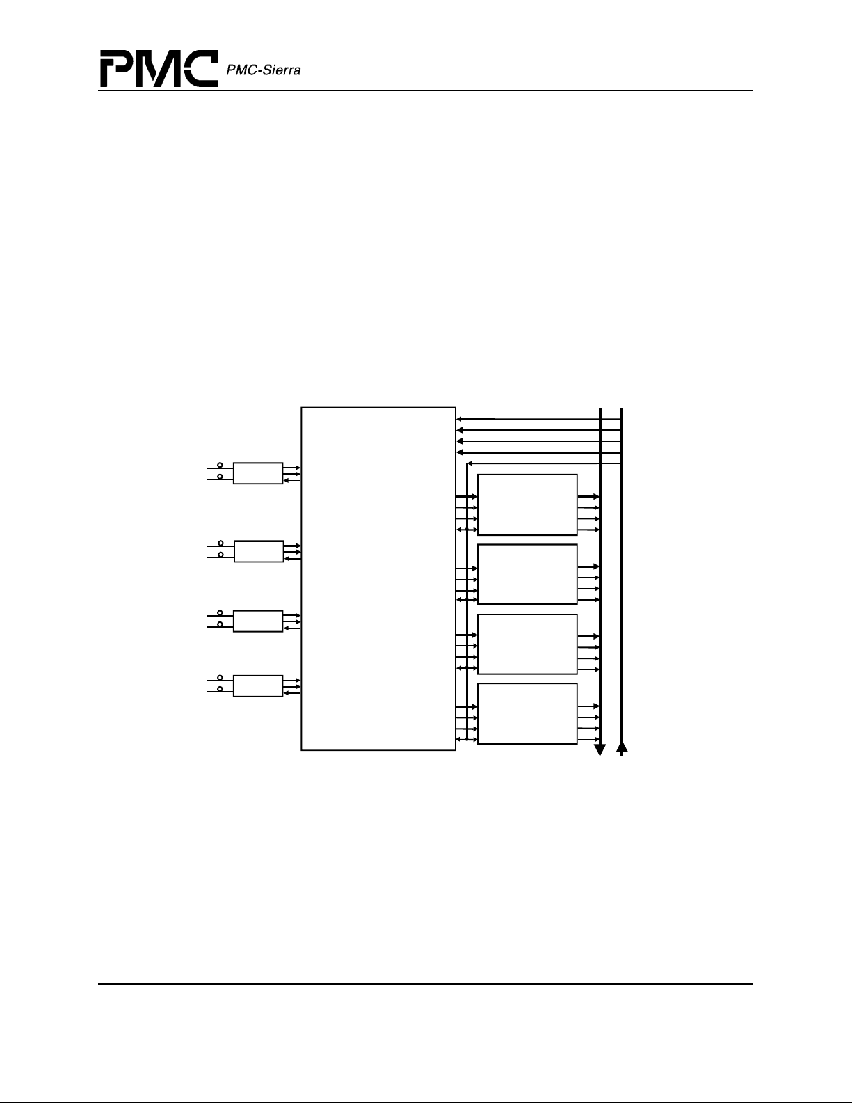
5 Application Examples
The PM5316 SPECTRA-4x155 is designed for use in various SONET/SDH network elements
including switches, terminal multiplexers, and Add/Drop multiplexers. In these applications, the
line interface of the SPECTRA-4x155 typically interfaces directly with the electrical optical
modules and the system side interface connects directly with a TelecomBus.
Figure 1 shows how the SPECTRA-4x155 is used to implement four 155 Mbit/s aggregate
interfaces. In this application, the SPECTRA-4x155 performs SONET/SDH section, line, and
path termination and the PM5362 TUPP-PLUS performs tributary pointer processing and
performance monitoring.
Figure 1 STS-3 (STM-0/AU-3) or STS-3c (STM-1/AU-4) Application with 19.44 MHz Byte
TelecomBus Interface
155 Mbits
Optical
Interface
155 Mbits
Optical
Interface
155 Mbits
Optical
Interface
155 Mbits
Optical
Interface
Optica l
Transceiver
Optica l
Transceiver
Optica l
Transceiver
Optica l
Transceiver
RXD1+/SD1
TXD1+/-
RXD2+/SD2
TXD2+/-
RXD3+/SD3
TXD3+/-
RXD4+/SD4
TXD4+/-
PM5316
SPECTRA-4x155
SONET/SDH Payload Extractor/Aligner (SPECTRA-4x155)
Production
ACK
AD[31:0], ADP[4:1]
AC1J1V1[4:1]
APL[4:1]
PM5362
DD[31:24], DDP[4]
DC1J1V1[4]
DPL[4]
DCK
DD[23:16], DDP[3]
DC1J1V1[3]
DPL[3]
DCK
DD[15:8], DDP[2]
DC1J1V1[2]
DPL[2]
DCK
DD[7:0], DDP[1]
DC1J1V1[1]
DPL[1]
DCK
ID[7:0], IDP
IC1J 1
IPL
SCLK
ID[7:0], IDP
IC1J 1
IPL
SCLK
ID[7:0], IDP
IC1J 1
IPL
SCLK
ID[7:0], IDP
IC1J 1
IPL
SCLK
TUPP-PLUS
PM5362
TUPP-PLUS
PM5362
TUPP-PLUS
PM5362
TUPP-PLUS
OD[7:0], ODP
OTV5
OTPL
TPOH
OD[7:0], ODP
OTV5
OTPL
TPOH
OD[7:0], ODP
OTV5
OTPL
TPOH
OD[7:0], ODP
OTV5
OTPL
TPOH
Four
19.44 M Hz
8-bit
IEEE P1396
Telecombus
Interfaces
Drop Add
The system side interface of the SPECTRA-4x155 can be configured to have a 77.76 MHz byte
TelecomBus interface. Figure 2 shows how the SPECTRA-4x155 is used to implement a 622
Mbit/s aggregate interface using the high-speed TelecomBus on the system side interface. In this
application, the SPECTRA-4x155 performs SONET/SDH section, line, and path termination.
Proprietary and Confidential to PMC-Sierra, Inc. and for its customers’ internal use 8
Document ID: PMC-1990822, Issue 4
Page 28
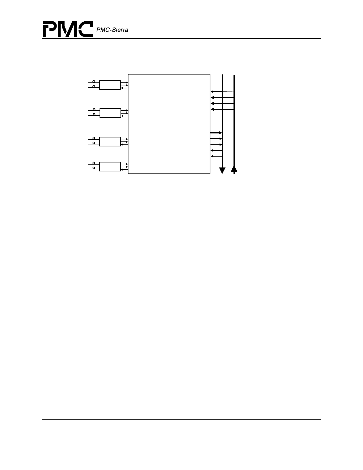
SONET/SDH Payload Extractor/Aligner (SPECTRA-4x155)
Production
Figure 2 STS-3 (STM-1/AU-3) or STS-3c (STM-1/AU-4) Application with 77.76 MHz Byte
TelecomBus Interface
155 Mbits
Optical
Interface
155 Mbits
Optical
Interface
155 Mbits
Optical
Interface
155 Mbits
Optical
Interface
Optical
Transceiver
Optical
Transceiver
Optical
Transceiver
Optical
Transceiver
RXD1 +/-
SD1
TXD1+/-
RXD2 +/SD2
TXD2+/-
RXD3 +/SD3
TXD3+/-
RXD4 +/-
SD4
TXD4+/-
AD[31:0], ADP[4:1]
SPECT RA-4x155
DD[31:0], DDP[4:1]
ACK
AC1J1V1[4:1]
APL[4:1]
DC1J1V1[4:1]
DPL[4:1]
DCK
DFP
Drop Add
77.76 MHz
8-bit
High Speed
Telecombus
Interface
The SPECTRA-4x155 can also be used to implement OC-3 interfaces on channelized high speed
IP switches and routers.
Proprietary and Confidential to PMC-Sierra, Inc. and for its customers’ internal use 9
Document ID: PMC-1990822, Issue 4
Page 29
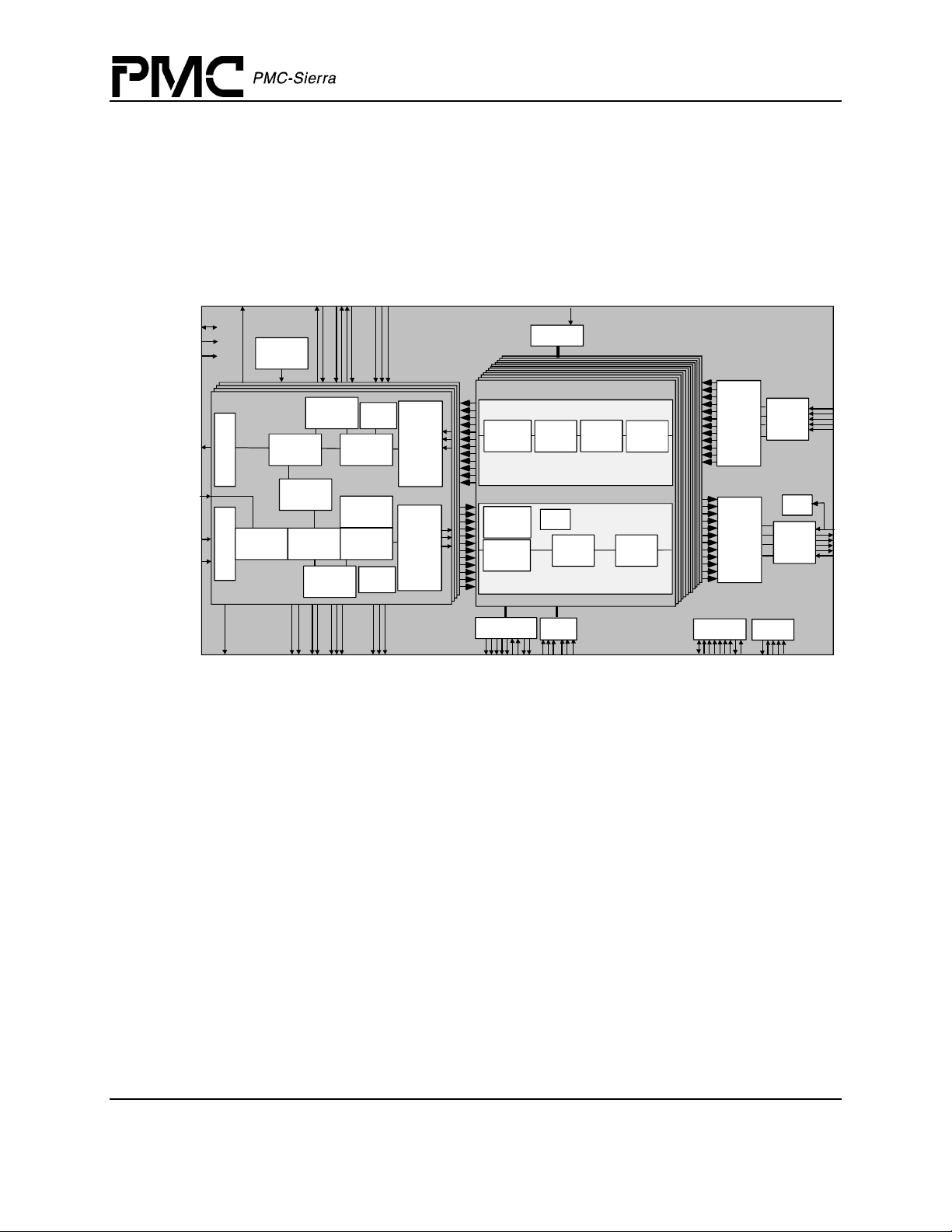
6 Block Diagram
Figure 3 Block Diagram
K
L
ATP[3:0]
PECLV
REFCLK+/-
TXD+/-[4:1]
CP/CN[4:1]
RXD+/ -[4:1 ]
SD[4:1]
C
T
M
G
P
,
K
L
C
T
Channel Line Side Top #m
m={1,2,3,4]
Tx Line
I/F
Clock and
Data
Rx Line
Recovery
I/F
(CRSI)
Synthesis
Clock
(CSPI)
Section O/H
Processor
(TSOP)
Tx
Section
Trace
Buffe r
(SSTB)
Section O/H
Processor
Tx Transport
Rx
(RSOP)
Rx Transport
]
1
:
4
[
]
K
1
:
L
4
C
[
D
D
L
L
S
S
T
T
Overhead
Controller
(TTOC)
Overhead
Controller
(RTOC)
]
1
]
]
:
1
1
4
:
:
[
]
4
4
K
[
[
1
:
L
N
P
4
C
F
[
E
H
H
H
H
O
O
O
O
T
T
T
T
T
T
T
T
Line O/H
Processor
(TLOP)
Receive APS,
Synchronization
Extractor and
Bit Er ror Moni tor
(RASE)
Line O/H
Processor
(RLOP)
]
1
:
4
[
P
F
P
C
R
T
/
I
D
R
L
T
Tx Ri ng
Control Port
(TRCP)
Tx
Rx
Rx Rin g
Control Port
(RRCP)
]
1
:
4
[
K
L
C
P
C
R
T
/
S
I
A
L
R
]
1
:
4
[
T
A
D
P
C
R
T
/
S
I
A
L
T
(TX_REMUX)
(RX_DEMUX)
SONET/SDH Payload Extractor/Aligner (SPECTRA-4x155)
Production
K
C
A
T
,
P
F
A
T
,
D
A
T
TPOC
Path Processing Slice #n
n={1,2..12]
Add Bus
System
Interf ace
DROP
DLL
Rx Telecombus
System
Interfa ce
Tx Path O/H
Processor
(TPOP)
Transmit Path Processing
Slice (TPPS)
Path Trace Buffer
(SPTB)
Rx Pat h O/H
Processor
(RPOP)
Receive Path Processing
Slice (RPPS)
Tx Telecom
Aligner
(TTAL)
PMON
Rx Telecom
Aligner
(RTAL)
ADD Bus
PRBS
Generator/
Monitor
(APGM)
Tx Pointer
Interpreter
DROP Bus
PRBS
Generator/
Monitor
(DPGM)
ADD_TSI
(TPIP)
DROP_TSI
ACK
AC1J1V1[4:1]/AFP[4:1]
APL[4:1]
AD[31:0]
ADP[4:1]
DCK
DC1J1V1[4:1]
DPL[4:1]
DD[31:0]
DDP[4:1]
DFP
DPAIS
RPOC
]
]
]
]
1
:
4
[
K
L
C
R
,
K
L
C
R
M
G
P
]
]
1
1
1
1
1
:
:
:
:
:
4
4
4
4
4
[
[
[
[
[
F
H
K
D
M
O
L
L
L
O
L
S
C
T
A
R
D
R
S
L
S
R
]
]
]
]
]
1
1
1
1
:
4
[
P
F
H
O
T
R
:
4
4
4
4
[
[
[
[
T
P
K
K
L
A
F
L
P
C
D
C
P
C
H
P
C
R
C
O
R
R
T
R
/
R
R
R
/
/
S
I
S
O
I
D
L
A
R
L
L
1
:
:
:
P
K
H
F
L
O
H
C
P
O
H
R
P
O
R
P
R
and
TPAIS
D
N
N
E
H
P
M
E
E
L
H
C
A
T
O
R
R
P
R
S
K
P
S
K
I
I
3
A
F
O
C
T
R
F
C
C
A
A
B
S
R
S
S
I
S
I
P
P
I
I
A
T
A
A
D
A
P
P
P
P
D
T
D
T
Microprocessor
I/F
]
]
E
B
E
0
0
B
L
:
:
S
/
3
7
A
W
C
[
1
B
[
R
D
D
/
A
R
B
R
W
JTAG Test
Access Port
I
B
S
B
B
T
T
N
S
I
R
B
O
K
D
T
E
D
C
M
T
S
T
T
T
B
R
M
T
Proprietary and Confidential to PMC-Sierra, Inc. and for its customers’ internal use 10
Document ID: PMC-1990822, Issue 4
Page 30

7 Functional Description
The PM5316 SPECTRA 4X155 SONET/SDH Payload Extractor/Aligner terminates the transport
and path overhead of four STS-3 (STM-1/AU-3) and STS-3c (STM-1/AU-4) streams at 155
Mbit/s. The device implements significant receive and transmit functions for a SONET/SDHcompliant line interface.
In the receive direction, the SPECTRA-4x155 receives SONET/SDH frames via bit serial
interfaces, recovers clock and data, and terminates the SONET/SDH section (regenerator section),
line (multiplexer section), and path. The device performs framing (A1, A2), descrambling, alarm
detection, and section and line bit interleaved parity (BIP) (B1, B2) monitoring, accumulating
error counts at each level for performance monitoring purposes. The B2 errors are monitored to
detect signal fail and degrade threshold crossing alarms. As part of this process, the device
accumulates line REIs (M1) and may buffer and compare the 16 or 64-byte section trace (J0)
message against the expected message.
The device also interprets the received payload pointers (H1, H2), detects path alarm conditions,
and detects and accumulates path BIPs (B3). The path REIs are monitored and accumulated.
Also, the 16 or 64-byte path trace (J1) message is accumulated and compared against the
expected result. The device then extracts the SPE (VC). All transport and path overhead bytes are
extracted and serialized on lower rate interfaces, allowing additional external processing of
overhead, if desired.
SONET/SDH Payload Extractor/Aligner (SPECTRA-4x155)
Production
The extracted SPE (VC) is placed on a Telecom Drop bus. Frequency offsets, for exampe, due to
plesiochronous network boundaries, or the loss of a primary reference timing source, and phase
differences, due to normal network operation, between the received data stream and the Drop bus
are accommodated by pointer adjustments in the Drop bus.
In the transmit direction, the SPECTRA-4x155 transmits SONET/SDH frames, via bit serial
interfaces, and formats section (regenerator section), line (multiplexer section), and path overhead
appropriately. The device provides transmit path origination for a SONET/SDH STS-3 (STM1/AU-3) or STS-3c (STM-1/AU-4) stream. It performs framing pattern insertion (A1, A2),
scrambling, alarm signal insertion, and creates section and line BIPs (B1, B2) as required to allow
performance monitoring at the far end. Line REIs (M1) and a 16 or 64-byte section trace (J0)
message may be optionally inserted. The device also generates the transmit payload pointers (H1,
H2) and creates and inserts the path BIP. A 16 or 64-byte path trace (J1) message and the path
status byte (G1) is optionally inserted.
In Addition to its basic processing of the transmit SONET/SDH overhead, the SPECTRA-4x155
provides convenient access to all overhead bytes, which are inserted serially on lower rate
interfaces, allowing additional external sourcing of overhead, if desired. The SPECTRA-4x155
also supports the insertion of a large variety of errors into the transmit stream, such as framing
pattern errors and BIP errors, which are useful for system diagnostics and tester applications.
Proprietary and Confidential to PMC-Sierra, Inc. and for its customers’ internal use 11
Document ID: PMC-1990822, Issue 4
Page 31

SONET/SDH Payload Extractor/Aligner (SPECTRA-4x155)
Production
The inserted SPE (VC) is sourced from a TelecomBus Add stream. The SPECTRA-4x155 maps
the SPE (VC) from a Telecom Add bus into the transmit stream. As with the TelecomBus Drop
stream, frequency offsets and phase differences between the transmit data stream and the Add bus
are accommodated by pointer adjustments in the transmit stream.
The SPECTRA-4x155 supports Time-Slot Interchange (TSI) on the Telecom Add and Drop
buses. On the Drop side, the TSI views the receive stream as 12 independent time-division
multiplexed columns of data (12 constituent STS-1 (STM-0/AU-3) or equivalent streams or timeslots or columns). Any column can be connected to any time-slot on the Drop bus, independently
of the channel they originate from. Both column swapping and broadcast are supported. TSI is
independent of the underlying payload mapping formats. Similarly, on the Add side, data from the
Add bus is treated as 12 independent time-division multiplexed columns. Assignment of data
columns to transmit time-slots (STS-1 (STM-0/AU-3) or equivalent streams) is arbitrary.
The transmitter and receiver are independently configurable to allow for asymmetric interfaces.
Ring control ports are provide to pass control and status information between mate transceivers.
The SPECTRA-4x155 is configured, controlled and monitored via a generic 8-bit microprocessor
bus interface.
The SPECTRA-4x155 is implemented in low power, +3.3 Volt, CMOS technology. It has TTL
and pseudo ECL (PECL) compatible inputs and outputs and is packaged in a 520 pin SBGA
package.
Proprietary and Confidential to PMC-Sierra, Inc. and for its customers’ internal use 12
Document ID: PMC-1990822, Issue 4
Page 32
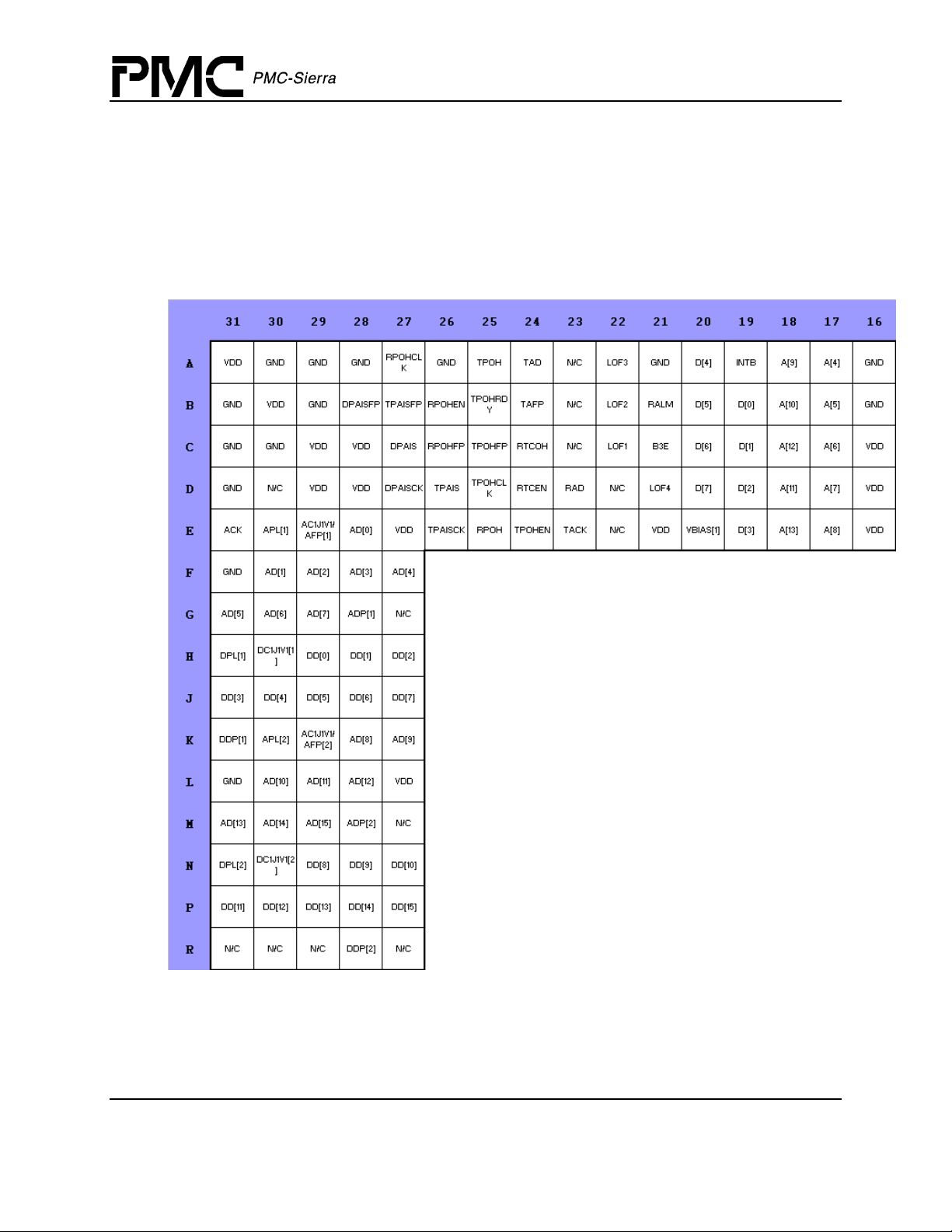
8 Pin Diagrams
The SPECTRA-4x155 is available in a 520 pin SBGA package having a body size of 40 mm by
40 mm and a ball pitch of 1.27 mm.
Figure 4 Pin diagram of SPECTRA-4x155 (Bottom Top right going clockwise)
SONET/SDH Payload Extractor/Aligner (SPECTRA-4x155)
Production
Proprietary and Confidential to PMC-Sierra, Inc. and for its customers’ internal use 13
Document ID: PMC-1990822, Issue 4
Page 33

SONET/SDH Payload Extractor/Aligner (SPECTRA-4x155)
Production
Proprietary and Confidential to PMC-Sierra, Inc. and for its customers’ internal use 14
Document ID: PMC-1990822, Issue 4
Page 34

SONET/SDH Payload Extractor/Aligner (SPECTRA-4x155)
Production
Proprietary and Confidential to PMC-Sierra, Inc. and for its customers’ internal use 15
Document ID: PMC-1990822, Issue 4
Page 35

SONET/SDH Payload Extractor/Aligner (SPECTRA-4x155)
Production
Proprietary and Confidential to PMC-Sierra, Inc. and for its customers’ internal use 16
Document ID: PMC-1990822, Issue 4
Page 36

SONET/SDH Payload Extractor/Aligner (SPECTRA-4x155)
9 Pin Description (SBGA 520)
The SPECTRA-4x155 is available in a 520 pin SBGA package having a body size of 40.0 mm by
40.0 mm and a ball pitch of 1.27 mm.
9.1 Serial Line side Interface Signals
Production
Pin Name Type Pin
Function
No.
REFCLK Input B4 The reference clock input (REFCLK) provides a jitter-free 19.44 MHz
reference clock. It is used as the reference clock by both clock
recovery and clock synthesis circuits.
All channels share this pin.
RXD1-RXD1+
RXD2RXD2+
RXD3RXD3+
RXD4RXD4+
SD1
SD2
SD3
SD4
TXD1TXD1+
TXD2TXD2+
TXD3TXD3+
TXD4TXD4+
TCLK Output C6 The transmit byte clock (TCLK) output provides a timing reference
Diff PECL
Input
SingleEnded
PECL Input
Diff. TTL
Output
(Externally
converted
to PECL
)
K3
K2
M2
M1
Y2
Y1
AB2
AB3
K4
M3
Y3
AB1
J2
J3
L2
L3
W3
W2
AA3
AA2
The receive differential data inputs (RXD[4:1]+, RXD[4:1]-) contain
the 155.52 Mbit/s receive STS-3/3c (STM-1/AU-3/AU-4) stream of
each channel. The receive clocks are recovered from the RXD+/- bit
stream.
RXD[4:1]+/- inputs are expected to be NRZ encoded.
The Signal Detect pin (SD[4:1]) indicates the presence of valid
receive signal power from the Optical Physical Medium Dependent
Device. A PECL high indicates the presence of valid data and a
PECL low indicates a Loss of Signal (LOS). It is mandatory that
SD[4:1] be terminated into the equivalent network that RXD1-4+/- is
terminated into.
This pin is available independently for each channel.
The transmit differential data outputs (TXD[4:1]+, TXD[4:1]-) contain
the 155.52 Mbit/s transmit STS-3/3c (STM-1/AU-3/AU-4) stream.
TXD[4:1]+/- outputs are NRZ encoded.
for the SPECTRA-4x155 self-timed channels. TCLK always provides
a divide-by-eight of the synthesized line rate clock and thus has a
nominal frequency of 19.44 MHz.
TCLK does not apply to internally loop-timed channels, in which case
the channel’s RCLK1-4 provides transmit timing information.
When not used, TCLK can be held low using the TCLKEN bit in the
SPECTRA-4x155 Clock Control register.
Proprietary and Confidential to PMC-Sierra, Inc. and for its customers’ internal use 17
Document ID: PMC-1990822, Issue 4
Page 37

SONET/SDH Payload Extractor/Aligner (SPECTRA-4x155)
Production
Pin Name Type Pin
Function
No.
RCLK1
RCLK2
RCLK3
RCLK4
PGMRCLK Output D6
PGMTCLK Output E6 The programmable transmit clock (PGMTCLK) signal provides timing
CP1
CN1
CP2
CN2
CP3
CN3
CP4
CN4
PECLV Input D2 The PECL receiver input voltage (PECLV) pin configures the PECL
Output
Analog
C7
D7
B6
E7
G2
G3
N3
N2
U3
U2
AD2
AD3
The Receive Clock (RCLK1-4) signal provides a timing reference for
the SPECTRA-4x155 receive line interface outputs. The signal is
nominally 19.44 MHz. It is a divide-by-eight of the recovered clock.
When not used, RCLK1-4 can be held low using the RCLKEN bit in
the SPECTRA-4x155 Clock Control register.
The programmable receive clock (PGMRCLK) signal provides timing
reference for the receive line interface.
PGMRCLK is a divided version of one of the RCLK clocks. The
PGMRCHSEL bits of the Master Clock Control register are used to
select which of the four clocks is the source for PRGMRCLK. When
the PGMRCLKSEL bit of the Master Clock Control register is set low,
PGMRCLK is a nominal 19.44 MHz, 40-60% duty cycle clock. When
PGMRCLKSEL register bit is set to high, PGMRCLK is a nominal 8
KHz, 40-60% duty cycle clock.
PGMRCLK output can be disabled and held low by programming the
PGMRCLKEN bit in the Master Clock Control register.
reference for the transmit line interface.
PGMTCLK is a divided version of the TCLK clock. When the
PGMTCLKSEL register bit is set low, PGMTCLK is a nominal 19.44
MHz, 40-60% duty cycle clock. When the PGMTCLKSEL bit of the
Master Clock Control register is set high, PGMTCLK is a nominal 8
KHz, 40-60% duty cycle clock.
PGMTCLK output can be disabled and held low by programming the
PGMTCLKEN bit in the Master Clock Control register.
The analog CP1-4 and CN1-4 pins are provided for applications that
must meet SONET/SDH jitter transfer specifications. A 220 nF X7R
10% ceramic capacitor can be attached across each CP1-4 and
CN1-4 pair.
receiver level shifter. When PECLV is set to logic zero, the PECL
receivers are configured to operate with a 3.3V input voltage. When
PECLV is set to logic one, the PECL receivers are configured to
operate with a 5.0 V input voltage.
Proprietary and Confidential to PMC-Sierra, Inc. and for its customers’ internal use 18
Document ID: PMC-1990822, Issue 4
Page 38

SONET/SDH Payload Extractor/Aligner (SPECTRA-4x155)
9.2 Section/Line/Path Status and Alarm Signals
Production
Pin Name Type Pin
No.
SALM1
SALM2
SALM3
SALM4
LOF1
LOF2
LOF3
LOF4
LOS1/
LOS2/
LOS3/
LOS4/
/RRCPFP1
/RRCPFP2
/RRCPFP3
/RRCPFP4
Output
Output C22
Output
A13
B13
C13
D13
B22
A22
D21
E13
C12
B11
A10
E13
C12
B11
A10
Function
The section alarm (SALM1-4) output may be set high when an OOF,
LOS, LOF, LAIS, LRDI, section trace identifier mismatch (RS-TIM),
section trace identifier unstable (RS-TIU), signal fail (SF) or signal
degrade (SD) alarm is detected. Each alarm indication can be
independently enabled using bits in the Section Alarm Output Control
#1 and #2 registers. SALM1-4 is set low when none of the enabled
alarms are active.
SALM1-4 is updated on the rising edge of RCLK1-4.
The Loss of Frame (LOF1-4) output is set high when an OOF
condition exists for a total OOF period of 3 ms during which there is
no continuous, in-frame period of 3 ms. LOF1-4 is cleared when an
in-frame condition exists for a continuous period of 3 ms
The LOF1-4 output is updated on the rising edge of RCLK1-4
Loss of Signal (LOS1-4) is active when the ring control port is
disabled. LOS1-4 is set high when a violating period (20 ± 2.5 µs) of
consecutive all zeros patterns is detected in the incoming stream.
LOS1-4 is set low when two valid framing words (A1, A2) are
detected, and during the intervening time (125 µs), there are no other
violating period with all zeros patterns is observed.
LOS1-4 is updated on the rising edge of RCLK1-4.
The Receive ring control port frame position (RRCPFP1-4) signal
identifies bit positions in the receive ring control port data
(RRCPDAT1-4) when the ring control port is enabled. RRCPFP1-4 is
set high during the filtered K1 and K2 bit positions, the change of
APS value bit position, the protection switch byte failure bit position,
and the send line AIS and send line RDI bit positions of the
RRCPDAT1-4 streams (21 bits). RRCPFP1–4 is set low during the
reserved L-REI clock cycles. RRCPFP1-4 can be connected directly
to the TRCPFP1-4 inputs of a mate SPECTRA-4x155 in ring-based
Add/Drop multiplexer applications.
The RCPEN bit in the Ring Control register of the corresponding
channel controls the enabling and disabling of the ring control port.
The RRCPFP1-4 signal is updated on the falling edge of
RRCPCLK1-4.
Proprietary and Confidential to PMC-Sierra, Inc. and for its customers’ internal use 19
Document ID: PMC-1990822, Issue 4
Page 39

SONET/SDH Payload Extractor/Aligner (SPECTRA-4x155)
Production
Pin Name Type Pin
No.
LRDI1/
LRDI2/
LRDI3/
LRDI4/
/RRCPCLK1
/RRCPCLK2
/RRCPCLK3
/RRCPCLK4
LAIS1/
LAIS2/
LAIS3/
LAIS4/
/RRCPDAT1
/RRCPDAT2
/RRCPDAT3
/RRCPDAT4
Output
Output B12
A12
D12
C11
B10
A12
D12
C11
B10
E12
D11
C10
B12
E12
D11
C10
Function
The RDI (LRDI1-4) signal is active when the ring control port is
disabled. LRDI1-4 is set high when line RDI is detected in the
corresponding incoming stream. LRDI is declared when the 110
binary pattern is detected in bits 6, 7, and 8 of the K2 byte for three
or five consecutive frames. LRDI is removed when any pattern other
than 110 is detected in bits 6, 7, and 8 of the K2 byte for three or five
consecutive frames.
The LRDIDET bit in the RLOP Control and Status register of the
corresponding channel controls the selection of three or five
consecutive frames.
LRDI1-4 is updated on the rising edge of RCLK1-4.
The Receive ring control port clock (RRCPCLK1-4) signal provides
timing for the receive ring control port when the ring control port is
enabled. RRCPCLK1-4 is nominally a 3.24 MHz clock and can be
connected directly to the TRCPCLK1-4 inputs of a mate SPECTRA4x155 in ring-based Add-Drop multiplexer applications.
The RCPEN bit in the Ring Control register of the corresponding
channel controls the enabling and disabling of the ring control port.
The RRCPFP1-4 and RRCPDAT1-4 signals are updated on the
falling edge of RRCPCLK1-4.
The line alarm indication (LAIS1-4) signal is active when the ring
control port is disabled. LAIS1-4 is set high when line AIS is detected
in the corresponding incoming stream. Line AIS is declared when the
111 binary pattern is detected in bits 6, 7, and 8 of the K2 byte for
three or five consecutive frames. Line AIS is removed when any
pattern other than 111 is detected in bits 6, 7, and 8 of the K2 byte
for three or five consecutive frames.
The LAISDET bit in the RLOP Control and Status register of the
corresponding channel controls the selection of three or five
consecutive frames.
The LAIS1-4 outputs are updated on the rising edge of RCLK1-4.
The Receive ring control port data (RRCPDAT1-4) signal contains
the receive ring control port data stream when the ring control port is
enabled. The receive ring control port data consists of the filtered K1,
K2 byte values, the change of APS value bit position, the protection
switch byte failure status bit position, the send line AIS and send line
RDI bit positions, and the line REI bit positions. RRCPDAT1-4 can
be connected directly to the TRCPDAT1-4 inputs of a mate
SPECTRA-4x155 in ring-based Add-Drop multiplexer applications.
The RCPEN bit in the Ring Control register of the corresponding
channel controls the enabling and disabling of the ring control port.
The RRCPDAT1-4 signal is updated on the falling edge of
RRCPCLK1-4.
Proprietary and Confidential to PMC-Sierra, Inc. and for its customers’ internal use 20
Document ID: PMC-1990822, Issue 4
Page 40

SONET/SDH Payload Extractor/Aligner (SPECTRA-4x155)
Production
Pin Name Type Pin
No.
RLAIS1/
RLAIS2/
RLAIS3/
RLAIS4/
/TRCPCLK1
/TRCPCLK2
/TRCPCLK3
/TRCPCLK4
Input
D10
B9
A8
C8
D10
B9
A8
C8
Function
The receive line AIS insertion (RLAIS1-4) signal controls the
insertion of line AIS in the received stream by the RSOP block, when
the ring control port is disabled. When one of the RLAIS1-4 pins is
set high, line AIS is inserted in the corresponding received stream.
When RLAIS1-4 is set low, line AIS may be optionally inserted
automatically upon detection of LOS, LOF, section trace alarms or
line AIS in the incoming stream.
The Receive LAIS Control register contains the register bits that
control the alarms that are inserted using the RLAIS pin of the
corresponding channel. RLAIS signals are internally retimed.
RLAIS1-4 must be asserted for a minimum period of one
SONET/SHD frame (125 us) to be detected by the SPECTRA-4x155.
Line AIS must be held for a minimum of three SONET/SDH frames
to be compliant to the SONET/SDH standards.
The Transmit ring control port clock (TRCPCLK1-4) signal provides
timing for the transmit ring control port when the ring control port is
enabled. The TRCPCLK1-4 signal is nominally a 3.24 MHz clock and
can be connected directly to the RRCPCLK output of a mate
SPECTRA-4x155 in ring-based Add/Drop multiplexer applications.
The RCPEN bit in the Ring Control register of the corresponding
channel controls the enabling and disabling of the ring control port.
The TRCPFP1-4 and TRCPDAT1-4 signals are sampled on the
rising edge of TRCPCLK1-4.
Proprietary and Confidential to PMC-Sierra, Inc. and for its customers’ internal use 21
Document ID: PMC-1990822, Issue 4
Page 41

SONET/SDH Payload Extractor/Aligner (SPECTRA-4x155)
Production
Pin Name Type Pin
No.
TLRDI1/
TLRDI2/
TLRDI3/
TLRDI4/
/TRCPFP1
/TRCPFP2
/TRCPFP3
/TRCPFP4
Input
A9
C9
E9
D8
A9
C9
E9
D8
Function
The active high transmit RDI (TLRDI1-4) signal controls the insertion
of a remote defect indication in the transmit outgoing stream when
the ring control port is disabled. When TLRDI1-4 is set high, bits 6, 7,
and 8 of the K2 byte are set to the pattern 110. When TLRDI1-4 is
set low, line RDI may also be inserted using the LRDI bit in the TLOP
Control register of the corresponding channel. Line RDI may also be
inserted upon detection of LOS, LOF, or line AIS in the receive
stream, using the bits in the Transmit Line RDI Control register of the
corresponding channel. The TLRDI1-4 input takes precedence over
the TTOH1-4 and TTOHEN1-4 inputs. TLRDI signals are internally
retimed. TLRDI1-4 must be asserted for a minimum period of one
SONET/SHD frame (125 us) to be detected by the SPECTRA-4x155.
Line RDI must be held for a minimum of three SONET/SDH frames
to be compliant to the SONET/SDH standards.
The Transmit ring control port frame position (TRCPFP1-4) signal
identifies bit positions in the transmit ring control port data
(TRCPDAT1-4) when the ring control port is enabled. TRCPFP1-4 is
high during the send line AIS and the send line RDI bit positions in
the TRCPDAT1-4 stream. TRCPFP1-4 is set high for 19 bits
locations prior to those 2 bit locations. These 19 bit locations are
reserved. TRCPFP1–4 is set low during the reserved L-REI clock
cycles. TRCPFP1-4 can be connected directly to the RRCPFP1-4
output of a mate SPECTRA-4x155 in ring-based Add-Drop
multiplexer applications.
The RCPEN bit in the Ring Control register of the corresponding
channel controls the enabling and disabling of the ring control port.
The TRCPFP1-4 signal is sampled on the rising edge of TRCPCLK1-
4.
Proprietary and Confidential to PMC-Sierra, Inc. and for its customers’ internal use 22
Document ID: PMC-1990822, Issue 4
Page 42

SONET/SDH Payload Extractor/Aligner (SPECTRA-4x155)
Production
Pin Name Type Pin
No.
TLAIS1/
TLAIS2/
TLAIS3/
TLAIS4/
/TRCPDAT1
/TRCPDAT2
/TRCPDAT3
/TRCPDAT4
Input
E10
D9
B8
A7
E10
D9
B8
A7
Function
The active high transmit AIS (TLAIS1-4) controls the insertion of line
AIS in the transmit outgoing stream when the ring control port is
disabled. When TLAIS1-4 is set high, the complete frame (except the
section overhead or line/regenerator section) is overwritten with the
all-ones pattern (before scrambling). The TLAIS1-4 input takes
precedence over the TTOH1-4 and TTOHEN1-4 inputs. TLAIS
signals are internally retimed.
TLAIS1-4 is required to be asserted for a minimum period of one
SONET/SHD frame (125 us) to be detected by the SPECTRA-4x155.
Line AIS must be held for a minimum of three SONET/SDH frames
to be compliant to the SONET/SDH standards.
The Transmit ring control port data (TRCPDAT1-4) signal contains
the transmit ring control port data stream when the ring control port is
enabled. The transmit ring control port data consists of the send line
AIS and the send line RDI bit positions, and the line REI bit positions.
TRCPDAT1-4 can be connected directly to the RRCPDAT1-4 output
of a mate SPECTRA-4x155 in ring-based Add/Drop multiplexer
applications. The K1/K2, COAPSI, PSBFI and PSBFV position of the
RRCPDAT lines are not used by the TRCPDAT.
The RCPEN bit in the Ring Control register of the corresponding
channel controls the enabling and disabling of the ring control port.
TRCPDAT1-4 is sampled on the rising edge of TRCPCLK1-4.
9.3 Receive Section/Line/Path Overhead Extraction Signals
Pin Name Type Pin
No.
RTOHCLK1
RTOHCLK2
RTOHCLK3
RTOHCLK4
RTOH1
RTOH2
RTOH3
RTOH4
Output
Output AK7
AJ7
AL8
AK10
AK12
AH9
AL10
AL12
Function
The receive transport overhead clock (RTOHCLK1-4) output is used
to update the received transport overhead outputs (RTOH1-4 and
RTOHFP1-4).
RTOHCLK1-4 is nominally a 5.184 MHz clock generated by gapping
a 6.48 MHz clock. RTOHCLK1-4 has a 33% high duty cycle.
The RTOHFP1-4 and RTOH1-4 outputs are updated on the falling
edge of RTOHCLK1-4.
The receive transport overhead (RTOH1-4) bit serial output signal
contains the received transport overhead bytes (A1, A2, J0, Z0, B1,
E1, F1, D1-D3, H1-H3, B2, K1, K2, D4-D12, Z1/S1, Z2/M1, and E2)
from the incoming stream.
The RTOH1-4 output is updated on the falling edge of RTOHCLK1-4
and should be sampled externally on the rising edge of RTOHCLK1-
4.
Proprietary and Confidential to PMC-Sierra, Inc. and for its customers’ internal use 23
Document ID: PMC-1990822, Issue 4
Page 43

SONET/SDH Payload Extractor/Aligner (SPECTRA-4x155)
Production
Pin Name Type Pin
Function
No.
RTOHFP1
RTOHFP2
RTOHFP3
RTOHFP4
RPOHCLK Output A27 The receive path overhead clock (RPOHCLK1-4) provides timing to
RPOHFP Output C26 The receive path overhead frame position signal (RPOHFP) may be
RPOH Output E25 The receive path overhead data signal (RPOH) contains the path
RPOHEN Output B26
Output
AH7
AG9
AJ10
AJ12
The receive transport overhead frame position (RTOHFP1-4) signal
is used to locate the most significant bit (MSB) on the RTOH1-4
serial stream.
RTOHFP1-4 is set high when bit 1 (the most significant bit) of the
first framing byte (A1) is present in the RTOH1-4 stream.
RTOHFP1-4 can also be sampled on the rising edge of RSLDCLK14 to locate the MSB of the RSLD1-4 serial output stream. The
generation of this clock is aligned with the generation of RTOHFP1-
4.
RTOHFP1-4 is updated on the falling edge of RTOHCLK1-4.
process the B3E signal, receive alarm port (RAD), path Z5 growth
byte (tandem path incoming error count and data link), and to sample
the extracted path overhead of the four STS-3/3c (STM-1/AU-3/AU-
4) streams. RPOHCLK is a nominally 12.96 MHz, 50% duty cycle
clock.
RTCEN and RTCOH are sampled on the rising edge of the
RPOHCLK signal.
B3E, RAD, RALM, RPOH, RPOHEN and RPOHFP are updated on
the falling edge of the RPOHCLK signal.
used to locate the individual path overhead bits in the path overhead
data stream (RPOH). RPOHFP signal is logic one when bit 1 (the
most significant bit) of the path trace byte (J1) of channel one’s first
STS-1 (STM-0/AU-3) or STS-3c (STM-1/AU-4) is present in the
RPOH stream.
RPOHFP may also be used to locate the BIP error count and path
RDI indication bits on the receive alarm port data signal (RAD).
RPOHFP is logic one when the first of eight BIP error positions of
channel one’s first STS-1 (STM-0/AU-3) or STS-3c (STM-1/AU-4)
stream is present on the receive alarm data signal (RAD).
RPOHFP is also used to help find the alignment of the B3E output
and RTCEN/RTCOH inputs.
RPOHFP signal is updated on the falling edge of the RPOHCLK
signal.
overhead bytes (J1, B3, C2, G1, F2, H4, Z3, Z4, and Z5) extracted
from the path overhead of the three STS-1 (STM-0/AU-3) streams or
STS-3c (STM-1/AU-4) streams in all four channels. The
corresponding RPOHEN signal is set high to identify the valid
overhead bytes that are presented.
RPOH is updated on the falling edge of RPOHCLK.
The receive path overhead enable signal (RPOHEN) indicates the
validity of the path overhead bytes extracted to the RPOH from the
path overhead of the three STS-1 (STM-0/AU-3) streams or STS-3c
(STM-1/AU-4) streams in all four channels. When RPOHEN signal is
set high, the corresponding path overhead byte presented on the
RPOH is valid. When RPOHEN is set low, the corresponding path
overhead byte presented on the RPOH is invalid. RPOHEN also
Proprietary and Confidential to PMC-Sierra, Inc. and for its customers’ internal use 24
Document ID: PMC-1990822, Issue 4
Page 44

SONET/SDH Payload Extractor/Aligner (SPECTRA-4x155)
Production
Pin Name Type Pin
Function
No.
validates the B3E output.
RPOHEN is updated on the falling edge of RPOHCLK.
RAD Output The receive alarm port data signal (RAD) contains the path BIP error
count and the path remote alarm indication status of the three STS-1
(STM-0/AU-3) streams or STS-3c (STM-1/AU-4) streams for all four
channels. In Addition, the RAD contains the transmit K1 and K2
bytes of the four transmit streams when not generating AIS-L on the
transmit stream.
RPOHFP is used to determine the alignment of the RAD output.
RAD is updated on the falling edge of RPOHCLK.
B3E Output C21 The bit interleaved parity error signal (B3E) carries the path BIP-8
error detected for each STS-1 (STM-0/AU-3) and STS-3c (STM1/AU-4) in the receive stream. It is set high for one RPOHCLK period
for each path BIP-8 error detected (up to eight per frame) or when
errors are treated on a block basis, is set high for only one
RPOHCLK period if any of the path BIP-8 bits are in error. Path BIP8 errors are detected by comparing the extracted path BIP-8 byte
(B3) with the computed BIP-8 for the previous frame.
The B3E signal toggles during the B3 time periods on RPOH and is
valid only during RPOHEN set high. RPOHFP is used to determine
the alignment of the B3E output.
B3E is updated on the falling edge of RPOHCLK.
RTCEN Input D24 The receive tandem connection overhead insert enable signal
(RTCEN) controls the insertion of incoming error count and data link
into the tandem connection maintenance byte (Z5) on the Drop bus,
on a bit-by-bit basis for each STS-1 (STM-0/AU3) or STS-3c
(STM-1/AU4) stream. When RTCEN is set high, the data on the
corresponding RTCOH stream is inserted into the associated bit in
the Z5 byte. RTCEN has significance only during the J1 byte
positions in the RPOHCLK clock sequence where RPOHEN is also
set high and is ignored at all other times. Setting low the RTC_EN
control bit in the RPOP Z5 Growth Control Register disables the
RTCEN and RTCOH ports completely.
RTCEN is sampled on the rising edge of RPOHCLK.
RTCOH Input C24 The receive tandem connection overhead data signal (RTCOH)
contains the incoming error count and data link message to be
inserted into the tandem connection maintenance byte (Z5) in each
STS-1 (STM-0/AU-3) or STS-3c (STM-1/AU-4) stream. When
RTCEN is set high and RPOHEN is high, the values sampled on
RTCOH are inserted into the Z5 byte of the corresponding stream on
the Drop bus. When RTCEN is set low, the received Z5 byte is
passed through unmodified. Setting low the RTC_EN control bit in
the RPOP Z5 Growth Control Register disables the RTCEN and
RTCOH ports completely.
RTCOH is sampled on the rising edge of RPOHCLK.
RALM Output B21
The Receive Alarm (RALM) signal is a multiplexed output of
individual alarms of the receive STS-1 (STM-0/AU3) or STS-3c
(STM-1/AU4) streams. Each alarm represents the logical OR of the
LOP, PAIS, PRDI, PERDI, LOM, LOPCON, PAISCON, UNEQ,
Proprietary and Confidential to PMC-Sierra, Inc. and for its customers’ internal use 25
Document ID: PMC-1990822, Issue 4
Page 45

SONET/SDH Payload Extractor/Aligner (SPECTRA-4x155)
Production
Pin Name Type Pin
No.
Function
PSLU, PSLM, TIU-P, TIM-P status of the corresponding stream. In
Addition to these alarms, the LOS (LOS), LOF (LOF) or line AIS
(LAIS) in the corresponding STS-3 (STM-1) SONET/SDH streams
can also be reported on RALM. The RPPS RALM Output Control #1
and #2 registers control the selection of alarms to be reported.
RALM is updated on the falling edge of RPOHCLK and may
transition anywhere during the individual STS-1 time slot period.
The loss of pointer signal (LOP) indicates the loss of pointer state in
the corresponding STS-1 (STM-0/AU-3) or STS-3c (STM-1/AU-4)
SONET/SDH stream. LOP is set high when invalid pointers are
received in eight consecutive frames, or if eight consecutive enabled
NDFs are detected in the stream.
The path alarm indication signal (PAIS) indicates the path AIS state
of the corresponding STS-1 (STM-0/AU3) or STS-3c (STM-1/AU4)
SONET/SDH stream. PAIS is set high when an all-ones pattern is
observed in the pointer bytes (H1 and H2) for three consecutive
frames in the stream.
The path remote defect indication signal (PRDI) indicates the path
remote state of the corresponding STS-1 (STM-0/AU-3) or STS-3c
(STM-1/AU-4) SONET/SDH stream. PRDI is set high when the path
RDI alarm bit (bit 5) of the path status (G1) byte is set high for five or
ten consecutive frames. The RDI10 bit in the RPOP Pointer MSB
register controls whether five or ten consecutive frames will cause a
PRDI indication.
The path enhanced remote defect indication signal (PERDI)
indicates the path enhanced remote state of the corresponding STS1 (STM-0/AU-3) or STS-3c (STM-1/AU-4) SONET/SDH stream.
PERDI is set high when the path ERDI alarm code (bits 5,6,7) of the
path status (G1) byte is set to the same alarm codepoint for five or
ten consecutive frames. The RDI10 bit in the RPOP Pointer MSB
register controls whether five or ten consecutive frames will cause a
PRDI indication.
The loss of multiframe signal (LOM) indicates the tributary multiframe
synchronization status of the corresponding STS-1 (STM-0/AU3) or
STS-3c (STM-1/AU-4) SONET/SDH stream. LOM is set high if a
correct four frame sequence is not detected in eight frames.
The loss of pointer concatenation and path AIS concatenation
signals (LOPCON and PAISCON) are the concatenated alarms for
STS-3c (STM-1/AU-4) SONET/SDH streams.
The receive path unequipped status (UNEQ) indicates the
unequipped status of the path signal label of the corresponding STS1 (STM-0/AU-3) or STS-3c (STM-1/AU-4) SONET/SDH stream.
UNEQ is set high when the filtered path signal label indicates
unequipped and is dependent on the selected UNEQ mode.
The receive path signal label unstable status (PSLU) reports the
stable/unstable status (mode 1) of the path signal label in the
corresponding STS-1 (STM-0/AU-3) or STS-3c (STM-1/AU-4)
SONET/SDH stream. PSLU is set high when the current received C2
byte differs from the previous C2 byte for five consecutive frames.
The receive path signal label mismatch (PSLM) status reports the
Proprietary and Confidential to PMC-Sierra, Inc. and for its customers’ internal use 26
Document ID: PMC-1990822, Issue 4
Page 46

SONET/SDH Payload Extractor/Aligner (SPECTRA-4x155)
Production
Pin Name Type Pin
Function
No.
match/mismatch status (mode 1 and mode 2) for the path signal
label of the corresponding STS-1 (STM-0/AU-3) or STS-3c (STM1/AU-4) SONET/SDH stream. In mode 1, PSLM is set high when the
accepted PSL differs from the expected PSL written by the
microprocessor. In mode 2, PSLM is set high when 5 consecutive
mismatches have been declared
The receive path trace identifier unstable status (TIU-P) reports the
stable/unstable status (mode 1 and mode 2) of the path trace
identifier framer of the corresponding STS-1 (STM-0/AU-3) or STS3c (STM-1/AU-4) SONET/SDH stream. In mode 1, TIU is set high
when the current message differs from its immediate predecessor for
eight consecutive frames. In mode 2, TIU is set high when three
consecutive 16-byte windows of trace bytes are detected to have
errors. TIU2 is set low when the same trace byte is received in
forty-eight consecutive SONET/SDH frames.
The receive path trace identifier mismatch (TIM-P) status reports the
match/mismatch status (mode 1) of the path identifier message
framer of the corresponding STS-1 (STM-0/AU-3) or STS-3c (STM1/AU-4) SONET/SDH stream. TIM-P is set high when the accepted
identifier message differs from the expected message written by the
microprocessor.
Please refer to the individual alarm interrupt descriptions and
Functional Description Section for more details on each alarm.
9.4 Transmit Section/Line/Path Overhead Insertion Signals
Pin Name Type Pin
No.
TTOHCLK1
TTOHCLK2
TTOHCLK3
TTOHCLK4
TTOH1
TTOH2
TTOH3
TTOH4
TTOHEN1
TTOHEN2
TTOHEN3
TTOHEN4
Output AG8
AJ9
AH11
AG13
Input AJ8
AL9
AG12
AK13
Input
AH8
AG10
AK11
AJ13
Function
The transmit transport overhead clock (TTOHCLK1-4) is used to
clock in the transport overhead (TTOH1-4) to be transmitted along
with the overhead enable (TTOHEN1-4).
TTOHCLK1-4 is nominally a 5.184 MHz clock generated by gapping
a 6.48 MHz clock. TTOHCLK1-4 has a 33% high duty cycle.
TTOHFP1-4 and TTOH1-4.are updated on the falling edge of
TTOHCLK1-4.
The transmit transport overhead (TTOH1-4) bit serial input signal
contains the transport overhead bytes (A1, A2, J0, Z0, B1, E1, F1,
D1-D3, H1-H3, B2, K1, K2, D4-D12, Z1/S1, Z2/M1, and E2) to be
transmitted and errors masks to be applied on the B1, B2, H1 and
H2 transmitted bytes. Insertion of the bytes must be accompanied
by a high TTOHEN1-4 signal.
TTOH1-4 is sampled on the rising edge of TTOHCLK1-4.
The transmit transport overhead insert enable (TTOHEN1-4) signal
controls the source of the transport overhead data which is inserted
in the outgoing stream. When TTOHEN1-4 is high during bit 1 (most
significant bit) of a TOH byte on TTOH, the sampled TOH byte is
inserted into the corresponding transport overhead byte positions
(A1, A2, J0, Z0, E1, F1, D1-D3, H3, K1, K2, D4-D12, Z1/S1, Z2/M1,
and E2 bytes). While TTOHEN1-4 is low during the most significant
bit of a TOH byte on TTOH, that sampled byte is ignored and the
Proprietary and Confidential to PMC-Sierra, Inc. and for its customers’ internal use 27
Document ID: PMC-1990822, Issue 4
Page 47

SONET/SDH Payload Extractor/Aligner (SPECTRA-4x155)
Production
Pin Name Type Pin
Function
No.
default values are inserted into these transport overhead bytes. The
overhead byte enabled by the TTOHEN input takes precedence
over the TSLD input.
When TTOHEN1-4 is high during the most significant bit of the H1,
H2, B1 or B2 TOH byte positions on TTOH1-4, the sampled TOH
byte is logically XOR’ed with the associated incoming byte to force
bit errors on the outgoing byte. A logic low bit in the TTOH1-4 byte
allows the incoming bit to go through while a bit set to logic high will
toggle the incoming bit. A low level on TTOHEN1-4 during the MSB
of the TOH byte disables the error forcing for the entire byte.
When the transmit trace enable (TREN) bit in the TTOC Transport
Overhead Byte Control register of the corresponding channel is a
logic one, the J0 byte contents are sourced from the section trace
buffer, regardless of the state of TTOHEN1-4.
TTOHEN1-4 is sampled on the rising edge of TTOHCLK1-4.
TTOHFP1
TTOHFP2
TTOHFP3
TTOHFP4
TAD Input A24
TAFP Input B24 The transmit alarm port frame pulse signal (TAFP) marks the first bit
TACK Input E23 The transmit alarm port clock (TACK) provides timing for transmit
Output AL7
AK9
AJ11
AH13
The transmit transport overhead frame position (TTOHFP1-4) signal
is used to locate the most significant bit (MSB) on the TTOH1-4
serial stream.
TTOHFP1-4 is set high when bit 1 (the most significant bit) of the
first framing byte (A1) should be present on the TTOH1-4 stream.
TTOHFP1-4 can be sampled on the rising edges of TSLDCLK1-4 to
locate the MSB of the TSLD serial input stream. The generation of
this clock is aligned with the generation of TTOHFP1-4.
TTOHFP1-4 is updated on the falling edge of TTOHCLK1-4.
The transmit alarm port data signal (TAD) contains the path REI
count and the path RDI status to be inserted into the four STS-3/3c
(STM-1/AU-3/AU-4) streams. In Addition, the TAD input contains
the K1 and K2 bytes from a mate SPECTRA-4x155 to be inserted
into the four channels transport overhead. TAD takes precedence
over TTOHEN1-4 when enabled.
The RXSEL[1:0] bits in the TPPS Path Configuration register control
the source of the transmit P-REI and P-RDI.
TAD is sampled on the rising edge of TACK.
of the transmit alarm message in each SONET/SDH frame. TAFP is
pulsed high to mark the first path REI bit location of channel one’s
first STS-1 (STM-0/AU-3) stream or the first path REI bit location of
the STS-3c (STM-1/AU-4) stream.
TAFP is sampled on the rising edge of TACK.
alarm port. TACK is nominally a 12.96 MHz, 50% duty cycle clock.
Inputs TAD and TAFP are sampled on the rising edge of TACK.
Proprietary and Confidential to PMC-Sierra, Inc. and for its customers’ internal use 28
Document ID: PMC-1990822, Issue 4
Page 48

SONET/SDH Payload Extractor/Aligner (SPECTRA-4x155)
9.5 Receive Section/Line DCC Extraction Signals
Production
Pin Name Type Pin
No.
RSLDCLK1
RSLDCLK2
RSLDCLK3
RSLDCLK4
RSLD1
RSLD2
RSLD3
RSLD4
Tristate
Output
Tristate
Output
AG14
AG15
AL17
AL18
AH14
AH15
AK17
AK18
Function
The receive section or line data communication channel (DCC) clock
(RSLDCLK1-4) is used to update the received section or line DCC
(RSLD1–4).
When selecting to clock the section DCC, RSLDCLK1-4 is a 192 kHz
clock with nominal 50% duty cycle. When selecting to clock the line
DCC, RSLDCLK1-4 is a 576 kHz clock with nominal 50% duty cycle.
RTOHFP1-4 may be sampled high at the same time as bit 1 (MSB)
on RSLD1-4.
The RTOC Overhead Control register of the corresponding channel
contains the RSLDSEL register bit used to select the section or line
DCC. The same register also contains the RSLD_TS register bit that
can be used to tri-state RSLDCLK1-4 and RSLD1-4 outputs.
In both cases, RSLD1-4 is updated on the falling edge of
RSLDCLK1-4.
The receive section or line DCC (RSLD1-4) bit serial output signal
contains the received section data communication channel (D1-D3)
or the line data communication channel (D4-D12).
The RTOC Overhead Control register of the corresponding channel
contains the RSLDSEL register bit used to select the section or line
DCC. The same register also contains the RSLD_TS register bit that
can be used to tri-state RSLDCLK1-4 and RSLD1-4 outputs.
RSLD1-4 is updated on the falling edge of RSLDCLK1-4 and should
be sampled externally on the rising edge of RSLDCLK1-4.
9.6 Transmit Section/Line DCC Insertion Signals
Pin Name Type Pin
No.
TSLDCLK1
TSLDCLK2
TSLDCLK3
TSLDCLK4
TSLD1
TSLD2
TSLD3
TSLD4
Tristate
Output
Input AK14
AJ14
AJ15
AJ17
AJ18
AK15
AH17
AH18
Function
The transmit section or line data communication channel (DCC)
clock (TSLDCLK1-4) is used to clock in the transmit section or line
DCC (TSLD1-4).
When clocking the section DCC, TSLDCLK1-4 is a 192 kHz clock
with nominal 50% duty cycle. When clocking the line DCC,
TSLDCLK1-4 is a 576 kHz clock with nominal 50% duty cycle.
TTOHFP1-4 is used to identify when bit 1 (MSB) of the first A1 byte
should be present on TSLD1-4.
The TTOC Overhead Control register of the corresponding channel
contains the TSLD_SEL register bit used to select the section or
line DCC. The same register also contains the TSLD_TS register bit
that can be used to tri-state the TSLDCLK1-4 output.
In both cases, TSLD1-4 is sampled on the rising edge of
TSLDCLK1-4.
The transmit section or line DCC (TSLD) bit serial input signal
contains the section data communication channel (D1-D3) or the
line data communication channel (D4-D12) to be transmitted.
TTOHFP1-4 is used to identify the required alignment of TSLD.
The TTOH1-4 and TTOHEN1-4 inputs take precedence over
Proprietary and Confidential to PMC-Sierra, Inc. and for its customers’ internal use 29
Document ID: PMC-1990822, Issue 4
Page 49

SONET/SDH Payload Extractor/Aligner (SPECTRA-4x155)
Production
Pin Name Type Pin
Function
No.
TSLD1-4.
The TTOC Overhead Control register of the corresponding channel
contains the TSLD_SEL register bit used to select the section or
line DCC. The same register also contains the TSLD_VAL register
bit used to specify a value for the DCC not inserted via TSLD.
TSLD1-4 is sampled on the rising edge of TSLDCLK1-4.
9.7 Transmit Path AIS Insertion Signals
Pin Name Pin Type Pin
No.
DPAISCK Input D27 The Drop bus path alarm indication clock signal (DPAISCK) provides
DPAISFP Input B28
DPAIS Input C27 The active high Drop bus path alarm indication signal (DPAIS) is a
TPAISCK Input E26 The Transmit path alarm indication clock signal (TPAISCK) provides
Function
timing for system Drop path alarm indication signal (DPAIS).
DPAISCK is a clock of arbitrary phase and frequency within the limits
specified in the A.C. Timing section of this document.
Inputs DPAIS and DPAISFP are sampled on the rising edge of
DPAISCK.
The active high Drop bus path alarm indication frame pulse signal
(DPAISFP) is used to identify the alignment of the DPAIS signal.
DPAISFP is set high to mark the path request of channel one’s the
first Drop bus STS-1 (STM-0/AU-3) stream or STS-3c (STM-1/AU-4)
stream. In the absence of a frame pulse, the device will maintain the
last alignment and wrap around on its own.
DPAISFP is sampled on the rising edge of DPAISCK.
timeslot multiplexed signal that controls the insertion of path alarm
indication signal (PAIS) on the Drop bus (DD[31:24], DD[23:16],
DD[15:8], DD[7:0]) on a per STS-1/STM-1(AU3) or STS3c/STM1(AU4)basis.
A high level on DPAIS during a specific timeslot forces the insertion
of the all-ones pattern into the corresponding SPE and the payload
pointer bytes (H1, H2, and H3) presented on the Drop bus. A high
during the first time slot of a channel carrying an STS-3c/STM1(AU4) stream will force the entire concatenated SPE to all-ones. A
high during the second or third time slot of a channel carrying an
STS-3c/STM-1(AU4) will have no effect.
Path AIS can also be inserted by setting the IPAIS control bit in the
RTAL Control register or in response to receive alarms by the RPPS
Path AIS Control #1 and #2 registers.
DPAIS may be enabled or disabled on a per slice basis via the
DPAIS_EN bit in the RPPS Path AIS Control register #1.
DPAIS is sampled on the rising edge of DPAISCK.
timing for system Add side path alarm indication signal (PAIS)
assertion.
TPAISCK is a clock of arbitrary phase and frequency within the limits
specified in the A.C. Timing section of this document.
Inputs TPAIS and TPAISFP are sampled on the rising edge of
Proprietary and Confidential to PMC-Sierra, Inc. and for its customers’ internal use 30
Document ID: PMC-1990822, Issue 4
Page 50

SONET/SDH Payload Extractor/Aligner (SPECTRA-4x155)
Production
Pin Name Pin Type Pin
Function
No.
TPAISCK.
TPAISFP Input B27
TPAIS Input D26 The active high Transmit path alarm indication signal (TPAIS) is a
The active high Transmit path alarm indication frame pulse signal
(TPAISFP) is used to identify the alignment of the TPAIS signal.
TPAISFP is set high to mark the path request of channel one’s the
first transmit STS-1 (STM-0/AU-3) stream or STS-3c (STM-1/AU-4)
stream. In the absence of a frame pulse, the device will maintain the
last alignment and wrap around on its own.
TPAISFP is sampled on the rising edge of TPAISCK.
timeslot multiplexed signal that controls the insertion of path in the
transmit stream on a per STS-1/STM-1(AU3) or STS-3c/STM1(AU4)
basis.
A high level on TPAIS during a specific timeslot forces the insertion
of the all-ones pattern into the corresponding SPE and the payload
pointer bytes (H1, H2, and H3). A high during the first time slot of a
channel carrying an STS-3c/STM-1(AU4) stream will force the entire
concatenated SPE to all-ones. A high during the second or third time
slot of a channel carrying an STS-3c/STM-1(AU4) will have no effect.
Path AIS can also be inserted by setting the PAIS control bit in the
TTAL Control register or in response to Add Bus alarms by the TPPS
Path AIS Control register.
TPAIS may be enabled or disabled on a per slice basis via the
TPAIS_EN bit in the TPPS Path AIS Control register.
TPAIS is sampled on the rising edge of TPAISCK.
9.8 Drop Bus Telecom Interface Signals
Pin Name Pin Type
Pin
No.
DCK Input AH30 The Drop bus clock (DCK) provides timing for the Drop bus
DFP Input AG29 The active high Drop bus reference frame position signal (DFP)
Function
interface. DCK is nominally a 77.76 MHz, 50% duty cycle clock
when the Drop interface is configured as a single bus interface.
DCK is nominally a 19.44 MHz, 50% duty cycle clock when the Drop
interface is configured as a quad STS-3 (STM-1) interface.
Frequency offsets between line side clock (or divided by 4 version
of) and DCK are accommodated by pointer justification events on
the Drop bus.
DFP is sampled on the rising edge of DCK.
Outputs DPL[4:1], DC1J1V1[4:1], DDP[4:1] and DD[31:0] are
updated on the rising edge of DCK when used.
indicates when the first byte of the synchronous payload envelope
(SPE byte #1) is available on the DD[7:0], DD[15:8], DD[23:16] and
DD[31:24] buses. For the single bus interface the first SPE byte of
channel one STS-1 #1 is identified. For the quad bus STS-3 (STM-
1) interface the first SPE byte of all channels STS-1 #1 on the four
output buses identified. Note that DFP has a fixed relationship to the
SONET/SDH frame; the start of payload is determined by the STS
(AU) pointer and may change relative to DFP. Forced changes of
Proprietary and Confidential to PMC-Sierra, Inc. and for its customers’ internal use 31
Document ID: PMC-1990822, Issue 4
Page 51

SONET/SDH Payload Extractor/Aligner (SPECTRA-4x155)
Production
Pin Name Pin Type Pin
No.
DD[0]
DD[1]
DD[2]
DD[3]
DD[4]
DD[5]
DD[6]
DD[7]
DD[8]
DD[9]
DD[10]
DD[11]
DD[12]
DD[13]
DD[14]
DD[15]
Output H29
H28
H27
J31
J30
J29
J28
J27
Output N29
N28
N27
P31
P30
P29
P28
P27
Function
the Drop bus frame alignment by displacing of the regular DFP
pulse will cause errors and will force the need to resynchronize or
regenerate the RPPS PRBS monitors and generators.
The SPECTRA-4x155 will flywheel in the absence of a DFP pulse.
DFP is sampled on the rising edge of DCK.
In single Drop bus interface mode, the Drop bus data (DD[7:0])
contains the multiplexed STS-3/3c(STM-1/AU-3/AU-4) received
SONET/SDH payload data of all four channels. In quad Drop bus
interface STS-3(STM-1) mode, the Drop bus data (DD[7:0]) contains
the channel one STS-3/3c (STM-1/AU-3/AU-4) received
SONET/SDH payload data. When the Drop bus TSI functionality is
disabled, the Dropped payload multiplexing corresponds to the
SONET/SDH data received on channel #1. TSI may be used to
reorder this multiplexing on the Drop bus. STS-1/STM-1(AU3)’s
within a channel or between channels, along with entire channels
may be swapped. The transport overhead bytes, with the exception
of the H1, H2 pointer bytes and when there are no negative pointer
justifications the H3, are set to zeros. The fixed framing patterns for
the A1 and A2 framing bytes may be inserted. The GEN_A1A2_EN
bit in the DPGM Generator Control #1 register enables insertion of
the A1 and A2 framing bytes. The fixed stuff columns in a tributary
mapped SPE (VC) may also be optionally set to zero or NPI. The
H4BYP and CLRFS bits in the RTAL Control register control the
insertion of the H4 byte and the value of the fixed stuff columns.
DD[7] is the most significant bit (corresponding to bit 1 of each serial
word, the first bit received). DD[0] is the least significant bit
(corresponding to bit 8 of each serial word, the last bit received).
DD[7:0] is updated on the rising edge of DCK. The Drop interface
mode is set via the DTMODE register bit in the Drop Bus
Configuration register.
In single Drop bus interface mode, the Drop bus data (DD[15:8]) is
forced low. In quad Drop bus interface STS-3(STM-1) mode, the
Drop bus data (DD[15:8]) contains the channel two STS-3/3c (STM1/AU-3/AU-4) received SONET/SDH payload data. When the Drop
bus TSI functionality is disabled, the Dropped payload corresponds
to the SONET/SDH data received on channel #2. TSI may be used
to reorder this multiplexing on the Drop bus. STS-1/STM-1(AU3)’s
within a channel or between channels, along with entire channels
may be swapped. The transport overhead bytes, with the exception
of the H1, H2 pointer bytes and when there are no negative pointer
justifications the H3, are set to zeros. The fixed framing patterns for
the A1 and A2 framing bytes may be inserted. The GEN_A1A2_EN
bit in the DPGM Generator Control #1 register enables insertion of
the A1 and A2 framing bytes. The fixed stuff columns in a tributary
mapped SPE (VC) may also be optionally set to zero or NPI. The
H4BYP and CLRFS bits in the RTAL Control register control the
insertion of the H4 byte and the value of the fixed stuff columns.
DD[15] is the most significant bit (corresponding to bit 1 of each
serial word, the first bit received). DD[8] is the least significant bit
(corresponding to bit 8 of each serial word, the last bit received).
DD[15:8] is updated on the rising edge of DCK. The Drop interface
mode is set via the DTMODE register bit in the Drop Bus
Proprietary and Confidential to PMC-Sierra, Inc. and for its customers’ internal use 32
Document ID: PMC-1990822, Issue 4
Page 52

SONET/SDH Payload Extractor/Aligner (SPECTRA-4x155)
Production
Pin Name Pin Type Pin
Function
No.
Configuration register.
DD[16]
DD[17]
DD[18]
DD[19]
DD[20]
DD[21]
DD[22]
DD[23]
DD[24]
DD[25]
DD[26]
DD[27]
DD[28]
DD[29]
DD[30]
DD[31]
DPL[1] Output H31 The active high Drop bus payload active signal #1 (DPL[1])
Output
Output AE31
W27
Y31
Y30
Y29
Y28
Y27
AA30
AA29
AE30
AE29
AE28
AE27
AF30
AF29
AG31
In single Drop bus interface mode, the Drop bus data (DD[23:16]) is
forced low. In quad bus interface STS-3(STM-1) mode, the Drop
bus data (DD[15:8]) contains the channel three STS-3/3c (STM1/AU-3/AU-4) received SONET/SDH payload data. When the Drop
bus TSI functionality is disabled, the Dropped payload corresponds
to the SONET/SDH data received on channel #3. TSI may be used
to reorder this multiplexing on the Drop bus. STS-1/STM-1(AU3)’s
within a channel or between channels, along with entire channels
may be swapped. The transport overhead bytes, with the exception
of the H1, H2 pointer bytes and when there are no negative pointer
justifications the H3, are set to zeros. The fixed framing patterns for
the A1 and A2 framing bytes may be inserted. The GEN_A1A2_EN
bit in the DPGM Generator Control #1 register enables insertion of
the A1 and A2 framing bytes. The H4 byte may also be inserted.
The fixed stuff columns in a tributary mapped SPE (VC) may also be
optionally set to zero or NPI. The H4BYP and CLRFS bits in the
RTAL Control register control the insertion of the H4 byte and the
value of the fixed stuff columns. DD[23] is the most significant bit
(corresponding to bit 1 of each serial word, the first bit received).
DD[16] is the least significant bit (corresponding to bit 8 of each
serial word, the last bit received).
DD[23:16] is updated on the rising edge of DCK. The Drop interface
mode is set via the DTMODE register bit in the Drop Bus
Configuration register.
In single Drop bus interface mode, the Drop bus data (DD[31:24]) is
forced low. In quad bus interface STS-3(STM-1) mode, the Drop
bus data (DD[31:24]) contains the channel four STS-3/3c (STM1/AU-3/AU-4) received SONET/SDH payload data. When the Drop
bus TSI functionality is disabled, the Dropped payload corresponds
to SONET/SDH data received on channel #4. TSI may be used to
reorder this multiplexing on the Drop bus. STS-1/STM-1(AU3)’s
within a channel or between channels, along with entire channels
may be swapped. The transport overhead bytes, with the exception
of the H1, H2 pointer bytes and when there are no negative pointer
justifications the H3, are set to zeros. The fixed framing patterns for
the A1 and A2 framing bytes may be inserted. The GEN_A1A2_EN
bit in the DPGM Generator Control #1 register enables insertion of
the A1 and A2 framing bytes. The H4 byte may also be inserted.
The fixed stuff columns in a tributary mapped SPE (VC) may also be
optionally set to zero or NPI. The H4BYP and CLRFS bits in the
RTAL Control register control the insertion of the H4 byte and the
value of the fixed stuff columns. DD[31] is the most significant bit
(corresponding to bit 1 of each serial word, the first bit received).
DD[24] is the least significant bit (corresponding to bit 8 of each
serial word, the last bit received).
DD[31:24] is updated on the rising edge of DCK. The Drop interface
mode is set via the DTMODE register bit in the Drop Bus
Configuration register.
indicates when the DD[7:0] is carrying a payload byte. It is set high
during path overhead and payload bytes and low during transport
Proprietary and Confidential to PMC-Sierra, Inc. and for its customers’ internal use 33
Document ID: PMC-1990822, Issue 4
Page 53

SONET/SDH Payload Extractor/Aligner (SPECTRA-4x155)
Production
Pin Name Pin Type Pin
Function
No.
overhead bytes. DPL[1] is set high during the H3 byte to indicate a
negative pointer justification event and set low during the byte
following H3 to indicate a positive pointer justification event.
DPL[1] is updated on the rising edge of DCK. The Drop interface
mode is set via the DTMODE register bit in the Drop Bus
Configuration register.
DPL[2] Output N31 The active high Drop bus payload active signal #2 (DPL[2])
indicates when the DD[15:8] is carrying a payload byte. It is set high
during path overhead and payload bytes and low during transport
overhead bytes. DPL[2] is set high during the H3 byte to indicate a
negative pointer justification event and set low during the byte
following H3 to indicate a positive pointer justification event.
DPL[2] is updated on the rising edge of DCK. This output is forced
low in single Drop bus mode. The Drop interface mode is set via the
DTMODE register bits in the Drop Bus Configuration register.
DPL[3] Output W29 The active high Drop bus payload active signal #3 (DPL[3])
indicates when the DD[23:16] is carrying a payload byte. It is set
high during path overhead and payload bytes and low during
transport overhead bytes. DPL[3] is set high during the H3 byte to
indicate a negative pointer justification event and set low during the
byte following H3 to indicate a positive pointer justification event.
DPL[3] is updated on the rising edge of DCK. This output is forced
low in single Drop bus mode. The Drop interface mode is set via the
DTMODE register bit in the Drop Bus Configuration register.
DPL[4] Output AD28 The active high Drop bus payload active signal #4 (DPL[4])
indicates when the DD[31:24] is carrying a payload byte. It is set
high during path overhead and payload bytes and low during
transport overhead bytes. DPL[4] is set high during the H3 byte to
indicate a negative pointer justification event and set low during the
byte following H3 to indicate a positive pointer justification event.
DPL[4] is updated on the rising edge of DCK. This output is forced
low in single Drop bus mode. The Drop interface mode is set via the
DTMODE register bit in the Drop Bus Configuration register.
DC1J1V1[1] Output H30 The Drop bus composite timing signal #1 (DC1J1V1[1]) indicates
the frame, payload and tributary multiframe boundaries on the Drop
data bus signals DD[7:0]. DC1J1V1[1] pulses high with the Drop bus
payload active signal (DPL[1]) set low to mark the first STS-1 (STM0/AU-3) Identification byte or equivalently the STM identification
byte (C1). DC1J1V1[1] pulses high with DPL[1] set high to mark the
path trace byte (J1). Optionally, the DC1J1V1[1] signal pulses high
on the V1 byte to indicate tributary multiframe boundaries using the
DISDV1 bit in the SPECTRA-4x155 RPPS Path Configuration
register. The Drop interface mode is set via the DTMODE register
bit in the Drop Bus Configuration register.
DC1J1V1[1] is updated on the rising edge of DCK.
DC1J1V1[2] Output N30 The Drop bus composite timing signal #2 (DC1J1V1[2]) indicates
the frame, payload and tributary multiframe boundaries on the Drop
data bus signals DD[15:8]. DC1J1V1[2] pulses high with the Drop
bus payload active signal (DPL[2]) set low to mark the first STS-1
(STM-0/AU-3) Identification byte or equivalently the STM
Proprietary and Confidential to PMC-Sierra, Inc. and for its customers’ internal use 34
Document ID: PMC-1990822, Issue 4
Page 54

SONET/SDH Payload Extractor/Aligner (SPECTRA-4x155)
Production
Pin Name Pin Type Pin
Function
No.
identification byte (C1). DC1J1V1[2] pulses high with DPL[2] set
high to mark the path trace byte (J1). Optionally, the DC1J1V1[2]
signal pulses high on the V1 byte to indicate tributary multiframe
boundaries using the DISDV1 bit in the SPECTRA-4x155 RPPS
Path Configuration register. This output is forced low in single Drop
bus mode. The Drop interface mode is set via the DTMODE register
bit in the Drop Bus Configuration register.
DC1J1V1[2] is updated on the rising edge of DCK.
DC1J1V1[3] Output W28
DC1J1V1[4] Output AD27
DDP[1] Output K31
DDP[2] Output R28 The Drop bus data parity signal #2 (DDP[2]) indicates the parity of
The Drop bus composite timing signal #3 (DC1J1V1[3]) indicates
the frame, payload and tributary multiframe boundaries on the Drop
data bus signals DD[23:16]. DC1J1V1[3] pulses high with the Drop
bus payload active signal (DPL[3]) set low to mark the first STS-1
(STM-0/AU-3) Identification byte or equivalently the STM
identification byte (C1). DC1J1V1[3] pulses high with DPL[3] set
high to mark the path trace byte (J1). Optionally, the DC1J1V1[3]
signal pulses high on the V1 byte to indicate tributary multiframe
boundaries using the DISDV1 bit in the SPECTRA-4x155 RPPS
Path Configuration register. This output is forced low in single Drop
bus mode. The Drop interface mode is set via the DTMODE register
bit in the Drop Bus Configuration register.
DC1J1V1[3] is updated on the rising edge of DCK.
The Drop bus composite timing signal #4 (DC1J1V1[4]) indicates
the frame, payload and tributary multiframe boundaries on the Drop
data bus signals DD[31:24]. DC1J1V1[4] pulses high with the Drop
bus payload active signal (DPL[4]) set low to mark the first STS-1
(STM-0/AU-3) Identification byte or equivalently the STM
identification byte (C1). DC1J1V1[4] pulses high with DPL[4] set
high to mark the path trace byte (J1). Optionally, the DC1J1V1[4]
signal pulses high on the V1 byte to indicate tributary multiframe
boundaries using the DISDV1 bit in the SPECTRA-4x155 RPPS
Path Configuration register. This output is forced low in single Drop
bus mode. The Drop interface mode is set via the DTMODE register
bit in the Drop Bus Configuration register.
DC1J1V1[4] is updated on the rising edge of DCK.
The Drop bus data parity signal #1 (DDP[1]) indicates the parity of
the Drop bus signals. The Drop data bus signals (DD[7:0]) are
always included in parity calculations. Register bits in the Drop Bus
Configuration register control the inclusion of the DPL[1] and
DC1J1V1[1] signals in parity calculation and the sense (odd/even)
of the parity. The Drop interface mode is set via the DTMODE
register bit in the Drop Bus Configuration register.
DDP[1] is updated on the rising edge of DCK.
the Drop bus signals. The Drop data bus signals (DD[15:8]) are
always included in parity calculations. Register bits in the Drop Bus
Configuration register control the inclusion of the DPL[2] and
DC1J1V1[2] signals in parity calculation and the sense (odd/even)
of the parity. This output is forced low in single Drop bus mode. The
Drop interface mode is set via the DTMODE register bit in the Drop
Bus Configuration register.
Proprietary and Confidential to PMC-Sierra, Inc. and for its customers’ internal use 35
Document ID: PMC-1990822, Issue 4
Page 55

SONET/SDH Payload Extractor/Aligner (SPECTRA-4x155)
Production
Pin Name Pin Type Pin
Function
No.
DDP[2] is updated on the rising edge of DCK.
DDP[3] Output AA28 The Drop bus data parity signal #3 (DDP[3]) indicates the parity of
the Drop bus signals. The Drop data bus signals (DD[23:16]) are
always included in parity calculations. Register bits in the Drop Bus
Configuration register control the inclusion of the DPL[3] and
DC1J1V1[3] signals in parity calculation and the sense (odd/even)
of the parity. This output is forced low in single Drop bus mode. The
Drop interface mode is set via DTMODE register bit in the Drop Bus
Configuration register.
DDP[3] is updated on the rising edge of DCK.
DDP[4] Output AF28 The Drop bus data parity signal #4 (DDP[4]) indicates the parity of
the Drop bus signals. The Drop data bus signals (DD[31:24]) are
always included in parity calculations. Register bits in the Drop Bus
Configuration register control the inclusion of the DPL[4] and
DC1J1V1[4] signals in parity calculation and the sense (odd/even)
of the parity. This output is forced low single Drop bus mode. The
Drop interface mode is set via DTMODE register bit in the Drop Bus
Configuration register.
DDP[4] is updated on the rising edge of DCK.
9.9 Add Bus Telecom Interface Signals
Pin Name Pin Type Pin
No.
ACK Input E31
AD[0]
AD[1]
AD[2]
AD[3]
AD[4]
AD[5]
AD[6]
AD[7]
Input E28
F30
F29
F28
F27
G31
G30
G29
Function
The Add bus clock (ACK) provides timing for the Add bus interface.
ACK is nominally a 77.76 MHz, 50% duty cycle clock when the Add
interface is configured as a single bus interface. ACK is nominally a
19.44 MHz, 50% duty cycle clock when the Add interface is
configured as a quad STS-3 (STM-1) interface.
Inputs AD[31:0], APL[4:1], ADP[4:1], and AC1J1V1[4:1]/AFP[4:1]
are sampled on the rising edge of ACK.
In single Add bus interface mode, the Add bus data (AD[7:0])
contains the STS-3/c(STM-1/AU-3/AU-4) SONET/SDH payload data
to transmit on the four channels. In quad Add bus interface STS-3
(STM-1) mode, the Add bus data (AD[7:0]) contains the 1
3/3c (STM-1/AU-3/AU-4) SONET/SDH payload data to transmit.
When Add bus TSI functionality is disabled, the SONET/SDH
payload data provided on AD[7:0] will be transmitted on channel #1.
When Add bus TSI functionality is enabled, the association of Add
bus payloads to the transmitted payloads is software configurable in
the SPECTRA-4x155 Add Bus STM-1 #1..4 AU-3 #1..3 Select
registers. The Add bus transport overhead bytes are ignored with
the programmable exception of the H1 and H2 pointer bytes. The
phase relation of the SPE (VC) to the transport frame is determined
by the Add bus composite timing signal (AC1J1V1[1]) or optionally
by interpreting the H1 and H2 pointer bytes. AD[7] is the most
significant bit (corresponding to bit 1 of each serial word, the first bit
transmitted). AD[0] is the least significant bit (corresponding to bit 8
of each serial word, the last bit transmitted).
AD[7:0] is sampled on the rising edge of ACK. The Add interface
st
STS-
Proprietary and Confidential to PMC-Sierra, Inc. and for its customers’ internal use 36
Document ID: PMC-1990822, Issue 4
Page 56

SONET/SDH Payload Extractor/Aligner (SPECTRA-4x155)
Production
Pin Name Pin Type Pin
No.
AD[8]
AD[9]
AD[10]
AD[11]
AD[12]
AD[13]
AD[14]
AD[15]
AD[16]
AD[17]
AD[18]
AD[19]
AD[20]
AD[21]
AD[22]
AD[23]
AD[24]
AD[25]
AD[26]
AD[27]
AD[28]
AD[29]
AD[30]
AD[31]
Input K28
K27
L30
L29
L28
M31
M30
M29
Input U29
U28
U27
V31
V30
V29
V28
V27
Input AB29
AB28
AB27
AC31
AC30
AC29
AC28
AD31
Function
mode is set via ATMODE register bit in the Add Bus Configuration
register.
In single Add bus interface mode, the Add bus data (AD[15:8]) is
disabled. In quad Add bus interface STS-3 (STM-1) mode, the Add
bus data (AD[15:8]) contains the 2
SONET/SDH payload data to transmit. When Add bus TSI
functionality is enabled, the association of Add bus payloads to the
transmitted payloads is software configurable in the SPECTRA4x155 Add Bus STM-1 #1..4 AU-3 #1..3 Select registers. The Add
bus transport overhead bytes are ignored with the programmable
exception of the H1 and H2 pointer bytes. The phase relation of the
SPE (VC) to the transport frame is determined by the Add bus
composite timing signal (AC1J1V1[2]) or optionally by interpreting
the H1 and H2 pointer bytes. AD[15] is the most significant bit
(corresponding to bit 1 of each serial word, the first bit transmitted).
AD[8] is the least significant bit (corresponding to bit 8 of each serial
word, the last bit transmitted).
AD[15:8] is sampled on the rising edge of ACK. The Add interface
mode is set via ATMODE register bit in the Add Bus Configuration
register.
In single Add bus interface mode, the Add bus data (AD[23:16]) is
disabled. In quad Add bus interface STS-3 (STM-1) mode, the Add
bus data (AD[23:16]) contains the 3
SONET/SDH payload data to transmit. When Add bus TSI
functionality is enabled, the association of Add bus payloads to the
transmitted payloads is software configurable in the SPECTRA4x155 Add Bus STM-1 #1..4 AU-3 #1..3 Select registers. The Add
bus transport overhead bytes are ignored with the programmable
exception of the H1 and H2 pointer bytes. The phase relation of the
SPE (VC) to the transport frame is determined by the Add bus
composite timing signal (AC1J1V1[3]) or optionally by interpreting
the H1 and H2 pointer bytes. AD[23] is the most significant bit
(corresponding to bit 1 of each serial word, the first bit transmitted).
AD[16] is the least significant bit (corresponding to bit 8 of each
serial word, the last bit transmitted).
AD[23:16] is sampled on the rising edge of ACK. The Add interface
mode is set via ATMODE register bit in the Add Bus Configuration
register.
In single Add bus interface mode, the Add bus data (AD[31:24]) is
disabled. In quad Add bus interface STS-3 (STM-1) mode, the Add
bus data (AD[31:24]) contains the 4
SONET/SDH payload data to transmit. When Add bus TSI
functionality is enabled, the association of Add bus payloads to the
transmitted payloads is software configurable in the SPECTRA4x155 Add Bus STM-1 #1..4 AU-3 #1..3 Select registers. The Add
bus transport overhead bytes are ignored with the programmable
exception of the H1 and H2 pointer bytes. The phase relation of the
SPE (VC) to the transport frame is determined by the Add bus
composite timing signal (AC1J1V1[4]) or optionally by interpreting
the H1 and H2 pointer bytes. AD[31] is the most significant bit
(corresponding to bit 1 of each serial word, the first bit transmitted).
AD[24] is the least significant bit (corresponding to bit 8 of each
nd
STS-3/3c (STM-1/AU-3/AU-4)
rd
STS-3/3c (STM-1/AU-3/AU-4)
th
STS-3/3c (STM-1/AU-3/AU-4)
Proprietary and Confidential to PMC-Sierra, Inc. and for its customers’ internal use 37
Document ID: PMC-1990822, Issue 4
Page 57

SONET/SDH Payload Extractor/Aligner (SPECTRA-4x155)
Production
Pin Name Pin Type Pin
Function
No.
serial word, the last bit transmitted).
AD[31:24] is sampled on the rising edge of ACK. The Add interface
mode is set via ATMODE register bit in the Add Bus Configuration
register.
APL[1] Input E30
APL[2] Input K30 The Add bus payload active signal #2 (APL[2]) indicates when
APL[3] Input U31
APL[4] Input AB31 The Add bus payload active signal #4 (APL[4]) indicates when
AC1J1V1[1]/ Input E29
The Add bus payload active signal #1 (APL[1]) indicates when
AD[7:0] is carrying a payload byte. It is set high during path
overhead and payload bytes and low during transport overhead
bytes. APL[1] is set high during the H3 byte to indicate a negative
pointer justification event and set low during the byte following H3 to
indicate a positive pointer justification event. The APL[1] input must
be strapped low when the AFPEN bit in the Add Bus Configuration
register is set high. The INCAPL bit in the Add Bus Configuration
#1 register controls whether APL[1] is to be included in the Add Bus
parity ADP[1] or the activity monitor.
APL[1] is sampled on the rising edge of ACK.
AD[15:8] is carrying a payload byte. It is set high during path
overhead and payload bytes and low during transport overhead
bytes. APL[2] is set high during the H3 byte to indicate a negative
pointer justification event and set low during the byte following H3 to
indicate a positive pointer justification event. The APL[2] input must
be strapped low when the AFPEN bit in the Add Bus Configuration
register is set high. The INCAPL bit in the Add Bus Configuration
#1 register controls whether APL[2] is to be included in the Add Bus
parity ADP[2] or the activity monitor.
APL[2] is sampled on the rising edge of ACK.
The Add bus payload active signal #3 (APL[3]) indicates when
AD[23:16] is carrying a payload byte. It is set high during path
overhead and payload bytes and low during transport overhead
bytes. APL[3] is set high during the H3 byte to indicate a negative
pointer justification event and set low during the byte following H3 to
indicate a positive pointer justification event. The APL[3] input must
be strapped low when the AFPEN bit in the Add Bus Configuration
register is set high.The INCAPL bit in the Add Bus Configuration #1
register controls whether APL[3] is to be included in the Add Bus
parity ADP[3] or the activity monitor.
APL[3] is sampled on the rising edge of ACK.
AD[31:24] is carrying a payload byte. It is set high during path
overhead and payload bytes and low during transport overhead
bytes. APL[4] is set high during the H3 byte to indicate a negative
pointer justification event and set low during the byte following H3 to
indicate a positive pointer justification event. The APL[4] input must
be strapped low when the AFPEN bit in the Add Bus Configuration
register is set high.The INCAPL bit in the Add Bus Configuration #1
register controls whether APL[4] is to be included in the Add Bus
parity ADP[4] or the activity monitor.
APL[4] is sampled on the rising edge of ACK.
The Add bus composite timing signal #1 (AC1J1V1[1]) is defined
when the AFPEN bit in the Add Bus Configuration register is set
Proprietary and Confidential to PMC-Sierra, Inc. and for its customers’ internal use 38
Document ID: PMC-1990822, Issue 4
Page 58

SONET/SDH Payload Extractor/Aligner (SPECTRA-4x155)
Production
Pin Name Pin Type Pin
Function
No.
low. AC1J1V1[1] identifies the frame and optionally the payload and
tributary multiframe boundaries on the Add data bus signals
AD[7:0]. AC1J1V1[1] pulses high with the Add bus payload active
signal #1 (APL[1]) set low to mark the first STS-1 (STM-0/AU-3)
Identification byte (C1). Optionally, the AC1J1V1[1] pulses high with
APL[1] set high to mark the path trace byte (J1). Optionally, the
AC1J1V1[1] signal pulses high on the V1 byte to indicate tributary
multiframe boundaries.
Optional marking of the J1 and V1 bytes is controlled using the
DISJ1V1 bit in the SPECTRA-4x155 TPPS Path Configuration
register. Setting DISJ1V1 bit high enables pointer interpretation on
the Add bus. Valid H1 and H2 pointer bytes must be provided on the
Add data bus signals (AD[7:0]) to allow the J1 position to be
identified. Optionally, the H4 byte could be provided on the Add data
bus signals (AD[7:0]) to allow the V1 position to be identified.
The AD[7:0], AD[15:8], AD[23:16] and AD[31:24] Add buses must
be frame aligned with the C1 pulses of the associated AC1J1V1
signals. All C1 pulses must be aligned.
If the AC1J1V1[1] frame alignment changes, all the slices are
affected by the realignment. Errors may occur in some or all slices
and the APGMs need to be manually regenerated or resynchronized
if used.
The ATSI_ISOLATE bit can be used to disable the realignment of
the 12 TPPS slice clocks by AC1J1V1/AFP[1] Add BUS. This bit
should only be used when all 12 TPPS slices are placed in
Autonomous mode and the AC1J1V1/AFP[1] (and/or APL) Add BUS
interface can not maintain a constant frame alignment.
AC1J1V1[1] is sampled on the rising edge of ACK.
AFP[1] E29 The active high Add bus reference frame position signal #1 (AFP[1])
is defined when the AFPEN bit in the Add Bus Configuration register
is set high. AFP[1] indicates when the first byte of the synchronous
payload envelope (SPE byte 1 of STS-1 #1) of the SONET/SDH
stream is available on the AD[7:0] bus. Note that AFP[1] has a fixed
relationship to the SONET/SDH frame; the start of the SPE is
determined by the STS (AU) pointer and may change relative to
AFP[1]. The DISJ1V1 bit in the SPECTRA-4x155 TPPS Path
Configuration register must be set high in this mode to enable
pointer interpretation on the Add bus. Valid H1 and H2 pointer bytes
must be provided on the Add data bus (AD[7:0]) to allow the J1
position to be identified. Optionally, the H4 byte could be provided
on the Add data bus to allow the V1 position to be identified.
The AD[7:0], AD[15:8], AD[23:16] and AD[31:24] Add buses must
be frame aligned with the C1 pulses of the associated AC1J1V1
signals. All C1 pulses must be aligned.
If the AC1J1V1[1] frame alignment changes, all the slices are
affected by the realignment. Errors may occur in some or all slices
and the APGMs need to be manually regenerated or resynchronized
if used.
The ATSI_ISOLATE bit can be used to disable the realignment of
the 12 TPPS slice clocks by AC1J1V1/AFP[1] Add BUS. This bit
should only be used when all 12 TPPS slices are placed in
Proprietary and Confidential to PMC-Sierra, Inc. and for its customers’ internal use 39
Document ID: PMC-1990822, Issue 4
Page 59

SONET/SDH Payload Extractor/Aligner (SPECTRA-4x155)
Production
Pin Name Pin Type Pin
Function
No.
Autonomous mode and the AC1J1V1/AFP[1] (and/or APL) Add BUS
interface can not maintain a constant frame alignment.
AFP[1] is sampled on the rising edge of ACK.
AC1J1V1[2]/ Input K29 The Add bus composite timing signal #2 (AC1J1V1[2]) is defined
when the AFPEN bit in the Add Bus Configuration register is set
low. AC1J1V1[2] identifies the frame and optionally the payload and
tributary multiframe boundaries on the Add data bus signals
AD[15:8]. AC1J1V1[2] pulses high with the Add bus payload active
signal #2 (APL[2]) set low to mark the first STS-1 (STM-0/AU-3)
Identification byte (C1). Optionally, the AC1J1V1[2] pulses high with
APL[2] set high to mark the path trace byte (J1). Optionally, the
AC1J1V1[2] signal pulses high on the V1 byte to indicate tributary
multiframe boundaries.
Optional marking of the J1 and V1 bytes is controlled using the
DISJ1V1 bit in the SPECTRA-4x155 TPPS Path Configuration
register. Setting DISJ1V1 bit high enables pointer interpretation on
the Add bus. Valid H1 and H2 pointer bytes must be provided on the
Add data bus signals (AD[15:8]) to allow the J1 position to be
identified. Optionally, the H4 byte could be provided on the Add data
bus signals (AD[15:8]) to allow the V1 position to be identified.
When using the Add bus TSI functionality, the AD[7:0], AD[15:8],
AD[23:16] and AD[31:24] Add buses must be frame aligned to have
the C1 pulses of the associated AC1J1V1 signals high
simultaneously.
AC1J1V1[2] is sampled on the rising edge of ACK.
AFP[2] K29 The active high Add bus reference frame position signal #2 (AFP[2])
is defined when the AFPEN bit in the Add Bus Configuration register
is set high. AFP[2] indicates when the first byte of the synchronous
payload envelope (SPE byte 1 of STS-1 #1) of the SONET/SDH
stream is available on the AD[15:8] bus. Note that AFP[2] has a
fixed relationship to the SONET/SDH frame; the start of the SPE is
determined by the STS (AU) pointer and may change relative to
AFP[2]. The DISJ1V1 bit in the SPECTRA-4x155 TPPS Path
Configuration register must be set high in this mode to enable
pointer interpretation on the Add bus. Valid H1 and H2 pointer bytes
must be provided on the Add data bus (AD[15:8]) to allow the J1
position to be identified. Optionally, the H4 byte could be provided
on the Add data bus to allow the V1 position to be identified.
When using the Add bus TSI functionality, the AD[7:0], AD[15:8],
AD[23:16] and AD[31:24] Add buses must be frame aligned to have
the C1 pulses of the associated AC1J1V1 signals high
simultaneously.
AFP[2] is sampled on the rising edge of ACK.
AC1J1V1[3]/ Input U30
The Add bus composite timing signal #3 (AC1J1V1[3]) is defined
when the AFPEN bit in the Add Bus Configuration register is set
low. AC1J1V1[3] identifies the frame and optionally the payload and
tributary multiframe boundaries on the Add data bus signals
AD[23:16]. AC1J1V1[3] pulses high with the Add bus payload active
signal #3 (APL[3]) set low to mark the first STS-1 (STM-0/AU-3)
Identification byte (C1). Optionally, the AC1J1V1[3] pulses high with
Proprietary and Confidential to PMC-Sierra, Inc. and for its customers’ internal use 40
Document ID: PMC-1990822, Issue 4
Page 60

SONET/SDH Payload Extractor/Aligner (SPECTRA-4x155)
Production
Pin Name Pin Type Pin
Function
No.
APL[3] set high to mark the path trace byte (J1). Optionally, the
AC1J1V1[3] signal pulses high on the V1 byte to indicate tributary
multiframe boundaries.
Optional marking of the J1 and V1 bytes is controlled using the
DISJ1V1 bit in the TPPS Path Configuration register. Setting
DISJ1V1 bit high enables pointer interpretation on the Add bus.
Valid H1 and H2 pointer bytes must be provided on the Add data
bus signals (AD[23:16]) to allow the J1 position to be identified.
Optionally, the H4 byte could be provided on the Add data bus
signals (AD[23:16]) to allow the V1 position to be identified.
When using the Add bus TSI functionality, the AD[7:0], AD[15:8],
AD[23:16] and AD[31:24] Add buses must be frame aligned to have
the C1 pulses of the associated AC1J1V1 signals high
simultaneously.
AC1J1V1[3] is sampled on the rising edge of ACK.
AFP[3] U30 The active high Add bus reference frame position signal #3 (AFP[3])
is defined when the AFPEN bit in the Add Bus Configuration register
is set high. AFP[3] indicates when the first byte of the synchronous
payload envelope (SPE byte 1 of STS-1 #1) of the SONET/SDH
stream is available on the AD[31:24] bus. Note that AFP[3] has a
fixed relationship to the SONET/SDH frame; the start of the SPE is
determined by the STS (AU) pointer and may change relative to
AFP[3]. The DISJ1V1 bit in the SPECTRA-4x155 TPPS Path
Configuration register must be set high in this mode to enable
pointer interpretation on the Add bus. Valid H1 and H2 pointer bytes
must be provided on the Add data bus (AD[23:16]) to allow the J1
position to be identified. Optionally, the H4 byte could be provided
on the Add data bus to allow the V1 position to be identified.
When using the Add bus TSI functionality, the AD[7:0], AD[15:8],
AD[23:16] and AD[31:24] Add buses must be frame aligned to have
the C1 pulses of the associated AC1J1V1 signals high
simultaneously.
AFP[3] is sampled on the rising edge of ACK.
AC1J1V1[4]/ Input AB30
The Add bus composite timing signal #4 (AC1J1V1[4]) is defined
when the AFPEN bit in the Add Bus Configuration is set low.
AC1J1V1[4] identifies the frame and optionally the payload and
tributary multiframe boundaries on the Add data bus signals
AD[31:24]. AC1J1V1[4] pulses high with the Add bus payload active
signal #4 (APL[1]) set low to mark the first STS-1 (STM-0/AU-3)
Identification byte (C1). Optionally, the AC1J1V1[4] pulses high with
APL[4] set high to mark the path trace byte (J1). Optionally, the
AC1J1V1[4] signal pulses high on the V1 byte to indicate tributary
multiframe boundaries.
Optional marking of the J1 and V1 bytes is controlled using the
DISJ1V1 bit in the TPPS Path Configuration register. Setting
DISJ1V1 bit high enables pointer interpretation on the Add bus.
Valid H1 and H2 pointer bytes must be provided on the Add data
bus signals (AD[31:24]) to allow the J1 position to be identified.
Optionally, the H4 byte could be provided on the Add data bus
signals (AD[31:24]) to allow the V1 position to be identified.
Proprietary and Confidential to PMC-Sierra, Inc. and for its customers’ internal use 41
Document ID: PMC-1990822, Issue 4
Page 61

SONET/SDH Payload Extractor/Aligner (SPECTRA-4x155)
Production
Pin Name Pin Type Pin
Function
No.
When using the Add bus TSI functionality, the AD[7:0], AD[15:8],
AD[23:16] and AD[31:24] Add buses must be frame aligned to have
the C1 pulses of the associated AC1J1V1 signals high
simultaneously.
AC1J1V1[4] is sampled on the rising edge of ACK.
AFP[4] AB30
ADP[1] Input G28 The Add bus data parity signal #1 (ADP[1]) indicates the parity of
ADP[2] Input M28
ADP[3] Input W31 The Add bus data parity signal #3 (ADP[3]) indicates the parity of
ADP[4] Input AD30
The active high Add bus reference frame position signal #4 (AFP[4])
is defined when the AFPEN bit in the Add Bus Configuration is set
high. AFP[4] indicates when the first byte of the synchronous
payload envelope (SPE byte 1 of STS-1 #1) of the SONET/SDH
stream is available on the AD[31:24] bus. Note that AFP[4] has a
fixed relationship to the SONET/SDH frame; the start of the SPE is
determined by the STS (AU) pointer and may change relative to
AFP[4]. The DISJ1V1 bit in the TPPS Path Configuration register
must be set high in this mode to enable pointer interpretation on the
Add bus. Valid H1 and H2 pointer bytes must be provided on the
Add data bus (AD[31:24]) to allow the J1 position to be identified.
Optionally, the H4 byte could be provided on the Add data bus to
allow the V1 position to be identified.
When using the Add bus TSI functionality, the AD[7:0], AD[15:8],
AD[23:16] and AD[31:24] Add buses must be frame aligned to have
the C1 pulses of the associated AC1J1V1 signals high
simultaneously.
AFP[4] is sampled on the rising edge of ACK.
the Add bus #1 signals. The Add data bus (AD[7:0]) is always
included in parity calculations. Register bits in the Add Bus
Configuration register control the inclusion of the APL[1] and
AC1J1V1[1]/AFP[1] signals in parity calculations and the sense
(odd/even) of the parity.
ADP[1] is sampled on the rising edge of ACK.
The Add bus data parity signal #2 (ADP[2]) indicates the parity of
the Add bus #2 signals. The Add data bus (AD[15:8]) is always
included in parity calculations. Register bits in the Add Bus
Configuration register control the inclusion of the APL[2] and
AC1J1V1[2]/AFP[2] signals in parity calculations and the sense
(odd/even) of the parity.
ADP[2] is sampled on the rising edge of ACK.
the Add bus #3 signals. The Add data bus (AD[23:16]) is always
included in parity calculations. Register bits in the Add Bus
Configuration register control the inclusion of the APL[3] and
AC1J1V1[3]/AFP[3] signals in parity calculations and the sense
(odd/even) of the parity.
ADP[3] is sampled on the rising edge of ACK.
The Add bus data parity signal #4 (ADP[4]) indicates the parity of
the Add bus #4 signals. The Add data bus (AD[31:24]) is always
included in parity calculations. Register bits in the Add Bus
Configuration register control the inclusion of the APL[4] and
AC1J1V1[4]/AFP[4] signals in parity calculations and the sense
Proprietary and Confidential to PMC-Sierra, Inc. and for its customers’ internal use 42
Document ID: PMC-1990822, Issue 4
Page 62

SONET/SDH Payload Extractor/Aligner (SPECTRA-4x155)
Production
Pin Name Pin Type Pin
Function
No.
(odd/even) of the parity.
ADP[4] is sampled on the rising edge of ACK.
9.10 Microprocessor Interface Signals
Pin Name Type Pin
No.
MBEB Input C14
CSB
RDB/ Input B14 The active low read enable (RDB) signal is low during a SPECTRA-
E B14 The active high external access signal (E) is set high during
WRB/ Input D14 The active low write strobe (WRB) signal is low during a SPECTRA-
RWB D14 The read/write select signal (RWB) selects between SPECTRA-
D[7]
D[6]
D[5]
D[4]
D[3]
D[2]
D[1]
D[0]
A[13] Input E18
A[12]
A[11]
A[10]
A[9]
Schmidt
TTL Input
I/O D20
Input C18
E15
C20
B20
A20
E19
D19
C19
B19
D18
B18
A18
Function
The active low Motorola bus enable (MBEB) signal configures the
SPECTRA-4x155 for Motorola bus mode where the RDB/E signal
functions as E, and the WRB/RWB signal functions as RWB. When
MBEB is high, the SPECTRA-4x155 is configured for Intel bus mode
where the RDB/E signal functions as RDB. The MBEB input has an
integral pull up resistor.
The active low chip select (CSB) signal is low during SPECTRA4x155 register accesses.
Note that when not being used, CSB must be tied low. If CSB is not
required (i.e. register accesses controlled using the RDB and WRB
signals only), CSB must be connected to an inverted version of the
RSTB input.
4x155 read access. The SPECTRA-4x155 drives the D[7:0] bus with
the contents of the Addressed register while RDB and CSB are low.
SPECTRA-4x155 register access while in Motorola bus mode.
4x155 register write access. The D[7:0] bus contents are clocked into
the Addressed register on the rising WRB edge while CSB is low.
4x155 register read and write accesses while in Motorola bus mode.
The SPECTRA-4x155 drives the data bus D[7:0] with the contents of
the Addressed register while CSB is low and RWB and E are high.
The contents of D[7:0] are clocked into the Addressed register on the
falling E edge while CSB and RWB are low.
The bi-directional data bus, D[7:0], is used during SPECTRA-4x155
read and write accesses.
The test register select signal (A[13]) selects between normal and
test mode register accesses. A[13] is high during test mode register
accesses, and is low during normal mode register accesses. A[13]
may be tied low.
The Address bus (A[13:0]) selects specific registers during
SPECTRA-4x155 register accesses.
Proprietary and Confidential to PMC-Sierra, Inc. and for its customers’ internal use 43
Document ID: PMC-1990822, Issue 4
Page 63

SONET/SDH Payload Extractor/Aligner (SPECTRA-4x155)
Production
Pin Name Type Pin
Function
No.
A[8]
A[7]
A[6]
A[5]
A[4]
A[3]
A[2]
A[1]
A[0]
RSTB
ALE Input A14
INTB OD Output A19
Schmidt
TTL Input
E17
D17
C17
B17
A17
A15
C15
B15
D15
E14
The active low reset (RSTB) signal provides an asynchronous
SPECTRA-4x155 reset. RSTB is a Schmidt triggered input with an
integral pull-up resistor.
The Address latch enable (ALE) is an active-high signal and latches
the Address bus A[13:0] when low. When ALE is high, the internal
Address latches are transparent. It allows the SPECTRA-4x155 to
interface to a multiplexed Address/data bus. The ALE input has an
integral pull up resistor.
The active low interrupt (INTB) is set low when a SPECTRA-4x155
enabled interrupt source is active. The SPECTRA-4x155 may be
enabled to report many alarms or events via interrupts.
INTB is tri-stated when the interrupt is acknowledged via the
appropriate register access. INTB is an open drain output.
9.11 Analog Miscellaneous Signals
Pin Name Type Pin
Function
No.
ATP[0]
ATP[1]
ATP[2]
ATP[3]
Analog V3
V4
W1
V5
Four analog test ports (ATP0, ATP1, ATP2, ATP3) are provided for
production testing only. These pins must be tied to analog ground
(AVS) during normal operation.
9.12 JTAG Test Access Port (TAP) Signals
Pin Name Type Pin
No.
TCK Schmidt
TTL Input
TMS Input AG6 The test mode select (TMS) signal controls the test operations that
TDI Input AK5 When the SPECTRA-4x155 is configured for JTAG operation, the
TDO Tristate
Output
AK4 The test clock (TCK) signal provides timing for test operations that
AH6 The test data output (TDO) signal carries test data out of the
Function
can be carried out using the IEEE P1149.1 test access port.
can be carried out using the IEEE P1149.1 test access port. TMS is
sampled on the rising edge of TCK. TMS has an integral pull up
resistor.
test data input (TDI) signal carries test data into the SPECTRA4x155 via the IEEE P1149.1 test access port. TDI is sampled on the
rising edge of TCK.
TDI has an integral pull up resistor.
SPECTRA-4x155 via the IEEE P1149.1 test access port. TDO is
Proprietary and Confidential to PMC-Sierra, Inc. and for its customers’ internal use 44
Document ID: PMC-1990822, Issue 4
Page 64

TRSTB
Schmidt
TTL Input
AJ5
9.13 Power and Ground
SONET/SDH Payload Extractor/Aligner (SPECTRA-4x155)
Production
updated on the falling edge of TCK. TDO is a tri-state output which is
inactive except when scanning of data is in progress.
The active low test reset (TRSTB) signal provides an asynchronous
SPECTRA-4x155 test access port reset via the IEEE P1149.1 test
access port. TRSTB is a Schmidt triggered input with an integral pull
up resistor. In the event that TRSTB is not used, it must be
connected to RSTB.
Pin Name Pin Type PIN
Function
No.
Reserved1 Output D25 This output can be left floating.
Reserved2 Output C25 This output can be left floating.
Reserved3 Input A25 This input pin must be grounded.
Reserved4 Input E24 This input pin must be grounded.
AVD Analog
Power
AVS Analog
Ground
L4
G4
H3
M4
N1
P4
Y4
U1
V1
AB5
AD4
AC3
R4
R2
K1
H5
H4
M5
N4
P5
Y5
U4
V2
AB4
AC5
AC4
R3
R1
RAVD1_A - Channel #1 PECL Input Buffer
RAVD1_B – Channel #1 CRU
RAVD1_C – Channel #1 CRU
RAVD2_A – Channel #2 PECL Input Buffer
RAVD2_B – Channel #2 CRU
RAVD2_C – Channel #2 CRU
RAVD3_A – Channel #3 PECL Input Buffer
RAVD3_B – Channel #3 CRU
RAVD3_C – Channel #3 CRU
RAVD4_A – Channel #4 PECL Input Buffer
RAVD4_B – Channel #4 CRU
RAVD4_C – Channel #4 CRU
TAVD1_A – CSU
TAVD1_B – CSU
The analog power (AVD) pins for the analog core. The AVD pins
should be connected through passive filtering networks to a welldecoupled +3.3V analog power supply.
Please see the Operation section for detailed information.
RAVS1_A - Channel #1 PECL Input Buffer
RAVS1_B - Channel #1 CRU
RAVS1_C - Channel #1 CRU
RAVS2_A - Channel #2 PECL Input Buffer
RAVS2_B - Channel #2 CRU
RAVS2_C - Channel #2 CRU
RAVS3_A - Channel #3 PECL Input Buffer
RAVS3_B - Channel #3 CRU
RAVS3_C - Channel #3 CRU
RAVS4_A - Channel #4 PECL Input Buffer
RAVS4_B - Channel #4 CRU
RAVS4_C - Channel #4 CRU
TAVS1_A – CSU
TAVS1_B – CSU
The analog ground (AVS) pins for the analog core. The AVS pins
should be connected to the analog ground of the analog power
supply.
Please see the Operation section for detailed information.
Proprietary and Confidential to PMC-Sierra, Inc. and for its customers’ internal use 45
Document ID: PMC-1990822, Issue 4
Page 65

SONET/SDH Payload Extractor/Aligner (SPECTRA-4x155)
Production
Pin Name Pin Type PIN
Function
No.
VDD
VSS Digital
Notes on Pin Description:
1. All SPECTRA-4x155 inputs and bi-directional pins present minimum capacitive loading and operate at
TTL logic levels except the SD and RXD± inputs, which operate at pseudo-ECL (PECL) logic levels.
2. The SPECTRA-4x155 digital outputs and bidirectionals that have a 2 mA drive capability are: D[7:0],
B3E, INTB, LOF1-4, LAIS/RRCPDAT1-4, LRDI/RRCPCLK1-4, LOS/RRCPFP1-4, RTOH1-4,
RTOHCLK1-4, RTOHFP1-4, RSLD1-4, RSLDCLK1-4, RAD, RALM, RPOH, RPOHCLK, RPOHEN,
RPOHFP, SALM1-4, TDO, Reserved1, Reserved2, Reserved5, TSLDCLK1-4, TTOHCLK1-4,
TTOHFP1-4.
3. The SPECTRA-4x155 digital outputs and bidirectionals that have a 6 mA drive capability are:
DC1JV1[4:1], DD[31:0], DDP[4:1], DPL[4:1], PGMRCLK, PGMTCLK, RCLK1-4, TCLK
4. The SPECTRA-4x155 digital outputs that are not 5 volt tolerant are: DC1JV1[4:1], DD[31:0], DDP[4:1],
DPL[4:1], PGMRCLK, PGMTCLK, RCLK1-4, TCLK. All other outputs are 5 volt tolerant.
5. The inputs ALE, MBEB, RSTB, TMS, TDI, and TRSTB have internal pull-up resistors.
6. The differential pseudo-ECL inputs and outputs should be terminated in a passive network and interface
at PECL levels as described in the Operations section.
7. It is mandatory that every digital ground pin (VSS) be connected to the printed circuit board ground
plane to ensure reliable device operation.
8. It is mandatory that every digital power pin (VDD) be connected to the printed circuit board power plane
to ensure reliable device operation.
9. All analog power pins can be sensitive to noise. They must be isolated from the digital power. Care
must be taken to correctly decouple these pins. Please refer to the Operations sections
10. Due to ESD protection structures in the pads, caution must be taken when powering the device up or
down. ESD protection devices behave as diodes between power supply pins and from I/O pins to power
supply pins. Under extreme conditions it is possible to damage these ESD protection devices or trigger
latch up. Please adhere to the recommended power supply sequencing described in the Operation
section of this document.
11. Do not exceed 100 mA of current on any pin during the power-up or power-down sequence. Refer to
the Power Sequencing description in the Operations section.
12. Before any input activity occurs, ensure that the device power supplies are within their nominal voltage
range.
13. Hold the device in the reset condition until the device power supplies are within their nominal voltage
range.
Digital
Power
Ground
The digital power (VDD) pins should be connected to a well-decoupled +3.3 V
digital power supply.
A1, A31, B2, B30, C3, C4, C16, C28, C29, D3, D4, D16, D28, D29, E5,
E11, E16, E21, E27, L5, L27, T3, T4, T5, T27, T28, T29, AA5, AA27,AG5,
AG11, AG16, AG21, AG27, AH3, AH4, AH16, AH28, AH29, AJ3, AJ4, AJ16,
AJ28, , AJ29, AK2, AK30, AL1, AL31
The digital ground (VSS) pins should be connected to the digital ground of the
digital power supply.
A2, A3, A4, A6, A11, A16, A21, A26, A28, A29, A30, B1, B3, B16, B29, B31,
C1, C2, C30, C31, D1, D31, F1, F31, L1, L31, T1, T2, T30, T31, AA1, AA31,
AF1, AF31, AH1, AH31, AJ1, AJ2, AJ30, AJ31, AK1, AK3, AK16, AK29, AK31,
AL2, AL3, AL4, AL6, AL11, AL16, AL21, AL26, AL28, AL29, AL30
Proprietary and Confidential to PMC-Sierra, Inc. and for its customers’ internal use 46
Document ID: PMC-1990822, Issue 4
Page 66

SONET/SDH Payload Extractor/Aligner (SPECTRA-4x155)
Production
14. Ensure that all digital power is applied simultaneously, and applied before or simultaneously with the
analog power. Refer to the Power Sequencing description in the Operations section.
Proprietary and Confidential to PMC-Sierra, Inc. and for its customers’ internal use 47
Document ID: PMC-1990822, Issue 4
Page 67

SONET/SDH Payload Extractor/Aligner (SPECTRA-4x155)
10 Functional Description
10.1 Receive Line Interface and CRSI
The Receive Line Interface and the Clock Recover/Serial-to-Parallel Convertor (CRSI) blocks
perform PECL conversion, clock and data recovery on the incoming 155.52 Mbit/s data stream,
and serial-to-parallel conversion based on the recovered SONET/SDH A1/A2 framing pattern.
The blocks allow the SPECTRA-4x155 to directly interface with optical modules (ODLs) or
other medium interfaces.
10.1.1 Clock Recovery Unit (CRU)
The clock recovery unit (CRU) inside the CRSI block recovers a clock from the incoming bit
serial data stream. The CRU is fully compliant with SONET/SDH jitter tolerance requirements. It
uses a low frequency 19.44 MHz reference clock to train and monitor its clock recovery phaselocked loop (PLL). Under LOS conditions, the CRU will continue to output a line rate clock that
is locked to this reference for keep-alive purposes. As part of its feature set, the CRU provides
status bits that indicate whether it is locked to data or to the reference clock. The unit also
supports diagnostic loopback and a LOS input that squelches normal input data.
Production
Initially, the PLL locks to the reference clock, REFCLK. Once the frequency of the recovered
clock is within 488 ppm of the reference clock, the PLL attempts to lock to the data. Once in data
lock, the PLL will revert to the reference clock if no data transitions occur in 80 bit periods or if
the recovered clock drifts beyond approximately 488 ppm of the reference clock.
When the transmit clock is derived from the recovered clock (loop timing), the accuracy of the
transmit clock is directly related to the REFCLK reference accuracy under LOS conditions. In
applications that are required to meet the Telcordia GR-253-CORE SONET Network Element
free-run accuracy specification, the reference must be within +/-20 ppm. When not loop timed,
the REFCLK accuracy may be relaxed to +/-50 ppm.
The loop filter transfer function is optimized to enable the PLL to track the jitter, yet tolerate the
minimum transition density expected in a received SONET/SDH data signal. The total loop
dynamics of the clock recovery PLL yield a jitter tolerance that exceeds the minimum tolerance
proposed for SONET equipment by GR-253-CORE as shown in Figure 5.
Proprietary and Confidential to PMC-Sierra, Inc. and for its customers’ internal use 48
Document ID: PMC-1990822, Issue 4
Page 68

SONET/SDH Payload Extractor/Aligner (SPECTRA-4x155)
Figure 5 SPECTRA-4x155 Typical Jitter Tolerance
Jitter Tolerance, 25'C, Nominal Volt.
100
10
Production
Jitter (UI)
1
0.1
1 10 100 1000 10000 100000 1000000 10000000
Frequency (Hz)
10.1.2 Serial-to-Parallel Converter (SIPO)
The Serial-to-Parallel Converter (SIPO) inside the CRSI converts the received bit serial
SONET/SDH stream into a byte serial stream. The SIPO searches for the SONET/SDH framing
pattern (A1, A2) in the incoming stream and performs serial-to-parallel conversion on octet
boundaries.
While out-of-frame, the CRSI block monitors the receive bit-serial STS-3 (STM-1) data stream
for an occurrence of the framing pattern (A1, A2). The CRSI adjusts its byte alignment of the
SIPO when three consecutive A1 bytes followed by three consecutive A2 bytes occur in the data
stream. The CRSI informs the RSOP Framer block when the framing pattern has been detected to
reinitialize the RSOP to the new frame alignment. While in-frame, the CRSI maintains the byte
alignment of the SIPO until RSOP declares OOF.
Mask 25'C 3.3 V
10.2 Receive Section Overhead Processor (RSOP)
The Receive Section Overhead Processor (RSOP) block processes the section overhead
(regenerator section) of the receive STS-3 (STM-1) stream, providing frame synchronization, descrambling, section level alarm, and performance monitoring.
Proprietary and Confidential to PMC-Sierra, Inc. and for its customers’ internal use 49
Document ID: PMC-1990822, Issue 4
Page 69

The RSOP may also force Line AIS. AIS-L is inserted in the receive data stream using input
RLAIS or, optionally, automatically when LOS, LOF, or when section trace mismatch or unstable
events occur. Line AIS may also be inserted automatically on signal degrade or signal failure
events. This line AIS is forced after the RLOP. The automatic insertion of receive line AIS is
controlled by the Receive Line AIS Control Register.
The RSOP-declared OOF, LOF, and LOS events can be optionally reported on the SALM or
RALM outputs.
The RSOP block provides descrambled data and frame alignment indication signals for use by the
Receive Line Overhead Processor (RLOP).
10.2.1 Framer
The Framer Block of RSOP determines the in-frame/OOF status of the receive stream.
While in-frame, the framing bytes (A1, A2) in each frame are compared against the expected
pattern. OOF is declared when four consecutive frames containing one or more framing pattern
errors have been received.
SONET/SDH Payload Extractor/Aligner (SPECTRA-4x155)
Production
The RSOP block frames to the data stream by operating with an upstream pattern detector (the
SIPO block) that searches for occurrences of the framing pattern (A1, A2) in the bit serial data
stream. Once the SIPO has found byte alignment, the RSOP block monitors for the next
occurrence of the framing pattern 125 µs or later. The block declares frame alignment when either
all A1 and A2 bytes are seen error-free or when only the first A1 byte and the first four bits of the
last A2 byte are seen error-free. The first algorithm examines 24 bytes of A1 and A2 in the STS-3
(STM-1) stream. The second algorithm examines only the first occurrence of A1 and the first four
bits of the last occurrence of A2 in the sequence. Once in-frame, the RSOP block monitors the
framing pattern sequence and declares an OOF when one or more bit errors in each framing
pattern are detected for four consecutive frames. Again, depending upon the algorithm either 24
framing bytes are examined for bit errors in each frame, or only the A1 byte and the first four bits
of the last A2 byte (that is, 12 bits total) are examined for bit errors in each frame.
These framing algorithms perform robustly in the presence of bit errors and random data. When
searching for frame alignment, each algorithm’s performance is dominated by the SIPO’s
alignment algorithm, which always examines all framing bits. The probability of falsely framing
to random data is less than 0.00001% for either algorithm. Once in frame alignment, the
SPECTRA-4x155 continuously monitors the framing pattern. When the incoming stream contains
-3
BER, the first algorithm provides a 99.75% probability that the mean time between OOF
a 10
occurrences is 1.3 seconds in STS-3 (STM-1) SONET/SDH mode. The second algorithm
provides a 99.75% probability that the mean time between OOF occurrences is 7 minutes.
Proprietary and Confidential to PMC-Sierra, Inc. and for its customers’ internal use 50
Document ID: PMC-1990822, Issue 4
Page 70

10.2.2 Descramble
The Descramble Block of RSOP uses a frame-synchronous descrambler to process the receive
stream. The generating polynomial is x7 + x6 + 1 and the sequence length is 127. Details of the
de-scrambling operation are provided in the references. Note that the framing bytes (A1 and A2)
and the trace/growth bytes (J0/Z0) are not descrambled. A register bit is provided to disable the
de-scrambling operation.
10.2.3 Error Monitor
The Error Monitor Block of RSOP calculates the received section BIP-8 error detection code (B1)
based on the scrambled data of the complete STS-3c (STM-1) frame. The section BIP-8 code is
based on a bit interleaved parity calculation using even parity. Details are provided in the
references. The calculated BIP-8 code is compared with the BIP-8 code extracted from the B1
byte of the following frame. Differences indicate that a section level bit error has occurred. Up to
64000 (8 x 8000) bit errors can be detected per second. The Error Monitor Block accumulates
these section-level bit errors in a 16-bit saturating counter that can be read via the microprocessor
interface. Circuitry is provided to latch this counter so that its value can be read while
simultaneously resetting the internal counter to zero or one, if appropriate, so that a new period of
accumulation can begin without loss of any events. It is intended that this counter be polled at
least once per second so as not to miss bit error events.
SONET/SDH Payload Extractor/Aligner (SPECTRA-4x155)
Production
10.2.4 Loss of Signal (LOS)
The LOS Block of RSOP monitors the scrambled data of the receive stream for the absence of allones. When 20 ± 3 µs of all zeros patterns is detected, a LOS is declared. LOS is cleared when
two valid framing words are detected and during the intervening time, no LOS condition is
detected. The LOS signal is optionally reported on the RALRM output pin when enabled by the
LOSEN Receive Alarm Control Register bit.
10.2.5 Loss of Frame (LOF)
The LOF Block monitors the in-frame/OOF status of the Framer Block of RSOP. A LOF is
declared when an OOF condition persists for 3 ms. It is cleared when an in-frame condition
persists for a period of 3 ms. To provide for intermittent OOF (or in-frame) conditions, the 3 ms
timer is not reset to zero until an in-frame (or OOF) condition persists for 3 ms. The LOF and
OOF signals are optionally reported on the RALRM output pin when they are enabled by the
LOFEB and OOFEN Receive Alarm Control Register bits.
10.3 Receive Section Trace Buffer (SSTB)
In mode 1 operation, the receive portion of the SONET/SDH Section Trace Buffer (SSTB)
captures the received section trace identifier message (J0 byte) into microprocessor readable
registers. It contains four pages of trace message memory:
• The transmit message page.
• The capture page.
Proprietary and Confidential to PMC-Sierra, Inc. and for its customers’ internal use 51
Document ID: PMC-1990822, Issue 4
Page 71

SONET/SDH Payload Extractor/Aligner (SPECTRA-4x155)
Production
• The accepted page.
• The expected page.
Section trace identifier data bytes from the receive stream are written into the capture page. The
expected identifier message is downloaded by the microprocessor into the expected page. On
receipt of a trace identifier byte, it is written into the next location in the capture page. The
received byte is compared with the data from the previous message in the capture page. The
identifier message is accepted if it is received unchanged three times, or optionally, five times.
The accepted message is then compared with the expected message.
If enabled, an interrupt is generated if the accepted message changes from “matching” the
expected message to “mismatching” and vice versa. If the current message differs from the
previous message for eight consecutive messages, the received message is declared unstable. The
received message is declared stable once the received message passes the persistency criterion
(three or five identical receptions) for being accepted. Note: An interrupt may be optionally
generated on entry to and exit from the unstable state. Optionally, line AIS may be inserted in the
received stream when the receive message is in the mismatched or unstable state.
The length of the section trace identifier message is selectable between 16-bytes and 64-bytes.
When programmed for 16-byte messages, the section trace buffer synchronizes to the byte with
the most significant bit set to high and places the byte at the first location in the capture page.
When programmed for 64-byte messages, the section trace buffer synchronizes to the trailing
carriage return (CR = 0DH), line feed (LF = 0AH) sequence and places the next byte at the head
of the capture page. This enables the section trace message to be appropriately aligned for
interpretation by the microprocessor. Synchronization may be disabled. In this case, the memory
acts as a circular buffer.
Mode 2 section trace identifier operation is also supported. For mode 2 support, a stable message
is declared when forty-eight of the same section trace identifier message (J0) bytes are received.
Once in the stable state, an unstable state is declared when one or more errors are detected in
three consecutive 16-byte windows.
10.4 Receive Line Overhead Processor (RLOP)
The Receive Line Overhead Processor block (RLOP) processes the line overhead (multiplexer
section) of the receive STS-3 (STM-1) stream. The block delares the LAIS and LRDI alarms. In
Addition the RLOP detects and accumulates B2 errors, accumulated L-REI and extracts the
K1/K2 APS bytes. The extracted automatic protection switch bytes (K1, K2) are supplied to the
RASE block for further processing and alarm declaration.
An interrupt output is provided that may be activated by declaration or removal of line AIS, line
RDI, protection switching byte failure alarm, a change of APS code value, a single B2 error
event, or a single line REI event. Each interrupt source is individually maskable.
Proprietary and Confidential to PMC-Sierra, Inc. and for its customers’ internal use 52
Document ID: PMC-1990822, Issue 4
Page 72

10.4.1 Line RDI Detect
The Line RDI Detect Block within the RLOP detects the presence of remote defect indication
(LRDI) in the receive stream. Line RDI is declared when a 110 binary pattern is detected in bits
6, 7, and 8 of the K2 byte, for three or five consecutive frames. Line RDI is removed when any
pattern other than 110 is detected in bits 6, 7, and 8 of the K2 byte for three or five consecutive
frames. The LRDI signal is optionally reported on the SALM output pin when enabled by the
LRDISALM Section Alarm Output Control #2 Register bit.
10.4.2 Line AIS Detect
The Line AIS Block detects the presence of an alarm indication signal (LAIS) in the receive
stream. Line AIS is declared when a 111 binary pattern is detected in bits 6, 7, and 8 of the K2
byte, for three or five consecutive frames. Line AIS is removed when any pattern other than 111
is detected in bits 6, 7, and 8 of the K2 byte for three or five consecutive frames. The LRDI signal
is optionally reported on the SALM output pin when enabled by the LAISSALM Section Alarm
Output Control #1 Register bit.
10.4.3 Error Monitor Block
SONET/SDH Payload Extractor/Aligner (SPECTRA-4x155)
Production
The Error Monitor Block calculates the received line BIP-8 error detection codes based on the
Line Overhead bytes and SPEs of the STS-3 (STM-1) stream. The line BIP-8 code is a bit
interleaved parity calculation using even parity. Details are provided in the references. The
calculated BIP-8 codes are compared with the BIP-8 codes extracted from the following frame.
Any differences indicate that a line layer bit error has occurred. As well, the RLOP can be
configured to count a maximum of only one BIP error per frame. Accumulated B2 errors are
passed to the RASE block for processing and the declaration of signal degrade and signal failure.
This block also extracts the line REI code from the M1 byte. The REI code is contained in bits 2
to 8 of the M1 byte, and represents the number of line BIP-8 errors that were detected in the last
frame by the far end. The REI code value has 25 legal values (0 to 24) for an STS-3 (STM-1)
stream. Illegal values are interpreted as zero errors.
The Error Monitor Block accumulates B2 error events and REI events in two 20-bit saturating
counters that can be read via the microprocessor interface. The contents of these counters may be
transferred to internal holding registers by writing to any one of the counter addresses, or by
using the TIP register bit feature. During a transfer, the counter value is latched and the counter is
reset to zero (or one, if there is an outstanding event). Note: these counters should be polled at
least once per second to avoid saturation.
The B2 error event and REI event counters can be optionally configured to accumulate only
“word” errors. A B2 word error is defined as the occurrence of one or more B2 bit error events
during a frame. In STS-3 (STM-1) framing, a REI word event is defined as the occurrence of one
or more REI bit events during a frame. The B2 error or REI event counter is incremented by one
for each frame in which a B2 word error or REI event occurs.
Proprietary and Confidential to PMC-Sierra, Inc. and for its customers’ internal use 53
Document ID: PMC-1990822, Issue 4
Page 73

SONET/SDH Payload Extractor/Aligner (SPECTRA-4x155)
10.5 The Receive APS, Synchronization Extractor and Bit Error
Monitor (RASE)
The RASE block performs APS control, monitors the bit error rate, and extracts the
synchronization status.
10.5.1 Automatic Protection Switch (APS) Control
The Automatic Protection Switch (APS) control block of RASE filters and captures the receive
APS channel bytes (K1 and K2) allowing them to be read via the RASE APS K1 register and the
RASE APS K2 register. The bytes are filtered for three frames before being written to these
registers. A protection switching byte-failure-alarm is declared when 12 successive frames have
been received, where no three consecutive frames contain identical K1 bytes. The protection
switching byte failure alarm is removed upon detection of three consecutive frames containing
identical K1 bytes. The detection of invalid APS codes is done in software by polling the RASE
APS K1 Register and the RASE APS K2 Register.
10.5.2 Bit Error Rate Monitor (BERM)
Production
The Bit Error Monitor Block (BERM) of RASE calculates the received line BIP-24 error
detection code (B2) based on the line overhead and SPE of the STS-3c (STM-1) receive data
stream. The line BIP-24 code is a BIP calculation using even parity. Details are provided in the
references. The calculated BIP-24 code is compared with the BIP-24 code extracted from the B2
byte(s) of the following frame. Any differences indicate that a line layer bit error has occurred.
Up to 192000 (24 BIP/frame x 8000 frames/second) bit errors can be detected per second for
STS-3c (STM-1) rate.
The BERM accumulates these line layer bit errors in a 20 bit saturating counter that can be read
via the microprocessor interface. During a read, the counter value is latched and the counter is
reset to zero (or one, if there is an outstanding event). Note this counter should be polled at least
once per second to avoid saturation that in turn may result in missed bit error events.
The BERM block is able to simultaneously monitor for SF or SD threshold crossing and provide
alarms through software interrupts. The bit error rates associated with the SF or SD alarms are
-3
programmable over a range of 10
to 10-9. Details are provided in the Operations section.
In both declaring and clearing detection states, the accumulated BIP count is continuously
compared against the threshold. This allows to rapidly declaring in the presence of error bursts or
error rates that significantly exceed the monitored BER. This behavior allows meeting the ITU-T
G.783 detection requirements at various error rates (where the detection time is a function of the
actual BER, for a given monitored BER.
Proprietary and Confidential to PMC-Sierra, Inc. and for its customers’ internal use 54
Document ID: PMC-1990822, Issue 4
Page 74

SONET/SDH Payload Extractor/Aligner (SPECTRA-4x155)
10.5.3 Synchronization Status Extraction
The Synchronization Status Extraction (SSE) Block of RASE extracts the synchronization status
(S1) byte from the line overhead. The SSE block can be configured to capture the S1 nibble after
three or after eight frames with the same value (filtering turned on) or after any change in the
value (filtering turned off). The S1 nibble can be read via the microprocessor interface.
Optionally, the SSE can be configured to perform filtering based on the whole S1 byte. Although
this mode of operation is not standard, it might become useful in the future.
10.6 Receive Transport Overhead Controller (RTOC)
The Receive Transport Overhead Controller block (RTOC) extracts the entire receive transport
overhead on RTOH1-4, along with the nominal 5.184 MHz transport overhead clock,
RTOHCLK1-4, and the transport overhead frame position signal, RTOHFP1-4, allowing
identification of the bit positions in the transport overhead stream.
Individual data channels are also generated on the RSLD1-4 output. RTOHFP1-4 can be used to
identify the required byte alignment on the serial input. The extracted TOH bytes on the above
port may also be forced to all-ones on declaration of LOS/LOF/LAIS/TIM alarms.
Production
10.7 Ring Control Port
The transmit and receive Ring Control ports provide bit-serial access to the section and line layer
alarm and the maintenance signal status and control. These ports are useful in ring-based
Add/Drop multiplexer applications where alarm status and maintenance signal insertion control
must be passed between separate SPECTRA-4x155s (possibly residing on separate cards). Each
ring control port consists of three signals: clock, data, and frame position. It is intended that the
clock, data, and frame position outputs of the receive ring control port are connected directly to
the clock, data, and frame position inputs of the transmit ring control port of the mate SPECTRA4x155. The alarm status and maintenance signal control information that is passed on the ring
control ports consists of:
• Filtered APS (K1 and K2) byte values.
• Change of filtered APS byte value status.
• Protection switch byte failure alarm status.
• Change of protection switch byte-failure-alarm status.
• Line RDI maintenance signal insertion in the mate SPECTRA-4x155.
• Line AIS maintenance signal insertion in the mate SPECTRA-4x155.
• Line REI information insertion in the mate SPECTRA-4x155.
The same APS byte values must be seen for three consecutive frames before being shifted out on
the receive ring control port. The change of filtered APS byte value status is high for one frame
when a new, filtered APS value is shifted out.
Proprietary and Confidential to PMC-Sierra, Inc. and for its customers’ internal use 55
Document ID: PMC-1990822, Issue 4
Page 75

SONET/SDH Payload Extractor/Aligner (SPECTRA-4x155)
The protection switch byte failure alarm bit position is high when, after 12 consecutive frames
since the last frame containing a previously consistent byte, no three consecutive frames
containing identical K1 bytes have been received. The bit position is set low when three
consecutive frames containing identical K1 bytes have been received. The change of the
protection switch byte-failure-alarm status bit position is set high for one frame when the alarm
state changes.
The insert line RDI bit position is set high under register control, or when LOS, LOF, or line AIS
alarms are declared. The insert line AIS bit position is set high under register control only.
The insert line REI bit positions are high for one bit position for each detected B2 bit error. Up to
24 line REIs may be indicated per frame for an STS-3 (STM-3c) stream.
10.8 Receive De-multiplexer (RX_DEMUX)
The receive de-multiplexer (RX_DEMUX) block within each channel de-multiplexes the STS3(STM-1) stream into three STS-1(STM-1/AU3) streams or three equivalent STS-1(STM1/AU3)
streams for an STS-3c(ATM1(AU4). In the case of an STS-3(STM1/AU3) stream, the
demultiplexed streams are fed into three master RPPSs. In the case of an STS-3c(STM1/AU4)
stream, the demultiplexed streams are fed into one master RPPS and two slave RPPSs. The slave
slices receiving the equivalent STS-1 #2 and #3.
Production
The de-multiplexer also generates the low speed clock to accompany the streams into the slices.
10.9 Receive Path Processing Slice (RPPS)
The Receive Path Processing Slice (RPPS) of the RASE block provides path-processing
termination for the four STS-3/3c (STM-1/AU-3/AU-4) streams received from the RLOP blocks.
The path processing includes:
• Pointer interpretation.
• Path overhead and SPE (VC) extraction.
• Path level alarm and performance monitoring.
• Path trace identifier message (J1 bytes) extraction and processing.
Plesiochronous frequency offsets between the receive data stream and the Drop bus are
accommodated by pointer adjustments. PRBS payload generation and monitoring is also
supported on a per STS (AU) basis.
12 RPPSs (RPPS#1 to RPPS#12), arranged in four groups of three RPPSs each, are required to
process the four STS-3 (STM-1) receive streams from the RLOP blocks. Each channel can be
independently configured to process STS-3 (STM-1/AU-3) or STS-3c (STM-1/AU-4) streams.
An STS-3 (STM-1/AU-3) stream is processed as three independent STS-1 (STM-0/AU-3)
streams by the individual RPPSs in the group.
Proprietary and Confidential to PMC-Sierra, Inc. and for its customers’ internal use 56
Document ID: PMC-1990822, Issue 4
Page 76

SONET/SDH Payload Extractor/Aligner (SPECTRA-4x155)
Production
In processing an STS-3c (STM-1/AU-4), the first STS-1 (STM-0/AU-3) equivalent stream will be
processed by an RPPS (for example, RPPS#1) configured as the master. The master RPPS
controls two slave RPPSs (for example, RPPS#2, RPPS#3) that process the second and third
STS-1 (STM-0/AU-3) equivalent streams respectively. The processing of a concatenated stream
is coordinated by the control signals originating from the master RPPS and status information fed
back from the slave RPPSs.
The path overhead bytes extracted by the RPPSs from all the receive STS-1 (STM-0/AU-3) or
STS-3c (STM-1/AU-4) streams are extracted and serialized on an output RPOH, which is a
multiplexed output signal. The path overhead bytes of all four channels are multiplexed onto
RPOH. Output RPOHFP is provided to identify the most significant bit of the path trace byte (J1)
of channel #1 first STS-1 (STM-0/AU-3) or STS-3c (STM-1/AU-4) on RPOH.
Note: The path overhead bytes are provided on RPOH at close to twice the rate in which they are
received to facilitate the multiplexing of the extracted data from the various RPPSs on to a single
serial output. Output RPOHEN is provided to mark the valid (fresh) path overhead bytes on
RPOH. The path overhead clock, RPOHCLK, is nominally a 12.96 MHz clock. RPOH,
RPOHEN, and RPOHFP are updated with timing aligned to RPOHCLK.
Received path BIP errors and receive path alarms for all the receive STS-1 (STM-0/AU-3) or
STS-3c (STM-1/AU-4) streams of a SPECTRA-4x155 channel are communicated to the
corresponding transmit path processing slices (TPPSs) in a mate SPECTRA-4x155 via the receive
alarm port. The port carries the count of received path BIP errors. Detected receive alarms are
reported in the alarm port and will trigger the corresponding remote TPOP to signal path RDI in
the transmit stream.
Under a no transmit AIS-L condition, the receive alarm port also reports the APS bytes (K1, K2)
that are placed on the transmit stream of the SPECTRA-4x155. In conjunction with the transmit
alarm port of a mate SPECTRA-4x155, the working SPECTRA-4x155 can control the APS bytes
of the protection SPECTRA-4x155. Under AIS-L generation on the transmit stream, the K1 and
K2 bytes extracted are those that would have been transmited if it were not for the forcing of AISL.
The PRBS generator of an RPPS can be enabled to generate the Drop bus transport frame in
addition to the payload. For an STS-3c (STM-1/AU-4) stream, the PRBS generator in each of the
three RPPSs required to process the concatenated stream will generate one third (one in three) of
the PRBS payload sequence. A complete PRBS payload sequence is produced when these three
partial sequences are byte interleaved. The PRBS generator in the master RPPS co-ordinates the
PRBS generation by itself and by its counterparts in the two slave RPPSs.
When enabled, the PRBS monitor of an RPPS will synchronize itself to the receive payload
sequence in an STS-1 (STM-0/AU-3) or equivalent stream. If it is successful in finding the
pseudo-random sequence, then pattern errors detected will be accumulated in the corresponding
error counter. For an STS-3c (STM-1/AU-4) stream, the PRBS monitor, in each of the three
RPPSs required to process the concatenated stream, will independently validate one third (one in
three) of the PRBS payload sequence.
Proprietary and Confidential to PMC-Sierra, Inc. and for its customers’ internal use 57
Document ID: PMC-1990822, Issue 4
Page 77

SONET/SDH Payload Extractor/Aligner (SPECTRA-4x155)
10.9.1 Receive Path Overhead Processor (RPOP)
The Receive Path Overhead Processor (RPOP) of RPPS provides pointer interpretation,
extraction of path overhead, extraction of the SPE (VC), and path level alarm and performance
monitoring.
Pointer Interpreter
The Pointer Interpreter interprets the incoming pointer (H1, H2) as specified in the references.
The pointer value is used to determine the location of the path overhead (the J1 byte) in an STS-1
(STM-0/AU-3) or equivalent stream. A finite state machine can model the algorithm. Within the
pointer interpretation algorithm three states are defined as shown below:
• NORM_state (NORM).
• AIS_state (AIS).
• LOP_state (LOP).
The transition between states will be consecutive events (indications). Refer to Figure 6. An
example is when three consecutive AIS indications to go from the NORM_state to the AIS_state.
The kind and number of consecutive indications activating a transition is chosen such that the
behavior is stable and insensitive to low BER. The only transition on a single event is the one
from the AIS_state to the NORM_state after receiving a NDF enabled with a valid pointer value.
Note: Since the algorithm only contains transitions based on consecutive indications, this implies
that, for example, non-consecutively received invalid indications do not activate the transitions to
the LOP_state.
Production
Proprietary and Confidential to PMC-Sierra, Inc. and for its customers’ internal use 58
Document ID: PMC-1990822, Issue 4
Page 78

SONET/SDH Payload Extractor/Aligner (SPECTRA-4x155)
Figure 6 Pointer Interpretation State Diagram
3 x eq_new_point
inc_ind /
dec_ind
NORM
Production
NDF_enable
3 x
eq_new_point
8 x
inv_point
LOP
8 x
NDF_enable
3 x
eq_new_point
3 x AIS_ind
8 x inv_point
3 x
AIS_ind
NDF_enable
AIS
Table 1 defines the events (indications) shown in the state diagram.
Table 1 Pointer Interpreter Event (Indications) Description
Event (Indication) Description
norm_point Disabled NDF + ss + offset value equal to active offset.
NDF_enable Enabled NDF + ss + offset value in range of 0 to 782.
Or
Enabled NDF + ss, if NDFPOR bit is set (Note that the current pointer is not
updated by an enabled NDF if the pointer is out of range).
AIS_ind H1 = 'hFF, H2 = 'hFF.
inc_ind Disabled NDF + ss + majority of I bits inverted + no majority of D bits inverted
+ previous NDF_enable, inc_ind or dec_ind more than 3 frames ago.
dec_ind Disabled NDF + ss + majority of D bits inverted + no majority of I bits inverted
+ previous NDF_enable, inc_ind or dec_ind more than 3 frames ago.
inv_point Not any of above (i.e., not norm_point, and not NDF_enable, and not AIS_ind,
and not inc_ind and not dec_ind).
new_point Disabled_NDF + ss + offset value in range of 0 to 782 but not equal to active
offset.
Proprietary and Confidential to PMC-Sierra, Inc. and for its customers’ internal use 59
Document ID: PMC-1990822, Issue 4
Page 79

SONET/SDH Payload Extractor/Aligner (SPECTRA-4x155)
Production
inc_req Majority of I bits inverted + no majority of D bits inverted.
dec_req Majority of D bits inverted + no majority of I bits inverted.
Notes
1. Active offset is defined as the accepted current phase of the SPE (VC) in the NORM_state and is
undefined in the other states.
2. Enabled NDF is defined as the following bit patterns: 1001, 0001, 1101, 1011, 1000.
3. Disabled NDF is defined as the following bit patterns: 0110, 1110, 0010, 0100, 0111.
4. The remaining six NDF codes (0000, 0011, 0101, 1010, 1100, 1111) result in an inv_ndf indication.
5. The ss bits are unspecified in SONET and has bit pattern 10 in SDH.
6. The use of ss bits in definition of indications may be optionally disabled.
7. The requirement for previous NDF_enable, inc_ind or dec_ind be more than 3 frames ago may be
optionally disabled.
8. new_point is also an inv_point.
9. LOP is not declared if all the following conditions exist:
• The received pointer is out of range (>782),
• The received pointer is static,
• The received pointer can be interpreted, according to majority voting on the I and D bits, as a
positive or negative justification indication,
• After making the requested justification, the received pointer continues to be interpretable as a
pointer justification.
When the received pointer returns to an in-range value, the SPECTRA-4x155 will interpret it correctly.
10. LOP will exit at the third frame of a three frame sequence consisting of one frame with NDF enabled
followed by two frames with NDF disabled, if all three pointers have the same legal value.
11. For the purposes of 8xNDF_enable only, the requirement of the pointer to be within the range of 0 to
782 may be optionally disabled.
Table 2 defines the transitions indicated in the state diagram.
Table 2 Pointer Interpreter Transition Description
Transition Description
inc_ind/dec_ind Offset adjustment (increment or decrement indication).
3 x eq_new_point Three consecutive equal new_point indications.
NDF_enable Single NDF_enable indication.
3 x AIS_ind Three consecutive AIS indications.
8 x inv_point Eight consecutive inv_point indications.
8 x NDF_enable Eight consecutive NDF_enable indications.
Notes
1. The transitions from NORM_state to NORM_state do not represent state changes but imply offset
changes.
Proprietary and Confidential to PMC-Sierra, Inc. and for its customers’ internal use 60
Document ID: PMC-1990822, Issue 4
Page 80

SONET/SDH Payload Extractor/Aligner (SPECTRA-4x155)
Production
2. 3 x new_point takes precedence over other events and if the IINVCNT bit is set resets the inv_point
count.
3. All three offset values received in 3 x eq_new_point must be identical.
4. "Consecutive event counters" are reset to zero on a change of state except for consecutive NDF count.
In an STS-1 (STM-0/AU-3) stream, the Pointer Interpreter detects:
• Loss of Pointer (LOP).
• Path AIS (PAIS).
• LOP-concatenated (LOPCON), when RPOP is operating as in a slave RPPS.
• Path AIS-concatenated (PAISCON), when RPOP is operating as in a slave RPPS.
The Pointer Interpretor declares LOP on entry to the LOP_state as a result of eight consecutive
invalid pointers or eight consecutive NDF-enabled indications. Path AIS is optionally inserted in
the Drop bus when LOP is declared. The alarm condition is reported in the receive alarm port and
is optionally returned to the source node by signaling the corresponding Transmit Path Overhead
Processor in the local SPECTRA-4x155 to insert a path RDI indication.
The Pointer Interpretor declares PAIS on entry to the AIS_state after three consecutive AIS
indications. Path AIS is inserted in the Drop bus when AIS is declared. The alarm condition
reported in the receive alarm port and is optionally returned to the source node by signaling the
corresponding Transmit Path Overhead Processor in the local SPECTRA-4x155 to insert a path
RDI indication.
In an equivalent STS-1 (STM-0/AU-3) stream when RPOP is operating in a slave RPPS, the
Pointer Interpretor declares LOPCON on entry to the LOPCON_state as a result of eight
consecutive pointers with values other than concatenation indications (‘b1001 xx 1111111111).
Path AIS is optionally inserted in the Drop bus when LOPCON is declared. The alarm condition
is reported in the receive alarm port and is optionally returned to the source node by signaling the
corresponding Transmit Path Overhead Processor in the local SPECTRA-4x155 to insert a path
RDI indication. Alternatively, if in-band error reporting is enabled, the path RDI bit in Drop bus
G1 byte is set to indicate the LOP alarm to the TPOP in a remote SPECTRA-4x155.
In an equivalent STS-1 (STM-0/AU-3) stream when RPOP is operating in a slave RPPS, the
Pointer Interpretor declares PAISCON on entry to the AISC_state after three consecutive AIS
indications. Path AIS is optionally inserted in the Drop bus when AISC is declared. The alarm
condition reported in the receive alarm port and is optionally returned to the source node by
signaling the corresponding Transmit Path Overhead Processor in the local SPECTRA-4x155 to
insert a path RDI indication. Alternatively, if in-band error reporting is enabled, the path RDI bit
in Drop bus G1 byte is set to indicate the PAIS alarm to the TPOP in a remote SPECTRA-4x155.
Proprietary and Confidential to PMC-Sierra, Inc. and for its customers’ internal use 61
Document ID: PMC-1990822, Issue 4
Page 81

SONET/SDH Payload Extractor/Aligner (SPECTRA-4x155)
Production
Invalid pointer indications (inv_point), invalid NDF codes, new pointer indications (new_point),
discontinuous change of pointer alignment, and illegal pointer changes are also detected and
reported by the Pointer Interpreter block via register bits. An invalid NDF code is any NDF code
that does not match the NDF-enabled or NDF-disabled definitions. The third occurrence of equal
new_point indications (3 x eq_new_point) is reported as a discontinuous change of pointer
alignment event (DISCOPA) instead of a new pointer event and the active offset is updated with
the receive pointer value. An illegal pointer change is defined as a inc_ind or dec_ind indication
that occurs within three frames of the previous inc_ind, dec_ind or NDF_enable indications.
Illegal pointer changes may be optionally disabled via register bits.
The active offset value is used to extract the path overhead from the incoming stream and can be
read from an internal register.
Multiframe Framer
The multiframe alignment sequence in the path overhead H4 byte is monitored for the bit patterns
of 00, 01, 10, 11 in the two least significant bits. If an unexpected value is detected, the primary
multiframe will be kept, and a second multiframe process will, in parallel, check for a phase shift.
The primary process will enter an out-of-multiframe state (OOM). A new multiframe alignment is
chosen, and OOM state is exited when four consecutive correct multiframe patterns are detected.
Loss-of-multiframe (LOM) is declared after residing in the OOM state for eight frames without
re-alignment. A new multiframe alignment is chosen, and LOM state is exited when four
consecutive correct multiframe patterns are detected.
Error Monitoring
Three 16-bit counters are provided to accumulate path BIP-8 errors (B3) and path remote error
indications (REI). The contents of the counters may be transferred to holding registers, and the
counters reset under microprocessor control.
Path BIP-8 errors are detected by comparing the path BIP-8 byte (B3) extracted from the current
frame with the path BIP-8 computed for the previous frame. BIP-8 errors are selectable to be
counted as bit errors or as block errors via register bits. When processing a concatenated stream,
the RPOP in a master RPPS will include the BIP-8 values computed by its slave RPPSs in the
generation of the actual BIP-8 for the stream. When in-band error reporting is enabled, the error
count is inserted into the path status byte (G1) of the Drop bus.
Path REIs are detected by extracting the 4-bit path REI field from the path status byte (G1). The
legal range for the 4-bit field is between 0000 and 1000, representing zero to eight errors. Any
other value is interpreted as zero errors
Path RDI alarm is detected by extracting bit 5 of the path status byte. The PRDI signal is set high
when bit 5 is set high for five/ten consecutive frames. PRDI is set low when bit 5 is low for
five/ten consecutive frames.
Proprietary and Confidential to PMC-Sierra, Inc. and for its customers’ internal use 62
Document ID: PMC-1990822, Issue 4
Page 82

SONET/SDH Payload Extractor/Aligner (SPECTRA-4x155)
Production
The Enhanced RDI alarm is detected when the enhanced RDI code in bits 5, 6, 7 of the path
status byte indicates the same error codepoint for five/ten consecutive frames. The Enhanced RDI
alarm is removed when the enhanced RDI code in bits 5, 6, 7 of the path status byte indicates the
same non error codepoint for five/ten consecutive frames.
The SPECTRA-4x155 receive section does not support inband error reporting of RDI codes.
Path Overhead Extract
Path overhead bytes are extracted from an STS-1 (STM-0/AU-3) or equivalent stream that is
being processed by the RPOP. When processing a concatenated stream, only the RPOP in a
master RPPS will provide valid path overhead bytes. The extracted path overhead bytes will be
serialized and multiplexed on to RPOH by higher level logic.
Receive Alarm Port
Path BIP errors and path RDIs for an STS-1 (STM-0/AU-3) or equivalent stream that are being
processed by the RPOP are provided to the higher level logic for communicating via the Receive
Alarm Port to the corresponding transmit path overhead processor (TPOP) in a mate SPECTRA4x155. There is an independent Receive Alarm Port stream for each four channels of the
SPECTRA-4X155. When processing a concatenated stream, only the RPOP in the master RPPS
will provide the valid path BIP error count and path RDI code for the stream.
10.9.2 Receive Path Trace Buffer (SPTB)
In mode 1 operation, the receive portion of the SONET/SDH Path Trace Buffer (SPTB) of RPPS
captures the received path trace identifier message (J1 bytes) into microprocessor readable
registers. It contains four pages of trace message memory. They are:
• The transmit message page.
• The capture page.
• The accepted page.
• The expected page.
Path trace identifier data bytes from the receive stream are written into the capture page. The
expected identifier message is downloaded by the microprocessor into the expected page. On
receipt of a trace identifier byte, it is written into next location in the capture page. The received
byte is compared with the data from the previous message in the capture page. The identifier
message is accepted if it is received unchanged three times, or optionally, five times. The
accepted message is then compared with the expected message.
Proprietary and Confidential to PMC-Sierra, Inc. and for its customers’ internal use 63
Document ID: PMC-1990822, Issue 4
Page 83

SONET/SDH Payload Extractor/Aligner (SPECTRA-4x155)
Production
If enabled, an interrupt is generated when the accepted message changes from “matching” the
expected message to “mismatching” vice versa. If the current message differs from the previous
message the unstable counter is incremented by one. When the unstable count reaches eight, the
received message is declared unstable. The received message is declared stable and the unstable
counter reset, when the received message passes the persistency criterion (three or five identical
receptions) for being accepted. An interrupt may be optionally generated on entry to and exit from
the unstable state. Optionally, path AIS may be inserted in the Drop bus when the receive
message is in the mismatched or unstable state.
The length of the path trace identifier message is selectable between 16-bytes and 64-bytes. When
programmed for 16-byte messages, the SPTB synchronizes to the byte with the most significant
bit set to high and places the byte at the first location in the capture page. When programmed for
64-byte messages, the SPTB synchronizes to the trailing carriage return (CR = 0DH), line feed
(LF = 0AH) sequence and places the next byte at the head of the capture page. This enables the
path trace message to be appropriately aligned for interpretation by the microprocessor.
Synchronization may be disabled, in which case, the memory acts as a circular buffer.
Mode 2 path trace identifier operation is supported. For mode 2 support, a stable message is
declared when forty eight of the same section trace identifier message (J1) bytes are received.
Once in the stable state, an unstable state is declared when one or more errors are detected in
three consecutive sixteen byte windows.
The path signal label (PSL) found in the path overhead byte (C2) is processed. An incoming PSL
is accepted when it is received unchanged for five consecutive frames. The accepted PSL is
compared with the provisioned value. The PSL match/mismatch state is determined as follows:
Table 3 Path Signal Label Match/Mismatch State Table.
Expected PSL Accepted PSL PSLM State
00 00 Match
00 01 Mismatch
00
01 00 Mismatch
01 01 Match
01
X ≠ 00, 01
X ≠ 00, 01
X ≠ 00, 01
X ≠ 00, 01
X ≠ 00
X ≠ 01
00 Mismatch
01 Match
XMatch
YMismatch
Mismatch
Match
Each time an incoming PSL differs from the one in the previous frame, the PSL unstable counter
is incremented. Thus, a single bit error in the PSL in a sequence of constant PSL values will cause
the counter to increment twice, once on the errored PSL and again on the first error-free PSL. The
incoming PSL is considered unstable, when the counter reaches five. The counter is cleared when
the same PSL is received for five consecutive frames.
Proprietary and Confidential to PMC-Sierra, Inc. and for its customers’ internal use 64
Document ID: PMC-1990822, Issue 4
Page 84

SONET/SDH Payload Extractor/Aligner (SPECTRA-4x155)
In normal operation, only the status of the SPTB in a master RPPS should be monitored.
10.9.3 Receive TelecomBus Aligner (RTAL)
The Receive TelecomBus Aligner (RTAL) block of RPPS takes the payload data from an STS-1
(STM-0/AU-3) or equivalent stream from the RPOP and inserts it in a TelecomBus Drop bus. It
aligns the frame of the received STS-1 (STM-0/AU-3) or equivalent stream to the frame of the
Drop bus. The alignment is accomplished by recalculating the STS (AU) payload pointer value
based on the offset between the transport overhead of the receive stream and that of the Drop bus.
When processing a concatenated stream, only the RTAL in the master RPPS will be performing
the pointer adjustment calculation. The RTALs in the slave RPPSs will follow the new alignment
of the RTAL in the master RPPS.
Frequency offsets from plesiochronous network boundaries, or the loss of a primary reference
timing source and phase differences from normal network operation between the receive data
stream and the Drop bus are accommodated by pointer adjustments in the Drop bus. Drop bus
pointer justification events are indicated and are accumulated in the Performance Monitor
(PMON) block. Large differences between the number and type of received pointer justification
events as indicated by the RPOP block, and pointer justification events generated by the RTAL
block may indicate network synchronization failure.
Production
When the RPOP block detects a loss of multiframe, the RTAL may optionally insert all-ones in
the tributary portion of the SPE. The path overhead column and the fixed stuff columns are
unaffected.
The RTAL may optionally insert the tributary multiframe sequence and clear the fixed stuff
columns. The tributary multiframe sequence is a 4-byte pattern ('hFC, 'hFD, 'hFE, 'hFF) applied
to the H4 byte. The H4 byte of the frame containing the tributary V1 bytes is set to 'hFD. The
fixed stuff columns of a SPE (VC) may optionally be over-written all-zeros in the fixed stuff
bytes.
Elastic Store
The Elastic Store perform rate adaptation between the receive data stream and the Drop bus. The
entire received payload, including path overhead bytes, is written into in a first-in-first-out (FIFO)
buffer at the receive byte rate. Each FIFO word stores a payload data byte and a one bit tag
labeling the J1 byte. Receive pointer justifications are accommodated by writing into the FIFO
during the negative stuff opportunity byte or by not writing during the positive stuff opportunity
byte. Data is read out of the FIFO in the Elastic Store block at the Drop bus rate by the Pointer
Generator. Analogously, pointer justifications on the Drop bus are accommodated by reading
from the FIFO during the negative stuff opportunity byte or by not reading during the positive
stuff opportunity byte.
Proprietary and Confidential to PMC-Sierra, Inc. and for its customers’ internal use 65
Document ID: PMC-1990822, Issue 4
Page 85

SONET/SDH Payload Extractor/Aligner (SPECTRA-4x155)
Production
The FIFO read and write Addresses are monitored. Pointer justification requests will be made to
the Pointer Generator based on the proximity of the Addresses relative to programmable
thresholds. The Pointer Generator schedules a pointer increment event if the FIFO depth is below
the lower threshold and a pointer decrement event if the depth is above the upper threshold. FIFO
underflow and overflow events are detected and path AIS is optionally inserted in the Drop bus
for three frames to alert downstream elements of data corruption.
Pointer Generator
The Pointer Generator generates the Drop bus pointer (H1, H2) as specified in the references. The
pointer value is used to determine the location of the path overhead (the J1 byte) in the Drop bus
STS-1 (STM-0/AU-3) stream. The algorithm can be modeled by a finite state machine. Within the
pointer generator algorithm, five states are defined as shown below:
• NORM_state (NORM).
• AIS_state (AIS).
• NDF_state (NDF).
• INC_state (INC).
• DEC_state (DEC).
The transition from the NORM to the INC, DEC, and NDF states is initiated by events in the
Elastic Store (ES) block. The transition to/from the AIS state are controlled by the pointer
interpreter (PI) in the Receive Path Overhead Processor block. The transitions from INC, DEC,
and NDF states to the NORM state occur autonomously with the generation of special pointer
patterns.
Proprietary and Confidential to PMC-Sierra, Inc. and for its customers’ internal use 66
Document ID: PMC-1990822, Issue 4
Page 86

SONET/SDH Payload Extractor/Aligner (SPECTRA-4x155)
Figure 7 Pointer Generation State Diagram
PI_AIS
Production
INC
inc_ind
PI_AIS
norm_point
PI_LOP
ES_lowerT
PI_AIS
PI_NORM
NORM
dec_ind
ES_upperT
FO_discont
DEC
NDF_enable
AIS
PI_AIS
AIS_ind
NDF
The events indicated in the state diagram are defined in Table 4.
Table 4 Pointer Generator Event (Indications) Description
Event (Indication) Description
ES_lowerT ES filling is below the lower threshold + previous inc_ind, dec_ind or
NDF_enable more than three frames ago.
ES_upperT ES filling is above the upper threshold + previous inc_ind, dec_ind or
NDF_enable more than three frames ago.
Proprietary and Confidential to PMC-Sierra, Inc. and for its customers’ internal use 67
Document ID: PMC-1990822, Issue 4
Page 87

SONET/SDH Payload Extractor/Aligner (SPECTRA-4x155)
Production
Event (Indication) Description
FO_discont Frame offset discontinuity.
PI_AIS PI in AIS state.
PI_LOP PI in LOP state.
PI_NORM PI in NORM state.
Note
1. A frame offset discontinuity occurs if an incoming NDF enabled is received, or if an ES
overflow/underflow occurred.
The autonomous transitions indicated in the state diagram are defined in Table 5.
Table 5 Pointer Generator Transition Description
Transition Description
inc_ind Transmit the pointer with NDF disabled and inverted I bits, transmit a stuff byte in
the byte after H3, increment active offset.
dec_ind Transmit the pointer with NDF disabled and inverted D bits, transmit a data byte
in the H3 byte, decrement active offset.
NDF_enable Accept new offset as active offset, transmit the pointer with NDF enabled and
new offset.
norm_point Transmit the pointer with NDF disabled and active offset.
AIS_ind Active offset is undefined, transmit an all-1's pointer and payload.
Notes
1. Active offset is defined as the phase of the SPE (VC).
2. The ss bits are undefined in SONET, and has bit pattern 10 in SDH
3. Enabled NDF is defined as the bit pattern 1001.
4. Disabled NDF is defined as the bit pattern 0110.
When operating in a slave RPPS, the concatenation indications (‘b1001 xx 1111111111) will be
generated in the pointer bytes (H1 and H2).
A piece of tandem connection originating equipment should signal incoming signal failure by
setting the IEC field and the payload bytes to all-ones. A piece of tandem connection terminating
equipment should detect ISF by only examining the IEC field for all-ones. If the upstream tandem
connection originating equipment inserts a malformed, non-compliant ISF condition where the
payload bytes are not all-ones, the SPECTRA-4X155 toggles in and out of the ISF state.
However, in real systems, this behaviour should not be observed because the upstream tandem
connection originating equipment inserts a standards compliant ISF condition.
10.9.4 Drop Bus PRBS Generator and Monitor (DPGM)
The Drop bus Pseudo-random bit sequence Generator and Monitor (DPGM) block of RPPS
generates and monitors an unframed 2
equivalent stream on the Drop bus.
Proprietary and Confidential to PMC-Sierra, Inc. and for its customers’ internal use 68
Document ID: PMC-1990822, Issue 4
23
-1 payload test sequence in an STS-1 (STM-0/AU-3) or
Page 88

SONET/SDH Payload Extractor/Aligner (SPECTRA-4x155)
Production
The PRBS generator of the DPGM can be configured to overwrite the payload bytes on the Drop
bus as well as autonomously generate both the payload bytes and the framing on the Drop bus.
The path overhead column and, optionally, the fixed stuff columns in an STS-1 (STM-0/AU-3)
stream are not overwritten with PRBS payload bytes.
When processing a concatenated stream, the DPGM in a master RPPS co-ordinate the distributed
PRBS generation by itself and its counterparts in the slave RPPSs. Each DPGM will generate one
third (1 in 3) of the complete PRBS sequence for an STS-3c (STM-1/AU-4) stream. The master
DPGM will be generating the partial sequence for the 1
and subsequent SPE bytes occurring at a 3-byte interval. The next partial sequence for the 2
st
(after the transport overhead columns)
nd
and
every third bytes thereafter will be generated by the first (in the order of payload generation)
slave DPGM and so on. This corresponds to each DPGM processing an equivalent STS-1 (STM0/AU-3) stream in the concatenated stream.
To ensure that the DPGM blocks in the slave RPPSs are synchronized with the DPGM in the
master RPPS, a signature derived from its current state is continuously broadcasted by the master
DPGM to allow the slave DPGM blocks to check their relative states. A DPGM operating in a
slave RPPS continuously generates a matching signature based on its own state. A signature mismatch is flagged as an out-of-signature state by the slave DPGM. A re-synchronization of the
PRBS generation is initiated by the master DPGM (under software control) when one or more
slave DPGMs report an out-of-signature state in relation to that of the master DPGM. This
involves a re-starting of PRBS generation in each DPGM from a pre-determined state according
to the order of generation (transmission or reception) assigned to a particular DPGM.
When a path overhead byte position is encountered by the master DPGM in an STS-3c (STM1/AU-4) stream, the master DPGM will not generate the next PRBS data byte, this task is left to
the (first) slave DPGM which is next in line to generate a PRBS data byte. The second slave
DPGM (in the order of generation) will now generate the PRBS data byte which is supposed to be
generated by the first slave DPGM and so on. This means that the current states of the slave
DPGM blocks will be re-aligned relative to the new state of the master DPGM to collectively skip
over the path overhead byte position encountered by the master DPGM.
The PRBS monitor of the DPGM block monitors the recovered payload data for the presence of
an unframed 2
23
-1 test sequence and accumulates pattern errors detected based on this pseudorandom pattern. The DPGM declares synchronization when a sequence of 32 correct pseudorandom patterns (bytes) are detected consecutively. Pattern errors are only counted when the
DPGM is in synchronization with the input sequence. When 16 consecutive pattern errors are
detected, the DPGM will fall out of synchronization and it will continuously attempt to resynchronize to the input sequence until it is successful.
Proprietary and Confidential to PMC-Sierra, Inc. and for its customers’ internal use 69
Document ID: PMC-1990822, Issue 4
Page 89

SONET/SDH Payload Extractor/Aligner (SPECTRA-4x155)
Production
When processing a concatenated stream, individual DPGM blocks, including the master DPGM,
independently monitor their corresponding one third (1 in 3) of the complete PRBS payload
sequence according to the SONET/SDH concatenated mode of the stream. The master DPGM
will be monitoring the partial sequence contained in the 1
and subsequent SPE bytes occurring at a 3-byte interval. The next partial sequence contained in
nd
and every third bytes thereafter will be validated by the first (in the order of payload
the 2
st
(after the transport overhead columns)
reception) slave DPGM and so on. Individual DPGM synchronization status and error count
accumulation are provided. Optionally, an interrupt can be generated by the DPGM whenever a
loss of synchronization or re-synchronization occurs.
Path overhead bytes and fixed stuff columns in the receive concatenated stream will be
collectively skipped over as described for the PRBS generator of the DPGM. To ensure that all
payload bytes (all STS-1 (STM-0/AU-3) or equivalent streams) in a concatenated stream together
contain a single PRBS sequence, the signature generation by the master DPGM and signature
matching by the slave DPGM monitors will be performed as described for the PRBS generation.
Individual DPGM can only declared that has synchronized to the receive PRBS sequence when it
has synchronized to its corresponding partial sequence and its has detected no signature
mismatch.
10.9.5 Pointer Justification Monitor
The Pointer Justification Monitor (PMON) of RPPS accumulates pointer justification events
(PJE) events in counters over intervals which are defined by the supplied transfer clock signal.
The counters saturate at 255. Four counters are provided in order to accumulate four types of
events; increment and decrement of receive or transmit pointers. The receive pointer events can
be those of the receive stream before the FIFO or can be those of the Drop bus after rate adaption
in the RTAL FIFO.
When the transfer signal is applied by writing to the TIP register bit, the PMON transfers the
counter values into holding registers and resets the counters to begin accumulating error events
for the next interval. The counters are reset in such a manner that error events occurring during
the reset period are not missed. Writing to internal registers can also trigger this transfer.
10.10 Transmit Path Processing Slice (TPPS)
The Transmit Path Processing Slice (TPPS) generates transport frame alignment, inserts path
overhead and the SPE as well as path level alarm signals and path BIP-8 (B3) for an STS-1
(STM-0/AU-3) SPE (VC-3) or equivalent data stream from the Add bus. Path trace identifier
message (J1 bytes) can also be inserted. Plesiochronous frequency offsets and phase differences,
from normal network operation, between the Add bus and the line are accommodated by pointer
adjustments in the transmit stream. The TPPS can optionally interpret the pointer (H1, H2) and
detect alarm conditions (for example, PAIS) in the STS-1 (STM-0/AU-3) SPE (VC-3) or
equivalent data stream from the Add bus. PRBS payload generation and monitoring is also
supported on a per STS (AU) basis.
Proprietary and Confidential to PMC-Sierra, Inc. and for its customers’ internal use 70
Document ID: PMC-1990822, Issue 4
Page 90

SONET/SDH Payload Extractor/Aligner (SPECTRA-4x155)
Production
12 TPPSs (TPPS#1 to TPPS#12), arranged in four groups of three TPPSs, are required to process
the four STS-3/3c (STM-1/AU-3/AU-4) stream from the Add bus. Each channel can be
independently configured to process STS-3 (STM-1/AU-3) or STS-3c (STM-1/AU-4) streams.
An STS-3 (STM-1/AU-3) stream is processed as three independent STS-1 (STM-0/AU-3)
streams by the individual TPPSs in the group.
In processing an STS-3c (STM-1/AU-4), the first STS-1 (STM-0/AU-3) equivalent stream will be
processed by a TPPS (for example, TPPS#1) configured as the master. The master TPPS controls
two slave TPPSs (for example, TPPS#2, TPPS#3) which process the second and third STS-1
(STM-0/AU-3) equivalent streams respectively. Processing of a concatenated stream is
coordinated by the control signals originating from the master TPPS and status information
feedback from the slave TPPSs.
Received path BIP errors (REI) and path RDIs for all the receive STS-1 (STM-0/AU-3) streams
or STS-3c (STM-1/AU-4) streams from the RPPSs in a remote SPECTRA-4x155 are
communicated to the corresponding TPPSs in the local SPECTRA-4x155 via the transmit alarm
port. The transmit alarm port also contains the transmit APS bytes (K1, K2) of the (remote)
working SPECTRA-4x155. In the protection (local) SPECTRA-4x155, the APS bytes in the
transmit stream may be optionally sourced from the transmit alarm port.
The PRBS generator of an TPPS can be enabled to overwrite the transmit stream framing in
addition to the payload. For an STS-3c (STM-1/AU-4) stream, the PRBS generator in each of the
three TPPSs required to process the concatenated stream will generate one third (1 in 3) of the
PRBS payload sequence. A complete PRBS payload sequence is produced when these three
partial sequences are byte interleaved downstream. The PRBS generator in the master TPPS coordinates the PRBS generation by itself and its counterparts in the two slave TPPSs.
When enabled, the PRBS monitor of a TPPS will attempt to synchronize to the payload sequence
in the STS-1 (STM-0/AU-3) SPE (VC-3) or equivalent data stream from the Add bus. If it is
successful in finding the supported pseudo-random sequence then pattern errors detected will be
accumulated in the corresponding error counter. For an STS-3c (STM-1/AU-4) stream, the PRBS
monitor in each of the three TPPSs required to process the concatenated stream will
independently validate one third (1 in 3) of the PRBS payload sequence.
10.10.1 Add Bus PRBS Generator and Monitor (APGM)
The Add bus Pseudo-random bit sequence Generator and Monitor (APGM) block of TPPS
generates and monitors an unframed 2
(VC-3) or equivalent data stream from the Add bus.
The PRBS generator of the APGM can be configured to overwrite the payload bytes of the Add
bus STS-1 (STM-0/AU-3) SPE (VC3) data stream with an unframed 2
autonomously generate both the payload bytes and the SPE (VC3) frames. The PRBS monitor of
the APGM block monitors the payload data from the Add bus for the presence of an unframed
23
2
-1 sequence and accumulates pattern errors detected based on this pseudo-random pattern.
23
-1 payload test sequence in an STS-1 (STM-0/AU-3) SPE
23
-1 sequence as well as
Proprietary and Confidential to PMC-Sierra, Inc. and for its customers’ internal use 71
Document ID: PMC-1990822, Issue 4
Page 91

SONET/SDH Payload Extractor/Aligner (SPECTRA-4x155)
The operation of the APGM block is identical to that of the DPGM block of RPPS. Refer to
section 10.9.4.
10.10.2 Transmit Pointer Interpreter Processor (TPIP)
The Transmit Pointer Interpreter Processor (TPIP) block of TPPS takes STS-1 (STM-0/AU-3)
SPE (VC-3) or equivalent data stream from the Add bus, interprets the pointer (H1, H2), indicates
the J1 byte location and detects alarm conditions (for example, PAIS).The indicated J1 byte
position will be used only when the APFEN bit in the Add Bus Configuration register is set high
or the DISJ1V1 bit is set high in the TPPS Path Configuration register of a specific TPPS. When
supplying a valid telecom Add interface with valid J1 pulse, the TPIP pointer alarms may still be
used.
Pointer Interpreter
The TPIP block allows the SPECTRA-4x155 to operate with TelecomBus-like back plane
systems that do not indicate the J1 byte position. The TPIP block can be enabled using the
DISJ1V1 bit in the SPECTRA-4x155 Path Configuration register. When enabled, the TPIP takes
a STS-1 (STM-0/AU-3) SONET/SDH stream from the System Side Interface block, processes the
stream, identifies the J1 byte location and provides the stream to the corresponding Transmit
TelecomBus Aligner block. The block will interpret the Add Bus pointer to determine the J1 byte
location. Refer to section 10.9.1 for details of the interpreter state machine.
Production
The same pointer interpreter will be used to determine the J1 byte location when the APFEN
control bit is set high. In this mode the Add bus will only a frame pulse identifying the 1
st
SPE
byte of the Add bus.
When supplying a valid J1 pulse which is to be used from the Add Bus (DISJ1V1 and AFP set
low), the pointer interpreter will still run and all declared alarms are still valid provided there are
valid H1, H2 pointers on the Add bus. These alarms can also be used to force consequential
actions.
Slave TPIP blocks are also able to verify for a valid concatenation indicator in the H1 and H2
bytes.
The LOP, LOPCON or PAISCON alarms declared by the pointer interpreter block can be used to
force transmit path AIS.
Error Monitoring
Three 16-bit counters are provided to accumulate path BIP-8 errors (B3) and path REI. The
contents of the counters may be transferred to holding registers, and the counters reset under
microprocessor control. Refer to section 10.9.1 for details on error monitoring.
Proprietary and Confidential to PMC-Sierra, Inc. and for its customers’ internal use 72
Document ID: PMC-1990822, Issue 4
Page 92

SONET/SDH Payload Extractor/Aligner (SPECTRA-4x155)
Multiframe Framer
The multiframe alignment sequence in the path overhead H4 byte is monitored for the bit patterns
of 00, 01, 10, 11 in the two least significant bits. If an unexpected value is detected, the primary
multiframe will be kept, and a second multiframe process will, in parallel, check for a phase shift.
The primary process will enter OOM. A new multiframe alignment is chosen, and OOM state is
exited when four consecutive correct multiframe patterns are detected. LOM is declared after
residing in the OOM state for eight frames without re-alignment. A new multiframe alignment is
chosen, and LOM state is exited when four consecutive correct multiframe patterns are detected.
The LOM alarm declared by block can be used to force transmit tributary AIS.
10.10.3 Transmit TelecomBus Aligner (TTAL)
The Transmit TelecomBus Aligner (TTAL) block of TPPS takes the STS-1 (STM-0/AU-3) SPE
(VC-3) or equivalent data stream from the Add bus and aligns it to the frame of the transmit
stream. The alignment is accomplished by recalculating the STS (AU) payload pointer value
based on the offset between the transport overhead of the Add bus and the transmit stream. In
processing a concatenated stream, the TTAL in the master TPPS will perform the pointer offset
recalculation and the TTAL’s in the slave TPPSs will follow the new pointer offset.
Production
Frequency offsets from plesiochronous network boundaries, or the loss of a primary reference
timing source and phase differences, from normal network operation, between the Add bus and
the transmit stream are accommodated by pointer adjustments in the transmit stream. For a
concatenated stream, the master TTAL will compute and perform the appropriate pointer
adjustment to which the slave TTALs will follow.
The TTAL may optionally insert the tributary multiframe sequence and clear the fixed stuff
columns. The tributary multiframe sequence is a four byte pattern ('hFC, 'hFD, 'hFE, 'hFF)
applied to the H4 byte. The H4 byte of the frame containing the tributary V1 bytes is set to 'hFD.
The fixed stuff columns of an SPE (VC) may optionally be over-written with all-zeros in the
fixed stuff bytes.
Elastic Store
The Elastic Store block performs rate adaptation between the Add bus and the transmit stream.
The entire Add bus payload, including path overhead bytes, is written into in a FIFO buffer at the
Add bus byte rate. Each FIFO word stores a payload data byte and a one bit tag labeling the J1
byte. Add bus pointer justifications are accommodated by writing into the FIFO during the
negative stuff opportunity byte or by not writing during the positive stuff opportunity byte. Data
is read out of the FIFO in the Elastic Store block at the transmit stream rate by the Pointer
Generator block. Analogously, pointer justifications on the transmit stream are accommodated by
reading from the FIFO during the negative stuff-opportunity-byte or by not reading during the
positive stuff-opportunity-byte.
Proprietary and Confidential to PMC-Sierra, Inc. and for its customers’ internal use 73
Document ID: PMC-1990822, Issue 4
Page 93

SONET/SDH Payload Extractor/Aligner (SPECTRA-4x155)
Production
The FIFO read and write addresses are monitored. Pointer justification requests are made to the
Pointer Generator block based on the proximity of the addresses relative to programmable
thresholds. The Pointer Generator block schedules a pointer increment event if the FIFO depth is
below the lower threshold and a pointer decrement event if the depth is above the upper
threshold. FIFO underflow and overflow events are detected and path AIS is inserted in the
transmit stream for three frames to alert downstream elements of data corruption.
Pointer Generator
The Pointer Generator Block generates the transmit stream pointer (H1, H2) as specified in the
references. The pointer value is used to determine the location of the path overhead (the J1 byte)
in the transmit STS-1 (STM-0/AU-3) or equivalent stream. The algorithm is identical to that
described in the Receive TelecomBus Aligner (RTAL) block. Refer to section 10.9.3.
When operating in a slave TPPS, the concatenation indications (‘b1001 xx 1111111111) will be
generated in the pointer bytes (H1 and H2) when enabled in the TPOP block.
A piece of tandem connection originating equipment should signal incoming signal failure by
setting the IEC field and the payload bytes to all-ones. Likewise, the equipment should detect ISF
by only examining the IEC field for all-ones. If the upstream tandem connection originating
equipment inserts a malformed, non-compliant ISF condition where the payload bytes are not allones, the SPECTRA-4X155 toggles in and out of the ISF state. However, in real systems, this
behavior should not be observed because the upstream tandem connection originating equipment
inserts a standards compliant ISF condition.
10.10.4 Transmit Path Trace Buffer (SPTB)
The transmit portion of the SONET/SDH Path Trace Buffer (SPTB) sources the path trace
identifier message (J1) for the Transmit Path Overhead Processor (TPOP) block. The length of
the trace message is selectable between 16 bytes and 64 bytes. The SPTB contains one page of
transmit trace identifier message memory. Identifier message data bytes are written by the
microprocessor into the message buffer and delivered serially to the TPOP block for insertion in
the transmit stream. When the microprocessor is updating the transmit page buffer, SPTB may be
programmed to transmit null characters to prevent transmission of partial messages.
10.10.5 Transmit Path Overhead Processor (TPOP)
The Transmit Path Overhead Processor (TPOP) of TPPS provides transport frame alignment
generation, path overhead insertion, insertion of the SPE, insertion of path level alarm signals and
path BIP-8 (B3) insertion.
Proprietary and Confidential to PMC-Sierra, Inc. and for its customers’ internal use 74
Document ID: PMC-1990822, Issue 4
Page 94

SONET/SDH Payload Extractor/Aligner (SPECTRA-4x155)
Production
BIP-8 Calculate
The BIP-8 Calculate Block performs a path bit interleaved parity calculation on the SPE (VC) of
the outgoing STS-1 (STM-0/AU-3) or equivalent stream. The fixed stuff columns in the VC-3
format may be optionally excluded from BIP calculations. The resulting parity byte is inserted in
the path BIP-8 (B3) byte position of the subsequent frame. BIP-8 errors may be continuously
inserted under register control for diagnostic purposes.
In processing a concatenated stream, the BIP-8 Calculate Block of the TPOP in the master TPPS
will include calculated BIP-8 values from the slave TPPSs in the final computation of the path
BIP-8 (B3) value of the stream.
Path REI Calculate
The Path REI Calculate Block accumulates path REIs on a per frame basis, and inserts the
accumulated value (up to maximum value of eight) in the path REI bit positions of the path status
(G1) byte. The path REI information is derived from path BIP-8 errors detected by the
corresponding RPOP. The asynchronous nature of these signals implies that more than eight path
REI events may be accumulated between transmit G1 bytes. If more than eight receive Path BIP8 errors are accumulated between transmit G1 bytes, the accumulation counter is decremented by
eight, and the remaining path REIs are transmitted at the next opportunity. Alternatively, path REI
can be accumulated from path REI counts reported on the transmit alarm port when the local
SPECTRA-4x155 is paired with a receive section of a remote SPECTRA-4x155. FEBE errors
may be inserted under register control for diagnostic purposes. Optionally, path REI insertion
may be disabled and the incoming G1 byte passes through unchanged to support applications
where the received path processing does not reside in the local SPECTRA-4x155.
Path RDI Insert
Path RDI may be inserted via the TPOP block. The RDI codes to be inserted into the transmit
stream may be supplied externally via the transmit Alarm Data Port (TAD) or may be
automatically inserted via the receive side of the device and the detected receive alarms. The
RXSEL register bits define the source of the RDI.
Transmit Alarm Port
Received path BIP errors (REI) and RDIs from the RPOPs in a remote SPECTRA-4x155 are
communicated to the corresponding TPOP’s in the local SPECTRA-4x155 via the transmit alarm
port. When the port is enabled, the path BIP error count and the remote defect indication for each
TPOP are sampled from the transmit alarm port and inserted in the path REI and path RDI
positions of the path status byte (G1) in the transmit stream. The APS bytes K1/K2 received on
the the TAD port are inserted by the appropriate channel’s TTOC.
The TAD port can accumulate up to 15 BIP errors. Given the timings of the RAD port, a mate
SPECTRA-4x155 could output 16 errors within one frame period. If eight errors are detected in
two consecutive frames and the timing makes them appear within one frame period, the 16
could be lost.
Proprietary and Confidential to PMC-Sierra, Inc. and for its customers’ internal use 75
Document ID: PMC-1990822, Issue 4
th
count
Page 95

SONET/SDH Payload Extractor/Aligner (SPECTRA-4x155)
SPE Multiplexer
The SPE Multiplexer Block multiplexes the payload pointer bytes, the SPE stream, and the path
overhead bytes into the transmit stream. When in-band error reporting is enabled, the path REI
and path RDI bits of the path status (G1) byte has already been formed by the corresponding
Receive Path Overhead Processor and is transmitted unchanged.
10.11 Transmit Multiplexer (TX_REMUX)
The transmit multiplexer (TX_REMUX) block within each channel multiplexes the three STS1(STM-1/AU3) streams or three equivalent STS-1(STM1/AU3) streams into an STS-3(STM1/AU3) or STS-3c(STM1/AU4) stream. In the case of an STS-3(STM1/AU3) stream, the STS1(STM1/AU3) streams are fed in from three master TPPSs. In the case of an STS3c(STM1/AU4) stream, the equivalent STS-1(STM1/AU3) streams are fed in from one master
TPPS and two slave TPPSs. The slave slices fedding in the equivalent STS-1 #2 and #3.
The multiplexer also generates the low speed clock used to time the data stream out of the slices.
10.12 Transmit Transport Overhead Controller (TTOC)
Production
The Transmit Transport Overhead Controller block (TTOC) allows the transmit transport
overhead bytes (manually), the section or line BIP errors, or payload pointer byte errors to be
inserted.
The complete transport overhead to be inserted at once per channel using TTOH1-4, along with
the nominal 5.184 MHz transport overhead clock, TTOHCLK1-4, and the transport overhead
frame position, TTOHFP1-4. The transport overhead enable signal, TTOHEN1-4, controls the
insertion of transport overhead from TTOH1-4.
The APS bytes K1/K2 received via the TAD port may be optionally inserted via the TTOC logic.
The received K1/K2 on TAD match the transmitted K1/K2 that a mate SPECTRA transmitted.
Individual data channels can be sourced from TSLD1-4. TTOHFP1-4 can be used to identify the
required byte alignment on the serial inputs.
The TTOC block also allows the Unused and National Use bytes in the SONET/SDH TOH to be
set. Refer to Figure 8. Specific registers exist to program fixed values in the Z0 bytes and the S1
byte of the TOH. The REI in the M1 byte may also be manually set by the TTOH1-4 input.
Proprietary and Confidential to PMC-Sierra, Inc. and for its customers’ internal use 76
Document ID: PMC-1990822, Issue 4
Page 96

Figure 8 Unused and National Use Bytes
A1 A1 A2 A2 J0 Z0
B1 E1 F1
D1 D2 D3
H1 H1 H2 H2 H3 H3
B2 B2 K1 K2
D4 D5 D6
D7 D8 D9
SONET/SDH Payload Extractor/Aligner (SPECTRA-4x155)
Production
D10 D11 D12
S1 Z1 Z2 Z2 E2
The National overhead bytes are defined:
• Z0 bytes of STS-1 #2 and #3.
• F1 byte positions of STS-1 #2 and #3.
• E2 byte positions of STS-1 #2 and #3.
The Unused overhead bytes are defined:
• B1 byte positions of STS-1 #2 and #3.
• E1 byte positions of STS-1 #2 and #3.
• D1 to D3 byte positions of STS-1 #2 and #3.
National Bytes
Unused Bytes
• K1 and K2 byte positions of STS-1 #2 and #3.
• D4 to D12 byte positions of STS-1 #2 and #3.
Proprietary and Confidential to PMC-Sierra, Inc. and for its customers’ internal use 77
Document ID: PMC-1990822, Issue 4
Page 97

SONET/SDH Payload Extractor/Aligner (SPECTRA-4x155)
• Z1 bytes of STS-1 #2 and #3.
• Z2 bytes of STS-1 #1 and #2.
10.13 Transmit Line Overhead Processor (TLOP)
The Transmit Line Overhead Processor block (TLOP) processes the line overhead of a transmit
STS-3 (STM-1) stream.
10.13.1 APS Insert
The APS Insert Block of TLOP inserts the two APS channel bytes of the Line Overhead (K1 and
K2) into the transmit stream when enabled by an internal register. The inserted K1 and K2 may
also be overwritten via insertion by the TTOC block.
10.13.2 Line BIP Calculate
The Line BIP Calculate Block of TLOP calculates the line BIP-24/8 error detection code (B2)
based on the line overhead and SPE of the transmit stream. The line BIP-24/8 code is a bit
interleaved parity calculation using even parity. Details are provided in the references. The
calculated BIP-24/8 code is inserted into the B2 byte positions of the following frame. BIP-24/8
errors may be continuously inserted under register control for diagnostic purposes. Errors may be
inserted in the B2 code for diagnostic purposes.
Production
10.13.3 Line RDI Insert
The Line RDI Insert Block of TLOP controls the insertion of RDI. Line RDI may be inserted in
the transmit stream under the control of an external input (TLRDI1-4), or a writeable register. The
bits in the SPECTRA-4x155 Line RDI Control Register controls the immediate insertion of Line
RDI upon detection of various errors in the received SONET/SDH stream. Line RDI may also be
inserted when enabling the Transmit Ring Control port (TRCP) and by setting high the
SENDLRDI bit position. Line RDI is inserted by transmitting the code 110 (binary) in bit
positions 6, 7, and 8 of the K2 byte contained in the transmit stream.
10.13.4 Line REI Insert
The Line REI Insert Block of TLOP accumulates line BIP-24/8 errors (B2) detected by the
Receive Line Overhead Processor and encodes remote error indications in the transmit M1 byte.
Line REI may be inserted automatically in the SONET/SDH stream under the control of the
AUTOLREI bit in the SPECTRA-4x155 Ring Control Register. Receive B2 errors are
accumulated and optionally inserted automatically in bits 2 to 8 of the third Z2/M1 byte of the
transmit STS-3 (STM-1) stream. Up to 24 errors may be inserted per frame.
Line REI may also be inserted when enabling the Transmit Ring Control port (TRCP) and by
setting high the REI bit positions.
Proprietary and Confidential to PMC-Sierra, Inc. and for its customers’ internal use 78
Document ID: PMC-1990822, Issue 4
Page 98

SONET/SDH Payload Extractor/Aligner (SPECTRA-4x155)
10.14 Transmit Section Overhead Processor (TSOP)
The Transmit Section Overhead Processor (TSOP) provides frame pattern insertion (A1, A2),
scrambling, section level alarm signal insertion, and section BIP-8 (B1) insertion. The TSOP
block operates with a downstream serializer (the PISO block) that accepts the transmit stream in
byte serial format and serializes it at the line rate.
10.14.1 Line AIS Insert
Line AIS insertion results in all bits of the SONET/SDH frame being set to “one” before
scrambling except for the section overhead. The Line AIS Insert Block of TSOP substitutes allones as described when enabled through an internal register or he AIS may optionally be inserted
into the data stream under the control of an external input (TLAIS). Activation or deactivation of
line AIS insertion is synchronized to frame boundaries.
10.14.2 BIP-8 Insert
The BIP-8 Insert Block of TSOP calculates and inserts the BIP-8 error detection code (B1) into
the transmit stream.
Production
The BIP-8 calculation is based on the scrambled data of the complete STS-3 (STM-1) frame. The
section BIP-8 code is based on a bit interleaved parity calculation using even parity. Details are
provided in the references. The calculated BIP-8 code is then inserted into the B1 byte of the
following frame before scrambling. BIP-8 errors may be continuously inserted under register
control for diagnostic purposes.
10.14.3 Framing and Identity Insert
The Framing and Identity Insert Block of TSOP inserts the framing bytes (A1, A2) and
trace/growth bytes (J0/Z0) into the STS-3 (STM-1) frame. Framing bit errors may be
continuously inserted under register control for diagnostic purposes.
10.14.4 Scrambler
The Scrambler Block of TSOP uses a frame synchronous scrambler to process the transmit stream
when enabled through an internal register accessed via the microprocessor interface. The
7
generating polynomial is x
the references. Note that the framing bytes and the identity bytes are not scrambled. All zeros may
be continuously inserted (after scrambling) under register control for diagnostic purposes.
+ x6 + 1. Precise details of the scrambling operation are provided in
Proprietary and Confidential to PMC-Sierra, Inc. and for its customers’ internal use 79
Document ID: PMC-1990822, Issue 4
Page 99

SONET/SDH Payload Extractor/Aligner (SPECTRA-4x155)
10.15 Transmit Section Trace Buffer (SSTB)
The transmit portion of the SONET/SDH Section Trace Buffer (SSTB) sources the section trace
identifier message (J0) for the Transmit Transport Overhead Access block. The length of the trace
message is selectable between 16-bytes and 64-bytes. The section trace buffer contains one page
of transmit trace identifier message memory. Identifier message data bytes are written by the
microprocessor into the message buffer and delivered serially to the Transport Overhead Access
block for insertion in the transmit stream. When the microprocessor is updating the transmit page
buffer, the buffer may be programmed to transmit null characters to prevent transmission of
partial messages.
10.16 Transmit Line Interface
The Transmit Line Interface allows to directly interface the SPECTRA-4x155 with optical
modules (ODLs) or other medium interfaces. This block performs clock synthesis and parallel-toserial conversion on the outgoing 155.52 Mbit/s data stream.
10.16.1 Clock Synthesis
Production
The transmit clock of the SSTB block may be synthesized from a 19.44 MHz reference. The PLL
filter transfer function is optimized to enable the PLL to track the reference, yet attenuate high
frequency jitter on the reference signal. This transfer function yields a typical low pass corner of
2 MHz, above which reference jitter is attenuated at 12 dB per octave. The design of the loop
filter and PLL is optimized for minimum intrinsic jitter. With a jitter free reference, the intrinsic
jitter is less than 0.01 UI RMS when measured using a band pass filter with a low cutoff
frequency of 12 KHz and a high cutoff frequency of 1.3 MHz.
10.16.2 Parallel-to-Serial Converter (PISO)
The Parallel to Serial Converter (PISO) of SSTB converts the transmit byte serial stream to a bit
serial stream. The transmit bit serial stream appears on the TXD1-4+/- PECL output.
10.17 Add/Drop Bus Time-Slot Interchange (TSI)
The Time-Slot Interchange (TSI) logic at the Telecom Add and Drop buses supports the grooming
of the corresponding receive and transmit SONET/SDH streams by performing column (timeslot) switching in those streams. The Add or Drop bus TSI logic treats the four channels STS-3
(STM-1) SONET/SDH streams as consecutive blocks consisting of 12 independent time-division
multiplexed columns (time-slots) of data. The 12 columns correspond to the 12 constituent STS-1
(STM-0/AU-3) or equivalent payload streams. The relationship between the columns and the
payload streams is summarized in the columns and STS-1 (STM-0/AU-3) streams association
table (Table 6). The columns are numbered in the order of transmission (reception) and the
corresponding payload streams are labeled according to their STS-3 (STM-1) channel and STS-1
(STM-0/AU-3) sub-group.
Proprietary and Confidential to PMC-Sierra, Inc. and for its customers’ internal use 80
Document ID: PMC-1990822, Issue 4
Page 100

SONET/SDH Payload Extractor/Aligner (SPECTRA-4x155)
Table 6 Columns and STS-1 (STM-0/AU-3) Streams Association.
Production
Column #
(Tx/Rx Order)
1
2
3
4
5
6
7
8
9
10
11
12
STS-1 (STM-0/AU-3)
Streams
Channel/STS-3 (STM-1) #1, STS-1 (STM-0/AU-3) #1
Channel/STS-3 (STM-1) #2, STS-1 (STM-0/AU-3) #1
Channel/STS-3 (STM-1) #3, STS-1 (STM-0/AU-3) #1
Channel/STS-3 (STM-1) #4, STS-1 (STM-0/AU-3) #1
Channel/STS-3 (STM-1) #1, STS-1 (STM-0/AU-3) #2
Channel/STS-3 (STM-1) #2, STS-1 (STM-0/AU-3) #2
Channel/STS-3 (STM-1) #3, STS-1 (STM-0/AU-3) #2
Channel/STS-3 (STM-1) #4, STS-1 (STM-0/AU-3) #2
Channel/STS-3 (STM-1) #1, STS-1 (STM-0/AU-3) #3
Channel/STS-3 (STM-1) #2, STS-1 (STM-0/AU-3) #3
Channel/STS-3 (STM-1) #3, STS-1 (STM-0/AU-3) #3
Channel/STS-3 (STM-1) #4, STS-1 (STM-0/AU-3) #3
Switching of columns (time-slots) is arbitrary, thus any column can be switched to any of the
time-slots. Concatenated streams should be switched as a group to keep the constituent STS-1
(STM-0/AU-3) streams in the correct transmit or receive order within the group.
The software configuration of the Add or Drop bus TSI logic to perform grooming at the
respective Add or Drop buses is described in the Operations section.
10.17.1 Drop TSI
On the Drop side, the Drop bus TSI logic grooms the four STS-3/3c (STM-1/AU-3/AU-4) receive
streams provided by the 12 RPPSs into the corresponding column of a Drop bus stream. The
Drop TSI also generates the STS-1 rate clocks into the RPPS from the Drop DCK clock. 12
staggard clocks are generated sequencing the order of data out of the 12 slices. The staggard
clocks and clock divider are slave to the Drop bus frame alignment and DFP. A frame realignment
caused by moving the DFP pulse position will reset the staggard clock generator and briefly
corupt the data sequencing out of the RPPSs. The Drop TSI also sets the frame alignment of the
STS-1 or STS-1 equivalent frames out of the slices. It does so by forcing the alignment on the
output of the RTAL FIFO.
Proprietary and Confidential to PMC-Sierra, Inc. and for its customers’ internal use 81
Document ID: PMC-1990822, Issue 4
 Loading...