

Page 1

PM5312 STTX
DATA SHEET
PMC-930829 ISSUE 5 SONET/SDH TRANSPORT TERMINATING TRANSCEIVER
PROPRIETARY AND CONFIDENTIALTO PMC-SIERRA, INC., AND FOR ITS CUSTOMERS’ INTERNAL USE
PM5312
STTX
SONET/SDH TRANSPORT OVERHEAD TERMINA TING TRANSCEIVER
TELECOM STANDARD PRODUCT
DATA SHEET
ISSUE 5: JULY 1998
Page 2

PM5312 STTX
DATA SHEET
PMC-930829 ISSUE 5 SONET/SDH TRANSPORT TERMINATING TRANSCEIVER
PROPRIETARY AND CONFIDENTIALTO PMC-SIERRA, INC., AND FOR ITS CUSTOMERS’ INTERNAL USE
PUBLIC REVISION HISTORY
Issue No Date of issue Details of Change
5 July 1998 Data Sheet Reformatted — No Change in
Technical Content.
Generated R5 data sheet from PMC-920813, P8
Page 3

PM5312 STTX
DATA SHEET
PMC-930829 ISSUE 5 SONET/SDH TRANSPORT TERMINATING TRANSCEIVER
PROPRIETARY AND CONFIDENTIALTO PMC-SIERRA, INC., AND FOR ITS CUSTOMERS’ INTERNAL USE
i
CONTENTS
1 FEATURES................................................................................................1
2 APPLICATIONS.........................................................................................3
3 REFERENCES.......................................................................................... 3
4 APPLICATION EXAMPLES....................................................................... 4
5 BLOCK DIAGRAM..................................................................................... 6
6 DESCRIPTION.......................................................................................... 7
7 PIN DIAGRAM...........................................................................................8
8 PIN DESCRIPTION................................................................................... 9
9 FUNCTIONAL DESCRIPTION................................................................ 31
9.1 SERIAL TO PARALLEL CONVERTER..........................................31
9.2 RECEIVE SECTION OVERHEAD PROCESSOR.........................31
9.3 RECEIVE LINE OVERHEAD PROCESSOR ................................ 32
9.4 BYTE INTERLEAVED DEMULTIPLEXER..................................... 34
9.5 RECEIVE TRANSPORT OVERHEAD ACCESS........................... 34
9.6 RING CONTROL PORT................................................................34
9.7 TRANSMIT TRANSPORT OVERHEAD ACCESS ........................ 35
9.8 BYTE INTERLEAVED MULTIPLEXER ......................................... 36
9.9 TRANSMIT LINE OVERHEAD PROCESSOR..............................36
9.10 TRANSMIT SECTION OVERHEAD PROCESSOR......................37
9.11 PARALLEL TO SERIAL CONVERTER..........................................38
9.12 MICROPROCESSOR INTERFACE .............................................. 38
10 REGISTER DESCRIPTION.....................................................................39
Page 4

PM5312 STTX
DATA SHEET
PMC-930829 ISSUE 5 SONET/SDH TRANSPORT TERMINATING TRANSCEIVER
PROPRIETARY AND CONFIDENTIALTO PMC-SIERRA, INC., AND FOR ITS CUSTOMERS’ INTERNAL USE
ii
11 TEST FEATURES DESCRIPTION .......................................................... 84
12 FUNCTIONAL TIMING ............................................................................ 89
13 ABSOLUTE MAXIMUM RATINGS.........................................................108
14 D.C. CHARACTERISTICS ..................................................................... 109
15 MICROPROCESSOR INTERFACE TIMING
CHARACTERISTICS.............................................................................111
16 STTX TIMING CHARACTERISTICS ..................................................... 116
16.1 INPUT TIMING............................................................................ 116
16.2 OUTPUT TIMING........................................................................ 123
17 ORDERING AND THERMAL INFORMATION ....................................... 131
18 MECHANICAL INFORMATION .............................................................. 132
Page 5

PM5312 STTX
DATA SHEET
PMC-930829 ISSUE 5 SONET/SDH TRANSPORT TERMINATING TRANSCEIVER
PROPRIETARY AND CONFIDENTIALTO PMC-SIERRA, INC., AND FOR ITS CUSTOMERS’ INTERNAL USE
iii
LIST OF REGISTERS
ADDRESS 00H: MASTER CONFIGURATION ................................................... 41
ADDRESS 01H: MASTER CONTROL/ENABLE................................................ 44
ADDRESS 02H: MASTER INTERRUPT STATUS .............................................. 46
ADDRESS 03H: MASTER RESET AND IDENTITY........................................... 48
ADDRESS 04H: TLOP CONTROL..................................................................... 50
ADDRESS 05H: TLOP DIAGNOSTIC................................................................53
ADDRESS 06H: TRANSMIT K1.........................................................................54
ADDRESS 07H: TRANSMIT K2.........................................................................55
ADDRESS 08H: RLOP CONTROL/STATUS ...................................................... 56
ADDRESS 09H: RLOP INTERRUPT ENABLE AND STATUS............................ 58
ADDRESS 0AH: B2 ERROR COUNT #1...........................................................60
ADDRESS 0DH: FEBE ERROR COUNT #1...................................................... 62
ADDRESS 10H: RSOP CONTROL.................................................................... 64
ADDRESS 11H: RSOP INTERRUPT STATUS................................................... 66
ADDRESS 12H: B1 ERROR COUNT #1............................................................ 68
ADDRESS 14H: SERIALIZER OUTPUT PORT................................................. 69
ADDRESS 15H: SERIALIZER INPUT PORT ENABLE...................................... 70
ADDRESS 16H: BIMX INTERRUPT...................................................................71
ADDRESS 17H: RING CONTROL.....................................................................72
REGISTER 18H: TSOP CONTROL.................................................................... 74
REGISTER 19H: TSOP DIAGNOSTIC............................................................... 77
REGISTER 1AH: TRANSMIT Z1........................................................................ 78
Page 6

PM5312 STTX
DATA SHEET
PMC-930829 ISSUE 5 SONET/SDH TRANSPORT TERMINATING TRANSCEIVER
PROPRIETARY AND CONFIDENTIALTO PMC-SIERRA, INC., AND FOR ITS CUSTOMERS’ INTERNAL USE
iv
REGISTER 1BH: RECEIVE Z1 .......................................................................... 79
REGISTER 1CH: PISO INTERRUPT................................................................. 80
ADDRESS 1DH: RECEIVE K1........................................................................... 81
ADDRESS 1EH: RECEIVE K2........................................................................... 82
ADDRESS 1FH: SERIALIZER CONFIGURATION INPUT PORT
STATUS/VALUE....................................................................................... 83
ADDRESS 23H: MASTER TEST........................................................................ 86
Page 7

PM5312 STTX
DATA SHEET
PMC-930829 ISSUE 5 SONET/SDH TRANSPORT TERMINATING TRANSCEIVER
PROPRIETARY AND CONFIDENTIALTO PMC-SIERRA, INC., AND FOR ITS CUSTOMERS’ INTERNAL USE
1
1
FEATURES
•
Monolithic SONET/SDH Transport Overhead Terminating Transceiver for use
in STS-1, STS-3 (STM-1), or STS-12 (STM-4) line interface applications.
•
Operates in one of four modes: STS-1 bit serial mode, STS-1 byte serial
mode, STS-3/STM-1 byte serial mode, or STS-12/STM-4 byte serial mode.
•
Provides independent control of the transmit and receive operating modes.
•
Performs byte interleaved multiplexing of lower rate drop side SONET/SDH
data streams. STS-3 to STS-1, STM-4 to STM-1 and STS-12 to STS-3
multiplexing modes are supported.
•
Processes byte serial data at 6.48 Mbyte/s, 19.44 Mbyte/s or 77.76 Mbyte/s
depending on the mode selected.
•
Frames to the receive stream by monitoring the status of the upstream
pattern detector provided by available Serial to Parallel / Parallel to Serial
front end devices.
•
Optionally inserts the framing bytes (A1, A2) and the STS identification bytes
(C1) into the transmit stream.
•
Optionally descrambles the receive STS-1, STS-3/STM-1 or STS-12/STM-4
stream. Optionally scrambles the transmit STS-1, STS-3/STM-1 or
STS-12/STM-4 stream.
•
Calculates and compares the bit interleaved parity error detection codes (B1,
B2) for the receive stream. Calculates and inserts B1 and B2 in the transmit
stream.
•
Optionally inserts line far end block errors (FEBE) into the Z2 growth byte
based on received B2 errors.
•
Accumulates near end errors (B1, B2) and far end errors (Z2) for
performance monitoring purposes.
•
Extracts the order wire channels (E1, E2) of the receive stream and serializes
them at 64 kbit/s. Optionally inserts the order wire channels into the transmit
stream.
Page 8

PM5312 STTX
DATA SHEET
PMC-930829 ISSUE 5 SONET/SDH TRANSPORT TERMINATING TRANSCEIVER
PROPRIETARY AND CONFIDENTIALTO PMC-SIERRA, INC., AND FOR ITS CUSTOMERS’ INTERNAL USE
2
•
Extracts the data communication channels (D1-D3, D4-D12) and serializes
them at 192 kbit/s (D1-D3) and 576 kbit/s (D4-D12). Optionally inserts the
data communication channels into the transmit stream.
•
Extracts the section user channel (F1) and serializes it at 64 kbit/s. Optionally
inserts the section user channel into the transmit stream.
•
Extracts the automatic protection switch (APS) channel (K1, K2) and
serializes it at 128 kbit/s. Detects loss of signal (LOS), out of frame (OOF),
loss of frame (LOF), far end receive failure (FERF), line alarm indication
signal (AIS), and protection switching byte failure alarms.
•
Inserts FERF and AIS in the transmit stream.
•
Provides loss of signal insertion, framing pattern error insertion, and coding
violation insertion (B1 and B2) for diagnostic purposes. Provides a transmit
and receive ring control port, allowing alarm and maintenance signal control
and status to be passed between mate STTXs for applications in ring-based
add drop multiplexers.
•
Low power +5 Volt 0.8 micron CMOS with TTL/CMOS compatible inputs and
outputs.
•
208 pin copper slugged PQFP package.
Page 9

PM5312 STTX
DATA SHEET
PMC-930829 ISSUE 5 SONET/SDH TRANSPORT TERMINATING TRANSCEIVER
PROPRIETARY AND CONFIDENTIALTO PMC-SIERRA, INC., AND FOR ITS CUSTOMERS’ INTERNAL USE
3
2
APPLICATIONS
•
OC-N to OC-M multiplexers
•
SONET/SDH add drop multiplexers
•
SONET/SDH terminal multiplexers
•
Broadband ISDN user network interfaces
•
ATM T ransmission systems
•
SONET/SDH test equipment
3
REFERENCES
1. American National Standard for Telecommunications - Digital Hierarchy -
Optical Interface Rates and Formats Specification, ANSI T1.105-1991.
2. Bell Communications Research - SONET Transport Systems: Common
Generic Criteria, TR-NWT-000253, Issue 2, December, 1991.
Page 10
PM5312 STTX
DATA SHEET
PMC-930829 ISSUE 5 SONET/SDH TRANSPORT TERMINATING TRANSCEIVER
PROPRIETARY AND CONFIDENTIALTO PMC-SIERRA, INC., AND FOR ITS CUSTOMERS’ INTERNAL USE
4
4
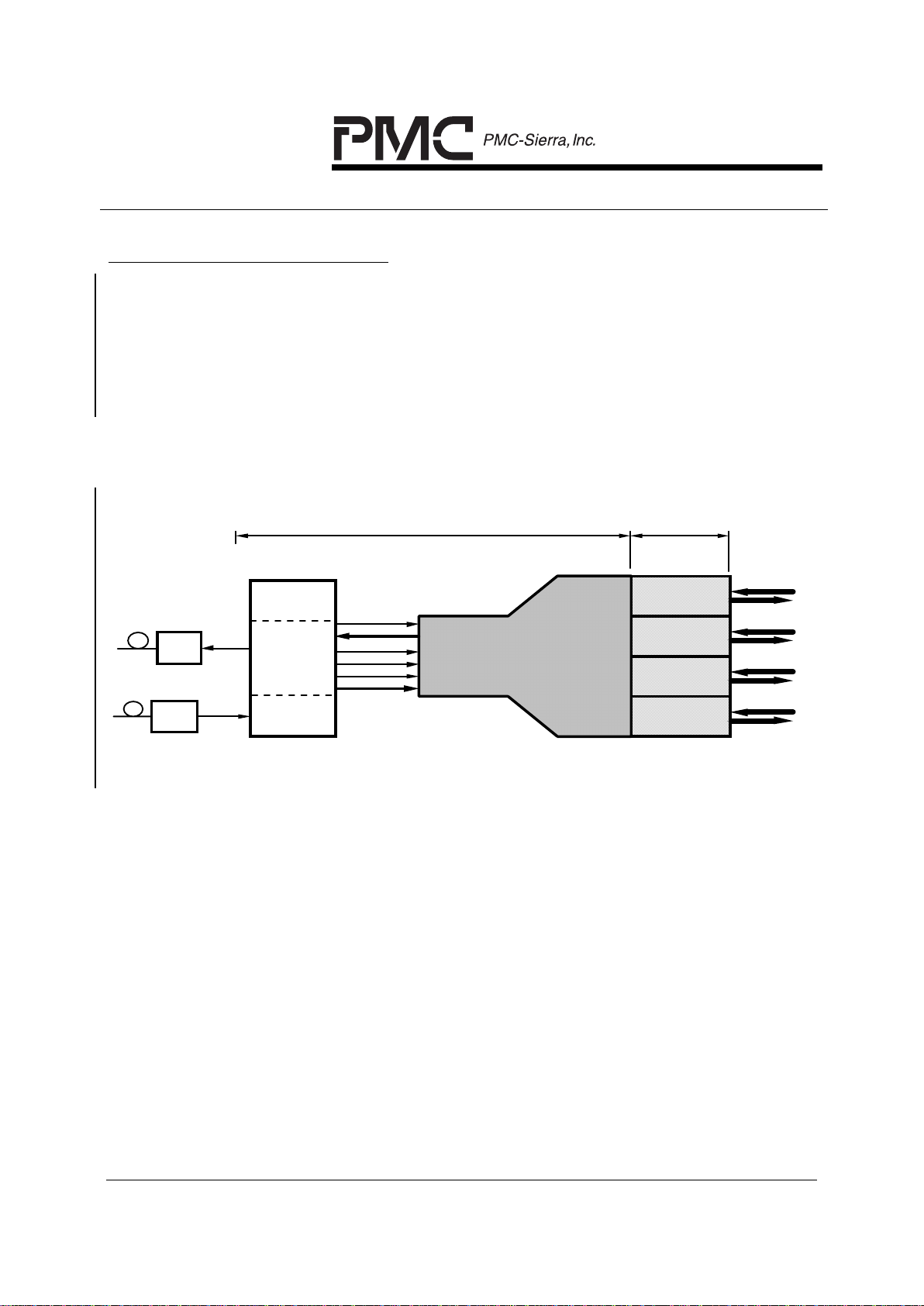
APPLICATION EXAMPLES
The following two diagrams shown the STTX used in an ATM application as an
STS-3c/STM-1 to STS-12/STM-4 multiplexer using four PM5345 SUNI-155 ATM
interface chips, and in an add-drop multiplexer application using four PM5344
SPTX path termination chips instead of the SUNI-155 chips to achieve access to
circuit-switched bandwidth. Ser ial to Parallel / Parallel to Serial conversion, clock
recovery and clock synthesis is available from a number of commercial sources.
Figure 1 - 622 Mbit/s SONET/SDH Asynchronous Transfer Mode
Multiplexer
PM5312
STTX
E/O
O/E
OOF
TOUT[7:0]
TCLK
RICLK
RIFP
RIN[7:0]
PM5345
S/UNI-155
#1
#2
#3
#4
OPTICAL
FACILITY
ATM
SWITCH
CORE
STS-3(STM-1) To STS-12 (STM-4) MUX
STS-3c (STM-1)
ATM Termination
Parallel
to/from
Serial
Conversion
Clock
Synthesis
Clock
Recovery
622 Mbit/s Front End *
* Contact PMC-Sierra Applications regarding
622 Mbit/s Front End alternatives
Page 11
PM5312 STTX
DATA SHEET
PMC-930829 ISSUE 5 SONET/SDH TRANSPORT TERMINATING TRANSCEIVER
PROPRIETARY AND CONFIDENTIALTO PMC-SIERRA, INC., AND FOR ITS CUSTOMERS’ INTERNAL USE
5
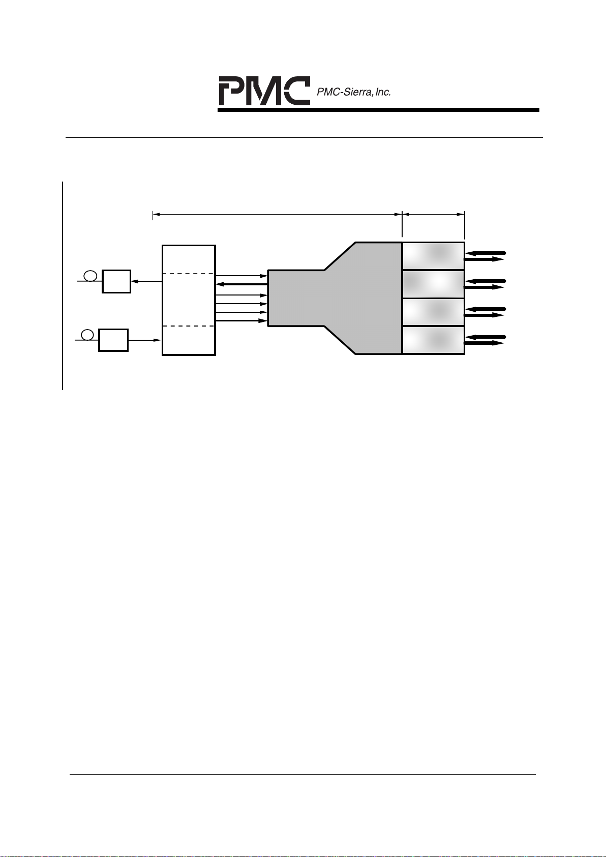
Figure 2 - 622 Mbit/s SONET/SDH Add-Drop Multiplexer Aggregate
Interface
ADD-DROP
MUX
BACKPLANE
PM5312
STTX
E/O
O/E
OOF
TOUT[7:0]
TCLK
RICLK
RIFP
RIN[7:0]
PM5344
SPTX
#1
#2
#3
#4
OPTICAL
FACILITY
STS-3(STM-1) To STS-12 (STM-4) MUX
STS-3c (STM-1)
Path Termination
Parallel
to/from
Serial
Conversion
Clock
Synthesis
Clock
Recovery
622 Mbit/s Front End *
* Contact PMC-Sierra Applications regarding
622 Mbit/s Front End alternatives
Page 12
PM5312 STTX
DATA SHEET
PMC-930829 ISSUE 5 SONET/SDH TRANSPORT TERMINATING TRANSCEIVER
PROPRIETARY AND CONFIDENTIALTO PMC-SIERRA, INC., AND FOR ITS CUSTOMERS’ INTERNAL USE
6
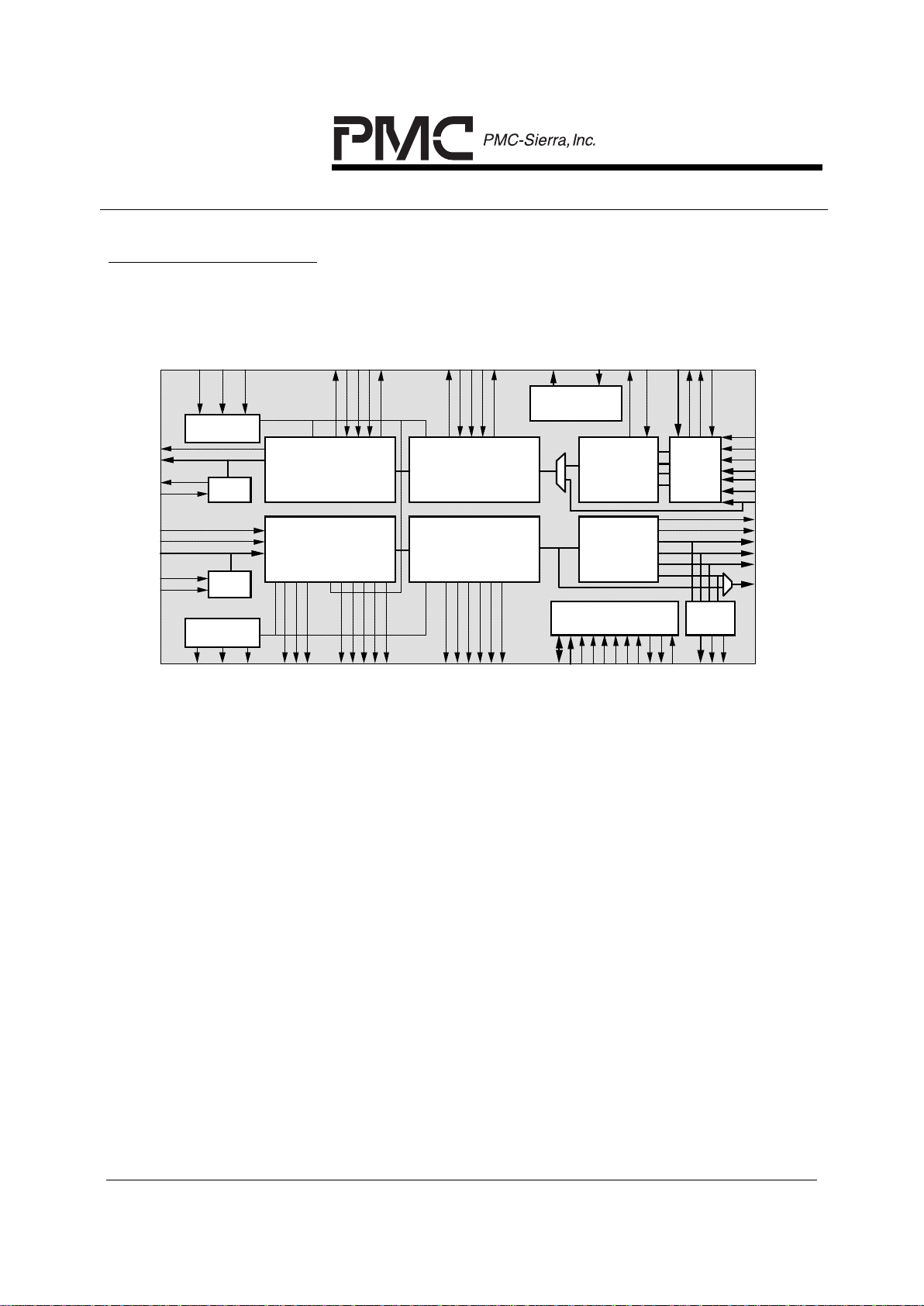
5
BLOCK DIAGRAM
TOUT[7:0]
RIN[7:0]
RICLK
RIFP
Status Control Port
TLAIS/TRCPDA
T
TIN1[7:0]
ROUT1[7:0]
ROCLK
D[7:0]
A[4:0]
ALE
CSB/LCSB
RDB
WRB
RSTB
INTB/LINTB
Microprocessor
I/F
Rx
O/H
Access
Tx
O/H
Access
TTOH[4:1]
RTOH[4:1]
TTOHCLK
RTOHCLK
LOS/RRCPFP
LOF
RTOHFP
TTOHFP
Rx Section
(Regenerator Section)
O/H Processor
Rx Line
(Multiplexer Section)
O/H Processor
TTOHEN
TFERF/TRCPFP
LAIS/RRCPDAT
FERF/RRCPCLK
TICLK
TOFP
OOF
B1E
RLAIS/TRCPCL
K
RSDCLK
RSD
RSOW
RSUC
ROWCLK
B2E
RLDCLK
RLD
RLOW
RAPS
RAPSCLK
ROUT2[7:0]
ROUT3[7:0]
ROUT4[7:0]
ROFP
Byte Interleaved
Multiplex
TIN2[7:0]
TIN3[7:0]
TIN4[7:0]
TIFP
TDIS
Tx Line
(Multiplexer Section)
O/H Processor
Tx Section
(Regenerator Section)
O/H Processor
TCLK
TSDCLK
TSD
TSOW
TSUC
TOWCLK
TLDCLK
TLD
TLOW
TAPS
TAPSCLK
Par/Ser
TSOUT
TSICLK
Ser/Par
RSICLK
RSIN
SCPO[5:0] *
SCPI[3:0] *
GTICLK
A[5]/SCSB
* SINTB
* SLIM
* NOT AVAILABLE WITH
180 CPGA PACKAGING OPTION
Transmit Ring
Control Port
Receive Ring
Control Port
Byte Interleaved
Demultiplex
Page 13

PM5312 STTX
DATA SHEET
PMC-930829 ISSUE 5 SONET/SDH TRANSPORT TERMINATING TRANSCEIVER
PROPRIETARY AND CONFIDENTIALTO PMC-SIERRA, INC., AND FOR ITS CUSTOMERS’ INTERNAL USE
7
6
DESCRIPTION
The PM5312 STTX SONET/SDH Transport Overhead Terminating Transceiver
processes the transport overhead (regenerator and multiplexer section overhead)
of STS-1, STS-3/STM-1, and STS-12/STM-4 streams and optionally provides
byte interleaved multiplexing of lower rate streams.
The STTX may be used on the line side of four PM5344 SPTX SONET/SDH
Path Terminating Transceiver devices to implement a full SONET/SDH path
transmission system capable of terminating 12 STS-1 or four STS-3/STM-1
channels.
In a similar fashion, the STTX may be used on the line side of four PM5345 SUNI
Saturn User Network Interface devices to implement an Asynchronous Transfer
Mode (ATM) Multiplexer which takes four logical ATM streams operating at 155
Mbit/s and synchronously multiplexes them into a single 622 Mbit/s stream.
Page 14

PM5312 STTX
DATA SHEET
PMC-930829 ISSUE 5 SONET/SDH TRANSPORT TERMINATING TRANSCEIVER
PROPRIETARY AND CONFIDENTIALTO PMC-SIERRA, INC., AND FOR ITS CUSTOMERS’ INTERNAL USE
8
7
PIN DIAGRAM
The STTX is available in a 208 pin slugged PQFP package having a body size of
28 mm by 28 mm and a pin pitch of 0.5 mm.
PM5312
STTX
TOP VIEW
TAPSCLK
TLD
TLDCLK
TSD
VDDO
VSSO
TCLK
TSDCLK
TFERF/TRCPFP
TLAIS/TRCPDAT
TSICLK
TSOUT
NC
NC
D[6]
D[7]
INTB/LINTB
VSSO
RDB
WRB
CSB/LCSB
SCPI[1]
TIN1[2]
SCPI[0]
VSSI
VDDI
TIN1[1]
TIN1[0]
TIN2[2]
TIN2[1]
NC
TIN3[7]
TIN3[6]
TIN3[5]
TIN3[4]
TIN3[3]
TIN3[2]
TIN3[1]
TIN3[0]
TIN2[7]
TIN2[6]
TIN2[5]
TIN2[4]
NC
NC
NC
NC
TOFP
VSSO
TOUT[7]
TOUT[6]
TOUT[5]
TOUT[4]
TOUT[3]
TOUT[2]
VSSO
VDDO
TOUT[1]
B1E
NC
TIN4[0]
TIN4[1]
TIN4[2]
TIN4[3]
TIN4[4]
TIN4[5]
VDDI
VSSI
TIN4[6]
TIN4[7]
TTOH[1]
TTOH[2]
TTOH[3]
NC
ROUT2[0]
ROUT1[7]
ROUT1[6]
ROUT1[5]
ROUT1[4]
ROUT1[3]
VDDI
VSSI
ROUT1[2]
ROUT1[1]
VSSO
RTOHFP
NC
TIN2[3]
TIN2[0]
TIN1[7]
TOUT[0]
TTOH[4]
TTOHEN
TTOHFP
TTOHCLK
VDDO
ROUT2[1]
ROUT2[2]
FERF/RRCPCLK
LOS/RRCPFP
LAIS/RRCPDAT
ROUT1[0]
RTOHCLK
TIN1[6]
TIN1[5]
TIN1[4]
TIN1[3]
GTICLK
D[0]
SCPO[0]
D[1]
SCPO[1]
ROUT2[3]
VSSO
RLOW
RSOW
RSUC
ROWCLK
ROUT2[4]
SCPO[2]
ROUT2[5]
SCPO[3]
D[2]
VSSO
SLIM
VDDO
D[3]
SINTB
D[4]
RAPS
ROUT2[6]
VSSO
VDDO
ROUT2[7]
SCPO[4]
ROUT3[0]
SCPO[5]
ROUT3[1]
SCPI[3]
RAPSCLK
SCPI[2]
RLD
RLDCLK
VDDO
B2E
TIFP
TDIS
TLOW
TSOW
TSUC
VDDO
TOWCLK
TAPS
D[5]
NC
LOF
OOF
RIN[7]
RIN[6]
RIN[5]
RIN[4]
RIN[3]
ROUT3[2]
ROUT3[3]
ROUT3[4]
ROUT3[5]
VDDO
ROUT3[6]
ROUT3[7]
ROUT4[0]
TICLK
RSTB
ALE
A[0]
A[1]
A[2]
A[3]
A[4]
A[5]/SCSB
RTOH[1]
RTOH[2]
RTOH[3]
RTOH[4]
ROUT4[1]
ROUT4[2]
ROUT4[3]
VSSO
ROUT4[4]
ROUT4[5]
ROUT4[6]
ROUT4[7]
ROFP
ROCLK
VDDO
RSIN
RIN[2]
RIN[1]
RIN[0]
RIFP
VDDI
VSSI
RLAIS/TRCPCLK
RSD
RSDCLK
RSICLK
RICLK
VSSO
PIN 52
PIN 53
PIN 104
PIN 105
PIN 1
PIN 208
PIN 157
PIN 156
Index
NC
Page 15

PM5312 STTX
DATA SHEET
PMC-930829 ISSUE 5 SONET/SDH TRANSPORT TERMINATING TRANSCEIVER
PROPRIETARY AND CONFIDENTIALTO PMC-SIERRA, INC., AND FOR ITS CUSTOMERS’ INTERNAL USE
9
8
PIN DESCRIPTION
Pin Name Pin
Type
PQFP
Pin
No.
Function
RICLK/ Input 153 The receive incoming clock (RICLK) provides
timing for processing the byte serial receive
stream, RIN[7:0]. RICLK is nominally a 6.48
MHz (STS-1), 19.44 MHz (STS-3/STM-1 ), or
77.76 MHz (STS-12/STM-4) 50% duty cycle
clock, depending on the selected operating
mode. RIN[7:0], and RIFP are sampled on the
rising edge of RICLK.
The receive vector clock (RVCLK) is used
during STTX production test to verify internal
functionality.
RIN[7]
RIN[6]
RIN[5]
RIN[4]
RIN[3]
RIN[2]
RIN[1]
RIN[0]
Input
Input
Input
Input
Input
Input
Input
Input
138
139
140
141
142
143
144
145
The receive incoming stream (RIN[7:0]) carries
the scrambled STS-1, STS-3/STM-1, or STS-
12/STM-4 stream in byte serial format. RIN[7]
is the most significant bit (corresponding to bit 1
of each serial PCM word, the first bit
transmitted). RIN[0] is the least significant bit
(corresponding to bit 8 of each serial PCM
word, the last bit transmitted). RIN[7:0] is
sampled on the rising edge of RICLK.
RIFP Input 146 The active high receive incoming framing
position (RIFP) signal indicates the frame
alignment in the incoming stream, RIN[7:0].
RIFP is sampled on the rising edge of RICLK.
RSICLK/ Input 152 The receive serial incoming clock (RSICLK)
provides timing for processing the bit serial
receive stream, RSIN. RSICLK is nominally a
51.84 MHz, 50% duty cycle clock. RSIN is
sampled on the rising edge of RSICLK.
RSICLK is divided by eight to produce ROCLK
when the bit serial STS-1 mode is selected.
RSICLK should be disabled when the bit serial
STS-1 interface is not used.
RSIN Input 158 The receive incoming serial stream (RSIN)
carries the scrambled STS-1 stream in bit serial
format. RSIN is sampled on the rising edge of
RSICLK.
Page 16

PM5312 STTX
DATA SHEET
PMC-930829 ISSUE 5 SONET/SDH TRANSPORT TERMINATING TRANSCEIVER
PROPRIETARY AND CONFIDENTIALTO PMC-SIERRA, INC., AND FOR ITS CUSTOMERS’ INTERNAL USE
10
Pin Name Pin
Type
PQFP
Pin
No.
Function
RLAIS/ Input 149 The receive line AIS insertion (RLAIS) signal
controls the insertion of line AIS in the receive
outgoing streams, ROUT1[7:0], ROUT2[7:0],
ROUT3[7:0], and ROUT4[7:0] when the ring
control port is disabled. When RLAIS is high,
line AIS is inserted in the outgoing streams.
Line AIS is also optionally inserted
automatically upon detection of loss of signal,
loss of frame, or line AIS in the incoming
stream. RLAIS is sampled on the rising edge of
RICLK.
TRCPCLK The transmit ring control port clock (TRCPCLK)
signal provides timing for the transmit ring
control port when the ring control port is
enabled (the enabling and disabling of the ring
control port is controlled by a bit in the Master
Control Register). TRCPCLK is nomina lly a
3.24 MHz, 50% duty cycle clock and is normally
connected to the RRCPCLK output of a mate
STTX in ring-based add-drop multiplexer
applications. TRCPFP and TRCPDAT are
sampled on the rising edge of TRCPCLK.
OOF Output 137 The out of frame (OOF) signal is set high while
the STTX is unable to find a valid framing
pattern (A1, A2) in the incoming stream. OOF is
set low when a valid framing pattern is detected.
OOF is updated on the rising edge of RICLK.
LOF Output 136 The loss of frame (LOF) signal is set high when
an out of frame state persists for 3 ms. LOF is
set low when an in frame state persists for 3 ms.
LOF is updated on the rising edge of RICLK.
Page 17

PM5312 STTX
DATA SHEET
PMC-930829 ISSUE 5 SONET/SDH TRANSPORT TERMINATING TRANSCEIVER
PROPRIETARY AND CONFIDENTIALTO PMC-SIERRA, INC., AND FOR ITS CUSTOMERS’ INTERNAL USE
11
Pin Name Pin
Type
PQFP
Pin
No.
Function
LOS/ Output 120 Loss of signal (LOS) is active when the ring
control port is disabled. Loss of signal (LOS) is
set high when a violating period (20 ± 2.5 µs) of
consecutive all zeros patterns is detected in the
incoming stream. LOS is set low when two valid
framing words (A1, A2) are detected, and during
the intervening time (125 µs), no violating
period of all zeros patterns is observed. LOS is
updated on the rising edge of RICLK.
RRCPFP The receive ring control port frame position
(RRCPFP) signal identifies bit positions in the
receive ring control port data (RRCPDAT) when
the ring control port is enabled (the enabling
and disabling of the ring control port is
controlled by a bit in the Master Control
Register). RRCPFP is high during the filtered
K1, K2 bit positions, the change of APS value
bit position, the protection switch byte failure bit
position, and the send AIS and send FERF bit
positions in the RRCPDAT stream. RRCPFP is
normally connected to the TRCPFP input of a
mate STTX in ring-based add-drop multiplexer
applications. RRCPFP is updated on the falling
edge of RRCPCLK.
B1E Output 135 The B1 error clock (B1E) is a return to zero
signal that pulses once for every section bit
interleaved parity error (B1) detected in the
incoming stream. Up to eight pulses may occur
on B1E per frame.
Page 18

PM5312 STTX
DATA SHEET
PMC-930829 ISSUE 5 SONET/SDH TRANSPORT TERMINATING TRANSCEIVER
PROPRIETARY AND CONFIDENTIALTO PMC-SIERRA, INC., AND FOR ITS CUSTOMERS’ INTERNAL USE
12
Pin Name Pin
Type
PQFP
Pin
No.
Function
FERF/ Output 119 The far end receive failure (FERF) signal is
active when the ring control port is disabled.
FERF is set high when line FERF is detected in
the incoming stream. FERF is declared when a
110 binary pattern is detected in bits 6, 7, and 8
of the K2 byte for three or five consecutive
frames. FERF is removed when any pattern
other than 110 is detected in bits 6, 7, and 8 of
the K2 byte for three or five consecutive frames.
This alarm indication is also available through
register access. FERF is updated on the rising
edge of RICLK.
RRCPCLK The receive ring control port clock (RRCPCLK)
signal provides timing for the receive ring
control port when the ring control port is
enabled (the enabling and disabling of the ring
control port is controlled by a bit in the Master
Control Register). RRCPCLK is nominally a
3.24 MHz, 50% duty cycle clock and is normally
connected to the TRCPCLK input of a mate
STTX in ring-based add-drop multiplexer
applications. RRCPFP and RRCPDAT are
updated on the falling edge of RRCPCLK.
Page 19

PM5312 STTX
DATA SHEET
PMC-930829 ISSUE 5 SONET/SDH TRANSPORT TERMINATING TRANSCEIVER
PROPRIETARY AND CONFIDENTIALTO PMC-SIERRA, INC., AND FOR ITS CUSTOMERS’ INTERNAL USE
13
Pin Name Pin
Type
PQFP
Pin
No.
Function
LAIS/ Output 121 The line alarm indication (LAIS) signal is active
when the ring control port is disabled. LAIS is
set high when line AIS is detected in the
incoming stream. LAIS is declared when a 111
binary pattern is detected in bits 6, 7, and 8 of
the K2 byte for three or five consecutive frames.
LAIS is removed when any pattern other than
111 is detected in bits 6, 7, and 8 of the K2 byte
for three or five consecutive frames. This alarm
indication is also available through register
access. LAIS is updated on the rising edge of
RICLK.
RRCPDAT The receive ring control port data (RRCPDAT)
signal contains the receive ring control port data
stream when the ring control port is enabled
(the enabling and disabling of the ring control
port is controlled by a bit in the Master Control
Register). The receive ring control port data
consists of the filtered K1, K2 byte values, the
change of APS value bit position, the protection
switch byte failure status bit position, the send
AIS and send FERF bit positions, and the line
FEBE bit positions. RRCPDAT is normally
connected to the TRCPDAT input of a mate
STTX in ring-based add-drop multiplexer
applications. RRCPDAT is updated on the
falling edge of RRCPCLK.
B2E Output 134 The B2 error clock (B2E) is a return to zero
signal that pulses once for every line bit
interleaved parity error (B2) detected in the
incoming stream. Up to 8 (STS-1), 24 (STS-
3/STM-1), or 96 (STS-12/STM-4) pulses may
occur on B2E, per frame.
RSDCLK Output 151 The receive section DCC clock (RSDCLK) is a
192 kHz clock used to update the RSD output.
RSDCLK is generated by gapping a 216 kHz
clock.
Page 20

PM5312 STTX
DATA SHEET
PMC-930829 ISSUE 5 SONET/SDH TRANSPORT TERMINATING TRANSCEIVER
PROPRIETARY AND CONFIDENTIALTO PMC-SIERRA, INC., AND FOR ITS CUSTOMERS’ INTERNAL USE
14
Pin Name Pin
Type
PQFP
Pin
No.
Function
RSD Output 150 The receive section DCC (RSD) signal contains
the section data communications channel (D1,
D2, D3) extracted from the incoming stream.
RSD is updated on the falling edge of RSDCLK.
ROWCLK Output 126 The receive order wire clock (ROWCLK) is a 64
kHz clock used to update the RSOW, RSUC,
and RLOW outputs. ROWCLK is generated by
gapping a 72 kHz clock.
RSOW Output 124 The receive section order wire (RSOW) signal
contains the section order wire channel (E1)
extracted from the incoming stream. RSOW is
updated on the falling edge of ROWCLK.
RSUC Output 125 The receive section user channel (RSUC) signal
contains the section user channel (F1) extracted
from the incoming stream. RSUC is updated on
the falling edge of ROWCLK.
RLOW Output 123 The receive line order wire (RLOW) signal
contains the line order wire channel (E2)
extracted from the incoming stream. RLOW is
updated on the falling edge of ROWCLK.
RLDCLK Output 1 32 The receive line DCC clock (RLDCLK) is a 576
kHz clock used to update the RLD output.
RLDCLK is generated by gapping a 2.16 MHz
clock.
RLD Output 131 The receive line DCC (RLD) signal contains the
line data communications channel (D4 - D12)
extracted from the incoming stream. RLD is
updated on the falling edge of RLDCLK.
RAPSCLK Output 129 The receive automatic protection switch channel
clock (RAPSCLK) is a 128 kHz clock used to
update the RAPS output. RAPSCLK is
generated by gapping a 144 kHz clock.
RAPS Output 127 The receive automatic protection switch channel
(RAPS) signal carries the automatic protection
switch channel (K1, K2) extracted from the
incoming stream. RAPS is updated on the
falling edge of RAPSCLK.
Page 21

PM5312 STTX
DATA SHEET
PMC-930829 ISSUE 5 SONET/SDH TRANSPORT TERMINATING TRANSCEIVER
PROPRIETARY AND CONFIDENTIALTO PMC-SIERRA, INC., AND FOR ITS CUSTOMERS’ INTERNAL USE
15
Pin Name Pin
Type
PQFP
Pin
No.
Function
RTOH[4]
RTOH[3]
RTOH[2]
RTOH[1]
Output
Output
Output
Output
2
3
4
5
The receive transport overhead bus
(RTOH[4:1]) contains the receive transport
overhead bytes (A1, A2, C1, B1, E1, F1, D1-D3,
H1-H3, B2, K1, K2, D4-D12, Z1, Z2, and E2)
extracted from the incoming stream. When
STS-12/STM-4 mode is selected, RTOH[1]
contains the transport overhead from STS-
3/STM-1 #1, RTOH[2] contains the transport
overhead for
STS-3/STM-1 #2, RTOH[3] contains the
transport overhead for STS-3/STM-1 #3, and
RTOH[4] contains the transport overhead for
STS-3/STM-1 #4. When STS-3/STM-1 mode or
STS-1 mode are selected, the complete
transport overhead is extracted on RTOH[1].
RTOH[4:1] is updated on the falling edge of
RTOHCLK.
RTOHCLK Output 205 The receive transport overhead clock
(RTOHCLK) is nominally a 5.184 MHz clock that
provides timing to process the extracted receive
transport overhead bus, RTOH[4:1]. RTOHCLK
is a gapped 6.48 MHz clock when accessing the
transport overhead of STS-3/STM-1 streams.
RTOHCLK is a gapped 2.16 MHz clock when
accessing the transport overhead of an STS-1
stream.
RTOHFP Output 207 The receive transport overhead frame position
(RTOHFP) signal is used to locate the individual
receive transport overhead bits in the transport
overhead bus, RTOH[4:1]. RTOHFP is set high
while bit 1 (the most significant bit) of the first
framing byte (A1) is present in the RTOH[4:1]
stream. RTOHFP is updated on the falling edge
of RTOHCLK.
Page 22

PM5312 STTX
DATA SHEET
PMC-930829 ISSUE 5 SONET/SDH TRANSPORT TERMINATING TRANSCEIVER
PROPRIETARY AND CONFIDENTIALTO PMC-SIERRA, INC., AND FOR ITS CUSTOMERS’ INTERNAL USE
16
Pin Name Pin
Type
PQFP
Pin
No.
Function
ROCLK Output 160 The receive outgoing clock (ROCLK) provides
timing for updating the demultiplexed byte serial
STS-1 or STS-3/STM-1 outputs, ROUT1[7:0],
ROUT2[7:0], ROUT3[7:0], and ROUT4[7:0]
when 1:3 or 1:4 byte interleaved multiplexing is
enabled. ROCLK is nominally a 6.48 MHz, or
19.44 MHz clock, depending on the
demultiplexing mode selected. ROCLK remains
inactive when demultiplexing is bypassed.
When the bit serial STS-1 receive interface is
enabled, ROCLK becomes the generated byte
serial clock. ROCLK is a 6.48 MHz clock that is
generated by dividing the receive serial
incoming clock (RSICLK) by eight. ROCLK
must be connected externally to the receive
incoming clock (RICLK) when processing a bit
serial
STS-1 stream.
ROUT1[7]
ROUT1[6]
ROUT1[5]
ROUT1[4]
ROUT1[3]
ROUT1[2]
ROUT1[1]
ROUT1[0]
Output
Output
Output
Output
Output
Output
Output
Output
195
196
197
198
199
202
203
204
The receive outgoing #1 bus, (ROUT1[7:0]),
carries demultiplexed STS-1 or STS-3/STM-1
streams in byte serial format. ROUT1[7] is the
most significant bit (corresponding to bit 1 of
each serial PCM word, the first bit received).
ROUT1[0] is the least significant bit
(corresponding to bit 8 of each serial PCM
word). ROUT1[7:0] is updated on the falling
edge of ROCLK.
ROUT1[7:0] contains the entire descrambled
outgoing stream and is updated on the rising
edge of RICLK when demultiplexing is
bypassed, or when the bit serial STS-1 mode is
selected. Note that demultiplex bypass is
supported for STS-3 mode only.
Page 23

PM5312 STTX
DATA SHEET
PMC-930829 ISSUE 5 SONET/SDH TRANSPORT TERMINATING TRANSCEIVER
PROPRIETARY AND CONFIDENTIALTO PMC-SIERRA, INC., AND FOR ITS CUSTOMERS’ INTERNAL USE
17
Pin Name Pin
Type
PQFP
Pin
No.
Function
ROUT2[7]
ROUT2[6]
ROUT2[5]
ROUT2[4]
ROUT2[3]
ROUT2[2]
ROUT2[1]
ROUT2[0]
Output
Output
Output
Output
Output
Output
Output
Output
182
185
187
189
190
191
192
194
The receive outgoing #2 bus, (ROUT2[7:0]),
carries demultiplexed STS-1 or STS-3/STM-1
streams in byte serial format. ROUT2[7] is the
most significant bit (corresponding to bit 1 of
each serial PCM word, the first bit received).
ROUT2[0] is the least significant bit
(corresponding to bit 8 of each serial PCM
word). ROUT2[7:0] is updated on the falling
edge of ROCLK.
ROUT3[7]
ROUT3[6]
ROUT3[5]
ROUT3[4]
ROUT3[3]
ROUT3[2]
ROUT3[1]
ROUT3[0]
Output
Output
Output
Output
Output
Output
Output
Output
171
172
174
175
176
177
178
180
The receive outgoing #3 bus, (ROUT3[7:0]),
carries demultiplexed STS-1 or STS-3/STM-1
streams in byte serial format. ROUT3[7] is the
most significant bit (corresponding to bit 1 of
each serial PCM word, the first bit transmitted).
ROUT3[0] is the least significant bit
(corresponding to bit 8 of each serial PCM
word). ROUT3[7:0] is updated on the falling
edge of ROCLK.
ROUT4[7]
ROUT4[6]
ROUT4[5]
ROUT4[4]
ROUT4[3]
ROUT4[2]
ROUT4[1]
ROUT4[0]
Output
Output
Output
Output
Output
Output
Output
Output
162
163
164
165
167
168
169
170
The receive outgoing #4 bus, (ROUT4[7:0]),
carries demultiplexed STS-3/STM-1 streams in
byte serial format. ROUT4[7] is the most
significant bit (corresponding to bit 1 of each
serial PCM word, the first bit transmitted).
ROUT4[0] is the least significant bit
(corresponding to bit 8 of each serial PCM
word). ROUT4[7:0] is updated on the falling
edge of ROCLK. ROUT4[7:0] is not used when
demultiplexing an STS-3 stream into three STS-
1 streams.
Page 24

PM5312 STTX
DATA SHEET
PMC-930829 ISSUE 5 SONET/SDH TRANSPORT TERMINATING TRANSCEIVER
PROPRIETARY AND CONFIDENTIALTO PMC-SIERRA, INC., AND FOR ITS CUSTOMERS’ INTERNAL USE
18
Pin Name Pin
Type
PQFP
Pin
No.
Function
ROFP Output 161 The active high receive outgoing frame position
(ROFP) signal is set high once per frame in the
byte position immediately following the C1 bytes
in the ROUT1[7:0], ROUT2[7:0], ROUT3[7:0],
and ROUT4[7:0] STS-1 or STS-3/STM-1
streams. ROFP is updated on the falling edge
of ROCLK.
ROFP is also used to mark the alignment of the
RSOW, RSUC, RLOW and RAPS bit streams.
ROFP is updated on the rising edge of RICLK
when demultiplexing is bypassed, or when the
bit serial STS-1 mode is selected. Note that
demultiplex bypass is supported for STS-3
mode only.
TCLK/ Input 97 The transmit clock (TCLK) provides timing for
multiplexing the byte serial incoming streams,
TIN1[7:0], TIN2[7:0], TIN3[7:0] and TIN4[7:0],
into a higher rate stream. TCLK is nominally a
6.48 MHz, 19.44 MHz or 77.76 MHz 50% duty
cycle clock, depending on the operating mode
selected. When multiplexing is bypassed, or
when STS-1 mode is selected, the incoming
stream, TIN1[7:0], is sampled on the rising edge
of TCLK.
TVCLK The transmit vector clock (TVCLK) is used
during STTX production test to verify internal
functionality.
Page 25

PM5312 STTX
DATA SHEET
PMC-930829 ISSUE 5 SONET/SDH TRANSPORT TERMINATING TRANSCEIVER
PROPRIETARY AND CONFIDENTIALTO PMC-SIERRA, INC., AND FOR ITS CUSTOMERS’ INTERNAL USE
19
Pin Name Pin
Type
PQFP
Pin
No.
Function
GTICLK Output 34 The generated transmit clock (GTICLK) is used
in contra-directional timing-based systems to
provide timing for upstream circuitry. GTICLK is
a divide by four of the high speed multiplex
clock (TCLK) when STS-3 to STS-12
multiplexing is enabled. GTICLK is a divide by
three of TCLK when STS-1 to STS-3
multiplexing is enabled. GTICLK must be
connected directly to
TICLK for these contra-directional multiplexing
applications. GTICLK is a divide by eight of the
transmit serial incoming clock (TSICLK) when
the bit serial STS-1 mode is enabled. GTICLK
must be connected directly to TCLK for these
contra-directional STS-1 applications.
TICLK Input 14 The transmit incoming clock (TICLK) provides
timing to sample the byte serial incoming
streams prior to multiplexing. TICLK is
synchronous with, but arbitrarily phase aligned
to TCLK. TICLK is nominally a 6.48 MHz, or
19.44 MHz clock. TIN1[7:0], TIN2[7:0],
TIN3[7:0], TIN4[7:0], TDIS, and TIFP are
sampled on the rising edge of TICLK.
TSICLK Input 101 The transmit serial incoming clock (TSICLK)
provides timing for updating the bit serial
outgoing stream when STS-1 mode is selected.
TSICLK is nominally a 51.84 MHz, 50% duty
cycle clock. TSOUT is updated on the rising
edge of TSICLK. TSICLK should be disabled
when the bit serial STS-1 interface is not used.
Page 26

PM5312 STTX
DATA SHEET
PMC-930829 ISSUE 5 SONET/SDH TRANSPORT TERMINATING TRANSCEIVER
PROPRIETARY AND CONFIDENTIALTO PMC-SIERRA, INC., AND FOR ITS CUSTOMERS’ INTERNAL USE
20
Pin Name Pin
Type
PQFP
Pin
No.
Function
TIN1[7]
TIN1[6]
TIN1[5]
TIN1[4]
TIN1[3]
TIN1[2]
TIN1[1]
TIN1[0]
Input 71
72
73
74
75
77
81
82
The transmit incoming #1 bus, (TIN1[7:0]),
carries STS-1 or STS-3/STM-1 streams in byte
serial format. TIN1[7] is the most significant bit
(corresponding to bit 1 of each serial PCM
word, the first bit transmitted). TIN1[0] is the
least significant bit (corresponding to bit 8 of
each serial PCM word). TIN1[7:0] is sampled on
the rising edge of TICLK.
TIN1[7:0] contains the entire incoming stream
and is sampled on the rising edge of TCLK
when multiplexing is bypassed, or when the
STS-1 mode is selected. Note that multiplex
bypass is supported for STS-3 mode only.
TIN2[7]
TIN2[6]
TIN2[5]
TIN2[4]
TIN2[3]
TIN2[2]
TIN2[1]
TIN2[0]
Input 63
64
65
66
67
68
69
70
The transmit incoming #2 bus, (TIN2[7:0]),
carries STS-1 or STS-3/STM-1 streams in byte
serial format. TIN2[7] is the most significant bit
(corresponding to bit 1 of each serial PCM
word, the first bit transmitted). TIN2[0] is the
least significant bit (corresponding to bit 8 of
each serial PCM word). TIN2[7:0] is sampled on
the rising edge of TICLK.
TIN3[7]
TIN3[6]
TIN3[5]
TIN3[4]
TIN3[3]
TIN3[2]
TIN3[1]
TIN3[0]
Input 55
56
57
58
59
60
61
62
The transmit incoming #3 bus, (TIN3[7:0]),
carries STS-1 or STS-3/STM-1 streams in byte
serial format. TIN3[7] is the most significant bit
(corresponding to bit 1 of each serial PCM
word, the first bit transmitted). TIN3[0] is the
least significant bit (corresponding to bit 8 of
each serial PCM word). TIN3[7:0] is sampled on
the rising edge of TICLK.
TIN4[7]
TIN4[6]
TIN4[5]
TIN4[4]
TIN4[3]
TIN4[2]
TIN4[1]
TIN4[0]
Input 42
43
46
47
48
49
50
51
The transmit incoming #4 bus, (TIN3[7:0]),
carries STS-3/STM-1 streams in byte serial
format. TIN4[7] is the most significant bit
(corresponding to bit 1 of each serial PCM
word, the first bit transmitted). TIN4[0] is the
least significant bit (corresponding to bit 8 of
each serial PCM word). TIN4[7:0] is sampled on
the rising edge of TICLK. TIN4[7:0] is not used
when multiplexing three STS-1 streams to an
STS-3 stream.
Page 27

PM5312 STTX
DATA SHEET
PMC-930829 ISSUE 5 SONET/SDH TRANSPORT TERMINATING TRANSCEIVER
PROPRIETARY AND CONFIDENTIALTO PMC-SIERRA, INC., AND FOR ITS CUSTOMERS’ INTERNAL USE
21
Pin Name Pin
Type
PQFP
Pin
No.
Function
TIFP Input 83 The active high transmit incoming framing
position (TIFP) signal indicates the frame
alignment for incoming streams. A high level on
TIFP marks the byte immediately following the
C1 bytes in the transmit STS-1 or STS-3 (STM-
1) streams, TIN1[7:0], TIN2[7:0], TIN3[7:0], and
TIN4[7:0]. TIFP is sampled on the rising edge
of TICLK.
TIFP is sampled on the rising edge of TCLK
when multiplexing is bypassed, or when the bit
serial STS-1 mode is selected. Note that
multiplex bypass is supported for STS-3 mode
only.
TDIS Input 84 The active high transmit disable (TDIS) signal
selectively disables overwriting each of the
STS-1 or STS-3 (STM-1) streams with the
corresponding overhead byte. TDIS is sampled
on the rising edge of TICLK.
TDIS is sampled on the rising edge of TCLK
when multiplexing is bypassed, or when the bit
serial STS-1 mode is selected. Note that TDIS
takes precedence over the values shifted in on
the transmit transport overhead interface
(TTOH[4:1]) using TTOHEN.
In general, the value on TIN[7:0] passes through
transparently if TDIS is high. Three exceptions
exist:
1) Bits 6 to 8 of the K2 byte may be overwritten
by an active FERF indication ("110") regardless
of the state of TDIS.
2) If TDIS is high during the section BIP byte
(B1), the TIN[7:0] value becomes an error mask
for the generated section BIP.
3) If TDIS is high during the line BIP bytes (B2),
the TIN[7:0] value becomes an error mask for
the generated line BIP.
Page 28

PM5312 STTX
DATA SHEET
PMC-930829 ISSUE 5 SONET/SDH TRANSPORT TERMINATING TRANSCEIVER
PROPRIETARY AND CONFIDENTIALTO PMC-SIERRA, INC., AND FOR ITS CUSTOMERS’ INTERNAL USE
22
Pin Name Pin
Type
PQFP
Pin
No.
Function
TTOH[4]
TTOH[3]
TTOH[2]
TTOH[1]
Input 38
39
40
41
The transmit transport overhead bus (TTOH[4:1)
contains the transport overhead bytes (A1, A2,
C1, E1, F1, D1-D3, H3, K1, K2, D4-D12, Z1, Z2,
and E2) and error masks (H1, H2, B1, and B2)
which may be inserted, or used to insert bit
interleaved parity errors or payload pointer bit
errors into the overhead byte positions in the
outgoing stream. Insertion is controlled by the
TTOHEN input. When STS-12/STM-4 mode is
enabled, TTOH[1] contains the transport
overhead for STS-3/STM-1 #1. TTOH[2]
contains the transport overhead for STS-3/STM-
1 #2. TTOH[3] contains the transport overhead
for STS-3/STM-1 #3. TTOH[4] contains the
transport overhead for STS-3/STM-1 #4. When
STS-3/STM-1 mode or STS-1 mode are
selected, TTOH[1] contains the transport
overhead for the entire stream. TTOH[4:1] is
sampled on the rising edge of TTOHCLK.
TTOHFP Output 36 The transmit transport overhead frame position
(TTOHFP) signal is used to locate the individual
transport overhead bits in the transport
overhead bus, TTOH[4:1]. TTOHFP is set high
while bit 1 (the most significant bit) of the first
framing byte (A1) is expected in the incoming
stream. TTOHFP is also used to mark the
alignment of the TSUC, TSOW, TLOW, and
TAPS bit streams. TTOHFP is updated on the
falling edge of TTOHCLK.
TTOHCLK Output 35 The transmit transport overhead clock
(TTOHCLK) is nominally a 5.184 MHz (1.728
MHz for STS-1) clock that provides timing for
upstream circuitry that sources the transport
overhead bus, TTOH[4:1]. TTOHCLK is a
gapped 6.48 MHz clock when accessing the
transport overhead of STS-3/STM-1 streams.
TTOHCLK is a gapped 2.16 MHz clock when
accessing the transport overhead of an STS-1
stream.
Page 29

PM5312 STTX
DATA SHEET
PMC-930829 ISSUE 5 SONET/SDH TRANSPORT TERMINATING TRANSCEIVER
PROPRIETARY AND CONFIDENTIALTO PMC-SIERRA, INC., AND FOR ITS CUSTOMERS’ INTERNAL USE
23
Pin Name Pin
Type
PQFP
Pin
No.
Function
TTOHEN Input 37 The transmit transport overhead insert enable
(TTOHEN) signal controls the source of the
transport overhead data which is inserted in the
TOUT[7:0] stream. While TTOHEN is high (and
TDIS is low), values sampled on the TTOH input
are inserted into the corresponding transport
overhead bit position (for the A1, A2, C1, E1,
F1, D1-D3, H3, K1, K2, D4-D12, Z1, Z2, and E2
bytes). While TTOHEN is low, the default values
are inserted into these transport overhead bit
positions. A high level on TTOHEN during the
H1, H2, B1, or B2 bit positions enables an error
mask. While the error mask is enabled, a high
level on inputs TTOH[4:1] causes the
corresponding H1, H2, B1 or B2 bit positions to
be inverted. A low level on TTOH allows the
corresponding bit positions to pass through the
STTX uncorrupted. TTOHEN is sampled on the
rising edge of TTOHCLK.
Page 30

PM5312 STTX
DATA SHEET
PMC-930829 ISSUE 5 SONET/SDH TRANSPORT TERMINATING TRANSCEIVER
PROPRIETARY AND CONFIDENTIALTO PMC-SIERRA, INC., AND FOR ITS CUSTOMERS’ INTERNAL USE
24
Pin Name Pin
Type
PQFP
Pin
No.
Function
TFERF/ Input 99 The active high transmit far end receive failure
(TFERF) signal controls the insertion of a far
end receive fa ilure indication in the outgoing
stream when the ring control port is disabled.
When TFERF is set high, bits 6, 7, and 8 of the
K2 byte are set to the pattern 110. Line FERF
may also be inserted using the FERF bit in the
TLOP Control Register, or upon detection of
loss of signal, loss of frame, or line AIS in the
receive stream, using the AUTOFERF bit in the
Master Control/Enable Register. TFERF is
sampled on the rising edge of TCLK.
TRCPFP The transmit ring control port frame position
(TRCPFP) signal identifies bit positions in the
transmit ring control port data (TRCPDAT) when
the ring control port is enabled (the enabling
and disabling of the ring control port is
controlled by a bit in the Master Control
Register). TRCPFP is high during the filtered
K1, K2 bit positions, the change of APS value
bit position, the protection switch byte failure bit
position, and the send AIS and send FERF bit
positions in the TRCPDAT stream. TRCPFP is
normally connected to the RRCPFP output of a
mate STTX in ring-based add-drop multiplexer
applications. TRCPFP is sampled on the rising
edge of TRCPCLK.
Page 31

PM5312 STTX
DATA SHEET
PMC-930829 ISSUE 5 SONET/SDH TRANSPORT TERMINATING TRANSCEIVER
PROPRIETARY AND CONFIDENTIALTO PMC-SIERRA, INC., AND FOR ITS CUSTOMERS’ INTERNAL USE
25
Pin Name Pin
Type
PQFP
Pin
No.
Function
TLAIS/ Input 100 The active high transmit line alarm indication
signal (TLAIS) controls the insertion of line AIS
in the outgoing stream when the ring control
port is disabled. When TLAIS is set high, the
complete frame (except the section overhead or
regenerator section) is overwritten with the all
ones pattern (before scrambling). TLAIS is
sampled on the rising edge of TCLK.
TRCPDAT The transmit ring control port data (TRCPDAT)
signal contains the transmit ring control port
data stream when the ring control port is
enabled (the enabling and disabling of the ring
control port is controlled by a bit in the Master
Control Register). The transmit ring control port
data consists of the filtered K1, K2 byte values,
the change of APS value bit position, the
protection switch byte failure status bit position,
the send AIS and send FERF bit positions, and
the line FEBE bit positions. TRCPDAT is
normally connected to the RRCPDAT output of
a mate STTX in ring-based add-drop multiplexer
applications. TRCPDAT is sampled on the rising
edge of TRCPCLK.
TSDCLK Output 98 The transmit section DCC clock (TSDCLK) is a
192 kHz clock used to sample the TSD input.
TSDCLK is generated by gapping a 216 kHz
clock.
TSD Input 94 The transmit section DCC (TSD) signal contains
the section data communications channel (D1,
D2, D3) inserted into the outgoing stream. TSD
is sampled on the rising edge of TSDCLK.
TOWCLK Output 89 The transmit order wire clock (TOWCLK) is a 64
kHz clock used to sample the TSOW, TSUC,
and TLOW inputs. TOWCLK is generated by
gapping a 72 kHz clock.
TSOW Input 86 The transmit section order wire (TSOW) signal
contains the section order wire channel (E1)
inserted into the outgoing stream. TSOW is
sampled on the rising edge of TOWCLK.
Page 32

PM5312 STTX
DATA SHEET
PMC-930829 ISSUE 5 SONET/SDH TRANSPORT TERMINATING TRANSCEIVER
PROPRIETARY AND CONFIDENTIALTO PMC-SIERRA, INC., AND FOR ITS CUSTOMERS’ INTERNAL USE
26
Pin Name Pin
Type
PQFP
Pin
No.
Function
TSUC Input 87 The transmit section user channel (TSUC)
signal contains the section user channel (F1)
inserted into the outgoing stream. TSUC is
sampled on the rising edge of TOWCLK.
TLOW Input 85 The transmit line order wire (TLOW) signal
contains the line order wire channel (E2)
inserted into the outgoing stream. TLOW is
updated on the rising edge of TOWCLK.
TLDCLK Output 93 The transmit line DCC clock (TLDCLK) is a 576
kHz clock used to sample the TLD input.
TLDCLK is generated by gapping a 2.16 MHz
clock.
TLD Input 92 The transmit line DCC (TLD) signal contains the
line data communications channel (D4 - D12)
inserted into the outgoing stream. TLD is
sampled on the rising edge of TLDCLK.
TAPSCLK Output 91 The transmit automatic protection switch
channel clock (TAPSCLK) is a 128 kHz clock
used to sample the TAPS input. TAPSCLK is
generated by gapping a 144 kHz clock.
TAPS Input 90 The transmit automatic protection switch
channel (TAPS) signal carries the automatic
protection switch channel (K1, K2) inserted into
the outgoing stream. TAPS is sampled on the
rising edge of TAPSCLK.
TOUT[7]
TOUT[6]
TOUT[5]
TOUT[4]
TOUT[3]
TOUT[2]
TOUT[1]
TOUT[0]
Output 109
110
111
112
113
114
117
118
The transmit outgoing stream, (TOUT[7:0]),
carries the scrambled STS-1, STS-3/STM-1, or
STS-12/STM-4 stream in byte serial format.
TOUT[7] is the most significant bit
(corresponding to bit 1 of each serial PCM
word, the first bit transmitted). TO UT[0] is the
least significant bit (corresponding to bit 8 of
each serial PCM word). TOUT[7:0] is updated
on the rising edge of TCLK.
TSOUT Output 102 The transmit serial outgoing stream, (TSOUT),
carries the scrambled stream in bit serial format
when STS-1 mode is selected. TSOUT is
updated on the rising edge of TSICLK.
Page 33

PM5312 STTX
DATA SHEET
PMC-930829 ISSUE 5 SONET/SDH TRANSPORT TERMINATING TRANSCEIVER
PROPRIETARY AND CONFIDENTIALTO PMC-SIERRA, INC., AND FOR ITS CUSTOMERS’ INTERNAL USE
27
Pin Name Pin
Type
PQFP
Pin
No.
Function
TOFP Output 107 The active high transmit outgoing frame position
(TOFP) signal is asserted once per frame in the
byte position immediately following the C1 bytes
in the outgoing stream. TOFP is updated on the
rising edge of TCLK.
SCPO[5]
SCPO[4]
SCPO[3]
SCPO[2]
SCPO[1]
SCPO[0]
Output
Output
Output
Output
Output
Output
179
181
186
188
30
32
The serializer control port (SCPO[5:0]) is used
to control the operation of the Serial Electrical
Transmit Interface and the Serial Electrical
Receive Interface chips. The signal levels on
this output port correspond to the bit values
contained in the Serializer Output Port Register.
This control port is not available with the 180 pin
CPGA packaging option.
SCPI[3]
SCPI[2]
SCPI[1]
SCPI[0]
Input
Input
Input
Input
128
130
76
78
The serializer status port (SCPI[3:0]) is used to
monitor the operation of the Serial Electrical
Transmit Interface and the Serial Electrical
Receive Interface chips. An interrupt may be
generated when state changes are detected in
the monitored signals. State changes, and the
real-time signal levels on this port are available
in the Serializer Input Port Status/Value register.
Each of the inputs contains an internal pull-
down resistor. This status port is not available
with the 180 pin CPGA packaging option.
INTB/ Output 19 The active low, open drain interrupt (INTB)
signal is set when an event is detected on one
of the STTX maskable interrupt sources, and
the SLIM enable input (SLIM) is held low.
LINTB The active low, open drain line interrupt (LINTB)
signal is set when an event is detected on one
of the line layer maskable interrupt sources, and
the SLIM enable input (SLIM) is held high.
SINTB Output 24 The active low, open drain section interrupt
(SINTB) signal is set when an event is detected
on one of the section layer maskable interrupt
sources, and the SLIM enable input is held high.
This interrupt signal is not available with the 180
pin CPGA packaging option.
Page 34

PM5312 STTX
DATA SHEET
PMC-930829 ISSUE 5 SONET/SDH TRANSPORT TERMINATING TRANSCEIVER
PROPRIETARY AND CONFIDENTIALTO PMC-SIERRA, INC., AND FOR ITS CUSTOMERS’ INTERNAL USE
28
Pin Name Pin
Type
PQFP
Pin
No.
Function
A5/ Input 6 The most significant address signal (A5) is used
in conjunction with the A[4:0] bus to access
internal registers while the SLIM enable input is
held low.
SCSB The active low section chip select (SCSB) is
used to select section layer register accesses
while the SLIM enable input is held high.
A[4]
A[3]
A[2]
A[1]
A[0]
Input 7
8
9
10
11
The address bus (A[4:0]) selects specific
registers during accesses.
ALE Input 12 The address latch enable (ALE) signal latches
the address bus (A[5:0]) when low. This allows
the STTX to be interfaced to a multiplexed
address/data bus. The address latches are
transparent when ALE is high.
CSB/ Input 15 The active low chip select (CSB) signal is
asserted during all register accesses while the
SLIM enable input is a logic zero.
LCSB The active low line chip select (LCSB) is used to
select line layer register accesses while the
SLIM enable input is a logic one.
D[7]
D[6]
D[5]
D[4]
D[3]
D[2]
D[1]
D[0]
I/O 20
21
22
23
25
29
31
33
The bidirectional data bus, D[7:0], is used
during STTX read and write accesses.
RDB Input 17 The active low read enable (RDB) signal is low
during a STTX read access. The STTX drives
the D[7:0] bus with the addressed register's
contents while RDB and CSB are low.
WRB Input 16 The active low write strobe (WRB) signal is low
during a STTX write access. The D[7:0] bus
contents are clocked into the addressed register
on the rising WRB edge while CSB is low.
Page 35

PM5312 STTX
DATA SHEET
PMC-930829 ISSUE 5 SONET/SDH TRANSPORT TERMINATING TRANSCEIVER
PROPRIETARY AND CONFIDENTIALTO PMC-SIERRA, INC., AND FOR ITS CUSTOMERS’ INTERNAL USE
29
Pin Name Pin
Type
PQFP
Pin
No.
Function
RSTB Input 13 The active low reset (RSTB) signal is low to
provide an asynchronous reset to the STTX.
This schmitt triggered pin contains an internal
pull up resistor.
SLIM Input 27 The SLIM enable (SLIM) signal selects the
format of the microprocessor bus. When SLIM
is set to a logic one, the microprocessor bu s is
configured with two chip selects (SCSB, LCSB)
to be backwards compatible with the SLIM-12.
When SLIM is set to a logic zero, the
microprocessor is configured with a single chip
select, and an additional address pin (CSB, A5).
The SLIM input contains an internal pull-down
resistor. This control signal is not available with
the 180 pin CPGA packaging option.
VDDI[0]
VDDI[1]
VDDI[2]
VDDI[3]
Power
Power
Power
Power
200
45
80
147
Core power pins (VDDI[3:0]). These pins must
be connected to a common, well decoupled +5
VDC supply together with the VDDO[8:0] pins.
VSSI[0]
VSSI[1]
VSSI[2]
VSSI[3]
Gnd
Gnd
Gnd
Gnd
201
44
79
148
Core ground pins (VSSI[3:0]). These pins must
be connected to a common ground together
with the VSSO[9:0] pins.
VDDO[0]
VDDO[1]
VDDO[2]
VDDO[3]
VDDO[4]
VDDO[5]
VDDO[6]
VDDO[7]
VDDO[8]
Power
Power
Power
Power
Power
Power
Power
Power
Power
159
173
193
26
95
116
133
88
183
Pad ring power pins (VDDO[8:0]). These pins
must be connected to a common, well
decoupled +5 VDC supply together with the
VDDI[3:0] pins. Care must be taken to avoid
coupling noise induced on the VDDO pins into
the VDDI pins. VDDO[8:6] are not available with
the 180 CPGA packaging option.
Page 36

PM5312 STTX
DATA SHEET
PMC-930829 ISSUE 5 SONET/SDH TRANSPORT TERMINATING TRANSCEIVER
PROPRIETARY AND CONFIDENTIALTO PMC-SIERRA, INC., AND FOR ITS CUSTOMERS’ INTERNAL USE
30
Pin Name Pin
Type
PQFP
Pin
No.
Function
VSSO[0]
VSSO[1]
VSSO[2]
VSSO[3]
VSSO[4]
VSSO[5]
VSSO[6]
VSSO[7]
VSSO[8]
VSSO[9]
Gnd
Gnd
Gnd
Gnd
Gnd
Gnd
Gnd
Gnd
Gnd
Gnd
166
184
206
28
96
108
115
122
154
18
Pad ring ground pins (VSSO[9:0]). These pins
must be connected to a common ground
together with the VSSI[3:0] pins. Care must be
taken to avoid coupling noise induced on the
VSSO pins into the VSSI pins. VSSO[9] is not
available with the 180 CPGA packaging option.
Notes on Pin Description:
1. VDDI and VSSI are the +5 V and ground connections, respectively, for the
core circuitry of the device. VDDO and VSSO are the +5 V and ground
connections, respectively, for the pad ring circuitry of the device. These
power supply connections must all be utilized and must all connect to a
common +5 V or ground rail, as appropriate. There is no low impedance
connection within the STTX between the core and pad ring supply rails.
Failure to properly make these connections may result in improper operation
or damage to the device.
2. Inputs RSTB, and ALE have internal pull-up resistors.
3. Inputs RSIN, RSICLK, TSICLK, SLIM, and SCPI[3:0] have internal pull-down
resistors.
4. Inputs SLIM, SCPI[3:0], and outputs SINTB, and SCPO[5:0] are not available
with the 180 pin CPGA packaging option.
5. Most STTX digital outputs and bidirectionals have slew rate limited output
drive capability, except the TSOUT, TOUT[7:0], and TOFP outputs which have
4 mA drive capability.
Page 37

PM5312 STTX
DATA SHEET
PMC-930829 ISSUE 5 SONET/SDH TRANSPORT TERMINATING TRANSCEIVER
PROPRIETARY AND CONFIDENTIALTO PMC-SIERRA, INC., AND FOR ITS CUSTOMERS’ INTERNAL USE
31
9
FUNCTIONAL DESCRIPTION
9.1 Serial to Parallel Conver ter
The Serial to Parallel Converter block provides the first stage of digital
processing of a incoming receive STS-1 bit serial data stream when the STTX is
configured for STS-1 operation. The byte alignment in the incoming stream is
determined by searching for the 16 bit frame alignment signal (A1, A2). The bit
serial stream (RSIN) is converted from serial to parallel format in accordance
with the determined byte alignment. The Serial to Parallel Converter block is not
use in STS-3/STM-1 or STS-12/STM-4 modes.
9.2 Receive Section Overhead Processor
The Receive Section Overhead Processor (RSOP) block processes the section
overhead (regenerator section) of the receive incoming stream. It can be
configured to process an STS-1, STS-3/STM-1, or STS-12/STM-4 data stream.
The RSOP block optionally descrambles the received data and extracts the data
communication channel, order wire channel and user channel from the section
overhead, and provides them as lower rate bit serial outputs (RSD, RSOW,
RSUC) together with associated clock signals (RSDCLK, and ROWCLK). The
complete descrambled SONET/SDH data stream is output by the STTX in byte
serial format. Line alarm indication signal is inserted in the byte serial output
data stream using input RLAIS or, optionally, automatically when loss-of-frame,
or loss-of-signal events occur. The automatic insertion of AIS is controlled by the
AUTORAIS bit in the Ring Control Register.
Out-of-frame (OOF), loss-of-frame (LOF), and loss-of-signal (LOS) state outputs
are provided and section level bit-interleaved parity errors are accumulated. A
section BIP-8 error clock is also provided (B1E). A maskable interrupt is
activated by state transitions on the OOF, LOF, or LOS outputs, or by a single B1
error event. Microprocessor readable registers are provided that allow
accumulated B1 errors to be read out at intervals of up to one second duration.
The RSOP block frames to the data stream by operating with an upstream
pattern detector (the Serial to Parallel Converter block for STS-1 streams; or an
external serial to parallel converter for STS-3/STM-1 or STS-12/STM-4 streams)
that searches for occurrences of the framing pattern (A1, A2) in the bit serial
data stream.
Page 38

PM5312 STTX
DATA SHEET
PMC-930829 ISSUE 5 SONET/SDH TRANSPORT TERMINATING TRANSCEIVER
PROPRIETARY AND CONFIDENTIALTO PMC-SIERRA, INC., AND FOR ITS CUSTOMERS’ INTERNAL USE
32
Once the external serial to parallel converter has found byte-alignment, the
RSOP block monitors for the next occurrence of the framing pattern 125µs later.
The block declares frame alignment when either all A1 and A2 bytes are seen
error-free or when only the first A1 byte and the first four bits of the A2 byte are
seen error-free. Depending upon the operating mode, the first algorithm
examines 2 bytes (A1,A2) in STS-1 mode, 6 bytes (A1A1A1,A2A2A2) in STS3/STM-1 mode, or 24 bytes (A1A1A1A1A1A1 A1A1A1A1A1A1,
A2A2A2A2A2A2A2A2A2A2A2A2) in STS-12/STM-4 mode.
The second algorithm examines only the first occurrence of A1 and the first four
bits of the first occurrence of A2 in the sequence, regardless of the operating
mode. Once in frame, the RSOP block monitors the framing pattern sequence
and declares OOF when one or more bit errors in each framing pattern are
detected for four consecutive frames. Again, depending upon the operating
mode selected the first algorithm examines all 2, 6, or 24 framing bytes for bit
errors each frame, while the second algorithm examines only the A1 byte and the
first four bits of the A2 byte (i.e. 12 bits total) during each frame.
The performance of these framing algorithms in the presence of bit errors and
random data is robust. When looking for frame alignment the performance of
each algorithm is dominated by the alignment algorithm used in the external
receive interface for the STS-3/STM-1 and STS-12/STM-4 operating modes.
Typical probability of falsely framing to random data is less than 0.00001% for
either algorithm.
When the STTX is operating in STS-1 mode either algorithm still provides less
than 0.00001% probability of falsely framing to random data. Once in frame
alignment, the STTX continuously monitors the framing pattern. When the
incoming stream contains a 10
-3
BER, the first algorithm provides a 99.75%
probability that the mean time between OOF occurrences is 4 minutes in STS-1
mode, 14 seconds in STS-3/STM-1 mode, and 1.3 seconds in STS-12/STM-4
operating mode. The second algorithm provides a 99.75% probability that the
mean time between OOF occurrences is 7 minutes, regardless of operating
mode.
The RSOP block provides descrambled data and frame alignment indication
signals for use by the Receive Line Overhead Processor.
9.3 Receive Line Overhead Processor
The Receive Line Overhead Processor block (RLOP) processes the line
overhead (multiplexer section) of a received SONET/SDH data stream. It can be
configured to process an STS-1, STS-3/STM-1, or STS-12/STM-4 data stream
Page 39

PM5312 STTX
DATA SHEET
PMC-930829 ISSUE 5 SONET/SDH TRANSPORT TERMINATING TRANSCEIVER
PROPRIETARY AND CONFIDENTIALTO PMC-SIERRA, INC., AND FOR ITS CUSTOMERS’ INTERNAL USE
33
that is presented in byte serial format at the STS-N frame rate of 6.48 Mbyte/s,
19.44 Mbyte/s, or 77.76 Mbyte/s respectively.
The STS-N frame is indicated by the Receive Section Overhead Processor. The
RLOP extracts the line data communication channel, line order wire channel and
automatic protection switch channel from the line overhead, and provides them
as lower rate bit serial outputs (RLD, RLOW, RAPS) together with associated
clock signals (RLDCLK, ROWCLK, RAPSCLK).
Line alarm indication signal is declared (LAIS is set high) when the bit pattern
111 is observed in bits 6, 7, and 8 of the K2 byte for three or five consecutive
frames. Line AIS is removed when any pattern other than 111 is observed for
three or five consecutive frames.
Line far end receive failure, is declared (FERF is set high) when the bit pattern
110 is observed in bits 6, 7, and 8 of the K2 byte for three or five consecutive
frames. Line FERF is removed when any pattern other than 110 is observed for
three or five consecutive frames.
The automatic protection switch bytes (K1, K2) are also extracted into the
Receive K1 Register and the Receive K2 Register. The bytes are filtered for
three frames before being written to these registers. A protection switching byte
failure alarm is declared when twelve successive frames have been received,
where no three consecutive frames contain identical K1 bytes. The protection
switching byte failure alarm is removed upon detection of three consecutive
frames containing identical K1 bytes. The detection of invalid APS codes is done
in software by polling the Receive K1/K2 Registers
The line level bit-interleaved parity (B2) is computed, and compared to the
received B2 bytes. Line BIP-8 errors are accumulated in an internal counter.
Registers are provided that allow accumulated line BIP-8 errors to be read out at
intervals of up to one second duration. A line BIP-8 error clock is also provided
(B2E).
The line level far end block error byte (the third Z2 byte in the STS-3 or STS-12
stream, or the single Z2 byte in the STS-1 stream) is extracted and accumulated
in an internal counter. Registers are provided that allow accumulated line FEBE
events to be read out at intervals of up to one second duration. Bits 2 through 8
of the Z2 byte are used for the line FEBE function. For STS-1 streams, the line
FEBE byte has 9 legal values (namely 00H - 08H) representing 0 to 8 FEBE
events. For STS-3 streams, the line FEBE byte has 25 legal values (namely 00H
- 18H) representing 0 to 24 FEBE events. For STS-12 streams, the line FEBE
byte has 97 legal values (namely 00H - 60H) representing 0 to 96 errors. Illegal
Z2 values are interpreted as zero errors.
Page 40

PM5312 STTX
DATA SHEET
PMC-930829 ISSUE 5 SONET/SDH TRANSPORT TERMINATING TRANSCEIVER
PROPRIETARY AND CONFIDENTIALTO PMC-SIERRA, INC., AND FOR ITS CUSTOMERS’ INTERNAL USE
34
An interrupt output is provided that may be activated by declaration or removal of
line AIS, line FERF, protection switching byte failure alarm, a change of APS
code value, a single B2 error event, or a single line FEBE event. Each interrupt
source is individually maskable.
9.4 Byte Interleaved Demultiplexer
The Byte Interleaved Demultiplexer block (BIDX) performs a 1:3 (STS-3 to STS-
1), or a 1:4 (STS-12 or STM-4 to STS-3 or STM-1) demultiplexing function on the
incoming byte serial STS-3, or STS-12/STM-4 data stream. The demultiplexed
streams are available on the four byte wide busses: ROUT1[7:0], ROUT2[7:0],
ROUT3[7:0], and ROUT4[7:0]. The frame position of these aligned streams is
located by the ROFP signal. ROCLK may be used by downstream circuitry to
process the synchronous payload envelope(s) contained in the byte serial
demultiplexed streams.
The demultiplexer function in this block may be bypassed using the DXB bit in
the Master Configuration Register, in which case the byte serial receive stream is
available on ROUT1[7:0].
9.5 Receive Transport Overhead Access
The Receive Transport Overhead Access block (RTOH) extracts the entire
receive transport overhead on the RTOH[4:1] bus, along with the 5.184 MHz (or
1.728 MHz) transport overhead clock, RTOHCLK, and the transport overhead
frame position, RTOHFP, allowing identification of the bit positions in the
transport overhead stream.
9.6 Ring Control Port
The Transmit and Receive Ring Control Ports provide bit serial access to section
and line layer alarm and maintenance signal status and control. These ports are
useful in ring-based add drop multiplexer applications where alarm status and
maintenance signal insertion control must be passed between separate STTXs
(possibly residing on separate cards). Each ring control port consists of three
signals: clock, data and frame position. It is intended that the clock, data and
frame position outputs of the receive ring control port are connected directly to
the clock, data and frame position inputs of the transmit ring control port on the
mate STTX. The alarm status and maintenance signal control information that is
passed on the ring control ports consists of
• Filtered APS (K1 and K2) byte values
Page 41

PM5312 STTX
DATA SHEET
PMC-930829 ISSUE 5 SONET/SDH TRANSPORT TERMINATING TRANSCEIVER
PROPRIETARY AND CONFIDENTIALTO PMC-SIERRA, INC., AND FOR ITS CUSTOMERS’ INTERNAL USE
35
•
Change of filtered APS byte value status
•
Protection switch byte failure alarm status
•
Change of protection switch byte failure alarm status
•
Insert the line FERF maintenance signal in the mate STTX
•
Insert the line AIS maintenance signal in the mate STTX
•
Insert line FEBE information in the mate STTX.
The same APS byte values must be seen for three consecutive frames before
being shifted out on the receive ring control port. The change of filtered APS
byte value status is high for one frame when a new, filtered APS value is shifted
out.
The protection switch byte failure alarm bit position is high when twelve
consecutive frames, where no three consecutive frames contain identical K1
bytes have been received. The bit position is set low when three consecutive
frames containing identical K1 bytes have been received. The change of
protection switch byte failure alarm status bit position is set high for one frame
when the alarm state changes.
The insert line FERF bit position is set high under register control, or when loss
of signal, loss of frame, or line AIS alarms are declared. The insert line AIS bit
position is set high under register control only.
The insert line FEBE bit positions are high for one bit position for each detected
B2 bit error. Up to 96 FEBEs may be indicated per frame for an STS-12/STM-4
signal.
9.7 Transmit Transport Overhead Access
The Transmit Transport Overhead Access block (TTOH) allows the complete
transport overhead to be inserted using the TTOH[4:1] bus, along with the 5.184
MHz (or 1.728 MHz) transport overhead clock, TTOHCLK, and the transport
overhead frame position, TTOHFP. The transport overhead enable signal,
TTOHEN, controls the insertion of transport overhead from the TTOH[4:1] bus.
The STTX also supports upstream insertion of the line overhead using the TDIS
input. TDIS is used to disable the insertion of transport overhead either from the
TTOH[4:1] bu s, or from the individual channels (TSD, TSOW, TSUC, TLD, TAPS,
and TLOW).
Page 42

PM5312 STTX
DATA SHEET
PMC-930829 ISSUE 5 SONET/SDH TRANSPORT TERMINATING TRANSCEIVER
PROPRIETARY AND CONFIDENTIALTO PMC-SIERRA, INC., AND FOR ITS CUSTOMERS’ INTERNAL USE
36
9.8 Byte Interleaved Multiplexer
The Byte Interleaved Multiplexer block (BIMX) performs a 3:1 (STS-1 to STS-3),
or a 4:1 (STS-3/STM-1 to STS-12/STM-4) multiplexing function on incoming byte
serial STS-1, or STS-3/STM-1 data streams. The multiplexed inputs are
contained on the four byte wide busses: TIN1[7:0], TIN2[7:0], TIN3[7:0], and
TIN4[7:0]. The transport overhead of these frame aligned streams is determined
by the TIFP input. The resulting multiplexed byte serial stream is passed to the
Transmit Line Overhead Processor from which the line overhead (multiplexer
section) is added to the stream.
The multiplexer function in this block may be bypassed using the MXB bit in the
Master Configuration Register, in which case the TIN1[7:0] stream is passed
directly to the Transmit Line Overhead Processor.
The lower rate STS-1 or STS-3 (STM-1) clock (TICLK) is synchronous with, but
arbitrarily phase aligned to the higher rate STS-3/12 clock (TCLK). A lower rate
internal sampling clock is derived by dividing TCLK by three or four, as
appropriate. A phase alignment error is declared when the sampling clock
phase, and the TICLK clock phase are identical. The sampling clock phase is
modified during a phase alignment error to provide a safe phase relationship
between the sampling clock, and TICLK, thus ensuring the robust operation of
co-directional timing-based systems. A maskable interrupt output is provided
that may be activated by a phase alignment error event.
A generated transmit clock (GTICLK) is provided for use in contra-directional
timing-based systems. In such systems, GTICLK is connected directly to TICLK,
and also to upstream circuitry from which the low speed tributary streams (TIN1TIN4) are "pulled".
9.9 Transmit Line Overhead Processor
The Transmit Line Overhead Processor block (TLOP) processes the line
overhead of the transmit stream. It can be configured to process an STS-1,
STS-3 (STM-1), or STS-12 (STM-4) data stream that is presented in byte serial
format at the rate of 6.48 Mbyte/s, 19.44 Mbyte/s, or 77.76 Mbyte/s respectively.
The TLOP optionally inserts the line data communication channel, the line order
wire channel, and the automatic protection switch channel into the line overhead
of the STS-N data stream. These line overhead channels are separately fed to
the TLOP as bit serial inputs (TLD, TLOW, and TAPS). The TLOP provides the bit
serial clock for each line overhead channel (TLDCLK, TOWCLK, TAPSCLK).
Page 43

PM5312 STTX
DATA SHEET
PMC-930829 ISSUE 5 SONET/SDH TRANSPORT TERMINATING TRANSCEIVER
PROPRIETARY AND CONFIDENTIALTO PMC-SIERRA, INC., AND FOR ITS CUSTOMERS’ INTERNAL USE
37
Line FERF may be inserted in the SONET/SDH stream under the control of an
external input (TFERF), or a writeable register. The AUTOFERF bit in the Ring
Control Register controls the immediate insertion of Line FERF upon detection of
Line AIS in the received SONET/SDH stream.
Line FEBE may be inserted automatically in the SONET/SDH stream under the
control of the AUTOFEBE bit in the Ring Control Register. Receive B2 errors are
accumulated and inserted automatically in bits 2 to 8 of the third Z2 byte of the
transmit stream (for STS-3/STM-1 and STS-12/STM-4 modes only). B2 errors
are accumulated and inserted in the Z2 byte of the transmit stream for STS-1
mode. Up to 8 (24, or 96) errors may be inserted per frame for STS-1 (STS-3 or
STS-12-12) mode.
The line BIP (B2) error detection code for the STS-N stream is calculated by the
TLOP and is inserted into the line overhead. Errors may be inserted in the B2
code for diagnostic purposes. A byte serial STS-N stream, along with a frame
position indicator is passed to the Transmit Section Overhead Processor.
9.10 Transmit Section Overhead Processor
The Transmit Section Overhead Processor (TSOP) block processes the section
overhead of the transmit stream. It can be configured to process an STS-1, STS3/STM-1, or STS-12/STM-4 data stream that is presented in byte serial format at
6.48 Mbyte/s, 19.44 Mbyte/s, or 77.76 Mbyte/s respectively.
The TSOP accepts an unscrambled stream in byte serial format from the
Transmit Line Overhead Processor. It optionally inserts the section data
communication channel, the order wire channel, and the user channel into the
section overhead (regenerator section) of the stream. These section overhead
channels are input to the STTX as bit serial signals (TSD, TSOW, and TSUC).
The TSOP provides the bit serial clock for each section overhead channel
(TSDCLK, and TOWCLK). The line alarm indication signal may optionally be
inserted into the data stream under the control of an external input (TLAIS), or a
microprocessor writeable register.
The section BIP-8 error detection code (B1) is calculated by the TSOP block and
is inserted into the section (regenerator section) overhead of the SONET (SDH)
data stream. Errors may be inserted in the B1 code for diagnostic purposes.
Framing and identity bytes are also inserted. Finally, the complete SONET/SDH
data stream is scrambled and output by the TSOP in byte serial format on
outputs TOU T[7:0].
The TSOP block is intended to operate with a downstream serializer (the Parallel
to Serial Converter block for STS-1 streams; or external Parallel to Serial
Page 44

PM5312 STTX
DATA SHEET
PMC-930829 ISSUE 5 SONET/SDH TRANSPORT TERMINATING TRANSCEIVER
PROPRIETARY AND CONFIDENTIALTO PMC-SIERRA, INC., AND FOR ITS CUSTOMERS’ INTERNAL USE
38
converters for STS-3/STM-1 or STS-12/STM-4 streams) that accepts the
transmit stream in byte serial format and serializes it at the appropriate line rate.
9.11 Parallel to Serial Converter
The Parallel to Serial Converter block provides the final stage of digital
processing for the transmit STS-1 data stream. This block converts the data
stream from parallel to serial format.
The byte serial STS-1 clock (TCLK) is synchronous with, but arbitrarily phase
aligned to the bit serial STS-1 clock (TSICLK). A lower rate internal sampling
clock is derived by dividing TSICLK by eight. A phase alignment error is declared
when the sampling clock phase, and the TCLK clock phase are identical. The
sampling clock phase is modified during a phase alignment error to provide a
safe phase relationship between the sampling clock, and TCLK, thus ensuring
the robust operation of co-directional timing-based systems. A maskable
interrupt output is provided that may be activated by a phase alignment error
event.
A generated transmit clock (GTICLK) is provided for use in contra-directional
timing-based systems. In such systems, GTICLK is connected directly to TCLK,
and also to upstream circuitry from which the byte serial STS-1 stream (TIN1) is
"pulled".
9.12 Microprocessor Interface
The Microprocessor Interface Block provides the logic required to interface the
normal mode and test mode registers within the STTX to a generic
microprocessor bus. The normal mode registers are used during normal
operation to configure and monitor the STTX while the test mode registers are
used to enhance the testability of the STTX.
Page 45

PM5312 STTX
DATA SHEET
PMC-930829 ISSUE 5 SONET/SDH TRANSPORT TERMINATING TRANSCEIVER
PROPRIETARY AND CONFIDENTIALTO PMC-SIERRA, INC., AND FOR ITS CUSTOMERS’ INTERNAL USE
39
10
REGISTER DESCRIPTION
Normal Mode Register Memory Map
SLIM=0 SLIM=1
A[5:0] SCSB LCSB A[4:0]
Register
00H 1 0 00H Master Configuration
01H 1 0 01H Master Control/Enable
02H 1 0 02H Master Interrupt Status
03H 1 0 03H Master Reset and Identity
04H 1 0 04H TLOP Control
05H 1 0 05H TLOP Diagnostic
06H 1 0 06H Transmit K1
07H 1 0 07H Transmit K2
08H 1 0 08H RLOP Control/Status
09H 1 0 09H RLOP Interrupt
0AH 1 0 0AH B2 Error Count #1
0BH 1 0 0BH B2 Error Count #2
0CH 1 0 0CH B2 Error Count #3
0DH 1 0 0DH FEBE Error Count #1
0EH 1 0 0EH FEBE Error Count #2
0FH 1 0 0FH FEBE Error Count #3
10H 0 1 00H RSOP Control
11H 0 1 01H RSOP Interrupt Status
12H 0 1 02H B1 Error Count #1
13H 0 1 03H B1 Error Count #2
14H 0 1 04H Serializer Output Port
15H 0 1 05H Serializer Input Port Enable
16H 0 1 06H BIMX Interrupt
17H 0 1 07H Ring Control Port
18H 0 1 08H TSOP Control
19H 0 1 09H TSOP Diagnostic
1AH 0 1 0AH Transmit Z1
1BH 0 1 0BH Receive Z1
1CH 0 1 0CH PISO Interrupt
1DH 0 1 0DH Receive K1
1EH 0 1 0EH Receive K2
1FH 0 1 0FH Serializer Input Port
Status/Value
20H-2FH 0 1 10-1FH Reserved for line layer test
Page 46

PM5312 STTX
DATA SHEET
PMC-930829 ISSUE 5 SONET/SDH TRANSPORT TERMINATING TRANSCEIVER
PROPRIETARY AND CONFIDENTIALTO PMC-SIERRA, INC., AND FOR ITS CUSTOMERS’ INTERNAL USE
40
30H-3FH 1 0 10-1FH Reserved for section layer
test
Registers are used to configure, and monitor the operation of the STTX
Notes on Register Bits:
1. Writing values into unused register bits has no effect. However, to ensure
software compatibility with future, feature-enhanced versions of the product,
unused register bits must be written with logic zero. Reading back unused
bits can produce either a logic one or a logic zero; hence unused register bits
should be masked off by software when read.
2. All configuration bits that can be written into can also be read back. This
allows the processor controlling the STTX to determine the programming
state of the block.
3. Writeable normal mode register bits are cleared to logic zero upon reset
unless otherwise noted.
4. Writing into read-only normal mode register bit locations does not affect
STTX operation unless otherwise noted.
5. Certain register bits are reserved. These bits are associated with megacell
functions that are unused in this application. To ensure that the STTX
operates as intended, reserved register bits must only be written with logic
zero. Similarly, writing to reserved registers should be avoided.
Page 47

PM5312 STTX
DATA SHEET
PMC-930829 ISSUE 5 SONET/SDH TRANSPORT TERMINATING TRANSCEIVER
PROPRIETARY AND CONFIDENTIALTO PMC-SIERRA, INC., AND FOR ITS CUSTOMERS’ INTERNAL USE
41
Address 00H: Master Configuration
Bit Type Function Default
Bit 7 R/W TMODE[1] 1
Bit 6 R/W TMODE[0] 1
Bit 5 R/W FPOS/STS1 0
Bit 4 R/W DXBP 0
Bit 3 R/W MXBP 0
Bit 2 R/W MODESEL 0
Bit 1 R/W RMODE[1] 1
Bit 0 R/W RMODE[0] 1
RMODE[1:0]:
The RMODE[1:0] bus selects the operating mode of the receive overhead
processor, as follows:
RMODE[1:0] MODE
00 STS-1
01 STS-3 (STM-1)
10 Reserved
11 STS-12 (STM-4)
The BIDX block is bypassed when STS-1 mode is selected. BIDX is
configured as a 1:3 demultiplexer when STS-3 (STM-1) mode is selected.
BIDX is configured as a 1:4 demultiplexer when STS-12 (STM-4) mode is
selected. BIDX may also be bypassed while in STS-3 or STS-12 modes
using the DXB bit. When the MODESEL bit is a logic zero, RMODE[1:0] also
controls the mode selection for the transmit overhead processor.
MODESEL:
The MODESEL bit controls the operation of the transmit and receive mode
selection bits, TMODE[1:0] and RMODE[1:0]. When MODESEL is set to logic
one, TMODE[1:0] selects the STTX transmit operating mode, and
RMODE[1:0] selects the STTX receive operating mode (the receive and
transmit operating modes may be selected independently). When MODESEL
is set to logic zero, RMODE[1:0] selects the operating mode for the receive
and transmit directions (the receive and transmit directions must operate in
the same mode).
MXBP:
The MXBP bit controls the bypassing of the multiplexer block. When MXBP is
set to a logic zero, the multiplexer block is enabled, and the three or four byte
Page 48

PM5312 STTX
DATA SHEET
PMC-930829 ISSUE 5 SONET/SDH TRANSPORT TERMINATING TRANSCEIVER
PROPRIETARY AND CONFIDENTIALTO PMC-SIERRA, INC., AND FOR ITS CUSTOMERS’ INTERNAL USE
42
serial input streams are multiplexed to a single byte serial stream before the
line overhead is inserted. When MXBP is set to a logic one, the multiplexer
block is bypassed, and one byte serial input stream is processed.
DXBP:
The DXBP bit controls the bypassing of the demultiplexer block. When DXBP
is set to a logic zero, the demultiplexer block is enabled, and the byte serial
input stream is demultiplexed into three or four byte serial output streams.
When DXBP is set to a logic one, the demultiplexer block is bypassed, and a
single byte serial stream is output.
FPOS/STS1:
When receive STS-3, or STS-12 modes are selected, the FPOS/STS1 bit
controls receive interface of the STTX. When FPOS/STS1 is a logic zero, the
receive incoming frame position (RIFP) is expected during the third A2 byte of
the receive incoming stream (RIN[7:0]). When FPOS/STS1 is a logic one, the
receive incoming frame position is indicated during the byte position
immediately following the C1 bytes in the receive incoming stream.
When receive STS-1 mode is selected, the FPOS/STS1 bit selects the STS-1
receive interface type. When FPOS/STS1 is a logic zero, the bit serial, 51.84
Mbit/s interface (using RSIN) is selected. When FPOS/STS1 is a logic one,
the byte serial, 6.48 Mbyte/s interface (using RIN[7:0]) is selected. When the
byte serial STS-1 stream is enabled, the incoming frame position is indicated
during the byte position immediately following the C1 byte in the receive
stream.
TMODE[1:0]:
The TMODE[1:0] bus selects the operating mode of the transmit overhead
processor, when the MODESEL bit is set to a logic one, as follows:
TMODE[1:0] MODE
00 STS-1
01 STS-3 (STM-1)
10 Reserved
11 STS-12 (STM-4)
The BIMX block is bypassed when STS-1 mode is selected. BIMX is
configured as a 1:3 multiplexer when STS-3 (STM-1) mode is selected. BIDX
is configured as a 1:4 multiplexer when STS-12 (STM-4) mode is selected.
BIMX may also be bypassed while in STS-3 or STS-12 modes using the MXB
Page 49

PM5312 STTX
DATA SHEET
PMC-930829 ISSUE 5 SONET/SDH TRANSPORT TERMINATING TRANSCEIVER
PROPRIETARY AND CONFIDENTIALTO PMC-SIERRA, INC., AND FOR ITS CUSTOMERS’ INTERNAL USE
43
bit. The TMODE[1:0] value is ignored when the MODESEL bit is set to a logic
zero.
Page 50

PM5312 STTX
DATA SHEET
PMC-930829 ISSUE 5 SONET/SDH TRANSPORT TERMINATING TRANSCEIVER
PROPRIETARY AND CONFIDENTIALTO PMC-SIERRA, INC., AND FOR ITS CUSTOMERS’ INTERNAL USE
44
Address 01H: Master Control/Enable
Bit Type Function Default
Bit 7 R/W RCP 0
Bit 6 R/W Z1E 0
Bit 5 R/W PSBFE 0
Bit 4 R/W COAPSE 0
Bit 3 R/W PISOE 0
Bit 2 R/W RSOPE 0
Bit 1 R/W BIMXE 0
Bit 0 R/W RLOPE 0
RLOPE:
The RLOP interrupt enable is an interrupt mask for events detected by the
receive line overhead processor. When RLOPE is a logic one, an interrupt is
generated when line layer events are detected by the RLOP.
BIMXE:
The BIMX interrupt enable is an interrupt mask for events detected by the
byte interleaved multiplexer. When BIMXE is a logic one, an interrupt is
generated when phase alignment errors are detected by the BIMX.
RSOPE:
The RSOP interrupt enable is an interrupt mask for events detected by the
receive section overhead processor. When RSOPE is a logic one, an
interrupt is generated when section layer events are detected by the RSOP.
PISOE:
The PISO interrupt enable is an interrupt mask for events detected by the
STS-1 parallel to serial converter. When PISOE is a logic one, an interrupt is
generated when phase alignment errors are detected by the PISO.
COAPSE:
The change of APS byte interrupt enable is an interrupt mask for events
detected by the receive APS processor. When COAPSE is a logic one, an
interrupt is generated when a new K1/K2 code value has been extracted into
the Receive K1/K2 Registers.
PSBFE:
The change of protection switch byte failure alarm interrupt enable is an
interrupt mask for events detected by the receive APS processor. When
Page 51

PM5312 STTX
DATA SHEET
PMC-930829 ISSUE 5 SONET/SDH TRANSPORT TERMINATING TRANSCEIVER
PROPRIETARY AND CONFIDENTIALTO PMC-SIERRA, INC., AND FOR ITS CUSTOMERS’ INTERNAL USE
45
PSBFE is a logic one, an interrupt is generated upon a change in the
protection switch byte failure alarm state.
Z1E:
The change of Z1 interrupt enable is an interrupt mask for changes in the
receive Z1 byte value. When Z1E is a logic one, an interrupt is generated
when the extracted Z1 byte is different from the Z1 byte extracted in the
previous frame.
RCP:
The RCP bit controls the enabling of the receive and transmit ring control
ports. When RCP is a logic zero, the ring control ports are disabled, and the
LOS, LAIS and FERF outputs and the RLAIS, TLAIS, and TFERF inputs are
used to monitor alarm status and control maintenance signal insertion. When
RCP is a logic one, the ring control ports are enabled, and alarm status and
maintenance signal insertion control is provided by the RRCPCLK, RRCPFP,
and RRCPDAT outputs and the TRCPCLK, TRCPFP, and TRCPDAT inputs.
Page 52

PM5312 STTX
DATA SHEET
PMC-930829 ISSUE 5 SONET/SDH TRANSPORT TERMINATING TRANSCEIVER
PROPRIETARY AND CONFIDENTIALTO PMC-SIERRA, INC., AND FOR ITS CUSTOMERS’ INTERNAL USE
46
Address 02H: Master Interrupt Status
Bit Type Function Default
Bit 7 R PSBFV X
Bit 6 R Z1I X
Bit 5 R PSBFI X
Bit 4 R COAPSI X
Bit 3 R PISOI X
Bit 2 R RSOPI X
Bit 1 R BIMXI X
Bit 0 R RLOPI X
RLOPI:
The RLOPI bit is set high when one or more of the maskable interrupt
sources in the receive line overhead processor has been activated. This
register bit remains high until the interrupt is acknowledged by reading the
RLOP Interrupt Enable and Status Register.
BIMXI:
The BIMXI bit is high when the maskable phase alignment error interrupt
source in the byte interleaved multiplexer has been activated. This register bit
remains active until the interrupt is acknowledged by reading the BIMX
Interrupt Enable and Status Register.
RSOPI:
The RSOPI bit is set high when one or more of the maskable interrupt
sources in the receive section overhead processor has been activated. This
register bit remains high until the interrupt is acknowledged by reading the
RSOP Interrupt Status Register.
PISOI:
The PISOI bit is high when the maskable phase alignment error interrupt
source in the parallel to serial converter has been activated. This register bit
remains active until the interrupt is acknowledged by reading the PISO
Interrupt Register.
COAPSI:
The COAPSI bit is set high when a new APS code value has been extracted
into the Receive K1/K2 Registers. The registers are updated when the same
new K1/K2 byte values are observed for three consecutive frames. This bit is
cleared when the Master Interrupt Status Register is read.
Page 53

PM5312 STTX
DATA SHEET
PMC-930829 ISSUE 5 SONET/SDH TRANSPORT TERMINATING TRANSCEIVER
PROPRIETARY AND CONFIDENTIALTO PMC-SIERRA, INC., AND FOR ITS CUSTOMERS’ INTERNAL USE
47
PSBFI:
The PSBFI bit is set high when the protection switching byte failure alarm is
declared or removed. This bit is cleared when the Master Interrupt Status
Register is read.
Z1I:
The Z1I bit is set high when a new Z1 byte value has been extracted into the
Receive Z1 Register. The register is updated when a Z1 byte value is
extracted that is different than the Z1 byte value extracted in the previous
frame. This bit is cleared when the Master Interrupt Status Register is read.
PSBFV:
The PSBFV bit indicates the protection switching byte failure alarm state. The
alarm is declared (PSBFV is set high) when twelve successive frames, where
no three consecutive frames contain identical K1 bytes, have been received.
The alarm is removed (PSBFV is set low) when three consecutive frames
containing identical K1 bytes have been received.
Page 54

PM5312 STTX
DATA SHEET
PMC-930829 ISSUE 5 SONET/SDH TRANSPORT TERMINATING TRANSCEIVER
PROPRIETARY AND CONFIDENTIALTO PMC-SIERRA, INC., AND FOR ITS CUSTOMERS’ INTERNAL USE
48
Address 03H: Master Reset and Identity
Bit Type Function Default
Bit 7 R/W RESET 0
Bit 6 R RICLKA 0
Bit 5 R TCLKA 0
Bit 4 R TICLKA 0
Bit 3 R RINA 0
Bit 2 R ID[2] 0
Bit 1 R ID[1] 0
Bit 0 R ID[0] 1
A write to this register initiates a transfer of all performance monitor counter
values (B1, B2, and line FEBE) into holding registers.
ID[2:0]:
The version identification bits ID[2:0], are set to the value 1H, representing
the version number of the STTX.
RINA:
The receive bus activity monitor bit is set to a logic one if one or more
transitions are detected on primary inputs RIN[7:0] and RIFP since the last
time this register was read. A logic 0 in this bit position indicates a stuck-at
fault exists between the RIN[7:0] or RIFP inputs, and the upstream serial to
parallel converter circuit.
TICLKA:
The low speed transmit clock activity monitor is set to a logic one if one or
more transitions are detected on primary input TICLK since the last time this
register was read. A logic 0 in this bit position indicates TICLK is not
toggling.
TCLKA:
The transmit clock activity monitor is set to a logic one if one or more
transitions are detected on primary input TCLK since the last time this register
was read. A logic 0 in this bit position indicates TCLK is not toggling.
RICLKA:
The receive clock activity monitor is set to a logic one if one or more
transitions are detected on primary input RICLK since the last time this
Page 55

PM5312 STTX
DATA SHEET
PMC-930829 ISSUE 5 SONET/SDH TRANSPORT TERMINATING TRANSCEIVER
PROPRIETARY AND CONFIDENTIALTO PMC-SIERRA, INC., AND FOR ITS CUSTOMERS’ INTERNAL USE
49
register was read. A logic 0 in this bit position indicates RICLK is not
toggling.
RESET:
The RESET bit allows the STTX to be asychronously reset. The software
reset is equivalent to setting the RSTB input pin low. When RESET is a logic
one, the STTX is reset. When RESET is a logic zero, the reset is removed.
The RESET bit must be explicitly set and cleared by writing the
corresponding logic value to this register.
Page 56

PM5312 STTX
DATA SHEET
PMC-930829 ISSUE 5 SONET/SDH TRANSPORT TERMINATING TRANSCEIVER
PROPRIETARY AND CONFIDENTIALTO PMC-SIERRA, INC., AND FOR ITS CUSTOMERS’ INTERNAL USE
50
Address 04H: TLOP Control
Bit Type Function Default
Bit 7 Unused X
Bit 6 R/W UBT 0
Bit 5 R/W APSREG 0
Bit 4 R/W DZ2 0
Bit 3 R/W DAPS 0
Bit 2 R/W DDL 0
Bit 1 R/W DOW 0
Bit 0 R/W FERF 0
FERF:
The FERF bit controls the insertion of transmit line far end receive failure
(FERF). When FERF is a logic one, line FERF is inserted into the
SONET/SDH stream on TOUT[7:0]. Line FERF is inser ted by transmitting the
code 110 in bit positions 6, 7, and 8 of the K2 byte. Line FERF may also be
inserted using the TFERF input (when the ring control ports are disabled) or
using the transmit ring control port (when it is enabled). When FERF is logic
zero, bit 6, 7, and 8 of the K2 byte are not modified by the transmit line
overhead processor.
DOW:
The DOW bit controls the overwriting of the express orderwire byte (E2).
When DOW is logic one, the value sampled on TIN1[7:0] during the E2 byte
position is passed through the transmit line overhead processor unaltered, as
though the TDIS input had been sampled high during the E2 byte position in
the incoming frame. The upstream insertion of the express orderwire is thus
accomplished without the use of the TDIS input. Note that only the E2 byte
position is passed unaltered, the remaining 2 (STS-3/STM-1) or 11 (STS12/STM-4) undefined byte positions are overwritten with all zeros. This
overwriting may be defeated by using the TDIS input, or by using the UBT bit
in this register. When DOW is logic zero, the express order wire source is
nominally the TLOW input (while TDIS and TTOHEN are both low).
DDL:
The DDL bit controls the overwriting of the line data communications channel
(D4 - D12). When DDL is logic one, the values sampled on TIN1[7:0] during
the D4 - D12 byte positions are passed through the transmit line overhead
processor unaltered, as though the TDIS input had been sampled high during
the D4 - D12 byte positions in the incoming frame. The upstream insertion of
the line DCC is thus accomplished without the use of the TDIS input. Note
Page 57

PM5312 STTX
DATA SHEET
PMC-930829 ISSUE 5 SONET/SDH TRANSPORT TERMINATING TRANSCEIVER
PROPRIETARY AND CONFIDENTIALTO PMC-SIERRA, INC., AND FOR ITS CUSTOMERS’ INTERNAL USE
51
that only the D4 - D12 byte positions are passed unaltered, the remaining 18
(STS-3/STM-1) or 99 (STS-12/STM-4) undefined byte positions are
overwritten with all zeros. This overwriting may be defeated by using the TDIS
input, or by using the UBT bit in this register. When DDL is logic zero, the line
DCC source is nominally the TLD input (while TDIS and TTOHEN are both
low).
DAPS:
The DAPS bit controls the overwriting of the automatic protection switch
channel (K1, K2). When DAPS is logic one, the values sampled on TIN1[7:0]
during the K1 and K2 byte positions are passed through the transmit line
overhead processor unaltered, as though the TDIS input had been sampled
high during the K1 and K2 byte positions in the incoming frame. The
upstream insertion of the APS channel is thus accomplished without the use
of the TDIS input. Note that only the K1 and K2 byte positions are passed
unaltered, the remaining 4 (STS-3/STM-1) or 22 (STS-12/STM-4) undefined
byte positions are overwritten with all ze ros. This overwriting may be defeated
by using the TDIS input, or by using the UBT bit in this register. When DAPS
is logic zero, the APS source is nominally the TAPS input or the Transmit
K1/K2 Registers (as selected by the APSREG bit in the TLOP Control
Register while TDIS and TTOHEN are both low).
DZ2:
The DZ2 bit controls the overwriting of the Z2 growth byte. When DZ2 is logic
one, the values sampled on TIN1[7:0], TIN2[7:0] TIN3[7:0], and TIN4[7:0]
during the Z2 byte position are passed through the transmit line overhead
processor unaltered, as though the TDIS input had been sampled high during
the Z2 byte positions in the incoming frame. The upstream insertion of the
growth bytes is thus accomplished without the use of the TDIS input. Note
that all 3 (STS-3/STM-1) or 12 (STS-12/STM-4) Z2 bytes are passed through
unaltered. When DZ2 is logic zero, the Z2 byte positions are nominally
overwritten with the line FEBE value and all zeros (while TDIS and TTOHEN
are both low).
APSREG:
The APSREG bit selects the source for the transmit APS channel. When
APSREG is a logic zero, the transmit APS channel is inserted from the bit
serial input TAPS which is shifted in on the rising edge of TAPSCLK. When
APSREG is a logic one, the transmit APS channel is inserted from the
Transmit K1 Register and the Transmit K2 Register. The APS bytes may also
be inserted upstream of the TLOP using the TDIS or TTOHEN inputs, or the
Page 58

PM5312 STTX
DATA SHEET
PMC-930829 ISSUE 5 SONET/SDH TRANSPORT TERMINATING TRANSCEIVER
PROPRIETARY AND CONFIDENTIALTO PMC-SIERRA, INC., AND FOR ITS CUSTOMERS’ INTERNAL USE
52
DAPS bit in the TLOP Control Register. Values inserted using TDIS take
precedence over the source selected by the APSREG bit.
UBT:
The UBT bit controls the overwr iting of the unused byte positions in the
transmit STS-3, or STS-12 stream. The unused bytes are contained in the
K1, K2, D4-D12, and E2 byte positions of STS-1 #2 to N (N=3, or 12). When
UBT is logic zero, the unused byte position are overwritten with all zeros.
When UBT is logic one, the values sampled on TIN1[7:0], TIN2[7:0],
TIN3[7:0], and TIN4[7:0] during the unused byte positions are passed through
the transmit line overhead processor unaltered, as though the TDIS input had
been sampled high during the unused byte positions in the incoming frame.
Page 59

PM5312 STTX
DATA SHEET
PMC-930829 ISSUE 5 SONET/SDH TRANSPORT TERMINATING TRANSCEIVER
PROPRIETARY AND CONFIDENTIALTO PMC-SIERRA, INC., AND FOR ITS CUSTOMERS’ INTERNAL USE
53
Address 05H: TLOP Diagnostic
Bit Type Function Default
Bit 7 Unused X
Bit 6 Unused X
Bit 5 Unused X
Bit 4 Unused X
Bit 3 Unused X
Bit 2 Unused X
Bit 1 Unused X
Bit 0 R/W DB2 0
DB2:
The DB2 bit controls the insertion of bit errors continuously in each of the line
BIP-8 bytes (B2 bytes). When DB2 is set high, each bit of every B2 byte is
inverted.
Page 60

PM5312 STTX
DATA SHEET
PMC-930829 ISSUE 5 SONET/SDH TRANSPORT TERMINATING TRANSCEIVER
PROPRIETARY AND CONFIDENTIALTO PMC-SIERRA, INC., AND FOR ITS CUSTOMERS’ INTERNAL USE
54
Address 06H: Transmit K1
Bit Type Function Default
Bit 7 R/W K1[7] 0
Bit 6 R/W K1[6] 0
Bit 5 R/W K1[5] 0
Bit 4 R/W K1[4] 0
Bit 3 R/W K1[3] 0
Bit 2 R/W K1[2] 0
Bit 1 R/W K1[1] 0
Bit 0 R/W K1[0] 0
K1[7:0]:
The K1[7:0] bits contain the value inserted in the K1 byte when the APSREG
bit in the TLOP Control Register is logic one. K1[7] is the most significant bit
corresponding to bit 1, the first bit transmitted. K1[0] is the least significant
bit, corresponding to bit 8, the last bit transmitted. The bits in this register are
double buffered so that register writes do not need to be synchronized to
SONET/SDH frame boundaries. The insertion of a new APS code value is
initiated by a write to this register. The contents of this register, and the
Transmit K2 Register are inserted in the SONET/SDH stream starting at the
next frame boundary. Successive writes to this register must be spaced at
least two frames (250 µs) apart.
Page 61

PM5312 STTX
DATA SHEET
PMC-930829 ISSUE 5 SONET/SDH TRANSPORT TERMINATING TRANSCEIVER
PROPRIETARY AND CONFIDENTIALTO PMC-SIERRA, INC., AND FOR ITS CUSTOMERS’ INTERNAL USE
55
Address 07H: Transmit K2
Bit Type Function Default
Bit 7 R/W K2[7] 0
Bit 6 R/W K2[6] 0
Bit 5 R/W K2[5] 0
Bit 4 R/W K2[4] 0
Bit 3 R/W K2[3] 0
Bit 2 R/W K2[2] 0
Bit 1 R/W K2[1] 0
Bit 0 R/W K2[0] 0
K2[7:0]:
The K2[7:0] bits contain the value inserted in the K2 byte when the APSREG
bit in the TLOP Control Register is logic one. K2[7] is the most significant bit
corresponding to bit 1, the first bit transmitted. K2[0] is the least significant
bit, corresponding to bit 8, the last bit transmitted. The bits in this register are
double buffered so that register writes do not need to be synchronized to
SONET/SDH frame boundaries. The insertion of a new APS code value is
initiated by a write to the Transmit K1 Register. A coherent APS code value is
ensured by writing the desired K2 APS code va lue to this register before
writing the Transmit K1 Register.
Page 62

PM5312 STTX
DATA SHEET
PMC-930829 ISSUE 5 SONET/SDH TRANSPORT TERMINATING TRANSCEIVER
PROPRIETARY AND CONFIDENTIALTO PMC-SIERRA, INC., AND FOR ITS CUSTOMERS’ INTERNAL USE
56
Address 08H: RLOP Control/Status
Bit Type Function Default
Bit 7 R/W BIPWORD 0
Bit 6 R/W ALLONES 0
Bit 5 R/W AISDET 0
Bit 4 R/W FERFDET 0
Bit 3 R/W BIPWORDO 0
Bit 2 Unused X
Bit 1 R LAISV X
Bit 0 R FERFV X
FERFV:
The FERFV bit is set high when line FERF is detected. Line FERF is
detected when a 110 binary pattern is detected in bits 6, 7, and 8, of the K2
byte for three or five consecutive frames (as selected by the FERFDET bit in
this register). Line FERF is removed when any pattern other than 110 is
detected for three or five consecutive frames. This alarm indication is also
available on output FERF.
LAISV:
The LAISV bit is set high when line AIS is detected. Line AIS is detected
when a 111 binary pattern is detected in bits 6, 7, and 8, of the K2 byte for
three or five consecutive frames (as selected by the AISDET bit in this
register). Line AIS is removed when any pattern other than 111 is detected
for three or five consecutive frames. This alarm indication is also available on
output LAIS.
BIPWORDO:
The BIPWORDO bit controls the indication of B2 errors on the B2E output.
When BIPWORDO is logic 1, the B2E output is asserted for once per frame
whenever one or more B2 bit errors occur during that frame. When
BIPWORDO is logic 0, the B2E output is asserted once for every B2 bit error
that occurs during that frame (the B2E output can toggle up to 8N times, for
N=1,3, or 12). The accumulation of B2 error events functions independently
from the B2E output indication, and is controlled by the BIPWORD register
bit.
FERFDET:
The FERFDET bit determines the line FERF alarm detection algorithm. When
FERFDET is set to logic 1, line FERF is declared when a 110 binary pattern
Page 63

PM5312 STTX
DATA SHEET
PMC-930829 ISSUE 5 SONET/SDH TRANSPORT TERMINATING TRANSCEIVER
PROPRIETARY AND CONFIDENTIALTO PMC-SIERRA, INC., AND FOR ITS CUSTOMERS’ INTERNAL USE
57
is detected in bits 6,7,8 of the K2 byte for three consecutive frames. When
FERFDET is set to logic 0, line FERF is declared when a 110 binary pattern
is detected in bits 6,7,8 of the K2 byte for five consecutive frames.
AISDET:
The AISDET bit determines the line AIS alarm detection algorithm. When
AISDET is set to logic 1, line AIS is declared when a 111 binary pattern is
detected in bits 6,7,8 of the K2 byte for three consecutive frames. When
AISDET is set to logic 0, line AIS is declared when a 111 binary pattern is
detected in bits 6,7,8 of the K2 byte for five consecutive frames.
ALLONES:
The ALLONES bit controls automatically forcing the ROUT1[7:0, ROUT2[7:0],
ROUT3[7:0], ROUT4[7:0] outputs to logical all-ones whenever line AIS is
detected. When ALLONES is set to logic 1, the output bus is forced to logic 1
immediately when the line AIS alarm is declared. When line AIS is removed,
the outputs are immediately returned to carrying the data sampled on
RIN[7:0]. When ALLONES is set to logic 0, the outputs carry the data
sampled on RIN[7:0] regardless of the state of the line AIS alarm.
BIPWORD:
The BIPWORD bit controls the accumulation of B2 errors. When BIPWORD
is logic 1, the B2 error event counter is incremented only once per frame
whenever one or more B2 bit errors occur during that frame. When BIPWORD
is logic 0, the B2 error event counter is increment for each and every B2 bit
error that occurs during that frame ( the counter can be incremented up to
8xN times per frame, for N=1,3, or 12).
Page 64

PM5312 STTX
DATA SHEET
PMC-930829 ISSUE 5 SONET/SDH TRANSPORT TERMINATING TRANSCEIVER
PROPRIETARY AND CONFIDENTIALTO PMC-SIERRA, INC., AND FOR ITS CUSTOMERS’ INTERNAL USE
58
Address 09H: RLOP Interrupt Enable and Status
Bit Type Function Default
Bit 7 R/W FEBEE 0
Bit 6 R/W BIPEE 0
Bit 5 R/W LAISE 0
Bit 4 R/W FERFE 0
Bit 3 R FEBEI X
Bit 2 R BIPEI X
Bit 1 R LAISI X
Bit 0 R FERFI X
FERFI:
The FERFI bit is set high when line FERF is declared or removed. This bit is
cleared when the RLOP Interrupt Enable and Status Register is read.
LAISI:
The LAISI bit is set high when line LAIS is declared or removed. This bit is
cleared when the RLOP Interrupt Enable and Status Register is read.
BIPEI:
The BIPEI bit is set high when a line BIP error is detected. This bit is cleared
when the RLOP Interrupt Enable and Status Register is read.
FEBEI:
The FEBEI bit is set high when a line FEBE indication is detected. This bit is
cleared when the RLCP Interrupt Enable and Status Register is read.
FERFE:
The FERF interrupt enable is an interrupt mask for line FERF. When FERFE
is a logic one, a line interrupt is generated when line FERF is declared or
removed.
LAISE:
The LAIS interrupt enable is an interrupt mask for line AIS. When LAISE is a
logic one, a line interrupt is generated when line AIS is declared or removed.
Page 65

PM5312 STTX
DATA SHEET
PMC-930829 ISSUE 5 SONET/SDH TRANSPORT TERMINATING TRANSCEIVER
PROPRIETARY AND CONFIDENTIALTO PMC-SIERRA, INC., AND FOR ITS CUSTOMERS’ INTERNAL USE
59
BIPEE:
The line BIP error interrupt enable is an interrupt mask for line BIP error
events. When BIPEE is a logic one, a line interrupt is generated when a line
BIP error (B2) is detected.
FEBEE:
The line far end block error interrupt enable is an interrupt mask for line FEBE
events. When FEBEE is a logic one, a line interrupt is generated when a line
FEBE indication is detected.
Page 66

PM5312 STTX
DATA SHEET
PMC-930829 ISSUE 5 SONET/SDH TRANSPORT TERMINATING TRANSCEIVER
PROPRIETARY AND CONFIDENTIALTO PMC-SIERRA, INC., AND FOR ITS CUSTOMERS’ INTERNAL USE
60
Address 0AH: B2 Error Count #1
Bit Type Function Default
Bit 7 R BE[7] X
Bit 6 R BE[6] X
Bit 5 R BE[5] X
Bit 4 R BE[4] X
Bit 3 R BE[3] X
Bit 2 R BE[2] X
Bit 1 R BE[1] X
Bit 0 R BE[0] X
Address 0BH: B2 Error Count #2
Bit Type Function Default
Bit 7 R BE[15] X
Bit 6 R BE[14] X
Bit 5 R BE[13] X
Bit 4 R BE[12] X
Bit 3 R BE[11] X
Bit 2 R BE[10] X
Bit 1 R BE[9] X
Bit 0 R BE[8] X
Address 0CH: B2 Error Count #3
Bit Type Function Default
Bit 7 Unused X
Bit 6 Unused X
Bit 5 Unused X
Bit 4 Unused X
Bit 3 R BE[19] X
Bit 2 R BE[18] X
Bit 1 R BE[17] X
Bit 0 R BE[16] X
BE[19:0]:
Bits BE[19] through BE[0] represent the number of line bit-interleaved parity
errors that have been detected since the last accumulation interval. The error
counters are polled by writing to any of the B2 Error Count Register
addresses (0AH, 0BH, or 0CH), or by writing to the Master Reset and Identity
Register (03H). Such a write transfers the internally accumulated error count
to the registers within 1µs and simultaneously resets the internal counters to
Page 67

PM5312 STTX
DATA SHEET
PMC-930829 ISSUE 5 SONET/SDH TRANSPORT TERMINATING TRANSCEIVER
PROPRIETARY AND CONFIDENTIALTO PMC-SIERRA, INC., AND FOR ITS CUSTOMERS’ INTERNAL USE
61
begin a new cycle of error accumulation. After the 1µs period has elapsed,
the B2 Error Count Registers may be read.
Page 68

PM5312 STTX
DATA SHEET
PMC-930829 ISSUE 5 SONET/SDH TRANSPORT TERMINATING TRANSCEIVER
PROPRIETARY AND CONFIDENTIALTO PMC-SIERRA, INC., AND FOR ITS CUSTOMERS’ INTERNAL USE
62
Address 0DH: FEBE Error Count #1
Bit Type Function Default
Bit 7 R FE[7] X
Bit 6 R FE[6] X
Bit 5 R FE[5] X
Bit 4 R FE[4] X
Bit 3 R FE[3] X
Bit 2 R FE[2] X
Bit 1 R FE[1] X
Bit 0 R FE[0] X
Address 0EH: FEBE Error Count #2
Bit Type Function Default
Bit 7 R FE[15] X
Bit 6 R FE[14] X
Bit 5 R FE[13] X
Bit 4 R FE[12] X
Bit 3 R FE[11] X
Bit 2 R FE[10] X
Bit 1 R FE[9] X
Bit 0 R FE[8] X
Address 0FH: FEBE Error Count #3
Bit Type Function Default
Bit 7 Unused X
Bit 6 Unused X
Bit 5 Unused X
Bit 4 Unused X
Bit 3 R FE[19] X
Bit 2 R FE[18] X
Bit 1 R FE[17] X
Bit 0 R FE[16] X
FE[19:0]:
Bits FE[19] through FE[0] represent the number of line far end block errors
that have been detected since the last accumulation interval. The error
counters are polled by writing to any of the FEBE Error Count Register
addresses (0DH, 0EH, or 0FH), or by writing to the Master Reset and Identity
Register (03H). Such a write transfers the internally accumulated error count
to the registers within 1µs and simultaneously resets the internal counters to
Page 69

PM5312 STTX
DATA SHEET
PMC-930829 ISSUE 5 SONET/SDH TRANSPORT TERMINATING TRANSCEIVER
PROPRIETARY AND CONFIDENTIALTO PMC-SIERRA, INC., AND FOR ITS CUSTOMERS’ INTERNAL USE
63
begin a new cycle of error accumulation. After the 1µs period has elapsed,
the FEBE Error Count Registers may be read.
Page 70

PM5312 STTX
DATA SHEET
PMC-930829 ISSUE 5 SONET/SDH TRANSPORT TERMINATING TRANSCEIVER
PROPRIETARY AND CONFIDENTIALTO PMC-SIERRA, INC., AND FOR ITS CUSTOMERS’ INTERNAL USE
64
Address 10H: RSOP Control
Bit Type Function Default
Bit 7 R/W BIPWORD 0
Bit 6 R/W DDS 0
Bit 5 W FOOF X
Bit 4 R/W ALGO2 0
Bit 3 R/W BIPEE 0
Bit 2 R/W LOSE 0
Bit 1 R/W LOFE 0
Bit 0 R/W OOFE 0
OOFE:
The OOF interrupt enable is an interrupt mask for out of frame. When OOFE
is a logic one, a section interrupt is generated when OOF is declared or
removed.
LOFE:
The LOF interrupt enable is an interrupt mask for loss of frame. When LOFE
is a logic one, a section interrupt is generated when LOF is declared or
removed.
LOSE:
The LOS interrupt enable is an interrupt mask for loss of signal. When LOSE
is a logic one, a section interrupt is generated when LOS is declared or
removed.
BIPEE:
The section BIP interrupt enable is an interrupt mask for section BIP (B1)
error events. When BIPE is a logic one, a section interrupt is generated when
a section BIP error is detected.
ALGO2:
The ALGO2 bit position selects the framing algorithm used to determine and
maintain the frame alignment. When a logic 1 is written to the ALGO2 bit
position, the framer is enabled to use the second of the framing algorithms
where only the first A1 framing byte and the first 4 bits of the first A2 framing
byte (12 bits total) are examined. This algorithm examines only 12 bits of the
framing pattern regardless of the STS mode; all other framing bits are
ignored. When a logic 0 is written to the ALGO2 bit position, the framer is
enabled to use the first of the framing algorithms where all the A1 framing
Page 71

PM5312 STTX
DATA SHEET
PMC-930829 ISSUE 5 SONET/SDH TRANSPORT TERMINATING TRANSCEIVER
PROPRIETARY AND CONFIDENTIALTO PMC-SIERRA, INC., AND FOR ITS CUSTOMERS’ INTERNAL USE
65
bytes and all the A2 framing bytes are examined. This algorithm examines all
16 bits of the framing pattern in STS-1 mode, all 48 bits of the framing pattern
in STS-3 mode, all 144 bits of the pattern in STS-9 mode, and all 192 bits in
STS-12 mode.
FOOF:
When a logic 1 is written to the force out-of-frame (FOOF) bit location, the
STTX is forced out-of-frame at the next frame boundary, regardless of the
framing byte values. The out-of-frame event initiates reframing in an upstream
framing pattern detector. The FOOF bit is a write only bit; an RSOP Control
register read may yield a logic 1 or a logic 0 in this bit position.
DDS:
The disable descrambling (DDS) bit controls the descrambling of the received
STS-1/3/12 stream. When a logic one is written to the DDS bit position, the
descrambler is disabled. When a logic zero is written to the DDS bit position,
the descrambler is enabled.
BIPWORD:
The BIPWORD bit position enables the reporting and accumulating of section
BIP word errors. When a logic 1 is written to the BIPWORD bit position, one
or more errors in the BIP-8 byte result in a single error indicated per frame on
the B1E output and a single error accumulated in the B1 error counter. When
a logic 0 is written to the BIPWORD bit position, all errors in the B1 byte are
indicated per frame on the B1E output and are accumulated in the B1 error
counter.
Page 72

PM5312 STTX
DATA SHEET
PMC-930829 ISSUE 5 SONET/SDH TRANSPORT TERMINATING TRANSCEIVER
PROPRIETARY AND CONFIDENTIALTO PMC-SIERRA, INC., AND FOR ITS CUSTOMERS’ INTERNAL USE
66
Address 11H: RSOP Interrupt Status
Bit Type Function Default
Bit 7 Unused X
Bit 6 R BIPEI X
Bit 5 R LOSI X
Bit 4 R LOFI X
Bit 3 R OOFI X
Bit 2 R LOSV X
Bit 1 R LOFV X
Bit 0 R OOFV X
OOFV:
The OOFV bit is set high when out of frame is declared. OOF is declared
(OOFV is high) while the STTX is unable to find a valid framing pattern (A1,
A2) in the incoming stream. OOF is removed when a valid framing pattern is
detected. This alarm indication is also available on output OOF.
LOFV:
The LOFV bit is set high when loss of frame is declared. LOF is declared
(LOFV is high) when an out of frame state persists for 3 ms. LOF is removed
when an in frame state persists for 3 ms. This alarm indication is also
available on output LOF.
LOSV:
The LOSV bit is set high when loss of signal is declared. LOS is declared
(LOSV is high) when 20 ± 2.5 ¨µs of consecutive all zeros patterns is
detected in the incoming stream.. LOS is removed when two valid framing
words (A1, A2) are detected, and during the intervening time (125 µs), no
violating period of all zeros patterns is observed. This alarm indication is also
available on output LOS.
OOFI:
The OOFI bit is set high when out of frame is declared or removed. This bit is
cleared when the RSOP Interrupt Status Register is read.
LOFI:
The LOFI bit is set high when loss of frame is declared or removed. This bit is
cleared when the RSOP Interrupt Status Register is read.
Page 73

PM5312 STTX
DATA SHEET
PMC-930829 ISSUE 5 SONET/SDH TRANSPORT TERMINATING TRANSCEIVER
PROPRIETARY AND CONFIDENTIALTO PMC-SIERRA, INC., AND FOR ITS CUSTOMERS’ INTERNAL USE
67
LOSI:
The LOSI bit is set high when loss of signal is declared or removed. This bit
is cleared when the RSOP Interrupt Status Register is read.
BIPEI:
The BIPEI bit is set high when a section BIP error is detected. This bit is
cleared when the RSOP Interrupt Status Register is read.
Page 74

PM5312 STTX
DATA SHEET
PMC-930829 ISSUE 5 SONET/SDH TRANSPORT TERMINATING TRANSCEIVER
PROPRIETARY AND CONFIDENTIALTO PMC-SIERRA, INC., AND FOR ITS CUSTOMERS’ INTERNAL USE
68
Address 12H: B1 Error Count #1
Bit Type Function Default
Bit 7 R BE[7] X
Bit 6 R BE[6] X
Bit 5 R BE[5] X
Bit 4 R BE[4] X
Bit 3 R BE[3] X
Bit 2 R BE[2] X
Bit 1 R BE[1] X
Bit 0 R BE[0] X
Address 13H: B1 Error Count #2
Bit Type Function Default
Bit 7 R BE[15] X
Bit 6 R BE[14] X
Bit 5 R BE[13] X
Bit 4 R BE[12] X
Bit 3 R BE[11] X
Bit 2 R BE[10] X
Bit 1 R BE[9] X
Bit 0 R BE[8] X
BE[15:0]:
Bits BE[15] through BE[0] represent the number of section bit-interleaved
parity errors that have been detected since the last accumulation interval.
The error counters are polled by writing to any of the B1 Error Count Register
addresses (12H, or 13H), or by writing to the Master Reset and Identity
Register (03H). Such a write transfers the internally accumulated error count
to the registers within 1µs and simultaneously resets the internal counters to
begin a new cycle of error accumulation. After the 1µs period has elapsed,
the B1 Error Count Registers may be read.
Page 75

PM5312 STTX
DATA SHEET
PMC-930829 ISSUE 5 SONET/SDH TRANSPORT TERMINATING TRANSCEIVER
PROPRIETARY AND CONFIDENTIALTO PMC-SIERRA, INC., AND FOR ITS CUSTOMERS’ INTERNAL USE
69
Address 14H: Serializer Output Port
Bit Type Function Default
Bit 7 Unused X
Bit 6 Unused X
Bit 5 R/W SCPO[5] 1
Bit 4 R/W SCPO[4] 1
Bit 3 R/W SCPO[3] 0
Bit 2 R/W SCPO[2] 1
Bit 1 R/W SCPO[1] 0
Bit 0 R/W SCPO[0] 0
SCPO[5:0]:
The values written to the SCPO[5:0] bit in the Serializer output port register
directly correspond to the states set on the SCPO[5:0] output pins. This
provides a generic port useful for controlling up to 6 signals. The default
states for this port are chosen so that SCPO[2:0] controls the MODE[2:0]
primary inputs on the serializer devices, SCPO[3] controls the serializer
primary input DLCV, and the SCPO[4] and SCPO[5] outputs control the LLEB
and the DLEB primary inputs. The outputs controlled by this register are not
available with the 180 pin CPGA packaging option.
Page 76

PM5312 STTX
DATA SHEET
PMC-930829 ISSUE 5 SONET/SDH TRANSPORT TERMINATING TRANSCEIVER
PROPRIETARY AND CONFIDENTIALTO PMC-SIERRA, INC., AND FOR ITS CUSTOMERS’ INTERNAL USE
70
Address 15H: Serializer Input Port Enable
Bit Type Function Default
Bit 7 Unused X
Bit 6 Unused X
Bit 5 Unused X
Bit 4 Unused X
Bit 3 R/W SCPIE[3] 0
Bit 2 R/W SCPIE[2] 0
Bit 1 R/W SCPIE[1] 0
Bit 0 R/W SCPIE[0] 0
SCPIE[3:0]:
The SCPIE[3:0] bits are interrupt enables. When a logic one is written to
these locations, the occurrence of an event on the corresponding SCPI[3:0]
input activates the section layer interrupt. The interrupt is cleared by reading
the Serializer Configuration Input Port Status/Value Register. When a logic
zero is written to these locations, the occurrence of an event on the
corresponding SCPI[3:0] input is inhibited from activating the interrupt.
Page 77

PM5312 STTX
DATA SHEET
PMC-930829 ISSUE 5 SONET/SDH TRANSPORT TERMINATING TRANSCEIVER
PROPRIETARY AND CONFIDENTIALTO PMC-SIERRA, INC., AND FOR ITS CUSTOMERS’ INTERNAL USE
71
Address 16H: BIMX Interrupt
Bit Type Function Default
Bit 7 Unused X
Bit 6 Unused X
Bit 5 Unused X
Bit 4 Unused X
Bit 3 Unused X
Bit 2 Unused X
Bit 1 R/W PAEE 0
Bit 0 R PAEI X
PAEI:
The PAEI bit is set high when a phase alignment error is detected between
the low rate multiplex clock (TICLK), and an internal sampling signal
generated by the high rate multiplex clock (TCLK). This bit is cleared when
the BIMX Interrupt Register is read.
PAEE:
The PAEE interrupt enable is an interrupt mask for phase alignment error
events. When PAEE is a logic one, an interrupt is generated when a phase
alignment error is detected.
Page 78

PM5312 STTX
DATA SHEET
PMC-930829 ISSUE 5 SONET/SDH TRANSPORT TERMINATING TRANSCEIVER
PROPRIETARY AND CONFIDENTIALTO PMC-SIERRA, INC., AND FOR ITS CUSTOMERS’ INTERNAL USE
72
Address 17H: Ring Control
Bit Type Function Default
Bit 7 R/W RINGEN 0
Bit 6 R INSFERF X
Bit 5 R INSAIS X
Bit 4 R/W AUTOFEBE 0
Bit 3 R/W AUTOFERF 0
Bit 2 R/W AUTORAIS 0
Bit 1 R/W SFERF 0
Bit 0 R/W SAIS 0
SAIS:
The SAIS bit controls the value of the SENDAIS bit position in the receive ring
control port stream. The SAIS bit is used to cause a mate STTX to send the
line AIS maintenance signal under software control.
SFERF:
The SFERF bit controls the value of the SENDFERF bit position in the
receive ring control port stream. The SENDFERF bit value is determined by
the logical OR of this register bit, along with the loss of signal, loss of frame,
and line AIS alarm states. The SFERF bit is used to cause a mate STTX to
send the line FERF maintenance signal under software control.
AUTORAIS:
The AUTORAIS bit enables the automatic insertion of line AIS in the receive
direction. When AUTORAIS is a logic one, the detection of receive loss of
frame, or receive loss of signal results in the automatic insertion of line AIS in
the outgoing receive streams (ROUT1[7:0], ROUT2[7:0], ROUT3[7:0], and
ROUT4[7:0]). Note that the insertion of receive line AIS is also controlled by
the RLAIS input (when the ring control ports are disabled).
AUTOFERF:
The AUTOFERF bit enables the automatic insertion of line FERF in the
transmit direction. When AUTOFERF is a logic one, the detection of loss of
frame, loss of signal, or line AIS (when the ring control ports are disabled), or
a logic one in the SENDFERF bit position in the transmit ring control port,
(when the ring control ports are enabled) results in the automatic insertion of
line FERF. Note that the insertion of line FERF is also controlled by the
TFERF input (when the ring control ports are disabled) and the FERF bit in
the TLOP Control Register.
Page 79

PM5312 STTX
DATA SHEET
PMC-930829 ISSUE 5 SONET/SDH TRANSPORT TERMINATING TRANSCEIVER
PROPRIETARY AND CONFIDENTIALTO PMC-SIERRA, INC., AND FOR ITS CUSTOMERS’ INTERNAL USE
73
A UTOFEBE:
The AUTOFEBE bit enables the automatic insertion of line FEBE events in
the transmit direction. When AUTOFEBE is a logic one, receive B2 errors
detected by the STTX (when the ring control ports are disabled), or from the
transmit ring control port, (when the ring control ports are enabled) are
automatically inserted in the Z2 byte of the transmit stream. When
AUTOFEBE is a logic ze ro, line FEBE events are not automatically inserted in
the transmit stream. Z2 byte inserted upstream of the STTX (using the TDIS
input) or inserted from the transmit transport overhead port (using the
TTOHEN input) take precedence over the automatic insertion of FEBE
events.
INSAIS:
The INSAIS bit allows the value of the SENDAIS bit position in the transmit
ring control port to be determined. When the ring control ports are enabled, a
logic one in this bit position indicates that the STTX is inserting the line AIS
maintenance signal.
INSFERF:
The INSFERF allows the value of the SENDFERF bit position in the transmit
ring control port to be determined. When the ring control ports are enabled, a
logic one in this bit position indicates that the STTX is inserting the line FERF
maintenance signal.
RINGEN:
The RINGEN bit controls the operation of the transmit ring control port when
the ring control ports are enabled by the RCP bit in the Master Control/Enable
Register. When RINGEN is a logic one, the automatic insertion of line FERF,
line AIS, and line FEBE is controlled by bit positions in the transmit ring
control port input stream.
When RINGEN is a logic zero, the insertion of line FERF is done
automatically based on alarms detected by the receive portion of the STTX
(LOF, LOS, and line AIS). Also, line FEBE is inserted based on B2 errors
detected by the receive portion of the STTX.
Page 80

PM5312 STTX
DATA SHEET
PMC-930829 ISSUE 5 SONET/SDH TRANSPORT TERMINATING TRANSCEIVER
PROPRIETARY AND CONFIDENTIALTO PMC-SIERRA, INC., AND FOR ITS CUSTOMERS’ INTERNAL USE
74
Register 18H: TSOP Control
Bit Type Function Default
Bit 7 Unused X
Bit 6 R/W DS 0
Bit 5 R/W UBT 0
Bit 4 R/W DC1 0
Bit 3 R/W DUC 0
Bit 2 R/W DDL 0
Bit 1 R/W DOW 0
Bit 0 R/W LAIS 0
LAIS:
The LAIS bit controls the insertion of line alarm indication signal (AIS). When
LAIS is set high, the TSOP inserts line AIS into the TOUT[7:0] stream.
Activation or deactivation of line AIS insertion is synchronized to frame
boundaries.
DOW:
The DOW bit controls the overwriting of the local orderwire byte (E1). When
DOW is logic one, the value sampled on TIN1[7:0] during the E1 byte position
is passed through the transmit section overhead processor unaltered, as
though the TDIS input had been sampled high during the E1 byte position in
the incoming frame. The upstream insertion of the express orderwire is thus
accomplished without the use of the TDIS input. Note that only the E1 byte
position is passed unaltered, the remaining 2 (STS-3/STM-1) or 11 (STS12/STM-4) undefined byte positions are overwritten with all zeros. This
overwriting may be defeated by using the TDIS input, or by using the UBT bit
in this register. When DOW is logic zero, the section order wire source is
nominally the TSOW input (while TDIS and TTOHEN are both low).
DDL:
The DDL bit controls the overwriting of the section data communications
channel (D1 - D3). When DDL is logic one, the values sampled on TIN1[7:0]
during the D1 - D3 byte positions are passed through the transmit section
overhead processor unaltered, as though the TDIS input had been sampled
high during the D1 - D3 byte positions in the incoming frame. The upstream
insertion of the section DCC is thus accomplished without the use of the TDIS
input. Note that only the D1 -D3 byte positions are passed unaltered, the
remaining 6 (STS-3/STM-1) or 33 (STS-12/STM-4) undefined byte positions
are overwritten with all zeros. This overwriting may only be defeated by using
the TDIS input, or by using the UBT bit in this register. When DDL is logic
Page 81

PM5312 STTX
DATA SHEET
PMC-930829 ISSUE 5 SONET/SDH TRANSPORT TERMINATING TRANSCEIVER
PROPRIETARY AND CONFIDENTIALTO PMC-SIERRA, INC., AND FOR ITS CUSTOMERS’ INTERNAL USE
75
zero, the section DCC source is nominally the TSD input (while TDIS and
TTOHEN are both low).
DUC:
The DUC bit controls the overwriting of the section user channel byte (F1).
When DUC is logic one, the value sampled on TIN1[7:0] during the F1 byte
position is passed through the transmit section overhead processor unaltered,
as though the TDIS input had been sampled high during the F1 byte position
in the incoming frame. The upstream insertion of the user channel is thus
accomplished without the use of the TDIS input. Note that only the F1 byte
position is passed unaltered, the remaining 2 (STS-3/STM-1) or 11 (STS12/STM-4) undefined byte positions are overwritten with all zeros. This
overwriting may only be defeated by using the TDIS input, or by using the
UBT bit in this register. When DUC is logic zero, the section user channel
source is nominally the TSUC input (while TDIS and TTOHEN are both low).
DC1:
The DC1 bit controls the overwriting of the identity byte (C1). When DC1 is
logic one, the values sampled on TIN1[7:0], TIN2[7:0] TIN3[7:0], and TIN4[7:0]
during the C1 byte positions are passed through the transmit section
overhead processor unaltered, as though the TDIS input had been sampled
high during the C1 byte positions in the incoming frame. The upstream
insertion of the user channel is thus accomplished without the use of the
TDIS input. Note that all 3 (STS-3/STM-1) or 12 (STS-12/STM-4)
identification bytes are passed through unaltered. When DC1 is logic zero,
the identity bytes are programmed as specified in the North American
references: STS-1 #1 C1 = 01 hexadecimal, STS-1 #2 C1 = 02
hexadecimal,..., STS-1 #N C1 = N hexadecimal.
UBT:
The UBT bit controls the overwr iting of the unused byte positions in the
transmit STS-3, or STS-12 stream. The unused bytes are contained in the
B1, E1, F1, D1, D2, and D3 byte positions of STS-1 #2 to N (N=3, or 12).
When UBT is logic zero, the unused byte positions are overwritten with all
zeros. When UBT is logic one, the values sampled on TIN1[7:0], TIN2[7:0],
TIN3[7:0], and TIN4[7:0] during the unused byte positions are passed through
the transmit section overhead processor unaltered, as though the TDIS input
had been sampled high during the unused byte positions in the incoming
frame.
Page 82

PM5312 STTX
DATA SHEET
PMC-930829 ISSUE 5 SONET/SDH TRANSPORT TERMINATING TRANSCEIVER
PROPRIETARY AND CONFIDENTIALTO PMC-SIERRA, INC., AND FOR ITS CUSTOMERS’ INTERNAL USE
76
DS:
The disable scrambling (DS) bit controls the scrambling of the transmit STS1/3/12 stream. When a logic one is written to the DS bit position, the
scrambler is disabled. When a logic zero is written to the DS bit position, the
scrambler is enabled.
Page 83

PM5312 STTX
DATA SHEET
PMC-930829 ISSUE 5 SONET/SDH TRANSPORT TERMINATING TRANSCEIVER
PROPRIETARY AND CONFIDENTIALTO PMC-SIERRA, INC., AND FOR ITS CUSTOMERS’ INTERNAL USE
77
Register 19H: TSOP Diagnostic
Bit Type Function Default
Bit 7 Unused X
Bit 6 Unused X
Bit 5 Unused X
Bit 4 Unused X
Bit 3 Unused X
Bit 2 R/W DLOS 0
Bit 1 R/W DBIP8 0
Bit 0 R/W DFP 0
DFP:
The DFP bit controls the insertion of a single bit error continuously in the
most significant bit (bit 1) of the A1 section overhead framing byte. If DFP is
set high the A1 bytes are set to 76H instead of F6H.
DBIP8:
The DBIP8 bit controls the insertion of bit errors continuously in the B1
section overhead byte. When DBIP8 is set high the B1 byte value is inverted.
DLOS:
The DLOS bit controls the insertion of all zeros in the transmit outgoing
stream. When DLOS is set high the output data register is held reset and all
output data is forced to 00H.
Page 84

PM5312 STTX
DATA SHEET
PMC-930829 ISSUE 5 SONET/SDH TRANSPORT TERMINATING TRANSCEIVER
PROPRIETARY AND CONFIDENTIALTO PMC-SIERRA, INC., AND FOR ITS CUSTOMERS’ INTERNAL USE
78
Register 1AH: Transmit Z1
Bit Type Function Default
Bit 7 R/W Z1[7] 0
Bit 6 R/W Z1[6] 0
Bit 5 R/W Z1[5] 0
Bit 4 R/W Z1[4] 0
Bit 3 R/W Z1[3] 0
Bit 2 R/W Z1[2] 0
Bit 1 R/W Z1[1] 0
Bit 0 R/W Z1[0] 0
Z1[7:0]:
The value written to these bit positions is inserted in the first Z1 byte position
of the transmit stream. The Z1 byte is used to carry synchronization status
messages between line terminating network elements. Z1[7] is the most
significant bit corresponding to bit 1, the first bit transmitted. Z1[0] is the least
significant bit, corresponding to bit 8, the last bit transmitted.
Page 85

PM5312 STTX
DATA SHEET
PMC-930829 ISSUE 5 SONET/SDH TRANSPORT TERMINATING TRANSCEIVER
PROPRIETARY AND CONFIDENTIALTO PMC-SIERRA, INC., AND FOR ITS CUSTOMERS’ INTERNAL USE
79
Register 1BH: Receive Z1
Bit Type Function Default
Bit 7 R Z1[7] X
Bit 6 R Z1[6] X
Bit 5 R Z1[5] X
Bit 4 R Z1[4] X
Bit 3 R Z1[3] X
Bit 2 R Z1[2] X
Bit 1 R Z1[1] X
Bit 0 R Z1[0] X
Z1[7:0]:
The first Z1 byte contained in the receive stream is extracted into this register.
The Z1 byte is used to carry synchronization status messages between line
terminating network elements. Z1[7] is the most significant bit corresponding
to bit 1, the first bit received. Z1[0] is the least significant bit, corresponding
to bit 8, the last bit received. An interrupt may be generated when a byte
value is received that differs from the value extracted in the previous frame
(using the Z1E bit in the Master Control/Enable Register).
Page 86

PM5312 STTX
DATA SHEET
PMC-930829 ISSUE 5 SONET/SDH TRANSPORT TERMINATING TRANSCEIVER
PROPRIETARY AND CONFIDENTIALTO PMC-SIERRA, INC., AND FOR ITS CUSTOMERS’ INTERNAL USE
80
Register 1CH: PISO Interrupt
Bit Type Function Default
Bit 7 Unused X
Bit 6 Unused X
Bit 5 Unused X
Bit 4 Unused X
Bit 3 Unused X
Bit 2 Unused X
Bit 1 R/W PAEE 0
Bit 0 R PAEI 0
PAEI:
The PAEI bit is set high when the transmit STS-1 bit serial interface is
enabled and a phase alignment error is detected between the STS-1 byte
rate clock (TCLK), and an internal sampling signal generated by the STS-1 bit
rate clock (TSICLK). This bit is cleared when the PISO Interrupt Register is
read.
PAEE:
When the PAEE is set to logic one, a phase alignment error is enabled to
generate an interrupt. When PAEE is logic zero, phase alignment errors are
inhibited from generating an interrupt.
Page 87

PM5312 STTX
DATA SHEET
PMC-930829 ISSUE 5 SONET/SDH TRANSPORT TERMINATING TRANSCEIVER
PROPRIETARY AND CONFIDENTIALTO PMC-SIERRA, INC., AND FOR ITS CUSTOMERS’ INTERNAL USE
81
Address 1DH: Receive K1
Bit Type Function Default
Bit 7 R K1[7] X
Bit 6 R K1[6] X
Bit 5 R K1[5] X
Bit 4 R K1[4] X
Bit 3 R K1[3] X
Bit 2 R K1[2] X
Bit 1 R K1[1] X
Bit 0 R K1[0] X
K1[7:0]:
The K1[7:0] bits contain the current K1 code value. The contents of this
register are updated when a new K1 code value (different from the current K1
code value) has been received for three consecutive frames. An interrupt
may be generated when a new code value is received (using the COAPSE bit
in the Master Control/Enable Register). K2[7] is the most significant bit
corresponding to bit 1, the first bit received. K2[0] is the least significant bit,
corresponding to bit 8, the last bit received.
Page 88

PM5312 STTX
DATA SHEET
PMC-930829 ISSUE 5 SONET/SDH TRANSPORT TERMINATING TRANSCEIVER
PROPRIETARY AND CONFIDENTIALTO PMC-SIERRA, INC., AND FOR ITS CUSTOMERS’ INTERNAL USE
82
Address 1EH: Receive K2
Bit Type Function Default
Bit 7 R K2[7] X
Bit 6 R K2[6] X
Bit 5 R K2[5] X
Bit 4 R K2[4] X
Bit 3 R K2[3] X
Bit 2 R K2[2] X
Bit 1 R K2[1] X
Bit 0 R K2[0] X
K2[7:0]:
The K2[7:0] bits contain the current K2 code value. The contents of this
register are updated when a new K2 code value (different from the current K2
code value) has been received for three consecutive frames. An interrupt
may be generated when a new code value is received (using the COAPSE bit
in the Master Control/Enable Register). K2[7] is the most significant bit
corresponding to bit 1, the first bit received. K2[0] is the least significant bit,
corresponding to bit 8, the last bit received.
Page 89

PM5312 STTX
DATA SHEET
PMC-930829 ISSUE 5 SONET/SDH TRANSPORT TERMINATING TRANSCEIVER
PROPRIETARY AND CONFIDENTIALTO PMC-SIERRA, INC., AND FOR ITS CUSTOMERS’ INTERNAL USE
83
Address 1FH: Serializer Configuration Input Port Status/Value
Bit Type Function Default
Bit 7 Unused X
Bit 6 Unused X
Bit 5 R SCPIV[1] X
Bit 4 R SCPIV[0] X
Bit 3 R SCPII[3] X
Bit 2 R SCPII[2] X
Bit 1 R SCPII[1] X
Bit 0 R SCPII[0] X
SCPII[3:0]:
The SCPII[3:0] bits are interrupt indications. A logic one in any bit location
indicates that an event has occurred on the corresponding SCPI[3:0] input.
More specifically, a logic one in either of the SCPII[3:2] bit locations indicates
that the signal on the corresponding SCPI[3:2] input has transitioned from
logic zero to logic one (i.e. upon detection of a rising edge); a logic one in any
of the SCPII[1:0] bit locations indicates that the signal on the corresponding
SCPI[1:0] input has transitioned either from logic zero to logic one or from
logic one to logic zero (i.e. upon a change of state). The SCPII[3:0] bits are
cleared by reading this register. These register bits function independently
from the Serializer Configuration input Port Enable register bits; the
SCPII[3:0] bits will indicate events occurring on the SCPI[3:0] inputs
regardless of whether or not these events are enabled to generate an
interrupt. It is intended that the SCPI[1:0] inputs monitor the state of the clock
recovery PLL out-of-lock signal and the clock synthesis out-of-lock signal.
SCPI[3:2] monitors the state of the serializer LCV signal and the serializer
PAE signal. SCPI[3:0] are not available with the 180 pin CPGA packaging
option.
SCPIV[1:0]:
The SCPIV[1:0] bits are real-time input port state indications. A logic one in
any bit location indicates that the signal on the corresponding SCPI[1:0] input
is a logic one. A logic zero in any bit location indicates that the signal on the
corresponding SCPI[1:0] input is a logic zero. The state of the SCPI[1:0]
inputs are latched and held during a microprocessor read of this register.
SCPI[3:0] are not available with the 180 pin CPGA packaging option.
Page 90

PM5312 STTX
DATA SHEET
PMC-930829 ISSUE 5 SONET/SDH TRANSPORT TERMINATING TRANSCEIVER
PROPRIETARY AND CONFIDENTIALTO PMC-SIERRA, INC., AND FOR ITS CUSTOMERS’ INTERNAL USE
84
11
TEST FEATURES DESCRIPTION
Simultaneously asserting the CSB, RDB, and WRB inputs causes all output pins,
and the data bus to be held in a high-impedance state. This test feature may be
used for board or module level testing.
Test mode registers are used to apply test vectors during production testing of
the STTX. Test mode registers (as opposed to normal mode registers) are
selected when A5 is high (SLIM=0) or when A4 is high (SLIM=1).
Test mode registers may also be used for board or module level testing. When all
of the constituent TSBs within the STTX are placed in test mode 0, device inputs
may be observed, and device outputs may be controlled via the microprocessor
interface (refer to the "Test Mode 0" section below for details).
Test Mode Register Memory Map
SLIM=0 SLIM=1
A[5:0] SCSB LCSB A[4:0]
Register
00H-0FH 1 0 00-0FH Reserved for normal
registers
10H-1FH 0 1 00-0FH Reserved for normal
registers
20H 1 0 10H Serializer Test Register 0
21H 1 0 11H Serializer Test Register 1
22H 1 0 12H Serializer Test Register 2
23H 1 0 13H Master Test
24H 1 0 14H TLOP Test Register 0
25H 1 0 15H TLOP Test Register 1
26H 1 0 16H TLOP Test Register 2
27H 1 0 17H TLOP Test Register 3
28H 1 0 18H RLOP Test Register 0
29H 1 0 19H RLOP Test Register 1
2AH 1 0 1AH RLOP Test Register 2
2BH 1 0 1BH RLOP Test Register 3
2CH 1 0 1CH RLOP Test Register 4
2DH-2FH 1 0 1D-1FH Reserved
30H 0 1 10H RSOP Test Register 0
31H 0 1 11H RSOP Test Register 1
32H 0 1 12H RSOP Test Register 2
33H 0 1 13H RSOP Test Register 3
34H 0 1 14H BIDX Test Register 0
Page 91

PM5312 STTX
DATA SHEET
PMC-930829 ISSUE 5 SONET/SDH TRANSPORT TERMINATING TRANSCEIVER
PROPRIETARY AND CONFIDENTIALTO PMC-SIERRA, INC., AND FOR ITS CUSTOMERS’ INTERNAL USE
85
SLIM=0 SLIM=1
35H 0 1 15H BIDX Test Register 1
36H 0 1 16H BIMX Test Register 0
37H 0 1 17H BIMX Test Register 1
38H 0 1 18H TSOP Test Register 0
39H 0 1 19H TSOP Test Register 1
3AH 0 1 1AH TSOP Test Register 2
3BH 0 1 1BH TSOP Test Register 3
3CH 0 1 1CH PISO Test Register 0
3DH 0 1 1DH PISO Test Register 1
3EH 0 1 1EH PISO Test Register 2
3FH 0 1 1FH Reserved
Notes on Register Bits:
1. Writing values into unused register bits has no effect. Reading back unused
bits can produce either a logic one or a logic zero; hence unused bits should
be masked off by software when read.
2. Writeable register bits are not initialized upon reset unless otherwise noted.
Page 92

PM5312 STTX
DATA SHEET
PMC-930829 ISSUE 5 SONET/SDH TRANSPORT TERMINATING TRANSCEIVER
PROPRIETARY AND CONFIDENTIALTO PMC-SIERRA, INC., AND FOR ITS CUSTOMERS’ INTERNAL USE
86
Address 23H: Master Test
Bit Type Function Default
Bit 7 Unused X
Bit 6 Unused X
Bit 5 Unused X
Bit 4 W PMCTST X
Bit 3 W DBCTRL X
Bit 2 R/W IOTST 0
Bit 1 W HIZDATA X
Bit 0 R/W HIZIO 0
This register is used to enable STTX test features. All bits, except PMCTST, are
reset to zero by a reset of the STTX.
HIZIO,HIZDATA:
The HIZIO and HIZDATA bits control the tri-state modes of the STTX . While
the HIZIO bit is a logic one, all output pins of the STTX except the data bus
are held in a high-impedance state. The microprocessor interface is still
active. While the HIZDATA bit is a logic one, the data bus is also held in a
high-impedance state which inhibits microprocessor read cycles.
IOTST:
The IOTST bit is used to allow normal microprocessor access to the test
registers and control the test mode in each TSB block in the STTX for board
level testing. When IOTST is a logic one, all blocks are held in test mode and
the microprocessor may write to a block's test mode 0 registers to manipulate
the outputs of the block and consequently the device outputs (refer to the
"Test Mode 0 Details" in the "Test Features" section).
DBCTRL:
The DBCTRL bit is used to pass control of the data bus drivers to the CSB
pin. When the DBCTRL bit is set to logic one, the CSB pin controls the output
enable for the data bus. While the DBCTRL bit is set, holding the CSB pin
high causes the STTX to drive the data bus and holding the CSB pin low tristates the data bus. The DBCTRL bit overrides the HIZDATA bit. The
DBCTRL bit is used to measure the drive capability of the data bus driver
pads.
Page 93

PM5312 STTX
DATA SHEET
PMC-930829 ISSUE 5 SONET/SDH TRANSPORT TERMINATING TRANSCEIVER
PROPRIETARY AND CONFIDENTIALTO PMC-SIERRA, INC., AND FOR ITS CUSTOMERS’ INTERNAL USE
87
PMCTST:
The PMCTST bit is used to configure the STTX for PMC's manufacturing
tests. When PMCTST is set to logic one, the STTX microprocessor port
becomes the test access port used to run the PMC "canned" manufacturing
test vectors. The PMCTST bit is logically "ORed" with the IOTST bit, and can
only be cleared by setting CSB to logic one.
Test Mode 0
In test mode 0, the STTX allows the logic levels on most device inputs to be
observed through the microprocessor interface, and allows the device outputs to
be controlled to either logic level through the microprocessor interface.
Test mode 0 is enabled by resetting the device (using the RSTB input, or the
Master Reset and Identity register), and then setting the IOTST bit in the Master
Test register. The following addresses must then be written with the value 00H:
21H, 25H, 29H, 31H, 35H, 37H, 39H, 3DH. The Master Configuration register
(address 00H) is written with the value 23H. Applying a rising edge (logic zero to
logic one transition) on the RICLK and TCLK inputs followed by a read from the
following locations returns the value for the indicated pins:
Addr Bit 7 Bit 6 Bit 5 Bit 4 Bit 3 Bit 2 Bit 1 Bit 0
1AH TTOH[4] TTOH[3] TTOH[2] TTOH[1] TTOHEN
20H RSICLK RSIN
24H TLOW TLD TFERF TAPS
30H RLAIS RIFP
32H RIN[7] RIN[6] RIN[5] RIN[4] RIN[3] RIN[2] RIN[1] RIN[0]
36H
TIFP TDIS TICLK
36H*
TIN1[7] TIN1[6] TIN1[5] TIN1[4] TIN1[3] TIN1[2] TIN1[1] TIN1[0]
36H**
TIN2[7] TIN2[6] TIN2[5] TIN2[4] TIN2[3] TIN2[2] TIN2[1] TIN2[0]
36H***
TIN3[7] TIN3[6] TIN3[5] TIN3[4] TIN3[3] TIN3[2] TIN3[1] TIN3[0]
36H****
TIN4[7] TIN4[6] TIN4[5] TIN4[4] TIN4[3] TIN4[2] TIN4[1] TIN4[0]
38H TSUC TSOW TSD TLAIS
3CH TSICLK
Notes:
*The address 36 must be written with the value 01H prior to reading these device
inputs.
Page 94

PM5312 STTX
DATA SHEET
PMC-930829 ISSUE 5 SONET/SDH TRANSPORT TERMINATING TRANSCEIVER
PROPRIETARY AND CONFIDENTIALTO PMC-SIERRA, INC., AND FOR ITS CUSTOMERS’ INTERNAL USE
88
**The address 36 must be written with the value 02H prior to reading these
device inputs.
***The address 36 must be written with the value 03H prior to reading these
device inputs.
****The address 36 must be written with the value 04H prior to reading these
device inputs.
A write to one of the following locations followed a falling edge (logic one to logic
zero transition) on the RICLK and TCLK inputs forces each output to the value in
the corresponding bit position:
Addr Bit 7 Bit 6 Bit 5 Bit 4 Bit 3 Bit 2 Bit 1 Bit 0
24H TAPSCLK TOWCLK TLDCLK
28H RAPS B2E B2E FERF LAIS
2AH RAPSCLKRLD RLDCLK RLOW RO WCLK
2BH RTOHFP RTOHCLK RTOH[4] RTOH[3] RTOH[2] RTOH[1]
30H B1E B1E LOF OOF LOS
32H RSOW RSD RSDCLK RSUC
34H ROUT1[7] ROUT1[6] ROUT1[5] ROUT1[4] ROUT1[3] ROUT1[2] ROUT1[1] ROUT1[0]
34H* ROUT2[7] ROUT2[6] ROUT2[5] ROUT2[4] ROUT2[3] ROUT2[2] ROUT2[1] ROUT2[0]
34H** ROUT3[7] ROUT3[6] ROUT3[5] ROUT3[4] ROUT3[3] ROUT3[2] ROUT3[1] ROUT3[0]
34H*** ROUT4[7] ROUT4[6] ROUT4[5] ROUT4[4] ROUT4[3] ROUT4[2] ROUT4[1] ROUT4[0]
35H ROCLK ROFP
36H TTOHCLK TTOHFP GTICLK
38H TSDCLK
3AH TOUT[7] TOUT[6] TOUT[5] TOUT[4] TOUT[3] TOUT[2] TOUT[1] TOUT[0]/
TOFP
3CH TSOUT
Notes:
*The address 34 must be written with the value 01H prior to writing these device
outputs.
**The address 34 must be written with the value 02H prior to writing these device
outputs.
***The address 34 must be written with the value 03H prior to writing these
device outputs.
Page 95

PM5312 STTX
DATA SHEET
PMC-930829 ISSUE 5 SONET/SDH TRANSPORT TERMINATING TRANSCEIVER
PROPRIETARY AND CONFIDENTIALTO PMC-SIERRA, INC., AND FOR ITS CUSTOMERS’ INTERNAL USE
89
12
FUNCTIONAL TIMING
Figure 3 - STS-3 Transmit Frame Pulse and Data Alignment
TIFP
TOUT[7:0]
TOFP
TCLK
TIN1[7:0]
A1 BYTE
(STS-1 #1 -
STS-1 #3)
UNSCRAMBLED
SPE
A2 BYTE
(STS-1 #1 -
STS-1 #3)
C1 BYTE
(STS-1 #1 -
STS-1 #3)
A1 BYTE
(STS-1 #1 -
STS-1 #3)
A2 BYTE
(STS-1 #1 -
STS-1 #3)
C1 BYTE
(STS-1 #1 -
STS-1 #3)
F6H F6H F6H 28H 28H 28H 01H 03H02H
The STS-3 transmit frame pulse and data alignment timing diagram (Figure 3)
illustrates the transmit frame pulse input/output alignment for an STS-3 (STM-1)
frame when the byte interleaved multiplexer is bypassed. The input frame pulse
is aligned to the byte immediately following the third C1 byte, and it is not always
necessary for this pulse to be present.
Figure 4 - STS-1 Bit Serial Transmit Frame Pulse and Data Alignment
A1 A2
C1
TCLK/GTICLK
TSICLK
TSOUT
SCRAMBLED STS-1 FRAME DATA
TOUT[7:0]
TOFP
A1 (F6H) A2 (28H) C1 (01H)
The STS-1 bit serial transmit frame pulse and data alignment timing diagram
(Figure 4) illustrates STS-1 bit serial operation for a contra-directional timing
based application. The STS-1 transmit clock, TSICLK, is divided by eight to
produce the byte serial transmit clock, GTICLK. In this application, GTICLK is
connected directly to TCLK, and bytes are "pulled" from an upstream path
overhead insertion/payload mapping device.
Page 96

PM5312 STTX
DATA SHEET
PMC-930829 ISSUE 5 SONET/SDH TRANSPORT TERMINATING TRANSCEIVER
PROPRIETARY AND CONFIDENTIALTO PMC-SIERRA, INC., AND FOR ITS CUSTOMERS’ INTERNAL USE
90
Figure 5 - STS-1 Byte Serial Transmit Frame Pulse and Data Alignment
TIFP
TOUT[7:0]
TOFP
TCLK
TIN1[7:0]
A1 A2 C1
A1 A2 C1
The STS-1 byte serial transmit frame pulse and data alignment timing diagram
(Figure 5) illustrates the transmit frame pulse input/output alignment for an STS-1
frame. The input frame pulse is aligned to the byte immediately following the C1
byte, and it is not always necessary for this pulse to be present.
Figure 6 - Byte Interleaved Multiplex Frame Pulse and Data Alignment
TCLK
TOFP
TOUT[7:0]
A1 BYTES
(STS-3 #1 - STS-3 #4)
A2 BYTES
(STS-3 #1 - STS-3 #4)
C1 BYTES
(STS-3 #1 - STS-3 #4)
SPE
TICLK/GTICLK
TIFP
A1 BYTES
(STS-3 #1)
SPE
A2 BYTES
(STS-3 #1)
C1 BYTES
(STS-3 #1)
TIN1[7:0]
A1 BYTES
(STS-3 #2)
SPE
A2 BYTES
(STS-3 #2)
C1 BYTES
(STS-3 #2)
TIN2[7:0]
A1 BYTES
(STS-3 #3)
SPE
A2 BYTES
(STS-3 #3)
C1 BYTES
(STS-3 #3)
TIN3[7:0]
A1 BYTES
(STS-3 #4)
SPE
A2 BYTES
(STS-3 #4)
C1 BYTES
(STS-3 #4)
TIN4[7:0]
123412341234123412341234123412341234
The byte interleaved multiplex frame pulse and data alignment timing diagram
(Figure 6) illustrates the transmit frame pulse and data alignment for four
incoming STS-3 (STM-1) frames multiplexed into an outgoing STS-12 (STM-4)
frame. The diagram illustrates a contra directional timing based application. The
STS-12 transmit clock, TCLK, is divided by four to produce the STS-3 byte serial
Page 97

PM5312 STTX
DATA SHEET
PMC-930829 ISSUE 5 SONET/SDH TRANSPORT TERMINATING TRANSCEIVER
PROPRIETARY AND CONFIDENTIALTO PMC-SIERRA, INC., AND FOR ITS CUSTOMERS’ INTERNAL USE
91
transmit clock, GTICLK. In this application, GTICLK is connected directly to
TICLK, and bytes are "pulled" from upstream path overhead insertion/payload
mapping devices.
Similar to the diagram above for the STS-1 to STS-3 multiplexing mode, the
frame pulse output, TOFP, is aligned to the byte immediately following the last C1
in the outgoing frame. The input frame pulse is aligned to the byte immediately
following the last C1 byte in all multiplexing modes and it is not always necessary
for this pulse to be present.
Figure 7 - STS-3 Receive Frame Pulse and Data Alignment
ROFP
ROUT1[7:0]
A1 BYTE
(STS-1 #1 - STS-1 #3)
A2 BYTE
(STS-1 #1 - STS-1 #3)
C1 BYTE
(STS-1 #1 - STS-1 #3)
SPE
A1 BYTE
(STS-1 #1 - STS-1 #3)
SPE A2 BYTE
(STS-1 #1 - STS-1 #3)
C1 BYTE
(STS-1 #1 - STS-1 #3)
RICLK
RIFP (FPOS = 0)
RIN[7:0]
RIFP (FPOS = 1)
The STS-3 Receive Frame Pulse and Data Alignment timing diagram (Figure 7)
illustrates the receive frame pulse input/output alignment for an STS-3 (STM-1)
frame when the byte interleaved demultiplexer is bypassed. The STTX requires
an external serial to parallel converter to produce the byte serial input stream,
RIN[7:0]. The ROFP output is set high during the first SPE byte of the first row
of the SONET frame (immediately following the C1 byte), and may be used by
downstream circuitry for frame alignment. While the STTX is out-of-frame, ROFP
is updated based on the last frame alignment.
Figure 8 - STS-1 Bit Serial Receive Frame Pulse and Data Alignment
RSIN
RSICLK
ROCLK/RICLK
A1
A2 C1
ROUT1[7:0]
ROFP
SCRAMBLED STS-1 FRAME DATA
A1 (F6H) A2 (28H) C1 (01H)
The STS-1 Bit Serial Receive Frame Pulse and Data Alignment timing diagram
(Figure 8) illustrates the receive frame alignment for an STS-1 frame. The STTX
converts the bit serial STS-1 stream, RSIN, to byte serial format. Output ROCLK
Page 98

PM5312 STTX
DATA SHEET
PMC-930829 ISSUE 5 SONET/SDH TRANSPORT TERMINATING TRANSCEIVER
PROPRIETARY AND CONFIDENTIALTO PMC-SIERRA, INC., AND FOR ITS CUSTOMERS’ INTERNAL USE
92
is a divide by eight of the bit serial line clock, RSICLK, and must be externally
connected to RICLK for proper operation. The ROFP output is set high during
the first SPE byte of the first row of the SONET frame (immediately following the
C1 byte), and may be used by downstream circuitry for frame alignment. While
the STTX is out-of-frame, ROFP is updated based on the last frame alignment.
Figure 9 - STS-1 Byte Serial Receive Frame Pulse and Data Alignment
ROFP
ROUT1[7:0]
SPE
RICLK
RIN[7:0]
RIFP
A1 A2 C1
A1 A2 C1
The STS-1 Byte Serial Receive Frame Pulse and Data Alignment timing diagram
(Figure 9) illustrates the receive frame alignment for an STS-1 frame. The ROFP
output is set high during the first SPE byte of the first row of the SONET frame
(immediately following the C1 byte), and may be used by downstream circuitry for
frame alignment. While the STTX is out-of-frame, ROFP is updated based on the
last frame alignment.
Page 99

PM5312 STTX
DATA SHEET
PMC-930829 ISSUE 5 SONET/SDH TRANSPORT TERMINATING TRANSCEIVER
PROPRIETARY AND CONFIDENTIALTO PMC-SIERRA, INC., AND FOR ITS CUSTOMERS’ INTERNAL USE
93
Figure 10 - Byte Interleaved Demultiplex Frame Pulse and Data
Alignment
RIFP (FPOS=0)
RICLK
RIN[7:0]
A1 BYTES
(STS-3 #1 - STS-3 #4)
A2 BYTES
(STS-3 #1 - STS-3 #4)
C1 BYTES
(STS-3 #1 - STS-3 #4)
SPE
ROUT1[7:0]
ROUT2[7:0]
ROUT3[7:0]
ROCLK
ROFP
A1 BYTES
(STS-3 #1)
SPE A2 BYTES
(STS-3 #1)
C1 BYTES
(STS-3 #1)
A1 BYTES
(STS-3 #2)
SPE
A2 BYTES
(STS-3 #2)
C1 BYTES
(STS-3 #2)
A1 BYTES
(STS-3 #3)
SPE
A2 BYTES
(STS-3 #3)
C1 BYTES
(STS-3 #3)
A1 BYTES
(STS-3 #4
SPE
A2 BYTES
(STS-3 #4)
C1 BYTES
(STS-3 #4)
ROUT4[7:0]
123412341234123412341234123412341234
RIFP (FPOS=1)
The byte interleaved demultiplex frame pulse and data alignment timing diagram
(Figure 10) illustrates the receive frame pulse and data alignment within a single
incoming STS-12 (STM-4) frame and four outgoing STS-3 (STM-1) frames. The
STTX requires an external serial to parallel converter to produce the byte serial
input stream, RIN[7:0]. The frame pulse output, ROFP, is aligned to the byte
immediately following the third C1 byte in the STS-3 streams.
Similar to the diagram above for the STS-3 to STS-1 demultiplexing mode, the
frame pulse output, ROFP, is aligned to the byte immediately following the last
C1 byte in the outgoing frame.
Page 100

PM5312 STTX
DATA SHEET
PMC-930829 ISSUE 5 SONET/SDH TRANSPORT TERMINATING TRANSCEIVER
PROPRIETARY AND CONFIDENTIALTO PMC-SIERRA, INC., AND FOR ITS CUSTOMERS’ INTERNAL USE
94
Figure 11 - Transpor t Overhead Overwrite Enable and Disable with
Multiplexing Bypassed
K1 BYTE
(STS-1 #1 - STS-1 #3)
SPE
K2 BYTE
(STS-1 #1 - STS-1 #3)
K1 BYTE
(STS-1 #1 - STS-1 #3)
K2 BYTE
(STS-1 #1 - STS-1 #3)
TOUT[7:0]
TCLK
TIN1[7:0]
TDIS
TDIS is sampled high so K2 STS-1#3
byte value is not overwritten
TDIS is sampled low so K1 STS-1#1
byte value is overwritten
The transport overhead overwrite enable and disable timing diagram (Figure 11)
illustrates the operation of the TOH overwrite disable feature, while the byte
interleaved multiplexer is bypassed. It is assumed that the TTOHEN input is low.
The diagram shows input TDIS sampled low during the K1 STS-1 #1 byte and
then sampled high during the K2 STS-1 #3 byte. Since TDIS was low the byte
value in the K1 STS-1 #1 byte position for the output data TOUT[7:0] is
overwritten with the value shifted in on TAPS (or the value contained in the
Transmit K1/K2 Registers depending on the level of the APSREG bit in the
Master Control/Enable Register). However, the byte value in the K2 STS-1 #3
position for the output data TOUT[7:0] is not overwritten with an all zero byte
because TDIS was sampled high during this byte position on the input data
stream.
An error insertion feature is also provided for the B1 and B2 byte positions.
When TDIS is held high during any or all of the B1 or B2 byte positions, the
associated data sampled on TIN1[7:0] is used an error insertion mask. A logic
one in a given bit position causes the inversion of the corresponding B1 or B2 bit
position prior to transmission. A logic zero in a given bit position causes the
corresponding B1 or B2 bit position to be transmitted uncorrupted.
 Loading...