

Page 1

TELECOM STANDARD PRODUCT
PMC-Sierra, Inc.
PMC-920314 ISSUE 2 T1XC EVALUATION DAUGHTERBOARD
PM4541 T1XC-EVBD
PM4541
T1XC-EVBD
T1XC EVALUATION DAUGHTER BOARD
ISSUE 2: DECEMBER 1997
PMC-Sierra, Inc. 105 - 8555 Baxter Place Burnaby, BC Canada V5A 4V7 604 .415.6000
Page 2

TELECOM STANDARD PRODUCT
PMC-Sierra, Inc.
PMC-920314 ISSUE 2 T1XC EVALUATION DAUGHTERBOARD
PM4541 T1XC-EVBD
CONTENTS
1 OVERVIEW.............................................................................................. 1
2 FUNCTIONAL DESCRIPTION................................................................. 2
2.1 BLOCK DIAGRAM......................................................................... 2
2.2 BUS TRANSCEIVERS..................................................................2
2.3 DECODE LOGIC........................................................................... 3
2.4 DIP SWITCHES ............................................................................ 3
2.5 CLOCK DPLL................................................................................ 3
2.6 OSCILLATORS.............................................................................. 3
2.7 T1XC DEVICES ............................................................................ 4
2.8 "CSU" CONNECTION BLOCKS.................................................... 4
2.9 TRANSMIT/RECEIVE INTERFACE .............................................. 5
3 INTERFACE DESCRIPTION.................................................................... 6
3.1 EDGE CONNECTOR INTERFACE ............................................... 6
3.2 HEADER CONNECTIONS............................................................ 7
3.2.1 EXTERNAL SIGNAL HEADER........................................... 8
3.2.2 DPLL HEADER................................................................... 8
3.2.3 T1XC HEADERS................................................................ 9
3.2.4 PROTOTYPE CHIP SELECT HEADER............................ 10
3.3 DIP SWITCHES .......................................................................... 11
4 PHYSICAL DESCRIPTION.................................................................... 12
4.1 CHARACTERISTICS................................................................... 12
4.2 LAYOUT....................................................................................... 13
i
Page 3

TELECOM STANDARD PRODUCT
PMC-Sierra, Inc.
PMC-920314 ISSUE 2 T1XC EVALUATION DAUGHTERBOARD
PM4541 T1XC-EVBD
5 D.C. CHARACTERISTICS...................................................................... 14
6 IMPLEMENTATION DESCRIPTION....................................................... 15
6.1 BUS TRANSCEIVERS................................................................15
6.2 DECODE LOGIC......................................................................... 15
6.3 CLOCK PLL AND DIP SWITCHES............................................. 18
6.4 T1XC........................................................................................... 21
6.5 "CSU" DIPS AND JUMPERS...................................................... 21
6.6 TRANSMIT/RECEIVE INTERFACES.......................................... 22
7 T1XC DAUGHTERBOARD FIRMWARE DESCRIPTION....................... 24
8 STOCK LIST.......................................................................................... 31
9 REFERENCES....................................................................................... 36
• APPENDIX 1: COMPONENT PLACEMENT DIAGRAM......................... 37
• APPENDIX 2: SCHEMATICS ................................................................. 38
ii
Page 4

TELECOM STANDARD PRODUCT
PMC-Sierra, Inc.
PMC-920314 ISSUE 2 T1XC EVALUATION DAUGHTERBOARD
PM4541 T1XC-EVBD
1 OVERVIEW
The PM4541 T1XC EVBD evaluation daughterboard allows for the test, evaluation,
and demonstration of the PMC PM4341 T1XC device. It is also compatible with the
PM6341 E1XC device. This daughterboard can be used standalone with up to two
T1XC devices but has been especially designed to mate with the PMC PM1501
EVMB evaluation motherboard to form a complete evaluation system. All required
decoding logic is provided on the T1XC EVBD daughterboard to give the EVMB
direct access to all registers of both T1XC devices.
All of the principal connections to both devices have been brought out to header
strips for convenient test access. DS-1 digital interfaces are provided on a header
strip and BNC or mini-bantam connectors are provided for DSX-1 analog signals.
The backplane interfaces of each device are accessible through header strips and
the devices can be interconnected back to back, effectively creating a jitterattenuating format converter (a function often implemented within a CSU) by
dropping in shorting connectors into specific DIP sockets. Special considerations
have been taken to ensure that the E1XC device will plug into one or both of the
T1XC sockets.
Clocks for the backplane are provided by a T1/CEPT digital trunk DPLL which
provides a synchronized 1.544 MHz, 2.048 MHz, or 4.096 MHz signal. The PLL can
be easily bypassed to allow direct drive of the backplane with an appropriate
oscillator. A prototype area has been provided for breadboarding more complex
applications.
The T1XC EVBD evaluation daughterboard is configured, monitored, and powered
through an edge connector that is designed to mate with the EVMB evaluation
motherboard
1
Page 5
TELECOM STANDARD PRODUCT
PMC-Sierra, Inc.
PMC-920314 ISSUE 2 T1XC EVALUATION DAUGHTERBOARD
PM4541 T1XC-EVBD
2 FUNCTIONAL DESCRIPTION
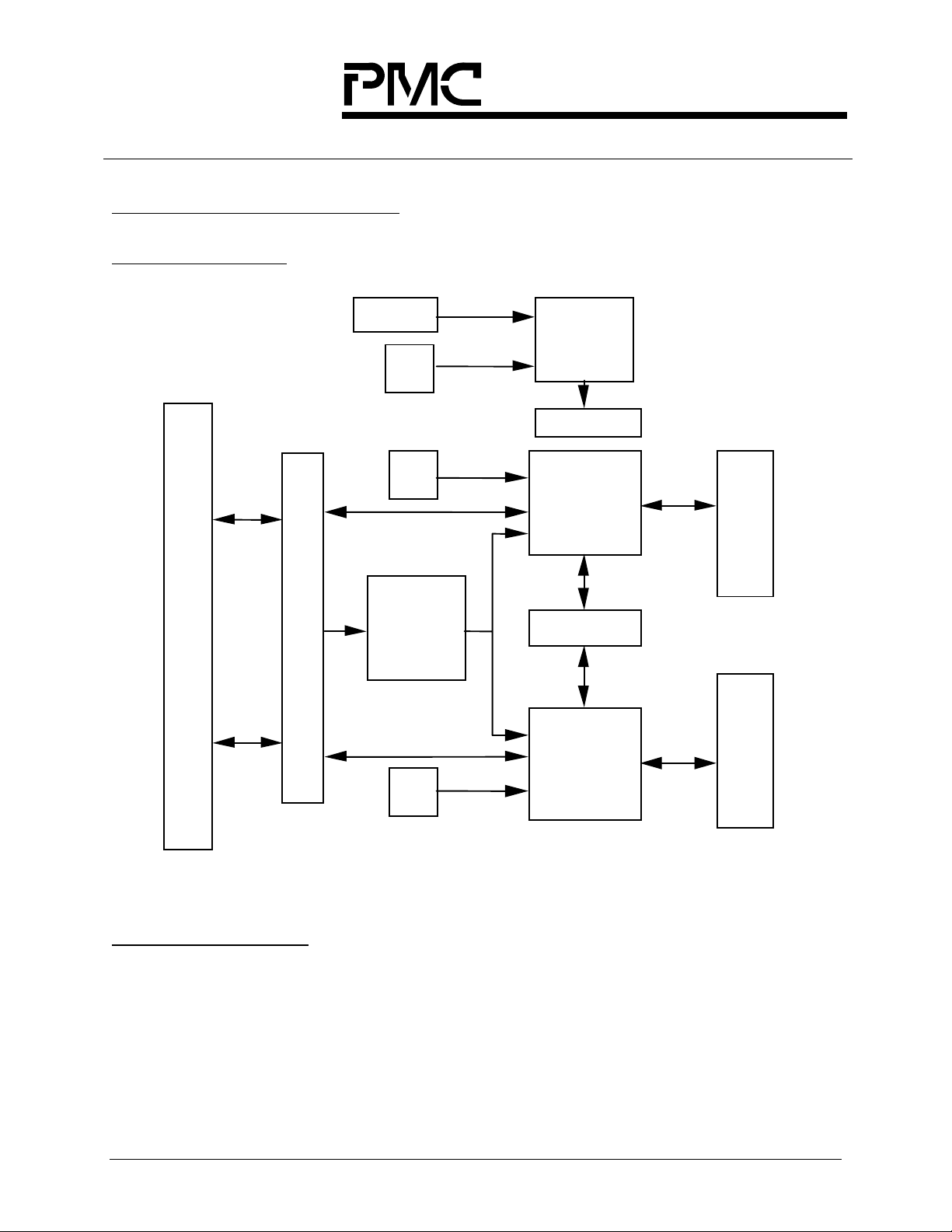
2.1 Block Diagram
DIP Sw.
Clock/PLL
Osc
Clock Hdr
96 Pin Male DIN Connector
Bus Transceivers
Osc
T1XC
Decode
Headers
Logic
T1XC
West
Osc
Figure 1: Block Diagram
East Tx / Rx
Interface
East
West Tx / Rx
Interface
2.2 Bus T ransceivers
Bus transceivers are provided at the connector interface to prevent excessive
loading of the 68HC11 on the EVMB evaluation motherboard. In addition they
provide some measure of isolation for the daughterboard and protection for other
external signals such as the EXTCLK and EXTFP inputs.
2
Page 6

TELECOM STANDARD PRODUCT
PMC-Sierra, Inc.
PMC-920314 ISSUE 2 T1XC EVALUATION DAUGHTERBOARD
PM4541 T1XC-EVBD
2.3 Decode Logic
Decode logic is provided on the daughterboard to give memory mapped access to
all of the registers within both T1XCs. Registers within the "east" T1XC are
accessible starting at address C000H. Registers within the "west" T1XC are
accessible starting at address C100H. Additional chip selects are provided for
addresses C200H-C2FFH and C300H-C3FFH for use on the prototype area.
2.4 DIP Switches
The DIP Switch Block controls the operational modes of the MT8940 DPLL device
that is used to generate the backplane clock. The various modes of the device are
selected by DIP switch settings. Access to the enable inputs for the various clock
outputs is also provided through these switches.
2.5 Clock DPLL
The MT8940 T1/CEPT Digital Trunk DPLL can provide a number of different clocks
with different methods of synchronization, depending upon its mode setting, which
can be used to drive the backplane interface of the T1XCs. The device can output
1.544 MHz, 2.048 MHz, and 4.096 MHz clocks in true or complement format. The
DPLL can be allowed to free-run or it can be synchronized to the receive frame
pulses of either T1XC. PLL control is accomplished with the DIP switches
connected to the inputs.
2.6 Oscillators
Up to four oscillators can be used on the T1XC EVBD daughterboard depending
upon the choice of configuration. The T1XC devices require a 37.056 MHz clock if
all of the device's features are to be utilized. Although two oscillator sockets are
provided, only a single oscillator is necessary if two T1XC devices are used. The
insertion of a jumper (J25) will join the two T1XC XCLK inputs together to allow the
single clock to drive both devices. If an E1XC device is used in place of one of the
T1XC devices then the jumper must be removed to isolate each clock line and a
49.152 MHz oscillator is used to drive the E1XC XCLK input.
The MT8940 DPLL device requires two oscillators to drive internal DPLLs, one at
12.355 MHz, and the other at 16.384 MHz. If the MT8940 is removed from the
daughterboard, then these oscillators can be replaced with ones directly compatible
with the backplane rate. Each oscillator output is directly accessible at header pins,
allowing connections to be made by connecting jumpers to the T1XC devices.
3
Page 7

TELECOM STANDARD PRODUCT
PMC-Sierra, Inc.
PMC-920314 ISSUE 2 T1XC EVALUATION DAUGHTERBOARD
PM4541 T1XC-EVBD
2.7 T1XC Devices
Up to two T1XC devices can be placed on the daughterboard at a time. Each
device runs independent of the other, except when explicit connections are made
through the header strips (i.e. when configured as a jitter attenuating format
converter or "CSU"). All internal registers are individually accessible and each
device has been set up with individual receiver, transmitter and backplane access
through headers and connectors. A full description of the T1XC device is beyond
the scope of this document. For more information, refer to the PM4341 T1XC
datasheet.
2.8 "CSU" Connection Blocks
While the main purpose of the evaluation daughterboard is to provide unrestricted
access to all of the features of the T1XC device, one application is conveniently
provided which allows easy evaluation of most of the features of the device. By
plugging in shorting jumpers into the two 16 pin CSU DIP sockets (U5 and U6) on
the daughterboard, the two T1XCs are connected back to back to implement a jitterattenuating format converter (a function often implemented within a CSU) as
described in the T1XC datasheet. These CSU DIP socket jumpers make almost all
of the necessary connections except for the signals BRCLK, BRFPI, and BTCLK.
Connections for these signals are made through E-W and W-E jumper blocks J19,
J20, J21, J22, J23, and J24. By installing jumper connections between pin 1 and
pin 2 of jumper blocks J19 and J20, between pin 3 and pin 4 of each of jumper
blocks J21, J22, J23, J24, and between pin 2 and 3 of jumper block J30, a "CSU"
like application can be implemented where the 1.544 MHz clock for the backplane
between the two T1XC devices is provided by the MT8940, which in turn is locked to
the recovered clock provided by T1XC #1. Variations of this application can be
explored by using the other options provided on the jumper blocks. With this
application, and with its variations, different backplane rates can be tested.
Connections are provided for 1.544 MHz, 2.048 MHz, and externally supplied
backplane clock rates.
4
Page 8
TELECOM STANDARD PRODUCT
PMC-Sierra, Inc.
PMC-920314 ISSUE 2 T1XC EVALUATION DAUGHTERBOARD
PM4541 T1XC-EVBD
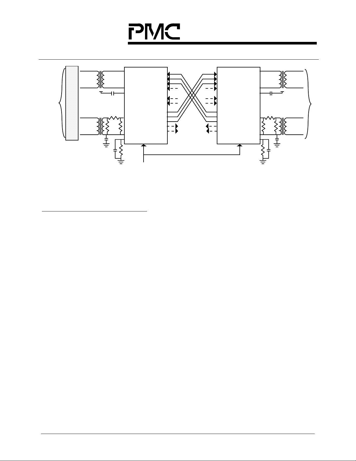
TAP
N
e
t
DSX-1
Transmit
AVD
+
TAN
TC
w
o
r
CSU Analog Interface
k
(not provided on EVBD)
DSX-1
Receive
AVS
RAS
REF
RRC
AVS
BTPCM
BTSIG
BTFP
BTCLK
BRFPI
BRCLK
BRPCM
BRSIG
BRFPO
RCLKO
RFP
PM4341 T1XC
#1
37.056MHz
BTPCM
BTSIG
BTFP
BTCLK
BRFPI
BRCLK
BRPCM
BRSIG
BRFPO
RCLKO
RFP
#2
TAP
TAN
TC
RAS
PM4341 T1XC
REF
RRC
XCLKXCLK
AVS
+
AVD
AVS
Figure 2: Jitter Attenuating "CSU" Application Hookup
2.9 Transmit/Receive Interface
The daughterboard provides three different types of interfaces for the transmit and
receive signals. The two standard analog interfaces provided are a 100 ohm minibantam interface and a 50 ohm BNC interface. The mini-bantams are terminated
with a 100 ohm resistor on the TN/RN pins to prevent an excessive voltage kick
when mini-bantam plugs are inserted or removed. The BNC connector barrel can
optionally be terminated with a resistor to ground, or grounded directly, by stuffing a
resistor or shorting strap in locations R15, R16, R17, and R18. The daughterboard
is shipped with these 4 locations empty, thereby providing a 50Ω BNC interface.
The third interface provided is strictly digital and brings out all of the T1XC's digital
DS-1 signals to header pins for easy test access. When the digital interface is used
each T1XC's analog receiver can be powered down by moving the jumper on
jumper block J31 or J32.
DSX-1
Transmit
DSX-1
Receive
C
u
s
t
o
m
e
r
5
Page 9

TELECOM STANDARD PRODUCT
PMC-Sierra, Inc.
PMC-920314 ISSUE 2 T1XC EVALUATION DAUGHTERBOARD
PM4541 T1XC-EVBD
3 INTERFACE DESCRIPTION
3.1 Edge Connector Interface
The Edge Connector Interface is made up of a male 96 pin DIN of which 64 pins are
actually used. It consists of signals appropriate to read and write to the registers of
the devices on the daughterboard, and it provides the necessary power and ground.
The connections have been specially designed to mate with PMC's PM1501 EVMB
evaluation motherboard. TTL signal levels are used on this interface.
Signal
Name Type
Pin
Function
ALE O C1 Address latch enable. When high, identifies that
address is valid on AD[7:0].
E O C2 Microprocessor Clock
RWB O C3 Active low write, active high read enable
RSTB O C4 Active low H/W reset
A[15] O C5 Address bus bit 15
A[14] O C6 Address bus bit 14
A[13] O C7 Address bus bit 13
A[12] O C8 Address bus bit 12
A[11] O C9 Address bus bit 11
A[10] O C10 Address bus bit 10
A[9] O C11 Address bus bit 9
A[8] O C12 Address bus bit 8
AD[7] I/O C13 Multiplexed address/data bus bit 7
AD[6] I/O C14 Multiplexed address/data bus bit 6
AD[5] I/O C15 Multiplexed address/data bus bit 5
AD[4] I/O C16 Multiplexed address/data bus bit 4
AD[3] I/O C17 Multiplexed address/data bus bit 3
AD[2] I/O C18 Multiplexed address/data bus bit 2
6
Page 10

TELECOM STANDARD PRODUCT
PMC-Sierra, Inc.
PMC-920314 ISSUE 2 T1XC EVALUATION DAUGHTERBOARD
PM4541 T1XC-EVBD
AD[1] I/O C19 Multiplexed address/data bus bit 1
AD[0] I/O C20 Multiplexed address/data bus bit 0
PA3 O C21 68HC11 Processor Port A bit 3
PA4 O C22 68HC11 Processor Port A bit 4
PA5 O C23 68HC11 Processor Port A bit 5
PA6 O C24 68HC11 Processor Port A bit 6
PD2 I C25 MISO. Master In Slave Out of Por t D acting as SPI.
Pulled up on motherboard.
PD3 O C26 MOSI. Master Out Slave In of Port D acting as SPI.
Pulled up on motherboard.
PD4 O C27 SCK. Serial clock of Port D acting as SPI. Pulled up
on motherboard.
PD5 O C28 SS. Slave Select of Po r t D acting as SPI active low.
Pulled up on motherboard.
IRQ I C29 Maskable interrupt
XIRQ I C30 Non Maskable Interrupt
DISB I C31 EVMB memory disable. Pulling this signal low will
disable MPU access to the EVMB's on-board RAM
and EPROM.
SP O C32 SPARE
GND O A1-
Ground
A28
+5V O A29-
+5 Volt s
A32
3.2 Header Connections
All T1XC functional pins are connected to male header strips to provide as much
access as possible. These headers may be used as probe points or as a means to
build sample applications by making appropriate connections between points. Each
T1XC can run in isolation of the other, thus any application, other than the default
sample "CSU", will require header connections to be made.
7
Page 11
TELECOM STANDARD PRODUCT
PMC-Sierra, Inc.
PMC-920314 ISSUE 2 T1XC EVALUATION DAUGHTERBOARD
PM4541 T1XC-EVBD
3.2.1 External Signal Header
This header is provided to accept an exter nal clock and framing pulse source. These
inputs are then buffered for use on the board. External clock sources must be
buffered through this header to avoid possible damage to the T1XCs or DPLL.
Signal Type Ref. Description
EXTFP I J26-2 External Framing Pulse Input
EXTCLK I J26-4 External Clock Input
BEXTFP O J27-1 Buffered External Framing Pulse
BEXTCLK O J27-2 Buffered External Clock
3.2.2 DPLL Header
This header is provided to give access to the clock generating MT8940 DPLL chip
as well as provide direct oscillator access. All of the major DPLL outputs are brought
out to this header even though they may be of limited use with the T1XC (e.g. the
4.096 MHz clock).
Signal Type Ref. Description
FPIN I J29-2 1.544 MHz Framing pulse input to MT8940.
C8KB I/O J29-1 2.048 MHz Framing pulse in/out (mode dependent).
GFP I/O J29-3 8 kHz Framing pulse output from the MT8940. Note
that this active low output signal is derived from the
16.388 MHz clock and has a 244ns pulsewidth. This
frame pulse signal signal should only be routed to
the T1XC when the backplane is configured for
2.048 MHz; this signal is not suitable when the
T1XC backplane is 1.544 MHz.
C1M5 O J29-4 1.544 MHz Output clock from MT8940.
C1M5B O J29-5 Inverted C1M5 clock.
C2M O J29-6 2.048 MHz output clock from MT8940.
C2MB O J29-7 Inverted C2M clock.
C4M O J29-8 4.096 MHz Output clock from MT8940.
8
Page 12
TELECOM STANDARD PRODUCT
PMC-Sierra, Inc.
PMC-920314 ISSUE 2 T1XC EVALUATION DAUGHTERBOARD
PM4541 T1XC-EVBD
C4MB O J29-9 Inverted C4M clock.
C16M O J29-10 Direct access to 16.388 MHz clock driving the
MT8940. This pin is mainly provided for direct
oscillator access. If the MT8940 is not used the
16.388 MHz clock can be replaced by a 2.048 MHz
clock with access to the clock signal provided by
this pin.
C12M O J29-11 Direct access to 12.355 MHz clock driving the
MT8940. This pin is mainly provided for direct
oscillator access. If the MT8940 is not used the
12.355 MHz clock can be replaced by a 1.544 MHz
clock with access to the clock signal provided by
this pin.
GND G J29-12 MT8940 DPLL header ground reference.
3.2.3 T1XC Headers
A number of headers are provided which give direct access to the main functional
pins on the T1XCs. Both devices on the daughterboard have the same pins brought
out to headers and every effort has been made to insure that all headers are
symmetrical with both devices. The T1XCs are uniquely identified by an east/west
designation. The following table gives a brief description of the T1XC signals. For a
more detailed description of the T1XC device, refer to the T1XC datasheet.
Signal Type Ref (E) Ref (W) Description
TAP O J9-1 J10-1 Transmit Analog Positive Pulse
TAN O J9-2 J10-2 Transmit Analog Negative Pulse
RAS I J9-3 J10-3 Receive Analog Signal
REF I/O J9-4 J10-4 Receive Reference
GND G J9-5 J10-5 T1XC Analog Ground Reference
TCLKI I J15-1 J16-1 Transmit Clock Input
TCLKO O J15-2 J16-2 Transmit Clock Output
TDP/TDD O J15-3 J16-3 Transmit Digital Positive Line Pulse/
Transmit Digital DS-1 Signal
TDN/TFLG O J15-4 J16-4 Transmit Digital Negative Line Pulse/
Transmit FIFO Flag
TDLCLK/
TDLUDR
TDLSIG/
TDLINT
O J15-5 J16-5 Transmit Data Link Clock/ Transmit Data
Link Underrun
I/O J15-6 J16-6 Transmit Data Link Signal/ Transmit Data
Link Interrupt
9
Page 13

TELECOM STANDARD PRODUCT
/
PMC-Sierra, Inc.
PMC-920314 ISSUE 2 T1XC EVALUATION DAUGHTERBOARD
PM4541 T1XC-EVBD
GND G J15-7 J16-7 T1XC Digital Transmit Ground Reference
RDLCLK/
RDLEOM
RDLSIG/
RDLINT
O J13-1 J14-1 Receive Data Link Clock/ Receive Data
Link End of Message
O J13-2 J14-2 Receive Data Link Signal/ Receive Data
Link Interrupt
RCLKI I J13-3 J14-3 Receive Line Clock Input
RDP/ RDD/
SDP
I/O J13-4 J14-4 Receive Digital Positive Line Pulse/
Receive Digital DS-1 Signal/ Sliced
Positive Line Pulse
RDN/ RLCV
SDN
I/O J13-5 J14-5 Receive Digital Negative Line Pulse/
Receive Line Code Violation Indication/
Sliced Negative Line Pulse
GND G J13-6 J14-6
BTPCM/
BTDP
BTSIG/
BTDN
I J11-4 J12-4 Backplane Transmit PCM/ Backplane
Transmit Positive Line Pulse
I J11-3 J12-3 Backplane Transmit Signaling/ Backplane
Transmit Negative Line Pulse
BTFP I J11-2 J12-2 Backplane Transmit Frame Pulse
BTCLK I J11- 1 J12-1 Backplane Transmit Clock
GND G J11-5 J12-5 Backplane Transmit Header Ground
Reference
BRCLK I J17-1 J18-1 Backplane Receive Clock
BRFPI I J17-2 J18-2 Backplane Frame Pulse Input
BRPCM/
BRDP
BRSIG/
BRDN
O J17-3 J18-3 Backplane Receive PCM/ Backplane
Receive Positive Line Pulse
O J17-4 J18-4 Backplane Receive Signaling/ Backplane
Receive Negative Line Pulse
BRFPO O J17-5 J18-5 Backplane Frame Pulse Output
RDPCM/
RPCM
O J17-6 J18-6 Recovered Decoded PCM/ Recovered
PCM
RCLKO O J17-7 J18-7 Recovered PCM Clock Output
RFP O J17-8 J18-8 Receive Frame Pulse
GND G J17-9 J18-9 Backplane Receive Ground Reference
3.2.4 Prototype Chip Select Header
Two unused chip selects from the decoding logic are provided on a header near the
prototype area.
10
Page 14
TELECOM STANDARD PRODUCT
PMC-Sierra, Inc.
PMC-920314 ISSUE 2 T1XC EVALUATION DAUGHTERBOARD
PM4541 T1XC-EVBD
Signal Type Ref. Description
Spare1_CSB O J28-1 Spare CSB pin address (C2XX)
Spare2_CSB O J28-2 Spare CSB pin address (C3XX)
3.3 DIP Switches
One 8 bit dip switch is provided on the daughterboard. This switch controls the
operating modes of MT8940 PLL chip and the output enables for the various clock
outputs. When open, each bit line is pulled high. When closed, the bit lines are
individually pulled to ground. For a brief description of the MT8940 operating
modes, consult the tables in the Clock PLL implementation description section.
Switch ID Mapping
Clock 1 MS0
Clock 2 MS1
Clock 3 MS2
Clock 4 MS3
Clock 5 ENC2O
Clock 6 ENCV
Clock 7 ENC4O
Clock 8 Unused
11
Page 15

TELECOM STANDARD PRODUCT
PMC-Sierra, Inc.
PMC-920314 ISSUE 2 T1XC EVALUATION DAUGHTERBOARD
PM4541 T1XC-EVBD
4 PHYSICAL DESCRIPTION
4.1 Characteristics
The T1XC EVBD is an evaluation board that allows the T1XC device to be feature
tested and evaluated for various applications. Special consideration has been made
in its design to allow testing of the E1XC when it is available. While the daughterboard can be used standalone with a limited feature set, it has been especially
designed to link with PMC's EVMB (Evaluation Motherboard). The EVMB controller
board provides a microprocessor to read and write to all of the T1XC's internal
registers allowing configuration, control and set-up of the various modes of T1XC
operation.
The T1XC EVBD is laid out for convenient bench top use for test or demonstration
purposes. It is provided with rubber feet that are placed to avoid PCB flexing. Pin
headers provide easy access to all signals necessary during device testing. A
T1/CEPT Digital PLL is installed to provide the necessary 1.544 MHz or 2.048 MHz
backplane rates. External pins allow access when using an externally generated
backplane clock. Ground pins for scope probes are conveniently provided and
distributed. Simple configuration into the example CSU application is provided. The
DIP switches, pin headers, and interface connections are labeled on the silkscreen
for easy identification and ample prototype area is provided. The size of the T1XC
EVBD is constrained to 8.5 x 6.5 inches and, when mated with the EVMB card, will
fit in a standard three ring binder.
12
Page 16

TELECOM STANDARD PRODUCT
PMC-Sierra, Inc.
PMC-920314 ISSUE 2 T1XC EVALUATION DAUGHTERBOARD
PM4541 T1XC-EVBD
4.2 Layout
8940
DIP SW
External
CLK/FP
BUS TRANSCEIVERS
96 Pin Male DIN
Oscillators
T1XC #1
Osc
Glue Logic
E-W
Jumpers
CLK
MT8940
8940
HDR
T1XC #1
(EAST)
Backplane Headers
CSU Config DIPS
Backplane Headers
T1XC #2
(WEST)
Transformer
RXAnalog
TX/RX Header
W-E
Jumpers
RXAnalog
Power
TX/RX Header
Bantam R/C
BNC
Mini-Bantam
Power
BNC
Mini-Bantam
Bantam R/C
BNC
Mini-Bantam
Transformer
BNC
T1XC #2
Osc
Mini-Bantam
PROTOTYPE AREA
Figure 3: Board Layout
13
Page 17

TELECOM STANDARD PRODUCT
PMC-Sierra, Inc.
PMC-920314 ISSUE 2 T1XC EVALUATION DAUGHTERBOARD
PM4541 T1XC-EVBD
5 D.C. CHARACTERISTICS
Symbol Parameter Min Max Units Test Conditions
V
I
5DC
T
5DC
A
+5V DC Power
Supply Voltage
+5V DC Power
Supply Current
Ambient
Temperature
4.5 5 .5 V
3A V
050°CV
= 5.0 V + 10%
5DC
= 5.0 V + 10%
DC
14
Page 18

TELECOM STANDARD PRODUCT
PMC-Sierra, Inc.
PMC-920314 ISSUE 2 T1XC EVALUATION DAUGHTERBOARD
PM4541 T1XC-EVBD
6 IMPLEMENTATION DESCRIPTION
6.1 Bus T ransceivers
Bus Transceivers have been used on the daughterboard to minimize the loading
presented to the motherboard microprocessor. Two 74HCT244's buffer all eight
upper address bits, the microprocessor control signals, and the external clock and
framing pulse inputs. A single 74HCT245 provides the bi-directional buffering of the
multiplexed address/data bus. All motherboard signals from the 96-pin DIN
connector have been tied through SIPs to insure proper standalone operation. The
standard techniques outlined in the EVMB datasheet for implementing the decoding
and buffering has been followed.
6.2 Decode Logic
The decode logic provides the address mapping of all internal registers of both
T1XC's as well as providing generation of the required RDB and WRB signals.
Again the implementation of the decode logic has followed the techniques outlined
in the EVMB datasheet. T1XC #1 (EAST) is mapped starting at address C000H and
T1XC #2 (WEST) is mapped starting at address C100H. Two unused chip selects,
active for address ranges C200-C2FFH and C300-C3FFH, are available for use on
the prototype section. The full register map is given below:
East T1XC West T1XC Description
C000H C100H T1XC Receive Options
C001H C101H T1XC Receive Backplane Options
C002H C102H T1XC Datalink Options
C003H C103H T1XC Receive DS1 Interface Configuration
C004H C104H T1XC Transmit DS1 Interface Configuration
C005H C105H T1XC Transmit Backplane Options
C006H C106H T1XC Transmit Framing and Bypass Options
C007H C107H T1XC Transmit Timing Options
C008H C108H T1XC Master Interrupt Source #1
C009H C109H T1XC Master Interrupt Source #2
C00AH C10AH T1XC Master Diagnostics
C00BH C10BH T1XC Master Test
C00CH C10CH T1XC Revision/Chip ID
C00DH C10DH T1XC Master Reset
C00EH C10EH T1XC Phase Status Word (LSB)
C00FH C10FH T1XC Phase Status Word (MSB)
15
Page 19

TELECOM STANDARD PRODUCT
PMC-Sierra, Inc.
PMC-920314 ISSUE 2 T1XC EVALUATION DAUGHTERBOARD
PM4541 T1XC-EVBD
C010H C110H CDRC TSB Configuration
C011H C111H CDRC TSB Interrupt Enable
C012H C112H CDRC TSB Interrupt Status
C014H C114H XPLS TSB Line Length Configuration
C015H C115H XPLS TSB Control/Status
C016H C116H XPLS TSB CODE Indirect Address
C017H C117H XPLS TSB CODE Indirect Data
C018H C118H DJAT TSB Interrupt Status
C019H C119H DJAT TSB Reference Clock Divisor (N1) Control
C01AH C11AH DJAT TSB Output Clock Divisor (N2) Control
C01BH C11BH DJAT TSB Configuration
C01CH C11CH ELST TSB Configuration
C01DH C11DH ELST TSB Interrupt Enable/Status
C01EH C11EH ELST TSB Trouble Code
C020H C120H FRMR TSB Configuration
C021H C121H FRMR TSB Interrupt Enable
C022H C122H FRMR TSB Interrupt Status
C02AH C12AH RBOC TSB Enable
C02BH C12BH RBOC TSB Code Status
C02CH C12CH ALMI TSB Configuration
C02DH C12DH ALMI TSB Interrupt Enable
C02EH C12EH ALMI TSB Interrupt Status
C02FH C12FH ALMI TSB Alarm Detection Status
C030H C130H TPSC TSB Configuration
C031H C131H TPSC TSB µP Access Status
C032H C132H TPSC TSB Channel Indirect Address/Control
C033H C133H TPSC TSB Channel Indirect Data Buffer
C034H C134H XFDL TSB Configuration
C035H C135H XFDL TSB Interrupt Status
C036H C136H XFDL TSB Transmit Data
C038H C138H RFDL TSB Configuration
C039H C139H RFDL TSB Interrupt Status/Control
C03AH C13AH RFDL TSB Status
C03BH C13BH RFDL TSB Receive Data
C03CH C13CH IBCD TSB Configuration
C03DH C13DH IBCD TSB Interrupt Enable/Status
C03EH C13EH IBCD TSB Activate Code
C03FH C13FH IBCD TSB Deactivate Code
C040H C140H SIGX TSB Configuration
C041H C141H SIGX TSB µP Access Status
C042H C142H SIGX TSB Channel Indirect Address/Control
16
Page 20

TELECOM STANDARD PRODUCT
PMC-Sierra, Inc.
PMC-920314 ISSUE 2 T1XC EVALUATION DAUGHTERBOARD
PM4541 T1XC-EVBD
C043H C143H SIGX TSB Channel Indirect Data Buffer
C044H C144H XBAS TSB Configuration
C045H C145H XBAS TSB Alarm Transmit
C046H C146H XBAS TSB Control
C047H C147H XIBC TSB Loopback Code
C049H C149H PMON TSB Interrupt Enable/Status
C04AH C14AH PMON TSB LCV Count (LSB)
C04BH C14BH PMON TSB LCV Count (MSB)
C04CH C14CH PMON TSB BEE Count (LSB)
C04DH C14DH PMON TSB BEE Count (MSB)
C04EH C14EH PMON TSB FER Count
C04FH C14FH PMON TSB OOF/COFA Count
C050H C150H RPSC TSB Configuration
C051H C151H RPSC TSB µP Access Status
C052H C152H RPSC TSB Channel Indirect Address/Control
C053H C153H RPSC TSB Channel Indirect Data Buffer
C055H C155H PDVD TSB Interrupt Enable/Status
C057H C157H XBOC TSB Code
C059H C159H XPDE TSB Interrupt Enable/Status
C05DH C15DH RSLC TSB Interrupt Enable/Status
17
Page 21

TELECOM STANDARD PRODUCT
PMC-Sierra, Inc.
PMC-920314 ISSUE 2 T1XC EVALUATION DAUGHTERBOARD
PM4541 T1XC-EVBD
BALE
BE_CLOCK
BRWB
BA[15:8]
BAD[7:0]
T1XC_RDB
HCT245 DIR
T1XC_WRB
T1XC_CSB
BA="C0";
BRWB=1
A[7:0]
READ CYCLE
BA °"C0";
BRWB=1
DOUT
DOUTA[7:0] DINA[7:0] DINA[7:0]
Figure 4: Decode Logic Waveforms
BA="C0";
BRWB=0
WRITE CY CLE
BA °"C0";
BRWB=0
6.3 Clock PLL and DIP Switches
One Mitel MT8940 provides all clocks necessary to drive the various backplane
rates supported by the T1XC. The MT8940 is a dual digital PLL which can provide
timing and synchronization signals for T1 or CEPT transmission links and the STBUS . The first PLL provides the T1 clock (1.544 MHz) synchronized to an input
framing pulse. The second PLL provides CEPT or ST-BUS timing signals
synchronized to an internal or external framing pulse signal. For a more detailed
description of the device, refer to the datasheet on the MT8940 in the Mitel
Semiconductor Databook.
All outputs of the MT8940 are either brought out to header blocks or routed to the
CSU connector DIP sockets. A single 8-position DIP switch provides control over the
mode of the MT8940 device as well as control over the output clock enables. If the
MT8940 is not used, it can be removed from the daughterboard and its oscillators
can be replaced with 1.544 MHz and 2.048 MHz devices. The PLL oscillator clock
outputs are conveniently brought out to the header strip for use on the
daughterboard.
The mapping of the DIP switches to the MT8940 ports is as follows:
18
Page 22

TELECOM STANDARD PRODUCT
PMC-Sierra, Inc.
PMC-920314 ISSUE 2 T1XC EVALUATION DAUGHTERBOARD
PM4541 T1XC-EVBD
Switch ID Label Mapping
SW1-1 MS0 MS0 (Mode Select '0')
SW1-2 MS1 MS1 (Mode Select '1')
SW1-3 MS2 MS2 (Mode Select '2')
SW1-4 MS3 MS3 (Mode Select '3')
SW1-5 ENC2 ENC20 (Active high enable control for pins
C2O and C2OB )
SW1-6 ENCV ENCV (Active high enable control for pins
CV and CVB )
SW1-7 ENC4 ENC40 (Active high enable control for pins
C4O and C4OB )
SW1-8 Unused
Setting these switches selects the operating mode for the MT8940, as described below:
Mode # MS[0:3] DPLL #1 Operating Mode DPLL #2 Operating Mode
0 0000 Normal Mode:
Externally applied 4.096
MHz. clock and 8 kHz.
Generates the 1.544 MHz
T1 clock synchronized to
the falling edge of the input
framing pulse.
1 0001 Normal Mode
Operates as above.
frame pulse, properly phase
related, are used to
generate the 2.048 MHz
output clock.
Normal Mode:
Generates the CEPT (STBUS) timing signals locked
to the 8 kHz input signal
(C8KB)
2 0010 Normal Mode
Externally applied 4.096
MHz. clock is used to
Operates as above.
generate the 2.048 MHz
output clock and 8 kHz
frame pulse.
3 0011
DEFAULT
CONFIG
Normal Mode
Operates as above.
Normal Mode
Generates the CEPT (ST-
BUS) timing signals locked
to the 8 kHz input signal
(C8KB)
19
Page 23

TELECOM STANDARD PRODUCT
PMC-Sierra, Inc.
PMC-920314 ISSUE 2 T1XC EVALUATION DAUGHTERBOARD
PM4541 T1XC-EVBD
4 0100 Divide-1 Mode:
Externally applied 4.096
MHz. clock and 8 kHz.
Divides the CVB input
signal by 193. The divided
output is connected to
DPLL #2
5 0101 Divide-1 Mode
Operates as above
frame pulse, properly phase
related, are used to
generate the 2.048 MHz
output clock.
Single Clock-1 Mode:
Provides the CEPT/ST-BUS
compatible timing signals
locked to an 8 kHz. internal
signal provided by DPLL
#1.
6 0110 Divide-1 Mode Same as 'mode 2'
7 0111 Divide-1 Mode Single Clock-1 Mode
8 1000 Normal Mode Same as 'mode 0'
9 1001 Normal Mode F0B becomes an input.
DPLL #2 provides the ST-
BUS signals locked onto
F0B input only if it is 16
kHz.
10 1010 Normal Mode Same as 'mode 2'
11 1011 Normal Mode Free Run Mode
Provides the CEPT/ST-BUS
compatible timing and
framing signals with no
external inputs other than
the master clock.
12 1100 Divide-2 Mode:
Same as 'mode 0'
Divides the CVB input by
256. The divided output is
connected to DPLL #2
13 1101 Divide-2 Mode Single Clock-2 Mode:
Provides the CEPT/ST-BUS
signals locked to the 8 kHz.
internal signal provided by
DPLL #1
14 1110 Divide-2 Mode Same as 'mode 2'
15 1111 Divide-2 Mode Single Clock-2 Mode
20
Page 24

TELECOM STANDARD PRODUCT
PMC-Sierra, Inc.
PMC-920314 ISSUE 2 T1XC EVALUATION DAUGHTERBOARD
PM4541 T1XC-EVBD
6.4 T1XC
Two T1XCs can be socketed into the daughterboard. Each is individually accessible
and can run independently of the other. All pins except for the microprocessor
interface and power pins are connected to header strips for easy test equipment
access. Analog receive power pin RAVD is connected to a jumper to enable tying to
either ground or power. Tying this pin to ground will disable the internal RSLC TSB,
reducing the power consumed. Tying the RAVD pin to VCC enables the normal
operating mode. All other power pins are appropriately decoupled and all inputs are
tied high through 10 kΩ resistors SIPs.
For a more detailed description of the T1XC and its features, refer to the T1XC
Standard Product datasheet.
6.5 "CSU" DIPs and Jumpers
Normally, the two T1XCs run independently of each other except when explicit
connections are made between the two devices. To facilitate testing of a simple
application involving two devices appropriate control signals have been wired to two
16 pin DIP sockets and six jumpers to enable hooking up the T1XCs in a "CSU"-like
application.
Both T1XCs are connected in a symmetrical fashion and most connections are
completed by installing shorting bar jumpers into the two 16 pin DIP sockets labeled
for the CSU set-up. The remaining unconnected signals are BRCLK, BRFPI, and
BTCLK. By installing jumpers across pins 1 and 2 of each of jumper blocks J19 and
J20, between pins 3 and 4 of each of the jumper blocks J21, J22, J23, J24, and
between pin 2 and 3 of jumper block J30, a "CSU" like application can be
implemented where the 1.544 MHz clock for the backplane between the two T1XC
devices is provided by the MT8940, which in turn is locked to the recovered clock
provided by T1XC #1. Bits 1 and 2 of SW1 must be closed; the remaining bits open.
By appropriately making jumper connections to the other available clock options, the
backplane can be run at different rates, such as 1.544 MHz, 2.048 MHz, or at an
externally supplied clock rate.
21
Page 25

TELECOM STANDARD PRODUCT
PMC-Sierra, Inc.
PMC-920314 ISSUE 2 T1XC EVALUATION DAUGHTERBOARD
J21
PM4541 T1XC-EVBD
"N
E
T
W
O
R
K"
DSX-1
Transmit
Interface
DSX-1
Receive
Interface
TAP
TAN
RAS
REF
BEXTCLK
C2M
C1M5
BEXTFP
GFP
BTPCM
BTSIG
BTFP
BTCLK
BRFPI
BRCLK
BRPCM
BRSIG
T1XC #1 (East)
BRFPO
RCLKO
RFP
RFP
J30
J24
J20
EW CSU JUMPER
J19
J22
BTPCM
BTSIG
BTFP
BTCLK
BRFPI
BRCLK
BRPCM
BRSIG
BRFPO
RCLKO
WE CSU JUMPER
RFP
T1XC #2 (West)
GFP
BEXTFP
C1M5
C2M
BEXTCLK
TAP
TAN
RAS
REF
DSX-1
Transmit
Interface
DSX-1
Receive
Interface
C
U
S
T
O
M
E
R
J23
Figure 5: "CSU" Circuit Overview
6.6 Transmit/Receive Interfaces
Three different transmit and receive interfaces are provided on the daughterboard.
The digital interface can be used by connecting to the two header blocks
immediately adjacent to each T1XC. Header blocks J13 and J15 provide the digital
interface for the east T1XC while headers J14 and J16 provide the interface for the
west T1XC. Before making use of these pins, the analog receiver of each T1XC
22
Page 26

TELECOM STANDARD PRODUCT
PMC-Sierra, Inc.
PMC-920314 ISSUE 2 T1XC EVALUATION DAUGHTERBOARD
PM4541 T1XC-EVBD
should be disabled. This is done by moving the jumpers on J31 and J3, which
provide power to RAVD, to the grounding position.
Two DSX-1 analog interfaces are also provided. Both the transmit and receive DSX1 interfaces on each T1XC can be connected to either a mini-bantam or BNC
connector. The analog transmit and receive interface are passed through a 1:1.36
and 2:1 transformer, respectively, and then connected to either Bantam or BNC
connectors. The mini-bantam is terminated with a 100 ohm resistor to prevent
"kick-back" when a plug is inserted or removed from the jack. The BNC interface is
a standard 50 ohm coax with stuffing options for ground or resistor connections
across the shield (or barrel). While some test equipment may require a 75 ohm
interface, a 50 ohm connection should not cause any appreciable mismatch for test
frequencies used by the T1XC or E1XC devices.
23
Page 27

TELECOM STANDARD PRODUCT
PMC-Sierra, Inc.
PMC-920314 ISSUE 2 T1XC EVALUATION DAUGHTERBOARD
PM4541 T1XC-EVBD
7 T1XC DAUGHTERBOARD FIRMWARE DESCRIPTION
The EVMB evaluation board provides a serial interface for hooking up a standard
"VT100" type terminal. The RF2 SERIAL 25-pin D-type connector on the EVMB is
configured as a DCE, 9600 BAUD, 8 bit, NO PARITY, one STOP bit. Connecting a
terminal to this port, setting switch 2 on the MODE switch bank to CLOSED and
pressing the RESET switch on the EVMB will enable console control.
When the system is started cold or after a hardware reset, the first output to the
console will be the Forth kernel identification followed by a prompt:
Max-FORTH vX.X
>
The first commands that should be downloaded into the system after a cold boot
should be (note: each line must be terminated with a "carriage return"; the text within
parenthesis are comments and do not have to be typed in):
HEX ( Set up Hex number base )
100 TIB ! ( Relocate text input buffer to eRAM address
100H )
50 TIB 2+ ! ( Define 80 character text input buffer length )
200 DP ! ( Set up Dictionary Pointer )
After inputting each of these commands followed by a carriage return, the FORTH
interpreter should respond with an "OK" signifying it has accepted it. Any failure to
properly input these set-up statements will be characterized by a "?" response from
the interpreter and/or by errors when inputting any subsequent data. Further, if an
error occurred while entering the commands to relocate the text input buffer or
redefine its length, the text buffer will be unable to accept more than the default 16
characters per line input.
The following Forth code was developed for the T1XC daughterboard and presented
here as an example. To set-up the T1XC, all that is minimally required is the above
EVMB initialization words, the register address CONSTANT definitions, and the RD
and WR routines. The remaining words are useful for exercising the more advanced
features of the T1XC.
( Define addresses of TSBs for T1XC #1: EAST )
C000 CONSTANT RXOPT
C001 CONSTANT RXBPOPT
C002 CONSTANT DLOPT
C003 CONSTANT RXDS1
24
Page 28

TELECOM STANDARD PRODUCT
PMC-Sierra, Inc.
PMC-920314 ISSUE 2 T1XC EVALUATION DAUGHTERBOARD
PM4541 T1XC-EVBD
C004 CONSTANT TXDS1
C005 CONSTANT TXBPOPT
C006 CONSTANT TXBYP
C007 CONSTANT TIMOPT
C008 CONSTANT INT1SRC
C009 CONSTANT INT2SRC
C00A CONSTANT DIAG
C00B CONSTANT MTEST
C00C CONSTANT REVID
C00D CONSTANT MRST
C00E CONSTANT PSWL
C00F CONSTANT PSWH
C010 CONSTANT CDRC
C014 CONSTANT XPLS
C018 CONSTANT DJAT
C01C CONSTANT ELST
C020 CONSTANT FRMR
C02A CONSTANT RBOC
C02C CONSTANT ALMI
C030 CONSTANT TPSC
C034 CONSTANT XFDL
C038 CONSTANT RFDL
C03C CONSTANT IBCD
C040 CONSTANT SIGX
C044 CONSTANT XBAS
C046 CONSTANT XIBC
C048 CONSTANT PMON
C050 CONSTANT RPSC
C054 CONSTANT PDVD
C056 CONSTANT XBOC
C058 CONSTANT XPDE
C05C CONSTANT RSLC
C04A CONSTANT LCLK
B02F CONSTANT SCDR
( Addresses for T1XC #2: WEST )
( uncomment if used )
( C100 CONSTANT RXOPT2 )
( C101 CONSTANT RXBPOPT2 )
( C102 CONSTANT DLOPT2 )
( C103 CONSTANT RXDS12 )
( C104 CONSTANT TXDS12 )
( C105 CONSTANT TXBPOPT2 )
( C106 CONSTANT TXBYP2 )
( C107 CONSTANT TIMOPT2 )
( C108 CONSTANT INT1SRC2 )
( C109 CONSTANT INT2SRC2 )
( C10A CONSTANT DIAG2 )
( C10B CONSTANT MTEST2 )
25
Page 29

TELECOM STANDARD PRODUCT
PMC-Sierra, Inc.
PMC-920314 ISSUE 2 T1XC EVALUATION DAUGHTERBOARD
PM4541 T1XC-EVBD
( C10C CONSTANT REVID2 )
( C10D CONSTANT MRST2 )
( C10E CONSTANT PSWL2 )
( C10F CONSTANT PSWH2 )
( C110 CONSTANT CDRC2 )
( C114 CONSTANT XPLS2 )
( C118 CONSTANT DJAT2 )
( C11C CONSTANT ELST2 )
( C120 CONSTANT FRMR2 )
( C12A CONSTANT RBOC2 )
( C12C CONSTANT ALMI2 )
( C130 CONSTANT TPSC2 )
( C134 CONSTANT XFDL2 )
( C138 CONSTANT RFDL2 )
( C13C CONSTANT IBCD2 )
( C140 CONSTANT SIGX2 )
( C144 CONSTANT XBAS2 )
( C146 CONSTANT XIBC2 )
( C148 CONSTANT PMON2 )
( C150 CONSTANT RPSC2 )
( C154 CONSTANT PDVD2 )
( C156 CONSTANT XBOC2 )
( C158 CONSTANT XPDE2 )
( C15C CONSTANT RSLC2 )
( C14A CONSTANT LCLK2 )
( Define Register Offset words )
( Most TSBS follow this standard )
: CONFIG ; ( --- )
: ENABLE 1+ ; ( addr --- addr+1 )
: STATUS 2+ ; ( addr --- addr+2 )
: DATA 3 + ; ( addr --- addr+3 )
( Read memory address, or register, contents )
( Usage: ADDRESS RD <return> )
: RD ( addr --- )
C@ ." =" U.
." HEX" CR ;
( Write memory address, or register, contents )
( Usage: ADDRESS DATA WR <return> )
: WR ( addr data --- )
SWAP C! ;
( Print 1 or 0 to screen, depending on stack value )
26
Page 30

TELECOM STANDARD PRODUCT
PMC-Sierra, Inc.
PMC-920314 ISSUE 2 T1XC EVALUATION DAUGHTERBOARD
PM4541 T1XC-EVBD
: DBIT ( bitfld --- )
0> IF 1
ELSE 0 THEN . ;
: .CR . CR ;
( Print in Right Justified format using 5 character wide field
)
: .RCR 5 .R CR ;
( VT100 clear screen by sending )
( ESC[H and ESC[J )
: CLS ( --- )
1B EMIT 5B EMIT 48 EMIT
1B EMIT 5B EMIT 4A EMIT ;
: HDLC ( --- )
( Read RFDL status and data regs )
( waiting for interrupt. When INT)
( recv'd, echo data to screen and)
( display status bits. Continues )
( in a loop until any key on the )
( keyboard is pressed. )
CR
02 RFDL ENABLE C! ( enable RFDL )
01 RFDL C!
BEGIN
RFDL ENABLE C@ 01 AND 0> IF
RFDL DATA C@ DUP ." DATA=" U.
." (" EMIT ." ) "
RFDL STATUS C@ DUP
." OVR=" 40 AND DBIT DUP
." FLG=" 20 AND DBIT DUP
." EOM=" 10 AND DBIT DUP
." CRC=" 08 AND DBIT
." NVB=" 07 AND DECIMAL .CR
HEX
THEN
?TERMINAL
UNTIL
SCDR C@ DROP ( remove key pressed )
( from uP input reg )
00 RFDL C! ; ( disable RFDL )
: RDPERF ( --- )
( Generates a LCLK strobe to PMON )
27
Page 31

TELECOM STANDARD PRODUCT
PMC-Sierra, Inc.
PMC-920314 ISSUE 2 T1XC EVALUATION DAUGHTERBOARD
PM4541 T1XC-EVBD
( to latch and transfer counter )
( values. Counts are displayed in )
( decimal. )
LCLK 0 WR ( strobe LCLK )
PMON 2+ DUP @ >< 0FFF AND SWAP
2+ DUP @ >< 01FF AND SWAP
2+ DUP C@ 1F AND SWAP
1+ C@ 07 AND DECIMAL CR
." OOF=" .RCR
." FER=" .RCR
." BEE=" .RCR
." LCV=" .RCR HEX ;
( Define word to check TPSC BUSY )
: TBUSY? ( --- FLAG )
TPSC 1+ C@ 80 AND 0> ;
( Define word to check RPSC BUSY )
: RBUSY? ( --- FLAG )
RPSC 1+ C@ 80 AND 0> ;
: IDL
FFF 0 DO LOOP ;
( Define word to indirectly write TPSC )
: TWIND ( ADDR DATA --- )
TPSC 3 + C! ( PUT DATA IN IND DATA REG )
7F AND ( SET R/WB BIT LOW )
TPSC 2+ C! ( PUT ADDR IN IND ADDR REG )
IDL
BEGIN TBUSY? WHILE REPEAT ;
( Define word to indirectly READ TPSC )
: TRIND ( ADDR --- DATA )
80 OR ( SET R/WB BIT HIGH )
TPSC 2+ C! ( PUT ADDR IN IND ADDR REG )
IDL
BEGIN TBUSY? WHILE REPEAT
TPSC 3 + C@ ;
( Define word to initialize TPSC to all zeros )
: TINIT
49 1 DO I 0 TWIND LOOP ;
28
Page 32

TELECOM STANDARD PRODUCT
PMC-Sierra, Inc.
PMC-920314 ISSUE 2 T1XC EVALUATION DAUGHTERBOARD
PM4541 T1XC-EVBD
( Define XMIT DMW on given channel )
: TDMW ( CHAN --- )
20 TWIND ;
( Define word to indirectly write RPSC )
: RWIND ( ADDR DATA --- )
RPSC 3 + C! ( PUT DATA IN IND DATA REG )
7F AND ( SET R/WB BIT LOW )
RPSC 2+ C! ( PUT ADDR IN IND ADDR REG )
IDL
BEGIN RBUSY? WHILE REPEAT ;
( Define word to indirectly READ RPSC )
: RRIND ( ADDR --- DATA )
80 OR ( SET R/WB BIT HIGH )
RPSC 2+ C! ( PUT ADDR IN IND ADDR REG )
IDL
BEGIN RBUSY? WHILE REPEAT
RPSC 3 + C@ ;
( Define word to initialize RPSC to all zeros )
: RINIT
49 1 DO I 0 RWIND LOOP ;
( Define XMIT DMW on given channel )
: RDMW ( CHAN --- )
20 RWIND ;
( Define programmable idle loop )
: PIDL ( DELAY --- )
0 DO LOOP ;
: POLL ( --- )
( Read PMON data regs. Continues in a loop )
( until any key on the keyboard is pressed. )
( Data is displayed on screen in tabular form )
( and is updated approx every second. )
( Data changes dynamically. )
CLS
0
BEGIN
1B EMIT 5B EMIT 48 EMIT
DUP ." TIME=" DECIMAL . HEX
1+
RDPERF
IDL IDL IDL IDL F7F PIDL
?TERMINAL
29
Page 33

TELECOM STANDARD PRODUCT
PMC-Sierra, Inc.
PMC-920314 ISSUE 2 T1XC EVALUATION DAUGHTERBOARD
PM4541 T1XC-EVBD
UNTIL
SCDR C@ DROP ; ( remove key pressed )
( from uP input reg )
( Define word to write XPLS D/A code value )
: XWR ( DATA ADDR --- )
XPLS 2+ C! ( SELECT CODE REG )
XPLS 3 + C! ; ( WRITE CODE VALUE)
( Define word to READ XPLS D/A code value )
: XRD ( ADDR --- )
XPLS 2+ C! ( SELECT CODE REG )
XPLS 3 + C@ ( READ CODE VALUE)
U. ." " ;
( Write complete template values to XPLS )
( Usage: Value1 Value2 ... Value8 WRTEMPL )
: WRTEMPL ( C1 C2 C3 C4 C5 C6 C7 C8 --- )
8 0 DO 7 I - XWR LOOP ;
( Read all template values from XPLS )
( Usage: RDTEMPL )
( uP response: Value1 Value2 ... Value8 )
( [in HEX] )
: RDTEMPL ( --- )
8 0 DO I XRD LOOP ;
To use these functions, use the following syntax (the interpreter response is shown
in italics):
FRMR STATUS RD
= FF HEX
( Read T1XC #1 FRMR reg #2 contents
)
OK
XBAS 10 WR OK ( Write 10 hex to T1XC #1 XBAS reg
0 )
This document is not intended to give a full tutorial in FORTH, which is better
covered in the many FORTH books available. The FORTH kernel on the 68HC11
on the EVMB is based upon the FORTH-83 standard and should be upward
compatible from FORTH-79. For a complete, detailed FORTH tutorial, refer to the
manuals listed in the references.
30
Page 34

TELECOM STANDARD PRODUCT
PMC-Sierra, Inc.
PMC-920314 ISSUE 2 T1XC EVALUATION DAUGHTERBOARD
PM4541 T1XC-EVBD
8 STOCK LIST
Item Qty Reference Description
1
C1,
Not Installed
C4
2
2C2,
0.68 µF ceramic capacitor, 0.3" spacing, 100VDC
C5
3
2C3,
0.1 µF ceramic capacitor, 0.3" spacing, 100VDC
C6
4
2C7,
47 nF ceramic capacitor, 0.2" spacing, 100VDC
C8
5
2C9,
470 nF ceramic capacitor, 0.2" spacing, 100VDC
C10
6
25 C11,
0.01 µF ceramic Capacitor, 0.2" spacing, 100VDC
C12,
C13,
C14,
C15,
C16,
C17,
C18,
C19,
C20,
C21,
C22,
C23,
C24,
C25,
C26,
C27,
C28,
C29,
C30,
C31,
C32,
C33,
C34,
C35
31
Page 35

TELECOM STANDARD PRODUCT
PMC-Sierra, Inc.
PMC-920314 ISSUE 2 T1XC EVALUATION DAUGHTERBOARD
PM4541 T1XC-EVBD
7
8
9
10
11
4J1,
J2,
J3,
J4
4J5,
J6,
J7,
J8
1J9,
J10,
J11,
J12
1 J13,
J14
1 J15,
J16
ADC PC834 Bantam PCB Jack with cover
Molex 73136-5001 BNC PCB Mount Jack, 50 ohm
impedance
INDUS 929647-01-36 breakable male straight single
row strip headers, 0.1" spacing, tin plated, 36 contacts
- CUT INTO LENGTHS OF 5 CONTACTS EACH
INDUS 929647-01-36 breakable male straight single
row strip headers, 0.1" spacing, tin plated, 36 contacts
- CUT INTO LENGTHS OF 6 CONTACTS EACH
INDUS 929647-01-36 breakable male straight single
row strip headers, 0.1" spacing, tin plated, 36 contacts
- CUT INTO LENGTHS OF 7 CONTACTS EACH
12
13
14
15
16
1 J17,
J18
1 J19,
J20
1 J21,
J22,
J23,
J24
1 J25,
J27,
J28
1 J26,
J31,
J32
INDUS 929647-01-36 breakable male straight single
row strip headers, 0.1" spacing, tin plated, 36 contacts
- CUT INTO LENGTHS OF 9 CONTACTS EACH
Dual row male header strip, tin plated, 0.1" spacing,
straight, 50 contacts total, INDUS 923866
- CUT INTO LENGTHS OF 3 CONTACT PAIRS EACH
Dual row male header strip, tin plated, 0.1" spacing,
straight, 50 contacts total, INDUS 923866
- CUT INTO LENGTHS OF 4 CONTACT PAIRS EACH
INDUS 929647-01-36 breakable male straight single
row strip headers, 0.1" spacing, tin plated, 36 contacts
- CUT INTO LENGTHS OF 2 CONTACTS EACH
Dual row male header strip, tin plated, 0.1" spacing,
straight, 50 contacts total, INDUS 923866
- CUT INTO LENGTHS OF 2 CONTACT PAIRS EACH
32
Page 36

TELECOM STANDARD PRODUCT
PMC-Sierra, Inc.
PMC-920314 ISSUE 2 T1XC EVALUATION DAUGHTERBOARD
PM4541 T1XC-EVBD
17
18
19
20
21
1 J29 INDUS 929647-01-36 breakable male straight single
row strip headers, 0.1" spacing, tin plated, 36 contacts
- CUT INTO A LENGTH OF 12 CONTACTS
1 J30 INDUS 929647-01-36 breakable male straight single
row strip headers, 0.1" spacing, tin plated, 36 contacts
- CUT INTO A LENGTH OF 3 CONTACTS
1 P1 Right angle mount, 96 pin male DIN edge connector,
Winchester 96P-6033-0731-0
2R1,
1 Ω, 1/4 W, 5% Resistor
R6
R2,
Not Installed
R7,
R11,
R12,
R13,
R14,
R15,
R16,
R17,
R18
22
23
24
25
26
27
28
2R3,
R8
2R4,
R9
2R5,
R10
4 R19,
R20,
R21,
R22
2 R23,
R24
2 R25,
R26
2 R27,
R28
9.0 kΩ, 1/4 W, 1% Resistor
412 Ω, 1/4 W, 1% Resistor
1.1 kΩ, 1/4 W, 1% Resistor
100 Ω, 1/4 W, 5%
316 kΩ, 1/4 W, 5% Resistor
270 Ω, 1/4 W, 5%
330 Ω, 1/4 W, 5%
33
Page 37

TELECOM STANDARD PRODUCT
PMC-Sierra, Inc.
PMC-920314 ISSUE 2 T1XC EVALUATION DAUGHTERBOARD
PM4541 T1XC-EVBD
29
30
31
R29,
R30,
R31,
R32,
R33,
R34,
R35,
R36,
R37
3 R38,
R39,
R40
8 RN1,
RN2,
RN3,
RN4,
RN5,
RN6,
RN7,
RN8,
Not Used
10 kΩ, 1/8 W, 5% Resistor
10 pin 9 resistor SIP - 10KΩ, 5%
32
33
34
35
36
37
38
39
1 SW1 8 position SPST DIP switch, Grayhill 76SB08
6 S_T1,
14 pin DIP Socket
S_T2,
S_U1,
S_U2,
S_U14,
S_U15
2 S_U3,
68 Pin PLCC Socket, through hole, AMP 821574-1
S_U4
2 S_U5,
16 pin DIP Socket
S_U6
1 S_U13 24 pin DIP Socket, 0.6" wide
2T1,
T2
Dual 1:2CT & 1:1.36 transformer: BH Electronics 500-
1777, OR Pulse Engineering PE64952 Q7789-3
1 U1 NDK 37.056 MHz Oscillator in half inch case, TTL levels
U2 Not Installed
34
Page 38

TELECOM STANDARD PRODUCT
PMC-Sierra, Inc.
PMC-920314 ISSUE 2 T1XC EVALUATION DAUGHTERBOARD
PM4541 T1XC-EVBD
40
41
42
43
44
45
46
47
48
49
50
2U3,
T1XC - Single DSX-1 Transceiver, PM4341
U4
2U5,
U-Link - 8 connections
U6
2U7,
74HCT244 Bus Transceiver
U8
1 U9 74HCT245 Bi-Directional Bus Transceiver
1 U10 74HC138 3 to 8 line demux
1 U11 74HC139 Dual 2 to 4 line demux
1 U12 74HC00 Quad NAND gate
1 U13 Mitel MT8940AC T1/CEPT PLL, Ceramic DIP
1 U14 FOX 16.388 MHz Oscillator in half inch case, TTL levels
1 U15 FOX 12.355 MHz Oscillator in half inch case, TTL levels
10 Sh_J19,
Header Shunt 0.1" spacing, Textech 41670300-P4
Sh_J20,
Sh_J21,
Sh_J22,
Sh_J23,
Sh_J24,
Sh_J25,
Sh_J30,
Sh_J31,
Sh_J32
35
Page 39

TELECOM STANDARD PRODUCT
PMC-Sierra, Inc.
PMC-920314 ISSUE 2 T1XC EVALUATION DAUGHTERBOARD
PM4541 T1XC-EVBD
9 REFERENCES
• PMC-900602, T1-T1XC-DS, "Single DSX-1 Transceiver Device Datasheet", July
1991, Issue 2
• PMC-920235, EVMB-DS, "PMC Device Evaluation Motherboard Datasheet", Feb.
1992, Issue 1
• "FORTH: A Text and Reference", Mahlon G. Kelly, Nicolas Spies, Prentice-Hall
1986
• "Understanding FORTH", J. Reymann, Alfred Publishing Co., 1983
• Mitel 9191-952-005-NA, "Microelectronics Digital Communications Handbook",
Issue 8, 1991.
• PMC-891007, T1-T1XC, "Single DSX-1 Transceiver Device Engineering
Document". July 1991, Issue 5
• PMC-910501, EVMB, "PMC Device Evaluation Motherboard Engineering
Document". Feb. 1992, Issue 3
• "MAX-FORTH Reference Manual (Preliminary Edition.)". New Micros Inc., 1601
Chalk Hill Rd Dallas, Texas
• PMC-971216, "Evaluation Board Graphical User Interface User’s Guide". Dec.
1997, Issue 1
36
Page 40

TELECOM STANDARD PRODUCT
PMC-Sierra, Inc.
PMC-920314 ISSUE 2 T1XC EVALUATION DAUGHTERBOARD
PM4541 T1XC-EVBD
• APPENDIX 1: COMPONENT PLACEMENT DIAGRAM
37
Page 41

TELECOM STANDARD PRODUCT
PMC-Sierra, Inc.
PMC-920314 ISSUE 2 T1XC EVALUATION DAUGHTERBOARD
PM4541 T1XC-EVBD
• APPENDIX 2: SCHEMATICS
38
Page 42

Page 43

Page 44

TELECOM STANDARD PRODUCT
PMC-Sierra, Inc.
PMC-920314 ISSUE 2 T1XC EVALUATION DAUGHTERBOARD
PM4541 T1XC-EVBD
• NOTES
39
Page 45

TELECOM STANDARD PRODUCT
PMC-Sierra, Inc.
PMC-920314 ISSUE 2 T1XC EVALUATION DAUGHTERBOARD
PM4541 T1XC-EVBD
• NOTES
40
Page 46

TELECOM STANDARD PRODUCT
PMC-Sierra, Inc.
PMC-920314 ISSUE 2 T1XC EVALUATION DAUGHTERBOARD
PM4541 T1XC-EVBD
CONTACTING PMC-SIERRA, INC.
PMC-Sierra, Inc.
105-8555 Baxter Place Burnaby, BC
Canada V5A 4V7
Tel: (604) 415-6000
Fax: (604) 415-6200
Document Information: document@pmc-sierra.com
Corporate Information: info@pmc-sierra.com
Application Information: apps@pmc-sierra.com
Web Site: http://www.pmc-sierra.com
None of the information contained in this document constitutes an express or implied warranty by PMC-Sierra, Inc. as to the sufficiency, fitness or
suitability for a particular purpose of any such information or the fitness, or suitability for a particular purpose, merchantability, performance, compatibility
with other parts or systems, of any of the products of PMC-Sierra, Inc., or any portion thereof, referred to in this document. PMC-Sierra, Inc. expressly
disclaims all representations and warranties of any kind regarding the contents or use of the information, including, but not limited to, express and implied
warranties of accuracy, completeness, merchantability, fitness for a particular use, or non-infringement.
In no event will PMC-Sierra, Inc. be liable for any direct, indirect, special, incidental or consequential damages, including, but not limited to, lost profits,
lost business or lost data resulting from any use of or reliance upon the information, whether or not PMC-Sierra, Inc. has been advised of the possibility
of such damage.
© 1997 PMC-Sierra, Inc.PM-920314 (R4) ref PMC-920246 (R4) Issue date: December, 1997
PMC-Sierra, Inc. 105 - 8555 Baxter Place Burnaby, BC Canada V5A 4V7 604 .415.6000
 Loading...