

Page 1

PM4388 TOC TL
DATA SHEET
PMC-960840 ISSUE 5 OCTAL T1 FRAMER
PM4388
TOCTL
OCTAL T1 FRAMER
DATASHEET
ISSUE 5: NOVEMBER 1998
PMC-Sierra, Inc. 105 - 8555 Baxter Place Burnaby, BC Canada V5A 4V7 604 .415.6000
Page 2

PM4388 TOC TL
DATA SHEET
PMC-960840 ISSUE 5 OCTAL T1 FRAMER
CONTENTS
1 FEATURES...............................................................................................1
2 APPLICATIONS........................................................................................3
3 REFERENCES.........................................................................................4
4 APPLICATION EXAMPLES......................................................................5
5 BLOCK DIAGRAM....................................................................................6
6 DESCRIPTION.........................................................................................7
7 PIN DIAGRAM..........................................................................................8
8 PIN DESCRIPTION................................................................................10
9 FUNCTIONAL DESCRIPTION...............................................................20
9.1 FRAMER (FRMR)........................................................................20
9.2 FRAMER/SLIP BUFFER RAM (FRAM).......................................20
9.3 INBAND LOOPBACK CODE DETECTOR (IBCD).......................21
9.4 PERFORMANCE MONITOR COUNTERS (PMON)....................21
9.5 BIT ORIENTED CODE DETECTOR (RBOC)..............................21
9.6 RDLC FACILITY DATA LINK RECEIVER.....................................22
9.7 ALARM INTEGRATOR (ALMI).....................................................23
9.8 ELASTIC STORE (ELST)............................................................23
9.9 SIGNALING EXTRACTOR (SIGX)...............................................24
9.10 RECEIVE PER-DS0 SERIAL CONTROLLER (RPSC)................24
9.11 INGRESS INTERFACE (IIF)........................................................25
9.12 PATTERN DETECTOR/GENERATOR (PRGD)............................27
9.13 BASIC TRANSMITTER (XBAS)...................................................28
PROPRIETARY AND CONFIDENTIAL TO PMC-SIERRA, INC., AND FOR ITS CUSTOMERS’ INTERNAL USE
i
Page 3

PM4388 TOC TL
DATA SHEET
PMC-960840 ISSUE 5 OCTAL T1 FRAMER
9.14 TRANSMIT PER-DS0 SERIAL CONTROLLER (TPSC)..............29
9.15 SIGNALING ALIGNER (SIGA).....................................................29
9.16 INBAND LOOPBACK CODE GENERATOR (XIBC).....................29
9.17 BIT ORIENTED CODE GENERATOR (XBOC)............................29
9.18 TDPR FACILITY DATA LINK TRANSMITTER..............................30
9.19 RECEIVE AND TRANSMIT DIGITAL JITTER ATTENUATOR (RJAT,
TJAT)............................................................................................31
9.20 TIMING OPTIONS (TOPS)..........................................................35
9.21 EGRESS INTERFACE (EIF)........................................................35
9.22 MICROPROCESSOR INTERFACE (MPIF) .................................37
10 REGISTER DESCRIPTION....................................................................38
11 NORMAL MODE REGISTER DESCRIPTION........................................42
12 TEST FEATURES DESCRIPTION.......................................................191
12.1 TEST MODE 0...........................................................................193
12.2 JTA G TEST PORT......................................................................197
13 FUNCTIONAL TIMING DIA GRAMS .....................................................200
14 OPERATIONS.......................................................................................207
14.1 CONFIGURING THE T OCTL FR OM RESET.............................207
14.2 USING THE INTERNAL FDL TRANSMITTER...........................210
14.3 USING THE INTERNAL FDL RECEIVER..................................214
14.4 USING THE PRGD PATTERN GENERATOR/DETECTOR........218
14.5 USING THE LOOPBACK MODES.............................................223
14.5.1LINE LOOPBACK............................................................223
14.5.2DIAGNOSTIC DIGITAL LOOPBACK...............................224
PROPRIETARY AND CONFIDENTIAL TO PMC-SIERRA, INC., AND FOR ITS CUSTOMERS’ INTERNAL USE
ii
Page 4

PM4388 TOC TL
DATA SHEET
PMC-960840 ISSUE 5 OCTAL T1 FRAMER
14.5.3PER-DS0 LOOPBACK....................................................225
14.6 USING THE PER-DS0 SERIAL CONTROLLERS......................226
14.6.1INITIALIZATION ..............................................................226
14.6.2DIRECT ACCESS MODE ...............................................226
14.6.3INDIRECT ACCESS MODE............................................227
14.7 USING THE TRANSMIT DIGITAL JITTER ATTENUATOR.........228
14.7.1DEFAULT APPLICATION.................................................228
14.7.2DATA BURST APPLICATION ..........................................228
14.7.3ELASTIC STORE APPLICATION....................................229
14.7.4ALTERNATE TLCLK REFERENCE APPLICATION.........229
14.8 ISOLATING AN INTERRUPT ....................................................229
14.9 USING THE PERFORMANCE MONITOR COUNTER VALUES230
14.10 JTAG SUPPORT........................................................................232
15 ABSOLUTE MAXIMUM RATINGS........................................................243
16 D .C. CHARACTERISTICS..................................................................244
17 MICROPROCESSOR INTERFACE TIMING CHARACTERISTICS ......246
18 TOCTL I/O TIMING CHARACTERISTICS............................................251
19 ORDERING AND THERMAL INFORMATION ......................................263
20 MECHANICAL INFORMATION.............................................................264
PROPRIETARY AND CONFIDENTIAL TO PMC-SIERRA, INC., AND FOR ITS CUSTOMERS’ INTERNAL USE
iii
Page 5

PM4388 TOC TL
DATA SHEET
PMC-960840 ISSUE 5 OCTAL T1 FRAMER
LIST OF REGISTERS
REGISTERS 000H, 080H, 100H, 180H, 200H, 280H, 300H, 380H: RECEIVE
LINE OPTIONS ......................................................................................43
REGISTERS 001H, 081H, 101H, 181H, 201H, 281H, 301H, 381H: INGRESS
INTERFACE OPTIONS...........................................................................46
REGISTERS 002H, 082H, 102H, 182H, 202H, 282H, 302H, 382H: BACKPLANE
PARITY CONFIGURATION AND STATUS..............................................48
REGISTERS 003H, 083H, 103H, 183H, 203H, 283H, 303H, 383H: RECEIVE
INTERFACE CONFIGURATION .............................................................50
REGISTERS 004H, 084H, 104H, 184H, 204H, 284H, 304H. 384H: TRANSMIT
INTERFACE CONFIGURATION .............................................................52
REGISTERS 005H, 085H, 105H, 185H, 205H, 285H, 305H, 385H: EGRESS
OPTIONS ...............................................................................................54
REGISTERS 006H, 086H, 106H, 186H, 206H, 286H, 306H, 386H: TRANSMIT
FRAMING AND BYPASS OPTIONS.......................................................56
REGISTERS 007H, 087H, 107H, 187H, 207H, 287H, 307H, 387H: TRANSMIT
TIMING OPTIONS..................................................................................58
REGISTERS 008H, 088H, 108H, 188H, 208H, 288H, 308H, 388H: INTERRUPT
SOURCE #1...........................................................................................66
REGISTERS 009H, 089H, 109H, 189H, 209H, 289H, 309H, 389H: INTERRUPT
SOURCE #2...........................................................................................67
REGISTERS 00AH, 08AH, 10AH, 18AH, 20AH, 28AH, 30AH, 38AH: MASTER
DIAGNOSTICS.......................................................................................68
REGISTER 00BH: TOCTL MASTER TEST.......................................................70
REGISTER 00CH: TOCTL REVISION/CHIP ID/GLOBAL PMON UPDATE.......72
REGISTERS 00DH, 08DH, 10DH, 18DH, 20DH, 28DH, 30 DH, 38DH: FRAMER
RESET....................................................................................................73
REGISTER 00EH: INTERRUPT ID ...................................................................74
PROPRIETARY AND CONFIDENTIAL TO PMC-SIERRA, INC., AND FOR ITS CUSTOMERS’ INTERNAL USE
iv
Page 6

PM4388 TOC TL
DATA SHEET
PMC-960840 ISSUE 5 OCTAL T1 FRAMER
REGISTERS 00FH, 08FH, 10FH, 18FH, 20FH, 28FH, 30FH, 38FH: PATTERN
GENERATOR/DETECTOR POSITIONING/CONTROL ..........................75
REGISTERS 010H, 090H, 110H, 190H, 210H, 290H, 310H, 390H: RJAT
INTERRUPT STATUS.............................................................................77
REGISTER 011H, 091H, 111H, 191H, 211H, 291H, 311H, 391H: RJAT
REFERENCE CLOCK DIVISOR (N1) CONTROL..................................78
REGISTERS 012H, 092H, 112H, 192H, 212H, 292H, 312H, 392H: RJAT
OUTPUT CLOCK DIVISOR (N2) CONTROL .........................................79
REGISTERS 013H, 093H, 113H, 193H, 213H, 293H, 313H, 393H: RJAT
CONFIGURATION..................................................................................80
REGISTERS 018H, 098H, 118H, 198H, 218H, 298H, 318H, 398H: TJAT
INTERRUPT STATUS.............................................................................82
REGISTER 019H, 099H, 119H, 199H, 219H, 299H, 319H, 399H: TJAT
REFERENCE CLOCK DIVISOR (N1) CONTROL..................................83
REGISTERS 01AH, 09AH, 11AH, 19AH, 21AH, 29AH, 31AH, 39AH: TJAT
OUTPUT CLOCK DIVISOR (N2) CONTROL .........................................84
REGISTERS 01BH, 09BH, 11BH, 19BH, 21BH, 29BH, 31BH, 39BH: TJAT
CONFIGURATION..................................................................................85
REGISTERS 01CH, 09CH, 11CH, 19CH, 21CH, 29CH, 31 CH, 39CH: ELST
CONFIGURATION..................................................................................87
REGISTERS 01DH, 09DH, 11DH, 19DH, 21DH, 29DH, 31 DH, 39DH: ELST
INTERRUPT ENABLE/STATUS..............................................................88
REGISTERS 01EH, 09EH, 11EH, 19EH, 21EH, 29EH, 31EH, 39EH: ELST
TROUBLE CODE ...................................................................................89
REGISTERS 020H, 0A0H, 120H, 1A0H, 220H, 2A0H, 320H, 3A0H: FRMR
CONFIGURATION..................................................................................90
REGISTERS 021H, 0A1H, 121H, 1A1H, 221H, 2A1H, 321H, 3A1H: FRMR
INTERRUPT ENABLE............................................................................92
REGISTERS 022H, 0A2H, 122H, 1A2H, 222H, 2A2H, 322H, 3A2H: FRMR
INTERRUPT STATUS.............................................................................94
PROPRIETARY AND CONFIDENTIAL TO PMC-SIERRA, INC., AND FOR ITS CUSTOMERS’ INTERNAL USE
v
Page 7

PM4388 TOC TL
DATA SHEET
PMC-960840 ISSUE 5 OCTAL T1 FRAMER
REGISTERS 027H, 0A7H, 127H, 1A7H, 227H, 2A7H, 327H, 3A7H: CLOCK
MONITOR...............................................................................................96
REGISTERS 02AH, 0AAH, 12AH, 1AAH, 22AH, 2AAH, 32AH, 3AAH: RBOC
ENABLE .................................................................................................98
REGISTERS 02BH, 0ABH, 12BH, 1ABH, 22BH, 2ABH, 32BH, 3ABH: RBOC
CODE STATUS.......................................................................................99
REGISTERS 02CH, 0ACH, 12CH, 1ACH, 22CH, 2ACH, 32CH, 3ACH: ALMI
CONFIGURATION................................................................................100
REGISTERS 02DH, 0ADH, 12DH, 1ADH, 22DH, 2ADH, 32DH, 3 ADH: ALMI
INTERRUPT ENABLE..........................................................................101
REGISTERS 02EH, 0AEH, 12EH, 1AEH 22EH, 2AEH, 32EH, 3AEH: ALMI
INTERRUPT STATUS...........................................................................102
REGISTERS 02FH, 0AFH, 12FH, 1AFH, 22FH, 2AFH, 32FH, 3AFH: ALMI
ALARM DETECTION STATUS .............................................................103
REGISTERS 030H, 0B0H, 130H, 1B0H, 230H, 2B0H, 330H, 3B0H: TPSC
CONFIGURATION................................................................................105
REGISTERS 031H, 0B1H, 131H, 1B1H, 231H, 2B1H, 331H, 3B1H: TPSC µP
ACCESS STATUS.................................................................................106
REGISTERS 032H, 0B2H, 132H, 1B2H, 232H, 2B2H, 332H, 3B2H: TPSC
CHANNEL INDIRECT ADDRESS/CONTROL......................................107
REGISTERS 033H, 0B3H, 133H, 1B3H, 233H, 2B3H, 333H, 3B3H: TPSC
CHANNEL INDIRECT DATA BUFFER..................................................108
TPSC INTERNAL REGISTERS 01-18H: EGRESS CONTROL BYTE............110
TPSC INTERNAL REGISTERS 19-30H: IDLE CODE BYTE ..........................113
TPSC INTERNAL REGISTERS 31-48H: SIGNALING CONTROL BYTE........114
REGISTER 034H, 0B4H, 134H, 1B4H, 234H, 2B4H ,334H, 3B4H: TDPR
CONFIGURATION................................................................................115
REGISTER 035H, 0B5H, 135H, 1B5H, 235H, 2B5H ,335H, 3B5H: TDPR
UPPER TRANSMIT THRESHOLD .......................................................117
PROPRIETARY AND CONFIDENTIAL TO PMC-SIERRA, INC., AND FOR ITS CUSTOMERS’ INTERNAL USE
vi
Page 8

PM4388 TOC TL
DATA SHEET
PMC-960840 ISSUE 5 OCTAL T1 FRAMER
REGISTER 036H, 0B6H, 136H, 1B6H, 236H, 2B6H ,336H, 3B6H: TDPR
LOWER INTERRUPT THRESHOLD....................................................118
REGISTER 037H, 0B7H, 137H, 1B7H, 237H, 2B7H ,337H, 3B7H: TDPR
INTERRUPT ENABLE..........................................................................119
REGISTER 038H, 0B8H, 138H, 1B8H, 238H, 2B8H ,338H, 3B8H: TDPR
INTERRUPT STATUS /UDR CLEAR.....................................................121
REGISTER 039H, 0B9H, 139H, 1B9H, 239H, 2B9H ,339H, 3B9H: TDPR
TRANSMIT DATA..................................................................................123
REGISTERS 03CH, 0BCH, 13CH, 1BCH, 23CH, 2BCH, 33CH, 3 BCH: IBCD
CONFIGURATION................................................................................124
REGISTERS 03DH, 0BDH, 13DH, 1BDH, 23DH, 2BDH, 33DH, 3 BDH: IBCD
INTERRUPT ENABLE/STATUS............................................................125
REGISTERS 03EH, 0BEH, 13EH, 1BEH, 23EH, 2BEH, 33EH, 3BEH: IBCD
ACTIVATE CODE..................................................................................127
REGISTERS 03FH, 0BFH, 13FH, 1BFH, 23FH, 2BFH, 33FH, 3BFH: IBCD
DEACTIVATE CODE.............................................................................128
REGISTERS 040H, 0C0H, 140H, 1C0H, 240H, 2C0H, 340H, 3C0H: SIGX
CONFIGURATION (COSS=0) ..............................................................129
REGISTERS 040H, 0C0H, 140H, 1C0H, 240H, 2C0H, 340H, 3C0H: SIGX
CONFIGURATION (COSS=1) ..............................................................131
REGISTERS 041H, 0C1H, 141H, 1C1H, 241H, 2C1H, 341H, 3C1H: SIGX µP
ACCESS STATUS (COSS=0)...............................................................132
REGISTERS 041H, 0C1H, 141H, 1C1H, 241H, 2C1H, 341H, 3C1H: SIGX
SIGNALING STATE CHANGE CHANNELS 17-24 (COSS=1)..............133
REGISTERS 042H, 0C2H, 142H, 1C2H, 242H, 2C2H, 342H, 3C2H: SIGX
CHANNEL INDIRECT ADDRESS/CONTROL (COSS=0)....................134
REGISTERS 042H, 0C2H, 142H, 1C2H, 242H, 2C2H, 342H, 3C2H: SIGX
SIGNALING STATE CHANGE CHANNELS 9-16 (COSS=1)................135
REGISTERS 043H, 0C3H, 143H, 1C3H, 243H, 2C3H, 343H, 3C3H: SIGX
CHANNEL INDIRECT DATA BUFFER (COSS = 0)..............................136
PROPRIETARY AND CONFIDENTIAL TO PMC-SIERRA, INC., AND FOR ITS CUSTOMERS’ INTERNAL USE
vii
Page 9

PM4388 TOC TL
DATA SHEET
PMC-960840 ISSUE 5 OCTAL T1 FRAMER
REGISTERS 043H, 0C3H, 143H, 1C3H, 243H, 2C3H, 343H, 3C3H: SIGX
SIGNALING STATE CHANGE CHANNELS 1-8 (COSS=1)..................137
SIGX INTERNAL REGISTERS 20-37H: SIGNALING DATA............................139
SIGX INTERNAL REGISTERS 40-57H: PER-DS0 CONFIGURATION DATA .141
REGISTERS 044H, 0C4H, 144H, 1C4H, 244H, 2C4H, 344H, 3C4H: XBAS
CONFIGURATION................................................................................142
REGISTERS 045H, 0C5H, 145H, 1C5H, 245H, 2C5H, 345H, 3C5H: XBAS
ALARM TRANSMIT..............................................................................144
REGISTERS 046H, 0C6H, 146H, 1C6H, 246H, 2C6H, 346H, 3C6H: XIBC
CONTROL............................................................................................145
REGISTERS 047H, 0C7H, 147H, 1C7H, 247H, 2C7H, 347H, 3C7H: XIBC
LOOPBACK CODE...............................................................................147
REGISTERS 049H, 0C9H, 149H, 1C9H, 249H, 2C9H, 349H, 3C9H: PMON
INTERRUPT ENABLE/STATUS............................................................148
REGISTERS 04A-04FH, 0CA-0CFH, 14A-14FH, 1CA-1CFH, 24A-24FH, 2CA-
2CFH, 34A-34FH, 3CA-3CFH: LATCHING PERFORMANCE DATA.....149
REGISTERS 04AH, 0CAH, 14AH 1CAH, 24AH, 2CAH, 34AH, AND 3CAH:
PMON BEE COUNT (LSB)...................................................................150
REGISTERS 04BH, 0CBH, 14BH 1CBH, 24BH, 2CBH, 34BH, AND 3CBH:
PMON BEE COUNT (MSB)..................................................................151
REGISTERS 04CH, 0CCH, 14CH, 1CCH, 24CH, 2CCH, 34CH, 3CCH: PMON
FER COUNT (LSB)...............................................................................152
REGISTERS 04DH, 0CDH, 14DH, 1CDH, 24DH, 2CDH, 34DH, 3CDH: PMON
FER COUNT (MSB)..............................................................................153
REGISTERS 04EH, 0CEH, 14EH, 1CEH, 24EH, 2CEH, 34EH, 3CEH: PMON
OOF COUNT........................................................................................154
REGISTERS 04FH, 0CFH, 14FH, 1CFH, 24FH, 2CFH, 34FH, 3CFH: PMON
COFA COUNT......................................................................................155
REGISTERS 050H, 0D0H, 150H, 1D0H, 250H, 2D0H, 350H, 3D0H: RPSC
CONFIGURATION................................................................................156
PROPRIETARY AND CONFIDENTIAL TO PMC-SIERRA, INC., AND FOR ITS CUSTOMERS’ INTERNAL USE
viii
Page 10

PM4388 TOC TL
DATA SHEET
PMC-960840 ISSUE 5 OCTAL T1 FRAMER
REGISTERS 051H, 0D1H, 151H, 1D1H, 251H, 2D1H, 351H, 3D1H: RPSC µP
ACCESS STATUS.................................................................................157
REGISTERS 052H, 0D2H, 152H, 1D2H, 252H, 2D2H, 352H, 3D2H: RPSC
CHANNEL INDIRECT ADDRESS/CONTROL......................................158
REGISTERS 053H, 0D3H, 153H, 1D3H, 253H, 2D3H, 353H, 3D3H: RPSC
CHANNEL INDIRECT DATA BUFFER..................................................159
RPSC INTERNAL REGISTERS 01-18H: INGRESS CONTROL BYTE...........161
RPSC INTERNAL REGISTERS 19-30H: DATA TRUNK CONDITIONING CODE
BYTE....................................................................................................163
RPSC INTERNAL REGISTERS 31-48H: SIGNALING TRUNK CONDITIONING
BYTE....................................................................................................164
REGISTERS 054H, 0D4H, 154H, 1D4H, 254H, 2D4H, 354H, 3D4H: RDLC
CONFIGURATION................................................................................165
REGISTER 055H, 0D5H, 155H, 1D5H, 255H, 2D5H, 355H, 3D5H: RDLC
INTERRUPT CONTROL.......................................................................167
REGISTER 056H, 0D6H, 156H, 1D6H, 256H, 2D6H, 356H, 3D6H: RDLC
STATUS ................................................................................................168
REGISTER 057H, 0D7H, 157H, 1D7H, 257H, 2D7H, 357H, 3D7H: RDLC DATA
..............................................................................................................171
REGISTER 058H, 0D8H, 158H, 1D8H, 258H, 2D8H, 358H, 3D8H: RDLC
PRIMARY ADDRESS MATCH..............................................................172
REGISTER 059H, 0D9H, 159H, 1D9H, 259H, 2D9H, 359H, 3D9H: RDLC
SECONDARY ADDRESS MATCH........................................................173
REGISTERS 05DH, 0DDH, 15DH, 1DDH, 25DH, 2DDH, 35DH, 3DDH: XBOC
CODE...................................................................................................174
REGISTER 060H, 0E0H, 160H, 1E0H, 260H, 2E0H, 360H, 3E0H: PRGD
CONTROL............................................................................................175
REGISTER 061H, 0E1H, 161H, 1E1H, 261H, 2E1H, 361H, 3E1H: PRGD
INTERRUPT ENABLE/STATUS............................................................177
PROPRIETARY AND CONFIDENTIAL TO PMC-SIERRA, INC., AND FOR ITS CUSTOMERS’ INTERNAL USE
ix
Page 11

PM4388 TOC TL
DATA SHEET
PMC-960840 ISSUE 5 OCTAL T1 FRAMER
REGISTER 062H, 0E2H, 162H, 1E2H, 262H, 2E2H, 362H, 3E2H: PRGD
LENGTH...............................................................................................179
REGISTER 063H, 0E3H, 163H, 1E3H, 263H, 2E3H, 363H, 3E3H: PRGD TAP
..............................................................................................................180
REGISTER 064H, 0E4H, 164H, 1E4H, 264H, 2E4H, 364H, 3E4H: PRGD
ERROR INSERTION REGISTER.........................................................181
REGISTER 068H, 0E8H, 168H, 1E8H, 268H, 2E8H, 368H, 3E8H: PRGD
PATTERN INSERTION #1 ....................................................................183
REGISTER 069H, 0E9H, 169H, 1E9H, 269H, 2E9H, 369H, 3E9H: PRGD
PATTERN INSERTION #2 ....................................................................184
REGISTER 06AH, 0EAH, 16AH, 1EAH, 26AH, 2EAH, 36AH, 3EAH: PRGD
PATTERN INSERTION #3 ....................................................................185
REGISTER 06BH, 0EBH, 16BH, 1EBH, 26BH, 2EBH, 36BH, 3EBH: PRGD
PATTERN INSERTION #4 ....................................................................186
REGISTER 06CH, 0ECH, 16CH, 1ECH, 26CH, 2ECH, 36CH, 3 ECH: PRGD
PATTERN DETECTOR #1 ....................................................................187
REGISTER 06DH, 0EDH, 16DH, 1EDH, 26DH, 2EDH, 36DH, 3 EDH: PRGD
PATTERN DETECTOR #2 ....................................................................188
REGISTER 06EH, 0EEH, 16EH, 1EEH, 26EH, 2EEH, 36EH, 3EEH: PRGD
PATTERN DETECTOR #3 ....................................................................189
REGISTER 06FH, 0EFH, 16FH, 1EFH, 26FH, 2EFH, 36FH, 3EFH: PRGD
PATTERN DETECTOR #4 ....................................................................190
REGISTER 00BH: TOCTL MASTER TEST.....................................................192
PROPRIETARY AND CONFIDENTIAL TO PMC-SIERRA, INC., AND FOR ITS CUSTOMERS’ INTERNAL USE
x
Page 12

PM4388 TOC TL
DATA SHEET
PMC-960840 ISSUE 5 OCTAL T1 FRAMER
LIST OF FIGURES
FIGURE 1 - HIGH DENSITY CHANNELIZED PORT CARD..............................5
FIGURE 2 - CLOCK MASTER: FULL DS1 .......................................................25
FIGURE 3 - CLOCK MASTER: NXDS0 ...........................................................26
FIGURE 4 - CLOCK SLAVE: ICLK REFERENCE............................................26
FIGURE 5 - CLOCK SLAVE: EXTERNAL SIGNALING ................................... 27
FIGURE 6 - DJAT JITTER TOLERANCE .........................................................33
FIGURE 7 - DJAT MINIMUM JITTER TOLERANCE VS. XCLK ACCURACY...34
FIGURE 8 - DJAT JITTER TRANSFER ............................................................34
FIGURE 9 - CLOCK MASTER: FULL DS1 .......................................................35
FIGURE 10- CLOCK MASTER: NXDS0 ...........................................................36
FIGURE 11- CLOCK SLAVE: EFP ENABLED ..................................................36
FIGURE 12- CLOCK SLAVE: EXTERNAL SIGNALING....................................37
FIGURE 13- TRANSMIT TIMING OPTIONS.....................................................65
FIGURE 14- INGRESS INTERFACE CLOCK MASTER: NXDS0 MODE........200
FIGURE 15- EGRESS INTERFACE CLOCK MASTER: NXDS0 MODE.........200
FIGURE 16- INGRESS INTERFACE CLOCK MASTER : FULL DS1 MODE..201
FIGURE 17- EGRESS INTERFACE : 1.544 MHZ CLOCK MASTER: FULL DS1
MODE...................................................................................................201
FIGURE 18- INGRESS INTERFACE: 1.544MHZ CLOCK SLAVE MODES....202
FIGURE 19- EGRESS INTERFACE : 1.544 MHZ CLOCK SLAVE: EFP
ENABLED MODE.................................................................................202
FIGURE 20- EGRESS INTERFACE : 1.544 MHZ CLOCK SLAVE: EXTERNAL
SIGNALING MODE ..............................................................................203
PROPRIETARY AND CONFIDENTIAL TO PMC-SIERRA, INC., AND FOR ITS CUSTOMERS’ INTERNAL USE
xi
Page 13

PM4388 TOC TL
DATA SHEET
PMC-960840 ISSUE 5 OCTAL T1 FRAMER
FIGURE 21- INGRESS INTERFACE: 2.048 MHZ CLOCK SLAVE MODE......204
FIGURE 22- EGRESS INTERFACE: 2.048 MHZ CLOCK SLAVE: EFP ENABLED
MODE...................................................................................................205
FIGURE 23- EGRESS INTERFACE: 2.048 MHZ CLOCK SLAVE: EXTERNAL
SIGNALING MODE ..............................................................................206
FIGURE 24- TYPICAL DATA FRAME..............................................................216
FIGURE 25- EXAMPLE MULTI-PACKET OPERATIONAL SEQUENCE.........217
FIGURE 26- PRGD PATTERN GENERATOR .................................................220
FIGURE 27- LINE LOOPBACK.......................................................................224
FIGURE 28- DIAGNOSTIC DIGITAL LOOPBACK..........................................225
FIGURE 29- PER-DS0 LOOPBACK ...............................................................226
FIGURE 30- BEE COUNT EXPECTED VS BIT ERROR RATE FOR ESF......231
FIGURE 31- BOUNDARY SCAN ARCHITECTURE........................................232
FIGURE 32- TAP CONTROLLER FINITE STATE MACHINE ..........................234
FIGURE 33- INPUT OBSERVATION CELL (IN_CELL)...................................240
FIGURE 34- OUTPUT CELL (OUT_CELL).....................................................241
FIGURE 35- BIDIRECTIONAL CELL (IO_CELL)............................................241
FIGURE 36- LAYOUT OF OUTPUT ENABLE AND BIDIRECTIONAL CELLS242
FIGURE 37- MICROPROCESSOR READ ACCESS TIMING.........................247
FIGURE 38- MICROPROCESSOR WRITE ACCESS TIMING .......................249
FIGURE 39- XCLK=37.056 MHZ INPUT TIMING...........................................251
FIGURE 40- EGRESS INTERFACE TIMING - CLOCK SLAVE: EFP ENABLED
MODE...................................................................................................252
FIGURE 41- EGRESS INTERFACE TIMING - CLOCK SLAVE: EXTERNAL
SIGNALING MODE ..............................................................................253
PROPRIETARY AND CONFIDENTIAL TO PMC-SIERRA, INC., AND FOR ITS CUSTOMERS’ INTERNAL USE
xii
Page 14

PM4388 TOC TL
DATA SHEET
PMC-960840 ISSUE 5 OCTAL T1 FRAMER
FIGURE 42- EGRESS INTERFACE TIMING - CLOCK MASTER: FULL DS1
MODE...................................................................................................254
FIGURE 43- EGRESS INTERFACE INPUT TIMING - CLOCK MASTER : NXDS0
MODE...................................................................................................255
FIGURE 44- INGRESS INTERFACE TIMING - CLOCK SLAVE MODES.......256
FIGURE 45- INGRESS INTERFACE TIMING - CLOCK MASTER MODES....257
FIGURE 46- TRANSMIT LINE INTERFACE TIMING ......................................258
FIGURE 47- LINE INTERFACE INPUT TIMING..............................................259
FIGURE 48- JTAG PORT INTERFACE TIMING DIAGRAM............................261
FIGURE 49- 128 PIN COPPER LEADFRAME PLASTIC QUAD FLAT PACK (R
SUFFIX):...............................................................................................264
FIGURE 50- 128 PIN CHIP ARRAY BALL GRID ARRAY (N SUFFIX):...........265
PROPRIETARY AND CONFIDENTIAL TO PMC-SIERRA, INC., AND FOR ITS CUSTOMERS’ INTERNAL USE
xiii
Page 15

PM4388 TOC TL
DATA SHEET
PMC-960840 ISSUE 5 OCTAL T1 FRAMER
LIST OF TABLES
TABLE 1 - NORMAL MODE REGISTER MEMORY MAP .............................38
TABLE 2 - TYPICAL TRANSMIT TIMING CONFIGURATIONS .....................60
TABLE 3 - TPSC INDIRECT MEMORY MAP...............................................108
TABLE 4 - SIGX INDIRECT MEMORY MAP ...............................................138
TABLE 5 - ACCESSING INPUTS IN TEST MODE 0...................................194
TABLE 6 - CONTROLLING OUTPUTS IN TEST MODE 0 ..........................195
TABLE 7 - BOUNDARY SCAN REGISTER.................................................198
TABLE 8 - DEFAULT SETTINGS.................................................................207
TABLE 9 - ESF FRAME FORMAT...............................................................208
TABLE 10 - SF FRAME FORMAT..................................................................209
TABLE 11 - PMON POLLING SEQUENCE...................................................209
TABLE 12 - PSEUDO RANDOM PATTERN GENERATION (PS BIT = 0)......221
TABLE 13 - REPETITIVE PATTERN GENERATION (PS BIT = 1).................222
TABLE 14 - BOUNDARY SCAN REGISTER.................................................237
TABLE 15 - TOCTL ABSOLUTE MAXIMUM RATINGS .................................243
TABLE 16 - TOCTL D.C. CHARACTERISTICS..............................................244
TABLE 17 - MICROPROCESSOR READ ACCESS (FIGURE 37) ................246
TABLE 18 - MICROPROCESSOR WRITE ACCESS (FIGURE 38)...............248
TABLE 19 - XCLK=37.056 MHZ INPUT (FIGURE 39)...................................251
TABLE 20 - EGRESS INTERFACE TIMING - CLOCK SLAVE: EFP ENABLED
MODE (FIGURE 40).............................................................................252
TABLE 21 - EGRESS INTERFACE TIMING - CLOCK SLAVE: EXTERNAL
SIGNALING (FIGURE 41)....................................................................253
PROPRIETARY AND CONFIDENTIAL TO PMC-SIERRA, INC., AND FOR ITS CUSTOMERS’ INTERNAL USE
xiv
Page 16

PM4388 TOC TL
DATA SHEET
PMC-960840 ISSUE 5 OCTAL T1 FRAMER
TABLE 22 - EGRESS INTERFACE TIMING - CLOCK MASTER: FULL DS1
FIGURE 42)..........................................................................................254
TABLE 23 - EGRESS INTERFACE INPUT TIMING - CLOCK MASTER : NXDS0
MODE (FIGURE 43).............................................................................255
TABLE 24 - INGRESS INTERFACE TIMING - CLOCK SLAVE MODES
(FIGURE 44).........................................................................................256
TABLE 25 - INGRESS INTERFACE TIMING - CLOCK MASTER MODES
(FIGURE 45).........................................................................................257
TABLE 26 - TRANSMIT LINE INTERFACE TIMING (FIGURE 46)................258
TABLE 27 - RECEIVE LINE INTERFACE TIMING (FIGURE 47)...................259
TABLE 28 - JTAG PORT INTERFACE TIMING (FIGURE 48)........................260
TABLE 29 - TOCTL ORDERING INFORMATION..........................................263
TABLE 30 - TOCTL THERMAL INFORMATION.............................................263
PROPRIETARY AND CONFIDENTIAL TO PMC-SIERRA, INC., AND FOR ITS CUSTOMERS’ INTERNAL USE
xv
Page 17

PM4388 TOC TL
DATA SHEET
PMC-960840 ISSUE 5 OCTAL T1 FRAMER
1
FEATURES
Integrates eight T1 framers in a single device for terminating duplex DS-1
•
signals.
Supports SF and ESF format DS-1 signals.
•
Supports transfer of PCM data to/from 1.544 MHz system-side devices. Also
•
supports a fractional T1 system interface with independent ingress/egress
NxDS0 rates. Supports a 2.048 MHz system-side interface without external
clock gapping.
Provides jitter attenuation in the receive and transmit directions.
•
Provides per-DS0 line loopback and per link diagnostic and line loopbacks.
•
Provides an integral patter n generator/detector that may be programmed to
•
generate and detect common pseudo-random or repetitive sequences. The
programmed sequence may be inserted/detected in the entire DS-1 frame, or
on an NxDS0 basis, in both the ingress and egress directions. May be
configured to transmit or detect in only the 7 most significant bits of selected
channels, in order to support fractional T1 loopback codes in an N x 56kbps
fractional T1 setup. Each framer possesses its own independent pattern
generator/detector, and each detector counts pattern errors using a 32-bit
saturating error counter.
Provides robbed bit signaling extraction and insertion on a per-DS0 basis.
•
Provides programmable idle code substitution, data and sign inversion, and
•
digital milliwatt code insertion on a per-DS0 basis.
Software compatible with the PM4341A T1XC Single T1 Transceiver and the
•
PM4344 TQU AD Quad T1 F ramer .
Seamless interface to the PM8313 D3MX single chip M13 multiplex and to
•
the PM4314 QDSX Quad Line Interface.
Provides an 8-bit microprocessor bus interface for configuration, control, and
•
status monitoring.
Low power 3.3V CMOS technology with 5V tolerant inputs.
•
Supports standard 5 signal P1149.1 JTAG boundary scan.
•
PROPRIETARY AND CONFIDENTIAL TO PMC-SIERRA, INC., AND FOR ITS CUSTOMERS’ INTERNAL USE
1
Page 18

PM4388 TOC TL
DATA SHEET
PMC-960840 ISSUE 5 OCTAL T1 FRAMER
Available in a 14 mm by 20 mm 128 pin Plastic Quad Flat Pack (PQFP) or an
•
11mm by 11mm 128 pin Chip Array Ball Grid Array (CABGA) package.
Each one of eight receiver sections:
Accepts gapped data streams to support higher rate demultiplexing.
•
Provides Red, Yellow, and AIS alarms integration.
•
Provides programmable in-band loopback code detection.
•
Indicates signaling state change, and 2 superframes of signaling debounce
•
on a per-DS0 basis.
Provides an HDLC interface with 128 bytes of buffering for terminating the
•
facility data link.
Provides performance monitoring counters sufficiently large as to allow
•
performance monitor counter polling at a minimum rate of once per second.
Optionally, updates the performance monitoring counters and interrupts the
microprocessor once per second, timed to the receive line.
Provides an optional elastic store which may be used to time the ingress
•
streams to a common clock and frame alignment, or to facilitate per-DS0
loopbacks.
Each one of eight transmitter sections:
May be timed to its associated receive clock (loop timing) or may derive its
•
timing from a common egress clock or a common transmit clock; the transmit
line clock may be synthesized from an N*8kHz reference.
Provides minimum ones density through Bell (bit 7), GTE or “jammed bit 8”
•
zero code suppression on a per-DS0 basis.Provides a 128 byte buffer to allow
insert ion of the facility dat a link using the host interface.
Supports transmission of the alarm indication signal (AIS) or the Yellow alarm
•
signal in both SF and ESF formats.
Provides a digital phase locked loop for generation of a low jitter transmit
•
clock.
Provides a FIFO buffer for jitter attenuation and rate conversion in the
•
transmitter.
PROPRIETARY AND CONFIDENTIAL TO PMC-SIERRA, INC., AND FOR ITS CUSTOMERS’ INTERNAL USE
2
Page 19

PM4388 TOC TL
DATA SHEET
PMC-960840 ISSUE 5 OCTAL T1 FRAMER
2
APPLICATIONS
High density Internet T1 interfaces for multiplexers, switches, routers and
•
digital modems.
Frame Relay switches and access devices (FRADS)
•
SONET/SDH Add Drop Multiplexers
•
PROPRIETARY AND CONFIDENTIAL TO PMC-SIERRA, INC., AND FOR ITS CUSTOMERS’ INTERNAL USE
3
Page 20

PM4388 TOC TL
DATA SHEET
PMC-960840 ISSUE 5 OCTAL T1 FRAMER
3
REFERENCES
1. American National Standard for Telecommunications - Digital Hierarchy -
Formats Specification, ANSI T1.107-1995
2. American National Standard for Telecommunications - Digital Hierarchy -
Layer 1 In-Service Digital Transmission Performance Monitoring, ANSI
T1.231-1993
3. American National Standard for Telecommunications - Carrier to Customer
Installation - DS-1 Metallic Interface Specification, ANSI T1.403-1995
4. American National Standard for Telecommunications - Integrated Services
Digital Network (ISDN) Primary Rate- Customer Installation Metallic
Interfaces Layer 1 Specification, ANSI T1.408-1990
5. Bell Communications Research - DS-1 Rate Digital Service Monitoring Unit
Functional Specification, TA-TSY-000147, Issue 1, October, 1987.
6. Bell Communications Research - Alar m Indication Signal Requirements and
Objectives, TR-TSY-000191 Issue 1, May 1986.
7. Bell Communications Research - Integrated Digital Loop Carrier Generic
Requirements, Objectives, and Interface, TR-NWT-000303, Issue 2,
December, 1992.
8. Bell Communications Research - Functional Criteria for the DS-1 Interface
Connector, TR-TSY-000312, Issue 1, March, 1988.
9. Bell Communications Research - Transport Systems Generic Requirements
(TSGR): Common Requirement, TR-TSY-000499, Issue 5, December, 1993.
10. AT&T - Requirements For Interfacing Digital Terminal Equipment To Ser vices
Employing The Extended Superframe Format, TR 54016, September, 1989.
11. AT&T, TR 62411 - Accunet T1.5 - "Service Description and Interface
Specification" December, 1990.
PROPRIETARY AND CONFIDENTIAL TO PMC-SIERRA, INC., AND FOR ITS CUSTOMERS’ INTERNAL USE
4
Page 21
PM4388 TOC TL
/
DATA SHEET
PMC-960840 ISSUE 5 OCTAL T1 FRAMER
4
T1 Channelized
DS-3 Interface
APPLICATION EXAMPLES
Figure 1 - High Density Channelized Port Card
#1 of 11
PM4388-RI
TOCTL
PM4388-RI
LIU
PM8313-RI
D3MX
AND/OR
PM4314-RI
QDSX
PM4314-RI
QDSX
TOCTL
PM4388-RI
TOCTL
PM4388-RI
TOCTL
Channelized
Unchannelized
HDLC
Processor(s)
PM4388-RI
TOCTL
#5 of 11
Packet Router Core
or
Packet Switch Core
Channelized
And/Or Unchannelized T1
Interfaces
PM4314-RI
QDSX
PM4314-RI
QDSX
PM4388-RI
TOCTL
#11 of 11
PROPRIETARY AND CONFIDENTIAL TO PMC-SIERRA, INC., AND FOR ITS CUSTOMERS’ INTERNAL USE
5
Page 22
PM4388 TOC TL
8
DATA SHEET
PMC-960840 ISSUE 5 OCTAL T1 FRAMER
5
CTCLK*
CECLK*
CEFP*
ECLK[1:8]/
EFP[1:8]/
ESIG[1:8]
ED[1:8]
CICLK*
CIFP*
ID[1:8]
ICLK[1:8]/
ISIG[1:8]
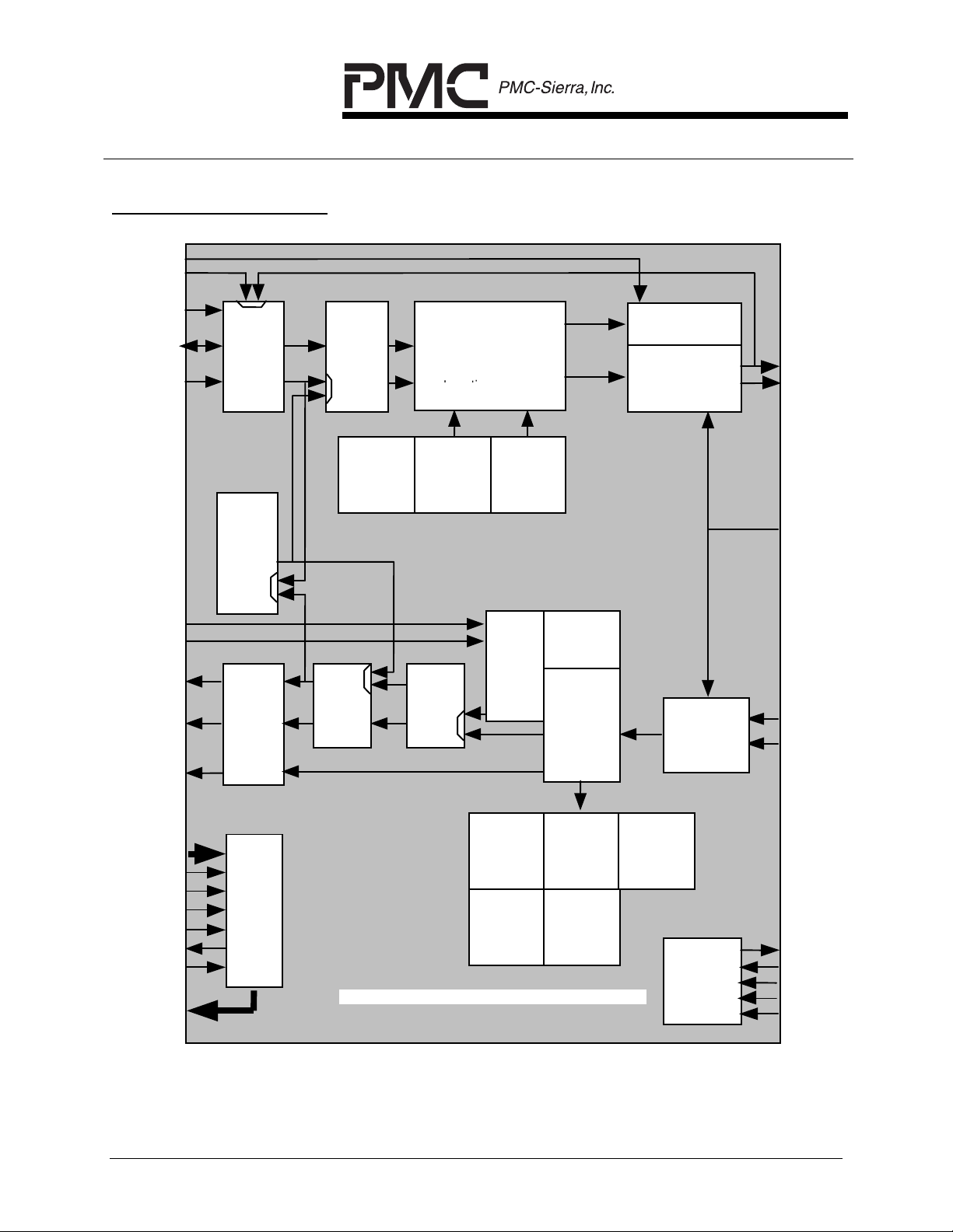
BLOCK DIAGRAM
EIF
Egress
Interface
PRGD
Pattern
Generator/
Detector
IIF
Ingress
Interface
TPSC
Per-DS0
Controller
Transmitter
RPSC
Per-DS0
Controller
TDPR
HDLC
TRANSMITTER
XBAS
BasicTransmitter:
Frame Generation,
Alarm Insertion,
Signaling
Trunk Conditioning
XBOC
Bit Oriented
Code
Generator
RECEIVER
SIGX
Signaling
Extractor
ELST
Elastic
XIBC
Inband
Loopback
Code
Generator
ELST
Elastic
Store
Store
FRAM
Framer/
Elastic Store
RAM
FRMR
Framer:
Frame
Alignment,
Alarm
Extraction
TOPS
Timing Options
TJAT
Digital Jitter
Attenuator
RJAT
Digital Jitter
Attenuator
TLCLK[1:8]
TLD[1:8]
XCLK*
RLCLK[1:
RLD[1:8]
IFP[1:8]
RBOC
A[10:0]*
RDB*
WRB*
CSB*
ALE*
INTB*
RSTB*
D[7:0]*
PROPRIETARY AND CONFIDENTIAL TO PMC-SIERRA, INC., AND FOR ITS CUSTOMERS’ INTERNAL USE
MPIF
Micro-
Processor
Interface
* These signals are shared between all eight framers.
Bit Oriented
Code
Detector
RDLC
HDLC
Receiver
ALMI
Alarm
Integrator
PMON
Performance
Monitor
Counters
IBCD
Inband
Loopback
Code
Detector
Test Access
JTAG
Port
TDO
TDI
TCLK
TMS
TRSTB
6
Page 23

PM4388 TOC TL
DATA SHEET
PMC-960840 ISSUE 5 OCTAL T1 FRAMER
6
DESCRIPTION
The PM4388 Octal T1 Framer (TOCTL) is a feature-rich device for use primarily
in systems carrying data (frame relay, Point to Point Protocol, or other protocols)
over DS-1 facilities. Each of the framers and transmitters is independently
software configurable, allowing feature selection without changes to external
wiring.
On the receive side, each of eight independent framers can be configured to
frame to either of the common DS-1 signal formats: (SF, ESF) or to be bypassed
(unframed mode). The TOCTL detects and indicates the presence of Yellow and
AIS patterns and also integrates Yellow, Red, and AIS alarms.
Performance monitoring with accumulation of CRC-6 errors, framing bit errors,
out-of-frame events, and changes of frame alignment is provided. The TOCTL
also detects the presence of in-band loopback codes, ESF bit oriented codes,
and detects and terminates HDLC messages on the ESF data link. The HDLC
messages are terminated in a 128 byte FIFO. An elastic store that optionally
supports slip buffering and adaptation to backplane timing is provided, as is a
signaling extractor that supports signaling debounce, signaling freezing and
interrupt on signaling state change on a per-DS0 basis. The TOCTL also
supports idle code substitution and detection, digital milliwatt code insertion, data
extraction, trunk conditioning, data sign and magnitude inversion, and pattern
generation or detection on a per-DS0 basis.
On the transmit side, the TOCTL generates framing for SF or ESF DS-1 formats,
or framing can be optionally disabled. The TOCTL supports signaling insertion,
idle code substitution, data insertion, line loopback, data inversion, zero-code
suppression, and pattern generation or detection on a per-DS0 basis.
The TOCTL can generate a low jitter transmit clock from a variety of clock
references, and also provides jitter attenuation in the receive path.
The TOCTL provides a parallel microprocessor interface for controlling the
operation of the TOCTL device. Serial PCM interfaces allow 1.544 Mbit/s
ingress/egress system interfaces to be directly supported. Tolerance of gapped
clocks allows other backplane rates to be supported with a minimum of external
logic.
It should be noted that the TOCTL device operates on unipolar data only: B8ZS
substitution and line code violation monitoring, if required, must be processed by
the T1 LIU.
PROPRIETARY AND CONFIDENTIAL TO PMC-SIERRA, INC., AND FOR ITS CUSTOMERS’ INTERNAL USE
7
Page 24
PM4388 TOC TL
DATA SHEET
PMC-960840 ISSUE 5 OCTAL T1 FRAMER
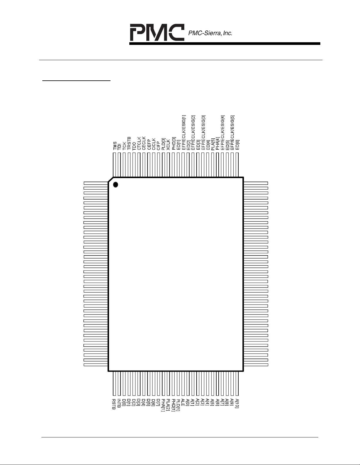
7
PIN DIAGRAM
The TOCTL is packaged in a 128-pin plastic QFP package having a body size of
14mm by 20mm and a pin pitch of 0.5mm.
PIN 128
PIN 1
RLD[1]
RLCLK[1]
RLD[2]
RLCLK[2]
RLD[3]
RLCLK[3]
RLD[4]
RLCLK[4]
TLD[1]
TLCLK[1]
TLD[2]
TLCLK[2]
TLD[3]
TLCLK[3]
TLD[4]
TLCLK[4]
BIAS
PHA[0]
PLA[0]
PHD[0]
PLD[0]
TLD[5]
TLCLK[5]
TLD[6]
TLCLK[6]
TLD[7]
TLCLK[7]
TLD[8]
TLCLK[8]
PLA[1]
RLD[5]
RLCLK[5]
RLD[6]
RLCLK[6]
RLD[7]
RLCLK[7]
RLD[8]
RLCLK[8]
Index Pin
PM 4388
TOC TL
Top
View
PIN 103
PIN 102
EFP/ECLK/ESIG[6]
ED[7]
EFP/ECLK/ESIG[7]
ED[8]
EFP/ECLK/ESIG[8]
ID[1]
ICLK/ISIG[1]
IFP[1]
ID[2]
PLA[4]
PHA[3]
ICLK/ISIG[2]
IFP[2]
ID[3]
ICLK/ISIG[3]
IFP[3]
PLD[2]
PHD[2]
ID[4]
ICLK/ISIG[4]
IFP[4]
ID[5]
ICLK/ISIG[5]
IFP[5]
ID[6]
ICLK/ISIG[6]
IFP[6]
PLA[3]
PHA[2]
ID[7]
ICLK/ISIG[7]
IFP[7]
ID[8]
ICLK/ISIG[8]
IFP[8]
RDB
WRB
CSB
PIN 38
PIN 39 PIN 64
PROPRIETARY AND CONFIDENTIAL TO PMC-SIERRA, INC., AND FOR ITS CUSTOMERS’ INTERNAL USE
PIN 65
8
Page 25

PM4388 TOC TL
[7]ED[6]
[4]
]
[1]
]
[1]ED[8]
[6]ED[5]
[2]ED[1]
[2]
]
[2]
[1]
[8]
[7]
]
[3]
]
[2]
]
[5]ED[4]ED[2]
]
[3]
]
]
[4]
]
]
[4]
]ID[6]
]
]
[5]
[5]
]
[7]
]
[6]ID[7]
]A[9]A[7]
]
]
[2]ID[8]
]A[3]A[0]D[5]D[2]
]
[7]
]A[4]A[1]
]D[0]
]
[8]
]A[5]A[2]
]D[3]D[1]
]
DATA SHEET
PMC-960840 ISSUE 5 OCTAL T1 FRAMER
The TOCTL is also available in a 128 pin Chip Array Ball Grid Array (CABGA)
package having a body size of 11mm by 11mm and a ball pitch of 0.8mm.
121110987654321
A
ED
B
ID
C
ID
ICLK/
D
ISIG
ICLK/
E
ISIG
F
ID
ICLK/
ISIG
IFP[2]PHA[3]IFP[1
IFP[3]ID[3]PLA[4
PHD[2]PLD[2]ID[5
EFP/
ECLK/
ESIG
EFP/
ECLK/
ESIG
EFP/
ECLK/
ESIG
PLA[5]ED[3
EFP/
ECLK/
ESIG
EFP/
ECLK/
ESIG
PHA[4
EFP/
ECLK/
ESIG
EFP/
ECLK/
ESIG
EFP/
ECLK/
ESIG
PHD[3]CICLK CTCLK TCK RLD[1]RLD[3
XCLK/
VCLK
PLD[3]CEFP TDO RLCLK[1]RLCLK[3]TLCLK[1
CIFP CECLK TMS RLD
TRSTB TDI RLCLK[2]TLD[1]TLCLK[2
RLCLK[4]TLD[2]TLCLK[4]TLD[4
TLD[3]TLCLK[3]PLA[0]PHA[0
RLD[4
A
B
C
D
E
F
BOTTOM VIEW
G
IFP
H
IFP
J
IFP
K
PHA
ICLK/
ISIG[4
ICLK/
ISIG
PLA[3
IFP[8
WRB A[6
ICLK/
ISIG[6
ICLK/
ISIG
PHA[1]D[4
BIAS TLD[5]PLD[0]PHD[0
TLCLK[8]TLCLK[6]TLCLK[5]TLD[6
INTB RLD[5]TLD[8]TLD[7]TLCLK[7
RLCLK[7]RLCLK[6]RLCLK[5]PLA[1
G
H
J
K
L
IFP
ICLK/
M
ISIG
121110987654321
PROPRIETARY AND CONFIDENTIAL TO PMC-SIERRA, INC., AND FOR ITS CUSTOMERS’ INTERNAL USE
RDB A[10
CSB A[8
ALE PHD[1]D[7
PLD[1]PLA[2]D[6
RLCLK[8]RLD[7]RLD[6
RSTB RLD[8
9
L
M
Page 26

PM4388 TOC TL
DATA SHEET
PMC-960840 ISSUE 5 OCTAL T1 FRAMER
8
PIN DESCRIPTION
Pin
Name
RLD[1]
RLD[2]
RLD[3]
RLD[4]
RLD[5]
RLD[6]
RLD[7]
RLD[8]
RLCLK[1]
RLCLK[2]
RLCLK[3]
RLCLK[4]
RLCLK[5]
RLCLK[6]
RLCLK[7]
RLCLK[8]
Type Pin No.
-RI -NI
Input 1
3
5
7
31
33
35
37
Input 2
4
6
8
32
34
36
38
A2
B2
A1
B1
J4
L1
L2
M1
C3
D3
C2
E4
K2
K3
K4
L3
Function
Receive Line Data (RLD[1:8]). RLD[1:8]
contain the receive stream from each of the
eight DS-1 line interface units, or from a higher
order demultiplex interface. These inputs are
sampled on the active edge of the
corresponding RLCLK[1:8].
Receive Line Clocks (RLCLK[1:8]). Each input
is an externally recovered 1.544 MHz line clock
that samples the RLD[x] inputs on its active
edge. RLCLK[x] may be a gapped clock
subject to the timing constraints in the AC
Timing section of this datasheet.
PROPRIETARY AND CONFIDENTIAL TO PMC-SIERRA, INC., AND FOR ITS CUSTOMERS’ INTERNAL USE
10
Page 27

PM4388 TOC TL
DATA SHEET
PMC-960840 ISSUE 5 OCTAL T1 FRAMER
Pin
Name
ICLK[1]
ICLK[2]
ICLK[3]
ICLK[4]
ICLK[5]
ICLK[6]
ICLK[7]
ICLK[8]/
ISIG[1]
ISIG[2]
ISIG[3]
ISIG[4]
ISIG[5]
ISIG[6]
ISIG[7]
ISIG[8]
Type Pin No.
-RI -NI
Output 96
91
88
83
80
77
72
69
C11
D12
E12
G11
H11
G9
H9
M12
Function
Ingress Clocks (ICLK[1:8]). The Ingress Clocks
are active when the external signaling interface
is disabled. Each ingress clock is a smoothed
(jitter attenuated) version of the associated
receive line clock (RLCLK[x]). When the Clock
Master: NxDS0 mode is active, ICLK[x] is a
gapped version of the smoothed RLCLK[x].
When Clock Slave: ICLK Reference mode is
active, ICLK[x] may optionally be the smoothed
RLCLK[x], or the smoothed RLCLK[x] divided
by 193. When Clock Master: Full DS1 mode is
active, IFP[x] and ID[x] are updated on the
active edge of ICLK[x]. When the Clock
Master: NxDS0 mode is active, ID[x] is updated
on the active edge of ICLK[x].
Ingress Signaling (ISIG[1:8]). When the Clock
Slave: External Signaling mode is enabled,
each ISIG[x] contains the extracted signaling
bits for each channel in the frame, repeated for
the entire superframe. Each channel's
signaling bits are valid in bit locations 5,6,7,8
of the channel and are channel-aligned with
the ID[x] data stream. ISIG[x] is updated on
the active edge of the common ingress clock,
CICLK.
IFP[1]
IFP[2]
IFP[3]
IFP[4]
IFP[5]
IFP[6]
IFP[7]
IFP[8]
Output 95
90
87
82
79
76
71
68
D9
D11
E11
G12
H12
J12
L12
J10
Ingress Frame Pulse (IFP[1:8]). The IFP[x]
outputs are intended as timing references.
IFP[x] indicates the frame alignment or the
superframe alignment of the ingress stream,
ID[x].
When Clock Master: Full DS1 mode is active,
IFP[x] is updated on the active edge of the
associated ICLK[x]. When Clock Master:
NxDS0 mode is active, ICLK[x] is gapped
during the pulse on IFP[x]. When the Clock
Slave ingress modes are active, IFP[x] is
updated on the active edge of CICLK.
PROPRIETARY AND CONFIDENTIAL TO PMC-SIERRA, INC., AND FOR ITS CUSTOMERS’ INTERNAL USE
11
Page 28

PM4388 TOC TL
DATA SHEET
PMC-960840 ISSUE 5 OCTAL T1 FRAMER
Pin
Name
ID[1]
ID[2]
ID[3]
ID[4]
ID[5]
ID[6]
ID[7]
ID[8]
Type Pin No.
-RI -NI
Output 97
94
89
84
81
78
73
70
B12
C12
E10
F12
F9
G10
J11
K11
Function
Ingress Data (ID[1:8]). Each ID[x] signal
contains the recovered data stream which may
have been passed through the elastic store.
When the Clock Slave ingress modes are
active, the ID[x] stream is aligned to the
common ingress timing and is updated on the
active edge of CICLK.
When the Clock Master ingress modes are
active, ID[x] is aligned to the receive line timing
and is updated on the active edge of the
associated ICLK[x].
CICLK Input 120 A5 Common Ingress Clock (CICLK). CICLK is
either a 1.544MHz or 2.048MHz clock with
optional gapping for adaptation to non-uniform
backplane data streams. CICLK is common to
all eight framers. CIFP is sampled on the
active edge of CICLK. When the Clock Slave
ingress modes are active, ID[x], ISIG[x], and
IFP[x] are updated on the active edge of
CICLK.
CIFP Input 119 B5 Common Ingress Frame Pulse (CIFP). When
the elastic store is enabled (Clock Slave mode
is active on the ingress side), CIFP is used to
frame align the ingress data to the system
frame alignment. CIFP is common to all eight
framers. When frame alignment is required, a
pulse at least 1 CICLK cycle wide must be
provided on CIFP a maximum of once every
frame (nominally 193 bit times or 256 bit times
if the 2.048 MHz rate is selected). If ingress
signaling alignment is required, ingress
signaling alignment must be enabled, and a
pulse at least 1 CICLK cycle wide must be
provided on CIFP every 12 or 24 frame times.
CIFP is sampled on the active edge of CICLK.
PROPRIETARY AND CONFIDENTIAL TO PMC-SIERRA, INC., AND FOR ITS CUSTOMERS’ INTERNAL USE
12
Page 29

PM4388 TOC TL
DATA SHEET
PMC-960840 ISSUE 5 OCTAL T1 FRAMER
Pin
Name
ED[1]
ED[2]
ED[3]
ED[4]
ED[5]
ED[6]
ED[7]
ED[8]
EFP[1]
EFP[2]
EFP[3]
EFP[4]
EFP[5]
EFP[6]
EFP[7]
EFP[8]/
Type Pin No.
-RI -NI
Input 115
113
111
109
105
103
101
99
I/O 114
112
110
106
104
102
100
98
B7
D6
A8
D7
B9
A11
A12
B11
A7
B8
C7
A10
D8
B10
C9
C10
Function
Egress Data (ED[1:8]). The egress data
streams to be transmitted are input on these
pins. When the Clock Master: Full DS1 mode
is active, ED[x] is sampled on the rising edge
of TLCLK[x]. When the Clock Master: NxDS0
mode is active, ED[x] is sampled on the active
edge of ECLK[x]. When the Clock Slave
egress modes are active, ED[x] is sampled on
the active edge of CECLK.
Egress Frame Pulse (EFP[1:8]). When the
Clock Master: Full DS1 or Clock Slave: EFP
Enabled modes are active, the EFP[1:8]
outputs indicate the frame alignment or the
superframe alignment of each of the eight
framers. When the Clock Master modes are
active, EFP[x] is updated by the falling edge of
the TLCLK[x]. When the Clock Slave egress
modes are active, EFP[x] is updated on the
active edge of CECLK.
ECLK[1]
ECLK[2]
ECLK[3]
ECLK[4]
ECLK[5]
ECLK[6]
ECLK[7]
ECLK[8]
ESIG[1]
ESIG[2]
ESIG[3]
ESIG[4]
ESIG[5]
ESIG[6]
ESIG[7]
ESIG[8]
Egress Clock (ECLK[1:8]). When the Clock
Master: NxDS0 mode is active, the ECLK[x]
output is used to sample the associated egress
data (ED[x]). ECLK[x] is a version of TLCLK[x]
that is gapped during the framing bit position
and optionally for between 1 and 23 DS0
channels in the associated ED[x] stream.
ED[x] is sampled on the active edge of the
associated ECLK[x].
Egress Signaling (ESIG[1:8]). When the Clock
Slave: External Signaling mode is active, the
ESIG[8:1] inputs contain the signaling bits for
each channel in the transmit data frame,
repeated for the entire superframe. Each
channel's signaling bits are in bit locations
5,6,7,8 of the channel and are frame-aligned
by the common egress frame pulse, CEFP.
ESIG[x] is sampled on the active edge of
CECLK.
PROPRIETARY AND CONFIDENTIAL TO PMC-SIERRA, INC., AND FOR ITS CUSTOMERS’ INTERNAL USE
13
Page 30

PM4388 TOC TL
DATA SHEET
PMC-960840 ISSUE 5 OCTAL T1 FRAMER
Pin
Name
Type Pin No.
-RI -NI
Function
CTCLK Input 123 A4 Common Transmit Clock (CTCLK). This input
signal is used to generate the TLCLK[x] clock
signals. Depending on the configuration of the
TOCTL, CTCLK may be a 12.352 MHz clock
(so TLCLK[x] is generated by dividing CTCLK
by 8), or a line rate clock (so TLCLK[x] is
generated directly from CTCLK, or from
CTCLK after jitter attenuation), or a multiple of
8kHz (Nx8khz, where 1•N•256) so long as
CTCLK is jitter-free when divided down to
8kHz (in which case TLCLK is derived by the
DJAT PLL using CTCLK as a reference).
The TOCTL may be configured to ignore the
CTCLK input and utilize CECLK or RLCLK[x]
instead. RLCLK[x] is automatically substituted
for CTCLK if line loopback is enabled.
CECLK Input 122 B4 Common Egress Clock (CECLK). The
common egress clock is used to time the
egress interface when Clock Slave mode is
enabled in the egress side. CECLK may be a
1.544MHz or 2.048MHz clock with optional
gapping for adaptation from non-uniform
system clocks. When the Clock Slave: EFP
Enabled mode is active, CEFP and ED[x] are
sampled on the active edge of CECLK, and
EFP[x] is updated on the active edge of
CECLK. When the Clock Slave: External
Signaling mode is active, CEFP, ESIG[x] and
ED[x] are sampled on the active edge of
CECLK.
PROPRIETARY AND CONFIDENTIAL TO PMC-SIERRA, INC., AND FOR ITS CUSTOMERS’ INTERNAL USE
14
Page 31

PM4388 TOC TL
DATA SHEET
PMC-960840 ISSUE 5 OCTAL T1 FRAMER
Pin
Name
Type Pin No.
-RI -NI
Function
CEFP Input 121 C5 Common Egress Frame Pulse. CEFP may be
used to frame align the framers to the system
backplane. If frame alignment only is required,
a pulse at least 1 CECLK cycle wide must be
provided on CEFP every 193 bit times. If
superframe alignment is required, transmit
superframe alignment must be enabled, and a
pulse at least 1 CECLK cycle wide must be
provided on CEFP every 12 or 24 frame times,
on the last F-bit of the multiframe. CEFP is
sampled on the active edge of CECLK. CEFP
has no effect in the Clock Master egress
modes
TLCLK[1]
TLCLK[2]
TLCLK[3]
TLCLK[4]
TLCLK[5]
TLCLK[6]
TLCLK[7]
TLCLK[8]
Output 10
12
14
16
23
25
27
29
C1
D1
F3
E2
H2
H3
J1
H4
Transmit Line Clock (TLCLK[1:8]). The TLD[x]
outputs are updated on the active edge of the
associated TLCLK[x]. When the Clock Master:
Full DS1 mode is active, ED[1:8] is sampled on
the active edge of TLCLK[x] and EFP[1:8] is
updated on the active edge of TLCLK[x].
TLCLK[x] is a 1.544 MHz clock that is
adequately jitter and wander free in absolute
terms to permit an acceptable DS-1 signal to
be generated. Depending on the configuration
of the TOCTL, TLCLK[x] may be derived from
CTCLK, CECLK, or RLCLK[x], with or without
jitter attenuation.
TLD[1]
TLD[2]
TLD[3]
TLD[4]
TLD[5]
TLD[6]
TLD[7]
TLD[8]
PROPRIETARY AND CONFIDENTIAL TO PMC-SIERRA, INC., AND FOR ITS CUSTOMERS’ INTERNAL USE
Output 9
11
13
15
22
24
26
28
D2
E3
F4
E1
G3
H1
J2
J3
Transmit Line Data (TLD[1:8]). TLD[1:8]
contain the transmit stream for each of the
eight DS-1 line interface units, or for the higher
order multiplex interface. These outputs are
updated on the active edge of the
corresponding TLCLK[1:8].
15
Page 32

PM4388 TOC TL
DATA SHEET
PMC-960840 ISSUE 5 OCTAL T1 FRAMER
Pin
Name
Type Pin No.
-RI -NI
Function
XCLK/ Input 117 B6 Crystal Clock Input (XCLK). This signal
provides timing for many portions of the
TOCTL. XCLK is nominally a 37.056 MHz ±
32ppm, 50% duty cycle clock.
VCLK Vector Clock (VCLK). The VCLK signal is used
during TOCTL production test to ver ify internal
functionality.
INTB Output 40 J5 Active low open-drain Interrupt signal (INTB).
This signal goes low when an unmasked
interrupt event is detected on any of the
internal interrupt sources. Note that INTB will
remain low until all active, unmasked interrupt
sources are acknowledged at their source.
CSB Input 65 M11 Active low chip select (CSB). This signal must
be low to enable TOCTL register accesses.
CSB must go high at least once after a
powerup to clear internal test modes. If CSB is
not used, then it should be tied to an inverted
version of RSTB, in which case, RDB and
WRB determine register accesses.
D[0]
D[1]
D[2]
D[3]
D[4]
D[5]
D[6]
D[7]
I/O 41
42
43
44
45
46
47
48
L4
M3
K5
M4
J6
K6
M5
L5
Bidirectional data bus (D[7:0]). This bus is used
during TOCTL read and write accesses.
RDB Input 67 L11 Active low read enable (RDB). This signal is
pulsed low to enable a TOCTL register read
access. The TOCTL drives the D[7:0] bus with
the contents of the addressed register while
RDB and CSB are both low.
PROPRIETARY AND CONFIDENTIAL TO PMC-SIERRA, INC., AND FOR ITS CUSTOMERS’ INTERNAL USE
16
Page 33

PM4388 TOC TL
DATA SHEET
PMC-960840 ISSUE 5 OCTAL T1 FRAMER
Pin
Name
Type Pin No.
-RI -NI
Function
WRB Input 66 K10 Active low write strobe (WRB). This signal is
pulsed low to enable a TOCTL register write
access. The D[7:0] bus contents are clocked
into the addressed normal mode register on
the rising edge of WRB while CSB is low.
ALE Input 53 L7 Address latch enable (ALE). This signal latches
the address bus contents, A[10:0], when low,
allowing the TOCTL to be interfaced to a
multiplexed address/data bus. When ALE is
high, the address latches are transparent. ALE
has an integral pull-up.
RSTB Input 39 M2 Active low reset (RSTB). This signal is set low
to asynchronously reset the TOCTL. RSTB is
a Schmitt-trigger input with integral pull-up.
When resetting the device, RSTB must be
asserted for a minimum of 100 ns to ensure
that the TOCTL is completely reset.
A[0]
A[1]
A[2]
A[3]
A[4]
A[5]
A[6]
A[7]
A[8]
A[9]
A[10]
Input 54
55
56
57
58
59
60
61
62
63
64
K7
L8
M8
K8
L9
M9
K9
J8
M10
J9
L10
Address bus (A[10:0]). This bus selects specific
registers during TOCTL register accesses.
TCK Input 126 A3 Test Clock (TCK).The test clock (TCK) signal
provides timing for test operations that can be
carried out using the IEEE P1149.1 test
access port.
TMS Input 128 B3 Test Mode Select (TMS). The test mode select
(TMS) signal controls the test operations that
can be carried out using the IEEE P1149.1 test
access port. TMS is sampled on the rising
edge of TCK. TMS has an integral pull up
resistor.
PROPRIETARY AND CONFIDENTIAL TO PMC-SIERRA, INC., AND FOR ITS CUSTOMERS’ INTERNAL USE
17
Page 34

PM4388 TOC TL
DATA SHEET
PMC-960840 ISSUE 5 OCTAL T1 FRAMER
Pin
Name
Type Pin No.
-RI -NI
Function
TDI Input 127 D4 Test Input (TDI).The test data input (TDI) signal
carries test data into the TOCTL via the IEEE
P1149.1 test access port. TDI is sampled on
the rising edge of TCK. TDI has an integral
pull up resistor.
TDO Tristate 124 C4 Test Output (TDO).The test data output (TDO)
signal carries test data out of the TOCTL via
the IEEE P1149.1 test access port. TDO is
updated on the falling edge of TCK. TDO is a
tristate output which is tristated except when
scanning of data is in progress.
TRSTB Input 125 D5 Test Reset (TRSTB).The active low test reset
(TRSTB) signal provides an asynchronous
TOCTL test access port reset via the IEEE
P1149.1 test access port. TRSTB is a Schmitt
triggered input with an integral pull up resistor.
The JTAG TAP controller must be initialized
when the TOCTL is powered up. If the JTAG
port is not used TRSTB must be connected to
the RSTB input or grounded.
BIAS Input 17 G4 +5V Bias (BIAS). The BIAS input is used to
implement 5V tolerance on the inputs. BIAS
must be connected to a well decoupled +5V
rail if 5V tolerant inputs are required. If 5V
tolerant inputs are not required, BIAS must be
connected to a well-decoupled 3.3V DC supply
together with the power pins PHA[3:0] and
PHD[3:0].
PHA[0]
PHA[1]
PHA[2]
PHA[3]
PHA[4]
PHD[0]
PHD[1]
PHD[2]
PHD[3]
PROPRIETARY AND CONFIDENTIAL TO PMC-SIERRA, INC., AND FOR ITS CUSTOMERS’ INTERNAL USE
Power 18
49
74
92
107
Power 20
51
85
116
F1
J7
K12
D10
C8
G1
L6
F11
A6
Pad ring power pins (PHA[4:0]). These pins
must be connected to a common, well
decoupled +3.3V DC supply together with the
core power pins PHD3:0] .
Core power pins (PHD[3:0]). These pins must
be connected to a common, well decoupled
+3.3V DC supply together with the pad ring
power pins PHA[4:0].
18
Page 35

PM4388 TOC TL
DATA SHEET
PMC-960840 ISSUE 5 OCTAL T1 FRAMER
Pin
Name
PLA[0]
PLA[1]
PLA[2]
PLA[3]
PLA[4]
PLA[5]
PLD[0]
PLD[1]
PLD[2]
PLD[3]
Type Pin No.
-RI -NI
Ground 19
30
50
75
93
108
Ground 21
52
86
118
F2
K1
M6
H10
E9
A9
G2
M7
F10
C6
Function
Pad ring ground pins (PLA[5:0]). These pins
must be connected to a common ground
together with the core ground pins PLD[3:0].
Core ground pins (PLD[3:0]). These pins must
be connected to a common ground together
with the pad ring ground pins PLA[5:0].
Notes on Pin Description:
1. The PLA[5:0] and PLD[3:0] ground pins are not internally connected together.
Failure to connect these pins externally may cause malfunction or damage
the device. The PHA[4:0] and PHD[3:0] power pins are not internally
connected together. Failure to connect these pins externally may cause
malfunction or damage the device. These power supply connections must all
be utilized and must all connect to a common +3.3 V or ground rail, as
appropriate.
2. During power-up, and power-down the voltage on the BIAS pin must be kept
equal to or greater than the voltage on the PHA[4:0] and PHD[3:0] pins, to
avoid damage to the device.
3. Inputs RSTB, TMS, TDI, and ALE have integral pull-up resistors.
4. All outputs have 2 mA drive capability except for the D[7:0] bidirectionals and
the TLCLK[8:1], ECLK[8:1], and ICLK[8:1] clock outputs which have 3 mA
drive capability.
5. All inputs and bidirectionals present minimum capacitive loading.
6. Certain inputs are described as being sampled by the "active edge" of a
particular clock. These inputs may be enabled to be sampled on either the
rising edge or the falling edge of that clock, depending on the software
configuration of the device.
PROPRIETARY AND CONFIDENTIAL TO PMC-SIERRA, INC., AND FOR ITS CUSTOMERS’ INTERNAL USE
19
Page 36

PM4388 TOC TL
DATA SHEET
PMC-960840 ISSUE 5 OCTAL T1 FRAMER
9
FUNCTIONAL DESCRIPTION
9.1 Framer (FRMR)
The framing function is provided by the FRMR block. This block searches for the
framing bit position in the ingress stream. It works in conjunction with the FRAM
block to search for the framing bit pattern in the standard superframe (SF), or
extended superframe (ESF) framing formats. When searching for frame, the
FRMR simultaneously examines each of the 193 (SF) or each of the 772 (ESF)
framing bit candidates. The FRAM block is addressed and controlled by the
FRMR while frame synchronization is acquired.
The time required to acquire frame alignment to an error-free ingress stream,
containing randomly distributed channel data (i.e. each bit in the channel data
has a 50% probability of being 1 or 0), is dependent upon the framing format.
For SF format, the FRMR block will determine frame alignment within 4.4ms 99
times out of 100. For ESF format, the FRMR will determine frame alignment
within 15 ms 99 times out of 100.
Once the FRMR has found frame, the ingress data is continuously monitored for
framing bit errors, bit error events (a framing bit error in SF or a CRC-6 error in
ESF), and severely errored framing events. The FRMR also detects out-of-frame,
based on a selectable ratio of framing bit errors.
The FRMR can also be disabled to allow reception of unframed data. While the
FRMR is disabled, control of the FRAM block is relinquished for use as the
elastic store.
9.2 Framer/Slip Buffer RAM (FRAM)
The Framer/Slip Buffer RAM function is provided by the Framer RAM (FRAM)
block. The FRAM is used to store up to 4 frames of data while the FRMR is
acquiring frame and up to 2 frames of data during normal operation (i.e. when
accessed by Elastic Store). The FRAM is shared between the Elastic Store
(ELST) and the FRMR: when frame synchronization is lost, the FRMR takes
control of the FRAM and uses it to find frame; when frame synchronization is
determined, the FRMR relinquishes control of FRAM to ELST which buffers the
incoming PCM data.
PROPRIETARY AND CONFIDENTIAL TO PMC-SIERRA, INC., AND FOR ITS CUSTOMERS’ INTERNAL USE
20
Page 37

PM4388 TOC TL
DATA SHEET
PMC-960840 ISSUE 5 OCTAL T1 FRAMER
9.3 Inband Loopback Code Detector (IBCD)
The Inband Loopback Code Detection function is provided by the IBCD block.
This block detects the presence of either of two programmable INBAND
LOOPBACK ACTIVATE and DEACTIVATE code sequences in either framed or
unframed data streams. The inband code sequences are expected to be
overwritten by the framing bit in framed data streams. Each INBAND
LOOPBACK code sequence is defined as the repetition of the programmed code
in the ingress stream for at least 5.1 seconds. The code sequence detection and
timing is compatible with the specifications defined in T1.403, TA-TSY-000312,
and TR-TSY-000303. LOOPBACK ACTIVATE and DEACTIVATE code indication
is provided through internal register bits. An interr upt is generated to indicate
when either code status has changed.
If inband code detection is not desired, the IBCD_IDLE bit may be set in the
Receive Line Options register, allowing the IBCD to be used to detect the DS1
idle code in the receive stream. Setting the IBCD_IDLE bit gaps the data to the
IBCD block dur ing the frame bit so that the IBCD searches for the programmed
pattern in the payload.
9.4 Performance Monitor Counters (PMON)
The Performance Monitor Counters function is provided by the PMON block. The
block accumulates CRC error events, Frame Synchronization bit error events,
out-of-frame events, and Change of Frame Alignment (COFA) events with
saturating counters over consecutive intervals as defined by the time between
writes of the Revision/Chip ID/Global PMON update register (00CH), or every
second via the AUTOUPDATE feature in the Receive Line Options register, or by
writing to any of the PMON holding registers. The PMON uses a 12-bit counter
for Bit Error Events (CRC-6 failures in ESF o r framing bit erro rs in SF), a 9-bit
counter for framing bit errors, a 5-bit counter for OOF events, and a 3-bit counter
for Change of Frame Alignment events. When an update is initiated by any
means, the PMON in each framer transfers the counter values into holding
registers and resets the counters to begin accumulating events for the interval.
The counters are reset in such a manner that error events occurring during the
reset are not missed. The holding register addresses are contiguous to facilitate
polling operations.
9.5 Bit Oriented Code Detector (RBOC)
The Bit Oriented Code detection function is provided by the RBOC block. This
block detects the presence of 63 of the possible 64 bit oriented codes
transmitted in the Facility Data Link channel in ESF framing format, as defined in
PROPRIETARY AND CONFIDENTIAL TO PMC-SIERRA, INC., AND FOR ITS CUSTOMERS’ INTERNAL USE
21
Page 38

PM4388 TOC TL
DATA SHEET
PMC-960840 ISSUE 5 OCTAL T1 FRAMER
th
ANSI T1.403 and in TR-TSY-000194. The 64
code (111111) is similar to the
HDLC flag sequence and is used by the RBOC to indicate no valid code
received.
Bit oriented codes are received on the Facility Data Link channel as a 16-bit
sequence consisting of 8 ones, a zero, 6 code bits, and a trailing zero
(111111110xxxxxx0) which is repeated at least 10 times. The RBOC can be
enabled to declare a received code valid if it has been observed for 8 out of 10
times or for 4 out of 5 times, as specified by the AVC bit in the control register.
Valid BOC are indicated through an internal status register. The BOC bits are set
to all ones (111111) if no valid code has been detected. An interrupt is
generated to signal when a detected code has been validated, or optionally,
when a valid code goes away (i.e. the BOC bits go to all ones).
9.6 RDLC Facility Data Link Receiver
The RDLC is a microprocessor peripheral used to receive HDLC frames on the
4kHz ESF facility data link.
The RDLC detects the change from flag characters to the first byte of data,
removes stuffed zeros on the incoming data stream, receives packet data, and
calculates the CRC-CCITT frame check sequence (FCS).
In the address matching mode, only those packets whose first data byte matches
one of two programmable bytes or the universal address (all ones) are stored in
the FIFO. The two least significant bits of the address comparison can be
masked for LAPD SAPI matching.
Received data is placed into a 128-level FIFO buffer. An interrupt is generated
when a programmable number of bytes are stored in the FIFO buffer. Other
sources of interrupt are detection of the terminating flag sequence, abort
sequence, or FIFO buffer overrun.
The Status Register contains bits which indicate the overrun or empty FIFO
status, the interrupt status, and the occurrence of first flag or end of message
bytes written into the FIFO. The Status Register also indicates the abort, flag,
and end of message status of the data just read from the FIFO. On end of
message, the Status Register indicates the FCS status and if the packet
contained a non-integer number of bytes.
PROPRIETARY AND CONFIDENTIAL TO PMC-SIERRA, INC., AND FOR ITS CUSTOMERS’ INTERNAL USE
22
Page 39

PM4388 TOC TL
DATA SHEET
PMC-960840 ISSUE 5 OCTAL T1 FRAMER
9.7 Alarm Integrator (ALMI)
The Alarm Integration function is provided by the ALMI block. This block detects
the presence of Yellow, Red, and AIS Carrier Fail Alarms (CFA) in SF, or ESF
formats. The alarm detection and integration is compatible with the specifications
defined in ANSI T1.403 and TR-TSY-000191.
The ALMI block declares the presence of Yellow alar m when the Yellow pattern
has been received for 425 ms (± 50 ms); the Yellow alarm is removed when the
Yellow pattern has been absent for 425 ms (± 50 ms). The presence of Red
alarm is declared when an out-of-frame condition has been present for 2.55 sec
(± 40 ms); the Red alarm is removed when the out-of-frame condition has been
absent for 16.6 sec (± 500 ms). The presence of AIS alarm is declared when an
out-of-frame condition and all-ones in the PCM data stream have been present
for 1.5 sec (±100 ms); the AIS alarm is removed when the AIS condition has
been absent for 16.8 sec (±500 ms).
CFA alarm detection algorithms operate in the presence of a 10-3 bit error rate.
The ALMI also indicates the presence or absence of the Yellow, Red, and AIS
alarm signal conditions over 40 ms, 40 ms, and 60 ms intervals, respectively,
allowing an external microprocessor to integrate the alarm conditions via
software with any user-specific algorithms. Alarm indication is provided through
internal register bits.
9.8 Elastic Store (ELST)
The Elastic Store (ELST) synchronizes ingress frames to the common ingress
clock and frame pulse (CICLK, CIFP) in the Clock Slave ingress modes. The
frame data is buffered in a two frame circular data buffer. Input data is written to
the buffer using a write pointer and output data is read from the buffer using a
read pointer.
The elastic store can be bypassed to eliminate the 2 frame delay. In this
configuration (the Clock Master ingress modes), the elastic store is used to
synchronize the ingress frames to the transmit line clock (TLCLK[x]) so that perDS0 loopbacks may be enabled. Per-DS0 loopbacks are only available when the
elastic store is bypassed, or when CECLK and CICLK are tied together and
CEFP and CIFP are tied together, and the CICLKRISE and CECLKFALL register
bits are either both logic 1 or both logic 0. CICLKRISE and CECLKFALL are
found in registers 3 and 4 of each octant, respectively.
PROPRIETARY AND CONFIDENTIAL TO PMC-SIERRA, INC., AND FOR ITS CUSTOMERS’ INTERNAL USE
23
Page 40

PM4388 TOC TL
DATA SHEET
PMC-960840 ISSUE 5 OCTAL T1 FRAMER
When the elastic store is being used, if the average frequency of the incoming
data is greater than the average frequency of the backplane clock, the write
pointer will catch up to the read pointer and the buffer will be filled. Under this
condition a controlled slip will occur when the read pointer crosses the next
frame boundary. The subsequent ingress frame is deleted.
If the average frequency of the incoming data is less than the average frequency
of the backplane clock, the read pointer will catch up to the write pointer and the
buffer will be empty. Under this condition a controlled slip will occur when the
read pointer crosses the next frame boundary. The previous ingress frame is
repeated.
A slip operation is always performed on a frame boundary.
For payload conditioning, the ELST inserts a programmable idle code into all
channels when the FRMR is out of frame synchronization. If the data is required
to pass through the TOCTL unchanged during an out-of-frame condition, then
the elastic store may be bypassed.
9.9 Signaling Extractor (SIGX)
The Signaling Extraction (SIGX) block provides signaling bit extraction from the
ingress stream for ESF, and SF framing formats. When the external signaling
interface is enabled, the SIGX serializes the bits into a serial stream aligned to
the synchronized outgoing data stream. The signaling data stream contains the
A,B,C,D bits in the lower 4 channel bit locations (bits 5,6,7,8) in ESF framing
format. In SF format, the A and B bits are repeated in locations C and D (i.e. the
signaling stream contains the bits ABAB for each channel). The SIGX also
provides user control over signaling freezing and provides control over signaling
bit fixing and signaling debounce on a per-DS0 basis. The block contains three
superframes worth of signal buffer ing to ensure that there is a greater than 95%
probability that the signaling bits are frozen in the correct state for a 50% ones
density out-of-frame condition, as specified in TR-TSY-000170 and BELL PUB
43801. With signaling debounce enabled, the per-DS0 signaling state must be in
the same state for 2 superframes before appearing on the serial output stream.
The SIGX indicates the occurrence of a change of signaling state for each DS0
via an interrupt and by a change of signaling state bit for each DS0.
9.10 Receive Per-DS0 Serial Controller (RPSC)
The RPSC allows data and signaling trunk conditioning to be applied on the
receive DS-1 stream on a per-DS0 basis. It also allows per-DS0 control of data
inversion, the extraction of clock and data on ICLK[x] and ID[x] (when the Clock
PROPRIETARY AND CONFIDENTIAL TO PMC-SIERRA, INC., AND FOR ITS CUSTOMERS’ INTERNAL USE
24
Page 41

PM4388 TOC TL
[x]
DATA SHEET
PMC-960840 ISSUE 5 OCTAL T1 FRAMER
Master: NxDS0 mode is active), and the detection or generation of pseudorandom or repetitive patterns. The RPSC operates on the data after its passage
through ELST, so that data and signaling conditioning may overwrite the ELST
trouble code.
9.11 Ingress Interface (IIF)
The Ingress Interface allows ingress data to be presented to a system using one
of four possible modes as selected by the IMODE[1:0] bits in the Ingress
Interface Options Register (Register 001H, 081H, 101H, 181H, 201H, 281H,
301H, 381H): Clock Master: Full DS1, Clock Master : NxDS0, Clock Slave : ICLK
Reference, or Clock Slave: External Signaling.
Figure 2 - Clock Master: Full DS1
FRAM
Framer/
Slip Buffer
ID[1:8]
IFP[1:8]
ID[x], IFP[x]
Timed to
ICLK
IIF
Ingress
Interface
RAM
FRMR
Framer:
Frame
Alignment,
Alarm
Extraction
RJAT
Digital Jitter
Attenuator
RLCLK[1:8]
RLD[1:8]
ICLK[1:8]
RECEIVER
In Clock Master: Full DS1 mode, the elastic store is bypassed and the ingress
clock (ICLK[x]) is a jitter attenuated version of the 1.544 MHz receive line clock
(RLCLK[x]). ICLK[x] is pulsed for each bit in the 193 bit frame. The ingress data
appears on ID[x] and the ingress frame alignment is indicated by IFP[x]. In this
mode, data passes through the TOCTL unchanged during out-of-frame
conditions, similar to an offline framer system. When the TOCTL is the clock
master in the ingress direction, then the elastic store is used to buffer between
the ingress and egress clocks to facilitate per-DS0 loopback.
PROPRIETARY AND CONFIDENTIAL TO PMC-SIERRA, INC., AND FOR ITS CUSTOMERS’ INTERNAL USE
25
Page 42

PM4388 TOC TL
8
g
]
DATA SHEET
PMC-960840 ISSUE 5 OCTAL T1 FRAMER
Figure 3 - Clock Master: NxDS0
FRAM
Framer/
Slip Buffer
ID[1:8]
IFP[1:8]
ID[x], IFP[x]
Timed to
apped ICLK[x
IIF
Ingress
Interface
RAM
FRMR
Framer:
Frame
Alignment,
Alarm
Extraction
RJAT
Digital Jitter
Attenuator
RLCLK[1:
RLD[1:8]
ICLK[1:8]
In this mode, ICLK[x] is derived from RLCLK[x], and is gapped on a per DS0
basis so that a subset of the 24 channels in the T1 frame is extracted on ID[x].
Channel extraction is controlled by the RPSC block. The framing bit position is
always gapped, so the number of ICLK[x] pulses is controllable from 0 to 192
pulses per frame on a per-DS0 basis. In this mode, data passes through the
TOCTL unchanged during out-of-frame conditions. The parity functions are not
usable in NxDS0 mode. When the TOCTL is the clock master in the ingress
direction, then the elastic store is used to buffer between the ingress and egress
clocks to facilitate per-DS0 loopback.
Figure 4 - Clock Slave: ICLK Reference
CICLK
CIFP
ID[1:8]
IFP[1:8]
ID[x], IFP[x]
Timed to CICLK[x]
IIF
Ingress
Interface
ELST
Elastic
Store
FRAM
Framer/
Slip Buffer
RAM
FRMR
Framer:
Frame
Alignment,
Alarm
Extraction
RJAT
Digital Jitter
Attenuator
RECEIVER
RLCLK[1:8]
RLD[1:8]
ICLK[1:8]
RECEIVER
In this mode, the elastic store is enabled to permit CICLK to specify the ingressside timing. The ingress data on ID[x] is bit aligned to the 1.544 MHz common
ingress clock (CICLK) and is frame aligned to the common ingress frame pulse
(CIFP). CICLK can be enabled to be a 1.544 MHz clock or a 2.048 MHz clock.
ICLK[x] can be enabled to be either a 1.544 MHz jitter attenuated version of
PROPRIETARY AND CONFIDENTIAL TO PMC-SIERRA, INC., AND FOR ITS CUSTOMERS’ INTERNAL USE
26
Page 43

PM4388 TOC TL
8
DATA SHEET
PMC-960840 ISSUE 5 OCTAL T1 FRAMER
RLCLK[x] or an 8 kHz version of RLCLK[x] (by dividing RLCLK[x] by 193). IFP[x]
indicates either the frame or superframe alignment on ID[x].
Figure 5 - Clock Slave: External Signaling
CICLK
CIFP
ID[1:8]
IFP[1:8]
ID[x], ISIG[x ],
IFP[x]
Timed to CICLK
ISIG[1:8]
IIF
Ingress
Interface
ELST
Elastic
Store
In this mode, the elastic store is enabled to permit CICLK to specify the ingressside timing. The ingress data on ID[x] and signaling ISIG[x] are bit aligned to the
1.544 MHz common ingress clock (CICLK) and are frame aligned to the common
ingress frame pulse (CIFP). CICLK can be enabled to be a 1.544 MHz clock or a
2.048 MHz clock. ISIG[x] contains the robbed-bit signaling state (ABCD or
ABAB) in the lower four bits of each channel.
9.12 Pattern Detector/Generator (PRGD)
The Pattern Generator/Detector (PRGD) block is a software programmable test
pattern generator, receiver, and analyzer. Patterns may be generated in either
the transmit or receive directions, and detected in the opposite direction. Two
types of ITU-T O.151 compliant test patterns are provided : pseudo-random and
repetitive.
FRAM
Framer/
Slip Buffer
RAM
FRMR
Framer:
Frame
Alignment,
Alarm
Extraction
RJAT
Digital Jitter
Attenuator
RLCLK[1:
RLD[1:8]
RECEIVER
The PRGD can be programmed to generate any pseudo-random pattern with
length up to 232-1 bits or any user programmable bit pattern from 1 to 32 bits in
length. In addition, the PRGD can insert single bit errors or a bit error rate
between 10-1 to 10-7.
The PRGD can be programmed to check for the presence of the generated
pseudo-random pattern. The PRGD can perform an auto synchronization to the
expected pattern, and generate interrupts on detection and loss of the specified
pattern. The PRGD can accumulate the total number of bits received and the
total number of bit errors in two saturating 32-bit counters. The counters
accumulate over an interval defined by writes to the Revision/Chip ID/Global
PROPRIETARY AND CONFIDENTIAL TO PMC-SIERRA, INC., AND FOR ITS CUSTOMERS’ INTERNAL USE
27
Page 44

PM4388 TOC TL
DATA SHEET
PMC-960840 ISSUE 5 OCTAL T1 FRAMER
PMON Update register (register 00CH), by writes to any PRGD accumulation
register, or over a one-second interval timed to the receive line clock, via the
AUTOUPDATE feature in the Receive Line Options register (000H, 080H, 100H,
180H, 200H, 280H, 300H, 380H). When an accumulation is forced by either
method, then the holding registers are updated, and the counters reset to begin
accumulating for the next interval. The counters are reset in such a way that no
events are missed. The data is then available in the holding registers until the
next accumulation. In addition to the two counters, a record of the 32 bits
received immediately prior to the accumulation is available.
The PRGD may also be programmed to check for repetitive sequences. When
configured to detect a pattern of length N bits, the PRGD will load N bits from the
detected stream, and determine whether the received pattern repeats itself every
N subsequent bits. Should it fail to find such a pattern, it will continue loading
and checking until it finds a repetitive pattern. All the features (error counting,
auto-synchronization, etc.) available for pseudo-random sequences are also
available for repetitive sequences. Whenever a PRGD accumulation is forced,
the PRGD stores a snapshot of the 32 bits received immediately prior to the
accumulation. This snapshot may be examined in order to determine the exact
nature of the repetitive pattern received by PRGD.
9.13 Basic Transmitter (XBAS)
The Basic Transmitter (XBAS) block generates the 1.544 Mbit/s T1 data stream
according to SF or ESF frame for mats.
A internal control stream, generated by the TPSC block, provides per-DS0
control of idle code substitution, data inversion , and zero code suppression.
Three types of zero code suppression (GTE, Bell and "jammed bit 8") are
supported and selected on a per-DS0 basis to provide minimum ones density
control. An internal signaling control stream provides per-DS0 control of robbed
bit signaling and selection of the signaling source. All channels can be forced into
a trunk conditioning state (idle code substitution and signaling conditioning) by
use of the Master Trunk Conditioning bit in the Configuration Register.
The transmitter can be disabled for framing via the disable bit in the Transmit
Functions Enable register. When transmitting ESF formatted data, the framing bit,
datalink bit, or the CRC-6 bit from the egress stream can be by-passed to the
output PCM stream. Finally, the transmitter can be by-passed completely to
provide an unframed operating mode.
PROPRIETARY AND CONFIDENTIAL TO PMC-SIERRA, INC., AND FOR ITS CUSTOMERS’ INTERNAL USE
28
Page 45

PM4388 TOC TL
DATA SHEET
PMC-960840 ISSUE 5 OCTAL T1 FRAMER
9.14 Transmit Per-DS0 Serial Controller (TPSC)
The Transmit Per-DS0 Serial Controller allows data and signaling trunk
conditioning or idle code to be applied on the transmit DS-1 stream on a per-DS0
basis. It also allows per-DS0 control of zero code suppression, data inversion,
DS0 loopback (from the ingress stream), channel insertion, and the detection or
generation of pseudo-random or repetitive patterns.
The TPSC interfaces directly to the XBAS block and provides serial streams for
signaling control, idle code data and egress data control.
9.15 Signaling Aligner (SIGA)
When enabled, the Signaling Aligner is positioned in the egress path between
the egress interface and XBAS. Its purpose is to ensure that, if the signaling on
ESIG[x] is changed in the middle of a superframe, the XBAS completes
transmitting the A,B,C, and D bits for the current superframe before switching to
the new values. This permits signaling integrity to be preserved independent of
the superframe alignment of the XBAS or the signaling data source.
9.16 Inband Loopback Code Generator (XIBC)
The Inband Loopback Code Generator function is provided by the XIBC block.
This block generates a stream of inband loopback codes (IBC) to be inserted into
a T1 data stream. The IBC stream consists of continuous repetitions of a specific
code and can be either framed or unframed. When the XIBC is enabled to
generate framed IBC, the framing bit overwrites the inband code pattern. The
contents of the code and its length are programmable from 3 to 8 bits.
9.17 Bit Oriented Code Generator (XBOC)
The Bit Oriented Code Generator function is provided by the XBOC block. This
block transmits 63 of the possible 64 bit oriented codes in the Facility Data Link
channel in ESF framing format, as defined in ANSI T1.403-1989. The 64th code
(111111) is similar to the HDLC Flag sequence and is used in the XBOC to
disable transmission of any bit oriented codes.
Bit oriented codes are transmitted on the Facility Data Link channel as a 16-bit
sequence consisting of 8 ones, a zero, 6 code bits, and a trailing zero
(111111110xxxxxx0) which is repeated as long as the code is not 111111. The
transmitted bit oriented codes have priority over any data transmitted on the FDL
PROPRIETARY AND CONFIDENTIAL TO PMC-SIERRA, INC., AND FOR ITS CUSTOMERS’ INTERNAL USE
29
Page 46

PM4388 TOC TL
DATA SHEET
PMC-960840 ISSUE 5 OCTAL T1 FRAMER
except for ESF Yellow Alarm. The code to be transmitted is programmed by
writing the code register.
9.18 TDPR Facility Data Link Transmitter
The Facility Data Link Transmitter (TDPR) provides a serial data link for the 4 kHz
ESF facility data link. The TDPR is used under microprocessor control to
transmit HDLC data frames. It performs all of the data serialization, CRC
generation, zero-bit stuffing, as well as flag, and abort sequence insertion. Upon
completion of the message, a CRC-CCITT frame check sequence (FCS) may be
appended, followed by flags. If the TDPR transmit data FIFO underflows, an
abort sequence is automatically transmitted.
When enabled, the TDPR continuously transmits the flag sequence (01111110)
until data is ready to be transmitted. Data bytes to be transmitted are written into
the Transmit Data Register. The TDPR performs a parallel-to-serial conversion of
each data byte before transmitting it.
The TDPR automatically begins transmission of data once at least one complete
packet is written into its FIFO. All complete packets of data will be transmitted.
After the last data byte of a packet, the CRC word (if CRC insertion has been
enabled) and a flag, or just a flag (if CRC insertion has not been enabled) is
transmitted. The TDPR then returns to the transmission of flag characters until
the next packet is available for transmission. The TDPR will also force
transmission of the FIFO data once the FIFO depth has surpassed the
programmable upper limit threshold. Transmission commences regardless of
whether or not a packet has been completely written into the FIFO. The user
must be careful to avoid overfilling the FIFO. Underruns can only occur if the
packet length is greater than the programmed upper limit threshold because, in
such a case, transmission will begin before a complete packet is stored in the
FIFO. An interrupt can be generated once the FIFO depth has fallen below a
user configured lower threshold as an indicator for the user to write more data.
Interrupts can also be generated if the FIFO underflows while transmitting a
packet, when the FIFO is full, or if the FIFO is overrun.
If there are more than five consecutive ones in the raw transmit data or in the
CRC data, a zero is stuffed into the serial data output. This prevents the
unintentional transmission of flag or abort sequences.
Abort characters can be continuously transmitted at any time by setting a control
bit. During packet transmission, an underrun situation can occur if data is not
written to the TDPR Transmit Data register before the previous byte has been
PROPRIETARY AND CONFIDENTIAL TO PMC-SIERRA, INC., AND FOR ITS CUSTOMERS’ INTERNAL USE
30
Page 47

PM4388 TOC TL
DATA SHEET
PMC-960840 ISSUE 5 OCTAL T1 FRAMER
depleted. In this case, an abor t sequence is transmitted, and the controlling
processor is notified via the UDRI interrupt.
9.19 Receive and Transmit Digital Jitter Attenuator (RJAT, TJAT)
The Digital Jitter Attenuation function is provided by the DJAT blocks. Each
framer in the TOCTL contains two separate jitter attenuators, one between the
receive line data and the ingress interface (RJAT) and the other between the
egress interface and the transmit line data (TJAT). Each DJAT block receives
jittered data and stores the stream in a FIFO timed to the associated clock (either
RLCLK[x] or CECLK). The jitter attenuated data emerges from the FIFO timed to
the jitter attenuated clock. In the RJAT, the jitter attenuated clock (ICLK[x]) is
referenced to RLCLK[x]. In the TJAT, the jitter attenuated clock TLCLK[x] may be
referenced to either CTCLK, CECLK, or RLCLK[x].
Each jitter attenuator generates its output clock by adaptively dividing the 37.056
MHz XCLK signal according to the phase difference between the jitter attenuated
clock and the reference clock. Jitter fluctuations in the phase of the reference
clock are attenuated by the phase-locked loop within each DJAT so that the
frequency of the jitter attenuated clock is equal to the average frequency of the
reference. To best fit the jitter attenuation transfer function recommended by TR
62411, phase fluctuations with a jitter frequency above 6.6 Hz are attenuated by
6 dB per octave of jitter frequency. Wandering phase fluctuations with
frequencies below 6.6 Hz are tracked by the jitter attenuated clock. The jitter
attenuated clock (ICLK[x] for the RJAT and TLCLK[x] for the TJAT) is used to
read data out of the FIFO.
If the FIFO read pointer comes within one bit of the write pointer, DJAT will track
the jitter of the input clock. This permits the phase jitter to pass through
unattenuated, inhibiting the loss of data.
Jitter Characteristics
Each DJAT Block provides excellent jitter tolerance and jitter attenuation while
generating minimal residual jitter. It can accommodate up to 28 UIpp of input
jitter at jitter frequencies above 6 Hz. For jitter frequencies below 6 Hz, more
correctly called wander, the tolerance increases 20 dB per decade. In most
applications the each DJAT Block will limit jitter tolerance at lower jitter
frequencies only. For high frequency jitter, above 10 kHz for example, other
factors such as clock and data recovery circuitry may limit jitter tolerance and
must be considered. For low frequency wander, below 10 Hz for example, other
factors such as slip buffer hysteresis may limit wander tolerance and must be
considered. The DJAT blocks meet the stringent low frequency jitter tolerance
PROPRIETARY AND CONFIDENTIAL TO PMC-SIERRA, INC., AND FOR ITS CUSTOMERS’ INTERNAL USE
31
Page 48

PM4388 TOC TL
DATA SHEET
PMC-960840 ISSUE 5 OCTAL T1 FRAMER
requirements of AT&T TR 62411 and thus allow compliance with this standard
and the other less stringent jitter tolerance standards cited in the references.
DJAT exhibits negligible jitter gain for jitter frequencies below 6.6 Hz, and
attenuates jitter at frequencies above 6.6 Hz by 20 dB per decade. In most
applications the DJAT Blocks will determine jitter attenuation for higher jitter
frequencies only. Wander, below 10 Hz for example, will essentially be passed
unattenuated through DJAT. Jitter, above 10 Hz for example, will be attenuated
as specified, however, outgoing jitter may be dominated by the generated
residual jitter in cases where incoming jitter is insignificant. This generated
residual jitter is directly related to the use of 24X (37.056 MHz) digital phase
locked loop for transmit clock generation. DJAT meets the jitter transfer
requirements of AT&T TR 62411. The block allows the implied jitter attenuation
requirements for a TE or NT1 given in ANSI Standard T1.408, and the implied
jitter attenuation requirements for a type II customer interface given in ANSI
T1.403 to be met.
Jitter T olerance
Jitter tolerance is the maximum input phase jitter at a given jitter frequency that a
device can accept without exceeding its linear operating range, or corrupting
data. For DJAT, the input jitter tolerance is 29 Unit Intervals peak-to-peak (UIpp)
with a worst case frequency offset of 354 Hz. It is 48 UIpp with no frequency
offset. The frequency offset is the difference between the frequency of XCLK
divided by 24 and that of the input data clock.
PROPRIETARY AND CONFIDENTIAL TO PMC-SIERRA, INC., AND FOR ITS CUSTOMERS’ INTERNAL USE
32
Page 49

PM4388 TOC TL
DATA SHEET
PMC-960840 ISSUE 5 OCTAL T1 FRAMER
Figure 6 - DJAT Jitter Tolerance
100
Jitter
Amplitude,
UIpp
The accuracy of the XCLK frequency and that of the reference clock used to
generate the jitter attenuated clock have an effect on the minimum jitter
tolerance. Given that the DJAT PLL reference clock accuracy can be ±200 Hz
from 1.544 MHz, and that the XCLK input accuracy can be ±100 ppm from
37.056 MHz, the minimum jitter tolerance for various differences between the
frequency of PLL reference clock and XCLK ÷ 24 are shown in Figure 7.
28
10
1.0
0.1
0.01
110
4.9 0.3k
100
Jitter Frequency, Hz
acceptable
unacceptable
1k 10k
29
DJAT minimum
tolerance
0.2
100k
An XCLK input accuracy of ±100 ppm is only acceptable if an accurate line rate
reference is provided. If TJAT is left to free-run without a reference, or referenced
to a derivative of XCLK, then XCLK accuracy must be ±32 ppm.
PROPRIETARY AND CONFIDENTIAL TO PMC-SIERRA, INC., AND FOR ITS CUSTOMERS’ INTERNAL USE
33
Page 50

PM4388 TOC TL
DATA SHEET
PMC-960840 ISSUE 5 OCTAL T1 FRAMER
Figure 7 - DJAT Minimum Jitter Tolerance vs. XCLK Accuracy
40
36
35
DJAT Minimum
Jitter Tolerance
UI pp
30
34
29
Max frequency
offset (PLL Ref
25
100 200 300 354
250
Hz
to XCLK)
XCLK Accuracy
0 10032
± ppm
Jitter T ransfer
The output jitter for jitter frequencies from 0 to 6.6 Hz is no more than 0.1 dB
greater than the input jitter, excluding the 0.042 UI residual jitter. Jitter
frequencies above 6.6 Hz are attenuated at a level of 6 dB per octave, as shown
in Figure 8 below:
Figure 8 - DJAT Jitter Transfer
0
-10
62411
max
43802
max
Jitter Gain
(dB)
-20
-30
62411
min
DJAT
response
-40
-50
1 10 100 1k 10k
6.6
PROPRIETARY AND CONFIDENTIAL TO PMC-SIERRA, INC., AND FOR ITS CUSTOMERS’ INTERNAL USE
Jitter Frequency, Hz
34
Page 51

PM4388 TOC TL
T
DATA SHEET
PMC-960840 ISSUE 5 OCTAL T1 FRAMER
Frequency Range
In the non-attenuating mode, that is, when the FIFO is within one UI of
overr unning or under running, the tracking range is 1.48 to 1.608 MHz. The
guaranteed linear operating range for the jittered input clock is 1.544 MHz ± 200
Hz with worst case jitter (29 UIpp) and maximum XCLK frequency offset (± 100
ppm). The nominal range is 1.544 MHz ± 963 Hz with no jitter or XCLK
frequency offset.
9.20 Timing Options (TOPS)
The Timing Options block provides a means of selecting the source of the
internal input clock to the TJAT block, the reference clock for the TJAT digital PLL,
and the clock source used to derive the output TLCLK[x] signal.
9.21 Egress Interface (EIF)
The Egress Interface allows egress data to be inserted into the transmit line
using one of four possible modes, as selected by the EMODE[1:0] bits in the
Egress Options Register: Clock Master: Full DS1, Clock Master: NxDS0, Clock
Slave: EFP Enabled, and Clock Slave: External Signaling.
Figure 9 - Clock Master: Full DS1
TLCLK[1:8]
CTCLK
CECLK
ED[1:8]
EFP[1:8]
ED[x], EFP[x]
imed to TLCLK[x]
In this mode, the transmit clock output (TLCLK[x]) "pulls" data from an upstream
data source. The frame alignment is indicated to the upstream data source using
EFP[x]. TLCLK[x] may be generated by the TJAT PLL, referenced to either
CECLK, CTCLK, or RLCLK[x]. TLCLK[x] may also be derived directly from
CTCLK or XCLK. The CEFP input is unused in this mode, and has no effect.
EIF
Egress
Interface
XBAS
BasicTransmitter:
Frame Generation,
Alarm Insertion,
Signaling
Trunk Conditioning
Line Coding
TRANSMITTER
TJAT
Digital PLL
RLCLK[1:8]
TLCLK[1:8]
TLD[1:8]
PROPRIETARY AND CONFIDENTIAL TO PMC-SIERRA, INC., AND FOR ITS CUSTOMERS’ INTERNAL USE
35
Page 52

PM4388 TOC TL
DATA SHEET
PMC-960840 ISSUE 5 OCTAL T1 FRAMER
Figure 10 - Clock Master: NxDS0
CTCLK
CECLK
TRANSMITTER
ED[1:8]
ECLK[1:8]
ED[x] Timed
to ECLK[x]
EIF
Egress
Interface
XBAS
BasicTransmitter:
Frame Generation,
Alarm Insertion,
Signaling
Trunk Conditioning
Line Coding
TJAT
Digital PLL
This mode is identical to the full DS1 mode except that the frame alignment is
not indicated to the upstream device. Instead, ECLK[x] is gapped on a per DS0
basis so that a subset of the 24 channels in the T1 frame is inserted on ED[x].
Channel insertion is controlled by the IDLE_DS0 bits in the TPSC block’s Egress
Control Bytes. The framing bit position is always gapped, so the number of
ECLK[x] pulses is controllable from 0 to 192 pulses per frame on a per-DS0
basis. The parity functions should not be enabled in NxDS0 mode. The CEFP
input is unused in this mode, and has no effect.
Figure 11 - Clock Slave: EFP Enabled
CTCLK
TRANSMITTER
RLCLK[1:8]
TLCLK[1:8]
TLD[1:8]
ED[1:8]
EFP[1:8]
CEFP
CECLK
Inputs Timed
to CECLK
EIF
Egress
Interface
XBAS
BasicTransmitter:
Frame Generation,
Alarm Insertion,
Signaling
Trunk Conditioning
Line Coding
TJAT
Digital PLL
TJAT
FIFO
In this mode, the egress interface is clocked by the common egress clock
(CECLK). The transmitter is either frame-aligned or superframe-aligned to the
common egress frame pulse (CEFP). EFP[x] is configurable to indicate the
frame alignment or the superframe alignment of ED[x]. CECLK can be enabled
to be a 1.544 MHz clock or a 2.048 MHz clock.
PROPRIETARY AND CONFIDENTIAL TO PMC-SIERRA, INC., AND FOR ITS CUSTOMERS’ INTERNAL USE
36
RLCLK[1:8]
TLCLK[1:8]
TLD[1:8]
Page 53

PM4388 TOC TL
8
DATA SHEET
PMC-960840 ISSUE 5 OCTAL T1 FRAMER
Figure 12 - Clock Slave: External Signaling
CTCLK
ED[1:8]
ESIG[1:8]
CEFP
CECLK
Inputs Timed
to CECLK
EIF
Egress
Interface
XBAS
BasicTransmitter:
Frame Generation,
Alarm Insertion,
Signaling
Trunk Conditioning
Line Coding
In this mode, the egress interface is clocked by the common egress clock
(CECLK). The transmitter is either frame-aligned or superframe-aligned to the
common egress frame pulse (CEFP). The ESIG[x] contain the robbed-bit
signaling data to be inserted into TLD[x], with the four least significant bits of
each channel on ESIG[x] representing the signaling state (ABCD or ABAB).
EFP[x] is not available in this mode.
9.22 Microprocessor Interface (MPIF)
The Microprocessor Interface allows the TOCTL to be configured, controlled and
monitored via internal registers.
TJAT
Digital PLL
TJAT
FIFO
TRANSMITTER
RLCLK[1:
TLCLK[1:8
TLD[1:8]
PROPRIETARY AND CONFIDENTIAL TO PMC-SIERRA, INC., AND FOR ITS CUSTOMERS’ INTERNAL USE
37
Page 54

PM4388 TOC TL
DATA SHEET
PMC-960840 ISSUE 5 OCTAL T1 FRAMER
10
REGISTER DESCRIPTION
Table 1 - Normal Mode Register Memory Map
Address Register
#1 #2 #3 #4 #5 #6 #7 #8
000 080 100 180 200 280 300 380 Recei ve Line Opti ons
001 081 101 181 201 281 301 381 Ingress Interface Options
002 082 102 182 202 282 302 382 Backplane Parity Conf i guration and Status
003 083 103 183 203 283 303 383 Recei ve Int erface Confi guration
004 084 104 184 204 284 304 384 Transmit Interface Configuration
005 085 105 185 205 285 305 385 Egress Interface Options
006 086 106 186 206 286 306 386 Transmit Framing and By pass Options
007 087 107 187 207 287 307 387 Transmit Timing Opti ons
008 088 108 188 208 288 308 388 Interrupt Source #1
009 089 109 189 209 289 309 389 Interrupt Source #2
00A 08A 10A 18A 20A 28A 30A 38A Diagnostics
00B Master T est
00C Revision/Chip ID/Global PMON Update
00D 08D 10D 18D 20D 28D 30D 38D Framer Reset
00E Interrupt ID
00F 08F 10F 18F 20F 28F 30F 38F Pattern Generator/ Det ector Positioning/Control
010 090 110 190 210 290 310 390 RJAT Interrupt Status
011 091 111 191 211 291 311 391 RJAT Reference Clock Divisor (N1) Control
012 092 112 192 212 292 312 392 RJAT Output Clock Divisor (N2) Control
013 093 113 193 213 293 313 393 RJAT Configuration
014-
094-
114-
194-
214-
294-
314-
394-
Reserved
017
097
117
197
217
297
317
397
018 098 118 198 218 298 318 398 TJAT Interrupt Status
019 099 119 199 219 299 319 399 TJAT Reference Clock Divisor (N1) Control
01A 09A 11A 19A 21A 29A 31A 39A TJAT Output Clock Divisor (N2) Control
01B 09B 11B 19B 21B 29B 31B 39B TJAT Configuration
01C 09C 11C 19C 21C 29C 31C 39C ELST Configuration
01D 09D 11D 19D 21D 29D 31D 39D ELST Interrupt Enable/Status
PROPRIETARY AND CONFIDENTIAL TO PMC-SIERRA, INC., AND FOR ITS CUSTOMERS’ INTERNAL USE
38
Page 55

PM4388 TOC TL
DATA SHEET
PMC-960840 ISSUE 5 OCTAL T1 FRAMER
01E 09E 11E 19E 21E 29E 31E 39E ELST T roub le Code
01F 09F 11F 19F 21F 29F 31F 39F ELST Reserved
020 0A0 120 1A0 220 2A0 320 3A0 FRMR Configuration
021 0A1 121 1A1 221 2A1 321 3A1 FRMR Interrupt Enable
022 0A2 122 1A2 222 2A2 322 3A2 FRMR Interrupt Stat us
023 0A3 123 1A3 223 2A3 323 3A3 FRMR Reserved
024 0A4 124 1A4 224 2A4 324 3A4 Reserved
025 0A5 125 1A5 225 2A5 325 3A5 Reserved
026 0A6 126 1A6 226 2A6 326 3A6 Reserved
027 0A7 127 1A7 227 2A7 327 3A7 Clock Monitor
028 0A8 128 1A8 228 2A8 328 3A8 Reserved
029 0A9 129 1A9 229 2A9 329 3A9 Reserved
02A 0AA 12A 1AA 22A 2AA 32A 3AA RBOC Enable
02B 0AB 12B 1AB 22B 2AB 32B 3AB RBOC Code Status
02C 0AC 12C 1AC 22C 2AC 32C 3AC ALMI Configuration
02D 0AD 12D 1AD 22D 2AD 32D 3AD ALMI Interrupt Enable
02E 0AE 12E 1AE 22E 2AE 32E 3AE ALMI I nterrupt Status
02F 0AF 12F 1AF 22F 2AF 32F 3AF ALMI Alarm Detec tion Status
030 0B0 130 1B0 230 2B0 330 3B0 TPSC Configuration
031 0B1 131 1B1 231 2B1 331 3B1 TPSC µP Access S tatus
032 0B2 132 1B2 232 2B2 332 3B2 TPSC Channel Indirect Addres s/Control
033 0B3 133 1B3 233 2B3 333 3B3 TPSC Channel Indirect Data B uf fer
034 0B4 134 1B4 234 2B4 334 3B4 TDPR Configuration
035 0B5 135 1B5 235 2B5 335 3B5 TDPR Upper Transmit Threshold
036 0B6 136 1B6 236 2B6 336 3B6 TDPR Lower Transmit Threshold
037 0B7 137 1B7 237 2B7 337 3B7 TDPR Interrupt Enable
038 0B8 138 1B8 238 2B8 338 3B8 TDPR Interrupt Stat us/
UDR Clear
039 0B9 139 1B9 239 2B9 339 3B9 TDPR Transmit Data
03A 0BA 13A 1BA 23A 2BA 33A 3BA TDPR Reserved
03B 0BB 13B 1BB 23B 2BB 33B 3BB TDPR Reserved
03C 0BC 13C 1BC 23C 2BC 33C 3BC IBCD Configuration
03D 0BD 13D 1BD 23D 2BD 33D 3BD IBCD Interrupt Enable/Status
03E 0BE 13E 1BE 23E 2BE 33E 3BE IBCD Activate Code
PROPRIETARY AND CONFIDENTIAL TO PMC-SIERRA, INC., AND FOR ITS CUSTOMERS’ INTERNAL USE
39
Page 56

PM4388 TOC TL
DATA SHEET
PMC-960840 ISSUE 5 OCTAL T1 FRAMER
03F 0BF 13F 1BF 23F 2BF 33F 3BF IBCD Deactivate Code
040 0C0 140 1C0 240 2C0 340 3C0 SIGX Configuration
041 0C1 141 1C1 241 2C1 341 3C1 SIGX µP Access Status/ Signaling State Change
Channels 17-24
042 0C2 142 1C2 242 2C2 342 3C2 SIGX Channel Indirect Address/Control/
Signaling State Change Channels 9-16
043 0C3 143 1C3 243 2C3 343 3C3 SIGX Channel Indirect Data Buffer/
Signaling State Change Channels 1-8
044 0C4 144 1C4 244 2C4 344 3C4 XBAS Configuration
045 0C5 145 1C5 245 2C5 345 3C5 XBAS Alarm Transmit
046 0C6 146 1C6 246 2C6 346 3C6 XIBC Control
047 0C7 147 1C7 247 2C7 347 3C7 XIBC Loopback Code
048 0C8 148 1C8 248 2C8 348 3C8 PMON Reserved
049 0C9 149 1C9 249 2C9 349 3C9 PMON Interrupt Enable/Status
04A 0CA 14A 1CA 24A 2CA 34A 3CA PMON BEE Count (LSB)
04B 0CB 14B 1CB 24B 2CB 34B 3CB PMON BEE Count (MSB)
04C 0CC 14C 1CC 24C 2CC 34C 3CC PMON FER Count (LSB)
04D 0CD 14D 1CD 24D 2CD 34D 3CD PMON FER Count (MSB)
04E 0CE 14E 1CE 24E 2CE 34E 3CE P M O N OOF Count
04F 0CF 14F 1CF 24F 2CF 34F 3CF PMON COFA Count
050 0D0 150 1D0 250 2D0 350 3D0 RPSC Configuration
051 0D1 151 1D1 251 2D1 351 3D1 RPSC µP Access St at us
052 0D2 152 1D2 252 2D2 352 3D2 RPSC Channel Indirect Address/ Control
053 0D3 153 1D3 253 2D3 353 3D3 RPSC Channel Indirect Data Buffer
054 0D4 154 1D4 254 2D4 354 3D4 RDLC Configuration
055 0D5 155 1D5 255 2D5 355 3D5 RDLC Interrupt Control
056 0D6 156 1D6 256 2D6 356 3D6 RDLC Status
057 0D7 157 1D7 257 2D7 357 3D7 RDLC Data
058 0D8 158 1D8 258 2D8 358 3D8 RDLC Primary A ddress Match
059 0D9 159 1D9 259 2D9 359 3D9 RDLC Secondary Addres s Match
05A 0DA 15A 1DA 25A 2DA 35A 3DA RDLC Reserved
05B 0DB 15B 1DB 25B 2DB 35B 3DB RDLC Res erved
05C 0DC 15C 1DC 25C 2DC 35C 3DC XBOC Reser ved
05D 0DD 15D 1DD 25D 2DD 35D 3DD XBOC Code
PROPRIETARY AND CONFIDENTIAL TO PMC-SIERRA, INC., AND FOR ITS CUSTOMERS’ INTERNAL USE
40
Page 57

PM4388 TOC TL
DATA SHEET
PMC-960840 ISSUE 5 OCTAL T1 FRAMER
05E 0DE 15E 1DE 25E 2DE 35E 3DE Reserved
05F 0DF 15F 1DF 25F 2DF 35F 3DF Reserved
060 0E0 160 1E0 260 2E0 360 3E0 PRGD Control
061 0E1 161 1E1 261 2E1 361 3E1 PRGD Interrupt Enable/Status
062 0E2 162 1E2 262 2E2 362 3E2 PRGD Length
063 0E3 163 1E3 263 2E3 363 3E3 PRGD T ap
064 0E4 164 1E4 264 2E4 364 3E4 PRGD Error Inser t i on
065-
0E5-
165-
1E5-
265-
2E5-
365-
3E5-
PRGD Reserved
067
0E7
167
1E7
267
2E7
367
3E7
068 0E8 168 1E8 268 2E8 368 3E8 PRGD Pattern Inser tion #1
069 0E9 169 1E9 269 2E9 369 3E9 PRGD Pattern Inser tion #2
06A 0EA 16A 1EA 26A 2EA 36A 3EA PRGD Pattern I nsertion #3
06B 0EB 16B 1EB 26B 2EB 36B 3EB PRGD Pattern I nsertion #4
06C 0EC 16C 1EC 26C 2EC 36C 3EC PRGD Patter n Det ector #1
06D 0ED 16D 1ED 26D 2ED 36D 3ED PRGD Patter n Det ector #2
06E 0EE 16E 1EE 26E 2EE 36E 3EE PRGD Pattern Det ector #3
06F 0EF 16F 1EF 26F 2EF 36F 3EF PRGD Pattern Detector #4
070-
0F0-
170-
1F0-
270-
2F0-
370-
3F0-
Reserved
07F
0FF
17F
1FF
27F
2FF
37F
3FF
400-7FF Reserved for Test
PROPRIETARY AND CONFIDENTIAL TO PMC-SIERRA, INC., AND FOR ITS CUSTOMERS’ INTERNAL USE
41
Page 58

PM4388 TOC TL
DATA SHEET
PMC-960840 ISSUE 5 OCTAL T1 FRAMER
11
NORMAL MODE REGISTER DESCRIPTION
Normal mode registers are used to configure and monitor the operation of the
TOCTL. Normal mode registers (as opposed to test mode registers) are selected
when A[10] is low.
Notes on Normal Mode Register Bits:
1. Although the register bit descriptions for the eight framers have been
combined, each framer is completely independent of the others.
2. Writing values into unused register bits has no effect. Reading back unused
bits can produce either a logic 1 or a logic 0; hence, unused register bits
should be masked off by software when read.
3. All configuration bits that can be written into can also be read back. This
allows the processor controlling the TOCTL to determine the programming
state of the chip.
4. Writeable normal mode register bits are cleared to zero upon reset unless
otherwise noted.
5. Writing into read-only normal mode register bit locations does not affect
TOCTL operation unless otherwise noted.
PROPRIETARY AND CONFIDENTIAL TO PMC-SIERRA, INC., AND FOR ITS CUSTOMERS’ INTERNAL USE
42
Page 59

PM4388 TOC TL
DATA SHEET
PMC-960840 ISSUE 5 OCTAL T1 FRAMER
Registers 000H, 080H, 100H, 180H, 200H, 280H, 300H, 380H: Receive Line
Options
Bit Type Function Default
Bit 7 R/W FIFOBYP 0
Bit 6 R/W UNF 0
Bit 5 R/W IBCD_IDLE 0
Bit 4 R/W Reserved 0
Bit 3 R/W AUTOYELLOW 0
Bit 2 R/W AUTORED 0
Bit 1 R/W AUTOOOF 0
Bit 0 R/W AUTOUPDATE 0
These registers allow software to configure the receive functions of each framer.
FIFOBYP:
The FIFOBYP bit enables the receive line data to be bypassed around the
RJAT FIFO to the ingress outputs. When jitter attenuation is not being used,
the RJAT FIFO can be bypassed to reduce the delay through the receiver
section by typically 24 bits. When FIFOBYP is set to logic 1, the RJAT FIFO
is bypassed. When FIFOBYP is set to logic 0, the receive line data passes
through the RJAT FIFO.
UNF:
The UNF bit allows the framer to operate with unframed DS-1 data. When
UNF is set to logic 1, the FRMR is disabled and the recovered data passes
through the receiver section of the framer without frame or channel alignment.
While UNF is held at logic 1, the Alarm Integrator continues to operate and
detects and integrates AIS alarm, the SIGX holds its signaling frozen, and the
AUTO_OOF function, if enabled, will consider OOF to be declared. When
UNF is set to logic 0, the framer operates normally, searching for frame
alignment on the incoming data.
IBCD_IDLE:
Setting the IBCD_IDLE bit gaps the data to the IBCD block during the framing
bit. This allows the IBCD to be used to detect the idle code in the receive
PROPRIETARY AND CONFIDENTIAL TO PMC-SIERRA, INC., AND FOR ITS CUSTOMERS’ INTERNAL USE
43
Page 60

PM4388 TOC TL
DATA SHEET
PMC-960840 ISSUE 5 OCTAL T1 FRAMER
DS1 stream. The IBCD must still be programmed to detect the desired
pattern, and otherwise operates unchanged.
Reserved
Reserved for future use.
AUTOYELLOW:
When the AUTOYELLOW bit is set to logic 1, then whenever ALMI declares a
Red alarm in the ingress direction, XBAS will transmit a Ye llow alarm in the
egress direction. When AUTOYELLOW is set to logic 0, XBAS will only
transmit a Yellow alarm when the XYEL bit is set in the XBAS Alarm Transmit
Register (reg. 045H, 0C5H, 145H, 1C5H, 245H, 2C5H, 345H, 3C5H). Note
that the Red alarm from ALMI is not deasserted on detection of AIS.
A UTORED:
The AUTORED bit allows global trunk conditioning to be applied to the
ingress data stream, ID[x], immediately upon declaration of Red carrier failure
alarm. When AUTORED is set to logic 1, the data on ID[x] for each channel is
replaced with the data contained in the data trunk conditioning registers
within RPSC while Red CFA is declared. When AUTORED is set to logic 0,
the ingress data is not automatically conditioned when Red CFA is declared.
AUTOOOF:
The AUTOOOF bit allows global trunk conditioning to be applied to the
ingress data stream, ID[x], immediately upon declaration of out of frame
(OOF). When AUTOOOF is set to logic 1, then while OOF is declared, the
data on ID[x] for each channel is replaced with the data contained in the data
trunk conditioning registers within RPSC. When AUTOOOF is set to logic 0,
the ingress data is not automatically conditioned by RPSC when OOF is
declared. However, if the ELST is not bypassed, then the ELST trouble code
will still be inserted in channel data while OOF is declared. RPSC data and
signaling trunk conditioning overwrites the ELST trouble code.
AUTOUPDA TE
When AUTOUPDATE is logic 1, the PMON and PRGD registers in the
appropriate framer are automatically updated once every 8000 receive frame
periods, i.e. once a second, timed to the receive line. If the INTE bit is set in
the PMON Interrupt/Enable register, then the PMON will interrupt the
microprocessor as soon as the results are available in the PMON registers.
The results will then be available for reading for the next second, until they
are overwritten by the next update. The OVR bit in the PMON
Interrupt/Enable register indicates such an overwrite by going to logic 1.
PROPRIETARY AND CONFIDENTIAL TO PMC-SIERRA, INC., AND FOR ITS CUSTOMERS’ INTERNAL USE
44
Page 61

PM4388 TOC TL
DATA SHEET
PMC-960840 ISSUE 5 OCTAL T1 FRAMER
When AUTOUPDATE is logic 1, the microprocessor can still initiate additional
updates by writing to any of the PMON counter registers or to the
Revision/Chip ID/Global PMON Update register (register 00CH), but care
should be taken not to initiate a second update in a given PMON before the
first is completed, which can lead to unpredictable results.
Similarly, the XFERE bit in the PRGD Interrupt Enable/Status Register may
be set, allowing the PRGD to interrupt the microprocessor when a PRGD
update has been completed. PRGD and PMON perform updates in the same
number of clock cycles, so only one of the two interrupts need be enabled.
The OVR bit in the same register indicates that data has been overwritten
without being read. As is the case for the PMON, additional updates of the
PRGD may be initiated by the microprocessor via the Revision/Chip ID/Global
PMON Update register, and care must be taken to avoid initiating an update
while another update is in progress.
PROPRIETARY AND CONFIDENTIAL TO PMC-SIERRA, INC., AND FOR ITS CUSTOMERS’ INTERNAL USE
45
Page 62

PM4388 TOC TL
DATA SHEET
PMC-960840 ISSUE 5 OCTAL T1 FRAMER
Registers 001H, 081H, 101H, 181H, 201H, 281H, 301H, 381H: Ingress
Interface Options
Bit Type Function Default
Bit 7 R/W IMODE[1] 1
Bit 6 R/W IMODE[0] 1
Bit 5 R/W ICLKSEL 0
Bit 4 R/W CICLK2M 0
Bit 3 R/W Reserved 0
Bit 2 R/W ISFP 0
Bit 1 R/W ALTIFP 0
Bit 0 R/W IMTKC 0
These registers allow software to configure the ingress interface format of each
framer.
IMODE[1:0]:
These bits configure the ingress interface as shown below:
IMODE[1:0] Mode
00 Clock Master: NxDS0
01 Clock Master: Full DS1
10 Clock Slave: ICLK Reference
11 Clock Slave: External Signaling
ICLKSEL:
The ICLKSEL bit is active when the Clock Slave: ICLK Reference mode is
enabled, and the ICLK[x] pin is used as a timing reference When ICLKSEL is
a logic 1, ICLK[x] is a jitter attenuated version of the 1.544 MHz receive line
clock, RLCLK[x]. When ICLKSEL is a logic 0, ICLK[x] is an 8 kHz timing
reference that is generated by dividing the jitter attenuated version of
RLCLK[x] by 193.
PROPRIETARY AND CONFIDENTIAL TO PMC-SIERRA, INC., AND FOR ITS CUSTOMERS’ INTERNAL USE
46
Page 63

PM4388 TOC TL
DATA SHEET
PMC-960840 ISSUE 5 OCTAL T1 FRAMER
CICLK2M:
The CICLK2M bit selects the 2.048 MHz backplane data rate. When
CICLK2M is set to logic 1, the clock rate on the CICLK input is expected to be
2.048MHz and the data stream on ID[x] is output as 1 byte of "filler" followed
by 3 bytes of channel data, repeated 8 times. When CICLK2M is set to logic
0, the backplane data rate and format is identical to T1 (i.e. 1.544MHz rate
with 24 contiguous channel bytes followed by 1 framing bit). The 2.048 MHz
backplane function is not available when the Clock Master modes are active,
and CICLK2M MUST BE SET TO LOGIC 0 when these modes are enabled.
The HSBPSEL bit in the Timing Options Register (007H, 087H, 107H, 187H,
207H, 287H, 307H, 387H) must be set to logic 1 whenever CICLK2M is set to
logic 1.
Reserved
Reserved for future use.
ISFP:
The ISFP bit selects the output signal seen on IFP[x]. When set to logic 1,
the IFP[x] output pulses high during the first framing bit of the 12 frame SF or
the 24 frame ESF. When ISFP is set to logic 0, the IFP[x] output pulses high
during each framing bit (i.e. every 193 bits).
ALTIFP:
The ALTIFP bit suppresses every second output pulse on the backplane
output IFP[x]. When ALTIFP is set to logic 1, the output signal on IFP[x]
pulses every 386 bits, indicating every second framing bit (if the ISFP bit is
logic 0); or the output signal on IFP[x] pulses every 24 or 48 frames (if the
ISFP bit is logic 1). This latter setting (i.e. both ALTIFP and ISFP set to logic
1) is useful for converting SF formatted data to ESF formatted data between
two TOCTL devices. When ALTIFP is set to logic 0, the output signal on IFP[x]
pulses in accordance to the ISFP bit setting.
IMTKC:
The IMTKC bit allows global trunk conditioning to be applied to the received
data and signaling streams, ID[x] and ISIG[x]. When IMTKC is set to logic 1,
the data on ID[x] for each channel is replaced with the data contained in the
data trunk conditioning registers within RPSC; similarly, the signaling data on
ISIG[x] for each channel is replaced with the data contained in the signaling
trunk conditioning registers. When IMTKC is set to logic 0, the data and
signaling signals are modified on a per-DS0 basis in accordance with the
control bits contained in the per-DS0 control registers within the RPSC.
PROPRIETARY AND CONFIDENTIAL TO PMC-SIERRA, INC., AND FOR ITS CUSTOMERS’ INTERNAL USE
47
Page 64

PM4388 TOC TL
DATA SHEET
PMC-960840 ISSUE 5 OCTAL T1 FRAMER
Registers 002H, 082H, 102H, 182H, 202H, 282H, 302H, 382H: Backplane
Parity Configuration and Status
Bit Type Function Default
Bit 7 R/W EPTYP 0
Bit 6 R/W EPRTYE 0
Bit 5 R EDI X
Bit 4 R ESIGI X
Bit 3 R/W PTY_EXTD 0
Bit 2 Unused X
Bit 1 R/W IPTYP 0
Bit 0 R/W IPRTYE 0
These registers provide control and status reporting of data integrity checking on
the ingress and egress interfaces. A single parity bit in the F-bit position
represents parity over the previous frame (including the undefined bit positions).
If a 2.048 Mbit/s backplane rate is selected, the parity calculation is performed
over all bit positions, including the undefined positions. Signaling parity is
similarly calculated over all bit positions. Parity checking and generation is not
supported when the NxDS0 mode is active.
EPTYP:
The egress parity type (EPTYP) bit sets even or odd parity in the egress
streams. If EPTYP is a logic zero, then the expected parity value in the F-bit
position of ED[x] and ESIG[x] is even, thus it is a one if the number of ones in
the previous frame is odd. If EPTYP is a logic one, then the expected parity
value in the F-bit position of ED[x] and ESIG[x] is odd, thus it is a one if the
number of ones in the previous frame is even.
EPRTYE:
The EPRTYE bit enables transmit parity interrupts. When set a logic one,
parity errors on inputs ED[x] and ESIG[x] are indicated by the EDI and ESIGI
bits, respectively, and by the INTB output. When set to logic zero, parity
errors are indicated by the EDI and ESIGI status bits but are not indicated on
the INTB output.
PROPRIETARY AND CONFIDENTIAL TO PMC-SIERRA, INC., AND FOR ITS CUSTOMERS’ INTERNAL USE
48
Page 65

PM4388 TOC TL
DATA SHEET
PMC-960840 ISSUE 5 OCTAL T1 FRAMER
EDI:
The EDI bit indicates if a parity error has been detected on the ED[x] input.
This bit is cleared when this register is read. Odd or even parity is selected
by the EPTYP bit.
ESIGI:
The ESIGI bit indicates if a parity error has been detected on the ESIG[x]
input. This bit is cleared when this register is read. Odd or even parity is
selected by the EPTYP bit. This bit is invalid when the external signaling
mode is inactive.
PTY_EXTD:
The Parity Extend bit (PTY_EXTD) causes both ingress and egress parity to
be calculated over the previous frame plus the previous parity bit, instead of
only the previous frame. The intended use of this bit is when 1.544 MHz
ingress/egress interfaces are selected, when the parity is ordinarily calculated
over the previous 192 bits. Setting PTY_EXTD causes parity to be calculated
over the previous 193 bits, including the previous parity bit, so that odd parity
(if chosen) will be calculated over an odd number of bits, and thus may detect
either stuck-at-one or stuck-at-zero conditions on the ID[x], ED[x], ISIG[x] and
ESIG[x] connections.
IPTYP:
The ingress parity type (IPTYP) bit sets even or odd parity in the ingress
streams. If IPTYP is a logic zero, then the parity value in the F-bit position of
ID[x] and ISIG[x] is even, thus it is a one if the number of ones in the previous
frame is odd. If IPTYP is a logic one, then the parity value in the F-bit position
of ID[x] and ISIG[x] is odd, thus it is a one if the number of ones in the
previous frame is even. IPTYP only has effect if IPRTYE is a logic one.
IPRTYE:
The IPRTYE bit enables ingress parity insertion. When set a logic one, parity
is inserted into the F-bit position of the ID[x] and ISIG[x] streams. When set
to logic zero, the F-bit passes through transparently.
PROPRIETARY AND CONFIDENTIAL TO PMC-SIERRA, INC., AND FOR ITS CUSTOMERS’ INTERNAL USE
49
Page 66

PM4388 TOC TL
DATA SHEET
PMC-960840 ISSUE 5 OCTAL T1 FRAMER
Registers 003H, 083H, 103H, 183H, 203H, 283H, 303H, 383H: Receive
Interface Configuration
Bit Type Function Default
Bit 7 Unused X
Bit 6 Unused X
Bit 5 Unused X
Bit 4 Unused X
Bit 3 R/W ICLKRISE 0
Bit 2 R/W RLCLKFALL 0
Bit 1 R/W CIFPFALL 0
Bit 0 R/W CICLKRISE 0
These registers select the active clock edges of the receive line and ingress
interfaces.
ICLKRISE:
The ICLKRISE bit enables the ingress interface to be updated on the rising
ICLK[x] edge. When ICLKRISE is set to logic 1, ID[x] and IFP[x] are updated
on the rising ICLK[x] edge. When ICLKRISE is set to logic 0, ID[x] and IFP[x]
are updated on the falling ICLK[x] edge. This register bit has no effect when
the Clock Slave ingress modes are enabled.
RLCLKFALL:
The RLCLKFALL bit enables the receive line interface to be sampled on the
falling RLCLK[x] edge. When RLCLKFALL is set to logic 1, RLD[x] is sampled
on the falling RLCLK[x] edge. When RLCLKFALL is set to logic 0, RLD[x] is
sampled on the rising RLCLK[x] edge.
CIFPFALL:
The CIFPFALL bit enables the common ingress frame pulse to be sampled
on the falling CICLK edge. When CIFPFALL is set to logic 1, CIFP is sampled
on the falling CICLK edge. When CIFPFALL is set to logic 0, CIFP is sampled
on the rising CICLK edge. This bit must be set to the same value in all eight
registers for proper operation.
PROPRIETARY AND CONFIDENTIAL TO PMC-SIERRA, INC., AND FOR ITS CUSTOMERS’ INTERNAL USE
50
Page 67

PM4388 TOC TL
DATA SHEET
PMC-960840 ISSUE 5 OCTAL T1 FRAMER
CICLKRISE:
The CICLKRISE bit enables the ingress interface to be updated on the rising
CICLK edge. When CICLKRISE is set to logic 1, ID[x], ISIG[x] and IFP[x] are
updated on the rising CICLK edge. When CICLKRISE is set to logic 0, ID[x],
ISIG[x] and IFP[x] are updated on the falling CICLK edge. This register bit
has no effect when the Clock Master ingress modes are enabled.
PROPRIETARY AND CONFIDENTIAL TO PMC-SIERRA, INC., AND FOR ITS CUSTOMERS’ INTERNAL USE
51
Page 68

PM4388 TOC TL
DATA SHEET
PMC-960840 ISSUE 5 OCTAL T1 FRAMER
Registers 004H, 084H, 104H, 184H, 204H, 284H, 304H. 384H: Transmit
Interface Configuration
Bit Type Function Default
Bit 7 R/W FIFOBYP 0
Bit 6 R/W TAISEN 0
Bit 5 Unused X
Bit 4 Unused X
Bit 3 R/W CECLKFALL 0
Bit 2 R/W EFPRISE 0
Bit 1 R/W ECLKFALL 0
Bit 0 R/W TLCLKRISE 0
These registers select the active clock edges of the transmit line and egress
interfaces.
FIFOBYP:
The FIFOBYP bit enables the egress data to be bypassed around the TJAT
FIFO to the transmit line outputs. When jitter attenuation is not being used,
the TJAT FIFO can be bypassed to reduce the delay through the transmitter
section by typically 24 bits. When FIFOBYP is set to logic 1, the TJAT FIFO is
bypassed. When FIFOBYP is set to logic 0, the egress data passes through
the TJAT FIFO. The TJAT FIFO is always bypassed when the Clock Master
egress modes are active, so the FIFOBYP bit should not be set while
EMODE[1] is logic 0.
TAISEN:
The TAISEN bit enables the interface to generate an unframed all-ones AIS
alarm on the TLD[x] pin. When TAISEN is set to logic 1, the unipolar TLD[x]
output is forced to all-ones. When TAISEN is set to logic 0, the TLD[x] output
operates normally.
CECLKFALL :
The CECLKFALL bit enables the egress interface to be sampled on the falling
CECLK edge. When CECLKFALL is set to logic 1, ED[x], ESIG[x] and CEFP
are sampled on the falling CECLK edge. When CECLKFALL is set to logic 0,
PROPRIETARY AND CONFIDENTIAL TO PMC-SIERRA, INC., AND FOR ITS CUSTOMERS’ INTERNAL USE
52
Page 69

PM4388 TOC TL
DATA SHEET
PMC-960840 ISSUE 5 OCTAL T1 FRAMER
ED[x], ESIG[x] and CEFP are sampled on the rising CECLK edge. This
register bit has no effect when the Clock Master egress modes are selected.
EFPRISE :
The EFPRISE bit enables the egress frame pulse to be updated on the rising
CECLK edge. When EFPRISE is set to logic 1, EFP[x] is updated on the
rising CECLK edge. When EFPRISE is set to logic 0, EFP[x] is updated on
the falling CECLK edge. This register bit is only active when Clock Slave:
EFP Enabled mode is selected.
ECLKFALL:
The ECLKFALL bit enables the egress data to be sampled on the falling
ECLK[x] edge. When ECLKFALL is set to logic 1, ED[x] is sampled on the
falling ECLK[x] edge. When ECLKFALL is set to logic 0, ED[x] is sampled on
the rising ECLK[x] edge. This register bit only active when Clock Master :
NxDS0 mode is selected.
TLCLKRISE:
The TLCLKRISE bit enables the transmit line interface to be updated on the
rising TLCLK[x] edge. When TLCLKRISE is set to logic 1, TLD[x] is updated
on the rising TLCLK[x] edge. When TLCLKRISE is set to logic 0, TLD[x] is
updated on the falling TLCLK[x] edge.
PROPRIETARY AND CONFIDENTIAL TO PMC-SIERRA, INC., AND FOR ITS CUSTOMERS’ INTERNAL USE
53
Page 70

PM4388 TOC TL
DATA SHEET
PMC-960840 ISSUE 5 OCTAL T1 FRAMER
Registers 005H, 085H, 105H, 185H, 205H, 285H, 305H, 385H: Egress Options
Bit Type Function Default
Bit 7 R/W EMODE[1] 1
Bit 6 R/W EMODE[0] 1
Bit 5 Unused X
Bit 4 R/W ABXXEN 0
Bit 3 Unused X
Bit 2 R/W CECLK2M 0
Bit 1 R/W CESFP 0
Bit 0 R/W ESFP 0
These registers allow software to configure the egress interface format of each
framer.
EMODE[1:0]:
These bits configure the egress interface as shown below:
EMODE[1:0] Mode
00 Clock Master: NxDS0
01 Clock Master: Full DS1
10 Clock Slave: EFP Enabled
11 Clock Slave: External Signaling
When EMODE[1:0] = 0X, then the SYNC bit in the TJAT Configuration
Register must be set to logic 0.
ABXXEN:
The ABXXEN bit selects the format of the ESIG[x] transmit signaling input
signal. When ABXXEN is set to logic 1, ESIG[x] is expected to contain only
the A and B signaling bits in the upper two bit positions of the lower nibble of
each channel (i.e. ABXX), with the lower two bit positions being "Don't Cares".
When ABXXEN is set to logic 0, ESIG[x] is expected to contain all four
signaling bit in the lower nibble of each channel (i.e. ABCD), or it is expected
to contain the A and B bits duplicated in the lower nibble (i.e. ABAB).
PROPRIETARY AND CONFIDENTIAL TO PMC-SIERRA, INC., AND FOR ITS CUSTOMERS’ INTERNAL USE
54
Page 71

PM4388 TOC TL
DATA SHEET
PMC-960840 ISSUE 5 OCTAL T1 FRAMER
CECLK2M:
The CECLK2M bit selects the 2.048 MHz data rate and format of the egress
data. When CECLK2M is set to logic 1, the clock rate on the CECLK input is
expected to be 2.048 MHz and the data stream on ED[x] and ESIG[x] is
expected to be formatted as 1 byte of "filler" followed by 3 bytes of channel
data, repeated 8 times. The format is precisely laid out in the Functional
Timing Diagrams section. When CECLK2M is set to logic 0, the egress data
rate and format is identical to T1 (i.e. 1.544MHz rate with 24 contiguous
channel bytes followed by 1 framing bit). When CECLK2M is set to logic 1,
then the SYNC bit must be set to logic 0 in the TJAT Configuration register
(Registers 01BH, 09BH, 11BH, 19BH, 21BH, 29BH, 31BH, 39BH.) and the
HSBPSEL bit in the Timing Options Register (007H, 087H, 107H, 187H,
207H, 287H, 307H, 387H) must be set to logic 1. PLLREF[1:0] should not be
set to 01 in the Timing Options Register unless the TJAT divisors are
specifically set to divide the 2048 kHz clock down to the line rate. CECLK2M
MUST BE SET TO LOGIC 0 WHEN THE CLOCK MASTER MODES ARE
SELECTED.
CESFP:
The CESFP bit selects the type of egress frame alignment signal, CEFP.
When CESFP is set to logic 1, a pulse on CEFP indicates the LAST F-bit of
the 12 frame SF or the 24 frame ESF (depending on the framing format
selected in the XBAS ). When CESFP is set to logic 0, a pulse on CEFP
indicates each framing bit. CESFP should be set to logic 1 when the external
signaling mode is active to ensure that the egress superframe is aligned to
the transmit line superframe.
ESFP:
The ESFP bit selects the output signal seen on EFP[x]. When set to logic 1,
the EFP[x] output pulses high during the first framing bit of the 12 frame SF or
the 24 frame ESF. When ESFP is set to logic 0, the EFP[x] output pulses
high during each framing bit (i.e. every 193 bits).
PROPRIETARY AND CONFIDENTIAL TO PMC-SIERRA, INC., AND FOR ITS CUSTOMERS’ INTERNAL USE
55
Page 72

PM4388 TOC TL
DATA SHEET
PMC-960840 ISSUE 5 OCTAL T1 FRAMER
Registers 006H, 086H, 106H, 186H, 206H, 286H, 306H, 386H: Transmit
Framing and Bypass Options
Bit Type Function Default
Bit 7 Unused X
Bit 6 Unused X
Bit 5 R/W SIGAEN 0
Bit 4 R/W TXSIGA 0
Bit 3 R/W FDIS 0
Bit 2 R/W FBITBYP 0
Bit 1 R/W CRCBYP 0
Bit 0 R/W FDLBYP 0
These registers allow software to configure the bypass options of the transmitter.
SIGAEN:
When set to logic 1, the SIGA is inserted into the signaling bit data path
before the XBAS. In this position, it will take a snapshot of the ESIG[x]
stream during frame 1 of each superframe, and use those signaling values for
the remainder of the superframe. This ensures signaling bit integrity in
systems which do not specify or track the superframe alignment of XBAS.
When SIGAEN is set to logic 1, the TXSIGA bit should also be set to logic 1.
When SIGAEN is set to logic 0, the SIGA is removed from the circuit.
TXSIGA:
The TXSIGA bit is reserved, and should be set to logic 1 whenever SIGAEN
is set to logic 1.
FDIS:
The FDIS bit allows the framing generation through the XBAS to be disabled
and the egress data to pass through the XBAS unchanged. When FDIS is
set to logic 1, XBAS is disabled from generating framing. When FDIS is set to
logic 0, XBAS is enabled to generate and insert the framing into the transmit
data.
PROPRIETARY AND CONFIDENTIAL TO PMC-SIERRA, INC., AND FOR ITS CUSTOMERS’ INTERNAL USE
56
Page 73

PM4388 TOC TL
DATA SHEET
PMC-960840 ISSUE 5 OCTAL T1 FRAMER
FBITBYP:
The FBITBYP bit allows the frame synchronization bit in the egress stream,
ED[x], to bypass the generation through the XBAS and be re-inserted into
the appropriate position in the digital output stream. When FBITBYP is set to
logic 1, the input frame synchronization bit is re-inserted into the output data
stream. When FBITBYP is set to logic 0, the XBAS is allowed to generate
the output frame synchronization bits.
CRCBYP:
The CRCBYP bit allows the framing bit corresponding to the CRC-6 bit
position in the egress stream, ED[x], to bypass the generation through the
XBAS and be re-inserted into the appropriate position in the digital output
stream. When CRCBYP is set to logic 1, the input CRC-6 bit is re-inserted
into the output data stream. When CRCBYP is set to logic 0, the XBAS is
allowed to generate the output CRC-6 bits.
FDLBYP:
The FDLBYP bit allows the framing bit corresponding to the facility data link
bit position in the egress data stream, ED[x], to bypass the generation
through the XBAS and be re-inserted into the appropriate position in the
digital output stream. When FDLBYP is set to logic 1, the input FDL bit is reinserted into the output data stream. When FDLBYP is set to logic 0, the
XBAS is allowed to generate the output FDL bit.
PROPRIETARY AND CONFIDENTIAL TO PMC-SIERRA, INC., AND FOR ITS CUSTOMERS’ INTERNAL USE
57
Page 74

PM4388 TOC TL
DATA SHEET
PMC-960840 ISSUE 5 OCTAL T1 FRAMER
Registers 007H, 087H, 107H, 187H, 207H, 287H, 307H, 387H: Transmit Timing
Options
Bit Type Function Default
Bit 7 R/W HSBPSEL 0
Bit 6 Unused X
Bit 5 Unused X
Bit 4 R/W OCLKSEL 0
Bit 3 R/W PLLREF1 0
Bit 2 R/W PLLREF0 1
Bit 1 R/W CTCLKSEL 0
Bit 0 R/W SMCLKO 0
These registers allow software to configure the options of the transmit timing
section.
HSBPSEL:
The HSBPSEL bit selects the source of the high-speed clock used in the
ELST, SIGX, TPSC, and RPSC blocks. This allows the TOCTL to interface to
higher rate backplanes (>2.048MHz, externally gapped, or 2.048MHz,
internally gapped). Note, however, that the externally gapped instantaneous
backplane clock frequency must not exceed 3.0MHz. When HSBPSEL is set
to logic 1, the 37.056MHz XCLK input signal is divided by 2 and used as the
high-speed clock to these blocks. XCLK must be driven with 37.056MHz.
When HSBPSEL is set to logic 0, XCLK input signal is divided by 3 and used
as the high-speed clock to these blocks.
OCLKSEL:
The OCLKSEL bit selects the source of the Transmit Digital Jitter Attenuator
FIFO output clock signal. When OCLKSEL is set to logic 1, the TJAT FIFO
output clock is driven with the CTCLK input clock, and the SYNC bit must be
set to logic 0 in the TJAT Configuration Register (Registers 01BH, 09BH,
11BH, 19BH, 21BH, 29BH, 31BH, 39BH.) When OCLKSEL is set to logic 0,
the TJAT FIFO output clock is driven with the internal smooth 1.544MHz clock
selected by the CTCLKSEL and SMCLKO bits.
PROPRIETARY AND CONFIDENTIAL TO PMC-SIERRA, INC., AND FOR ITS CUSTOMERS’ INTERNAL USE
58
Page 75

PM4388 TOC TL
DATA SHEET
PMC-960840 ISSUE 5 OCTAL T1 FRAMER
PLLREF1, PLLREF0:
The PLLREF[1:0] bits select the source of the Transmit Digital Jitter
Attenuator phase locked loop reference signal as follows:
PLLRE
PLLREF0 Source of PLL Reference
F1
0 0 Transmit clock used by XBAS when the Clock Slave
egress modes are active. (either the 1.544MHz
CECLK or the gapped clock derived from the
2.048MHz CECLK as selected by CECLK2M)
0 1 CECLK input
1 0 RLCLK[x] input
1 1 CTCLK input
PLLREF[1:0] = 00 when the Clock Master egress modes are active is a
reserved setting, and should not be used.
CTCLKSEL,SMCLKO:
The CTCLKSEL and SMCLKO bits select the source of the internal smooth
1.544MHz output clock signals. When CTCLKSEL and SMCLKO are set to
logic 0, the internal 1.544MHz clock signal is driven by the smooth 1.544MHz
clock source generated by TJAT. When CTCLKSEL is set to logic 0 and
SMCLKO is set to logic 1, the internal 1.544MHz clock signal is driven by the
CTCLK input signal divided by 8. When CTCLKSEL and SMCLKO are set to
logic 1, the internal 1.544MHz clock signal is driven by the XCLK input signal
divided by 24. The combination of CTCLKSEL set to logic 1 and SMCLKO set
to logic 0 should not be used.
The following table provides examples of the most common combinations of
settings:
PROPRIETARY AND CONFIDENTIAL TO PMC-SIERRA, INC., AND FOR ITS CUSTOMERS’ INTERNAL USE
59
Page 76

PM4388 TOC TL
DATA SHEET
PMC-960840 ISSUE 5 OCTAL T1 FRAMER
T able 2 - Typical T ransmit Timing Configurations
Mode Description Bit Settings Transmit Line Clock
Options
Default Setting
Clock Slave: External
Signaling
Egress data timed to
CECLK
TJAT FIFO decouples
the Egress interface
(timed to CECLK) from
the Transmit Line side
(timed to jitter-attenuated
TLCLK[x]).
The TJAT PLL is used to
generate TLCLK[x] from
a reference clock.
Clock Slave: EFP
Enabled
Egress data timed to
CECLK
TJAT FIFO decouples
the Egress interface
(timed to CECLK) from
the Transmit Line side
(timed to jitter-attenuated
TLCLK[x]).
The TJAT PLL is used to
generate TLCLK[x] from
a reference clock.
EMODE[1:0] = 11
HSBPSEL =0
OCLKSEL =0
CTCLKSEL =0
SMCLKO =0
CECLK2M =0
EMODE[1:0] = 10
HSBPSEL =0
OCLKSEL =0
CTCLKSEL =0
SMCLKO =0
CECLK2M =0
When PLLREF[1:0]=0X,
TLCLK[x] is a jitterattenuated clock
referenced to CECLK.
This is the default.
When PLLREF[1:0]=10,
TLCLK[x] is a jitterattenuated clock
referenced to RLCLK[x]
When PLLREF[1:0]=11,
TLCLK[x] is a jitterattenuated clock
referenced to CTCLK[x]
When PLLREF[1:0]=0X,
TLCLK[x] is a jitterattenuated clock
referenced to CECLK.
When PLLREF[1:0]=10,
TLCLK[x] is a jitterattenuated clock
referenced to RLCLK[x]
When PLLREF[1:0]=11,
TLCLK[x] is a jitterattenuated clock
referenced to CTCLK
PROPRIETARY AND CONFIDENTIAL TO PMC-SIERRA, INC., AND FOR ITS CUSTOMERS’ INTERNAL USE
60
Page 77

PM4388 TOC TL
DATA SHEET
PMC-960840 ISSUE 5 OCTAL T1 FRAMER
Mode Description Bit Settings Transmit Line Clock
Options
Clock Slave with 2.048
MHz CECLK.
Egress data timed to
internally-gapped
CECLK.
TJAT FIFO decouples
the Egress interface
(timed to gapped
CECLK) from the
Transmit Line side (timed
to jitter-attenuated
TLCLK[x]).
The TJAT PLL is used to
generate TLCLK[x] from
a reference clock.
Clock Slave with Egress
data timed to an
externally gapped
CECLK.
TJAT FIFO decouples
the Egress interface
(timed to CECLK) from
the Transmit Line side
(timed to jitter-attenuated
TLCLK[x]).
The TJAT PLL is used to
generate TLCLK[x] from
a reference clock.
EMODE[1:0] = 1X
HSBPSEL =1
OCLKSEL =0
CTCLKSEL =0
SMCLKO =0
CECLK2M =1
EMODE[1:0] = 1X
HSBPSEL =1
OCLKSEL =0
CTCLKSEL =0
SMCLKO =0
CECLK2M =0
When PLLREF[1:0]=00,
TLCLK[x] is a jitterattenuated clock
referenced to the
internally gapped
CECLK. See note 1.
When PLLREF[1:0]=01,
TLCLK[x] is a jitterattenuated clock
referenced to CECLK.
See note 2.
When PLLREF[1:0]=10,
TLCLK[x] is a jitterattenuated clock
referenced to RLCLK[x]
When PLLREF[1:0]=11,
TLCLK[x] is a jitterattenuated clock
referenced to CTCLK
When PLLREF[1:0]=0X,
TLCLK[x] is a jitterattenuated clock
referenced to CECLK.
See note 2.
When PLLREF[1:0]=10,
TLCLK[x] is a jitterattenuated clock
referenced to RLCLK[x]
When PLLREF[1:0]=11,
TLCLK[x] is a jitterattenuated clock
referenced to CTCLK
PROPRIETARY AND CONFIDENTIAL TO PMC-SIERRA, INC., AND FOR ITS CUSTOMERS’ INTERNAL USE
61
Page 78

PM4388 TOC TL
DATA SHEET
PMC-960840 ISSUE 5 OCTAL T1 FRAMER
Mode Description Bit Settings Transmit Line Clock
Options
Clock Slave with Egress
data timed to CECLK.
CECLK may be a
normal, internally
gapped, or externally
gapped clock as shown
in previous examples.
TJAT FIFO decouples
the Egress interface
(timed to CECLK) from
the Transmit Line side
(timed to TLCLK[x]).
The TJAT PLL is
unused. The SYNC,
CENT, and LIMIT in the
TJAT configuration must
be set to logic 0.
Clock Slave with Egress
data timed to 1.544 MHz
CECLK.
TJAT FIFO is bypassed,
so that TLCLK[x] is
directly driven by
CECLK.
EMODE[1:0] = 1X
HSBPSEL =*
PLLREF[1:0] =XX
CECLK2M =*
* See note 3
EMODE[1:0] = 1X
HSBPSEL =0
FIFOBYP =1
OCLKSEL =X
PLLREF[1:0] =XX
CTCLKSEL =0
When OCLKSEL = 1,
TLCLK[x] = CTCLK.
When OCLKSEL = 0,
SMCLKO = 1, and
CTCLKSEL =0, then
TLCLK[x] = CTCLK÷8.
When OCLKSEL = 0,
SMCLKO = 1, and
CTCLKSEL =1, then
TLCLK[x] = XCLK÷24.
SMCLKO =0
CECLK2M =0
PROPRIETARY AND CONFIDENTIAL TO PMC-SIERRA, INC., AND FOR ITS CUSTOMERS’ INTERNAL USE
62
Page 79

PM4388 TOC TL
DATA SHEET
PMC-960840 ISSUE 5 OCTAL T1 FRAMER
Mode Description Bit Settings Transmit Line Clock
Options
Clock Master: Full DS1
or NxDS0.
Egress data is clocked
by TLCLK[x], and TJAT
FIFO is automatically
bypassed.
In NxDS0 mode, a
gapped version of
TLCLK[x] is provided on
ECLK[x], which only
clocks during the desired
channels.
The TJAT PLL is used to
generate TLCLK[x] from
a reference clock.
Clock Master: Full DS1
or NxDS0
Egress data is clocked
by TLCLK[x], and TJAT
FIFO is automatically
bypassed.
In NxDS0 mode, a
gapped version of
TLCLK[x] is provided on
ECLK[x], which only
clocks during the desired
channels.
EMODE[1:0] = 0X
HSBPSEL =0
FIFOBYP =0
OCLKSEL =0
CTCLKSEL =0
SMCLKO =0
CECLK2M =0
EMODE[1:0] = 0X
HSBPSEL =0
FIFOBYP =0
CECLK2M =0
PLLREF[1:0] =XX
The setting
PLLREF[1:0]=00 is
reserved and should not
be used.
When PLLREF[1:0]=01,
TLCLK[x] is a jitterattenuated clock
referenced to CECLK.
When PLLREF[1:0]=10,
TLCLK[x] is a jitterattenuated clock
referenced to RLCLK[x]
When PLLREF[1:0]=11,
TLCLK[x] is a jitterattenuated clock
referenced to CTCLK
When OCLKSEL = 1,
TLCLK[x] = CTCLK.
When OCLKSEL = 0,
SMCLKO = 1, and
CTCLKSEL =0, then
TLCLK[x] = CTCLK÷8.
When OCLKSEL = 0,
SMCLKO = 1, and
CTCLKSEL =1, then
TLCLK[x] = XCLK÷24.
The TJAT PLL is
unused.
Notes:
1. When the internally gapped clock is used as the TJAT PLL reference, the
TJAT divisors N1 and N2 should both be set to C0H.
PROPRIETARY AND CONFIDENTIAL TO PMC-SIERRA, INC., AND FOR ITS CUSTOMERS’ INTERNAL USE
63
Page 80

PM4388 TOC TL
DATA SHEET
PMC-960840 ISSUE 5 OCTAL T1 FRAMER
2. When an externally gapped clock is used as the TJAT PLL reference, the
TJAT divisors N1 and N2 should be set so that the gapping vanishes. If the
gapping introduces no 8kHz jitter, then a setting of C0H (representing division
by 193) will be acceptable.
3. Whenever CECLK is used and is not a regular 1.544 MHz clock, HSBPSEL
must be set to logic 1. If internal gapping of CECLK is desired, CECLK2M
must be set as well.
Figure 13 illustrates the various bit setting options, with the reset condition
highlighted.
PROPRIETARY AND CONFIDENTIAL TO PMC-SIERRA, INC., AND FOR ITS CUSTOMERS’ INTERNAL USE
64
Page 81

PM4388 TOC TL
DATA SHEET
PMC-960840 ISSUE 5 OCTAL T1 FRAMER
Figure 13 - Transmit Timing Options
CECLK
CTCLK
RLCLK[x]
XCLK
(37.056MHz)
1
0
EMODE[1]
CECLK2M
0
1
2.048MHz
Clock
gapper
01
PLLREF[1:0]
10
0
1
CTCLKSEL
FIFO input
data clock
00
11
TJAT
FIFO
FIFO output
data clock
Smooth 1.544MHz
TJAT
PLL
24X reference clock
for jitter attenuation
÷ 8
1
0
0
1
FIFOBYP
OCLKSEL
SMCLKO
TLCLK[x]
1 0
"Jitter-free"
1.544MHz
÷ 3
"High-speed" clock for FRMR
0
÷ 2
PROPRIETARY AND CONFIDENTIAL TO PMC-SIERRA, INC., AND FOR ITS CUSTOMERS’ INTERNAL USE
1
HSBPSEL
"High-speed" clock for ELST,
SIGX, TPSC & RPSC (•6x
max backplane clockrate)
(=12.352MHz)
65
Page 82

PM4388 TOC TL
DATA SHEET
PMC-960840 ISSUE 5 OCTAL T1 FRAMER
Registers 008H, 088H, 108H, 188H, 208H, 288H, 308H, 388H: Interrupt
Source #1
Bit Type Function Default
Bit 7 R PMON 0
Bit 6 R IBCD 0
Bit 5 R FRMR 0
Bit 4 R PRGD 0
Bit 3 R ELST 0
Bit 2 R RDLC 0
Bit 1 R RBOC 0
Bit 0 R ALMI 0
These registers allow software to determine the block which produced the
interrupt on the INTB output pin.
Reading this register does not remove the interrupt indication; the corresponding
block's interrupt status register must be read to remove the interrupt indication.
PROPRIETARY AND CONFIDENTIAL TO PMC-SIERRA, INC., AND FOR ITS CUSTOMERS’ INTERNAL USE
66
Page 83

PM4388 TOC TL
DATA SHEET
PMC-960840 ISSUE 5 OCTAL T1 FRAMER
Registers 009H, 089H, 109H, 189H, 209H, 289H, 309H, 389H: Interrupt
Source #2
Bit Type Function Default
Bit 7 Unused X
Bit 6 R PRTY 0
Bit 5 R TJAT 0
Bit 4 R RJAT 0
Bit 3 Unused X
Bit 2 Unused X
Bit 1 R TDPR 0
Bit 0 R SIGX 0
These registers allow software to determine the block which produced the
interrupt on the INTB output pin.
The PRTY bit indicates a pending parity error indication needs servicing in the
Backplane Parity Configuration and Status register.
Reading these registers does not remove the interrupt indication; the
corresponding block's interrupt status register must be read to remove the
interrupt indication.
PROPRIETARY AND CONFIDENTIAL TO PMC-SIERRA, INC., AND FOR ITS CUSTOMERS’ INTERNAL USE
67
Page 84

PM4388 TOC TL
DATA SHEET
PMC-960840 ISSUE 5 OCTAL T1 FRAMER
Registers 00AH, 08AH, 10AH, 18AH, 20AH, 28AH, 30AH, 38AH: Master
Diagnostics
Bit Type Function Default
Bit 7 Unused X
Bit 6 Unused X
Bit 5 Unused X
Bit 4 R/W LINELB 0
Bit 3 R/W Reserved 0
Bit 2 R/W DDLB 0
Bit 1 R/W TXMFP 0
Bit 0 R/W TXDIS 0
These registers allow software to enable the diagnostic mode of each framer.
LINELB:
The LINELB bit selects the line loopback mode, where the receive line clock
and data, RLCLK[x] and RLD[x] (with or without jitter attenuation by the RJAT
block) are internally connected to the transmit line interface, TLCLK[x] and
TLD[x]. When LINELB is set to logic 1, the line loopback mode is enabled.
When LINELB is set to logic 0, the line loopback mode is disabled. DDLB
and LINELB are mutually incompatible and should not be simultaneously
enabled.
DDLB:
The DDLB bit selects the diagnostic digital loopback mode, where the
transmit line interface, TLCLK[x] and TD[x] are internally connected to the
receive line interface, RLCLK[x] and RD[x]. When DDLB is set to logic 1, the
diagnostic digital loopback mode is enabled. When DDLB is set to logic 0, the
diagnostic digital loopback mode is disabled. DDLB and LINELB are
mutually incompatible and should not be simultaneously enabled.
TXMFP:
The TXMFP bit introduces a mimic framing pattern in the digital output of the
basic transmitter by forcing a copy of the current framing bit into bit location 1
of the frame, thereby creating a mimic pattern in the bit position immediately
following the correct framing bit. When TXMFP is set to logic 1, the mimic
PROPRIETARY AND CONFIDENTIAL TO PMC-SIERRA, INC., AND FOR ITS CUSTOMERS’ INTERNAL USE
68
Page 85

PM4388 TOC TL
DATA SHEET
PMC-960840 ISSUE 5 OCTAL T1 FRAMER
framing pattern is generated. When TXMFP is set to logic 0, no mimic pattern
is generated.
TXDIS:
The TXDIS bit provides a method of suppressing the output of the basic
transmitter. When TXDIS is set to logic 1, the digital output of XBAS is
disabled by forcing it to logic 0. When TXDIS is set to logic 0, the digital output
of XBAS is not suppressed.
PROPRIETARY AND CONFIDENTIAL TO PMC-SIERRA, INC., AND FOR ITS CUSTOMERS’ INTERNAL USE
69
Page 86

PM4388 TOC TL
DATA SHEET
PMC-960840 ISSUE 5 OCTAL T1 FRAMER
Register 00BH: TOCTL Master T est
Bit T ype Function Default
Bit 7 R/W A_TM[9] X
Bit 6 R/W A_TM[8] X
Bit 5 R/W A_TM[7] X
Bit 4 W PMCTST X
Bit 3 W DBCTRL 0
Bit 2 R/W IOTST 0
Bit 1 W HIZDATA 0
Bit 0 R/W HIZIO 0
This register is used to select TOCTL test features. All bits, except for PMCTST
and A_TM[9:7] are reset to zero by a hardware reset of the TOCTL; a software
reset of the TOCTL does not affect the state of the bits in this register. Refer to
the Test Features Description section for more information.
A_TM[9]:
The state of the A_TM[9] bit internally replaces the input address line A[9]
when PMCTST is set. This allows for more efficient use of the PMC
manufacturing test vectors.
A_TM[8]:
The state of the A_TM[8] bit internally replaces the input address line A[8]
when PMCTST is set. This allows for more efficient use of the PMC
manufacturing test vectors.
A_TM[7]:
The state of the A_TM[7] bit internally replaces the input address line A[7]
when PMCTST is set. This allows for more efficient use of the PMC
manufacturing test vectors.
PMCTST:
The PMCTST bit is used to configure the TOCTL for PMC's manufactur ing
tests. When PMCTST is set to logic 1, the TOCTL microprocessor port
becomes the test access port used to run the PMC manufacturing test
vectors. The PMCTST bit is logically "ORed" with the IOTST bit, and is
cleared by setting CSB to logic 1.
PROPRIETARY AND CONFIDENTIAL TO PMC-SIERRA, INC., AND FOR ITS CUSTOMERS’ INTERNAL USE
70
Page 87

PM4388 TOC TL
DATA SHEET
PMC-960840 ISSUE 5 OCTAL T1 FRAMER
DBCTRL:
The DBCTRL bit is used to pass control of the data bus drivers to the CSB
pin. When the DBCTRL bit is set to logic one and either IOTST or PMCTST
are logic one, the CSB pin controls the output enable for the data bus. While
the DBCTRL bit is set, holding the CSB pin high (IOTST must be set to logic
1 since CSB high resets PMCTST) causes the TOCTL to drive the data bus
and holding the CSB pin low tristates the data bus. The DBCTRL bit
overr ides the HIZDATA bit. The DBCTRL bit is used to measure the drive
capability of the data bus driver pads.
IOTST:
The IOTST bit is used to allow normal microprocessor access to the test
registers and control the test mode in each block in the TOCTL for board level
testing. When IOTST is a logic 1, all blocks are held in test mode and the
microprocessor may write to a block's test mode 0 registers to manipulate the
outputs of the block and consequently the device outputs (refer to the "Test
Mode 0 Details" in the "Test Features" section).
HIZIO,HIZDATA:
The HIZIO and HIZDATA bits control the tristate modes of the TOCTL . While
the HIZIO bit is a logic 1, all output pins of the TOCTL except the data bus are
held in a high-impedance state. The microprocessor interface is still active.
While the HIZDATA bit is a logic 1, the data bus is also held in a highimpedance state which inhibits microprocessor read cycles.
PROPRIETARY AND CONFIDENTIAL TO PMC-SIERRA, INC., AND FOR ITS CUSTOMERS’ INTERNAL USE
71
Page 88

PM4388 TOC TL
DATA SHEET
PMC-960840 ISSUE 5 OCTAL T1 FRAMER
Register 00CH: TOCTL Revision/Chip ID/Global PMON Update
Bit Type Function Default
Bit 7 R TYPE[2] 0
Bit 6 R TYPE[1] 1
Bit 5 R TYPE[0] 0
Bit 4 R ID[4] 0
Bit 3 R ID[3] 0
Bit 2 R ID[2] 0
Bit 1 R ID[1] 0
Bit 0 R ID[0] 0
The version identification bits, ID[4:0], are set to a fixed value representing the
version number of the TOCTL. ID = 0H indicates Revision C. ID = 1H indicates
Revision E.
The chip identification bits, TYPE[2:0], are set to binary 010 representing the
TOCTL.
Writing to this register causes all performance monitor and pattern
generator/detector counters to be updated simultaneously.
PROPRIETARY AND CONFIDENTIAL TO PMC-SIERRA, INC., AND FOR ITS CUSTOMERS’ INTERNAL USE
72
Page 89

PM4388 TOC TL
DATA SHEET
PMC-960840 ISSUE 5 OCTAL T1 FRAMER
Registers 00DH, 08DH, 10DH, 18DH, 20DH, 28DH, 30DH, 38DH: Framer Reset
Bit Type Function Default
Bit 7 Unused X
Bit 6 Unused X
Bit 5 Unused X
Bit 4 Unused X
Bit 3 Unused X
Bit 2 Unused X
Bit 1 Unused X
Bit 0 R/W RESET 0
The RESET bit implements a software reset. If the RESET bit is a logic 1, the
individual framer is held in reset. This bit is not self-clearing; therefore, a logic 0
must be written to bring the framer out of reset. Holding the framer in a reset
state effectively puts it into a low power, stand-by mode. A hardware reset clears
the RESET bit, thus deasserting the software reset.
PROPRIETARY AND CONFIDENTIAL TO PMC-SIERRA, INC., AND FOR ITS CUSTOMERS’ INTERNAL USE
73
Page 90

PM4388 TOC TL
DATA SHEET
PMC-960840 ISSUE 5 OCTAL T1 FRAMER
Register 00EH: Interrupt ID
Bit Type Function Default
Bit 7 R INT8 0
Bit 6 R INT7 0
Bit 5 R INT6 0
Bit 4 R INT5 0
Bit 3 R INT4 0
Bit 2 R INT3 0
Bit 1 R INT2 0
Bit 0 R INT1 0
These registers provide interrupt identification. The T1 framer(s) which caused
the INTB output to transition low can be identified by reading this register. The
INTx bit is high if the xth framer caused the interrupt. A procedure for identifying
the source of an interrupt can be found in the Operations section.
INT8, INT7, INT6, INT5, INT4, INT3, INT2, INT1:
The INTx bit will be high if the xth T1 framer (the T1 framer corresponding to
the input pin RLCLK[x]) causes the INTB pin to transition low.
PROPRIETARY AND CONFIDENTIAL TO PMC-SIERRA, INC., AND FOR ITS CUSTOMERS’ INTERNAL USE
74
Page 91

PM4388 TOC TL
DATA SHEET
PMC-960840 ISSUE 5 OCTAL T1 FRAMER
Registers 00FH, 08FH, 10FH, 18FH, 20FH, 28FH, 30FH, 38FH: Pattern
Generator/Detector Positioning/Control
Bit Type Function Default
Bit 7 Unused X
Bit 6 Unused X
Bit 5 Unused X
Bit 4 R/W Nx56k_GEN 0
Bit 3 R/W Nx56k_DET 0
Bit 2 R/W RXPATGEN 0
Bit 1 R/W UNF_GEN 0
Bit 0 R/W UNF_DET 0
This register modifies the way in which the PRGD is used by the TPSC and
RPSC. More information on using PRGD is available in the Operations section.
Nx56k_GEN:
The Nx56k_GEN bit is active when the RPSC or TPSC is used to insert
PRBS into selected DS0 channels of the transmit or receive stream. When
the Nx56kbps generation bit is set to logic 1, the pattern is only inserted in
the first 7 bits of the selected DS0 channels, and gapped on the eighth bit.
This is particularly useful when using the jammed-bit-8 zero code
suppression in the transmit direction, for instance when sending a Nx56kbps
fractional T1 loopback sequence. This bit has no effect when UNF_GEN is
set to logic 1.
Nx56k_DET:
The Nx56k_DET bit is active when the RPSC or TPSC is used to detect
PRBS in selected DS0 channels of the transmit or receive stream. When the
Nx56kbps detection bit is set to logic 1, the pattern generator only looks at
the first 7 bits of the selected DS0 channels, and gaps out the eighth bit. This
is particularly useful when searching for fractional T1 loopback codes in an
Nx56kbps fractional T1 signal. This bit has no effect when UNF_DET is set to
logic 1.
PROPRIETARY AND CONFIDENTIAL TO PMC-SIERRA, INC., AND FOR ITS CUSTOMERS’ INTERNAL USE
75
Page 92

PM4388 TOC TL
DATA SHEET
PMC-960840 ISSUE 5 OCTAL T1 FRAMER
RXPATGEN:
The Receive Pattern Generate (RXPATGEN) bit controls the location of the
pattern generator/detector. When RXPATGEN is set to logic 1, the pattern
generator is inserted in the receive path and the pattern detector is inserted
in the transmit path. DS0 channels from the receive line may be overwritten
with generated patterns before appearing on the ingress interface, and DS0
channels from the egress interface may be checked for the generated pattern
before appearing on the transmit line. When RXPATGEN is set to logic 0, the
pattern detector is inserted in the receive path and the pattern generator is
inserted in the transmit path. DS0 channels from the egress interface may be
overwritten with generated patterns before appearing on the transmit line,
and DS0 channels from the receive line may be checked for the generated
pattern before appearing on the ingress interface.
UNF_GEN
When the Unframed Pattern Generation bit (UNF_GEN) is set to logic 1 while
RXPATGEN = 0, then the PRGD will overwrite all 193 bits in every frame in
the transmit direction. Unless signaling and/or framing is disabled, the XBAS
will still overwrite the signaling bit positions and/or the framing bit position.
The UNF_GEN bit overrides any per-DS0 pattern generation specified in the
TPSC. UNF_GEN also overrides idle code insertion and data inversion in the
transmit direction, just like the TEST bit in the TPSC. UNF_GEN=1 while
RXPATGEN=1 is a reserved setting and should not be used.
UNF_DET
When the Unframed Pattern Detection bit (UNF_DET) is set to logic 1, then
the PRGD will search for the pattern in all 193 bits of the egress or receive
stream, depending on the setting of RXPATGEN. The UNF_DET bit overrides
any per-DS0 pattern detection specified in the TPSC or RPSC.
PROPRIETARY AND CONFIDENTIAL TO PMC-SIERRA, INC., AND FOR ITS CUSTOMERS’ INTERNAL USE
76
Page 93

PM4388 TOC TL
DATA SHEET
PMC-960840 ISSUE 5 OCTAL T1 FRAMER
Registers 010H, 090H, 110H, 190H, 210H, 290H, 310H, 390H: RJAT Interrupt
Status
Bit Type Function Default
Bit 7 Unused X
Bit 6 Unused X
Bit 5 Unused X
Bit 4 Unused X
Bit 3 Unused X
Bit 2 Unused X
Bit 1 R OVRI 0
Bit 0 R UNDI 0
These registers contain the indication of the RJAT FIFO status.
OVRI:
The OVRI bit is asserted when an attempt is made to write data into the FIFO
when the FIFO is already full. When OVRI is a logic 1, an overrun event has
occurred. The OVRI bit is cleared after this register is read.
UNDI:
The UNDI bit is asserted when an attempt is made to read data from the
FIFO when the FIFO is already empty. When UNDI is a logic 1, an underrun
event has occurred. The UNDI bit is cleared after this register is read.
PROPRIETARY AND CONFIDENTIAL TO PMC-SIERRA, INC., AND FOR ITS CUSTOMERS’ INTERNAL USE
77
Page 94

PM4388 TOC TL
DATA SHEET
PMC-960840 ISSUE 5 OCTAL T1 FRAMER
Register 011H, 091H, 111H, 191H, 211H, 291H, 311H, 391H: RJAT Reference
Clock Divisor (N1) Control
Bit Type Function Default
Bit 7 R/W N1[7] 0
Bit 6 R/W N1[6] 0
Bit 5 R/W N1[5] 1
Bit 4 R/W N1[4] 0
Bit 3 R/W N1[3] 1
Bit 2 R/W N1[2] 1
Bit 1 R/W N1[1] 1
Bit 0 R/W N1[0] 1
These registers define an 8-bit binary number, N1, which is one less than the
magnitude of the divisor used to scale down the RJAT PLL reference clock input.
The REF divisor magnitude, (N1+1), is the ratio between the frequency of REF
input and the frequency applied to the phase discriminator input.
Writing to this register will reset the PLL and, if the SYNC bit in the RJAT
Configuration register is high, will also reset th e FIFO.
Upon reset of the TOCTL, the default value of N1 is set to decimal 47 (2FH).
PROPRIETARY AND CONFIDENTIAL TO PMC-SIERRA, INC., AND FOR ITS CUSTOMERS’ INTERNAL USE
78
Page 95

PM4388 TOC TL
DATA SHEET
PMC-960840 ISSUE 5 OCTAL T1 FRAMER
Registers 012H, 092H, 112H, 192H, 212H, 292H, 312H, 392H: RJAT Output
Clock Divisor (N2) Control
Bit Type Function Default
Bit 7 R/W N2[7] 0
Bit 6 R/W N2[6] 0
Bit 5 R/W N2[5] 1
Bit 4 R/W N2[4] 0
Bit 3 R/W N2[3] 1
Bit 2 R/W N2[2] 1
Bit 1 R/W N2[1] 1
Bit 0 R/W N2[0] 1
These registers define an 8-bit binary number, N2, which is one less than the
magnitude of the divisor used to scale down the RJAT smooth output clock
signal. The output clock divisor magnitude, (N2+1), is the ratio between the
frequency of the smooth output clock and the frequency applied to the phase
discriminator input.
Writing to this register will reset the PLL and, if the SYNC bit is high, will also
reset the FIFO.
Upon reset of the TOCTL, the default value of N2 is set to decimal 47 (2FH).
PROPRIETARY AND CONFIDENTIAL TO PMC-SIERRA, INC., AND FOR ITS CUSTOMERS’ INTERNAL USE
79
Page 96

PM4388 TOC TL
DATA SHEET
PMC-960840 ISSUE 5 OCTAL T1 FRAMER
Registers 013H, 093H, 113H, 193H, 213H, 293H, 313H, 393H: RJAT
Configuration
Bit Type Function Default
Bit 7 Unused X
Bit 6 Unused X
Bit 5 R/W Reserved 1
Bit 4 R/W CENT 0
Bit 3 R/W UNDE 0
Bit 2 R/W OVRE 0
Bit 1 R/W SYNC 1
Bit 0 R/W LIMIT 1
These registers control the operation of the RJAT FIFO read and write pointers
and controls the generation of interrupt by the FIFO status.
Reserved:
The Reserved bit should be programmed to logic 1 for future compatibility.
CENT:
The CENT bit allows the FIFO to self-center its read pointer, maintaining the
pointer at least 4 UI away from the FIFO being empty or full. When CENT is
set to logic 1, the FIFO is enabled to self-center for the next 384 transmit data
bit period, and for the first 384 bit periods following an overrun or underrun
event. If an EMPTY or FULL alarm occurs during this 384 UI period, then the
period will be extended by the number of UI that the EMPTY or FULL alarm
persists. During the EMPTY or FULL alarm conditions, data is lost. When
CENT is set to logic 0, the self-centering function is disabled, allowing the
data to pass through uncorrupted during EMPTY or FULL alarm conditions.
The CENT bit can only be set to logic 1 if the SYNC bit is set to logic 0.
OVRE,UNDE:
The OVRE and UNDE bits control the generation of an interrupt on the
microprocessor INTB pin when a FIFO error event occurs. When OVRE or
UNDE is set to logic 1, an overrun event or underrun event, respectively, is
allowed to generate an interrupt on the INTB pin. When OVRE or UNDE is
set to logic 0, the FIFO error events are disabled from generating an interrupt.
PROPRIETARY AND CONFIDENTIAL TO PMC-SIERRA, INC., AND FOR ITS CUSTOMERS’ INTERNAL USE
80
Page 97

PM4388 TOC TL
DATA SHEET
PMC-960840 ISSUE 5 OCTAL T1 FRAMER
SYNC:
The SYNC bit enables the PLL to synchronize the phase delay between the
FIFO input and output data to the phase delay between reference clock input
and smooth output clock at the PLL. For example, if the PLL is operating so
that the smooth output clock lags the reference clock by 24 UI, then the
synchronization pulses that the PLL sends to the FIFO will force its output
data to lag its input data by 24 UI. When SYNC is set to logic 1, then the
RJAT divisors (N1 and N2) must be set so that N1+1 is a multiple of 48
decimal, and N2+1 is a multiple of 48 decimal.
LIMIT:
The LIMIT bit enables the PLL to limit the jitter attenuation by enabling the
FIFO to increase or decrease the frequency of the smooth output clock
whenever the FIFO is within one unit interval (UI) of overflowing or
underflowing. This limiting of jitter ensures that no data is lost during high
phase shift conditions. When LIMIT is set to logic 1, the PLL jitter attenuation
is limited. When LIMIT is set to logic 0, the PLL is allowed to operate normally.
PROPRIETARY AND CONFIDENTIAL TO PMC-SIERRA, INC., AND FOR ITS CUSTOMERS’ INTERNAL USE
81
Page 98

PM4388 TOC TL
DATA SHEET
PMC-960840 ISSUE 5 OCTAL T1 FRAMER
Registers 018H, 098H, 118H, 198H, 218H, 298H, 318H, 398H: TJAT Interrupt
Status
Bit Type Function Default
Bit 7 Unused X
Bit 6 Unused X
Bit 5 Unused X
Bit 4 Unused X
Bit 3 Unused X
Bit 2 Unused X
Bit 1 R OVRI 0
Bit 0 R UNDI 0
These registers contain the indication of the TJAT FIFO status.
OVRI:
The OVRI bit is asserted when an attempt is made to write data into the FIFO
when the FIFO is already full. When OVRI is a logic 1, an overrun event has
occurred. The OVRI bit is cleared after this register is read.
UNDI:
The UNDI bit is asserted when an attempt is made to read data from the
FIFO when the FIFO is already empty. When UNDI is a logic 1, an underrun
event has occurred. The UNDI bit is cleared after this register is read.
PROPRIETARY AND CONFIDENTIAL TO PMC-SIERRA, INC., AND FOR ITS CUSTOMERS’ INTERNAL USE
82
Page 99

PM4388 TOC TL
DATA SHEET
PMC-960840 ISSUE 5 OCTAL T1 FRAMER
Register 019H, 099H, 119H, 199H, 219H, 299H, 319H, 399H: TJAT Reference
Clock Divisor (N1) Control
Bit Type Function Default
Bit 7 R/W N1[7] 0
Bit 6 R/W N1[6] 0
Bit 5 R/W N1[5] 1
Bit 4 R/W N1[4] 0
Bit 3 R/W N1[3] 1
Bit 2 R/W N1[2] 1
Bit 1 R/W N1[1] 1
Bit 0 R/W N1[0] 1
These registers define an 8-bit binary number, N1, which is one less than the
magnitude of the divisor used to scale down the TJAT PLL reference clock input.
The REF divisor magnitude, (N1+1), is the ratio between the frequency of REF
input and the frequency applied to the phase discriminator input.
Writing to this register will reset the PLL and, if the SYNC bit in the TJAT
Configuration register is high, will also reset th e FIFO.
Upon reset of the TOCTL, the default value of N1 is set to decimal 47 (2FH).
PROPRIETARY AND CONFIDENTIAL TO PMC-SIERRA, INC., AND FOR ITS CUSTOMERS’ INTERNAL USE
83
Page 100

PM4388 TOC TL
DATA SHEET
PMC-960840 ISSUE 5 OCTAL T1 FRAMER
Registers 01AH, 09AH, 11AH, 19AH, 21AH, 29AH, 31AH, 39AH: TJAT Output
Clock Divisor (N2) Control
Bit Type Function Default
Bit 7 R/W N2[7] 0
Bit 6 R/W N2[6] 0
Bit 5 R/W N2[5] 1
Bit 4 R/W N2[4] 0
Bit 3 R/W N2[3] 1
Bit 2 R/W N2[2] 1
Bit 1 R/W N2[1] 1
Bit 0 R/W N2[0] 1
These registers define an 8-bit binary number, N2, which is one less than the
magnitude of the divisor used to scale down the TJAT smooth output clock
signal. The output clock divisor magnitude, (N2+1), is the ratio between the
frequency of the smooth output clock and the frequency applied to the phase
discriminator input.
Writing to this register will reset the PLL and, if the SYNC bit is high, will also
reset the FIFO.
Upon reset of the TOCTL, the default value of N2 is set to decimal 47 (2FH).
PROPRIETARY AND CONFIDENTIAL TO PMC-SIERRA, INC., AND FOR ITS CUSTOMERS’ INTERNAL USE
84
 Loading...