

Page 1

PRELIMINARY
DATASHEET
PMC- 2001578 ISSUE 3 OCTAL E1/T1/J1 LINE INTERFACE DEVICE
PM4318 OCTLIU
PM4318
OCTLIU
OCTAL E1/T1/J1 LINE INTERFACE
DEVICE
DATASHEET
PROPRIETARY AND CONFIDENTIAL
PRELIMINARY
ISSUE 3: APRIL 2001
PMC-Sierra, Inc. 105 - 8555 Baxter Place Burnaby, BC Canada V5A 4V7 604 .415.6000
Page 2

PRELIMINARY
DATASHEET
PMC- 2001578 ISSUE 3 OCTAL E1/T1/J1 LINE INTERFACE DEVICE
PM4318 OCTLIU
CONTENTS
1 FEATURES........................................................................................................................ 1
1.1 EACH RECEIVER SECTION: .............................................................................. 2
1.2 EACH TRANSMITTER SECTION: ....................................................................... 2
2 APPLICATIONS.................................................................................................................4
3 REFERENCES ..................................................................................................................5
4 APPLICATION EXAMPLES............................................................................................... 7
5 BLOCK DIAGRAM............................................................................................................. 9
6 DESCRIPTION ................................................................................................................ 11
7 PIN DIAGRAM................................................................................................................. 12
8 PIN DESCRIPTION .........................................................................................................13
9 FUNCTIONAL DESCRIPTION ........................................................................................35
9.1 OCTANTS...........................................................................................................35
9.2 RECEIVE INTERFACE ......................................................................................35
1.3 CLOCK AND DATA RECOVERY (CDRC).......................................................... 36
1.4 RECEIVE JITTER ATTENUATOR (RJAT) .........................................................38
1.5 T1 INBAND LOOPBACK CODE DETECTOR (IBCD) ....................................... 38
1.6 T1 PULSE DENSITY VIOLATION DETECTOR (PDVD) ................................... 39
1.7 PERFORMANCE MONITOR COUNTERS (PMON).......................................... 39
1.8 PSEUDO RANDOM BINARY SEQUENCE GENERATION AND DETECTION
(PRBS) ...............................................................................................................39
1.9 T1 INBAND LOOPBACK CODE GENERATOR (XIBC)..................................... 39
1.10 PULSE DENSITY ENFORCER (XPDE)............................................................. 39
1.11 TRANSMIT JITTER ATTENUATOR (TJAT) ....................................................... 40
1.12 LINE TRANSMITTER......................................................................................... 44
1.13 TIMING OPTIONS (TOPS) ................................................................................ 44
PROPRIETARY AND CONFIDENTIAL TO PMC-SIERRA, INC., AND FOR ITS CUSTOMERS’ INTERNAL USE i
Page 3

PRELIMINARY
DATASHEET
PMC- 2001578 ISSUE 3 OCTAL E1/T1/J1 LINE INTERFACE DEVICE
PM4318 OCTLIU
1.14 SCALEABLE BANDWIDTH INTERCONNECT (SBI) INTERFACE ................... 44
1.14.1 INTERFACING OCTLIUS TO A HIGH DENSITY FRAMER.................. 45
1.15 SBI EXTRACTER AND PISO............................................................................. 46
1.16 SBI INSERTER AND SIPO ................................................................................ 46
1.17 SBI TO CLK/DATA CONVERTER ...................................................................... 46
1.18 SERIAL PROM INTERFACE.............................................................................. 46
1.19 JTAG TEST ACCESS PORT.............................................................................. 48
1.20 MICROPROCESSOR INTERFACE ................................................................... 48
2 NORMAL MODE REGISTER DESCRIPTION ................................................................ 49
2.1 NORMAL MODE REGISTER MEMORY MAP ................................................... 50
3 TEST FEATURES DESCRIPTION................................................................................ 169
3.1 JTAG TEST PORT............................................................................................ 169
4 OPERATION.................................................................................................................. 172
4.1 CONFIGURING THE OCTLIU FROM RESET................................................. 172
4.2 SERVICING INTERRUPTS.............................................................................. 172
4.3 USING THE PERFORMANCE MONITORING FEATURES ............................173
4.4 USING THE TRANSMIT LINE PULSE GENERATOR ..................................... 173
4.5 USING THE LINE RECEIVER ......................................................................... 194
4.6 USING THE PRBS GENERATOR AND DETECTOR ......................................201
4.7 LOOPBACK MODES ....................................................................................... 201
4.7.1 LINE LOOPBACK................................................................................ 201
4.7.2 DIAGNOSTIC DIGITAL LOOPBACK ..................................................202
4.8 JTAG SUPPORT ..............................................................................................202
4.8.1 TAP CONTROLLER ............................................................................204
5 FUNCTIONAL TIMING ..................................................................................................210
5.1 SBI BUS INTERFACE TIMING ........................................................................210
PROPRIETARY AND CONFIDENTIAL TO PMC-SIERRA, INC., AND FOR ITS CUSTOMERS’ INTERNAL USE ii
Page 4

PRELIMINARY
DATASHEET
PMC- 2001578 ISSUE 3 OCTAL E1/T1/J1 LINE INTERFACE DEVICE
PM4318 OCTLIU
5.2 LINE CODE VIOLATION INSERTION ............................................................. 211
5.3 ALARM INTERFACE........................................................................................ 213
6 ABSOLUTE MAXIMUM RATINGS ................................................................................214
7 D.C. CHARACTERISTICS ............................................................................................215
8 MICROPROCESSOR INTERFACE TIMING CHARACTERISTICS .............................217
9 OCTLIU TIMING CHARACTERISTICS......................................................................... 221
9.1 RSTB TIMING (FIGURE 33) ............................................................................ 221
9.2 XCLK INPUT TIMING (FIGURE 34)................................................................. 221
9.3 TRANSMIT SERIAL INTERFACE (FIGURE 35) .............................................. 222
9.4 RECEIVE SERIAL INTERFACE (FIGURE 36)................................................. 223
9.5 SBI INTERFACE (FIGURE 37 TO FIGURE 39)............................................... 224
9.6 SERIAL PROM (SPI) INTERFACE (FIGURE 40) ............................................227
9.7 ALARM INTERFACE (FIGURE 41).................................................................. 228
9.8 INGRESS CLK/DATA INTERFACE (FIGURE 42)............................................ 228
9.9 EGRESS CLK/DATA INTERFACE (FIGURE 43) ............................................. 229
9.10 JTAG PORT INTERFACE (FIGURE 44) ..........................................................230
10 ORDERING AND THERMAL INFORMATION .............................................................. 232
11 MECHANICAL INFORMATION .....................................................................................233
PROPRIETARY AND CONFIDENTIAL TO PMC-SIERRA, INC., AND FOR ITS CUSTOMERS’ INTERNAL USE iii
Page 5

PRELIMINARY
DATASHEET
PMC- 2001578 ISSUE 3 OCTAL E1/T1/J1 LINE INTERFACE DEVICE
PM4318 OCTLIU
LIST OF FIGURES
FIGURE 1 – T1/E1 FRAMER/TRANSCEIVER APPLICATION................................................. 7
FIGURE 2 – HIGH DENSITY T1/E1 FRAMER/TRANSCEIVER APPLICATION ...................... 7
FIGURE 3 – HIGH DENSITY LEASED LINE CIRCUIT EMULATION APPLICATION.............. 7
FIGURE 4 – METRO OPTICAL ACCESS EQUIPMENT .......................................................... 8
FIGURE 5 – OCTLIU BLOCK DIAGRAM – LIUS ENABLED ................................................... 9
FIGURE 6 – OCTLIU BLOCK DIAGRAM – SBI TO CLK/DATA CONVERTER, LIUS
DISABLED .......................................................................................................... 10
FIGURE 7 – PIN DIAGRAM .................................................................................................... 12
FIGURE 8 – EXTERNAL ANALOGUE INTERFACE CIRCUITS ............................................35
FIGURE 9 – T1 JITTER TOLERANCE ...................................................................................37
FIGURE 10 – COMPLIANCE WITH ITU-T SPECIFICATION G.823 FOR E1 INPUT JITTER .38
FIGURE 11 – TJAT JITTER TOLERANCE ............................................................................... 41
FIGURE 12 – TJAT MINIMUM JITTER TOLERANCE VS. XCLK ACCURACY........................ 42
FIGURE 13 – TJAT JITTER TRANSFER.................................................................................. 43
FIGURE 14 – SBI TO FRAMER LINE SIDE INTERFACE ........................................................ 45
FIGURE 15 – SERIAL PROM CASCADE INTERFACE ...........................................................46
FIGURE 16 – SERIAL PROM COMMAND FORMAT............................................................... 47
FIGURE 17 – TRANSMIT TIMING OPTIONS........................................................................... 75
FIGURE 18 – LINE LOOPBACK ............................................................................................. 202
FIGURE 19 – DIAGNOSTIC DIGITAL LOOPBACK................................................................ 202
FIGURE 20 – BOUNDARY SCAN ARCHITECTURE ............................................................. 203
FIGURE 21 – TAP CONTROLLER FINITE STATE MACHINE ............................................... 205
FIGURE 22 – INPUT OBSERVATION CELL (IN_CELL) ........................................................ 208
FIGURE 23 – OUTPUT CELL (OUT_CELL) OR ENABLE CELL (ENABLE).......................... 208
FIGURE 24 – BIDIRECTIONAL CELL (IO_CELL).................................................................. 209
PROPRIETARY AND CONFIDENTIAL TO PMC-SIERRA, INC., AND FOR ITS CUSTOMERS’ INTERNAL USE iv
Page 6

PRELIMINARY
DATASHEET
PMC- 2001578 ISSUE 3 OCTAL E1/T1/J1 LINE INTERFACE DEVICE
PM4318 OCTLIU
FIGURE 25 – LAYOUT OF OUTPUT ENABLE AND BIDIRECTIONAL CELLS .....................209
FIGURE 26 – SBI BUS FUNCTIONAL TIMING...................................................................... 210
FIGURE 27 – B8ZS LINE CODE VIOLATION INSERTION ................................................... 211
FIGURE 28 – HDB3 LINE CODE VIOLATION INSERTION................................................... 212
FIGURE 29 – AMI LINE CODE VIOLATION INSERTION ...................................................... 213
FIGURE 30 – LOS ALARM SERIAL OUTPUT........................................................................ 213
FIGURE 31 – MICROPROCESSOR INTERFACE READ TIMING......................................... 218
FIGURE 32 – MICROPROCESSOR INTERFACE WRITE TIMING ....................................... 220
FIGURE 33 – RSTB TIMING................................................................................................... 221
FIGURE 34 – XCLK INPUT TIMING ....................................................................................... 221
FIGURE 35 – TRANSMIT SERIAL INTERFACE TIMING DIAGRAM..................................... 222
FIGURE 36 – RECEIVE SERIAL INTERFACE TIMING DIAGRAM .......................................223
FIGURE 37 – SBI FRAME PULSE TIMING ............................................................................ 224
FIGURE 38 – SBI ADD BUS TIMING .....................................................................................225
FIGURE 39 – SBI DROP BUS TIMING .................................................................................. 226
FIGURE 40 – SPI INTERFACE TIMING ................................................................................. 227
FIGURE 41 – ALARM INTERFACE TIMING........................................................................... 228
FIGURE 42 – INGRESS CLK/DATA INTERFACE TIMING DIAGRAM................................... 229
FIGURE 43 – EGRESS CLK/DATA INTERFACE TIMING DIAGRAM .................................... 229
FIGURE 44 – JTAG PORT INTERFACE TIMING................................................................... 231
PROPRIETARY AND CONFIDENTIAL TO PMC-SIERRA, INC., AND FOR ITS CUSTOMERS’ INTERNAL USE v
Page 7

PRELIMINARY
DATASHEET
PMC- 2001578 ISSUE 3 OCTAL E1/T1/J1 LINE INTERFACE DEVICE
PM4318 OCTLIU
LIST OF TABLES
TABLE 1 – EXTERNAL COMPONENT DESCRIPTIONS ....................................................36
TABLE 2 – SERIAL PROM COMMANDS – CODE BITS .....................................................47
TABLE 3 – SERIAL PROM SPECIAL COMMANDS ............................................................ 47
TABLE 4 – NORMAL MODE REGISTER MEMORY MAP ................................................... 50
TABLE 5 – CLOCK SYNTHESIS MODE.............................................................................. 65
TABLE 6 – TJAT FIFO OUTPUT CLOCK SOURCE ............................................................ 74
TABLE 7 – TJAT PLL SOURCE............................................................................................ 74
TABLE 8 – INSBI TRIBUTARY CHARACTERISTICS ..........................................................89
TABLE 9 – EXSBI TRIBUTARY CHARACTERISTICS....................................................... 105
TABLE 10 – EXSBI CLOCK GENERATION OPTIONS........................................................ 106
TABLE 11 – TRANSMIT IN-BAND CODE LENGTH ............................................................ 114
TABLE 12 – LOOPBACK CODE CONFIGURATIONS......................................................... 126
TABLE 13 – LOSS OF SIGNAL THRESHOLDS ..................................................................131
TABLE 14 – TRANSMIT OUTPUT AMPLITUDE .................................................................. 148
TABLE 15 – ALOS DETECTION/CLEARANCE THRESHOLDS.......................................... 154
TABLE 16 – EQUALIZATION FEEDBACK FREQUENCIES................................................ 161
TABLE 17 – VALID PERIOD................................................................................................. 162
TABLE 18 – BOUNDARY SCAN REGISTER ....................................................................... 170
TABLE 19 – DEFAULT SETTINGS....................................................................................... 172
TABLE 20 – T1.102 TRANSMIT WAVEFORM VALUES FOR T1 LONG HAUL (LBO 0 DB)175
TABLE 21 – T1.102 TRANSMIT WAVEFORM VALUES FOR T1 LONG HAUL (LBO 7.5 DB)
.......................................................................................................................... 176
TABLE 22 – T1.102 TRANSMIT WAVEFORM VALUES FOR T1 LONG HAUL (LBO 15 DB)
.......................................................................................................................... 177
TABLE 23 – T1.102 TRANSMIT WAVEFORM VALUES FOR T1 LONG HAUL (LBO 22.5 DB)
.......................................................................................................................... 178
PROPRIETARY AND CONFIDENTIAL TO PMC-SIERRA, INC., AND FOR ITS CUSTOMERS’ INTERNAL USE vi
Page 8

PRELIMINARY
DATASHEET
PMC- 2001578 ISSUE 3 OCTAL E1/T1/J1 LINE INTERFACE DEVICE
PM4318 OCTLIU
TABLE 24 – T1.102 TRANSMIT WAVEFORM VALUES FOR T1 SHORT HAUL (0 – 110 FT.)
.......................................................................................................................... 179
TABLE 25 – T1.102 TRANSMIT WAVEFORM VALUES FOR T1 SHORT HAUL (110 –
220 FT.) ............................................................................................................. 180
TABLE 26 – T1.102 TRANSMIT WAVEFORM VALUES FOR T1 SHORT HAUL (220 –
330 FT.) ............................................................................................................. 181
TABLE 27 – T1.102 TRANSMIT WAVEFORM VALUES FOR T1 SHORT HAUL (330 –
440 FT.)............................................................................................................. 182
TABLE 28 – T1.102 TRANSMIT WAVEFORM VALUES FOR T1 SHORT HAUL (440 –
550 FT.) ............................................................................................................. 183
TABLE 29 – T1.102 TRANSMIT WAVEFORM VALUES FOR T1 SHORT HAUL (550 –
660 FT.) ............................................................................................................. 184
TABLE 30 – TR62411 TRANSMIT WAVEFORM VALUES FOR T1 LONG HAUL (LBO 0 DB)
.......................................................................................................................... 185
TABLE 31 – TR62411 TRANSMIT WAVEFORM VALUES FOR T1 SHORT HAUL (0 – 110 FT.)186
TABLE 32 – TR62411 TRANSMIT WAVEFORM VALUES FOR T1 SHORT HAUL (110 –
220 FT.) ............................................................................................................. 187
TABLE 33 – TR62411 TRANSMIT WAVEFORM VALUES FOR T1 SHORT HAUL (220 –
330 FT.) ............................................................................................................. 188
TABLE 34 – TR62411 TRANSMIT WAVEFORM VALUES FOR T1 SHORT HAUL (330 –
440 FT.) ............................................................................................................. 189
TABLE 35 – TR62411 TRANSMIT WAVEFORM VALUES FOR T1 SHORT HAUL (440 –
550 FT.) ............................................................................................................. 190
TABLE 36 – TR62411 TRANSMIT WAVEFORM VALUES FOR T1 SHORT HAUL (550 –
660 FT.) ............................................................................................................. 191
TABLE 37 – TRANSMIT WAVEFORM VALUES FOR E1 120 OHM ....................................192
TABLE 38 – TRANSMIT WAVEFORM VALUES FOR E1 75 OHM ......................................193
TABLE 39 – RLPS REGISTER PROGRAMMING................................................................ 194
TABLE 40 – RLPS EQUALIZER RAM TABLE (T1 MODE) .................................................. 195
TABLE 41 – RLPS EQUALIZER RAM TABLE (E1 MODE) .................................................. 198
TABLE 42 – RLPS EQUALIZER RAM TABLE (MONITOR MODE) .....................................201
TABLE 43 – ABSOLUTE MAXIMUM RATINGS ...................................................................214
PROPRIETARY AND CONFIDENTIAL TO PMC-SIERRA, INC., AND FOR ITS CUSTOMERS’ INTERNAL USE vii
Page 9

PRELIMINARY
DATASHEET
PMC- 2001578 ISSUE 3 OCTAL E1/T1/J1 LINE INTERFACE DEVICE
PM4318 OCTLIU
TABLE 44 – D.C. CHARACTERISTICS ............................................................................... 215
TABLE 45 – MICROPROCESSOR INTERFACE READ ACCESS ...................................... 217
TABLE 46 – MICROPROCESSOR INTERFACE WRITE ACCESS..................................... 219
TABLE 47 – RTSB TIMING................................................................................................... 221
TABLE 48 – XCLK INPUT TIMING....................................................................................... 221
TABLE 49 – TRANSMIT SERIAL INTERFACE ....................................................................222
TABLE 50 – RECEIVE SERIAL INTERFACE....................................................................... 223
TABLE 51 – CLOCKS AND SBI FRAME PULSE .................................................................224
TABLE 52 – SBI ADD BUS ................................................................................................... 225
TABLE 53 – SBI DROP BUS ................................................................................................225
TABLE 54 – SPI INTERFACE............................................................................................... 227
TABLE 55 – ALARM INTERFACE ........................................................................................ 228
TABLE 56 – INGRESS CLK/DATA INTERFACE ..................................................................228
TABLE 57 – ENGRESS CLK/DATA INTERFACE................................................................. 229
TABLE 58 – JTAG PORT INTERFACE.................................................................................230
TABLE 59 – ORDERING INFORMATION ............................................................................232
TABLE 60 – OCTLIU THETA JC........................................................................................... 232
TABLE 61 – OCTLIU JUNCTION TEMPERATURE .............................................................232
TABLE 62 – OCTLIU THETA JA VS. AIRFLOW ................................................................... 232
PROPRIETARY AND CONFIDENTIAL TO PMC-SIERRA, INC., AND FOR ITS CUSTOMERS’ INTERNAL USE viii
Page 10

PRELIMINARY
DATASHEET
PMC- 2001578 ISSUE 3 OCTAL E1/T1/J1 LINE INTERFACE DEVICE
PM4318 OCTLIU
1 FEATURES
• Monolithic device which integrates eight T1/J1 or E1 short haul and long haul line interface circuits.
• Software switchable between T1/J1 and E1 operation on a per-device basis.
• Meets or exceeds T1/J1 and E1 shorthaul and longhaul network access specifications including ANSI
T1.102, T1.403, T1.408, AT&T TR 62411, ITU-T G.703, G.704 as well as ETSI 300-011, CTR-4, CTR12 and CTR-13.
• Provides encoding and decoding of B8ZS, HDB3 and AMI line codes.
• Provides receive equalization, clock recovery and line performance monitoring.
• Provides transmit and receive jitter attenuation.
• Provides digitally programmable long haul and short haul line build out.
• Provides a selectable, per channel independent de-jittered T1 or E1 recovered clock for system timing
and redundancy.
• Provides PRBS generators and detectors on each tributary for error testing at DS1 and E1 rates as
recommended in ITU-T O.151.
• Provides either serial clock/data or parallel Scaleable Bandwidth Interconnect (SBI) interfaces on the
system side.
• Can be configured to act as a converter between the SBI interfaces and serial clock/data. In this
mode, the LIUs are unused.
• Provides an 8-bit microprocessor bus interface for configuration, control, and status monitoring.
• Provides a hardware-only (no microprocessor) mode in which configuration data is read from an SPI-
compatible serial PROM. The PROM interface can be cascaded such that multiple OCTLIU devices
can be configured simultaneously from a single PROM.
• Uses line rate system clock.
• Provides an IEEE 1149.1 (JTAG) compliant Test Access Port (TAP) and controller for boundary scan
test.
• Implemented in a low power 3.3 V tolerant 1.8/3.3 V CMOS technology.
• Available in a high density 288-pin Tape-SBGA (23 mm by 23 mm) package.
• Provides a –40°C to +85°C Industrial temperature operating range.
PROPRIETARY AND CONFIDENTIAL TO PMC-SIERRA, INC., AND FOR ITS CUSTOMERS’ INTERNAL USE 1
Page 11

PRELIMINARY
DATASHEET
PMC- 2001578 ISSUE 3 OCTAL E1/T1/J1 LINE INTERFACE DEVICE
PM4318 OCTLIU
1.1 Each Receiver Section:
• Supports T1 signal reception for distances with up to 36 dB of cable attenuation at nominal conditions
using PIC 22 gauge cable emulation.
• Supports E1 signal reception for distances with up to 36 dB of cable attenuation at nominal conditions
using PIC 22 gauge cable emulation.
• Supports G.772 compliant non-intrusive protected monitoring points.
• Recovers clock and data using a digital phase locked loop for high jitter tolerance.
• Tolerates more than 0.3 UI peak-to-peak; high frequency jitter as required by AT&T TR 62411 and
Bellcore TR-TSY-000170.
• Outputs either dual rail recovered line pulses, a single rail DS-1/E1 signal or parallel data in SBI bus
format.
• Performs B8ZS or AMI decoding when processing a bipolar DS-1 signal and HDB3 or AMI decoding
when processing a bipolar E1 signal.
• Detects line code violations (LCVs), B8ZS/HDB3 line code signatures, and 4 (E1+HDB3), 8
(T1+B8ZS) or 16 (AMI) successive zeros.
• Accumulates up to 8191 line code violations (LCVs), for performance monitoring purposes, over
accumulation intervals defined by the period between software write accesses to the LCV register.
• Detects loss of signal (LOS), which is defined as 10, 15, 31, 63, or 175 successive zeros.
• Detects programmable inband loopback activate and deactivate code sequences received in the DS-
1 data stream when they are present for 5.1 seconds. Optionally, enters loopback mode
automatically on detection of an inband loopback code.
• Detects violations of the ANSI T1.403 12.5% pulse density rule over a moving 192-bit window.
11
• A pseudo-random sequence user selectable from 2
–1, 215 –1 or 220 –1, may be detected in the
T1/E1 stream in either the receive or transmit directions. The detector counts pattern errors using a
24-bit saturating PRBS error counter.
1.2 Each Transmitter Section:
• Supports transfer of transmitted single rail PCM and signaling data from 1.544 Mbit/s and 2.048
Mbit/s backplane buses.
• Generates DSX-1 shorthaul and DS-1 longhaul pulses with programmable pulse shape compatible
with AT&T, ANSI and ITU requirements.
• Generates E1 pulses compliant to G.703 recommendations.
PROPRIETARY AND CONFIDENTIAL TO PMC-SIERRA, INC., AND FOR ITS CUSTOMERS’ INTERNAL USE 2
Page 12

PRELIMINARY
DATASHEET
PMC- 2001578 ISSUE 3 OCTAL E1/T1/J1 LINE INTERFACE DEVICE
PM4318 OCTLIU
• Provides a digitally programmable pulse shape extending up to 5 transmitted bit periods for custom
long haul pulse shaping applications.
• Provides line outputs that are current limited and may be tristated for protection or in redundant
applications.
• Provides a digital phase locked loop for generation of a low jitter transmit clock complying with all jitter
attenuation, jitter transfer and residual jitter specifications of AT&T TR 62411 and ETSI TBR 12 and
TBR 13.
• Provides a FIFO buffer for jitter attenuation and rate conversion in the transmit path.
• Allows bipolar violation (BPV) transparent operation for error restoring regenerator applications.
• Allows bipolar violation (BPV) insertion for diagnostic testing purposes.
• Supports all ones transmission for alarm indication signal (AIS) generation.
• Accepts either dual rail or single rail DS-1/E1 signals or parallel data from the SBI interface.
• Performs B8ZS or AMI encoding when processing a single rail or SBI-sourced DS-1 signal and HDB3
or AMI encoding when processing a single rail or SBI-sourced E1 signal.
11
• A pseudo-random sequence user selectable from 2
–1, 215 –1 or 220 –1, may be inserted into or
detected from the T1 or E1 stream in either the receive or transmit directions.
• Detects violations of the ANSI T1.403 12.5% pulse density rule over a moving 192-bit window and
optionally stuffs ones to maintain minimum ones density.
• Supports transmission of a programmable unframed inband loopback code sequence.
PROPRIETARY AND CONFIDENTIAL TO PMC-SIERRA, INC., AND FOR ITS CUSTOMERS’ INTERNAL USE 3
Page 13

PRELIMINARY
DATASHEET
PMC- 2001578 ISSUE 3 OCTAL E1/T1/J1 LINE INTERFACE DEVICE
PM4318 OCTLIU
2 APPLICATIONS
• Metro Optical Access Equipment
• Edge Router Linecards
• Multiservice ATM Switch Linecards
• 3G Base Station Controllers (BSC)
• 3G Base Transceiver Stations (BTS)
• Digital Private Branch Exchanges (PBX)
• Digital Access Cross-Connect Systems (DACS) and Electronic DSX Cross-Connect Systems
(EDSX)
• T1/E1 Repeaters
• Test Equipment
• SBI to clk/data converter in multi-service access equipment.
PROPRIETARY AND CONFIDENTIAL TO PMC-SIERRA, INC., AND FOR ITS CUSTOMERS’ INTERNAL USE 4
Page 14

PRELIMINARY
DATASHEET
PMC- 2001578 ISSUE 3 OCTAL E1/T1/J1 LINE INTERFACE DEVICE
PM4318 OCTLIU
3 REFERENCES
1. ANSI – T1.102-1993 – American National Standard for Telecommunications – Digital
Hierarchy – Electrical Interfaces.
2. ANSI – T1.107-1995 – American National Standard for Telecommunications – Digital
Hierarchy – Formats Specification.
3. ANSI – T1.403-1999 – American National Standard for Telecommunications – Carrier to
Customer Installation – DS-1 Metallic Interface Specification.
4. ANSI – T1.408-1990 – American National Standard for Telecommunications – Integrated
Services Digital Network (ISDN) Primary Rate – Customer Installation Metallic Interfaces
Layer 1 Specification.
5. AT&T – TR 62411 – Accunet T1.5 – Service Description and Interface Specification,
December 1990.
6. AT&T – TR 62411 – Accunet T1.5 – Service Description and Interface Specification,
Addendum 1, March 1991.
7. AT&T – TR 62411 – Accunet T1.5 – Service Description and Interface Specification,
Addendum 2, October 1992.
8. TR-TSY-000170 – Bellcore – Digital Cross-Connect System Requirements and Objectives,
Issue 1, November 1985.
9. TR-N1WT-000233 – Bell Communications Research – Wideband and Broadband Digital
Cross-Connect Systems Generic Criteria, Issue 3, November 1993.
10. TR-NWT-000303 – Bell Communications Research – Integrated Digital Loop Carrier Generic
Requirements, Objectives, and Interface, Issue 2, December, 1992.
11. TR-TSY-000499 – Bell Communications Research – Transport Systems Generic
Requirements (TSGR): Common Requirement, Issue 5, December, 1993.
12. ETSI – ETS 300 011 – ISDN Primary Rate User-Network Interface Specification and Test
Principles, 1992.
13. ETSI – ETS 300 233 – Access Digital Section for ISDN Primary Rates.
14. ETSI – CTR 4 – Integrated Services Digital Network (ISDN); Attachment requirements for
terminal equipment to connect to an ISDN using ISDN primary rate access, November 1995.
15. ETSI – CTR 12 – Business Telecommunications (BT); Open Network Provision (ONP)
technical requirements; 2 048 kbit/s digital unstructured leased lines (D2048U) Attachment
requirements for terminal equipment interface, December 1993.
16. ETSI – CTR 13 – Business Telecommunications (BTC); 2 048 kbit/s digital structured leased
lines (D2048S); Attachment requirements for terminal equipment interface, January 1996.
PROPRIETARY AND CONFIDENTIAL TO PMC-SIERRA, INC., AND FOR ITS CUSTOMERS’ INTERNAL USE 5
Page 15

PRELIMINARY
DATASHEET
PMC- 2001578 ISSUE 3 OCTAL E1/T1/J1 LINE INTERFACE DEVICE
PM4318 OCTLIU
17. FCC Rules – Part 68.308 – Signal Power Limitations.
18. ITU-T – Recommendation G.703 – Physical/Electrical Characteristics of Hierarchical Digital
Interface, Geneva, 1998.
19. ITU-T – Recommendation G.704 – Synchronous Frame Structures Used at Primary
Hierarchical Levels, July 1998.
20. ITU-T Recommendation G.772 – Protected Monitoring Points Provided on Digital
Transmission Systems, 1992.
21. ITU-T – Recommendation G.775 – Loss of Signal (LOS), November 1998.
22. ITU-T Recommendation G.823, - The Control of Jitter and Wander Within Digital Networks
Which are Based on the 2048 kbit/s Hierarchy, 1993.
23. ITU-T – Recommendation I.431 – Primary Rate User-Network Interface – Layer 1
Specification, 1993.
24. ITU-T Recommendation O.151, - Error Performance Measuring Equipment For Digital
Systems at the Primary Bit Rate and Above, 1992.
25. TTC Standard JT-G703 – Physical/Electrical Characteristics of Hierarchical Digital Interfaces,
1995.
26. TTC Standard JT-G704 – Frame Structures on Primary and Secondary Hierarchical Digital
Interfaces, 1995.
27. TTC Standard JT-I431 – ISDN Primary Rate User-Network Interface Layer 1 – Specification,
1995.
28. Nippon Telegraph and Telephone Corporation – Technical Reference for High-Speed Digital
Leased Circuit Services, Third Edition, 1990.
PROPRIETARY AND CONFIDENTIAL TO PMC-SIERRA, INC., AND FOR ITS CUSTOMERS’ INTERNAL USE 6
Page 16
PRELIMINARY
DATASHEET
PMC- 2001578 ISSUE 3 OCTAL E1/T1/J1 LINE INTERFACE DEVICE
PM4318 OCTLIU
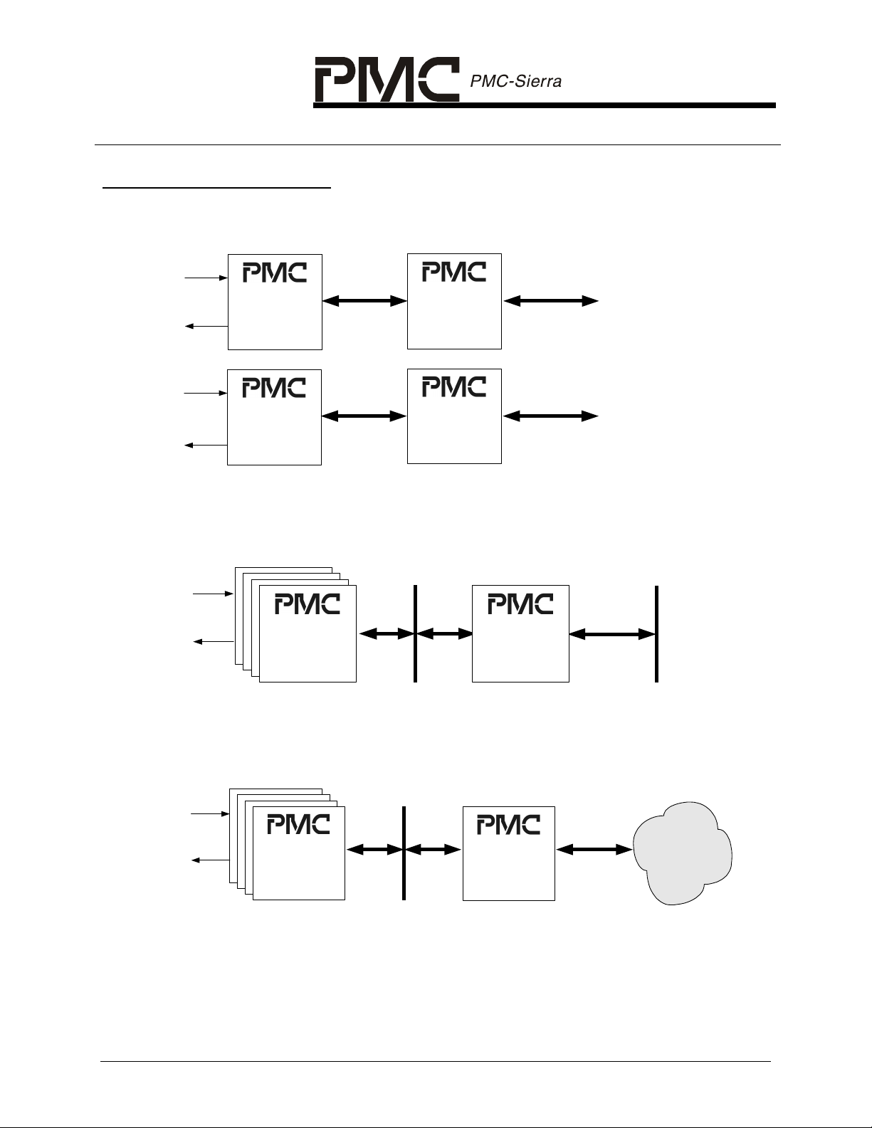
4 APPLICATION EXAMPLES
Figure 1 – T1/E1 Framer/Transceiver Application
8 x T1 lines
8 x E1 lines
OCTLIU
PM4318
OCTLIU
PM4318
Clock and Data
TOCTL
PM4388
Octal T1 Framer
Clock and Data
EOCTL
PM6388
Octal E1 Framer
Backplane
Backplane
Figure 2 – High Density T1/E1 Framer/Transceiver Application
SBI
32 T1/J1
or E1 lines
OCTLIU
OCTLIU
OCTLIU
OCTLIU
PM4318
PM4318
PM4318
PM4318
4xOCTLIU
TE32
PM4332
T1/J1/E1 Framer
H-MVIP or SBI
Figure 3 – High Density Leased Line Circuit Emulation Application
SBI
32 T1/J1
or E1 lines
PROPRIETARY AND CONFIDENTIAL TO PMC-SIERRA, INC., AND FOR ITS CUSTOMERS’ INTERNAL USE 7
OCTLIU
OCTLIU
OCTLIU
OCTLIU
PM4318
PM4318
PM4318
PM4318
4xOCTLIU
AAL1gator 32
PM73122
AAL1 SAR
Utopia L2
ATM
Backbone
Page 17
PRELIMINARY
DATASHEET
PMC- 2001578 ISSUE 3 OCTAL E1/T1/J1 LINE INTERFACE DEVICE
PM4318 OCTLIU
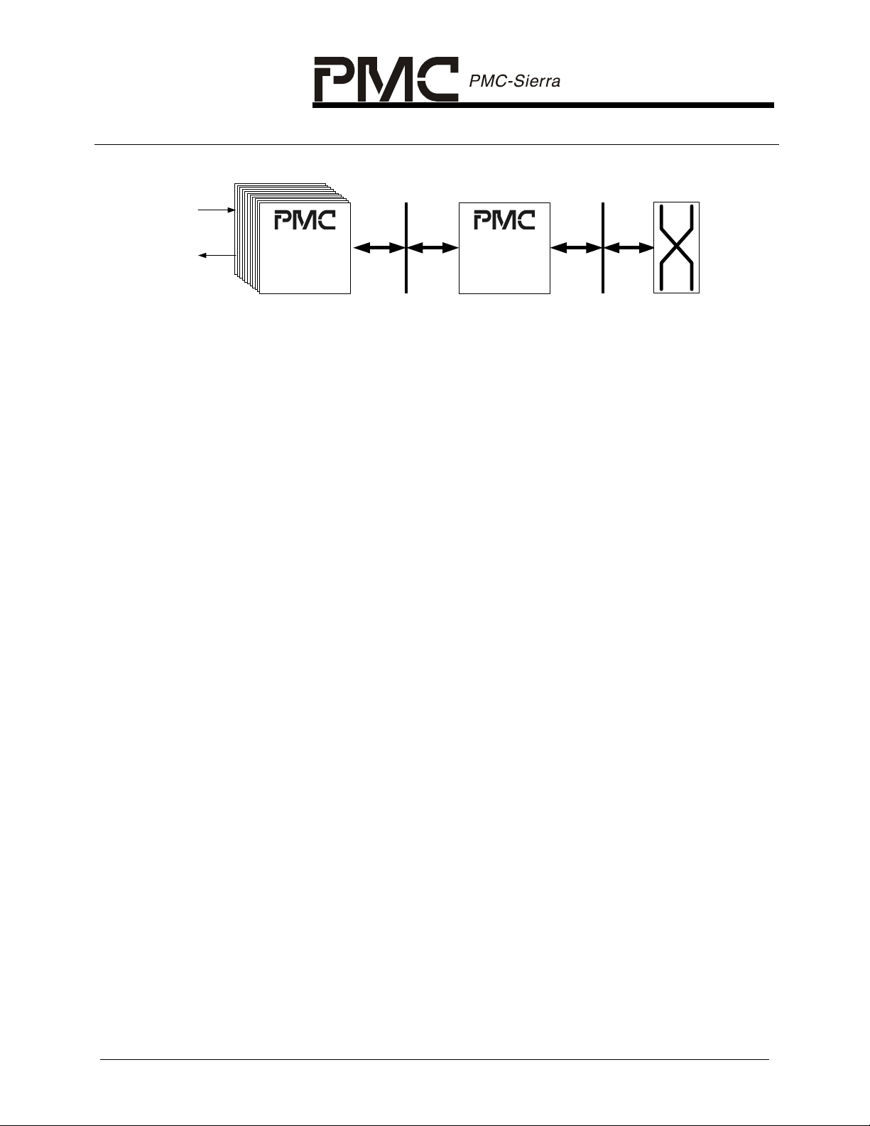
Figure 4 – Metro Optical Access Equipment
84 T1/J1
or 63 E1 lines
OCTLIU
OCTLIU
OCTLIU
OCTLIU
OCTLIU
OCTLIU
OCTLIU
OCTLIU
OCTLIU
OCTLIU
OCTLIU
PM4318
PM4318
PM4318
PM4318
PM4318
PM4318
PM4318
PM4318
PM4318
PM4318
PM4318
11xOCTLIU or
8xOCTLIU
SBI
TEMAP-84
PM5366
T1/E1 VT/TU Mapper
Telecom Bus
Cross Connect
PROPRIETARY AND CONFIDENTIAL TO PMC-SIERRA, INC., AND FOR ITS CUSTOMERS’ INTERNAL USE 8
Page 18
PRELIMINARY
PM4318 OCTLIU
DATASHEET
PMC- 2001578 ISSUE 3 OCTAL E1/T1/J1 LINE INTERFACE DEVICE
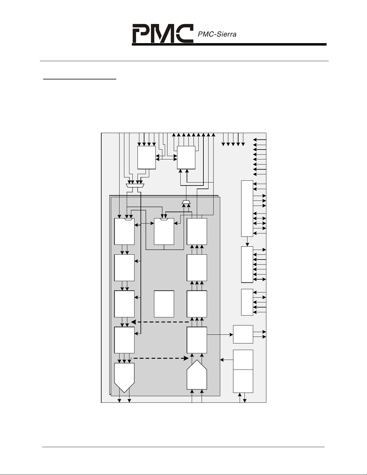
5 BLOCK DIAGRAM
Figure 5 – OCTLIU Block Diagram – LIUs Enabled
REFCLK
AC1FP
TDN[8:1]
TDP[8:1]
TCLK[8:1]
ADATA[7:0]
ADP
EXSBI-8
XIBC
Generator
back Code
Inband Loop-
XPDE
Enforcer
Pulse Density
APL
SBI Extract
AV5
DC1FP
DDATA[7:0]
DDP
DPL
C1FPOUT
PRBS
Pattern
Detector
Generator /
DV5
RDP[8:1]
RDN/RLCV[8:1]
RCLK[8:1]
DACTIVE
INSBI-8
SBI Insert
RJAT
Attenuator
Digital Jitter
-
IBCD
Detector
back Code
Inband Loop
VCLK
FBLOW
RSTB
SBI_EN
SBI2CLK
LEN1[2:0]
LEN2[2:0]
LEN3[2:0]
LEN4[2:0]
LEN5[2:0]
LEN6[2:0]
LEN7[2:0]
LEN8[2:0]
HW_ONLY
SRCODE
SRCEN
SRCCLK
SRCDO
H/W only
LIU Octant x 8
Auto-config
SRCASC
SREN
SRCLK
SRDI
SRDO
INTB
RDB
WRB
CSB
ALE
A[10:0]
D[7:0]
TRSTB
TDO
PMON
LCODE
Encoder
HDB3 Line
AMI / B8ZS /
TJAT
Attenuator
Digital Jitter
(Diagnostic
Digit al
XLPG
Transmit LIU
TXTIP1[8:1]
TXTIP2[8:1]
TXRING1[8:1]
TXRING2[8:1]
Monitor
Performance
Loopback)
PDVD
Viol. Detector
Pulse Density
(Line
Loopback)
CDRC
Clk/Data
Recovery
RLPS
Receive LIU
RXTIP[8:1]
RXRING[8:1]
JTAG uP Interface
LOS
Serial
Output
TOPS
Timi ng
Options
CSD
Clock
Synthesis /
Distribution
XCLK
RSYNC
TDI
TMS
TCK
LOS
LOS_L1
PROPRIETARY AND CONFIDENTIAL TO PMC-SIERRA, INC., AND FOR ITS CUSTOMERS’ INTERNAL USE 9
Page 19
PRELIMINARY
PM4318 OCTLIU
DATASHEET
PMC- 2001578 ISSUE 3 OCTAL E1/T1/J1 LINE INTERFACE DEVICE
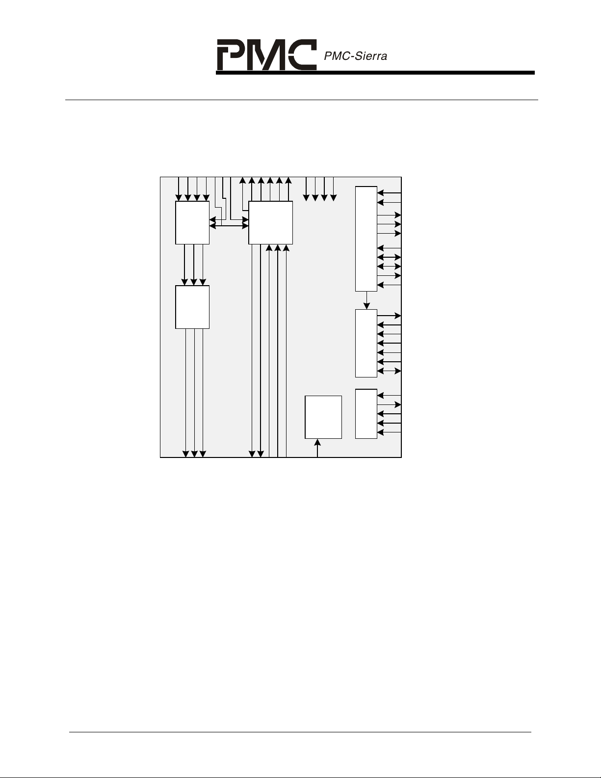
Figure 6 – OCTLIU Block Diagram – SBI to Clk/Data Converter, LIUs Disabled
REFCLK
AC1FP
Store x8EDATA[8:1]
AV5
DC1FP
DDATA[7:0]
DDP
DPL
C1FPOUT
DV5
DACTIVE
INSBI-8
SBI Insert
SBI2CLK
VCLK
RSTB
SBI_EN
HW _ONLY
SRCODE
SRCEN
SRCCLK
SRCDO
H/W only
Auto-config
SRCASC
SREN
SRCLK
SRDI
SRDO
INTB
RDB
WRB
CSB
ALE
A[10:0]
D[7:0]
ADATA[7:0]
ADP
APL
EXSBI-8
SBI Extract
ELST
Elastic
TRSTB
TDO
CSD
Clock
Synthesis /
Distribution
EFP
ECLK
IFP_IN
ICLK_IN
IFP_OUT
ICLK_OUT
IDATA[8:1]
XCLK
JTAG uP Interface
TDI
TMS
TCK
PROPRIETARY AND CONFIDENTIAL TO PMC-SIERRA, INC., AND FOR ITS CUSTOMERS’ INTERNAL USE 10
Page 20

PRELIMINARY
DATASHEET
PMC- 2001578 ISSUE 3 OCTAL E1/T1/J1 LINE INTERFACE DEVICE
PM4318 OCTLIU
6 DESCRIPTION
The PM4318 Octal E1/T1/J1 Line Interface Device (OCTLIU) is a monolithic integrated circuit
suitable for use in long haul and short haul T1, J1 and E1 systems with a minimum of external
circuitry. The OCTLIU is configurable via microprocessor control or SPI-compatible serial PROM
interface, allowing feature selection without changes to external wiring.
Analogue circuitry is provided to allow direct reception of long haul E1 and T1 compatible signals
with up to 36 dB cable loss (at 1.024 MHz) in E1 mode or up to 36 dB cable loss (at 772 kHz) in
T1 mode using a minimum of external components. Typically, only line protection, a transformer
and a line termination resistor are required.
The OCTLIU recovers clock and data from the line. Decoding of AMI, HDB3 and B8ZS line codes
is supported. In T1 mode, the OCTLIU also detects the presence of in-band loop back codes.
The OCTLIU supports detection of loss of signal, pulse density violation and line code violation
alarm conditions. Line code violations are accumulated for performance monitoring purposes.
Internal analogue circuitry allows direct transmission of long haul and short haul T1 and E1
compatible signals using a minimum of external components. Typically, only line protection, a
transformer and an optional line termination resistor are required. Digitally programmable pulse
shaping allows transmission of DSX-1 compatible signals up to 655 feet from the cross-connect,
E1 short haul pulses into 120 ohm twisted pair or 75 ohm coaxial cable, E1 long haul pulses into
120 ohm twisted pair as well as long haul DS-1 pulses into 100 ohm twisted pair with integrated
support for LBO filtering as required by the FCC rules. In addition, the programmable pulse
shape extending over 5-bit periods allows customization of short haul and long haul line interface
circuits to application requirements.
Each channel of the OCTLIU can generate a low jitter transmit clock from the input clock source
and also provide jitter attenuation in the receive path. A low jitter recovered T1 clock can be
routed outside the OCTLIU for network timing applications.
Serial PCM interfaces to each T1/E1 LIU allow 1.544 Mbit/s or 2.048 Mbit/s backplane
receive/backplane transmit system interfaces to be directly supported. Data may be transferred
either as dual rail line pulses or single rail DS-1/E1 data. Alternatively, the OCTLIU supports an
8-bit parallel SBI interface for interfacing to high-density framers.
The OCTLIU may be configured to operate in a mode in which the LIUs are disabled and the
device acts as a converter between the SBI interface and serial clock and data. Up to 8 serial
data streams (sharing a common clock and frame pulse) may be mapped on to the SBI bus in
this mode.
The OCTLIU may be configured, controlled and monitored via a generic 8-bit microprocessor bus
through which all internal registers are accessed. Alternatively, the device may be operated in a
‘hardware only’ mode in which no microprocessor is required. In this case, the OCTLIU reads
configuration information from an SPI-compatible serial PROM interface on power up. Multiple
OCTLIUs can be configured from a single serial PROM via a cascade interface on the OCTLIU.
PROPRIETARY AND CONFIDENTIAL TO PMC-SIERRA, INC., AND FOR ITS CUSTOMERS’ INTERNAL USE 11
Page 21

PRELIMINARY
PM4318 OCTLIU
DATASHEET
PMC- 2001578 ISSUE 3 OCTAL E1/T1/J1 LINE INTERFACE DEVICE
7 PIN DIAGRAM
The OCTLIU is packaged in a 288-pin Tape-SBGA package having a body size of 23mm by
23mm.
Figure 7 – Pin Diagram
22212019181716151413121110987654321
ALE/
A
LEN4[2]
B VDD3V3 VDD3V3
A[8]/
C
LEN3[2]
A[4]/
D
LEN2[1]
A[0]/
E
LEN1[0]
F RAVS1[1] RAVD2[1] QAVD[1]
G RAVD1[1] RXTIP[1] RAVS2[1] VDD3V3 RAVS2[8] RXTIP[8] RAVS1[7] TXRING1 [7] G
VSS
A[9]/
LEN4[0]
A[5]/
LEN2[2]
A[1]/
LEN1[1]
D[1]/
LEN6[2]
CSB/
LEN5[2]
A[10]/
LEN4[1]
A[6]/
LEN3[0]
A[2]/
LEN1[2]
D[2]/
LEN7[0]
LEN7[2]
D[0]/
LEN6[1]
LEN7[1]
RDB/
VDD3V3 VDD3V3 VSS
LEN5[1]
WRB/
VSS
LEN5[0]
A[7]/
LEN3[1]
A[3]/
LEN2[0]
D[4]/
VSS VDD1V8 TAVS2[1] TXRING2 [1] TXRING1 [1] TXTIP1[1] TXTIP2[1] TXTIP2 [8] TXTIP1 [8] TXRING1 [8] TXRING2 [8] RS TB LOS SRCCLK SRCLK VDD3V3 TDI A
D[3]/
D[6]/
SBI_EN QAVS[4] RES[5] TAVD3[1] TAVS3[8] TAVD2[8] QAVD[4] VDD1V8 VDD3V3 RES[1] RES[6] SRCDO SRDO SRCASC TDO HW_ONLY B
LEN8[1]
D[7]/
CAVD TAVD2[1] TAVS3[1] TAVD3[8] TAVS2[8] VSS VSS LOS_L1 SRCODE SRCEN SREN VSS TCK SBI2CLK C
LEN8[2]
INTB/
LEN6[0]
D[5]/
VSS
CAVS TAVS1[1] TAVD1[1] TAVD1[8] TAVS1[8] XCLK
LEN8[0]
RSYNC/
VDD3V3 SRDI VSS NC TMS VDD3V3 RAVS1[ 8] D
ICLK_OUT
TRSTB VSS RAVD2[8] RAVD2[7 ] E
QAVS[3] RES[4] RAVS2[7] TXRING2 [7] F
H TXRING2 [2] RAVD2[2] RAVS2[2] RXRING[1] RXRING [8] RAVD1[8] RAVD1[7] TXTIP1 [7] H
J TXRING1 [2] RXTIP[2] RAVS1[2] RXRING [2] RXRING [7] RXTIP[7] TAVS2[7] TXTIP2 [7] J
K TXTIP1[2] RAVD1[2] TAVS2[2] TAVS1[2] TAVS1[7] TAVD2[7] TAVD3[7] TXTIP2 [6] K
L TXT IP2 [2] TAVD2[2] TAVD3[2] TAV D1[2]
M TXTIP2 [3] TAVS3[2] TAVS3[3] TAVD1[3] TAVD1[6] TAVD3[6] TAVD2[6] TXRING1 [6] M
N TXTIP1 [3] TAVD3[3] TAVD2[3] TAVS1[3] TAVS1[6] TAVS2[6] RAVD1[6] TXRING2 [6] N
P TXRING1 [3] TAVS2[3] RAVD1[3] RXRING [3] RXRING [6] RAVS1[6] RAVD2[6] RXTIP[6] P
R TXRING2 [3] RXTIP[3] RAVD2[3] RXTIP[4] RXTIP[5] RXRING [5] RAVD1[5] RAVS2[6] R
T RAVS1[3] RAVS2[3] RAVD1[4] RAVS2[4] QAVD[3] RAVS2[5] RAVD2[5] RAVS1[5] T
U RXRING [4] RAVS1[4] RAVD2[4]
V RES[1] QAVS[1] VSS
TDP[1]/
W
Y
AA
AB VSS VSS VSS
TDN[1]/
ADATA[0]
REFCLK
TDN[2]/
TDP[3]/
AC1FP
ADATA[2]
TCLK[3]/
TDN[3]/
IDATA[3]
DC1FP
22212019181716151413121110987654321
TCLK[1]/
IDATA[1]
TDP[2]/
ADATA[1]
TCLK[2]/
VDD3V3 TDN[4]/ ADP VDD3V3 VDD3V3
IDATA[2]
TDP[4]/
VDD3V3
TCLK[4]/
IDATA[4]
ADATA[3]
RCLK[1]/
EDATA[1]
RDP[1]/
DDATA[0]
VSS
RCLK[2]/
EDATA[2]
RDN[1]/
RLCV[1]/
IFP_OUT
RDP[2]/
DDATA[1]
VSS VSS
RDN[2]/
RLCV[2]/
EFP
RCLK[3 ]/
EDATA[3]
RDP[3]/
DDATA[2]
RDN[3]/
RLCV[3]/
C1FPOUT
VDD3V3
RCLK[4]/
EDATA[4]
RDP[4]/
DDATA[3]
Bottom View
RDP[5]/
VSS TAVS1[4] TAVD1[4] TAVD1[5] TAVS1[5] VDD1V8
RDN[4]/
RLCV[4]/
TAVS2[4] TAVD3[4] TAVS3[5] TAVD2[5] RES[3]
DDP
VDD1V8 QAVD[2] TAVD2[4] TAVS3[4] TAVD3[5] TAVS2[5] QAVS[2] VSS VSS
TXRING2 [4] TXRING1 [4] TXTIP1[4] TXTIP2 [4] TXTIP2 [5] TXTIP1[5] TXRING1 [5] TXRING2 [5]
DDATA[4]
RDN[5]/
RLCV[5 ]/
DPL
RCLK[6 ]/
EDATA[6]
VDD3V3 VSS
RCLK[7 ]/
EDATA[7]
RCLK[5 ]/
EDATA[5]
TAVD1[7] TAVS3[7] TAVS3[6] TXTIP1[6] L
TCLK[7]/
TDN[8]/
IDATA[7]
IFP_IN
TCLK[6]/
TDN[6]/ AV5
IDATA[6]
RDP[8]/
NC VDD3V3
DDATA[7]
RDN[8]/
RDP[7]/
RLCV[8]/
DDATA[6]
RDP[6]/
DDATA[5]
RDN[6]/
RLCV[6 ]/
DV5
VSS
DACTIVE
RDN[7]/
RLCV[7]/
VDD3V3 VSS TDN[5]/ APL AA
ECLK
VDD3V3 VSS
TDP[8]/
ADATA[7]
TDN[7]/
ICLK_IN
TCLK[5]/
IDATA[5]
TDP[5]/
ADATA[4]
RCLK[8]/
EDATA[8]
VSS U
TCLK[8]/
IDATA[8]
TDP[7]/
ADATA[6]
TDP[6]/
ADATA[5]
VDD3V3 AB
V
W
Y
PROPRIETARY AND CONFIDENTIAL TO PMC-SIERRA, INC., AND FOR ITS CUSTOMERS’ INTERNAL USE 12
Page 22

PRELIMINARY
DATASHEET
PMC- 2001578 ISSUE 3 OCTAL E1/T1/J1 LINE INTERFACE DEVICE
PM4318 OCTLIU
8 PIN DESCRIPTION
By convention, where a bus of eight pins indexed [8:1] is present, the index indicates to which
octant the pin applies. With TCLK[8:1], for example, TCLK[1] applies to octant #1, TCLK[2]
applies to octant #2, etc.
Pin Name Type Pin
Function
No.
T1 and E1 System Side Serial Clock and Data Interface
TCLK[1]/IDATA[1]
TCLK[2]/IDATA[2]
TCLK[3]/IDATA[3]
TCLK[4]/IDATA[4]
TCLK[5]/IDATA[5]
TCLK[6]/IDATA[6]
TCLK[7]/IDATA[7]
TCLK[8]/IDATA[8]
TDP[1]/ADATA[0]
TDP[2]/ADATA[1]
TDP[3]/ADATA[2]
TDP[4]/ADATA[3]
TDP[5]/ADATA[4]
TDP[6]/ADATA[5]
TDP[7]/ADATA[6]
TDP[8]/ADATA[7]
Input U19
W20
AA22
AA20
W2
V3
U4
V1
Input W22
V19
Y21
Y19
Y2
Y1
W1
U2
The Transmit Clock inputs (TCLK[8:1]) should be 1.544 MHz for
DS1 or 2.048 MHz for E1 data streams and are used to sample
the corresponding TDP[8:1] and TDN[8:1] signals.
TCLK[8:1] share the same pins as the IDATA[8:1] inputs.
TCLK[8:1] are selected when SBI2CLK is tied low.
Transmit Positive Data (TDP[8:1]). When in single-rail mode,
these inputs are the NRZ data signals to be transmitted. These
inputs can be configured to be active high or active low. When in
dual-rail mode, these inputs are the NRZ positive data signals to
be transmitted.
TDP[8:1] can be sampled on either the rising or falling edges of
the corresponding TCLK[8:1].
TDP[8:1] share the same pins as the ADATA[7:0] inputs.
TDP[8:1] are selected when SBI_EN and SBI2CLK are both tied
low.
TDN[1]/REFCLK
TDN[2]/AC1FP
TDN[3]/DC1FP
TDN[4]/ADP
TDN[5]/APL
TDN[6]/AV5
TDN[7]/ICLK_IN
TDN[8]/IFP_IN
PROPRIETARY AND CONFIDENTIAL TO PMC-SIERRA, INC., AND FOR ITS CUSTOMERS’ INTERNAL USE 13
Input W21
Y22
AA21
W18
AA1
V4
V2
U3
Transmit Negative Data (TDN[8:1]). When in dual-rail mode,
these inputs are the NRZ negative data signals to be transmitted.
These inputs can be sampled on either the rising or falling edges
of the corresponding TCLK[8:1]. These input pins are ignored if
the device is configured for single-rail (unipolar) transmit mode.
TDN[8:1] share the same pins as the REFCLK, AC1FP, DC1FP,
ADP, APL, AV5, ICLK_IN and IFP_IN inputs. TDN[8:1] are
selected when SBI_EN and SBI2CLK are both tied low.
Page 23

PRELIMINARY
DATASHEET
PMC- 2001578 ISSUE 3 OCTAL E1/T1/J1 LINE INTERFACE DEVICE
PM4318 OCTLIU
Pin Name Type Pin
No.
RCLK[1]/EDATA[1]
RCLK[2]/EDATA[2]
RCLK[3]/EDATA[3]
RCLK[4]/EDATA[4]
RCLK[5]/EDATA[5]
RCLK[6]/EDATA[6]
RCLK[7]/EDATA[7]
RCLK[8]/EDATA[8]
RDP[1]/DDATA[0]
RDP[2]/DDATA[1]
RDP[3]/DDATA[2]
RDP[4]/DDATA[3]
RDP[5]/DDATA[4]
RDP[6]/DDATA[5]
RDP[7]/DDATA[6]
RDP[8]/DDATA[7]
Output AA19
AA18
Y16
AA15
AB6
W7
W6
AB2
Output AB19
Y17
AB16
AB15
W8
AA5
Y5
W5
Function
Recovered Clock Output (RCLK[8:1]). RCLK[8:1] is the clock
recovered from the RXTIP[8:1] and RXRING[8:1] input signals.
RCLK[8:1] share the same pins as the EDATA[8:1] outputs.
RCLK[8:1] are selected when SBI2CLK is tied low.
Receive Digital Positive Data (RDP[8:1]). When in single rail
mode, RDP[8:1] output NRZ sampled DS-1 or E1 data which has
been decoded by AMI, B8ZS, or HDB3 line code rules. When in
dual rail mode, RDP[8:1] output NRZ sampled bipolar positive
pulses.
RDP[8:1] can be updated on either the falling or rising RCLK[8:1]
edge.
RDP[8:1] share the same pins as the DDATA[7:0] outputs.
RDP[8:1] are selected when SBI_EN and SBI2CLK are both tied
low.
RDN/RLCV[1]/IFP_OUT
RDN/RLCV[2]/EFP
RDN/RLCV[3]/C1FPOUT
RDN/RLCV[4]/DDP
RDN/RLCV[5]/DPL
RDN/RLCV[6]/DV5
RDN/RLCV[7]/ECLK
RDN/RLCV[8]/DACTIVE
Output AB18
AB17
W15
Y14
Y8
AB5
AA4
Y4
Receive Digital Negative Data/Line Code Violation Indication
(RDN/RLCV[8:1]). When in dual rail mode, RDN/RLCV[8:1]
output NRZ sampled bipolar negative pulses. When in single rail
mode, RDN/RLCV[8:1] output a NRZ pulse whenever a line code
violation or excess zeros condition is detected.
RDN/RLCV[8:1] can be updated on either the falling or rising
RCLK[8:1] edge.
RDN/RLCV[8:1] share the same pins as the IFP_OUT, EFP,
C1FPOUT, DDP, DPL, DV5, ECLK and DACTIVE outputs.
RDN/RLCV[8:1] are selected when SBI_EN and SBI2CLK are
both tied low.
SBI System Side Interface
REFCLK/TDN[1] Input W21 The SBI reference clock signal (REFCLK) provides reference
timing for the SBI ADD and DROP busses.
REFCLK is nominally a 50% duty cycle clock of frequency 19.44
MHz ±50ppm.
REFCLK shares the same pin as the TDN[1] input. REFCLK is
selected when SBI_EN or SBI2CLK is tied high.
PROPRIETARY AND CONFIDENTIAL TO PMC-SIERRA, INC., AND FOR ITS CUSTOMERS’ INTERNAL USE 14
Page 24

PRELIMINARY
DATASHEET
PMC- 2001578 ISSUE 3 OCTAL E1/T1/J1 LINE INTERFACE DEVICE
PM4318 OCTLIU
Pin Name Type Pin
Function
No.
AC1FP/TDN[2] Input Y22 The SBI ADD bus C1 octet frame pulse signal (AC1FP) provides
frame synchronisation for devices connected via an SBI interface.
AC1FP must be asserted for 1 REFCLK cycle every 500 µs or
multiples thereof (i.e. every 9720 n REFCLK cycles, where n is a
positive integer). All devices connected to the SBI ADD bus must
be synchronised to a AC1FP signal from a single source.
AC1FP is sampled on the rising edge of REFCLK.
AC1FP shares the same pin as the TDN[2] input. AC1FP is
selected when SBI_EN or SBI2CLK is tied high.
DC1FP/TDN[3] Input AA21 The SBI DROP bus C1 octet frame pulse signal (DC1FP)
provides frame synchronisation for devices connected via an SBI
interface. DC1FP must be asserted for 1 REFCLK cycle every
500 µs or multiples thereof (i.e. every 9720 n REFCLK cycles,
where n is a positive integer). All devices connected to the SBI
DROP bus must be synchronised to a DC1FP signal from a single
source.
DC1FP is sampled on the rising edge of REFCLK.
DC1FP shares the same pin as the TDN[3] input. DC1FP is
selected when SBI_EN or SBI2CLK is tied high.
C1FPOUT/RDN/RLCV[3]
ADATA[0]/TDP[1]
ADATA[1]/TDP[2]
ADATA[2]/TDP[3]
ADATA[3]/TDP[4]
ADATA[4]/TDP[5]
ADATA[5]/TDP[6]
ADATA[6]/TDP[7]
ADATA[7]/TDP[8]
Output W15 The C1 octet frame pulse output signal (C1FPOUT) may be used
to provide frame synchronisation for devices interconnected via
an SBI interface. C1FPOUT is asserted for 1 REFCLK cycle
every 500 µs (i.e. every 9720 REFCLK cycles). If C1FPOUT is
used for synchronisation, it must be connected to the A/DC1FP
inputs of all the devices connected to the SBI ADD or DROP bus.
C1FPOUT is updated on the rising edge of REFCLK.
C1FPOUT shares the same pin as the RDN/RLCV[3] output.
C1FPOUT is selected when SBI_EN or SBI2CLK is tied high.
Input W22
V19
Y21
Y19
Y2
Y1
W1
U2
The SBI ADD bus data signals (ADATA[7:0]) contain time division
multiplexed transmit data from up to 84 independently timed links.
Link data is transported as T1 or E1 tributaries within the SBI
TDM bus structure. The OCTLIU may be configured to extract
data from up to 8 tributaries within the structure.
ADATA[7:0] are sampled on the rising edge of REFCLK.
ADATA[7:0] share the same pins as the TDP[8:1] inputs.
ADATA[7:0] are selected when SBI_EN or SBI2CLK is tied high.
PROPRIETARY AND CONFIDENTIAL TO PMC-SIERRA, INC., AND FOR ITS CUSTOMERS’ INTERNAL USE 15
Page 25

PRELIMINARY
DATASHEET
PMC- 2001578 ISSUE 3 OCTAL E1/T1/J1 LINE INTERFACE DEVICE
PM4318 OCTLIU
Pin Name Type Pin
Function
No.
ADP/TDN[4] Input W18 The SBI ADD bus parity signal (ADP) carries the even or odd
parity for the ADD bus signals. The parity calculation
encompasses the ADATA[7:0], APL and AV5 signals.
Multiple devices can drive the SBI ADD bus at uniquely assigned
tributary column positions. This parity signal is intended to detect
accidental driver clashes in the column assignment.
ADP is sampled on the rising edge of REFCLK.
ADP shares the same pin as the TDN[4] input. ADP is selected
when SBI_EN or SBI2CLK is tied high.
APL/TDN[5] Input AA1 The SBI ADD bus payload signal (APL) indicates valid data within
the SBI TDM bus structure. This signal is asserted during all
octets making up a tributary. This signal may be asserted during
the V3 octet within a tributary to accommodate negative timing
adjustments between the tributary rate and the fixed TDM bus
structure. This signal may be deasserted during the octet
following the V3 octet within a tributary to accommodate positive
timing adjustments between the tributary rate and the fixed TDM
bus structure.
APL is sampled on the rising edge of REFCLK.
APL shares the same pin as the TDN[5] input. APL is selected
when SBI_EN or SBI2CLK is tied high.
AV5/TDN[6] Input V4 The SBI ADD bus payload indicator signal (AV5) locates the
position of the floating payloads for each tributary within the SBI
TDM bus structure. Timing differences between the port timing
and the TDM bus timing are indicated by adjustments of this
payload indicator relative to the fixed TDM bus structure. All
movements indicated by this signal must be accompanied by
appropriate adjustments in the APL signal.
AV5 is sampled on the rising edge of REFCLK.
AV5 shares the same pin as the TDN[6] input. AV5 is selected
when SBI_EN or SBI2CLK is tied high.
PROPRIETARY AND CONFIDENTIAL TO PMC-SIERRA, INC., AND FOR ITS CUSTOMERS’ INTERNAL USE 16
Page 26

PRELIMINARY
DATASHEET
PMC- 2001578 ISSUE 3 OCTAL E1/T1/J1 LINE INTERFACE DEVICE
PM4318 OCTLIU
Pin Name Type Pin
No.
DDATA[0]/RDP[1]
DDATA[1]/RDP[2]
DDATA[2]/RDP[3]
DDATA[3]/RDP[4]
DDATA[4]/RDP[5]
DDATA[5]/RDP[6]
DDATA[6]/RDP[7]
DDATA[7]/RDP[8]
DDP/RDN/RLCV[4] Tristate
Tristate
Output
AB19
Y17
AB16
AB15
W8
AA5
Y5
W5
Y14 The SBI DROP bus parity signal (DDP) carries the even or odd
Output
Function
The SBI DROP bus data signals (DDATA[7:0]) contain time
division multiplexed receive data from up to 84 independently
timed links. Link data is transported as T1 or E1 tributaries within
the SBI TDM bus structure. The OCTLIU may be configured to
insert data into up to 8 tributaries within the structure. Multiple
LIU devices can drive the SBI DROP bus at uniquely assigned
tributary column positions. DDATA[7:0] are tristated when the
OCTLIU is not outputting data on a particular tributary column.
DDATA[7:0] are updated on the rising edge of REFCLK.
DDATA[7:0] share the same pins as the RDP[8:1] outputs.
DDATA[7:0] are selected when SBI_EN or SBI2CLK is tied high.
parity for the DROP bus signals. The parity calculation
encompasses the DDATA[7:0], DPL and DV5 signals.
Multiple LIU devices can drive this signal at uniquely assigned
tributary column positions. DDP is tristated when the OCTLIU is
not outputting data on a particular tributary column. This parity
signal is intended to detect accidental source clashes in the
column assignment.
DPL/RDN/RLCV[5] Tristate
Output
DDP is updated on the rising edge of REFCLK.
DDP shares the same pin as the RDN/RLCV[4] output. DDP is
selected when SBI_EN or SBI2CLK is tied high.
Y8 The SBI DROP bus payload signal (DPL) indicates valid data
within the SBI TDM bus structure. This signal is asserted during
all octets making up a tributary. This signal may be asserted
during the V3 octet within a tributary to accommodate negative
timing adjustments between the tributary rate and the fixed TDM
bus structure. This signal may be deasserted during the octet
following the V3 octet within a tributary to accommodate positive
timing adjustments between the tributary rate and the fixed TDM
bus structure.
Multiple LIU devices can drive this signal at uniquely assigned
tributary column positions. DPL is tristated when the OCTLIU is
not outputting data on a particular tributary column.
DPL is updated on the rising edge of REFCLK.
DPL shares the same pin as the RDN/RLCV[5] output. DPL is
selected when SBI_EN or SBI2CLK is tied high.
PROPRIETARY AND CONFIDENTIAL TO PMC-SIERRA, INC., AND FOR ITS CUSTOMERS’ INTERNAL USE 17
Page 27

PRELIMINARY
DATASHEET
PMC- 2001578 ISSUE 3 OCTAL E1/T1/J1 LINE INTERFACE DEVICE
PM4318 OCTLIU
Pin Name Type Pin
No.
DV5/RDN/RLCV[6] Tristate
AB5 The SBI DROP bus payload indicator signal (DV5) locates the
output
DACTIVE/RDN/RLCV[8]
Output Y4 The SBI DROP bus active indicator signal (DACTIVE) is asserted
Function
position of the floating payloads for each tributary within the SBI
TDM bus structure. Timing differences between the port timing
and the TDM bus timing are indicated by adjustments of this
payload indicator relative to the fixed TDM bus structure.
Multiple LIU devices can drive this signal at uniquely assigned
tributary column positions. DV5 is tristated when the OCTLIU is
not outputting data on a particular tributary column.
DV5 is updated on the rising edge of REFCLK.
DV5 shares the same pin as the RDN/RLCV[6] output. DV5 is
selected when SBI_EN or SBI2CLK is tied high.
whenever the OCTLIU is driving the SBI DROP bus signals,
DDATA[7:0], DDP, DPL and DV5.
DACTIVE is updated on the rising edge of REFCLK.
DACTIVE shares the same pin as the RDN/RLCV[8] output.
DACTIVE is selected when SBI_EN or SBI2CLK is tied high.
Transmit Line Interface
TXTIP1[1]
TXTIP1[2]
TXTIP1[3]
TXTIP1[4]
TXTIP1[5]
TXTIP1[6]
TXTIP1[7]
TXTIP1[8]
TXTIP2[1]
TXTIP2[2]
TXTIP2[3]
TXTIP2[4]
TXTIP2[5]
TXTIP2[6]
TXTIP2[7]
TXTIP2[8]
Analogue
Output
A12
K22
N22
AB12
AB9
L1
H1
A9
A11
L22
M22
AB11
AB10
K1
J1
A10
Transmit Analogue Positive Pulse (TXTIP1[8:1] and TXTIP2[8:1]).
When the transmit analogue line interface is enabled, the
TXTIP1[x] and TXTIP2[x] analogue outputs drive the transmit line
pulse signal through an external matching transformer. Both
TXTIP1[x] and TXTIP2[x] are normally connected to the positive
lead of the transformer primary. Two outputs are provided for
better signal integrity and must be shorted together on the board.
After a reset, TXTIP1[x] and TXTIP2[x] are high impedance. The
HIGHZ bit of the octant’s XLPG Line Driver Configuration register
must be programmed to logic 0 to remove the high impedance
state.
PROPRIETARY AND CONFIDENTIAL TO PMC-SIERRA, INC., AND FOR ITS CUSTOMERS’ INTERNAL USE 18
Page 28

PRELIMINARY
DATASHEET
PMC- 2001578 ISSUE 3 OCTAL E1/T1/J1 LINE INTERFACE DEVICE
PM4318 OCTLIU
Pin Name Type Pin
No.
TXRING1[1]
TXRING1[2]
TXRING1[3]
TXRING1[4]
TXRING1[5]
TXRING1[6]
TXRING1[7]
TXRING1[8]
TXRING2[1]
TXRING2[2]
TXRING2[3]
TXRING2[4]
TXRING2[5]
TXRING2[6]
TXRING2[7]
TXRING2[8]
Analogue
Output
A13
J22
P22
AB13
AB8
M1
G1
A8
A14
H22
R22
AB14
AB7
N1
F1
A7
Receive Line Interface
RXTIP[1]
RXTIP[2]
RXTIP[3]
RXTIP[4]
RXTIP[5]
RXTIP[6]
RXTIP[7]
RXTIP[8]
Analogue
Input
G21
J21
R21
R19
R4
P1
J3
G3
Function
Transmit Analogue Negative Pulse (TXRING1[8:1] and
TXRING2[8:1]). When the transmit analogue line interface is
enabled, the TXRING1[x] and TXRING2[x] analogue outputs drive
the transmit line pulse signal through an external matching
transformer. Both TXRING1[x] and TXRING2[x] are normally
connected to the negative lead of the transformer primary. Two
outputs are provided for better signal integrity and must be
shorted together on the board.
After a reset, TXRING1[x] and TXRING2[x] are high impedance.
The HIGHZ bit of the octant’s XLPG Line Driver Configuration
register must be programmed to logic 0 to remove the high
impedance state.
Receive Analogue Positive Pulse (RXTIP[8:1]). When the
analogue receive line interface is enabled, RXTIP[x] samples the
received line pulse signal from an external isolation transformer.
RXTIP[x] is normally connected directly to the positive lead of the
receive transformer secondary.
RXRING[1]
RXRING[2]
RXRING[3]
RXRING[4]
RXRING[5]
RXRING[6]
RXRING[7]
RXRING[8]
PROPRIETARY AND CONFIDENTIAL TO PMC-SIERRA, INC., AND FOR ITS CUSTOMERS’ INTERNAL USE 19
Analogue
Input
H19
J19
P19
U22
R3
P4
J4
H4
Receive Analogue Negative Pulse (RXRING[8:1]). When the
analogue receive line interface is enabled, RXRING[x] samples
the received line pulse signal from an external isolation
transformer. RXRING[x] is normally connected directly to the
negative lead of the receive transformer secondary.
Page 29

PRELIMINARY
DATASHEET
PMC- 2001578 ISSUE 3 OCTAL E1/T1/J1 LINE INTERFACE DEVICE
PM4318 OCTLIU
Pin Name Type Pin
No.
SBI to Clk/Data Converter Interface
SBI_EN
Input B16C1The SBI interface enable signals (SBI_EN, SBI2CLK) select
SBI2CLK
IDATA[1]/TCLK[1]
IDATA[2]/TCLK[2]
IDATA[3]/TCLK[3]
IDATA[4]/TCLK[4]
IDATA[5]/TCLK[5]
IDATA[6]/TCLK[6]
IDATA[7]/TCLK[7]
IDATA[8]/TCLK[8]
Input U19
W20
AA22
AA20
W2
V3
U4
V1
Function
between the SBI and serial clock/data system side interfaces and
allow selection of an operating mode in which the LIUs are
disabled and the OCTLIU functions as a converter between the
SBI interface and serial clk/data. The signals select the device
operating mode as follows:
SBI_EN SBI2CLK Mode
0 0 LIUs enabled, clk/data selected on system
side.
1 0 LIUs enabled, SBI interface selected on
system side.
0 1 LIUs disabled, converter mode.
1 1 Unused
The Ingress Data inputs (IDATA[8:1]) carry eight serial 1.544
Mbps or 2.048 Mbps data streams to be mapped on to the SBI
interface when the device is operating as a SBI to clk/data
converter. The eight serial data streams are sampled on the
rising edge of ICLK_IN.
IDATA[8:1] share the same pins as the TCLK[8:1] inputs.
IDATA[8:1] are selected when SBI2CLK is tied high.
ICLK_IN/TDN[7] Input V2 The Ingress Input Clock (ICLK_IN) should be 1.544 MHz for DS1
or 2.048 MHz for E1 data streams and is used to sample the
IDATA[8:1] and IFP_IN signals.
ICLK_IN shares the same pin as the TDN[7] input. ICLK_IN is
selected when SBI_EN or SBI2CLK is tied high.
IFP_IN/TDN[8] Input U3 The Ingress Frame Pulse input (IFP_IN) should be set high
during the framing bits of DS1 streams or during the first bit of the
framing octet of E1 data streams. IFP_IN is sampled on the
rising edge of ICLK_IN.
IFP_IN shares the same pin as the TDN[8] input. IFP_IN is
selected when SBI_EN or SBI2CLK is tied high.
ICLK_OUT/RSYNC Output D8 The Ingress Output Clock (ICLK_OUT) is a nominal 1.544 MHz
(for DS1) or 2.048 MHz (for E1) clock and may be used as a
source for the ICLK_IN clock if desired.
ICLK_OUT shares the same pin as the RSYNC output.
ICLK_OUT is selected when SBI2CLK is tied high.
PROPRIETARY AND CONFIDENTIAL TO PMC-SIERRA, INC., AND FOR ITS CUSTOMERS’ INTERNAL USE 20
Page 30

PRELIMINARY
DATASHEET
PMC- 2001578 ISSUE 3 OCTAL E1/T1/J1 LINE INTERFACE DEVICE
PM4318 OCTLIU
Pin Name Type Pin
Function
No.
IFP_OUT/RDN/RLCV[1]
Output AB18 The Ingress Frame Pulse output (IFP_OUT) is pulsed high every
193 ICLK_OUT cycles for DS1 and every 256 ICLK_OUT cycles
for E1. It may be used as a framing reference and as a source
for IFP_IN if desired. IFP_OUT is updated on the falling edge of
ICLK_OUT.
IFP_OUT shares the same pin as the RDN/RLCV[1] output.
IFP_OUT is selected when SBI_EN or SBI2CLK is tied high.
EDATA[1]/RCLK[1]
EDATA[2]/RCLK[2]
EDATA[3]/RCLK[3]
EDATA[4]/RCLK[4]
EDATA[5]/RCLK[5]
EDATA[6]/RCLK[6]
EDATA[7]/RCLK[7]
EDATA[8]/RCLK[8]
Output AA19
AA18
Y16
AA15
AB6
W7
W6
AB2
The Egress Data outputs (EDATA[8:1]) carry eight serial 1.544
Mbps or 2.048 Mbps data streams de-mapped from the SBI
interface when the device is operating as a SBI to clk/data
converter. The eight serial data streams are updated on the
falling edge of ECLK.
EDATA[8:1] share the same pins as the RCLK[8:1] outputs.
EDATA[8:1] are selected when SBI2CLK is tied high.
ECLK/RDN/RLCV[7] Output AA4 The Egress Clock output (ECLK) is a 1.544 MHz (for DS1) or
2.048 MHz (for E1) clock, recovered from one of the SBI
tributaries. The SBI tributary used to recover timing is selectable.
ECLK shares the same pin as the RDN/RLCV[7] output. ECLK is
selected when SBI_EN or SBI2CLK is tied high.
EFP/RDN/RLCV[2] Output AB17 The Egress Frame Pulse output (EFP) is set high during the
framing bits of DS1 streams or during the first bit of the framing
octet of E1 data streams. EFP is updated on the falling edge of
ECLK.
EFP shares the same pin as the RDN/RLCV[2] output. EFP is
selected when SBI_EN or SBI2CLK is tied high.
PROPRIETARY AND CONFIDENTIAL TO PMC-SIERRA, INC., AND FOR ITS CUSTOMERS’ INTERNAL USE 21
Page 31

PRELIMINARY
DATASHEET
PMC- 2001578 ISSUE 3 OCTAL E1/T1/J1 LINE INTERFACE DEVICE
PM4318 OCTLIU
Pin Name Type Pin
Function
No.
Timing Options Control
XCLK Input D9 Crystal Clock Input (XCLK). This signal provides a stable, global
timing reference for the OCTLIU internal circuitry via an internal
clock synthesizer. XCLK is a nominally jitter free clock at
1.544 MHz in T1 mode and 2.048 MHz in E1 mode.
In T1 mode, a 2.048 MHz clock may be used as a reference.
When used in this way, however, the intrinsic jitter specifications
in AT&T TR62411 may not be met.
RSYNC/ICLK_OUT Output D8 Recovered Clock Synchronization Signal (RSYNC). This output
signal is the recovered, jitter attenuated, receiver line rate clock
(1.544 or 2.048 MHz) of one of the eight T1 or E1 channels or,
optionally, the recovered, jitter attenuated clock synchronously
divided by 193 (T1 mode) or 256 (E1 mode) to create a 8 kHz
timing reference signal. The default is to source RSYNC from
octant #1.
When the OCTLIU is in a loss of signal state, RSYNC is derived
from the XCLK input or, optionally, is held high.
RSYNC shares the same pin as the ICLK_OUT output. RSYNC is
selected when SBI2CLK is tied low.
Alarm Interface
LOS Output A5 Loss of Signal Alarm (LOS). This signal outputs the LOS status
of the 8 LIU octants in a serial format which repeats every 8
XCLK cycles. The presence of the LOS status for LIU #1 on this
output is indicated by the LOS_L1 output pulsing high. On the
following XCLK cycle, the LOS status for LIU #2 is output, then
LIU #3, and so on.
This signal is intended for use in Hardware Only mode. When the
microprocessor interface is enabled, the status of the LOS alarm
can also be determined by reading the LOSV bit in the CDRC
Interrupt Status register.
LOS is updated on the falling edge of XCLK.
LOS_L1 Output C7 Loss of Signal LIU #1 indicator (LOS_L1). This signal is pulsed
high for one XCLK cycle every 8 XCLK cycles and indicates that
the LOS status for LIU #1 is being output on LOS.
LOS_L1 is updated on the falling edge of XCLK.
PROPRIETARY AND CONFIDENTIAL TO PMC-SIERRA, INC., AND FOR ITS CUSTOMERS’ INTERNAL USE 22
Page 32

PRELIMINARY
DATASHEET
PMC- 2001578 ISSUE 3 OCTAL E1/T1/J1 LINE INTERFACE DEVICE
PM4318 OCTLIU
Pin Name Type Pin
Function
No.
Misc. Control Signals
RSTB Input A6 Active Low Reset (RSTB). This signal provides an asynchronous
OCTLIU reset. RSTB is a Schmidt triggered input with an internal
pull up resistor.
RES[1] Input B7 This pin must be tied low for normal operation.
RES[2]
RES[3]
RES[4]
RES[5]
Analogue
I/O
V22
Y9
F3
B14
These pins must be connected to an analogue ground for normal
operation.
RES[6] Input B6 This pin must be tied to ground for normal operation.
PROPRIETARY AND CONFIDENTIAL TO PMC-SIERRA, INC., AND FOR ITS CUSTOMERS’ INTERNAL USE 23
Page 33

PRELIMINARY
DATASHEET
PMC- 2001578 ISSUE 3 OCTAL E1/T1/J1 LINE INTERFACE DEVICE
PM4318 OCTLIU
Pin Name Type Pin
Function
No.
Microprocessor Interface
A[0]/LEN1[0]
A[1]/LEN1[1]
A[2]/LEN1[2]
A[3]/LEN2[0]
A[4]/LEN2[1]
A[5]/LEN2[2]
A[6]/LEN3[0]
A[7]/LEN3[1]
A[8]/LEN3[2]
A[9]/LEN4[0]
A[10]/LEN4[1]
Input E22
E21
E20
F19
D22
D21
D20
E19
C22
C21
C20
Address Bus (A[10:0]). This bus selects specific registers during
OCTLIU register accesses.
Signal A[10] selects between normal mode and test mode register
access. A[10] has an internal pull down resistor.
A[10:0] share the same pins as some of the LENx[2:0] inputs.
A[10:0] are selected when HW_ONLY is tied low.
ALE/LEN4[2] Input A22 Address Latch Enable (ALE). This signal is active high and
latches the address bus contents, A[10:0], when low. When ALE
is high, the internal address latches are transparent. ALE allows
the OCTLIU to interface to a multiplexed address/data bus. The
ALE input has an internal pull up resistor.
ALE shares the same pin as the LEN4[2] input. ALE is selected
when HW_ONLY is tied low.
WRB/LEN5[0] Input D18 Active Low Write Strobe (WRB). This signal is low during a
OCTLIU register write access. The D[7:0] bus contents are
clocked into the addressed register on the rising WRB edge while
CSB is low.
WRB shares the same pin as the LEN5[0] input. WRB is selected
when HW_ONLY is tied low.
RDB/LEN5[1] Input C19 Active Low Read Enable (RDB). This signal is low during
OCTLIU register read accesses. The OCTLIU drives the D[7:0]
bus with the contents of the addressed register while RDB and
CSB are low.
RDB shares the same pin as the LEN5[1] input. RDB is selected
when HW_ONLY is tied low.
CSB/LEN5[2] Input B20 Active Low Chip Select (CSB). CSB must be low to enable
OCTLIU register accesses. CSB must go high at least once after
power up to clear internal test modes. If CSB is not used, it
should be tied to an inverted version of RSTB, in which case,
RDB and WRB determine register accesses.
CSB shares the same pin as the LEN5[2] input. CSB is selected
when HW_ONLY is tied low.
PROPRIETARY AND CONFIDENTIAL TO PMC-SIERRA, INC., AND FOR ITS CUSTOMERS’ INTERNAL USE 24
Page 34

PRELIMINARY
DATASHEET
PMC- 2001578 ISSUE 3 OCTAL E1/T1/J1 LINE INTERFACE DEVICE
PM4318 OCTLIU
Pin Name Type Pin
Function
No.
INTB/LEN6[0] Open-
drain
Output
D17 Active low Open-Drain Interrupt (INTB). This signal goes low
when an unmasked interrupt event is detected on any of the
internal interrupt sources. Note that INTB will remain low until all
active, unmasked interrupt sources are acknowledged at their
source at which time, INTB will tristate.
INTB shares the same pin as the LEN6[0] input. INTB is selected
when HW_ONLY is tied low.
D[0]/LEN6[1]
D[1]/LEN6[2]
D[2]/LEN7[0]
D[3]/LEN7[1]
D[4]/LEN7[2]
D[5]/LEN8[0]
D[6]/LEN8[1]
D[7]/LEN8[2]
I/O B19
A20
A19
B18
A18
D15
B17
C15
Bidirectional Data Bus (D[7:0]). This bus provides OCTLIU
register read and write accesses.
D[7:0] share the same pins as some of the LENx[2:0] inputs.
D[7:0] are selected when HW_ONLY is tied low.
Hardware-Only Control Interface
HW_ONLY Input B1 The Hardware Only mode enable signal (HW_ONLY) selects
between the microprocessor-controlled and hardware-only modes
of operation. When HW_ONLY is tied low, the microprocessor
interface is enabled. When HW_ONLY is tied high, the hardwareonly control interface is enabled and the microprocessor interface
is unused.
SRCASC Input B3 Serial PROM Cascade Control (SRCASC). When SRCASC is
tied low, the OCTLIU acts as the Serial PROM master controller
and the SREN, SRCLK, SRDI and SRDO pins should be
connected to the serial PROM. When SRCASC is tied high, the
OCTLIU acts as a Serial PROM cascade slave and the SREN,
SRCLK and SRDO pins should be connected to the SRCEN,
SRCCLK and SRCDO pins of another OCTLIU device upstream
in the cascade.
SREN I/O C4 Serial PROM Enable (SREN). When operating as a Serial PROM
master (SRCASC tied low), the SREN pin functions as an output
and generates an active low chip select signal for the serial
PROM. When operating as a Serial PROM slave (SRCASC tied
high), the SREN pin functions as an input and indicates the
validity of cascade data on the SRDO input.
When configured as an output, SREN is updated on the falling
edge of SRCLK. When configured as an input, SREN is sampled
on the rising edge of SRCLK.
PROPRIETARY AND CONFIDENTIAL TO PMC-SIERRA, INC., AND FOR ITS CUSTOMERS’ INTERNAL USE 25
Page 35

PRELIMINARY
DATASHEET
PMC- 2001578 ISSUE 3 OCTAL E1/T1/J1 LINE INTERFACE DEVICE
PM4318 OCTLIU
Pin Name Type Pin
Function
No.
SRCLK I/O A3 Serial PROM Clock (SRCLK). When operating as a Serial PROM
master (SRCASC tied low), the SRCLK pin functions as an output
and generates a clock for the serial PROM. When operating as a
Serial PROM slave (SRCASC tied high), the SRCLK pin functions
as an input and is connected to the SRCCLK output of an
OCTLIU device upstream in the serial PROM cascade.
SRDI Output D6 Serial PROM Data In (SRDI). When operating as a Serial PROM
master (SRCASC tied low), the SRDI output is used to send read
commands to the serial PROM. When operating as a Serial
PROM slave (SRCASC tied high), SRDI is unused.
SRDI is updated on the falling edge of SRCLK.
SRDO Input B4 Serial PROM Data Out (SRDO). When operating as a Serial
PROM master (SRCASC tied low), the SRDO input receives data
from the serial PROM. When operating as a Serial PROM slave
(SRCASC tied high), the SRDO input receives data from the
SRCDO output of an OCTLIU device upstream in the serial
PROM cascade.
SRDO is sampled on the rising edge of SRCLK.
SRCEN Output C5 Serial PROM Cascade Enable (SRCEN). The SRCEN output is
asserted when valid data is being output on SRCDO.
SRCEN is updated on the falling edge of SRCCLK.
SRCCLK Output A4 Serial PROM Cascade Clock (SRCCLK). When operating as a
Serial PROM master (SRCASC tied low), the SRCCLK output is a
copy of the SRCLK output. When operating as a Serial PROM
slave (SRCASC tied high), the SRCCLK output is a copy of the
SRCLK input.
SRCDO Output B5 Serial PROM Cascade Data Out (SRCDO). The SRCDO output
is a buffered, retimed copy of the SRDO input.
SRCDO is updated on the falling edge of SRCCLK.
SRCODE Input C6 Serial PROM Code (SRCODE). The SRCODE input provides a
means for controlling the execution of configuration instructions
stored in the serial PROM. Instructions can be coded to execute
only if SRCODE is logic 0, only if SRCODE is logic 1 or
unconditionally. The SRCODE input thus allows the selection of
two different configuration sequences within a single PROM load.
This could be used, for example, to store two configurations for
T1 and E1 operation within one serial PROM.
PROPRIETARY AND CONFIDENTIAL TO PMC-SIERRA, INC., AND FOR ITS CUSTOMERS’ INTERNAL USE 26
Page 36

PRELIMINARY
DATASHEET
PMC- 2001578 ISSUE 3 OCTAL E1/T1/J1 LINE INTERFACE DEVICE
PM4318 OCTLIU
Pin Name Type Pin
No.
LEN1[0]/A[0]
LEN1[1]/A[1]
LEN1[2]/A[2]
LEN2[0]/A[3]
LEN2[1]/A[4]
LEN2[2]/A[5]
LEN3[0]/A[6]
LEN3[1]/A[7]
LEN3[2]/A[8]
LEN4[0]/A[9]
LEN4[1]/A[10]
LEN4[2]/ALE
LEN5[0]/WRB
LEN5[1]/RDB
LEN5[2]/CSB
LEN6[0]/INTB
LEN6[1]/D[0]
LEN6[2]/D[1]
Input E22
E21
E20
F19
D22
D21
D20
E19
C22
C21
C20
A22
D18
C19
B20
D17
B19
A20
Function
Line Length Build-out Select (LENn[2:0]). These signals can be
preset to select one of eight different pulse templates to be used
by the line transmitters, depending on line length, etc. LENn[2:0]
selects the pulse template for the line transmitter of octant #n.
LENn[2:0] share the same pins as the microprocessor interface
signals. LENn[2:0] are selected when HW_ONLY is tied high.
The LENn[2:0] inputs are latched following reset of the OCTLIU
and any changes to their value will have no effect on the
operation of OCTLIU until a subsequent reset.
LEN7[0]/D[2]
LEN7[1]/D[3]
LEN7[2]/D[4]
LEN8[0]/D[5]
LEN8[1]/D[6]
LEN8[2]/D[7]
A19
B18
A18
D15
B17
C15
PROPRIETARY AND CONFIDENTIAL TO PMC-SIERRA, INC., AND FOR ITS CUSTOMERS’ INTERNAL USE 27
Page 37

PRELIMINARY
DATASHEET
PMC- 2001578 ISSUE 3 OCTAL E1/T1/J1 LINE INTERFACE DEVICE
PM4318 OCTLIU
Pin Name Type Pin
Function
No.
JTAG Interface
TDO Tristate
Output
B2 Test Data Output (TDO). This signal carries test data out of the
OCTLIU via the IEEE 1149.1 test access port. TDO is updated
on the falling edge of TCK. TDO is a tri-state output that is tristated except when scanning of data is in progress.
TDI Input A1 Test Data Input (TDI). This signal carries test data into the
OCTLIU via the IEEE 1149.1 test access port. TDI is sampled on
the rising edge of TCK. TDI has an internal pull up resistor.
TCK Input C2 Test Clock (TCK). This signal provides timing for test operations
that can be carried out using the IEEE 1149.1 test access port.
TMS Input D3 Test Mode Select (TMS). This signal controls the test operations
that can be carried out using the IEEE 1149.1 test access port.
TMS is sampled on the rising edge of TCK. TMS has an internal
pull up resistor.
TRSTB Input E4 Active low Test Reset (TRSTB). This signal provides an
asynchronous OCTLIU test access port reset via the IEEE 1149.1
test access port. TRSTB is a Schmidt triggered input with an
internal pull up resistor. TRSTB must be asserted during the
power up sequence.
Analogue Power and Ground Pins
TAVD1[1]
TAVD1[2]
Analogue
Power
TAVD1[3]
TAVD1[4]
TAVD1[5]
TAVD1[6]
TAVD1[7]
TAVD1[8]
D12
L19
M19
W12
W11
M4
L4
D11
Note that if not used, TRSTB should be connected to the RSTB
input.
Transmit Analogue Power (TAVD1[8:1]). TAVD1[8:1] provide
power for the transmit LIU analogue circuitry. TAVD1[8:1] should
be connected to analogue +3.3 V.
PROPRIETARY AND CONFIDENTIAL TO PMC-SIERRA, INC., AND FOR ITS CUSTOMERS’ INTERNAL USE 28
Page 38

PRELIMINARY
DATASHEET
PMC- 2001578 ISSUE 3 OCTAL E1/T1/J1 LINE INTERFACE DEVICE
PM4318 OCTLIU
Pin Name Type Pin
No.
TAVD2[1]
TAVD2[2]
TAVD2[3]
TAVD2[4]
TAVD2[5]
TAVD2[6]
TAVD2[7]
TAVD2[8]
TAVD3[1]
TAVD3[2]
TAVD3[3]
TAVD3[4]
TAVD3[5]
TAVD3[6]
TAVD3[7]
TAVD3[8]
CAVD Analogue
Analogue
Power
C13
L21
N20
AA12
Y10
M2
K3
B11
B13
L20
N21
Y12
AA10
M3
K2
C11
C14 Clock Synthesis Unit Analogue Power (CAVD). CAVD supplies
Power
Function
Transmit Analogue Power (TAVD2[8:1], TAVD3[8:1]). TAVD2[8:1]
and TAVD3[8:1] supply power for the transmit LIU current DACs.
They should be connected to analogue +3.3 V.
power for the transmit clock synthesis unit. CAVD should be
connected to analogue +3.3 V.
TAVS1[1]
TAVS1[2]
TAVS1[3]
TAVS1[4]
TAVS1[5]
TAVS1[6]
TAVS1[7]
TAVS1[8]
Analogue
Ground
D13
K19
N19
W13
W10
N4
K4
D10
Transmit Analogue Ground (TAVS1[8:1]). TAVS1[8:1] provide
ground for the transmit LIU analogue circuitry. TAVS1[8:1] should
be connected to analogue GND.
PROPRIETARY AND CONFIDENTIAL TO PMC-SIERRA, INC., AND FOR ITS CUSTOMERS’ INTERNAL USE 29
Page 39

PRELIMINARY
DATASHEET
PMC- 2001578 ISSUE 3 OCTAL E1/T1/J1 LINE INTERFACE DEVICE
PM4318 OCTLIU
Pin Name Type Pin
No.
TAVS2[1]
TAVS2[2]
TAVS2[3]
TAVS2[4]
TAVS2[5]
TAVS2[6]
TAVS2[7]
TAVS2[8]
TAVS3[1]
TAVS3[2]
TAVS3[3]
TAVS3[4]
TAVS3[5]
TAVS3[6]
TAVS3[7]
TAVS3[8]
CAVS Analogue
Analogue
Ground
A15
K20
P21
Y13
AA9
N3
J2
C10
C12
M21
M20
AA11
Y11
L2
L3
B12
D14 Clock Synthesis Unit Analogue Ground (CAVS). CAVS supplies
Ground
Function
Transmit Analogue Ground (TAVS2[8:1], TAVS3[8:1]). TAVS2[8:1]
and TAVS3[8:1] supply ground for the transmit LIU current DACs.
They should be connected to analogue GND.
ground for the transmit clock synthesis unit. CAVS should be
connected to analogue GND.
RAVD1[1]
RAVD1[2]
RAVD1[3]
RAVD1[4]
RAVD1[5]
RAVD1[6]
RAVD1[7]
RAVD1[8]
RAVD2[1]
RAVD2[2]
RAVD2[3]
RAVD2[4]
RAVD2[5]
RAVD2[6]
RAVD2[7]
RAVD2[8]
Analogue
Power
Analogue
Power
G22
K21
P20
T20
R2
N2
H2
H3
F21
H21
R20
U20
T2
P2
E1
E2
Receive Analogue Power (RAVD1[8:1]). RAVD1[8:1] supplies
power for the receive LIU input equalizer. RAVD1[8:1] should be
connected to analogue +3.3 V.
Receive Analogue Power (RAVD2[8:1]). RAVD2[8:1] supplies
power for the receive LIU peak detect and slicer. RAVD2[8:1]
should be connected to analogue +3.3 V.
PROPRIETARY AND CONFIDENTIAL TO PMC-SIERRA, INC., AND FOR ITS CUSTOMERS’ INTERNAL USE 30
Page 40

PRELIMINARY
DATASHEET
PMC- 2001578 ISSUE 3 OCTAL E1/T1/J1 LINE INTERFACE DEVICE
PM4318 OCTLIU
Pin Name Type Pin
No.
RAVS1[1]
RAVS1[2]
RAVS1[3]
RAVS1[4]
RAVS1[5]
RAVS1[6]
RAVS1[7]
RAVS1[8]
RAVS2[1]
RAVS2[2]
RAVS2[3]
RAVS2[4]
RAVS2[5]
RAVS2[6]
RAVS2[7]
RAVS2[8]
QAVD[1]
QAVD[2]
QAVD[3]
QAVD[4]
Analogue
Ground
Analogue
Ground
Analogue
Power
F22
J20
T22
U21
T1
P3
G2
D1
G20
H20
T21
T19
T3
R1
F2
G4
F20
AA13
T4
B10
Function
Receive Analogue Ground (RAVS1[8:1]). RAVS1[8:1] supplies
ground for the receive LIU input equalizer. RAVS1[8:1] should be
connected to analogue GND.
Receive Analogue Ground (RAVS2[8:1]). RAVS2[8:1] supplies
ground for the receive LIU peak detect and slicer. RAVS2[8:1]
should be connected to analogue GND.
Quiet Analogue Power (QAVD[4:1]). QAVD[4:1] supplies power
for the core analogue circuitry. QAVD[4:1] should be connected
to analogue +3.3 V.
QAVS[1]
QAVS[2]
Analogue
Ground
QAVS[3]
QAVS[4]
Digital Power and Ground Pins
VDD1V8[1]
Power A16
VDD1V8[2]
VDD1V8[3]
VDD1V8[4]
V21
AA8
F4
B15
B9
W9
AA14
Quiet Analogue Ground (QAVS[4:1]). QAVS[4:1] supplies ground
for the core analogue circuitry. QAVS[4:1] should be connected
to analogue GND.
Core Power (VDD1V8[4:1]). The VDD1V8[4:1] pins should be
connected to a well decoupled +1.8V DC power supply.
PROPRIETARY AND CONFIDENTIAL TO PMC-SIERRA, INC., AND FOR ITS CUSTOMERS’ INTERNAL USE 31
Page 41

PRELIMINARY
DATASHEET
PMC- 2001578 ISSUE 3 OCTAL E1/T1/J1 LINE INTERFACE DEVICE
PM4318 OCTLIU
Pin Name Type Pin
No.
VDD3V3[1]
VDD3V3[2]
VDD3V3[3]
VDD3V3[4]
VDD3V3[5]
VDD3V3[6]
VDD3V3[7]
VDD3V3[8]
VDD3V3[9]
VDD3V3[10]
VDD3V3[11]
VDD3V3[12]
VDD3V3[13]
VDD3V3[14]
VDD3V3[15]
VDD3V3[16]
VDD3V3[17]
VDD3V3[18]
VDD3V3[19]
Power A2
B8
B21
B22
C17
C18
D2
D7
G19
W3
W16
W17
W19
Y7
Y15
Y20
AA3
AB1
AB4
Function
I/O Power (VDD3V3[19:1]). The VDD3V3[19:1] pins should be
connected to a well decoupled +3.3V DC power supply.
PROPRIETARY AND CONFIDENTIAL TO PMC-SIERRA, INC., AND FOR ITS CUSTOMERS’ INTERNAL USE 32
Page 42

PRELIMINARY
DATASHEET
PMC- 2001578 ISSUE 3 OCTAL E1/T1/J1 LINE INTERFACE DEVICE
PM4318 OCTLIU
Pin Name Type Pin
No.
VSS[1]
VSS[2]
VSS[3]
VSS[4]
VSS[5]
VSS[6]
VSS[7]
VSS[8]
VSS[9]
VSS[10]
VSS[11]
VSS[12]
VSS[13]
VSS[14]
VSS[15]
VSS[16]
VSS[17]
VSS[18]
VSS[19]
VSS[20]
VSS[21]
VSS[22]
VSS[23]
VSS[24]
VSS[25]
Ground A17
A21
C3
C8
C9
C16
D5
D16
D19
E3
U1
V20
W14
Y3
Y6
Y18
AA2
AA6
AA7
AA16
AA17
AB3
AB20
AB21
AB22
Function
Ground (VSS [25:1]). The VSS[25:1] pins should be connected to
Ground.
NC1
NC2
Open D4
W4
These pins must be left unconnected.
NOTES ON PIN DESCRIPTIONS:
1. All OCTLIU inputs and bi-directionals present minimum capacitive loading.
2. All OCTLIU inputs and bi-directionals, when configured as inputs, tolerate TTL logic levels.
3. All OCTLIU outputs and bi-directionals have at least 8 mA drive capability, except the LOS,
LOS_L1, TDO and serial PROM interface outputs, which have at least 6 mA drive capability.
The transmit analogue outputs (TXTIP and TXRING) have built-in short circuit current limiting.
4. Inputs RSTB, ALE, TMS, TDI and TRSTB have internal pull-up resistors.
5. Inputs A[10], RES[1], and RES[6] have internal pull-down resistors.
6. All unused inputs should be connected to GROUND.
PROPRIETARY AND CONFIDENTIAL TO PMC-SIERRA, INC., AND FOR ITS CUSTOMERS’ INTERNAL USE 33
Page 43

PRELIMINARY
DATASHEET
PMC- 2001578 ISSUE 3 OCTAL E1/T1/J1 LINE INTERFACE DEVICE
PM4318 OCTLIU
7. The 3.3 Volt power pins (i.e., TAVD1, TAVD2, TAVD3, CAVD, RAVD1, RAVD2, QAVD, and
VDD3V3) will be collectively referred to as V
DDall33
in this document.
8. Power to V
DDall33
should be applied before power to the VDD1V8 pins is applied. Similarly,
power to the VDD1V8 pins should be removed before power to V
9. The V
DDall33
voltage level should not be allowed to drop below the VDD1V8 voltage level
except when VDD1V8 is not powered.
DDall33
is removed.
PROPRIETARY AND CONFIDENTIAL TO PMC-SIERRA, INC., AND FOR ITS CUSTOMERS’ INTERNAL USE 34
Page 44

PRELIMINARY
PM4318 OCTLIU
DATASHEET
PMC- 2001578 ISSUE 3 OCTAL E1/T1/J1 LINE INTERFACE DEVICE
9 FUNCTIONAL DESCRIPTION
9.1 Octants
The OCTLIU’s eight E1/T1 line interface units operate independently and can be configured to
operate uniquely. The octants do share a common XCLK clock input and internal clock
synthesizer; hence only a single CSU Configuration register is present. Additionally, all octants
share a common E1/T1B mode register bit to select between T1 and E1 operation.
9.2 Receive Interface
The analogue receive interface is configurable to operate in both E1 and T1 short-haul and longhaul applications. Short-haul T1 is defined as transmission over less than 655 ft of cable. Shorthaul E1 is defined as transmission on any cable that attenuates the signal by less than 6 dB.
For long-haul signals, unequalized long- or short-haul bipolar alternate mark inversion (AMI)
signals are received as the differential voltage between the RXTIP and RXRING inputs. The
OCTLIU typically accepts unequalized signals that are attenuated for both T1 and E1 signals and
are non-linearly distorted by typical cables.
For short-haul, the slicing threshold is set to a fraction of the input signal’s peak amplitude, and
adapts to changes in this amplitude. The slicing threshold is programmable, but is typically 67%
and 50% for DSX-1 and E1 applications, respectively. Abnormally low input signals are detected
when the input level is below a programmable threshold, which is typically 140 mV for E1 and
105 mV for T1.
Figure 8 – External Analogue Interface Circuits
VDD
TXTIP
TXRING
ATB
RXTIP
RXRING
One of Eight
T1 or E1 LIUs
gnd
D1
1:n
inA
R1
inB
gnd
VDD
inA
R2
inB
gnd
outB
center tap
outA
T1
Phantom Feed
Circuit or Vsupply
as required
1:n
outB
center tap
outA
T2
L1
Z5
L2
Z6
F1
Z1
chassis gnd
Z2
F2
F3
Z3
Z4
F4
TTip
TRing
RTip
chassis gnd
RRing
PROPRIETARY AND CONFIDENTIAL TO PMC-SIERRA, INC., AND FOR ITS CUSTOMERS’ INTERNAL USE 35
Page 45

PRELIMINARY
DATASHEET
PMC- 2001578 ISSUE 3 OCTAL E1/T1/J1 LINE INTERFACE DEVICE
PM4318 OCTLIU
Figure 8 gives the recommended external protection circuitry for designs required to meet the
major surge immunity and electrical safety standards including FCC Part 68, UL1950, and
Bellcore TR-NWT-001089. This circuit has not been tested as of December, 1999. Please refer to
an upcoming PMC application note for more details.
For systems not requiring phantom feed or inter-building line protection, the Bi-directional
Transient Surge Suppressors (Z1-Z4), their associated ground connection and the center tap of
the transformer can be removed from the circuit.
See Table 1 for the descriptions of components for Figure 8.
Note that the crowbar devices (Z1 – Z4) are not required if the transformer’s isolation rating is not
exceeded.
Table 1 – External Component Descriptions
Component Description Part # Source
R1
R2
36.0Ω ±1%, 0.25W Resistor
27.0Ω ±1%, 0.25W Resistor
D1 Surge Protector Diode Array SRDA3.3-4 Semtech
T1 & T2
1:1.58 CT Transformers (E1 75Ω cable)
1:2 CT Transformers (otherwise)
Z1 – Z4 Bi-directional Transient Surge Suppressors P1800SC Teccor
Z5 – Z6 Bi-directional Transient Surge Suppressors P0720SC Teccor
L1 & L2 Dual Choke, 27µH PE-68624 Pulse
F1 – F4 Telecom/Time Lag Fuses F1250T Teccor
When operating in E1 mode with 75Ω cable, a 1:1.58 turns ratio transformer is specified in the
above table. It is in fact also possible to use a 1:2 turns ratio transformer, in which case the value
of R1 must be changed to 22.0Ω ±1% and the value of R2 must be changed to 18.0Ω ±1%.
9.3 Clock and Data Recovery (CDRC)
The Clock and Data Recovery function is provided by the Clock and Data Recovery (CDRC)
block. The CDRC provides clock and PCM data recovery, B8ZS and HDB3 decoding, line code
violation detection, and loss of signal detection. It recovers the clock from the incoming RZ data
pulses using a digital phase-locked-loop and reconstructs the NRZ data. Loss of signal is
indicated after a programmable threshold of consecutive bit periods of the absence of pulses on
both the positive and negative line pulse inputs and is cleared after the occurrence of a single line
pulse. An alternate loss of signal indication is provided which is cleared upon meeting an 1-in-8
pulse density criteria for T1 and a 1-in-4 pulse density criteria for E1. If enabled, a
microprocessor interrupt is generated when a loss of signal is detected and when the signal
returns. A line code violation is defined as a bipolar violation (BPV) for AMI-coded signals, is
Pulse
PROPRIETARY AND CONFIDENTIAL TO PMC-SIERRA, INC., AND FOR ITS CUSTOMERS’ INTERNAL USE 36
Page 46

PRELIMINARY
DATASHEET
PMC- 2001578 ISSUE 3 OCTAL E1/T1/J1 LINE INTERFACE DEVICE
PM4318 OCTLIU
defined as a BPV that is not part of a zero substitution code for B8ZS-coded signals, and is
defined as a bipolar violation of the same polarity as the last bipolar violation for HDB3-coded
signals.
In T1 mode, the input jitter tolerance of the OCTLIU complies with the Bellcore Document
TA-TSY-000170 and with the AT&T specification TR62411, as shown in Figure 9. The tolerance is
measured with a QRSS sequence (2
20
-1 with 14 zero restriction). The CDRC block provides two
algorithms for clock recovery that result in differing jitter tolerance characteristics. The first
algorithm (when the ALGSEL register bit is logic 0) provides good low frequency jitter tolerance,
but the high frequency tolerance is close to the TR62411 limit. The second algorithm (when
ALGSEL is logic 1) provides much better high frequency jitter tolerance at the expense of the low
frequency tolerance; the low frequency tolerance of the second algorithm is approximately 80%
that of the first algorithm.
Figure 9 – T1 Jitter Tolerance
Sine Wave
Jitter
Amplitude
P. to P. (UI)
Log Scale
10
1.0
0.3
0.2
0.1
0.1
Acceptable Range
0.310.30
Sine Wave Jitter Frequency (kHz) Log Scale
Bellcore Spec.
AT&T Spec.
100101.0
For E1 applications, the input jitter tolerance complies with the ITU-T Recommendation G.823
“The Control of Jitter and Wander Within Digital Networks Which are Based on the 2048 kbit/s
Hierarchy.” Figure 10 illustrates this specification and the performance of the phase-locked loop
when the ALGSEL register bit is logic 0.
PROPRIETARY AND CONFIDENTIAL TO PMC-SIERRA, INC., AND FOR ITS CUSTOMERS’ INTERNAL USE 37
Page 47

PRELIMINARY
DATASHEET
PMC- 2001578 ISSUE 3 OCTAL E1/T1/J1 LINE INTERFACE DEVICE
PM4318 OCTLIU
Figure 10 – Compliance with ITU-T Specification G.823 for E1 Input Jitter
DPLL TOLERANCE
10
SINEWAVE
JITTER
AMPLITUDE
P. TO P. (UI)
LOG SCALE
IN SPEC
REGION
1.5
1
REC. G823
JITTER
TOLERANCE
SPECIFICATION
0.2
WITH AMI ENCODED
15
2 -1 PRBS
DPLL TOLERANCE
WITH HDB3 ENCODED
15
2 -1 PRBS
0.1
34
10 10 10
2.4
SINEWAVE JITTER FREQUENCY, Hz - LOG SCALE
9.4 Receive Jitter Attenuator (RJAT)
The Receive Jitter Attenuator (RJAT) digital PLL attenuates the jitter present on the
RXTIP/RXRING inputs. The attenuation is only performed when the RJATBYP register bit is a
logic 0.
The jitter characteristics of the Receive Jitter Attenuator (RJAT) are the same as the Transmit
Jitter Attenuator (TJAT).
9.5 T1 Inband Loopback Code Detector (IBCD)
The T1 Inband Loopback Code Detection function is provided by the IBCD block. This block
detects the presence of either of two programmable INBAND LOOPBACK ACTIVATE and
DEACTIVATE code sequences in the receive data stream. Each INBAND LOOPBACK code
sequence is defined as the repetition of the programmed code in the PCM stream for at least 5.1
seconds. The code sequence detection and timing is compatible with the specifications defined
in T1.403-1993, TA-TSY-000312, and TR-TSY-000303. LOOPBACK ACTIVATE and
DEACTIVATE code indication is provided through internal register bits. An interrupt is generated
to indicate when either code status has changed.
1.8
5
PROPRIETARY AND CONFIDENTIAL TO PMC-SIERRA, INC., AND FOR ITS CUSTOMERS’ INTERNAL USE 38
Page 48

PRELIMINARY
DATASHEET
PMC- 2001578 ISSUE 3 OCTAL E1/T1/J1 LINE INTERFACE DEVICE
PM4318 OCTLIU
9.6 T1 Pulse Density Violation Detector (PDVD)
The Pulse Density Violation Detection function is provided by the PDVD block. The block detects
pulse density violations of the requirement that there be N ones in each and every time window of
8(N+1) data bits (where N can equal 1 through 23). The PDVD also detects periods of 16
consecutive zeros in the incoming data. Pulse density violation detection is provided through an
internal register bit. An interrupt is generated to signal a 16 consecutive zero event, and/or a
change of state on the pulse density violation indication.
9.7 Performance Monitor Counters (PMON)
The Performance Monitor block accumulates line code violation events with a saturating counter
over consecutive intervals as defined by the period between writes to trigger registers (typically 1
second). When the trigger is applied, the PMON transfers the counter value into holding registers
and resets the counter to begin accumulating events for the interval. The counter is reset in such
a manner that error events occurring during the reset are not missed. If the holding registers are
not read between successive triggers, an overrun register bit is asserted.
Triggering a counter transfer within an octant is performed by writing to any counter register
location within the octant or by writing to the “Line Interface Interrupt Source #1 / PMON Update”
register.
9.8 Pseudo Random Binary Sequence Generation and Detection (PRBS)
The Pseudo Random Binary Sequence Generator/Detector (PRBS) block is a software selectable
11
PRBS generator and checker for 2
-1, 215-1 or 220-1 PRBS polynomials for use in the T1 and E1
links. PRBS patterns may be generated and detected in either the transmit or receive directions.
The PRBS block can perform an auto synchronization to the expected PRBS pattern and
accumulates the total number of bit errors in two 24-bit counters. The error count accumulates
over the interval defined by successive writes to the Line Interface Interrupt Source #1 / PMON
Update register. When an accumulation is forced, the holding register is updated, and the
counter reset to begin accumulating for the next interval. The counter is reset in such a way that
no events are missed. The data is then available in the Error Count registers until the next
accumulation.
9.9 T1 Inband Loopback Code Generator (XIBC)
The T1 Inband Loopback Code Generator (XIBC) block generates a stream of inband loopback
codes (IBC) to be inserted into a T1 data stream. The IBC stream consists of continuous
repetitions of a specific code. The contents of the code and its length are programmable from 3 to
8 bits.
9.10 Pulse Density Enforcer (XPDE)
The Pulse Density Enforcer function is provided by the XPDE block. Pulse density enforcement
is enabled by a register bit within the XPDE.
PROPRIETARY AND CONFIDENTIAL TO PMC-SIERRA, INC., AND FOR ITS CUSTOMERS’ INTERNAL USE 39
Page 49

PRELIMINARY
DATASHEET
PMC- 2001578 ISSUE 3 OCTAL E1/T1/J1 LINE INTERFACE DEVICE
PM4318 OCTLIU
This block monitors the digital output of the transmitter and detects when the stream is about to
violate the ANSI T1.403 12.5% pulse density rule over a moving 192-bit window. If a density
violation is detected, the block can be enabled to insert a logic 1 into the digital stream to ensure
the resultant output no longer violates the pulse density requirement. When the XPDE is disabled
from inserting logic 1s, the digital stream from the transmitter is passed through unaltered.
9.11 Transmit Jitter Attenuator (TJAT)
The Transmit Jitter Attenuation function is provided by a digital phase lock loop and 80-bit deep
FIFO. The TJAT receives jittery, dual-rail data in NRZ format on two separate inputs, which
allows bipolar violations to pass through the block uncorrected. The incoming data streams are
stored in a FIFO timed to the transmit clock. The respective input data emerges from the FIFO
timed to the jitter attenuated clock.
The jitter attenuator generates the jitter-free 1.544 MHz or 2.048 MHz Transmit clock output by
adjusting the Transmit clock’s phase in 1/96 UI increments to minimize the phase difference
between the generated Transmit clock and input data clock to TJAT. Jitter fluctuations in the
phase of the input data clock are attenuated by the phase-locked loop within TJAT so that the
frequency of Transmit clock is equal to the average frequency of the input data clock. For T1
applications, to best fit the jitter attenuation transfer function recommended by TR 62411, phase
fluctuations with a jitter frequency above 5.7 Hz are attenuated by 6 dB per octave of jitter
frequency. Wandering phase fluctuations with frequencies below 5.7 Hz are tracked by the
generated Transmit clock. In E1 applications, the corner frequency is 7.6 Hz. To provide a
smooth flow of data out of TJAT, the Transmit clock is used to read data out of the FIFO.
If the FIFO read pointer (timed to the Transmit clock) comes within one bit of the write pointer
(timed to the input data clock), TJAT will track the jitter of the input clock. This permits the phase
jitter to pass through unattenuated, inhibiting the loss of data.
Jitter Characteristics
The TJAT Block provides excellent jitter tolerance and jitter attenuation while generating minimal
residual jitter. It can accommodate up to 61 Uipp of input jitter at jitter frequencies above 5.7 Hz
(7.6 Hz for E1). For jitter frequencies below 5.7 Hz (7.6 Hz for E1), more correctly called wander,
the tolerance increases 20 dB per decade. In most applications the TJAT Block will limit jitter
tolerance at lower jitter frequencies only. For high frequency jitter, above 10 kHz for example,
other factors such as clock and data recovery circuitry may limit jitter tolerance and must be
considered. For low frequency wander, below 10 Hz for example, other factors such as slip buffer
hysteresis may limit wander tolerance and must be considered. The TJAT block meets the
stringent low frequency jitter tolerance requirements of AT&T TR 62411 and thus allows
compliance with this standard and the other less stringent jitter tolerance standards cited in the
references.
TJAT exhibits negligible jitter gain for jitter frequencies below 5.7 Hz (7.6 Hz for E1), and
attenuates jitter at frequencies above 5.7 Hz (7.6 Hz for E1) by 20 dB per decade. In most
applications, the TJAT block will determine jitter attenuation for higher jitter frequencies only.
Wander, below 10 Hz for example, will essentially be passed unattenuated through TJAT. Jitter,
above 10 Hz for example, will be attenuated as specified, however, outgoing jitter may be
PROPRIETARY AND CONFIDENTIAL TO PMC-SIERRA, INC., AND FOR ITS CUSTOMERS’ INTERNAL USE 40
Page 50

PRELIMINARY
DATASHEET
PMC- 2001578 ISSUE 3 OCTAL E1/T1/J1 LINE INTERFACE DEVICE
PM4318 OCTLIU
dominated by the generated residual jitter in cases where incoming jitter is insignificant. This
generated residual jitter is directly related to the use of a 1/96 UI phase adjustment quantum.
TJAT meets the jitter attenuation requirements of AT&T TR 62411. The block allows the implied
jitter attenuation requirements for a TE or NT1 given in ANSI Standard T1.408, and the implied
jitter attenuation requirements for a type II customer interface given in ANSI T1.403 to be met.
Jitter Tolerance
Jitter tolerance is the maximum input phase jitter at a given jitter frequency that a device can
accept without exceeding its linear operating range, or corrupting data. For TJAT, the input jitter
tolerance is 61 Unit Intervals peak-to-peak (Uipp) with a worst case frequency offset of 354 Hz. It
is 80 Uipp with no frequency offset. The frequency offset is the difference between the frequency
of XCLK and that of the input data clock.
Figure 11 – TJAT Jitter Tolerance
100
61
0.4
JITTER
AMPLITUDE,
UI pp
28
10
1.0
JAT
MIN.TOLER
ANCE
acceptable
unacceptable
0.1
0.01
1
10
100
1k 10k
100k
JITTER FREQUENCY, Hz
The accuracy of the XCLK frequency and that of the TJAT PLL reference input clock used to
generate the jitter-free Transmit clock output have an effect on the minimum jitter tolerance.
Given that the TJAT PLL reference clock accuracy can be ±200 Hz and that the XCLK input
accuracy can be ±100 ppm, the minimum jitter tolerance for various differences between the
frequency of PLL reference clock and XCLK are shown in Figure 12.
PROPRIETARY AND CONFIDENTIAL TO PMC-SIERRA, INC., AND FOR ITS CUSTOMERS’ INTERNAL USE 41
Page 51

PRELIMINARY
DATASHEET
PMC- 2001578 ISSUE 3 OCTAL E1/T1/J1 LINE INTERFACE DEVICE
PM4318 OCTLIU
Figure 12 – TJAT Minimum Jitter Tolerance vs. XCLK Accuracy
70
68
65
66
JAT MIN.
JITTER
TOLERANCE,
60
61
UI pp
55
MAX. FREQUENCY
OFFSET
100
XCLK ACCURACY
200
0
250
32
300 354
100
Hz
,± ppm
Jitter Transfer
For T1 applications, the output jitter for jitter frequencies from 0 to 5.7 Hz (7.6 Hz for E1) is no
more than 0.1 dB greater than the input jitter, excluding residual jitter. Jitter frequencies above
5.7 Hz (7.6 Hz for E1) are attenuated at a level of 6 dB per octave, as shown in Figure 13. The
figure is valid for the case where the N1 = 2FH in the TJAT Jitter Attenuator Divider N1 Control
register and N2 = 2FH in the TJAT Divider N2 Control register.
PROPRIETARY AND CONFIDENTIAL TO PMC-SIERRA, INC., AND FOR ITS CUSTOMERS’ INTERNAL USE 42
Page 52

PRELIMINARY
DATASHEET
PMC- 2001578 ISSUE 3 OCTAL E1/T1/J1 LINE INTERFACE DEVICE
Figure 13 – TJAT Jitter Transfer
PM4318 OCTLIU
0
-10
JITTER
GAIN
dB
-20
-30
62411
min
62411
max
JAT
response
43802
max
-40
-50
1
10 100 1k 10k
5.7
JITTER FREQUENCY
Hz
T1
In the non-attenuating mode, when the FIFO is within one UI of overrunning or underrunning, the
tracking range is 1.48 MHz to 1.608 MHz.
The guaranteed linear operating range for the jittered input clock is 1.544 MHz ± 200 Hz with
worst case jitter (61 Uipp), and maximum system clock frequency offset (± 100 ppm). The
nominal range is 1.544 MHz ± 963 Hz with no jitter or system clock frequency offset.
E1
In the non-attenuating mode, when the FIFO is within one UI of overrunning or underrunning, the
tracking range is 2.13 MHz to 1.97 MHz.
The guaranteed linear operating range for the jittered input clock is 2.048 MHz ± 300 Hz with
worst case jitter (61 Uipp), and maximum system clock frequency offset (± 100 ppm). The
nominal range is 2.048 MHz ± 1277 Hz with no jitter or system clock frequency offset.
Jitter Generation
In the absence of input jitter, the output jitter shall be less than 0.025 Uipp. This complies with the
AT&T TR 62411 requirement of less than 0.025 Uipp of jitter generation.
PROPRIETARY AND CONFIDENTIAL TO PMC-SIERRA, INC., AND FOR ITS CUSTOMERS’ INTERNAL USE 43
Page 53

PRELIMINARY
DATASHEET
PMC- 2001578 ISSUE 3 OCTAL E1/T1/J1 LINE INTERFACE DEVICE
PM4318 OCTLIU
9.12 Line Transmitter
The line transmitter generates Alternate Mark Inversion (AMI) transmit pulses suitable for use in
the DSX-1 (short haul T1), short haul E1, long haul T1 and long haul E1 environments. The
voltage pulses are produced by applying a current to a known termination (termination resistor
plus line impedance). The use of current (instead of a voltage driver) simplifies transmit Input
Return Loss (IRL), transmit short circuit protection (none needed) and transmit tri-stating.
The output pulse shape is synthesized digitally with current digital-to-analogue (DAC) converters,
which produce 24 samples per symbol. The current DAC’s produce differential bipolar outputs
that directly drive the TXTIP1[x], TXTIP2[x], TXRING1[x] and TXRING2[x] pins. The current
output is applied to a terminating resistor and line-coupling transformer in a differential manner,
which when viewed from the line side of the transformer produce the output pulses at the required
levels and ensures a small positive to negative pulse imbalance.
The pulse shape is user programmable. For T1 short haul, the cable length between the OCTLIU
and the cross-connect (where the pulse template specifications are given) greatly affects the
resulting pulse shapes. Hence, the data applied to the converter must account for different cable
lengths. For CEPT E1 applications the pulse template is specified at the transmitter, thus only
one setting is required. For T1 long haul with a LBO of 7.5 dB the previous bits effect what the
transmitter must drive to compensate for inter-symbol interference; for LBO’s of 15 dB or 22.5 dB
the previous 3 or 4 bits effect what the transmitter must send out.
Refer to the Operation section for details on creating the synthesized pulse shape.
9.13 Timing Options (TOPS)
The Timing Options block provides a means of selecting the source of the internal input clock to
the TJAT block, and the reference clock for the TJAT digital PLL.
9.14 Scaleable Bandwidth Interconnect (SBI) Interface
The Scaleable Bandwidth Interconnect is a synchronous, time-division multiplexed bus designed
to transfer, in a pin-efficient manner, data belonging to a number of independently timed links of
varying bandwidth. The bus is timed to a reference 19.44MHz clock and a 2 kHz (or fraction
thereof) frame pulse. All sources and sinks of data on the bus are timed to the reference clock
and frame pulse.
Timing is communicated across the Scaleable Bandwidth Interconnect by floating data structures.
Payload indicator signals in the SBI control the position of the floating data structure and
therefore the timing. When sources are running faster than the SBI the floating payload structure
is advanced by an octet by passing an extra octet in the V3 octet locations (H3 octet for DS3
mappings which are not used by the OCTLIU). When the source is slower than the SBI the
floating payload is retarded by leaving the octet after the V3 or H3 octet unused. Both these rate
adjustments are indicated by the SBI control signals.
PROPRIETARY AND CONFIDENTIAL TO PMC-SIERRA, INC., AND FOR ITS CUSTOMERS’ INTERNAL USE 44
Page 54

PRELIMINARY
DATASHEET
PMC- 2001578 ISSUE 3 OCTAL E1/T1/J1 LINE INTERFACE DEVICE
PM4318 OCTLIU
The SBI multiplexing structure is modeled on the SONET/SDH standards. The SONET/SDH
virtual tributary structure is used to carry T1/J1 and E1 links. Unchannelized DS3 payloads (not
used by OCTLIU) follow a byte synchronous structure modeled on the SONET/SDH format.
The SBI structure uses a locked SONET/SDH structure fixing the position of the TUG-3/TU-3
relative to the STS-3/STM-1 transport frame. The SBI is also of fixed frequency and alignment as
determined by the reference clock (REFCLK) and frame indicator signal (C1FP). Frequency
deviations are compensated by adjusting the location of the T1/J1/E1/DS3 channels using
floating tributaries as determined by the V5 indicator and payload signals (DV5, AV5, DPL and
APL). Note that the OCTLIU always operates as a clock slave on the SBI ADD bus and as a
clock master on the SBI DROP bus, i.e. it does not support the AJUST_REQ and DJUST_REQ
timing adjustment request signals defined in the SBI bus specification.
The multiplexed links are separated into three Synchronous Payload Envelopes (SPE). Each
envelope may be configured independently to carry up to 28 T1/J1s, 21 E1s or a DS3. The
OCTLIU may be configured to use any eight T1/J1 tributaries or any eight E1 tributaries from any
of the three SPE’s. The eight tributaries need not all be selected from the same SPE. A single
OCTLIU device cannot, however, use T1/J1 and E1 tributaries simultaneously.
9.14.1 Interfacing OCTLIUs to a High Density Framer
Figure 14 – SBI to Framer Line Side Interface
19.44MHz
LREFCLK
LAC1
LAC1J1V1
LADATA[7:0]
LADP
LATPL
LAV5
LAPL
LDC1J1V 1
LDDATA[7:0]
LDDP
LDTPL
LDV5
LDPL
LDAIS
Framer
Figure 14 shows how the SBI interfaces of multiple OCTLIU’s may be connected to the line side
interface of a high density framer. With the exception of C1FPOUT, all signals on the OCTLIU
side are simply bussed in parallel to the multiple devices. The C1FPOUT port of a single OCTLIU
is used to provide a frame reference for all the devices. Alternatively, the C1 frame pulse can be
generated by external circuitry if desired. The framer’s interface must be configured such that VT
pointer processors are bypassed, VT’s are byte synchronously mapped, and that the STS-1
SPE’s are locked to the STS-3 transport envelope with a fixed pointer offset of 522.
REFCLK
C1FP OUT
AC1FP
ADATA[7:0]
ADP
APL
AV5
DC1FP
DDATA[7:0]
DDP
DPL
DV5
OCTLIUs
PROPRIETARY AND CONFIDENTIAL TO PMC-SIERRA, INC., AND FOR ITS CUSTOMERS’ INTERNAL USE 45
Page 55

PRELIMINARY
DATASHEET
PMC- 2001578 ISSUE 3 OCTAL E1/T1/J1 LINE INTERFACE DEVICE
PM4318 OCTLIU
9.15 SBI Extracter and PISO
The SBI Extract block receives data from the SBI ADD BUS and converts it to serial bit streams
for transmission. The SBI Extract block may be configured to enable or disable extraction of
individual tributaries within the SBI ADD bus. It may also be configured to generate an all-1s
output to the transmit LIU when an alarm indication is signalled for a particular tributary via the
SBI bus.
9.16 SBI Inserter and SIPO
The SBI Insert block receives serial data from the LIU octants and inserts it on the SBI DROP
BUS. The SBI Insert block may be configured to enable or disable transmission of individual
tributaries on to the SBI DROP bus.
9.17 SBI to Clk/Data Converter
The OCTLIU may be configured (by setting the SBI_EN and SBI2CLK inputs) to operate in a
mode in which the LIUs are disabled and the device performs conversion between the SBI
interface and serial clock and data (see Figure 6). Up to eight tributaries may be converted to
serial format. The serial data streams are required to share a common clock and frame pulse. In
the egress direction (from SBI ADD BUS to egress clk/data), elastic stores are provided to align
the tributary outputs to a common clock and frame alignment.
9.18 Serial PROM Interface
The serial PROM interface is used to configure the OCTLIU in the absence of a microprocessor.
A single SPI-compatible serial PROM can be used to configure a number of OCTLIU devices
simultaneously (provided all such devices are intended to be configured identically) by connecting
the devices in a cascade as shown in Figure 15.
Figure 15 – Serial PROM Cascade Interface
SPI-compatible PROMs are organised as n x 8-bit words. The contents of the PROM are read
sequentially starting at address 0 and continuing until a specially coded stop command is
encountered. Each configuration command is coded in 3-bytes as follows:
VCC
HOLDCSSCK
WP
SI
SO
SPI PROM OC TLIU -
SRCASC
SREN
SRCLK
SRDI
SRDO
Cascade Mast er
SRCEN
SRCCLK
SRCDO
VCC
n.c.
SRCASC
SREN
SRCLK
SRDI
SRDO
OCTLIU -
Cascade Slave
SRCEN
SRCCLK
SRCDO
PROPRIETARY AND CONFIDENTIAL TO PMC-SIERRA, INC., AND FOR ITS CUSTOMERS’ INTERNAL USE 46
Page 56

PRELIMINARY
DATASHEET
PMC- 2001578 ISSUE 3 OCTAL E1/T1/J1 LINE INTERFACE DEVICE
PM4318 OCTLIU
Figure 16 – Serial PROM Command Format
Code1 Code0
Reg[13:8]
Reg[7:0]
Data[7:0]
Reg[13:0] specifies one of the OCTLIU registers defined in Table 4. Data[7:0] is the value to be
written to the specified register. Commands are interpreted depending on the Code1 and Code0
bits as follows:
Table 2 – Serial PROM Commands – Code Bits
Code1 Code0 Action
0 0 Special Command
0 1 Write Data[7:0] to Reg[13:0] only if SRCODE = 0
1 0 Write Data[7:0] to Reg[13:0] only if SRCODE = 1
1 1 Write Data[7:0] to Reg[13:0] regardless of value of
SRCODE
The SRCODE input to OCTLIU provides a means to execute configuration instructions
conditionally. Two different configuration sequences can be stored in a single PROM (for T1 or
E1 operation, for example) and the SRCODE input used to select which one will be applied.
Different OCTLIU devices in a cascade can have their SRCODE inputs set to different values.
When Code1 = Code0 = ‘0’, the Reg[13:0] and Data[7:0] fields are interpreted as a special
command, not as a register/data pair. The following special commands are defined:
Table 3 – Serial PROM Special Commands
Reg[13:0] Action
3FFB Resume acting upon register write commands. Only meaningfull if a 3FFD
command (see below) has previously been received.
3FFC No-op.
3FFD Ignore subsequent register write commands. This command is only acted
upon by the first OCTLIU in the cascade which receives it and which is not
already ignoring register write commands. The OCTLIU which acts upon this
command does not propagate the command down the cascade, but instead
substitutes the 3FFC special command.
PROPRIETARY AND CONFIDENTIAL TO PMC-SIERRA, INC., AND FOR ITS CUSTOMERS’ INTERNAL USE 47
Page 57

PRELIMINARY
DATASHEET
PMC- 2001578 ISSUE 3 OCTAL E1/T1/J1 LINE INTERFACE DEVICE
PM4318 OCTLIU
Reg[13:0] Action
3FFE Pause for Data[7:0] x 4096 XCLK periods before reading next PROM
command.
3FFF Stop, i.e. configuration of OCTLIU has finished.
The ‘ignore subsequent register write commands’ command can be used to configure multiple
OCTLIU’s in a cascade individually (for example, to allocate different SBI tributaries to different
OCTLIU devices). It provides a means to progressively ‘switch off’ each device in the cascade
once it has been configured. Consider for example the following sequence of configuration
commands:
Command
Explanation
(hex)
C00102 Write 02 to register 01 of all devices in the cascade, regardless of SRCODE.
:
:
(Subsequent configuration commands are acted upon by all devices in the
cascade.)
3FFD00 First device in cascade ignores all further register writes.
C00103
:
:
:
Write 03 to register 01 of all devices in the cascade except the first,
regardless of SRCODE.
(Subsequent configuration commands are acted upon by all devices in the
cascade except the first.)
3FFD00 Second device in cascade ignores all further register writes.
C00104
:
:
:
Write 04 to register 01 of all devices in the cascade except the first two,
regardless of SRCODE.
(Subsequent configuration commands are acted upon by all devices in the
cascade except the first and second.)
The pause command can be used, for example, to allow the clock synthesis circuitry within the
CSD block time to stablise before configuring the rest of the device.
9.19 JTAG Test Access Port
The JTAG Test Access Port block provides JTAG support for boundary scan. The standard JTAG
EXTEST, SAMPLE, BYPASS, IDCODE and STCTEST instructions are supported.
9.20 Microprocessor Interface
The Microprocessor Interface Block provides normal and test mode registers, the interrupt logic,
and the logic required to connect to the Microprocessor Interface. The normal mode registers are
required for normal operation, and test mode registers are used to enhance the testability of the
OCTLIU.
PROPRIETARY AND CONFIDENTIAL TO PMC-SIERRA, INC., AND FOR ITS CUSTOMERS’ INTERNAL USE 48
Page 58

PRELIMINARY
DATASHEET
PMC- 2001578 ISSUE 3 OCTAL E1/T1/J1 LINE INTERFACE DEVICE
PM4318 OCTLIU
10 NORMAL MODE REGISTER DESCRIPTION
Normal mode registers are used to configure and monitor the operation of the OCTLIU. Normal
mode registers (as opposed to test mode registers) are selected when A[10] is low.
The Register Memory Map in Table 4 below shows where the normal mode registers are
accessed. The OCTLIU contains 1 set of master configuration, SBI, and CSU registers and 8
sets of T1/E1 LIU registers. Where only 1 set is present, the registers apply to the entire device.
Where 8 sets are present, each set of registers apply to a single octant of the OCTLIU. By
convention, where 8 sets of registers are present, address space 000H – 07FH applies to octant
#1, 080H – 0FFH applies to octant #2, etc, up to 380H – 3FFH for octant #8.
On reset the OCTLIU defaults to T1 mode. For proper operation some register configuration is
expected. By default interrupts will not be enabled, and automatic alarm generation is disabled.
Notes on Normal Mode Register Bits:
1. Writing values into unused register bits has no effect. Reading back unused bits can produce
either a logic 1 or a logic 0; hence, unused register bits should be masked off by software
when read.
2. All configuration bits that can be written into can also be read back. This allows the
processor controlling the OCTLIU to determine the programming state of the chip.
3. Writeable normal mode register bits are cleared to zero upon reset unless otherwise noted.
4. Writing into read-only normal mode register bit locations does not affect OCTLIU operation
unless otherwise noted.
5. Certain register bits are reserved. These bits are associated with functions that are unused in
this application. To ensure that the OCTLIU operates as intended, reserved register bits must
only be written with their default values unless otherwise stated. Similarly, writing to reserved
registers should be avoided unless otherwise stated.
PROPRIETARY AND CONFIDENTIAL TO PMC-SIERRA, INC., AND FOR ITS CUSTOMERS’ INTERNAL USE 49
Page 59

PRELIMINARY
DATASHEET
PMC- 2001578 ISSUE 3 OCTAL E1/T1/J1 LINE INTERFACE DEVICE
PM4318 OCTLIU
10.1 Normal Mode Register Memory Map
Table 4 – Normal Mode Register Memory Map
Addr Register
000H Reset / Revision ID / Device ID
080H, 100H, 180H, 200H,
Reserved
280H, 300H, 380H
001H Global Configuration / Clock Monitor
081H, 101H, 181H, 201H,
Reserved
281H, 301H, 381H
002H Master Interrupt Source #1
082H, 102H, 182H, 202H,
Reserved
282H, 302H, 382H
003H Master Interrupt Source #2
083H, 103H, 183H, 203H,
Reserved
283H, 303H, 383H
004H Master Test Control #1
084H, 104H, 184H, 204H,
Reserved
284H, 304H, 384H
005H Master Test Control #2
085H, 105H, 185H, 205H,
Reserved
285H, 305H, 385H
006H CSU Configuration
086H, 106H, 186H, 206H,
Reserved
286H, 306H, 386H
007H CSU Reserved
087H, 107H, 187H, 207H,
Reserved
287H, 307H, 387H
008H, 088H, 108H, 188H,
Receive Line Interface Configuration #1
208H, 288H, 308H, 388H
009H, 089H, 109H, 189H,
Receive Line Interface Configuration #2
209H, 289H, 309H, 389H
00AH, 08AH, 10AH, 18AH,
Transmit Line Interface Configuration
20AH, 28AH, 30AH, 38AH
00BH, 08BH, 10BH, 18BH,
20BH, 28BH, 30BH, 38BH
PROPRIETARY AND CONFIDENTIAL TO PMC-SIERRA, INC., AND FOR ITS CUSTOMERS’ INTERNAL USE 50
Transmit Line Interface Timing Options / Clock Monitor /
Pulse Template Selection
Page 60

PRELIMINARY
DATASHEET
PMC- 2001578 ISSUE 3 OCTAL E1/T1/J1 LINE INTERFACE DEVICE
PM4318 OCTLIU
Addr Register
00CH, 08CH, 10CH, 18CH,
Line Interface Interrupt Source #1 / PMON Update
20CH, 28CH, 30CH, 38CH
00DH, 08DH, 10DH, 18DH,
Line Interface Interrupt Source #2
20DH, 28DH, 30DH, 38DH
00EH, 08EH, 10EH, 18EH,
Line Interface Diagnostics
20EH, 28EH, 30EH, 38EH
00FH, 08FH, 10FH, 18FH,
Line Interface PRBS Position
20FH, 28FH, 30FH, 38FH
010H – 03FH Reserved
090H – 0BFH Reserved
110H – 13FH Reserved
190H – 1BFH Reserved
210H – 23FH Reserved
290H – 2BFH Reserved
310H INSBI Control
311H INSBI FIFO Underrun Interrupt Status
312H INSBI FIFO Overrun Interrupt Status
313H INSBI Page A Octant to Tributary Mapping #1
314H INSBI Page A Octant to Tributary Mapping #2
315H INSBI Page A Octant to Tributary Mapping #3
316H INSBI Page A Octant to Tributary Mapping #4
317H INSBI Page A Octant to Tributary Mapping #5
318H INSBI Page A Octant to Tributary Mapping #6
319H INSBI Page A Octant to Tributary Mapping #7
31AH INSBI Page A Octant to Tributary Mapping #8
31BH INSBI Page B Octant to Tributary Mapping #1
31CH INSBI Page B Octant to Tributary Mapping #2
31DH INSBI Page B Octant to Tributary Mapping #3
31EH INSBI Page B Octant to Tributary Mapping #4
31FH INSBI Page B Octant to Tributary Mapping #5
320H INSBI Page B Octant to Tributary Mapping #6
321H INSBI Page B Octant to Tributary Mapping #7
PROPRIETARY AND CONFIDENTIAL TO PMC-SIERRA, INC., AND FOR ITS CUSTOMERS’ INTERNAL USE 51
Page 61

PRELIMINARY
DATASHEET
PMC- 2001578 ISSUE 3 OCTAL E1/T1/J1 LINE INTERFACE DEVICE
PM4318 OCTLIU
Addr Register
322H INSBI Page B Octant to Tributary Mapping #8
323H INSBI Link Enable
324H INSBI Link Enable Busy
325H INSBI Tributary Control #1
326H INSBI Tributary Control #2
327H INSBI Tributary Control #3
328H INSBI Tributary Control #4
329H INSBI Tributary Control #5
32AH INSBI Tributary Control #6
32BH INSBI Tributary Control #7
32CH INSBI Tributary Control #8
32DH INSBI Minimum Depth
32EH INSBI FIFO Thresholds
32FH – 330H INSBI Reserved
331H INSBI Depth Check Interrupt Status
332H INSBI Master Interrupt Status
333H – 33FH INSBI Reserved
390H EXSBI Control
391H EXSBI FIFO Underrun Interrupt Status
392H EXSBI FIFO Overrun Interrupt Status
393H EXSBI Parity Error Interrupt Reason
394H EXSBI Depth Check Interrupt Status
395H EXSBI Master Interrupt Status
396H EXSBI Minimum Depth
397H EXSBI FIFO Thresholds
398H EXSBI Link Enable
399H EXSBI Link Enable Busy
39AH – 39FH EXSBI Reserved
3A0H EXSBI Tributary Control #1
3A1H EXSBI Tributary Control #2
PROPRIETARY AND CONFIDENTIAL TO PMC-SIERRA, INC., AND FOR ITS CUSTOMERS’ INTERNAL USE 52
Page 62

PRELIMINARY
DATASHEET
PMC- 2001578 ISSUE 3 OCTAL E1/T1/J1 LINE INTERFACE DEVICE
PM4318 OCTLIU
Addr Register
3A2H EXSBI Tributary Control #3
3A3H EXSBI Tributary Control #4
3A4H EXSBI Tributary Control #5
3A5H EXSBI Tributary Control #6
3A6H EXSBI Tributary Control #7
3A7H EXSBI Tributary Control #8
3A8H EXSBI Page A Octant to Tributary Mapping #1
3A9H EXSBI Page A Octant to Tributary Mapping #2
3AAH EXSBI Page A Octant to Tributary Mapping #3
3ABH EXSBI Page A Octant to Tributary Mapping #4
3ACH EXSBI Page A Octant to Tributary Mapping #5
3ADH EXSBI Page A Octant to Tributary Mapping #6
3AEH EXSBI Page A Octant to Tributary Mapping #7
3AFH EXSBI Page A Octant to Tributary Mapping #8
3B0H EXSBI Page B Octant to Tributary Mapping #1
3B1H EXSBI Page B Octant to Tributary Mapping #2
3B2H EXSBI Page B Octant to Tributary Mapping #3
3B3H EXSBI Page B Octant to Tributary Mapping #4
3B4H EXSBI Page B Octant to Tributary Mapping #5
3B5H EXSBI Page B Octant to Tributary Mapping #6
3B6H EXSBI Page B Octant to Tributary Mapping #7
3B7H EXSBI Page B Octant to Tributary Mapping #8
3B8H – 3BFH EXSBI Reserved
040H, 0C0H, 140H, 1C0H,
ELST Configuration
240H, 2C0H, 340H, 3C0H
041H, 0C1H, 141H, 1C1H,
ELST Interrupt Enable/Status
241H, 2C1H, 341H, 3C1H
042H, 0C2H, 142H, 1C2H,
T1 PDVD Reserved
242H, 2C2H, 342H, 3C2H
043H, 0C3H, 143H, 1C3H,
T1 PDVD Interrupt Enable/Status
243H, 2C3H, 343H, 3C3H
PROPRIETARY AND CONFIDENTIAL TO PMC-SIERRA, INC., AND FOR ITS CUSTOMERS’ INTERNAL USE 53
Page 63

PRELIMINARY
DATASHEET
PMC- 2001578 ISSUE 3 OCTAL E1/T1/J1 LINE INTERFACE DEVICE
PM4318 OCTLIU
Addr Register
044H, 0C4H, 144H, 1C4H,
244H, 2C4H, 344H, 3C4H
045H, 0C5H, 145H, 1C5H,
245H, 2C5H, 345H, 3C5H
046H, 0C6H, 146H, 1C6H,
246H, 2C6H, 346H, 3C6H
047H, 0C7H, 147H, 1C7H,
247H, 2C7H, 347H, 3C7H
048H, 0C8H, 148H, 1C8H,
248H, 2C8H, 348H, 3C8H
049H, 0C9H, 149H, 1C9H,
249H, 2C9H, 349H, 3C9H
04AH, 0CAH, 14AH, 1CAH,
24AH, 2CAH, 34AH, 3CAH
04BH, 0CBH, 14BH, 1CBH,
24BH, 2CBH, 34BH, 3CBH
04CH, 0CCH, 14CH, 1CCH,
24CH, 2CCH, 34CH, 3CCH
T1 XPDE Reserved
T1 XPDE Interrupt Enable/Status
T1 XIBC Control
T1 XIBC Loopback Code
RJAT Interrupt Status
RJAT Reference Clock Divisor (N1) Control
RJAT Output Clock Divisor (N2) Control
RJAT Configuration
TJAT Interrupt Status
04DH, 0CDH, 14DH, 1CDH,
24DH, 2CDH, 34DH, 3CDH
04EH, 0CEH, 14EH, 1CEH,
24EH, 2CEH, 34EH, 3CEH
04FH, 0CFH, 14FH, 1CFH,
24FH, 2CFH, 34FH, 3CFH
050H, 0D0H, 150H, 1D0H,
250H, 2D0H, 350H, 3D0H
051H, 0D1H, 151H, 1D1H,
251H, 2D1H, 351H, 3D1H
052H, 0D2H, 152H, 1D2H,
252H, 2D2H, 352H, 3D2H
053H, 0D3H, 153H, 1D3H,
253H, 2D3H, 353H, 3D3H
054H, 0D4H, 154H, 1D4H,
254H, 2D4H, 354H, 3D4H
055H, 0D5H, 155H, 1D5H,
255H, 2D5H, 355H, 3D5H
TJAT Reference Clock Divisor (N1) Control
TJAT Output Clock Divisor (N2) Control
TJAT Configuration
IBCD Configuration
IBCD Interrupt Enable/Status
IBCD Activate Code
IBCD Deactivate Code
CDRC Configuration
CDRC Interrupt Control
PROPRIETARY AND CONFIDENTIAL TO PMC-SIERRA, INC., AND FOR ITS CUSTOMERS’ INTERNAL USE 54
Page 64

PRELIMINARY
DATASHEET
PMC- 2001578 ISSUE 3 OCTAL E1/T1/J1 LINE INTERFACE DEVICE
PM4318 OCTLIU
Addr Register
056H, 0D6H, 156H, 1D6H,
256H, 2D6H, 356H, 3D6H
057H, 0D7H, 157H, 1D7H,
257H, 2D7H, 357H, 3D7H
058H, 0D8H, 158H, 1D8H,
258H, 2D8H, 358H, 3D8H
059H, 0D9H, 159H, 1D9H,
259H, 2D9H, 359H, 3D9H
05AH, 0DAH, 15AH, 1DAH,
25AH, 2DAH, 35AH, 3DAH
05BH, 0DBH, 15BH, 1DBH,
25BH, 2DBH, 35BH, 3DBH
05CH, 0DCH, 15CH, 1DCH,
25CH, 2DCH, 35CH, 3DCH
05DH, 0DDH, 15DH, 1DDH,
25DH, 2DDH, 35DH, 3DDH
05EH, 0DEH, 15EH, 1DEH,
25EH, 2DEH, 35EH, 3DEH
CDRC Interrupt Status
CDRC Alternate Loss of Signal
PMON Interrupt Enable/Status
PMON Reserved
PMON Reserved
PMON Reserved
PMON Reserved
PMON Reserved
PMON LCV Count (LSB)
05FH, 0DFH, 15FH, 1DFH,
25FH, 2DFH, 35FH, 3DFH
060H, 0E0H, 160H, 1E0H,
260H, 2E0H, 360H, 3E0H
061H, 0E1H, 161H, 1E1H,
261H, 2E1H, 361H, 3E1H
062H, 0E2H, 162H, 1E2H,
262H, 2E2H, 362H, 3E2H
063H, 0E3H, 163H, 1E3H,
263H, 2E3H, 363H, 3E3H
064H, 0E4H, 164H, 1E4H,
264H, 2E4H, 364H, 3E4H
065H, 0E5H, 165H, 1E5H,
265H, 2E5H, 365H, 3E5H
066H, 0E6H, 166H, 1E6H,
266H, 2E6H, 366H, 3E6H
067H, 0E7H, 167H, 1E7H,
267H, 2E7H, 367H, 3E7H
PMON LCV Count (MSB)
PRBS Generator/Checker Control
PRBS Checker Interrupt Enable/Status
PRBS Pattern Select
PRBS Reserved
PRBS Error Count #1
PRBS Error Count #2
PRBS Error Count #3
PRBS Reserved
PROPRIETARY AND CONFIDENTIAL TO PMC-SIERRA, INC., AND FOR ITS CUSTOMERS’ INTERNAL USE 55
Page 65

PRELIMINARY
DATASHEET
PMC- 2001578 ISSUE 3 OCTAL E1/T1/J1 LINE INTERFACE DEVICE
PM4318 OCTLIU
Addr Register
068H, 0E8H, 168H, 1E8H,
268H, 2E8H, 368H, 3E8H
069H, 0E9H, 169H, 1E9H,
269H, 2E9H, 369H, 3E9H
06AH, 0EAH, 16AH, 1EAH,
26AH, 2EAH, 36AH, 3EAH
06BH, 0EBH, 16BH, 1EBH,
26BH, 2EBH, 36BH, 3EBH
06CH, 0ECH, 16CH, 1ECH,
26CH, 2ECH, 36CH, 3ECH
06DH, 0EDH, 16DH, 1EDH,
26DH, 2EDH, 36DH, 3EDH
06EH, 0EEH, 16EH, 1EEH,
26EH, 2EEH, 36EH, 3EEH
06FH, 0EFH, 16FH, 1EFH,
26FH, 2EFH, 36FH, 3EFH
070H, 0F0H, 170H, 1F0H,
270H, 2F0H, 370H, 3F0H
XLPG Control/Status
XLPG Pulse Waveform Scale
XLPG Pulse Waveform Storage Write Address #1
XLPG Pulse Waveform Storage Write Address #2
XLPG Pulse Waveform Storage Data
XLPG Reserved
XLPG Reserved
XLPG Reserved
RLPS Configuration and Status
071H, 0F1H, 171H, 1F1H,
271H, 2F1H, 371H, 3F1H
072H, 0F2H, 172H, 1F2H,
272H, 2F2H, 372H, 3F2H
073H, 0F3H, 173H, 1F3H,
273H, 2F3H, 373H, 3F3H
074H, 0F4H, 174H, 1F4H,
274H, 2F4H, 374H, 3F4H
075H, 0F5H, 175H, 1F5H,
275H, 2F5H, 375H, 3F5H
076H, 0F6H, 176H, 1F6H,
276H, 2F6H, 376H, 3F6H
077H, 0F7H, 177H, 1F7H,
277H, 2F7H, 377H, 3F7H
078H, 0F8H, 178H, 1F8H,
278H, 2F8H, 378H, 3F8H
079H, 0F9H, 179H, 1F9H,
279H, 2F9H, 379H, 3F9H
RLPS ALOS Detection/Clearance Threshold
RLPS ALOS Detection Period
RLPS ALOS Clearance Period
RLPS Equalization Indirect Address
RLPS Equalization Read/WriteB Select
RLPS Equalizer Loop Status and Control
RLPS Equalizer Configuration
RLPS Equalization Indirect Data Register
RLPS Equalization Indirect Data Register
PROPRIETARY AND CONFIDENTIAL TO PMC-SIERRA, INC., AND FOR ITS CUSTOMERS’ INTERNAL USE 56
Page 66

PRELIMINARY
DATASHEET
PMC- 2001578 ISSUE 3 OCTAL E1/T1/J1 LINE INTERFACE DEVICE
PM4318 OCTLIU
Addr Register
07AH, 0FAH, 17AH, 1FAH,
RLPS Indirect Data Register
27AH, 2FAH, 37AH, 3FAH
07BH, 0FBH, 17BH, 1FBH,
RLPS Indirect Data Register
27BH, 2FBH, 37BH, 3FBH
07CH, 0FCH, 17CH, 1FCH,
RLPS Voltage Thresholds #1
27CH, 2FCH, 37CH, 3FCH
07DH, 0FDH, 17DH, 1FDH,
RLPS Voltage Thresholds #2
27DH, 2FDH, 37DH, 3FDH
07EH, 0FEH, 17EH, 1FEH,
RLPSReserved
27EH, 2FEH, 37EH, 3FEH
07FH, 0FFH, 17FH, 1FFH,
RLPS Reserved
27FH, 2FFH, 37FH, 3FFH
400H – 7FFH Reserved for Test
PROPRIETARY AND CONFIDENTIAL TO PMC-SIERRA, INC., AND FOR ITS CUSTOMERS’ INTERNAL USE 57
Page 67

PRELIMINARY
DATASHEET
PMC- 2001578 ISSUE 3 OCTAL E1/T1/J1 LINE INTERFACE DEVICE
PM4318 OCTLIU
Register 000H: Reset / Revision ID / Device ID
Bit Type Function Default
Bit 7 R/W RESET 0
Bit 6 R TYPE[2] 1
Bit 5 R TYPE[1] 0
Bit 4 R TYPE[0] 0
Bit 3 R ID[3] 0
Bit 2 R ID[2] 0
Bit 1 R ID[1] 0
Bit 0 R ID[0] 0
RESET:
The RESET bit implements a software reset. If the RESET bit is a logic 1, the OCTLIU is
held in reset. This bit is not self-clearing; therefore, a logic 0 must be written to bring the
OCTLIU out of reset. Holding the OCTLIU in a reset state effectively puts it into a low-power,
stand-by mode. A hardware reset clears the RESET bit, thus deasserting the software reset.
TYPE:
The device identification bits, TYPE[2:0], are set to a fixed value of “100”
ID:
The version identification bits, ID[3:0], are set to a fixed value representing the version
number of the OCTLIU.
PROPRIETARY AND CONFIDENTIAL TO PMC-SIERRA, INC., AND FOR ITS CUSTOMERS’ INTERNAL USE 58
Page 68

PRELIMINARY
DATASHEET
PMC- 2001578 ISSUE 3 OCTAL E1/T1/J1 LINE INTERFACE DEVICE
PM4318 OCTLIU
Register 001H: Global Configuration / Clock Monitor
Bit Type Function Default
Bit 7 R XCLKA X
Bit 6 R REFCLKA X
Bit 5 R/W SIMUL_REGWR 0
Bit 4 R/W SBI_SYNCH 0
Bit 3 R/W RSYNC_SEL[2] /
0
ELST_SEL[2]
Bit 2 R/W RSYNC_SEL[1] /
0
ELST_SEL[1]
Bit 1 R/W RSYNC_SEL[0] /
0
ELST_SEL[0]
Bit 0 R/W E1/T1B 0
XCLKA:
The XCLK active (XCLKA) bit detects low to high transitions on the XCLK input. XCLKA is
set high on a rising edge of XCLK, and is set low when this register is read. A lack of
transitions is indicated by the register bit reading low. This register bit may be read at
periodic intervals to detect clock failures.
REFCLKA:
The REFCLK active (REFCLKA) bit detects low to high transitions on the REFCLK input.
REFCLKA is set high on a rising edge of REFCLK, and is set low when this register is read.
A lack of transitions is indicated by the register bit reading low. This register bit may be read
at periodic intervals to detect clock failures.
SIMUL_REGWR:
The Simultaneous Register Write (SIMUL_REGWR) bit enables registers for all 8 octants to
be written simultaneously. When SIMUL_REGWR is set high, a write to an octant register will
result in the same data also being written simultaneously to the corresponding registers
belonging to the other 7 octants. When SIMUL_REGWR is set low, a write to a register will
result in the addressed register, and that register only, being written.
Note – SIMUL_REGWR must be set low prior to reading any OCTLIU register.
SBI_SYNCH:
The SBI Synchronous Mode (SBI_SYNCH) bit configures the INSBI to operate in SBI
Synchronous mode when set to 1. Synchronous mode should only be selected when the
device is operating as a SBI to clk/data converter (SBI2CLK input tied high). When operating
in synchronous mode, the ICLK_OUT and IFP_OUT outputs must be used as clock and
PROPRIETARY AND CONFIDENTIAL TO PMC-SIERRA, INC., AND FOR ITS CUSTOMERS’ INTERNAL USE 59
Page 69

PRELIMINARY
DATASHEET
PMC- 2001578 ISSUE 3 OCTAL E1/T1/J1 LINE INTERFACE DEVICE
PM4318 OCTLIU
frame pulse references, but need not be looped back to the ICLK_IN and IFP_IN inputs. (In
synchronous mode, the loopback is done internally and the ICLK_IN and IFP_IN inputs are
ignored.)
RSYNC_SEL[2:0]:
When the SBI2CLK input is tied low, the RSYNC Select register bits, RSYNC_SEL[2:0],
select the source of the RSYNC OCTLIU output.
When RSYNC_SEL[2:0] = “000”, octant #1 is selected as the source.
When RSYNC_SEL[2:0] = “001”, octant #2 is selected as the source.
When RSYNC_SEL[2:0] = “010”, octant #3 is selected as the source.
When RSYNC_SEL[2:0] = “011”, octant #4 is selected as the source.
When RSYNC_SEL[2:0] = “100”, octant #5 is selected as the source.
When RSYNC_SEL[2:0] = “101”, octant #6 is selected as the source.
When RSYNC_SEL[2:0] = “110”, octant #7 is selected as the source.
When RSYNC_SEL[2:0] = “111”, octant #8 is selected as the source.
ELST_SEL[2:0]:
When the SBI2CLK input is tied high, the Elastic Store Select register bits, ELST_SEL[2:0],
select the source of the clock and frame pulse used to read data from the Elastic Stores. The
clock and frame pulse are derived from one of the SBI tributaries de-mapped from the SBI
BUS and are output on ECLK and EFP respectively.
When ELST_SEL[2:0] = “000”, EXSBI link #1 is selected as the source.
When ELST_SEL[2:0] = “001”, EXSBI link #2 is selected as the source.
When ELST_SEL[2:0] = “010”, EXSBI link #3 is selected as the source.
When ELST_SEL[2:0] = “011”, EXSBI link #4 is selected as the source.
When ELST_SEL[2:0] = “100”, EXSBI link #5 is selected as the source.
When ELST_SEL[2:0] = “101”, EXSBI link #6 is selected as the source.
When ELST_SEL[2:0] = “110”, EXSBI link #7 is selected as the source.
When ELST_SEL[2:0] = “111”, EXSBI link #8 is selected as the source.
E1/T1B:
The global E1/T1B bit selects the operating mode of all eight of the OCTLIU octants. If
E1/T1B is logic 1, the 2.048 Mbit/s E1 mode is selected for all eight octants. If E1/T1B is
logic 0, the 1.544 Mbit/s T1 mode is selected for all eight octants.
PROPRIETARY AND CONFIDENTIAL TO PMC-SIERRA, INC., AND FOR ITS CUSTOMERS’ INTERNAL USE 60
Page 70

PRELIMINARY
DATASHEET
PMC- 2001578 ISSUE 3 OCTAL E1/T1/J1 LINE INTERFACE DEVICE
PM4318 OCTLIU
Register 002H: Master Interrupt Source #1
Bit Type Function Default
Bit 7 R LIU[8] X
Bit 6 R LIU[7] X
Bit 5 R LIU[6] X
Bit 4 R LIU[5] X
Bit 3 R LIU[4] X
Bit 2 R LIU[3] X
Bit 1 R LIU[2] X
Bit 0 R LIU[1] X
LIU[8:1]:
The LIU[8:1] register bits allow software to determine which octant’s LIU(s) is/are producing
an interrupt on the INTB output pin. A logic 1 indicates an interrupt is being produced from
the corresponding octant.
Reading this register does not remove the interrupt indication; within the corresponding
octant, the corresponding block’s interrupt status register must be read to remove the
interrupt indication.
PROPRIETARY AND CONFIDENTIAL TO PMC-SIERRA, INC., AND FOR ITS CUSTOMERS’ INTERNAL USE 61
Page 71

PRELIMINARY
DATASHEET
PMC- 2001578 ISSUE 3 OCTAL E1/T1/J1 LINE INTERFACE DEVICE
PM4318 OCTLIU
Register 003H: Master Interrupt Source #2
Bit Type Function Default
Bit 7 Unused X
Bit 6 Unused X
Bit 5 Unused X
Bit 4 Unused X
Bit 3 Unused X
Bit 2 Unused X
Bit 1 R EXSBI X
Bit 0 R INSBI X
INSBI, EXSBI:
The INSBI and EXSBI register bits allow software to determine whether the INSBI and/or
EXSBI blocks are producing an interrupt on the INTB output pin. A logic 1 indicates an
interrupt is being produced from the corresponding block.
Reading this register does not remove the interrupt indication; the corresponding block’s
interrupt status register must be read to remove the interrupt indication.
PROPRIETARY AND CONFIDENTIAL TO PMC-SIERRA, INC., AND FOR ITS CUSTOMERS’ INTERNAL USE 62
Page 72

PRELIMINARY
DATASHEET
PMC- 2001578 ISSUE 3 OCTAL E1/T1/J1 LINE INTERFACE DEVICE
PM4318 OCTLIU
Register 004H: Master Test Control #1
Bit Type Function Default
Bit 7 W Reserved X
Bit 6 W Reserved X
Bit 5 W Reserved X
Bit 4 W Reserved X
Bit 3 W Reserved 0
Bit 2 R/W Reserved 0
Bit 1 W HIZDATA 0
Bit 0 R/W HIZIO 0
This register is used to select OCTLIU test features. All bits, except for 7,6,5 and 4 are reset to
zero by a hardware reset of the OCTLIU, a software reset of the OCTLIU does not affect the state
of the bits in this register.
HIZIO, HIZDATA:
The HIZIO and HIZDATA bits control the tri-state modes of the OCTLIU. While the HIZIO bit
is a logic 1, all output pins of the OCTLIU except TDO and the data bus are held in a highimpedance state. The microprocessor interface is still active. While the HIZDATA bit is a
logic 1, the data bus is held in a high-impedance state which inhibits microprocessor read
cycles.
PROPRIETARY AND CONFIDENTIAL TO PMC-SIERRA, INC., AND FOR ITS CUSTOMERS’ INTERNAL USE 63
Page 73

PRELIMINARY
DATASHEET
PMC- 2001578 ISSUE 3 OCTAL E1/T1/J1 LINE INTERFACE DEVICE
PM4318 OCTLIU
Register 005H: Master Test Control #2
Bit Type Function Default
Bit 7 R/W Reserved 0
Bit 6 R/W Reserved 0
Bit 5 R/W Reserved 0
Bit 4 R/W Reserved 0
Bit 3 Unused X
Bit 2 R/W Unused X
Bit 1 R/W Unused X
Bit 0 R/W Unused X
Reserved:
These bits must be 0 for correct operation.
PROPRIETARY AND CONFIDENTIAL TO PMC-SIERRA, INC., AND FOR ITS CUSTOMERS’ INTERNAL USE 64
Page 74

PRELIMINARY
DATASHEET
PMC- 2001578 ISSUE 3 OCTAL E1/T1/J1 LINE INTERFACE DEVICE
PM4318 OCTLIU
Register 006H: CSU Configuration
Bit Type Function Default
Bit 7 R/W CSU_RESET 0
Bit 6 R/W IDDQ_EN 0
Bit 5 Unused X
Bit 4 Unused X
Bit 3 R CSU_LOCK X
Bit 2 R/W MODE[2] 0
Bit 1 R/W MODE[1] 0
Bit 0 R/W MODE[0] 0
MODE[2:0]:
The MODE[2:0] selects the mode of the CSU. Table 5 indicates the required XCLK
frequency, and output frequencies for each mode.
Table 5 – Clock Synthesis Mode
MODE[2:0] XCLK frequency Transmit clock
frequency
000 2.048 MHz 2.048 MHz
001 1.544 MHz 1.544 MHz
01X Reserved Reserved
10X Reserved Reserved
110 Reserved Reserved
111 2.048 MHz 1.544 MHz
CSU_LOCK:
The CSU_LOCK bit can be used to determine whether or not the embedded clock synthesis
unit (CSU) has achieved phase and frequency lock to XCLK. If the CSU_LOCK bit is polled
repetitively and is persistently a logic 1, then the divided down synthesized clock frequency is
within 244 ppm of the XCLK frequency. A persistent logic 0 may indicate a mismatch
between the actual and expected XCLK frequency or a problem with the analogue supplies
(CAVS and CAVD).
IDDQ_EN:
The IDDQ enable bit (IDDQ_EN) is used to configure the embedded CSU for IDDQ tests.
When IDDQ_EN is a logic 1, or the IDDQEN bit in the Master Test Control #1 register is a
PROPRIETARY AND CONFIDENTIAL TO PMC-SIERRA, INC., AND FOR ITS CUSTOMERS’ INTERNAL USE 65
Page 75

PRELIMINARY
DATASHEET
PMC- 2001578 ISSUE 3 OCTAL E1/T1/J1 LINE INTERFACE DEVICE
PM4318 OCTLIU
logic 1, the digital outputs of the CSU are pulled to ground. When either the IDDQ_EN bit or
IDDQEN bit is set to logic 1, the HIGHZ bit in the XLPG Line Driver Configuration register
must also be set to logic 1.
CSU_RESET:
Setting the CSU_RESET bit to logic 1 causes the embedded CSU to be forced to a frequency
much lower than normal operation.
PROPRIETARY AND CONFIDENTIAL TO PMC-SIERRA, INC., AND FOR ITS CUSTOMERS’ INTERNAL USE 66
Page 76

PRELIMINARY
DATASHEET
PMC- 2001578 ISSUE 3 OCTAL E1/T1/J1 LINE INTERFACE DEVICE
PM4318 OCTLIU
Register 008H, 088H, 108H, 188H, 208H, 288H, 308H, 388H:
Receive Line Interface Configuration #1
Bit Type Function Default
Bit 7 R/W LLB_AIS 0
Bit 6 R/W AUTO_LLB 0
Bit 5 R/W LOS_SBI 0
Bit 4 R/W LOS_AIS 0
Bit 3 R/W RDUAL 0
Bit 2 R/W BPV 0
Bit 1 R/W RINV 0
Bit 0 R/W RFALL 1
LLB_AIS:
When the LLB_AIS bit is set to logic 1, the LIU will generate AIS on the receive data output
whenever line loopback is active. When the LLB_AIS bit is set to logic 0, the LIU receive path
will operate normally, regardless of whether or not line loopback is active. If LLB_AIS is
logic 0, AIS may be inserted manually via the RAIS register bit.
AUTO_LLB:
When the AUTO_LLB bit is set to logic 1, the LIU will activate and deactivate line loopback
automatically upon detection of the line loopback activate/deactivate codes by the IBCD. The
AUTO_LLB bit is only valid in T1 mode and must be set to logic 0 in E1 mode.
LOS_SBI:
The LOS_SBI bit enables the indication of loss of signal over the SBI interface. When
LOS_SBI is set to logic 1, loss of signal will result in the ALM (alarm) bit of the affected
tributary being asserted on the SBI interface. When LOS_SBI is set to logic 0, the tributary’s
ALM bit will be set to 0.
LOS_AIS:
If the LOS_AIS bit is logic 1, AIS is inserted in the receive path for the duration of a loss of
signal condition. [ref: T1.403-1995 Annex H]. If LOS_AIS is logic 0, AIS may be inserted
manually via the RAIS register bit.
RDUAL:
The RDUAL bit configures the LIU receive path for dual-rail (bipolar) operation. When
RDUAL is set to logic 1, NRZ sampled bipolar positive and negative pulses are output on
RDP[n] and RDN[n] respectively. When RDUAL is set to logic 0, NRZ sampled unipolar data
PROPRIETARY AND CONFIDENTIAL TO PMC-SIERRA, INC., AND FOR ITS CUSTOMERS’ INTERNAL USE 67
Page 77

PRELIMINARY
DATASHEET
PMC- 2001578 ISSUE 3 OCTAL E1/T1/J1 LINE INTERFACE DEVICE
PM4318 OCTLIU
is output on RDP[n] (decoded according to AMI, B8ZS or HDB3) and line code violations /
excessive zeros are signalled on RLCV[n].
If RDUAL is set to logic 1, the PDVD, IBCD and PRBS blocks, and also the ability to generate
AIS, are disabled in the LIU receive path.
BPV:
In T1 mode, the BPV bit enables only bipolar violations to indicate line code violations and be
accumulated in the PMON LCV Count Registers. When BPV is set to logic 1, BPVs
(provided they are not part of a valid B8ZS signature if B8ZS line coding is used) generate an
LCV indication and increment the PMON LCV counter. When BPV is set to logic 0, both
BPVs (provided they are not part of a valid B8ZS signature if B8ZS line coding is used) and
excessive zeros (EXZ) generate an LCV indication and increment the PMON LCV counter.
Excessive zeros is a sequence of zeros greater than fifteen bits long for an AMI-coded signal
and greater than seven bits long for a B8ZS-coded signal.
In E1 mode, the BPV bit enables only bipolar violations to indicate line code violations and be
accumulated in the PMON LCV Count Registers. (The O162 bit in the CDRC Configuration
register provides two E1 LCV definitions.) When BPV is set to logic 1, BPVs (provided they
are not part of a valid HDB3 signature if HDB3 line coding is used) generate an LCV
indication and increment the PMON LCV counter. When BPV is set to logic 0, both BPVs
(provided they are not part of a valid HDB3 signature if HDB3 line coding is used) and
excessive zeros (EXZ) generate an LCV indication and increment the PMON LCV counter.
Excessive zeros is a sequence of zeros greater than fifteen bits long for an AMI-coded signal
and greater than four bits long for an HDB3-coded signal.
RINV:
When RINV is set to logic 1, the receive digital outputs RDP[n] and RDN/RLCV[n] are
assumed to be active low and all output data and LCV indications are inverted. When RINV
is set to logic 0, the receive digital outputs RDP[n] and RDN/RLCV[n] are assumed to be
active high. RINV must be set to 0 when the SBI interface is enabled (SBI_EN = 1).
RFALL:
When RFALL is set to logic 1, the RDP[n] and RDN/RLCV[n] outputs are updated on falling
edges of RCLK[n]. When RFALL is set to logic 0, the outputs are updated on rising edges of
RCLK[n]. RFALL must be set to 1 when the SBI interface is enabled (SBI_EN = 1).
PROPRIETARY AND CONFIDENTIAL TO PMC-SIERRA, INC., AND FOR ITS CUSTOMERS’ INTERNAL USE 68
Page 78

PRELIMINARY
DATASHEET
PMC- 2001578 ISSUE 3 OCTAL E1/T1/J1 LINE INTERFACE DEVICE
PM4318 OCTLIU
Register 009H, 089H, 109H, 189H, 209H, 289H, 309H, 389H:
Receive Line Interface Configuration #2
Bit Type Function Default
Bit 7 R/W RJATBYP 1
Bit 6 Unused X
Bit 5 Unused X
Bit 4 Unused X
Bit 3 Unused X
Bit 2 R/W RSYNC_ALOSB 0
Bit 1 R/W RSYNC_MEM 0
Bit 0 R/W RSYNCSEL 0
RJATBYP:
The RJATBYP bit disables jitter attenuation in the receive direction. When receive jitter
attenuation is not being used, setting RJATBYP to logic 1 will reduce the latency through the
receiver section by typically 40 bits. When RJATBYP is set to logic 0, the LIU’s RSYNC
output is jitter attenuated. When the RJAT is bypassed, the octant’s RSYNC is not jitter
attenuated.
RSYNC_ALOSB:
The RSYNC_ALOSB bit controls the source of the loss of signal condition used to control the
behaviour of the receive reference presented on the RSYNC output. If RSYNC_ALOSB is a
logic 0, analogue loss of signal is used. If RSYNC_ALOSB is a logic 1, digital loss of signal is
used. When the LIU is in a loss of signal state, the RSYNC output is derived from XCLK or
held high, as determined by the RSYNC_MEM bit. When the LIU is not in a loss of signal
state, the RSYNC output is derived from the receive recovered clock of the selected octant.
The octant to be used as the source of RSYNC is determined by the RSYNC_SEL[2:0] bits.
RSYNC_MEM:
The RSYNC_MEM bit controls the octant’s RSYNC output under a loss of signal condition (as
determined by the RSYNC_ALOSB register bit). When RSYNC_MEM is a logic 1, the
octant’s RSYNC output is held high during a loss of signal condition. When RSYNC_MEM is
a logic 0, the octant’s RSYNC output is derived from the CSU 1x line rate clock during a loss
of signal condition.
RSYNCSEL:
The RSYNCSEL bit selects the frequency of the receive reference presented on the octant’s
RSYNC output. If RSYNCSEL is a logic 1, the octant’s RSYNC will be an 8 kHz clock. If
PROPRIETARY AND CONFIDENTIAL TO PMC-SIERRA, INC., AND FOR ITS CUSTOMERS’ INTERNAL USE 69
Page 79

PRELIMINARY
DATASHEET
PMC- 2001578 ISSUE 3 OCTAL E1/T1/J1 LINE INTERFACE DEVICE
PM4318 OCTLIU
RSYNCSEL is a logic 0, the octant’s RSYNC will be an 1.544 MHz (T1) or 2.048 MHz (E1)
clock.
PROPRIETARY AND CONFIDENTIAL TO PMC-SIERRA, INC., AND FOR ITS CUSTOMERS’ INTERNAL USE 70
Page 80

PRELIMINARY
DATASHEET
PMC- 2001578 ISSUE 3 OCTAL E1/T1/J1 LINE INTERFACE DEVICE
PM4318 OCTLIU
Register 00AH, 08AH, 10AH, 18AH, 20AH, 28AH, 30AH, 38AH:
Transmit Line Interface Configuration
Bit Type Function Default
Bit 7 R/W TJATBYP 0
Bit 6 R/W TAISEN 0
Bit 5 R/W TAUXP 0
Bit 4 R/W SBI_AIS 1
Bit 3 R/W TDUAL 0
Bit 2 R/W AMI 0
Bit 1 R/W TINV 0
Bit 0 R/W TRISE 1
TJATBYP:
The TJATBYP bit enables the transmit jitter attenuator to be removed from the transmit data
path. When the transmit jitter attenuator is bypassed, the latency through the transmitter
section is reduced by typically 40 bits.
TAISEN:
The TAISEN bit enables the interface to generate an unframed all-ones AIS alarm on the
TXTIP[n] and TXRING[n]. When TAISEN is set to logic 1, the bipolar TXTIP[n] and
TXRING[n] outputs are forced to pulse alternately, creating an all-ones signal. The transition
to transmitting AIS on the TXTIP[n] and TXRING[n] outputs is done in such a way as to avoid
introducing any bipolar violations.
The diagnostic digital loopback point is prior to the AIS insertion point.
(Implementation note. TAISEN has priority over TAUXP, which in turn has priority over
TDATINV.).
TAUXP:
The TAUXP bit enables the interface to generate an unframed alternating zeros and ones (i.e.
010101…) auxiliary pattern (AUXP) on the TXTIP[n] and TXRING[n]. When TAUXP is set to
logic 1, the bipolar TXTIP[n] and TXRING[n] outputs are forced to pulse alternately every
other cycle. The transition to transmitting AUXP on the TXTIP[n] and TXRING[n] outputs is
done in such a way as to avoid introducing any bipolar violations.
The diagnostic digital loopback point is prior to the AUXP insertion point.
SBI_AIS:
The SBI_AIS bit enables the insertion of AIS in the transmit path in response to an alarm
indication from the SBI interface. When SBI_AIS is set to logic 1, setting the ALM (alarm) bit
PROPRIETARY AND CONFIDENTIAL TO PMC-SIERRA, INC., AND FOR ITS CUSTOMERS’ INTERNAL USE 71
Page 81

PRELIMINARY
DATASHEET
PMC- 2001578 ISSUE 3 OCTAL E1/T1/J1 LINE INTERFACE DEVICE
PM4318 OCTLIU
of a tributary on the SBI interface causes the bipolar TXTIP[n] and TXRING[n] outputs to be
forced to pulse alternately, creating an all-ones signal. The transition to transmitting AIS on
the TXTIP[n] and TXRING[n] outputs is done in such a way as to avoid introducing any
bipolar violations.
The diagnostic digital loopback point is prior to the AIS insertion point.
TDUAL:
The TDUAL bit configures the LIU transmit path for dual-rail (bipolar) operation. When
TDUAL is set to logic 1, NRZ bipolar positive and negative data is input on TDP[n] and
TDN[n] respectively. When TDUAL is set to logic 0, NRZ unipolar data is input on TDP[n] and
TDN[n] is ignored. TDUAL must be set to logic 0 when operating in SBI mode (i.e. when the
SBI_EN input is logic 1).
If TDUAL is set to logic 1, the XIBC, XPDE, LCODE and PRBS blocks are disabled in the LIU
transmit path.
AMI:
The AMI bit enables AMI line coding. If AMI is set to a logic 1, the LIU will perform AMI line
encoding on the TDP[n] single-rail input data stream. If AMI is set to a logic 0, the LIU will
perform B8ZS (if operating in T1 mode) or HDB3 (if operating in E1 mode) line encoding on
the TDP[n] data stream. The AMI bit is ignored if the TDUAL bit is set to logic 1.
TINV:
When TINV is set to logic 1, the transmit digital inputs TDP[n] and TDN[n] are assumed to be
active low and all input data is inverted. When TINV is set to logic 0, the transmit digital
inputs TDP[n] and TDN[n] are assumed to be active high.
TRISE:
When TRISE is set to logic 1, the TDP[n] and TDN[n] inputs are sampled on rising edges of
TCLK[n]. When TRISE is set to logic 0, the inputs are sampled on falling edges of TCLK[n].
PROPRIETARY AND CONFIDENTIAL TO PMC-SIERRA, INC., AND FOR ITS CUSTOMERS’ INTERNAL USE 72
Page 82

PRELIMINARY
DATASHEET
PMC- 2001578 ISSUE 3 OCTAL E1/T1/J1 LINE INTERFACE DEVICE
PM4318 OCTLIU
Register 00BH, 08BH, 10BH, 18BH, 20BH, 28BH, 30BH, 38BH:
Transmit Timing Options / Clock Monitor / Pulse Template Selection
Bit Type Function Default
Bit 7 R/W PT_SEL[3] 0
Bit 6 R/W PT_SEL[2] 0
Bit 5 R/W PT_SEL[1] 0
Bit 4 R/W PT_SEL[0] 0
Bit 3 R TCLKA X
Bit 2 R/W OCLKSEL 0
Bit 1 R/W PLLREF[1] 0
Bit 0 R/W PLLREF[0] 0
PT_SEL[3:0]:
The Pulse Template Selection (PT_SEL[3:0]) bits determine which of the twelve pulse
template waveforms stored in the XLPG is used to generate transmit data pulses on the
TXTIP[n] and TXRING[n] outputs. PT_SEL[3:0] must be set to a value between 0 and 11.
PT_SEL[3:0] are not used when operating in hardware-only mode (HW_ONLY input = 1). In
hardware-only mode, the LENx[2:0] inputs select which pulse template is to be used and only
pulse templates 0 to 7 may be selected.
TCLKA:
The TCLK[n] active (TCLKA) bit detects low to high transitions on the TCLK[n] input. TCLKA
is set high on a rising edge of TCLK[n], and is set low when this register is read. A lack of
transitions is indicated by the register bit reading low. This register bit may be read at
periodic intervals to detect clock failures.
OCLKSEL:
The OCLKSEL bit selects the source of the Transmit Jitter Attenuator FIFO output clock
signal.
PROPRIETARY AND CONFIDENTIAL TO PMC-SIERRA, INC., AND FOR ITS CUSTOMERS’ INTERNAL USE 73
Page 83

PRELIMINARY
DATASHEET
PMC- 2001578 ISSUE 3 OCTAL E1/T1/J1 LINE INTERFACE DEVICE
PM4318 OCTLIU
Table 6 – TJAT FIFO Output Clock Source
OCLKSEL Source of FIFO Output Clock
0 The TJAT FIFO output clock is connected to the internal
jitter-attenuated 1.544 MHz or 2.048 MHz clock.
1 The TJAT FIFO output clock is connected to the FIFO input
clock. In this mode the jitter attenuation is disabled and the
input clock must be jitter-free. PLLREF[1:0] must be set to
“00” in this mode.
PLLREF:
The PLLREF bit selects the source of the Transmit Jitter Attenuator phase locked loop
reference signal as follows:
Table 7 – TJAT PLL Source
PLLREF[1:0] Source of PLL Reference
00 TJAT FIFO input clock (either the transmit clock or the
receive recovered clock, as selected by LINELB)
01 Receive recovered clock
1X CSU transmit clock (see Table 5)
Upon reset of the OCTLIU, the OCLKSEL and PLLREF bits are cleared to zero, selecting jitter
attenuation with transmit line clock referenced to the transmit clock, TCLK[n] (or the SBI tributary
clock). Figure 17 illustrates the various bit setting options, with the reset condition highlighted.
PROPRIETARY AND CONFIDENTIAL TO PMC-SIERRA, INC., AND FOR ITS CUSTOMERS’ INTERNAL USE 74
Page 84

PRELIMINARY
PM4318 OCTLIU
DATASHEET
PMC- 2001578 ISSUE 3 OCTAL E1/T1/J1 LINE INTERFACE DEVICE
Figure 17 – Transmit Timing Options
Tr an s mit da ta in
TCLK[n] / SBI transmit clock
Receive recovered clock
CSU t r an s mit c lo c k
1
0
TJAT
FIFO
FIFO output
data clock
00
TJAT
PLL
"Jitter-free" line rate clock
(1.544MHz or 2.048MHz)
24x line rate clock
for pulse generation
LINELB
FIFO inp ut
data clock
01
1X
PLLREF
0
1
Transmit data out
TJA TBY P
Tra ns mit lin e c loc k
OCLKS EL OR TJAT BY P
0
1
PROPRIETARY AND CONFIDENTIAL TO PMC-SIERRA, INC., AND FOR ITS CUSTOMERS’ INTERNAL USE 75
Page 85

PRELIMINARY
DATASHEET
PMC- 2001578 ISSUE 3 OCTAL E1/T1/J1 LINE INTERFACE DEVICE
PM4318 OCTLIU
Register 00CH, 08CH, 10CH, 18CH, 20CH, 28CH, 30CH, 38CH:
Line Interface Interrupt Source #1 / PMON Update
Bit Type Function Default
Bit 7 R PMON X
Bit 6 R PRBS X
Bit 5 R IBCD X
Bit 4 R PDVD X
Bit 3 R XPDE X
Bit 2 R TJAT X
Bit 1 R RJAT X
Bit 0 R CDRC X
This register allows software to determine the block which produced the interrupt on the INTB
output pin. A logic 1 indicates an interrupt was produced from the block.
Reading this register does not remove the interrupt indication; the corresponding block’s interrupt
status register must be read to remove the interrupt indication.
Writing any value to this register causes the octant’s performance monitor LCV counter and
PRBS error counter to be updated.
PROPRIETARY AND CONFIDENTIAL TO PMC-SIERRA, INC., AND FOR ITS CUSTOMERS’ INTERNAL USE 76
Page 86

PRELIMINARY
DATASHEET
PMC- 2001578 ISSUE 3 OCTAL E1/T1/J1 LINE INTERFACE DEVICE
PM4318 OCTLIU
Register 00DH, 08DH, 10DH, 18DH, 20DH, 28DH, 30DH, 38DH:
Line Interface Interrupt Source #2
Bit Type Function Default
Bit 7 R ELST X
Bit 6 Unused X
Bit 5 Unused X
Bit 4 Unused X
Bit 3 Unused X
Bit 2 Unused X
Bit 1 Unused X
Bit 0 R RLPS X
This register allows software to determine the block that produced the interrupt on the INTB
output pin. A logic 1 indicates an interrupt was produced from the block.
Reading this register does not remove the interrupt indication; the corresponding block’s interrupt
status register must be read to remove the interrupt indication.
PROPRIETARY AND CONFIDENTIAL TO PMC-SIERRA, INC., AND FOR ITS CUSTOMERS’ INTERNAL USE 77
Page 87

PRELIMINARY
DATASHEET
PMC- 2001578 ISSUE 3 OCTAL E1/T1/J1 LINE INTERFACE DEVICE
PM4318 OCTLIU
Register 00EH, 08EH, 10EH, 18EH, 20EH, 28EH, 30EH, 38EH:
Line Interface Diagnostics
Bit Type Function Default
Bit 7 Unused X
Bit 6 Unused X
Bit 5 R/W LCVINS 0
Bit 4 R/W LINELB 0
Bit 3 R/W RAIS 0
Bit 2 R/W DDLB 0
Bit 1 R/W Reserved 0
Bit 0 R/W Reserved 0
LCVINS:
The LCVINS bit introduces a single line code violation on the transmitted data stream. In
B8ZS, the violation is generated by masking the first violation pulse of a B8ZS signature. In
AMI, one pulse is sent with the same polarity as the previous pulse. In HDB3, the violation is
generated by causing the next HDB3-code generated bipolar violation pulse to be of the
same polarity as the previous bipolar violation. To generate another violation, this bit must
first be written to 0 and then to logic 1 again. At least one bit period should elapse between
writing LCVINS 0 and writing it 1 again, or vice versa, if an error is to be successfully
inserted. LCVINS has no effect when TDUAL is set to logic 1.
LINELB:
The LINELB bit selects the line loopback mode, where the recovered data are internally
directed to the digital inputs of the transmit jitter attenuator. The data sent to the TJAT is the
recovered data from the output of the CDRC block. When LINELB is set to logic 1, the line
loopback mode is enabled. When LINELB is set to logic 0, the line loopback mode is
disabled. Note that when line loopback is enabled, to correctly attenuate the jitter on the
receive clock, the contents of the TJAT Reference Clock Divisor and Output Clock Divisor
registers should be programmed to 2FH in T1 mode / FFH in E1 mode and the Transmit
Timing Options register should be cleared to all zeros. Only one of LINELB and DDLB can be
enabled at any one time.
RAIS:
When the RAIS bit is set to logic 1, the receive output data stream of the octant is forced to all
ones.
DDLB:
The DDLB bit selects the diagnostic digital loopback mode, where the octant is configured to
internally direct the output of the TJAT to the inputs of the receiver section. The dual-rail RZ
PROPRIETARY AND CONFIDENTIAL TO PMC-SIERRA, INC., AND FOR ITS CUSTOMERS’ INTERNAL USE 78
Page 88

PRELIMINARY
DATASHEET
PMC- 2001578 ISSUE 3 OCTAL E1/T1/J1 LINE INTERFACE DEVICE
PM4318 OCTLIU
outputs of the TJAT are directed to the dual-rail inputs of the CDRC. When DDLB is set to
logic 1, the diagnostic digital loopback mode is enabled. When DDLB is set to logic 0, the
diagnostic digital loopback mode is disabled. Only one of LINELB and DDLB can be enabled
at any one time.
Reserved:
These bits must be a logic 0 for correct operation.
PROPRIETARY AND CONFIDENTIAL TO PMC-SIERRA, INC., AND FOR ITS CUSTOMERS’ INTERNAL USE 79
Page 89

PRELIMINARY
DATASHEET
PMC- 2001578 ISSUE 3 OCTAL E1/T1/J1 LINE INTERFACE DEVICE
PM4318 OCTLIU
Register 00FH, 08FH, 10FH, 18FH, 20FH, 28FH, 30FH, 38FH: Line Interface PRBS Position
Bit Type Function Default
Bit 7 Unused X
Bit 6 Unused X
Bit 5 Unused X
Bit 4 Unused X
Bit 3 Unused X
Bit 2 R/W TX_GEN 0
Bit 1 R/W RX_GEN 0
Bit 0 R/W TX_DET 0
TX_GEN:
The Transmit Path Generate, TX_GEN, bit controls the output of the PRBS generator. When
TX_GEN is set to logic 1, the PRBS generator output is inserted into the transmit path. When
TX_GEN is set to logic 0, the transmit path functions normally.
RX_GEN:
The Receive Path Generate, RX_GEN, bit controls the output of the PRBS generator. When
RX_GEN is set to logic 1, the PRBS generator output is inserted into the receive path. When
RX_GEN is set to logic 0, the receive path functions normally.
TX_DET:
The Transmit Path Detect, TX_DET, bit controls the input of the PRBS checker. When
TX_DET is set to logic 1, the PRBS checker monitors the transmit path. When TX_DET is set
to logic 0, the PRBS detector monitors the receive path.
PROPRIETARY AND CONFIDENTIAL TO PMC-SIERRA, INC., AND FOR ITS CUSTOMERS’ INTERNAL USE 80
Page 90

PRELIMINARY
DATASHEET
PMC- 2001578 ISSUE 3 OCTAL E1/T1/J1 LINE INTERFACE DEVICE
PM4318 OCTLIU
Register 310H: INSBI Control
Bit Type Function Default
Bit 7 R/W APAGE 0
Bit 6 R/W DC_ENBL 1
Bit 5 R/W DC_INT_EN 0
Bit 4 R/W FIFO_OVRE 0
Bit 3 R/W FIFO_UDRE 0
Bit 2 R/W TS_EN 0
Bit 1 Unused X
Bit 0 R/W SBI_PAR_CTL 1
SBI_PAR_CTL:
The SBI_PAR_CTL bit is used to configure the Parity mode for generation of the SBI data
parity signal, DDP as follows:
• When SBI_PAR_CTL is a ‘0’ parity will be even.
• When SBI_PAR_CTL is a ‘1’ parity will be odd.
TS_EN:
The TS_EN bit is used to enable the SBI tributary to LIU octant data stream mapping
capability.
• When TS_EN is a ‘0’, the mapping is fixed to a one to one mapping and is not
programmable. The 8 LIU data streams are mapped to tributaries 1 to 8 of SPE #1
within the SBI structure.
• When TS_EN is a ‘1’, SBI tributary to LIU octant data stream mapping is enabled
and is specified by the contents of the INSBI Tributary Mapping registers.
FIFO_UDRE:
The FIFO_UDRE bit is used to enable/disable the generation of an interrupt when a FIFO
underrun is detected.
• When FIFO_UDRE is a ‘0’ underrun interrupt generation is disabled.
• When FIFO_UDRE is a ‘1’ underrun interrupt generation is enabled.
FIFO_OVRE:
The FIFO_OVRE bit is used to enable/disable the generation of an interrupt when a FIFO
overrun is detected.
• When FIFO_OVRE is a ‘0’ overrun interrupt generation is disabled.
PROPRIETARY AND CONFIDENTIAL TO PMC-SIERRA, INC., AND FOR ITS CUSTOMERS’ INTERNAL USE 81
Page 91

PRELIMINARY
DATASHEET
PMC- 2001578 ISSUE 3 OCTAL E1/T1/J1 LINE INTERFACE DEVICE
PM4318 OCTLIU
• When FIFO_OVRE is a ‘1’ overrun interrupt generation is enabled.
DC_INT_EN:
This bit is set to enable the generation of an interrupt when either of the following events
occurs:
• A Depth Check error
• An external resynchronization event occurs on the DC1FP signal
DC_ENBL:
This bit enables depth check resets. The depth checker periodically monitors the link FIFO
depths and compares them against the read and write pointers. Discrepancies are reported in
the Depth Checker Interrupt Status Register. If DC_ENBL is ‘1’, the affected link is
automatically reset. If DC_ENBL is ‘0’, the link is not reset.
APAGE:
The tributary mapping register active page select bit (APAGE) controls the selection of one of
two pages of tributary mapping registers. When APAGE is set low, the configuration in page
A of the tributary mapping registers is used to associate SBI tributaries to LIU octant data
streams. When APAGE is set high, the configuration in page B of the tributary mapping
registers is used to associate SBI tributaries to LIU octant data streams. When APAGE
changes state, any data streams where the mapping registers do not match are automatically
reset.
PROPRIETARY AND CONFIDENTIAL TO PMC-SIERRA, INC., AND FOR ITS CUSTOMERS’ INTERNAL USE 82
Page 92

PRELIMINARY
DATASHEET
PMC- 2001578 ISSUE 3 OCTAL E1/T1/J1 LINE INTERFACE DEVICE
PM4318 OCTLIU
Register 311H: INSBI FIFO Underrun Interrupt Status
Bit Type Function Default
Bit 7 Unused X
Bit 6 Unused X
Bit 5 Unused X
Bit 4 R LINK[3] 0
Bit 3 R LINK[2] 0
Bit 2 R LINK[1] 0
Bit 1 R LINK[0] 0
Bit 0 R FIFO_UDRI 0
FIFO_UDRI:
This bit is set when a FIFO underrun is detected. It is cleared when the register is read (but
may be set again immediately thereafter if a further underrun report is pending).
LINK[3:0]:
The LINK[3:0] field is used to specify the LIU octant data stream associated with the FIFO
buffer in which the underrun was detected. LINK[3:0] should only be looked at when
FIFO_UDRI is a ‘1’. Valid values of LINK[3:0] are from 1 to 8.
This register will contain the interrupt status even if the corresponding interrupt enable is not
set.
PROPRIETARY AND CONFIDENTIAL TO PMC-SIERRA, INC., AND FOR ITS CUSTOMERS’ INTERNAL USE 83
Page 93

PRELIMINARY
DATASHEET
PMC- 2001578 ISSUE 3 OCTAL E1/T1/J1 LINE INTERFACE DEVICE
PM4318 OCTLIU
Register 312H: INSBI FIFO Overrun Interrupt Status
Bit Type Function Default
Bit 7 Unused X
Bit 6 Unused X
Bit 5 Unused X
Bit 4 R LINK[3] 0
Bit 3 R LINK[2] 0
Bit 2 R LINK[1] 0
Bit 1 R LINK[0] 0
Bit 0 R FIFO_OVRI 0
FIFO_OVRI:
This bit is set when a FIFO overrun is detected. It is cleared when the register is read (but
may be set again immediately thereafter if a further overrun report is pending).
LINK[3:0]:
The LINK[3:0] field is used to specify the LIU octant data stream associated with the FIFO
buffer in which the overrun was detected. LINK[3:0] should only be looked at when
FIFO_OVRI is a ‘1’. Valid values of LINK[3:0] are from 1 to 8.
This register will contain the interrupt status even if the corresponding interrupt enable is not
set.
PROPRIETARY AND CONFIDENTIAL TO PMC-SIERRA, INC., AND FOR ITS CUSTOMERS’ INTERNAL USE 84
Page 94

PRELIMINARY
DATASHEET
PMC- 2001578 ISSUE 3 OCTAL E1/T1/J1 LINE INTERFACE DEVICE
PM4318 OCTLIU
Register 313H – 31AH: INSBI Page A Octant to Tributary Mapping #1 - #8
Bit Type Function Default
Bit 7 Unused X
Bit 6 R/W SPE[1] 0
Bit 5 R/W SPE[0] 0
Bit 4 R/W TRIB[4] 0
Bit 3 R/W TRIB[3] 0
Bit 2 R/W TRIB[2] 0
Bit 1 R/W TRIB[1] 0
Bit 0 R/W TRIB[0] 0
SPE[1:0] and TRIB[4:0]:
The SPE[1:0] and TRIB[4:0] fields are used to specify the LIU octant data stream to SBI
tributary mapping when APAGE is set to 0. The output of the octant corresponding to the
register (1-8) is mapped to the SPE and tributary specified by the value of SPE[1:0] and
TRIB[4:0]. Valid values of SPE[1:0] are from 1 to 3. Valid values of TRIB[4:0] are from 1 to
28 in T1 mode and from 1 to 21 in E1 mode.
Note: The mapping of more than one tributary to the same LIU octant data stream or more
than one LIU octant data stream to the same tributary is not allowed. Special care must be
taken to ensure that all LIU octants and tributaries are uniquely mapped when using multiple
OCTLIU’s on the same SBI bus. Failure to do so will result in bus contention.
PROPRIETARY AND CONFIDENTIAL TO PMC-SIERRA, INC., AND FOR ITS CUSTOMERS’ INTERNAL USE 85
Page 95

PRELIMINARY
DATASHEET
PMC- 2001578 ISSUE 3 OCTAL E1/T1/J1 LINE INTERFACE DEVICE
PM4318 OCTLIU
Register 31BH – 322H: INSBI Page B Octant to Tributary Mapping #1 - #8
Bit Type Function Default
Bit 7 Unused X
Bit 6 R/W SPE[1] 0
Bit 5 R/W SPE[0] 0
Bit 4 R/W TRIB[4] 0
Bit 3 R/W TRIB[3] 0
Bit 2 R/W TRIB[2] 0
Bit 1 R/W TRIB[1] 0
Bit 0 R/W TRIB[0] 0
SPE[1:0] and TRIB[4:0]:
The SPE[1:0] and TRIB[4:0] fields are used to specify the LIU octant data stream to SBI
tributary mapping when APAGE is set to 1. The output of the octant corresponding to the
register (1-8) is mapped to the SPE and tributary specified by the value of SPE[1:0] and
TRIB[4:0]. Valid values of SPE[1:0] are from 1 to 3. Valid values of TRIB[4:0] are from 1 to
28 in T1 mode and from 1 to 21 in E1 mode.
Note: The mapping of more than one tributary to the same LIU octant data stream or more
than one LIU octant data stream to the same tributary is not allowed. Special care must be
taken to ensure that all LIU octants and tributaries are uniquely mapped when using multiple
OCTLIU’s on the same SBI bus. Failure to do so will result in bus contention.
PROPRIETARY AND CONFIDENTIAL TO PMC-SIERRA, INC., AND FOR ITS CUSTOMERS’ INTERNAL USE 86
Page 96

PRELIMINARY
DATASHEET
PMC- 2001578 ISSUE 3 OCTAL E1/T1/J1 LINE INTERFACE DEVICE
PM4318 OCTLIU
Register 323H: INSBI Link Enable
Bit Type Function Default
Bit 7 R/W ENBL8 0
Bit 6 R/W ENBL7 0
Bit 5 R/W ENBL6 0
Bit 4 R/W ENBL5 0
Bit 3 R/W ENBL4 0
Bit 2 R/W ENBL3 0
Bit 1 R/W ENBL2 0
Bit 0 R/W ENBL1 0
ENBL1 – ENBL8:
The ENBLx bits are used to enable the LIU octant data streams. Setting the ENBL bit for a
particular LIU octant data stream enables the INSBI8 to take data from the octant and
transmit that data to the SBI tributary mapped to that stream.
PROPRIETARY AND CONFIDENTIAL TO PMC-SIERRA, INC., AND FOR ITS CUSTOMERS’ INTERNAL USE 87
Page 97

PRELIMINARY
DATASHEET
PMC- 2001578 ISSUE 3 OCTAL E1/T1/J1 LINE INTERFACE DEVICE
PM4318 OCTLIU
Register 324H: INSBI Link Enable Busy
Bit Type Function Default
Bit 7 Unused X
Bit 6 Unused X
Bit 5 Unused X
Bit 4 Unused X
Bit 3 Unused X
Bit 2 Unused X
Bit 1 Unused X
Bit 0 R BUSY 0
BUSY:
A write to the INSBI Link Enable Register sets BUSY to ‘1’. BUSY is cleared to ‘0’
approximately three REFCLK cycles later after the register contents have been synchronized
to REFCLK.
The user must check that BUSY is ‘0’ before writing to the INSBI Link Enable Register.
Following a reset, BUSY will be ‘1’ until startup circuitry has finished automatically initializing
certain RAMs within INSBI.
PROPRIETARY AND CONFIDENTIAL TO PMC-SIERRA, INC., AND FOR ITS CUSTOMERS’ INTERNAL USE 88
Page 98

PRELIMINARY
DATASHEET
PMC- 2001578 ISSUE 3 OCTAL E1/T1/J1 LINE INTERFACE DEVICE
PM4318 OCTLIU
Register 325H – 32CH: INSBI Tributary Control #1 – #8
Bit Type Function Default
Bit 7 Unused X
Bit 6 Unused X
Bit 5 Unused X
Bit 4 R/W Reserved 0
Bit 3 R/W Reserved 0
Bit 2 R/W TRIB_TYP[1] 1
Bit 1 R/W TRIB_TYP[0] 0
Bit 0 R/W Reserved 0
A tributary control register should only be written when the associated ENBLx bit is ‘0’.
Reserved:
The reserved bits must be set to 0 for correct operation of the OCTLIU device.
TRIB_TYP[1:0]:
The TRIB_TYP[1:0] field specifies the characteristics of the SBI tributary, as shown in Table
8.
Table 8 – INSBI Tributary Characteristics
TRIB_TYP[1:0] Description
00 Reserved.
01 Framed (IFP_IN determines frame alignment).
10 Unframed (IFP_IN ignored).
11 Reserved.
The TRIB_TYP[1:0] bits must be set to “10” whenever the LIUs are enabled (SBI2CLK tied
low).
PROPRIETARY AND CONFIDENTIAL TO PMC-SIERRA, INC., AND FOR ITS CUSTOMERS’ INTERNAL USE 89
Page 99

PRELIMINARY
DATASHEET
PMC- 2001578 ISSUE 3 OCTAL E1/T1/J1 LINE INTERFACE DEVICE
PM4318 OCTLIU
Register 32DH: INSBI Minimum Depth
Bit Type Function Default
Bit 7 Unused X
Bit 6 Unused X
Bit 5 Unused X
Bit 4 Unused X
Bit 3 R/W MIN_DEP[3] 0
Bit 2 R/W MIN_DEP[2] 1
Bit 1 R/W MIN_DEP[1] 1
Bit 0 R/W MIN_DEP[0] 1
MIN_DEP [3:0]:
The MIN_DEPTH[3:0] bits specify the tributary FIFO Minimum Depth, i.e. the depth that must
be reached before the FIFO reader starts to take data from the FIFO.
PROPRIETARY AND CONFIDENTIAL TO PMC-SIERRA, INC., AND FOR ITS CUSTOMERS’ INTERNAL USE 90
Page 100

PRELIMINARY
DATASHEET
PMC- 2001578 ISSUE 3 OCTAL E1/T1/J1 LINE INTERFACE DEVICE
PM4318 OCTLIU
Register 32EH: INSBI FIFO Thresholds
Bit Type Function Default
Bit 7 R/W MIN_THR[3] 0
Bit 6 R/W MIN_THR[2] 1
Bit 5 R/W MIN_THR[1] 1
Bit 4 R/W MIN_THR[0] 0
Bit 3 R/W MAX_THR[3] 1
Bit 2 R/W MAX_THR[2] 1
Bit 1 R/W MAX_THR[1] 1
Bit 0 R/W MAX_THR[0] 0
MIN_THR[3:0]:
The MIN_THR[3:0] bits specify the tributary FIFO minimum threshold, i.e. the FIFO depth
below which a positive justification is performed.
Note – The default value of this register is the recommended value when operating in T1
mode. When operating in E1 mode, it is recommended that MIN_THR[3:0] be set to “0010”.
MAX_THR[3:0]:
The MAX_THR[3:0] bits specify the tributary FIFO maximum threshold, i.e. the FIFO depth
which when exceeded will cause a negative justification.
PROPRIETARY AND CONFIDENTIAL TO PMC-SIERRA, INC., AND FOR ITS CUSTOMERS’ INTERNAL USE 91
 Loading...