

Page 1

PM4314 QDSX
DATA SHEET
PMC-950857 ISSUE 5 QUAD T1/E1 LINE INTERFACE DEVICE
PM4314
QDSX
QUAD T1/E1 LINE INTERFACE DEVICE
DATA SHEET
ISSUE 5: JUNE 1998
PROPRIETARY AND CONFIDENTIAL TO PMC-SIERRA, INC., AND FOR ITS CUSTOMERS’ INTERNAL USE
Page 2

PM4314 QDSX
DATA SHEET
PMC-950857 ISSUE 5 QUAD T1/E1 LINE INTERFACE DEVICE
PUBLIC REVISION HISTORY
Issue
No.
Issue
Date
5 June,
1998
4 January,
1997
3 March,
1996
2 January,
1996
1 August,
1995
Details of Change
Data Sheet Reformatted — No Change in Technical Content
Generated R5 data sheet from PMC-950739, R4
Eng Doc Issue R3 released
Public release of document: removal of confidential notices
Upgrade to Eng Doc Issue P2
Creation of Document
PROPRIETARY AND CONFIDENTIAL TO PMC-SIERRA, INC., AND FOR ITS CUSTOMERS’ INTERNAL USE
Page 3

PM4314 QDSX
DATA SHEET
PMC-950857 ISSUE 5 QUAD T1/E1 LINE INTERFACE DEVICE
CONTENTS
1 FEATURES...............................................................................................1
2 APPLICATIONS........................................................................................5
3 REFERENCES.........................................................................................6
4 APPLICATION EXAMPLES......................................................................8
5 BLOCK DIAGRAM..................................................................................13
6 DESCRIPTION.......................................................................................15
7 PIN DIAGRAM........................................................................................18
8 PIN DESCRIPTION................................................................................19
9 FUNCTIONAL DESCRIPTION...............................................................32
9.1 ANALOG PULSE SLICER (RSLC) ..............................................32
9.2 CLOCK AND DATA RECOVERY (CDRC)....................................35
9.3 LINE CODE VIOLATION PERFORMANCE MONITOR
(LCV_PMON)...............................................................................39
9.4 INBAND LOOPBACK CODE DETECTOR (IBCD).......................40
9.5 PSEUDO-RANDOM BIT SEQUENCE MONITOR (PRSM)..........40
9.6 TIMING OPTIONS (TOPS)..........................................................42
9.7 PSEUDO-RANDOM BIT SEQUENCE GENERATOR (PRSG).....42
9.8 INBAND LOOPBACK CODE GENERATOR (XIBC).....................43
9.9 B8ZS/HDB3/AMI LINE ENCODER (LCODE) ..............................43
9.10 DIGITAL JITTER ATTENUATOR (DJAT).......................................43
9.11 ANALOG PULSE GENERATOR (XPLS)......................................49
PROPRIETARY AND CONFIDENTIAL TO PMC-SIERRA, INC., AND FOR ITS CUSTOMERS’ INTERNAL USE
i
Page 4

PM4314 QDSX
DATA SHEET
PMC-950857 ISSUE 5 QUAD T1/E1 LINE INTERFACE DEVICE
9.12 IEEE P1149.1 JTAG TEST ACCESS PORT................................52
9.13 MICROPROCESSOR INTERFACE.............................................52
9.14 REGISTER MEMORY MAP.........................................................53
10 NORMAL MODE REGISTER DESCRIPTION........................................56
11 TEST FEATURES DESCRIPTION .......................................................113
11.1 TEST MODE 0 DETAILS...........................................................114
11.2 JTAG TEST PORT......................................................................116
12 OPERATIONS.......................................................................................119
12.1 PROGRAMMING THE XPLS WA VEFORM TEMPLATE ............122
12.2 USING THE DIGITAL JITTER ATTENUATOR............................127
12.3 USING XPLS WITHOUT DJAT ..................................................128
12.3.1FIFO NOT IN TX PATH, XSEL[1] = 0...............................129
12.3.2FIFO NOT IN TX PATH, XSEL[1] = 1, XSEL[0] = 0..........129
12.3.3FIFO IS IN TX PATH, XSEL[1] = 1, XSEL[0] = 0.............129
12.3.4FIFO NOT IN TX PATH, XSEL[1] = 1, XSEL[0] = 1..........129
12.3.5FIFO IS IN TX PATH, XSEL[1] = 1, XSEL[0] = 1..............130
12.4 JTAG SUPPORT........................................................................130
13 FUNCTIONAL TIMING .........................................................................141
13.1 LINE CODE VIOLATION INSERTION.......................................141
14 ABSOLUTE MAXIMUM RATINGS........................................................144
15 CAPACITANCE.....................................................................................145
16 D.C. CHARACTERISTICS ....................................................................146
17 MICROPROCESSOR INTERFACE TIMING CHARACTERISTICS......149
PROPRIETARY AND CONFIDENTIAL TO PMC-SIERRA, INC., AND FOR ITS CUSTOMERS’ INTERNAL USE
ii
Page 5

PM4314 QDSX
DATA SHEET
PMC-950857 ISSUE 5 QUAD T1/E1 LINE INTERFACE DEVICE
18 A.C. TIMING CHARACTERISTICS.......................................................153
19 ORDERING AND THERMAL INFORMATION ......................................163
20 MECHANICAL INFORMATION.............................................................164
PROPRIETARY AND CONFIDENTIAL TO PMC-SIERRA, INC., AND FOR ITS CUSTOMERS’ INTERNAL USE
iii
Page 6

PM4314 QDSX
DATA SHEET
PMC-950857 ISSUE 5 QUAD T1/E1 LINE INTERFACE DEVICE
LIST OF REGISTERS
REGISTER 000H, 040H, 080H, AND 0C0H: RECEIVE CONFIGURATION......57
REGISTER 001H, 041H, 081H, AND 0C1H: TRANSMIT CONFIGURATION...60
REGISTER 002H, 042H, 082H, AND 0C2H: TX/RX BLOCK PLACEMENT...... 62
REGISTER 003H, 043H, 083H, AND 0C3H: INTERRUPT SOURCE...............64
REGISTER 005H, 045H, 085H, AND 0C5H: DIAGNOSTICS...........................65
REGISTER 006H OR 106H: MASTER TEST....................................................67
REGISTER 007H: REVISION/CHIP ID/GLOBAL MONITORING UPDATE .......70
REGISTER 008H: INTERRUPT QUADRANT ID...............................................71
REGISTER 009H: TOPS MASTER CLOCK CONFIGURATION/CLOCK
ACTIVITY MONITOR..............................................................................72
REGISTER 00AH, 04AH, 08AH, AND 0CAH: TOPS CLOCK TIMING OPTIONS
................................................................................................................74
REGISTER 00BH, 04BH, 08BH, AND 0CBH: LCODE TRANSMIT LINE CODE
CONFIGURATION..................................................................................76
REGISTER 010H, 050H, 090H, AND 0D0H: CDRC CONFIGURATION...........77
REGISTERS 011H, 051H, 091H AND 0D1H: CDRC INTERRUPT ENABLE....79
REGISTERS 012H, 052H, 092H AND 0D2H: CDRC INTERRUPT STATUS.....80
REGISTER 014H, 054H, 094H, AND 0D4H: LCV_PMON INTERRUPT
ENABLE/STATUS...................................................................................81
REGISTERS 01AH-01BH, 05AH-05BH, 09AH-09BH, 0DAH-0DBH: LATCHING
LCV PERFORMANCE DATA ..................................................................82
REGISTERS 01AH, 05AH, 09AH AND 0DAH: LCV_PMON LINE CODE
VIOLATION COUNT LSB .......................................................................83
PROPRIETARY AND CONFIDENTIAL TO PMC-SIERRA, INC., AND FOR ITS CUSTOMERS’ INTERNAL USE
iv
Page 7

PM4314 QDSX
DATA SHEET
PMC-950857 ISSUE 5 QUAD T1/E1 LINE INTERFACE DEVICE
REGISTERS 01BH, 05BH, 09BH AND 0DBH: LCV_PMON LINE CODE
VIOLATION COUNT MSB ......................................................................84
REGISTERS 01CH, 05CH, 09CH AND 0DCH: DJAT INTERRUPT STATUS....85
REGISTER 01DH, 05DH, 09DH AND 0DDH: DJAT REFERENCE CL OCK
DIVISOR (N1) CONTROL ......................................................................86
REGISTERS 01EH, 05EH, 09EH AND 0DEH: DJAT OUTPUT CLOCK DIVISOR
(N2) CONTROL......................................................................................87
REGISTERS 01FH, 05FH, 09FH AND 0DFH: DJAT CONFIGURATION ...........88
REGISTERS 020H, 060H, 0A0H AND 0E0H: IBCD CONFIGURATION...........90
REGISTERS 021H, 061H, 0A1H AND 0E1H: IBCD INTERRUPT
ENABLE/STATUS...................................................................................91
REGISTERS 022H, 062H, 0A2H AND 0E2H: IBCD ACTIVATE CODE.............93
REGISTERS 023H, 063H, 0A3H AND 0E3H: IBCD DEACTIVATE CODE........94
REGISTERS 024H, 064H, 0A4H AND 0E4H: XIBC CONTROL .......................95
REGISTERS 025H, 065H, 0A5H AND 0E5H: XIBC LOOPBACK CODE..........97
REGISTER 027H, 067H, 0A7H, 0E7H: PRSG CONFIGURATION ...................98
REGISTER 029H, 069H, 0A9H, 0E9H: PRSM CONTROL/STATUS.................99
REGISTER 02AH, 06AH, 0AAH, 0EAH: PRSM BIT ERROR EVENT COUNT
LSB.......................................................................................................102
REGISTER 02BH, 06BH, 0ABH, 0EBH: PRSM BIT ERROR EVENT COUNT
MSB......................................................................................................103
REGISTER 02CH, 06CH, 0ACH, 0ECH: XPLS LINE LENGTH CONFIGURATION
..............................................................................................................104
REGISTER 02DH, 06DH, 0ADH, 0EDH: XPLS CONTROL/STATUS..............106
REGISTER 02EH, 06EH, 0AEH, 0EEH: XPLS CODE INDIRECT ADDRESS10 8
REGISTER 02FH, 06FH, 0AFH, 0EFH: XPLS CODE INDIRECT DATA..........110
PROPRIETARY AND CONFIDENTIAL TO PMC-SIERRA, INC., AND FOR ITS CUSTOMERS’ INTERNAL USE
v
Page 8

PM4314 QDSX
DATA SHEET
PMC-950857 ISSUE 5 QUAD T1/E1 LINE INTERFACE DEVICE
REGISTER 030H, 070H, 0B0H, 0F0H: RSLC CONFIGURATION..................111
REGISTER 031H, 071H, 0B1H, 0F1H: RSLC INTERRUPT ENABLE/STATUS112
PROPRIETARY AND CONFIDENTIAL TO PMC-SIERRA, INC., AND FOR ITS CUSTOMERS’ INTERNAL USE
vi
Page 9

PM4314 QDSX
DATA SHEET
PMC-950857 ISSUE 5 QUAD T1/E1 LINE INTERFACE DEVICE
LIST OF FIGURES
FIGURE 1 - EXAMPLE 1. T1 OR E1 ATM INTERFACES..................................8
FIGURE 2 - EXAMPLE 2. DSX-1 DIGITAL ACCESS CROSS CONNECTS
(DACS)....................................................................................................10
FIGURE 3 - EXAMPLE 3. MULTIPLEXERS (M13).......................................... 12
FIGURE 4 - NORMAL OPERATING MODE.....................................................13
FIGURE 5 - LOOPBACK MODES....................................................................14
FIGURE 6 - EXTERNAL ANALOG RECEIVE INTERFACE CIRCUIT .............34
FIGURE 7 - DSX-1 JITTER TOLERANCE.......................................................37
FIGURE 8 - E1 JITTER TOLERANCE WITH ALGSEL = 1 ..............................38
FIGURE 9 - E1 JITTER TOLERANCE WITH ALGSEL = 0 ..............................39
FIGURE 10- DSX-1 JITTER TOLERANCE .......................................................45
FIGURE 11- E1 JITTER TOLERANCE .............................................................46
FIGURE 12- DJAT MINIMUM JITTER TOLERANCE VS. XCLK ACCURACY
(DSX-1 CASE)........................................................................................47
FIGURE 13- DJAT MINIMUM JITTER TOLERANCE VS. XCLK ACCURACY (E1
CASE).....................................................................................................47
FIGURE 14- DSX-1 JITTER TRANSFER..........................................................48
FIGURE 15- E1 JITTER TRANSFER................................................................49
FIGURE 16- EXTERNAL ANALOG TRANSMIT INTERFACE CIRCUIT...........51
FIGURE 17- TIMING OPTIONS........................................................................75
FIGURE 18- CODE REGISTER SEQUENCE DURING PULSE GENERATION
.....................................................................................................125
FIGURE 19- CODE REGISTER SEQUENCE FOR 0-110 FEET BUILD-OUT126
PROPRIETARY AND CONFIDENTIAL TO PMC-SIERRA, INC., AND FOR ITS CUSTOMERS’ INTERNAL USE
vii
Page 10

PM4314 QDSX
DATA SHEET
PMC-950857 ISSUE 5 QUAD T1/E1 LINE INTERFACE DEVICE
FIGURE 20- BOUNDARY SCAN ARCHITECTURE........................................131
FIGURE 21- TAP CONTROLLER FINITE STATE MACHINE ..........................133
FIGURE 22- INPUT OBSERVATION CELL (IN_CELL)...................................138
FIGURE 23- OUTPUT CELL (OUT_CELL).....................................................139
FIGURE 24- BIDIRECTIONAL CELL (IO_CELL)............................................140
FIGURE 25- LAYOUT OF OUTPUT ENABLE AND BIDIRECTIONAL CELLS140
FIGURE 26- B8ZS LINE CODE VIOLATION INSERTION ..............................141
FIGURE 27- HDB3 LINE CODE VIOLATION INSERTION..............................142
FIGURE 28- AMI LINE CODE VIOLATION INSERTION.................................143
FIGURE 29- MICROPROCESSOR INTERFACE READ TIMING....................150
FIGURE 30- MICROPROCESSOR INTERFACE WRITE TIMING ..................152
FIGURE 31- XCLK INPUT TIMING FOR JITTER ATTENUATION ..................153
FIGURE 32- TCLKI INPUT TIMING ................................................................154
FIGURE 33- CLKO8X INPUT TIMING DIAGRAM (FIFO NOT IN TX PATH) ...156
FIGURE 34- XCLK INPUT TIMING DIAGRAM (FIFO NOT IN TX PATH)........157
FIGURE 35- RCLKO OUTPUT TIMING DIAGRAM.........................................158
FIGURE 36- JTAG PORT INTERFACE TIMING..............................................160
FIGURE 37- ANALOG RECEIVE DATA INPUT TIMING DIAGRAM................161
PROPRIETARY AND CONFIDENTIAL TO PMC-SIERRA, INC., AND FOR ITS CUSTOMERS’ INTERNAL USE
viii
Page 11

PM4314 QDSX
DATA SHEET
PMC-950857 ISSUE 5 QUAD T1/E1 LINE INTERFACE DEVICE
LIST OF TABLES
TABLE 1 - ......................................................................................................33
TABLE 2 - ......................................................................................................35
TABLE 3 - ......................................................................................................51
TABLE 4 - ......................................................................................................90
TABLE 5 - TEST MODE REGISTER MEMORY MAP ..................................113
TABLE 6 - ....................................................................................................115
TABLE 7 - ....................................................................................................115
TABLE 8 - INSTRUCTION REGISTER........................................................116
TABLE 9 - BOUNDARY SCAN REGISTER.................................................117
TABLE 10 - ....................................................................................................122
TABLE 11 - ....................................................................................................123
TABLE 12 - ....................................................................................................124
TABLE 13 - ....................................................................................................136
TABLE 14 -.QDSX ABSOLUTE MAXIMUM RATINGS ..................................144
TABLE 15 - QDSX CAPACITANCE................................................................145
TABLE 16 - QDSX D.C. CHARACTERISTICS...............................................146
TABLE 17 - MICROPROCESSOR INTERFACE READ ACCESS (FIGURE 29)
.....................................................................................................149
TABLE 18 - MICROPROCESSOR INTERFACE WRITE ACCESS (FIGURE 30)
.....................................................................................................151
TABLE 19 - XCLK INPUT FOR JITTER ATTENUATION (FIGURE 31)..........153
TABLE 20 - TCLKI INPUT TIMING (FIGURE 32)...........................................154
PROPRIETARY AND CONFIDENTIAL TO PMC-SIERRA, INC., AND FOR ITS CUSTOMERS’ INTERNAL USE
ix
Page 12

PM4314 QDSX
DATA SHEET
PMC-950857 ISSUE 5 QUAD T1/E1 LINE INTERFACE DEVICE
TABLE 21 - CLKO8X INPUT TIMING (FIFO NOT IN TX PATH) (FIGURE 33)156
TABLE 22 - XCLK INPUT TIMING (FIFO NOT IN TX PATH) (FIGURE 34)....157
TABLE 23 - RCLKO OUTPUT TIMING (FIGURE 35) ....................................158
TABLE 24 - JTAG PORT INTERFACE TIMING (FIGURE 36)........................159
TABLE 25 - ANALOG RECEIVE DATA INPUT TIMING (FIGURE 37) ...........161
TABLE 26 - QDSX ORDERING INFORMATION ...........................................163
TABLE 27 - QDSX THERMAL INFORMATION..............................................163
PROPRIETARY AND CONFIDENTIAL TO PMC-SIERRA, INC., AND FOR ITS CUSTOMERS’ INTERNAL USE
x
Page 13

PM4314 QDSX
DATA SHEET
PMC-950857 ISSUE 5 QUAD T1/E1 LINE INTERFACE DEVICE
1
FEATURES
Integrates four duplex DSX-1 or CEPT E1 compatible line interface circuits in
•
a single monolithic device. Line format is selected on a per-device basis.
Provides clock recovery and line performance monitoring in the receivers.
•
Provides jitter attenuation and programmable line build out in the transmitters.
•
Utilizes digital phase-locked loops for receive and transmit clock derivation
•
without the use of tuned circuits.
Provides an integrated 8X clock multiplier for generation of required high-
•
speed clocks in applications not requiring jitter attenuation.
Optionally inserts Alarm Indication Signal (AIS) when loopback modes are
•
enabled. AIS insertion may also be directly controlled via the microprocessor
interface.
Provides a generic microprocessor interface for initial configuration, ongoing
•
control, and status monitoring.
Generates an interrupt upon detection of any of various alarms, events, or
•
changes in status. Identification of interrupt sources, masking of interrupt
sources, and acknowledgment of interrupts is provided via internal registers.
Provides optional hardware programmed mode which provides external
•
configuration pins when microprocessor access is not available to the device.
Provides a standard 5 signal P1149.1 JTAG test port for boundary scan board
•
test purposes.
Provides seamless interface to PM4344 TQUAD, PM6344 EQUAD, PM8313
•
D3MX, and PM7344 S/UNI-MPH.
Low power CMOS technology, 1500 mW power dissipation processing all
•
ones signals on all four quadrants.
128-pin (14mm x 20mm) PQFP package.
•
Each receiver section
Slices incoming G.703 DSX-1 and CEPT E1 bipolar line signals into digital
•
return-to-zero (RZ) pulses.
Selectable slicer levels (DSX-1/CEPT E1) to provide improved SNR.
•
PROPRIETARY AND CONFIDENTIAL TO PMC-SIERRA, INC., AND FOR ITS CUSTOMERS’ INTERNAL USE
1
Page 14

PM4314 QDSX
DATA SHEET
PMC-950857 ISSUE 5 QUAD T1/E1 LINE INTERFACE DEVICE
Squelches RZ signals with pulse amplitudes below 140mV and 105mV for
•
CEPT and T1, respectively.
Typical minimum sensitivity of 50 mV at transformer primary with a 1:2 turns
•
ratio transformer allows for terminating or bridged performance monitoring
applications.
Recovers a 1.544 MHz clock and DS-1 data or a 2.048 MHz clock and E1
•
data using a digital phase-locked loop to achieve high jitter accommodation.
Accommodates up to 0.4 UI peak-to-peak, high frequency jitter to satisfy
•
AT&T TR 62411 and ITU-T G.823.
Optionally outputs either dual rail recovered line pulses or a single rail DS-
•
1/E1 signal.
Performs B8ZS or AMI decoding when processing a bipolar DS-1 signal and
•
HDB3 or AMI decoding when processing a bipolar E1 signal.
Detects line code violations (LCVs), B8ZS/HDB3 line code signatures, and
•
16, 8, or 4 successive zeros.
Accumulates up to 4095 line code violations (LCVs), for performance
•
monitoring purposes, over accumulation intervals defined by the period
between software write accesses to the LCV register.
Detects loss of signal (LOS), which is defined as 10, 15, 31, 63, or 175
•
successive zeros.
Detects both programmable inband loopback activate and deactivate code
•
sequences received in the DS-1 data stream when they are present for 5
seconds. Optionally, enters loopback mode automatically on detection of an
inband loopback code.
Detects any pair of arbitrary inband codes from three to eight bits in length.
•
The inband code detection algorithm operates in the presence of a 10-2 bit
•
error rate.
Programmable to detect CSU (Channel Service Unit), network, and far-end
•
loopback codes.
Optionally allows jitter attenuation of recovered clock and data, using a 2 X 48
•
bit FIFO.
Optionally inserts unframed inband code sequences in place of recovered
•
data.
PROPRIETARY AND CONFIDENTIAL TO PMC-SIERRA, INC., AND FOR ITS CUSTOMERS’ INTERNAL USE
2
Page 15

PM4314 QDSX
DATA SHEET
PMC-950857 ISSUE 5 QUAD T1/E1 LINE INTERFACE DEVICE
Detects unframed 215-1 test sequences as defined in ITU-T O.151 and
•
accumulates bit errors detected using this pseudo-random pattern.
Optionally inserts unframed 215-1 test sequences in place of recovered data.
•
Each transmitter section
Generates DSX-1 and CEPT E1 compatible pulses with programmable pulse
•
shape using an external 1:1.36 turns ratio transformer.
Accommodates standard cable types such as ABAM, PIC, and Coaxial.
•
Provides an integrated analog pulse driver performance monitor which can
•
provide an interrupt upon detection of failure.
Allows bipolar violation (BPV) transparent operation for error restoring
•
regenerator applications.
Allows bipolar violation (BPV) insertion for diagnostic testing purposes.
•
Supports all ones transmission for alarm indication signal (AIS) generation.
•
Provides a digital phase-locked loop for generation of jitter reduced transmit
•
output timing. The DPLL utilizes a 37.056 MHz master clock for DSX-1 or a
49.152 MHz master clock fo r CEPT E1 applications.
Digital phase-locked loop locks 1.544 MHz or 2.048 MHz output timing to the
•
average frequency of the 1.544 MHz or 2.048 MHz jittered transmit input
clock.
Provides a 2 x 48 bit FIFO for jitter attenuation in the transmit path.
•
Provides up to 55 dB of jitter attenuation to satisfy AT&T TR 62411, ITU-T
•
G.737, G.738, G.739, and G.742.
Provides FIFO overrun and underrun indicators.
•
Inhibits FIFO overrun and underrun for excessive jitter amplitudes.
•
Supports transmission of a programmable unframed inband loopback code
•
sequence.
Programmable to transmit repetitions of any arbitrary code from three to eight
•
bits in length.
Accepts either dual rail or single rail DS-1/E1 signals.
•
Performs B8ZS or AMI encoding when processing a single rail DS-1 signal
•
and HDB3 or AMI encoding when processing a single rail E1 signal.
PROPRIETARY AND CONFIDENTIAL TO PMC-SIERRA, INC., AND FOR ITS CUSTOMERS’ INTERNAL USE
3
Page 16

PM4314 QDSX
DATA SHEET
PMC-950857 ISSUE 5 QUAD T1/E1 LINE INTERFACE DEVICE
Optionally detects inband code sequences in DS-1 transmit streams.
•
Optionally inserts unframed 215-1 test sequences in place of input transmit
•
data.
Optionally detects unframed 215-1 test sequences in the input transmit data.
•
PROPRIETARY AND CONFIDENTIAL TO PMC-SIERRA, INC., AND FOR ITS CUSTOMERS’ INTERNAL USE
4
Page 17

PM4314 QDSX
DATA SHEET
PMC-950857 ISSUE 5 QUAD T1/E1 LINE INTERFACE DEVICE
2
APPLICATIONS
T1 or E1 ATM interfaces
•
Electronic DSX-1/CEPT E1 Cross-connects
•
Digital Access and Cross-connect Systems (DACS)
•
Multiplexers
•
Channel Service Units (CSUs)
•
DSX-1/CEPT E1 Repeaters
•
Test Equipment
•
PROPRIETARY AND CONFIDENTIAL TO PMC-SIERRA, INC., AND FOR ITS CUSTOMERS’ INTERNAL USE
5
Page 18

PM4314 QDSX
DATA SHEET
PMC-950857 ISSUE 5 QUAD T1/E1 LINE INTERFACE DEVICE
3
REFERENCES
1. American National Standard for Telecommunications, ANSI T1.102-1992 -
"Digital Hierarchy - Electrical Interfaces".
2. American National Standard for Telecommunications, ANSI T1.107-1991 -
“Digital Hierarchy - Formats Specifications”.
3. American National Standard for Telecommunications, ANSI T1.403-1989 -
"Carrier to Customer Installation - DS1 Metallic Interface Specification".
4. American National Standard for Telecommunications, ANSI T1.408-1990 -
"Integrated Services Digital Network (ISDN) Primary Rate - Customer
Installation Metallic Interfaces Layer 1 Specification".
5. Bell Communications Research, TR-TSY-000009 - "Asynchronous Digital
Multiplexes Requirements and Objectives", Issue 1, May, 1986.
6. Bell Communications Research, TA-TSY-000147 - "DS1 Rate Digital Service
Monitoring Unit Functional Specification", Issue 1, October, 1987.
7. Bell Communications Research, TR-TSY-000170 - "Digital Cross-Connect
System (DCS) - Requirements and Objectives", Issue 1, November, 1985.
8. Bell Communications Research, TR-TSY-000191 - "Alarm Indication Signal
Requirements and Objectives" Issue 1, May 1986.
9. Bell Communications Research, TR-TSY-000303 - "Integrated Digital Loop
Carrier System Generic Requirements, Objectives, and Interface", Issue 1,
Rev. 1, December, 1987.
10. Bell Communications Research, TR-TSY-000312 - "Functional Criteria for the
DS1 Interface Connector", Issue 1, March, 1988.
11. Bell Communications Research, TR-TSY-000499 - "Transport Systems
Generic Requirements (TSGR): Common Requirement", Issue 3, December,
1989.
12. AT&T, TR 43801 - "Digital Channel Bank - Requirements and Objectives",
November, 1982.
PROPRIETARY AND CONFIDENTIAL TO PMC-SIERRA, INC., AND FOR ITS CUSTOMERS’ INTERNAL USE
6
Page 19

PM4314 QDSX
DATA SHEET
PMC-950857 ISSUE 5 QUAD T1/E1 LINE INTERFACE DEVICE
13. AT&T, TR 43802 - "Digital Multiplexers - Requirements and Objectives", July,
1982.
14. AT&T, TR 62411 - Accunet T1.5 - "Service Description and Interface
Specification", December, 1990.
15. CCITT Red Book, Recommendation Q.516, - "Operations and maintenance
functions", V ol. VI, F asc. VI.5, 1984.
16. ITU-T Recommendation O.150, - "Digital Test Patterns for Performance
Measurements on Digital Transmission Equipment", Oct. 1992.
17. ITU-T Recommendation O.151, - "Error Performance Measuring Equipment
Operating at the Primary Rate and Above", Rev.1, 1992.
18. ITU-T Recommendation G.703, - "Physical/Electrical Characteristics of
Hierarchical Digital Interfaces", Rev.1, 1991.
19. ITU-T Recommendation G.704, - "Synchronous Frame Structures Used at
Primary and Secondary Hierarchical Levels", Rev.1, 1991.
20. ITU-T Recommendation G.821, - "Error Performance of an International
Digital Connection Forming Part of an Integrated Services Digital Network",
Blue Book Fasc. III.5, 1988.
21. ITU-T Recommendation G.823, - "The Control of Jitter and Wander Within
Digital Networks Which are Based on the 2048 kbit/s Hierarchy", 1993.
22. ITU-T Recommendation O.151, - "Error Performance Measuring Equipment
Operating at the Primary Rate and Above", Rev. 1, Oct. 1992.
23. ITU-T Recommendation O.162, - "Equipment to Perform in Service
Monitoring on 2048, 8448, 34368, and 139264 kbit/s Signals", Rev.1, Oct.
1992.
24. ITU-T, Recommendation I.432 - “B-ISDN User-Network Interface - Physical
Layer Specification”, August 1992.
PROPRIETARY AND CONFIDENTIAL TO PMC-SIERRA, INC., AND FOR ITS CUSTOMERS’ INTERNAL USE
7
Page 20
PM4314 QDSX
DATA SHEET
PMC-950857 ISSUE 5 QUAD T1/E1 LINE INTERFACE DEVICE
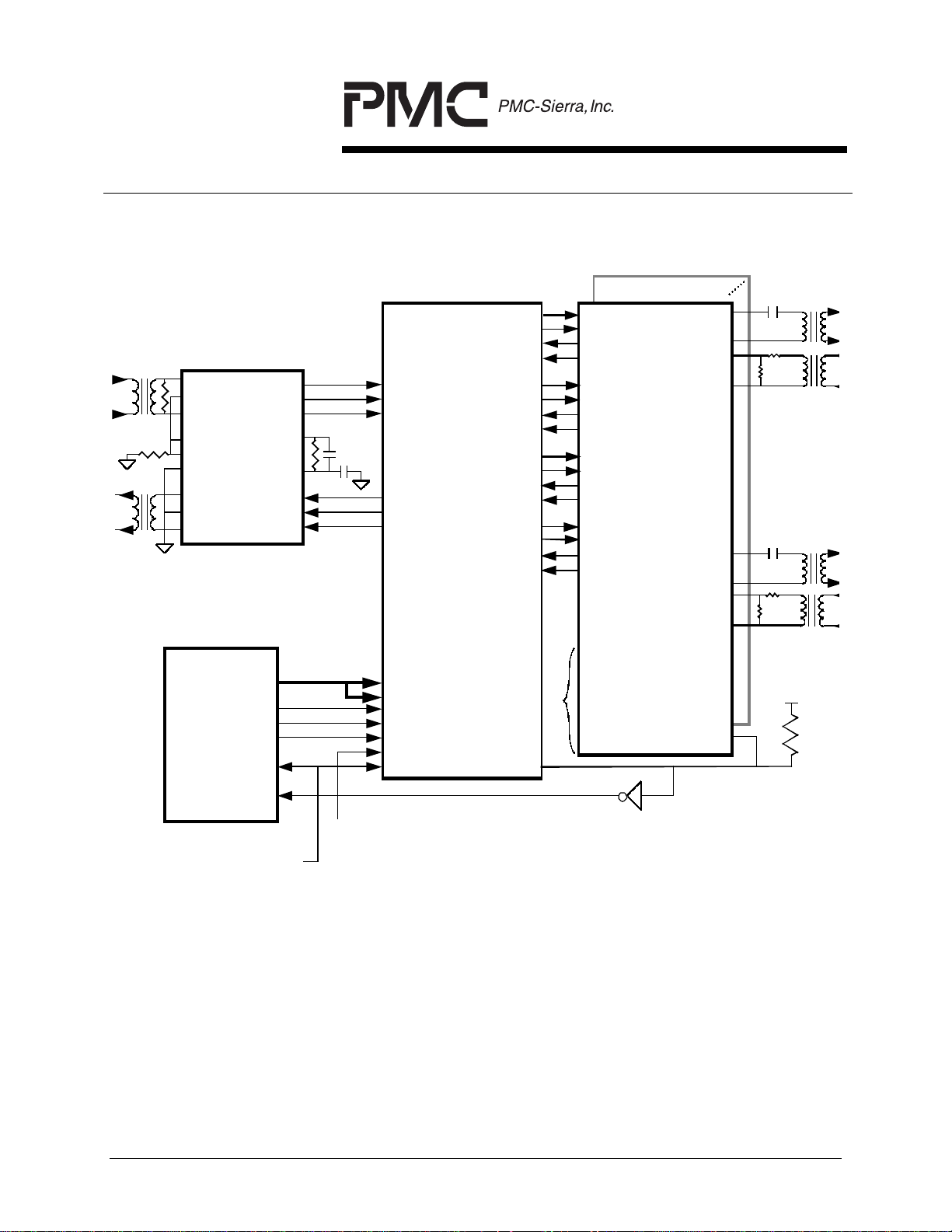
4
APPLICATION EXAMPLES
Figure 1 - Example 1. T1 or E1 ATM Interfaces
SCI-PHY
Multi-PHY
ATM Cell Bus
Generic
Microprocessor
Bus
1X Transmit Reference Clock
DSX-1
PM7344
S/UNI-MPH
Q u a d T1 /E 1
TM
Multi-P HY
Us er Ne tw o r k I n te r fa c e
PM4314
QDSX
Quad T1/E1
Line In terfa c e Dev ic e
Crystal Oscillator 24X Clock
(37.056 MHz for T1 or 49.152 MHz
for E1) if using jitter attenuator or
XPL S W IDEN fun ction . 8 X c loc k
otherwise.
or
E1
Analog
Interfaces
Example 1 shows the PM4314 QDSX used with the PM7344 S/UNI-MPH to
implement a quad T1/E1 UNI where the DS1 or E1 signals are presented on
DSX-1 or E1 electrical interfaces.
In this example, the DSX-1 or E1 line interface functions are provided by the
QDSX and the DS-1 or E1 framing functions are provided by the S/UNI-MPH.
The S/UNI-MPH also provides the ATM cell processing functions associated with
the PHY layer, including the implementation of a SCI-PHY multi-PHY interface to
the ATM layer device(s). The combination of the QDSX device with the S/UNIMPH allows both ANSI/ITU compliant DSX-1/E1 analog signals and ATM Forum
UNI 3.1 and ITU G.804 compliant DS1/E1 digital signals to be processed.
Jitter attenuation by both the QDSX and the S/UNI-MPH can be performed by
supplying a 24X reference clock to the devices. If jitter attenuation is to be
executed by the S/UNI-MPH only, then an 8X reference clock is required by the
QDSX and a 24X reference clock is required by the S/UNI-MPH. If jitter
attenuation is to be executed by the QDSX, then a 24X reference clock must be
PROPRIETARY AND CONFIDENTIAL TO PMC-SIERRA, INC., AND FOR ITS CUSTOMERS’ INTERNAL USE
8
Page 21

PM4314 QDSX
DATA SHEET
PMC-950857 ISSUE 5 QUAD T1/E1 LINE INTERFACE DEVICE
supplied to it and an 8X reference clock may be supplied to the S/UNI-MPH. If
jitter attenuation is not required by either device, then an 8X reference clock may
be supplied to both devices.
PROPRIETARY AND CONFIDENTIAL TO PMC-SIERRA, INC., AND FOR ITS CUSTOMERS’ INTERNAL USE
9
Page 22
PM4314 QDSX
DATA SHEET
PMC-950857 ISSUE 5 QUAD T1/E1 LINE INTERFACE DEVICE
Figure 2 - Example 2. DSX-1 Digital Access Cross Connects (DACs)
ulse
ame P
m Fr
4.096MHz
Syste
Glue logic can be implemented
using one 74 H C T0 0 an d on e
74HCT175 pack.
D
Q
QB
D
Q
QB
tch
37.056 MHz
Clock
XCLK
D
2.048MHz
BRFPI
BRCLK
Q
QB
BRSIG[1]
BRFPO[1]
BRPCM[1]
BRPCM[2]
BRSIG[3]
BRSIG[2]
BRFPO[3]
BRFPO[2]
BRPCM[4]
BRPCM[3]
IN[0]
IN[1]
IN[2]
IN[3]
IN[4]
IN[5]
IN[6]
IN[7]
FP
CLK2X
BRSIG[4]
BRFPO[4]
Swi
ace
/Sp
Time
OUT[0]
OUT[1]
OUT[2]
OUT[3]
OUT[4]
OUT[5]
OUT[6]
OUT[7]
]
]
[1]
TCLK I[1
BTSIG
BTPCM[1
]
]
]
[1]
[2]
BTFP[1
TCLK I[2
BTCLK
BTSIG
BTPCM[2
]
]
]
[2]
[3]
BTFP[2
TCLK I[3
BTSIG
BTCLK
BTPCM[1
]
]
[3]
BTFP[3
BTCLK
]
]
TCLK I[4
[4]
[4]
BTFP[4
BTSIG
BTCLK
BTPCM[4
PM4344 TQUAD
RDN/RLCV[1]
RCL KI[1]
RDP/RDD[1]
P[1]
RCLKO[1]
RDD/RDP/SD
RLCV/RDN/SDN[1]
1]
RXTIP[
RXRING[1]
RCL K I[2 ]
RDN/RLCV[2]
RDP/RDD[2]
P[2]
RCLKO[2]
RDD/RDP/SD
RLCV/RDN/SDN[2]
2]
RXTIP[
RXRING[2]
RCL K I[3 ]
RDN/RLCV[3]
RDP/RDD[3]
P[3]
RCLKO[3]
RDD/RDP/SD
RLCV/RDN/SDN[3]
3]
RXTIP[
RXRING[3]
RCL K I[4 ]
RDN/RLCV[4]
RDP/RDD[4]
P[4]
RCLKO[4]
RDD/RDP/SD
RLCV/RDN/SDN[4]
4]
RXTIP[
RXRING[4]
XCLK
CLKO8X
PM4314
QDSX
]
DP[1
TDD/T
TDN[1]
]
DP[1
TDD/T
]
P[1
TXTI
]
]
DP[2
TDD/T
TCLKO [1
]
TCLKI[1
TDN[2]
]
DP[2
TDD/T
]
P[2
TXTI
TXRING [1]
]
]
DP[3
TCLKO [2
]
TCLK I[2
TXRING [2]
TDN[3]
TDD/T
]
DP[3
TDD/T
]
P[3
TXTI
]
]
TCLKO [3
]
TCLK I[3
TXRING [3]
]
DP[4
TDN[4]
TDD/T
TCLKO [4
]
]
DP[4
TCLK I[4
TDD/T
]
P[4
TXTI
TXRING [4]
*note:
RC a ttenuation
networks not s h o w n
PROPRIETARY AND CONFIDENTIAL TO PMC-SIERRA, INC., AND FOR ITS CUSTOMERS’ INTERNAL USE
10
Page 23

PM4314 QDSX
DATA SHEET
PMC-950857 ISSUE 5 QUAD T1/E1 LINE INTERFACE DEVICE
Example 2 shows a DSX 1/0 Cross-Connect using a PM4314 QDSX, a PM4344
TQUAD, and a Digital Time/Space Switch to implement a simple 1/0 crossconnect. An alternate architecture could use two Digital Time/Space Switches,
one as a voice switch and the other as a signaling switch, and 2 TQUADs to
cross-connect eight T1s. (Note: a true implementation would require redundancy
in the switch core.)
In this example, the TQUAD is programmed to receive and generate the same
framing format, using the 2.048 MHz backplane data rate. The "system frame
pulse" signal is stretched through the two D-FF into a pulse of 488ns duration,
which is used to frame align the data out of each framer through the elastic store
and to provide frame alignment indication to the transmitters. The raw system
frame pulse signal is used to indicate frame alignment synchronization to the
Digital Time/Space Switch. Another D-FF is configured as a toggle to generate a
2.048MHz clock from the system 4.096MHz clock source, synchronized to the
system frame pulse. The TQUAD is configured to accept and source unipolar
signal from and to the QDSX. As shown, the jitter attenuation is performed in the
QDSX and is disabled in the TQUAD.
PROPRIETARY AND CONFIDENTIAL TO PMC-SIERRA, INC., AND FOR ITS CUSTOMERS’ INTERNAL USE
11
Page 24
PM4314 QDSX
DATA SHEET
PMC-950857 ISSUE 5 QUAD T1/E1 LINE INTERFACE DEVICE
Figure 3 - Example 3. Multiplexers (M13)
(7 Quad DSX-1/E1 line interfaces)
LIN+
NC-R
LIN-
RGND
RFO
TGN D
LOUT+
NC-T
LOUT-
P
µ
0
0
2
7
8P
I 7
SS
DS-3 Line Interfa ce
AD[15:0]
ALE
RDB
WR B
RESB
RPOS
RNEG
RCL K
LF1
LF2
TPOS
TNE G
TCL K
RPOS
RNEG
RCLK
TPOS
TNEG
TCLK
TICLK
TOH
TOHEN
TIMFP
TOHCLK
TOHFP
A[8:0]
D[7:0]
ALE
RDB
WRB
CSB
RSTB
PM83 13
MX
D3
r
e
lex
tip
ul
M
3
M1
RD1DAT1
RD1CLK1
TD1DAT1
TD1CLK1
RD1DAT2
RD1CLK2
TD1DAT2
TD1CLK2
RD1DAT3
RD1CLK3
TD1DAT3
TD1CLK3
RD1DAT4
RD1CLK4
TD1DAT4
TD1CLK4
RD1DAT28
RD1CLK28
TD1DAT28
TD1CLK28
INTB
•
•
•
•
•
•
•
•
•
1:1.36
1:2
1:1.36
1:2
+5V
PM43 14
SX
QD
TXTIP[1]
TXRING[1]
RXTIP[1]
RXR ING[1]
TXTIP[2]
TXRING[2]
RXTIP[2]
RXR ING[2]
TXTIP[3]
TXRING[3]
RXTIP[3]
RXR ING[3]
TXTIP[4]
TXRING[4]
RXTIP[4]
RXR ING[4]
INTB
TDD[1]
TCLKI[1]
RDD[1]
RCLKO[1]
TDD[2]
TCLKI[2]
RDD[2]
RCLKO[2]
TDD[3]
TCLKI[3]
RDD[3]
RCLKO[3]
TDD[4]
TCLKI[4]
RDD[4]
RCLKO[4]
•
•
•
•
•
o µP
from /t
A[8:0]
D[7:0]
ALE
RDB
WRB
CSB
RSTB
INT
From chip select
decode circuitry
From Master
reset circuitry
Example 3 shows the use of the PM4314 QDSX with the PM8313 D3MX in an
M13 Multiplexer/Demultiplexer application. Use of the SSI LIU as illustrated
requires that TICLK of the D3MX has a duty cycle of 45% min., 55% max. or
better (e.g.. using a Connor Winfield S65T3 reference oscillator).
PROPRIETARY AND CONFIDENTIAL TO PMC-SIERRA, INC., AND FOR ITS CUSTOMERS’ INTERNAL USE
12
Page 25
PM4314 QDSX
DATA SHEET
PMC-950857 ISSUE 5 QUAD T1/E1 LINE INTERFACE DEVICE
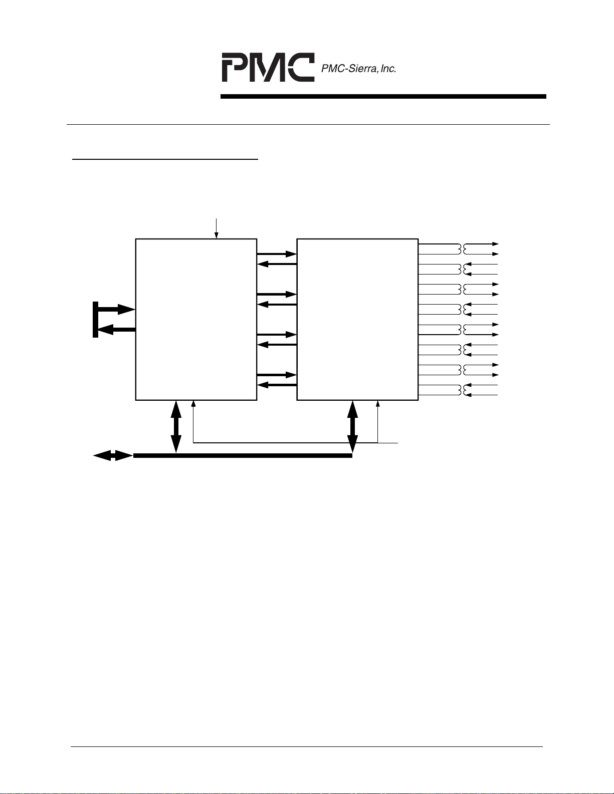
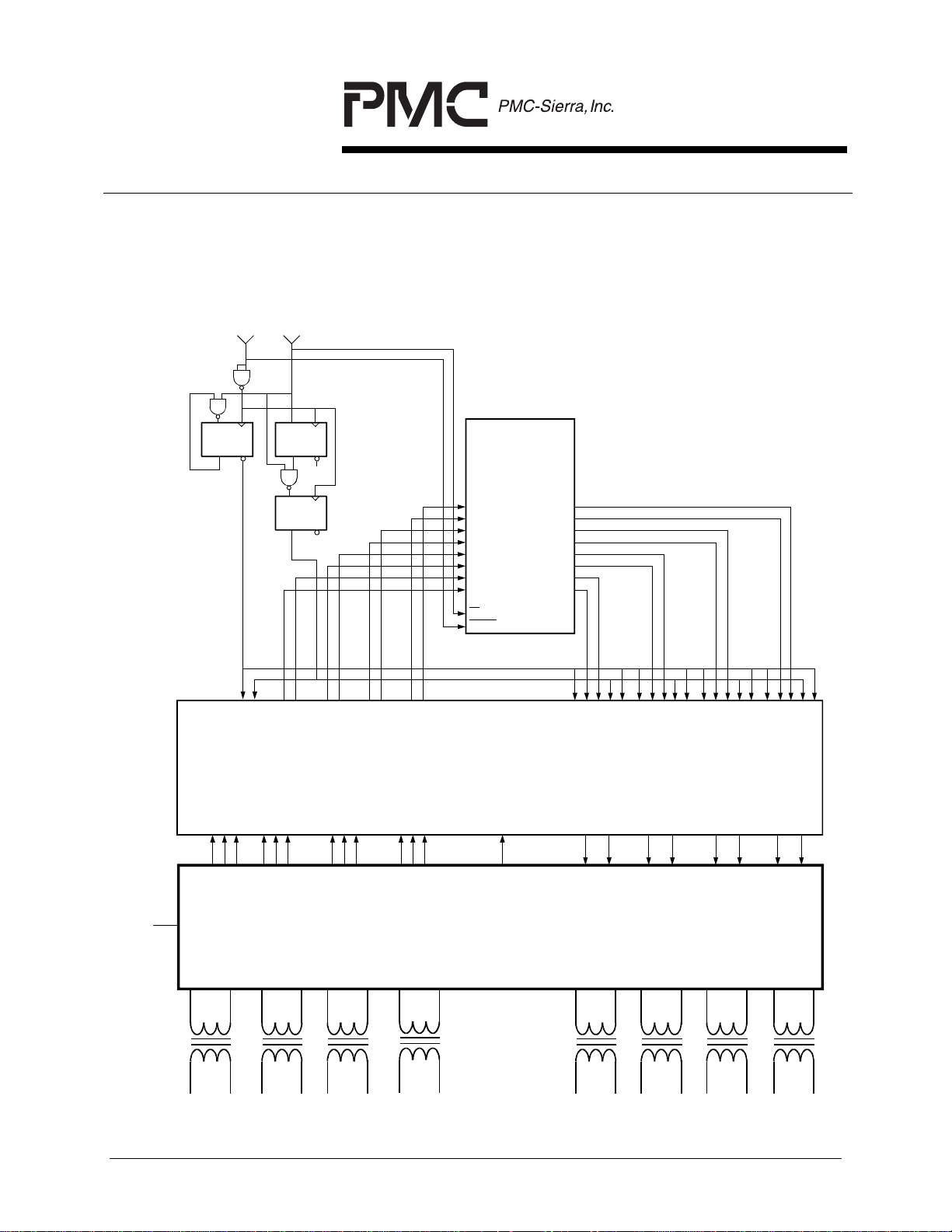
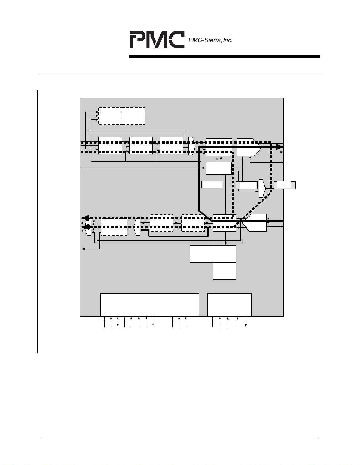
5
BLOCK DIAGRAM
Figure 4 - Normal Operating Mode
TDD/TDP[4:1]
TDN[4:1]
TCLKI[4:1]
XCLK/VCL K
RDD/RDP/SDP[4:1]
RLCV/RDN/SDN[4:1]
PRSM
PRBS
DETECTOR AND
ERROR COUNTER
PRS G
PRBS
GENERA TOR
DJAT
DIGITAL JITTER
ATTENUAT OR
IBC D
IN-BAND LOOP-
BACK C ODE
DETECTOR
XIBC
IN-BAND LOOP-
BACK C ODE
GENERA TOR
AM I/B8Z S/HD B3
ENC ODER
XIBC
IN-BAND LOOP-
BACK C ODE
GENERATOR
LCODE
LINE
PRS G
PRBS
GENERATOR
DJAT
DIGITAL JITTER
ATTENUAT OR
TOPS
TIMING OPTIONS
CDRC
CLO C K AN D
DATA
RECOVERY
TRANSMITTER
XPLS
ANA LOG
PULSE
GENERAT OR
RECEIVER
RSLC
ANALOG
PUL SE
SLICER
TXTIP[4:1]
TXR ING[4 :1]
TC[4:1 ]
CLKO8X/CLKO1X
RXTIP[4:1]
RXRING[4:1]
RC[4:1]
RCLKO[4:1]
IBC D
IN-BAND LOOP-
BACK C ODE
DETECTOR
CONTROL SIGNALS
Microprocess or Interface or
Hardware Control Signals
]
:0
[8
WRB
A
D[7:0]
RSTB
DB
R
B
CS
E
TB
L
A
IN
L
AL
TDU
RDUA
R
C
D
LCV_PMON
LINE CODE
VIOLATION
COUNTER
PRSM
PRBS
DETECTOR AND
ERROR COUNTER
BOUND ARY SCAN
IEEE P1149.1
JTAG Test
Access Port
I
B
ST
TR
S
M
T
TD
O
TCK
TD
Note:
Dashed boxes show optional placement of blocks. Default placement of the
block is shown in solid boxe s.
PROPRIETARY AND CONFIDENTIAL TO PMC-SIERRA, INC., AND FOR ITS CUSTOMERS’ INTERNAL USE
13
Page 26
PM4314 QDSX
g
DATA SHEET
PMC-950857 ISSUE 5 QUAD T1/E1 LINE INTERFACE DEVICE
Figure 5 - Loopback Modes
TDD /TDP[4:1]
TDN[4:1]
TCLKI[4:1]
XCL K/VCLK
RDD/RDP/SDP[4:1]
RLCV/RDN/SDN[4:1]
RCLKO[4:1]
PRSM
PRBS
DETECTOR AND
ERROR COUNTER
PRSG
PRBS
GENERATOR
DJAT
DIGITAL JITTER
ATTENU ATOR
IBCD
IN-BAND LOOP-
BACK CODE
DETECTOR
XIBC
IN-BAND LOOP-
BACK CODE
GENERATOR
LCODE
AMI/B8ZS/H DB3
ENCODER
XIBC
IN-BAND LOOP-
BACK CODE
GENERATOR
LIN E
PRSG
PRBS
GENERATOR
IN-BAND LOOP-
BACK CODE
DETECTOR
LINELB
IBCD
DJAT
DIGITAL JITTER
ATTENUATOR
TOPS
TIMING OPTIONS
CDRC
CLOCK AN D
DATA
RECOVERY
LCV_PMON
LINE CODE
VIOLATION
COUNTER
PRSM
PRBS
DETECTOR AND
ERROR COUNTER
TRANSMITTER
XPL S
ANALOG
PULSE
GENERAT OR
DIALB
RECEIVER
RSLC
ANA LOG
PULSE
SLICER
TXTIP[4:1]
TXRING[4:1 ]
TC[4:1]
DMLB
CLKO8X/CLKO1X
RXTIP[4:1]
RXRING[4:1]
RC[4:1]
CONTROL SIGNALS
Microprocessor Interface or
Hardw are Control Si
]
B
:0
8
A[
RST
B
0]
D[7:
SB
D
R
C
WRB
nals
E
AL
INTB
L
UA
RD
R
C
D
TDU AL
BOUNDAR Y SCAN
IEEE P1149.1
JTAG Test
Access Port
S
K
M
TDI
TC
T
TRSTB
TDO
Note:
Dashed boxes show optional placement of blocks. Default placement of the
block is shown in solid boxe s.
PROPRIETARY AND CONFIDENTIAL TO PMC-SIERRA, INC., AND FOR ITS CUSTOMERS’ INTERNAL USE
14
Page 27

PM4314 QDSX
DATA SHEET
PMC-950857 ISSUE 5 QUAD T1/E1 LINE INTERFACE DEVICE
6
DESCRIPTION
The PM4314 QDSX Quad T1/E1 Line Interface Device is a monolithic integrated
circuit that supports DSX-1 and CEPT E1 compatible transmit and receive
interfaces for four 1.544 Mbit/s or 2.048 Mbit/s data streams.
In the incoming direction, the DSX-1/E1 signals for each quadrant of the QDSX
are first processed by a receive data slicer. The receive data slicer converts the
line signal received via a coupling transformer to dual rail RZ digital pulses.
Adaptation for attenuation is achieved using an integral peak detector that sets
the slicing levels. Through use of passive external attenuation circuitry, either
terminated or bridge monitored DSX-1/E1 signal levels can be accommodated.
The low signal level condition or signal squelch may be enabled to generate
interrupts. Clock and data are recovered from the dual rail RZ digital pulses
using a digital phase-locked loop that provides excellent high frequency jitter
accommodation. The recovered data is decoded using B8ZS, HDB3, or AMI line
code rules and is presented either as a DS-1/E1 stream or presented in an
undecoded dual rail NRZ format. Loss of signal and line code violations are
detected as well as 8 successive zeros/4 successive zeros, and the B8ZS/HDB3
signature. The presence of programmable inband loopback codes is also
detected. These various events or changes in status may be enabled to
generate interrupts. Additionally, line code violations are indicated on outputs.
In the outgoing direction, each quadrant of the QDSX may accept either a DS1/E1 stream to be encoded using B8ZS, HDB3, or AMI line code rules, or it may
accept pre-encoded data in dual rail NRZ format. Jitter attenuation is provided
by passing outgoing data through a FIFO. A low jitter clock is generated by an
integral digital phase-locked loop and is used to read data from the FIFO. FIFO
overrun or underrun may be enabled to generate interrupts. Alarm indication
signal (all ones) may be substituted for the FIFO data. The digital data is
converted to high drive, dual rail RZ pulses that drive the DSX-1/E1 interface
through a coupling transformer. The shape of the pulses is user programmable
to ensure that the DSX-1/E1 pulse template is met after the signal is passed
through different cable lengths or types. Driver performance monitoring is
provided and may be enabled to generate interrupts upon driver failure.
The jitter attenuation function can optionally be moved to the receive side. The
recovered clock and data is passed through the jitter attenuator before being
presented at the digital receive outputs.
PROPRIETARY AND CONFIDENTIAL TO PMC-SIERRA, INC., AND FOR ITS CUSTOMERS’ INTERNAL USE
15
Page 28

PM4314 QDSX
DATA SHEET
PMC-950857 ISSUE 5 QUAD T1/E1 LINE INTERFACE DEVICE
Internal high speed timing for all quadrants of the QDSX is provided by a
common 37.056 MHz or 49.152 MHz master clock. This master clock rate is
required for applications where QDSX provides jitter attenuation. For
applications where QDSX is not required to attenuate jitter, a 12.352 MHz or
16.384 MHz clock may be used as the master clock and used directly as the
internal 8X high speed clock.
Diagnostic loopback is provided and the loopback may be invoked past the
analog transmit outputs using the driver performance monitors or invoked prior to
the conversion to analog. Line loopback with jitter attenuation is provided and
may be enabled for automatic operation based on detected inband loopback
codes.
The QDSX detects framed or unframed inband loopback code sequences from
the received input pulses. Any arbitrary code from three to eight bits in length
can be declared to be the activate and deactivate codes by writing to
configuration registers. The inband loopback code detector can optionally be
moved to the transmit side where it detects inband loopback codes in the
unipolar input transmit data stream. For framed inband loopback code
sequences, it is expected that the framing bit overwrites the inband loopback
code bit.
The QDSX may insert unframed inband loopback code sequences into the
transmitted PCM data stream. These codes consist of continuous repetitions of
specific bit sequences. Any arbitrary code from three to eight bits in length is
programmable by writing to configuration registers. This unframed inband
loopback code insertion may optionally be switched to the receive side where it
overwrites the data from the slicer.
The QDSX may insert an unframed 215-1 O.151 compatible pseudo-random bit
sequence into the transmitted PCM data stream. Optionally, the PRBS insertion
may be switched to the receive side where it overwr ites the data from the slicer.
The QDSX detects an unframed 215-1 O.151 compatible pseudo-random bit
sequence input to the receive slicer. This PRBS detector can operate in the
presence of a 10-2 bit error rate. Bit errors are detected and recorded. The
PRBS detector can optionally be switched to the transmit side where it can
detect unframed PRBS data from the unipolar input transmit data stream.
The QDSX operates in conjunction with external line coupling transformers,
resistors, and capacitors. An external crystal may be used for high speed timing
PROPRIETARY AND CONFIDENTIAL TO PMC-SIERRA, INC., AND FOR ITS CUSTOMERS’ INTERNAL USE
16
Page 29

PM4314 QDSX
DATA SHEET
PMC-950857 ISSUE 5 QUAD T1/E1 LINE INTERFACE DEVICE
generation. The QDSX is configured, controlled, and monitored using registers
that are accessed via a generic microprocessor interface.
PROPRIETARY AND CONFIDENTIAL TO PMC-SIERRA, INC., AND FOR ITS CUSTOMERS’ INTERNAL USE
17
Page 30
PM4314 QDSX
DATA SHEET
PMC-950857 ISSUE 5 QUAD T1/E1 LINE INTERFACE DEVICE
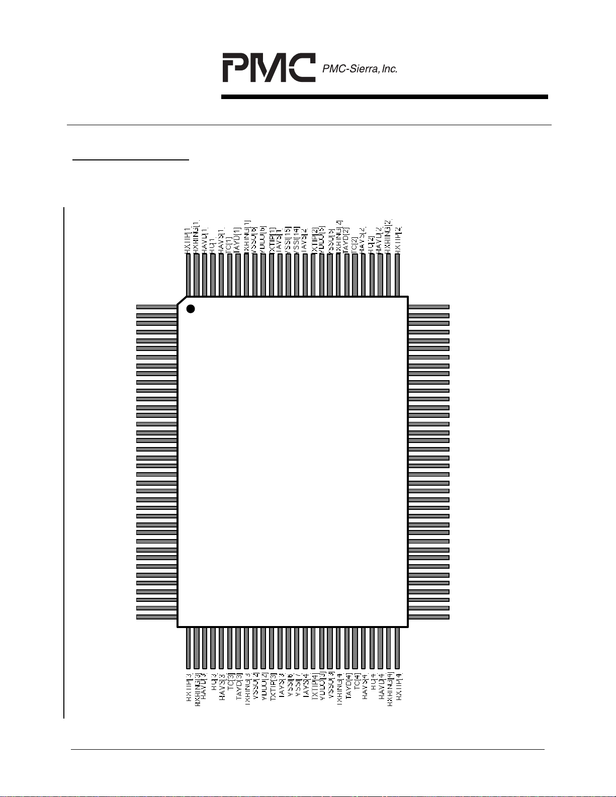
7
PIN DIAGRAM
The QDSX is packaged in a 128-pin plastic QFP package having a body size of
1mm by 20mm and a pin pitch of 0.5 mm.
PIN 128 PIN 103
PIN 1
VSSI[1]
TRSTB
RSTB
VDD0[1]
VSSO[1]
VDDI[1]
VSSI[2]
VSSI[3]
VSSI[4]
VDDI[3]
VSSI[5]
TDI
TCK
TMS
TDO
ALE
CSB
WRB
RDB
INTB
D[0]
D[1]
D[2]
D[3]
D[4]
D[5]
D[6]
D[7]
A[0]
A[1]
A[2]
A[3]
A[4]
A[5]
A[6]
A[7]
A[8]
DCR
Index Pin
PM4314
QD SX
Top
View
PIN 102
VSSI[13]
RDUAL
RDD[1]/RDP[1]/SDP[1]
RLCV[1]/RDN[1]/SDN[1]
RCLKO[1]
RDD[2]/RDP[2]/SDP[2]
RLCV[2]/RDN[2]/SDN[2]
RCLKO[2]
VDDO[4]
VSSO[4]
RDD[3]/RDP[3]/SDP[3]
RLCV[3]/RDN[3]/SDN[3]
RCLKO[3]
RDD[4]/RDP[4]/SDP[4]
RLCV[4]/RDN[4]/SDN[4]
RCLKO[4]
CLKO8X/CLK01X
Reserved
VDDI[2]
VSSI[12]
VSSI[11]
VSSI[10]
VSSI[9]
XCLK/VCLK
TCLKI[1]
TDD[1]/TDP[1]
TDN[1]
TCLKI[2]
TDD[2]/TDP[2]
TDN[2]
TCLKI[3]
TDD[3]/TDP[3]
TDN[3]
TCLKI[4]
TDD[4]/TDP[4]
TDN[4]
TDUAL
VSSI[8]
PIN 38
PIN 65
PIN 39
PROPRIETARY AND CONFIDENTIAL TO PMC-SIERRA, INC., AND FOR ITS CUSTOMERS’ INTERNAL USE
PIN 64
18
Page 31

PM4314 QDSX
DATA SHEET
PMC-950857 ISSUE 5 QUAD T1/E1 LINE INTERFACE DEVICE
8
PIN DESCRIPTION
Pin Name
Type Pin
Function
No.
TXTIP[4]
TXTIP[3]
TXTIP[2]
TXTIP[1]
Output 54
49
113
118
Transmit Bipolar Tip (TXTIP[4:1]). The TXTIP[4:1]
outputs are the transmit analog positive pulses.
These analog outputs drive an AC signal through
an external matching transformer. They must be
connected to the positive lead of the transformer
primary.
An analog Transmit Monitor Positive point is
internally bonded to each of these outputs and is
used to monitor the positive pulses on each
transmit line.
TXRING[4]
TXRING[3]
TXRING[2]
TXRING[1]
Output 57
46
110
121
Transmit Bipolar Ring (TXRING[4:1]). The
TXRING[4:1] outputs are the transmit analog
negative pulses. These analog outputs drive an
AC signal through an external matching
transformer. They must be connected to the
negative lead of the transformer primary.
TC[4]
TC[3]
TC[2]
TC[1]
I/O 59
44
108
123
An analog Transmit Monitor Negative point is
internally bonded to each of these outputs and is
used to monitor the negative pulses on each
transmit line.
Transmit Reference Decoupling Capacitor
(TC[4:1]). These analog bidirectionals provide
decoupling for an internal reference generator.
They must be connected to an external
decoupling capacitor to the corresponding
TAVD[4:1].
PROPRIETARY AND CONFIDENTIAL TO PMC-SIERRA, INC., AND FOR ITS CUSTOMERS’ INTERNAL USE
19
Page 32

PM4314 QDSX
DATA SHEET
PMC-950857 ISSUE 5 QUAD T1/E1 LINE INTERFACE DEVICE
Pin Name
TDD[4]
TDD[3]
TDD[2]
TDD[1]
TDP[4]
TDP[3]
TDP[2]
TDP[1]
TDN[4]
TDN[3]
TDN[2]
TDN[1]
Type Pin
Function
No.
Input 68
71
74
77
Transmit Data (TDD[4:1]). When in single-rail
mode, these inputs are the NRZ data signals to
be transmitted. These inputs can be configured
to be active high or active low. These inputs can
be sampled on either the rising or falling edges of
the corresponding TCLKI[4:1].
Input Transmit Positive Data (TDP[4:1]). When in dual-
rail mode, these inputs are the NRZ positive data
signals to be transmitted. These inputs can be
sampled on either the rising or falling edges of
the corresponding TCLKI[4:1].
Input 67
70
73
76
Transmit Negative Data (TDN[4:1]). When in
dual-rail mode, these inputs are the NRZ
negative data signals to be transmitted. These
inputs can be sampled on either the rising or
falling edges of the corresponding TCLKI[4:1].
These input pins are ignored if the device is
configured for single-rail (unipolar) transmit mode.
TCLKI[4]
TCLKI[3]
TCLKI[2]
TCLKI[1]
RXTIP[4]
RXTIP[3]
RXTIP[2]
RXTIP[1]
RXRING[4]
RXRING[3]
RXRING[2]
RXRING[1]
Input 69
72
75
78
Input 64
39
103
128
I/O 63
40
104
127
Transmit Clock (TCLKI[4:1]). This clock should be
1.544 MHz for DS1 or 2.048 MHz for E1 data
streams and is used to sample the corresponding
TDP/TDD[4:1] and TDN[4:1] signals.
Receive Bipolar Tip (RXTIP[4:1]). The
RXTIP[4:1] inputs are the receive analog positive
pulses. They must be connected to the positive
lead of the transformer secondary through a
passive attenuation network.
Receive Bipolar Ring (RXRING[4:1]). The
RXRING[4:1] bidirectional pins provide DC bias
to an external isolation transformer. They must
be connected to the negative lead of the
transformer secondary and to a decoupling
capacitor to RAVS[4:1].
PROPRIETARY AND CONFIDENTIAL TO PMC-SIERRA, INC., AND FOR ITS CUSTOMERS’ INTERNAL USE
20
Page 33

PM4314 QDSX
DATA SHEET
PMC-950857 ISSUE 5 QUAD T1/E1 LINE INTERFACE DEVICE
Pin Name
RC[4]
RC[3]
RC[2]
RC[1]
RDD[4]
RDD[3]
RDD[2]
RDD[1]
RDP[4]
RDP[3]
RDP[2]
RDP[1]
Type Pin
Function
No.
I/O 61
42
106
125
Receive Peak Hold R-C Network (RC[4:1]). The
RC[4:1] analog bidirectional pins must be
connected to an external parallel
resistor/capacitor network to RAVS[4:1]. This
network is necessary to the operation of the
internal peak detector that tracks the incoming
signal level.
Output 89
92
97
100
Receive Digital Data (RDD[4:1]). When
configured for unipolar output s, the RDD[4: 1]
NRZ outputs contain the sampled DS-1 or E1
data which has been decoded by AMI, B8ZS, or
HDB3 line code rules. RDD[4:1] outputs can be
updated on either the falling or rising RCLKO[4:1]
edge.
Output Receive Digital Positive Pulse (RDP[4:1]). When
configured for bipolar outputs, the RDP[4:1] NRZ
outputs contain sampled bipolar positive pulses.
RDP[4:1] outputs can be updated on either the
falling or rising RCLKO[4:1] edge.
SDP[4]
SDP[3]
SDP[2]
Output Sliced Positive Line Pulse (SDP[4:1]). A positive
pulse on the SDP[4:1] outputs corresponds to the
sampled positive pulse excursion on the
RXTIP[4:1] input.
SDP[1]
PROPRIETARY AND CONFIDENTIAL TO PMC-SIERRA, INC., AND FOR ITS CUSTOMERS’ INTERNAL USE
21
Page 34

PM4314 QDSX
DATA SHEET
PMC-950857 ISSUE 5 QUAD T1/E1 LINE INTERFACE DEVICE
Pin Name
RLCV[4]
RLCV[3]
RLCV[2]
RLCV[1]
RDN[4]
RDN[3]
RDN[2]
RDN[1]
SDN[4]
SDN[3]
SDN[2]
SDN[1]
Type Pin
Function
No.
Output 88
91
96
99
Receive Line Code Violation Indication
(RLCV[4:1]). When configured for unipolar
outputs, the RLCV[4:1] NRZ outputs pulse
whenever a line code violation or excess zeroes
condition is detected. RDP[4:1] outputs can be
updated on either the falling or rising RCLKO[4:1]
edge.
Output Receive Digital Positive Pulse (RDN[4:1]). When
configured for bipolar outputs, the RDN[4:1] NRZ
outputs contain sampled bipolar negative pulses.
RDN[4:1] outputs can be updated on either the
falling or rising RCLKO[4:1] edge.
Output Sliced Negative Line Pulse (SDN[4:1]). A positive
pulse on the SDN[4:1] outputs corresponds to the
sampled negative pulse excursion on the
RXTIP[4:1] input.
RCLKO[4]
RCLKO[3]
RCLKO[2]
RCLKO[1]
Output 87
90
95
98
Recovered Clock Output (RCLKO[4:1]).
RCLKO[4:1] is the clock recovered from the
RXTIP[4:1] and RXRING[4:1] input signals.
RCLKO[4:1] are 2mA output pads. Care must be
taken in board layouts to guarantee the integrity
of the clock signals.
XCLK/ Input 79 Crystal Clock Input (XCLK). This signal supplies
the timing reference for the high-speed clocks
required by many portions of the QDSX. When
jitter attenuation is required, XCLK is nominally a
24X clock (37.056 MHz for T1, 49.152 MHz for
E1). When jitter attenuation is not required,
XCLK can be driven by an 8X clock (12.352 MHz
for T1, 16.384 MHz for E1).
VCLK Vector Clock (VCLK). The VCLK signal is used
during QDSX production test to verify internal
functionality.
PROPRIETARY AND CONFIDENTIAL TO PMC-SIERRA, INC., AND FOR ITS CUSTOMERS’ INTERNAL USE
22
Page 35

PM4314 QDSX
DATA SHEET
PMC-950857 ISSUE 5 QUAD T1/E1 LINE INTERFACE DEVICE
Pin Name
Type Pin
Function
No.
CLKO8X/ Output 86 8X Clock Output (CLKO8X).
This output is the internal 8X high-speed clock
derived from the digital jitter attenuator, or
derived by dividing down the 24X XCLK input. It
is used as the reference clock to generate the
transmit analog pulse template. The CLKO8X
signal is generated from Quadrant 1.
1X Clock Output (CLKO1X).
CLKO1X Output When an 8X clock is provided on XCLK, this is
the internal 8X clock divided by 8. This output
can be used to synchronously clock in data on
TDP[4:1]/TDD[4:1] and TDN[4:1] by connecting it
to TCLKI[4:1].
DCR Input 37 Disable Clock Recove ry Input (DCR). When set
high, the DCR input will disable clock recovery in
the QDSX and enable the SDP[4:1] and SDN[4:1]
sliced line pulse outputs. This input is logically
"ORed" with the DCR register bits.
TDUAL Input 66 Transmit Dual-Rail Input Select (TDUAL). This
input selects whether the QDSX expects single-
rail or dual-rail input transmit data. The TDUAL
input is logically "ORed" with the TDUAL register
bits. When TDUAL is set high, the TDP[4:1] and
TDN[4:1] inputs are enabled. When both the
TDUAL input pin and register bits are set low,
then the TDD[4:1] inputs are enabled and the
TDN[4:1] inputs are ignored.
PROPRIETARY AND CONFIDENTIAL TO PMC-SIERRA, INC., AND FOR ITS CUSTOMERS’ INTERNAL USE
23
Page 36

PM4314 QDSX
DATA SHEET
PMC-950857 ISSUE 5 QUAD T1/E1 LINE INTERFACE DEVICE
Pin Name
Type Pin
Function
No.
RDUAL Input 101 Receive Dual-Rail Output Select (RDUAL). This
input selects whether the QDSX generates
single-rail or dual-rail outputs from its receiver
section. The RDUAL input is logically "ORed"
with the RDUAL register bits. When RDUAL is
set high, the RDP[4:1] and RDN[4:1] outputs are
enabled. When both the RDUAL input pin and
register bits are set low, then line decoding is
performed on the receive slicer outputs and the
RDD[4:1] and RLCV[4:1] outputs are enabled.
The state of the DCR input pin or the DCR
register bits takes precedence over the RDUAL
state.
CSB Input 9 Active low Chip Select (CSB). This signal must be
low to enable QDSX register accesses. CSB
must go high at least once after a powerup to
clear internal test modes. If CSB is not used,
then it should be tied to an inverted version of
RSTB, in which case RDB and WRB determine
register access.
WRB Input 10 Active low Write Strobe (WRB). This signal is
pulsed low to enable a QDSX register write
access. The D[7:0] bus is clocked into the
addressed register on the rising edge of WRB
while CSB is low.
RDB Input Active low Read Enable (RDB). This signal is
pulsed low to enable a QDSX register read
access. The QDSX drives the D[7:0] bus with the
contents of the addressed register while RDB
and CSB are both low.
PROPRIETARY AND CONFIDENTIAL TO PMC-SIERRA, INC., AND FOR ITS CUSTOMERS’ INTERNAL USE
24
Page 37

PM4314 QDSX
DATA SHEET
PMC-950857 ISSUE 5 QUAD T1/E1 LINE INTERFACE DEVICE
Pin Name
Type Pin
Function
No.
A[8]
A[7]
A[6]
A[5]
A[4]
A[3]
A[2]
A[1]
A[0]
Input 35
34
33
32
31
30
29
28
27
Address Bus (A[8:0]). This bus selects specific
registers during QDSX register accesses.
ALE Input 8 Address Latch Enable (ALE). This signal latches
the address bus contents, A[8:0], when low,
allowing the QDSX to be interfaced to a
multiplexed address/data bus. When ALE is high,
the address latches are transparent. ALE has an
integral pull-up resistor.
INTB Output 12 Active low Open-Drain Interrupt (INTB). This
signal goes low when an unmasked interrupt
event is detected on any of the internal interrupt
sources. Note that INTB will remain low until all
active unmasked interrupt sources are
acknowledged at their source.
PROPRIETARY AND CONFIDENTIAL TO PMC-SIERRA, INC., AND FOR ITS CUSTOMERS’ INTERNAL USE
25
Page 38

PM4314 QDSX
DATA SHEET
PMC-950857 ISSUE 5 QUAD T1/E1 LINE INTERFACE DEVICE
Pin Name
Type Pin
Function
No.
D[7]
D[6]
D[5]
D[4]
D[3]
D[2]
D[1]
D[0]
I/O 26
25
24
17
16
15
14
13
Bidirectional Data Bus (D[7:0]). This bus is used
during QDSX read and write accesses.
RSTB Input 7 Active low Reset (RSTB). This signal is set low to
asynchronously reset the QDSX. RSTB is a
Schmitt-trigger input with an integral pull-up
resistor.
TCK Input 3 Test Clock (TCK). This signal provides timing for
test operations that can be carried out using the
IEEE P1149.1 test access port.
TMS Input 4 Test Mode Select (TMS). This signal controls the
test operations that can be carried out using the
IEEE P1149.1 test access port. TMS is sampled
on the rising edge of TCK. TMS has an integral
pull up resistor.
TDI Input 2 Test Data Input (TDI). This signal carries test data
into the QDSX via the IEEE P1149.1 test access
port. TDI is sampled on the rising edge of TCK.
TDI has an integral pull up resistor.
TDO Tristate
Output
6 Test Data Output (TDO). This signal carries test
data out of the QDSX via the IEEE P1149.1 test
access port. TDO is updated on the falling edge
of TCK. TDO is a tristate output which is inactive
except when scanning of data is in progress.
PROPRIETARY AND CONFIDENTIAL TO PMC-SIERRA, INC., AND FOR ITS CUSTOMERS’ INTERNAL USE
26
Page 39

PM4314 QDSX
DATA SHEET
PMC-950857 ISSUE 5 QUAD T1/E1 LINE INTERFACE DEVICE
Pin Name
Type Pin
Function
No.
TRSTB Input 5 Active low Test Reset (TRSTB). This signal
provides an asynchronous QDSX test access
port reset via the IEEE P1149.1 test access port.
TRSTB is a Schmitt triggered input with an
integral pull up resistor. When not being used,
TRSTB should be tied to RSTB.
VDDO[6]
VDDO[5]
VDDO[4]
VDDO[3]
Power 119
112
94
55
Pad Ring Power Pins (VDDO[6:1]). These pins
must be connected to a common well decoupled
+5V DC power supply together with the
VDDI[3:1], TAVD[4:1], and RAVD[4:1] pins. Care
must be taken to avoid coupling noise between
these pins.
VDDO[2]
VDDO[1]
VDDI[3]
VDDI[2]
VDDI[1]
Power 36
48
18
84
20
Core Power Pins (VDDI[3:1]). These pins must be
connected to a common well decoupled +5V DC
power supply together with the VDDO[6:1],
TAVD[4:1], and RAVD[4:1] pins. Care must be
taken to avoid coupling noise between these
pins.
VSSO[6]
VSSO[5]
VSSO[4]
VSSO[3]
VSSO[2]
VSSO[1]
PROPRIETARY AND CONFIDENTIAL TO PMC-SIERRA, INC., AND FOR ITS CUSTOMERS’ INTERNAL USE
Ground 120
111
93
56
47
19
Pad Ring Ground Pins (VSSO[6:1]). These pins
must be connected to a common ground together
with the VSSI[15:1], TAVS[4:1], and RAVS[4:1]
pins. Care must be taken to avoid coupling noise
between these pins.
27
Page 40

PM4314 QDSX
DATA SHEET
PMC-950857 ISSUE 5 QUAD T1/E1 LINE INTERFACE DEVICE
Pin Name
VSSI[15]
VSSI[14]
VSSI[13]
VSSI[12]
VSSI[11]
VSSI[10]
VSSI[9]
VSSI[8]
VSSI[7]
VSSI[6]
VSSI[5]
VSSI[4]
VSSI[3]
Type Pin
No.
Ground 116
115
102
83
82
81
80
65
52
51
38
23
22
Function
Core Ground Pins (VSSI[15:1]). These pins must
be connected to a common ground together with
the VSSO[6:1], TA VS[4:1], and RAVS[4:1]pi ns.
Care must be taken to avoid coupling noise
between these pins. These pins also act as
thermal-dissipation grounds, and as such should
be thermally well-connected to a ground plane.
VSSI[2]
VSSI[1]
TAVD[4]
TAVD[3]
TAVD[2]
TAVD[1]
TAVS[4]
TAVS[3]
TAVS[2]
TAVS[1]
TX
Analog
Power
TX
Analog
Ground
21
1
58
45
109
122
53
50
114
117
Transmit Analog Power Pins (TAVD[4:1]). These
pins provide the +5 V supply to the transmit
analog line interfaces. The transmit analog line
interface remains in a low power consumption
state after reset until enabled. TAVD[4:1] must be
connected to a common well decoupled +5 V DC
power supply together with the VDDO[6:1],
VDDI[3:1], and RAVD[4:1] pins. Care must be
taken to avoid coupling noise between these
pins.
Transmit Analog Ground Pins (TAVS[4:1]). These
pins provide the ground supply to the transmit
analog line interface. TAVS[4:1] must be
connected to a common ground together with the
VSSO[6:1], VSSI[15:1], and RAVS[4:1] pins.
Care must be taken to avoid coupling noise
between these pins.
PROPRIETARY AND CONFIDENTIAL TO PMC-SIERRA, INC., AND FOR ITS CUSTOMERS’ INTERNAL USE
28
Page 41

PM4314 QDSX
DATA SHEET
PMC-950857 ISSUE 5 QUAD T1/E1 LINE INTERFACE DEVICE
Pin Name
Type Pin
No.
RAVD[4]
RAVD[3]
RAVD[2]
RAVD[1]
RAVS[4]
RAVS[3]
RAVS[2]
RAVS[1]
RX
Analog
Power
RX
Analog
Ground
62
41
105
126
60
43
107
124
Notes on Pin Description:
Function
Receive Analog Power Pins (RAVD[4:1]). These
pins provide the +5 V DC power supply to the
receive analog line interface. RAVD[4:1] must be
connected to a common well decoupled +5 V DC
power supply together with the VDDO[6:1],
VDDI[3:1], and TAVD[4:1] pins. Care must be
taken to avoid coupling noise between these
pins.
Receive Analog Ground Pins (RAVS[4:1]). These
pins provide the ground supply to the receive
analog line interface. RAVS[4:1] must be
connected to a common ground together with the
VSSO[6:1], VSSI[15:1], and TAVS[4:1] pins. Care
must be taken to avoid coupling noise between
these pins.
1. VDDI[3:1] and VSSI[15:1] are the +5 V and ground connections, respectively,
for the core circuitry of the device. VDDO[6:1] and VSSO[6:1] are the +5 V
and ground connections, respectively, for the pad ring circuitry of the device.
TAVD[4:1] and TAVS[4:1] are the +5 V and ground connections, respectively,
for the transmit analog circuitry of the device. RAVD[4:1] and RAVS[4:1] are
the
+5 V and ground connections, respectively, for the receive analog circuitry of
the device. These power supply connections must all be utilized and must all
connect to a common +5 V or ground rail, as appropriate. There is no low
impedance connection within the PM4314 QDSX between the core, pad ring,
transmit analog, and receive analog supply rails. Failure to properly make
these connections may result in improper operation or damage to the device.
Care must be taken to avoid coupling of noise into the transmit and receive
analog supply rails.
2. Inputs RSTB, ALE, TMS, TDI, and TRSTB have integral pull-up resistors.
3. All QDSX inputs and bidirectionals present minimum capacitive loading and
operate at TTL logic levels.
PROPRIETARY AND CONFIDENTIAL TO PMC-SIERRA, INC., AND FOR ITS CUSTOMERS’ INTERNAL USE
29
Page 42

PM4314 QDSX
DATA SHEET
PMC-950857 ISSUE 5 QUAD T1/E1 LINE INTERFACE DEVICE
4. All QDSX digital outputs and bidirectionals have 2 mA drive capability. The
data bus outputs, D[7:0], and CLKO8X have 4 mA drive capability. For board
layouts, care should be maken with the 2mA drive RCLKO[4:1] signals to
guarantee clock signal integrity.
5. The recommended power supply sequencing is as follows:
5.1VDDI[3:1] power must be supplied either before VDDO[6:1] or
simultaneously with VDDO[6:1]. Connection of VDDI[3:1] and VDDO[6:1] to a
common VDD power plane is recommended.
5.2The VDDI[3:1] and VDDO[6:1] power must be applied before input pins
are driven or the input current per pin must be limited to less than 20 mA.
5.3Analog power supplies must be applied after both VDDI[3:1] and
VDDO[6:1] have been applied or the they must be current limited to the
maximum latchup current specification. (100 mA). In operation the differential
voltage measured between TAVD[4:1] and RAVD[4:1] supplies and VDDI[3:1]
and VDDO[6:1] must be less than 0.5 volt. The relative power sequencing of
TAVD[4:1] and RAVD[4:1] power supplies is not important.
5.4Power down the device in the reverse sequence.
PROPRIETARY AND CONFIDENTIAL TO PMC-SIERRA, INC., AND FOR ITS CUSTOMERS’ INTERNAL USE
30
Page 43

PM4314 QDSX
DATA SHEET
PMC-950857 ISSUE 5 QUAD T1/E1 LINE INTERFACE DEVICE
9
FUNCTIONAL DESCRIPTION
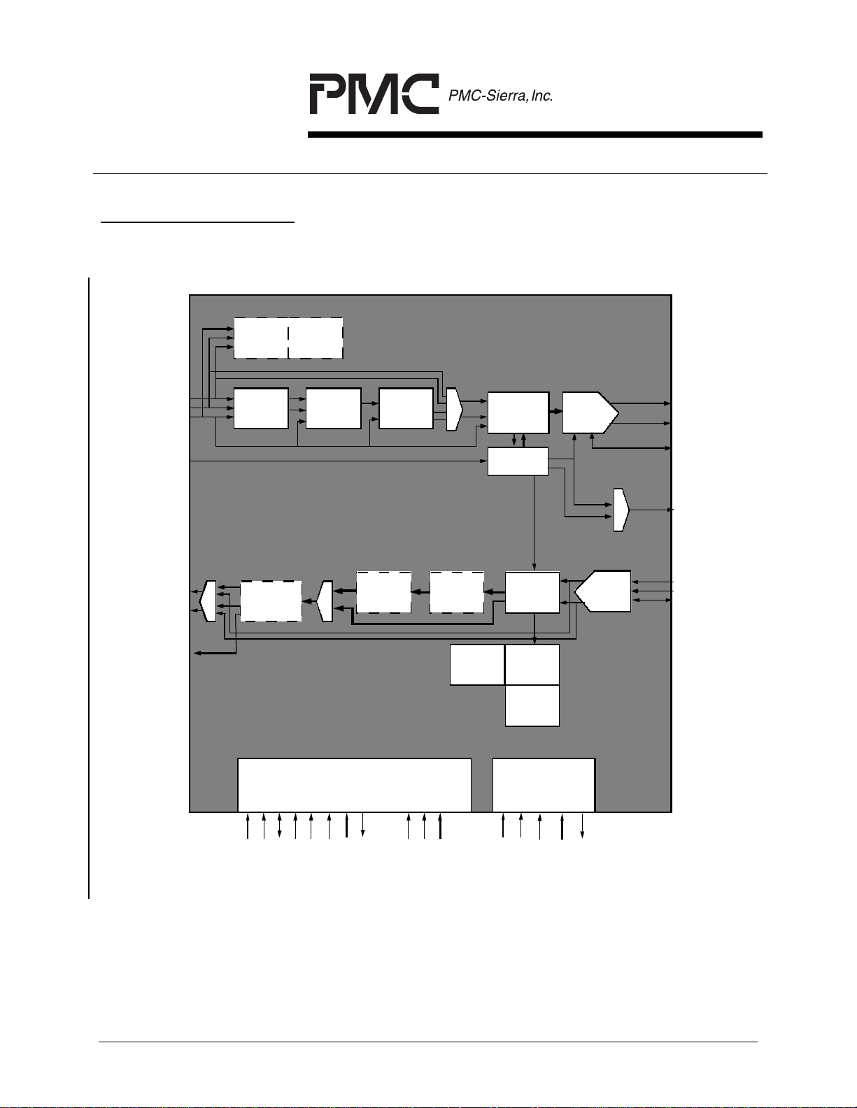
9.1 Analog Pulse Slicer (RSLC)
The Analog T1/E1 Pulse Slicer function is provided by the RSLC block. The
Receive Data Slicer (RSLC) block provides the first stage of signal conditioning
for a G.703 1544kbit/s (DSX-1) or 2048 kbit/s (E1) serial data stream by
converting bipolar line signals to dual rail RZ pulses. Before an RZ output pulse
is generated by the RSLC block, bipolar input signals must rise to 50% (for E1) or
67% (for DSX-1) of their peak amplitude. This level is referred to as the slicing
level. The threshold criteria insures accurate pulse or mark recognition in the
presence of noise.
The RSLC block relies on an external network for compliance to the DSX-1 and
E1 input port specifications. The RSLC block is configured via an off-chip
attenuator pad to operate in one of four modes: DSX-1 normal mode, DSX-1
bridging mode, G.703 120 Ω twisted pair, or G.703 75 Ω coax.
According to G.703, the amplitude of a DSX-1 normal mode received pulse at
the 1:2 line-coupling transformer's primary should be in the range from 3.6V to
1.2V (depending on the length of the cable from the signal source). In this mode,
the QDSX can receive signal levels down to a typical squelching level of 227mV,
leaving a 14.5dB margin between the minimum expected signal level and the
typical minimum receivable signal level.
In DSX-1 bridging mode, the QDSX is connected to a monitor jack which bridges
across the line and attenuates the signal levels by 20 dB, so the expected pulse
amplitude at the 1:2 line-coupling transformer's primary should be in the range
from 360mV to 120mV (depending on the length of the cable from the signal
source). In this mode, the QDSX can receive signal levels down to a squelching
level of 50mV, leaving 7.6 dB margin between the minimum expected signal level
and the typical minimum receivable signal level.
In 120Ω E1 mode, the amplitude of a received pulse at the 1:2 line-coupling
transformer's primary can be in the range from 3.3V to 1.4V (depending on the
length of the cable from the signal source). In this mode, the QDSX can receive
signal levels down to a squelching level of 276mV, which means that there is
14.1 dB margin between the minimum expected signal level and the typcial
minimum receivable signal level.
PROPRIETARY AND CONFIDENTIAL TO PMC-SIERRA, INC., AND FOR ITS CUSTOMERS’ INTERNAL USE
31
Page 44

PM4314 QDSX
DATA SHEET
PMC-950857 ISSUE 5 QUAD T1/E1 LINE INTERFACE DEVICE
In 75Ω E1 mode, the amplitude of a received pulse at the 1:2 line-coupling
transformer's primary can be in the range from 2.6V to 1.1V (depending on the
length of the cable from the signal source). In this mode, the QDSX can receive
signal levels down to a squelching level of 220mV which means that there is
14.0 dB margin between the minimum expected signal level and the minimum
receivable signal level in the worst case.
The RSLC block provides a squelching circuit, which indicates an alarm when
input pulses are below the squelching level threshold. In this state, data is not
sliced, which prevents the detection of noise on an idle transmission line. The
SQ status bit in the RSLC Interrupt Enable/Status registers (031H, 071H, 0B1H,
and 0F1H) goes high whenever the RSLC block is squelching the input signal.
The RSLC can be configured to generate an interrupt whenever the SQ status bit
changes state.
The off-chip attenuator pad network is shown in Figure 6 and the network values
below are recommended for the specified applications:
Table 1 -
Signal Type Turns
Ratio
(N ± 5%)
R1
(Ω ± 1%)R2(Ω ± 1%)
Squelch
Level at
Primary
(mV T ypical)
Zo=120Ω
Zo=75Ω
2 357 121 276CEPT E1
2 205 95.3 220
Normal 2 309 93 227DSX-1
Bridging 2 0 402 50
Tight tolerances are required on the resistors and turns ratio to meet the return
loss specification.
PROPRIETARY AND CONFIDENTIAL TO PMC-SIERRA, INC., AND FOR ITS CUSTOMERS’ INTERNAL USE
32
Page 45

PM4314 QDSX
DATA SHEET
PMC-950857 ISSUE 5 QUAD T1/E1 LINE INTERFACE DEVICE
Figure 6 - External Analog Receive Interface Circuit
V
DD
1:N
T
R1
RXTIP
R2
R
RXRING
RC0.1 µF
± 10%
316 kΩ ±1%
47 nF
±10%
Notes:
1. All capacitors ceramic
2. Some transformer manufacturers produce a dual part containing both the 1:2 & 1:1.36
transformers required for the receive and transmit interfaces, respectively.
RAVD
RAVS
The transformer used should be designed for use in T1/CEPT/ISDN-PRI
applications. Many manufacturers have standard products for these applications.
Typical characteristics of a suitable transformer are given in the following table.
PROPRIETARY AND CONFIDENTIAL TO PMC-SIERRA, INC., AND FOR ITS CUSTOMERS’ INTERNAL USE
33
Page 46

PM4314 QDSX
DATA SHEET
PMC-950857 ISSUE 5 QUAD T1/E1 LINE INTERFACE DEVICE
Table 2 -
Turns
Ratio
OCL (mH
min.)
C
w/w
max.)
(pF
LL (µH
max.)
DCR pri.
(Ω max.)
DCR sec.
(Ω max.)
(PRI:SEC)
1:2 1.20 35 0 .80 0.80 1.2
where OCL is the open-circuit inductance,
C
L
is the inter-winding capacitance,
w/w
is the leakage inductance, and
L
DCR is the DC resistance.
PMC-Sierra has verified the operation of the RSLC functional block with the
following transformers:
• Pulse Engineering PE64931 (1:1:1) and PE64952 (1:2CT)
• BH Electronics 500-1775 (1:1:1) and 500-1777 (1:2CT)
Many manufacturers produce dual transformers containing the 1:2 CT and 1:1.36
transformers necessary for the receiver and transmitter circuits. PMC-Sierra has
verified the operation of XPLS and RSLC with the following dual parts:
• Pulse Engineering PE64952
• Pulse Engineering PE65774 (for extended temperature range)
• BH Electronics500-1777
9.2 Clock and Data Recovery (CDRC)
The Clock and Data Recovery function is contained in the CDRC block and is
active when clock recovery is not disabled. The CDRC provides clock and data
recovery, B8ZS/HDB3 decoding, bipolar violation detection, and loss of signal
detection. It recovers the clock from the incoming RZ data pulses using a digital
phase-locked-loop and recovers the NRZ data. Loss of signal is declared after
exceeding a programmed threshold of 10, 31, 63, or 175 consecutive bit periods
of the absence of pulses on both the positive and negative line pulse inputs and
is removed after the occurrence of a single line pulse. If enabled, a
microprocessor interrupt is generated when a loss of signal is detected and when
the signal returns. When the CDRC is disabled, the positive and negative sliced
PROPRIETARY AND CONFIDENTIAL TO PMC-SIERRA, INC., AND FOR ITS CUSTOMERS’ INTERNAL USE
34
Page 47

PM4314 QDSX
DATA SHEET
PMC-950857 ISSUE 5 QUAD T1/E1 LINE INTERFACE DEVICE
pulses from RSLC are passed directly to the SDP[X] and SDN[X] outputs
respectively.
The input jitter tolerance for DSX-1 interfaces complies with the Bellcore
document TA-TSY-000170 and with the AT&T specification TR 62411. The
tolerance is measured with a QRSS sequence (220-1 with 14 zero restriction).
The CDRC block provides two algorithms for clock recovery that result in differing
jitter tolerance characteristics. The first algorithm (when the ALGSEL register bit
in the CDRC Configuration register (010H, 050H, 090H, 0D0H) is logic 0)
provides good low frequency jitter tolerance, but the high frequency tolerance is
close to the TR 62411 limit. The second algorithm (when ALGSEL is logic 1)
provides much better high frequency jitter tolerance, approaching 0.5UIpp (Unit
Intervals peak-to-peak), at the expense of the low frequency tolerance; the low
frequency tolerance of the second algorithm is approximately 80% of that of the
first algorithm. The DSX-1 jitter tolerance with ALGSEL set to 1 and to 0 is
shown in Figure 7.
PROPRIETARY AND CONFIDENTIAL TO PMC-SIERRA, INC., AND FOR ITS CUSTOMERS’ INTERNAL USE
35
Page 48

PM4314 QDSX
DATA SHEET
PMC-950857 ISSUE 5 QUAD T1/E1 LINE INTERFACE DEVICE
Figure 7 - DSX-1 jitter tolerance
10
IN SPEC. REGION
SINEWAVE
JITTER
AMPLITUDE
P. TO P. (UI)
LOG SCALE
CDRC MAX. TOLERANCE
(ALGSEL=0)
CDRC MAX. TOLERANCE
(ALGSEL=1)
0.4
0.3
AT&T SPEC.
BELLCORE SPEC.
0.31
0.70
SINEWAVE JITTER FREQUENCY, kHz - LOG SCALE
10
The input jitter tolerance for E1 interfaces complies with ITU-T Recommendation
G.823. The tolerance is measured with a 215-1 sequence. The E1 jitter tolerance
with ALGSEL set to 1 and to 0 is shown in Figure 8 and Figure 9.
100
PROPRIETARY AND CONFIDENTIAL TO PMC-SIERRA, INC., AND FOR ITS CUSTOMERS’ INTERNAL USE
36
Page 49

PM4314 QDSX
DATA SHEET
PMC-950857 ISSUE 5 QUAD T1/E1 LINE INTERFACE DEVICE
Figure 8 - E1 jitter tolerance with ALGSEL = 1
Measurement Limit
10
1.0
G823 Jitter
Tolerance
Specification
0.1
Jitter Amplitude (UIp-p)
0.01
10
.
.
100
Jitter Frequency (Hz)
1K
Measured
CDRC Jitter
Tolerance
(ALGSEL = 1)
10K
100K
PROPRIETARY AND CONFIDENTIAL TO PMC-SIERRA, INC., AND FOR ITS CUSTOMERS’ INTERNAL USE
37
Page 50

PM4314 QDSX
DATA SHEET
PMC-950857 ISSUE 5 QUAD T1/E1 LINE INTERFACE DEVICE
Figure 9 - E1 jitter tolerance with ALGSEL = 0
Measurement Limit
10
1.0
G823 Jitter
0.1
Tolerance
Specification
Jitter Amplitude (UIp-p)
0.01
10
.
.
100
Jitter Frequence (Hz)
1K
10K
Measured
CDRC Jitter
Tolerance
(ALGSEL = 0)
100K
9.3 Line Code Violation Performance Monitor (LCV_PMON)
The Line Code Violation Performance Monitor function is provided by the
(LCV_PMON) block. This block accumulates line code violation events with
saturating counters over consecutive intervals as defined by the period of the
supplied transfer clock signal. When the transfer clock signal is applied, the
LCV_PMON block transfers the counter values into holding registers and resets
the counters to begin accumulating events for the interval. The counters are reset
in such a manner that error events occurring during the reset are not missed. If
enabled, an interrupt is generated whenever counter data is transferred into the
holding registers. If the holding registers are not read between successive
transfer clocks, the OVR register bit in the LCV_PMON Interrupt Enable/Status
register (014H, 054H, 094H, and 0D4H) is asserted.
PROPRIETARY AND CONFIDENTIAL TO PMC-SIERRA, INC., AND FOR ITS CUSTOMERS’ INTERNAL USE
38
Page 51

PM4314 QDSX
DATA SHEET
PMC-950857 ISSUE 5 QUAD T1/E1 LINE INTERFACE DEVICE
Generation of the individual LCV_PMON transfer clocks for specific quadrants of
the QDSX is performed by writing to any of the LCV_PMON counter register
locations of the particular quadrant. A global performance monitor transfer clock
signal is generated by writing to register 007H. This will latch the counter values
in all the LCV_PMONs and PRSMs of the QDSX. The holding register
addresses are contiguous to facilitate polling operations.
9.4 Inband Loopback Code Detector (IBCD)
The Inband Loopback Code Detection function is provided by the IBCD block.
This block detects the presence of either of two programmable loopback code
sequences, ACTIVATE and DEACTIVATE, in framed or unframed DS-1 data
streams. The inband code sequences are expected to be overwritten by the
framing bit in framed data streams. Each code sequence is defined as the
repetition of the programmed code in the PCM stream for at least 5.1 seconds.
The code sequence detection and timing is compatible with the specifications
defined in T1.403, TA-TSY-000312, and TR-TSY-000303. ACTIVATE and
DEACTIVATE code indication is provided through internal register bits. An
interrupt is generated to indicate when either code status has changed. The
IBCD can detect inband loopback codes in the recovered unipolar receive data
when configured to be in the receive data stream or in the unipolar input transmit
data when configured to be in the transmit data stream. When enabled in the
receive stream, the IBCD can be configured to enable and disable line loopback
on detection of inband loopback activate and deactivate sequences.
9.5 Pseudo-Random Bit Sequence Monitor (PRSM)
The Pseudo-Random Sequence Monitor (PRSM) block monitors the recovered
PCM data for the presence of an unframed 215-1 test sequence as defined in
Recommendation O.151 and accumulates bit errors detected using this pseudorandom pattern. The test sequence may optionally be inverted before being
checked against the generated pattern. The sequence monitor does not
synchronize to an all zeroes pattern. The PRSM declares synchronization when
less than 15 sequence errors are detected in 256 bit periods. Using this
threshold, synchronization is achieved within 663 µsec (for DSX-1 applications)
or 500 µsec (for E1 applications), 99.7% of the time, in the presence of a 10-2 bit
error rate. Once synchronized, the mean time between loss of synchronization
events is greater than 136 minutes (for DSX-1) or 103 minutes (for E1), in the
presence of a 10-2 bit error rate. When the test sequence is no longer present
(as indicated by a bit error rate of 0.5) the PRSM will lose synchro nization in 48
µsec (for DSX-1) or 36 µsec (for E1), more than 99% of the time. In the
PROPRIETARY AND CONFIDENTIAL TO PMC-SIERRA, INC., AND FOR ITS CUSTOMERS’ INTERNAL USE
39
Page 52

PM4314 QDSX
DATA SHEET
PMC-950857 ISSUE 5 QUAD T1/E1 LINE INTERFACE DEVICE
presence of random data (a bit error rate of 0.5) the mean time between fa lse
synchronization events is greater than 184 years.
The PRSM can be configured to detect either an inverted or a noninverted 215-1
pseudorandom bit sequence (PRBS). An inverted 215-1 PRBS will contain at
most 15 consecutive zeroes, while a non-inverted 215-1 PRBS will contain at
most 14 consecutive zeroes.
The PRSM block accumulates bit error events with a saturating counter over
consecutive intervals as defined by the period of a latch clock signal. An internal
latch clock signal, unique to each PRSM in the QDSX, can be generated by
writing to any of the particular PRSM holding registers. A write to any PRSM
holding register in quadrant 1 of the QDSX generates an internal latch clock
pulse for the PRSM in quadrant 1. Similarly a write to any PRSM holding register
in any other quadrant generates an internal latch clock pulse for the PRSM in
that same quadrant. A write to register 007H will generate a global performance
monitor latch clock signal. A write to this register will toggle the internal latch
clock pulses to all four PRSMs as well as all four LCV_PMONs (which operate in
a similar fashion).
If enabled, an interrupt is generated whenever counter data is transferred into the
PRSM holding registers. If the holding registers are not read between
successive transfer clocks, the overrun (OVR) bit in the PRSM Control/Status
Register is set.
An indication of whether or not the pseudorandom sequence monitor is
synchronized is provided via the PRSM Control/Status register and, if enabled,
an interrupt is generated whenever a loss of synchronization or
resynchronization occurs. The PRSM can detect pseudorandom sequences in
the receive stream, or in the transmit stream if TDUAL is set to logic 0. PRSM
functions are available only when microprocessor access is available (MICROEN
is high).
9.6 Timing Options (TOPS)
If jitter attenuation is required, then XCLK must be a 24X clock, and TOPS will
generate the 8X clock either from the DJAT PLL smoothed 8X clock from
quadrant 1, or by dividing XCLK by 3. This 8X clock will be presented on
CLKO8X. Otherwise, XCLK is expected to be an 8X high speed clock and
TOPS will simply buffer it before passing it off as the internal high speed
PROPRIETARY AND CONFIDENTIAL TO PMC-SIERRA, INC., AND FOR ITS CUSTOMERS’ INTERNAL USE
40
Page 53

PM4314 QDSX
DATA SHEET
PMC-950857 ISSUE 5 QUAD T1/E1 LINE INTERFACE DEVICE
reference clock. When an 8X reference is provided, the CLKO1X output is active,
and carries the internal 8X reference clock divided by 8.
9.7 Pseudo-Random Bit Sequence Generator (PRSG)
The Pseudo-Random Bit Sequence Generator (PRSG) generates an unframed
215-1 test sequence as defined in Recommendation O.151. The PRSG can be
enabled to overwrite the unipolar input transmit data when configured to be in the
transmit data stream or the recovered unipolar receive data when configured to
be in the receive data stream. The microprocessor can force the PRSG to insert
single bit errors in the pseudorandom data for diagnostic purposes.
The PRSG can be configured to generate either an inverted or a noninverted
215-1 pseudorandom bit sequence (PRBS). An inverted 215-1 PRBS will
contain at most 15 consecutive zeroes, while a non-inverted 215-1 PRBS will
contain at most 14 consecutive zeroes.
9.8 Inband Loopback Code Generator (XIBC)
The Inband Loopback Code Generator function is provided by the XIBC block.
This block generates a stream of inband loopback codes to be inserted into a
DS-1 data stream. The stream consists of continuous repetitions of a specific
code. The contents of the code and its length are programmable from 3 to 8 bits.
The XIBC can be enabled to overwrite the unipolar input transmit data when
configured to be in the transmit data stream or the recovered unipolar receive
data when configured to be in the receive data stream.
9.9 B8ZS/HDB3/AMI Line Encoder (LCODE)
The B8ZS/HDB3/AMI line encoding function is provided by the LCODE block.
This block will encode single-rail data inputs into bipolar B8ZS, HDB3, or AMI
format. For DSX-1 applications, B8ZS line encoding is selected by default. For
E1 applications, HDB3 line encoding is selected by default. The microprocessor
may instruct the LCODE block to insert line code violations for diagnostic
purposes.
9.10 Digital Jitter Attenuator (DJAT)
The Digital Jitter Attenuator (DJAT) function is used to attenuate jitter in the
transmit clock when required. The DJAT block receives jittered data and stores
PROPRIETARY AND CONFIDENTIAL TO PMC-SIERRA, INC., AND FOR ITS CUSTOMERS’ INTERNAL USE
41
Page 54

PM4314 QDSX
DATA SHEET
PMC-950857 ISSUE 5 QUAD T1/E1 LINE INTERFACE DEVICE
this data in a FIFO. The data emerges from the DJAT timed to the jitter
attenuated clock and is transferred to the XPLS block for transmission.
The DJAT generates a "jitter-free" 1.544/2.048 MHz clock by adaptively dividing
the 24x XCLK input according to the phase difference between the generated
"jitter-free" clock and the input data clock to DJAT (TCLKI[X] when DJAT is in the
default transmit path, or the recovered clock RCLKO[X] if in line loopback mode
or when DJAT is configured to be on the receive path). Phase variations in the
input clock with a jitter frequency above 8.8 Hz (for the E1 format) or 6.6 Hz (for
the T1 formats) are attenuated by 6 dB per octave of jitter frequency. Phase
variations below these jitter frequencies are tracked by the "jitter-free" clock.
Jitter Characteristics
The DJAT provides excellent jitter tolerance and jitter attenuation while
generating minimal residual jitter. It can accommodate up to 28 UIpp of input
jitter at jitter frequencies above 6 Hz for DSX-1 interfaces or 9 Hz for E1
interfaces. For jitter frequencies below 6/9 Hz, more correctly called wander, the
tolerance increases 20 dB per decade. In most applications DJAT will limit jitter
tolerance at lower jitter frequencies only. The DJAT block meets the low
frequency jitter tolerance requirements of AT&T TR 62411 for DSX-1 interfaces,
and ITU-T G.823 for E1 interfaces.
Outgoing jitter may be dominated by the generated residual jitter in cases where
the incoming jitter is insignificant. This residual jitter is directly related to the use
of the 24x clock for the digital phase locked loop.
For DSX-1 interfaces, DJAT meets the jitter attenuation requirements of AT&T TR
62411. DJAT meets the implied jitter attenuation requirements for a TE or an
NT1 specified in ANSI T1.408, and for a type II customer interface specified in
ANSI T1.403.
For E1 interfaces, DJAT meets the jitter attenuation requirements of ITU-T
Recommendations G.737, G.738, G.739, and G.742.
Jitter T olerance
Jitter tolerance is the maximum input phase jitter at a given jitter frequency that a
device can accept without exceeding its linear operating range, or corrupting
data. For DJAT, the input jitter tolerance is 29 Unit Intervals peak-to-peak (UIpp)
for a DSX-1 interface with a worst case frequency offset of 354 Hz. The input
jitter tolerance is 35 UIpp fo r an E1 interface with a worst case frequency offset
PROPRIETARY AND CONFIDENTIAL TO PMC-SIERRA, INC., AND FOR ITS CUSTOMERS’ INTERNAL USE
42
Page 55

PM4314 QDSX
DATA SHEET
PMC-950857 ISSUE 5 QUAD T1/E1 LINE INTERFACE DEVICE
of 308 Hz. It is 48 UIpp with no frequency offset. The frequency offset is the
difference between the frequency of XCLK divided by 24 and that of the input
data clock. These tolerances are shown in Figure 10 and Figure 11.
Figure 10 - DSX-1 Jitter Tolerance
100
Jitter
Amplitude,
UIpp
28
10
1.0
0.1
0.01
110
4.9 0.3k
100
Jitter Frequency, Hz
acceptable
unacceptable
1k 10k
29
DJAT minimum
tolerance
0.2
100k
PROPRIETARY AND CONFIDENTIAL TO PMC-SIERRA, INC., AND FOR ITS CUSTOMERS’ INTERNAL USE
43
Page 56

PM4314 QDSX
DATA SHEET
PMC-950857 ISSUE 5 QUAD T1/E1 LINE INTERFACE DEVICE
Figure 11 - E1 Jitter Tolerance
100
40
10
Jitter
DJAT
minimum
to le ra n c e
Amplitude,
UI pp
1. 5
1.0
ITU-T G . 8 23
acceptable
unacceptable
Region
0.1
0.01
1
10
20
100 1k 10k
2.4k 1 8k
Jitter Frequency, Hz
The accuracy of the XCLK frequency and that of the DJAT PLL reference input
clock used to generate the "jitter-free" clock have an effect on the minimum jitter
tolerance. For DSX-1 interfaces, the DJAT PLL reference clock accuracy can be
±130 Hz from 1.544 MHz, and the XCLK input accuracy can be ±100 ppm from
37.056 MHz. For E1 interfaces, the PLL reference clock accuracy can be ± 50
Hz from 2.048 MHz, and the XCLK input accuracy can be ±50 ppm from 49.152
MHz. The minimum jitter tolerance for various differences between the frequency
of PLL reference clock and XCLK ÷ 24 are shown in Figure 12 and Figure 13.
35
0.2
100k
PROPRIETARY AND CONFIDENTIAL TO PMC-SIERRA, INC., AND FOR ITS CUSTOMERS’ INTERNAL USE
44
Page 57

PM4314 QDSX
DATA SHEET
PMC-950857 ISSUE 5 QUAD T1/E1 LINE INTERFACE DEVICE
Figure 12 - DJAT Minimum Jitter Tolerance vs. XCLK Accuracy (DSX-1
Case)
40
36
35
DJAT Minimum
Jitter Tolerance
UI pp
30
34
29
Max frequency
offset (PLL Ref
to XCLK)
25
100 200 300 354
XCLK Accuracy
0 10032
250
Hz
± ppm
Figure 13 - DJAT Minimum Jitter Tolerance vs. XCLK Accuracy (E1 Case)
45
40
DJAT Minimum
Jitter Tolerance
UI pp
35
Max frequency
offset (PLL Ref
30
100 200 300 308
to XCLK)
XCLK Accuracy
0 10049
42.4
39
34.9
Hz
± ppm
PROPRIETARY AND CONFIDENTIAL TO PMC-SIERRA, INC., AND FOR ITS CUSTOMERS’ INTERNAL USE
45
Page 58

PM4314 QDSX
DATA SHEET
PMC-950857 ISSUE 5 QUAD T1/E1 LINE INTERFACE DEVICE
Jitter T ransfer
The output jitter for jitter frequencies from 0 to 6.6 Hz (for DSX-1 interfaces) or
from 0 to 8.8 Hz (for E1 interfaces) is no more than 0.1 dB greater than the input
jitter, excluding the residual jitter. Jitter frequencies above 6.6/8.8 Hz are
attenuated at a level of 6 dB per octave, as shown in Figure 14 and Figure 15.
Figure 14 - DSX-1 Jitter Transfer
0
-10
Jitter Gain
(dB)
62411
max
43802
max
-20
-30
62411
min
DJAT
response
-40
-50
1 10 100 1k 10k
6.6
Jitter Frequency, Hz
PROPRIETARY AND CONFIDENTIAL TO PMC-SIERRA, INC., AND FOR ITS CUSTOMERS’ INTERNAL USE
46
Page 59

PM4314 QDSX
DATA SHEET
PMC-950857 ISSUE 5 QUAD T1/E1 LINE INTERFACE DEVICE
Figure 15 - E1 Jitter Transfer
0
-10
DJAT
response
-20
Jitter Ga in
(dB)
-30
-40
-50
1
8.8
10
40
Jitter Frequency, Hz
9.11 Analog Pulse Generator (XPLS)
The Analog Pulse Generator function is provided by the Transmit Pulse
Generator (XPLS) block that converts Non-Return-to-Zero (NRZ) pulses into line
signals suitable for use in a G.703 1544 kbit/s and 2048 kbit/s intra-office
environment. A logical "1" on the positive NRZ input to XPLS causes a positive
pulse to be transmitted; a similar signal on the negative NRZ input to XPLS
causes a negative pulse to be transmitted. If both positive and negative NRZ
inputs to XPLS are logical "0" or "1," no output pulse is transmitted.
G.737, G738,
G.739, G.742
max
100 1k 10k
Unacc eptable
Region
-19.5
The output pulse shape is synthesized digitally from user-programmed template
settings with an internal Digital to Analog (D/A) converter. The converter is
updated eight times per period with these programmed words. These words
define the output pulse shape. Recommended codes for DSX-1 and CEPT E1
120 Ω symmetrical lines and 75 Ω coaxial lines are given in the Operations
section. If an external circuit different from that recommended in the following
diagram is used, the pulse generator permits creation of custom pulse shapes.
Refer to the Operations section for details.
AMI signaling is created by exciting either the internal TIP or RING DRIVERS
that drive a line-coupling transformer differentially via the TXTIP[4:1] and
PROPRIETARY AND CONFIDENTIAL TO PMC-SIERRA, INC., AND FOR ITS CUSTOMERS’ INTERNAL USE
47
Page 60

PM4314 QDSX
DATA SHEET
PMC-950857 ISSUE 5 QUAD T1/E1 LINE INTERFACE DEVICE
TXRING[4:1] outputs. This differential driving scheme insures a small positive to
negative pulse imbalance. The drivers, with the step-up transformer, amplify the
output pulses to their final levels. The TIP and RING drivers also supply the high
current capability required to drive the low impedance output load.
A small, high-frequency negative-going spike may be observed on the falling
edge of the transmit pulse. This spike can be filtered out by using the optional
"snubbing" network shown in the following diagram. This snubbing network
should not be required when driving longer DSX-1 lines.
The XPLS includes a driver performance monitor to detect nonfunctional links.
Two monitor inputs, PM_TIP and PM_RING, are internally bonded to the XPLS's
own TXTIP and TXRING outputs. If no pulses are detected alternately across
the TIP or RING monitor points for 62 or 63 consecutive clock periods (the exact
number of clock periods, 62 or 63, depends upon the pattern of bipolar violations
and the line-build out), the monitored link is declared failed. The XPLS can be
programmed to produce an interrupt whenever the link monitor state changes.
The XPLS block provides Alarm Indication Signaling (AIS) generation capability
by generating alternating mark signals on the link when the TAIS bit is set high in
the XPLS Control/Status register (02DH, 06DH, 0ADH, and 0EDH). This AIS
generation may optionally be enabled when internal loopback modes are
enabled.
PROPRIETARY AND CONFIDENTIAL TO PMC-SIERRA, INC., AND FOR ITS CUSTOMERS’ INTERNAL USE
48
Page 61

PM4314 QDSX
g
DATA SHEET
PMC-950857 ISSUE 5 QUAD T1/E1 LINE INTERFACE DEVICE
Figure 16 - External Analog Transmit Interface Circuit
VDD
C2
TAVD
TAVS
TC
TXTIP
TXRING
R2
C3
R1
C1
optional
"snubbin
network
T
R
1:1.36
"
0 to 655
foot cable
for DS X-1
R3
DSX-1/E1
Interfac e
Format
DSX-1Zo= 100
E1 Zo=120
E1 Zo=75
R1
Ω
Ω
Ω
Ω
±10%
22
47
±10%
Ω
47Ω±10%
R2
Ω
0
2.7Ω±5% ,1 /8W
Ω
6.2
±5% ,1 /8W
R3
100
120
75
Ω
Ω
Ω
C1
1nF±10%
1nF±10%
1nF±10%
C2
470nF± 10%
470nF±10%
470nF±10%
C3
0.68µF±10% ,50V
0.68µF±20% ,50V
0.68µF±20% ,50V
The transformer used should be designed for use in T1/CEPT/ISDN-PRI
applications. Many manufacturers have standard products for these applications.
Typical characteristics of a suitable transformer are given in the following table.
Table 3 -
Turns
Ratio
OCL
(mH min.)
C
w/w
(pF max.)
L
L
(µH max.)
DCR pri.
(Ω max.)
DCR sec.
(Ω max.)
(PRI:SEC)
1:1.36 1.20 35 0.80 0.80 1.2
where OCL is the open-circuit inductance,
C
is the inter-winding capacitance,
w/w
L
is the leakage inductance, and
L
DCR is the DC resistance.
PROPRIETARY AND CONFIDENTIAL TO PMC-SIERRA, INC., AND FOR ITS CUSTOMERS’ INTERNAL USE
49
Page 62

PM4314 QDSX
DATA SHEET
PMC-950857 ISSUE 5 QUAD T1/E1 LINE INTERFACE DEVICE
PMC-Sierra has verified the operation of the XPLS functional block with the
following 1:1.36 transformers:
• Pulse Engineering PE64937 (1:1.36)
• Pulse Engineering PE65340 (1:1.36) (for extended temperature range)
• BH Electronics 500-1776 (1:1.36)
Many manufacturers produce dual transformers containing the1:2 CT and 1:1.36
transformers necessary for the receiver and transmitter circuits. PMC-Sierra has
verified the operation of XPLS and RSLC with the following dual parts:
• Pulse Engineering PE64952
• Pulse Engineering PE65774 (for extended temperature range)
• BH Electronics500-1777
9.12 IEEE P1149.1 JTAG Test Access Port
The IEEE P1149.1 JTAG Test Access Port block provides JTAG support for
boundary scan. The standard JTAG EXTEST, SAMPLE, BYPASS, IDCODE and
STCTEST instructions are supported. The QDSX identification code is
043140CD in hexadecimal format, shifted least significant bit first.
9.13 Microprocessor Interface
The microprocessor interface block provides normal and test mode registers, and
the logic required to connect to the microprocessor interface. The normal mode
registers are required for normal operation, and test mode registers are used to
enhance the testability of the QDSX. The register set is accessed as follows:
PROPRIETARY AND CONFIDENTIAL TO PMC-SIERRA, INC., AND FOR ITS CUSTOMERS’ INTERNAL USE
50
Page 63

PM4314 QDSX
DATA SHEET
PMC-950857 ISSUE 5 QUAD T1/E1 LINE INTERFACE DEVICE
9.14 Register Memory Map
Address Register
#1 # 2 # 3 # 4
000H 040H 080H 0C0H Receive Configuration
001H 041H 081H 0C1H Transmit Configuration
002H 042H 082H 0C2H TX/RX Block Placement
003H 043H 083H 0C3H Interrupt Source
004H 044H 084H 0C4H Reserved
005H 045H 085H 0C5H Diagnostics
006H Master Test
007H Revision/Chip ID/Global Monitoring
Update
008H Interrupt Quadrant ID
009H TOPS Master Clock
Configuration/Clock Activity Monitor
046H 086H 0C6H Reserved
047H 087H 0C7H Reserved
048H 088H 0C8H Reserved
049H 089H 0C9H Reserved
00AH 04AH 08AH 0CAH TOPS Clock Timing Options
00BH 04BH 08BH 0CBH LCODE Transmit Line Code
Configuration
00CH 04CH 08CH 0CCH Reserved
00DH 04DH 08DH 0CDH Reserved
00EH 04EH 08EH 0CEH Reserved
00FH 04FH 08FH 0CFH Reserved
010H 050H 090H 0D0H CDRC Configuration
011H 051H 091H 0D1H CDRC Interrupt Enable
PROPRIETARY AND CONFIDENTIAL TO PMC-SIERRA, INC., AND FOR ITS CUSTOMERS’ INTERNAL USE
51
Page 64

PM4314 QDSX
DATA SHEET
PMC-950857 ISSUE 5 QUAD T1/E1 LINE INTERFACE DEVICE
Address Register
#1 # 2 # 3 # 4
012H 052H 092H 0D2H CDRC Interrupt Status
013H 053H 093H 0D3H Reserved
014H 054H 094H 0D4H LCV_PMON Interrupt Enable/Status
015H -
019H
056H -
059H
096H -
099H
0D6H -
0D9H
LCV_PMON Reserved
01AH 05AH 09AH 0DAH LCV_PMON LCV Count (LSB)
01BH 05BH 09BH 0DBH LCV_PMON LCV Count (MSB)
01CH 05CH 09CH 0DCH DJAT Interrupt Status
01DH 05DH 09DH 0DDH DJAT Reference Clock Divisor (N1)
Control
01EH 05EH 09EH 0DEH DJAT Output Clock Divisor (N2) Control
01FH 05FH 09FH 0DFH DJAT Configuration
020H 060H 0A0H 0E0H IBCD Configuration
021H 061H 0A1H 0E1H IBCD Interrupt Enable/Status
022H 062H 0A2H 0E2H IBCD Activate Code
023H 063H 0A3H 0E3H IBCD Deactivate Code
024H 065H 0A4H 0E4H XIBC Control
025H 065H 0A5H 0E5H XIBC Loopback Code
026H 066H 0A6H 0E6H Reserved
027H 067H 0A7H 0E7H PRSG Configuration
028H 068H 0A8H 0E8H PRSM Reserved
029H 069H 0A9H 0E9H PRSM Control/Status
02AH 06AH 0AAH 0EAH PRSM Bit Error Event Count (LSB)
02BH 06BH 0ABH 0EBH PRSM Bit Error Event Count (MSB)
02CH 06CH 0ACH 0ECH XPLS Line Length Configuration
02DH 06DH 0ADH 0EDH XPLS Control/Status
PROPRIETARY AND CONFIDENTIAL TO PMC-SIERRA, INC., AND FOR ITS CUSTOMERS’ INTERNAL USE
52
Page 65

PM4314 QDSX
DATA SHEET
PMC-950857 ISSUE 5 QUAD T1/E1 LINE INTERFACE DEVICE
Address Register
#1 # 2 # 3 # 4
02EH 06EH 0AEH 0EEH XPLS CODE Indirect Address
02FH 06FH 0AFH 0EFH XPLS CODE Indirect Data
030H 070H 0B0H 0F0H RSLC Configuration
031H 071H 0B1H 0F1H RSLC Interrupt Enable/Status
100H-1FFH Reserved for Test
PROPRIETARY AND CONFIDENTIAL TO PMC-SIERRA, INC., AND FOR ITS CUSTOMERS’ INTERNAL USE
53
Page 66

PM4314 QDSX
DATA SHEET
PMC-950857 ISSUE 5 QUAD T1/E1 LINE INTERFACE DEVICE
10
NORMAL MODE REGISTER DESCRIPTION
Normal mode registers are used to configure and monitor the operation of the
QDSX. Normal mode registers (as opposed to test mode registers) are selected
when A[8] is low.
Notes on Normal Mode Register Bits:
1. Writing values into unused register bits has no effect. However, to ensure
software compatibility with future, feature-enhanced versions of the product,
unused register bits should be written with logic zero. Reading back unused
bits can produce either a logic one or a logic zero; hence, unused register bits
should be masked off by software when read.
2. All configuration bits that can be written into can also be read back. This
allows the processor controlling the QDSX to determine the programming
state of the device.
3. Writeable normal mode register bits are cleared to logic zero upon reset
unless otherwise noted.
4. Writing into read-only normal mode register bit locations does not affect
QDSX operation unless otherwise noted.
5. Certain register bits are reserved. These bits are associated with megacell
functions that are unused in this application. To ensure that the QDSX
operates as intended, reserved register bits must only be written with logic
zero. Similarly, writing to reserved registers should be avoided.
PROPRIETARY AND CONFIDENTIAL TO PMC-SIERRA, INC., AND FOR ITS CUSTOMERS’ INTERNAL USE
54
Page 67

PM4314 QDSX
DATA SHEET
PMC-950857 ISSUE 5 QUAD T1/E1 LINE INTERFACE DEVICE
Register 000H, 040H, 080H, and 0C0H: Receive Configuration
Bit Type Function Default
Bit 7 R/W RDPINV 0
Bit 6 R/W RDNINV 0
Bit 5 R/W RDUAL 0
Bit 4 R/W RRISE 0
Bit 3 R/W AUTO_LLB_EN 0
Bit 2 R/W AUTO_AIS_EN 0
Bit 1 R/W BPVCNT 0
Bit 0 R/W CEPT 0
These registers enable the Receive Interface to handle the various input and
output waveform formats.
RDPINV,RDNINV:
The RDPINV and RDNINV bits enable the Receive Interface to logically invert
the signals output on multifunction pins RDD/RDP[X] and RLCV/RDN[X],
respectively. When RDPINV is set to logic 1, the interface inverts the output
on RDD/RDP[X]. When RDPINV is set to logic 0, the interface outputs
RDD/RDP[X] normally. When RDNINV is set to logic 1, the interface inverts
the output on RLCV/RDN[X]. When RDNINV is set to logic 0, the interface
outputs RLCV/RDN[X] normally.
RDUAL:
RDUAL configures the RDD/RDP[X] and RLCV/RDN[X] outputs to unipolar or
bipolar form. When the RDUAL bit is set to logic 1, the bipolar outputs
RDP[X] and RDN[X] are enabled. When the RDUAL bit is set to logic 0, the
unipolar outputs RDD[X] and RLCV[X] are enabled. The RDUAL bit is
logically "ORed" with the RDUAL input pin. If either are set to logic 1, then
the bipolar outputs RDP and RDN will be enabled. If the XIBC or PRSG are
in the receive path, they will be bypassed if RDUAL is set. Also, though
bipolar violations in the input data will appear on RDP and RDN, the IBCD
and PRSM blocks will operate on a HDB3/B8ZS/AMI decoded version of the
data, depending on the configuration of CDRC. Note that the DCR bit in the
CDRC Configuration register (010H, 050H, 090H, and 0D0H) takes
precedence over the RDUAL bit.
PROPRIETARY AND CONFIDENTIAL TO PMC-SIERRA, INC., AND FOR ITS CUSTOMERS’ INTERNAL USE
55
Page 68

PM4314 QDSX
DATA SHEET
PMC-950857 ISSUE 5 QUAD T1/E1 LINE INTERFACE DEVICE
RRISE:
The RRISE bit configures the interface to update the multifunction outputs
RDD/RDP[X] and RLCV/RDN[X] on the rising edge of RCLKO[X]. When
RRISE is set to logic 1, the interface is enabled to update the RDD[X]/TDP[X]
and RLCV/RDN[X] output pins on the rising RCLKO[X] edge. When RRISE is
set to logic 0, the interface is enabled to update the outputs on the falling
RCLKO[X] edge.
AUTO_LLB_EN:
When the AUTO_LLB_EN bit is set to logic 1 and the IBCD is enabled in the
receive path, then when the IBCD in a quadrant detects the inband loopback
activate code, the quadrant is immediately placed in line loopback mode. The
quadrant is taken out of line loopback when the inband loopback deactivate
code is detected, or when AUTO_LLB_EN is written with a logic zero.
Whenever the quadrant is placed in line loopback mode due to the reception
of an inband loopback code, the AUTO_LLB bit will be set to logic 1 in the
Diagnostics register. AUTO_LLB_EN should not be set to logic 1 if the DJAT
is bypassed (FIFOBYP=1), or if DJATTX =0. AUTO_LLB_EN has no effect
when IBCDTX =1.
AUTO_AIS_EN:
When set to logic 1, the AUTO_AIS_EN bit enables the insertion of AIS in the
receive path whenever the quadrant is in line loopback mode due to the
reception of an inband line loopback activate code. AUTO_AIS_EN has no
effect when AUTO_LLB_EN is a logic zero.
BPVCNT:
The BPVCNT bit enables only bipolar violations to indicate line code
violations and be accumulated in the LCV_PMON LCV Count registers.
When BPVCNT is set to logic 1, only BPVs not part of a valid AMI, B8ZS, or
HDB3 signature (depending on the configuration of the receiver) generate an
LCV indication and increment the LCV_PMON LCV counter. When BPVCNT
is set to logic 0, both BPVs not part of a valid signature and excessive zeros
generate an LCV indication and increment the LCV_PMON LCV counter.
Excessive zeros is defined for this operation to be a sequence of zeros
greater than 15 bits long for an AMI coded T1 signal, greater than 7 bits long
for a B8ZS coded signal, and greater than 3 bits long for an E1 signal.
CEPT:
The CEPT bit configures the receiver for E1 applications. When CEPT is set
to logic 1, the receiver is configured for E1 applications. When CEPT is set to
logic 0, the receiver is configured for T1 applications. All CEPT bits in all four
PROPRIETARY AND CONFIDENTIAL TO PMC-SIERRA, INC., AND FOR ITS CUSTOMERS’ INTERNAL USE
56
Page 69

PM4314 QDSX
DATA SHEET
PMC-950857 ISSUE 5 QUAD T1/E1 LINE INTERFACE DEVICE
quadrants and in both the Transmit Configuration (registers 001H, 041H,
081H, and 0C1H) and Receive Configuration registers should be set to the
same value.
PROPRIETARY AND CONFIDENTIAL TO PMC-SIERRA, INC., AND FOR ITS CUSTOMERS’ INTERNAL USE
57
Page 70

PM4314 QDSX
DATA SHEET
PMC-950857 ISSUE 5 QUAD T1/E1 LINE INTERFACE DEVICE
Register 001H, 041H, 081H, and 0C1H: Transmit Configuration
Bit Type Function Default
Bit 7 Unused X
Bit 6 Unused X
Bit 5 Unused X
Bit 4 R/W TDPINV 0
Bit 3 R/W TDNINV 0
Bit 2 R/W TDUAL 0
Bit 1 R/W TFALL 0
Bit 0 R/W CEPT 0
These registers enable the Transmit Interface to generate the required digital
output waveform format.
TDPINV,TDNINV :
The TDPINV and TDNINV bits enable the Transmit Interface to logically invert
the input signals on the TDD/TDP[X] and TDN[X] inputs, respectively. When
TDPINV is set to logic 1, the TDD/TDP[X] input is inverted. When TDPINV is
set to logic 0, the TDD/TDP[X] input is not inverted. When TDNINV is set to
logic 1, the TDN[X] input is inverted. When TDNINV is set to logic 0, the
TDN[X] input is not inve rted.
TDUAL:
TDUAL configures the TDD/TDP[X] and TDN[X] inputs to unipolar or bipolar
form. When the TDUAL bit is set to logic 1, the bipolar inputs TDP[X] and
TDN[X] are enabled. When the TDUAL bit is set to logic 0, the unipolar input
TDD[X] is enabled and TDN[X] is ignored. The TDUAL bit is logically "ORed"
with the TDUAL input pin. If either are set to logic 1, then the bipolar inputs
will be enabled.
TFALL:
The TFALL bit enables the Transmit Interface to sample the TDD/TDP[X] and
TDN[X] inputs on the falling TCLKI[X] edge. When TFALL is set to logic 1, the
interface is enabled to sample the inputs on the falling TCLKI[X] edge. When
TFALL is set to logic 0, the interface is enabled to sample the inputs on the
rising TCLKI[X] edge.
PROPRIETARY AND CONFIDENTIAL TO PMC-SIERRA, INC., AND FOR ITS CUSTOMERS’ INTERNAL USE
58
Page 71

PM4314 QDSX
DATA SHEET
PMC-950857 ISSUE 5 QUAD T1/E1 LINE INTERFACE DEVICE
CEPT:
The CEPT bit configures the transmitter for E1 applications. When CEPT is
set to logic 1, the transmitter is configured for E1 applications. When CEPT is
set to logic 0, the transmitter is configured for T1 applications. All CEPT bits
in all four quadrants and in both the Transmit Configuration and Receive
Configuration (registers 000H, 040H, 080H, and 0C0H) registers should be
set to the same value.
PROPRIETARY AND CONFIDENTIAL TO PMC-SIERRA, INC., AND FOR ITS CUSTOMERS’ INTERNAL USE
59
Page 72

PM4314 QDSX
DATA SHEET
PMC-950857 ISSUE 5 QUAD T1/E1 LINE INTERFACE DEVICE
Register 002H, 042H, 082H, and 0C2H: TX/RX Block Placement
Bit Type Function Default
Bit 7 Unused X
Bit 6 Unused X
Bit 5 Unused X
Bit 4 R/W PRSMTX 0
Bit 3 R/W PRSGTX 1
Bit 2 R/W IBCDTX 0
Bit 1 R/W XIBCTX 1
Bit 0 R/W DJATTX 1
This register is used to configure the PRSM, PRSG, IBCD, XIBC, and DJAT
blocks to be on the transmit or the receive data paths.
PRSMTX:
The PRSMTX bit determines whether the PRSM block is placed on the
transmit or receive data paths. When PRSMTX is set to a logic 1, then the
PRSM block is moved to the transmit path and will be used to synchronize to
215-1 PRBS sequences on the TDD[X] input. When the PRSM block is in the
transmit path, the TDUAL bits (in registers 001H, 041H, 081H, and 0C1H)
and the TDUAL input pin must be set to logic 0 for proper operation. When
PRSMTX is set to a logic 0, then the PRSM block is moved to the receive
path and will be used to synchronize to 215-1 PRBS sequences from the
analog RXTIP[X] and RXRING[X] inputs.
PRSGTX:
The PRSGTX bit determines whether the PRSG block is placed on the
transmit or receive data paths. When PRSGTX is set to a logic 1, then the
PRSG block is moved to the transmit path and can be used to insert the
215-1 PRBS sequence into the transmit data. When the TDUAL bit or the
TDUAL pin are logic 1, then the PRSG has no effect if placed in the transmit
path. When PRSGTX is set to a logic 0, then the PRSG block is moved to the
receive path and can be used to source an unframed 215-1 PRBS sequence
to the RDD[X] output.
PROPRIETARY AND CONFIDENTIAL TO PMC-SIERRA, INC., AND FOR ITS CUSTOMERS’ INTERNAL USE
60
Page 73

PM4314 QDSX
DATA SHEET
PMC-950857 ISSUE 5 QUAD T1/E1 LINE INTERFACE DEVICE
IBCDTX:
The IBCDTX bit determines whether the IBCD block is placed on the transmit
or receive data paths. When IBCDTX is set to a logic 1, then the IBCD block
is moved to the transmit path and can be used to detect inband loopback
code sequences in the transmit data. When the IBCD block is in the transmit
path, the TDUAL bits (in registers 001H, 041H, 081H, and 0C1H) and the
TDUAL input pin must be set to logic 0 for proper operation. When IBCDTX is
set to a logic 0, then the IBCD block is moved to the receive path will be used
to detect inband loopback code sequences from the analog RXTIP[X] and
RXRING[X] inputs.
XIBCTX:
The XIBCTX bit determines whether the XIBC block is placed on the transmit
or receive data paths. When XIBCTX is set to a logic 1, then the XIBC block
is moved to the transmit path and can be used to insert unframed inband
loopback code sequences into the transmit data. When the TDUAL bit or the
TDUAL pin are logic 1, then the XIBC has no effect if placed the transmit
path. When XIBCTX is set to a logic 0, then the XIBC block is moved to the
receive path and can be used to source an unframed inband loopback code
sequence to the RDD[X] output.
DJATTX:
The DJAT bit determines whether the DJAT block is placed on the transmit or
receive data paths. When DJATTX is set to a logic 1, then the DJAT block is
moved to the transmit path to attenuate jitter in the transmit data stream.
When DJATTX is set to a logic 0, then the DJAT block is moved to the receive
path and will attenuate the jitter on the RDD/RDP[X], RLCV/RDN[X], and
RCLKO[X] outputs. Note that a 24X clock must be input on XCLK for jitter
attenuation to operate (see TOPS Clock Timing Options register 00AH, 04AH,
08AH, and 0CAH and TOPS Master Clock Configuration/Clock activity
monitor register 009H). Whenever the DJAT is not active in the transmit path,
the system 8X clock (presented on CLK08X) must be synchronous to
TCLKI[X], and line loopback cannot be used. Refer to the operations section
for more details on using the QDSX without the DJAT enabled in the transmit
path.
PROPRIETARY AND CONFIDENTIAL TO PMC-SIERRA, INC., AND FOR ITS CUSTOMERS’ INTERNAL USE
61
Page 74

PM4314 QDSX
DATA SHEET
PMC-950857 ISSUE 5 QUAD T1/E1 LINE INTERFACE DEVICE
Register 003H, 043H, 083H, and 0C3H: Interrupt Source
Bit Type Function Default
Bit 7 R RLSC 0
Bit 6 R XPLS 0
Bit 5 R IBCD 0
Bit 4 R PRSM 0
Bit 3 R LCV_PMON 0
Bit 2 Unused X
Bit 1 R CDRC 0
Bit 0 R DJAT 0
These registers allow software to determine the block within the corresponding
quadrant which produced the interrupt on the INTB output pin.
Reading these registers does not remove the interrupt indication; the
corresponding block's interrupt status register must be read to remove the
interrupt indication.
PROPRIETARY AND CONFIDENTIAL TO PMC-SIERRA, INC., AND FOR ITS CUSTOMERS’ INTERNAL USE
62
Page 75

PM4314 QDSX
DATA SHEET
PMC-950857 ISSUE 5 QUAD T1/E1 LINE INTERFACE DEVICE
Register 005H, 045H, 085H, and 0C5H: Diagnostics
Bit Type Function Default
Bit 7 R/W LCVINS 0
Bit 6 Unused X
Bit 5 R AUTO_LLB X
Bit 4 R/W RXAISEN 0
Bit 3 R/W TXAISEN 0
Bit 2 R/W DIALB 0
Bit 1 R/W DMLB 0
Bit 0 R/W LINELB 0
These registers allow software to enable the diagnostic modes on each interface.
LCVINS:
The LCVINS bit introduces a single line code violation on the transmitted data
stream. In B8ZS, the violation is generated by masking the first violation
pulse of a B8ZS signature. In AMI, one pulse is sent with the same polarity
as the previous pulse. In HDB3, the violation is generated by causing the
next HDB3-code generated bipolar violation pulse to be of the same polarity
as the previous bipolar violation. See the Operations section for details. To
generate another violation, this bit must first be written to 0 and then to logic
1 again. At least one bit period should elapse between writing LCVINS 0 and
writing it 1 again, or vice versa, if an error is to be successfully inserted.
LCVINS has no effect when TDUAL is set to logic 1.
AUTO_LLB:
When this bit is set, it indicates that the quadrant has been placed in line
loopback mode due to the reception of an inband loopback code while
AUTO_LLB_EN was set. AUTO_LLB is cleared when the quadrant is taken
out of line loopback mode by the reception of an inband loopback deactivate
code, or when AUTO_LLB_EN for that quadrant is set to logic 0. Line
loopback should not be enabled in the QDSX unless DJAT is enabled in the
transmit path.
PROPRIETARY AND CONFIDENTIAL TO PMC-SIERRA, INC., AND FOR ITS CUSTOMERS’ INTERNAL USE
63
Page 76

PM4314 QDSX
DATA SHEET
PMC-950857 ISSUE 5 QUAD T1/E1 LINE INTERFACE DEVICE
RXAISEN:
When RXAISEN is set to logic 1, an AIS is presented on the RDD/RDP[X]
and RDN[X] outputs. When RDD[X] is enabled, RDD[X] will be held always
high. If RDP[X] and RDN[X] are enabled, an alternating ones pattern (i.e. a
sequence of AMI coded ones) will be presented on RDP and RDN. Note that
the RDPINV and RDNINV bits will invert the inserted AIS signal in the same
way as other data. When RXAISEN is set to logic 0, RDD/RDP[X] and
RDN[X] carry data n ormally.
TXAISEN:
When the TXAISEN bit is set to logic one, an AIS signal is inserted on
TXTIP[X] and TXRING. This AIS signal consists of an AMI-encoded all-ones
sequence. When TXAIS is set to logic zero, TXTIP[X] and TXRING[X] carry
data as normal.
DIALB:
The DIALB bit selects the diagnostic digital loopback mode, where the
transmit data stream is connected to the receive data stream. When DIALB
is set to logic 1, the diagnostic digital loopback mode is enabled. When DIALB
is set to logic 0, the diagnostic digital loopback mode is disabled.
DMLB:
The DMLB bit enables the diagnostic metallic loopback mode, where the
digital, RZ positive and negative sliced versions of the analog signals output
on the TXTIP[X] and TXRING[X] pins from XPLS are internally connected to
the receive positive and negative pulse inputs of CDRC. When DMLB is set
to logic 1, the diagnostic metallic loopback mode is enabled. When DMLB is
set to logic 0, the diagnostic metallic loopback mode is disabled. Because
diagnostic metallic loopback is essentially a zero-line-length loopback, the 0’110’ line build out should be selected when using DMLB in T1 operation.
LINELB:
The LINELB bit selects the line loopback mode, where the data input on
RXTIP[X] and RXRING[X] is passed through the CDRC and then through
DJAT before being retransmitted on TXTIP[X] and TXRING[X] respectively.
When LINELB is set to logic 1, the line loopback mode is enabled. When
LINELB is set to logic 0, line loopback mode is disabled. Line loopback
should not be enabled in the QDSX unless DJAT is enabled in the transmit
path.
PROPRIETARY AND CONFIDENTIAL TO PMC-SIERRA, INC., AND FOR ITS CUSTOMERS’ INTERNAL USE
64
Page 77

PM4314 QDSX
DATA SHEET
PMC-950857 ISSUE 5 QUAD T1/E1 LINE INTERFACE DEVICE
Register 006H or 106H: Master Test
Bit Type Function Default
Bit 7 R/W Reserved 0
Bit 6 R/W A_TM[7] X
Bit 5 R/W A_TM[6] X
Bit 4 W PMCTST X
Bit 3 W DBCTRL X
Bit 2 R/W IOTST 0
Bit 1 W HIZDATA X
Bit 0 R/W HIZIO 0
This register is used to enable QDSX test features. All bits, except PMCTST and
A_TM[7:6] are reset to zero by a hardware reset of the QDSX.
Register 006H and 106H access the same register. The "mirroring" of this
register to the two register spaces is done to ensure access to this register is
available if the A[8] address pin is tied to logic 1 or 0.
Reserved:
This bit must be set to logic 0 for proper normal mode operation.
Eng: HWTST:
A_TM[6]:
The state of the A_TM[6] bit internally replaces the input address line A[6]
when PMCTST is set. This allows for more efficient use of the PMC
manufacturing test vectors.
PMCTST:
The PMCTST bit is used to configure the QDSX for PMC's manufacturing
tests. When PMCTST is set to logic one, the QDSX microprocessor port
becomes the test access port used to run the PMC manufacturing test
vectors. The PMCTST bit is logically "ORed" with the IOTST bit, and can be
cleared by setting CSB to logic one or by writing logic zero to the bit.
PROPRIETARY AND CONFIDENTIAL TO PMC-SIERRA, INC., AND FOR ITS CUSTOMERS’ INTERNAL USE
65
Page 78

PM4314 QDSX
DATA SHEET
PMC-950857 ISSUE 5 QUAD T1/E1 LINE INTERFACE DEVICE
DBCTRL:
The DBCTRL bit is used to pass control of the data bus drivers to the CSB
pin. When the DBCTRL bit is set to logic one and either IOTST or PMCTST
are logic one, the CSB pin controls the output enable for the data bus. While
the DBCTRL bit is set, holding the CSB pin high (IOTST must be set to logic
1 since CSB high resets PMCTST) causes the QDSX to drive the data bus
and holding the CSB pin low tristates the data bus. The DBCTRL bit
overrides the HIZDATA bit. The DBCTRL bit is used to measure the drive
capability of the data bus driver pads.
IOTST:
The IOTST bit is used to allow normal microprocessor access to the test
registers and control the test mode in each TSB block in the QDSX for board
level testing. When IOTST is a logic one, all blocks are held in test mode and
the microprocessor may write to a block's test mode 0 registers to manipulate
the outputs of the block and consequentially the device outputs (refer to the
"Test Mode 0 Details" in the "Test Features" section). The IOTST bit is also
used in conjunction with the HWTST bit as described below.
HIZIO, HIZDATA:
The HIZIO and HIZDATA bits control the tristate modes of the QDSX. While
the HIZIO bit is a logic one, all output pins of the QDSX except the data bus
and output TDO are held tristate. The microprocessor interface is still active.
While the HIZDATA bit is a logic one, the data bus is also held in a highimpedance state which inhibits microprocessor read cycles. The HIZDATA bit
is overridden by the DBCTRL bit.
PROPRIETARY AND CONFIDENTIAL TO PMC-SIERRA, INC., AND FOR ITS CUSTOMERS’ INTERNAL USE
66
Page 79

PM4314 QDSX
DATA SHEET
PMC-950857 ISSUE 5 QUAD T1/E1 LINE INTERFACE DEVICE
Register 007H: Revision/Chip ID/Global Monitoring Update
Bit Type Function Default
Bit 7 R/W RESET 0
Bit 6 R TIP X
Bit 5 R TYPE 0
Bit 4 R ID[4] 0
Bit 3 R ID[3] 0
Bit 2 R ID[2] 0
Bit 1 R ID[1] 0
Bit 0 R ID[0] 0
RESET:
The RESET bit allows software to asynchronously reset the QDSX. The
software reset is equivalent to setting the RSTB input pin low. When a logic 1
is written to RESET, the QDSX is reset. When a logic 0 is written to RESET,
the reset is removed. The RESET bit must be explicitly set and cleared by
writing the corresponding logic value to this register.
TIP:
The TIP bit is set to a logic one when any value with Bit 7 set to logic 0 is
written to this register. Such a write initiates an accumulation interval transfer
and loads all the performance meter registers in the LCV_PMON and PRSM
blocks. TIP remains high while the transfer is in progress, and is set to a logic
zero when the transfer is complete. TIP can be polled by a microprocessor to
determine when the accumulation interval transfe r is complete.
TYPE:
The chip identification TYPE bit is set at a logic 0.
ID[4:0]:
The ID[4:0] bits allows software to identify the version level of the device.
PROPRIETARY AND CONFIDENTIAL TO PMC-SIERRA, INC., AND FOR ITS CUSTOMERS’ INTERNAL USE
67
Page 80

PM4314 QDSX
DATA SHEET
PMC-950857 ISSUE 5 QUAD T1/E1 LINE INTERFACE DEVICE
Register 008H: Interrupt Quadrant ID
Bit Type Function Default
Bit 7 R INT[4] 0
Bit 6 R INT[3] 0
Bit 5 R INT[2] 0
Bit 4 R INT[1] 0
Bit 3 Unused X
Bit 2 Unused X
Bit 1 Unused X
Bit 0 Unused X
This register provides interrupt identification to show which quadrant of the
QDSX asserted the INTB output.
INT[4], INT[3], INT[2], INT[1]:
The INT[X] bit will be high if the xth QDSX interface causes the INTB pin to
transition low.
PROPRIETARY AND CONFIDENTIAL TO PMC-SIERRA, INC., AND FOR ITS CUSTOMERS’ INTERNAL USE
68
Page 81

PM4314 QDSX
DATA SHEET
PMC-950857 ISSUE 5 QUAD T1/E1 LINE INTERFACE DEVICE
Register 009H: TOPS Master Clock Configuration/Clock Activity Monitor
Bit Type Function Default
Bit 7 R TCLKIA[4] X
Bit 6 R TCLKIA[3] X
Bit 5 R TCLKIA[2] X
Bit 4 R TCLKIA[1] X
Bit 3 R XCLKA X
Bit 2 R CLKO8XA X
Bit 1 R/W XSEL[1] 0
Bit 0 R/W XSEL[0] 0
This register provides activity monitoring on QDSX clock inputs and configures
the QDSX for the appropriate XCLK input. Figure 12 illustrates the different
timing configurations.
TCLKIA[4],TCLKIA[3],TCLKIA[2],TCLKIA[1]:
The TCLKIA[4:1] bits monitors for low to high transitions on the TCLKI[4:1]
inputs respectively. TCLKIA[X] is set high on a rising edge of TCLKI[X], and is
set low when this register is read.
XCLKA:
The XCLKA bit monitors for low to high transitions on the XCLK input.
XCLKA is set high on a rising edge of XCLK, and is set low when this register
is read.
CLKO8XA:
The CLKO8XA bit monitors for low to high transitions on the CLKO8X output.
CLKO8XA is set high on a rising edge of CLKO8X, and is set low when this
register is read.
XSEL[1:0]:
The XSEL[1:0] bits configures the QDSX for the desired XCLK input and for
the CLKO8X/CLK01X output according to the following table:
PROPRIETARY AND CONFIDENTIAL TO PMC-SIERRA, INC., AND FOR ITS CUSTOMERS’ INTERNAL USE
69
Page 82

PM4314 QDSX
DATA SHEET
PMC-950857 ISSUE 5 QUAD T1/E1 LINE INTERFACE DEVICE
XSEL[1] XSEL[0] XCLK Requirements CLKO8X/CLK01X Output
0 0 24X input clock DJAT smoothed 8X output
clock
0 1 24X input clock XCLK ÷ 3
1 0 8X input clock XCLK ÷ 8 (CLKO1X)
1 1 Reserved Reserved
PROPRIETARY AND CONFIDENTIAL TO PMC-SIERRA, INC., AND FOR ITS CUSTOMERS’ INTERNAL USE
70
Page 83

PM4314 QDSX
DATA SHEET
PMC-950857 ISSUE 5 QUAD T1/E1 LINE INTERFACE DEVICE
Register 00AH, 04AH, 08AH, and 0CAH: TOPS Clock Timing Options
Bit Type Function Default
Bit 7 Unused X
Bit 6 Unused X
Bit 5 Unused X
Bit 4 Unused X
Bit 3 Unused X
Bit 2 R/W FIFOBYP 0
Bit 1 R/W PLLREF[1] 0
Bit 0 R/W PLLREF[0] 0
This register is used to configure the timing options for the corresponding QDSX
quadrant. Figure 12 illustrates the different timing configurations.
FIFOBYP:
The FIFOBYP bit enables the transmit input signals to DJAT to be bypassed
around the FIFO to the outputs. When FIFOBYP is set to logic 1, the inputs
to DJAT are routed around the FIFO to the outputs. When FIFOBYP is set to
logic 0, the transmit data passes through the DJAT FIFO. When the DJATTX
bit (registers 002H, 042H, 082H, and 0C2H) is set to logic 0, the FIFO is
automatically bypassed on the transmit path. Whenever the FIFO is not
active in the transmit path, the system 8X clock (presented on CLK08X) must
be synchronous to TCLKI[X], and line loopback cannot be used. Refer to the
Operations section for more details on using the QDSX without the DJAT
enabled in the transmit path.
PLLREF[1:0]:
The PLLREF[1:0] bits select the source of the Digital Jitter Attenuator phase
locked loop reference signal as follows:
PLLREF[1] PLLREF[0] Transmit Reference Source
0 0 TCLKI[X] input.
0 1 Clock recovered from the RXTIP[X] and
RXRING[X] inputs.
PROPRIETARY AND CONFIDENTIAL TO PMC-SIERRA, INC., AND FOR ITS CUSTOMERS’ INTERNAL USE
71
Page 84

PM4314 QDSX
DATA SHEET
PMC-950857 ISSUE 5 QUAD T1/E1 LINE INTERFACE DEVICE
PLLREF[1] PLLREF[0] Transmit Reference Source
1 0 XCLK input divided by 24. XSEL[1] must be set
to 0 if this option is selected. (register 009H)
1 1 Reserved. Not to be used.
Figure 17 - Timing Options
1
1
0
DJATTX
"AND"
not(LINELB)
FIFO input
data clock
DJAT
FIFO
0
FIFOBP
1
1
0
DJATTX
XPLS Reference
8X Clock
XPLS data
clock
TCLKI[x]
XCL K
(24X, 8X)
*setting LINELB automatically
selects PLLREF[1:0] = 01B.
00
01
PLLREF[1:0]
10
÷ 3
0x
10
XSEL[1:0]
1x "Jitter
Attenuated"
Clock
DJAT
PLL
24x reference clock for
jitter attenuation
Smooth 8X Clock
÷ 8
8x "High-speed" clock
XSEL[1]
0
1
1
XPLS
TXTIP[x],
TXRING[x]
FIFOBP
1
"OR "
XSEL[1]
0
0
CLKO8X
1
XSEL[0]
"OR "
XSEL[1]
CLKO1X
CDRC
0
RCLKO[x]
1
DJATTX
"OR "
XSEL[1]
Note:
The CLKO8X and CLKO1X outputs are generated from the first quadrant of the
device.
PROPRIETARY AND CONFIDENTIAL TO PMC-SIERRA, INC., AND FOR ITS CUSTOMERS’ INTERNAL USE
72
Page 85

PM4314 QDSX
DATA SHEET
PMC-950857 ISSUE 5 QUAD T1/E1 LINE INTERFACE DEVICE
Register 00BH, 04BH, 08BH, and 0CBH: LCODE Transmit Line Code
Configuration
Bit Type Function Default
Bit 7 Unused X
Bit 6 Unused X
Bit 5 Unused X
Bit 4 Unused X
Bit 3 Unused X
Bit 2 Unused X
Bit 1 Unused X
Bit 0 R/W AMI 0
AMI:
The AMI bit enables AMI line coding. If AMI is set to a logic 1, the QDSX will
perform AMI line encoding on the TDD[X] single-rail input data stream. If AMI
is set to a logic 0, the QDSX will perform B8ZS (if the CEPT bit in register
001H, 041H, 081H, and 0C1H is set to logic 0) or HDB3 (if the CEPT bit is
set to logic 1) line encoding on the TDD[X] single-rail input data stream. The
AMI bit has no function if the TDUAL bit in the Transmit Configuration register
(001H, 041H, 081H, and 0C1H) or if the TDUAL input pin is set to logic 1.
PROPRIETARY AND CONFIDENTIAL TO PMC-SIERRA, INC., AND FOR ITS CUSTOMERS’ INTERNAL USE
73
Page 86

PM4314 QDSX
DATA SHEET
PMC-950857 ISSUE 5 QUAD T1/E1 LINE INTERFACE DEVICE
Register 010H, 050H, 090H, and 0D0H: CDRC Configuration
Bit Type Function Default
Bit 7 R/W AMI 0
Bit 6 R/W LOS[1] 0
Bit 5 R/W LOS[0] 0
Bit 4 R/W DCR 0
Bit 3 R/W Reserved 0
Bit 2 R/W ALGSEL 0
Bit 1 R/W O162 0
Bit 0 R/W Reserved 0
Reserved:
The reserved bits must be programmed with a logic 0
AMI:
The alternate mark inversion (AMI) bit selects the line code of the incoming
E1 or DS1 signal. A logic 1 selects AMI line code; a logic 0 selects HDB3 (E1
format) or B8ZS (DSX-1 format).
LOS[1:0]:
The LOS[1:0] bits select the loss of signal declaration threshold. For
example, if the threshold is set to 10, the 11th consecutive zero causes the
declaration of LOS. LOS is removed when a single non-zero pulse is
detected in the receive stream. The LOS declaration thresholds are shown in
the table below:
LOS[1] LOS[0] Threshold (bit periods)
0 0 10 (E1 format selected)
15 (DSX-1 format or AMI line code selected)
0131
1063
1 1 175
PROPRIETARY AND CONFIDENTIAL TO PMC-SIERRA, INC., AND FOR ITS CUSTOMERS’ INTERNAL USE
74
Page 87

PM4314 QDSX
DATA SHEET
PMC-950857 ISSUE 5 QUAD T1/E1 LINE INTERFACE DEVICE
DCR:
The disable clock recovery (DCR) bit is logically "ORed" with the DCR input
pin. DCR enables the sliced positive and negative pulses from the analog
receive slicer to be visible on the SDP[X] and SDN[X] outputs. When DCR is
set to logic 1, the SDP[X] and SDN[X] outputs are enabled. When DCR is set
to logic 0, either the RDP[X] and RDN[X] or the RDD[X] and RLCV[X] outputs
are enabled depending on the setting of the RDUAL bit in the Receive
Configuration register (000H, 040H, 080H, and 0C0H). Note that the DCR bit
takes precedence over the RDUAL bit.
ALGSEL:
The Algorithm Select (ALGSEL) bit specifies the algorithm used by the DPLL
for clock and data recovery. The choice of algorithm determines the high
frequency input jitter tolerance of the CDRC. When ALGSEL is set to logic 1,
the CDRC jitter tolerance is increased to approach 0.5UIpp for jitter
frequencies above 20KHz. When ALGSEL is set to logic 0, the jitter tolerance
is increased for frequencies below 20KHz (i.e. the tolerance is improved by
20% over that of ALGSEL=1 at these frequencies), but the tolerance
approaches 0.4UIpp at the higher frequencies.
O162:
When the E1 format is selected and the AMI bit is logic 0, the
Recommendation O.162 compatibility select bit (O162) allows selection
between two line code definitions:
1. If O162 is a logic 0, a line code violation is indicated if the serial stream
does not match the verbatim HDB3 definition given in Recommendation
G.703. A bipolar violation that is not part of an HDB3 signature or a bipolar
violation in an HDB3 signature that is the same polarity as the last bipolar
violation results in a line code violation indication.
2. If O162 is a logic 1, a line code violation is indicated by a LCV output
pulse if a bipolar violation is of the same polarity as the last bipolar violation,
as per Recommendation O.162.
PROPRIETARY AND CONFIDENTIAL TO PMC-SIERRA, INC., AND FOR ITS CUSTOMERS’ INTERNAL USE
75
Page 88

PM4314 QDSX
DATA SHEET
PMC-950857 ISSUE 5 QUAD T1/E1 LINE INTERFACE DEVICE
Registers 011H, 051H, 091H and 0D1H: CDRC Interrupt Enable
Bit Type Function Default
Bit 7 R/W LCVE 0
Bit 6 R/W LOSE 0
Bit 5 R/W LCSDE 0
Bit 4 R/W EXZE 0
Bit 3 Unused X
Bit 2 Unused X
Bit 1 Unused X
Bit 0 Unused X
The bit positions LCVE, LOSE, LCSDE and EXZE of this register are interrupt
enables to select which of the status events (Line Code Violation , Loss Of
Signal, B8ZS/HDB3 Signature Detection, or Excessive Zeros Detection), either
individually or in combination, are enabled to generate an interrupt on the INTB
pin when they are detected. A logic 1 bit in the corresponding bit position enables
the detection of these signals to generate an interrupt; a logic 0 bit in the
corresponding bit position disables that signal from generating an interrupt.
PROPRIETARY AND CONFIDENTIAL TO PMC-SIERRA, INC., AND FOR ITS CUSTOMERS’ INTERNAL USE
76
Page 89

PM4314 QDSX
DATA SHEET
PMC-950857 ISSUE 5 QUAD T1/E1 LINE INTERFACE DEVICE
Registers 012H, 052H, 092H and 0D2H: CDRC Interrupt Status
Bit Type Function Default
Bit 7 R LCVI X
Bit 6 R LOSI X
Bit 5 R LCSDI X
Bit 4 R EXZI X
Bit 3 Unused X
Bit 2 Unused X
Bit 1 Unused X
Bit 0 R LOS X
The bit positions LCVI, LOSI, LCSDI and EXZI of this register indicate which of
the status events generated an interrupt. A logic 1 in these bit positions indicate
that the corresponding event was detected; a logic 0 in these bit positions
indicate that no corresponding event has been detected. The bit positions LCVI,
LCSDI and EXZI are set on the assertion of a line code violation, a line code
signature detection, and excessive zeros detection, respectively. LOSI is set on
a change of state of the LOS alarm. Bits LCVI, LOSI, LCSDI and EXZI are
cleared by reading this register. The current state of the LOS alarm can be
determined by reading bit 0 of this register.
Note:
In the CDRC, excess zeros is defined as a string greater than: 3 consecutive
zeros for E1 data, or 7 consecutive zeros for T1 data.
PROPRIETARY AND CONFIDENTIAL TO PMC-SIERRA, INC., AND FOR ITS CUSTOMERS’ INTERNAL USE
77
Page 90

PM4314 QDSX
DATA SHEET
PMC-950857 ISSUE 5 QUAD T1/E1 LINE INTERFACE DEVICE
Register 014H, 054H, 094H, and 0D4H: LCV_PMON Interrupt Enable/Status
Bit Type Function Default
Bit 7 Unused X
Bit 6 Unused X
Bit 5 Unused X
Bit 4 Unused X
Bit 3 Unused X
Bit 2 R/W INTE 0
Bit 1 R INT X
Bit 0 R OVR X
INTE:
The INTE bit controls the generation of a microprocessor interrupt when the
transfer clock has caused the counter values to be stored in the holding
registers. A logic 1 bit in the INTE position enables the generation of an
interrupt. A logic 0 bit in the INTE position disables the generation of an
interrupt.
INT:
The INT bit is the current status of the interrupt signal. A logic 1 in this bit
position indicates that a transfer has occurred. A logic 0 indicates that no
transfer has occurred. The interrupt is cleared (acknowledged) by reading
this register.
OVR:
The OVR bit is the overrun status of the holding registers. A logic 1 in this bit
position indicates that a previous interrupt has not been acknowledged before
the next transfer clock has been issued and that the contents of the holding
registers have been overwritten. A logic 0 indicates that no overrun has
occurred. The OVR bit is cleared by reading this register.
PROPRIETARY AND CONFIDENTIAL TO PMC-SIERRA, INC., AND FOR ITS CUSTOMERS’ INTERNAL USE
78
Page 91

PM4314 QDSX
DATA SHEET
PMC-950857 ISSUE 5 QUAD T1/E1 LINE INTERFACE DEVICE
Registers 01AH-01BH, 05AH-05BH, 09AH-09BH, 0DAH-0DBH: Latching LCV
Performance Data
The LCV Performance Data registers for one of the four interfaces on the QDSX
are updated as a group by writing to any of the LCV_PMON count registers
(addresses 01AH-01BH, 05AH-05BH, 09AH-09BH, 0DAH-0DBH). A write to any
of these locations loads performance data located in the LCV_PMON block of
that quadrant into the internal holding registers. The data contained in the
holding registers can then be subsequently read by microprocessor accesses of
the LCV_PMON LCV Count registers. The latching of count data, and
subsequent resetting of the counters, is synchronized to the internal event timing
so that no events are missed. NOTE: it is necessary to write to one, and only
one, count register address to latch all the count data register values into the
holding registers and to reset all the counters of the particular quadrant for each
polling cycle.
Alternately, one may write to the Global Monitoring Update register (009H) to
transfer the contents of all four LCV_PMON counters and the PRSM counters.
The transfer in progress (TIP) bit in register 007H is polled to determine when
the transfer is complete.
PROPRIETARY AND CONFIDENTIAL TO PMC-SIERRA, INC., AND FOR ITS CUSTOMERS’ INTERNAL USE
79
Page 92

PM4314 QDSX
DATA SHEET
PMC-950857 ISSUE 5 QUAD T1/E1 LINE INTERFACE DEVICE
Registers 01AH, 05AH, 09AH and 0DAH: LCV_PMON Line Code Violation
Count LSB
Bit Type Function Default
Bit 7 R LCV[7] X
Bit 6 R LCV[6] X
Bit 5 R LCV[5] X
Bit 4 R LCV[4] X
Bit 3 R LCV[3] X
Bit 2 R LCV[2] X
Bit 1 R LCV[1] X
Bit 0 R LCV[0] X
PROPRIETARY AND CONFIDENTIAL TO PMC-SIERRA, INC., AND FOR ITS CUSTOMERS’ INTERNAL USE
80
Page 93

PM4314 QDSX
DATA SHEET
PMC-950857 ISSUE 5 QUAD T1/E1 LINE INTERFACE DEVICE
Registers 01BH, 05BH, 09BH and 0DBH: LCV_PMON Line Code Violation
Count MSB
Bit Type Function Default
Bit 7 Unused X
Bit 6 Unused X
Bit 5 Unused X
Bit 4 R LCV[12] X
Bit 3 R LCV[11] X
Bit 2 R LCV[10] X
Bit 1 R LCV[9] X
Bit 0 R LCV[8] X
These registers indicate the number of LCV error events that occurred during the
previous accumulation interval. An LCV event is defined as the occurrence of a
Bipolar Violation or Excessive Zeros. The counting of Excessive Zeros (a string
of greater than: 3 consecutive zeros for E1 data, 7 consecutive zeros for B8ZS,
or 15 consecutive zeros for T1 AMI) can be disabled by the BPVCNT bit of the
Receive Configuration register (000H, 040H, 080H, and 0C0H).
PROPRIETARY AND CONFIDENTIAL TO PMC-SIERRA, INC., AND FOR ITS CUSTOMERS’ INTERNAL USE
81
Page 94

PM4314 QDSX
DATA SHEET
PMC-950857 ISSUE 5 QUAD T1/E1 LINE INTERFACE DEVICE
Registers 01CH, 05CH, 09CH and 0DCH: DJAT Interrupt Status
Bit Type Function Default
Bit 7 Unused X
Bit 6 Unused X
Bit 5 Unused X
Bit 4 Unused X
Bit 3 Unused X
Bit 2 Unused X
Bit 1 R OVRI X
Bit 0 R UNDI X
These registers contain the indication of the DJAT FIFO status.
OVRI:
The OVRI bit is asserted when an attempt is made to write data into the FIFO
when the FIFO is already full. When UNDI is a logic 1, an overrun event has
occurred.
UNDI:
The UNDI bit is asserted when an attempt is made to read data from the
FIFO when the FIFO is already empty. When UNDI is a logic 1, an underrun
event has occurred.
PROPRIETARY AND CONFIDENTIAL TO PMC-SIERRA, INC., AND FOR ITS CUSTOMERS’ INTERNAL USE
82
Page 95

PM4314 QDSX
DATA SHEET
PMC-950857 ISSUE 5 QUAD T1/E1 LINE INTERFACE DEVICE
Register 01DH, 05DH, 09DH and 0DDH: DJAT Reference Clock Divisor (N1)
Control
Bit Type Function Default
Bit 7 R/W N1[7] 0
Bit 6 R/W N1[6] 0
Bit 5 R/W N1[5] 1
Bit 4 R/W N1[4] 0
Bit 3 R/W N1[3] 1
Bit 2 R/W N1[2] 1
Bit 1 R/W N1[1] 1
Bit 0 R/W N1[0] 1
These registers define an 8-bit binary number, N1, which is one less than the
magnitude of the divisor used to scale down the DJAT PLL reference clock input.
The REF divisor magnitude, (N1+1), is the ratio between the frequency of REF
input and the frequency applied to the phase discriminator input.
Writing to this register will reset the PLL and, if the SYNC bit in the DJAT
Configuration register is high, will also reset th e FIFO.
PROPRIETARY AND CONFIDENTIAL TO PMC-SIERRA, INC., AND FOR ITS CUSTOMERS’ INTERNAL USE
83
Page 96

PM4314 QDSX
DATA SHEET
PMC-950857 ISSUE 5 QUAD T1/E1 LINE INTERFACE DEVICE
Registers 01EH, 05EH, 09EH and 0DEH: DJAT Output Clock Divisor (N2)
Control
Bit Type Function Default
Bit 7 R/W N2[7] 0
Bit 6 R/W N2[6] 0
Bit 5 R/W N2[5] 1
Bit 4 R/W N2[4] 0
Bit 3 R/W N2[3] 1
Bit 2 R/W N2[2] 1
Bit 1 R/W N2[1] 1
Bit 0 R/W N2[0] 1
These registers define an 8-bit binary number, N2, which is one less than the
magnitude of the divisor used to scale down the DJAT smooth output clock
signal. The output clock divisor magnitude, (N2+1), is the ratio between the
frequency of the smooth output clock and the frequency applied to the phase
discriminator input.
Writing to this register will reset the PLL and, if the SYNC bit is high, will also
reset the FIFO.
PROPRIETARY AND CONFIDENTIAL TO PMC-SIERRA, INC., AND FOR ITS CUSTOMERS’ INTERNAL USE
84
Page 97

PM4314 QDSX
DATA SHEET
PMC-950857 ISSUE 5 QUAD T1/E1 LINE INTERFACE DEVICE
Registers 01FH, 05FH, 09FH and 0DFH: DJAT Configuration
Bit Type Function Default
Bit 7 Unused X
Bit 6 Unused X
Bit 5 R/W WIDEN 1
Bit 4 R/W CENT 0
Bit 3 R/W UNDE 0
Bit 2 R/W OVRE 0
Bit 1 R/W SYNC 1
Bit 0 R/W LIMIT 1
These registers control the operation of the DJAT FIFO read and write pointers
and controls the generation of interrupt by the FIFO status.
WIDEN:
The WIDEN bit controls the width of the generated pulse from the XPLS
block. When WIDEN is set to logic 1, the high phase of one cycle of the 8X
clock generated by the DJAT PLL is modified to be nominally one 24X clock
period wider. This results in the XPLS producing a greater pulse width. When
WIDEN is set to logic 0, the smooth 8X clock from DJAT is not modified,
resulting in pulses of minimum allowable width (approx. 50% duty cycle).
These narrow pulses reduce the amount of energy sourced by the QDSX into
the line. The WIDEN bit has no effect when the DJAT PLL is not used.
CENT:
The CENT bit allows the FIFO to self-center its read pointer, maintaining the
pointer at least 4 UI away from the FIFO being empty or full. When CENT is
set to logic 1, the FIFO is enabled to self-center for the next 384 transmit data
bit period, and for the first 384 bit periods following an overrun or underrun
event. If an EMPTY or FULL alarm occurs during this 384 UI period, then the
period will be extended by the number of UI that the EMPTY or FULL alarm
persists. During the EMPTY or FULL alarm conditions, data is lost. When
CENT is set to logic 0, the self-centering function is disabled, allowing the
data to pass through uncorrupted during EMPTY or FULL alarm conditions.
CENT can only be set to logic 1 if SYNC is set to logic 0.
PROPRIETARY AND CONFIDENTIAL TO PMC-SIERRA, INC., AND FOR ITS CUSTOMERS’ INTERNAL USE
85
Page 98

PM4314 QDSX
DATA SHEET
PMC-950857 ISSUE 5 QUAD T1/E1 LINE INTERFACE DEVICE
O VRE,UNDE:
The OVRE and UNDE bits control the generation of an interrupt on the
microprocessor INTB pin when a FIFO error event occurs. When OVRE or
UNDE is set to logic 1, an overrun event or underrun event, respectively, is
allowed to generate an interrupt on the INTB pin. When OVRE or UNDE is
set to logic 0, the FIFO error events are disabled from generating an interrupt.
SYNC:
The SYNC bit enables the PLL to synchronize the phase delay between the
FIFO input and output data to the phase delay between reference clock input
and smooth output clock at the PLL. For example, if the PLL is operating so
that the smooth output clock lags the reference clock by 24 UI, then the
synchronization pulses that the PLL sends to the FIFO will force its output
data to lag its input data by 24 UI.
LIMIT:
The LIMIT bit enables the PLL to limit the jitter attenuation by enabling the
FIFO to increase or decrease the frequency of the smooth output clock
whenever the FIFO is within one unit interval (UI) of overflowing or
underflowing. This limiting of jitter ensures that no data is lost during high
phase shift conditions. When LIMIT is set to logic 1, the PLL jitter attenuation
is limited. When LIMIT is set to logic 0, the PLL is allowed to operate normally.
PROPRIETARY AND CONFIDENTIAL TO PMC-SIERRA, INC., AND FOR ITS CUSTOMERS’ INTERNAL USE
86
Page 99

PM4314 QDSX
DATA SHEET
PMC-950857 ISSUE 5 QUAD T1/E1 LINE INTERFACE DEVICE
Registers 020H, 060H, 0A0H and 0E0H: IBCD Configuration
Bit Type Function Default
Bit 7 R/W Reserved 0
Bit 6 Unused X
Bit 5 Unused X
Bit 4 Unused X
Bit 3 R/W DSEL1 0
Bit 2 R/W DSEL0 0
Bit 1 R/W ASEL1 0
Bit 0 R/W ASEL0 0
These registers provide the selection of the Activate and De-activate T1 loopback
code lengths (from 3 bits to 8 bits) as follows:
Table 4 -
DEACTIVATE Code ACTIVATE Code
CODE LENGTH
DSEL1 DSEL0 ASEL1 ASEL0
00005 bits
01016 (or 3*) bits
10107 bits
11118 (or 4*) bits
*Note:
3 and 4 bit code sequences can be accommodated by configuring the IBCD for 6
or 8 bits and by programming two repetitions of the code sequence.
Reserved:
The reserved bit must be programmed to logic 0 for correct operation.
PROPRIETARY AND CONFIDENTIAL TO PMC-SIERRA, INC., AND FOR ITS CUSTOMERS’ INTERNAL USE
87
Page 100

PM4314 QDSX
DATA SHEET
PMC-950857 ISSUE 5 QUAD T1/E1 LINE INTERFACE DEVICE
Registers 021H, 061H, 0A1H and 0E1H: IBCD Interrupt Enable/Status
Bit Type Function Default
Bit 7 R LBACP X
Bit 6 R LBDCP X
Bit 5 R/W LBAE 0
Bit 4 R/W LBDE 0
Bit 3 R LBAI X
Bit 2 R LBDI X
Bit 1 R LBA X
Bit 0 R LBD X
LBACP,LBDCP:
The LBACP and LBDCP bits indicate when the corresponding loopback code
is present during a 39.8 ms interval (DSX-1 applications).
LBAE:
The LBAE bit enables the assertion or deassertion of the inband Loopback
Activate (LBA) detect indication to generate an interrupt on the INTB pin.
When LBAE is set to logic 1, any change in the state of the LBA detect
indication generates an interrupt. When LBAE is set to logic 0, no interrupt is
generated by changes in the LBA detect state.
LBDE:
The LBDE bit enables the assertion or deassertion of the inband Loopback
Deactivate (LBD) detect indication to generate an interrupt on the INTB pin.
When LBDE is set to logic 1, any change in the state of the LBD detect
indication generates an interrupt. When LBDE is set to logic 0, no interrupt is
generated by changes in the LBD detect state.
LBAI,LBDI:
The LBAI and LBDI bits indicate which of the two expected loopback codes
has changed state. A logic 1 in these bit positions indicate that a state
change in that code has occurred; a logic 0 in these bit positions indicate that
no state change has occurred.
PROPRIETARY AND CONFIDENTIAL TO PMC-SIERRA, INC., AND FOR ITS CUSTOMERS’ INTERNAL USE
88
 Loading...