

Page 1

PM4341A T1XC
DATA SHEET
PMC-900602 ISSUE 7 T1 FRAMER/TRANSCEIVER
PROPRIETARY AND CONFIDENTIAL TO PMC-SIERRA, INC., AND FOR ITS CUSTOMERS’ INTERNAL USE
PM4341A
T1XC
SINGLE DSX-1 TRANSCEIVER DEVICE
DATA SHEET
ISSUE 7: JUNE 1998
Page 2

PM4341A T1XC
DATA SHEET
PMC-900602 ISSUE 7 T1 FRAMER/TRANSCEIVER
PROPRIETARY AND CONFIDENTIAL TO PMC-SIERRA, INC., AND FOR ITS CUSTOMERS’ INTERNAL USE
PUBLIC REVISION HISTORY
Issue No. Issue Date Details of Change
7 June 1998 Data Sheet Reformatted — No Change in
Technical Content.
Generated R7 datasheet from PMC-
891007, R11
6 July 1996 Release of Issue 10 of T1XC Eng Doc
5
4
3 February
1996
Release of Issue 9 of T1XC Eng Doc
2
1
Page 3

PM4341A T1XC
DATA SHEET
PMC-900602 ISSUE 7 T1 FRAMER/TRANSCEIVER
PROPRIETARY AND CONFIDENTIAL TO PMC-SIERRA, INC., AND FOR ITS CUSTOMERS’ INTERNAL USE
i
CONTENTS
1 FEATURES...............................................................................................1
1.1 APPLICATIONS.............................................................................3
2 REFERENCES.........................................................................................4
3 APPLICATION EXAMPLES......................................................................6
4 BLOCK DIAGRAM..................................................................................10
5 DESCRIPTION.......................................................................................11
6 PIN DIAGRAM........................................................................................13
7 PIN DESCRIPTION................................................................................15
8 FUNCTIONAL DESCRIPTION...............................................................36
8.1 DIGITAL DS-1 RECEIVE INTERFACE (DRIF).............................36
8.2 ANALOG DSX-1 PULSE SLICER (RSLC)...................................36
8.3 CLOCK AND DATA RECOVERY (CDRC)....................................39
8.4 FRAMER (FRMR)........................................................................40
8.5 FRAMER/SLIP BUFFER RAM (FRAM).......................................41
8.6 INBAND LOOPBACK CODE DETECTOR (IBCD).......................41
8.7 PULSE DENSITY VIOLATION DETECTOR (PDVD)....................42
8.8 PERFORMANCE MONITOR COUNTERS (PMON)....................42
8.9 BIT ORIENTED CODE DETECTOR (RBOC)..............................42
8.10 HDLC RECEIVER (RFDL)...........................................................43
8.11 ALARM INTEGRATOR (ALMI).....................................................43
8.12 ELASTIC STORE (ELST)............................................................44
8.13 SIGNALLING EXTRACTOR (SIGX).............................................45
Page 4

PM4341A T1XC
DATA SHEET
PMC-900602 ISSUE 7 T1 FRAMER/TRANSCEIVER
PROPRIETARY AND CONFIDENTIAL TO PMC-SIERRA, INC., AND FOR ITS CUSTOMERS’ INTERNAL USE
ii
8.14 RECEIVE PER-CHANNEL SERIAL CONTROLLER (RPSC)......46
8.15 SIGNALLING ALIGNER (SIGA)...................................................46
8.16 BACKPLANE RECEIVE INTERFACE (BRIF) ..............................46
8.17 BASIC TRANSMITTER (XBAS)...................................................47
8.18 TRANSMIT PER-CHANNEL SERIAL CONTROLLER (TPSC)....47
8.19 INBAND LOOPBACK CODE GENERATOR (XIBC).....................48
8.20 BIT ORIENTED CODE GENERATOR (XBOC)............................48
8.21 HDLC TRANSMITTER (XFDL) ....................................................48
8.22 PULSE DENSITY ENFORCER (XPDE) ......................................49
8.23 DIGITAL JITTER ATTENUATOR (DJAT).......................................50
8.23.1JITTER CHARACTERISTICS...........................................50
8.23.2JITTER TOLERANCE........................................................51
8.23.3JITTER TRANSFER..........................................................53
8.23.4FREQUENCY RANGE......................................................54
8.24 TIMING OPTIONS (TOPS)..........................................................54
8.25 DIGITAL DS-1 TRANSMIT INTERFACE (DTIF)...........................54
8.26 ANALOG DSX-1 PULSE GENERATOR (XPLS)..........................54
8.27 BACKPLANE TRANSMIT INTERFACE (BTIF) ............................57
8.28 MICROPROCESSOR INTERFACE (MPIF) .................................58
9 REGISTER DESCRIPTION....................................................................59
9.1 NORMAL MODE REGISTER MEMORY MAP.............................59
10 NORMAL MODE REGISTER DESCRIPTION........................................63
10.1 INTERNAL REGISTERS .............................................................63
Page 5

PM4341A T1XC
DATA SHEET
PMC-900602 ISSUE 7 T1 FRAMER/TRANSCEIVER
PROPRIETARY AND CONFIDENTIAL TO PMC-SIERRA, INC., AND FOR ITS CUSTOMERS’ INTERNAL USE
iii
10.1.1 REGISTERS 4A-4FH: LATCHING PERFORMANCE DATA
........................................................................................166
11 TEST FEATURES DESCRIPTION .......................................................189
11.1 TEST MODE REGISTER MEMORY MAP.................................189
11.2 INTERNAL REGISTERS ...........................................................193
11.3 TEST MODE 0...........................................................................194
12 TIMING DIAGRAMS.............................................................................196
13 OPERATION.........................................................................................209
13.1 CONFIGURING THE T1XC FROM RESET...............................209
13.2 USING THE INTERNAL FDL TRANSMITTER...........................214
13.2.1POLLED MODE..............................................................215
13.2.2INTERRUPT MODE........................................................216
13.2.3DMA-CONTROLLED MODE...........................................216
13.3 USING THE INTERNAL FDL RECEIVER..................................216
13.3.1POLLED MODE..............................................................217
13.3.2INTERRUPT MODE........................................................218
13.3.3DMA- CONTROLLED MODE..........................................219
13.3.4KEY USED ON SUBSEQUENT DIAGRAMS:.................220
13.4 USING THE LOOPBACK MODES.............................................224
13.4.1PAYLOAD LOOPBACK....................................................224
13.4.2LINE LOOPBACK............................................................225
13.4.3DIAGNOSTIC DIGITAL LOOPBACK...............................226
13.4.4DIAGNOSTIC METALLIC LOOPBACK ...........................227
13.5 USING THE PER-CHANNEL SERIAL CONTROLLERS ...........228
Page 6

PM4341A T1XC
DATA SHEET
PMC-900602 ISSUE 7 T1 FRAMER/TRANSCEIVER
PROPRIETARY AND CONFIDENTIAL TO PMC-SIERRA, INC., AND FOR ITS CUSTOMERS’ INTERNAL USE
iv
13.5.1INITIALIZATION ..............................................................228
13.5.2DIRECT ACCESS MODE ...............................................228
13.5.3INDIRECT ACCESS MODE............................................229
13.6 PROGRAMMING THE XPLS WA VEFORM TEMPLATE ............230
13.7 USING THE DIGITAL JITTER ATTENUATOR............................234
13.7.1DEFAULT APPLICATION.................................................234
13.7.2DATA BURST APPLICATION ..........................................234
13.7.3ELASTIC STORE APPLICATION....................................235
13.7.4ALTERNATE TCLKO REFERENCE APPLICATION ........235
13.8 USING THE PERFORMANCE MONITOR COUNTER VALUES 235
14 ADDITIONAL APPLICATIONS .............................................................241
15 ABSOLUTE MAXIMUM RATINGS........................................................245
16 CAPACITANCE.....................................................................................246
17 D.C. CHARACTERISTICS ...................................................................247
18 MICROPROCESSOR INTERFACE TIMING CHARACTERISTICS......249
19 T1XC I/O CHARACTERISTICS............................................................254
20 ANALOG CHARACTERISTICS...........................................................264
21 ORDERING AND THERMAL INFORMATION ......................................266
22 MECHANICAL INFORMATION.............................................................267
Page 7

PM4341A T1XC
DATA SHEET
PMC-900602 ISSUE 7 T1 FRAMER/TRANSCEIVER
PROPRIETARY AND CONFIDENTIAL TO PMC-SIERRA, INC., AND FOR ITS CUSTOMERS’ INTERNAL USE
v
LIST OF REGISTERS
REGISTER 00H: T1XC RECEIVE OPTIONS....................................................64
REGISTER 01H: T1XC RECEIVE BACKPLANE OPTIONS .............................66
REGISTER 02H: T1XC DATALINK OPTIONS ...................................................68
REGISTER 03H: T1XC RECEIVE DS1 INTERFACE CONFIGURATION..........71
REGISTER 04H: T1XC TRANSMIT DS1 INTERFACE CONFIGURATION.......73
REGISTER 05H: T1XC TRANSMIT BACKPLANE OPTIONS...........................75
REGISTER 06H: T1XC TRANSMIT FRAMING AND BYPASS OPTIONS.........77
REGISTER 07H: T1XC TRANSMIT TIMING OPTIONS ....................................79
REGISTER 08H: T1XC MASTER INTERRUPT SOURCE #1 ...........................86
REGISTER 09H: T1XC MASTER INTERRUPT SOURCE #2 ...........................87
REGISTER 0AH: T1XC MASTER DIAGNOSTICS............................................88
REGISTER 0BH: T1XC MASTER TEST...........................................................90
REGISTER 0CH: T1XC REVISION/CHIP ID.....................................................92
REGISTER 0DH: T1XC MASTER RESET........................................................93
REGISTER 0EH: T1XC PHASE STATUS WORD (LSB)....................................94
REGISTER 0FH: T1XC PHASE STATUS WORD (MSB)...................................96
REGISTER 10H: CDRC CONFIGURATION......................................................97
REGISTER 11H: CDRC INTERRUPT ENABLE................................................98
REGISTER 12H: CDRC INTERRUPT STATUS.................................................99
REGISTER 14H: XPLS LINE LENGTH CONFIGURATION ............................100
REGISTER 15H: XPLS CONTROL/STATUS...................................................102
REGISTER 16H: XPLS CODE INDIRECT ADDRESS....................................103
Page 8

PM4341A T1XC
DATA SHEET
PMC-900602 ISSUE 7 T1 FRAMER/TRANSCEIVER
PROPRIETARY AND CONFIDENTIAL TO PMC-SIERRA, INC., AND FOR ITS CUSTOMERS’ INTERNAL USE
vi
REGISTER 17H: XPLS CODE INDIRECT DATA.............................................105
REGISTER 18H: DJAT INTERRUPT STATUS.................................................106
REGISTER 19H: DJAT REFERENCE CLOCK DIVISOR (N1) CONTROL......107
REGISTER 1AH: DJAT OUTPUT CLOCK DIVISOR (N2) CONTROL.............108
REGISTER 1BH: DJAT CONFIGURATION .....................................................109
REGISTER 1CH: ELST CONFIGURATION.....................................................111
REGISTER 1DH: ELST INTERRUPT ENABLE/STATUS.................................112
REGISTER 1EH: ELST TROUBLE CODE......................................................113
REGISTER 20H: FRMR CONFIGURATION....................................................114
REGISTER 21H: FRMR INTERRUPT ENABLE..............................................116
REGISTER 22H: FRMR INTERRUPT STATUS...............................................118
REGISTER 2AH: RBOC ENABLE...................................................................120
REGISTER 2BH: RBOC CODE STATUS ........................................................121
REGISTER 2CH: ALMI CONFIGURATION.....................................................122
REGISTER 2DH: ALMI INTERRUPT ENABLE...............................................124
REGISTER 2EH: ALMI INTERRUPT STATUS ................................................125
REGISTER 2FH: ALMI ALARM DETECTION STATUS...................................126
REGISTER 30H: TPSC CONFIGURATION.....................................................128
REGISTER 31H: TPSC µP ACCESS STATUS................................................129
REGISTER 32H: TPSC CHANNEL INDIRECT ADDRESS/CONTROL...........130
REGISTER 33H: TPSC CHANNEL INDIRECT DATA BUFFER.......................131
TPSC INTERNAL REGISTERS 01-18H: PCM DATA CONTROL BYTE..........133
TPSC INTERNAL REGISTERS 19-30H: IDLE CODE BYTE..........................135
Page 9

PM4341A T1XC
DATA SHEET
PMC-900602 ISSUE 7 T1 FRAMER/TRANSCEIVER
PROPRIETARY AND CONFIDENTIAL TO PMC-SIERRA, INC., AND FOR ITS CUSTOMERS’ INTERNAL USE
vii
REGISTER 34H: XFDL CONFIGURATION.....................................................137
REGISTER 35H: XFDL INTERRUPT STATUS................................................139
REGISTER 36H: XFDL TRANSMIT DATA.......................................................140
REGISTER 38H: RFDL CONFIGURATION.....................................................141
REGISTER 39H: RFDL INTERRUPT CONTROL/STATUS..............................142
REGISTER 3AH: RFDL STATUS.....................................................................144
REGISTER 3BH: RFDL RECEIVE DATA.........................................................146
REGISTER 3CH: IBCD CONFIGURATION.....................................................147
REGISTER 3DH: IBCD INTERRUPT ENABLE/STATUS.................................148
REGISTER 3EH: IBCD ACTIVATE CODE.......................................................150
REGISTER 3FH: IBCD DEACTIVATE CODE..................................................151
REGISTER 40H: SIGX CONFIGURATION......................................................152
REGISTER 41H: SIGX µP ACCESS STATUS.................................................154
REGISTER 42H: SIGX CHANNEL INDIRECT ADDRESS/CONTROL ...........155
REGISTER 43H: SIGX CHANNEL INDIRECT DATA BUFFER .......................156
SIGX INTERNAL REGISTERS 01-18H: SIGNALLING DATA..........................158
SIGX INTERNAL REGISTERS 21-38H: PER-CHANNEL CONFIGURATION
DATA .....................................................................................................159
REGISTER 44H: XBAS CONFIGURATION.....................................................160
REGISTER 45H: XBAS ALARM TRANSMIT...................................................162
REGISTER 46H: XIBC CONTROL..................................................................163
REGISTER 47H: XIBC LOOPBACK CODE....................................................165
REGISTER 49H: PMON INTERRUPT STATUS...............................................166
REGISTER 4AH: PMON LCV COUNT (LSB)..................................................168
Page 10

PM4341A T1XC
DATA SHEET
PMC-900602 ISSUE 7 T1 FRAMER/TRANSCEIVER
PROPRIETARY AND CONFIDENTIAL TO PMC-SIERRA, INC., AND FOR ITS CUSTOMERS’ INTERNAL USE
viii
REGISTER 4BH: PMON LCV COUNT (MSB).................................................169
REGISTER 4CH: PMON BEE COUNT (LSB).................................................170
REGISTER 4DH: PMON BEE COUNT (MSB)................................................171
REGISTER 4EH: PMON FER COUNT............................................................172
REGISTER 4FH: PMON OOF/COFA COUNT.................................................173
REGISTER 50H: RPSC CONFIGURATION....................................................174
REGISTER 51H: RPSC µP ACCESS STATUS................................................175
REGISTER 52H: RPSC CHANNEL INDIRECT ADDRESS/CONTROL..........176
REGISTER 53H: RPSC CHANNEL INDIRECT DATA BUFFER......................177
RPSC INTERNAL REGISTERS 01-18H: PCM DATA CONTROL BYTE .........179
RPSC INTERNAL REGISTERS 19-30H: DATA TRUNK CONDITIONING CODE
BYTE....................................................................................................181
RPSC INTERNAL REGISTERS 31-48H: SIGNALLING TRUNK CONDITIONING
BYTE....................................................................................................182
REGISTER 55H: PDVD INTERRUPT ENABLE/STATUS ................................183
REGISTER 57H: XBOC CODE.......................................................................185
REGISTER 59H: XPDE INTERRUPT ENABLE/STATUS ................................186
REGISTER 5DH: RSLC INTERRUPT ENABLE/STATUS................................188
REGISTER 0BH: T1XC MASTER TEST.........................................................193
Page 11

PM4341A T1XC
DATA SHEET
PMC-900602 ISSUE 7 T1 FRAMER/TRANSCEIVER
PROPRIETARY AND CONFIDENTIAL TO PMC-SIERRA, INC., AND FOR ITS CUSTOMERS’ INTERNAL USE
ix
LIST OF FIGURES
FIGURE 1 - EXAMPLE 1. T1 OR E1 ATM INTERFACE USING PM7345 .........6
FIGURE 2 - EXAMPLE 2. DSX-1/0 CROSS-CONNECT....................................7
FIGURE 3 - EXAMPLE 3. MULTI-FEATURED, JITTER ATTENUATING CSU...8
FIGURE 4 - 68 PIN PLCC................................................................................13
FIGURE 5 - 80 PIN PQFP................................................................................14
FIGURE 6 - EXTERNAL ANALOG RECEIVE INTERFACE CIRCUIT .............38
FIGURE 7 - CDRC JITTER TOLERANCE.......................................................40
FIGURE 8 - DJAT JITTER TOLERANCE .........................................................52
FIGURE 9 - DJAT MINIMUM JITTER TOLERANCE VS XCLK ACCURACY....53
FIGURE 10- DJAT JITTER TRANSFER............................................................53
FIGURE 11- EXTERNAL ANALOG TRANSMIT INTERFACE CIRCUIT...........56
FIGURE 12- TRANSMIT TIMING OPTIONS.....................................................85
FIGURE 13- SLC®96 TRANSMIT DATALINK INTERFACE.............................196
FIGURE 14- T1DM TRANSMIT DATALINK INTERFACE.................................197
FIGURE 15- ESF 4KBIT/S TRANSMIT DATALINK INTERFACE.....................197
FIGURE 16- ESF 2KBIT/S TRANSMIT DATALINK INTERFACE.....................198
FIGURE 17- SLC®96 RECEIVE DATALINK INTERFACE...............................198
FIGURE 18- T1DM RECEIVE DATALINK INTERFACE...................................199
FIGURE 19- ESF 4KBIT/S RECEIVE DATALINK INTERFACE.......................199
FIGURE 20- ESF 2KBIT/S RECEIVE DATALINK INTERFACE.......................200
FIGURE 21- D-CHANNEL RECEIVE DATALINK INTERFACE........................200
FIGURE 22- D-CHANNEL TRANSMIT DATALINK INTERFACE.....................201
Page 12

PM4341A T1XC
DATA SHEET
PMC-900602 ISSUE 7 T1 FRAMER/TRANSCEIVER
PROPRIETARY AND CONFIDENTIAL TO PMC-SIERRA, INC., AND FOR ITS CUSTOMERS’ INTERNAL USE
x
FIGURE 23- 1.544MHZ RECEIVE BACKPLANE INTERFACE.......................201
FIGURE 24- 1.544MHZ RECEIVE LINE DATA INTERFACE...........................202
FIGURE 25- 1.544MHZ TRANSMIT BACKPLANE INTERFACE ....................202
FIGURE 26- 2.048MHZ RECEIVE BACKPLANE INTERFACE.......................203
FIGURE 27- 2.048MHZ TRANSMIT BACKPLANE INTERFACE ....................204
FIGURE 28- 1.544MHZ RECEIVE BACKPLANE INTERFACE - WITHOUT
SIGNALLING ALIGNMENT.............................................................................204
FIGURE 29- 1.544MHZ RECEIVE BACKPLANE INTERFACE - WITH
SIGNALLING ALIGNMENT.............................................................................205
FIGURE 30- 1.544MHZ TRANSMIT BACKPLANE INTERFACE - WITHOUT
SIGNALLING ALIGNMENT.............................................................................205
FIGURE 31- 1.544MHZ TRANSMIT BACKPLANE INTERFACE - WITH
SIGNALLING ALIGNMENT.............................................................................206
FIGURE 32- 1.544MHZ RECEIVE BACKPLANE INTERFACE - WITH ALTFDL...
.....................................................................................................207
FIGURE 33- 1.544MHZ TRANSMIT BACKPLANE INTERFACE - WITH ALTFDL
.....................................................................................................208
FIGURE 34- TYPICAL DATA FRAME..............................................................220
FIGURE 35- RFDL NORMAL DATA AND ABORT SEQUENCE......................221
FIGURE 36- RFDL FIFO OVERRUN ..............................................................222
FIGURE 37- XFDL NORMAL DATA SEQUENCE ...........................................222
FIGURE 38- XFDL UNDERRUN SEQUENCE................................................223
FIGURE 39- PAYLOAD LOOPBACK...............................................................225
FIGURE 40- LINE LOOPBACK.......................................................................226
FIGURE 41- DIAGNOSTIC DIGITAL LOOPBACK..........................................227
FIGURE 42- DIAGNOSTIC METALLIC LOOPBACK.......................................228
Page 13

PM4341A T1XC
DATA SHEET
PMC-900602 ISSUE 7 T1 FRAMER/TRANSCEIVER
PROPRIETARY AND CONFIDENTIAL TO PMC-SIERRA, INC., AND FOR ITS CUSTOMERS’ INTERNAL USE
xi
FIGURE 43- CODE REGISTER SEQUENCE DURING PULSE GENERATION ...
.....................................................................................................232
FIGURE 44- CODE REGISTER SEQUENCE FOR 0-110 FEET BUILD-OUT233
FIGURE 45- LCV COUNT VS. BER................................................................236
FIGURE 46- FER COUNT VS. BER FOR SF AND T1DM FRAMING FORMATS .
.....................................................................................................237
FIGURE 47- FER COUNT VS. BER FOR SLC®96 FRAMING FORMAT........237
FIGURE 48- FER COUNT VS. BER FOR ESF FRAMING FORMAT ..............238
FIGURE 49- BEE COUNT VS. BER FOR ESF FRAMING FORMAT..............238
FIGURE 50- BEE COUNT VS. BER FOR SF FRAMING FORMAT.................239
FIGURE 51- BEE COUNT VS. BER FOR SLC®96 FRAMING FORMAT........239
FIGURE 52- BEE COUNT VS. BER FOR T1DM FRAMING FORMAT............240
FIGURE 53- EXAMPLE 4. TERMINATING ISDN PRIMARY RATE D-CHANNEL
WITH QFDL.....................................................................................................241
FIGURE 54- EXAMPLE 5. TERMINATING ISDN PRIMARY RATE D-CHANNEL
WITH VL1935..................................................................................................243
FIGURE 55- MICROPROCESSOR READ ACCESS TIMING.........................250
FIGURE 56- MICROPROCESSOR WRITE ACCESS TIMING .......................252
FIGURE 57- BACKPLANE TRANSMIT INPUT TIMING DIAGRAM................254
FIGURE 58- XCLK=37.056MHZ INPUT TIMING............................................255
FIGURE 59- TCLKI INPUT TIMING ................................................................256
FIGURE 60- DIGITAL RECEIVE INTERFACE INPUT TIMING DIAGRAM......257
FIGURE 61- TRANSMIT DATA LINK INPUT TIMING DIAGRAM....................258
FIGURE 62- BACKPLANE RECEIVE INPUT TIMING DIAGRAM...................258
FIGURE 63- RECEIVE DATA LINK OUTPUT TIMING DIAGRAM...................259
Page 14

PM4341A T1XC
DATA SHEET
PMC-900602 ISSUE 7 T1 FRAMER/TRANSCEIVER
PROPRIETARY AND CONFIDENTIAL TO PMC-SIERRA, INC., AND FOR ITS CUSTOMERS’ INTERNAL USE
xii
FIGURE 64- BACKPLANE RECEIVE OUTPUT TIMING DIAGRAM...............260
FIGURE 65- RECOVERED DATA OUTPUT TIMING DIAGRAM.....................260
FIGURE 66- TRANSMIT INTERFACE OUTPUT TIMING DIAGRAM..............261
FIGURE 67- TRANSMIT DATA LINK DMA INTERFACE OUTPUT TIMING
DIAGRAM .....................................................................................................262
FIGURE 68- RECEIVE DATA LINK DMA INTERFACE OUTPUT TIMING
DIAGRAM .....................................................................................................263
FIGURE 69- ANALOG RECEIVE DATA INPUT TIMING DIAGRAM................264
FIGURE 70- 68 PIN PLASTIC LEADED CHIP CARRIER (Q SUFFIX)...........267
FIGURE 71- 80 PIN COPPER LEADFRAME PLASTIC QUAD FLAT PACK (R
SUFFIX) .....................................................................................................268
Page 15

PM4341A T1XC
DATA SHEET
PMC-900602 ISSUE 7 T1 FRAMER/TRANSCEIVER
PROPRIETARY AND CONFIDENTIAL TO PMC-SIERRA, INC., AND FOR ITS CUSTOMERS’ INTERNAL USE
xiii
LIST OF TABLES
TABLE 1 - RECOMMENDED RECEIVE NETWORK VALUES......................37
TABLE 2 - TYPICAL CHARACTERISTICS OF RECEIVE TRANSFORMER.38
TABLE 3 - TYPICAL CHARACTERISTICS OF TRANSMIT TRANSFORMER56
TABLE 4 - PLLREF[1:0] OPTIONS................................................................80
TABLE 5 - TRANSMIT CLOCK OPTIONS.....................................................81
TABLE 6 - PHASE STATUS WORD OPERATION .........................................95
TABLE 7 - TRANSMIT LINE LENGTH OPTIONS........................................101
TABLE 8 - XPLS INTERNAL CODE REGISTER MAP................................103
TABLE 9 - FRMR FRAME FORMAT OPTIONS...........................................115
TABLE 10 - ALMI FRAME FORMAT OPTIONS.............................................123
TABLE 11 - TPSC INDIRECT REGISTER MAP............................................132
TABLE 12 - TPSC INVERT AND SIGNINV FUNCTIONS..............................133
TABLE 13 - TPSC ZERO CODE SUPPRESSION OPTIONS........................134
TABLE 14 - RFDL FILL LEVEL INTERRUPT OPTIONS ...............................142
TABLE 15 - IBCD CODE LENGTH OPTIONS...............................................147
TABLE 16 - SIGX FRAME FORMAT OPTIONS.............................................153
TABLE 17 - SIGX INDIRECT REGISTER MAP.............................................157
TABLE 18 - XBAS ZERO CODE SUPPRESSION OPTIONS........................160
TABLE 19 - XBAS FRAME FORMAT OPTIONS............................................161
TABLE 20 - XIBC CODE LENGTH OPTIONS...............................................164
TABLE 21 - RPSC INDIRECT REGISTER MAP ...........................................178
TABLE 22 - RPSC INVERSION OPTIONS....................................................179
Page 16

PM4341A T1XC
DATA SHEET
PMC-900602 ISSUE 7 T1 FRAMER/TRANSCEIVER
PROPRIETARY AND CONFIDENTIAL TO PMC-SIERRA, INC., AND FOR ITS CUSTOMERS’ INTERNAL USE
xiv
TABLE 23 - TEST MODE 0 PRIMARY INPUT READING MAP.....................194
TABLE 24 - TEST MODE 0 PRIMARY OUTPUT WRITING MAP..................195
TABLE 25 - DEFAULT SETTINGS.................................................................209
TABLE 26 - ESF FRAME FORMAT...............................................................210
TABLE 27 - SLC®96 FRAME FORMAT.........................................................211
TABLE 28 - SF FRAME FORMAT..................................................................212
TABLE 29 - T1DM FRAME FORMAT.............................................................213
TABLE 30 - PMON POLLING SEQUENCE...................................................213
TABLE 31 - ESF FDL PROCESSING............................................................214
TABLE 32 - TYPICAL OUTPUT VOLTAGES FOR XPLS CODES..................230
TABLE 33 - PREPROGRAMMED XPLS CODE SEQUENCES.....................231
TABLE 34 - PMON COUNTER SATURATION CHARACTERISTICS............236
TABLE 35 - SETTING UP T1XC TO PROCESS THE D-CHANNEL ..............242
TABLE 36 - D.C. CHARACTERISTICS..........................................................247
TABLE 37 - MICROPROCESSOR READ ACCESS......................................249
TABLE 38 - MICROPROCESSOR WRITE ACCESS.....................................251
TABLE 39 - BACKPLANE TRANSMIT INPUT TIMING (FIGURE 57)............254
TABLE 40 - XCLK=37.056MHZ INPUT (FIGURE 58)....................................255
TABLE 41 - TCLKI INPUT (FIGURE 59)........................................................256
TABLE 42 - DIGITAL RECEIVE INTERFACE INPUT TIMING (FIGURE 60) .256
TABLE 43 - TRANSMIT DATA LINK INPUT TIMING (FIGURE 61)................258
TABLE 44 - BACKPLANE RECEIVE INPUT TIMING (FIGURE 62) ..............258
TABLE 45 - RECEIVE DATA LINK OUTPUT TIMING (FIGURE 63)..............259
Page 17

PM4341A T1XC
DATA SHEET
PMC-900602 ISSUE 7 T1 FRAMER/TRANSCEIVER
PROPRIETARY AND CONFIDENTIAL TO PMC-SIERRA, INC., AND FOR ITS CUSTOMERS’ INTERNAL USE
xv
TABLE 46 - BACKPLANE RECEIVE OUTPUT TIMING (FIGURE 64) ..........260
TABLE 47 - RECOVERED DATA OUTPUT TIMING (FIGURE 65).................260
TABLE 48 - TRANSMIT INTERFACE OUTPUT TIMING (FIGURE 66)..........261
TABLE 49 - TRANSMIT DATA LINK DMA INTERFACE OUTPUT TIMING
(FIGURE 67) ...................................................................................................262
TABLE 50 - RECEIVE DATA LINK DMA INTERFACE OUTPUT TIMING
(FIGURE 68) ...................................................................................................263
TABLE 51 - T1 SLICING THRESHOLD VOLTAGE.........................................264
TABLE 52 - ANALOG RECEIVE DATA INPUT TIMING (FIGURE 69) ...........264
TABLE 53 - TAP/TAN OUTPUT RESISTANCE ..............................................265
TABLE 54 - PACKAGING OPTIONS..............................................................266
TABLE 55 - THERMAL PROPERTIES...........................................................266
Page 18

PM4341A T1XC
DATA SHEET
PMC-900602 ISSUE 7 T1 FRAMER/TRANSCEIVER
PROPRIETARY AND CONFIDENTIAL TO PMC-SIERRA, INC., AND FOR ITS CUSTOMERS’ INTERNAL USE
xvi
Page 19

PM4341A T1XC
DATA SHEET
PMC-900602 ISSUE 7 T1 FRAMER/TRANSCEIVER
PROPRIETARY AND CONFIDENTIAL TO PMC-SIERRA, INC., AND FOR ITS CUSTOMERS’ INTERNAL USE
1
1
FEATURES
•
Integrates a full-featured T1 framer and line interface in a single device with
analog circuitry for receiving and transmitting DSX-1 compatible signals and
digital circuitry for terminating the duplex DS-1 signal.
•
Provides an 8-bit microprocessor bus interface for configuration, control, and
status monitoring.
•
Low power CMOS technology
•
Available in either a 68 pin PLCC package, or a high density (14 by 14mm) 80
pin PQFP package.
The receiver section:
•
Provides analog circuitry for receiving a DSX-1 signal up to 655 feet from the
cross-connect. Direct digital inputs are also provided to allow for by-passing
the analog front-end.
•
Recovers clock and data using a digital phase locked loop for high jitter
tolerance. A direct clock input is provided to allow clock recovery to be bypassed.
•
Accepts dual rail or single rail digital PCM inputs.
•
Supports B8ZS or AMI line code.
•
Accepts gapped data streams to support higher rate demultiplexing.
•
Frames to SF, ESF, T1DM (DDS), and SLC®96 format DS1 signals.
•
Provides loss of signal detection, and red, yellow, and AIS alarm detection.
Red, yellow, and AIS alarms are integrated as per industry specifications.
•
Detects violations of the ANSI T1.403 12.5% pulse density rule over a moving
192 bit window.
•
Provides programmable in-band loopback code detection.
•
Supports line and path performance monitoring according to AT&T and ANSI
specifications. Accumulators are provided for counting:
•
ESF CRC-6 errors to 333 per second;
•
Framing bit errors to 31 per second;
•
Line code violations to 4095 per second; and
•
Loss of frame or change of frame alignment events to 7 per
second.
Page 20

PM4341A T1XC
DATA SHEET
PMC-900602 ISSUE 7 T1 FRAMER/TRANSCEIVER
PROPRIETARY AND CONFIDENTIAL TO PMC-SIERRA, INC., AND FOR ITS CUSTOMERS’ INTERNAL USE
2
•
Provides ESF bit-oriented code detection, and an HDLC/LAPD interface for
terminating the ESF data link.
•
Supports polled, interrupt-driven, or DMA servicing of the HDLC interface.
•
Extracts the data link in ESF, T1DM (DDS) or SLC®96 modes. Extracts the Dchannel for Primary Rate interfaces.
•
Provides a two-frame elastic store buffer for jitter and wander attenuation that
performs controlled slips and indicates slip occurrence and direction.
•
Provides robbed bit signalling extraction, with optional data inversion,
programmable idle code substitution, digital milliwatt code substitution, bit
fixing, and 2 superframes of signalling debounce on a per-channel basis.
•
Provides trunk conditioning which forces programmable trouble code
substitution and signalling conditioning on all channels or on selected
channels.
•
Optionally provides dual rail digital PCM output signals to allow BPV
transparency. Also supports unframed mode.
•
Supports transfer of received PCM and signalling data to 1.544 Mbit/s
backplane buses or to 2.048 Mbit/s backplane buses.
The transmitter section:
•
Supports transfer of transmitted PCM and signalling data from 1.544 Mbit/s or
2.048 Mbit/s backplane buses.
•
Formats data to SF, ESF, T1DM (DDS), and SLC®96 format DS1 signals.
•
Optionally accepts dual rail digital PCM inputs to allow BPV transparency.
Also supports unframed mode and framing bit, CRC, or data link by-pass.
•
Provides signalling insertion, programmable idle code substitution, digital
milliwatt code substitution, and data inversion on a per channel basis.
•
Provides trunk conditioning which forces programmable trouble code
substitution and signalling conditioning on all channels or on selected
channels.
•
Provides minimum ones density through Bell (bit 7), GTE or DDS zero code
suppression on a per channel basis.
•
Detects violations of the ANSI T1.403 12.5% pulse density rule over a moving
192 bit window or optionally stuffs ones to maintain minimum ones density.
•
Allows insertion of framed or unframed in-band loopback code sequences.
Page 21

PM4341A T1XC
DATA SHEET
PMC-900602 ISSUE 7 T1 FRAMER/TRANSCEIVER
PROPRIETARY AND CONFIDENTIAL TO PMC-SIERRA, INC., AND FOR ITS CUSTOMERS’ INTERNAL USE
3
•
Allows insertion of a data link in ESF, T1DM (DDS) or SLC®96 modes. Allows
insertion of the D- channel for Primary Rate interfaces.
•
Supports transmission of the alarm indication signal (AIS) or the yellow alarm
signal in all formats.
•
Provides ESF bit-oriented code generation and an HDLC/LAPD interface for
generating the ESF data link.
•
Supports polled, interrupt-driven, or DMA servicing of the HDLC interface.
•
Provides a digital phase locked loop for generation of a low jitter transmit
clock.
•
Provides a FIFO buffer for jitter attenuation and rate conversion in the
transmitter. FIFO full or empty indication allows for bit-stuffing in higher rate
multiplexing applications.
•
Supports B8ZS or AMI line code.
•
Provides analog circuitry for transmitting a DSX-1 signal. Digitally
programmable line build out is provided. Direct digital outputs are also
provided.
•
Provides dual rail or single rail digital PCM output signals.
1.1 APPLICATIONS
•
T1 Channel Service Units (CSU) and Data Service Units (DSU)
•
T1 Channel Banks (CH BANK) and Multiplexers (CPE MUX)
•
Digital Private Branch Exchanges (DPBX)
•
Digital Access and Cross-Connect Systems (DACS) and Electronic DSX
Cross-Connect Systems (EDSX)
•
T1 Frame Relay Interfaces
•
T1 ATM Interfaces
•
ISDN Primary Rate Interfaces (PRI)
•
SONET Add/Drop Multiplexers (ADM)
•
Test Equipment
Page 22

PM4341A T1XC
DATA SHEET
PMC-900602 ISSUE 7 T1 FRAMER/TRANSCEIVER
PROPRIETARY AND CONFIDENTIAL TO PMC-SIERRA, INC., AND FOR ITS CUSTOMERS’ INTERNAL USE
4
2
REFERENCES
1. American National Standard for Telecommunications, ANSI T1.102-1992 -
"Digital Hierarchy - Electrical Interfaces."
2. American National Standard for Telecommunications - Digital Hierarchy -
Formats Specification, ANSI T1.107-1991
3. American National Standard for Telecommunications - Carrier to Customer
Installation - DS1 Metallic Interface Specification, ANSI T1.403-1989
4. American National Standard for Telecommunications - Integrated Services
Digital Network (ISDN) Primary Rate- Customer Installation Metallic
Interfaces Layer 1 Specification, ANSI T1.408-1990
5. Bell Communications Research - Digital Interface Between The SLC96 Digital
Loop Carrier System And A Local Digital Switch, TR-TSY-000008, Issue 2,
August 1987.
6. Bell Communications Research - DS1 Rate Digital Service Monitoring Unit
Functional Specification, TA-TSY-000147, Issue 1, October, 1987.
7. Bell Communications Research - Digital Cross-Connect System
Requirements And Objectives, TR-TSY-000170, Issue 1, November 1985.
8. Bell Communications Research - Alarm Indication Signal Requirements and
Objectives, TR-TSY-000191 Issue 1, May 1986.
9. Bell Communications Research - The Extended Superframe Format Interface
Specification, TR-TSY-000194 Issue 1, December 1987. (Replaced by TRTSY-000499)
10. Bell Communications Research - Digital Data System (DDS) - T1 Data
Multiplexor (T1DM), TA-TSY-000278, Issue 1, November 1985.
11. Bell Communications Research - Integrated Digital Loop Carrier Generic
Requirements, Objectives, and Interface, TR-TSY-000303, Issue 1,
September, 1986.
12. Bell Communications Research - Functional Criteria for the DS1 Interface
Connector, TR-TSY-000312, Issue 1, March, 1988.
13. Bell Communications Research - Transport Systems Generic Requirements
(TSGR): Common Requirement, TR-TSY-000499, Issue 3, December, 1989.
Page 23

PM4341A T1XC
DATA SHEET
PMC-900602 ISSUE 7 T1 FRAMER/TRANSCEIVER
PROPRIETARY AND CONFIDENTIAL TO PMC-SIERRA, INC., AND FOR ITS CUSTOMERS’ INTERNAL USE
5
14. AT&T - Digital Channel Bank - Requirements And Objectives, PUB43801,
November 1982.
15. AT&T - Digital Channel Bank - Requirements And Objectives - Addendum 1,
PUB43801A, January 1985.
16. AT&T - Requirements For Interfacing Digital Terminal Equipment To Services
Employing The Extended Superframe Format, PUB54016, October 1984.
17. AT&T, TR 62411 - Accunet T1.5 - "Service Description and Interface
Specification" December, 1990.
Page 24
PM4341A T1XC
DATA SHEET
PMC-900602 ISSUE 7 T1 FRAMER/TRANSCEIVER
PROPRIETARY AND CONFIDENTIAL TO PMC-SIERRA, INC., AND FOR ITS CUSTOMERS’ INTERNAL USE
6
3
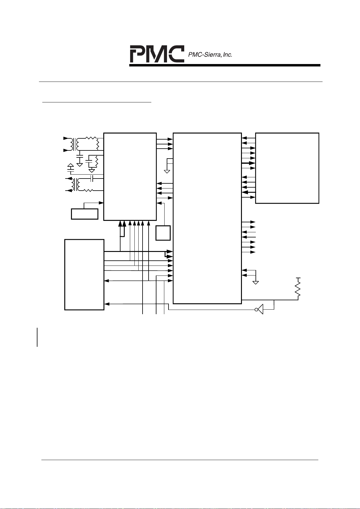
APPLICATION EXAMPLES
Figure 1 - Example 1. T1 or E1 ATM Interface Using PM7345
+5V
AD[7 :0]
ALE
RDB
WRB
RESB
INT
Inte l/
Motorola
Singl e Chip
µP
RAS
REF
RRC
TC
TAP
TAN
BRPCM
BRFPO
RCLKO
BTPCM
BTFP
BTCLK
TCL KO
TCL K I
PM 4341 A
T1XC T1
Transceiver
PM7345
S/UNI-PDH
SATURN
User-Netw ork
Interface for
PDH
RPOS/RDAT
RNEG/ROHM
RCLK
TIOHM
C13/CADD
TPOS/TDAT
TNEG/TOHM
TCLK
TICLK
From Master
rese t c ircu itry
From chip select
decode circuitry
37.056 MHz
RX
CELL
INTERFA C E
TX
CELL
INTERFA C E
ATM/SMD S
Adaptation
Layer
Processor
(SA R o r
po licin g
fun c tio n s )
RRDENB
FRDB/RFCLK
RSOC
REOH
REOC
FRDATA[7:0]
RFIFOE/RCA
TW REN B
FW RB /TFCLK
TSO C
FW DA TA[7:0]
TFIFO FB/TC A
TPOHC L K
TPO H F P
TPO HINS
TPO H
RPOHCLK
RPOHFP
RPOH
TOHINS
TOH
INTB
A[7:0]
D[7:0]
ALE
RDB
WRB
CSB
RSTB
XCLK
1.544
MHz
A[8:0
]
D[7:0]
ALE
RDB
WRB
CSB
RS
TB
Example 1 shows the PM4341 T1XC or PM6341 E1XC used with a PM7345
Saturn User Network Interface for PDH (S/UNI-PDH™) to implement ATM wide
area user network interfaces (UNI) and network node interfaces (NNI).
In this example, the T1 LIU and framing functions are provided by the PM4341A
T1XC. The combination of the T1XC or E1XC devices with the S/UNI-PDH
™
allows both PLCP formatted DS1/E1 signals and CCITT G.804 compliant
DS1/E1 signals to be processed. The G.804 specification defines ATM cell
mappings for a variety of transmission formats, including the 1.544 Mbit/s DS1
and the 2.048 Mbit/s E1 formats.
Page 25
PM4341A T1XC
DATA SHEET
PMC-900602 ISSUE 7 T1 FRAMER/TRANSCEIVER
PROPRIETARY AND CONFIDENTIAL TO PMC-SIERRA, INC., AND FOR ITS CUSTOMERS’ INTERNAL USE
7
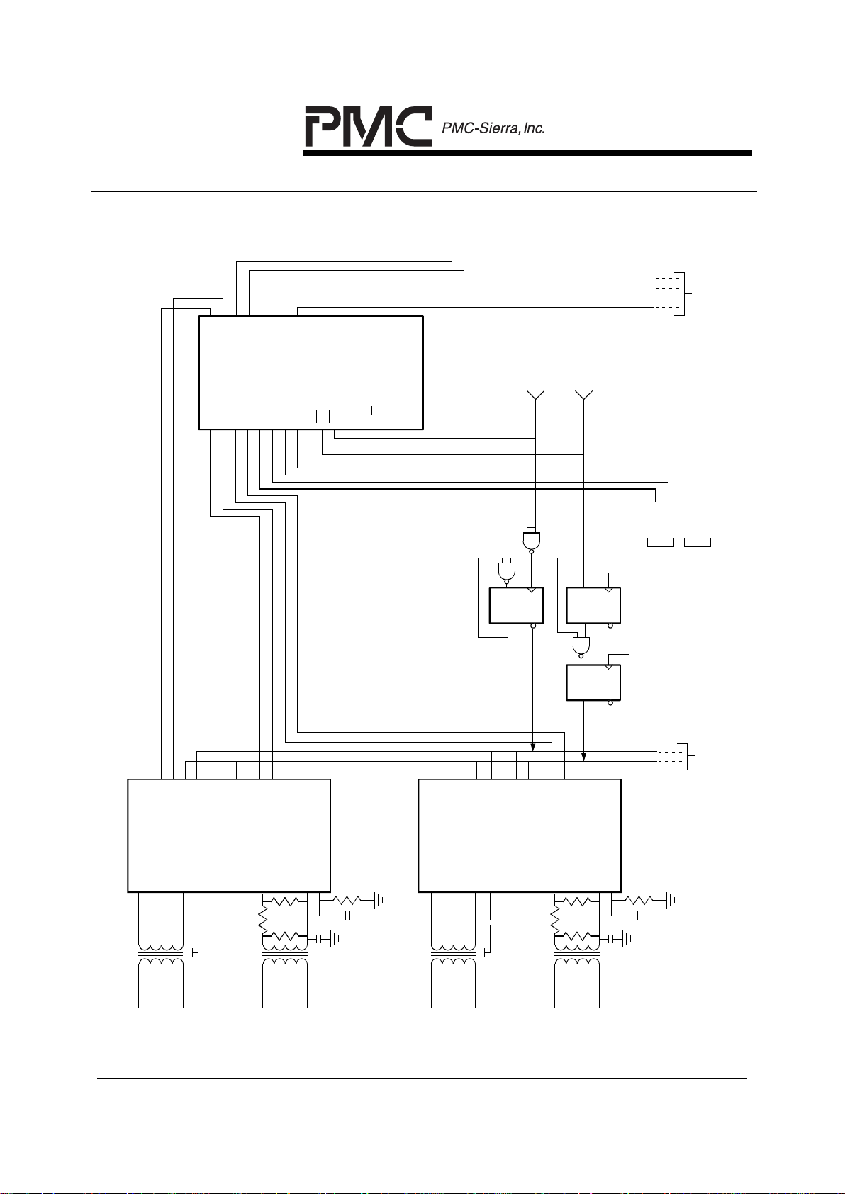
Figure 2 - Example 2. DSX-1/0 Cross-connect
MT8980 DX
PM4341A T1XC
AVS
AVS
4.
0
96
M
H
z
D
AVD
+
to
tr
an
sc
ei
ve
rs
#
3
& 4
to
tr
an
sc
ei
ve
rs
#
3
& 4
#1
fro
m
tr
an
sc
ei
ve
r
#3
fro
m
tr
an
sc
ei
ve
r
#4
PM4341A T1XC
#2
AVS
AVS
AVD
+
D
D
Glu
e
log
ic
ca
n
be
im
pl
eme
nt
ed
us
in
g o
ne
74HCT00 and
one 74HCT
175 pack.
2.048MHz
DSX-1
Tr
an
sm
it
STi
0
STi
1
STi
2
STi
3
STi
4
STi
5
STi
6
STi7F0i
C4i
STo0
STo1
STo2
STo3
STo4
STo5
STo6
STo7
CSTo
ODE
CS
DS
R/W
DTA
A[5:0
]
D[7:0
]
BTPCM
BTS
IG
BTFP
BTCLK
BRCLK
BRFP
I
BRPCM
BRS
IG
BRFPO
TAP
TAN
TC
RAS
REF
RRC
DSX-1
Re
c
e
iv
e
Q
QB
BRPCM
BRS
IG
BRPCM
BRS
IG
BTPCM
BTS
IG
BTFP
BTCLK
BRCLK
BRFP
I
BRPCM
BRS
IG
BRFPO
TAP
TAN
TC
RAS
REF
RRC
DSX-1
Tr
an
sm
it
D
S
X
-1
R
eceive
Sys
te
m
Fr
am
e
Pu
ls
e
Q
QB
Q
QB
Page 26
PM4341A T1XC
DATA SHEET
PMC-900602 ISSUE 7 T1 FRAMER/TRANSCEIVER
PROPRIETARY AND CONFIDENTIAL TO PMC-SIERRA, INC., AND FOR ITS CUSTOMERS’ INTERNAL USE
8
Example 2 shows a DSX 1/0 Cross-Connect utilizing four T1XC chips and a Mitel
MT8980 Digital Time/Space Switch to implement a simple 1/0 cross-connect. An
alternate architecture could use two MT8980s, one as a voice switch and the
other as a signalling switch, and 8 T1XCs to cross-connect eight T1s. (Note: a
true implementation would require redundancy in the switch core.)
In this example, the T1XC chips are programmed to receive and generate the
same framing format, using the 2.048 MHz backplane data rate. The "system
frame pulse" signal is stretched through the two D-FF into a pulse of 488ns
duration, which is used to frame align the data out of each transceiver through
the elastic store and to provide frame alignment indication to the transmitters.
The raw system frame pulse signal is used to indicate frame alignment
synchronization to the MT8980. Another D-FF is configured as a toggle to
generate a 2.048MHz clock from the system 4.096MHz clock source,
synchronized to the system frame pulse.
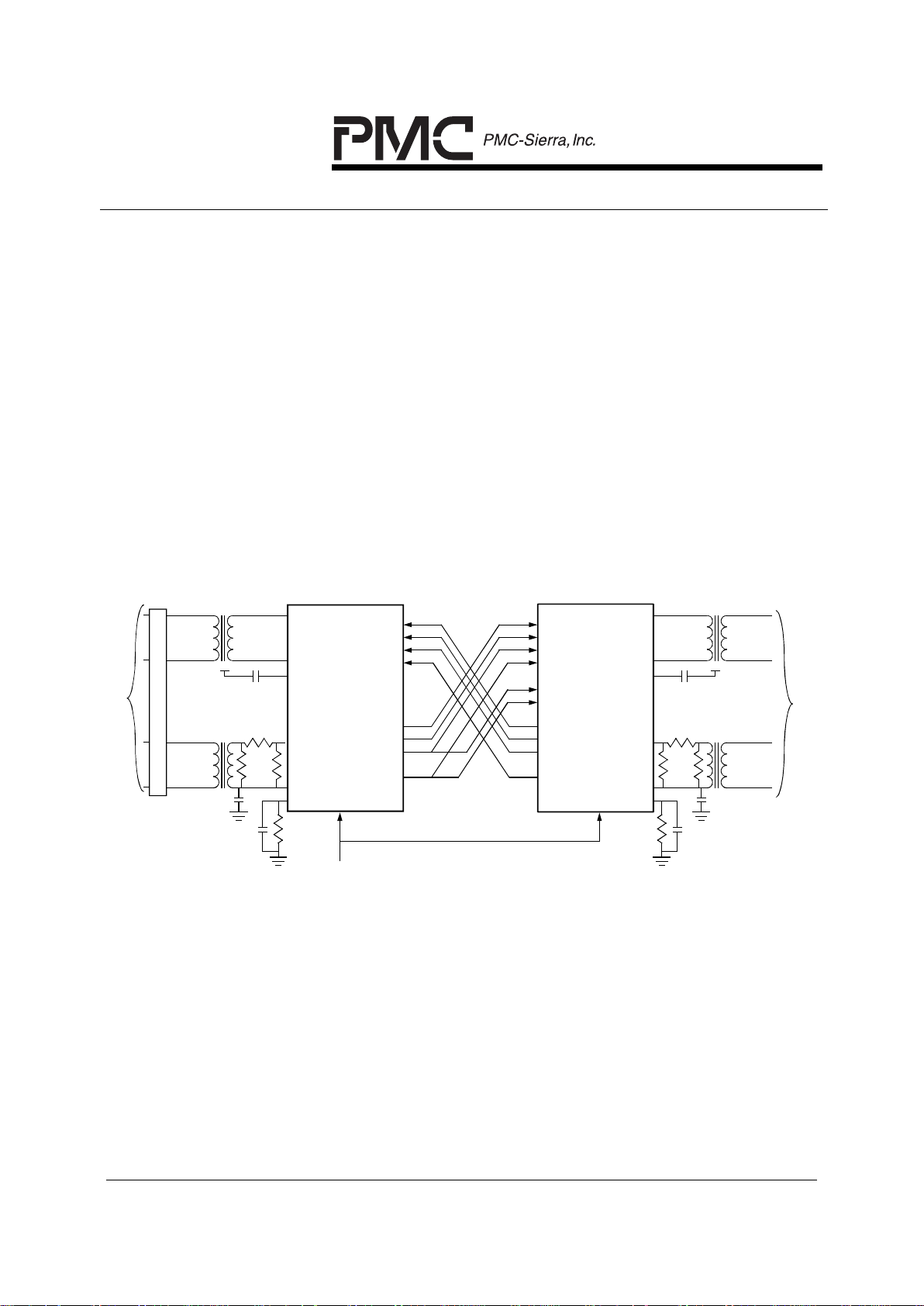
Figure 3 - Example 3. Multi-featured, jitter attenuating CSU
DSX-1
Transmit
PM4
34
1A
T
1XC
BTPCM
BTSIG
BTFP
BTCLK
BRFPI
BRCLK
BRPCM
BRSIG
BRFPO
RCLKO
TAP
TAN
RAS
REF
RRC
DSX-1
Receive
AVS
AVS
AVD
+
#1
DSX-1
Transmit
PM4
34
1A
T
1XC
BTPCM
BTSIG
BTFP
BTCLK
BRFPI
BRCLK
BRPCM
BRSIG
BRFPO
RCLKO
TAP
TAN
RAS
REF
RRC
DSX-1
Receive
AVS
AVS
AVD
+
#2
N
e
t
w
o
r
k
C
u
s
t
o
m
e
r
XCLKXCLK
37.056MHz
Networ
k inte
rface
unit
TC
TC
Example 3 is an application utilizing 2 T1XC chips to implement a multi-featured
Channel Service Unit with jitter attenuation. The T1XCs are programmed to
receive and generate the same framing format, using the 1.544 MHz backplane
data rate with the Elastic Stores bypassed.
T1XC #1's Timing Options Register is programmed to enable jitter attenuation of
the outgoing transmit data to the network, using the backplane transmit clock
(BTCLK= recovered clock from customer interface) as the jitter reference.
Similarly, T1XC #2 is programmed to attenuate the outgoing transmit data jitter to
the customer equipment using its backplane transmit clock (BTCLK= recovered
Page 27

PM4341A T1XC
DATA SHEET
PMC-900602 ISSUE 7 T1 FRAMER/TRANSCEIVER
PROPRIETARY AND CONFIDENTIAL TO PMC-SIERRA, INC., AND FOR ITS CUSTOMERS’ INTERNAL USE
9
clock from network interface) as the jitter reference. Also, since T1XC #2's elastic
store is bypassed, the TRSLIP bit in the Receive Options register can be set to
provide a measure of the frequency difference between the network clock and
the customer clock by monitoring the time interval between resulting slip
indications.
This application can be readily modified to provide additional features by simply
changing the T1XC configurations via software. No external wiring changes are
necessary to support framing format conversion or to loop time the network
transmit data to the network receive recovered clock.
For example, to provide format conversion of a customer's SF-based equipment
to an ESF network, T1XC #1 would be programmed to receive and transmit ESF
formatted data, while providing superframe alignment indication on the
backplane frame pulse output (BRFPO). T1XC #2 would be programmed to
receive and transmit SF formatted data, while providing every second
superframe alignment indication on its BRFPO. To provide loop timing of the
network transmit to the network receive clock, T1XC #2 would be programmed to
use the elastic store, thereby providing the slip buffering to handle the frequency
difference between the network and customer equipment clocks. T1XC #1 would
be programmed to use its RCLKO for the transmitter clock instead of the input
BTCLK.
Page 28
PM4341A T1XC
DATA SHEET
PMC-900602 ISSUE 7 T1 FRAMER/TRANSCEIVER
PROPRIETARY AND CONFIDENTIAL TO PMC-SIERRA, INC., AND FOR ITS CUSTOMERS’ INTERNAL USE
10
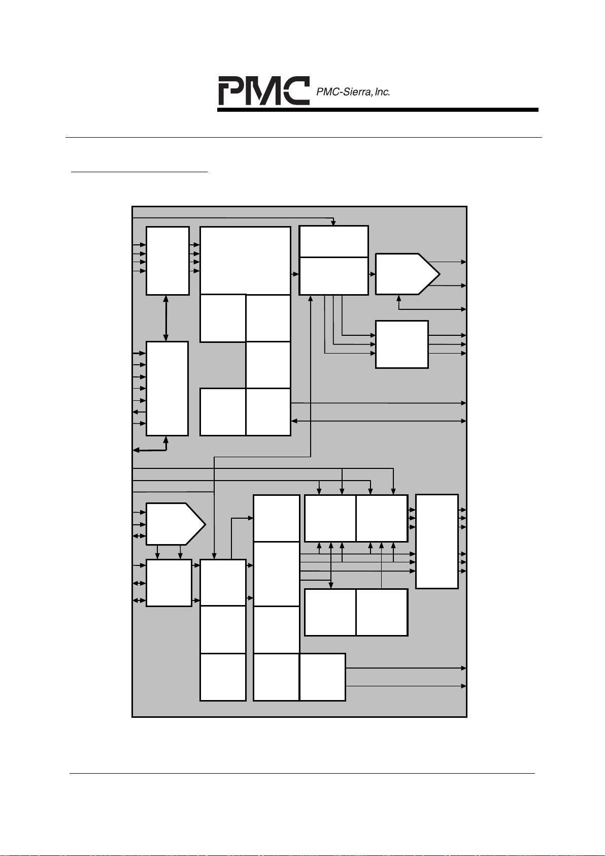
4
BLOCK DIAGRAM
CDRC
CLOCK AND
DATA
RECOVERY
PMON
PER-
FORMANCE
MONITOR
COUNTERS
ALMI
ALARM
INTE-
GRATOR
BRIF
BACK-
PLANE
RECEIVE
INTER-
FACE
BRPCM/BRDP
BRSIG/BRDN
BRFPO
RCLKO
RFP
RDPCM/RPCM
RDLCLK/
RDLEOM
RDLSIG/
RDLINT
TDP/TDD
TCLKO
TDN/TFLG
TAN
TAP
TDLSIG/
TDLINT
TDLCLK/
TDLUDR
TC
TOPS
TIMING
OPTIONS
DJAT
DIGITAL
JITTER
ATTENUATOR
XIBC
IN-BAND
LOOPBACK
CODE
GENERATOR
XBAS
BASICTRANSMITTER:
FRAME GENERATION,
ALARM INSERTION,
TRUNK CONDITIONING
LINE CODING
TPSC
PER-CHAN
CONT:
SIG,IDLE,
ZERO CO NT
DTIF
DIGITAL DS-1
TRANSMIT
INTERFACE
XPLS
ANALOG
DSX-1 PULSE
GENERATOR
XCLK/VCLK
BRFPI
BRCLK
RCLKI
RDP/RDD/
SDP
RDN/RLCV/
SDN/
RAS
REF
RRC
TCLKI
BTPCM/BTDP
BTCLK
BTSIG/BTDN
BTFP
INTB
D(7-0)
A(7-0)
RDB
WRB
CSB
ALE
RSTB
MPIF
MICRO-
PROCESS-
OR
INTERFACE
RECEIVER
TRANSMITTER
XPDE
PULSE
DENSITY
ENFORCER
XFDL
HDLC
TRANSMITTER
XBOC
BIT-
ORIENTED
CODE GEN.
PDVD
PULSE
DENSITY
VIOLATION
DETECTOR
RFDL
HDLC
RECEIVER
RBOC
BIT-
ORIENTED
CODE
DETECTOR
IBCD
IN-BAND
LOOPBACK
CODE
DETECTOR
FRAM
FRAMER/
SLIP BUFFER
RAM
RPSC
PER-CHANNEL
CONTROL:
TRUNK
CONDITION
DRIF
DIGITAL
DS-1 RX
INTER-
FACE
FRMR
FRAMER:
FRAME
ALIGNMENT,
ALARM
EXTRACT
RSLC
ANALOG
DSX-1 PULSE
SLICER
ELST
ELASTIC
STORE
SIGX
SIGNALLING
EXTRACT-
OR
BTIF
BACK-
PLANE
TRANSMIT
INTER-
FACE
TOPS
TIMING
OPTIONS
Page 29

PM4341A T1XC
DATA SHEET
PMC-900602 ISSUE 7 T1 FRAMER/TRANSCEIVER
PROPRIETARY AND CONFIDENTIAL TO PMC-SIERRA, INC., AND FOR ITS CUSTOMERS’ INTERNAL USE
11
5
DESCRIPTION
The PM4341A Single T1 Framer/Transceiver (T1XC) is a feature-rich device
suitable for use in many T1 systems with a minimum of external circuitry. The
T1XC is software configurable, allowing feature selection without changes to
external wiring.
On the receive side, the T1XC recovers clock and data and can be configured to
frame to any of the common DS-1 signal formats: SF, ESF, T1DM (DDS), or
SLC®96. Analog circuitry is provided to allow direct reception of a DSX-1
compatible signal up to 655 feet from the cross-connect by using only an external
transformer and passive components. The T1XC also supports detection of
various alarm conditions such as loss of signal, pulse density violation, red
alarm, yellow alarm, and AIS alarm. The T1XC detects and indicates the
presence of yellow and AIS patterns and also integrates yellow, red, and AIS
alarms as per industry specifications.
Performance monitoring with accumulation of CRC-6 errors, framing bit errors,
line code violations, and loss of frame events is provided. The T1XC also detects
the presence of in-band loopback codes, ESF bit oriented codes, and detects
and terminates HDLC messages on the ESF data link. An elastic store for slip
buffering and adaptation to backplane timing is provided, as is a signalling
extractor that supports signalling debounce, signalling freezing, idle code
substitution, digital milliwatt tone substitution, data inversion, and signalling bit
fixing on a per-channel basis. Receive side data and signalling trunk
conditioning is also provided.
On the transmit side, the T1XC generates framing for SF, ESF, T1DM (DDS), and
SLC®96 DS1 formats, or framing can be optionally disabled. Internal analog
circuitry allows direct transmission of a DSX-1 compatible signal using only an
external transformer. Digitally programmable line build out allows transmission of
DSX-1 compatible signals up to 655 feet from the cross-connect. The T1XC also
supports signalling insertion, idle code substitution, digital milliwatt tone
substitution, data inversion, and zero code suppression on a per-channel basis.
The zero code suppression is selectable to Bell (bit 7), GTE, or DDS standards,
and can also be disabled. Transmit side data and signalling trunk conditioning is
provided.
The T1XC can also generate in-band loopback codes, ESF bit oriented codes,
and transmit HDLC messages on the ESF data link. The T1XC can generate a
low jitter transmit clock and provides a FIFO for transmit jitter attenuation. When
not used for jitter attenuation, the full or empty status of this FIFO is made
Page 30

PM4341A T1XC
DATA SHEET
PMC-900602 ISSUE 7 T1 FRAMER/TRANSCEIVER
PROPRIETARY AND CONFIDENTIAL TO PMC-SIERRA, INC., AND FOR ITS CUSTOMERS’ INTERNAL USE
12
available to facilitate higher order multiplexing applications by controlling bitstuffing logic.
The T1XC provides both a parallel microprocessor interface for controlling the
operation of the T1XC device, and serial PCM interfaces that allow 1.544 Mbit/s
or 2.048 Mbit/s backplanes to be directly supported. Tolerance of gapped clocks
allows other backplane rates to be supported with a minimum of external logic.
Page 31

PM4341A T1XC
DATA SHEET
PMC-900602 ISSUE 7 T1 FRAMER/TRANSCEIVER
PROPRIETARY AND CONFIDENTIAL TO PMC-SIERRA, INC., AND FOR ITS CUSTOMERS’ INTERNAL USE
13
6
PIN DIAGRAM
Figure 4 - 68 Pin PLCC
PM4341A
9 8 7 6 5 4 3 2 1 6867 66656463 6261
XCLK/VCLK
BTPCM/BTDP
BTSIG/BTDN
BTFP
BTCLK
TCLKI
TCLKO
TDP/TDD
VSSO[0]
VDDO[0]
TDN/TFLG
TDLCLK/TDLUDR
TDLSIG/TDLINT
TAVS
TAVD
TAN
VDDO[3]
27 28 29 30 31 32 33 34 35 36 37 38 39 40 41 42 43
A[0]
A[1]
A[2]
A[3]
A[4]
A[5]
A[6]
A[7]
ALE
BRFPI
BRCLK
RFP
RDLCLK/RDLEOM
RDLSIG/RDLINT
RCLKO
RDPCM/RPCM
VSSO[2]
10
11
12
13
14
15
16
17
18
19
20
21
22
23
24
25
26
CSB
RSTB
INTB
D[0]
D[1]
D[2]
D[3]
VSSO[1]
VSSI[0]
VDDI[0]
VDDO[1]
D[4]
D[5]
D[6]
D[7]
RDB
WRB
60
59
58
57
56
55
54
53
52
51
50
49
48
47
46
45
44
VSSO[3]
TC
TAP
RAVD
RAVS
RAS
RRC
REF
VSSI[1]
VDDI[1]
RCLKI
BRFPO
BRPCM/BRDP
BRSIG/BRDN
RDP/RDD/SDP
RDN/RLCV/SDN
VDDO[2]
(TOP VIEW)
Page 32

PM4341A T1XC
DATA SHEET
PMC-900602 ISSUE 7 T1 FRAMER/TRANSCEIVER
PROPRIETARY AND CONFIDENTIAL TO PMC-SIERRA, INC., AND FOR ITS CUSTOMERS’ INTERNAL USE
14
Figure 5 - 80 Pin PQFP
(TOP VIEW)
PM4341A
60
59
58
57
56
55
54
53
52
51
50
49
48
47
46
45
44
43
42
41
1
2
3
4
5
6
7
8
9
10
11
12
13
14
15
16
17
18
19
20
NC
CSB
RSTB
INTB
D[0]
D[1]
D[2]
D[3]
VSSO[1]
VSSI[0]
VDDI[0]
VDDO[1]
D[4]
D[5]
D[6]
D[7]
RDB
WRB
NC
NC
NC
NC
VSSO[3]
TC
TAP
RAVD
RAVS
RAS
RRC
REF
VSSI[1]
VDDI[1]
RCLKI
BRFPO
BRPCM/BRDP
BRSIG/BRDN
RDP/RDD/SDP
RDN/RLCV/SDN
VDDO[2]
NC
22232425262728293031323334353637383940
21
A[0]
A[1]
A[2]
A[3]
A[4]
A[5]
A[6]
A[7]
ALE
BRFPI
BRCLK
RFP
RDLCLK/RDLEOM
RDLSIG/RDLINT
RCLKO
RDPCM/RPCM
VSSO[2]
NC
NC
NC
79787776757473727170696867666564636261
80
NC
XCLK/VCLK
BTPCM/BTDP
BTSIG/BTDN
BTFP
BTCLK
TCLKI
TCLKO
TDP/TDD
VSSO[0]
VDDO[0]
TDN/TFLG
TDLCLK/TDLUD
R
TDLSIG/TDLINT
TAVS
TAVD
TANNCVDDO[3]
NC
Page 33

PM4341A T1XC
DATA SHEET
PMC-900602 ISSUE 7 T1 FRAMER/TRANSCEIVER
PROPRIETARY AND CONFIDENTIAL TO PMC-SIERRA, INC., AND FOR ITS CUSTOMERS’ INTERNAL USE
15
7
PIN DESCRIPTION
Pin Pin No.
Name Type PQFP PLCC Function
RDP/ I/O 44 46 Receive Digital Positive Line Pulse
(RDP). This input is available when the
T1XC is configured to receive dual-rail
formatted data. The RDP input can be
enabled for either RZ or NRZ waveforms.
When enabled for NRZ, this input may
be enabled to be sampled on the rising
or falling edge of RCLKI. When enabled
for RZ, clock is recovered from the RDP
and RDN inputs.
RDD/ Receive Digital DS-1 Signal (RDD).
When the T1XC is configured to receive
single-rail data, this input may be enabled
to be sampled on the rising or falling
edge of RCLKI.
SDP Sliced Positive Line Pulse (SDP). This
pin becomes an output when the receive
analog line interface is powered up. A
positive pulse on the SDP output
corresponds to the sampled positive
pulse excursion on the RAS input.
RDN/ I/O 43 45 Receive Digital Negative Line Pulse
(RDN). This input is available when the
T1XC is configured to receive dual-rail
formatted data. The RDN input can be
enabled for either RZ or NRZ waveforms.
When enabled for NRZ, this input may
be enabled to be sampled on the rising
or falling edge of RCLKI. When enabled
for RZ, clock is recovered from the RDP
and RDN inputs.
Page 34

PM4341A T1XC
DATA SHEET
PMC-900602 ISSUE 7 T1 FRAMER/TRANSCEIVER
PROPRIETARY AND CONFIDENTIAL TO PMC-SIERRA, INC., AND FOR ITS CUSTOMERS’ INTERNAL USE
16
Pin Pin No.
Name Type PQFP PLCC Function
RLCV/ I/O 43 45 Receive Line Code Violation Indication
(RLCV). When the T1XC is configured to
receive single-rail data, this input may be
enabled to be sampled on the rising or
falling edge of RCLKI.
SDN Sliced Negative Line Pulse (SDN). This
pin becomes an output when the receive
analog line interface is powered up. A
positive pulse on the SDN output
corresponds to the sampled negative
pulse excursion on the RAS input.
RCLKI Input 48 50 Receive Line Clock Input (RCLKI). This
input is an externally recovered 1.544
MHz line clock that may be enabled to
sample the RDP and RDN inputs on its
rising or falling edge when the input
format is enabled for dual-rail NRZ; or to
sample the RDD and RLCV inputs on its
rising or falling edge when the input
format is enabled for single-rail.
RAS Input 53 55 Receive Analog Signal (RAS). This
analog input samples the AC signal on
an external isolation transformer. It is
connected to the positive lead of the
transformer secondary through a passive
attenuation network.
REF I/O 51 53 Receive Reference (REF). This analog
bidirectional pin provides DC bias to an
external isolation transformer. It is
connected to the negative lead of the
transformer secondary and to a
decoupling capacitor to RAVS.
Page 35

PM4341A T1XC
DATA SHEET
PMC-900602 ISSUE 7 T1 FRAMER/TRANSCEIVER
PROPRIETARY AND CONFIDENTIAL TO PMC-SIERRA, INC., AND FOR ITS CUSTOMERS’ INTERNAL USE
17
Pin Pin No.
Name Type PQFP PLCC Function
RRC I/O 52 54 Receive Peak Hold R-C Network (RRC).
This analog bidirectional pin is connected
to an external parallel resistor/capacitor
network to RAVS. This network is
necessary to the operation of the internal
peak detector that tracks the incoming
signal level.
RAVD Power 55 57 Receive Analog Power (RAVD). This pin
provides the +5V supply to the receive
analog line interface. If the receive
analog line interface is not used, the
power consumption of the T1XC can be
reduced by connecting the RAVD pin to
the analog ground pin, RAVS. RAVD
must be connected to a common, well
decoupled +5 VDC supply together with
the VDDO[2:0] and VDDI[1:0] pins. Care
must be taken to avoid coupling noise
induced on the VDDO and VDDI pins into
the RAVD pin.
RAVS Ground 54 56 Receive Analog Ground (RAVS). This pin
provides the ground supply to the receive
analog line interface. RAVS must be
connected to a common ground together
with the VSSO[2:0] and VSSI[1:0] pins.
Care must be taken to avoid coupling
noise induced on the VSSO and VSSI
pins into the RAVS pin.
RCLKO Output 36 41 Recovered PCM Clock Output (RCLKO).
This output signal is the recovered 1.544
MHz clock, synchronized to the XCLK
signal. The RCLKO signal is recovered
from the received analog inputs (if the
interface is powered up), from the RDP
and RDN inputs (if the input format is
dual-rail RZ), or from the RCLKI input (if
the input format is NRZ).
Page 36

PM4341A T1XC
DATA SHEET
PMC-900602 ISSUE 7 T1 FRAMER/TRANSCEIVER
PROPRIETARY AND CONFIDENTIAL TO PMC-SIERRA, INC., AND FOR ITS CUSTOMERS’ INTERNAL USE
18
Pin Pin No.
Name Type PQFP PLCC Function
RDPCM/ Output 37 42 Recovered Decoded PCM (RDPCM).
This output is available when the T1XC is
configured for decoded data output. This
NRZ output signal is the recovered data
stream with B8ZS decoding applied, if
B8ZS decoding is enabled. It is updated
on the falling edge of RCLKO. The
RDPCM signal is not meant to be used
when the digital receive interface is
configured for uni-polar operation since
this data should be available at the RDD
input.
RPCM Recovered PCM (RPCM). This output is
available when the T1XC is configured for
raw data output. This NRZ output signal
is the recovered data stream without
optional B8ZS decoding applied. It is
updated on the falling edge of RCLKO.
Page 37

PM4341A T1XC
DATA SHEET
PMC-900602 ISSUE 7 T1 FRAMER/TRANSCEIVER
PROPRIETARY AND CONFIDENTIAL TO PMC-SIERRA, INC., AND FOR ITS CUSTOMERS’ INTERNAL USE
19
Pin Pin No.
Name Type PQFP PLCC Function
RFP Output 33 38 Receive Frame Pulse (RFP). When the
T1XC is configured for receive frame
pulse output, RFP pulses high for 1
RCLKO cycle during bit 1 of each 193-bit
frame, indicating the frame alignment of
the RPCM/RDPCM data stream. RFP
does not indicate the frame alignment in
RDPCM when the digital receive
interface is configured for unipolar
operation (i.e. RUNI=1and RDIEN=1 in
Register 03h).
When configured for receive superframe
output, RFP pulses high for 1 RCLKO
cycle during bit 1 of frame 1 of the 12 or
24 frame superframe, indicating the
superframe alignment of the
RPCM/RDPCM data stream.
When configured for receive alternate
superframe output, RFP pulses high for 1
RCLKO cycle during bit 1 of frame 1 of
every second 12 or 24 frame superframe,
indicating the superframe alignment of
the RPCM/RDPCM data stream. This
alternate superframe indication is useful
for performing format conversion from SF
to ESF while maintaining the same
superframe alignment.
RFP is updated on the falling edge of
RCLKO.
Page 38

PM4341A T1XC
DATA SHEET
PMC-900602 ISSUE 7 T1 FRAMER/TRANSCEIVER
PROPRIETARY AND CONFIDENTIAL TO PMC-SIERRA, INC., AND FOR ITS CUSTOMERS’ INTERNAL USE
20
Pin Pin No.
Name Type PQFP PLCC Function
RDLSIG/ Output 35 40 Receive Data Link Signal (RDLSIG). The
RDLSIG signal is available on this output
when the internal HDLC receiver (RFDL)
is disabled from use, or, optionally, when
the D-channel of the Primary Rate
interface is extracted. When the T1XC is
configured to receive ESF formatted
data, the RDLSIG contains the data
stream extracted from the facility data
link; when the T1XC is configured to
receive SF formatted data, the RDLSIG
output is held low; when the T1XC is
configured to receive T1DM, RDLSIG
reflects the value of the R-bit in the T1DM
sync word; when the T1XC is configured
for SLC®96, RDLSIG contains the value
of the Fs framing bits. When the Dchannel is enabled for extraction,
RDLSIG contains the contents of channel
24 of each DS-1 frame. RDLSIG is
updated on the falling edge of RDLCLK.
RDLINT Receive Data Link Interrupt (RDLINT).
The RDLINT signal is available on this
output when RFDL is enabled. RDLINT
goes high when an event occurs which
changes the status of the HDLC receiver.
Page 39

PM4341A T1XC
DATA SHEET
PMC-900602 ISSUE 7 T1 FRAMER/TRANSCEIVER
PROPRIETARY AND CONFIDENTIAL TO PMC-SIERRA, INC., AND FOR ITS CUSTOMERS’ INTERNAL USE
21
Pin Pin No.
Name Type PQFP PLCC Function
RDLCLK/ Output 34 3 9 Re ceive Data Link Clock (RDLCLK). The
RDLCLK signal is available on this output
when the internal HDLC receiver (RFDL)
is disabled from use, or, optionally, when
the D-channel of the Primary Rate
interface is extracted. RDLCLK is used
to process the data stream contained on
the RDLSIG output. When the T1XC is
configured to receive SF formatted data,
the RDLCLK output is held low. In all
other formats the rising edge of RDLCLK
can be used to sample the data on
RDLSIG.
RDLEOM Receive Data Link End of Message
(RDLEOM). The RDLEOM signal is
available on this output when RFDL is
enabled. RDLEOM goes high when the
last byte of a received sequence is read
from the RFDL FIFO buffer, or when the
FIFO buffer is overrun.
BRPCM/ Output 46 48 Backplane Receive PCM (BRPCM). The
BRPCM signal is available on this output
when the backplane is configured for
single-rail output. BRPCM contains the
recovered data stream passed through
ELST, SIGX, and the RPSC. When the
ELST is not by-passed, the BRPCM
stream is aligned to the backplane timing
and is updated on the falling edge of
BRCLK. When the ELST is by-passed,
BRPCM is aligned to the receive line
timing and is updated on the falling edge
of RCLKO.
Page 40

PM4341A T1XC
DATA SHEET
PMC-900602 ISSUE 7 T1 FRAMER/TRANSCEIVER
PROPRIETARY AND CONFIDENTIAL TO PMC-SIERRA, INC., AND FOR ITS CUSTOMERS’ INTERNAL USE
22
Pin Pin No.
Name Type PQFP PLCC Function
BRDP Output 46 48 Backplane Receive Positive Line Pulse
(BRDP). The BRDP signal is available on
this output when the backplane is
configured for dual-rail output. The
BRDP NRZ output represents the RZ
receive digital positive pulse signal
extracted from the input bipolar signal.
BRDP is updated on the falling edge of
RCLKO.
BRSIG/ Output 45 47 Backplane Receive Signalling (BRSIG).
The BRSIG signal is available on this
output when the backplane is configured
for single-rail output. BRSIG contains the
extracted signalling bits for each channel
in the frame, repeated for the entire
superframe. Each channel's signalling
bits are valid in bit locations 5,6,7,8 of the
channel and are channel-aligned with the
BRPCM data stream. When the ELST is
not by-passed, the BRSIG stream is
aligned to the backplane timing and is
updated on the falling edge of BRCLK.
When the ELST is by-passed, BRSIG is
aligned to the receive line timing and is
updated on the falling edge of RCLKO.
BRDN Backplane Receive Negative Line Pulse
(BRDN). The BRDN signal is available
on this output when the backplane is
configured for dual-rail output. The
BRDN NRZ output represents th e RZ
receive digital negative pulse signal
extracted from the input bipolar signal.
BRDN is updated on the falling edge of
RCLKO.
Page 41

PM4341A T1XC
DATA SHEET
PMC-900602 ISSUE 7 T1 FRAMER/TRANSCEIVER
PROPRIETARY AND CONFIDENTIAL TO PMC-SIERRA, INC., AND FOR ITS CUSTOMERS’ INTERNAL USE
23
Pin Pin No.
Name Type PQFP PLCC Function
BRFPO Output 47 49 Backplane Frame Pulse Output
(BRFPO). When the T1XC is configured
for backplane receive frame pulse output,
BRFPO pulses high for 1 BRCLK cycle
(or 1 RCLKO cycle if ELST is by-passed)
during bit 1 of each 193-bit frame,
indicating the frame alignment of the
BRPCM data stream.
When configured for backplane receive
superframe output, BRFPO pulses high
for 1 BRCLK cycle (or 1 RCLKO cycle if
ELST is by-passed) during bit 1 of frame
1 of the 12 or 24 frame superframe,
indicating the superframe alignment of
the BRPCM data stream.
When configured for backplane alternate
receive superframe output, BRFPO
pulses high for 1 BRCLK cycle (or 1
RCLKO cycle if ELST is by-passed)
during bit 1 of frame 1 of every second
12 or 24 frame superframe, indicating the
superframe alignment of the BRPCM
data stream. This alternate superframe
indication is useful for performing format
conversion from SF to ESF while
maintaining the same superframe
alignment.
BRFPO is updated on the falling edge of
BRCLK or RCLKO.
BRCLK Input 32 37 Backplane Receive Clock (BRCLK). This
clock should be either 1.544MHz or
2.048MHz with optional gapping for
adaptation to non-uniform backplane
data streams. The T1XC may be
configured to ignore the BRCLK input
and use the RCLKO signal in its place
when the ELST is bypassed.
Page 42

PM4341A T1XC
DATA SHEET
PMC-900602 ISSUE 7 T1 FRAMER/TRANSCEIVER
PROPRIETARY AND CONFIDENTIAL TO PMC-SIERRA, INC., AND FOR ITS CUSTOMERS’ INTERNAL USE
24
Pin Pin No.
Name Type PQFP PLCC Function
BRFPI Input 31 36 Backplane Frame Pulse Input (BRFPI).
This input is used to frame align the
received data to the system backplane. If
frame alignment only is required, a pulse
at least 1 BRCLK cycle wide must be
provided on BRFPI every 193 bit times. If
receive signalling alignment is required,
receive signalling alignment must be
enabled, and a pulse at least 1 BRCLK
cycle wide must be provided on BRFPI
every 12 or 24 frame times. BRFPI is
sampled on the rising edge of BRCLK.
BTPCM/ Input 77 8 Backplane Transmit PCM (BTPCM). The
non-return to zero, digital data stream to
be transmitted is input on this pin when
the backplane is configured for single-rail
input. The BTPCM signal is sampled on
the rising edge of BTCLK.
BTDP Backplane Transmit Positive Line Pulse
(BTDP). The positive pulse of the dualrail signal to be transmitted is input on
this pin when the backplane is configured
for dual-rail input. In dual-rail input mode,
the BTDP input by-passes the
transmitter and is fed directly into the
DJAT. BTDP is sampled on the rising
edge of BTCLK.
Page 43

PM4341A T1XC
DATA SHEET
PMC-900602 ISSUE 7 T1 FRAMER/TRANSCEIVER
PROPRIETARY AND CONFIDENTIAL TO PMC-SIERRA, INC., AND FOR ITS CUSTOMERS’ INTERNAL USE
25
Pin Pin No.
Name Type PQFP PLCC Function
BTSIG/ Input 76 7 Backplane Transmit Signalling (BTSIG).
The BTSIG input signal contains the
signalling bits for each channel in the
transmit data frame, repeated for the
entire superframe. This signal is input on
the BTSIG pin when the backplane is
configured for single-rail input. Each
channel's signalling bits are in bit
locations 5,6,7,8 of the channel and are
channel-aligned with the BTPCM data
stream. BTSIG is sampled on the rising
edge of BTCLK.
BTDN Backplane Transmit Negative Line Pulse
(BTDN). The negative pulse of dual-rail
signal to be transmitted is input on this
pin when the backplane is configured for
dual-rail input. In dual-rail input mode,
the BTDN input by-passes the
transmitter and is fed directly into the
DJAT. BTDN is sampled on the rising
edge of BTCLK.
BTFP Input 75 6 Backplane Transmit Frame Pulse (BTFP).
This input is used to frame align the
transmitter to the system backplane. If
frame alignment only is required, a pulse
at least 1 BTCLK cycle wide must be
provided on BTFP every 193 bit times. If
superframe alignment is required,
transmit superframe alignment must be
enabled, and a pulse at least 1 BTCLK
cycle wide must be provided on BTFP
every 12 or 24 frame times.
Page 44

PM4341A T1XC
DATA SHEET
PMC-900602 ISSUE 7 T1 FRAMER/TRANSCEIVER
PROPRIETARY AND CONFIDENTIAL TO PMC-SIERRA, INC., AND FOR ITS CUSTOMERS’ INTERNAL USE
26
Pin Pin No.
Name Type PQFP PLCC Function
BTCLK Input 74 5 Backplane Transmit Clock (BTCLK). This
clock should be either 1.544MHz or
2.048MHz with optional gapping for
adaptation from non-uniform backplane
data streams. The T1XC may be
configured to ignore the BTCLK input
and use the RCLKO signal in its place.
TDLSIG/ I/O 66 65 Transmit Data Link Signal (TDLSIG). The
TDLSIG signal is input on this pin when
the internal HDLC transmitter (XFDL) is
disabled from use. TDLSIG is the source
for the data stream to be inserted into the
ESF data link. When the T1XC is
configured to transmit SLC®96
formatted data, the TDLSIG input is the
source for the Fs framing bits; when the
T1XC is configured to transmit T1DM
with R-bit replacement, TDLSIG is the
source of the R-bit in the T1DM sync
word. TDLSIG is sampled on the rising
edge of TDLCLK.
TDLINT Transmit Data Link Interrupt (TDLINT).
The TDLINT signal is output on this pin
when XFDL is enabled. TDLINT goes
high when the last data byte written to
the XFDL has been set up for
transmission and processor intervention
is required to either write control
information to end the message, or to
provide more data.
Page 45

PM4341A T1XC
DATA SHEET
PMC-900602 ISSUE 7 T1 FRAMER/TRANSCEIVER
PROPRIETARY AND CONFIDENTIAL TO PMC-SIERRA, INC., AND FOR ITS CUSTOMERS’ INTERNAL USE
27
Pin Pin No.
Name Type PQFP PLCC Function
TDLCLK/ Output 67 66 Transmit Data Link Clock (TDLCLK). The
TDLCLK signal is available on this output
when the internal HDLC transmitter
(XFDL) is disabled from use. The rising
edge of TDLCLK is used to sample the
data stream contained on the TDLSIG
input. When the T1XC is configured to
transmit SF formatted data, the TDLCLK
output is held low.
TDLUDR Transmit Data Link Underrun (TDLUDR).
The TDLUDR signal is available on this
output when XFDL is enabled. TDLUDR
goes high when the processor has failed
to service the TDLINT interrupt before
the transmit buffer is emptied.
TCLKO Output 72 3 Transmit Clock Output (TCLKO). The
TDP, TDN, and TDD outputs may be
enabled to be updated on the rising or
falling edge of TCLKO. The TAP and TAN
outputs are also driven with timing
derived from TCLKO. TCLKO is a 1.544
MHz clock that is adequately jitter and
wander free in absolute terms to permit
an acceptable DSX-1 or DS-1 signal to
be generated. Depending on the
configuration of the T1XC, TCLKO may
be derived from TCLKI, RCLKO, or
BTCLK, with or without jitter attenuation.
TDP/ Output 71 2 Transmit Digital Positive Line Pulse
(TDP). This signal is available on the
output when the T1XC is configured to
transmit dual-rail data. The TDP signal
can be formatted for either RZ or NRZ
waveforms, and can be enabled to be
updated on the rising or falling edge of
TCLKO.
Page 46

PM4341A T1XC
DATA SHEET
PMC-900602 ISSUE 7 T1 FRAMER/TRANSCEIVER
PROPRIETARY AND CONFIDENTIAL TO PMC-SIERRA, INC., AND FOR ITS CUSTOMERS’ INTERNAL USE
28
Pin Pin No.
Name Type PQFP PLCC Function
TDD Output 71 2 Transmit Digital DS-1 Signal (TDD). This
signal is available on the output when
configured to transmit single-rail data.
The TDD signal may be enabled to be
updated on the rising or falling edge of
TCLKO.
TDN/ Output 68 67 Transmit Digital Negative Line Pulse
(TDN). This signal is available on the
output when the T1XC is configured to
transmit dual-rail data. The TDN signal
can be formatted for either RZ or NRZ
waveforms, and can be enabled to be
updated on the rising or falling edge of
TCLKO.
TFLG Transmit FIFO Flag (TFLG). This signal
is available when configured to transmit
single-rail data. The TFLG output
indicates when the transmit rate
conversion FIFO in DJAT is nearing an
empty or a full condition. Either
indication may be selected. This output
may be enabled to be updated on the
rising or falling edge of TCLKO.
TAP Output 56 58 Transmit Analog Positive Pulse (TAP).
This analog output drives an AC signal
through an external matching
transformer. It is connected to the
positive lead of the transformer primary.
An analog Transmit Monitor Positive point
is internally bonded to this output and is
used to monitor the positive pulses on
the transmit line.
Page 47

PM4341A T1XC
DATA SHEET
PMC-900602 ISSUE 7 T1 FRAMER/TRANSCEIVER
PROPRIETARY AND CONFIDENTIAL TO PMC-SIERRA, INC., AND FOR ITS CUSTOMERS’ INTERNAL USE
29
Pin Pin No.
Name Type PQFP PLCC Function
TAN Output 63 62 Transmit Analog Negative Pulse (TAN).
This analog output drives an AC signal
through an external matching
transformer. It is connected to the
negative lead of the transformer primary.
An analog Transmit Monitor Negative
point is internally bonded to this output
and is used to monitor the negative
pulses on the transmit line.
TC I/O 57 59 Transmit Reference Decoupling
Capacitor (TC). This analog bidirectional
provides decoupling for an internal
reference generator. It is connected to a
decoupling capacitor to TAVD.
TAVD Power 64 63 Transmit Analog Power (TAVD). This pin
provides the +5 V supply to the transmit
analog line interface. Even if the transmit
analog line interface is not used, a +5 V
supply must be provided. TAVD must be
connected to a common, well decoupled
+5 VDC supply together with the
VDDO[2:0] and VDDI[1:0] pins. Care
must be taken to avoid coupling noise
induced on the VDDO and VDDI pins into
the TAVD pin.
TAVS Ground 65 64 Transmit Analog Ground (TAVS). This pin
provides the ground supply to the
transmit analog line interface. TAVS must
be connected to a common ground
together with the VSSO[2:0] and
VSSI[1:0] pins. Care must be taken to
avoid coupling noise induced on the
VSSO and VSSI pins into the TAVS pin.
Page 48

PM4341A T1XC
DATA SHEET
PMC-900602 ISSUE 7 T1 FRAMER/TRANSCEIVER
PROPRIETARY AND CONFIDENTIAL TO PMC-SIERRA, INC., AND FOR ITS CUSTOMERS’ INTERNAL USE
30
Pin Pin No.
Name Type PQFP PLCC Function
TCLKI Input 73 4 Transmit Clock Input (TCLKI). This input
signal is used to generate the TCLKO
clock signal. Depending upon the
configuration of the T1XC, TCLKO may
be derived directly from TCLKI by dividing
TCLKI by 8, or TCLKO may be derived
from TCLKI after jitter attenuation. If
TCLKI is jitter-free when divided down to
8 kHz, then it is possible to derive TCLKO
from TCLKI when TCLKI is a multiple of 8
kHz (i.e. Nx8 kHz, for N equals 1 to 256).
The T1XC may be configured to ignore
the TCLKI input and utilize BTCLK or
RCLKO instead. RCLKO is also
substituted for TCLKI if line loopback is
enabled.
XCLK/ Input 78 9 Crystal Clock Input (XCLK). This signal
provides timing for many portions of the
T1XC. Depending on the configuration of
the T1XC, XCLK is nominally a 37.056
MHz ± 32ppm or 12.352 MHz ± 50ppm,
50% duty cycle clock.
VCLK When transmit clock generation or jitter
attenuation is not required, XCLK may be
driven with a 12.352 MHz clock. When
transmit clock generation or jitter
attenuation is required, XCLK must be
driven with a 37.056 MHz clock.
Implementation of Line Loopback is also
simplified when a 37.056 MHz clock is
used.
Vector Clock (VCLK). The VCLK signal is
used during T1XC production test to
verify internal functionality.
Page 49

PM4341A T1XC
DATA SHEET
PMC-900602 ISSUE 7 T1 FRAMER/TRANSCEIVER
PROPRIETARY AND CONFIDENTIAL TO PMC-SIERRA, INC., AND FOR ITS CUSTOMERS’ INTERNAL USE
31
Pin Pin No.
Name Type PQFP PLCC Function
INTB Output 4 12 Active low open-drain Interrupt signal
(INTB). This signal goes low when an
unmasked interrupt event is detected on
any of the internal interrupt sources,
including the internal HDLC transceiver.
Note that INTB will remain low until all
active, unmasked interrupt sources are
acknowledged at their source.
CSB Input 2 10 Active low chip select (CSB). This signal
must be low to enable T1XC register
accesses. CSB must go high at least
once after a powerup to clear internal
test modes. If CSB is not used, then it
should be tied to an inverted version of
RSTB, in which case RDB and WRB
determine register access.
D[0]
D[1]
D[2]
D[3]
D[4]
D[5]
D[6]
D[7]
I/O 5
6
7
8
13
14
15
16
13
14
15
16
21
22
23
24
Bidirectional data bus (D[7:0]). This bus is
used during T1XC read and write
accesses.
RDB Input 17 25 Active low read enable (RDB). This signal
is pulsed low to enable a T1XC register
read access. The T1XC drives the D[7:0]
bus with the contents of the addressed
register while RDB and CSB are both
low.
Page 50

PM4341A T1XC
DATA SHEET
PMC-900602 ISSUE 7 T1 FRAMER/TRANSCEIVER
PROPRIETARY AND CONFIDENTIAL TO PMC-SIERRA, INC., AND FOR ITS CUSTOMERS’ INTERNAL USE
32
Pin Pin No.
Name Type PQFP PLCC Function
WRB Input 18 26 Active low write strobe (WRB). This signal
is pulsed low to enable a T1XC register
write access. The D[7:0] bus contents
are clocked into the addressed normal
mode register on the rising edge of WRB
+ CSB, where ‘+’ indicates a logical or.
ALE Input 30 35 Address latch enable (ALE). This signal
latches the address bus contents, A[7:0],
when low, allowing the T1XC to be
interfaced to a multiplexed address/data
bus. When ALE is high, the address
latches are transparent.
RSTB Input 3 1 1 Active low reset (RSTB). This signal is set
low to asynchronously reset the T1XC.
RSTB is a Schmitt-trigger input with
integral pull-up.
A[0]
A[1]
A[2]
A[3]
A[4]
A[5]
A[6]
A[7]
Input 22
23
24
25
26
27
28
29
27
28
29
30
31
32
33
34
Address bus (A[7:0]). This bus selects
specific registers during T1XC register
accesses.
VDDO[0]
VDDO[1]
VDDO[2]
VDDO[3]
Power 69
12
42
62
68
20
44
61
Pad ring power pins (VDDO[3:0]). These
pins must be connected to a common,
well decoupled +5 VDC supply together
with the VDDI[1:0] pins. Care must be
taken to avoid coupling noise induced on
the VDDO pins into the VDDI pins.
Page 51

PM4341A T1XC
DATA SHEET
PMC-900602 ISSUE 7 T1 FRAMER/TRANSCEIVER
PROPRIETARY AND CONFIDENTIAL TO PMC-SIERRA, INC., AND FOR ITS CUSTOMERS’ INTERNAL USE
33
Pin Pin No.
Name Type PQFP PLCC Function
VDDI[0]
VDDI[1]
Power 11
49
19
51
Core power pins (VDDI[1:0]). These pins
must be connected to a common, well
decoupled +5 VDC supply together with
the VDDO[2:0] pins.
VSSO[0]
VSSO[1]
VSSO[2]
VSSO[3]
Ground 70
9
38
58
1
17
43
60
Pad ring ground pins (VSSO[3:0]). These
pins must be connected to a common
ground together with the VSSI[1:0] pins.
Care must be taken to avoid coupling
noise induced on the VSSO pins into the
VSSI pins.
VSSI[0]
VSSI[1]
Ground 10
50
18
52
Core ground pins (VSSI[1:0]). These pins
must be connected to a common ground
together with the VSSO[2:0] pins.
Notes on Pin Description:
1. VDDI and VSSI are the +5 V and ground connections, respectively, for the
core circuitry of the device. VDDO and VSSO are the +5 V and ground
connections, respectively, for the pad ring circuitry of the device. TAVD and
TAVS are the +5V and ground connections, respectively, for the transmit
analog circuitry of the device. These power supply connections must all be
utilized and must all connect to a common +5 V or ground rail, as appropriate.
There is no low impedance connection within the PM4341A between the
core, pad ring, and transmit analog supply rails. Failure to properly make
these connections may result in improper operation or damage to the device.
Care must be taken to avoid coupling of noise into the transmit analog supply
rails.
2. RAVD and RAVS are the +5 V and ground connections, respectively, for the
receive analog circuitry of the device. These power supply connections need
only be used if the receive analog function is desired and should then
connect to a common +5 V or ground rail, as appropriate, with the core, pad
ring, and transmit analog supply rails. There is no low impedance connection
within the PM4341A between the receive analog supply rail and other supply
rails. When the receive analog function is not desired, RAVD should be
connected to RAVS. Care must be taken to avoid coupling of noise into the
receive analog supply rails.
Page 52

PM4341A T1XC
DATA SHEET
PMC-900602 ISSUE 7 T1 FRAMER/TRANSCEIVER
PROPRIETARY AND CONFIDENTIAL TO PMC-SIERRA, INC., AND FOR ITS CUSTOMERS’ INTERNAL USE
34
3. Inputs RSTB and ALE have integral pull-up resistors.
4. Pins 1,19,20,21,39,40,41,59,60,61,79, and 80 on the 80-pin PQFP are not
connected. These pins should be left unconnected in any application.
5. The TDLSIG/TDLINT pin has an integral pull-up resistor and defaults to being
an input after a reset.
6. When the internal RFDL is enabled, the RDLINT output goes high:
• when the number of bytes specified in the RFDL Interrupt
Status/Control Register have been received on the data link,
• immediately on detection of RFDL FIFO buffer overrun,
• immediately on detection of end of message,
• immediately on detection of an abort condition, or,
• immediately on detection of the transition from receiving all ones to
flags.
The interrupt is cleared at the start of the next RFDL Data Register read that
results in an empty FIFO buffer. This is independent of the FIFO buffer fill
level for which the interrupt is p ro grammed. If there is still data remaining in
the buffer, RDLINT will remain high. An interrupt due to a RFDL FIFO buffer
overrun condition is not cleared on a RFDL Data Register read but on a
RFDL Status Register read. The RDLINT output can always be forced low by
disabling the RFDL (setting the EN bit in the RFDL Configuration Register to
logic 0, or by disabling the internal HDLC receiver in the T1XC Receive Data
Link Configuration Register), or by forcing the RFDL to terminate reception
(setting the TR bit in the RFDL Configuration Register to logic 1).
The RDLINT output may be forced low by disabling the interrupts with the
RFDL Interrupt Status/Control Register. However, the internal interrupt latch
is not cleared, and the state of this latch can still be read through the RFDL
Interrupt Status/Control Register.
7. The RDLEOM output goes high:
• immediately on detection of RFDL FIFO buffer overrun,
• when the data byte written into the RFDL FIFO buffer due to an end
of message condition is read,
• when the data byte written into the RFDL FIFO buffer due to an
abort condition is read, or,
Page 53

PM4341A T1XC
DATA SHEET
PMC-900602 ISSUE 7 T1 FRAMER/TRANSCEIVER
PROPRIETARY AND CONFIDENTIAL TO PMC-SIERRA, INC., AND FOR ITS CUSTOMERS’ INTERNAL USE
35
•
when the data byte written into the RFDL FIFO buffer due to the
transition from receiving all ones to flags is read.
RDLEOM is set low by reading the RFDL Status Register or by disabling the
RFDL.
8. The TDLUDR output goes high when the processor is unable to service the
TDLINT request for more data within a specific time-out period. This period is
dependent upon the frequency of TDLCLK:
•
for a TDLCLK frequency of 4 kHz (ESF FDL at the full 4 kHz rate),
the time-out is 1.0 ms;
•
for a TDLCLK frequency of 2 kHz (half the ESF FDL), the time-out
is 2.0ms;
•
for a TDLCLK frequency of 8 kHz (T1DM R-bit insertion), the timeout is 500µs.
Page 54

PM4341A T1XC
DATA SHEET
PMC-900602 ISSUE 7 T1 FRAMER/TRANSCEIVER
PROPRIETARY AND CONFIDENTIAL TO PMC-SIERRA, INC., AND FOR ITS CUSTOMERS’ INTERNAL USE
36
8
FUNCTIONAL DESCRIPTION
8.1 Digital DS-1 Receive Interface (DRIF)
The Digital DS-1 Receive Interface provides control over the various input options
available on the multifunctional digital receive pins RDP/RDD/SDP and
RDN/RLCV/SDN. When configured for dual-rail input, the multifunctional pins
become the RDP and RDN inputs. These inputs can be enabled to receive either
return-to-zero (RZ) or non-return-to-zero (NRZ) signals; the NRZ input signals can
be sampled on either the rising or falling edge of RCLKI. When the interface is
configured for single-rail input, the multifunctional pins become the RDD and RLCV
inputs, which can be sampled on either the rising or falling RCLKI edge. Finally,
when the analog interface is used, the multifunction pins become the SDP and SDN
outputs, indicating the sliced pulses corresponding to the received positive and
negative analog line pulses.
8.2 Analog DSX-1 Pulse Slicer (RSLC)
The Analog DSX-1 Pulse Slicer function is provided by the RSLC block. The
Receive Data Slicer (RSLC) block provides the first stage of signal conditioning
for a G.703 1544kbit/s serial data stream by converting bipolar line signals to
dual rail RZ pulses. Before an RZ output pulse is generated by the RSLC block,
bipolar input signals must rise to 67% of their peak amplitude. This level is
referred to as the slicing level. The threshold criteria insures accurate pulse or
mark recognition in the presence of noise.
The RSLC block can be disabled by strapping the receive analog power pin,
RAVD to ground. When RLSC is disabled, the T1XC accepts RZ DS1 input
pulses on the RDP/RDD and RDN/RLCV pins.
The RSLC block relies on an external network for compliance to the DSX-1 input
port specifications. The RSLC block is configured via an off-chip attenuator pad
to operate in one of two modes: terminating mode or bridging mode.
According to G.703, the amplitude of a DSX-1 terminating mode received pulse
at the 1:2 line-coupling transformer's primary should be in the range from 3.6V to
1.2V (depending on the length of the cable from the signal source). In this mode,
the T1XC can receive signal levels down to a squelching level of 227mV±20%.
Assuming a worst-case squelching level of 272mV, there is 12.9dB margin
between the minimum expected signal level and the minimum receivable signal
level.
Page 55

PM4341A T1XC
DATA SHEET
PMC-900602 ISSUE 7 T1 FRAMER/TRANSCEIVER
PROPRIETARY AND CONFIDENTIAL TO PMC-SIERRA, INC., AND FOR ITS CUSTOMERS’ INTERNAL USE
37
In bridging mode, the T1XC is connected to a monitor jack which bridges across
the line and attenuates the signal levels by 20 dB, so the expected pulse
amplitude at the 1:2 line-coupling transformer's primary should be in the range
from 360mV to 120mV (depending on the length of the cable from the signal
source). In this mode, the T1XC can receive signal levels down to a squelching
level of 50mV±20% which means that there is 6.0dB margin between the
minimum expected signal level and the minimum receivable signal level, in the
worst case.
The RSLC block provides a squelching circuit, which indicates an alarm when
input pulses are below the squelching level threshold. In this state, data is not
sliced, which prevents the detection of noise on an idle transmission line. The
SQ status bit in the RSLC Interrupt Enable/Status register (5DH) goes high
whenever the RSLC block is squelching the input signal. The RSLC can be
configured to generate an interrupt whenever the SQ status bit changes state.
The off-chip attenuator pad network is shown in Figure 6 and the network values
below are recommended for the specified applications:
Table 1 - Recommended Receive Network Values
Mode Turns Ratio
(N ± 5%)
R1 (Ω ± 1%) R2 (Ω ± 1%)
Squelch
Level at
Primary (mV
± 20%)
Terminating 2 309 93 227
Bridging 2 0 402 50
Tight tolerances are required on the resistors and turns ratio to meet the return
loss specification.
Page 56

PM4341A T1XC
DATA SHEET
PMC-900602 ISSUE 7 T1 FRAMER/TRANSCEIVER
PROPRIETARY AND CONFIDENTIAL TO PMC-SIERRA, INC., AND FOR ITS CUSTOMERS’ INTERNAL USE
38
Figure 6 - External Analog Receive Interface Circuit
T
R
1:N
316 kΩ ±1%
47 nF
±10%
RAS
REF
V
RAVS
RAVD
RRC
0.1 µF
± 10%
R2
R1
DD
2. Some transformer manufacturers produce a dual part containing both the 1:2 & 1:1.36
transformers required for the receive and transmit interfaces, respectively.
1. All capacitors ceramic
Notes:
The transformer used should be designed for use in T1 applications. Many
manufacturers have standard products for these applications. Typical
characteristics of a suitable transformer are given in the following table.
Table 2 - Typical Characteristics of Receive Transformer
Turns
Ratio
(PRI:SEC)
OCL (mH
min.)
C
w/w
(pF
max.)
LL (µH
max.)
DCR pri.
(Ω max.)
DCR sec.
(Ω max.)
1:2 1.20 35 0.80 0.80 1.2
where OCL is the open-circuit inductance,
C
w/w
is the inter-winding capacitance,
LLis the leakage inductance, and
DCR is the DC resistance.
Page 57

PM4341A T1XC
DATA SHEET
PMC-900602 ISSUE 7 T1 FRAMER/TRANSCEIVER
PROPRIETARY AND CONFIDENTIAL TO PMC-SIERRA, INC., AND FOR ITS CUSTOMERS’ INTERNAL USE
39
PMC-Sierra has verified the operation of the RSLC functional block with the
following transformers:
• Pulse Engineering PE64931 (1:1:1) and PE64952 (1:2CT)
• BH Electronics 500-1775 (1:1:1) and 500-1777 (1:2CT)
Many manufacturers produce dual transformers containing the 1:2 CT and 1:1.36
transformers necessary for the receiver and transmitter circuits. PMC-Sierra has
verified the operation of XPLS and RSLC with the following dual parts:
• Pulse Engineering PE64952
• Pulse Engineering PE65774 (for extended temperature range)
BH Electronics 500-1777
8.3 Clock and Data Recovery (CDRC)
The Clock and Data Recovery function is provided by a Data and Clock
Recovery (CDRC) block. The CDRC provides clock and PCM data recovery,
B8ZS decoding, line code violation detection, and loss of signal detection. It
recovers the clock from the incoming RZ data pulses using a digital phaselocked-loop and recovers the NRZ data. Loss of signal is indicated after 176
consecutive bit periods of the absence of pulses on both the positive and
negative line pulse inputs and is cleared after the occurrence of a single line
pulse. If enabled, a microprocessor interrupt is generated when a loss of signal
is detected and when the signal returns. A line code violation is defined as a
bipolar violation (BPV) for AMI-coded signals and is defined as a BPV that is not
part of a zero substitution code for B8ZS-coded signals.
The input jitter tolerance of CDRC complies with the Bell Core Document
TA-TSY-000170 and with the AT&T specification TR62411. The tolerance is
measured with a QRSS sequence (220-1 with 14 zero restriction). The CDRC
block provides two algorithms for clock recovery that result in differing jitter
tolerance characteristics. The first algorithm (when the ALGSEL register bit is
logic 0) provides good low frequency jitter tolerance, but the high frequency
tolerance is close to the TR62411 limit. The second algorithm (when ALGSEL is
logic 1) provides much better high frequency jitter tolerance (approaching
0.5UIpp) at the expense of the low frequency tolerance; the low frequency
tolerance of the second algorithm is approximately 80% of that of the first
algorithm.
Page 58

PM4341A T1XC
DATA SHEET
PMC-900602 ISSUE 7 T1 FRAMER/TRANSCEIVER
PROPRIETARY AND CONFIDENTIAL TO PMC-SIERRA, INC., AND FOR ITS CUSTOMERS’ INTERNAL USE
40
Figure 7 - CDRC Jitter Tolerance
10
0.3
0.31
10
100
0.4
AT&T SPEC.
BELLCORE SPEC.
IN SPEC. REGION
CDRC MAX. TOLERANCE
(ALGSEL=0)
SINEWAVE JITTER FREQUENCY, kHz - LOG SCALE
SINEWAVE
JITTER
AMPLITUDE
P. TO P. (UI)
LOG SCALE
CDRC MAX. TOLERANCE
(ALGSEL=1)
0.70
8.4 Framer (FRMR)
The framing function is provided by the FRMR block. This block searches for the
framing bit position in the incoming recovered PCM stream. It works in
conjunction with the FRAM block and the DATA RECOVERY (DREC) block to
search for the framing bit pattern in SF, ESF, T1DM, or SLC®96 framing formats.
When searching for frame, the FRMR examines each of the 193 (SF, T1DM,
SLC®96), or each of 4*193 (ESF) framing bit candidates. The FRAM block is
addressed and controlled by the FRMR while frame synchronization is acquired.
The time required to find frame alignment to an error-free PCM stream
containing randomly distributed channel data (i.e. each bit in the channel data
has a 50% probability of being 1 or 0) is dependent upon the framing format. For
Page 59

PM4341A T1XC
DATA SHEET
PMC-900602 ISSUE 7 T1 FRAMER/TRANSCEIVER
PROPRIETARY AND CONFIDENTIAL TO PMC-SIERRA, INC., AND FOR ITS CUSTOMERS’ INTERNAL USE
41
standard superframe format (SF; also known as D4 format), the FRMR block will
determine frame alignment within 4.4ms 99 times out of 100. For SLC®96
format, the FRMR will determine frame alignment within 9.9ms 9 9 times out of
100. For extended superframe format (ESF), the FRMR will determine frame
alignment within 15ms 99 times out of 100. For T1DM format, the FRMR will
determine frame alignment within 1.125ms 99 times out of 100.
Once the FRMR has found frame, the internal INFRAME indication is set high
and the incoming PCM data is continuously monitored for framing bit errors, bit
error events ( a framing bit error in SF or SLC®96, a framing bit error or sync bit
error in T1DM, or a CRC-6 error in ESF), and severe errored framing events. The
FRMR also detects loss of frame, based on a selectable ratio of framing bit
errors.
The FRMR extracts the yellow alarm signal bits from the incoming PCM data
stream in SF and SLC®96 framing formats, and extracts the Y-bit from the T1DM
sync word in T1DM framing format. The FRMR also extracts the SLC®96 data
link in SLC®96 framing format, extracts the facility data link bits in ESF framing
format, and extracts the R-bit from the T1DM sync word in T1DM framing format.
The FRMR can also be disabled to allow reception of unframed data. While the
FRMR is disabled, control of the FRAM block is relinquished for use as the
elastic store.
8.5 Framer/Slip Buffer RAM (FRAM)
The Framer/Slip Buffer RAM function is provided by the FRAMER RAM (FRAM)
block. The FRAM is used to store up to 4 frames of PCM data while the FRMR is
finding frame and up to 2 frames of PCM data during normal operation (i.e.
when accessed by Elastic Store). The FRAM is shared between the Elastic Store
(ELST) and the FRMR: when frame synchronization is lost, the FRMR takes
control of the FRAM and uses it to find frame; when frame synchronization is
determined, the FRMR relinquishes control of FRAM to ELST which buffers the
incoming PCM data.
8.6 Inband Loopback Code Detector (IBCD)
The Inband Loopback Code Detection function is provided by the IBCD block.
This block detects the presence of either of two programmable INBAND
LOOPBACK ACTIVATE and DEACTIVATE code sequences in either framed or
unframed data streams. The inband code sequences are expected to be
overwritten by the framing bit in framed data streams. Each INBAND
LOOPBACK code sequence is defined as the repetition of the programmed code
Page 60

PM4341A T1XC
DATA SHEET
PMC-900602 ISSUE 7 T1 FRAMER/TRANSCEIVER
PROPRIETARY AND CONFIDENTIAL TO PMC-SIERRA, INC., AND FOR ITS CUSTOMERS’ INTERNAL USE
42
in the PCM stream for at least 5.1 seconds. The code sequence detection and
timing is compatible with the specifications defined in T1.403-1989, TA-TSY000312, and TR-TSY-000303. LOOPBACK ACTIVATE and DEACTIVATE code
indication is provided through internal register bits. An interrupt is generated to
indicate when either code status has changed.
8.7 Pulse Density Violation Detector (PDVD)
The Pulse Density Violation Detection function is provided by the PDVD block.
The TSB detects pulse density violations of the requirement that there be N ones
in each and every time window of 8(N+1) data bits (where N can equal 1 through
23). The PDVD also detects periods of 16 consecutive zeros in the incoming
data. Pulse density violation detection is provided through an internal register bit.
An interrupt is generated to signal a 16 consecutive zero event, and/or a change
of state on the pulse density violation indication.
8.8 Performance Monitor Counters (PMON)
The Performance Monitor Counters function is provided by the PMON block. The
TSB accumulates CRC error events, Frame Synchronization bit error events, Line
Code Violation events, and Loss Of Frame events, or optionally, Change of
Frame Alignment (COFA) events with saturating counters over consecutive
intervals as defined by the period of the supplied transfer clock signal (typically 1
second). When the transfer clock signal is applied, the PMON transfers the
counter values into holding registers and resets the counters to begin
accumulating events for the interval. The counters are reset in such a manner
that error events occurring during the reset are not missed. If the holding
registers are not read between successive transfer clocks, an OVERRUN register
bit is asserted.
Generation of the transfer clock within the T1XC chip is performed by writing to
any counter register location. The holding register addresses are contiguous to
facilitate polling operations.
8.9 Bit Oriented Code Detector (RBOC)
The Bit Oriented Code detection function is provided by the RBOC block. This
block detects the presence of 63 of the possible 64 bit oriented codes
transmitted in the Facility Data Link channel in ESF framing format, as defined in
ANSI T1.403-1989 and in TR-TSY-000194. The 64th code (111111) is similar to
the DL FLAG sequence and is used by the RBOC to indicate no valid code
received.
Page 61

PM4341A T1XC
DATA SHEET
PMC-900602 ISSUE 7 T1 FRAMER/TRANSCEIVER
PROPRIETARY AND CONFIDENTIAL TO PMC-SIERRA, INC., AND FOR ITS CUSTOMERS’ INTERNAL USE
43
Bit oriented codes are received on the Facility Data Link channel as a 16-bit
sequence consisting of 8 ones, a zero, 6 code bits, and a trailing zero
(111111110xxxxxx0) which is repeated at least 10 times. The RBOC can be
enabled to declare a received code valid if it has been observed for 8 out of 10
times or for 4 out of 5 times, as specified by the AVC bit in the control register.
Valid BOC are indicated through an internal status register. The BOC bits are set
to all ones (111111) if no valid code has been detected. An interrupt is generated
to signal when a detected code has been validated, or optionally, when a valid
code goes away (i.e. the BOC bits go to all ones).
8.10 HDLC Receiver (RFDL)
The HDLC Receiver function is provided by the RFDL block. The RFDL is a
microprocessor peripheral used to receive LAPD/HDLC frames on the ESF
facility data link (FDL).
The RFDL detects the change from flag characters to the first byte of data,
removes stuffed zeros on the incoming data stream, receives frame data, and
calculates the CRC-CCITT frame check sequence (FCS).
Received data is placed into a 4-level FIFO buffer. The Status Register contains
bits which indicate overrun, end of message, flag detected, and buffered data
available.
On end of message, the Status Register also indicates the FCS status and the
number of valid bits in the final data byte. Interrupts are generated when one,
two or three bytes (programmable via the RFDL configuration register) are stored
in the FIFO buffer. Interrupts are also generated when the terminating flag
sequence, abort sequence, or FIFO buffer overrun are detected.
When the internal HDLC receiver is disabled, the serial data extracted by the
FRMR block is output on the RDLSIG pin updated on the falling clock edge
output on the RDLCLK pin. Optionally, when the internal HDLC receiver is used,
the D-channel of the Primary Rate interface can be output on the RDLSIG pin
updated on the falling clock edge of RDLCLK.
8.11 Alarm Integrator (ALMI)
The Alarm Integration function is provided by the ALMI block. This block detects
the presence of YELLOW, RED, and AIS Carrier Fail Alarms (CFA) in SF, T1DM,
SLC®96, or ESF formats. The alarm detection and integration is compatible with
the specifications defined in Bell Pub 43801, TA-TSY-000278, TR-TSY-000008,
Page 62

PM4341A T1XC
DATA SHEET
PMC-900602 ISSUE 7 T1 FRAMER/TRANSCEIVER
PROPRIETARY AND CONFIDENTIAL TO PMC-SIERRA, INC., AND FOR ITS CUSTOMERS’ INTERNAL USE
44
ANSI T1.403-1989, and TR-TSY-000191. Alarm detection and validation for
SLC®96 is handled the same as SF framing format.
The ALMI block declares the presence of YELLOW alarm when the YELLOW
pattern has been received for 425 ms (± 50 ms); the YELLOW alarm is removed
when the YELLOW pattern has been absent for 425 ms (± 50 ms). The presence
of RED alarm is declared when an out-of-frame condition has been present for
2.55 sec (± 40 ms); the RED alarm is removed when the out-of-frame condition
has been absent for 16.6 sec (± 500 ms). In T1DM framing format the RED alarm
declaration criteria can be selected to be either 400 ms (± 100 ms) or 2.55 sec
(±40 ms); removal of the RED alarm in T1DM can be selected to be either 100
ms (±50 ms) or 16.6 sec (± 500 ms). The presence of AIS alarm is declared
when an out-of-frame condition and all-ones in the PCM data stream have been
present for 1.5 sec (±100 ms); the AIS alarm is removed when the AIS condition
has been absent for 16.8 sec (±500 ms).
CFA alarm detection algorithms operate in the presence of a random 10-3 bit
error rate.
The ALMI also indicates the presence or absence of the YELLOW, RED, and AIS
alarm signal conditions over 40 ms, 40ms, and 60 ms intervals, respectively,
allowing an external microprocessor to integrate the alarm conditions via
software with any user-specific algorithms. Alarm indication is provided through
internal register bits.
8.12 Elastic Store (ELST)
The Elastic Store function is provided by the ELST block.
The ELST synchronizes incoming PCM frames to the local backplane clock,
BRCLK. The frame data is buffered in a two frame circular data buffer. Input
data is written to the buffer using a write pointer and output data is read from the
buffer using a read pointer.
When the backplane timing is derived from the receive line data (i.e. the RCLKO
output is used), the elastic store can be bypassed to eliminate the 2 frame delay.
In this configuration the elastic store can be used to measure frequency
differences between the recovered line clock and another 1.544 MHz clock
applied to the BRCLK input. A typical example might be to measure the
difference in frequency between two received T1 streams (i.e. East-West
frequency difference) by monitoring the number of SLIP occurrences of one
direction with respect to the other.
Page 63

PM4341A T1XC
DATA SHEET
PMC-900602 ISSUE 7 T1 FRAMER/TRANSCEIVER
PROPRIETARY AND CONFIDENTIAL TO PMC-SIERRA, INC., AND FOR ITS CUSTOMERS’ INTERNAL USE
45
When the elastic store is being used, if the average frequency of the incoming
data is greater than the average frequency of the backplane clock, the write
pointer will catch up to the read pointer and the buffer will be filled. Under this
condition a controlled slip will occur when the read pointer crosses the next
frame boundary. The following frame of PCM data will be deleted.
If the average frequency of the incoming data is less than the average frequency
of the backplane clock, the read pointer will catch up to the write pointer and the
buffer will be empty. Under this condition a controlled slip will occur when the
read pointer crosses the next frame boundary. The last frame which was read
will be repeated.
A slip operation is always performed on a frame boundary.
To allow for the extraction of signalling information in the PCM data channels,
superframe identification is also passed through the ELST.
For payload conditioning, the ELST inserts a programmable idle code into all
channels when the FRMR is out of frame synchronization. This code is set to all
1's when the ELST is reset.
8.13 Signalling Extractor (SIGX)
The Signalling Extraction function is provided by the SIGX block. This block
provides signalling bit extraction from a PCM stream for ESF, SF, and SLC®96
framing formats, and serializes the bits into a 1.544 Mbit/s serial stream channelaligned to the outgoing PCM data stream. The signalling data stream contains
the A,B,C,D bits in the lower 4 channel bit locations (bits 5,6,7,8) in ESF framing
format; in SF and SLC®96 formats the A and B bits are repeated in locations C
and D (i.e. the signalling stream contains the bits ABAB for each channel). This
signalling data stream is compatible with the Basic Transmitter XBAS block. The
SIGX also provides user control over signalling freezing and provides control
over channel data inversion, signalling bit fixing and signalling debounce on a
per-channel basis. The block contains three superframes worth of signal
buffering to ensure that there is a greater than 95% probability that the signalling
bits are frozen in the correct state for a 50% ones density out-of-frame condition,
as specified in TR-TSY-000170 and BELL PUB 43801. With signalling debounce
enabled, the per-channel signalling state must be in the same state for 2
superframes before appearing on the serial output stream.
The SIGX provides one superframe of signal freezing on the occurrence of slips.
When a slip event occurs, the SIGX freezes the output signalling for the entire
superframe in which the slip occurred; the signaling is unfrozen when the next
slip-free superframe occurs.
Page 64

PM4341A T1XC
DATA SHEET
PMC-900602 ISSUE 7 T1 FRAMER/TRANSCEIVER
PROPRIETARY AND CONFIDENTIAL TO PMC-SIERRA, INC., AND FOR ITS CUSTOMERS’ INTERNAL USE
46
8.14 Receive Per-channel Serial Controller (RPSC)
The Receive Per-channel Serial Controller (RPSC) function is provided by a
second PCSC block.
The RPSC allows data and signalling trunk conditioning to be applied on the
receive DS-1 stream on a per-channel basis. It also allows per-channel control of
data inversion, idle code substitution, and digital milliwatt code substitution. The
definition of the serial streams for the RPSC is analogous to those for TPSC.
8.15 Signalling Aligner (SIGA)
The Signalling Aligner can be positioned either after the signalling extractor or
before the basic transmitter to provide superframe alignment between the
backplane and either the received DS-1 stream or the transmit DS-1 stream. The
purpose of the signalling alignment block is to maintain signalling bit integrity
across superframe boundaries.
8.16 Backplane Receive Interface (BRIF)
The Backplane Receive Interface allows data to be presented to a backplane in
either a 1.544Mbit/s or a 2.048Mbit/s serial stream, allows BPV transparency by
outputting dual-rail data at 1.544Mbit/s, and allows access to the recovered PCM
stream (either the B8ZS decoded stream, or the undecoded stream) at
1.544Mbit/s.
When configured to provide a 1.544Mbit/s data rate, the block generates the
output data stream on the BRPCM pin containing 24 channel bytes of data
followed by a single bit containing the framing bit. The BRSIG output pin
contains 24 bytes of signalling nibble data located in the least significant nibble of
each byte followed by a single bit position representing the "place holder" for the
framing bit. The framing alignment indication on the BRFPO pin indicates the first
bit of the 193-bit frame (or, optionally, the first bit of the first frame of the
superframe, or every second superframe).
When configured to provide a 2.048Mbit/s data rate, the block internally gaps the
2.048MHz rate backplane clock to provide a serial PCM data on the BRPCM pin
containing three channel bytes of data followed by one byte of "filler" (can be
logic "0" or logic "1"). The data stream on the BRSIG pin is similar, containing
three bytes of valid signalling nibbles (i.e. three channels' signalling contained in
the least significant nibble of each of the three byte locations) followed by one
byte of "filler". The frame alignment indication is provided on the BRFPO pin,
going to logic "1" for one BRCLK cycle during the first bit of the "filler" byte,
Page 65

PM4341A T1XC
DATA SHEET
PMC-900602 ISSUE 7 T1 FRAMER/TRANSCEIVER
PROPRIETARY AND CONFIDENTIAL TO PMC-SIERRA, INC., AND FOR ITS CUSTOMERS’ INTERNAL USE
47
indicating the next data byte is the first channel of the frame, or the first channel
of the first frame of the superframe.
8.17 Basic Transmitter (XBAS)
The Basic Transmitter function is provided by an XBAS.
The BASIC TRANSMITTER (XBAS) block generates the 1.544 Mbit/s T1 data
stream according to SF, ESF, T1DM, or SLC®96 formats.
A serial PCM control stream provides per channel control of idle code
substitution, data inversion (either all 8 bits, sign bit only, or magnitude only),
digital milliwatt substitution, and zero code suppression. Three types of zero code
suppression (GTE, Bell and DDS) are supported and selected on a per channel
basis to provide minimum ones density control. A serial signalling control stream
provides per channel control of robbed bit signalling and selection of the
signalling source. All channels can be forced into a trunk conditioning state (idle
code substitution and signalling conditioning) by use of the Master Trunk
Conditioning bit in the Configuration Register.
A data link is provided for ESF, T1DM and SLC®96 modes. Serial data input and
clock output allow a variety of data link sources including bit oriented codes and
LAPD messages. Support is provided for the transmission of framed or unframed
Inband Code sequences and transmission of AIS or Yellow alarm signals for all
formats.
PCM output signals may be selected to conform to B8ZS or AMI line coding.
The transmitter can be disabled for framing via the disable bit in the Transmit
Functions Enable register. When transmitting ESF formatted data, the framing bit,
datalink bit, or the CRC-6 bit from the input PCM stream can be by-passed to
the output PCM stream. Finally, the transmitter can be by-passed completely to
provide BPV transparency.
8.18 Transmit Per-Channel Serial Controller (TPSC)
The Transmit Per-channel Serial Controller allows data and signalling trunk
conditioning or idle code to be applied on the transmit DS-1 stream on a perchannel basis. It also allows per-channel control of zero code suppression, data
inversion, and application of digital milliwatt.
The Transmit Per-channel Serial Controller function is provided by a PERCHANNEL SERIAL CONTROLLER (PCSC) block. The PCSC is a general
Page 66

PM4341A T1XC
DATA SHEET
PMC-900602 ISSUE 7 T1 FRAMER/TRANSCEIVER
PROPRIETARY AND CONFIDENTIAL TO PMC-SIERRA, INC., AND FOR ITS CUSTOMERS’ INTERNAL USE
48
purpose triple serializer. Data is sourced from 3 banks of 24 8-bit registers, each
bank supporting a single serial output.
The TPSC interfaces directly to the XBAS TSB and provides serial streams for
signalling control, idle code data and PCM data control.
The registers are accessible from the µP interface in an indirect address mode.
The BUSY indication signal can be polled from an internal status register to
check for completion of the current operation.
8.19 Inband Loopback Code Generator (XIBC)
The Inband Loopback Code Generator function is provided by the XIBC block.
This block generates a stream of inband loopback codes (IBC) to be inserted into
a T1 data stream. The IBC stream consists of continuous repetitions of a specific
code and can be either framed or unframed. When the XIBC is enabled to
generate framed IBC, the framing bit overwrites the inband code pattern. The
contents of the code and its length are programmable from 3 to 8 bits. The XIBC
interfaces directly to the XBAS Basic Transmitter block.
8.20 Bit Oriented Code Generator (XBOC)
The Bit Oriented Code Generator function is provided by the XBOC block. This
block transmits 63 of the possible 64 bit oriented codes in the Facility Data Link
channel in ESF framing format, as defined in ANSI T1.403-1989. The 64th code
(111111) is similar to the HDLC Flag sequence and is used in the XBOC to
disable transmission of any bit oriented codes.
Bit oriented codes are transmitted on the Facility Data Link channel as a 16-bit
sequence consisting of 8 ones, a zero, 6 code bits, and a trailing zero
(111111110xxxxxx0) which is repeated as long as the code is not 111111. The
transmitted bit oriented codes have priority over any data transmitted on the FDL
except for ESF YELLOW Alarm. The code to be transmitted is programmed by
writing the code register.
8.21 HDLC Transmitter (XFDL)
The HDLC Transmitter function is provided by the XFDL block. This block is
designed to provide a serial data link for the XBAS Basic Transmitter block. The
XFDL is used under microprocessor or DMA control to transmit HDLC data
frames in the ESF Facility Data Link when the T1XC is enabled to use the
internal HDLC transmitter. The XFDL performs all of the data serialization, CRC
generation, zero-bit stuffing, as well as flag, idle, and abort sequence insertion.
Page 67

PM4341A T1XC
DATA SHEET
PMC-900602 ISSUE 7 T1 FRAMER/TRANSCEIVER
PROPRIETARY AND CONFIDENTIAL TO PMC-SIERRA, INC., AND FOR ITS CUSTOMERS’ INTERNAL USE
49
Data to be transmitted is provided on an interrupt-driven basis by writing to a
double-buffered transmit data register. Upon completion of the frames, a CRCCCITT frame check sequence is transmitted, followed by idle flag sequences. If
the transmit data register underflows, an abort sequence is automatically
transmitted.
When enabled for use (via the EN bit in the XFDL Configuration register), the
XFDL continuously transmits the flag character (01111110). Data bytes to be
transmitted are written into the Transmit Data Register. After the parallel-to-serial
conversion of each data byte, an interrupt is generated to signal the controller to
write the next byte into the Transmit Data Register. After the last data frame byte
is transmitted, the CRC word (if CRC insertion has been enabled), or a flag (if
CRC insertion has not been enabled) is transmitted. The XFDL then returns to
the transmission of flag characters.
If there are more than five consecutive ones in the raw transmit data or in the
CRC data, a zero is stuffed into the serial data outp ut. This prevents the
unintentional transmission of flag or abort characters.
Abort characters can be continuously transmitted at any time by setting a control
bit. During transmission, an underrun situation can occur if data is not written to
the Transmit Data Register before the previous byte has been depleted. In this
case, an abort sequence is transmitted, and the controlling processor is notified
via the TDLUDR signal. Optionally, the interrupt and underrun signals can be
independently enabled to also generate an interrupt on the INTB output,
providing a means to notify the controlling processor of changes in the XFDL
operating status.
When the internal HDLC transmitter is disabled, the serial data to be transmitted
on the Facility Data Link can be input on the TDLSIG pin timed to the clock rate
output on the TDLCLK pin.
8.22 Pulse Density Enforcer (XPDE)
The Pulse Density Enforcer function is provided by the XPDE block. Pulse
density enforcement is enabled by a register bit within the XPDE.
This block monitors the digital output of the transmitter, detecting when the
stream is about to violate the ANSI T1.403 12.5% pulse density rule over a
moving 192-bit window. If a density violation is detected, the TSB can be
enabled to insert a logic 1 into the digital stream to ensure the resultant output
no longer violates the pulse density requirement. When the XPDE is disabled
from inserting logic 1s, the digital stream from the transmitter is passed through
unaltered.
Page 68

PM4341A T1XC
DATA SHEET
PMC-900602 ISSUE 7 T1 FRAMER/TRANSCEIVER
PROPRIETARY AND CONFIDENTIAL TO PMC-SIERRA, INC., AND FOR ITS CUSTOMERS’ INTERNAL USE
50
8.23 Digital Jitter Attenuator (DJAT)
The Digital Jitter Attenuation function is provided by the DJAT block. This block
receives jittery, dual-rail T1 data in NRZ format from XBAS on two separate
inputs, which allows bipolar violations to pass through the block uncorrected. The
incoming data streams are stored in a FIFO timed to the transmit clock (either
BTCLK or RCLKO). The respective input data emerges from the FIFO timed to
the jitter attenuated clock (TCLKO) referenced to either TCLKI, BTCLK, or
RCLKO.
The jitter attenuator generates the jitter-free 1.544 MHz TCLKO output transmit
clock by adaptively dividing the 37.056 MHz XCLK signal according to the phase
difference between the generated TCLKO and input data clock to DJAT (either
BTCLK or RCLKO). Jitter fluctuations in the phase of the input data clock are
attenuated by the phase-locked loop within DJAT so that the frequency of TCLKO
is equal to the average frequency of the input data clock. To best fit the jitter
attenuation transfer function recommended by TR 62411, phase fluctuations with
a jitter frequency above 6.6 Hz are attenuated by 6 dB per octave of jitter
frequency. Wandering phase fluctuations with frequencies below 6.6 Hz are
tracked by the generated TCLKO. To provide a smooth flow of data out of DJAT,
TCLKO is used to read data out of the FIFO.
If the FIFO read pointer (timed to TCLKO) comes within one bit of the write
pointer (timed to the input data clock, BTCLK or RCLKO), DJAT will track the jitter
of the input clock. This permits the phase jitter to pass through unattenuated,
inhibiting the loss of data.
8.23.1 Jitter Characteristics
The DJAT Block provides excellent jitter tolerance and jitter attenuation while
generating minimal residual jitter. It can accommodate up to 28 UIpp of input
jitter at jitter frequencies above 6 Hz. For jitter frequencies below 6 Hz, more
correctly called wander, the tolerance increases 20 dB per decade. In most
applications the DJAT Block will limit jitter tolerance at lower jitter frequencies
only. For high frequency jitter, above 10 kHz for example, other factors such as
clock and data recovery circuitry may limit jitter tolerance and must be
considered. For low frequency wander, below 10 Hz for example, other fa ctors
such as slip buffer hysteresis may limit wander tolerance and must be
considered. The DJAT block meets the stringent low frequency jitter tolerance
requirements of AT&T TR 62411 and thus allows compliance with this standard
and the other less stringent jitter tolerance standards cited in the references.
Page 69

PM4341A T1XC
DATA SHEET
PMC-900602 ISSUE 7 T1 FRAMER/TRANSCEIVER
PROPRIETARY AND CONFIDENTIAL TO PMC-SIERRA, INC., AND FOR ITS CUSTOMERS’ INTERNAL USE
51
DJAT exhibits negligible jitter gain for jitter frequencies below 6.6 Hz, and
attenuates jitter at frequencies above 6.6 Hz by 20 dB per decade. In most
applications the DJAT Block will determine jitter attenuation for higher jitter
frequencies only. Wander, below 10 Hz for example, will essentially be passed
unattenuated through DJAT. Jitter, above 10 Hz for example, will be attenuated
as specified, however, outgoing jitter may be dominated by the generated
residual jitter in cases where incoming jitter is insignificant. This generated
residual jitter is directly related to the use of 24X (37.056 MHz) digital phase
locked loop for transmit clock generation. The block allows the implied jitter
attenuation requirements for a TE or NT1 given in ANSI Standard T1.408, and
the implied jitter attenuation requirements for a type II customer interface given in
ANSI T1.403 to be met.
8.23.2 Jitter T olerance
Jitter tolerance is the maximum input phase jitter at a given jitter frequency that a
device can accept without exceeding its linear operating range, or corrupting
data. For DJAT, the input jitter tolerance is 29 Unit Intervals peak-to-peak (UIpp)
with a worst case frequency offset of 354 Hz. It is 48 UIpp with no frequency
offset. The frequency offset is the difference between the frequency of XCLK
divided by 24 and that of the input data clock.
Page 70

PM4341A T1XC
DATA SHEET
PMC-900602 ISSUE 7 T1 FRAMER/TRANSCEIVER
PROPRIETARY AND CONFIDENTIAL TO PMC-SIERRA, INC., AND FOR ITS CUSTOMERS’ INTERNAL USE
52
Figure 8 - DJAT Jitter Tolerance
100
10
1.0
0.1
110
100
1k 10k
Jitter Frequency, Hz
J
itter
A
mplitude,
UIpp
0.01
100k
28
29
acceptable
unacceptable
0.2
4.9 0.3k
DJAT minimum
tolerance
The accuracy of the XCLK frequency and that of the DJAT PLL reference input
clock used to generate the jitter-free TCLKO have an effect on the minimum jitter
tolerance. Given that the DJAT PLL reference clock accuracy can be ±200 Hz
from 1.544 MHz, and that the XCLK input accuracy can be ±100 ppm from
37.056 MHz, the minimum jitter tolerance for various differences between the
frequency of PLL reference clock and XCLK/24 are shown in Figure 9.
Page 71

PM4341A T1XC
DATA SHEET
PMC-900602 ISSUE 7 T1 FRAMER/TRANSCEIVER
PROPRIETARY AND CONFIDENTIAL TO PMC-SIERRA, INC., AND FOR ITS CUSTOMERS’ INTERNAL USE
53
Figure 9 - DJAT Minimum Jitter Tolerance vs XCLK Accuracy
100 200 300 354
DJAT Minimum
Jitter Tolerance
UI pp
40
35
30
25
0 10032
Max frequency
offset (PLL Ref
to XCLK)
XCLK Accuracy
Hz
± ppm
250
29
34
36
8.23.3 Jitter T ransfer
The output jitter for jitter frequencies from 0 to 6.6 Hz is no more than 0.1 dB
greater than the input jitter, excluding the residual jitter. Jitter frequencies above
6.6 Hz are attenuated at a level of 6 dB per octave, as shown in Figure 10 below:
Figure 10 - DJAT Jitter Transfer
0
-10
-20
-30
-40
-50
1 10 100 1k 10k
Jitter Frequency, Hz
Jitter Gain
(dB)
6.6
62411
max
62411
min
DJAT
response
43802
max
Page 72

PM4341A T1XC
DATA SHEET
PMC-900602 ISSUE 7 T1 FRAMER/TRANSCEIVER
PROPRIETARY AND CONFIDENTIAL TO PMC-SIERRA, INC., AND FOR ITS CUSTOMERS’ INTERNAL USE
54
8.23.4 Frequency Range
In the non-attenuating mode, that is, when the FIFO is within one UI of
overrunning or under running, the tracking range is 1.48 to 1.608 MHz. The
guaranteed linear operating range for the jittered input clock is 1.544 MHz ± 200
Hz with worst case jitter (29 UIpp) and maximum XCLK frequency offset (± 100
ppm). The nominal range is 1.544 MHz ± 963 Hz with no jitter or XCLK
frequency offset.
8.24 Timing Options (TOPS)
The Timing Options block provides a means of selecting the source of the
internal input clock to the DJAT TSB, the reference signal for the digital PLL, and
the clock source used to derive the output TCLKO signal.
8.25 Digital DS-1 Transmit Interface (DTIF)
The Digital DS-1 Transmit Interface provides control over the various output
options available on the multifunctional digital transmit pins TDP/TDD and
TDN/TFLG. When configured for dual-rail output, the multifunctional pins
become the TDP and TDN outputs. These outputs can be formatted as either
return-to-zero (RZ) or non-return-to-zero (NRZ) signals and can be updated on
either the rising or falling edge of TCLKO. When the interface is configured for
single-rail output, the multifunctional pins become the TDD and TFLG outputs,
which can be enabled to be updated on either the rising or falling TCLKO edge.
Further, the TFLG output can be enabled to indicate FIFO empty or FIFO full
status.
The DTIF block also provides Alarm Indication Signalling (AIS) generation
capability by generating alternating mark signals on the TDP/TDN outputs, or allones on the TDD output, when the TAISEN bit is set in the Transmit DS1 Interface
Configuration register. This is useful when the internal loopback modes are used.
8.26 Analog DSX-1 Pulse Generator (XPLS)
The Analog DSX-1 Pulse Generator function is provided by the XPLS block. This
block converts Non Return to Zero (NRZ) pulses into Alternate Mark Inversion
(AMI) line signals suitable for use in the DSX-1 intra-office environment. The
dual-rail NRZ pulses are supplied by the DJAT block. A logical "1" on the TDP
output from DJAT causes a positive pulse to be transmitted; a similar signal on
the TDN output from DJAT causes a negative pulse to be transmitted. If both
TDP and TDN are logical "0" or "1," no output pulse is transmitted.
Page 73

PM4341A T1XC
DATA SHEET
PMC-900602 ISSUE 7 T1 FRAMER/TRANSCEIVER
PROPRIETARY AND CONFIDENTIAL TO PMC-SIERRA, INC., AND FOR ITS CUSTOMERS’ INTERNAL USE
55
The output pulse shape is synthesized digitally with an internal Digital to Analog
(D/A) converter. The converter is updated at eight times the T1 rate with words
stored in a ROM. These words define the output pulse shape.
AMI signalling is created by exciting either the internal TIP or RING DRIVERS
that drive a line-coupling transformer differentially via the TAP and TAN outputs.
This differential driving scheme insures a small positive to negative pulse
imbalance. The drivers, with the step-up transformer, amplify the output pulses
to their final levels. The TIP and RING drivers also supply the high current
capability required to drive the low impedance output load.
The cable length used in the link between the XPLS and the DSX-1 crossconnect greatly affects the resulting pulse shapes. This is compensated for by
selecting from one of eight different pulse output shapes built into XPLS. For
short line length settings, a small, negative-going spike may be observed on the
falling edge of the DSX-1 pulse. This spike can be filtered out by using the
optional "snubbing" network shown in Figure 11. This snubber network should
not be required when driving longer lines.
The XPLS includes a driver performance monitor to detect nonfunctional links.
Two monitor inputs, PM_TIP and PM_RING, are internally bonded to the XPLS's
own TAP and TAN outputs. If no pulses are detected alternately across the
PM_TIP or PM_RING monitor points for 62 or 63 consecutive TCLKO periods,
the monitored link is declared failed. The exact threshold (62 or 63 pulses)
depends on the line build-out and the pattern of bipolar violations. The XPLS
can be programmed to produce an interrupt whenever the link monitor state
changes.
The XPLS block provides Alarm Indication Signalling (AIS) generation capability
by generating alternating mark signals on the link when the TAIS bit is
programmed high. This is useful when the internal loopback modes are used.
Page 74

PM4341A T1XC
DATA SHEET
PMC-900602 ISSUE 7 T1 FRAMER/TRANSCEIVER
PROPRIETARY AND CONFIDENTIAL TO PMC-SIERRA, INC., AND FOR ITS CUSTOMERS’ INTERNAL USE
56
Figure 11 - External Analog Transmit Interface Circuit
1:1.36
VDD
470nF ± 10%
TAVS
TAVD
TC
TAP
TAN
T
R
0.68µF ± 10%, 50V
optional
"snubbing "
network
22
Ω
±10%
1nF
±10%
0 to 655
foot cable
100 Ω
DSX-1
Interface
The transformer used should be designed for use in T1/CEPT/ISDN-PRI
applications. Many manufacturers have standard products for these applications.
Typical characteristics of a suitable transformer are given in the following table.
Table 3 - Typical Characteristics of Transmit Transformer
Turns
Ratio
(PRI:SEC)
OCL (mH
min.)
C
w/w
(pF
max.)
LL (µH
max.)
DCR pri.
(Ω max.)
DCR sec.
(Ω max.)
1:1.36 1.20 35 0.80 0.80 1.2
Where OCL is the open-circuit inductance,
C
w/w
is the inter-winding capacitance,
LL is the leakage inductance, and
DCR is the DC resistance.
Page 75

PM4341A T1XC
DATA SHEET
PMC-900602 ISSUE 7 T1 FRAMER/TRANSCEIVER
PROPRIETARY AND CONFIDENTIAL TO PMC-SIERRA, INC., AND FOR ITS CUSTOMERS’ INTERNAL USE
57
PMC-Sierra has verified the operation of the XPLS functional block with the
following 1:1.36 transformers:
• Pulse Engineering PE64937 (1:1.36)
• Pulse Engineering PE65340 (1:1.36) (for extended temperature range)
• BH Electronics 500-1776 (1:1.36)
Many manufacturers produce dual transformers containing the1:2 CT and 1:1.36
transformers necessary for the receiver and transmitter circuits. PMC-Sierra has
verified the operation of XPLS and RSLC with the following dual parts:
• Pulse Engineering PE64952
• Pulse Engineering PE65774 (for extended temperature range)
• BH Electronics 500-1777
8.27 Backplane Transmit Interface (BTIF)
The Backplane Transmit Interface allows data to be taken from a backplane in
either a 1.544Mbit/s or a 2.048Mbit/s serial stream and allows BPV transparency
by accepting dual-rail data input at 1.544Mbit/s.
When configured to receive a 1.544Mbit/s data rate stream, the block expects
the input data stream on the BTPCM pin to contain 24 channel bytes of data
followed by a single bit location for the framing bit. The BTSIG input pin must
contain 24 bytes of signalling nibble data located in the least significant nibble of
each byte followed by a single bit position for the framing bit. The framing
alignment indication on the BTFP pin indicates the framing bit position of the
193-bit frame (or, optionally, the framing bit position of the first frame of the
superframe, or every second superframe).
When configured to receive a 2.048Mbit/s data rate stream, the block internally
gaps the 2.048MHz rate backplane clock to convert the serial PCM data on the
BTPCM pin containing three channel bytes of data followed by one byte of "filler"
(which can be logic "0" or logic "1") into an internal 1.544Mbit/s serial stream fo r
transmission. The data stream on the BTSIG pin, containing three bytes of valid
signalling nibbles (i.e. three channels' signalling contained in the least significant
nibble of each of the three byte locations) followed by one byte of "filler", is
similarly converted to an internal 1.544Mbit/s rate. The frame alignment
indication provided on the BTFP pin must go to logic "1" for one BTCLK cycle
during the first bit of the "filler" byte, indicating the next data byte is the first
channel of the frame, or the first channel of the first frame of the superframe.
Page 76

PM4341A T1XC
DATA SHEET
PMC-900602 ISSUE 7 T1 FRAMER/TRANSCEIVER
PROPRIETARY AND CONFIDENTIAL TO PMC-SIERRA, INC., AND FOR ITS CUSTOMERS’ INTERNAL USE
58
8.28 Microprocessor Interface (MPIF)
The Microprocessor Interface allows the T1XC to be configured, controlled and
monitored via internal registers.
Page 77

PM4341A T1XC
DATA SHEET
PMC-900602 ISSUE 7 T1 FRAMER/TRANSCEIVER
PROPRIETARY AND CONFIDENTIAL TO PMC-SIERRA, INC., AND FOR ITS CUSTOMERS’ INTERNAL USE
59
9
REGISTER DESCRIPTION
9.1 Normal Mode Register Memory Map
Address Register
00H T1XC Receive Options
01H T1XC Receive Backplane Options
02H T1XC Datalink Options
03H T1XC Receive DS1 Interface Configuration
04H T1XC Transmit DS1 Interface Configuration
05H T1XC Transmit Backplane Options
06H T1XC Transmit Framing and Bypass Options
07H T1XC Transmit Timing Options
08H T1XC Master Interrupt Source #1
09H T1XC Master Interrupt Source #2
0AH T1XC Master Diagnostics
0BH T1XC Master T est
0CH T1XC Revision/Chip ID
0DH T1XC Master Reset
0EH T1XC Phase Status Word (LSB)
0FH T1XC Phase Status Word (MSB)
10H CDRC Configuration
11H CDRC Interrupt Enable
12H CDRC Interrupt Status
13H CDRC Reser ved
14H XPLS Line Length Configuration
15H XPLS Control/Status
16H XPLS CODE Indirect Address
17H XPLS CODE Indirect Data
18H DJAT Interrupt Status
Page 78

PM4341A T1XC
DATA SHEET
PMC-900602 ISSUE 7 T1 FRAMER/TRANSCEIVER
PROPRIETARY AND CONFIDENTIAL TO PMC-SIERRA, INC., AND FOR ITS CUSTOMERS’ INTERNAL USE
60
Address Register
19H DJAT Reference Clock Divisor (N1) Control
1AH DJAT Output Clock Divisor (N2) Control
1BH DJAT Configuration
1CH ELST Configuration
1DH ELST Interrupt Enable/Status
1EH ELST Trouble Code
1FH ELST Reserved
20H FRMR Configuration
21H FRMR Interrupt Enable
22H FRMR Interrupt Status
23H FRMR Reserved
24H Reserved
25H Reserved
26H Reserved
27H Reserved
28H Reserved
29H Reserved
2AH RBOC Enable
2BH RBOC Code Status
2CH ALMI Configuration
2DH ALMI Interrupt Enable
2EH ALMI Interrupt Status
2FH ALMI Alarm Detection Status
30H TPSC Configuration
31H TPSC µP Access Status
32H TPSC Channel Indirect Address/Control
33H TPSC Channel Indirect Data Buffer
34H XFDL Configuration
Page 79

PM4341A T1XC
DATA SHEET
PMC-900602 ISSUE 7 T1 FRAMER/TRANSCEIVER
PROPRIETARY AND CONFIDENTIAL TO PMC-SIERRA, INC., AND FOR ITS CUSTOMERS’ INTERNAL USE
61
Address Register
35H XFDL Interrupt Status
36H XFDL Transmit Data
37H XFDL Reserved
38H RFDL Configuration
39H RFDL Interrupt Control/Status
3AH RFDL Status
3BH RFDL Receive Data
3CH IBCD Configuration
3DH IBCD Interrupt Enable/Status
3EH IBCD Activate Code
3FH IBCD Deactivate Code
40H SIGX Configuration
41H SIGX µP Access Status
42H SIGX Channel Indirect Address/Control
43H SIGX Channel Indirect Data Buffer
44H XBAS Configuration
45H XBAS Alarm Transmit
46H XIBC Control
47H XIBC Loopback Code
48H PMON Reserved
49H PMON Status
4AH PMON LCV Count (LSB)
4BH PMON LCV Count (MSB)
4CH PMON BEE Count (LSB)
4DH PMON BEE Count (MSB)
4EH PMON FER Count
4FH PMON OOF/COFA Count
50H RPSC Configuration
Page 80

PM4341A T1XC
DATA SHEET
PMC-900602 ISSUE 7 T1 FRAMER/TRANSCEIVER
PROPRIETARY AND CONFIDENTIAL TO PMC-SIERRA, INC., AND FOR ITS CUSTOMERS’ INTERNAL USE
62
Address Register
51H RPSC µP Access Status
52H RPSC TSC Channel Indirect Address/Control
53H RPSC Channel Indirect Data Buffer
54H PDVD Reserved
55H PDVD Interrupt Enable/Status
56H XBOC Reserved
57H XBOC Code
58H XPDE Reserved
59H XPDE Interrupt Enable/Status
5AH-5BH Reserved
5CH RSLC Reserved
5DH RSLC Interrupt Enable/Status
5EH-7FH Reserved
80H-FFH Reserved for Te st
Page 81

PM4341A T1XC
DATA SHEET
PMC-900602 ISSUE 7 T1 FRAMER/TRANSCEIVER
PROPRIETARY AND CONFIDENTIAL TO PMC-SIERRA, INC., AND FOR ITS CUSTOMERS’ INTERNAL USE
63
10
NORMAL MODE REGISTER DESCRIPTION
Normal mode registers are used to configure and monitor the operation of the
T1XC. Nor mal mode registers (as opposed to test mode registers) are selected
when A[7] is low.
Notes on Normal Mode Register Bits:
1. Writing values into unused register bits has no effect. Reading back unused
bits can produce either a logic 1 or a logic 0; hence, unused register bits
should be masked off by software when read.
2. All configuration bits that can be written into can also be read back. This
allows the processor controlling the T1XC to determine the programming
state of the chip.
3. Writeable normal mode register bits are cleared to zero upon reset unless
otherwise noted.
4. Writing into read-only normal mode register bit locations does not affect T1XC
operation unless otherwise noted.
10.1 Internal Registers
Page 82

PM4341A T1XC
DATA SHEET
PMC-900602 ISSUE 7 T1 FRAMER/TRANSCEIVER
PROPRIETARY AND CONFIDENTIAL TO PMC-SIERRA, INC., AND FOR ITS CUSTOMERS’ INTERNAL USE
64
Register 00H: T1XC Receive Options
Bit Type Function Default
Bit 7 Unused X
Bit 6 R/W UNF 0
Bit 5 R/W ELSTBYP 0
Bit 4 R/W TRSLIP 0
Bit 3 R/W SRPCM 0
Bit 2 R/W SRSFP 0
Bit 1 R/W ALTRFP 0
Bit 0 R/W CCOFA 0
This register allows software to configure the receive functions of the T1XC.
UNF:
The UNF bit allows the T1XC to operate with unframed DS-1 data. When
UNF is set to logic 1, the FRMR is disabled and the recovered data passes
through the receiver section of the T1XC without frame or channel alignment.
While UNF is held at logic 1, the Alarm Integrator continues to operate and
detects and integrates RED and AIS alarm. When UNF is set to logic 0, the
T1XC operates normally, searching for frame alignment on the incoming data.
ELSTBYP:
The ELSTBYP bit allows the Elastic Store (ELST) to be bypassed,
eliminating the one frame delay incurred through the ELST. When set to logic
1, the received data and clock inputs to ELST are internally routed directly to
the ELST outputs.
TRSLIP:
The TRSLIP bit allows the ELST to be used to measure, through SLIP
indications, the frequency difference between the recovered receive line clock
and the transmit clock driving the XBAS when the ELST is bypassed. When
TRSLIP is set to logic 1, the transmit clock input to XBAS is internally
substituted for the BRCLK input to the system side of the ELST. When
TRSLIP is set to logic 0, the BRCLK input is routed to the system side of the
ELST. The TRSLIP bit is valid only when ELSTBYP is set to logic 1.
Page 83

PM4341A T1XC
DATA SHEET
PMC-900602 ISSUE 7 T1 FRAMER/TRANSCEIVER
PROPRIETARY AND CONFIDENTIAL TO PMC-SIERRA, INC., AND FOR ITS CUSTOMERS’ INTERNAL USE
65
SRPCM:
The SRPCM bit selects the output signal seen on the multifunction output
RPCM/ RDPCM. When set to logic 1, the multifunction output becomes
RPCM, the undecoded PCM output from the Clock and Data Recovery
(CDRC) . When SRPCM is set to logic 0, the multifunction output becomes
RDPCM, the B8ZS-decoded PCM output from the CDRC .
SRSFP:
The SRSFP bit selects the output signal seen on the multifunction output
RFP. When set to logic 1, the multifunction output becomes RSFP, the
receive superframe pulse indication, which pulses high during the first framing
bit of the 12 frame SF or the 24 frame ESF (depending on the framing format
selected in the FRMR ). When SRSFP is set to logic 0, the multifunction
output becomes RFP, which pulses high during each framing bit (i.e. every
193 bits).
ALTRFP:
The ALTRFP bit suppresses every second output pulse on the multifunction
output RFP. When ALTRFP is set to logic 1, the output signal on RFP pulses
every 386 bits, indicating every second framing bit (if the SRSFP bit is logic
0); or the output signal on RFP pulses every 24 or 48 frames (if the SRSFP
bit is logic 1). When ALTRFP is set to logic 0, the output signal on RFP
pulses in accordance to the SRSFP bit setting.
CCOFA:
The CCOFA bit deter mines whether the PMON counts Change-Of-Frame
Alignment (COFA) events or out-of-frame (OOF ) events. When CCOFA is set
to logic 1, COFA events are counted by PMON. When CCOFA is set to logic
0, OOF events are counted by PMON.
Upon reset of the T1XC, these bits are cleared to zero.
Page 84

PM4341A T1XC
DATA SHEET
PMC-900602 ISSUE 7 T1 FRAMER/TRANSCEIVER
PROPRIETARY AND CONFIDENTIAL TO PMC-SIERRA, INC., AND FOR ITS CUSTOMERS’ INTERNAL USE
66
Register 01H: T1XC Receive Backplane Options
Bit Type Function Default
Bit 7 Unused X
Bit 6 R/W ALTFDL 0
Bit 5 R/W RXDMAGAT 0
Bit 4 R/W BRX2M 0
Bit 3 R/W BRX2RAIL 0
Bit 2 R/W BRXSFP 0
Bit 1 R/W ALTBRFP 0
Bit 0 R/W RXMTKC 0
This register allows software to configure the Receive backplane interface format
of the T1XC.
ALTFDL:
The ALTFDL bit enables the framing bit position on the backplane PCM
output to contain a copy of the FDL bit. When ALTFDL is set to logic 1, each
M-bit value in the ESF-formatted stream is duplicated and replaces the
subsequent CRC bit or F-bit in the output signal stream on BRPCM. When
ALTFDL is set to logic 0, the output BRPCM stream contains the received M,
CRC, or F bits in the framing bit position. Note that this function is only valid
for ESF-formatted streams, ALTFDL should be set to logic 0 when other
framing formats are being received.
RXDMAGAT:
The RXDMAGAT bit selects the gating of the RDLINT output with the
RDLEOM output when the internal HDLC receiver is used with DMA. When
RXDMAGAT is set to logic 1, the RDLINT DMA output is gated with the
RDLEOM output so that RDLINT is forced to logic 0 when RDLEOM is logic
1. When RXDMAGAT is set to logic 0, the RDLINT and RDLEOM outputs
operate independently.
BRX2M:
The BRX2M bit selects the 2.048 MHz data rate and format of the backplane
data and frame alignment signals. When BRX2M is set to logic 1, the clock
rate on the BRCLK input is expected to be 2.048MHz, and the data stream on
BRPCM is output as 1 byte of "filler" followed by 3 bytes of channel data,
repeated 8 times. When BRX2M is set to logic 0, the backplane data rate and
Page 85

PM4341A T1XC
DATA SHEET
PMC-900602 ISSUE 7 T1 FRAMER/TRANSCEIVER
PROPRIETARY AND CONFIDENTIAL TO PMC-SIERRA, INC., AND FOR ITS CUSTOMERS’ INTERNAL USE
67
format is identical to T1 (i.e. 1.544MHz rate with 24 contiguous channel bytes
followed by 1 framing bit).
BRX2RAIL:
The BRX2RAIL bit selects whether the backplane receive data signal on the
multifunction outputs BRPCM/BRDP and BRSIG/BRDN are in either dual rail
or single rail format. When BRX2RAIL is set to logic 1, the multifunction pins
become the BRDP and BRDN dual rail outputs, which contain the received
positive and negative line pulses timed to the 1.544MHz receive line rate,
RCLKO. When BRX2RAIL is set to logic 0, the multifunction pins become the
BRPCM and BRSIG digital outputs.
BRXSFP:
The BRXSFP bit selects the output signal seen on the backplane output
BRFPO. When set to logic 1, the BRFPO output pulses high during the first
framing bit of the 12 frame SF or the 24 frame ESF (depending on the
framing format selected in the FRMR ). When BRXSFP is set to logic 0, the
BRFPO output pulses high during each framing bit (i.e. every 193 bits).
ALTBRFP:
The ALTBRFP bit suppresses every second output pulse on the backplane
output BRFPO. When ALTBRFP is set to logic 1, the output signal on BRFPO
pulses every 386 bits, indicating every second framing bit (if the BRXSFP bit
is logic 0); or the output signal on BRFPO pulses every 24 or 48 frames (if the
BRXSFP bit is logic 1). This latter setting (i.e. both ALTBRFP and BRXSFP
set to logic 1) is useful for converting SF formatted data to ESF formatted
data between two T1XC devices. When ALTBRFP is set to logic 0, the output
signal on BRFPO pulses in accordance to the BRXSFP bit setting.
RXMTKC:
The RXMTKC bit allows global trunk conditioning to be applied to the
received data and signalling streams, BRPCM and BRSIG. When RXMKTC
is set to logic 1, the data on BRPCM for each channel is replaced with the
data contained in the data trunk conditioning registers within RPSC; similarly,
the signalling data on BRSIG for each channel is replaced with the data
contained in the signalling trunk conditioning registers. When RXMKTC is set
to logic 0, the data and signalling signals are modified on a per-channel basis
in accordance with the control bits contained in the per-channel control
registers within the RPSC.
Upon reset of the T1XC, these bits are cleared to zero.
Page 86

PM4341A T1XC
DATA SHEET
PMC-900602 ISSUE 7 T1 FRAMER/TRANSCEIVER
PROPRIETARY AND CONFIDENTIAL TO PMC-SIERRA, INC., AND FOR ITS CUSTOMERS’ INTERNAL USE
68
Register 02H: T1XC Datalink Options
Bit Type Function Default
Bit 7 R/W RXDMASIG 0
Bit 6 R/W RXDCHAN 0
Bit 5 R/W TXDMASIG 0
Bit 4 R/W TXDCHAN 0
Bit 3 R/W RDLINTE 0
Bit 2 R/W RDLEOME 0
Bit 1 R/W TDLINTE 0
Bit 0 R/W TDLUDRE 0
This register allows software to configure the datalink options of the T1XC.
RXDMASIG:
The RXDMASIG bit selects the internal HDLC receiver (RFDL) data-received
interrupt (INT) and end-of-message (EOM) signals to be output on the
RDLINT and RDLEOM pins when the RXDCHAN bit is logic 0. When
RXDMASIG is set to logic 1, the RDLINT and RDLEOM output pins can be
used by a DMA controller to process the datalink. When RXDMASIG is set to
logic 0, the RFDL INT and EOM signals are no longer available to a DMA
controller; the signals on RDLINT and RDLEOM become the extracted
datalink data and clock, RDLSIG and RDLCLK. In this mode, the data stream
available on the RDLSIG output corresponds to the extracted facility datalink
in ESF, the extracted R-bit value of the sync word in T1DM, or the extracted
Fs framing bits in SLC®96. When RXDCHAN is set to logic 1, the RXDMASIG
bit has no effect.
RXDCHAN:
The RXDCHAN bit selects whether the Primary Rate D-Channel is extracted
and made available on the RDLSIG output, or whether the RDLINT/RDLSIG
and RDLEOM/RDLCLK pins operate as defined by the RXDMASIG bit. When
RXDCHAN is set to logic 1, the D-Channel data (channel 24 of every frame)
is output on RDLSIG and a burst clock is output on RDLCLK. When
RXDCHAN is set to logic 0, the RDLINT/RDLSIG and RDLEOM/RDLCLK
pins contain the signals selected by the RXDMASIG bit.
Page 87

PM4341A T1XC
DATA SHEET
PMC-900602 ISSUE 7 T1 FRAMER/TRANSCEIVER
PROPRIETARY AND CONFIDENTIAL TO PMC-SIERRA, INC., AND FOR ITS CUSTOMERS’ INTERNAL USE
69
TXDMASIG:
The TXDMASIG bit selects the internal HDLC transmitter (XFDL) request for
service interrupt (INT) and data underrun (UDR) signals to be output on the
TDLINT and TDLUDR pins when the TXDCHAN bit is logic 0. When
TXDMASIG is set to logic 1, the TDLINT and TDLUDR output pins can be
used by a DMA controller to service the datalink. When TXDMASIG is set to
logic 0, the XFDL INT and UDR signals are no longer available to a DMA
controller; the signals on TDLINT and TDLUDR become the serial datalink
data input and clock, TDLSIG and TDLCLK. In this mode an external
controller is responsible for formatting the data stream presented on the
TDLSIG input to correspond to the facility datalink in ESF, the R-bit value of
the sync word in T1DM, or the Fs framing bits in SLC®96. When TXDCHAN
is set to logic 1, the TXDMASIG bit has no effect.
TXDCHAN:
The TXDCHAN bit selects whether the Primary Rate D-Channel is inserted
into channel 24 of each frame via the TDLSIG input, or whether the
TDLINT/TDLSIG and TDLUDR/TDLCLK pins operate as defined by the
TXDMASIG bit. When TXDCHAN is set to logic 1, the D-Channel data is
expected on TDLSIG, sampled on the rising edge of a burst clock provided on
TDLCLK. When TXDCHAN is set to logic 0, the TDLINT/TDLSIG and
TDLUDR/TDLCLK pins contain the signals selected by the TXDMASIG bit.
RDLINTE:
The RDLINTE bit enables the RFDL received-data interrupt to also generate
an interrupt on the microprocessor interrupt, INTB. This allows a single
microprocessor to service the RFDL without needing to interface to the DMA
control signals. When RDLINTE is set to logic 1, an event causing an
interrupt in the RFDL (which is visible on the RDLINT output pin when
RXDMASIG is logic 1 and RXDCHAN is logic 0) also causes an interrupt to
be generated on the INTB output. When RDLINTE is set to logic 0, an
interrupt event in the RFDL does not cause an interrupt on INTB.
RDLEOME:
The RDLEOME bit enables the RFDL end-of-message interrupt to also
generate an interrupt on the microprocessor interrupt, INTB. This allows a
single microprocessor to service the RFDL without needing to interface to the
DMA control signals. When RDLEOME is set to logic 1, an end-of-message
event causing an EOM interrupt in the RFDL (which is visible on the
RDLEOM output pin when RXDMASIG is logic 1 and RXDCHAN is logic 0)
also causes an interrupt to be generated on the INTB output. When
RDLEOME is set to logic 0, an EOM interrupt event in the RFDL does not
cause an interrupt on INTB. NOTE: within the RFDL, an end-of-message
Page 88

PM4341A T1XC
DATA SHEET
PMC-900602 ISSUE 7 T1 FRAMER/TRANSCEIVER
PROPRIETARY AND CONFIDENTIAL TO PMC-SIERRA, INC., AND FOR ITS CUSTOMERS’ INTERNAL USE
70
event causes an interrupt on both the EOM and INT RFDL interrupt outputs.
See the Operation section for further details on using the RFDL.
TDLINTE:
The TDLINTE bit enables the XFDL request for service interrupt to also
generate an interrupt on the microprocessor interrupt, INTB. This allows a
single microprocessor to service the XFDL without needing to interface to the
DMA control signals. When TDLINTE is set to logic 1, an request for service
interrupt event in the XFDL (which is visible on the TDLINT output pin when
TXDMASIG is logic 1 and TXDCHAN is logic 0) also causes and interrupt to
be generated on the INTB output. When TDLINTE is set to logic 0, an
interrupt event in the XFDL does not cause an interrupt on INTB.
TDLUDRE:
The TDLUDRE bit enables the XFDL transmit data underrun interrupt to also
generate an interrupt on the microprocessor interrupt, INTB. This allows a
single microprocessor to service the XFDL without needing to interface to the
DMA control signals. When TDLUDRE is set to logic 1, an underrun event
causing an interrupt in the XFDL (which is visible on the TDLUDR output pin
when TXDMASIG is logic 1 and TXDCHAN is logic 0) also causes and
interrupt to be generated on the INTB output. When TDLUDRE is set to logic
0, an underrun event in the XFDL does not cause an interrupt on INTB.
Upon reset of the T1XC, these bits are cleared to zero.
Page 89

PM4341A T1XC
DATA SHEET
PMC-900602 ISSUE 7 T1 FRAMER/TRANSCEIVER
PROPRIETARY AND CONFIDENTIAL TO PMC-SIERRA, INC., AND FOR ITS CUSTOMERS’ INTERNAL USE
71
Register 03H: T1XC Receive DS1 Interface Configuration
Bit Type Function Default
Bit 7 Unused X
Bit 6 R/W SDOEN 0
Bit 5 R/W RDIEN 0
Bit 4 R/W RDNINV 0
Bit 3 R/W RDPINV 0
Bit 2 R/W RUNI 0
Bit 1 R/W RFALL 0
Bit 0 R/W RRZ 0
This register enables the Receive DS1 Interface to handle the various input
waveform formats.
SDOEN:
The SDOEN bit enables the sliced positive and negative pulses from the
analog receive slicer to be visible on the SDP and SDN pins when the Analog
DSX-1 Receive Slicer is active. When SDOEN is set to logic 1, the
multifunction pins SDP/RDP/RDD and SDN/RDN/RLCV become the sliced
positive and negative pulse outputs, SDP and SDN. Pulses will be seen on
the SDP and SDN outputs if RSLC is powered up. When SDOEN is set to
logic 0, the multifunction pins SDP/RDP/RDD and SDN/RDN/RLCV become
the digital inputs, RDP/RDD and RDN/RLCV. The function of the digital inputs
is determined by the RUNI bit.
RDIEN:
The RDIEN bit enables data received on the digital inputs, RDP/RDD and
RDN/RLCV, to be used internally instead of the outputs from the Analog DSX1 Receive Slicer. When RDIEN is set to logic 1 and SDOEN is set to logic 0,
digital data input on the multifunction pins RDP/RDD and RDN/RLCV are
handled in accordance with the remaining bit setting in this register and the
resulting signals are used internally to drive the clock and data recovery
block. When RDIEN is set to logic 0, the output signals from the analog
RSLC are used intern ally to drive the CDRC block.
RDPINV,RDNINV:
The RDPINV and RDNINV bits enable the DS-1 Receive Interface to logically
invert the signals received on multifunction pins SDP/RDP/RDD and
Page 90

PM4341A T1XC
DATA SHEET
PMC-900602 ISSUE 7 T1 FRAMER/TRANSCEIVER
PROPRIETARY AND CONFIDENTIAL TO PMC-SIERRA, INC., AND FOR ITS CUSTOMERS’ INTERNAL USE
72
SDN/RDN/RLCV, respectively. When RDPINV is set to logic 1, the interface
inverts the signal on the RDP/RDD input. When RDPINV is set to logic 0, the
interface passes the RDP/RDD signal unaltered. When RDNINV is set to logic
1, the interface inverts the signal on the RDN/RLCV input. When RDNINV is
set to logic 0, the interface passes the RDN/RLCV signal unaltered.
RUNI:
The RUNI bit enables the interface to receive uni-polar digital data and line
code violation indications on the multifunction pins SDP/RDP/RDD and
SDN/RDN/RLCV. When RUNI is set to logic 1, the SDP/RDP/RDD and
SDN/RDN/RLCV multifunction pins become the data and line code violation
inputs, RDD and RLCV, sampled on the selected RCLKI edge. When RUNI is
set to logic 0, the SDP/RDP/RDD and SDN/RDN/RLCV multifunction pins
become the positive and negative pulse inputs, RDP and RDN, sampled on
the selected RCLKI edge.
RFALL:
The RFALL bit enables the DS-1 Receive Interface to sample the
multifunction pins on the falling RCLKI edge. When RFALL is set to logic 1,
the interface is enabled to sample either the RDD and RLCV inputs, or the
RDP and RDN inputs, on the falling RCLKI edge. When RFALL is set to logic
0, the interface is enabled to sample the inputs on the rising RCLKI edge.
RRZ:
The RRZ bit configures the interface to receive return-to-zero formatted
waveforms. When RRZ is set to logic 1, the interface is configured to pass the
signals on the RDP and RDN inputs unaltered directly into the CDRC . The
RCLKI input is ignored. When RRZ is set to logic 0, the interface is
configured to sample either the RDD input or the RDP and RDN inputs on the
RCLKI edge specified by the RFALL bit and generate an internal RZ
representation of these inputs with duration equal to half the RCLKI period.
The internally-generated RZ signals are then passed on to CDRC. The RRZ
bit is only valid when RUNI is set to logic 0.
When the system is reset, the contents of the register are set to logic 0, enabling
the analog Receive Slicer Interface to handle the incoming DSX-1 signal.
Page 91

PM4341A T1XC
DATA SHEET
PMC-900602 ISSUE 7 T1 FRAMER/TRANSCEIVER
PROPRIETARY AND CONFIDENTIAL TO PMC-SIERRA, INC., AND FOR ITS CUSTOMERS’ INTERNAL USE
73
Register 04H: T1XC Transmit DS1 Interface Configuration
Bit Type Function Default
Bit 7 R/W FIFOBYP 0
Bit 6 R/W TAISEN 0
Bit 5 R/W TDNINV 0
Bit 4 R/W TDPINV 0
Bit 3 R/W TUNI 0
Bit 2 R/W FIFOFULL 0
Bit 1 R/W TRISE 0
Bit 0 R/W TRZ 0
This register enables the Transmit DS1 Interface to generate the required digital
output waveform format.
FIFOBYP:
The FIFOBYP bit enables the transmit bi-polar input signals to DJAT to be
bypassed around the FIFO to the bi-polar outputs. When jitter attenuation is
not being used, and the XPLS pulse driver is being driven with a "jitter-free"
12.352MHz clock on TCLKI, the DJAT FIFO can be bypassed to reduce the
delay through the transmitter section by typically 24 bits. NOTE: under this
condition, the BTCLK signal must be synchronous to the TCLKI. When
FIFOBYP is set to logic 1, the bi-polar inputs to DJAT are routed around the
FIFO and directly into XPLS. When FIFOBYP is set to logic 0, the bi-polar
transmit data passes through the DJAT FIFO.
TAISEN:
The TAISEN bit enables the interface to generate an unframed all-ones AIS
alarm on the TDP/TDD and TDN/TFLG multifunction pins. When TAISEN is
set to logic 1 and TUNI is set to logic 0, the bi-polar TDP and TDN outputs are
forced to pulse alternately, creating an all-ones signal; when TAISEN and
TUNI are both set to logic 1, the uni-polar TDD output is forced to all-ones.
When TAISEN is set to logic 0, the TDP/TDD and TDN/TFLG multifunction
outputs operate normally. The transition to transmitting AIS on the TDP and
TDN outputs is done in such a way as to not introduce any bi-polar violations.
TDPINV,TDNINV:
The TDPINV and TDNINV bits enable the DS-1 Transmit Interface to logically
invert the signals output on the TDP/TDD and TDN/TFLG multifunction pins,
Page 92

PM4341A T1XC
DATA SHEET
PMC-900602 ISSUE 7 T1 FRAMER/TRANSCEIVER
PROPRIETARY AND CONFIDENTIAL TO PMC-SIERRA, INC., AND FOR ITS CUSTOMERS’ INTERNAL USE
74
respectively. When TDPINV is set to logic 1, the TDP/TDD output is inve rted.
When TDPINV is set to logic 0, the TDP/TDD output is not inverted. When
TDNINV is set to logic 1, the TDN/TFLG output is inverted. When TDNINV is
set to logic 0, the TDN/TFLG output is not inverted.
TUNI:
The TUNI bit enables the transmit interface to generate uni-polar digital
outputs on the TDP/TDD and TDN/TFLG multifunction pins. When TUNI is
set to logic 1, the TDP/TDD and TDN/TFLG multifunction pins become the
unipolar outputs TDD and TFLG, updated on the selected TCLKO edge.
When TUNI is set to logic 0, the TDP/TDD and TDN/TFLG multifunction pins
become the bipolar outputs TDP and TDN, also updated on the selected
TCLKO edge. When the TUNI bit is set to logic 1 (unipolar mode), the analog
transmit data outputs, TAP and TAN, from the XPLS block cannot be used.
FIFOFULL:
The FIFOFULL bit determines the indication given on the TFLG output pin.
When FIFOFULL is set to logic 1, the TFLG output indicates when the Digital
Jitter Attenuator's FIFO is within 4 bit positions of becoming full. When
FIFOFULL is set to logic 0, the TFLG output indicates when the Digital Jitter
Attenuator's FIFO is within 4 bit positions of becoming empty.
TRISE:
The TRISE bit configures the interface to update the multifunction outputs on
the rising edge of TCLKO. When TRISE is set to logic 1, the interface is
enabled to update the TDP/TDD and TDN/TFLG output pins on the rising
TCLKO edge. When TRISE is set to logic 0, the interface is enabled to
update the outputs on the falling TCLKO edge.
TRZ:
The TRZ bit configures the interface to transmit bipolar return-to-zero
formatted waveforms. When TRZ is set to logic 1, the interface is enabled to
generate the TDP and TDN output signals as RZ waveforms with duration
equal to half the TCLKO period. When TRZ is set to logic 0, the interface is
enabled to generate the TDP and TDN output signals as NRZ waveforms with
duration equal to the TCLKO period, updated on the selected edge of TCLKO.
The TRZ bit can only be used when TUNI and TRISE are set to logic 0.
When the system is reset, the contents of the register are set to logic 0, enabling
the Transmit Interface to output NRZ formatted positive and negative pulse data
on the TDP and TDN outputs, updated on the falling TCLKO edge.
Page 93

PM4341A T1XC
DATA SHEET
PMC-900602 ISSUE 7 T1 FRAMER/TRANSCEIVER
PROPRIETARY AND CONFIDENTIAL TO PMC-SIERRA, INC., AND FOR ITS CUSTOMERS’ INTERNAL USE
75
Register 05H: T1XC Transmit Backplane Options
Bit Type Function Default
Bit 7 Unused X
Bit 6 Unused X
Bit 5 Unused X
Bit 4 R/W ABXXEN 0
Bit 3 R/W BTXCLK 0
Bit 2 R/W BTX2M 0
Bit 1 R/W BTX2RAIL 0
Bit 0 R/W BTXSFP 0
This register allows software to configure the Transmit backplane interface format
of the T1XC.
ABXXEN:
The ABXXEN bit selects the format of the BTSIG transmit signalling input
signal. When ABXXEN is set to logic 1, BTSIG is expected to contain only
the A and B signalling bits in the upper two bit positions of the lower nibble of
each channel (i.e. ABXX), with the lower two bit positions being "Don't Cares".
When ABXXEN is set to logic 0, BTSIG is expected to contain all four
signalling bit in the lower nibble of each channel (i.e. ABCD), or it is expected
to contain the A and B bits duplicated in the lower nibble (i.e. ABAB).
BTXCLK:
The BTXCLK bit selects the source of the XBAS transmit clock input signal.
When BTXCLK is set to logic 1, the XBAS transmit clock is driven with the
1.544MHz recovered PCM output clock (RCLKO) from the receiver section.
When BTXCLK is set to logic 0, the XBAS transmit clock is driven with the
1.544MHz backplane transmit clock (BTCLK), or the internal "gapped" clock
derived from the 2.048MHz BTCLK. Note that this bit must be set to logic 1
when Line Loopback is enabled.
BTX2M:
The BTX2M bit selects the 2.048 MHz data rate and format of the backplane
transmit data and frame alignment signals. When BTX2M is set to logic 1, the
clock rate on the BTCLK input is expected to be 2.048 MHz, and the data
stream on BTPCM and BTSIG is expected to be formatted as 1 byte of "filler"
followed by 3 bytes of channel data, repeated 8 times. When BTX2M is set to
Page 94

PM4341A T1XC
DATA SHEET
PMC-900602 ISSUE 7 T1 FRAMER/TRANSCEIVER
PROPRIETARY AND CONFIDENTIAL TO PMC-SIERRA, INC., AND FOR ITS CUSTOMERS’ INTERNAL USE
76
logic 0, the backplane transmit data rate and format is identical to T1 (i.e.
1.544MHz rate with 24 contiguous channel bytes followed by 1 framing bit).
BTX2RAIL:
The BTX2RAIL bit selects whether the backplane transmit data signal
presented to the transmitter on the multifunction inputs BTPCM/BTDP and
BTSIG/BTDN are in either dual-rail or single-rail format. When BTX2RAIL is
set to logic 1, the multifunction pins become the BTDP and BTDN dual-rail
inputs, which bypass the XBAS and input directly into the jitter attenuator. It is
expected that the framing bits be already inserted into the dual-rail streams
before they are input on BTDP and BTDN. When BTX2RAIL is set to logic 0,
the multifunction pins become the BTPCM and BTSIG digital inputs. The dualrail mode works correctly only when the backplane data rate is set to 1.544
MHz.
BTXSFP:
The BTXSFP bit selects the type of backplane frame alignment signal
presented to the transmitter BTFP input. When BTXSFP is set to logic 1, a
pulse on the BTFP indicates the first framing bit of the 12 frame SF or the 24
frame ESF (depending on the framing format selected in the XBAS ). When
BTXSFP is set to logic 0, a pulse on the BTFP indicates each framing bit. If
the signalling aligner is used to ensure signalling bit integrity while XBAS
generates an arbitrary superframe alignment between the backplane and the
transmit DS-1 stream (i.e. SIGAEN is logic 1 and TXSIGA is logic 1 in register
06H), then BTXSFP must be set to logic 0. If the superframe alignment of the
backplane is to be enforced on the transmit DS-1 stream, the BTXSFP bit
must be set to logic 1. In this case the signalling aligner is unnecessary.
Upon reset of the T1XC, these bits are cleared to zero.
Page 95

PM4341A T1XC
DATA SHEET
PMC-900602 ISSUE 7 T1 FRAMER/TRANSCEIVER
PROPRIETARY AND CONFIDENTIAL TO PMC-SIERRA, INC., AND FOR ITS CUSTOMERS’ INTERNAL USE
77
Register 06H: T1XC Transmit Framing and Bypass Options
Bit Type Function Default
Bit 7 Unused X
Bit 6 Unused X
Bit 5 R/W SIGAEN 0
Bit 4 R/W TXSIGA 0
Bit 3 R/W FDIS 0
Bit 2 R/W FBITBYP 0
Bit 1 R/W CRCBYP 0
Bit 0 R/W FDLBYP 0
This register allows software to configure the bypass options of the transmitter,
the use and location of the Signalling Alignment block, and controls the global
transmit framing disable.
SIGAEN:
The SIGAEN bit enables the operation of the signalling aligner (SIGA) to
ensure superframe alignment between the backplane and either the receive
or transmit DS-1 streams. When set to logic 1, the SIGA is inserted into the
signalling bit data path either after the SIGX or before the XBAS , as
selected by the TXSIGA register bit. When the signalling aligner is used, the
backplane frame alignment indication must also be changed to indicate
superframe alignment for either the receive or transmit backplane, based on
the value of TXSIGA. When SIGAEN is set to logic 0, the SIGA is removed
from the circuit and the TXSIGA bit is ignored.
TXSIGA:
The TXSIGA bit selects the location of the signalling aligner. When set to
logic 1, the SIGA is inserted into the signalling bit data path before the
XBAS. When set to logic 0, the SIGA is inserted into the data path after the
SIGX.
FDIS:
The FDIS bit allows the framing generation through the XBAS to be disabled
and the transmit data to pass through the XBAS unchanged. When FDIS is
set to logic 1, XBAS is disabled from generating framing. When FDIS is set to
logic 0, XBAS is enabled to generate and insert the framing into the transmit
data.
Page 96

PM4341A T1XC
DATA SHEET
PMC-900602 ISSUE 7 T1 FRAMER/TRANSCEIVER
PROPRIETARY AND CONFIDENTIAL TO PMC-SIERRA, INC., AND FOR ITS CUSTOMERS’ INTERNAL USE
78
FBITBYP:
The FBITBYP bit allows the frame synchronization bit in the input data
stream, BTPCM, to bypass the generation through the XBAS and be reinserted into the appropriate position in the digital output stream. When
FBITBYP is set to logic 1, the input frame synchronization bit is re-inserted
into the output data stream. When FBITBYP is set to logic 0, the XBAS is
allowed to generate the output frame synchronization bits.
CRCBYP:
The CRCBYP bit allows the framing bit corresponding to the CRC-6 bit
position in the input data stream, BTPCM, to bypass the generation through
the XBAS and be re-inserted into the appropriate position in the digital
output stream. When CRCBYP is set to logic 1, the input CRC-6 bit is reinserted into the output data stream. When CRCBYP is set to logic 0, the
XBAS is allowed to generate the output CRC-6 bits.
FDLBYP:
The FDLBYP bit allows the framing bit corresponding to the facility data link
bit position in the input data stream, BTPCM, to bypass the generation
through the XBAS and be re-inserted into the appropriate position in the
digital output stream. When FDLBYP is set to logic 1, the input FDL bit is reinserted into the output data stream. When FDLBYP is set to logic 0, the
XBAS is allowed to generate the output FDL bit.
Upon reset of the T1XC, these bits are cleared to zero.
Page 97

PM4341A T1XC
DATA SHEET
PMC-900602 ISSUE 7 T1 FRAMER/TRANSCEIVER
PROPRIETARY AND CONFIDENTIAL TO PMC-SIERRA, INC., AND FOR ITS CUSTOMERS’ INTERNAL USE
79
Register 07H: T1XC Transmit Timing Options
Bit Type Function Default
Bit 7 R/W HSBPSEL 0
Bit 6 R/W XCLKSEL 0
Bit 5 R/W OCLKSEL1 0
Bit 4 R/W OCLKSEL0 0
Bit 3 R/W PLLREF1 0
Bit 2 R/W PLLREF0 0
Bit 1 R/W TCLKISEL 0
Bit 0 R/W SMCLKO 0
This register allows software to configure the options of the transmit timing
section.
HSBPSEL:
The HSBPSEL bit selects the source of the high-speed clock used in the
ELST, SIGX, TPSC, and RPSC blocks. This allows the T1XC to interface to
higher rate backplanes (>2.048MHz, externally gapped, or 2.048MHz,
internally gapped). Note, however, that the externally gapped instantaneous
backplane clock frequency must not exceed 3.0MHz. When HSBPSEL is set
to logic 1, the XCLK input signal is divided by 2 and used as the high-speed
clock to these blocks. XCLK must be driven with 37.056MHz. When
HSBPSEL is set to logic 0, the high-speed clock is driven with the internal
12.352MHz clock source selected by the XCLKSEL bit.
XCLKSEL:
The XCLKSEL bit selects the source of the high-speed clock used in the
CDRC, FRMR, and PMON blocks. When XCLKSEL is set to logic 1, the
XCLK input signal is used as the high-speed clock to these blocks. XCLK
must be driven with 12.352MHz. When XCLKSEL is set to logic 0, the highspeed clock is driven with the internal DJAT generated smooth 12.352MHz
clock source. XCLK must be driven with 37.056MHz.
OCLKSEL1, OCLKSEL0:
The OCLKSEL[1:0] bits select the source of the Digital Jitter Attenuator FIFO
output clock signal. When OCLKSEL1 is set to logic 1, the DJAT FIFO output
clock is driven with the input data clock driving the DJAT ICLK input. In this
mode the jitter attenuation is disabled and the input clock must be jitter-free.
Page 98

PM4341A T1XC
DATA SHEET
PMC-900602 ISSUE 7 T1 FRAMER/TRANSCEIVER
PROPRIETARY AND CONFIDENTIAL TO PMC-SIERRA, INC., AND FOR ITS CUSTOMERS’ INTERNAL USE
80
When OCLKSEL1 is set to logic 0, the DJAT FIFO output clock is driven with
either the TCLKI input clock or an internal smooth 1.544MHz clock, as
selected by the OCLKSEL0 bit. When OCLKSEL0 is set to logic 1, the DJAT
FIFO output clock is driven with the TCLKI input clock. When OCLKSEL0 is
set to logic 0, the DJAT FIFO output clock is driven with the internal smooth
1.544MHz clock selected by the TCLKISEL and SMCLKO bits.
PLLREF1, PLLREF0:
The PLLREF[1:0] bits select the source of the Digital Jitter Attenuator phase
locked loop reference signal as follows:
Table 4 - PLLREF[1:0] Options
PLLREF1 PLLREF0 Source of PLL Reference
0 0 Transmit clock used by XBAS ( either the
1.544MHz BTCLK, the gapped clock derived
from the 2.048MHz BTCLK, or the 1.544MHz
RCLKO, as selected by BTXCLK and BTX2M)
0 1 BTCLK input
1 0 RCLKO output
1 1 TCLKI input
TCLKISEL,SMCLKO:
The TCLKISEL and SMCLKO bits select the source of the internal smooth
1.544MHz and 12.352MHz output clock signals. When TCLKISEL and
SMCLKO are set to logic 0, the internal 1.544MHz and 12.352MHz clock
signals are driven by the smooth 1.544MHz and 12.352MHz clock sources
generated by DJAT. When TCLKISEL is set to logic 0 and SMCLKO is set to
logic 1, the internal 1.544MHz clock signal is driven by the TCLKI input signal
divided by 8, and the internal 12.352MHz clock signal is driven by the TCLKI
input signal. When TCLKISEL and SMCLKO are set to logic 1, the inter nal
1.544MHz clock signal is driven by the XCLK input signal divided by 8, and
the internal 12.352MHz clock signal is driven by the XCLK input signal. The
combination of TCLKISEL set to logic 1 and SMCLKO set to logic 0 should
not be used.
The following table illustrates the required bit settings for these various clock
sources to affect the transmitted data:
Page 99

PM4341A T1XC
DATA SHEET
PMC-900602 ISSUE 7 T1 FRAMER/TRANSCEIVER
PROPRIETARY AND CONFIDENTIAL TO PMC-SIERRA, INC., AND FOR ITS CUSTOMERS’ INTERNAL USE
81
Table 5 - Transmit Clock Options
Input T ransmit
Data
Bit Settings XCLK Freq Affect on Output
Transmit Data
Backplane
transmit data
timed to 1.544
MHz BTCLK.
HSBPSEL =0
XCLKSEL =0
OCLKSEL1 =0
OCLKSEL0 =0
PLLREF1 =0
PLLREF0 =X
TCLKISEL =0
SMCLKO =0
PLLREF1 =1
PLLREF0 =0
PLLREF1 =1
PLLREF0 =1
37.056MHz Jitter attenuated.
TCLKO is a
smooth
1.544MHz.
TCLKO
referenced to
BTCLK.
TCLKO
referenced to
RCLKO.
TCLKO
referenced to
TCLKI.
Backplane
transmit data
timed to
2.048MHz
BTCLK. Internal
transmit clock is
"gapped".
HSBPSEL =1
XCLKSEL =0
OCLKSEL1 =0
OCLKSEL0 =0
PLLREF1 =0
PLLREF0 =0
TCLKISEL =0
SMCLKO =0
PLLREF1 =0
PLLREF0 =1
PLLREF1 =1
PLLREF0 =0
PLLREF1 =1
PLLREF0 =1
37.056MHz Jitter attenuated.
TCLKO is a
smooth
1.544MHz.
TCLKO
referenced to
internal "gapped"
transmit clock.
TCLKO
referenced to
2.048MHz
BTCLK.
TCLKO
referenced to
RCLKO.
TCLKO
referenced to
TCLKI.
Page 100

PM4341A T1XC
DATA SHEET
PMC-900602 ISSUE 7 T1 FRAMER/TRANSCEIVER
PROPRIETARY AND CONFIDENTIAL TO PMC-SIERRA, INC., AND FOR ITS CUSTOMERS’ INTERNAL USE
82
Input T ransmit
Data
Bit Settings XCLK Freq Affect on Output
Transmit Data
Backplane
transmit data
timed to
>2.048MHz
backplane clock.
BTCLK is
externally
"gapped".
HSBPSEL =1
XCLKSEL =0
OCLKSEL1 =0
OCLKSEL0 =0
PLLREF1 =0
PLLREF0 =X
TCLKISEL =0
SMCLKO =0
PLLREF1 =1
PLLREF0 =0
PLLREF1 =1
PLLREF0 =1
37.056MHz Jitter attenuated.
TCLKO is a
smooth
1.544MHz.
TCLKO
referenced to
externally
"gapped" transmit
clock.
TCLKO
referenced to
RCLKO.
TCLKO
referenced to
TCLKI.
Backplane
transmit data
timed to BTCLK.
HSBPSEL =0
XCLKSEL =0
OCLKSEL1 =1
OCLKSEL0 =X
PLLREF1 =X
PLLREF0 =X
TCLKISEL =0
SMCLKO =0
XCLKSEL =1
TCLKISEL =1
SMCLKO =1
37.056MHz
12.352MHz
No jitter
attenuation.
TCLKO is equal
to internal
transmit clock,
either BTCLK,
gapped BTCLK,
or RCLKO.
Same as above.
 Loading...