

Page 1
Dual Mode CDMA/AMPS Baseband Interface
The PLUTO baseband interface circuit is designed for use
in dual mode CDMA/AMPS digital cellular telephones. In the
telephone, Pluto provides the interface between the radio (RF
& IF) components and the baseband digital signal processor.
Pluto is part of a complete chipset solution for CDMA phones
entitled the Planet chipset.
The receive (RX) section converts the analog in-phase and
quadrature (I & Q) signals into equivalent digital signals whilst
the transmit (TX) circuits perform the complementary function
of translating digital baseband information into the analog
equivalent signals required for the modulator in the radio
circuits. VHF PLLS are also included for second RXLO and
TXIF generation.
PLUTO also contains a 4 channel general purpose ADC
which is included for such purposes as environmental and
signal strength monitoring.
FEATURES
■ Dual mode AMPS/CDMA compatible
■ Low Power/Low Voltage operation
■ Standard baseband I and Q interface
■ 4 Input Auxiliary ADC
■ Synthesisers
APPLICATIONS
■ Dual Mode CDMA/AMPs digital cellular
telephones
PLUTO
Advance Information
DS4722 - 1.8 July 1998
PIN 80
ABSOLUTE MAXIMUM RATINGS
Supply voltage -0.3 to 3.9V
Voltage applied to any other pin -0.3 to Vcc+0.3V
Operating junction temperature 150°C
Storage temperature -55°C to 150°C
ESD (human body model) 2kV
ORDERING INFORMATION
PLUTO/KG/GP1R
PIN 1 IDENT
PIN 1
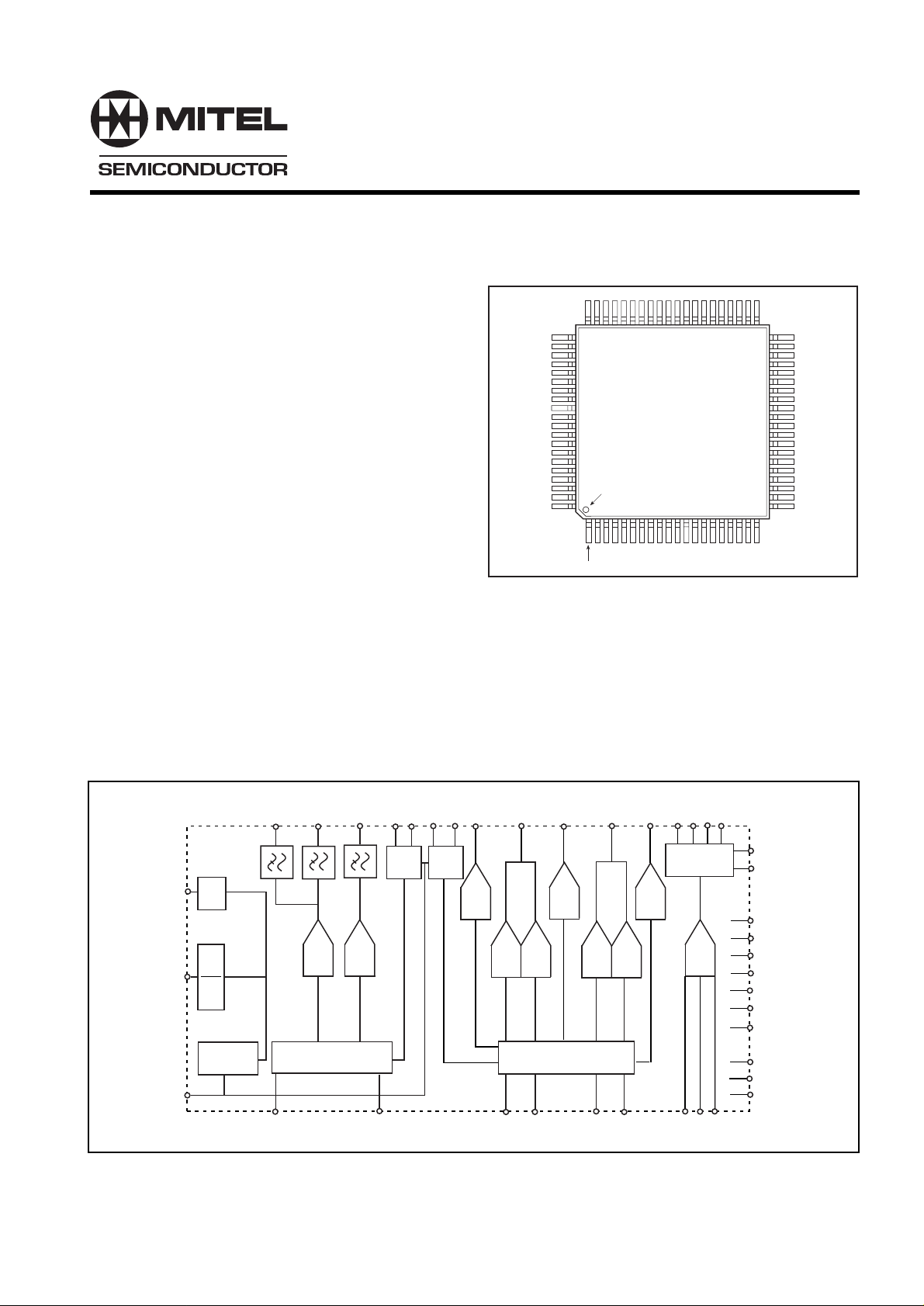
Figure 1 Pin connections - top view
MP28
GP80
TCXO/4
CHIPx8
TCXO
/4
1025
512
19.68MHz
BUFFER
TXQ,TXQ-
FM_MOD
8-BIT
DAC
tx calibration and control
TXI,TXI-
8-BIT
DAC
PD_RX
TXIF
PD_TX RXIF
TX
SYNTH
SYNTH
RX
8-BIT
DAC
FC_I
RXIFMDATATXD<7:0>TXCLK
8-BIT
ADC
Figure 2 Block diagram
I+,I- BAL Q+,Q-
8-BIT
DAC
6-BIT
ADC
rx calibration and control
RXQFMDATA
6-BIT
ADC
RXID<3:0>
FC_Q
8-BIT
DAC
8-BIT
ADC
RXQD<3:0>
ADC<3>
ADC<2>
ANALOG
MULTIPLEXER
ADCENA
ADCCLK
ADC<1>
8-BIT
ADC
ADC<0>
S<0>
S<1>
VDD
GND
SUB
FM/
SLEEP/
IDLE/
RESET/
SDATA
SCLOCK
SLATCH
ADCDATA
Page 2

PLUTO
PIN DESCRIPTION
No Pin Name Type A/D Description
1 VDD Power Power Supply
2 RSET Input Analog Bias current setting resistor - 40kΩ to ground
3 GND Ground Ground
4 TX_IF Input Analog TX VCO output
5 IDLEB Digital Idle mode control signal - active low - pulled low if left unconnected
6 PD TX Output TX synthesiser charge pump output
7 FMB Input Digital FM mode control signal - active low - pulled low if left unconnected
8 PD_RX Output Analog RX synthesiser charge pump output
9 SLEEPB Input Digital Sleep mode control signal - active low - pulled low if left unconnected
10 RX_IF Input Analog RX VCO output
11 TX_LOCK Output Digital TX synthesiser lock detect open drain output - pulled high by ext. resistor
12 RX_LOCK Output Digital RX synthesiser lock detect open drain output - pulled high by ext. resistor
13 TCXO/4 Output Digital TCXO divided by 4 output
14 TXD<0> Input Digital Transmit data bit 0 (lsb)
15 TXD<1> Input Digital Transmit data bit 1
16 TXD<2> Input Digital Transmit data bit 2
17 TXD<3> Input Digital Transmit data bit 3
18 TXD<4> Input Digital Transmit data bit 4
19 TXD<5> Input Digital Transmit data bit 5
20 TXD<6> Input Digital Transmit data bit 6
21 TXD<7> Input Digital Transmit data bit 7 (MSB)
22 TXCLK Input Digital Complimentary Transmit Clock (+ve)
23 TXCLKB Input Digital Complementary Transmit Clock (-ve)
24 CHIPx8 Input Digital 9.8304MHz synthesiser output
25 VDD Power Power Supply
26 TCXO Input Analog TCXO 19.68MHz a.c. coupled sinewave input
27 GND Ground Ground
28 SUB Ground Substrate-Ground
29 RESET Input Digital Chip master reset - pulled high if not connected
30 SDATA Input Digital Serial Interface Data Input
31 SCLK Input Digital Serial Interface Clock Input
32 SLATCH Input Digital Serial Interfce Latch Input
33 S<0> Input Digital Aux ADC mux channel select LSB
34 n/c
35 RXID<0> Output Digital I-Channel RX CDMA output LSB - low when inactive
36 RXID<1> Output Digital I-Channel RX CDMA output bit 1 - low when inactive
37 RXID<2> Output Digital I-Channel RX CDMA output bit 2 - low when inactive
38 RXID<3> Output Digital I-Channel RX CDMA output bit 3 - low when inactive
39 S<1> Input Digital Aux ADC mux channel select MSB
40 n/c
41 RXQD<0> Output Digital Q_Channel RX CDMA output LSB - low when inactive
42 RXQD<1> Output Digital Q_Channel RX CDMA output bit 1 - low when inactive
43 RXQD<2> Output Digital Q_Channel RX CDMA output bit 2 - low when inactive
44 RXQD<3> Output Digital Q_Channel RX CDMA output bit 3 - low when inactive
45 GND Ground Ground
46 VDD Power Power Supply
47 RXFMSTB input Digital Receive data FM strobe - pulled low if not connected
48 FMCLK Input Digital Receive data FM clock - pulled low if not connected
49 RXQFMDATA Output Digital Q-Channel RX FM data serial output - low when inactive
50 RXIFMDATA Output Digital I-Channel RX FM data serial output -low when inactive
51 ADCLK Output Digital Auxiliary ADC serial data clock. Low when inactive
52 ADCDATA Output Digital Auxiliary ADC serial data output. Low when inactive
53 ADCENA Input Digital Auxiliary ADC enable - pull down if not used
54 SUB Ground Substrate - Ground
2
Page 3

PIN DESCRIPTION (continued)
No Pin Name Type A/D Description
55 RXQP Input Analog Receive Q Channel Input (+ve)
56 RXQM Input Analog Receive Q Channel Input (-ve)
57 SUB Ground Substrate - Ground
58 RXIP Input Analog Receive Q channel input (+ve)
59 RXIM Input Analog Receive Q channel Input (-ve)
60 VDD Power Power Supply
61 GND Ground Ground
62 VREF<0> Input/Output Analog CDMA Receive Circuit Voltage Reference De-Coupling
63 AD<0> Input Analog AUX ADC Input
64 AD<1> Input Analog AUX ADC Input
65 AD<2> Input Analog AUX ADC Input
66 AD<3> Input Analog AUX ADC Input
67 Vtest Output Digital RX Filter tuning tone output - pulled low when inactive
68 EnTest Output Digital RX Filter tuning mode control output - pulled low when inactive
69 FC_Q Output Analog RX Filter Q channel FC control
70 FC_I Output Analog RX Filter channel FC control
71 BAL Output Analog RX Filter Gain Balance Control
72 VDD Power Power Supply
73 GND Ground Ground
74 TXIP Output Analog Transmit Circuit channel Complementary Output (+ve)
75 TXIM Output Analog Transmit Circuit I channel Complementary Output (-ve)
76 SUB Ground Substrate - Ground
77 TXQP Output Analog Transmit Circuit Q channel Complementary Output (+ve)
78 TXQM Output Analog Transmit Circuit Q channel Complementary Output (-ve)
79 FMTX Output Analog Transmit Circuit FM output
80 VREF<1> Input/Output Analog Transmit Circuit Voltage Reference De-coupling
PLUTO
FUNCTIONAL DESCRIPTION
Baseband TX interface circuit
The Pluto baseband transmit circuit acts as an interface
between the baseband signal processor and the RF/IF sections
in a CDMA/AMPS compatible mobile telephone.
The TX circuit has two modes of operation :
CDMA mode, transmit data that has previously been encoded
by the baseband digital signal processor is converted to
equivalent analog signals by matched digital-to-analog
converters, these signals are then filtered to remove the image
of the sample clock that would otherwise be present at the
output before being output to the I and Q modulator as
differential signals.
FM mode, transmit data is treated in much the same way as
in CDMA mode except that only one DAC is used and (because
of the much lower bandwidth of AMPS signals) a different
reconstruction filter is used before the analog fm signal is output
to the mixer as a single ended signal.
CDMA Transmit Signal Path
CDMA TX DACs
In CDMA mode two matched 8-bit DACs are used to
generate the in-phase and quadrature signals, the input
data for the DACs is obtained by multiplexing over an 8-bit
parallel input port (TXD<7:0>). The transmit data rate is
twice as fast as the differential transmit clock (TXCLK).
Incoming data that is valid during the rising edge of the
transmit clock is loaded into in In-Phase DAC & incoming
data that is valid on the falling edge of the transmit clock is
loaded into the Quadrature DAC - I and Q values must be
modified in the digital baseband chip to account for the halfcycle delay between them.
CDMA Analog Reconstruction Filters
The frequency spectrum at the output of the transmit
DACs contains unwanted frequency components.
Reconstruction filters are used to smooth the DAC output
signals, providing continuous time output signals at the I and
Q output pins thereby removing these undesirable signals.
The low pass filters used are 5th order Butterworth,
continuous time filters with a nominal cut-off frequency of 1.2
MHz. These filters are designed to have a linear phase
response in the pass band. On-chip reconstruction filters
minimise the phase and amplitude mismatch between I and
Q channels.
3
Page 4

PLUTO
CDMA TX Section Analog Interface
The ITx and QTx outputs can be d.c. or a.c. coupled to the
external circuits and will differentially drive a minimum
resistive load of 5 kΩ and a maximum capacitive load of 20 pF.
When the CDMA transmit path is in power-down mode the
positive outputs goes high and the negative output goes low.
FM Transmit Signal Path
FM TX DAC
In FM mode, the Q-Channel DAC is used to generate an
analog FM modulation signal from the data transmitted from
the digital baseband processor. In this mode, all other CDMA
TX circuits are powered down.
FM Mode Analog Reconstruction Filters
The frequency spectrum at the output of the transmit DAC
contains unwanted frequency components. A reconstruction
filter is used to smooth the DAC output signals.
Low-pass filters are used with a cut-off frequency of
approximately 13 kHz. These filters are 3rd order Butterworth
filters.
FM TX Section Analog Interface
The FMTX output can be d.c. or a.c. coupled to the radio
circuits and will drive a minimum resistive load of 5 kΩ and a
maximum capacitive load of 20 pF.
When the FM mode is in power-down the output is in high
impedance state.
CDMA Receive Signal Path
CDMA Receive ADC
In CDMA mode two high speed 4-bit ADCs are used to
digitise the incoming signals before subsequent transmission
to the baseband digital signal processor as two parallel 4 bit
words (RXI<3:0> and RXQ<3:0>). The sample rate of
9.8304MHz is generated via an on chip synthesiser that
requires no setting up or external components. On each falling
edge of the synthesised clock (CHIPx8) a new digital sample
is output on the digital bus.
CDMA Receive Calibration Circuit
On entering into CDMA mode from power down or from FM
mode the calibration circuits are activated. These circuits
measure the differences between the receive path gain in the
pass band and in the transition band of both I and Q filters. Via
a successive approximation process they tune the receive
filters cut-off frequency and amplitude matching using the 8 bit
DACs provided for this purpose (I_FC, Q_FC and BAL). Once
both filters (I and Q) have been calibrated in this way the DAC
outputs will not change until the chip is powered down or the
calibration circuit is re-activated in some other way.
FM Receive Signal Path
In FM mode two low speed 8-bit ADCs are used to digitise
the incoming signals before subsequent transmission to the
baseband digital signal processor as two serial 8-bit words
(FMRXI & FMRXQ). The sample rate is entirely determined by
the digital baseband processor (up-to the maximum allowed)
via the FMCLK input.
In FM mode the receive filters are assumed to track the
filters used in CDMA mode i.e. there is no separate tuning
mechanism.
SYNTHESISERS
The Synthesiser block comprises the input buffers, main
dividers, phase comparator, charge pump and lock detect
circuit for a TX and RX synthesiser. The loop filter components
and the VCOs are external to the device. A common reference
divider chain is also included together with bias and control
circuitry. All blocks apart from reference divider, bias and
control logic are duplicated exactly for RX and TX
synthesisers.
The receive intermediate frequency (RX_IF) is
programmable and the transmit intermediate frequency
(TX_IF) is fixed at 130.38MHz.
AUX ADC
The auxiliary converter section contains a single 8-bit
successive approximation analog to digital converter, with
serial output. In order to maximise the flexibility of Pluto, a 4
way analog multiplexer is provided, which enables the
converter to encode any one of four selectable channels. The
converter is intended for such applications as power supply
and temperature monitoring. When not in use, the converter is
powered down, and its outputs are held low.
4
Page 5

PLUTO
TIMING INFORMATION
Parameter Value Units Conditions
Min Typ Max
t1 TXCLOCK PERIOD (CDMA TX) 203.2 ns CDMA TX Figure 3
t2 TXCLOCK HIGH TIME (CDMA TX) 101.6 ns CDMA TX Figure 3
t3 TXCLOCK LOW TIME (CDMA TX) 101.6 ns CDMA TX Figure 3
t4 TXCLOCK PHASE Delay (CDMA TX) 1.2 ns CDMA TX Figure 3, FM TX Figure 4
t5 TXCLOCK RISE TIME (CDMA TX) 12 ns CDMA TX Figure 3, FM TX Figure 4
t6 TXCLOCK FALL TIME (CDMA TX) 12 ns CDMA TX Figure 3, FM TX Figure 4
t7 TXD-TXCLOCK SETUP TIME 20 ns CDMA TX Figure 3, FM TX Figure 4
t8 TXCLOCK-TXD HOLD TIME 3 ns CDMA TX Figure 3, FM TX Figure 4
t11 TXCLOCK PERIOD (FM TX) 2.78 µs FM TX Figure 4
t12 TXCLOCK HIGH TIME (FM TX) 1.39 µs FM TX Figure 4
t13 TXCLOCK LOW TIME (FM TX) 1.39 µs FM TX Figure 4
t14 CHIPx8 PERIOD 101.6 ns Figure 5
t15 CHIPx8 HIGH TIME 50.8 ns Figure 5
t16 CHIPx8LOW TIME 50.8 152.4 ns Figure 5
t17 CHIPx8 RISE TIME 3 12 ns Figure 5
t18 CHIPx8 FALL TIME 3 12 ns Figure 5
t19 RXD Hold Time After CHIPx8↓ 10 ns Figure 5
t20 RXD DELAY After CHIPx8↓ 20 ns Figure 5
t21 FMCLK PERIOD 2.78 µs FM RX Figure 6
t22 FMCLK HIGH TIME 1.39 µs FM RX Figure 6
t23 FMCLK LOW TIME 1.39 µs FM RX Figure 6
t24 FMCLK RISE TIME 12 ns FM RX Figure 6
t25 FMCLK FALL TIME 12 ns FM RX Figure 6
t26 RXFMSTB HIGH TIME 1 µs FM RX Figure 6
t27 RXFMSTB -FMCLK↓ SETUP TIME 50 ns FM RX Figure 6
t28 FMCLK↓ − RXFMSTB HOLD TIME 50 ns FM RX Figure 6
t29 FMCLK↓ − OUTPUT DATA DELAY 50 ns FM RX Figure 6
t30 ADCENA HIGH _ CONVERSION 40 µs General purpose ADC Figure 7
t31 ADCENA HIGH TIME 100 ns General purpose ADC Figure 7
t32 ADCENA LOW TIME 100 ns General purpose ADC Figure 7
t33 ADCCLK PERIOD 2.44 µs General purpose ADC Figure 7
t34 ADCCLK HIGH TIME 0.81 µs General purpose ADC Figure 7
t35 ADCCLK LOW TIME 1.62 µs General purpose ADC Figure 7
t36 ADCCLK RISE TIME 12 ns General purpose ADC Figure 7
t37 ADCCLK FALL TIME 12 ns General purpose ADC Figure 7
t38 ADCDATA VALID BEFORE ADCCLK↑ 1 µs General purpose ADC Figure 7
t39 ADC DATA HOLD TIME 5 ns General purpose ADC Figure 7
t40 SCLK-SDATA setup time 20 ns Serial Interface Figure 8
t41 SCLK-SDATA hold time 20 ns Serial Interface Figure 8
t42 SCLK pulse width 50 ns Serial Interface Figure 8
t43 SLATCH-SCLK setup time 20 ns Serial Interfsce Figure 8
t44 SLATCH pulse width 50 ns Serial Interface Figure 8
t45 SCLK period 100 ns Serial Interface Figure 8
5
Page 6

PLUTO
TXCLK
TXCLKbar
TXD<7:0>
TXCLK
t12
t2
t1
t3
t4
t5t4
t6
//
//
//
//
t7 t8
t9 t10
Figure 3 CDMA TX Mode
t11
t13
t4
t5t4
t6
TXCLKbar
TXD<7:0>
CHIPx8
RXQD<3:0>
RXID<3:0>
t15 t16
t14
t19
Figure 4. FM TX MODE
t17
t9 t10
t18
t20
Figure 5. CDMA RX MODE
6
Page 7

PLUTO
RXFMSTB
RXIFMDATA
RXQFMDATA
ADCENA
ADCCLK
FMCLK
t21
t22 t23
t31
t26
LSB-1 MSB
t29
Figure 6. FM RX MODE
t30
t32
t37
t34
t33
t35
t24
t25
t27 t28
LSB
t36
ADCDATA
SLATCH
SCLK
SDATA
MSB
t41
t45
MSB
t39t38
Figure 7. General purpose ADC
t42
Figure 8. Serial interface
LSB
t43t40
t44
LSB
7
Page 8

PLUTO
PROGRAMMING and CONTROL
The control modes for Pluto can be set via external pins or via a 3 wire serial interface. On initialising Pluto control is from
external pins but can then be set for programming from the serial interface by setting the appropriate bit in a serial input word.
The Rx second LO synthesiser is programmed via the serial interface: the Tx IF synthesiser is fixed and requires no programming.
Mode Control - External
The control modes are set by the pins SLEEPB, FMB and IDLEB as shown in the table below:
SLEEPB FMB IDLEB Mode
(Pin 9) (Pin 7) (Pin 5)
0 X X Sleep Mode
1 0 0 FM Receive only
1 0 1 FM Receive and Transmit
1 1 0 CDMA Receive only
1 1 1 CDMA Receive and Transmit
Aux ADC Selection - External
The auxiliary analog to digital converters can be selected via pins S0 and S1 as shown in the table below:
S1 S0 ADC
(Pin 39) (Pin 33) selected
0 0 ADC<0>
0 0 ADC<1>
1 0 ADC<2>
1 1 ADC<3>
ADC selection can also be programmed to be via serial interface if required
Serial Interface
The 3 wire serial interface (SDATA, SCLK and SLATCH) is programmed using 24 bit words as shown below. Timing
details are shown in Figure 8.
MSB LSB
23222120191817161514131211109876543210
WORD1 00000XXRXC RXDIV<13:0> 0 0
WORD2 SOP FMB IDB SLB 000000AD1AD0TST00000MXSCTB0001
X unused
RXC RX Synth comparison frequency :0 = 30kHz, 1 = 5kHZ
RXDIV<13:0> RX Synth divider ratio
SOP External/ Serial mode selection: 0 = Ext, 1 = Serial
SLB, IDB, FMB Sleep, Idle and FM mode control bits (serial mode)
TST Test Mode Control - This is for test purposes only and should be set to 0
AD1, AD0 Aux ADC select bits (serial mode)
MXS External / Serial Aux ADC select: 0 = Ext
CTB Enable Rx Calibration: 0 = calibration mode
If SOP is high mode control is via serial bits FMB, IDB and SLB, instead of external pins FMB, IDLEB and SLEEPB.
If MXS is high then ADC selection is via AD1, AD0 instead of S<1>, S<0>
8
Page 9

INITIALISATION
Transmit
On power-up or reset (RESETB) the Tx reconstruction
filters are tuned to give the specified cut-off frequency. This
calibration is internal and requires no external input. The
calibration time is 1ms.
Receive
On power-up or reset (RESETB) an autocalibration algorithm is started which can be used to tune the programmable
filters in Jupiter. (Jupiter is a programmable active filter designed for use in dual mode CDMA/AMPS system -further
details of which can be found in the Jupiter Datasheet). The
autocalibration is also initiated when Pluto is switched into
CDMA mode via FMB control.
PLUTO
When Pluto enters calibration mode the En Test (pin 68)
goes high. A test signal at 364kHz is then generated at the
Vtest output (pin 67). This signal is input to Jupiter which
provides a response which is digitised by the I and Q Rx ADCs.
An output DAC - BAL - (Pin 71) then tunes the Q channel to
match the I and Q channel amplitude via a successive approximation routine. The test signal is then switched to 728kHz
which is above the required cut off of the filter. DAC outputs,
FC_I and FC_Q are then adjusted to tune the I and Q filters to
the correct amplitude with reference to the in band test signal.
The filter cut off is tuned to 690kHz. Oversampling in the Rx
ADC's ensures sufficient accuracy for the calibration. This
calibration routine takes 26ms and after completion En Test
goes low and the test signal Vtest is disabled. Only the CDMA
filter is tuned, the matching within Jupiter ensures that the FM
(AMPS) filter performance meets specification.
0
-0.8
-4
Relative
Amplitude
(dB)
-5.8
CDMA TX FILTER RESPONSE
1k
Frequency (Hz)
630k 1.25M
Figure 9 Baseband RX interface circuit
10M
-0.6
Relative
Amplitude
(dB)
-3.0
0
FM TX FILTER RESPONSE
10k
29k
Frequency (Hz)
100k
9
Page 10

PLUTO
RECOMMENDED OPERATING CONDITIONS
Characteristic Value Units Conditions
Min Typ Max
Operating voltage range 2.7 3.6 V
Operating temperature range -40 +85 °C
Input high voltage, VIH VDD-0.8 V
Input low voltage, VIL 0.8 V
Master clock amplitude 800 mV pk-pk AC coupled 19.68MHz sinusoidal
signal
Input current, IIH 0.1 µA
Input capacitance, CIN 5 pF
Output high voltage, VOH VDD-0.4 V IOUT = 100µA
Output low voltage, VOL 0.4 V IOUT = 100µA
Tri-state leakage current 10 µA
ELECTRICAL CHARACTERISTICS
T
= -30°C to +70°C, V
AMB
apply within the specified ambient temperature and supply voltage ranges unless otherwise stated.
= +2.7 to +3.6V. These characteristics are guaranteed by either production test or design. They
CC
Characteristic Value Units Conditions
Min Typ Max
CDMA TX Interface
Resolution 8 Bits
Integral non-linearity 0.5 LSB
Differential non-linearity 0.5 LSB
Full scale output Voltage 1.6 2.05 2.4 V Vpp differential
Output common mode Voltage 1.1 1.2 1.3 V
+Ve output Voltage in Power-down mode Vdd-0.16 Vdd-0.1 Vdd-0.04 V
-Ve output Voltage in Power-down mode 0.04 0.1 0.16 V
I,Q gain mismatch 0.15 dB
I,Q phase imbalance 1 degrees
Differential offset TBD mV
PSRR 50 dB VDD to differential I & Q outputs,
100mV pk-pk at 100kHz
Load resistance 5 kΩ
Load capacitance 20 pF
Filter type Butterwoth low pass
Filter order 5th
Filter cut off See Figure 9
Filter Pass Band ripple See Figure 9
Filter stop band attenuation See Figure 9
Sample rate 6 Msample/s
10
Page 11

ELECTRICAL CHARACTERISTICS (continued)
T
= -30°C to +70°C, V
AMB
apply within the specified ambient temperature and supply voltage ranges unless otherwise stated.
Characteristic Value Units Conditions
FM TX Interface
Resolution 8 Bits
Integral non linearity 0.5 LSB
Differential non linearity 0.5 LSB
Output Voltage range 550 mVpp
Output Voltage mid scale 0 V Differential
PSRR 50 dB Vdd to output, 100mV
Load resistance 5 kΩ
Load capacitance 20 pF
Filter type Butterworth low pass
Filter order 3rd
Filter Pass Band ripple See Figure 9
Filter stop band attenuation See Figure 9
Filter cut-off See Figure 9
CDMA RX Interface
Resolution 4 Bits
Full scale input voltage 1 V pk-pk Measured differentially
Input common mode range Vdd -1.4 V
Input sample rate 9.8304 Ms/s
Input resistance (dc) 20 kΩ
Input capacitance 10 20 pF
Integral non linearity 0.15 LSB
Differential non linearity 0.175 LSB
IRX and QRX gain matching 0.25 dB
= +2.7 to +3.6V. These characteristics are guaranteed by either production test or design. They
CC
Min Typ Max
pk-pk at 100kHz
PLUTO
11
Page 12

PLUTO
ELECTRICAL CHARACTERISTICS (CDMA BASEBAND RX INTERFACE CIRCUIT) continued
T
= -30°C to +70°C, V
AMB
apply within the specified ambient temperature and supply voltage ranges unless otherwise stated.
Characteristic Value Units Conditions
FM RX Interface
Resolution 8 Bits
Full scale input voltage 1 V pk-pk Measured differentially
Input dc level Vdd-1.4 V
Input sample rate 30 50 ks/s
Input resistance (dc) 100 kΩ
Input capacitance 10 20 pF
Integral non linearity ±1.5 LSB
Differential non linearity ±0.75 LSB
AUXILIARY CONVERTER SECTION
Resolution 8 Bits
ADC full scale range 2.5 V
ADC zero scale range 0.5 V
Integral non linearity ±1.25 LSB
Differential non linearity ±0.75 LSB
Conversion time 20 ks/s
ADCCLK 410 kHz
= +2.7 to +3.6V. These characteristics are guaranteed by either production test or design. They
CC
Min Typ Max
12
Page 13

ELECTRICAL CHARACTERISTICS (Continued)
T
= -30°C to +70°C, V
AMB
apply within the specified ambient temperature and supply voltage ranges unless otherwise stated.
Characteristic Value Units Conditions
TRANSMIT SYNTHESISER
Input Frequency 65.19 MHz
Lock mode output current current 16 µA Rset = 40kΩ
Acquisition mode output current 176 µA Rset = 40kΩ
PD output compliance 0.5 Vdd-0.5 V
RECEIVER SYNTHESISER
Input frequency 42.69 52.595 MHz
Lock mode output current 16 µA Rset = 40kΩ
Acquisition mode output current 176 V Rset = 40kΩ
PD output compliance 0.5 Vdd-0.5 V
POWER SUPPLY CURRENTS
Sleep 1 mA
CDMA_IDLE 11 15 mA
FM_ILDE 5 7 mA
CDMA_RTTX 18 32 mA
FM_RXTX 11 15 mA
= +2.7 to +3.6V. These characteristics are guaranteed by either production test or design. They
CC
Min Typ Max
PLUTO
13
Page 14

Page 15

http://www.mitelsemi.com
World Headquarters - Canada
Tel: +1 (613) 592 2122
Fax: +1 (613) 592 6909
North America Asia/Pacific Europe, Middle East,
Tel: +1 (770) 486 0194 Tel: +65 333 6193 and Africa (EMEA)
Fax: +1 (770) 631 8213 Fax: +65 333 6192 Tel: +44 (0) 1793 518528
Fax: +44 (0) 1793 518581
Information relating to products and services furnished herein by Mitel Corporation or its subsidiaries (collectively “Mitel”) is believed to be reliable. However, Mitel assumes no
liability for errors that may appear in this publication, or for liability otherwise arising from the application or use of any such information, product or service or for any infringement of
patents or other intellectual property rights owned by third parties which may result from such application or use. Neither the supply of such information or purchase of product or
service conveys any license, either express or implied, under patents or other intellectual property rights owned by Mitel or licensed from third parties by Mitel, whatsoever.
Purchasers of products are also hereby notified that the use of product in certain ways or in combination with Mitel, or non-Mitel furnished goods or services may infringe patents or
other intellectual property rights owned by Mitel.
This publication is issued to provide information only and (unless agreed by Mitel in writing) may not be used, applied or reproduced for any purpose nor form part of any order or
contract nor to be regarded as a representation relating to the products or services concerned. The products, their specifications, services and other information appearing in this
publication are subject to change by Mitel without notice. No warranty or guarantee express or implied is made regarding the capability, performance or suitability of any product or
service. Information concerning possible methods of use is provided as a guide only and does not constitute any guarantee that such methods of use will be satisfactory in a specific
piece of equipment. It is the user’s responsibility to fully determine the performance and suitability of any equipment using such information and to ensure that any publication or
data used is up to date and has not been superseded. Manufacturing does not necessarily include testing of all functions or parameters. These products are not suitable for use in
any medical products whose failure to perform may result in significant injury or death to the user. All products and materials are sold and services provided subject to Mitel’s
conditions of sale which are available on request.
M Mitel (design) and ST-BUS are registered trademarks of MITEL Corporation
Mitel Semiconductor is an ISO 9001 Registered Company
Copyright 1999 MITEL Corporation
All Rights Reserved
Printed in CANADA
TECHNICAL DOCUMENTATION - NOT FOR RESALE
 Loading...