

Page 1
Philips Semiconductors Programmable Logic Devices Product specification
PLS153/A
Programmable logic arrays
(18 × 42 × 10)
1
October 22, 1993 853–0311 11164
DESCRIPTION
The PLS153 and PLS153A are two-level
logic elements, consisting of 42 AND gates
and 10 OR gates with fusible link connections
for programming I/O polarity and direction.
All AND gates are linked to 8 inputs (I) and
10 bidirectional I/O lines (B). These yield
variable I/O gate configurations via 10
direction control gates (D), ranging from 18
inputs to 10 outputs.
On-chip T/C buffers couple either True (I, B)
or Complement (I
, B) input polarities to all
AND gates, whose outputs can be optionally
linked to all OR gates. Their output polarity, in
turn, is individually programmable through a
set of EX-OR gates for implementing
AND/OR or AND/NOR logic functions.
The PLS153 and PLS153A are
field-programmable, enabling the user to
quickly generate custom patterns using
standard programming equipment.
FEATURES
•Field-Programmable (Ni-Cr links)
•8 inputs
•42 AND gates
•10 OR gates
•10 bidirectional I/O lines
•Active-High or -Low outputs
•42 product terms:
– 32 logic terms
– 10 control terms
•I/O propagation delay:
– PLS153: 40ns (max)
– PLS153A: 30ns (max)
•Input loading: –100µA (max)
•Power dissipation: 650mW (typ)
•3-State outputs
•TTL compatible
APPLICATIONS
•Random logic
•Code converters
•Fault detectors
•Function generators
•Address mapping
•Multiplexing
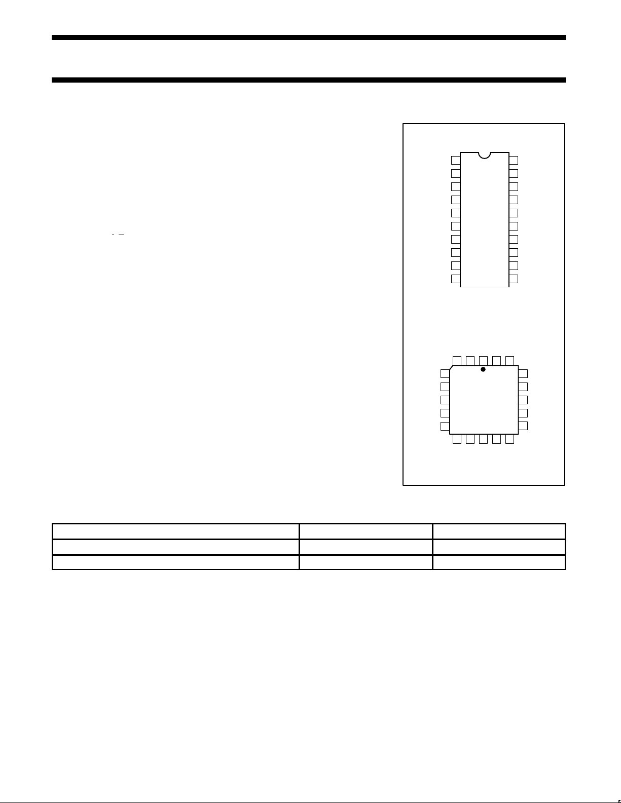
PIN CONFIGURATIONS
1
2
3
4
5
6
7
8
9
10 11
12
13
14
15
16
17
18
19
20
N Package
I
0
I
1
I
2
I
3
I
4
I
5
I
6
I
7
B
0
B
2
GND
B
3
B
4
B
5
B
6
B
7
B
8
B
9
V
CC
B
1
123
4
5
6
7
8
9 10 11 12 13
14
15
16
17
18
1920
A Package
N = Plastic DIP (300mil-wide)
A = Plastic Leaded Chip Carrier
B
2B3
B
4
B
5
B
6
B
7
B
8
B9V
CC
B
1
I0I1I
2
I
3
I
4
I
5
I
6
I
7
B
0
GND
SP00274
ORDERING INFORMATION
DESCRIPTION ORDER CODE DRAWING NUMBER
20-Pin Plastic Dual In-Line, 300mil-wide PLS153N, PLS153AN 0408B
20-Pin Plastic Leaded Chip Carrier PLS153A, PLS153AA 0400E
Page 2

Philips Semiconductors Programmable Logic Devices Product specification
PLS153/A
Programmable logic arrays
(18 × 42 × 10)
October 22, 1993
2
LOGIC DIAGRAM
NOTES:
1. All programmed ‘AND’ gate locations are pulled to logic “1”.
2. All programmed ‘OR’ gate locations are pulled to logic “0”.
3. Programmable connection.
(LOGIC TERMS–P) (CONTROL TERMS)
1
2
3
4
5
6
7
8
9
11
12
13
14
15
16
17
18
19
I0
I1
I2
I3
I4
I5
I6
I7
B9
B8
B7
B6
B5
B4
B3
B2
B1
B0
31 24 23 16 15 8 7 0
D9D8D7D6D5D4D3D2D1D
0
S
9
S
8
S
7
S
6
S
5
S
4
S
3
S
2
S
1
S
0
X
9
X
8
X
7
X
6
X
5
X
4
X
3
X
2
X
1
X
0
B9
B8
B7
B6
B5
B4
B3
B2
B1
B0
SP00276
Page 3

Philips Semiconductors Programmable Logic Devices Product specification
PLS153/A
Programmable logic arrays
(18 × 42 × 10)
October 22, 1993
3
FUNCTIONAL DIAGRAM
P
31
P
0
D
0
D
9
I
0
I
7
B
0
B
9
B
9
B
0
S
0
S
9
X
9
X
0
SP00277
ABSOLUTE MAXIMUM RA TINGS
1
RATINGS
SYMBOL PARAMETER MIN MAX UNIT
V
CC
Supply voltage +7 V
DC
V
IN
Input voltage +5.5 V
DC
V
OUT
Output voltage +5.5 V
DC
I
IN
Input currents –30 +30 mA
I
OUT
Output currents +100 mA
T
amb
Operating temperature range 0 +75 °C
T
stg
Storage temperature range –65 +150 °C
NOTES:
1. Stresses above those listed may cause malfunction or permanent damage to the device. This
is a stress rating only. Functional operation at these or any other condition above those
indicated in the operational and programming specification of the device is not implied.
Page 4

Philips Semiconductors Programmable Logic Devices Product specification
PLS153/A
Programmable logic arrays
(18 × 42 × 10)
October 22, 1993
4
LOGIC FUNCTION
NOTES:
1. For each of the 10 outputs, either function Z
(Active-High) or Z
(Active-Low) is available, but not
both. The desired output polarity is programmed via
the Ex-OR gates.
2. Z, A, B, C, etc. are user defined connections to fixed
inputs (I) and bidirectional pins (B).
TYPICAL PRODUCT TERM:
Pn = A
⋅ B ⋅ C ⋅ D ⋅ . . .
TYPICAL LOGIC FUNCTION:
AT OUTPUT POLARITY = H
Z = P0 + P1 + P2 . . .
AT OUTPUT POLARITY = L
Z = P0 + P1 + P2 +
. . .
Z = P0
⋅ P1 ⋅ P2 ⋅ . . .
SP00275
THERMAL RATINGS
TEMPERATURE
Maximum junction
150C
Maximum ambient
75C
Allowable thermal rise
ambient to junction
75C
The PLS153/A devices are also processed to
military requirements for operation over the
military temperature range. For specifications
and ordering information consult the Philips
Semiconductors Military Data Handbook.
DC ELECTRICAL CHARACTERISTICS
0°C ≤ T
amb
≤ +75°C, 4.75V ≤ VCC ≤ 5.25V
LIMITS
SYMBOL PARAMETER TEST CONDITIONS MIN TYP
1
MAX UNIT
Input voltage
2
V
IL
Low VCC = MIN 0.8 V
V
IH
High VCC = MAX 2.0 V
V
IC
Clamp
3
VCC = MIN, IIN = –12mA –0.8 –1.2 V
Output voltage
2
VCC = MIN
V
OL
Low
4
IOL = 15mA 0.5 V
V
OH
High
5
IOH = –2mA 2.4 V
Input current
9
VCC = MAX
I
IL
Low VIN = 0.45V –100 µA
I
IH
High VIN = 5.5V 40 µA
Output current
VCC = MAX
I
O(OFF)
Hi-Z state
8
V
OUT
= 5.5V 80 µA
V
OUT
= 0.45V –140
I
OS
Short circuit
3, 5, 6
V
OUT
= 0V –15 –70 mA
I
CC
VCC supply current
7
VCC = MAX 130 155 mA
Capacitance
VCC = 5V
C
IN
Input VIN = 2.0V 8 pF
C
B
I/O VB = 2.0V 15 pF
NOTES:
1. All typical values are at V
CC
= 5V, T
amb
= +25°C.
2. All voltage values are with respect to network ground terminal.
3. Test one at a time.
4. Measured with +10V applied to I
7
.
5. Measured with +10V applied to I
0–7
. Output sink current is supplied through a resistor to VCC.
6. Duration of short circuit should not exceed 1 second.
7. I
CC
is measured with I0, I1 at 0V, I2 – I7 and B
0–9
at 4.5V.
8. Leakage values are a combination of input and output leakage.
9. I
IL
and IIH limits are for dedicated inputs only (I0 – I7).
Page 5

Philips Semiconductors Programmable Logic Devices Product specification
PLS153/A
Programmable logic arrays
(18 × 42 × 10)
October 22, 1993
5
AC ELECTRICAL CHARACTERISTICS
0°C ≤ T
amb
≤ +75°C, 4.75V ≤ VCC ≤ 5.25V , R1 = 300Ω, R2 = 390Ω
LIMITS
SYMBOL PARAMETER FROM TO TEST PLS153 PLS153A UNIT
CONDITION MIN TYP1MAX MIN TYP1MAX
t
PD
Propagation delay Input ± Output ± CL = 30pF 30 40 20 30 ns
t
OE
Output enable
2
Input ± Output – CL = 30pF 25 35 20 30 ns
t
OD
Output disable
2
Input ± Output + CL = 5pF 25 35 20 30 ns
NOTES:
1. All typical values are at V
CC
= 5V, T
amb
= +25°C.
2. For 3-State output; output enable times are tested with CL = 30pF to the 1.5V level, and S1 is open for high-impedance to High tests and
closed for high-impedance to Low tests. Output disable times are tested with C
L
= 5pF. High-to-High impedance tests are made to an output
voltage of V
T
= (VOH – 0.5V) with S1 open, and Low-to-High impedance tests are made to the VT = (VOL + 0.5V) level with S1 closed.
3. All propagation delays are measured and specified under worst case conditions.
VOLTAGE WAVEFORMS
90%
10%
5ns5ns
5ns 5ns
90%
10%
+3.0V
+3.0V
0V
0V
t
RtF
MEASUREMENTS:
All circuit delays are measured at the +1.5V level of
inputs and outputs, unless otherwise specified.
Input Pulses
SP00017
TIMING DEFINITIONS
SYMBOL PARAMETER
t
PD
Propagation delay between
input and output.
t
OD
Delay between input change
and when output is off (Hi-Z
or High).
t
OE
Delay between input change
and when output reflects
specified output level.
TEST LOAD CIRCUIT
+5V
C
L
R
1
R
2
S
1
GND
B
Z
B
Y
INPUTS
I
0
I
7
B
W
B
X
OUTPUTS
C
2
C
1
DUT
NOTE:
C
1
and C2 are to bypass VCC to GND.
V
CC
SP00278
Page 6

Philips Semiconductors Programmable Logic Devices Product specification
PLS153/A
Programmable logic arrays
(18 × 42 × 10)
October 22, 1993
6
TIMING DIAGRAM
+3V
0V
V
OH
V
OL
I, B
B
t
PD
1.5V 1.5V 1.5V
1.5V 1.5V
t
OD
t
OE
V
T
SP00279
CODEACTIVE LEVEL
LOW
(INVERTING)
L
CODEACTIVE LEVEL
HIGH
1
(NON–INVERTING)
H
S
X
B
S
X
B
SP00280
CODE
O
STATE
INACTIVE
1, 2
CODESTATE CODESTATE CODESTATE
I, B
H
L –
P, D
I, B
I, B
I, B
I, B
P, D
I, B
I, B
I, B
P, D
I, B
I, B
I, B
P, D
I, B
I, B
I, B
DON’T CARE
SP00281
ABEL is a trademark of Data I/O Corp.
CUPL is a trademark of Logical Devices, Inc.
LOGIC PROGRAMMING
The PLS153/A is fully supported by industry
standard (JEDEC compatible) PLD CAD
tools, including Philips Semiconductors
SNAP, Data I/O’s ABEL and Logical
Devices, Inc. CUPL design software
packages.
All packages allow Boolean and state
equation entry formats. SNAP, ABEL and
CUPL also accept, as input, schematic
capture format.
PLS153/A logic designs can also be
generated using the program table entry
format detailed on the following page. This
program table entry format is supported by
the Philips Semiconductors SNAP PLD
design software package.
To implement the desired logic functions, the
state of each logic variable from logic
equations (I, B, O, P, etc.) is assigned a
symbol. The symbols for TRUE,
COMPLEMENT, INACTIVE, PRESET, etc.,
are defined below.
PROGRAMMING/SOFTWARE
SUPPORT
Refer to Section 9
and Section 10
Software Support)
additional information
(Development Software)
(Third-Party Programmer/
of this data handbook for
OUTPUT POLARITY – (B)
AND ARRAY – (I, B)
Page 7

Philips Semiconductors Programmable Logic Devices Product specification
PLS153/A
Programmable logic arrays
(18 × 42 × 10)
October 22, 1993
7
OR ARRAY – (B)
CODE
INACTIVE
A
CODE
P
n
STATUS
ACTIVE
1
•
P
S
P
n
STATUS
P
S
SP00282
NOTES:
1. This is the initial unprogrammed state of
all links.
2. Any gate P
if both the True and Complement of an input
(either I or B) are left intact.
VIRGIN STATE
A factory shipped virgin device contains all
fusible links intact, such that:
1. All outputs are at “H” polarity.
2. All P
3. All P
will be unconditionally inhibited
n
terms are disabled.
n
terms are active on all outputs.
n
CAUTION: PLS153A TEST
COLUMNS
The PLS153A incorporates two columns not
shown in the logic block diagram. These
columns are used for in-house testing of the
device in the unprogrammed state. These
columns must be disabled prior to using the
PLS153A in your application. If you are using
a Philips Semiconductors-approved
programmer, the disabling is accomplished
during the device programming sequence. If
these columns are not disabled, abnormal
operation is possible.
Furthermore, because of these test columns,
the PLS153A cannot be programmed using
the programmer algorithm for the PLS153.
Page 8

Philips Semiconductors Programmable Logic Devices Product specification
PLS153/A
Programmable logic arrays
(18 × 42 × 10)
October 22, 1993
8
PROGRAM TABLE
8
POLARITY
1
2
3
4
5
6
7
8
9
10
11
12
13
14
15
16
17
18
19
20
21
22
23
24
25
26
27
28
29
30
31
D9
D8
D7
D6
D5
D4
D3
D2
D1
D0
PIN
T
E
R
M
AND OR
ACTIVE
INACTIVE
CONTROL
HIGH
LOW
A
INACTIVE
H
L
B(0)
(POL)
DON’T CARE
I, B
I, B
I, B(I)
CUSTOMER NAME
PHILIPS DEVICE #
PROGRAM TABLE # REV DATE
0HL
—
VARIABLE
NAME
AND OR
B(0)
7 6 5 4 3 2 1 0 9 8 7 6 5 4 3 2 1 0 9 8 7 6 5 4 3 2 1 0
B(I)
7 6 5 4 3 2 1 19 18 17 16 15 14 13 12 11 9 19 18 17 16 15 14 13 12 11 9
PURCHASE ORDER #
CF(XXXX)
CUSTOMER SYMBOLIZED PART #
TOTAL NUMBER OF PARTS
I
0
NOTES
In the unprogrammed state:
Output polarity is non–inverting.
Unused I and B bits in the AND array should be programmed
Unused product terms in the OR array should be
as Don’t Care (–).
All AND gates are pulled to a logic “0” (Low).
programmed as INACTIVE (o).
SP00283
Page 9

Philips Semiconductors Programmable Logic Devices Product specification
PLS153/A
Programmable logic arrays
(18 × 42 × 10)
October 22, 1993
9
SNAP RESOURCE SUMMARY DESIGNATIONS
CAND
P
31
P
0
D
0
D
9
I0
I7
B0
B9
B9
B0
S
0
S
9
X
9
X
0
DIN153
NIN153
OR
TOUT153
AND
EXOR153
DIN153
NIN153
SP00284
 Loading...