

Page 1

Philips Semiconductors Programmable Logic Devices Product specification
PLS100/PLS101
Programmable logic arrays
(16 × 48 × 8)
49
October 22, 1993 853–0308 11164
DESCRIPTION
The PLS100 (3-State) and PLS101 (Open
Collector) are bipolar, fuse Programmable
Logic Arrays (PLAs). Each device utilizes the
standard AND/OR/Invert architecture to
directly implement custom sum of product
equations.
Each device consists of 16 dedicated inputs
and 8 dedicated outputs. Each output is
capable of being actively controlled by any or
all of the 48 product terms. The True,
Complement, or Don’t Care condition of each
of the 16 inputs and be ANDed together to
comprise one P-term. All 48 P-terms can be
selectively ORed to each output.
The PLS100 and PLS101 are fully TTL
compatible, and chip enable control for
expansion of input variables and output
inhibit. They feature either Open Collector or
3-State outputs for ease of expansion of
product terms and application in
bus-organized systems.
Order codes are listed in the Ordering
Information Table.
FEATURES
•Field-programmable (Ni-Cr link)
•Input variables: 16
•Output functions: 8
•Product terms: 48
•I/O propagation delay: 50ns (max.)
•Power dissipation: 600mW (typ.)
•Input loading: –100µA (max.)
•Chip Enable input
•Output option:
– PLS100: 3-State
– PLS101: Open-Collector
•Output disable function:
– 3-State: Hi-Z
– Open-Collector: High
APPLICATIONS
•CRT display systems
•Code conversion
•Peripheral controllers
•Function generators
•Look-up and decision tables
•Microprogramming
•Address mapping
•Character generators
•Data security encoders
•Fault detectors
•Frequency synthesizers
•16-bit to 8-bit bus interface
•Random logic replacement
PIN CONFIGURATIONS
1
2
3
4
5
6
7
8
9
10
11
12
13
14 15
16
17
18
19
20
21
22
23
24
25
26
27
28
N Package
FE*
I7
I6
I5
I4
I3
I2
I1
I0
F7
F6
F5
F4
GND
V
CC
I8
I9
I10
I11
I12
I14
CE
F0
F1
F2
F3
I15
I13
1234
5
6
7
8
9
10
11
12 13 14 15 16 17
18
19
20
21
22
23
24
25
262728
FE
A Package
F7
I7I6I5
I4
I3
I2
I1
I0
F6
F5 F4
GND
F2
F1 F0
I9I8
V
CC
F3
CE
I10
I11
I12
I14
I15
I13
* Fuse Enable Pin: It is recommended that this pin
be left open or connected to ground during normal
operation.
N = Plastic DIP (600mil-wide)
A = Plastic Leaded Chip Carrier
ORDERING INFORMATION
DESCRIPTION 3-STATE OPEN COLLECTOR DRAWING NUMBER
28-Pin Plastic Dual In-Line 600mil-wide PLS100N PLS101N 0413D
28-Pin Plastic Leaded Chip Carrier PLS100A PLS101A 0401F
Page 2

Philips Semiconductors Programmable Logic Devices Product specification
PLS100/PLS101
Programmable logic arrays
(16 × 48 × 8)
October 22, 1993
50
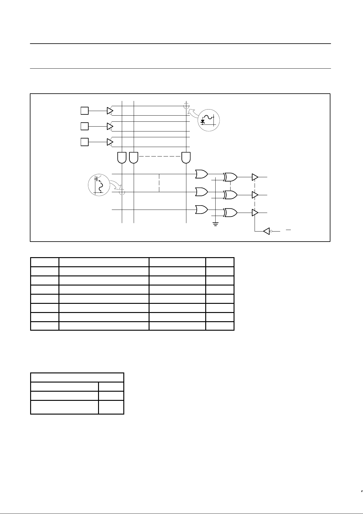
LOGIC DIAGRAM
NOTES:
1. All AND gate inputs with a blown link float to a logic “1”.
2. All OR gate inputs with a blown fuse float to logic “0”.
3. Programmable connection.
(LOGIC TERMS–P)
9
8
7
6
5
4
3
2
10
11
12
13
15
16
17
18
I0
I1
I2
I3
I4
I5
I6
I7
F0
F1
F2
F3
F4
F5
F6
F7
47 40 39 32 31 24 23 16
S
0
S
1
S
2
S
3
S
4
S
5
S
6
S
7
X
0
X
1
X
2
X
3
X
4
X
5
X
6
X
7
8 7 0
27
26
25
24
23
22
21
20
I8
I9
I10
I11
I12
I13
I14
I15
19
CE
15
Page 3
Philips Semiconductors Programmable Logic Devices Product specification
PLS100/PLS101
Programmable logic arrays
(16 × 48 × 8)
October 22, 1993
51
FUNCTIONAL DIAGRAM
I0
I1
I15
TYPICAL CONNECTION
TYPICAL CONNECTION
P
0P1
P
47
S
0
S
6
S
7
F0
F6
F7
CE
ABSOLUTE MAXIMUM RATINGS
1
SYMBOL
PARAMETER RATINGS UNIT
V
CC
Supply voltage +7.0 V
DC
V
IN
Input voltage +5.5 V
DC
V
O
Output voltage +5.5 V
DC
I
IN
Input current ±30 mA
I
OUT
Output current +100 mA
T
amb
Operating temperature range 0 to +75 °C
T
stg
Storage temperature range –65 to +150 °C
NOTE:
1. Stresses above those listed may cause malfunction or permanent damage to the device.
This is a stress rating only. Functional operation at these or any other conditions above
those indicated in the operational and programming specification of the device is not
implied.
THERMAL RATINGS
TEMPERATURE
Maximum junction 150°C
Maximum ambient 75°C
Allowable thermal rise
ambient to junction
75°C
The PLS100 device is also processed to
military requirements for operation over the
military temperature range. For specifications
and ordering information consult the Philips
Semiconductors Military Data Handbook.
Page 4

Philips Semiconductors Programmable Logic Devices Product specification
PLS100/PLS101
Programmable logic arrays
(16 × 48 × 8)
October 22, 1993
52
DC ELECTRICAL CHARACTERISTICS
0°C ≤ T
amb
≤ +75°C, 4.75V ≤ VCC ≤ 5.25V
LIMITS
SYMBOL PARAMETER TEST CONDITIONS MIN TYP
1
MAX UNIT
Input voltage
2
V
IH
High VCC = MAX 2.0 V
V
IL
Low VCC = MIN 0.8 V
V
IC
Clamp
3
VCC = MIN, IIN = –12mA –0.8 –1.2 V
Output voltage
2
VCC = MIN
V
OH
High (PLS100)
4
IOH = –2mA 2.4 V
V
OL
Low
5
IOL = 9.6mA 0.35 0.45 V
Input current
I
IH
High VIN = 5.5V < 1 25 µA
I
IL
Low VIN = 0.45V –10 –100 µA
Output current
I
O(OFF)
Hi-Z state (PLS100) CE = High, VCC = MAX
V
OUT
= 5.5V 1 40 µA
V
OUT
= 0.45V –1 –40 µA
I
OS
Short circuit (PLS100)
3, 6
CE = Low, V
OUT
= 0V –15 –70 mA
I
CC
VCC supply current
7
VCC = MAX 120 170 mA
Capacitance
CE = High, VCC = 5.0V
C
IN
Input VIN = 2.0V 8 pF
C
OUT
Output V
OUT
= 2.0V 17 pF
NOTES:
1. All typical values are at V
CC
= 5V, T
amb
= +25°C.
2. All voltage values are with respect to network ground terminal.
3. Test one pin at a time.
4. Measured with V
IL
applied to CE and a logic high stored.
5. Measured with a programmed logic condition for which the output test is at a low logic level. Output sink current is applied through a resistor
to V
CC
.
6. Duration of short circuit should not exceed 1 second.
7. I
CC
is measured with the Chip Enable input grounded, all other inputs at 4.5V and the outputs open.
Page 5

INPUT
F0 – F7
CE
1.5V
1.5V 1.5V
1.5V 1.5V
t
PD
t
CE
t
CD
V
OL
V
OH
+3.0V
0V
+3.0V
0V
Read Cycle
Philips Semiconductors Programmable Logic Devices Product specification
PLS100/PLS101
Programmable logic arrays
(16 × 48 × 8)
October 22, 1993
53
AC ELECTRICAL CHARACTERISTICS
0°C < T
amb
< +75°C, 4.75 < VCC < 5.25V, R1 = 470Ω, R2 = 1kΩ
LIMITS
SYMBOL PARAMETER TO FROM MIN TYP
1
MAX UNIT
Propagation delay
2
t
PD
Input Output Input 35 50 ns
t
CE
Chip Enable
3
Output Chip Enable 15 30 ns
Disable time
t
CD
Chip Disable
3
Output Chip Enable 15 30 ns
NOTES:
1. All typical values are at V
CC
= 5V. T
amb
= +25°C.
2. All propagation delays are measured and specified under worst case conditions.
3. For 3-State output; output enable times are tested with C
L
= 30pF to the 1.5V level, and S1 is open for high-impedance to High tests and
closed for high-impedance to Low tests. Output disable times are tested with C
L
= 5pF. High-to-High impedance tests are made to an output
voltage of V
T
= (VOH – 0.5V) with S1 open, and Low-to-High impedance tests are made to the VT = (VOL + 0.5V) level with S1 closed.
VOLTAGE WAVEFORMS TEST LOAD CIRCUIT
MEASUREMENTS:
All circuit delays are measured at the +1.5V level of inputs and outputs, unless otherwise specified.
90%
10%
5ns5ns
5ns 5ns
90%
10%
+3.0V
+3.0V
0V
0V
t
RtF
Input Pulses
+5V
C
L
R
1
R
2
S
1
GND
F
7
F
0
INPUTS
I
0
I
15
CE
OUTPUTS
C
2
C
1
DUT
NOTE:
C
1
and C2 are to bypass VCC to GND.
V
CC
TIMING DEFINITIONS
SYMBOL PARAMETER
t
CE
Delay between beginning of
Chip Enable Low (with Input
valid) and when Data Output
becomes valid.
t
CD
Delay between when Chip
Enable becomes High and
Data Output is in off state
(Hi-Z or High).
t
PD
Delay between beginning of
valid Input (with Chip Enable
Low) and when Data Output
becomes valid.
TIMING DIAGRAM
Page 6

Philips Semiconductors Programmable Logic Devices Product specification
PLS100/PLS101
Programmable logic arrays
(16 × 48 × 8)
October 22, 1993
54
LOGIC PROGRAMMING
PLS100/PLS101 is fully supported by
industry standard (JEDEC compatible) PLD
CAD tools, including Philips Semiconductors’
SNAP, Data I/O Corporation’s ABEL and
Logical Devices Inc.’s CUPL design
software packages.
All packages allow Boolean and state
equation entry formats. SNAP, ABEL and
CUPL also accept, as input, schematic
capture format.
PLS100/PLS101 logic designs can also be
generated using the program table entry
format detailed on the following pages. This
program table entry format is supported by
the Philips Semiconductors’ SNAP PLD
design software package.
To implement the desired logic functions, the
state of each logic variable from logic
equations (I, B, O, P, etc.) is assigned a
symbol. The sumbols for TRUE,
COMPLEMENT, INACTIVE, PRESET, etc.,
are defined below.
PROGRAMMING AND
SOFTWARE SUPPORT
Refer to Section 9
(Development Software)
and Section 10
(Third-party Programmer/
Software Support)
of this dat handbook for
additional informational.
OUTPUT POLARITY – (F)
CODEACTIVE LEVEL
LOW
(INVERTING)
H
S
X
O
, B
CODEACTIVE LEVEL
HIGH
1
(NON-INVERTING)
L
S
F
“AND” ARRAY – (I)
CODESTATE
INACTIVE
1,2
O
P
I
I
I
CODE
–
STATE
DON’T CARE
CODESTATE CODESTATE
I
H L
P
I
I
I
P
I
I
I
P
I
I
I
I
“OR” ARRAY – (F)
CODE
INACTIVE
A
CODE
P
n
STATUS
ACTIVE
1
•
P
S
P
S
P
n
STATUS
NOTES:
1. This is the initial unprogrammed state of all links. It is normally associated with all unused
(inactive) AND gates P
n
.
2. Any gate P
n
will be unconditionally inhibited if any one of its (I) link pairs is left intact.
VIRGIN STATE
The PLS100/101 virgin devices are factory
shipped in an unprogrammed state, with all
fuses intact, such that:
1. All P
n
terms are disabled (inactive) in the
AND array.
2. All P
n
terms are active in the OR array.
3. All outputs are Active-High.
ABEL is a trademark of Data I/O Corp.
CUPL is a trademark of Logical Devices, Inc.
Page 7

Philips Semiconductors Programmable Logic Devices Product specification
PLS100/PLS101
Programmable logic arrays
(16 × 48 × 8)
October 22, 1993
55
PROGRAM TABLE
POLARITY
OR
OUTPUT (F
P
)
AND
INPUT (I
m
)
15 14 13 12 11 10 9 8 7 6 5 4 3 2 1 0 7 6 5 4 3 2 1 0
T
E
R
M
0
1
2
3
4
5
6
7
8
9
10
11
12
13
14
15
16
17
18
19
20
21
22
23
24
25
26
27
28
29
30
31
32
33
34
35
36
37
38
39
40
41
42
43
44
45
46
47
PIN
NO.
20 21 22 23 24 25 26 27 2 3 4 5 6 7 8 9 10 11 12 13 15 16 17 18
VARIABLE
NAME
CUSTOMER NAME
PURCHASE ORDER #
PHILIPS DEVICE #
CF (XXXX)
CUSTOMER SYMBOLIZED PART #
TOTAL NUMBER OF PARTS
PROGRAM TABLE # REV DATE
PROGRAM TABLE ENTRIES
INPUT VARIABLE OUTPUT FUNCTION OUTPUT ACTIVE LEVEL
Im Im Don’t Care
H L – (dash)
NOTE
Enter (–) for unused inputs
of used P-terms.
Prod. Term
Present in Fp
Prod. Term Not
Present in Fp
A H L
Active
High
Active
Low
(period)
NOTES NOTES
1. Entries independent of output polarity.
2. Enter (A) for unused outputs of used P-terms.
1. Polarity programmed once only.
2. Enter (H) for all unused outputs.
Page 8

Philips Semiconductors Programmable Logic Devices Product specification
PLS100/PLS101
Programmable logic arrays
(16 × 48 × 8)
October 22, 1993
56
SNAP RESOURCE SUMMARY DESIGNATIONS
I0
I1
I15
P0P
1
P
47
S
0
S
6
S
7
F0
F6
F7
CE
TOUT100
EXOR100
AND
DIN100
NIN100
OR
NOE100
 Loading...