

Datasheet PIC32MX110F016B, PIC32MX110F016C, PIC32MX110F016D, PIC32MX120F032B, PIC32MX120F032C Datasheet
...
PIC32MX1XX/2XX
32-bit Microcontrollers (up to 128 KB Flash and 32 KB SRAM) with
Audio and Graphics Interfaces, USB, and Advanced Analog
Operating Conditions
• 2.3V to 3.6V, -40ºC to +105ºC, DC to 40 MHz
Core: 40 MHz MIPS32® M4K
• MIPS16e® mode for up to 40% smaller code size
• 1.56 DMIPS/MHz (Dhrystone 2.1) performance
• Code-efficient (C and Assembly) architecture
• Single-cycle (MAC) 32x16 and two-cycle 32x32 multiply
®
Clock Management
• 0.9% internal oscillator
• Programmable PLLs and oscillator clock sources
• Fail-Safe Clock Monitor (FSCM)
• Independent Watchdog Timer
• Fast wake-up and start-up
Power Management
• Low-power management modes (Sleep, Idle)
• Integrated Power-on Reset and Brown-out Reset
• 0.5 mA/MHz dynamic current (typical)
•20 μA I
PD current (typical)
Audio Interface Features
• Data communication: I2S, LJ, RJ, DSP modes
• Control interface: SPI and I
• Master clock:
- Generation of fractional clock frequencies
- Can be synchronized with USB clock
- Can be tuned in run-time
2
C™
Advanced Analog Features
• ADC Module:
- 10-bit 1.1 Msps rate with one S&H
- Up to 10 analog inputs on 28-pin devices and 13
analog inputs on 44-pin devices
• Flexible and independent ADC trigger sources
• Charge Time Measurement Unit (CTMU):
- Supports mTouch™ capacitive touch sensing
- Provides high-resolution time measurement (1 ns)
- On-chip temperature measurement capability
• Comparators:
- Up to three Analog Comparator modules
- Programmable references with 32 voltage points
Timers/Output Compare/Input Capture
• Five General Purpose Timers:
- Five 16-bit and up to two 32-bit Timers/Counters
• Five Output Compare (OC) modules
• Five Input Capture (IC) modules
• Peripheral Pin Select (PPS) to allow function remap
• Real-Time Clock and Calendar (RTCC) module
Communication Interfaces
• USB 2.0-compliant Full-speed OTG controller
• Two UART modules (10 Mbps)
- Supports LIN 2.0 protocols and IrDA
• Two 4-wire SPI modules (20 Mbps)
2
•Two I
• Peripheral Pin Select (PPS) to allow function remap
• Parallel Master Port (PMP)
C modules (up to 1 Mbaud) with SMBus support
®
support
Direct Memory Access (DMA)
• Four channels of hardware DMA with automatic data
size detection
• Two additional channels dedicated for USB
• Programmable Cyclic Redundancy Check (CRC)
Input/Output
• 15 mA source/sink on all I/O pins
• 5V-tolerant pins
• Selectable open drain, pull-ups, and pull-downs
• External interrupts on all I/O pins
Qualification and Class B Support
• AEC-Q100 REVG (Grade 2 -40ºC to +105ºC) planned
• Class B Safety Library, IEC 60730
Debugger Development Support
• In-circuit and in-application programming
•4-wire MIPS
• Unlimited program and six complex data breakpoints
• IEEE 1149.2-compatible (JTAG) boundary scan
®
Enhanced JTAG interface
Packages
Type SOIC SSOP SPDIP QFN VTLA TQFP
Pin Count 28 28 28 28 44 36 44 44
I/O Pins (up to) 21 21 21 21 34 25 34 34
Contact/Lead Pitch 1.27 0.65 0.100'' 0.65 0.65 0.50 0.50 0.80
Dimensions 17.90x7.50x2.65 10.2x5.3x2 1.365x.285x.135'' 6x6x0.9 8x8x0.9 5x5x0.9 6x6x0.9 10x10x1
Note: All dimensions are in millimeters (mm) unless specified.
© 2011-2012 Microchip Technology Inc. Preliminary DS61168D-page 1

PIC32MX1XX/2XX
TABLE 1: PIC32MX1XX GENERAL PURPOSE FAMILY FEATURES
Remappable Peripherals
(1)
(3)
S
UART
2
SPI/I
Analog Comparators
External Interrupts
Device
PIC32MX110F016B 28 16+3 4 20 5/5/5 2253N2Y4/0Y10Y21Y
PIC32MX110F016C 36 16+3 4 24 5/5/5 2253N2Y4/0Y12Y25YVTLA
PIC32MX110F016D 44 16+3 4 32 5/5/5 2253N2Y4/0Y13Y34Y
PIC32MX120F032B 28 32+3 8 20 5/5/5 2253N2Y4/0Y10Y21Y
PIC32MX120F032C 36 32+3 8 24 5/5/5 2253N2Y4/0Y12Y25YVTLA
PIC32MX120F032D 44 32+3 8 32 5/5/5 2253N2Y4/0Y13Y34Y
PIC32MX130F064B 28 64+3 16 20 5/5/5 2253N2Y4/0Y10Y21Y
PIC32MX130F064C 36 64+3 16 24 5/5/5 2253N2Y4/0Y12Y25YVTLA
PIC32MX130F064D 44 64+3 16 32 5/5/5 2253N2Y4/0Y13Y34Y
PIC32MX150F128B 28 128+3 32 20 5/5/5 2253N2Y4/0Y10Y21Y
PIC32MX150F128C 36 128+3 32 24 5/5/5 2253N2Y4/0Y12Y25YVTLA
PIC32MX150F128D 44 128+3 32 32 5/5/5 2253N2Y4/0Y13Y34Y
Note 1: This device features 3 KB of boot Flash memory.
2: Four out of five timers are remappable.
3: Four out of five external interrupts are remappable.
Pins
Program Memory (KB)
Data Memory (KB)
Remappable Pins
/Capture/Compare
(2)
Timers
C™
2
PMP
I
USB On-The-Go (OTG)
CTMU
DMA Channels
(Programmable/Dedicated)
RTCC
10-bit 1 Msps ADC (Channels)
JTAG
I/O Pins
Packages
SOIC,
SSOP,
SPDIP,
QFN
VTLA,
TQFP,
QFN
SOIC,
SSOP,
SPDIP,
QFN
VTLA,
TQFP,
QFN
SOIC,
SSOP,
SPDIP,
QFN
VTLA,
TQFP,
QFN
SOIC,
SSOP,
SPDIP,
QFN
VTLA,
TQFP,
QFN
DS61168D-page 2 Preliminary © 2011-2012 Microchip Technology Inc.

TABLE 2: PIC32MX2XX USB FAMILY FEATURES
Remappable Peripherals
(1)
(3)
PIC32MX1XX/2XX
S
UART
2
SPI/I
Analog Comparators
External Interrupts
Device
PIC32MX210F016B 28 16+3 4 19 5/5/5 2253Y2Y4/2Y9Y19Y
PIC32MX210F016C 36 16+3 4 23 5/5/5 2253Y2Y4/2Y12Y23YVTLA
PIC32MX210F016D 44 16+3 4 31 5/5/5 2253Y2Y4/2Y13Y33Y
PIC32MX220F032B 28 32+3 8 19 5/5/5 2253Y2Y4/2Y9Y19Y
PIC32MX220F032C 36 32+3 8 23 5/5/5 2253Y2Y4/2Y12Y23YVTLA
PIC32MX220F032D 44 32+3 8 31 5/5/5 2253Y2Y4/2Y13Y33Y
PIC32MX230F064B 28 64+3 16
PIC32MX230F064C 36 64+3 16
PIC32MX230F064D 44 64+3 16 31 5/5/52253Y2Y4/2Y13Y33Y
PIC32MX250F128B 28 128+3 32
PIC32MX250F128C 36 128+3 32
PIC32MX250F128D 44 128+3 32 31 5/5/52253Y2Y4/2Y13Y33Y
Note 1: This device features 3 KB of boot Flash memory.
2: Four out of five timers are remappable.
3: Four out of five external interrupts are remappable.
Pins
Data Memory (KB)
Program Memory (KB)
/Capture/Compare
(2)
Remappable Pins
Timers
19 5/5/52253Y2Y4/2Y9Y19Y
23 5/5/52253Y2Y4/2Y12Y23YVTLA
19 5/5/52253Y2Y4/2Y9Y19Y
23 5/5/52253Y2Y4/2Y12Y23YVTLA
C™
2
PMP
I
USB On-The-Go (OTG)
CTMU
DMA Channels
(Programmable/Dedicated)
RTCC
10-bit 1 Msps ADC (Channels)
JTAG
I/O Pins
Packages
SOIC,
SSOP,
SPDIP,
QFN
VTLA,
TQFP,
QFN
SOIC,
SSOP,
SPDIP,
QFN
VTLA,
TQFP,
QFN
SOIC,
SSOP,
SPDIP,
QFN
VTLA,
TQFP,
QFN
SOIC,
SSOP,
SPDIP,
QFN
VTLA,
TQFP,
QFN
© 2011-2012 Microchip Technology Inc. Preliminary DS61168D-page 3

PIC32MX1XX/2XX
Note 1: The RPn pins can be used by remappable peripherals. See Tab le 1 for the available peripherals and Section 11.3 “Peripheral
Pin Select” for restrictions.
2: Every I/O port pin (RAx-RCx) can be used as a change notification pin (CNAx-CNCx). See Section 11.0 “I/O Ports” for more
information.
MCLR
VREF+/CVREF+/AN0/C3INC/RPA0/CTED1/RA0
V
REF-/CVREF-/AN1/RPA1/CTED2/RA1
AN9/C3INA/RPB15/SCK2/CTED6/PMCS1/RB15
PGED1/AN2/C1IND/C2INB/C3IND/RPB0/RB0 CV
REF/AN10/C3INB/RPB14/SCK1/CTED5/PMWR/RB14
PGEC1/AN3/C1INC/C2INA/RPB1/CTED12/RB1 AN11/RPB13/CTPLS/PMRD/RB13
AN4/C1INB/C2IND/RPB2/SDA2/CTED13/RB2
AN12/PMD0/RB12
PGEC2/TMS/RPB11/PMD1/RB11
V
SS
PGED2/RPB10/CTED11/PMD2/RB10
OSC1/CLKI/RPA2/RA2
OSC2/CLKO/RPA3/PMA0/RA3 V
SS
SOSCI/RPB4/RB4
TDO/RPB9/SDA1/CTED4/PMD3/RB9
SOSCO/RPA4/T1CK/CTED9/PMA1/RA4
TCK/RPB8/SCL1/CTED10/PMD4/RB8
V
DD
TDI/RPB7/CTED3/PMD5/INT0/RB7
PGEC3/RPB6/PMD6/RB6
MCLR
AVDD
AVSS
AN5/C1INA/C2INC/RTCC/RPB3/SCL2/RB3
V
SS
VSS
SOSCO/RPA4/T1CK/CTED9/PMA1/RA4
V
DD
MCLR
VSS
VSS
SOSCO/RPA4/T1CK/CTED9/PMA1/RA4
V
DD
28-Pin SOIC, SPDIP, SSOP
(1,2)
= Pins are up to 5V tolerant
MCLR
VSS
VCAP
VSS
SOSCO/RPA4/T1CK/CTED9/PMA1/RA4
V
DD
PGED3/RPB5/PMD7/RB5
MCLR 128AVDD
PGED3/V
REF
+/CV
REF
+/AN0/C3INC/RPA0/CTED1/PMD7/RA0
227AVSS
PGEC3/VREF-/CVREF-/AN1/RPA1/CTED2/PMD6/RA1 3 26 AN9/C3INA/RPB15/SCK2/CTED6/PMCS1/RB15
PGED1/AN2/C1IND/C2INB/C3IND/RPB0/PMD0/RB0 4 25 CV
REF/AN10/C3INB/RPB14/VBUSON/SCK1/CTED5/RB14
PGEC1/AN3/C1INC/C2INA/RPB1/CTED12/PMD1/RB1 5 24 AN11/RPB13/CTPLS/PMRD/RB13
AN4/C1INB/C2IND/RPB2/SDA2/CTED13/PMD2/RB2 6 23 V
USB3V3
AN5/C1INA/C2INC/RTCC/RPB3/SCL2/PMWR/RB3 7 22 PGEC2/RPB11/D-/RB11
V
SS 8 21 PGED2/RPB10/D+/CTED11/RB10
OSC1/CLKI/RPA2/RA2 9 20 V
CAP
OSC2/CLKO/RPA3/PMA0/RA3 10 19 VSS
SOSCI/RPB4/RB4 11 18 TDO/RPB9/SDA1/CTED4/PMD3/RB9
SOSCO/RPA4/T1CK/CTED9/PMA1/RA4 12 17 TCK/RPB8/SCL1/CTED10/PMD4/RB8
V
DD 13 16 TDI/RPB7/CTED3/PMD5/INT0/RB7
TMS/RPB5/USBID/RB5 14 15 V
BUS
PIC32MX210F016B
PIC32MX220F032B
128
227
326
425
524
623
722
821
920
10 19
11 18
12 17
13 16
14 15
PIC32MX110F016B
PIC32MX120F032B
PIC32MX130F064B
PIC32MX150F128B
PIC32MX230F064B
PIC32MX250F128B
Pin Diagrams
DS61168D-page 4 Preliminary © 2011-2012 Microchip Technology Inc.

Pin Diagrams (Continued)
28-Pin QFN
(1,2,3)
= Pins are up to 5V tolerant
Note 1: The RPn pins can be used by remappable peripherals. See Table 1 for the available peripherals and Section 11.3 “Peripheral
Pin Select” for restrictions.
2: Every I/O port pin (RAx-RCx) can be used as a change notification pin (CNAx-CNCx). See Section 11.0 “I/O Ports” for more
information.
3: The metal plane at the bottom of the device is not connected to any pins and is recommended to be connected to V
SS externally.
VREF-/CVREF-/AN1/RPA1/CTED2/RA1
V
REF+/CVREF+/AN0/C3INC/RPA0/CTED1/RA0
MCLR
AVDD
AVSS
AN9/C3INA/RPB15/SCK2/CTED6/PMCS1/RB15
CV
REF/AN10/C3INB/RPB14/SCK1/CTED5/PMWR/RB14
28272625242322
PGED1/AN2/C1IND/C2INB/C3IND/RPB0/RB0 121AN11/RPB13/CTPLS/PMRD/RB13
PGEC1/AN3/C1INC/C2INA/RPB1/CTED12/RB1 220AN12/PMD0/RB12
AN4/C1INB/C2IND/RPB2/SDA2/CTED13/RB2 319PGEC2/TMS/RPB11/PMD1/RB11
AN5/C1INA/C2INC/RTCC/RPB3/SCL2/RB3 4
PIC32MX110F016B
18 PGED2/RPB10/CTED11/PMD2/RB10
V
SS 517VCAP
OSC1/CLKI/RPA2/RA2 616VSS
OSC2/CLKO/RPA3/PMA0/RA3 715TDO/RPB9/SDA1/CTED4/PMD3/RB9
891011121314
SOSCI/RPB4/RB4
SOSCO/RPA4/T1CK/CTED9/PMA1/RA4
V
DD
PGED3/RPB5/PMD7/RB5
PGEC3/RPB6/PMD6/RB6
TDI/RPB7/CTED3/PMD5/INT0/RB7
TCK/RPB8/SCL1/CTED10/PMD4/RB8
PIC32MX120F032B
PIC32MX130F064B
PIC32MX150F128B
PIC32MX1XX/2XX
© 2011-2012 Microchip Technology Inc. Preliminary DS61168D-page 5

PIC32MX1XX/2XX
28-Pin QFN
(1,2,3)
= Pins are up to 5V tolerant
PGEC3/VREF-/CVREF-/AN1/RPA1/CTED2/PMD6/RA1
PGED3/V
REF+/CVREF+/AN0/C3INC/RPA0/CTED1/PMD7/RA0
MCLR
AVDD
AVSS
AN9/C3INA/RPB15/SCK2/CTED6/PMCS1/RB15
CV
REF/AN10/C3INB/RPB14/VBUSON/SCK1/CTED5/RB14
28272625242322
PGED1/AN2/C1IND/C2INB/C3IND/RPB0/PMD0/RB0 121AN11/RPB13/CTPLS/PMRD/RB13
PGEC1/AN3/C1INC/C2INA/RPB1/CTED12/PMD1/RB1 220V
USB3V3
AN4/C1INB/C2IND/RPB2/SDA2/CTED13/PMD2/RB2 319PGEC2/RPB11/D-/RB11
AN5/C1INA/C2INC/RTCC/RPB3/SCL2/PMWR/RB3 4
PIC32MX210F016B
18 PGED2/RPB10/D+/CTED11/RB10
V
SS 517VCAP
OSC1/CLKI/RPA2/RA2 616VSS
OSC2/CLKO/RPA3/PMA0/RA3 715TDO/RPB9/SDA1/CTED4/PMD3/RB9
891011121314
SOSCI/RPB4/RB4
SOSCO/RPA4/T1CK/CTED9/PMA1/RA4
V
DD
TMS/RPB5/USBID/RB5
V
BUS
TDI/RPB7/CTED3/PMD5/INT0/RB7
TCK/RPB8/SCL1/CTED10/PMD4/RB8
PIC32MX220F032B
Note 1: The RPn pins can be used by remappable peripherals. See Table 1 for the available peripherals and Section 11.3 “Peripheral
Pin Select” for restrictions.
2: Every I/O port pin (RAx-RCx) can be used as a change notification pin (CNAx-CNCx). See Section 11.0 “I/O Ports” for more
information.
3: The metal plane at the bottom of the device is not connected to any pins and is recommended to be connected to V
SS externally.
PIC32MX230F064B
PIC32MX250F128B
Pin Diagrams (Continued)
DS61168D-page 6 Preliminary © 2011-2012 Microchip Technology Inc.

Pin Diagrams (Continued)
36-Pin VTLA
(1,2,3)
= Pins are up to 5V tolerant
Note 1: The RPn pins can be used by remappable peripherals. See Tab le 1 for the available peripherals and Section 11.3 “Peripheral Pin
Select” for restrictions.
2: Every I/O port pin (RAx-RCx) can be used as a change notification pin (CNAx-CNCx). See Section 11.0 “I/O Ports” for more
information.
3: The metal plane at the bottom of the device is not connected to any pins and is recommended to be connected to V
SS externally.
4: This pin function is available on PIC32MX130F064C and PIC32MX150F128C devices only.
PIC32MX120F032C
1
PIC32MX110F016C
10
33 32 31 30 29 28
2
3
4
5
6
24
23
22
21
20
19
11 12 13 14 15
7
8
9
34
35
36
16
17
18
27
26
25
PGEC1/AN3/C1INC/C2INA/RPB1/CTED12/RB1
PGED1/AN2/C1IND/C2INB/C3IND/RPB0/RB0
V
REF-/CVREF-/AN1/RPA1/CTED2/RA1VREF+/CVREF+/AN0/C3INC/RPA0/CTED1/RA0
MCLR
AVDD
AVSS
AN9/C3INA/RPB15/SCK2/CTED6/PMCS1/RB15
CV
REF/AN10/C3INB/RPB14/SCK1/CTED5/PMWR/RB14
AN4/C1INB/C2IND/RPB2/SDA2/CTED13/RB2
AN11/RPB13/CTPLS/PMRD/RB13
AN5/C1INA/C2INC/RTCC/RPB3/SCL2/RB3
AN12/PMD0/RB12
PGED
(4)
/AN6/RPC0/RC0
PGEC2/TMS/RPB11/PMD1/RB11
PGEC
(4)
/AN7/RPC1/RC1
PGED2/RPB10/CTED11/PMD2/RB10
V
DD
VDD
VSS
VCAP
OSC1/CLKI/RPA2/RA2
V
SS
OSC2/CLKO/RPA3/PMA0/RA3
RPC9/CTED7/RC9
SOSCI/RPB4/RB4
TDO/RPB9/SDA1/CTED4/PMD3/RB9
SOSCO/RPA4/T1CK/CTED9/PMA1/RA4
RPC3/RC3
V
SS
VDD
VDD
PGED3/RPB5/PMD7/RB5
PGEC3/RPB6/PMD6/RB6
TDI/RPB7/CTED3/PMD5/INT0/RB7
TCK/RPB8/SCL1/CTED10/PMD4/RB8
PIC32MX130F064C
PIC32MX150F128C
PIC32MX1XX/2XX
© 2011-2012 Microchip Technology Inc. Preliminary DS61168D-page 7

PIC32MX1XX/2XX
36-Pin VTLA
(1,2,3)
= Pins are up to 5V tolerant
Note 1: The RPn pins can be used by remappable peripherals. See Table 1 for the available peripherals and Section 11.3 “Peripheral
Pin Select” for restrictions.
2: Every I/O port pin (RAx-RCx) can be used as a change notification pin (CNAx-CNCx). See Section 11.0 “I/O Ports” for more
information.
3: The metal plane at the bottom of the device is not connected to any pins and is recommended to be connected to V
SS externally.
4: This pin function is available on PIC32MX230F064C and PIC32MX250F128C devices only.
PIC32MX220F032C
1
PIC32MX210F016C
10
33 32 31 30 29 28
2
3
4
5
6
24
23
22
21
20
19
11 12 13 14 15
7
8
9
34
35
36
16
17
18
27
26
25
PGEC1/AN3/C1INC/C2INA/RPB1/CTED12/PMD1/RB1
PGED1/AN2/C1IND/C2INB/C3IND/RPB0/PMD0/RB0
PGEC3/V
REF-/CVREF-/AN1/RPA1/CTED2/PMD6/RA1
PGED3/V
REF+/CVREF+/AN0/C3INC/RPA0/CTED1/PMD7/RA0
MCLR
AVDD
AVSS
AN9/C3INA/RPB15/SCK2/CTED6/PMCS1/RB15
CV
REF/AN10/C3INB/RPB14/VBUSON/SCK1/CTED5/RB14
AN4/C1INB/C2IND/RPB2/SDA2/CTED13/PMD2/RB2
AN11/RPB13/CTPLS/PMRD/RB13
AN5/C1INA/C2INC/RTCC/RPB3/SCL2/PMWR/RB3
V
USB3V3
PGED4
(4)
/AN6/RPC0/RC0
PGEC2/RPB11/D-/RB11
PGEC4
(4)
/AN7/RPC1/RC1
PGED2/RPB10/D+/CTED11/RB10
V
DD
VCAP
OSC1/CLKI/RPA2/RA2
V
SS
OSC2/CLKO/RPA3/PMA0/RA3
RPC9/CTED7/RC9
SOSCI/RPB4/RB4
TDO/RPB9/SDA1/CTED4/PMD3/RB9
SOSCO/RPA4/T1CK/CTED9/PMA1/RA4
AN12/RPC3/RC3
V
SS
VDD
VDD
TMS/RPB5/USBID/RB5
V
BUS
TDI/RPB7/CTED3/PMD5/INT0/RB7
TCK/RPB8/SCL1/CTED10/PMD4/RB8
VDD
VSS
PIC32MX230F064C
PIC32MX250F128C
Pin Diagrams (Continued)
DS61168D-page 8 Preliminary © 2011-2012 Microchip Technology Inc.

Pin Diagrams (Continued)
44-Pin QFN
(1,2,3)
= Pins are up to 5V tolerant
Note 1: The RPn pins can be used by remappable peripherals. See Table 1 for the available peripherals and Section 11.3 “Peripheral
Pin Select” for restrictions.
2: Every I/O port pin (RAx-RCx) can be used as a change notification pin (CNAx-CNCx). See Section 11.0 “I/O Ports” for more
information.
3: The metal plane at the bottom of the device is not connected to any pins and is recommended to be connected to V
SS externally.
4: This pin function is available on PIC32MX130F064D and PIC32MX150F128D devices only.
RPB8/SCL1/CTED10/PMD4/RB8
RPB7/CTED3/PMD5/INT0/RB7
PGEC3/RPB6/PMD6/RB6
PGED3/RPB5/PMD7/RB5
VDDVSS
RPC5/PMA3/RC5
RPC4/PMA4/RC4
RPC3/RC3
TDI/RPA9/PMA9/RA9
SOSCO/RPA4/T1CK/CTED9/RA4
4443424140393837363534
RPB9/SDA1/CTED4/PMD3/RB9 1 33 SOSCI/RPB4/RB4
RPC6/PMA1/RC6 2 32 TDO/RPA8/PMA8/RA8
RPC7/PMA0/RC7 3 31 OSC2/CLKO/RPA3/RA3
RPC8/PMA5/RC8 4 30 OSC1/CLKI/RPA2/RA2
RPC9/CTED7/PMA6/RC9 5 29 V
SS
VSS 6
PIC32MX110F016D
28 VDD
VCAP 7 27 AN8/RPC2/PMA2/RC2
PGED2/RPB10/CTED11/PMD2/RB10 8 26 AN7/RPC1/RC1
PGEC2/RPB11/PMD1/RB11 9 25 AN6/RPC0/RC0
AN12/PMD0/RB12 10 24 AN5/C1INA/C2INC/RTCC/RPB3/SCL2/RB3
AN11/RPB13/CTPLS/PMRD/RB13 11 23 AN4/C1INB/C2IND/RPB2/SDA2/CTED13/RB2
1213141516171819202122
PGED4
(4)
/TMS/PMA10/RA10
PGEC
(4)
/TCK/CTED8/PMA7/RA7
CV
REF/AN10/C3INB/RPB14/SCK1/CTED5/PMWR/RB14
AN9/C3INA/RPB15/SCK2/CTED6/PMCS1/RB15
AV
SS
AVDD
MCLR
VREF+/CVREF+/AN0/C3INC/RPA0/CTED1/RA0
V
REF-/CVREF-/AN1/RPA1/CTED2/RA1
PGED1/AN2/C1IND/C2INB/C3IND/RPB0/RB0
PGEC1/AN3/C1INC/C2INA/RPB1/CTED12/RB1
PIC32MX120F032D
PIC32MX130F064D
PIC32MX150F128D
PIC32MX1XX/2XX
© 2011-2012 Microchip Technology Inc. Preliminary DS61168D-page 9

PIC32MX1XX/2XX
44-Pin QFN
(1,2,3)
= Pins are up to 5V tolerant
Note 1: The RPn pins can be used by remappable peripherals. See Table 1 for the available peripherals and Section 11.3 “Peripheral
Pin Select” for restrictions.
2: Every I/O port pin (RAx-RCx) can be used as a change notification pin (CNAx-CNCx). See Section 11.0 “I/O Ports” for more
information.
3: The metal plane at the bottom of the device is not connected to any pins and is recommended to be connected to V
SS externally.
4: This pin function is available on PIC32MX230F064D and PIC32MX250F128D devices only.
RPB8/SCL1/CTED10/PMD4/RB8
RPB7/CTED3/PMD5/INT0/RB7
V
BUS
RPB5/USBID/RB5
VDDVSS
RPC5/PMA3/RC5
RPC4/PMA4/RC4
AN12/RPC3/RC3
TDI/RPA9/PMA9/RA9
SOSCO/RPA4/T1CK/CTED9/RA4
4443424140393837363534
1 33 SOSCI/RPB4/RB4
RPC6/PMA1/RC6 2 32 TDO/RPA8/PMA8/RA8
RPC7/PMA0/RC7 3 31 OSC2/CLKO/RPA3/RA3
RPC8/PMA5/RC8 4 30 OSC1/CLKI/RPA2/RA2
RPC9/CTED7/PMA6/RC9 5 29 V
SS
VSS 6
PIC32MX210F016D
28 VDD
VCAP 7 27 AN8/RPC2/PMA2/RC2
8 26 AN7/RPC1/RC1
PGEC2/RPB11/D-/RB11 9 25 AN6/RPC0/RC0
V
USB3V3 10 24
AN5/C1INA/C2INC/RTCC/RPB3/SCL2/PMWR/CNB3/RB3
AN11/RPB13/CTPLS/PMRD/RB13 11 23
AN4/C1INB/C2IND/RPB2/SDA2/CTED13/PMD2/CNB2/RB2
1213141516171819202122
PGED
(4)
/TMS/PMA10/RA10
PGEC
(4)
/TCK/CTED8/PMA7/RA7
CV
REF/AN10/C3INB/RPB14/VBUSON/SCK1/CTED5/RB14
AN9/C3INA/RPB15/SCK2/CTED6/PMCS1/RB15
AV
SS
AVDD
MCLR
PGED3/VREF+/CVREF+/AN0/C3INC/RPA0/CTED1/PMD7/RA0
PGEC3/V
REF-/CVREF-/AN1/RPA1/CTED2/PMD6/RA1
PGED1/AN2/C1IND/C2INB/C3IND/RPB0/PMD0/RB0
PGEC1/AN3/C1INC/C2INA/RPB1/CTED12/PMD1/RB1
PGED2/RPB10/D+/CTED11/RB10
RPB9/SDA1/CTED4/PMD3/RB9
PIC32MX220F032D
PIC32MX230F064D
PIC32MX250F128D
Pin Diagrams (Continued)
DS61168D-page 10 Preliminary © 2011-2012 Microchip Technology Inc.

Pin Diagrams (Continued)
44-Pin TQFP
(1,2,3)
= Pins are up to 5V tolerant
Note 1: The RPn pins can be used by remappable peripherals. See Table 1 for the available peripherals and Section 11.3 “Peripheral
Pin Select” for restrictions.
2: Every I/O port pin (RAx-RCx) can be used as a change notification pin (CNAx-CNCx). See Section 11.0 “I/O Ports” for more
information.
3: The metal plane at the bottom of the device is not connected to any pins and is recommended to be connected to V
SS externally.
4: This pin function is available on PIC32MX130F064D and PIC32MX150F128D devices only.
RPB8/SCL1/CTED10/PMD4/RB8
RPB7/CTED3/PMD5/INT0/RB7
PGEC3/RPB6/PMD6/RB6
PGED3/RPB5/PMD7/RB5
VDDVSS
RPC5/PMA3/RC5
RPC4/PMA4/RC4
RPC3/RC3
TDI/RPA9/PMA9/RA9
SOSCO/RPA4/T1CK/CTED9/RA4
4443424140393837363534
RPB9/SDA1/CTED4/PMD3/RB9 1 33 SOSCI/RPB4/RB4
RPC6/PMA1/RC6 2 32 TDO/RPA8/PMA8/RA8
RPC7/PMA0/RC7 3 31 OSC2/CLKO/RPA3/RA3
RPC8/PMA5/RC8 4 30 OSC1/CLKI/RPA2/RA2
RPC9/CTED7/PMA6/RC9 5 29 V
SS
VSS 6
PIC32MX110F016D
28 VDD
VCAP 7 27 AN8/RPC2/PMA2/RC2
PGED2/RPB10/CTED11/PMD2/RB10 8 26 AN7/RPC1/RC1
PGEC2/RPB11/PMD1/RB11 9 25 AN6/RPC0/RC0
AN12/PMD0/RB12 10 24 AN5/C1INA/C2INC/RTCC/RPB3/SCL2/RB3
AN11/RPB13/CTPLS/PMRD/RB13 11 23 AN4/C1INB/C2IND/RPB2/SDA2/CTED13/RB2
1213141516171819202122
PGED
(4)
/TMS/PMA10/RA10
PGEC
(4)
/TCK/CTED8/PMA7/RA7
CV
REF/AN10/C3INB/RPB14/SCK1/CTED5/PMWR/RB14
AN9/C3INA/RPB15/SCK2/CTED6/PMCS1/RB15
AV
SS
AVDD
MCLR
VREF+/CVREF+/AN0/C3INC/RPA0/CTED1/RA0
V
REF-/CVREF-/AN1/RPA1/CTED2/RA1
PGED1/AN2/C1IND/C2INB/C3IND/RPB0/RB0
PGEC1/AN3/C1INC/C2INA/RPB1/CTED12/RB1
PIC32MX120F032D
PIC32MX130F064D
PIC32MX150F128D
PIC32MX1XX/2XX
© 2011-2012 Microchip Technology Inc. Preliminary DS61168D-page 11

PIC32MX1XX/2XX
44-Pin VTLA
(1,2,3)
= Pins are up to 5V tolerant
Note 1: The RPn pins can be used by remappable peripherals. See Table 1 for the available peripherals and Section 11.3 “Peripheral
Pin Select” for restrictions.
2: Every I/O port pin (RAx-RCx) can be used as a change notification pin (CNAx-CNCx). See Section 11.0 “I/O Ports” for more
information.
3: The metal plane at the bottom of the device is not connected to any pins and is recommended to be connected to V
SS externally.
4: This pin function is available on PIC32MX130F064D and PIC32MX150F128D devices only.
RPB8/SCL1/CTED10/PMD4/RB8
RPB7/CTED3/PMD5/INT0/RB7
PGEC3/RPB6/PMD6/RB6
PGED3/RPB5/PMD7/RB5
VDDVSS
RPC5/PMA3/RC5
RPC4/PMA4/RC4
RPC3/RC3
TDI/RPA9/PMA9/RA9
SOSCO/RPA4/T1CK/CTED9/RA4
RPB9/SDA1/CTED4/PMD3/RB9
SOSCI/RPB4/RB4
RPC6/PMA1/RC6
TDO/RPA8/PMA8/RA8
RPC7/PMA0/RC7
OSC2/CLKO/RPA3/RA3
RPC8/PMA5/RC8
OSC1/CLKI/RPA2/RA2
RPC9/CTED7/PMA6/RC9
V
SS
VSS
PIC32MX110F016D
VDD
VCAP
AN8/RPC2/PMA2/RC2
PGED2/RPB10/CTED11/PMD2/RB10
AN7/RPC1/RC1
PGEC2/RPB11/PMD1/RB11
AN6/RPC0/RC0
AN12/PMD0/RB12
AN5/C1INA/C2INC/RTCC/RPB3/SCL2/RB3
AN4/C1INB/C2IND/RPB2/SDA2/CTED13/RB2
PGEC
(4)
/TCK/CTED8/PMA7/RA7
CV
REF/AN10/C3INB/RPB14/SCK1/CTED5/PMWR/RB14
AN9/C3INA/RPB15/SCK2/CTED6/PMCS1/RB15
AV
SS
AVDD
MCLR
VREF+/CVREF+/AN0/C3INC/RPA0/CTED1/RA0
V
REF-/CVREF-/AN1/RPA1/CTED2/RA1
PGED1/AN2/C1IND/C2INB/C3IND/RPB0/RB0
PIC32MX120F032D
1
10
33
32
31
30
29
28
2
3
4
5
6
24
23
2221201911 12 13 14 15
7
8
9
343536
16 17 18
27
26
25
3738394041424344
PGEC1/AN3/C1INC/C2INA/RPB1/CTED12/RB1
AN11/RPB13/CTPLS/PMRD/RB13
PIC32MX130F064D
PIC32MX150F128D
PGED
(4)
/TMS/PMA10/RA10
Pin Diagrams (Continued)
DS61168D-page 12 Preliminary © 2011-2012 Microchip Technology Inc.

Pin Diagrams (Continued)
44-Pin TQFP
(1,2,3)
= Pins are up to 5V tolerant
Note 1: The RPn pins can be used by remappable peripherals. See Table 1 for the available peripherals and Section 11.3 “Peripheral
Pin Select” for restrictions.
2: Every I/O port pin (RAx-RCx) can be used as a change notification pin (CNAx-CNCx). See Section 11.0 “I/O Ports” for more
information.
3: The metal plane at the bottom of the device is not connected to any pins and is recommended to be connected to V
SS externally.
4: This pin function is available on PIC32MX230F064D and PIC32MX250F128D devices only.
RPB8/SCL1/CTED10/PMD4/RB8
RPB7/CTED3/PMD5/INT0/RB7
V
BUS
RPB5/USBID/RB5
VDDVSS
RPC5/PMA3/RC5
RPC4/PMA4/RC4
AN12/RPC3/RC3
TDI/RPA9/PMA9/RA9
SOSCO/RPA4/T1CK/CTED9/RA4
4443424140393837363534
1 33 SOSCI/RPB4/RB4
RPC6/PMA1/RC6 2 32 TDO/RPA8/PMA8/RA8
RPC7/PMA0/RC7 3 31 OSC2/CLKO/RPA3/RA3
RPC8/PMA5/RC8 4 30 OSC1/CLKI/RPA2/RA2
RPC9/CTED7/PMA6/RC9 5 29 V
SS
VSS 6
PIC32MX210F016D
28 VDD
VCAP 7 27 AN8/RPC2/PMA2/RC2
8 26 AN7/RPC1/RC1
PGEC2/RPB11/D-/RB11 9 25 AN6/RPC0/RC0
V
USB3V3 10 24
AN5/C1INA/C2INC/RTCC/RPB3/SCL2/PMWR/CNB3/RB3
AN11/RPB13/CTPLS/PMRD/RB13 11 23
AN4/C1INB/C2IND/RPB2/SDA2/CTED13/PMD2/CNB2/RB2
1213141516171819202122
PGED
(4)
/TMS/PMA10/RA10
PGEC
(4)
/TCK/CTED8/PMA7/RA7
CV
REF/AN10/C3INB/RPB14/VBUSON/SCK1/CTED5/RB14
AN9/C3INA/RPB15/SCK2/CTED6/PMCS1/RB15
AV
SS
AVDD
MCLR
PGED3/VREF+/CVREF+/AN0/C3INC/RPA0/CTED1/PMD7/RA0
PGEC3/V
REF-/CVREF-/AN1/RPA1/CTED2/PMD6/RA1
PGED1/AN2/C1IND/C2INB/C3IND/RPB0/PMD0/RB0
PGEC1/AN3/C1INC/C2INA/RPB1/CTED12/PMD1/RB1
PGED2/RPB10/D+/CTED11/RB10
RPB9/SDA1/CTED4/PMD3/RB9
PIC32MX220F032D
PIC32MX230F064D
PIC32MX250F128D
PIC32MX1XX/2XX
© 2011-2012 Microchip Technology Inc. Preliminary DS61168D-page 13

PIC32MX1XX/2XX
44-Pin VTLA
(1,2,3)
= Pins are up to 5V tolerant
Note 1: The RPn pins can be used by remappable peripherals. See Table 1 for the available peripherals and Section 11.3 “Peripheral
Pin Select” for restrictions.
2: Every I/O port pin (RAx-RCx) can be used as a change notification pin (CNAx-CNCx). See Section 11.0 “I/O Ports” for more
information.
3: The metal plane at the bottom of the device is not connected to any pins and is recommended to be connected to V
SS externally.
4: This pin function is available on PIC32MX230F064D and PIC32MX250F128D devices only.
RPB8/SCL1/CTED10/PMD4/RB8
RPB7/CTED3/PMD5/INT0/RB7
V
BUS
RPB5/USBID/RB5
V
DD
V
SS
RPC5/PMA3/RC5
RPC4/PMA4/RC4
AN12/RPC3/RC3
TDI/RPA9/PMA9/RA9
SOSCO/RPA4/T1CK/CTED9/RA4
SOSCI/RPB4/RB4
RPC6/PMA1/RC6
TDO/RPA8/PMA8/RA8
RPC7/PMA0/RC7
OSC2/CLKO/RPA3/RA3
RPC8/PMA5/RC8
OSC1/CLKI/RPA2/RA2
RPC9/CTED7/PMA6/RC9
V
SS
V
SS
V
DD
V
CAP
AN8/RPC2/PMA2/RC2
AN7/RPC1/RC1
PGEC2/RPB11/D-/RB11
AN6/RPC0/RC0
V
USB
3V3
AN5/C1INA/C2INC/RTCC/RPB3/SCL2/PMWR/CNB3/RB3
AN11/RPB13/CTPLS/PMRD/RB13
AN4/C1INB/C2IND/RPB2/SDA2/CTED13/PMD2/CNB2/RB2
PGED
(4)
/TMS/PMA10/RA10
PGEC
(4)
/TCK/CTED8/PMA7/RA7
CV
REF
/AN10/C3INB/RPB14/VBUSON/SCK1/CTED5/RB14
AN9/C3INA/RPB15/SCK2/CTED6/PMCS1/RB15
AV
SS
AV
DD
MCLR
PGED3/V
REF
+/CV
REF
+/AN0/C3INC/RPA0/CTED1/PMD7/RA0
PGEC3/V
REF
-/CV
REF
-/AN1/RPA1/CTED2/PMD6/RA1
PGED1/AN2/C1IND/C2INB/C3IND/RPB0/PMD0/RB0
PGEC1/AN3/C1INC/C2INA/RPB1/CTED12/PMD1/RB1
PGED2/RPB10/D+/CTED11/RB10
RPB9/SDA1/CTED4/PMD3/RB9
PIC32MX210F016D
PIC32MX220F032D
1
10
33
32
31
30
29
28
2
3
4
5
6
24
23
2221201911 12 13 14 15
7
8
9
343536
16 17 18
27
26
25
3738394041424344
PIC32MX230F064D
PIC32MX250F128D
Pin Diagrams (Continued)
DS61168D-page 14 Preliminary © 2011-2012 Microchip Technology Inc.

PIC32MX1XX/2XX
Table of Contents
1.0 Device Overview ........................................................................................................................................................................ 19
2.0 Guidelines for Getting Started with 32-bit Microcontrollers ........................................................................................................ 27
3.0 CPU............................................................................................................................................................................................ 33
4.0 Memory Organization ................................................................................................................................................................. 37
5.0 Flash Program Memory.............................................................................................................................................................. 79
6.0 Resets ........................................................................................................................................................................................ 83
7.0 Interrupt Controller ..................................................................................................................................................................... 87
8.0 Oscillator Configuration .............................................................................................................................................................. 95
9.0 Direct Memory Access (DMA) Controller ................................................................................................................................. 105
10.0 USB On-The-Go (OTG)............................................................................................................................................................ 121
11.0 I/O Ports ................................................................................................................................................................................... 143
12.0 Timer1 ...................................................................................................................................................................................... 151
13.0 Timer2/3, Timer4/5 ................................................................................................................................................................... 155
14.0 Input Capture............................................................................................................................................................................ 159
15.0 Output Compare....................................................................................................................................................................... 163
16.0 Serial Peripheral Interface (SPI)............................................................................................................................................... 165
17.0 Inter-Integrated Circuit™ (I
18.0 Universal Asynchronous Receiver Transmitter (UART) ........................................................................................................... 179
19.0 Parallel Master Port (PMP)....................................................................................................................................................... 185
20.0 Real-Time Clock and Calendar (RTCC)................................................................................................................................... 193
21.0 10-bit Analog-to-Digital Converter (ADC) ................................................................................................................................. 203
22.0 Comparator .............................................................................................................................................................................. 211
23.0 Comparator Voltage Reference (CV
24.0 Charge Time Measurement Unit (CTMU) ............................................................................................................................... 217
25.0 Power-Saving Features ........................................................................................................................................................... 221
26.0 Special Features ...................................................................................................................................................................... 225
27.0 Instruction Set .......................................................................................................................................................................... 239
28.0 Development Support............................................................................................................................................................... 241
29.0 Electrical Characteristics .......................................................................................................................................................... 245
30.0 DC and AC Device Characteristics Graphs.............................................................................................................................. 285
31.0 Packaging Information.............................................................................................................................................................. 289
The Microchip Web Site ..................................................................................................................................................................... 315
Customer Change Notification Service .............................................................................................................................................. 315
Customer Support.............................................................................................................................................................................. 315
Reader Response .............................................................................................................................................................................. 316
Product Identification System ............................................................................................................................................................ 317
2
C™).............................................................................................................................................. 173
REF) ................................................................................................................................. 215
© 2011-2012 Microchip Technology Inc. Preliminary DS61168D-page 15

PIC32MX1XX/2XX
TO OUR VALUED CUSTOMERS
It is our intention to provide our valued customers with the best documentation possible to ensure successful use of your Microchip
products. To this end, we will continue to improve our publications to better suit your needs. Our publications will be refined and
enhanced as new volumes and updates are introduced.
If you have any questions or comments regarding this publication, please contact the Marketing Communications Department
via E-mail at docerrors@microchip.com or fax the Reader Response Form in the back of this data sheet to (480) 792-4150.
We welcome your feedback.
Most Current Data Sheet
To obtain the most up-to-date version of this data sheet, please register at our Worldwide Web site at:
http://www.microchip.com
You can determine the version of a data sheet by examining its literature number found on the bottom outside corner of any page.
The last character of the literature number is the version number, (e.g., DS30000A is version A of document DS30000).
Errata
An errata sheet, describing minor operational differences from the data sheet and recommended workarounds, may exist for current
devices. As device/documentation issues become known to us, we will publish an errata sheet. The errata will specify the revision
of silicon and revision of document to which it applies.
To determine if an errata sheet exists for a particular device, please check with one of the following:
• Microchip’s Worldwide Web site; http://www.microchip.com
• Your local Microchip sales office (see last page)
When contacting a sales office, please specify which device, revision of silicon and data sheet (include literature number) you are
using.
Customer Notification System
Register on our web site at www.microchip.com to receive the most current information on all of our products.
DS61168D-page 16 Preliminary © 2011-2012 Microchip Technology Inc.

PIC32MX1XX/2XX
Referenced Sources
This device data sheet is based on the following
individual chapters of the “PIC32 Family Reference
Manual”. These documents should be considered as
the general reference for the operation of a particular
module or device feature.
Note: To access the documents listed below,
browse to the documentation section of
the Microchip web site
(www.microchip.com).
• Section 1. “Introduction” (DS61127)
• Section 2. “CPU” (D S61113)
• Section 3. “Memory Organization” (DS61115)
• Section 5. “Flash Program Memory” (DS61121)
• Section 6. “Oscillator Configuration” (DS61112)
• Section 7. “Resets” (D S61118)
• Section 8. “Interrupt Controller” (DS61108)
• Section 9. “Watchdog Timer and Power-up Timer” (DS61114)
• Section 10. “Power-Saving Features” (DS61130)
• Section 12. “I/O Ports” (DS61120)
• Section 13. “Parallel Master Port (PMP)” (DS61128)
• Section 14. “Timers” (DS61105)
• Section 15. “Input Capture” (DS61122)
• Section 16. “Output Compare” (D S 6 1111 )
• Section 17. “10-bit Analog-to-Digital Converter (ADC)” (DS61104)
• Section 19. “Comparator” (DS61110)
• Section 20. “Comparator Voltage Reference (CV
• Section 21. “Universal Asynchronous Receiver Transmitter (UART)” (DS61107)
• Section 23. “Serial Peripheral Interface (SPI)” (DS61106)
• Section 24. “Inter-Integrated Circuit™ (I
• Section 27. “USB On-The-Go (OTG)” (DS61126)
• Section 29. “Real-Time Clock and Calendar (RTCC)” (DS61125)
• Section 31. “Direct Memory Access (DMA) Controller” (DS61117)
• Section 32. “Configuration” (DS61124)
• Section 33. “Programming and Diagnostics” (DS61129)
• Section 37. “Charge Time Measurement Unit (CTMU)” (DS61167)
2
REF)” (DS61109)
C™)” (DS61116)
© 2011-2012 Microchip Technology Inc. Preliminary DS61168D-page 17

PIC32MX1XX/2XX
NOTES:
DS61168D-page 18 Preliminary © 2011-2012 Microchip Technology Inc.

PIC32MX1XX/2XX
Note 1: Some features are not available on all device variants. Refer to the family features tables (Tab le 1 and Table 2) for availability.
UART1-2
Comparators 1-3
PORTA
Remappable
PORTB
CTMU
JTAG
Priority
DMAC
ICD
MIPS32® M4K
®
IS DS
EJTAG INT
Bus Matrix
Data RAM
Peripheral Bridge
128
128-bit Wide
Flash
32
32
32
32
Peripheral Bus Clocked by PBCLK
Program Flash Memory
Controller
32
32
32
Interrupt
Controller
BSCAN
PORTC
PMP
I2C1-2
SPI1-2
IC1-5
PWM
OC1-5
OSC1/CLKI
OSC2/CLKO
V
DD, VSS
Timing
Generation
MCLR
Power-up
Timer
Oscillator
Start-up Timer
Power-on
Reset
Watchdog
Timer
Brown-out
Reset
Precision
Reference
Band Gap
FRC/LPRC
Oscillators
Regulator
Voltage
VCAP
OSC/SOSC
Oscillators
PLL
Dividers
SYSCLK
PBCLK
Peripheral Bus Clocked by SYSCLK
USB
PLL-USB
USBCLK
32
RTCC
10-bit ADC
Timer1-5
32
32
CPU Core
Pins
1.0 DEVICE OVERVIEW
Note 1: This data sheet summarizes the features
of the PIC32MX1XX/2XX family of
devices. It is not intended to be a
comprehensive reference source. To
complement the information in this data
sheet, refer to the related section of the
“PIC32 Family Reference Manual”, which
is available from the Microchip web site
(www.microchip.com/PIC32).
2: Some registers and associated bits
described in this section may not be
available on all devices. Refer to
Section 4.0 “Memory Organization” in
this data sheet for device-specific register
and bit information.
FIGURE 1-1: BLOCK DIAGRAM
(1)
This document contains device-specific information for
PIC32MX1XX/2XX devices.
Figure 1-1 illustrates a general block diagram of the
core and peripheral modules in the PIC32MX1XX/2XX
family of devices.
Table 1-1 lists the functions of the various pins shown
in the pinout diagrams.
© 2011-2012 Microchip Technology Inc. Preliminary DS61168D-page 19

PIC32MX1XX/2XX
TABLE 1-1: PINOUT I/O DESCRIPTIONS
Pin Number
(1)
Pin Name
AN0 27 2 33 19
AN1 28 3 34 20 I Analog
AN2 1 4 35 21 I Analog
AN3 2 5 36 22 I Analog
AN4 3 6 1 23 I Analog
AN5 4 7 2 24 I Analog
AN6 — — 3 25 I Analog
AN7 — — 4 26 I Analog
AN8 — — — 27 I Analog
AN9 23262915IAnalog
AN10 22 25 28 14 I Analog
AN11 21 24 27 11 I Analog
AN12 20
CLKI 6 9 7 30 I ST/CMOS External clock source input. Always
CLKO 7 10 8 31 O — Oscillator crystal output. Connects to
OSC1 6 9 7 30 I ST/CMOS Oscillator crystal input. ST buffer when
OSC2 7 10 8 31 I/O — Oscillator crystal output. Connects to
SOSCI 8 11 9 33 I ST/CMOS 32.768 kHz low-power oscillator crystal
SOSCO 9 12 10 34 O — 32.768 kHz low-power oscillator crystal
REFCLKI PPS PPS PPS PPS I ST Reference Input Clock
REFCLKO PPS PPS PPS PPS O — Reference Output Clock
IC1 PPS PPS PPS PPS I ST Capture Inputs 1-5
IC2 PPS PPS PPS PPS I ST
IC3 PPS PPS PPS PPS I ST
IC4 PPS PPS PPS PPS I ST
IC5 PPS PPS PPS PPS I ST
Legend: CMOS = CMOS compatible input or output Analog = Analog input P = Power
Note 1: Pin numbers are provided for reference only. See the “Pin Diagrams” section for device pin availability.
28-pin
QFN
(2)
ST = Schmitt Trigger input with CMOS levels O = Output I = Input
TTL = TTL input buffer PPS = Peripheral Pin Select — = N/A
2: Pin number for PIC32MX1XX devices only.
3: Pin number for PIC32MX2XX devices only.
28-pin
SSOP/
SPDIP/
SOIC
(2)
23
36-pin
VTLA
26
11
(2)
(3)
44-pin
QFN/
TQFP/
VTLA
(2)
10
(3)
36
Pin
Type
Buffer
Typ e
I Analog Analog input channels.
IAnalog
associated with OSC1 pin function.
crystal or resonator in Crystal Oscillator
mode. Optionally functions as CLKO in
RC and EC modes. Always associated
with OSC2 pin function.
configured in RC mode; CMOS
otherwise.
crystal or resonator in Crystal Oscillator
mode. Optionally functions as CLKO in
RC and EC modes.
input; CMOS otherwise.
output.
Description
DS61168D-page 20 Preliminary © 2011-2012 Microchip Technology Inc.

PIC32MX1XX/2XX
TABLE 1-1: PINOUT I/O DESCRIPTIONS (CONTINUED)
Pin Number
Pin Name
28-pin
QFN
28-pin
SSOP/
SPDIP/
SOIC
OC1 PPS PPS PPS PPS O — Output Compare Output 1
OC2 PPS PPS PPS PPS O — Output Compare Output 2
OC3 PPS PPS PPS PPS O — Output Compare Output 3
OC4 PPS PPS PPS PPS O — Output Compare Output 4
OC5 PPS PPS PPS PPS O — Output Compare Output 5
OCFA PPS PPS PPS PPS I ST Output Compare Fault A Input
OCFB PPS PPS PPS PPS I ST Output Compare Fault B Input
INT0 13 16 17 43 I ST External Interrupt 0
INT1 PPS PPS PPS PPS I ST External Interrupt 1
INT2 PPS PPS PPS PPS I ST External Interrupt 2
INT3 PPS PPS PPS PPS I ST External Interrupt 3
INT4 PPS PPS PPS PPS I ST External Interrupt 4
RA0 27 2 33 19
RA1 28 3 34 20 I/O ST
RA2 6 9 7 30 I/O ST
RA3 7 10 8 31 I/O ST
RA4 9 12 10 34 I/O ST
RA7 — — — 13 I/O ST
RA8 — — — 32 I/O ST
RA9 — — — 35 I/O ST
RA10 — — — 12 I/O ST
RB0 1 4 35 21 I/O ST PORTB is a bidirectional I/O port
RB1 2 5 36 22 I/O ST
RB2 3 6 1 23 I/O ST
RB3 4 7 2 24 I/O ST
RB4 8 11 9 33 I/O ST
RB5 11141541I/OST
RB6 12
(2)
15
(2)
RB7 13161743I/OST
RB8 14171844I/OST
RB9 15 18 19 1 I/O ST
RB10 18 21 24 8 I/O ST
RB11 19 22 25 9 I/O ST
RB12 20
(2)
23
(2)
RB13 21 24 27 11 I/O ST
RB14 22 25 28 14 I/O ST
RB15 23 26 29 15 I/O ST
Legend: CMOS = CMOS compatible input or output Analog = Analog input P = Power
ST = Schmitt Trigger input with CMOS levels O = Output I = Input
TTL = TTL input buffer PPS = Peripheral Pin Select — = N/A
Note 1: Pin numbers are provided for reference only. See the “Pin Diagrams” section for device pin availability.
2: Pin number for PIC32MX1XX devices only.
3: Pin number for PIC32MX2XX devices only.
(1)
36-pin
VTLA
(2)
16
(2)
26
44-pin
QFN/
TQFP/
VTLA
(2)
42
(2)
10
Pin
Type
Buffer
Typ e
Description
I/O ST PORTA is a bidirectional I/O port
I/O ST
I/O ST
© 2011-2012 Microchip Technology Inc. Preliminary DS61168D-page 21

PIC32MX1XX/2XX
TABLE 1-1: PINOUT I/O DESCRIPTIONS (CONTINUED)
Pin Number
Pin Name
RC0 — — 3 25 I/O ST PORTC is a bidirectional I/O port
RC1 — — 4 26 I/O ST
RC2 — — — 27 I/O ST
RC3 — — 11 36 I/O ST
RC4 — — — 37 I/O ST
RC5 — — — 38 I/O ST
RC6 — — — 2 I/O ST
RC7 — — — 3 I/O ST
RC8 — — — 4 I/O ST
RC9 — — 20 5 I/O ST
T1CK 9 12 10 34 I ST Timer1 external clock input
T2CK PPS PPS PPS PPS I ST Timer2 external clock input
T3CK PPS PPS PPS PPS I ST Timer3 external clock input
T4CK PPS PPS PPS PPS I ST Timer4 external clock input
T5CK PPS PPS PPS PPS I ST Timer5 external clock input
U1CTS
U1RTS
U1RX PPS PPS PPS PPS I ST
U1TX PPS PPS PPS PPS
U2CTS
U2RTS
U2RX PPS PPS PPS PPS
U2TX PPS PPS PPS PPS
SCK1 22 25 28 14
SDI1 PPS PPS PPS PPS
SDO1 PPS PPS PPS PPS
SS1
SCK2 23 26 29 15 I/O ST Synchronous serial clock input/output for
SDI2 PPS PPS PPS PPS
SDO2 PPS PPS PPS PPS
SS2
SCL1 14 17 18 44 I/O ST Synchronous serial clock input/output for
Legend: CMOS = CMOS compatible input or output Analog = Analog input P = Power
Note 1: Pin numbers are provided for reference only. See the “Pin Diagrams” section for device pin availability.
28-pin
QFN
PPS PPS PPS PPS I ST UART1 clear to send
PPS PPS PPS PPS O — UART1 ready to send
PPS PPS PPS PPS I ST UART2 clear to send
PPS PPS PPS PPS O — UART2 ready to send
PPS PPS PPS PPS I/O ST SPI1 slave synchronization or frame
PPS PPS PPS PPS I/O ST SPI2 slave synchronization or frame
ST = Schmitt Trigger input with CMOS levels O = Output I = Input
TTL = TTL input buffer PPS = Peripheral Pin Select — = N/A
2: Pin number for PIC32MX1XX devices only.
3: Pin number for PIC32MX2XX devices only.
28-pin
SSOP/
SPDIP/
SOIC
(1)
36-pin
VTLA
44-pin
QFN/
TQFP/
VTLA
Pin
Type
Buffer
Typ e
UART1 receive
O — UART1 transmit
IST
O—
I/O ST
IST
O—
IST
O—
UART2 receive
UART2 transmit
Synchronous serial clock input/output for
SPI1
SPI1 data in
SPI1 data out
pulse I/O
SPI2
SPI2 data in
SPI2 data out
pulse I/O
I2C1
Description
DS61168D-page 22 Preliminary © 2011-2012 Microchip Technology Inc.

PIC32MX1XX/2XX
TABLE 1-1: PINOUT I/O DESCRIPTIONS (CONTINUED)
Pin Number
Pin Name
28-pin
QFN
28-pin
SSOP/
SPDIP/
SOIC
SDA1 15 18 19 1 I/O ST Synchronous serial data input/output for
SCL2 4 7 2 24 I/O ST Synchronous serial clock input/output for
SDA2 3 6 1 23 I/O ST Synchronous serial data input/output for
TMS
19
11
(2)
(3)
22
14
(2)
(3)
TCK 14 17 18 13 I ST JTAG test clock input pin
TDI 13 16 17 35 O — JTAG test data input pin
TDO 15 18 19 32 O — JTAG test data output pin
RTCC 4 7 2 24 I ST Real-Time Clock alarm output
VREF- 28 3 34 20 I Analog
C
CVREF+ 27 2 33 19 I Analog Comparator Voltage Reference (high)
CVREFOUT 22 25 28 14 O Analog Comparator Voltage Reference output
C1INA 4 7 2 24
C1INB 3 6 1 23 I Analog
C1INC 2 5 36 22 I Analog
C1IND 1 4 35 21 I Analog
C2INA 2 5 36 22 I Analog
C2INB 1 4 35 21 I Analog
C2INC 4 7 2 24 I Analog
C2IND 3 6 1 23 I Analog
C3INA 23 262915IAnalog
C3INB 22 252814IAnalog
C3INC 27 2 33 19 I Analog
C3IND 1 4 35 21 I Analog
C1OUT PPS PPS PPS PPS O — Comparator Outputs
C2OUT PPS PPS PPS PPS O —
C3OUT PPS PPS PPS PPS O —
Legend: CMOS = CMOS compatible input or output Analog = Analog input P = Power
ST = Schmitt Trigger input with CMOS levels O = Output I = Input
TTL = TTL input buffer PPS = Peripheral Pin Select — = N/A
Note 1: Pin numbers are provided for reference only. See the “Pin Diagrams” section for device pin availability.
2: Pin number for PIC32MX1XX devices only.
3: Pin number for PIC32MX2XX devices only.
(1)
36-pin
VTLA
(2)
25
(3)
15
44-pin
QFN/
Pin
Type
Buffer
Typ e
Description
TQFP/
VTLA
I2C1
I2C2
I2C2
12 I ST JTAG Test mode select pin
Comparator Voltage Reference (low)
I Analog Comparator Inputs
© 2011-2012 Microchip Technology Inc. Preliminary DS61168D-page 23

PIC32MX1XX/2XX
TABLE 1-1: PINOUT I/O DESCRIPTIONS (CONTINUED)
Pin Number
Pin Name
28-pin
QFN
28-pin
SSOP/
SPDIP/
SOIC
PMA0 7 10 8 3 I/O TTL/ST Parallel Master Port Address bit 0 input
PMA1 9 12 10 2 I/O TTL/ST Parallel Master Port Address bit 1 input
PMA2 — — 27 O — Parallel Master Port address
PMA3 — — 38 O —
PMA4 — — 37 O —
PMA5 — — 4 O —
PMA6 — — 5 O —
PMA7 — — 13 O —
PMA8 — — 32 O —
PMA9 — — 35 O —
PMA10 — — 12 O —
PMCS1 23 26 29 15 O — Parallel Master Port Chip Select 1 strobe
PMD0
PMD1
PMD2
20
19
18
(2)
(3)
1
(2)
(3)
2
(2)
(3)
3
23
22
21
(2)
(3)
4
(2)
(3)
5
(2)
(3)
6
PMD3 15 18 19 1
PMD4 14 17 18 44 I/O TTL/ST
PMD5 13 16 17 43 I/O TTL/ST
PMD6 12
28
PMD7 11
27
(2)
(3)
(2)
(3)
15
14
(2)
(3)
3
(2)
(3)
2
PMRD 21 24 27 11 O — Parallel Master Port read strobe
PMWR
22
(2)
(3)
4
25
(2)
(3)
7
VBUS 12 15 16 42 I Analog USB bus power monitor
USB3V3 20 23 26 10 P — USB internal transceiver supply. If the
V
BUSON 22 25 28 14 O — USB Host and OTG bus power control
V
D+ 18 21 24 8 I/O Analog USB D+
D- 19 22 25 9 I/O Analog USB DLegend: CMOS = CMOS compatible input or output Analog = Analog input P = Power
ST = Schmitt Trigger input with CMOS levels O = Output I = Input
TTL = TTL input buffer PPS = Peripheral Pin Select — = N/A
Note 1: Pin numbers are provided for reference only. See the “Pin Diagrams” section for device pin availability.
2: Pin number for PIC32MX1XX devices only.
3: Pin number for PIC32MX2XX devices only.
(1)
36-pin
VTLA
(2)
26
(3)
35
(2)
25
(3)
36
(2)
24
(3)
1
(2)
16
(3)
34
(2)
15
(3)
33
(2)
28
(3)
2
44-pin
QFN/
TQFP/
VTLA
(2)
10
(3)
21
(2)
9
(3)
22
(2)
8
(3)
23
(2)
42
(3)
20
(2)
41
(3)
19
(2)
14
(3)
24
Pin
Type
Buffer
Typ e
Description
(Buffered Slave modes) and output
(Master modes)
(Buffered Slave modes) and output
(Master modes)
(Demultiplexed Master modes)
I/O TTL/ST
Parallel Master Port data (Demultiplexed
Master mode) or address/data
(Multiplexed Master modes)
I/O TTL/ST
I/O TTL/ST
I/O TTL/ST
I/O TTL/ST
I/O TTL/ST
O — Parallel Master Port write strobe
USB module is not used, this pin must be
connected to VDD.
output
DS61168D-page 24 Preliminary © 2011-2012 Microchip Technology Inc.

PIC32MX1XX/2XX
TABLE 1-1: PINOUT I/O DESCRIPTIONS (CONTINUED)
Pin Number
Pin Name
28-pin
QFN
28-pin
SSOP/
SPDIP/
SOIC
USBID 11 14 15 41 I ST USB OTG ID detect
CTED1 27 2 33 19 I ST CTMU External Edge Input
CTED2 28 3 34 20 I ST
CTED313161743IST
CTED4 15 18 19 1 I ST
CTED522252814IST
CTED623262915IST
CTED7 — — 20 5 I ST
CTED8 — — — 13 I ST
CTED9 9 12 10 34 I ST
CTED10 14 17 18 44 I ST
CTED11 18 21 24 8 I ST
CTED12 2 5 36 22 I ST
CTED13 3 6 1 23 I ST
CTPLS 21 24 27 11 O — CTMU Pulse Output
PGED1 1 4 35 21 I/O ST Data I/O pin for Programming/Debugging
PGEC1 2 5 36 22 I ST Clock input pin for
PGED2 18 21 24 8 I/O ST Data I/O pin for Programming/Debugging
PGEC2 19 22 25 9 I ST Clock input pin for
PGED3
PGEC3
11
27
12
28
(2)
(3)
(2)
(3)
14
2
15
3
(2)
(3)
(2)
(3)
PGED4 — — 3 12
PGEC4 — — 4 13
Legend: CMOS = CMOS compatible input or output Analog = Analog input P = Power
ST = Schmitt Trigger input with CMOS levels O = Output I = Input
TTL = TTL input buffer PPS = Peripheral Pin Select — = N/A
Note 1: Pin numbers are provided for reference only. See the “Pin Diagrams” section for device pin availability.
2: Pin number for PIC32MX1XX devices only.
3: Pin number for PIC32MX2XX devices only.
(1)
36-pin
VTLA
(2)
15
(3)
33
(2)
16
(3)
34
44-pin
QFN/
TQFP/
VTLA
(2)
41
(3)
19
(2)
42
(3)
20
Pin
Type
Buffer
Typ e
I/O ST
IST
I/O ST
IST
Description
Communication Channel 1
Programming/Debugging
Communication Channel 1
Communication Channel 2
Programming/Debugging
Communication Channel 2
Data I/O pin for Programming/Debugging
Communication Channel 3
Clock input pin for Programming/
Debugging Communication Channel 3
Data I/O pin for Programming/Debugging
Communication Channel 4
Clock input pin for Programming/
Debugging Communication Channel 4
© 2011-2012 Microchip Technology Inc. Preliminary DS61168D-page 25

PIC32MX1XX/2XX
TABLE 1-1: PINOUT I/O DESCRIPTIONS (CONTINUED)
Pin Number
Pin Name
MCLR 26 1 32 18 I/P ST Master Clear (Reset) input. This pin is an
DD 25 28 31 17 P — Positive supply for analog modules. This
AV
SS 24 27 30 16 P — Ground reference for analog modules
AV
DD 10 13 5, 13, 14,
V
CAP 17 20 22 7 P — CPU logic filter capacitor connection
V
VSS 5, 16 8, 19 6, 12, 21 6, 29, 39 P — Ground reference for logic and I/O pins.
REF+ 27 2 33 19 I Analog Analog voltage reference (high) input
V
REF- 28 3 34 20 I Analog Analog voltage reference (low) input
V
Legend: CMOS = CMOS compatible input or output Analog = Analog input P = Power
Note 1: Pin numbers are provided for reference only. See the “Pin Diagrams” section for device pin availability.
28-pin
QFN
ST = Schmitt Trigger input with CMOS levels O = Output I = Input
TTL = TTL input buffer PPS = Peripheral Pin Select — = N/A
2: Pin number for PIC32MX1XX devices only.
3: Pin number for PIC32MX2XX devices only.
28-pin
SSOP/
SPDIP/
SOIC
(1)
36-pin
VTLA
23
44-pin
QFN/
TQFP/
VTLA
28, 40 P — Positive supply for peripheral logic and
Pin
Type
Buffer
Typ e
Description
active-low Reset to the device.
pin must be connected at all times.
I/O pins
This pin must be connected at all times.
DS61168D-page 26 Preliminary © 2011-2012 Microchip Technology Inc.

PIC32MX1XX/2XX
PIC32
VDD
VSS
VDD
VSS
VSS
VDD
AVDD
AVSS
VDD
VSS
C
R
V
DD
MCLR
0.1 µF
Ceramic
VCAP
10Ω
R1
CBP
0.1 µF
Ceramic
C
BP
0.1 µF
Ceramic
C
BP
0.1 µF
Ceramic
C
BP
0.1 µF
Ceramic
C
BP
CEFC
VUSB3V3
(1)
Note 1: If the USB module is not used, this pin
must be connected to V
DD.
2.0 GUIDELINES FOR GETTING STARTED WITH 32-BIT MICROCONTROLLERS
Note 1: This data sheet summarizes the features
of the PIC32MX1XX/2XX family of
devices. It is not intended to be a
comprehensive reference source. To
complement the information in this data
sheet, refer to the related section of the
“PIC32 Family Reference Manual”, which
is available from the Microchip web site
(www.microchip.com/PIC32).
2: Some registers and associated bits
described in this section may not be
available on all devices. Refer to
Section 4.0 “Memory Organization” in
this data sheet for device-specific register
and bit information.
2.1 Basic Connection Requirements
Getting started with the PIC32MX1XX/2XX family of
32-bit Microcontrollers (MCUs) requires attention to a
minimal set of device pin connections before proceeding with development. The following is a list of pin
names, which must always be connected:
DD and VSS pins
• All V
(see Section 2.2 “Decoupling Capacitors”)
• All AV
•V
•MCLR
• PGECx/PGEDx pins, used for In-Circuit Serial
• OSC1 and OSC2 pins, when external oscillator
The following pin may be required, as well:
2.2 Decoupling Capacitors
The use of decoupling capacitors on power supply
pins, such as V
See Figure 2-1.
© 2011-2012 Microchip Technology Inc. Preliminary DS61168D-page 27
DD and AVSS pins, even if the ADC module
is not used
(see Section 2.2 “Decoupling Capacitors”)
CAP pin
(see Section 2.3 “Capacitor on Internal
Voltage Regulator (V
CAP)”)
pin
(see Section 2.4 “Master Clear (MCLR) Pin”)
Programming (ICSP™) and debugging purposes
(see Section 2.5 “ICSP Pins”)
source is used
(see Section 2.7 “External Oscillator Pins”)
REF+/VREF- pins, used when external voltage
V
reference for the ADC module is implemented.
Note: The AV
connected, regardless of ADC use and
the ADC voltage reference source.
DD and AVSS pins must be
DD, VSS, AVDD and AVSS is required.
Consider the following criteria when using decoupling
capacitors:
• Value and type of capacitor: A value of 0.1 µF
(100 nF), 10-20V is recommended. The capacitor
should be a low Equivalent Series Resistance (lowESR) capacitor and have resonance frequency in
the range of 20 MHz and higher. It is further
recommended that ceramic capacitors be used.
• Placement on the printed circuit board: The
decoupling capacitors should be placed as close to
the pins as possible. It is recommended that the
capacitors be placed on the same side of the board
as the device. If space is constricted, the capacitor
can be placed on another layer on the PCB using a
via; however, ensure that the trace length from the
pin to the capacitor is within one-quarter inch
(6 mm) in length.
• Handling high frequency noise: If the board is
experiencing high frequency noise, upward of tens
of MHz, add a second ceramic-type capacitor in parallel to the above described decoupling capacitor.
The value of the second capacitor can be in the
range of 0.01 µF to 0.001 µF. Place this second
capacitor next to the primary decoupling capacitor.
In high-speed circuit designs, consider implementing a decade pair of capacitances as close to the
power and ground pins as possible. For example,
0.1 µF in parallel with 0.001 µF.
• Maximizing performance: On the board layout
from the power supply circuit, run the power and
return traces to the decoupling capacitors first, and
then to the device pins. This ensures that the decoupling capacitors are first in the power chain. Equally
important is to keep the trace length between the
capacitor and the power pins to a minimum thereby
reducing PCB track inductance.
FIGURE 2-1: RECOMMENDED
MINIMUM CONNECTION

PIC32MX1XX/2XX
Note 1: R ≤ 10 kΩ is recommended. A suggested start-
ing value is 10 kΩ. Ensure that the MCLR
pin
V
IH and VIL specifications are met.
2: R1 ≤ 470Ω will limit any current flowing into
MCLR from the external capacitor C, in the
event of MCLR
pin breakdown, due to
Electrostatic Discharge (ESD) or Electrical
Overstress (EOS). Ensure that the MCLR
pin
V
IH and VIL specifications are met.
3: The capacitor can be sized to prevent uninten-
tional Resets from brief glitches or to extend
the device Reset period during POR.
C
(3)
R1
(2)
R
(1)
VDD
MCLR
PIC32
JP
2.2.1 BULK CAPACITORS
The use of a bulk capacitor is recommended to improve
power supply stability. Typical values range from 4.7 µF
to 47 µF. This capacitor should be located as close to
the device as possible.
2.3 Capacitor on Internal Voltage
Regulator (V
2.3.1 INTERNAL REGULATOR MODE
A low-ESR (1 ohm) capacitor is required on the VCAP
pin, which is used to stabilize the internal voltage regulator output. The V
VDD, and must have a CEFC capacitor, with at least a
6V rating, connected to ground. The type can be
ceramic or tantalum. Refer to Section 29.0 “Electrical
Characteristics” for additional information on C
specifications.
CAP)
CAP pin must not be connected to
EFC
2.4 Master Clear (MCLR) Pin
The MCLR pin provides for two specific device
functions:
• Device Reset
• Device programming and debugging
Pulling The MCLR
Figure 2-2 illustrates a typical MCLR
device programming and debugging, the resistance
and capacitance that can be added to the pin must
be considered. Device programmers and debuggers
drive the MCLR
levels (V
IH and VIL) and fast signal transitions must
not be adversely affected. Therefore, specific values
of R and C will need to be adjusted based on the
application and PCB requirements.
For example, as illustrated in Figure 2-2, it is
recommended that the capacitor C, be isolated from
the MCLR
pin during programming and debugging
operations.
Place the components illustrated in Figure 2-2 within
one-quarter inch (6 mm) from the MCLR
FIGURE 2-2: EXAMPLE OF MCLR PIN
pin low generates a device Reset.
circuit. During
pin. Consequently, specific voltage
pin.
CONNECTIONS
DS61168D-page 28 Preliminary © 2011-2012 Microchip Technology Inc.

PIC32MX1XX/2XX
2.5 ICSP Pins
The PGECx and PGEDx pins are used for In-Circuit
Serial Programming™ (ICSP™) and debugging purposes. It is recommended to keep the trace length
between the ICSP connector and the ICSP pins on the
device as short as possible. If the ICSP connector is
expected to experience an ESD event, a series resistor
is recommended, with the value in the range of a few
tens of Ohms, not to exceed 100 Ohms.
Pull-up resistors, series diodes and capacitors on the
PGECx and PGEDx pins are not recommended as they
will interfere with the programmer/debugger communications to the device. If such discrete components are
an application requirement, they should be removed
from the circuit during programming and debugging.
Alternatively, refer to the AC/DC characteristics and
timing requirements information in the respective
device Flash programming specification for information
on capacitive loading limits and pin input voltage high
IH) and input low (VIL) requirements.
(V
Ensure that the “Communication Channel Select” (i.e.,
PGECx/PGEDx pins) programmed into the device
matches the physical connections for the ICSP to
MPLAB
For more information on ICD 3 and REAL ICE
connection requirements, refer to the following
documents that are available on the Microchip web
site.
• “Using MPLAB
• “MPLAB
• “MPLAB
• “Using MPLAB
®
ICD 3 or MPLAB REAL ICE™.
®
®
®
User’s Guide” DS51616
DS51749
ICD 3” (poster) DS51765
ICD 3 Design Advisory” DS51764
REAL ICE™ In-Circuit Debugger
®
REAL ICE™ Emulator” (poster)
2.6 JTAG
The TMS, TDO, TDI and TCK pins are used for testing
and debugging according to the Joint Test Action
Group (JTAG) standard. It is recommended to keep the
trace length between the JTAG connector and the
JTAG pins on the device as short as possible. If the
JTAG connector is expected to experience an ESD
event, a series resistor is recommended, with the value
in the range of a few tens of Ohms, not to exceed 100
Ohms.
Pull-up resistors, series diodes and capacitors on the
TMS, TDO, TDI and TCK pins are not recommended
as they will interfere with the programmer/debugger
communications to the device. If such discrete components are an application requirement, they should be
removed from the circuit during programming and
debugging. Alternatively, refer to the AC/DC characteristics and timing requirements information in the
respective device Flash programming specification for
information on capacitive loading limits and pin input
voltage high (V
IH) and input low (VIL) requirements.
© 2011-2012 Microchip Technology Inc. Preliminary DS61168D-page 29

PIC32MX1XX/2XX
Main Oscillator
Guard Ring
Guard Trace
Secondary
Oscillator
2.7 External Oscillator Pins
Many MCUs have options for at least two oscillators: a
high-frequency primary oscillator and a low-frequency
secondary oscillator (refer to Section 8.0 “Oscillator
Configuration” for details).
The oscillator circuit should be placed on the same side
of the board as the device. Also, place the oscillator circuit close to the respective oscillator pins, not exceeding one-half inch (12 mm) distance between them. The
load capacitors should be placed next to the oscillator
itself, on the same side of the board. Use a grounded
copper pour around the oscillator circuit to isolate them
from surrounding circuits. The grounded copper pour
should be routed directly to the MCU ground. Do not
run any signal traces or power traces inside the ground
pour. Also, if using a two-sided board, avoid any traces
on the other side of the board where the crystal is
placed. A suggested layout is illustrated in Figure 2-3.
FIGURE 2-3: SUGGESTED OSCILLATOR
CIRCUIT PLACEMENT
2.8 Configuration of Analog and Digital Pins During ICSP Operations
If MPLAB ICD 2, ICD 3 or REAL ICE is selected as a
debugger, it automatically initializes all of the analog-todigital input pins (ANx) as “digital” pins by setting all bits
in the ADPCFG register.
The bits in this register that correspond to the analogto-digital pins that are initialized by MPLAB ICD 2, ICD
3 or REAL ICE, must not be cleared by the user
application firmware; otherwise, communication errors
will result between the debugger and the device.
If your application needs to use certain analog-to-digital
pins as analog input pins during the debug session, the
user application must clear the corresponding bits in
the ADPCFG register during initialization of the ADC
module.
When MPLAB ICD 2, ICD 3 or REAL ICE is used as a
programmer, the user application firmware must correctly configure the ADPCFG register. Automatic initialization of this register is only done during debugger
operation. Failure to correctly configure the register(s)
will result in all analog-to-digital pins being recognized
as analog input pins, resulting in the port value being
read as a logic ‘0’, which may affect user application
functionality.
2.9 Unused I/Os
Unused I/O pins should not be allowed to float as
inputs. They can be configured as outputs and driven
to a logic-low state.
Alternatively, inputs can be reserved by connecting the
SS through a 1k to 10k resistor and configuring
pin to V
the pin as an input.
DS61168D-page 30 Preliminary © 2011-2012 Microchip Technology Inc.

PIC32MX1XX/2XX
CTMU
Current Source
ADC
Microchip
mTouch™
Library
User
Application
Microchip
Graphics
Library
Read the Touch Sensors
Process Samples
Display Data
Parallel
Master
Port
LCD Controller
Frame
Buffer
Display
Controller
PMPD<7:0>
LCD
Panel
PIC32MX120F032D
To AN6 To AN7 To AN8 To AN11
C1
R3
C2
R2
R3
R1
C5
C5
C5
C1
R1
R1
R1
C3
R2
C3
R2
C1
R2
C2
R3
C2
R3
C3
AN0
AN1
AN11
To A N 0
To A N 1
To AN5
AN9
PMPWR
To A N 9
R1
C4
R2
C4
R3
C4
Audio
Codec
Display
PMP
I
2
S
SPI
USB
USB
PMPD<7:0>
3
3
Stereo Headphones
Speaker
PIC32MX220F032D
Host
PMPWR
MMC SD
3
SDI
2.10 Typical Application Connection Examples
Examples of typical application connections are shown
in Figure 2-4 and Figure 2-5.
FIGURE 2-4: CAPACITIVE TOUCH SENSING WITH GRAPHICS APPLICATION
FIGURE 2-5: AUDIO PLAYBACK APPLICATION
© 2011-2012 Microchip Technology Inc. Preliminary DS61168D-page 31

PIC32MX1XX/2XX
NOTES:
DS61168D-page 32 Preliminary © 2011-2012 Microchip Technology Inc.

PIC32MX1XX/2XX
Dual Bus I/F
System
Coprocessor
MDU
FMT
TAP
EJTAG
Power
Management
Off-Chip
Debug I/F
Execution
Core
(RF/ALU/Shift)
Bus Matrix
Bus Interface
CPU
3.0 CPU
Note 1: This data sheet summarizes the features
of the PIC32MX1XX/2XX family of
devices. It is not intended to be a
comprehensive reference source. To
complement the information in this data
sheet, refer to Section 2. “CPU”
(DS61113) in the “PIC32 Family
Reference Manual”, which is available
from the Microchip web site
(www.microchip.com/PIC32). Resources
for the MIPS32
are available at http://www.mips.com.
2: Some registers and associated bits
described in this section may not be
available on all devices. Refer to
Section 4.0 “Memory Organization” in
this data sheet for device-specific register
and bit information.
The the MIPS32® M4K® Processor Core is the heart of
the PIC32MX1XX/2XX family processor. The CPU
fetches instructions, decodes each instruction, fetches
source operands, executes each instruction and writes
the results of instruction execution to the proper
destinations.
3.1 Features
• 5-stage pipeline
• 32-bit address and data paths
• MIPS32
- Multiply-accumulate and multiply-subtract
- Targeted multiply instruction
- Zero/One detect instructions
- WAIT instruction
- Conditional move instructions (MOVN, MOVZ)
- Vectored interrupts
®
Enhanced Architecture (Release 2)
instructions
®
M4K® Processor Core
- Programmable exception vector base
- Atomic interrupt enable/disable
- GPR shadow registers to minimize latency
for interrupt handlers
- Bit field manipulation instructions
• MIPS16e
- 16-bit encoding of 32-bit instructions to
- Special PC-relative instructions for efficient
- SAVE and RESTORE macro instructions for
- Improved support for handling 8 and 16-bit
• Simple Fixed Mapping Translation (FMT)
mechanism
• Simple dual bus interface
- Independent 32-bit address and data busses
- Transactions can be aborted to improve
• Autonomous multiply/divide unit
- Maximum issue rate of one 32x16 multiply
- Maximum issue rate of one 32x32 multiply
- Early-in iterative divide. Minimum 11 and
• Power control
- Minimum frequency: 0 MHz
- Low-Power mode (triggered by WAIT
- Extensive use of local gated clocks
• EJTAG debug and instruction trace
- Support for single stepping
- Virtual instruction and data address/value
- Breakpoints
®
code compression
improve code density
loading of addresses and constants
setting up and tearing down stack frames
within subroutines
data types
interrupt latency
per clock
every other clock
maximum 33 clock latency (dividend (rs) sign
extension-dependent)
instruction)
FIGURE 3-1: MIPS32® M4K® PROCESSOR CORE BLOCK DIAGRAM
© 2011-2012 Microchip Technology Inc. Preliminary DS61168D-page 33

PIC32MX1XX/2XX
3.2 Architecture Overview
The MIPS32® M4K® processor core contains several
logic blocks working together in parallel, providing an
efficient high-performance computing engine. The
following blocks are included with the core:
• Execution Unit
• Multiply/Divide Unit (MDU)
• System Control Coprocessor (CP0)
• Fixed Mapping Translation (FMT)
• Dual Internal Bus interfaces
• Power Management
• MIPS16e Support
• Enhanced JTAG (EJTAG) Controller
3.2.1 EXECUTION UNIT
The MIPS32® M4K® processor core execution unit
implements a load/store architecture with single-cycle
ALU operations (logical, shift, add, subtract) and an
autonomous multiply/divide unit. The core contains
thirty-two 32-bit General Purpose Registers (GPRs)
used for integer operations and address calculation.
One additional register file shadow set (containing
thirty-two registers) is added to minimize context
switching overhead during interrupt/exception processing. The register file consists of two read ports and one
write port and is fully bypassed to minimize operation
latency in the pipeline.
The execution unit includes:
• 32-bit adder used for calculating the data address
• Address unit for calculating the next instruction
address
• Logic for branch determination and branch target
address calculation
• Load aligner
• Bypass multiplexers used to avoid stalls when
executing instruction streams where data
producing instructions are followed closely by
consumers of their results
• Leading Zero/One detect unit for implementing
the CLZ and CLO instructions
• Arithmetic Logic Unit (ALU) for performing bitwise
logical operations
• Shifter and store aligner
3.2.2 MULTIPLY/DIVIDE UNIT (MDU)
The MIPS32® M4K® processor core includes a Multiply/Divide Unit (MDU) that contains a separate pipeline
for multiply and divide operations. This pipeline operates in parallel with the Integer Unit (IU) pipeline and
does not stall when the IU pipeline stalls. This allows
MDU operations to be partially masked by system stalls
and/or other integer unit instructions.
The high-performance MDU consists of a 32x16 booth
recoded multiplier, result/accumulation registers (HI
and LO), a divide state machine, and the necessary
multiplexers and control logic. The first number shown
(‘32’ of 32x16) represents the rs operand. The second
number (‘16’ of 32x16) represents the rt operand. The
PIC32 core only checks the value of the latter (rt) operand to determine how many times the operation must
pass through the multiplier. The 16x16 and 32x16
operations pass through the multiplier once. A 32x32
operation passes through the multiplier twice.
The MDU supports execution of one 16x16 or 32x16
multiply operation every clock cycle; 32x32 multiply
operations can be issued every other clock cycle.
Appropriate interlocks are implemented to stall the
issuance of back-to-back 32x32 multiply operations.
The multiply operand size is automatically determined
by logic built into the MDU.
Divide operations are implemented with a simple 1 bit
per clock iterative algorithm. An early-in detection
checks the sign extension of the dividend (rs) operand.
If rs is 8 bits wide, 23 iterations are skipped. For a 16-bit
wide rs, 15 iterations are skipped and for a 24-bit wide
rs, 7 iterations are skipped. Any attempt to issue a subsequent MDU instruction while a divide is still active
causes an IU pipeline stall until the divide operation is
completed.
Table 3-1 lists the repeat rate (peak issue rate of cycles
until the operation can be reissued) and latency (number of cycles until a result is available) for the PIC32
core multiply and divide instructions. The approximate
latency and repeat rates are listed in terms of pipeline
clocks.
TABLE 3-1: MIPS32® M4K® PROCESSOR CORE HIGH-PERFORMANCE INTEGER
MULTIPLY/DIVIDE UNIT LATENCIES AND REPEAT RATES
Opcode Operand Size (mul rt) (div rs) Latency Repeat Rate
MULT/MULTU, MADD/MADDU,
MSUB/MSUBU
MUL 16 bits 2 1
DIV/DIVU 8 bits 12 11
DS61168D-page 34 Preliminary © 2011-2012 Microchip Technology Inc.
16 bits 1 1
32 bits 2 2
32 bits 3 2
16 bits 19 18
24 bits 26 25
32 bits 33 32

PIC32MX1XX/2XX
The MIPS architecture defines that the result of a
multiply or divide operation be placed in the HI and LO
registers. Using the Move-From-HI (MFHI) and MoveFrom-LO (MFLO) instructions, these values can be
transferred to the General Purpose Register file.
In addition to the HI/LO targeted operations, the
MIPS32
®
architecture also defines a multiply instruction, MUL, which places the least significant results in
the primary register file instead of the HI/LO register
pair. By avoiding the explicit MFLO instruction required
3.2.3 SYSTEM CONTROL
COPROCESSOR (CP0)
In the MIPS architecture, CP0 is responsible for the
virtual-to-physical address translation, the exception
control system, the processor’s diagnostics capability,
the operating modes (Kernel, User and Debug) and
whether interrupts are enabled or disabled. Configuration information, such as presence of options like
MIPS16e, is also available by accessing the CP0
registers, listed in Ta bl e 3 -2 .
when using the LO register, and by supporting multiple
destination registers, the throughput of multiply-intensive operations is increased.
Two other instructions, Multiply-Add (MADD) and
Multiply-Subtract (MSUB), are used to perform the
multiply-accumulate and multiply-subtract operations.
The MADD instruction multiplies two numbers and then
adds the product to the current contents of the HI and
LO registers. Similarly, the MSUB instruction multiplies
two operands and then subtracts the product from the
HI and LO registers. The MADD and MSUB operations
are commonly used in DSP algorithms.
TABLE 3-2: COPROCESSOR 0 REGISTERS
Register
Number
0-6 Reserved Reserved in the PIC32MX1XX/2XX family core.
7 HWREna Enables access via the RDHWR instruction to selected hardware registers.
8 BadVAddr
9 Count
10 Reserved Reserved in the PIC32MX1XX/2XX family core.
11 C ompa re
12 Status
12 IntCtl
12 SRSCtl
12 SRSMap
13 Cause
14 EPC
15 PRId Processor identification and revision.
15 EBASE Exception vector base register.
16 Config Configuration register.
16 Config1 Configuration Register 1.
16 Config2 Configuration Register 2.
16 Config3 Configuration Register 3.
17-22 Reserved Reserved in the PIC32MX1XX/2XX family core.
23 Debug
24 DEPC
25-29 Reserved Reserved in the PIC32MX1XX/2XX family core.
30 ErrorEPC
31 DESAVE
Note 1: Registers used in exception processing.
2: Registers used during debug.
Register
Name
(1)
(1)
(1)
(1)
(1)
(1)
(1)
(1)
(1)
(2)
(2)
(1)
(2)
Function
Reports the address for the most recent address-related exception.
Processor cycle count.
Timer interrupt control.
Processor status and control.
Interrupt system status and control.
Shadow register set status and control.
Provides mapping from vectored interrupt to a shadow set.
Cause of last general exception.
Program counter at last exception.
Debug control and exception status.
Program counter at last debug exception.
Program counter at last error.
Debug handler scratchpad register.
© 2011-2012 Microchip Technology Inc. Preliminary DS61168D-page 35

PIC32MX1XX/2XX
Coprocessor 0 also contains the logic for identifying
and managing exceptions. Exceptions can be caused
by a variety of sources, including alignment errors in
data, external events or program errors. Table 3-3 lists
the exception types in order of priority.
TABLE 3-3: MIPS32® M4K® PROCESSOR CORE EXCEPTION TYPES
Exception Description
Reset Assertion MCLR
DSS EJTAG debug single step.
DINT EJTAG debug interrupt. Caused by the assertion of the external EJ_DINT input or by setting the
EjtagBrk bit in the ECR register.
NMI Assertion of NMI signal.
Interrupt Assertion of unmasked hardware or software interrupt signal.
DIB EJTAG debug hardware instruction break matched.
AdEL Fetch address alignment error.
Fetch reference to protected address.
IBE Instruction fetch bus error.
DBp EJTAG breakpoint (execution of SDBBP instruction).
Sys Execution of SYSCALL instruction.
Bp Execution of BREAK instruction.
RI Execution of a reserved instruction.
CpU Execution of a coprocessor instruction for a coprocessor that is not enabled.
CEU Execution of a CorExtend instruction when CorExtend is not enabled.
Ov Execution of an arithmetic instruction that overflowed.
Tr Execution of a trap (when trap condition is true).
DDBL/DDBS EJTAG Data Address Break (address only) or EJTAG data value break on store (address + value).
AdEL Load address alignment error.
Load reference to protected address.
AdES Store address alignment error.
Store to protected address.
DBE Load or store bus error.
DDBL EJTAG data hardware breakpoint matched in load data compare.
or a Power-on Reset (POR).
3.3 Power Management
The MIPS® M4K® processor core offers a number of
power management features, including low-power
design, active power management and power-down
modes of operation. The core is a static design that
supports slowing or Halting the clocks, which reduces
system power consumption during Idle periods.
3.3.1 INSTRUCTION-CONTROLLED
POWER MANAGEMENT
The mechanism for invoking Power-Down mode is
through execution of the WAIT instruction. For more
information on power management, see Section 25.0
“Power-Saving Features”.
DS61168D-page 36 Preliminary © 2011-2012 Microchip Technology Inc.
3.4 EJTAG Debug Support
The MIPS® M4K® processor core provides for an
Enhanced JTAG (EJTAG) interface for use in the software debug of application and kernel code. In addition
to standard User mode and Kernel modes of operation,
the M4K
after a debug exception (derived from a hardware
breakpoint, single-step exception, etc.) is taken and
continues until a Debug Exception Return (DERET)
instruction is executed. During this time, the processor
executes the debug exception handler routine.
The EJTAG interface operates through the Test Access
Port (TAP), a serial communication port used for transferring test data in and out of the core. In addition to the
standard JTAG instructions, special instructions
defined in the EJTAG specification define which
registers are selected and how they are used.
®
core provides a Debug mode that is entered

PIC32MX1XX/2XX
4.0 MEMORY ORGANIZATION
Note: This data sheet summarizes the features
of the PIC32MX1XX/2XX family of
devices. It is not intended to be a
comprehensive reference source.For
detailed information, refer to Section 3.
“Memory Organization” (DS61115) in
the “PIC32 Family Reference Manual”,
which is available from the Microchip
web site (www.microchip.com/PIC32).
PIC32MX1XX/2XX microcontrollers provide 4 GB of
unified virtual memory address space. All memory
regions, including program, data memory, SFRs and
Configuration registers, reside in this address space at
their respective unique addresses. The program and
data memories can be optionally partitioned into user
and kernel memories. In addition, the data memory can
be made executable, allowing PIC32MX1XX/2XX
devices to execute from data memory.
Key features include:
• 32-bit native data width
• Separate User (KUSEG) and Kernel
(KSEG0/KSEG1) mode address space
• Flexible program Flash memory partitioning
• Flexible data RAM partitioning for data and
program space
• Separate boot Flash memory for protected code
• Robust bus exception handling to intercept
runaway code
• Simple memory mapping with Fixed Mapping
Translation (FMT) unit
• Cacheable (KSEG0) and non-cacheable (KSEG1)
address regions
4.1 PIC32MX1XX/2XX Memory Layout
PIC32MX1XX/2XX microcontrollers implement two
address schemes: virtual and physical. All hardware
resources, such as program memory, data memory
and peripherals, are located at their respective physical
addresses. Virtual addresses are exclusively used by
the CPU to fetch and execute instructions as well as
access peripherals. Physical addresses are used by
bus master peripherals, such as DMA and the Flash
controller, that access memory independently of the
CPU.
The memory maps for the PIC32MX1XX/2XX devices
are illustrated in Figure 4-1 and Figure 4-2.
© 2011-2012 Microchip Technology Inc. Preliminary DS61168D-page 37

PIC32MX1XX/2XX
Virtual
Memory Map
Physical
Memory Map
0xFFFFFFFF
Reserved
Reserved
0xFFFFFFFF
0xBFC00C00
0xBFC00BFF
Device
Configuration
Registers
0xBFC00BF0
0xBFC00BEF
Boot Flash
0xBFC00000
Reserved
0xBF900000
0xBF8FFFFF
SFRs
0xBF800000
Reserved
0xBD004000
0xBD003FFF
Program Flash
(2)
0xBD000000
Reserved
0xA0001000
0xA0000FFF
RAM
(2)
0xA0000000 0x1FC00C00
Reserved
Device
Configuration
Registers
0x1FC00BFF
0x9FC00C00
0x9FC00BFF Device
Configuration
Registers
0x1FC00BF0
Boot Flash
0x1FC00BEF
0x9FC00BF0
0x9FC00BEF
Boot Flash
0x1FC00000
Reserved
0x9FC00000 0x1F900000
Reserved SFRs
0x1F8FFFFF
0x9D004000 0x1F800000
0x9D003FFF
Program Flash
(2)
Reserved
0x9D000000 0x1D004000
Reserved
Program Flash
(2)
0x1D003FFF
0x80001000
0x80000FFF
RAM
(2)
0x1D000000
Reserved
0x80000000 0x00001000
Reserved RAM
(2)
0x00000FFF
0x00000000 0x00000000
Note 1: Memory areas are not shown to scale.
2: The size of this memory region is programmable (see Section 3. “Memory Organization”
(DS61115) in the “PIC32 Family Reference Manual”) and can be changed by initialization
code provided by end user development tools (refer to the specific development tool
documentation for information).
KSEG1KSEG0
FIGURE 4-1: MEMORY MAP ON RESET FOR PIC32MX11X/21X DEVICES
(1)
DS61168D-page 38 Preliminary © 2011-2012 Microchip Technology Inc.

PIC32MX1XX/2XX
Virtual
Memory Map
Physical
Memory Map
0xFFFFFFFF
Reserved
Reserved
0xFFFFFFFF
0xBFC00C00
0xBFC00BFF
Device
Configuration
Registers
0xBFC00BF0
0xBFC00BEF
Boot Flash
0xBFC00000
Reserved
0xBF900000
0xBF8FFFFF
SFRs
0xBF800000
Reserved
0xBD008000
0xBD007FFF
Program Flash
(2)
0xBD000000
Reserved
0xA0002000
0xA0001FFF
RAM
(2)
0xA0000000 0x1FC00C00
Reserved
Device
Configuration
Registers
0x1FC00BFF
0x9FC00C00
0x9FC00BFF Device
Configuration
Registers
0x1FC00BF0
Boot Flash
0x1FC00BEF
0x9FC00BF0
0x9FC00BEF
Boot Flash
0x1FC00000
Reserved
0x9FC00000 0x1F900000
Reserved SFRs
0x1F8FFFFF
0x9D008000 0x1F800000
0x9D007FFF
Program Flash
(2)
Reserved
0x9D000000 0x1D008000
Reserved
Program Flash
(2)
0x1D007FFF
0x80002000
0x80001FFF
RAM
(2)
0x1D000000
Reserved
0x80000000 0x00002000
Reserved RAM
(2)
0x00001FFF
0x00000000 0x00000000
Note 1: Memory areas are not shown to scale.
2: The size of this memory region is programmable (see Section 3. “Memory Organization”
(DS61115) in the “PIC32 Family Reference Manual”) and can be changed by initialization
code provided by end user development tools (refer to the specific development tool
documentation for information).
KSEG1KSEG0
FIGURE 4-2: MEMORY MAP ON RESET FOR PIC32MX12X/22X DEVICES
(1)
© 2011-2012 Microchip Technology Inc. Preliminary DS61168D-page 39

PIC32MX1XX/2XX
Virtual
Memory Map
Physical
Memory Map
0xFFFFFFFF
Reserved
Reserved
0xFFFFFFFF
0xBFC00C00
0xBFC00BFF
Device
Configuration
Registers
0xBFC00BF0
0xBFC00BEF
Boot Flash
0xBFC00000
Reserved
0xBF900000
0xBF8FFFFF
SFRs
0xBF800000
Reserved
0xBD010000
0xBD00FFFF
Program Flash
(2)
0xBD000000
Reserved
0xA0004000
0xA0003FFF
RAM
(2)
0xA0000000 0x1FC00C00
Reserved
Device
Configuration
Registers
0x1FC00BFF
0x9FC00C00
0x9FC00BFF Device
Configuration
Registers
0x1FC00BF0
Boot Flash
0x1FC00BEF
0x9FC00BF0
0x9FC00BEF
Boot Flash
0x1FC00000
Reserved
0x9FC00000 0x1F900000
Reserved SFRs
0x1F8FFFFF
0x9D010000 0x1F800000
0x9D00FFFF
Program Flash
(2)
Reserved
0x9D000000 0x1D010000
Reserved
Program Flash
(2)
0x1D00FFFF
0x80004000
0x80003FFF
RAM
(2)
0x1D000000
Reserved
0x80000000 0x00004000
Reserved RAM
(2)
0x00003FFF
0x00000000 0x00000000
Note 1: Memory areas are not shown to scale.
2: The size of this memory region is programmable (see Section 3. “Memory Organization”
(DS61115) in the “PIC32 Family Reference Manual”) and can be changed by initialization
code provided by end user development tools (refer to the specific development tool
documentation for information).
KSEG1KSEG0
FIGURE 4-3: MEMORY MAP ON RESET FOR PIC32MX13X/23X DEVICES
(1)
DS61168D-page 40 Preliminary © 2011-2012 Microchip Technology Inc.

PIC32MX1XX/2XX
Virtual
Memory Map
Physical
Memory Map
0xFFFFFFFF
Reserved
Reserved
0xFFFFFFFF
0xBFC00C00
0xBFC00BFF
Device
Configuration
Registers
0xBFC00BF0
0xBFC00BEF
Boot Flash
0xBFC00000
Reserved
0xBF900000
0xBF8FFFFF
SFRs
0xBF800000
Reserved
0xBD020000
0xBD01FFFF
Program Flash
(2)
0xBD000000
Reserved
0xA0008000
0xA0007FFF
RAM
(2)
0xA0000000 0x1FC00C00
Reserved
Device
Configuration
Registers
0x1FC00BFF
0x9FC00C00
0x9FC00BFF Device
Configuration
Registers
0x1FC00BF0
Boot Flash
0x1FC00BEF
0x9FC00BF0
0x9FC00BEF
Boot Flash
0x1FC00000
Reserved
0x9FC00000 0x1F900000
Reserved SFRs
0x1F8FFFFF
0x9D020000 0x1F800000
0x9D01FFFF
Program Flash
(2)
Reserved
0x9D000000 0x1D020000
Reserved
Program Flash
(2)
0x1D01FFFF
0x80008000
0x80007FFF
RAM
(2)
0x1D000000
Reserved
0x80000000 0x00008000
Reserved RAM
(2)
0x00007FFF
0x00000000 0x00000000
Note 1: Memory areas are not shown to scale.
2: The size of this memory region is programmable (see Section 3. “Memory Organization”
(DS61115) in the “PIC32 Family Reference Manual”) and can be changed by initialization
code provided by end user development tools (refer to the specific development tool
documentation for information).
KSEG1KSEG0
FIGURE 4-4: MEMORY MAP ON RESET FOR PIC32MX15X/25X DEVICES
(1)
© 2011-2012 Microchip Technology Inc. Preliminary DS61168D-page 41

DS61168D-page 42 Preliminary © 2011-2012 Microchip Technology Inc.
4.1.1 PERIPHERAL REGISTERS LOCATIONS
Table 4-1 through Tab le 4 -2 7 contain the peripheral address maps for the PIC32MX1XX/2XX devices.
TABLE 4-1: BUS MATRIX REGISTER MAP
Bits
PIC32MX1XX/2XX
Name
Register
(BF88_#)
Virtual Address
2000 BMXCON
2010 BMXDKPBA
2020 BMXDUDBA
2030 BMXDUPBA
2040 BMXDRMSZ
2050 BMXPUPBA
2060 BMXPFMSZ
2070 BMXBOOTSZ
Legend: x = unknown value on Reset; — = unimplemented, read as ‘0’. Reset values are shown in hexadecimal.
Note 1: This register has corresponding CLR, SET and INV registers at its virtual address, plus an offset of 0x4, 0x8 and 0xC, respectively. See Section 11.2 “CLR, SET and INV Registers” for more information.
(1)
(1)
(1)
(1)
(1)
31/15 30/14 29/13 28/12 27/11 26/10 25/9 24/8 23/7 22/6 21/5 20/4 19/3 18/2 17/1 16/0
Bit Range
31:16 — — — — — — — — — — — BMXERRIXI BMXERRICD BMXERRDMA BMXERRDS BMXERRIS 001F
— — — — — — — — —BMXWSDRM — — — BMXARB<2:0> 0041
15:0
31:16 — — — — — — — — — — — — — — — — 0000
15:0 BMXDKPBA<15:0> 0000
31:16 — — — — — — — — — — — — — — — — 0000
15:0 BMXDUDBA<15:0> 0000
31:16 — — — — — — — — — — — — — — — — 0000
15:0 BMXDUPBA<15:0> 0000
31:16
15:0 xxxx
31:16 — — — — — — — — — — — — BMXPUPBA<19:16> 0000
15:0 BMXPUPBA<15:0> 0000
31:16
15:0 xxxx
31:16
15:0 3000
BMXDRMSZ<31:0>
BMXPFMSZ<31:0>
BMXBOOTSZ<31:0>
xxxx
xxxx
0000
All
Resets

© 2011-2012 Microchip Technology Inc. Preliminary DS61168D-page 43
TABLE 4-2: INTERRUPT REGISTER MAP
(1)
Bits
Name
Register
(BF88_#)
Virtual Address
1000 INTCON
1010 INTSTAT
1020 IPTMR
1030 IFS0
1040 IFS1
1060 IEC0
1070 IEC1
1090 IPC0
10A0 IPC1
10B0 IPC2
10C0 IPC3
10D0 IPC4
10E0 IPC5
10F0 IPC6
1100 IPC7
Legend: x = unknown value on Reset; — = unimplemented, read as ‘0’. Reset values are shown in hexadecimal.
Note 1: With the exception of those noted, all registers in this table have corresponding CLR, SET and INV registers at their virtual addresses, plus offsets of 0x4 0x8 and 0xC, respectively. See Section 11.2 “CLR,
(3)
SET and INV Registers” for more information.
2: These bits are not available on PIC32MX1XX devices.
3: This register does not have associated CLR, SET, INV registers.
31/15 30/14 29/13 28/12 27/11 26/10 25/9 24/8 23/7 22/6 21/5 20/4 19/3 18/2 17/1 16/0
Bit Range
31:16
15:0
31:16 — — — — — — — — — — — — — — — — 0000
15:0
31:16
15:0 0000
31:16 FCEIF RTCCIF FSCMIF AD1IF OC5IF IC5IF IC5EIF T5IF INT4IF OC4IF IC4IF IC4EIF T4IF INT3IF OC3IF IC3IF 0000
15:0 IC3EIF T3IF INT2IF OC2IF IC2IF IC2EIF T2IF INT1IF OC1IF IC1IF IC1EIF T1IF INT0IF CS1IF CS0IF CTIF 0000
31:16 DMA3IF DMA2IF DMA1IF DMA0IF CTMUIF I2C2MIF I2C2SIF I2C2BIF U2TXIF U2RXIF U2EIF SPI2TXIF SPI2RXIF SPI2EIF PMPEIF PMPIF 0000
15:0 CNCIF CNBIF CNAIF I2C1MIF I2C1SIF I2C1BIF U1TXIF U1RXIF U1EIF SPI1TXIF SPI1RXIF SPI1EIF USBIF
31:16 FCEIE RTCCIE FSCMIE AD1IE OC5IE IC5IE IC5EIE T5IE INT4IE OC4IE IC4IE IC4EIE T4IE INT3IE OC3IE IC3IE 0000
15:0 IC3EIE T3IE INT2IE OC2IE IC2IE IC2EIE T2IE INT1IE OC1IE IC1IE IC1EIE T1IE INT0IE CS1IE CS0IE CTIE 0000
31:16 DMA3IE DMA2IE DMA1IE DMA0IE CTMUIE I2C2MIE I2C2SIE I2C2BIE U2TXIE U2RXIE U2EIE SPI2TXIE SPI2RXIE SPI2EIE PMPEIE PMPIE 0000
15:0 CNCIE CNBIE CNAIE I2C1MIE I2C1SIE I2C1BIE U1TXIE U1RXIE U1EIE SPI1TXIE SPI1RXIE SPI1EIE USBIE
31:16
15:0
31:16 — — — INT1IP<2:0> INT1IS<1:0>
15:0 — — — IC1IP<2:0> IC1IS<1:0>
31:16 — — — INT2IP<2:0> INT2IS<1:0>
15:0
31:16
15:0
31:16 — — — INT4IP<2:0> INT4IS<1:0>
15:0
31:16
15:0
31:16
15:0
31:16
15:0
— — — — — — — — — — — — — — — SS0 0000
— — — MVEC —TPC<2:0>— — — INT4EP INT3EP INT2EP INT1EP INT0EP 0000
— — — — —SRIPL<2:0>— — VEC<5:0> 0000
IPTMR<31:0>
(2)
CMP3IF CMP2IF CMP1IF 0000
(2)
CMP3IE CMP2IE CMP1IE 0000
— — — INT0IP<2:0> INT0IS<1:0> — — — CS1IP<2:0> CS1IS<1:0> 0000
— — — CS0IP<2:0> CS0IS<1:0> — — — CTIP<2:0> CTIS<1:0> 0000
— — — OC1IP<2:0> OC1IS<1:0> 0000
— — — T1IP<2:0> T1IS<1:0> 0000
— — — OC2IP<2:0> OC2IS<1:0> 0000
— — — IC2IP<2:0> IC2IS<1:0> — — — T2IP<2:0> T2IS<1:0> 0000
— — — INT3IP<2:0> INT3IS<1:0> — — — OC3IP<2:0> OC3IS<1:0> 0000
— — — IC3IP<2:0> IC3IS<1:0> — — — T3IP<2:0> T3IS<1:0> 0000
— — — OC4IP<2:0> OC4IS<1:0> 0000
— — — IC4IP<2:0> IC4IS<1:0> — — — T4IP<2:0> T4IS<1:0> 0000
— — — AD1IP<2:0> AD1IS<1:0> — — — OC5IP<2:0> OC5IS<1:0> 0000
— — — IC5IP<2:0> IC5IS<1:0> — — — T5IP<2:0> T5IS<1:0> 0000
— — — CMP1IP<2:0> CMP1IS<1:0> — — — FCEIP<2:0> FCEIS<1:0> 0000
— — — RTCCIP<2:0> RTCCIS<1:0> — — — FSCMIP<2:0> FSCMIS<1:0> 0000
— — — SPI1IP<2:0> SPI1IS<1:0> — — — USBIP<2:0>
— — — CMP3IP<2:0> CMP3IS<1:0> — — — CMP2IP<2:0> CMP2IS<1:0> 0000
(2)
USBIS<1:0>
All
0000
(2)
0000
Resets
PIC32MX1XX/2XX

DS61168D-page 44 Preliminary © 2011-2012 Microchip Technology Inc.
TABLE 4-2: INTERRUPT REGISTER MAP
(1)
(CONTINUED)
PIC32MX1XX/2XX
Bits
Name
Register
(BF88_#)
Virtual Address
1110 IP C8
1120 IPC9
1130 IPC10
Legend: x = unknown value on Reset; — = unimplemented, read as ‘0’. Reset values are shown in hexadecimal.
Note 1: With the exception of those noted, all registers in this table have corresponding CLR, SET and INV registers at their virtual addresses, plus offsets of 0x4 0x8 and 0xC, respectively. See Section 11.2 “CLR,
SET and INV Registers” for more information.
2: These bits are not available on PIC32MX1XX devices.
3: This register does not have associated CLR, SET, INV registers.
31/15 30/14 29/13 28/12 27/11 26/10 25/9 24/8 23/7 22/6 21/5 20/4 19/3 18/2 17/1 16/0
Bit Range
31:16
15:0
31:16
15:0
31:16
15:0
— — — PMPIP<2:0> PMPIS<1:0> — — — CNIP<2:0> CNIS<1:0> 0000
— — — I2C1IP<2:0> I2C1IS<1:0> — — — U1IP<2:0> U1IS<1:0> 0000
— — — CTMUIP<2:0> CTMUIS<1:0> — — — I2C2IP<2:0> I2C2IS<1:0> 0000
— — — U2IP<2:0> U2IS<1:0> — — — SPI2IP<2:0> SPI2IS<1:0> 0000
— — — DMA3IP<2:0> DMA3IS<1:0> — — — DMA2IP<2:0> DMA2IS<1:0> 0000
— — — DMA1IP<2:0> DMA1IS<1:0> — — — DMA0IP<2:0> DMA0IS<1:0> 0000
All
Resets

© 2011-2012 Microchip Technology Inc. Preliminary DS61168D-page 45
TABLE 4-3: TIMER1-TIMER5 REGISTER MAP
(1)
Bits
Name
Register
(BF80_#)
Virtual Address
0600 T1CON
0610 TMR1
0620 PR1
0800 T2CON
0810 TMR2
0820 PR2
0A00 T3CON
0A10 TMR3
0A20 PR3
0C00 T4CON
0C10 TMR4
0C20 PR4
0E00 T5CON
0E10 TMR5
0E20 PR5
Legend: x = unknown value on Reset; — = unimplemented, read as ‘0’. Reset values are shown in hexadecimal.
Note 1: All registers in this table have corresponding CLR, SET and INV registers at their virtual addresses, plus offsets of 0x4, 0x8 and 0xC, respectively. See Section 11.2 “CLR, SET and INV Registers” for
more information.
31/15 30/14 29/13 28/12 27/11 26/10 25/9 24/8 23/7 22/6 21/5 20/4 19/3 18/2 17/1 16/0
Bit Range
31:16
15:0 ON
31:16
15:0 TMR1<15:0> 0000
31:16
15:0 PR1<15:0> FFFF
31:16
15:0 ON
31:16
15:0 TMR2<15:0> 0000
31:16
15:0 PR2<15:0> FFFF
31:16
15:0 ON
31:16
15:0 TMR3<15:0> 0000
31:16
15:0 PR3<15:0> FFFF
31:16
15:0 ON
31:16
15:0 TMR4<15:0> 0000
31:16
15:0 PR4<15:0> FFFF
31:16
15:0 ON
31:16
15:0 TMR5<15:0> 0000
31:16
15:0 PR5<15:0> FFFF
— — — — — — — — — — — — — — — — 0000
— SIDL TWDIS TWIP — — —TGATE—TCKPS<1:0>—TSYNCTCS — 0000
— — — — — — — — — — — — — — — — 0000
— — — — — — — — — — — — — — — — 0000
— — — — — — — — — — — — — — — — 0000
—SIDL— — — — — TGATE TCKPS<2:0> T32 —TCS— 0000
— — — — — — — — — — — — — — — — 0000
— — — — — — — — — — — — — — — — 0000
— — — — — — — — — — — — — — — — 0000
—SIDL— — — — — TGATE TCKPS<2:0> — —TCS— 0000
— — — — — — — — — — — — — — — — 0000
— — — — — — — — — — — — — — — — 0000
— — — — — — — — — — — — — — — — 0000
—SIDL— — — — — TGATE TCKPS<2:0> T32 —TCS— 0000
— — — — — — — — — — — — — — — — 0000
— — — — — — — — — — — — — — — — 0000
— — — — — — — — — — — — — — — — 0000
—SIDL— — — — — TGATE TCKPS<2:0> — —TCS— 0000
— — — — — — — — — — — — — — — — 0000
— — — — — — — — — — — — — — — — 0000
All Resets
PIC32MX1XX/2XX
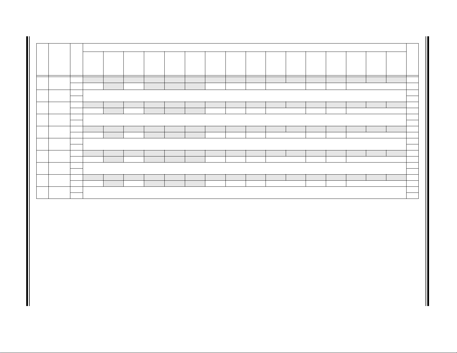
DS61168D-page 46 Preliminary © 2011-2012 Microchip Technology Inc.
TABLE 4-4: INPUT CAPTURE 1-INPUT CAPTURE 5 REGISTER MAP
PIC32MX1XX/2XX
Bits
Name
Register
(BF80_#)
Virtual Address
2000 IC1CON
2010 IC1BUF
2200 IC2CON
2210 IC2BUF
2400 IC3CON
2410 IC3BUF
2600 IC4CON
2610 IC4BUF
2800 IC5CON
2810 IC5BUF
Legend: x = unknown value on Reset; — = unimplemented, read as ‘0’. Reset values are shown in hexadecimal.
Note 1: This register has corresponding CLR, SET and INV registers at its virtual address, plus an offset of 0x4, 0x8 and 0xC, respectively. See Section 11.2 “CLR, SET and INV Registers” for more information.
(1)
(1)
(1)
(1)
(1)
31/15 30/14 29/13 28/12 27/11 26/10 25/9 24/8 23/7 22/6 21/5 20/4 19/3 18/2 17/1 16/0
Bit Range
31:16 — — — — — — — — — — — — — — — — 0000
15:0 ON
31:16
15:0 xxxx
31:16 — — — — — — — — — — — — — — — — 0000
15:0 ON
31:16
15:0 xxxx
31:16 — — — — — — — — — — — — — — — — 0000
15:0 ON
31:16
15:0 xxxx
31:16 — — — — — — — — — — — — — — — — 0000
15:0 ON
31:16
15:0 xxxx
31:16 — — — — — — — — — — — — — — — — 0000
15:0 ON
31:16
15:0 xxxx
—SIDL— — — FEDGE C32 ICTMR ICI<1:0> ICOV ICBNE ICM<2:0> 0000
IC1BUF<31:0>
—SIDL— — — FEDGE C32 ICTMR ICI<1:0> ICOV ICBNE ICM<2:0> 0000
IC2BUF<31:0>
—SIDL— — — FEDGE C32 ICTMR ICI<1:0> ICOV ICBNE ICM<2:0> 0000
IC3BUF<31:0>
—SIDL— — — FEDGE C32 ICTMR ICI<1:0> ICOV ICBNE ICM<2:0> 0000
IC4BUF<31:0>
—SIDL— — — FEDGE C32 ICTMR ICI<1:0> ICOV ICBNE ICM<2:0> 0000
IC5BUF<31:0>
xxxx
xxxx
xxxx
xxxx
xxxx
All Resets

© 2011-2012 Microchip Technology Inc. Preliminary DS61168D-page 47
TABLE 4-5: OUTPUT COMPARE 1-OUTPUT COMPARE 5 REGISTER MAP
(1)
Bits
Name
Register
(BF80_#)
Virtual Address
3000 OC1CON
3010 OC1R
3020 OC1RS
3200 OC2CON
3210 OC2R
3220 OC2RS
3400 OC3CON
3410 OC3R
3420 OC3RS
3600 OC4CON
3610 OC4R
3620 OC4RS
3800 OC5CON
3810 OC5R
3820 OC5RS
Legend: x = unknown value on Reset; — = unimplemented, read as ‘0’. Reset values are shown in hexadecimal.
Note 1: All registers in this table have corresponding CLR, SET and INV registers at their virtual addresses, plus offsets of 0x4, 0x8 and 0xC, respectively. See Section 11.2 “CLR, SET and INV Registers” for
more information.
31/15 30/14 29/13 28/12 27/11 26/10 25/9 24/8 23/7 22/6 21/5 20/4 19/3 18/2 17/1 16/0
Bit Range
31:16
15:0 ON
31:16
15:0 xxxx
31:16
15:0 xxxx
31:16
15:0 ON
31:16
15:0 xxxx
31:16
15:0 xxxx
31:16
15:0 ON
31:16
15:0 xxxx
31:16
15:0
31:16
15:0 ON
31:16
15:0 xxxx
31:16
15:0
31:16
15:0 ON
31:16
15:0 xxxx
31:16
15:0 xxxx
— — — — — — — — — — — — — — — — 0000
—SIDL— — — — — — — OC32 OCFLT OCTSEL OCM<2:0> 0000
OC1R<31:0>
OC1RS<31:0>
— — — — — — — — — — — — — — — — 0000
—SIDL— — — — — — — OC32 OCFLT OCTSEL OCM<2:0> 0000
OC2R<31:0>
OC2RS<31:0>
— — — — — — — — — — — — — — — — 0000
—SIDL— — — — — — — OC32 OCFLT OCTSEL OCM<2:0> 0000
OC3R<31:0>
OC3RS<31:0>
— — — — — — — — — — — — — — — — 0000
—SIDL— — — — — — — OC32 OCFLT OCTSEL OCM<2:0> 0000
OC4R<31:0>
OC4RS<31:0>
— — — — — — — — — — — — — — — — 0000
—SIDL— — — — — — — OC32 OCFLT OCTSEL OCM<2:0> 0000
OC5R<31:0>
OC5RS<31:0>
xxxx
xxxx
xxxx
xxxx
xxxx
xxxx
xxxx
xxxx
xxxx
xxxx
xxxx
xxxx
All Resets
PIC32MX1XX/2XX

DS61168D-page 48 Preliminary © 2011-2012 Microchip Technology Inc.
TABLE 4-6: I2C1 AND I2C2 REGISTER MAP
(1)
PIC32MX1XX/2XX
Bits
Name
Register
(BF80_#)
Virtual Address
5000 I2C1CON
5010 I2C1STAT
5020 I2C1ADD
5030 I2C1MSK
5040 I2C1BRG
5050 I2C1TRN
5060 I2C1RCV
5100 I2C2CON
5110 I2C2STAT
5120 I2C2ADD
5130 I2C2MSK
5140 I2C2BRG
5150 I2C2TRN
5160 I2C2RCV
Legend: x = unknown value on Reset; — = unimplemented, read as ‘0’. Reset values are shown in hexadecimal.
Note 1: All registers in this table except I2CxRCV have corresponding CLR, SET and INV registers at their virtual addresses, plus offsets of 0x4, 0x8 and 0xC, respectively. See Section 11.2 “CLR, SET and INV
Registers” for more information.
31/15 30/14 29/13 28/12 27/11 26/10 25/9 24/8 23/7 22/6 21/5 20/4 19/3 18/2 17/1 16/0
Bit Range
31:16
15:0 ON
31:16
15:0 ACKSTAT TRSTAT
31:16
15:0
31:16
15:0
31:16
15:0
31:16
15:0
31:16
15:0
31:16
15:0 ON
31:16
15:0 ACKSTAT TRSTAT
31:16
15:0
31:16
15:0
31:16
15:0
31:16
15:0
31:16
15:0
— — — — — — — — — — — — — — — — 0000
— SIDL SCLREL STRICT A10M DISSLW SMEN GCEN STREN ACKDT ACKEN RCEN PEN RSEN SEN 1000
— — — — — — — — — — — — — — — — 0000
— — — BCL GCSTAT ADD10 IWCOL I2COV D/A P S R/W RBF TBF 0000
— — — — — — — — — — — — — — — — 0000
— — — — — — Address Register 0000
— — — — — — — — — — — — — — — — 0000
— — — — — — Address Mask Register 0000
— — — — — — — — — — — — — — — — 0000
— — — — Baud Rate Generator Register 0000
— — — — — — — — — — — — — — — — 0000
— — — — — — — — Transmit Register 0000
— — — — — — — — — — — — — — — — 0000
— — — — — — — — Receive Register 0000
— — — — — — — — — — — — — — — — 0000
— SIDL SCLREL STRICT A10M DISSLW SMEN GCEN STREN ACKDT ACKEN RCEN PEN RSEN SEN 1000
— — — — — — — — — — — — — — — — 0000
— — — BCL GCSTAT ADD10 IWCOL I2COV D/A P S R/W RBF TBF 0000
— — — — — — — — — — — — — — — — 0000
— — — — — — Address Register 0000
— — — — — — — — — — — — — — — — 0000
— — — — — — Address Mask Register 0000
— — — — — — — — — — — — — — — — 0000
— — — — Baud Rate Generator Register 0000
— — — — — — — — — — — — — — — — 0000
— — — — — — — — Transmit Register 0000
— — — — — — — — — — — — — — — — 0000
— — — — — — — — Receive Register 0000
All Resets

© 2011-2012 Microchip Technology Inc. Preliminary DS61168D-page 49
TABLE 4-7: UART1 AND UART2 REGISTER MAP
Bits
Name
Register
(BF80_#)
Virtual Address
6000 U1MODE
6010 U1STA
6020 U1TXREG
6030 U1RXREG
6040 U1BRG
6200 U2MODE
6210 U2STA
6220 U2TXREG
6230 U2RXREG
6240 U2BRG
Legend: x = unknown value on Reset; — = unimplemented, read as ‘0’. Reset values are shown in hexadecimal.
Note 1: This register has corresponding CLR, SET and INV registers at its virtual address, plus an offset of 0x4, 0x8 and 0xC, respectively. See Section 11.2 “CLR, SET and INV Registers” for more information.
(1)
(1)
(1)
(1)
(1)
(1)
31/15 30/14 29/13 28/12 27/11 26/10 25/9 24/8 23/7 22/6 21/5 20/4 19/3 18/2 17/1 16/0
Bit Range
31:16 — — — — — — — — — — — — — — — — 0000
15:0 ON
31:16 — — — — — — — ADM_EN ADDR<7:0> 0000
15:0 UTXISEL<1:0> UTXINV URXEN UTXBRK UTXEN UTXBF TRMT URXISEL<1:0> ADDEN RIDLE PERR FERR OERR URXDA 0110
31:16
15:0
31:16
15:0
31:16 — — — — — — — — — — — — — — — — 0000
15:0 Baud Rate Generator Prescaler 0000
31:16
15:0
31:16 — — — — — — — ADM_EN ADDR<7:0> 0000
15:0 UTXISEL<1:0> UTXINV URXEN UTXBRK UTXEN UTXBF TRMT URXISEL<1:0> ADDEN RIDLE PERR FERR OERR URXDA 0110
31:16
15:0
31:16
15:0
31:16 — — — — — — — — — — — — — — — — 0000
15:0 Baud Rate Generator Prescaler 0000
— — — — — — — — — — — — — — — — 0000
— — — — — — — TX8 Transmit Register 0000
— — — — — — — — — — — — — — — — 0000
— — — — — — — RX8 Receive Register 0000
— — — — — — — — — — — — — — — — 0000
ON
— — — — — — — — — — — — — — — — 0000
— — — — — — — TX8 Transmit Register 0000
— — — — — — — — — — — — — — — — 0000
— — — — — — — RX8 Receive Register 0000
—SIDLIRENRTSMD— UEN<1:0> WAKE LPBACK ABAUD RXINV BRGH PDSEL<1:0> STSEL 0000
—SIDLIRENRTSMD— UEN<1:0> WAKE LPBACK ABAUD RXINV BRGH PDSEL<1:0> STSEL 0000
All Resets
PIC32MX1XX/2XX

DS61168D-page 50 Preliminary © 2011-2012 Microchip Technology Inc.
TABLE 4-8: SPI2 AND SPI2 REGISTER MAP
(1)
PIC32MX1XX/2XX
Bits
Name
Register
(BF80_#)
Virtual Address
5800 SPI1CON
SPI1STAT
5810
SPI1BUF
5820
SPI1BRG
5830
SPI1CON2
5840
SPI2CON
5A00
SPI2STAT
5A10
SPI2BUF
5A20
SPI2BRG
5A30
SPI2CON2
5A40
Legend: x = unknown value on Reset; — = unimplemented, read as ‘0’. Reset values are shown in hexadecimal.
Note 1: All registers in this table except SPIxBUF have corresponding CLR, SET and INV registers at their virtual addresses, plus offsets of 0x4, 0x8 and 0xC, respectively. See Section 11.2 “CLR, SET and INV
Registers” for more information.
31/15 30/14 29/13 28/12 27/11 26/10 25/9 24/8 23/7 22/6 21/5 20/4 19/3 18/2 17/1 16/0
Bit Range
31:16 FRMEN FRMSYNC FRMPOL MSSEN FRMSYPW FRMCNT<2:0> MCLKSEL
15:0 ON
31:16
15:0
31:16
15:0 0000
31:16
15:0
31:16
15:0
31:16 FRMEN FRMSYNC FRMPOL MSSEN FRMSYPW FRMCNT<2:0> MCLKSEL
15:0 ON
31:16
15:0
31:16
15:0 0000
31:16
15:0
31:16
15:0
— — — RXBUFELM<4:0> — — — TXBUFELM<4:0> 0000
— — — FRMERR SPIBUSY — — SPITUR SRMT SPIROV SPIRBE —SPITBE—SPITBFSPIRBF0008
— — — — — — — — — — — — — — — — 0000
— — — — — — —BRG<8:0>0000
— — — — — — — — — — — — — — — — 0000
SPI
SGNEXT
— — — RXBUFELM<4:0> — — — TXBUFELM<4:0> 0000
— — — FRMERR SPIBUSY — — SPITUR SRMT SPIROV SPIRBE —SPITBE—SPITBFSPIRBF0008
— — — — — — — — — — — — — — — — 0000
— — — — — — —BRG<8:0>0000
— — — — — — — — — — — — — — — — 0000
SPI
SGNEXT
— SIDL DISSDO MODE32 MODE16 SMP CKE SSEN CKP MSTEN DISSDI STXISEL<1:0> SRXISEL<1:0> 0000
DATA<31:0>
— —
— SIDL DISSDO MODE32 MODE16 SMP CKE SSEN CKP MSTEN DISSDI STXISEL<1:0> SRXISEL<1:0> 0000
— —
FRM
ERREN
FRM
ERREN
SPI
ROVEN
SPI
ROVEN
SPI
TUREN
SPI
TUREN
IGNROV IGNTUR AUDEN — — —
DATA<31:0>
IGNROV IGNTUR AUDEN — — —
— — — — — SPIFE ENHBUF 0000
0000
AUD-
MONO
— — — — — SPIFE ENHBUF 0000
AUD
MONO
— AUDMOD<1:0> 0000
0000
— AUDMOD<1:0> 0000
All Resets

© 2011-2012 Microchip Technology Inc. Preliminary DS61168D-page 51
TABLE 4-9: ADC REGISTER MAP
Bits
Register
Name
(BF80_#)
Virtual Address
9000 AD1CON1
9010 AD1CON2
9020 AD1CON3
9040 AD1CHS
9050 AD1CSSL
9070 ADC1BUF0
9080 ADC1BUF1
9090 ADC1BUF2
90A0 ADC1BUF3
90B0 ADC1BUF4
90C0 ADC1BUF5
90D0 ADC1BUF6
90E0 ADC1BUF7
90F0 ADC1BUF8
9100 ADC1BUF9
9110 ADC1BUFA
9120 ADC1BUFB
9130 ADC1BUFC
9140 ADC1BUFD
Legend: x = unknown value on Reset; — = unimplemented, read as ‘0’. Reset values are shown in hexadecimal.
Note 1: All registers in this table have corresponding CLR, SET and INV registers at their virtual addresses, plus offsets of 0x4, 0x8 and 0xC, respectively. See Section 11.2 “CLR, SET and INV Registers” for
(1)
(1)
(1)
(1)
(1)
details.
31/15 30/14 29/13 28/12 27/11 26/10 25/9 24/8 23/7 22/6 21/5 20/4 19/3 18/2 17/1 16/0
Bit Range
31:16 — — — — — — — — — — — — — — — — 0000
15:0 ON
31:16 — — — — — — — — — — — — — — — — 0000
15:0 VCFG<2:0> OFFCAL
31:16 — — — — — — — — — — — — — — — — 0000
15:0 ADRC
31:16 CH0NB — — — CH0SB<3:0> CH0NA — — — CH0SA<3:0> 0000
15:0
31:16 — — — — — — — — — — — — — — — — 0000
15:0 CSSL15 CSSL14 CSSL13 CSSL12 CSSL11 CSSL10 CSSL9 CSSL8 CSSL7 CSSL6 CSSL5 CSSL4 CSSL3 CSSL2 CSSL1 CSSL0 0000
31:16
15:0 0000
31:16
15:0 0000
31:16
15:0 0000
31:16
15:0 0000
31:16
15:0 0000
31:16
15:0 0000
31:16
15:0 0000
31:16
15:0 0000
31:16
15:0 0000
31:16
15:0 0000
31:16
15:0 0000
31:16
15:0 0000
31:16
15:0 0000
31:16
15:0 0000
— — — — — — — — — — — — — — — — 0000
—SIDL— — FORM<2:0> SSRC<2:0> CLRASAM —ASAMSAMPDONE0000
— CSCNA — —BUFS—SMPI<3:0>BUFMALTS0000
— — SAMC<4:0> ADCS<7:0> 0000
ADC Result Word 0 (ADC1BUF0<31:0>)
ADC Result Word 1 (ADC1BUF1<31:0>)
ADC Result Word 2 (ADC1BUF2<31:0>)
ADC Result Word 3 (ADC1BUF3<31:0>)
ADC Result Word 4 (ADC1BUF4<31:0>)
ADC Result Word 5 (ADC1BUF5<31:0>)
ADC Result Word 6 (ADC1BUF6<31:0>)
ADC Result Word 7 (ADC1BUF7<31:0>)
ADC Result Word 8 (ADC1BUF8<31:0>)
ADC Result Word 9 (ADC1BUF9<31:0>)
ADC Result Word A (ADC1BUFA<31:0>)
ADC Result Word B (ADC1BUFB<31:0>)
ADC Result Word C (ADC1BUFC<31:0>)
ADC Result Word D (ADC1BUFD<31:0>)
0000
0000
0000
0000
0000
0000
0000
0000
0000
0000
0000
0000
0000
0000
All Resets
PIC32MX1XX/2XX

DS61168D-page 52 Preliminary © 2011-2012 Microchip Technology Inc.
TABLE 4-9: ADC REGISTER MAP (CONTINUED)
Bits
Register
Name
(BF80_#)
Virtual Address
9150 ADC1BUFE
9160 ADC1BUFF
Legend: x = unknown value on Reset; — = unimplemented, read as ‘0’. Reset values are shown in hexadecimal.
Note 1: All registers in this table have corresponding CLR, SET and INV registers at their virtual addresses, plus offsets of 0x4, 0x8 and 0xC, respectively. See Section 11.2 “CLR, SET and INV Registers” for
details.
31/15 30/14 29/13 28/12 27/11 26/10 25/9 24/8 23/7 22/6 21/5 20/4 19/3 18/2 17/1 16/0
Bit Range
31:16
15:0 0000
31:16
15:0 0000
ADC Result Word E (ADC1BUFE<31:0>)
ADC Result Word F (ADC1BUFF<31:0>)
0000
0000
PIC32MX1XX/2XX
All Resets

© 2011-2012 Microchip Technology Inc. Preliminary DS61168D-page 53
TABLE 4-10: DMA GLOBAL REGISTER MAP
(1)
Bits
Name
Register
(BF88_#)
Virtual Address
3000 DMACON
3010 DMASTAT
3020 DMAADDR
Legend: x = unknown value on Reset; — = unimplemented, read as ‘0’. Reset values are shown in hexadecimal.
Note 1: All registers in this table have corresponding CLR, SET and INV registers at its virtual address, plus an offset of 0x4, 0x8 and 0xC, respectively. See Section 11.2 “CLR, SET and INV Registers” for more
information.
TABLE 4-11: DMA CRC REGISTER MAP
Name
Register
(BF88_#)
Virtual Address
3030 DCRCCON
3040 DCRCDATA
3050 DCRCXOR
Legend: x = unknown value on Reset; — = unimplemented, read as ‘0’. Reset values are shown in hexadecimal.
Note 1: All registers in this table have corresponding CLR, SET and INV registers at their virtual addresses, plus offsets of 0x4, 0x8 and 0xC, respectively. See Section 11.2 “CLR, SET and INV Registers” for
more information.
31/15 30/14 29/13 28/12 27/11 26/10 25/9 24/8 23/7 22/6 21/5 20/4 19/3 18/2 17/1 16/0
Bit Range
31:16
15:0 ON
31:16
15:0
31:16
15:0 0000
— — — — — — — — — — — — — — — — 0000
— — SUSPEND DMABUSY — — — — — — — — — — — 0000
— — — — — — — — — — — — — — — — 0000
— — — — — — — — — — — — RDWR DMACH<2:0>
DMAADDR<31:0>
(1)
31/15 30/14 29/13 28/12 27/11 26/10 25/9 24/8 23/7 22/6 21/5 20/4 19/3 18/2 17/1 16/0
Bit Range
31:16
15:0
31:16
15:0 0000
31:16
15:0 0000
— — BYTO<1:0> WBO — —BITO— — — — — — — — 0000
— — — PLEN<4:0> CRCEN CRCAPP CRCTYP — — CRCCH<2:0> 0000
Bits
DCRCDATA<31:0>
DCRCXOR<31:0>
(2)
0000
0000
0000
0000
All Resets
All Resets
PIC32MX1XX/2XX

DS61168D-page 54 Preliminary © 2011-2012 Microchip Technology Inc.
TABLE 4-12: DMA CHANNELS 0-3 REGISTER MAP
(1)
PIC32MX1XX/2XX
Bits
Name
Register
(BF88_#)
Virtual Address
3060 DCH0CON
3070 DCH0ECON
3080 DCH0INT
3090 DCH0SSA
30A0 DCH0DSA
30B0 DCH0SSIZ
30C0 DCH0DSIZ
30D0 DCH0SPTR
30E0 DCH0DPTR
30F0 DCH0CSIZ
3100 DCH0CPTR
3110 DCH0DAT
3120 DCH1CON
3130 DCH1ECON
3140 DCH1INT
3150 DCH1SSA
3160 DCH1DSA
Legend: x = unknown value on Reset; — = unimplemented, read as ‘0’. Reset values are shown in hexadecimal.
Note 1: All registers in this table have corresponding CLR, SET and INV registers at their virtual addresses, plus offsets of 0x4, 0x8 and 0xC, respectively. See Section 11.2 “CLR, SET and INV Registers” for
more information.
31/15 30/14 29/13 28/12 27/11 26/10 25/9 24/8 23/7 22/6 21/5 20/4 19/3 18/2 17/1 16/0
Bit Range
31:16
15:0 CHBUSY
31:16
15:0
31:16
15:0
31:16
15:0 0000
31:16
15:0 0000
31:16
15:0 CHSSIZ<15:0> 0000
31:16
15:0 CHDSIZ<15:0> 0000
31:16
15:0 CHSPTR<15:0> 0000
31:16
15:0 CHDPTR<15:0> 0000
31:16
15:0 CHCSIZ<15:0> 0000
31:16
15:0 CHCPTR<15:0> 0000
31:16
15:0
31:16
15:0 CHBUSY
31:16
15:0
31:16
15:0
31:16
15:0 0000
31:16
15:0 0000
— — — — — — — — — — — — — — — — 0000
— — — — — — CHCHNS CHEN CHAED CHCHN CHAEN — CHEDET CHPRI<1:0> 0000
— — — — — — — — CHAIRQ<7:0> 00FF
CHSIRQ<7:0> CFORCE CABORT PAT EN SIRQEN AIRQEN — — — FF00
— — — — — — — — CHSDIE CHSHIE CHDDIE CHDHIE CHBCIE CHCCIE CHTAIE CHERIE 0000
— — — — — — — — CHSDIF CHSHIF CHDDIF CHDHIF CHBCIF CHCCIF CHTAIF CHERIF 0000
CHSSA<31:0>
CHDSA<31:0>
— — — — — — — — — — — — — — — — 0000
— — — — — — — — — — — — — — — — 0000
— — — — — — — — — — — — — — — — 0000
— — — — — — — — — — — — — — — — 0000
— — — — — — — — — — — — — — — — 0000
— — — — — — — — — — — — — — — — 0000
— — — — — — — — — — — — — — — — 0000
— — — — — — — — CHPDAT<7:0> 0000
— — — — — — — — — — — — — — — — 0000
— — — — — — CHCHNS CHEN CHAED CHCHN CHAEN — CHEDET CHPRI<1:0> 0000
— — — — — — — — CHAIRQ<7:0> 00FF
CHSIRQ<7:0> CFORCE CABORT PAT EN SIRQEN AIRQEN — — — FF00
— — — — — — — — CHSDIE CHSHIE CHDDIE CHDHIE CHBCIE CHCCIE CHTAIE CHERIE 0000
— — — — — — — — CHSDIF CHSHIF CHDDIF CHDHIF CHBCIF CHCCIF CHTAIF CHERIF 0000
CHSSA<31:0>
CHDSA<31:0>
0000
0000
0000
0000
All Resets

© 2011-2012 Microchip Technology Inc. Preliminary DS61168D-page 55
TABLE 4-12: DMA CHANNELS 0-3 REGISTER MAP
(1)
(CONTINUED)
Bits
Name
Register
(BF88_#)
Virtual Address
3170 DCH1SSIZ
3180 DCH1DSIZ
3190 DCH1SPTR
31A0 DCH1DPTR
31B0 DCH1CSIZ
31C0 DCH1CPTR
31D0 DCH1DAT
31E0 DCH2CON
31F0 DCH2ECON
3200 DCH2INT
3210 DCH2SSA
3220 DCH2DSA
3230 DCH2SSIZ
3240 DCH2DSIZ
3250 DCH2SPTR
3260 DCH2DPTR
3270 DCH2CSIZ
Legend: x = unknown value on Reset; — = unimplemented, read as ‘0’. Reset values are shown in hexadecimal.
Note 1: All registers in this table have corresponding CLR, SET and INV registers at their virtual addresses, plus offsets of 0x4, 0x8 and 0xC, respectively. See Section 11.2 “CLR, SET and INV Registers” for
more information.
31/15 30/14 29/13 28/12 27/11 26/10 25/9 24/8 23/7 22/6 21/5 20/4 19/3 18/2 17/1 16/0
Bit Range
31:16
15:0 CHSSIZ<15:0> 0000
31:16
15:0 CHDSIZ<15:0> 0000
31:16
15:0 CHSPTR<15:0> 0000
31:16
15:0 CHDPTR<15:0> 0000
31:16
15:0 CHCSIZ<15:0> 0000
31:16
15:0 CHCPTR<15:0> 0000
31:16
15:0
31:16
15:0 CHBUSY
31:16
15:0
31:16
15:0
31:16
15:0 0000
31:16
15:0 0000
31:16
15:0 CHSSIZ<15:0> 0000
31:16
15:0 CHDSIZ<15:0> 0000
31:16
15:0 CHSPTR<15:0> 0000
31:16
15:0 CHDPTR<15:0> 0000
31:16
15:0 CHCSIZ<15:0> 0000
— — — — — — — — — — — — — — — — 0000
— — — — — — — — — — — — — — — — 0000
— — — — — — — — — — — — — — — — 0000
— — — — — — — — — — — — — — — — 0000
— — — — — — — — — — — — — — — — 0000
— — — — — — — — — — — — — — — — 0000
— — — — — — — — — — — — — — — — 0000
— — — — — — — — CHPDAT<7:0> 0000
— — — — — — — — — — — — — — — — 0000
— — — — — — CHCHNS CHEN CHAED CHCHN CHAEN — CHEDET CHPRI<1:0> 0000
— — — — — — — — CHAIRQ<7:0> 00FF
CHSIRQ<7:0> CFORCE CABORT PAT EN SIRQEN AIRQEN — — — FF00
— — — — — — — — CHSDIE CHSHIE CHDDIE CHDHIE CHBCIE CHCCIE CHTAIE CHERIE 0000
— — — — — — — — CHSDIF CHSHIF CHDDIF CHDHIF CHBCIF CHCCIF CHTAIF CHERIF 0000
CHSSA<31:0>
CHDSA<31:0>
— — — — — — — — — — — — — — — — 0000
— — — — — — — — — — — — — — — — 0000
— — — — — — — — — — — — — — — — 0000
— — — — — — — — — — — — — — — — 0000
— — — — — — — — — — — — — — — — 0000
0000
0000
All Resets
PIC32MX1XX/2XX

DS61168D-page 56 Preliminary © 2011-2012 Microchip Technology Inc.
TABLE 4-12: DMA CHANNELS 0-3 REGISTER MAP
(1)
(CONTINUED)
PIC32MX1XX/2XX
Bits
Name
Register
(BF88_#)
Virtual Address
3280 DCH2CPTR
3290 DCH2DAT
32A0 DCH3CON
32B0 DCH3ECON
32C0 DCH3INT
32D0 DCH3SSA
32E0 DCH3DSA
32F0 DCH3SSIZ
3300 DCH3DSIZ
3310 DCH3SPTR
3320 DCH3DPTR
3330 DCH3CSIZ
3340 DCH3CPTR
3350 DCH3DAT
Legend: x = unknown value on Reset; — = unimplemented, read as ‘0’. Reset values are shown in hexadecimal.
Note 1: All registers in this table have corresponding CLR, SET and INV registers at their virtual addresses, plus offsets of 0x4, 0x8 and 0xC, respectively. See Section 11.2 “CLR, SET and INV Registers” for
more information.
31/15 30/14 29/13 28/12 27/11 26/10 25/9 24/8 23/7 22/6 21/5 20/4 19/3 18/2 17/1 16/0
Bit Range
31:16
15:0 CHCPTR<15:0> 0000
31:16
15:0
31:16
15:0 CHBUSY
31:16
15:0
31:16
15:0
31:16
15:0 0000
31:16
15:0 0000
31:16
15:0 CHSSIZ<15:0> 0000
31:16
15:0 CHDSIZ<15:0> 0000
31:16
15:0 CHSPTR<15:0> 0000
31:16
15:0 CHDPTR<15:0> 0000
31:16
15:0 CHCSIZ<15:0> 0000
31:16
15:0 CHCPTR<15:0> 0000
31:16
15:0
— — — — — — — — — — — — — — — — 0000
— — — — — — — — — — — — — — — — 0000
— — — — — — — — CHPDAT<7:0> 0000
— — — — — — — — — — — — — — — — 0000
— — — — — — CHCHNS CHEN CHAED CHCHN CHAEN — CHEDET CHPRI<1:0> 0000
— — — — — — — — CHAIRQ<7:0> 00FF
CHSIRQ<7:0> CFORCE CABORT PAT EN SIRQEN AIRQEN — — — FF00
— — — — — — — — CHSDIE CHSHIE CHDDIE CHDHIE CHBCIE CHCCIE CHTAIE CHERIE 0000
— — — — — — — — CHSDIF CHSHIF CHDDIF CHDHIF CHBCIF CHCCIF CHTAIF CHERIF 0000
CHSSA<31:0>
CHDSA<31:0>
— — — — — — — — — — — — — — — — 0000
— — — — — — — — — — — — — — — — 0000
— — — — — — — — — — — — — — — — 0000
— — — — — — — — — — — — — — — — 0000
— — — — — — — — — — — — — — — — 0000
— — — — — — — — — — — — — — — — 0000
— — — — — — — — — — — — — — — — 0000
— — — — — — — — CHPDAT<7:0> 0000
0000
0000
All Resets

© 2011-2012 Microchip Technology Inc. Preliminary DS61168D-page 57
TABLE 4-13: COMPARATOR REGISTER MAP
(1)
Bits
Name
Register
(BF80_#)
Virtual Address
A000 CM1CON
A010 CM2CON
A020 CM3CON
A060 CMSTAT
Legend: x = unknown value on Reset; — = unimplemented, read as ‘0’. Reset values are shown in hexadecimal.
Note 1: All registers in this table have corresponding CLR, SET and INV registers at their virtual addresses, plus offsets of 0x4, 0x8 and 0xC, respectively. See Section 11.2 “CLR, SET and INV Registers” for
more information.
31/15 30/14 29/13 28/12 27/11 26/10 25/9 24/8 23/7 22/6 21/5 20/4 19/3 18/2 17/1 16/0
Bit Range
31:16
15:0 ON COE CPOL
31:16
15:0 ON COE CPOL
31:16
15:0 ON COE CPOL
31:16
15:0
— — — — — — — — — — — — — — — — 0000
— — — —COUT EVPOL<1:0> — CREF — — CCH<1:0> 00C3
— — — — — — — — — — — — — — — — 0000
— — — —COUT EVPOL<1:0> — CREF — — CCH<1:0> 00C3
— — — — — — — — — — — — — — — — 0000
— — — —COUT EVPOL<1:0> — CREF — — CCH<1:0> 00C3
— — — — — — — — — — — — — — — — 0000
— —SIDL— — — — — — — — — — C3OUT C2OUT C1OUT 0000
TABLE 4-14: COMPARATOR VOLTAGE REFERENCE REGISTER MAP
Name
Register
(BF80_#)
Virtual Address
9800 CVRCON
Legend: x = unknown value on Reset; — = unimplemented, read as ‘0’. Reset values are shown in hexadecimal.
Note 1: All registers in this table have corresponding CLR, SET and INV registers at their virtual addresses, plus offsets of 0x4, 0x8 and 0xC, respectively. See Section 11.2 “CLR, SET and INV Registers” for
more information.
31/15 30/14 29/13 28/12 27/11 26/10 25/9 24/8 23/7 22/6 21/5 20/4 19/3 18/2 17/1 16/0
Bit Range
31:16
15:0 ON
— — — — — — — — — — — — — — — — 0000
— — — — — — — — CVROE CVRR CVRSS CVR<3:0> 0000
(1)
Bits
All Resets
All Resets
PIC32MX1XX/2XX

DS61168D-page 58 Preliminary © 2011-2012 Microchip Technology Inc.
TABLE 4-15: FLASH CONTROLLER REGISTER MAP
PIC32MX1XX/2XX
Bits
Name
Register
(BF80_#)
Virtual Address
F400 NVMCON
F410 NVMKEY
F420
NVMADDR
F430 NVMDATA
F440
Legend: x = unknown value on Reset; — = unimplemented, read as ‘0’. Reset values are shown in hexadecimal.
Note 1: This register has corresponding CLR, SET and INV registers at their virtual addresses, plus offsets of 0x4, 0x8 and 0xC, respectively. See Section 11.2 “CLR, SET and INV Registers” for more
(1)
(1)
NVMSRC
ADDR
information.
31/15 30/14 29/13 28/12 27/11 26/10 25/9 24/8 23/7 22/6 21/5 20/4 19/3 18/2 17/1 16/0
Bit Range
31:16 — — — — — — — — — — — — — — — — 0000
15:0 WR WREN WRERR LVDERR LVDSTAT
31:16
15:0 0000
31:16
15:0 0000
31:16
15:0 0000
31:16
15:0 0000
— — — — — — — NVMOP<3:0> 0000
NVMKEY<31:0>
NVMADDR<31:0>
NVMDATA<31:0>
NVMSRCADDR<31:0>
All Resets
0000
0000
0000
0000

© 2011-2012 Microchip Technology Inc. Preliminary DS61168D-page 59
TABLE 4-16: SYSTEM CONTROL REGISTER MAP
(1)
Bits
Name
Register
(BF80_#)
Virtual Address
OSCCON
F000
F010 OSCTUN
REFOCON
F020
REFOTRIM
F030
0000 WDTCON
F600 RCON
F610 RSWRST
CFGCON
F200
(3)
SYSKEY
F230
PMD1
F240
PMD2
F250
PMD3
F260
PMD4
F270
PMD5
F280
PMD6
F290
Legend: x = unknown value on Reset; — = unimplemented, read as ‘0’. Reset values are shown in hexadecimal.
Note 1: With the exception of those noted, all registers in this table have corresponding CLR, SET and INV registers at their virtual addresses, plus offsets of 0x4, 0x8 and 0xC, respectively. See Section 11.2
“CLR, SET and INV Registers” for more information.
2: Reset values are dependent on the DEVCFGx Configuration bits and the type of reset.
3: This register does not have associated CLR, SET, INV registers.
4: This bit is available on PIC32MX2XX devices only.
31/15 30/14 29/13 28/12 27/11 26/10 25/9 24/8 23/7 22/6 21/5 20/4 19/3 18/2 17/1 16/0
Bit Range
31:16
31:16
31:16
31:16 ROTRIM<8:0>
31:16
31:16
31:16
31:16
31:16
31:16
31:16
31:16
31:16
31:16
31:16
— — PLLODIV<2:0> FRCDIV<2:0> — SOSCRDY PBDIVRDY PBDIV<1:0> PLLMULT<2:0> x1xx
15:0 — COSC<2:0> — NOSC<2:0> CLKLOCK ULOCK
— — — — — — — — — — — — — — — — 0000
15:0
— — — — — — — — — —TUN<5:0>0000
— RODIV<14:0> 0000
15:0 ON
15:0
— — — — — — — —
— — — — — — — — — — — — — — — — 0000
15:0 ON
— — — — — — — — — — — — — — — — 0000
15:0
— — — — — — CMR VREGS EXTR SWR — WDTO SLEEP IDLE BOR POR xxxx
— — — — — — — — — — — — — — — — 0000
15:0
— — — — — — — — — — — — — — —SWRST0000
— — — — — — — — — — — — — — — — 0000
— —IOLOCKPMDLOCK— — — — — — — —JTAGEN
15:0
15:0 0000
— — — — — — — — — — — — — — — — 0000
15:0
— — —CVRMD— — —CTMUMD— — — — — — —AD1MD0000
— — — — — — — — — — — — — — — — 0000
15:0
— — — — — — — — — — — — — CMP3MD CMP2MD CMP1MD 0000
— — — — — — — — — — — OC5MD OC4MD OC3MD OC2MD OC1MD 0000
15:0
— — — — — — — — — — — IC5MD IC4MD IC3MD IC2MD IC1MD 0000
— — — — — — — — — — — — — — — — 0000
15:0
— — — — — — — — — — — T5MD T4MD T3MD T2MD T1MD 0000
— — — — — — — USB1MD — — — — — — I2C1MD I2C1MD 0000
15:0
— — — — — — SPI2MD SPI1MD — — — — — —U2MDU1MD0000
— — — — — — — — — — — — — — — PMPMD 0000
15:0
— — — — — — — — — — — — — —REFOMDRTCCMD0000
—SIDL OERSLP— DIVSWEN ACTIVE — — — —
—
— — — — — — — — SWDTPS<4:0> WDTWINEN WDTCLR 0000
SYSKEY<31:0>
(4)
SLOCK SLPEN CF UFRCEN
— — — — — — —
— — — — — — —
(4)
SOSCEN OSWEN xxxx
ROSEL<3:0>
— —
TDOEN 000B
0000
0000
0000
0000
All Resets
(2)
(2)
(2)
PIC32MX1XX/2XX

DS61168D-page 60 Preliminary © 2011-2012 Microchip Technology Inc.
TABLE 4-17: DEVCFG: DEVICE CONFIGURATION WORD SUMMARY
PIC32MX1XX/2XX
Bits
Name
Register
(BFC0_#)
Virtual Address
2FF0 DEVCFG3
2FF4 DEVCFG2
2FF8 DEVCFG1
2FFC DEVCFG0
Legend: x = unknown value on Reset; — = unimplemented, read as ‘0’. Reset values are shown in hexadecimal.
Note 1: This bit is available on PIC32MX2XX devices only.
31:16 FVBUSONID FUSBIDIO IOL1WAY PMDL1WAY
31:16
31:16
31:16
TABLE 4-18: DEVICE AND REVISION ID SUMMARY
Name
Register
(BF80_#)
Virtual Address
F220 DEVID
Legend: x = unknown value on Reset; — = unimplemented, read as ‘0’. Reset values are shown in hexadecimal.
Note 1: Reset values are dependent on the device variant.
31/15 30/14 29/13 28/12 27/11 26/10 25/9 24/8 23/7 22/6 21/5 20/4 19/3 18/2 17/1 16/0
Bit Range
—
15:0 USERID<15:0> xxxx
— — — — — — — — — — — — — FPLLODIV<2:0> xxxx
15:0
15:0 FCKSM<1:0> FPBDIV<1:0>
15:0 PWP<5:0>
(1)
UPLLEN
— — — — — — FWDTWINSZ<1:0> FWDTEN WINDIS —WDTPS<4:0>xxxx
— — —CP— — —BWP— — — — — — — — xxxx
— — — — UPLLIDIV<2:0>
— OSCIOFNC POSCMOD<1:0> IESO — FSOSCEN — —FNOSC<2:0>xxxx
— — —
(1)
— — — — — ICESEL<1:0> JTAGEN DEBUG<1:0> xxxx
(1)
Bits
31/15 30/14 29/13 28/12 27/11 26/10 25/9 24/8 23/7 22/6 21/5 20/4 19/3 18/2 17/1 16/0
Bit Range
31:16 VER<3:0> DEVID<27:16> xxxx
15:0 DEVID<15:0> xxxx
All Resets
— — — — — — — — xxxx
—FPLLMUL<2:0>— FPLLIDIV<2:0> xxxx
All Resets

© 2011-2012 Microchip Technology Inc. Preliminary DS61168D-page 61
TABLE 4-19: PORTA REGISTER MAP
(1)
Bits
Name
Register
(BF88_#)
31/15 30/14 29/13 28/12 27/11 26/10 25/9 24/8 23/7 22/6 21/5 20/4 19/3 18/2 17/1 16/0
Bit Range
Virtual Address
6000 ANSELA
6010 TRISA
6020 PORTA
6030 LATA
6040 ODCA
6050 CNPUA
6060 CNPDA
6070 CNCONA
6080 CNENA
60 90 C NSTATA
— — — — — — — — — — — — — —
31:16
— — — — — — — — — — — — — — ANSA1 ANSA0 0003
15:0
31:16
— — — — — — — — — — — — — — — — 0000
15:0
— — — — —TRISA10
31:16
— — — — — — — — — — — 0000
15:0
— — — — —RA10
31:16
— — — — — — — — — — — — — — — — 0000
15:0
— — — — —LATA10
31:16
— — — — — — — — — — — — — — — — 0000
15:0
— — — — — ODCA10
31:16
— — — — — — — — — — — — — — — — 0000
15:0
— — — — — CNPUA10
31:16
— — — — — — — — — — — — — — — — 0000
15:0
— — — — — CNPDA10
31:16
— — — — — — — — — — — — — — — — 0000
15:0 ON
31:16
— — — — — — — — — — — — — — — — 0000
15:0
— — — — — CNIEA10
31:16
— — — — — — — — — — — — — — — — 0000
15:0
— — — — — CNSTATA10
—SIDL— — — — — — — — — — — — — 0000
(2)
(2)
(2)
(2)
(2)
(2)
(2)
TRISA9
LATA9
ODCA9
CNPUA9
CNPDA9
CNIEA9
(2)
CNSTATA9
RA9
(2)
(2)
(2)
(2)
(2)
(2)
(2)
(2)
CN STATA 8
TRISA8
RA8
LATA8
ODCA8
CNPUA8
CNPDA8
CNIEA8
(2)
(2)
(2)
(2)
(2)
(2)
(2)
TRISA7
LATA7
ODCA7
CNPUA7
CNPDA7
CNIEA7
(2)
CNSTATA7
RA7
(2)
— — TRISA4 TRISA3 TRISA2 TRISA1 TRISA0 079F
(2)
— — RA4 RA3 RA2 RA1 RA0 xxxx
(2)
— — L ATA4 L ATA3 LATA 2 LATA 1 L ATA0 xxxx
(2)
— — — — — — — 0000
(2)
— — CNPUA4 CNPUA3 CNPUA2 CNPUA1 CNPUA0 0000
(2)
— — CNPDA4 CNPDA3 CNPDA2 CNPDA1 CNPDA0 0000
(2)
— — CNIEA4 CNIEA3 CNIEA2 CNIEA1 CNIEA0 0000
(2)
— — CNSTATA4 CNSTATA3CNSTATA2 CNSTATA1CNSTATA0 0000
— —
0000
Legend: x = unknown value on Reset; — = unimplemented, read as ‘0’. Reset values are shown in hexadecimal.
Note 1: All registers in this table have corresponding CLR, SET and INV registers at their virtual addresses, plus offsets of 0x4, 0x8 and 0xC, respectively. See Section 11.2 “CLR, SET and INV Registers” for
more information.
2: This bit is available on 44-pin devices only.
All Resets
PIC32MX1XX/2XX

DS61168D-page 62 Preliminary © 2011-2012 Microchip Technology Inc.
TABLE 4-20: PORTB REGISTER MAP
PIC32MX1XX/2XX
Bits
Name
Register
(BF88_#)
31/15 30/14 29/13 28/12 27/11 26/10 25/9 24/8 23/7 22/6 21/5 20/4 19/3 18/2 17/1 16/0
Bit Range
Virtual Address
6100 ANSELB
6110 TRISB
6120 PORTB
6130 LATB
6140 ODCB
6150 CNPUB
6160 CNPDB
6170 CNCONB
6180 CNENB
6190 CNSTATB
31:16
— — — — — — — — — — — — — —
15:0 ANSB15 ANSB14 ANSB13 ANSB12
31:16
— — — — — — — — — — — — — — — — 0000
15:0 TRISB15 TRISB14 TRISB13 TRISB12
31:16
— — — — — — — — — — — 0000
15:0 RB15 RB14 RB13 RB12
31:16
— — — — — — — — — — — — — — — — 0000
15 :0 L ATB1 5 LAT B14 L ATB 13 LATB 12
31:16
15:0
31:16
— — — — — — — — — — — — — — — — 0000
— — — — ODCB11 ODCB10 ODCB9 ODCB8 ODCB7 ODCB6 ODCB5 ODCB4 — — — — 0000
— — — — — — — — — — — — — — — — 0000
15:0 CNPUB15 CNPUB14 CNPUB13 CNPUB12
31:16
— — — — — — — — — — — — — — — — 0000
15:0 CNPDB15 CNPDB14 CNPDB13 CNPDB12
31:16
15:0 ON
31:16
— — — — — — — — — — — — — — — — 0000
—SIDL — — — — — — — — — — — — — 0000
— — — — — — — — — — — — — — — — 0000
15:0 CNIEB15 CNIEB14 CNIEB13 CNIEB11
31:16
15:0
— — — — — — — — — — — — — — — — 0000
CN
STATB15CNSTATB14CNSTATB13CNSTATB12
(2)
— — — — — — — — ANSB3 ANSB2 ANSB1 ANSB0 E00F
(2)
TRISB11 TRISB10 TRISB9 TRISB8 TRISB7 TRISB6
(2)
RB11 RB10 RB9 RB8 RB7 RC6
(2)
LATB11 LATB10 LATB9 LATB8 LATB7 LATB6
(2)
CNPUB11 CNPUB10 CNPUB9 CNPUB8 CNPUB7 CNPUB6
(2)
CNPDB11 CNPDB10 CNPDB9 CNPDB8 CNPDB7 CNPDB6
(2)
CNIEB11 CNIEB10 CNIEB9 CNIEB8 CNIEB7 CNIEB6
CN
(2)
STATB11CNSTATB10CNSTATB9CNSTATB8CNSTATB7CNSTATB6
(2)
TRISB5 TRISB4 TRISB3 TRISB2 TRISB1 TRISB0 FFFF
(2)
RB5 RB4 RB3 RB2 RB1 RB0 xxxx
(2)
LATB5 LATB4 LATB3 LATB2 LATB1 LATB0 xxxx
(2)
CNPUB5 CNPUB4 CNPUB3 CNPUB2 CNPUB1 CNPUB0 0000
(2)
CNPDB5 CNPDB4 CNPDB3 CNPDB2 CNPDB1 CNPDB0 0000
(2)
CNIEB5 CNIEB4 CNIEB3 CNIEB2 CNIEB1 CNIEB0 0000
CN
(2)
STATB5CNSTATB4CNSTATB3CNSTATB2CNSTATB1CNSTATB0
— —
0000
0000
Legend: x = unknown value on Reset; — = unimplemented, read as ‘0’. Reset values are shown in hexadecimal.
Note 1: All registers in this table have corresponding CLR, SET and INV registers at their virtual addresses, plus offsets of 0x4, 0x8 and 0xC, respectively. See Section 11.2 “CLR, SET and INV Registers” for
more information.
2: This bit is not available on PIC32MX2XX devices. The reset value for the TRISB register when this bit is not available is 0x0000EFBF.
All Resets

© 2011-2012 Microchip Technology Inc. Preliminary DS61168D-page 63
TABLE 4-21: PORTC REGISTER MAP
(1,2)
Bits
Name
Register
(BF88_#)
31/15 30/14 29/13 28/12 27/11 26/10 25/9 24/8 23/7 22/6 21/5 20/4 19/3 18/2 17/1 16/0
Bit Range
Virtual Address
6200 ANSELC
6210 TRISC
6220 PORTC
6230 LATC
6240 ODCC
6250 CNPUC
6260 CNPDC
6270 CNCONC
6280 CNENC
6290 CNSTATC
— — — — — — — — — — — — — —
31:16
— — — — — — — — — — — — ANSC3 ANSC2
15:0
31:16
— — — — — — — — — — — — — — — — 0000
15:0
— — — — — — TRISC9 TRISC8
31:16
— — — — — — — — — — — 0000
15:0
— — — — — — RC9 RC8
31:16
— — — — — — — — — — — — — — — — 0000
15:0
— — — — — —LATC9LATC8
31:16
— — — — — — — — — — — — — — — — 0000
15:0
— — — — — — ODCC9 ODCC8
31:16
— — — — — — — — — — — — — — — — 0000
15:0
— — — — — — CNPUC9 CNPUC8
31:16
— — — — — — — — — — — — — — — — 0000
15:0
— — — — — — CNPDC9 CNPDC8
31:16
— — — — — — — — — — — — — — — — 0000
15:0 ON
31:16
15:0
31:16
15:0
—SIDL— — — — — — — — — — — — — 0000
— — — — — — — — — — — — — — — — 0000
— — — — — — CNIEC9 CNIEC8
— — — — — — — — — — — — — — — — 0000
— — — — — — CNSTATC9 CNSTATC8
(3)
(3)
(3)
(3)
(3)
(3)
(3)
TRISC7
RC7
LATC7
ODCC7
CNPUC7
CNPDC7
CNIEC7
(3)
CNSTATC7
(3)
(3)
(3)
(3)
(3)
(3)
(3)
TRISC6
RC6
LATC6
ODCC6
CNPUC6
CNPDC6
CNIEC6
(3)
CNSTATC6
(3)
(3)
(3)
(3)
(3)
(3)
(3)
TRISC5
RC5
LATC5
ODCC5
CNPUC5
CNPDC5
CNIEC5
(3)
CNSTATC5
(3)
(3)
(3)
(3)
(3)
(3)
(3)
TRISC4
RC4
LATC4
ODCC4
CNPUC4
CNPDC4
CNIEC4
(3)
CNSTATC4
(3)
TRISC3 TRISC2
(3)
RC3 RC2
(3)
LATC3 LATC2
(3)
— — — — 0000
(3)
CNPUC3 CNPUC2
(3)
CNPDC3 CNPDC2
(3)
CNIEC3 CNIEC2
(3)
CNSTATC3 CNSTATC2
(3)
— —
(3)
ANSC1 ANSC0 000F
(3)
TRISC1 TRISC0 03FF
RC1 RC0 xxxx
(3)
LATC1 LATC0 xxxx
(3)
CNPUC1 CNPUC0 0000
(3)
CNPDC1 CNPDC0 0000
(3)
CNIEC1 CNIEC0 0000
(3)
CNSTATC1 CNSTATC0 0000
0000
Legend: x = unknown value on Reset; — = unimplemented, read as ‘0’. Reset values are shown in hexadecimal.
Note 1: All registers in this table have corresponding CLR, SET and INV registers at their virtual addresses, plus offsets of 0x4, 0x8 and 0xC, respectively. See Section 11.2 “CLR, SET and INV Registers” for
more information.
2: PORTC is not available on 28-pin devices.
3: This bit is available on 44-pin devices only.
All Resets
PIC32MX1XX/2XX

DS61168D-page 64 Preliminary © 2011-2012 Microchip Technology Inc.
TABLE 4-22: PERIPHERAL PIN SELECT INPUT REGISTER MAP
PIC32MX1XX/2XX
Bits
Register
(BF80_#)
Virtual Address
FA04 IN T1R
FA08 IN T2R
FA0C INT3R
FA10 IN T4R
FA18 T2CKR
FA1C T 3CKR
FA20 T4CKR
FA24 T5CKR
FA28 IC1R
FA2C IC2R
FA30 IC3R
FA34 IC4R
FA38 IC5R
FA48 O CFA R
FA4C OCF BR
FA50 U1RXR
Name
31/15 30/14 29/13 28/12 27/11 26/10 25/9 24/8 23/7 22/6 21/5 20/4 19/3 18/2 17/1 16/0
Bit Range
31:16
15:0
31:16
15:0
31:16
15:0
31:16
15:0
31:16
15:0
31:16
15:0
31:16
15:0
31:16
15:0
31:16
15:0
31:16
15:0
31:16
15:0
31:16
15:0
31:16
15:0
31:16
15:0
31:16
15:0
31:16
15:0
— — — — — — — — — — — — — — — — 0000
— — — — — — — — — — — —INT1R<3:0>0000
— — — — — — — — — — — — — — — — 0000
— — — — — — — — — — — —INT2R<3:0>0000
— — — — — — — — — — — — — — — — 0000
— — — — — — — — — — — —INT3R<3:0>0000
— — — — — — — — — — — — — — — — 0000
— — — — — — — — — — — —INT4R<3:0>0000
— — — — — — — — — — — — — — — — 0000
— — — — — — — — — — — —T2CKR<3:0>0000
— — — — — — — — — — — — — — — — 0000
— — — — — — — — — — — —T3CKR<3:0>0000
— — — — — — — — — — — — — — — — 0000
— — — — — — — — — — — —T4CKR<3:0>0000
— — — — — — — — — — — — — — — — 0000
— — — — — — — — — — — —T5CKR<3:0>0000
— — — — — — — — — — — — — — — — 0000
— — — — — — — — — — — —IC1R<3:0>0000
— — — — — — — — — — — — — — — — 0000
— — — — — — — — — — — —IC2R<3:0>0000
— — — — — — — — — — — — — — — — 0000
— — — — — — — — — — — —IC3R<3:0>0000
— — — — — — — — — — — — — — — — 0000
— — — — — — — — — — — —IC4R<3:0>0000
— — — — — — — — — — — — — — — — 0000
— — — — — — — — — — — —IC5R<3:0>0000
— — — — — — — — — — — — — — — — 0000
— — — — — — — — — — — —OCFAR<3:0>0000
— — — — — — — — — — — — — — — — 0000
— — — — — — — — — — — —OCFBR<3:0>0000
— — — — — — — — — — — — — — — — 0000
— — — — — — — — — — — —U1RXR<3:0>0000
All Resets

© 2011-2012 Microchip Technology Inc. Preliminary DS61168D-page 65
TABLE 4-22: PERIPHERAL PIN SELECT INPUT REGISTER MAP (CONTINUED)
Bits
Name
Register
(BF80_#)
Virtual Address
FA54 U1CTSR
FA58 U2RXR
FA5C U2CTSR
FA84 SDI1R
FA88 SS1R
FA90 SDI2R
FA94 SS2R
FAB8 REFC LK IR
31/15 30/14 29/13 28/12 27/11 26/10 25/9 24/8 23/7 22/6 21/5 20/4 19/3 18/2 17/1 16/0
Bit Range
31:16
15:0
31:16
15:0
31:16
15:0
31:16
15:0
31:16
15:0
31:16
15:0
31:16
15:0
31:16
15:0
— — — — — — — — — — — — — — — — 0000
— — — — — — — — — — — — U1CTSR<3:0> 0000
— — — — — — — — — — — — — — — — 0000
— — — — — — — — — — — —U2RXR<3:0>0000
— — — — — — — — — — — — — — — — 0000
— — — — — — — — — — — — U2CTSR<3:0> 0000
— — — — — — — — — — — — — — — — 0000
— — — — — — — — — — — —SDI1R<3:0>0000
— — — — — — — — — — — — — — — — 0000
— — — — — — — — — — — — SS1R<3:0> 0000
— — — — — — — — — — — — — — — — 0000
— — — — — — — — — — — —SDI2R<3:0>0000
— — — — — — — — — — — — — — — — 0000
— — — — — — — — — — — — SS2R<3:0> 0000
— — — — — — — — — — — — — — — — 0000
— — — — — — — — — — — — REFCLKIR<3:0> 0000
All Resets
PIC32MX1XX/2XX

DS61168D-page 66 Preliminary © 2011-2012 Microchip Technology Inc.
TABLE 4-23: PERIPHERAL PIN SELECT OUTPUT REGISTER MAP
PIC32MX1XX/2XX
Bits
Name
Register
(BF80_#)
Virtual Address
FB00 RPA0R
FB04 RPA1R
FB08 RPA2R
FB0C RPA3R
FB10 RPA4R
FB20 RPA8R
FB24 RPA9R
FB2C RPB0R
FB30 RPB1R
FB34 RPB2R
FB38 RPB3R
FB3C RPB4R
FB40 RPB5R
FB44 RPB6R
FB48 RPB7R
FB4C RPB8R
Note 1: This register is only available on 44-pin devices.
(1)
(1)
(2)
2: This register is only available on PIC32MX1XX devices.
3: This register is only available on 36-pin and 44-pin devices.
31/15 30/14 29/13 28/12 27/11 26/10 25/9 24/8 23/7 22/6 21/5 20/4 19/3 18/2 17/1 16/0
Bit Range
31:16
15:0
31:16
15:0
31:16
15:0
31:16
15:0
31:16
15:0
31:16
15:0
31:16
15:0
31:16
15:0
31:16
15:0
31:16
15:0
31:16
15:0
31:16
15:0
31:16
15:0
31:16
15:0
31:16
15:0
31:16
15:0
— — — — — — — — — — — — — — — — 0000
— — — — — — — — — — — — RPA0<3:0> 0000
— — — — — — — — — — — — — — — — 0000
— — — — — — — — — — — — RPA1<3:0> 0000
— — — — — — — — — — — — — — — — 0000
— — — — — — — — — — — — RPA2<3:0> 0000
— — — — — — — — — — — — — — — — 0000
— — — — — — — — — — — — RPA3<3:0> 0000
— — — — — — — — — — — — — — — — 0000
— — — — — — — — — — — — RPA4<3:0> 0000
— — — — — — — — — — — — — — — — 0000
— — — — — — — — — — — — RPA8<3:0> 0000
— — — — — — — — — — — — — — — — 0000
— — — — — — — — — — — — RPA9<3:0> 0000
— — — — — — — — — — — — — — — — 0000
— — — — — — — — — — — — RPB0<3:0> 0000
— — — — — — — — — — — — — — — — 0000
— — — — — — — — — — — — RPB1<3:0> 0000
— — — — — — — — — — — — — — — — 0000
— — — — — — — — — — — — RPB2<3:0> 0000
— — — — — — — — — — — — — — — — 0000
— — — — — — — — — — — — RPB3<3:0> 0000
— — — — — — — — — — — — — — — — 0000
— — — — — — — — — — — — RPB4<3:0> 0000
— — — — — — — — — — — — — — — — 0000
— — — — — — — — — — — — RPB5<3:0> 0000
— — — — — — — — — — — — — — — — 0000
— — — — — — — — — — — — RPB6<3:0> 0000
— — — — — — — — — — — — — — — — 0000
— — — — — — — — — — — — RPB7<3:0> 0000
— — — — — — — — — — — — — — — — 0000
— — — — — — — — — — — — RPB8<3:0> 0000
All Resets

© 2011-2012 Microchip Technology Inc. Preliminary DS61168D-page 67
TABLE 4-23: PERIPHERAL PIN SELECT OUTPUT REGISTER MAP (CONTINUED)
Bits
Name
Register
(BF80_#)
Virtual Address
FB50 RPB9R
FB54 RPB10R
FB58 RPB11R
FB60 RPB13R
FB64 RPB14R
FB68 RPB15R
FB6C RPC0R
FB70 RPC1R
FB74 RPC2R
FB78 RPC3R
FB7C RPC4R
FB80 RPC5R
FB84 RPC6R
FB88 RPC7R
FB8C RPC8R
FB90 RPC9R
Note 1: This register is only available on 44-pin devices.
(3)
(3)
(1)
(3)
(1)
(1)
(1)
(1)
(1)
(3)
2: This register is only available on PIC32MX1XX devices.
3: This register is only available on 36-pin and 44-pin devices.
31/15 30/14 29/13 28/12 27/11 26/10 25/9 24/8 23/7 22/6 21/5 20/4 19/3 18/2 17/1 16/0
Bit Range
31:16
15:0
31:16
15:0
31:16
15:0
31:16
15:0
31:16
15:0
31:16
15:0
31:16
15:0
31:16
15:0
31:16
15:0
31:16
15:0
31:16
15:0
31:16
15:0
31:16
15:0
31:16
15:0
31:16
15:0
31:16
15:0
— — — — — — — — — — — — — — — — 0000
— — — — — — — — — — — — RPB9<3:0> 0000
— — — — — — — — — — — — — — — — 0000
— — — — — — — — — — — — RPB10<3:0> 0000
— — — — — — — — — — — — — — — — 0000
— — — — — — — — — — — —RPB11<3:0>0000
— — — — — — — — — — — — — — — — 0000
— — — — — — — — — — — — RPB13<3:0> 0000
— — — — — — — — — — — — — — — — 0000
— — — — — — — — — — — — RPB14<3:0> 0000
— — — — — — — — — — — — — — — — 0000
— — — — — — — — — — — — RPB15<3:0> 0000
— — — — — — — — — — — — — — — — 0000
— — — — — — — — — — — — RPC0<3:0> 0000
— — — — — — — — — — — — — — — — 0000
— — — — — — — — — — — — RPC1<3:0> 0000
— — — — — — — — — — — — — — — — 0000
— — — — — — — — — — — — RPC2<3:0> 0000
— — — — — — — — — — — — — — — — 0000
— — — — — — — — — — — — RPC3<3:0> 0000
— — — — — — — — — — — — — — — — 0000
— — — — — — — — — — — — RPC4<3:0> 0000
— — — — — — — — — — — — — — — — 0000
— — — — — — — — — — — — RPC5<3:0> 0000
— — — — — — — — — — — — — — — — 0000
— — — — — — — — — — — — RPC6<3:0> 0000
— — — — — — — — — — — — — — — — 0000
— — — — — — — — — — — — RPC7<3:0> 0000
— — — — — — — — — — — — — — — — 0000
— — — — — — — — — — — — RPC8<3:0> 0000
— — — — — — — — — — — — — — — — 0000
— — — — — — — — — — — — RPC9<3:0> 0000
All Resets
PIC32MX1XX/2XX

DS61168D-page 68 Preliminary © 2011-2012 Microchip Technology Inc.
TABLE 4-24: PARALLEL MASTER PORT REGISTER MAP
(1)
PIC32MX1XX/2XX
Bits
Name
Register
(BF80_#)
Virtual Address
7000 PMCON
7010 PMMODE
7020 PMADDR
7030 PMDOUT
7040 PMDIN
7050 PMAEN
7060 PMSTAT
Legend: x = unknown value on Reset; — = unimplemented, read as ‘0’. Reset values are shown in hexadecimal.
Note 1: All registers in this table have corresponding CLR, SET and INV registers at their virtual addresses, plus offsets of 0x4, 0x8 and 0xC, respectively. See Section 11.2 “CLR, SET and INV Registers” for
more information.
31/15 30/14 29/13 28/12 27/11 26/10 25/9 24/8 23/7 22/6 21/5 20/4 19/3 18/2 17/1 16/0
Bit Range
31:16
15:0 ON
31:16
15:0 BUSY IRQM<1:0> INCM<1:0>
31:16
15:0
31:16
15:0 0000
31:16
15:0 0000
31:16
15:0
31:16
15:0 IBF IBOV
— — — — — — — — — — — — — — — — 0000
— SIDL ADRMUX<1:0> PMPTTL PTWREN PTRDEN CSF<1:0> ALP —CS1P— WRSP RDSP 0000
— — — — — — — — — — — — — — — — 0000
— MODE<1:0> WAITB<1:0> WAITM<3:0> WAITE<1:0> 0000
— — — — — — — — — — — — — — — — 0000
—
— — — — — — — — — — — — — — — — 0000
—
— — — — — — — — — — — — — — — — 0000
CS1
PTEN14
— — —
DATAOUT<31:0>
DATAIN<31:0>
— — —
— — IB3F IB2F IB1F IB0F OBE OBUF — — OB3E OB2E OB1E OB0E 008F
ADDR<10:0>
PTEN<10:0>
0000
0000
0000
0000
All Resets

© 2011-2012 Microchip Technology Inc. Preliminary DS61168D-page 69
TABLE 4-25: RTCC REGISTER MAP
(1)
Bits
Name
Register
(BF80_#)
Virtual Address
0200 RTCCON
0210 RTCALRM
0220 RTCTIME
0230 RTCDATE
0240 ALRMTIME
0250 ALRMDATE
Legend: x = unknown value on Reset; — = unimplemented, read as ‘0’. Reset values are shown in hexadecimal.
Note 1: All registers in this table have corresponding CLR, SET and INV registers at its virtual address, plus an offset of 0x4, 0x8 and 0xC, respectively. See Section 11.2 “CLR, SET and INV Registers” for more
information.
TABLE 4-26: CTMU REGISTER MAP
Name
Register
(BF80_#)
Virtual Address
A200 CTMUCON
Legend: x = unknown value on Reset; — = unimplemented, read as ‘0’. Reset values are shown in hexadecimal.
Note 1: All registers in this table have corresponding CLR, SET and INV registers at its virtual address, plus an offset of 0x4, 0x8 and 0xC, respectively. See Section 11.2 “CLR, SET and INV Registers” for more
information.
31/15 30/14 29/13 28/12 27/11 26/10 25/9 24/8 23/7 22/6 21/5 20/4 19/3 18/2 17/1 16/0
Bit Range
31:16
15:0 ON
31:16
15:0
31:16 HR10<3:0> HR01<3:0> MIN10<3:0> MIN01<3:0> xxxx
15:0 SEC10<3:0> SEC01<3:0>
31:16 YEAR10<3:0> YEAR01<3:0> MONTH10<3:0> MONTH01<3:0> xxxx
15:0 DAY10<3:0> DAY01<3:0>
31:16 HR10<3:0> HR01<3:0> MIN10<3:0> MIN01<3:0> xxxx
15:0 SEC10<3:0> SEC01<3:0>
31:16
15:0 DAY10<3:0> DAY01<3:0>
— — — — — — CAL<9:0> 0000
—SIDL — — — — — RTSECSEL RTCCLKON — — RTCWREN RTCSYNC HALFSEC RTCOE 0000
— — — — — — — — — — — — — — — — 0000
ALRMEN CHIME PIV ALRMSYNC AMASK<3:0> ARPT<7:0> 0000
— — — — — — — — xx00
— — — — WDAY01<3:0> xx00
— — — — — — — — xx00
— — — — — — — — MONTH10<3:0> MONTH01<3:0> 00xx
— — — — WDAY01<3:0> xx0x
(1)
Bits
31/15 30/14 29/13 28/12 27/11 26/10 25/9 24/8 23/7 22/6 21/5 20/4 19/3 18/2 17/1 16/0
Bit Range
31:16 EDG1MOD EDG1POL
15:0 ON
— CTMUSIDL TGEN EDGEN EDGSEQEN IDISSEN CTTRIG ITRIM<5:0> IRNG<1:0> 0000
EDG1SEL<3:0>
EDG2STAT
EDG1STAT EDG2MOD EDG2POL EDG2SEL<3:0>
— —
0000
All Resets
All Resets
PIC32MX1XX/2XX

DS61168D-page 70 Preliminary © 2011-2012 Microchip Technology Inc.
TABLE 4-27: USB REGISTER MAP
(1)
PIC32MX1XX/2XX
Bits
Name
Register
(BF88_#)
Virtual Address
5040 U1OTGIR
5050 U1OTGIE
5060 U1OTGSTAT
5070 U1OTGCON
5080 U1PWRC
5200 U1IR
5210 U1IE
5220 U1EIR
5230 U1EIE
5240 U1STAT
5250 U1CON
5260 U1ADDR
5270 U1BDTP1
Legend: x = unknown value on Reset; — = unimplemented, read as ‘0’. Reset values are shown in hexadecimal.
Note 1: With the exception of those noted, all registers in this table (except as noted) have corresponding CLR, SET and INV registers at its virtual address, plus an offset of 0x4, 0x8 and 0xC respectively. See
2: This register does not have associated SET and INV registers.
3: This register does not have associated CLR, SET and INV registers.
4: Reset value for this bit is undefined.
(2)
(3)
(2)
(2)
(3)
Section 11.2 “CLR, SET and INV Registers” for more information.
31/15 30/14 29/13 28/12 27/11 26/10 25/9 24/8 23/7 22/6 21/5 20/4 19/3 18/2 17/1 16/0
Bit Range
31:16 — — — — — — — — — — — — — — — — 0000
15:0
— — — — — — — — IDIF T1MSECIF LSTATEIF ACTVIF SESVDIF SESENDIF — VBUSVDIF 0000
31:16
31:16 — — — — — — — — — — — — — — — — 0000
31:16
31:16
31:16 — — — — — — — — — — — — — — — — 0000
31:16
31:16 — — — — — — — — — — — — — — — — 0000
31:16
31:16 — — — — — — — — — — — — — — — — 0000
31:16
31:16
31:16
— — — — — — — — — — — — — — — — 0000
15:0
— — — — — — — — IDIE T1MSECIE LSTATEIE ACTVIE SESVDIE SESENDIE — VBUSVDIE 0000
15:0
— — — — — — — —ID —LSTATE — SESVD SESEND — VBUSVD 0000
— — — — — — — — — — — — — — — — 0000
15:0
— — — — — — — — DPPULUP DMPULUP DPPULDWN DMPULDWN VBUSON OTGEN VBUSCHG VBUSDIS 0000
— — — — — — — — — — — — — — — — 0000
15:0
— — — — — — — —UACTPND
15:0
— — — — — — — — STALLIF ATTACHIF RESUMEIF IDLEIF TRNIF SOFIF UERRIF
— — — — — — — — — — — — — — — — 0000
15:0
— — — — — — — — STALLIE ATTACHIE RESUMEIE IDLEIE TRNIE SOFIE UERRIE
15:0
— — — — — — — — BTSEF BMXEF DMAEF BTOEF DFN8EF CRC16EF
— — — — — — — — — — — — — — — — 0000
15:0
— — — — — — — — BTSEE BMXEE DMAEE BTOEE DFN8EE CRC16EE
15:0
— — — — — — — — ENDPT<3:0> DIR PPBI — — 0000
— — — — — — — — — — — — — — — — 0000
15:0
— — — — — — — — JSTATE SE0
— — — — — — — — — — — — — — — — 0000
15:0
— — — — — — — — LSPDEN DEVADDR<6:0> 0000
— — — — — — — — — — — — — — — — 0000
15:0
— — — — — — — — BDTPTRL<7:1> — 0000
(4)
— — USLPGRD USBBUSY — USUSPEND USBPWR 0000
CRC5EF
EOFEF 0000
CRC5EE
EOFEE 0000
PKTDIS
TOKBUSY SOFEN 0000
USBRST HOSTEN RESUME PPBRST
URSTIF 0000
DETACHIF 0000
URSTIE 0000
DETACHIE 0000
PIDEF
PIDEE
USBEN 00 00
0000
0000
All Resets

© 2011-2012 Microchip Technology Inc. Preliminary DS61168D-page 71
TABLE 4-27: USB REGISTER MAP
(1)
(CONTINUED)
Bits
Name
Register
(BF88_#)
Virtual Address
5280 U1FRML
5290 U1FRMH
52A0 U1TOK
52B0 U1SOF
52C0 U1BDTP2
52D0 U1BDTP3
52E0 U1CNFG1
5300 U1EP0
5310 U1EP1
5320 U1EP2
5330 U1EP3
5340 U1EP4
5350 U1EP5
5360 U1EP6
5370 U1EP7
5380 U1EP8
Legend: x = unknown value on Reset; — = unimplemented, read as ‘0’. Reset values are shown in hexadecimal.
Note 1: With the exception of those noted, all registers in this table (except as noted) have corresponding CLR, SET and INV registers at its virtual address, plus an offset of 0x4, 0x8 and 0xC respectively. See
(3)
(3)
Section 11.2 “CLR, SET and INV Registers” for more information.
2: This register does not have associated SET and INV registers.
3: This register does not have associated CLR, SET and INV registers.
4: Reset value for this bit is undefined.
31/15 30/14 29/13 28/12 27/11 26/10 25/9 24/8 23/7 22/6 21/5 20/4 19/3 18/2 17/1 16/0
Bit Range
31:16 — — — — — — — — — — — — — — — — 0000
15:0
— — — — — — — — FRML<7:0> 0000
31:16 — — — — — — — — — — — — — — — — 0000
15:0
— — — — — — — — — — — — — FRMH<2:0> 00 00
31:16
31:16
31:16
31:16
31:16
31:16
31:16
31:16
31:16
31:16
31:16
31:16
31:16
31:16
— — — — — — — — — — — — — — — — 0000
15:0
— — — — — — — — PID<3:0> EP<3:0> 0000
— — — — — — — — — — — — — — — — 0000
15:0
— — — — — — — — CNT<7:0> 0000
— — — — — — — — — — — — — — — — 0000
15:0
— — — — — — — — BDTPTRH<7:0> 0000
— — — — — — — — — — — — — — — — 0000
15:0
— — — — — — — — BDTPTRU<7:0> 0000
— — — — — — — — — — — — — — — — 0000
15:0
— — — — — — — —UTEYEUOEMON— USBSIDL — — — UASUSPND 0001
— — — — — — — — — — — — — — — — 0000
15:0
— — — — — — — — LSPD RETRYDIS — EPCONDIS EPRXEN EPTXEN EPSTALL EPHSHK 0000
— — — — — — — — — — — — — — — — 0000
15:0
— — — — — — — — — — — EPCONDIS EPRXEN EPTXEN EPSTALL EPHSHK 0000
— — — — — — — — — — — — — — — — 0000
15:0
— — — — — — — — — — — EPCONDIS EPRXEN EPTXEN EPSTALL EPHSHK 0000
— — — — — — — — — — — — — — — — 0000
15:0
— — — — — — — — — — — EPCONDIS EPRXEN EPTXEN EPSTALL EPHSHK 0000
— — — — — — — — — — — — — — — — 0000
15:0
— — — — — — — — — — — EPCONDIS EPRXEN EPTXEN EPSTALL EPHSHK 0000
— — — — — — — — — — — — — — — — 0000
15:0
— — — — — — — — — — — EPCONDIS EPRXEN EPTXEN EPSTALL EPHSHK 0000
— — — — — — — — — — — — — — — — 0000
15:0
— — — — — — — — — — — EPCONDIS EPRXEN EPTXEN EPSTALL EPHSHK 0000
— — — — — — — — — — — — — — — — 0000
15:0
— — — — — — — — — — — EPCONDIS EPRXEN EPTXEN EPSTALL EPHSHK 0000
— — — — — — — — — — — — — — — — 0000
15:0
— — — — — — — — — — — EPCONDIS EPRXEN EPTXEN EPSTALL EPHSHK 0000
All Resets
PIC32MX1XX/2XX

DS61168D-page 72 Preliminary © 2011-2012 Microchip Technology Inc.
TABLE 4-27: USB REGISTER MAP
(1)
(CONTINUED)
PIC32MX1XX/2XX
Bits
Name
Register
(BF88_#)
Virtual Address
5390 U1EP9
53A0 U1EP10
53B0 U1EP11
53C0 U1EP12
53D0 U1EP13
53E0 U1EP14
53F0 U1EP15
Legend: x = unknown value on Reset; — = unimplemented, read as ‘0’. Reset values are shown in hexadecimal.
Note 1: With the exception of those noted, all registers in this table (except as noted) have corresponding CLR, SET and INV registers at its virtual address, plus an offset of 0x4, 0x8 and 0xC respectively. See
Section 11.2 “CLR, SET and INV Registers” for more information.
2: This register does not have associated SET and INV registers.
3: This register does not have associated CLR, SET and INV registers.
4: Reset value for this bit is undefined.
31/15 30/14 29/13 28/12 27/11 26/10 25/9 24/8 23/7 22/6 21/5 20/4 19/3 18/2 17/1 16/0
Bit Range
31:16
31:16
31:16
31:16
31:16
31:16
31:16
— — — — — — — — — — — — — — — — 0000
15:0
— — — — — — — — — — — EPCONDIS EPRXEN EPTXEN EPSTALL EPHSHK 0000
— — — — — — — — — — — — — — — — 0000
15:0
— — — — — — — — — — — EPCONDIS EPRXEN EPTXEN EPSTALL EPHSHK 0000
— — — — — — — — — — — — — — — — 0000
15:0
— — — — — — — — — — — EPCONDIS EPRXEN EPTXEN EPSTALL EPHSHK 0000
— — — — — — — — — — — — — — — — 0000
15:0
— — — — — — — — — — — EPCONDIS EPRXEN EPTXEN EPSTALL EPHSHK 0000
— — — — — — — — — — — — — — — — 0000
15:0
— — — — — — — — — — — EPCONDIS EPRXEN EPTXEN EPSTALL EPHSHK 0000
— — — — — — — — — — — — — — — — 0000
15:0
— — — — — — — — — — — EPCONDIS EPRXEN EPTXEN EPSTALL EPHSHK 0000
— — — — — — — — — — — — — — — — 0000
15:0
— — — — — — — — — — — EPCONDIS EPRXEN EPTXEN EPSTALL EPHSHK 0000
All Resets

PIC32MX1XX/2XX
4.2 Control Registers
Register 4-1 through Register 4-8 are used for setting
the RAM and Flash memory partitions for data and
code.
REGISTER 4-1: BMXCON: BUS MATRIX CONFIGURATION REGISTER
Bit
Range
31:24
23:16
15:8
7:0
Legend:
R = Readable bit W = Writable bit U = Unimplemented bit, read as ‘0’
-n = Value at POR ‘1’ = Bit is set ‘0’ = Bit is cleared
Bit
31/23/15/7
U-0 U-0 U-0 U-0 U-0 U-0 U-0 U-0
Bit
30/22/14/6
Bit
29/21/13/5
Bit
28/20/12/4
Bit
27/19/11/3
Bit
26/18/10/2
25/17/9/1
— — — — — — — —
U-0 U-0 U-0 R/W-1 R/W-1 R/W-1 R/W-1 R/W-1
— — —
U-0 U-0 U-0 U-0 U-0 U-0 U-0 U-0
BMX
ERRIXI
BMX
ERRICD
BMX
ERRDMA
BMX
ERRDS
— — — — — — — —
U-0 R/W-1 U-0 U-0 U-0 R/W-0 R/W-0 R/W-1
—
BMX
WSDRM
— — — BMXARB<2:0>
Bit
Bit
24/16/8/0
BMX
ERRIS
bit 31-21 Unimplemented: Read as ‘0’
bit 20 BMXERRIXI: Enable Bus Error from IXI bit
1 = Enable bus error exceptions for unmapped address accesses initiated from IXI shared bus
0 = Disable bus error exceptions for unmapped address accesses initiated from IXI shared bus
bit 19 BMXERRICD: Enable Bus Error from ICD Debug Unit bit
1 = Enable bus error exceptions for unmapped address accesses initiated from ICD
0 = Disable bus error exceptions for unmapped address accesses initiated from ICD
bit 18 BMXERRDMA: Bus Error from DMA bit
1 = Enable bus error exceptions for unmapped address accesses initiated from DMA
0 = Disable bus error exceptions for unmapped address accesses initiated from DMA
bit 17 BMXERRDS: Bus Error from CPU Data Access bit (disabled in Debug mode)
1 = Enable bus error exceptions for unmapped address accesses initiated from CPU data access
0 = Disable bus error exceptions for unmapped address accesses initiated from CPU data access
bit 16 BMXERRIS: Bus Error from CPU Instruction Access bit (disabled in Debug mode)
1 = Enable bus error exceptions for unmapped address accesses initiated from CPU instruction access
0 = Disable bus error exceptions for unmapped address accesses initiated from CPU instruction access
bit 15-7 Unimplemented: Read as ‘0’
bit 6 BMXWSDRM: CPU Instruction or Data Access from Data RAM Wait State bit
1 = Data RAM accesses from CPU have one wait state for address setup
0 = Data RAM accesses from CPU have zero wait states for address setup
bit 5-3 Unimplemented: Read as ‘0’
bit 2-0 BMXARB<2:0>: Bus Matrix Arbitration Mode bits
111 = Reserved (using these Configuration modes will produce undefined behavior)
•
•
•
011 = Reserved (using these Configuration modes will produce undefined behavior)
010 = Arbitration Mode 2
001 = Arbitration Mode 1 (default)
000 = Arbitration Mode 0
© 2011-2012 Microchip Technology Inc. Preliminary DS61168D-page 73

PIC32MX1XX/2XX
REGISTER 4-2: BMXDKPBA: DATA RAM KERNEL PROGRAM BASE ADDRESS REGISTER
Bit
Range
31:24
23:16
15:8
7:0
Legend:
R = Readable bit W = Writable bit U = Unimplemented bit, read as ‘0’
-n = Value at POR ‘1’ = Bit is set ‘0’ = Bit is cleared x = Bit is unknown
bit 31-16 Unimplemented: Read as ‘0’
bit 15-11 BMXDKPBA<15:10>: DRM Kernel Program Base Address bits
bit 10-0 BMXDKPBA<9:0>: Read-Only bits
Bit
31/23/15/7
U-0 U-0 U-0 U-0 U-0 U-0 U-0 U-0
— — — — — — — —
U-0 U-0 U-0 U-0 U-0 U-0 U-0 U-0
— — — — — — — —
R/W-0 R/W-0 R/W-0 R/W-0 R/W-0 R/W-0 R-0 R-0
R-0 R-0 R-0 R-0 R-0 R-0 R-0 R-0
When non-zero, this value selects the relative base address for kernel program space in RAM
Value is always ‘0’, which forces 1 KB increments
Bit
30/22/14/6
Bit
29/21/13/5
Bit
28/20/12/4
BMXDKPBA<15:8>
BMXDKPBA<7:0>
27/19/11/3
Bit
Bit
26/18/10/2
Bit
25/17/9/1
24/16/8/0
(1,2)
Bit
Note 1: At Reset, the value in this register is forced to zero, which causes all of the RAM to be allocated to Kernal
mode data usage.
2: The value in this register must be less than or equal to BMXDRMSZ.
DS61168D-page 74 Preliminary © 2011-2012 Microchip Technology Inc.

PIC32MX1XX/2XX
REGISTER 4-3: BMXDUDBA: DATA RAM USER DATA BASE ADDRESS REGISTER
Bit
Range
31:24
23:16
15:8
7:0
Legend:
R = Readable bit W = Writable bit U = Unimplemented bit, read as ‘0’
-n = Value at POR ‘1’ = Bit is set ‘0’ = Bit is cleared x = Bit is unknown
bit 31-16 Unimplemented: Read as ‘0’
bit 15-11 BMXDUDBA<15:10>: DRM User Data Base Address bits
bit 10-0 BMXDUDBA<9:0>: Read-Only bits
Bit
31/23/15/7
U-0 U-0 U-0 U-0 U-0 U-0 U-0 U-0
— — — — — — — —
U-0 U-0 U-0 U-0 U-0 U-0 U-0 U-0
— — — — — — — —
R/W-0 R/W-0 R/W-0 R/W-0 R/W-0 R/W-0 R-0 R-0
R-0 R-0 R-0 R-0 R-0 R-0 R-0 R-0
When non-zero, the value selects the relative base address for User mode data space in RAM, the value
must be greater than BMXDKPBA.
Value is always ‘0’, which forces 1 KB increments
Bit
30/22/14/6
Bit
29/21/13/5
Bit
28/20/12/4
BMXDUDBA<15:8>
BMXDUDBA<7:0>
27/19/11/3
Bit
Bit
26/18/10/2
25/17/9/1
(1,2)
Bit
Bit
24/16/8/0
Note 1: At Reset, the value in this register is forced to zero, which causes all of the RAM to be allocated to Kernal
mode data usage.
2: The value in this register must be less than or equal to BMXDRMSZ.
© 2011-2012 Microchip Technology Inc. Preliminary DS61168D-page 75

PIC32MX1XX/2XX
REGISTER 4-4: BMXDUPBA: DATA RAM USER PROGRAM BASE ADDRESS REGISTER
Bit
Range
31:24
23:16
15:8
7:0
Legend:
R = Readable bit W = Writable bit U = Unimplemented bit, read as ‘0’
-n = Value at POR ‘1’ = Bit is set ‘0’ = Bit is cleared x = Bit is unknown
bit 31-16 Unimplemented: Read as ‘0’
bit 15-11 BMXDUPBA<15:10>: DRM User Program Base Address bits
bit 10-0 BMXDUPBA<9:0>: Read-Only bits
Bit
31/23/15/7
U-0 U-0 U-0 U-0 U-0 U-0 U-0 U-0
— — — — — — — —
U-0 U-0 U-0 U-0 U-0 U-0 U-0 U-0
— — — — — — — —
R/W-0 R/W-0 R/W-0 R/W-0 R/W-0 R/W-0 R-0 R-0
R-0 R-0 R-0 R-0 R-0 R-0 R-0 R-0
When non-zero, the value selects the relative base address for User mode program space in RAM,
BMXDUPBA must be greater than BMXDUDBA.
Value is always ‘0’, which forces 1 KB increments
Bit
30/22/14/6
Bit
29/21/13/5
Bit
28/20/12/4
BMXDUPBA<15:8>
BMXDUPBA<7:0>
27/19/11/3
Bit
Bit
26/18/10/2
Bit
25/17/9/1
(1,2)
Bit
24/16/8/0
Note 1: At Reset, the value in this register is forced to zero, which causes all of the RAM to be allocated to Kernal
mode data usage.
2: The value in this register must be less than or equal to BMXDRMSZ.
DS61168D-page 76 Preliminary © 2011-2012 Microchip Technology Inc.

PIC32MX1XX/2XX
REGISTER 4-5: BMXDRMSZ: DATA RAM SIZE REGISTER
Bit
Range
31:24
23:16
15:8
7:0
Legend:
R = Readable bit W = Writable bit U = Unimplemented bit, read as ‘0’
-n = Value at POR ‘1’ = Bit is set ‘0’ = Bit is cleared x = Bit is unknown
bit 31-0 BMXDRMSZ<31:0>: Data RAM Memory (DRM) Size bits
Bit
31/23/15/7
RRRRR R R R
Bit
30/22/14/6
Bit
29/21/13/5
Bit
28/20/12/4
Bit
27/19/11/3
Bit
26/18/10/2
Bit
25/17/9/1
BMXDRMSZ<31:24>
RRRRR R R R
BMXDRMSZ<23:16>
RRRRR R R R
BMXDRMSZ<15:8>
RRRRR R R R
BMXDRMSZ<7:0>
Static value that indicates the size of the Data RAM in bytes:
0x00001000 = device has 4 KB RAM
0x00002000 = device has 8 KB RAM
0x00004000 = device has 16 KB RAM
0x00008000 = device has 32 KB RAM
Bit
24/16/8/0
REGISTER 4-6: BMXPUPBA: PROGRAM FLASH (PFM) USER PROGRAM BASE ADDRESS
Bit
(1,2)
29/21/13/5
Bit
Bit
28/20/12/4
27/19/11/3
BMXPUPBA<15:8>
BMXPUPBA<7:0>
Bit
Bit
26/18/10/2
Bit
25/17/9/1
24/16/8/0
REGISTER
Bit
Range
31:24
23:16
15:8
7:0
Legend:
R = Readable bit W = Writable bit U = Unimplemented bit, read as ‘0’
-n = Value at POR ‘1’ = Bit is set ‘0’ = Bit is cleared x = Bit is unknown
bit 31-20 Unimplemented: Read as ‘0’
bit 19-11 BMXPUPBA<19:11>: Program Flash (PFM) User Program Base Address bits
bit 10-0 BMXPUPBA<10:0>: Read-Only bits
Bit
31/23/15/7
U-0 U-0 U-0 U-0 U-0 U-0 U-0 U-0
30/22/14/6
— — — — — — — —
U-0 U-0 U-0 U-0 R/W-0 R/W-0 R/W-0 R/W-0
— — — — BMXPUPBA<19:16>
R/W-0 R/W-0 R/W-0 R/W-0 R/W-0 R-0 R-0 R-0
R-0 R-0 R-0 R-0 R-0 R-0 R-0 R-0
Value is always ‘0’, which forces 2 KB increments
Bit
Note 1: At Reset, the value in this register is forced to zero, which causes all of the RAM to be allocated to Kernal
mode data usage.
2: The value in this register must be less than or equal to BMXPFMSZ.
© 2011-2012 Microchip Technology Inc. Preliminary DS61168D-page 77

PIC32MX1XX/2XX
REGISTER 4-7: BMXPFMSZ: PROGRAM FLASH (PFM) SIZE REGISTER
Bit
Range
31:24
23:16
15:8
7:0
Legend:
R = Readable bit W = Writable bit U = Unimplemented bit, read as ‘0’
-n = Value at POR ‘1’ = Bit is set ‘0’ = Bit is cleared x = Bit is unknown
bit 31-0 BMXPFMSZ<31:0>: Program Flash Memory (PFM) Size bits
Bit
31/23/15/7
RRRRR R R R
Bit
30/22/14/6
Bit
29/21/13/5
Bit
28/20/12/4
Bit
27/19/11/3
Bit
26/18/10/2
Bit
25/17/9/1
BMXPFMSZ<31:24>
RRRRR R R R
BMXPFMSZ<23:16>
RRRRR R R R
BMXPFMSZ<15:8>
RRRRR R R R
BMXPFMSZ<7:0>
Static value that indicates the size of the PFM in bytes:
0x00004000 = device has 16 KB Flash
0x00008000 = device has 32 KB Flash
0x00010000 = device has 64 KB Flash
0x00020000 = device has 128 KB Flash
Bit
24/16/8/0
REGISTER 4-8: BMXBOOTSZ: BOOT FLASH (IFM) SIZE REGISTER
Bit
Range
31:24
23:16
15:8
7:0
Legend:
R = Readable bit W = Writable bit U = Unimplemented bit, read as ‘0’
-n = Value at POR ‘1’ = Bit is set ‘0’ = Bit is cleared x = Bit is unknown
bit 31-0 BMXBOOTSZ<31:0>: Boot Flash Memory (BFM) Size bits
Bit
31/23/15/7
RRRRR R R R
Bit
30/22/14/6
Bit
29/21/13/5
Bit
28/20/12/4
Bit
27/19/11/3
Bit
26/18/10/2
Bit
25/17/9/1
BMXBOOTSZ<31:24>
RRRRR R R R
BMXBOOTSZ<23:16>
RRRRR R R R
BMXBOOTSZ<15:8>
RRRRR R R R
BMXBOOTSZ<7:0>
Static value that indicates the size of the Boot PFM in bytes:
0x00000C00 = device has 3 KB boot Flash
Bit
24/16/8/0
DS61168D-page 78 Preliminary © 2011-2012 Microchip Technology Inc.

PIC32MX1XX/2XX
5.0 FLASH PROGRAM MEMORY
Note 1: This data sheet summarizes the features
of the PIC32MX1XX/2XX family of
devices. It is not intended to be a
comprehensive reference source. To
complement the information in this data
sheet, refer to Section 5. “Flash
Program Memory” (DS61121) in the
“PIC32 Family Reference Manual”, which
is available from the Microchip web site
(www.microchip.com/PIC32).
2: Some registers and associated bits
described in this section may not be
available on all devices. Refer to
Section 4.0 “Memory Organization” in
this data sheet for device-specific register
and bit information.
PIC32MX1XX/2XX devices contain an internal Flash
program memory for executing user code. There are
three methods by which the user can program this
memory:
1. Run-Time Self-Programming (RTSP)
2. EJTAG Programming
3. In-Circuit Serial Programming™ (ICSP™)
RTSP is performed by software executing from either
Flash or RAM memory. Information about RTSP
techniques is available in Section 5. “Flash Program
Memory” (DS61121) in the “PIC32 Family Reference
Manual”.
EJTAG is performed using the EJTAG port of the
device and an EJTAG capable programmer.
ICSP is performed using a serial data connection to the
device and allows much faster programming times than
RTSP.
The EJTAG and ICSP methods are described in the
“PIC32 Flash Programming Specification” (DS61145),
which can be downloaded from the Microchip web site.
© 2011-2012 Microchip Technology Inc. Preliminary DS61168D-page 79

PIC32MX1XX/2XX
REGISTER 5-1: NVMCON: PROGRAMMING CONTROL REGISTER
Bit
Range
31:24
23:16
15:8
7:0
Legend:
R = Readable bit W = Writable bit U = Unimplemented bit, read as ‘0’
-n = Value at POR ‘1’ = Bit is set ‘0’ = Bit is cleared x = Bit is unknown
bit 31-16 Unimplemented: Read as ‘0’
bit 15 WR: Write Control bit
bit 14 WREN: Write Enable bit
bit 13 WRERR: Write Error bit
bit 12 LVDERR: Low-Voltage Detect Error bit (LVD circuit must be enabled)
bit 11 LV DSTAT: Low-Voltage Detect Status bit (LVD circuit must be enabled)
bit 10-4 Unimplemented: Read as ‘0’
bit 3-0 NVMOP<3:0>: NVM Operation bits
Bit
31/23/15/7
U-0 U-0 U-0 U-0 U-0 U-0 U-0 U-0
Bit
30/22/14/6
Bit
29/21/13/5
Bit
28/20/12/4
Bit
27/19/11/3
Bit
26/18/10/2
Bit
25/17/9/1
24/16/8/0
— — — — — — — —
U-0 U-0 U-0 U-0 U-0 U-0 U-0 U-0
— — — — — — — —
R/W-0 R/W-0 R-0 R-0 R-0 U-0 U-0 U-0
WR WREN WRERR
U-0 U-0 U-0 U-0 R/W-0 R/W-0 R/W-0 R/W-0
(1)
LVDERR
(1)
LVDS TAT
(1)
— — —
— — — — NVMOP<3:0>
This bit is writable when WREN = 1 and the unlock sequence is followed.
1 = Initiate a Flash operation. Hardware clears this bit when the operation completes
0 = Flash operation complete or inactive
1 = Enable writes to WR bit and enables LVD circuit
0 = Disable writes to WR bit and disables LVD circuit
This is the only bit in this register reset by a device Reset.
(1)
This bit is read-only and is automatically set by hardware.
1 = Program or erase sequence did not complete successfully
0 = Program or erase sequence completed normally
(1)
This bit is read-only and is automatically set by hardware.
1 = Low-voltage detected (possible data corruption, if WRERR is set)
0 = Voltage level is acceptable for programming
(1)
This bit is read-only and is automatically set, and cleared, by hardware.
1 = Low-voltage event active
0 = Low-voltage event NOT active
These bits are writable when WREN = 0.
1111 = Reserved
•
•
•
0111 = Reserved
0110 = No operation
0101 = Program Flash (PFM) erase operation: erases PFM, if all pages are not write-protected
0100 = Page erase operation: erases page selected by NVMADDR, if it is not write-protected
0011 = Row program operation: programs row selected by NVMADDR, if it is not write-protected
0010 = No operation
0001 = Word program operation: programs word selected by NVMADDR, if it is not write-protected
0000 = No operation
Bit
Note 1: This bit is cleared by setting NVMOP == 0000b, and initiating a Flash operation (i.e., WR).
DS61168D-page 80 Preliminary © 2011-2012 Microchip Technology Inc.

PIC32MX1XX/2XX
REGISTER 5-2: NVMKEY: PROGRAMMING UNLOCK REGISTER
Bit
Range
31:24
23:16
15:8
7:0
Bit
31/23/15/7
W-0 W-0 W-0 W-0 W-0 W-0 W-0 W-0
Bit
30/22/14/6
Bit
29/21/13/5
Bit
28/20/12/4
Bit
27/19/11/3
NVMKEY<31:24>
W-0 W-0 W-0 W-0 W-0 W-0 W-0 W-0
NVMKEY<23:16>
W-0 W-0 W-0 W-0 W-0 W-0 W-0 W-0
NVMKEY<15:8>
W-0 W-0 W-0 W-0 W-0 W-0 W-0 W-0
NVMKEY<7:0>
(1)
Bit
26/18/10/2
Bit
25/17/9/1
Legend:
R = Readable bit W = Writable bit U = Unimplemented bit, read as ‘0’
-n = Value at POR ‘1’ = Bit is set ‘0’ = Bit is cleared x = Bit is unknown
bit 31-0 NVMKEY<31:0>: Unlock Register bits
These bits are write-only, and read as ‘0’ on any read
Note 1: This register is used as part of the unlock sequence to prevent inadvertent writes to the PFM.
Bit
24/16/8/0
Bit
Bit
26/18/10/2
Bit
25/17/9/1
REGISTER 5-3: NVMADDR: FLASH ADDRESS REGISTER
Bit
Range
31:24
23:16
15:8
7:0
Bit
31/23/15/7
R/W-0 R/W-0 R/W-0 R/W-0 R/W-0 R/W-0 R/W-0 R/W-0
Bit
30/22/14/6
Bit
29/21/13/5
Bit
28/20/12/4
27/19/11/3
NVMADDR<31:24>
R/W-0 R/W-0 R/W-0 R/W-0 R/W-0 R/W-0 R/W-0 R/W-0
NVMADDR<23:16>
R/W-0 R/W-0 R/W-0 R/W-0 R/W-0 R/W-0 R/W-0 R/W-0
NVMADDR<15:8>
R/W-0 R/W-0 R/W-0 R/W-0 R/W-0 R/W-0 R/W-0 R/W-0
NVMADDR<7:0>
Legend:
R = Readable bit W = Writable bit U = Unimplemented bit, read as ‘0’
-n = Value at POR ‘1’ = Bit is set ‘0’ = Bit is cleared x = Bit is unknown
bit 31-0 NVMADDR<31:0>: Flash Address bits
Bulk/Chip/PFM Erase: Address is ignored.
Page Erase: Address identifies the page to erase.
Row Program: Address identifies the row to program.
Word Program: Address identifies the word to program.
Bit
24/16/8/0
© 2011-2012 Microchip Technology Inc. Preliminary DS61168D-page 81

PIC32MX1XX/2XX
REGISTER 5-4: NVMDATA: FLASH PROGRAM DATA REGISTER
Bit
Range
31:24
23:16
15:8
7:0
Bit
31/23/15/7
R/W-0 R/W-0 R/W-0 R/W-0 R/W-0 R/W-0 R/W-0 R/W-0
Bit
30/22/14/6
Bit
29/21/13/5
Bit
28/20/12/4
Bit
27/19/11/3
NVMDATA<31:24>
R/W-0 R/W-0 R/W-0 R/W-0 R/W-0 R/W-0 R/W-0 R/W-0
NVMDATA<23:16>
R/W-0 R/W-0 R/W-0 R/W-0 R/W-0 R/W-0 R/W-0 R/W-0
NVMDATA<15:8>
R/W-0 R/W-0 R/W-0 R/W-0 R/W-0 R/W-0 R/W-0 R/W-0
NVMDATA<7:0>
(1)
Bit
26/18/10/2
Bit
25/17/9/1
Legend:
R = Readable bit W = Writable bit U = Unimplemented bit, read as ‘0’
-n = Value at POR ‘1’ = Bit is set ‘0’ = Bit is cleared x = Bit is unknown
bit 31-0 NVMDATA<31:0>: Flash Programming Data bits
Note 1: The bits in this register are only reset by a Power-on Reset (POR).
Bit
24/16/8/0
REGISTER 5-5: NVMSRCADDR: SOURCE DATA ADDRESS REGISTER
Bit
Range
31:24
23:16
15:8
7:0
Legend:
R = Readable bit W = Writable bit U = Unimplemented bit, read as ‘0’
-n = Value at POR ‘1’ = Bit is set ‘0’ = Bit is cleared x = Bit is unknown
bit 31-0 NVMSRCADDR<31:0>: Source Data Address bits
Bit
31/23/15/7
R/W-0 R/W-0 R/W-0 R/W-0 R/W-0 R/W-0 R/W-0 R/W-0
Bit
30/22/14/6
Bit
29/21/13/5
Bit
28/20/12/4
Bit
27/19/11/3
Bit
26/18/10/2
Bit
25/17/9/1
NVMSRCADDR<31:24>
R/W-0 R/W-0 R/W-0 R/W-0 R/W-0 R/W-0 R/W-0 R/W-0
NVMSRCADDR<23:16>
R/W-0 R/W-0 R/W-0 R/W-0 R/W-0 R/W-0 R/W-0 R/W-0
NVMSRCADDR<15:8>
R/W-0 R/W-0 R/W-0 R/W-0 R/W-0 R/W-0 R/W-0 R/W-0
NVMSRCADDR<7:0>
The system physical address of the data to be programmed into the Flash when the NVMOP<3:0> bits
(NVMCON<3:0>) are set to perform row programming.
Bit
24/16/8/0
DS61168D-page 82 Preliminary © 2011-2012 Microchip Technology Inc.

PIC32MX1XX/2XX
MCLR
VDD
VDD Rise
Detect
POR
Sleep or Idle
Brown-out
Reset
WDT
Time-out
Glitch Filter
BOR
Configuration
SYSRST
Software Reset
Power-up
Timer
Voltage
Enabled
Reset
WDTR
SWR
CMR
MCLR
Mismatch
Regulator
6.0 RESETS
Note 1: This data sheet summarizes the features
of the PIC32MX1XX/2XX family of
devices. It is not intended to be a
comprehensive reference source. To
complement the information in this data
sheet, refer to Section 7. “Resets”
(DS61118) in the “PIC32 Family
Reference Manual”, which is available
from the Microchip web site
(www.microchip.com/PIC32).
2: Some registers and associated bits
described in this section may not be
available on all devices. Refer to
Section 4.0 “Memory Organization” in
this data sheet for device-specific register
and bit information.
FIGURE 6-1: SYSTEM RESET BLOCK DIAGRAM
The Reset module combines all Reset sources and
controls the device Master Reset signal, SYSRST. The
following is a list of device Reset sources:
• POR: Power-on Reset
•MCLR
: Master Clear Reset pin
• SWR: Software Reset
• WDTR: Watchdog Timer Reset
• BOR: Brown-out Reset
• CMR: Configuration Mismatch Reset
A simplified block diagram of the Reset module is
illustrated in Figure 6-1.
© 2011-2012 Microchip Technology Inc. Preliminary DS61168D-page 83

PIC32MX1XX/2XX
REGISTER 6-1: RCON: RESET CONTROL REGISTER
Bit
Range
31:24
23:16
15:8
7:0
Legend: HS = Set by hardware
R = Readable bit W = Writable bit U = Unimplemented bit, read as ‘0’
-n = Value at POR ‘1’ = Bit is set ‘0’ = Bit is cleared x = Bit is unknown
bit 31-10 Unimplemented: Read as ‘0’
bit 9 CMR: Configuration Mismatch Reset Flag bit
bit 8 VREGS: Voltage Regulator Standby Enable bit
bit 7 EXTR: External Reset (MCLR
bit 6 SWR: Software Reset Flag bit
bit 5 Unimplemented: Read as ‘0’
bit 4 WDTO: Watchdog Timer Time-out Flag bit
bit 3 SLEEP: Wake From Sleep Flag bit
bit 2 IDLE: Wake From Idle Flag bit
bit 1 BOR: Brown-out Reset Flag bit
bit 0 POR: Power-on Reset Flag bit
Bit
31/23/15/7
U-0 U-0 U-0 U-0 U-0 U-0 U-0 U-0
Bit
30/22/14/6
Bit
29/21/13/5
Bit
28/20/12/4
Bit
27/19/11/3
Bit
26/18/10/2
Bit
25/17/9/1
— — — — — — — —
U-0 U-0 U-0 U-0 U-0 U-0 U-0 U-0
— — — — — — — —
U-0 U-0 U-0 U-0 U-0 U-0 R/W-0, HS R/W-0
— — — — — — CMR VREGS
R/W-0, HS R/W-0, HS U-0 R/W-0, HS R/W-0, HS R/W-0, HS R/W-1, HS R/W-1, HS
EXTR SWR — WDTO SLEEP IDLE BOR
(1)
1 = Configuration mismatch Reset has occurred
0 = Configuration mismatch Reset has not occurred
1 = Regulator is enabled and is on during Sleep mode
0 = Regulator is disabled and is off during Sleep mode
) Pin Flag bit
1 = Master Clear (pin) Reset has occurred
0 = Master Clear (pin) Reset has not occurred
1 = Software Reset was executed
0 = Software Reset as not executed
1 = WDT Time-out has occurred
0 = WDT Time-out has not occurred
1 = Device was in Sleep mode
0 = Device was not in Sleep mode
1 = Device was in Idle mode
0 = Device was not in Idle mode
(1)
1 = Brown-out Reset has occurred
0 = Brown-out Reset has not occurred
(1)
1 = Power-on Reset has occurred
0 = Power-on Reset has not occurred
Bit
24/16/8/0
(1)
POR
Note 1: User software must clear this bit to view next detection.
DS61168D-page 84 Preliminary © 2011-2012 Microchip Technology Inc.

PIC32MX1XX/2XX
REGISTER 6-2: RSWRST: SOFTWARE RESET REGISTER
Bit
Range
31:24
23:16
15:8
7:0
Legend: HC = Cleared by hardware
R = Readable bit W = Writable bit U = Unimplemented bit, read as ‘0’
-n = Value at POR ‘1’ = Bit is set ‘0’ = Bit is cleared x = Bit is unknown
bit 31-1 Unimplemented: Read as ‘0’
bit 0 SWRST: Software Reset Trigger bit
Bit
31/23/15/7
U-0 U-0 U-0 U-0 U-0 U-0 U-0 U-0
Bit
30/22/14/6
Bit
29/21/13/5
Bit
28/20/12/4
Bit
27/19/11/3
Bit
26/18/10/2
Bit
25/17/9/1
— — — — — — — —
U-0 U-0 U-0 U-0 U-0 U-0 U-0 U-0
— — — — — — — —
U-0 U-0 U-0 U-0 U-0 U-0 U-0 U-0
— — — — — — — —
U-0 U-0 U-0 U-0 U-0 U-0 U-0
— — — — — — —SWRST
(1)
1 = Enable software Reset event
0 = No effect
Bit
24/16/8/0
W-0, HC
(1)
Note 1: The system unlock sequence must be performed before the SWRST bit can be written. Refer to Section
6. “Oscillator” (DS61112) in the “PIC32 Family Reference Manual” for details.
© 2011-2012 Microchip Technology Inc. Preliminary DS61168D-page 85

PIC32MX1XX/2XX
NOTES:
DS61168D-page 86 Preliminary © 2011-2012 Microchip Technology Inc.

PIC32MX1XX/2XX
Interrupt Controller
Interrupt Requests
Vector Number
CPU Core
Priority Level
7.0 INTERRUPT CONTROLLER
Note 1: This data sheet summarizes the features
of the PIC32MX1XX/2XX family of
devices. It is not intended to be a
comprehensive reference source. To
complement the information in this data
sheet, refer to Section 8. “Interrupt
Controller” (DS61108) in the “PIC32
Family Reference Manual”, which is
available from the Microchip web site
(www.microchip.com/PIC32).
2: Some registers and associated bits
described in this section may not be
available on all devices. Refer to
Section 4.0 “Memory Organization” in
this data sheet for device-specific register
and bit information.
PIC32MX1XX/2XX devices generate interrupt requests
in response to interrupt events from peripheral modules.
The interrupt control module exists externally to the CPU
logic and prioritizes the interrupt events before
presenting them to the CPU.
The PIC32MX1XX/2XX interrupt module includes the
following features:
• Up to 64 interrupt sources
• Up to 44 interrupt vectors
• Single and multi-vector mode operations
• Five external interrupts with edge polarity control
• Interrupt proximity timer
• Seven user-selectable priority levels for each
vector
• Four user-selectable subpriority levels within each
priority
• Dedicated shadow set for all priority levels
• Software can generate any interrupt
• User-configurable interrupt vector table location
• User-configurable interrupt vector spacing
Note: On PIC32MX1XX/2XX devices, the
dedicated shadow set is not present.
FIGURE 7-1: INTERRUPT CONTROLLER MODULE BLOCK DIAGRAM
(1)
© 2011-2012 Microchip Technology Inc. Preliminary DS61168D-page 87

PIC32MX1XX/2XX
TABLE 7-1: INTERRUPT IRQ, VECTOR AND BIT LOCATION
Interrupt Source
CT – Core Timer Interrupt 0 0 IFS0<0> IEC0<0> IPC0<4:2> IPC0<1:0> No
CS0 – Core Software Interrupt 0 1 1 IFS0<1> IEC0<1> IPC0<12:10> IPC0<9:8> No
CS1 – Core Software Interrupt 1 2 2 IFS0<2> IEC0<2> IPC0<20:18> IPC0<17:16> No
INT0 – External Interrupt 3 3 IFS0<3> IEC0<3> IPC0<28:26> IPC0<25:24> No
T1 – Timer1 4 4 IFS0<4> IEC0<4> IPC1<4:2> IPC1<1:0> No
IC1E – Input Capture 1 Error 5 5 IFS0<5> IEC0<5> IPC1<12:10> IPC1<9:8> Yes
IC1 – Input Capture 1 6 5 IFS0<6> IEC0<6> IPC1<12:10> IPC1<9:8> Yes
OC1 – Output Compare 1 7 6 IFS0<7> IEC0<7> IPC1<20:18> IPC1<17:16> No
INT1 – External Interrupt 1 8 7 IFS0<8> IEC0<8> IPC1<28:26> IPC1<25:24> No
T2 – Timer2 9 8 IFS0<9> IEC0<9> IPC2<4:2> IPC2<1:0> No
IC2E – Input Capture 2 10 9 IFS0<10> IEC0<10> IPC2<12:10> IPC2<9:8> Yes
IC2 – Input Capture 2 11 9 IFS0<11> IEC0<11> IPC2<12:10> IPC2<9:8> Yes
OC2 – Output Compare 2 12 10 IFS0<12> IEC0<12> IPC2<20:18> IPC2<17:16> No
INT2 – External Interrupt 2 13 11 IFS0<13> IEC0<13> IPC2<28:26> IPC2<25:24> No
T3 – Timer3 14 12 IFS0<14> IEC0<14> IPC3<4:2> IPC3<1:0> No
IC3E – Input Capture 3 15 13 IFS0<15> IEC0<15> IPC3<12:10> IPC3<9:8> Yes
IC3 – Input Capture 3 16 13 IFS0<16> IEC0<16> IPC3<12:10> IPC3<9:8> Yes
OC3 – Output Compare 3 17 14 IFS0<17> IEC0<17> IPC3<20:18> IPC3<17:16> No
INT3 – External Interrupt 3 18 15 IFS0<18> IEC0<18> IPC3<28:26> IPC3<25:24> No
T4 – Timer4 19 16 IFS0<19> IEC0<19> IPC4<4:2> IPC4<1:0> No
IC4E – Input Capture 4 Error 20 17 IFS0<20> IEC0<20> IPC4<12:10> IPC4<9:8> Yes
IC4 – Input Capture 4 21 17 IFS0<21> IEC0<21> IPC4<12:10> IPC4<9:8> Yes
OC4 – Output Compare 4 22 18 IFS0<22> IEC0<22> IPC4<20:18> IPC4<17:16> No
INT4 – External Interrupt 4 23 19 IFS0<23> IEC0<23> IPC4<28:26> IPC4<25:24> No
T5 – Timer5 24 20 IFS0<24> IEC0<24> IPC5<4:2> IPC5<1:0> No
IC5E – Input Capture 5 Error 25 21 IFS0<25> IEC0<25> IPC5<12:10> IPC5<9:8> Yes
IC5 – Input Capture 5 26 21 IFS0<26> IEC0<26> IPC5<12:10> IPC5<9:8> Yes
OC5 – Output Compare 5 27 22 IFS0<27> IEC0<27> IPC5<20:18> IPC5<17:16> No
AD1 – ADC1 Convert done 28 23 IFS0<28> IEC0<28> IPC5<28:26> IPC5<25:24> Yes
FSCM – Fail-Safe Clock Monitor 29 24 IFS0<29> IEC0<29> IPC6<4:2> IPC6<1:0> No
RTCC – Real-Time Clock and
Calendar
FCE – Flash Control Event 31 26 IFS0<31> IEC0<31> IPC6<20:18> IPC6<17:16> No
CMP1 – Comparator Interrupt 32 27 IFS1<0> IEC1<0> IPC6<28:26> IPC6<25:24> No
CMP2 – Comparator Interrupt 33 28 IFS1<1> IEC1<1> IPC7<4:2> IPC7<1:0> No
CMP3 – Comparator Interrupt 34 29 IFS1<2> IEC1<2> IPC7<12:10> IPC7<9:8> No
USB – USB Interrupts 35 30 IFS1<3> IEC1<3> IPC7<20:18> IPC7<17:16> Yes
SPI1E – SPI1 Fault 36 31 IFS1<4> IEC1<4> IPC7<28:26> IPC7<25:24> Yes
SPI1RX – SPI1 Receive Done 37 31 IFS1<5> IEC1<5> IPC7<28:26> IPC7<25:24> Yes
SPI1TX – SPI1 Transfer Done 38 31 IFS1<6> IEC1<6> IPC7<28:26> IPC7<25:24> Yes
Note 1: Not all interrupt sources are available on all devices. See TABLE 1: “PIC32MX1XX General Purpose
Family Features” and TABLE 2: “PIC32MX2XX USB Family Features” for the lists of available
peripherals.
(1)
IRQ #Vector
#
Highest Natural Order Priority
30 25 IFS0<30> IEC0<30> IPC6<12:10> IPC6<9:8> No
Flag Enable Priority Sub-priority
Interrupt Bit Location
Persistent
Interrupt
DS61168D-page 88 Preliminary © 2011-2012 Microchip Technology Inc.

PIC32MX1XX/2XX
TABLE 7-1: INTERRUPT IRQ, VECTOR AND BIT LOCATION (CONTINUED)
Interrupt Source
U1E – UART1 Fault 39 32 IFS1<7> IEC1<7> IPC8<4:2> IPC8<1:0> Yes
U1RX – UART1 Receive Done 40 32 IFS1<8> IEC1<8> IPC8<4:2> IPC8<1:0> Yes
U1TX – UART1 Transfer Done 41 32 IFS1<9> IEC1<9> IPC8<4:2> IPC8<1:0> Yes
I2C1B – I2C1 Bus Collision Event 42 33 IFS1<10> IEC1<10> IPC8<12:10> IPC8<9:8> Yes
I2C1S – I2C1 Slave Event 43 33 IFS1<11> IEC1<11> IPC8<12:10> IPC8<9:8> Yes
I2C1M – I2C1 Master Event 44 33 IFS1<12> IEC1<12> IPC8<12:10> IPC8<9:8> Yes
CNA – PORTA Input Change
Interrupt
CNB – PORTB Input Change
Interrupt
CNC – PORTC Input Change
Interrupt
PMP – Parallel Master Port 48 35 IFS1<16> IEC1<16> IPC8<28:26> IPC8<25:24> Yes
PMPE – Parallel Master Port Error 49 35 IFS1<17> IEC1<17> IPC8<28:26> IPC8<25:24> Yes
SPI2E – SPI2 Fault 50 36 IFS1<18> IEC1<18> IPC9<4:2> IPC9<1:0> Yes
SPI2RX – SPI2 Receive Done 51 36 IFS1<19> IEC1<19> IPC9<4:2> IPC9<1:0> Yes
SPI2TX – SPI2 Transfer Done 52 36 IFS1<20> IEC1<20> IPC9<4:2> IPC9<1:0> Yes
U2E – UART2 Error 53 37 IFS1<21> IEC1<21> IPC9<12:10> IPC9<9:8> Yes
U2RX – UART2 Receiver 54 37 IFS1<22> IEC1<22> IPC9<12:10> IPC9<9:8> Yes
U2TX – UART2 Transmitter 55 37 IFS1<23> IEC1<23> IPC9<12:10> IPC9<9:8> Yes
I2C2B – I2C2 Bus Collision Event 56 38 IFS1<24> IEC1<24> IPC9<20:18> IPC9<17:16> Yes
I2C2S – I2C2 Slave Event 57 38 IFS1<25> IEC1<25> IPC9<20:18> IPC9<17:16> Yes
I2C2M – I2C2 Master Event 58 38 IFS1<26> IEC1<26> IPC9<20:18> IPC9<17:16> Yes
CTMU – CTMU Event 59 39 IFS1<27> IEC1<27> IPC9<28:26> IPC9<25:24> Yes
DMA0 – DMA Channel 0 60 40 IFS1<28> IEC1<28> IPC10<4:2> IPC10<1:0> No
DMA1 – DMA Channel 1 61 41 IFS1<29> IEC1<29> IPC10<12:10> IPC10<9:8> No
DMA2 – DMA Channel 2 62 42 IFS1<30> IEC1<30> IPC10<20:18> IPC10<17:16> No
DMA3 – DMA Channel 3 63 43 IFS1<31> IEC1<31> IPC10<28:26> IPC10<25:24> No
Note 1: Not all interrupt sources are available on all devices. See TABLE 1: “PIC32MX1XX General Purpose
Family Features” and TABLE 2: “PIC32MX2XX USB Family Features” for the lists of available
peripherals.
(1)
IRQ #Vector
#
45 34 IFS1<13> IEC1<13> IPC8<20:18> IPC8<17:16> Yes
46 34 IFS1<14> IEC1<14> IPC8<20:18> IPC8<17:16> Yes
47 34 IFS1<15> IEC1<15> IPC8<20:18> IPC8<17:16> Yes
Lowest Natural Order Priority
Flag Enable Priority Sub-priority
Interrupt Bit Location
Persistent
Interrupt
© 2011-2012 Microchip Technology Inc. Preliminary DS61168D-page 89

PIC32MX1XX/2XX
REGISTER 7-1: INTCON: INTERRUPT CONTROL REGISTER
Bit
Range
31:24
23:16
15:8
7:0
Legend:
R = Readable bit W = Writable bit U = Unimplemented bit, read as ‘0’
-n = Value at POR ‘1’ = Bit is set ‘0’ = Bit is cleared x = Bit is unknown
bit 31-17 Unimplemented: Read as ‘0’
bit 16 SS0: Single Vector Shadow Register Set bit
bit 15-13 Unimplemented: Read as ‘0’
bit 12 MVEC: Multi Vector Configuration bit
bit 11 Unimplemented: Read as ‘0’
bit 10-8 TPC<2:0>: Temporal Proximity Control bits
bit 7-5 Unimplemented: Read as ‘0’
bit 4 INT4EP: External Interrupt 4 Edge Polarity Control bit
bit 3 INT3EP: External Interrupt 3 Edge Polarity Control bit
bit 2 INT2EP: External Interrupt 2 Edge Polarity Control bit
bit 1 INT1EP: External Interrupt 1 Edge Polarity Control bit
bit 0 INT0EP: External Interrupt 0 Edge Polarity Control bit
Bit
31/23/15/7
U-0 U-0 U-0 U-0 U-0 U-0 U-0 U-0
Bit
30/22/14/6
Bit
29/21/13/5
Bit
28/20/12/4
Bit
27/19/11/3
Bit
26/18/10/2
Bit
25/17/9/1
— — — — — — — —
U-0 U-0 U-0 U-0 U-0 U-0 U-0 R/W-0
— — — — — — —SS0
U-0 U-0 U-0 R/W-0 U-0 R/W-0 R/W-0 R/W-0
— — — MVEC —TPC<2:0>
U-0 U-0 U-0 R/W-0 R/W-0 R/W-0 R/W-0 R/W-0
— — — INT4EP INT3EP INT2EP INT1EP INT0EP
1 = Single vector is presented with a shadow register set
0 = Single vector is not presented with a shadow register set
1 = Interrupt controller configured for multi vectored mode
0 = Interrupt controller configured for single vectored mode
111 = Interrupts of group priority 7 or lower start the TP timer
•
•
•
010 = Interrupts of group priority 2 or lower start the TP timer
001 = Interrupts of group priority 1 start the IP timer
000 = Disables proximity timer
1 = Rising edge
0 = Falling edge
1 = Rising edge
0 = Falling edge
1 = Rising edge
0 = Falling edge
1 = Rising edge
0 = Falling edge
1 = Rising edge
0 = Falling edge
Bit
24/16/8/0
DS61168D-page 90 Preliminary © 2011-2012 Microchip Technology Inc.

PIC32MX1XX/2XX
REGISTER 7-2: INTSTAT: INTERRUPT STATUS REGISTER
Bit
Range
31:24
23:16
15:8
7:0
Legend:
R = Readable bit W = Writable bit U = Unimplemented bit, read as ‘0’
-n = Value at POR ‘1’ = Bit is set ‘0’ = Bit is cleared x = Bit is unknown
Bit
31/23/15/7
U-0 U-0 U-0 U-0 U-0 U-0 U-0 U-0
Bit
30/22/14/6
Bit
29/21/13/5
Bit
28/20/12/4
Bit
27/19/11/3
Bit
26/18/10/2
Bit
25/17/9/1
— — — — — — — —
U-0 U-0 U-0 U-0 U-0 U-0 U-0 U-0
— — — — — — — —
U-0 U-0 U-0 U-0 U-0 R/W-0 R/W-0 R/W-0
— — — — — RIPL<2:0>
U-0 U-0 R/W-0 R/W-0 R/W-0 R/W-0 R/W-0 R/W-0
— — VEC<5:0>
(1)
(1)
Bit
24/16/8/0
bit 31-11 Unimplemented: Read as ‘0’
bit 10-8 RIPL<2:0>: Requested Priority Level bits
(1)
000-111 = The priority level of the latest interrupt presented to the CPU
bit 7-6 Unimplemented: Read as ‘0’
bit 5-0 VEC<5:0>: Interrupt Vector bits
(1)
00000-11111 = The interrupt vector that is presented to the CPU
Note 1: This value should only be used when the interrupt controller is configured for Single Vector mode.
REGISTER 7-3: TPTMR: TEMPORAL PROXIMITY TIMER REGISTER
Bit
Range
31:24
23:16
15:8
7:0
Bit
31/23/15/7
R/W-0 R/W-0 R/W-0 R/W-0 R/W-0 R/W-0 R/W-0 R/W-0
Bit
30/22/14/6
Bit
29/21/13/5
Bit
28/20/12/4
Bit
27/19/11/3
Bit
26/18/10/2
Bit
25/17/9/1
TPTMR<31:24>
R/W-0 R/W-0 R/W-0 R/W-0 R/W-0 R/W-0 R/W-0 R/W-0
TPTMR<23:16>
R/W-0 R/W-0 R/W-0 R/W-0 R/W-0 R/W-0 R/W-0 R/W-0
TPTMR<15:8>
R/W-0 R/W-0 R/W-0 R/W-0 R/W-0 R/W-0 R/W-0 R/W-0
TPTMR<7:0>
Bit
24/16/8/0
Legend:
R = Readable bit W = Writable bit U = Unimplemented bit, read as ‘0’
-n = Value at POR ‘1’ = Bit is set ‘0’ = Bit is cleared x = Bit is unknown
bit 31-0 TPTMR<31:0>: Temporal Proximity Timer Reload bits
Used by the Temporal Proximity Timer as a reload value when the Temporal Proximity timer is triggered by
an interrupt event.
© 2011-2012 Microchip Technology Inc. Preliminary DS61168D-page 91

PIC32MX1XX/2XX
REGISTER 7-4: IFSx: INTERRUPT FLAG STATUS REGISTER
Bit
Range
31:24
23:16
15:8
7:0
Bit
31/23/15/7
R/W-0 R/W-0 R/W-0 R/W-0 R/W-0 R/W-0 R/W-0 R/W-0
Bit
30/22/14/6
Bit
29/21/13/5
Bit
28/20/12/4
Bit
27/19/11/3
IFS31 IFS30 IFS29 IFS28 IFS27 IFS26 IFS25 IFS24
R/W-0 R/W-0 R/W-0 R/W-0 R/W-0 R/W-0 R/W-0 R/W-0
IFS23 IFS22 IFS21 IFS20 IFS19 IFS18 IFS17 IFS16
R/W-0 R/W-0 R/W-0 R/W-0 R/W-0 R/W-0 R/W-0 R/W-0
IFS15 IFS14 IFS13 IFS12 IFS11 IFS10 IFS09 IFS08
R/W-0 R/W-0 R/W-0 R/W-0 R/W-0 R/W-0 R/W-0 R/W-0
IFS07 IFS06 IFS05 IFS04 IFS03 IFS02 IFS01 IFS00
(1)
Bit
26/18/10/2
Bit
25/17/9/1
24/16/8/0
Legend:
R = Readable bit W = Writable bit U = Unimplemented bit, read as ‘0’
-n = Value at POR ‘1’ = Bit is set ‘0’ = Bit is cleared x = Bit is unknown
bit 31-0 IFS31-IFS00: Interrupt Flag Status bits
1 = Interrupt request has occurred
0 = No interrupt request has occurred
Note 1: This register represents a generic definition of the IFSx register. Refer to Tab le 7 -1 for the exact bit
definitions.
Bit
REGISTER 7-5: IECx: INTERRUPT ENABLE CONTROL REGISTER
Bit
Range
31:24
23:16
15:8
7:0
Bit
31/23/15/7
R/W-0 R/W-0 R/W-0 R/W-0 R/W-0 R/W-0 R/W-0 R/W-0
Bit
30/22/14/6
Bit
29/21/13/5
Bit
28/20/12/4
Bit
27/19/11/3
IEC31 IEC30 IEC29 IEC28 IEC27 IEC26 IEC25 IEC24
R/W-0 R/W-0 R/W-0 R/W-0 R/W-0 R/W-0 R/W-0 R/W-0
IEC23 IEC22 IEC21 IEC20 IEC19 IEC18 IEC17 IEC16
R/W-0 R/W-0 R/W-0 R/W-0 R/W-0 R/W-0 R/W-0 R/W-0
IEC15 IEC14 IEC13 IEC12 IEC11 IEC10 IEC09 IEC08
R/W-0 R/W-0 R/W-0 R/W-0 R/W-0 R/W-0 R/W-0 R/W-0
IEC07 IEC06 IEC05 IEC04 IEC03 IEC02 IEC01 IEC00
(1)
Bit
26/18/10/2
Bit
25/17/9/1
24/16/8/0
Legend:
R = Readable bit W = Writable bit U = Unimplemented bit, read as ‘0’
-n = Value at POR ‘1’ = Bit is set ‘0’ = Bit is cleared x = Bit is unknown
bit 31-0 IEC31-IEC00: Interrupt Enable bits
1 = Interrupt is enabled
0 = Interrupt is disabled
Note 1: This register represents a generic definition of the IECx register. Refer to Ta bl e 7 -1 for the exact bit
definitions.
Bit
DS61168D-page 92 Preliminary © 2011-2012 Microchip Technology Inc.
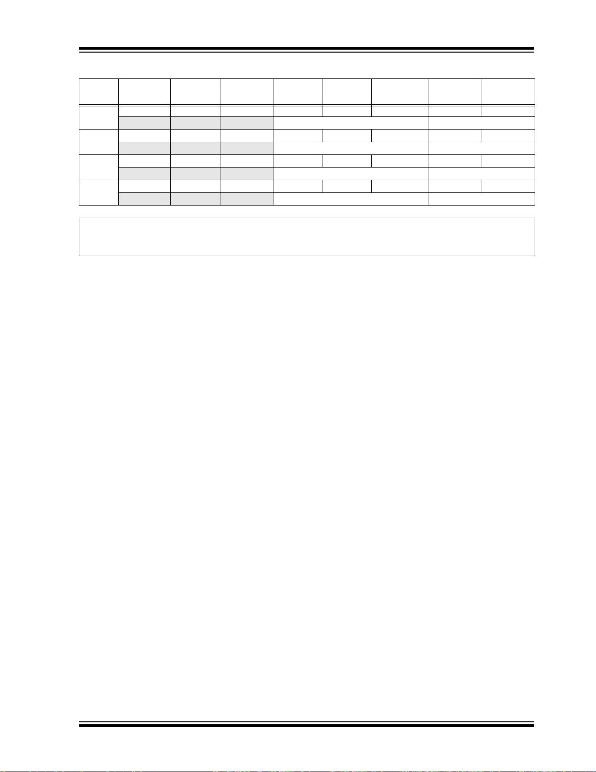
PIC32MX1XX/2XX
REGISTER 7-6: IPCx: INTERRUPT PRIORITY CONTROL REGISTER
Bit
Range
31:24
23:16
15:8
7:0
Bit
31/23/15/7
U-0 U-0 U-0 R/W-0 R/W-0 R/W-0 R/W-0 R/W-0
Bit
30/22/14/6
Bit
29/21/13/5
Bit
28/20/12/4
Bit
27/19/11/3
— — — IP03<2:0> IS03<1:0>
U-0 U-0 U-0 R/W-0 R/W-0 R/W-0 R/W-0 R/W-0
— — — IP02<2:0> IS02<1:0>
U-0 U-0 U-0 R/W-0 R/W-0 R/W-0 R/W-0 R/W-0
— — — IP01<2:0> IS01<1:0>
U-0 U-0 U-0 R/W-0 R/W-0 R/W-0 R/W-0 R/W-0
— — — IP00<2:0> IS00<1:0>
(1)
Bit
26/18/10/2
Bit
25/17/9/1
Legend:
R = Readable bit W = Writable bit U = Unimplemented bit, read as ‘0’
-n = Value at POR ‘1’ = Bit is set ‘0’ = Bit is cleared x = Bit is unknown
bit 31-29 Unimplemented: Read as ‘0’
bit 28-26 IP03<2:0>: Interrupt Priority bits
111 = Interrupt priority is 7
•
•
•
010 = Interrupt priority is 2
001 = Interrupt priority is 1
000 = Interrupt is disabled
bit 25-24 IS03<1:0>: Interrupt Subpriority bits
11 = Interrupt subpriority is 3
10 = Interrupt subpriority is 2
01 = Interrupt subpriority is 1
00 = Interrupt subpiority is 0
bit 23-21 Unimplemented: Read as ‘0’
bit 20-18 IP02<2:0>: Interrupt Priority bits
111 = Interrupt priority is 7
•
•
•
010 = Interrupt priority is 2
001 = Interrupt priority is 1
000 = Interrupt is disabled
bit 17-16 IS02<1:0>: Interrupt Subpriority bits
11 = Interrupt subpriority is 3
10 = Interrupt subpriority is 2
01 = Interrupt subpriority is 1
00 = Interrupt subpriority is 0
bit 15-13 Unimplemented: Read as ‘0’
bit 12-10 IP01<2:0>: Interrupt Priority bits
111 = Interrupt priority is 7
•
•
•
010 = Interrupt priority is 2
001 = Interrupt priority is 1
000 = Interrupt is disabled
Bit
24/16/8/0
Note 1: This register represents a generic definition of the IPCx register. Refer to Ta bl e 7 -1 for the exact bit
definitions.
© 2011-2012 Microchip Technology Inc. Preliminary DS61168D-page 93

PIC32MX1XX/2XX
REGISTER 7-6: IPCx: INTERRUPT PRIORITY CONTROL REGISTER
bit 9-8 IS01<1:0>: Interrupt Subpriority bits
11 = Interrupt subpriority is 3
10 = Interrupt subpriority is 2
01 = Interrupt subpriority is 1
00 = Interrupt subpriority is 0
bit 7-5 Unimplemented: Read as ‘0’
bit 4-2 IP00<2:0>: Interrupt Priority bits
111 = Interrupt priority is 7
•
•
•
010 = Interrupt priority is 2
001 = Interrupt priority is 1
000 = Interrupt is disabled
bit 1-0 IS00<1:0>: Interrupt Subpriority bits
11 = Interrupt subpriority is 3
10 = Interrupt subpriority is 2
01 = Interrupt subpriority is 1
00 = Interrupt subpriority is 0
Note 1: This register represents a generic definition of the IPCx register. Refer to Ta bl e 7 -1 for the exact bit
definitions.
(1)
(CONTINUED)
DS61168D-page 94 Preliminary © 2011-2012 Microchip Technology Inc.

8.0 OSCILLATOR CONFIGURATION
Note 1: This data sheet summarizes the features
of the PIC32MX1XX/2XX family of
devices. It is not intended to be a
comprehensive reference source. To
complement the information in this data
sheet, refer to Section 6. “Oscillator
Configuration” ( D S 6 111 2 ) in th e
“PIC32 Family Reference Manual”, which
is available from the Microchip web site
(www.microchip.com/PIC32).
2: Some registers and associated bits
described in this section may not be
available on all devices. Refer to
Section 4.0 “Memory Organization” in
this data sheet for device-specific register
and bit information.
The PIC32MX1XX/2XX oscillator system has the
following modules and features:
• A Total of four external and internal oscillator
options as clock sources
• On-Chip PLL with user-selectable input divider,
multiplier and output divider to boost operating
frequency on select internal and external
oscillator sources
• On-Chip user-selectable divisor postscaler on
select oscillator sources
• Software-controllable switching between
various clock sources
• A Fail-Safe Clock Monitor (FSCM) that detects
clock failure and permits safe application recovery
or shutdown
• Dedicated On-Chip PLL for USB peripheral
A block diagram of the oscillator system is provided in
Figure 8-1.
PIC32MX1XX/2XX
© 2011-2012 Microchip Technology Inc. Preliminary DS61168D-page 95

PIC32MX1XX/2XX
Timer1, RTCC
Clock Control Logic
Fail-Safe
Clock
Monitor
FSCM INT
FSCM Event
COSC<2:0>
NOSC<2:0>
OSWEN
FSCMEN<1:0>
PLL
Secondary Oscillator (SOSC)
SOSCEN and FSOSCEN
SOSCO
SOSCI
Primary Oscillator
P
OSC (XT, HS, EC)
CPU and Select Peripherals
Peripherals
FRCDIV<2:0>
WDT, PWRT
8 MHz typical
FRC
31.25 kHz typical
FRC
Oscillator
LPRC
Oscillator
SOSC
LPRC
FRCDIV
TUN<5:0>
div 16
Postscaler
FPLLIDIV<2:0>
PBDIV<1:0>
FRC/16
Postscaler
COSC<2:0>
FIN
div x
div y
PLLODIV<2:0>
div x
32.768 kHz
PLLMULT<2:0>
PBCLK (T
PB)
UF
IN = 4 MHz
PLL x24
USB Clock (48 MHz)
div 2
UPLLEN
UFRCEN
div x
UPLLIDIV<2:0>
UFIN
4 MHz ≤ FIN ≤ 5 MHz
C1
(3)
C2
(3)
XTAL
R
S
(1)
Enable
Notes: 1. A series resistor, RS, may be required for AT strip cut crystals.
2. The internal feedback resistor, R
F, is typically in the range of 2 to 10 MΩ.
3. Refer to Section 6. “Oscillator Configuration” (DS61112) in the “PIC32 Family Reference Manual” for help in determining the
best oscillator components.
4. PBCLK out is available on the OSC2 pin in certain clock modes.
5. USB PLL is available on PIC32MX2XX devices only.
OSC2
(4)
OSC1
R
F
(2)
To Internal
Logic
USB PLL
(5)
(POSC)
div 2
To A D C
SYSCLK
REFCLKI
REFCLKO
OE
To SPI
ROSEL<3:0>
POSC
FRC
LPRC
S
OSC
PBCLK
SYSCLK
XTPLL, HSPLL,
ECPLL, FRCPLL
System USB PLL N
M
512
----------+
⎝⎠
⎛⎞
RODIV<4:0>
(N)
ROTRIM<8:0>
(M)
÷
FIGURE 8-1: PIC32MX1XX/2XX FAMILY CLOCK DIAGRAM
DS61168D-page 96 Preliminary © 2011-2012 Microchip Technology Inc.

PIC32MX1XX/2XX
REGISTER 8-1: OSCCON: OSCILLATOR CONTROL REGISTER
Bit
Range
31:24
23:16
15:8
7:0
Bit
31/23/15/7
U-0 U-0 R/W-y R/W-y R/W-y R/W-0 R/W-0 R/W-1
Bit
30/22/14/6
Bit
29/21/13/5
Bit
28/20/12/4
Bit
27/19/11/3
— — PLLODIV<2:0> FRCDIV<2:0>
U-0 R-0 R-1 R/W-y R/W-y R/W-y R/W-y R/W-y
— SOSCRDY PBDIVRDY PBDIV<1:0> PLLMULT<2:0>
U-0 R-0 R-0 R-0 U-0 R/W-y R/W-y R/W-y
— COSC<2:0> — NOSC<2:0>
R/W-0 R-0 R-0 R/W-0 R/W-0 R/W-0 R/W-y R/W-0
CLKLOCK ULOCK
(2)
SLOCK SLPEN CF UFRCEN
(1)
Bit
26/18/10/2
Bit
25/17/9/1
(2)
SOSCEN OSWEN
Legend: y = Value set from Configuration bits on POR
R = Readable bit W = Writable bit U = Unimplemented bit, read as ‘0’
-n = Value at POR ‘1’ = Bit is set ‘0’ = Bit is cleared x = Bit is unknown
bit 31-30 Unimplemented: Read as ‘0’
bit 29-27 PLLODIV<2:0>: Output Divider for PLL
111 = PLL output divided by 256
110 = PLL output divided by 64
101 = PLL output divided by 32
100 = PLL output divided by 16
011 = PLL output divided by 8
010 = PLL output divided by 4
001 = PLL output divided by 2
000 = PLL output divided by 1
bit 26-24 FRCDIV<2:0>: Internal Fast RC (FRC) Oscillator Clock Divider bits
111 = FRC divided by 256
110 = FRC divided by 64
101 = FRC divided by 32
100 = FRC divided by 16
011 = FRC divided by 8
010 = FRC divided by 4
001 = FRC divided by 2 (default setting)
000 = FRC divided by 1
bit 23 Unimplemented: Read as ‘0’
bit 22 SOSCRDY: Secondary Oscillator (S
OSC) Ready Indicator bit
1 = Indicates that the Secondary Oscillator is running and is stable
0 = Secondary Oscillator is still warming up or is turned off
bit 21 PBDIVRDY: Peripheral Bus Clock (PBCLK) Divisor Ready bit
1 = PBDIV<1:0> bits can be written
0 = PBDIV<1:0> bits cannot be written
bit 20-19 PBDIV<1:0>: Peripheral Bus Clock (PBCLK) Divisor bits
11 = PBCLK is SYSCLK divided by 8 (default)
10 = PBCLK is SYSCLK divided by 4
01 = PBCLK is SYSCLK divided by 2
00 = PBCLK is SYSCLK divided by 1
Bit
24/16/8/0
Note 1: Writes to this register require an unlock sequence. Refer to Section 6. “Oscillator” (DS61112) in the
“PIC32 Family Reference Manual” for details.
2: This bit is available on PIC32MX2XX devices only.
© 2011-2012 Microchip Technology Inc. Preliminary DS61168D-page 97

PIC32MX1XX/2XX
REGISTER 8-1: OSCCON: OSCILLATOR CONTROL REGISTER
bit 18-16 PLLMULT<2:0>: Phase-Locked Loop (PLL) Multiplier bits
111 = Clock is multiplied by 24
110 = Clock is multiplied by 21
101 = Clock is multiplied by 20
100 = Clock is multiplied by 19
011 = Clock is multiplied by 18
010 = Clock is multiplied by 17
001 = Clock is multiplied by 16
000 = Clock is multiplied by 15
bit 15 Unimplemented: Read as ‘0’
bit 14-12 COSC<2:0>: Current Oscillator Selection bits
111 = Internal Fast RC (FRC) Oscillator divided by OSCCON<FRCDIV> bits
110 = Internal Fast RC (FRC) Oscillator divided by 16
101 = Internal Low-Power RC (LPRC) Oscillator
100 = Secondary Oscillator (S
011 = Primary Oscillator (P
010 = Primary Oscillator (POSC) (XT, HS or EC)
001 = Internal Fast RC Oscillator with PLL module via Postscaler (FRCPLL)
000 = Internal Fast RC (FRC) Oscillator
bit 11 Unimplemented: Read as ‘0’
bit 10-8 NOSC<2:0>: New Oscillator Selection bits
111 = Internal Fast RC Oscillator (FRC) divided by OSCCON<FRCDIV> bits
110 = Internal Fast RC Oscillator (FRC) divided by 16
101 = Internal Low-Power RC (LPRC) Oscillator
100 = Secondary Oscillator (S
011 = Primary Oscillator with PLL module (XTPLL, HSPLL or ECPLL)
010 = Primary Oscillator (XT, HS or EC)
001 = Internal Fast Internal RC Oscillator with PLL module via Postscaler (FRCPLL)
000 = Internal Fast Internal RC Oscillator (FRC)
On Reset, these bits are set to the value of the FNOSC Configuration bits (DEVCFG1<2:0>).
bit 7 CLKLOCK: Clock Selection Lock Enable bit
If clock switching and monitoring is
1 = Clock and PLL selections are locked
0 = Clock and PLL selections are not locked and may be modified
OSC)
OSC) with PLL module (XTPLL, HSPLL or ECPLL)
OSC)
disabled (FCKSM<1:0> = 1x):
(1)
If clock switching and monitoring is enabled (FCKSM<1:0> =
Clock and PLL selections are never locked and may be modified.
bit 6 ULOCK: USB PLL Lock Status bit
1 = Indicates that the USB PLL module is in lock or USB PLL module start-up timer is satisfied
0 = Indicates that the USB PLL module is out of lock or USB PLL module start-up timer is in progress or
USB PLL is disabled
bit 5 SLOCK: PLL Lock Status bit
1 = PLL module is in lock or PLL module start-up timer is satisfied
0 = PLL module is out of lock, PLL start-up timer is running or PLL is disabled
bit 4 SLPEN: Sleep Mode Enable bit
1 = Device will enter Sleep mode when a WAIT instruction is executed
0 = Device will enter Idle mode when a WAIT instruction is executed
bit 3 CF: Clock Fail Detect bit
1 = FSCM has detected a clock failure
0 = No clock failure has been detected
Note 1: Writes to this register require an unlock sequence. Refer to Section 6. “Oscillator” (DS61112) in the
“PIC32 Family Reference Manual” for details.
2: This bit is available on PIC32MX2XX devices only.
DS61168D-page 98 Preliminary © 2011-2012 Microchip Technology Inc.
(2)
0x):

PIC32MX1XX/2XX
REGISTER 8-1: OSCCON: OSCILLATOR CONTROL REGISTER
bit 2 UFRCEN: USB FRC Clock Enable bit
1 = Enable FRC as the clock source for the USB clock source
0 = Use the Primary Oscillator or USB PLL as the USB clock source
bit 1 SOSCEN: Secondary Oscillator (SOSC) Enable bit
1 = Enable Secondary Oscillator
0 = Disable Secondary Oscillator
bit 0 OSWEN: Oscillator Switch Enable bit
1 = Initiate an oscillator switch to selection specified by NOSC<2:0> bits
0 = Oscillator switch is complete
Note 1: Writes to this register require an unlock sequence. Refer to Section 6. “Oscillator” (DS61112) in the
“PIC32 Family Reference Manual” for details.
2: This bit is available on PIC32MX2XX devices only.
(2)
(1)
© 2011-2012 Microchip Technology Inc. Preliminary DS61168D-page 99

PIC32MX1XX/2XX
REGISTER 8-2: OSCTUN: FRC TUNING REGISTER
Bit
Range
31:24
23:16
15:8
7:0
Bit
31/23/15/7
U-0 U-0 U-0 U-0 U-0 U-0 U-0 U-0
Bit
30/22/14/6
Bit
29/21/13/5
Bit
28/20/12/4
— — — — — — — —
U-0 R-0 U-0 U-0 U-0 U-0 U-0 U-0
— — — — — — — —
U-0 R-0 U-0 U-0 U-0 U-0 U-0 U-0
— — — — — — — —
U-0 U-0 R/W-0 R/W-0 R/W-0 R/W-0 R/W-0 R/W-0
— — TUN<5:0>
(1)
Bit
27/19/11/3
Bit
26/18/10/2
(2)
Bit
25/17/9/1
24/16/8/0
Legend: y = Value set from Configuration bits on POR
R = Readable bit W = Writable bit U = Unimplemented bit, read as ‘0’
-n = Value at POR ‘1’ = Bit is set ‘0’ = Bit is cleared x = Bit is unknown
bit 31-6 Unimplemented: Read as ‘0’
bit 5-0 TUN<5:0>: FRC Oscillator Tuning bits
(2)
100000 = Center frequency -12.5%
100001 =
•
•
•
111111 =
000000 = Center frequency. Oscillator runs at minimal frequency (8 MHz)
000001 =
•
•
•
011110 =
011111 = Center frequency +12.5%
Bit
Note 1: Writes to this register require an unlock sequence. Refer to Section 6. “Oscillator” (D S 6 111 2 ) in the
“PIC32 Family Reference Manual” for details.
2: OSCTUN functionality has been provided to help customers compensate for temperature effects on the
FRC frequency over a wide range of temperatures. The tuning step size is an approximation, and is neither
characterized, nor tested.
DS61168D-page 100 Preliminary © 2011-2012 Microchip Technology Inc.
 Loading...