

Datasheet PIC32MX110F016B, PIC32MX110F016C, PIC32MX110F016D, PIC32MX120F032B, PIC32MX120F032C Datasheet
...
PIC32MX1XX/2XX 28/36/44-PIN
32-bit Microcontrollers (up to 256 KB Flash and 64 KB SRAM) with
Audio and Graphics Interfaces, USB, and Advanced Analog
Operating Conditions
• 2.3V to 3.6V, -40ºC to +105ºC, DC to 40 MHz
• 2.3V to 3.6V, -40ºC to +85ºC, DC to 50 MHz
Core: 50 MHz/83 DMIPS MIPS32® M4K
•MIPS16e® mode for up to 40% smaller code size
• Code-efficient (C and Assembly) architecture
• Single-cycle (MAC) 32x16 and two-cycle 32x32 multiply
®
Clock Management
• 0.9% internal oscillator
• Programmable PLLs and oscillator clock sources
• Fail-Safe Clock Monitor (FSCM)
• Independent Watchdog Timer
• Fast wake-up and start-up
Power Management
• Low-power management modes (Sleep and Idle)
• Integrated Power-on Reset and Brown-out Reset
• 0.5 mA/MHz dynamic current (typical)
PD
•44 μA I
current (typical)
Audio Interface Features
• Data communication: I2S, LJ, RJ, and DSP modes
• Control interface: SPI and I
• Master clock:
- Generation of fractional clock frequencies
- Can be synchronized with USB clock
- Can be tuned in run-time
2
C
Advanced Analog Features
• ADC Module:
- 10-bit 1.1 Msps rate with one S&H
- Up to 10 analog inputs on 28-pin devices and 13
analog inputs on 44-pin devices
• Flexible and independent ADC trigger sources
• Charge Time Measurement Unit (CTMU):
- Supports mTouch™ capacitive touch sensing
- Provides high-resolution time measurement (1 ns)
- On-chip temperature measurement capability
• Comparators:
- Up to three Analog Comparator modules
- Programmable references with 32 voltage points
Timers/Output Compare/Input Capture
• Five General Purpose Timers:
- Five 16-bit and up to two 32-bit Timers/Counters
• Five Output Compare (OC) modules
• Five Input Capture (IC) modules
• Peripheral Pin Select (PPS) to allow function remap
• Real-Time Clock and Calendar (RTCC) module
Communication Interfaces
• USB 2.0-compliant Full-speed OTG controller
• Two UART modules (12.5 Mbps):
- Supports LIN 2.0 protocols and IrDA
• Two 4-wire SPI modules (25 Mbps)
2
•Two I
• PPS to allow function remap
• Parallel Master Port (PMP)
C modules (up to 1 Mbaud) with SMBus support
®
support
Direct Memory Access (DMA)
• Four channels of hardware DMA with automatic data
size detection
• Two additional channels dedicated for USB
• Programmable Cyclic Redundancy Check (CRC)
Input/Output
• 10 mA source/sink on all I/O pins and up to 14 mA on
non-standard V
• 5V-tolerant pins
• Selectable open drain, pull-ups, and pull-downs
• External interrupts on all I/O pins
OH
Class B Support
• Class B Safety Library, IEC 60730
Debugger Development Support
• In-circuit and in-application programming
•4-wire MIPS
• Unlimited program and six complex data breakpoints
• IEEE 1149.2-compatible (JTAG) boundary scan
®
Enhanced JTAG interface
Packages
Type SOIC SSOP SPDIP QFN VTLA TQFP
Pin Count 28 28 28 28 44 36 44 44
I/O Pins (up to) 21 21 21 21 34 25 34 34
Contact/Lead Pitch 1.27 0.65 0.100'' 0.65 0.65 0.50 0.50 0.80
Dimensions 17.90x7.50x2.65 10.2x5.3x2 1.365''x.285''x.135'' 6x6x0.9 8x8x0.9 5x5x0.9 6x6x0.9 10x10x1
Note: All dimensions are in millimeters (mm) unless specified.
2011-2019 Microchip Technology Inc. DS60001168L-page 1

PIC32MX1XX/2XX 28/36/44-PIN FAMILY
TABLE 1: PIC32MX1XX 28/36/44-PIN GENERAL PURPOSE FAMILY FEATURES
Remappable Peripherals
(1)
(3)
S
UART
2
SPI/I
Analog Comparators
External Interrupts
Device
PIC32MX110F016B 28 16+3 4 20 5/5/5 2 2 5 3 N 2 Y 4/0 Y 10 Y 21 Y
PIC32MX110F016C 36 16+3 4 24 5/5/5 2 2 5 3 N 2 Y 4/0 Y 12 Y 25 Y VTLA
PIC32MX110F016D 44 16+3 4 32 5/5/5 2 2 5 3 N 2 Y 4/0 Y 13 Y 35 Y
PIC32MX120F032B 28 32+3 8 20 5/5/5 2 2 5 3 N 2 Y 4/0 Y 10 Y 21 Y
PIC32MX120F032C 36 32+3 8 24 5/5/5 2 2 5 3 N 2 Y 4/0 Y 12 Y 25 Y VTLA
PIC32MX120F032D 44 32+3 8 32 5/5/5 2 2 5 3 N 2 Y 4/0 Y 13 Y 35 Y
PIC32MX130F064B 28 64+3 16 20 5/5/5 2 2 5 3 N 2 Y 4/0 Y 10 Y 21 Y
PIC32MX130F064C 36 64+3 16 24 5/5/5 2 2 5 3 N 2 Y 4/0 Y 12 Y 25 Y VTLA
PIC32MX130F064D 44 64+3 16 32 5/5/5 2 2 5 3 N 2 Y 4/0 Y 13 Y 35 Y
PIC32MX150F128B 28 128+3 32 20 5/5/5 2 2 5 3 N 2 Y 4/0 Y 10 Y 21 Y
PIC32MX150F128C 36 128+3 32 24 5/5/5 2 2 5 3 N 2 Y 4/0 Y 12 Y 25 Y VTLA
PIC32MX150F128D 44 128+3 32 32 5/5/5 2 2 5 3 N 2 Y 4/0 Y 13 Y 35 Y
PIC32MX130F256B 28 256+3 16 20 5/5/5 2 2 5 3 N 2 Y 4/0 Y 10 Y 21 Y
PIC32MX130F256D 44 256+3 16 32 5/5/5 2 2 5 3 N 2 Y 4/0 Y 13 Y 35 Y
PIC32MX170F256B 28 256+3 64 20 5/5/5 2 2 5 3 N 2 Y 4/0 Y 10 Y 21 Y
PIC32MX170F256D 44 256+3 64 32 5/5/5 2 2 5 3 N 2 Y 4/0 Y 13 Y 35 Y
Note 1: This device features 3 KB of boot Flash memory.
2: Four out of five timers are remappable.
3: Four out of five external interrupts are remappable.
Pins
Program Memory (KB)
Data Memory (KB)
Remappable Pins
/Capture/Compare
(2)
Timers
C
2
I
PMP
USB On-The-Go (OTG)
CTMU
DMA Channels
(Programmable/Dedicated)
RTCC
10-bit 1 Msps ADC (Channels)
I/O Pins
JTAG
SOIC,
SSOP,
SPDIP,
QFN
VTLA,
TQFP,
QFN
SOIC,
SSOP,
SPDIP,
QFN
VTLA,
TQFP,
QFN
SOIC,
SSOP,
SPDIP,
QFN
VTLA,
TQFP,
QFN
SOIC,
SSOP,
SPDIP,
QFN
VTLA,
TQFP,
QFN
SSOP,
SPDIP,
QFN
VTLA,
TQFP,
QFN
SOIC,
SSOP,
SPDIP,
QFN
VTLA,
TQFP,
QFN
Packages
DS60001168L-page 2 2011-2019 Microchip Technology Inc.

PIC32MX1XX/2XX 28/36/44-PIN FAMILY
TABLE 2: PIC32MX2XX 28/36/44-PIN USB FAMILY FEATURES
Remappable Peripherals
(1)
(3)
S
Device
PIC32MX210F016B 28 16+3 4 19 5/5/5 2 2 5 3 Y 2 Y 4/2 Y 9 Y 19 Y
PIC32MX210F016C 36 16+3 4 23 5/5/5 2 2 5 3 Y 2 Y 4/2 Y 12 Y 25 Y VTLA
PIC32MX210F016D 44 16+3 4 31 5/5/5 2 2 5 3 Y 2 Y 4/2 Y 13 Y 33 Y
PIC32MX220F032B 28 32+3 8 19 5/5/5 2 2 5 3 Y 2 Y 4/2 Y 9 Y 19 Y
PIC32MX220F032C 36 32+3 8 23 5/5/5 2 2 5 3 Y 2 Y 4/2 Y 12 Y 23 Y VTLA
PIC32MX220F032D 44 32+3 8 31 5/5/5 2 2 5 3 Y 2 Y 4/2 Y 13 Y 33 Y
PIC32MX230F064B 28 64+3 16 19 5/5/5 2 2 5 3 Y 2 Y 4/2 Y 9 Y 19 Y
PIC32MX230F064C 36 64+3 16 23 5/5/5 2 2 5 3 Y 2 Y 4/2 Y 12 Y 23 Y VTLA
PIC32MX230F064D 44 64+3 16 31 5/5/5 2 2 5 3 Y 2 Y 4/2 Y 13 Y 33 Y
PIC32MX250F128B 28 128+3 32 19 5/5/5 2 2 5 3 Y 2 Y 4/2 Y 9 Y 19 Y
PIC32MX250F128C 36 128+3 32 23 5/5/5 2 2 5 3 Y 2 Y 4/2 Y 12 Y 23 Y VTLA
PIC32MX250F128D 44 128+3 32 31 5/5/5 2 2 5 3 Y 2 Y 4/2 Y 13 Y 33 Y
PIC32MX230F256B 28 256+3 16 19 5/5/5 2 2 5 3 Y 2 Y 4/2 Y 9 Y 19 Y
PIC32MX230F256D 44 256+3 16 31 5/5/5 2 2 5 3 Y 2 Y 4/2 Y 13 Y 33 Y
PIC32MX270F256B 28 256+3 64 19 5/5/5 2 2 5 3 Y 2 Y 4/2 Y 9 Y 19 Y
PIC32MX270F256D
Note 1: This device features 3 KB of boot Flash memory.
2: Four out of five timers are remappable.
3: Four out of five external interrupts are remappable.
Pins
/Capture/Compare
Data Memory (KB)
Program Memory (KB)
44 256+3 64 31 5/5/5 2 2 5 3 Y 2 Y 4/2 Y 13 Y 33 Y
(2)
Remappable Pins
Timers
UART
2
SPI/I
Analog Comparators
External Interrupts
USB On-The-Go (OTG)
C
2
I
PMP
CTMU
DMA Channels
(Programmable/Dedicated)
RTCC
10-bit 1 Msps ADC (Channels)
JTAG
I/O Pins
SOIC,
SSOP,
SPDIP,
QFN
VTLA,
TQFP,
QFN
SOIC,
SSOP,
SPDIP,
QFN
VTLA,
TQFP,
QFN
SOIC,
SSOP,
SPDIP,
QFN
VTLA,
TQFP,
QFN
SOIC,
SSOP,
SPDIP,
QFN
VTLA,
TQFP,
QFN
SSOP,
SPDIP,
QFN
VTLA,
TQFP,
QFN
SOIC,
SSOP,
SPDIP,
QFN
VTLA,
TQFP,
QFN
Packages
2011-2019 Microchip Technology Inc. DS60001168L-page 3

PIC32MX1XX/2XX 28/36/44-PIN FAMILY
PIC32MX110F016B
PIC32MX120F032B
PIC32MX130F064B
PIC32MX130F256B
PIC32MX150F128B
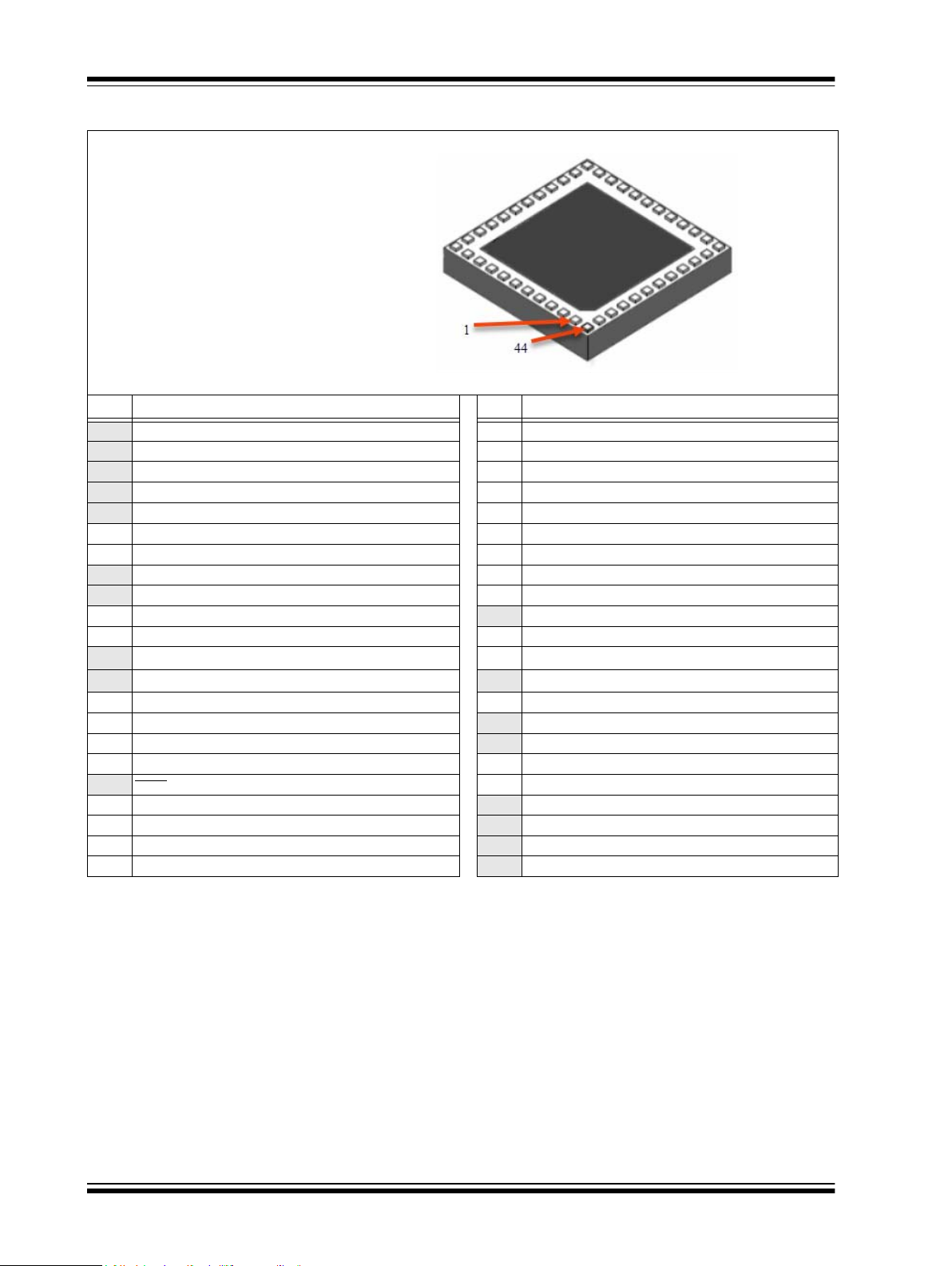
28-PIN SOIC, SPDIP, SSOP (TOP VIEW)
(1,2,3)
28
SPDIPSOIC
PIC32MX170F256B
SSOP
1
28
1281
Pin Diagrams
TABLE 3: PIN NAMES FOR 28-PIN GENERAL PURPOSE DEVICES
Pin # Full Pin Name Pin # Full Pin Name
1
MCLR
2
REF
+/CV
REF
V
3
REF
V
4
PGED1/AN2/C1IND/C2INB/C3IND/RPB0/RB0
5
PGEC1/AN3/C1INC/C2INA/RPB1/CTED12/RB1
6
AN4/C1INB/C2IND/RPB2/SDA2/CTED13/RB2
7
AN5/C1INA/C2INC/RTCC/RPB3/SCL2/RB3
8
SS
V
9
OSC1/CLKI/RPA2/RA2
10
OSC2/CLKO/RPA3/PMA0/RA3
11
SOSCI/RPB4/RB4
12
SOSCO/RPA4/T1CK/CTED9/PMA1/RA4
13
DD
V
14
PGED3/RPB5/PMD7/RB5
Note 1: The RPn pins can be used by remappable peripherals. See Table 1 for the available peripherals and Section 11.3 “Peripheral Pin
2: Every I/O port pin (RAx-RCx) can be used as a change notification pin (CNAx-CNCx). See Section 11.0 “I/O Ports” for more information.
3: Shaded pins are 5V tolerant.
+/AN0/C3INC/RPA0/CTED1/RA0
-/CV
REF
-/AN1/RPA1/CTED2/RA1
Select” for restrictions.
15
PGEC3/RPB6/PMD6/RB6
16
TDI/RPB7/CTED3/PMD5/INT0/RB7
17
TCK/RPB8/SCL1/CTED10/PMD4/RB8
18
TDO/RPB9/SDA1/CTED4/PMD3/RB9
19
SS
V
20
CAP
V
21
PGED2/RPB10/CTED11/PMD2/RB10
22
PGEC2/TMS/RPB11/PMD1/RB11
23
AN12/PMD0/RB12
24
AN11/RPB13/CTPLS/PMRD/RB13
25
REFOUT
CV
26
AN9/C3INA/RPB15/SCK2/CTED6/PMCS1/RB15
27
AV
28
AV
/AN10/C3INB/RPB14/SCK1/CTED5/PMWR/RB14
SS
DD
DS60001168L-page 4 2011-2019 Microchip Technology Inc.

PIC32MX1XX/2XX 28/36/44-PIN FAMILY
PIC32MX210F016B
PIC32MX220F032B
PIC32MX230F064B
PIC32MX230F256B
PIC32MX250F128B
28-PIN SOIC, SPDIP, SSOP (TOP VIEW)
(1,2,3)
PIC32MX270F256B
28
SPDIPSOICSSOP
1
28
1281
TABLE 4: PIN NAMES FOR 28-PIN USB DEVICES
Pin # Full Pin Name Pin # Full Pin Name
1
MCLR
2
PGED3/V
REF
+/CV
REF
+/AN0/C3INC/RPA0/CTED1/PMD7/RA0
3
PGEC3/V
REF
-/CV
REF
-/AN1/RPA1/CTED2/PMD6/RA1
4
PGED1/AN2/C1IND/C2INB/C3IND/RPB0/PMD0/RB0
5
PGEC1/AN3/C1INC/C2INA/RPB1/CTED12/PMD1/RB1
6
AN4/C1INB/C2IND/RPB2/SDA2/CTED13/PMD2/RB2
7
AN5/C1INA/C2INC/RTCC/RPB3/SCL2/PMWR/RB3
8
SS
V
9
OSC1/CLKI/RPA2/RA2
10
OSC2/CLKO/RPA3/PMA0/RA3
11
SOSCI/RPB4/RB4
12
SOSCO/RPA4/T1CK/CTED9/PMA1/RA4
13
DD
V
14
TMS/RPB5/USBID/RB5
Note 1: The RPn pins can be used by remappable peripherals. See Table 1 for the available peripherals and Section 11.3 “Peripheral Pin
Select” for restrictions.
2: Every I/O port pin (RAx-RCx) can be used as a change notification pin (CNAx-CNCx). See Section 11.0 “I/O Ports” for more informa-
tion.
3: Shaded pins are 5V tolerant.
15
BUS
V
16
TDI/RPB7/CTED3/PMD5/INT0/RB7
17
TCK/RPB8/SCL1/CTED10/PMD4/RB8
18
TDO/RPB9/SDA1/CTED4/PMD3/RB9
19
V
SS
20
V
CAP
21
PGED2/RPB10/D+/CTED11/RB10
22
PGEC2/RPB11/D-/RB11
23
USB3V
3
V
24
AN11/RPB13/CTPLS/PMRD/RB13
25
REFOUT
CV
26
AN9/C3INA/RPB15/SCK2/CTED6/PMCS1/RB15
27
AV
28
AV
/AN10/C3INB/RPB14/V
SS
DD
BUSON
/SCK1/CTED5/RB14
2011-2019 Microchip Technology Inc. DS60001168L-page 5

PIC32MX1XX/2XX 28/36/44-PIN FAMILY
PIC32MX110F016B
PIC32MX120F032B
PIC32MX130F064B
PIC32MX130F256B
PIC32MX150F128B
1
28
28-PIN QFN (TOP VIEW)
(1,2,3.4)
PIC32MX170F256B
TABLE 5: PIN NAMES FOR 28-PIN GENERAL PURPOSE DEVICES
Pin # Full Pin Name Pin # Full Pin Name
1
PGED1/AN2/C1IND/C2INB/C3IND/RPB0/RB0
2
PGEC1/AN3/C1INC/C2INA/RPB1/CTED12/RB1
3
AN4/C1INB/C2IND/RPB2/SDA2/CTED13/RB2
4
AN5/C1INA/C2INC/RTCC/RPB3/SCL2/RB3
5
V
SS
6
OSC1/CLKI/RPA2/RA2
7
OSC2/CLKO/RPA3/PMA0/RA3
8
SOSCI/RPB4/RB4
9
SOSCO/RPA4/T1CK/CTED9/PMA1/RA4
10
DD
V
11
PGED3/RPB5/PMD7/RB5
12
PGEC3/RPB6/PMD6/RB6
13
TDI/RPB7/CTED3/PMD5/INT0/RB7
14
TCK/RPB8/SCL1/CTED10/PMD4/RB8
Note 1: The RPn pins can be used by remappable peripherals. See Table 1 for the available peripherals and Section 11.3 “Peripheral Pin
Select” for restrictions.
2: Every I/O port pin (RAx-RCx) can be used as a change notification pin (CNAx-CNCx). See Section 11.0 “I/O Ports” for more information.
3: The metal plane at the bottom of the device is not connected to any pins and is recommended to be connected to V
4: Shaded pins are 5V tolerant.
15
TDO/RPB9/SDA1/CTED4/PMD3/RB9
16
SS
V
17
CAP
V
18
PGED2/RPB10/CTED11/PMD2/RB10
19
PGEC2/TMS/RPB11/PMD1/RB11
20
AN12/PMD0/RB12
21
AN11/RPB13/CTPLS/PMRD/RB13
22
REFOUT
CV
23
AN9/C3INA/RPB15/SCK2/CTED6/PMCS1/RB15
24
AV
25
AV
26
MCLR
27
V
28
V
/AN10/C3INB/RPB14/SCK1/CTED5/PMWR/RB14
SS
DD
REF
+/CV
REF
+/AN0/C3INC/RPA0/CTED1/RA0
REF
-/CV
REF
-/AN1/RPA1/CTED2/RA1
SS
externally.
DS60001168L-page 6 2011-2019 Microchip Technology Inc.

PIC32MX1XX/2XX 28/36/44-PIN FAMILY
28-PIN QFN (TOP VIEW)
(1,2,3,4)
PIC32MX210F016B
PIC32MX220F032B
PIC32MX230F064B
PIC32MX230F256B
PIC32MX250F128B
PIC32MX270F256B
1
28
TABLE 6: PIN NAMES FOR 28-PIN USB DEVICES
Pin # Full Pin Name Pin # Full Pin Name
1
PGED1/AN2/C1IND/C2INB/C3IND/RPB0/PMD0/RB0
2
PGEC1/AN3/C1INC/C2INA/RPB1/CTED12/PMD1/RB1
3
AN4/C1INB/C2IND/RPB2/SDA2/CTED13/PMD2/RB2
4
AN5/C1INA/C2INC/RTCC/RPB3/SCL2/PMWR/RB3
5
V
SS
6
OSC1/CLKI/RPA2/RA2
7
OSC2/CLKO/RPA3/PMA0/RA3
8
SOSCI/RPB4/RB4
9
SOSCO/RPA4/T1CK/CTED9/PMA1/RA4
10
DD
V
11
TMS/RPB5/USBID/RB5
12
BUS
V
13
TDI/RPB7/CTED3/PMD5/INT0/RB7
14
TCK/RPB8/SCL1/CTED10/PMD4/RB8
Note 1: The RPn pins can be used by remappable peripherals. See Table 1 for the available peripherals and Section 11.3 “Peripheral Pin
Select” for restrictions.
2: Every I/O port pin (RAx-RCx) can be used as a change notification pin (CNAx-CNCx). See Section 11.0 “I/O Ports” for more information.
3: The metal plane at the bottom of the device is not connected to any pins and is recommended to be connected to V
4: Shaded pins are 5V tolerant.
15
TDO/RPB9/SDA1/CTED4/PMD3/RB9
16
SS
V
17
CAP
V
18
PGED2/RPB10/D+/CTED11/RB10
19
PGEC2/RPB11/D-/RB11
20
USB3V
3
V
21
AN11/RPB13/CTPLS/PMRD/RB13
22
REFOUT
CV
23
AN9/C3INA/RPB15/SCK2/CTED6/PMCS1/RB15
24
AV
25
AV
26
MCLR
27
PGED3/V
28
PGEC3/V
/AN10/C3INB/RPB14/V
SS
DD
REF
+/CV
REF
-/CV
REF
+/AN0/C3INC/RPA0/CTED1/PMD7/RA0
REF
-/AN1/RPA1/CTED2/PMD6/RA1
BUSON
/SCK1/CTED5/RB14
SS
externally.
2011-2019 Microchip Technology Inc. DS60001168L-page 7

PIC32MX1XX/2XX 28/36/44-PIN FAMILY
PIC32MX110F016C
PIC32MX120F032C
PIC32MX130F064C
PIC32MX150F128C
36-PIN VTLA (BOTTOM VIEW)
(1,2,3,5)
36
1
TABLE 7: PIN NAMES FOR 36-PIN GENERAL PURPOSE DEVICES
Pin # Full Pin Name Pin # Full Pin Name
1
AN4/C1INB/C2IND/RPB2/SDA2/CTED13/RB2
2
AN5/C1INA/C2INC/RTCC/RPB3/SCL2/RB3
3
4
5
6
7
8
9
10
11
12
13
14
15
16
17
18
Note 1: The RPn pins can be used by remappable peripherals. See Table 1 for the available peripherals and Section 11.3 “Peripheral Pin
(4)
PGED4
PGEC4
V
V
OSC1/CLKI/RPA2/RA2
OSC2/CLKO/RPA3/PMA0/RA3
SOSCI/RPB4/RB4
SOSCO/RPA4/T1CK/CTED9/PMA1/RA4
RPC3/RC3
V
V
V
PGED3/RPB5/PMD7/RB5
PGEC3/RPB6/PMD6/RB6
TDI/RPB7/CTED3/PMD5/INT0/RB7
TCK/RPB8/SCL1/CTED10/PMD4/RB8
2: Every I/O port pin (RAx-RCx) can be used as a change notification pin (CNAx-CNCx). See Section 11.0 “I/O Ports” for more information.
3: The metal plane at the bottom of the device is not connected to any pins and is recommended to be connected to V
4: This pin function is not available on PIC32MX110F016C and PIC32MX120F032C devices.
5: Shaded pins are 5V tolerant.
/AN6/RPC0/RC0
(4)
/AN7/RPC1/RC1
DD
SS
SS
DD
DD
Select” for restrictions.
19
TDO/RPB9/SDA1/CTED4/PMD3/RB9
20
RPC9/CTED7/RC9
21
V
SS
22
V
CAP
23
DD
V
24
PGED2/RPB10/CTED11/PMD2/RB10
25
PGEC2/TMS/RPB11/PMD1/RB11
26
AN12/PMD0/RB12
27
AN11/RPB13/CTPLS/PMRD/RB13
28
REFOUT
CV
29
AN9/C3INA/RPB15/SCK2/CTED6/PMCS1/RB15
30
AV
31
AV
32
MCLR
33
V
34
V
35
PGED1/AN2/C1IND/C2INB/C3IND/RPB0/RB0
36
PGEC1/AN3/C1INC/C2INA/RPB1/CTED12/RB1
/AN10/C3INB/RPB14/SCK1/CTED5/PMWR/RB14
SS
DD
REF
+/CV
REF
+/AN0/C3INC/RPA0/CTED1/RA0
REF
-/CV
REF
-/AN1/RPA1/CTED2/RA1
SS
externally.
DS60001168L-page 8 2011-2019 Microchip Technology Inc.

PIC32MX1XX/2XX 28/36/44-PIN FAMILY
PIC32MX210F016C
PIC32MX220F032C
PIC32MX230F064C
PIC32MX250F128C
36-PIN VTLA (BOTTOM VIEW)
(1,2,3,5)
36
1
TABLE 8: PIN NAMES FOR 36-PIN USB DEVICES
Pin # Full Pin Name Pin # Full Pin Name
1
AN4/C1INB/C2IND/RPB2/SDA2/CTED13/PMD2/RB2
2
AN5/C1INA/C2INC/RTCC/RPB3/SCL2/PMWR/RB3
3
4
5
6
7
8
9
10
11
12
13
14
15
16
17
18
Note 1: The RPn pins can be used by remappable peripherals. See Table 1 for the available peripherals and Section 11.3 “Peripheral Pin
(4)
/AN6/RPC0/RC0
PGED4
(4)
PGEC4
/AN7/RPC1/RC1
V
DD
SS
V
OSC1/CLKI/RPA2/RA2
OSC2/CLKO/RPA3/PMA0/RA3
SOSCI/RPB4/RB4
SOSCO/RPA4/T1CK/CTED9/PMA1/RA4
AN12/RPC3/RC3
SS
V
V
DD
V
DD
TMS/RPB5/USBID/RB5
BUS
V
TDI/RPB7/CTED3/PMD5/INT0/RB7
TCK/RPB8/SCL1/CTED10/PMD4/RB8
Select” for restrictions.
2: Every I/O port pin (RAx-RCx) can be used as a change notification pin (CNAx-CNCx). See Section 11.0 “I/O Ports” for more information.
3: The metal plane at the bottom of the device is not connected to any pins and is recommended to be connected to V
4: This pin function is not available on PIC32MX210F016C and PIC32MX120F032C devices.
5: Shaded pins are 5V tolerant.
19
TDO/RPB9/SDA1/CTED4/PMD3/RB9
20
RPC9/CTED7/RC9
21
V
SS
22
V
CAP
23
V
DD
24
PGED2/RPB10/D+/CTED11/RB10
25
PGEC2/RPB11/D-/RB11
26
USB3V
3
V
27
AN11/RPB13/CTPLS/PMRD/RB13
28
REFOUT
CV
29
AN9/C3INA/RPB15/SCK2/CTED6/PMCS1/RB15
30
AV
31
AV
32
MCLR
33
PGED3/V
34
PGEC3/V
35
PGED1/AN2/C1IND/C2INB/C3IND/RPB0/PMD0/RB0
36
PGEC1/AN3/C1INC/C2INA/RPB1/CTED12/PMD1/RB1
/AN10/C3INB/RPB14/V
SS
DD
REF
+/CV
REF
-/CV
REF
+/AN0/C3INC/RPA0/CTED1/PMD7/RA0
REF
-/AN1/RPA1/CTED2/PMD6/RA1
BUSON
/SCK1/CTED5/RB14
SS
externally.
2011-2019 Microchip Technology Inc. DS60001168L-page 9

PIC32MX1XX/2XX 28/36/44-PIN FAMILY
PIC32MX110F016D
PIC32MX120F032D
PIC32MX130F064D
PIC32MX130F256D
PIC32MX150F128D
1
44
44-PIN QFN (TOP VIEW)
(1,2,3,5)
PIC32MX170F256D
TABLE 9: PIN NAMES FOR 44-PIN GENERAL PURPOSE DEVICES
Pin # Full Pin Name Pin # Full Pin Name
1
RPB9/SDA1/CTED4/PMD3/RB9
2
RPC6/PMA1/RC6
3
RPC7/PMA0/RC7
4
RPC8/PMA5/RC8
5
RPC9/CTED7/PMA6/RC9
6
SS
V
7
CAP
V
8
PGED2/RPB10/CTED11/PMD2/RB10
9
PGEC2/RPB11/PMD1/RB11
10
AN12/PMD0/RB12
11
AN11/RPB13/CTPLS/PMRD/RB13
12
13
14
15
16
17
18
19
20
21
22
Note 1: The RPn pins can be used by remappable peripherals. See Table 1 for the available peripherals and Section 11.3 “Peripheral Pin
(4)
PGED4
PGEC4
CV
AN9/C3INA/RPB15/SCK2/CTED6/PMCS1/RB15
AV
AV
MCLR
V
V
PGED1/AN2/C1IND/C2INB/C3IND/RPB0/RB0
PGEC1/AN3/C1INC/C2INA/RPB1/CTED12/RB1
2: Every I/O port pin (RAx-RCx) can be used as a change notification pin (CNAx-CNCx). See Section 11.0 “I/O Ports” for more information.
3: The metal plane at the bottom of the device is not connected to any pins and is recommended to be connected to V
4: This pin function is not available on PIC32MX110F016D and PIC32MX120F032D devices.
5: Shaded pins are 5V tolerant.
/TMS/PMA10/RA10
(4)
/TCK/CTED8/PMA7/RA7
REFOUT
/AN10/C3INB/RPB14/SCK1/CTED5/PMWR/RB14
SS
DD
REF
+/CV
REF
+/AN0/C3INC/RPA0/CTED1/RA0
REF
-/CV
REF
-/AN1/RPA1/CTED2/RA1
Select” for restrictions.
23
AN4/C1INB/C2IND/RPB2/SDA2/CTED13/RB2
24
AN5/C1INA/C2INC/RTCC/RPB3/SCL2/RB3
25
AN6/RPC0/RC0
26
AN7/RPC1/RC1
27
AN8/RPC2/PMA2/RC2
28
V
DD
29
SS
V
30
OSC1/CLKI/RPA2/RA2
31
OSC2/CLKO/RPA3/RA3
32
TDO/RPA8/PMA8/RA8
33
SOSCI/RPB4/RB4
34
SOSCO/RPA4/T1CK/CTED9/RA4
35
TDI/RPA9/PMA9/RA9
36
RPC3/RC3
37
RPC4/PMA4/RC4
38
RPC5/PMA3/RC5
39
V
SS
40
DD
V
41
PGED3/RPB5/PMD7/RB5
42
PGEC3/RPB6/PMD6/RB6
43
RPB7/CTED3/PMD5/INT0/RB7
44
RPB8/SCL1/CTED10/PMD4/RB8
SS
externally.
DS60001168L-page 10 2011-2019 Microchip Technology Inc.

PIC32MX1XX/2XX 28/36/44-PIN FAMILY
44-PIN QFN (TOP VIEW)
(1,2,3,5)
PIC32MX210F016D
PIC32MX220F032D
PIC32MX230F064D
PIC32MX230F256D
PIC32MX250F128D
PIC32MX270F256D
1
44
TABLE 10: PIN NAMES FOR 44-PIN USB DEVICES
Pin # Full Pin Name Pin # Full Pin Name
1
RPB9/SDA1/CTED4/PMD3/RB9
2
RPC6/PMA1/RC6
3
RPC7/PMA0/RC7
4
RPC8/PMA5/RC8
5
RPC9/CTED7/PMA6/RC9
6
SS
V
7
CAP
V
8
PGED2/RPB10/D+/CTED11/RB10
9
PGEC2/RPB11/D-/RB11
10
USB3V
3
V
11
AN11/RPB13/CTPLS/PMRD/RB13
12
PGED4/TMS/PMA10/RA10
13
PGEC4/TCK/CTED8/PMA7/RA7
14
REFOUT
CV
15
AN9/C3INA/RPB15/SCK2/CTED6/PMCS1/RB15
16
AV
17
AV
18
MCLR
19
PGED3/V
20
PGEC3/V
21
PGED1/AN2/C1IND/C2INB/C3IND/RPB0/PMD0/RB0
22
PGEC1/AN3/C1INC/C2INA/RPB1/CTED12/PMD1/RB1
Note 1: The RPn pins can be used by remappable peripherals. See Table 1 for the available peripherals and Section 11.3 “Peripheral Pin
2: Every I/O port pin (RAx-RCx) can be used as a change notification pin (CNAx-CNCx). See Section 11.0 “I/O Ports” for more information.
3: The metal plane at the bottom of the device is not connected to any pins and is recommended to be connected to V
4: This pin function is not available on PIC32MX110F016D and PIC32MX120F032D devices.
5: Shaded pins are 5V tolerant.
/AN10/C3INB/RPB14/V
SS
DD
REF
+/CV
REF
REF
-/CV
REF
-/AN1/RPA1/CTED2/PMD6/RA1
Select” for restrictions.
+/AN0/C3INC/RPA0/CTED1/PMD7/RA0
BUSON
/SCK1/CTED5/RB14
23
AN4/C1INB/C2IND/RPB2/SDA2/CTED13/PMD2/RB2
24
AN5/C1INA/C2INC/RTCC/RPB3/SCL2/PMWR/RB3
25
AN6/RPC0/RC0
26
AN7/RPC1/RC1
27
AN8/RPC2/PMA2/RC2
28
DD
V
29
SS
V
30
OSC1/CLKI/RPA2/RA2
31
OSC2/CLKO/RPA3/RA3
32
TDO/RPA8/PMA8/RA8
33
SOSCI/RPB4/RB4
34
SOSCO/RPA4/T1CK/CTED9/RA4
35
TDI/RPA9/PMA9/RA9
36
AN12/RPC3/RC3
37
RPC4/PMA4/RC4
38
RPC5/PMA3/RC5
39
V
SS
40
V
DD
41
RPB5/USBID/RB5
42
BUS
V
43
RPB7/CTED3/PMD5/INT0/RB7
44
RPB8/SCL1/CTED10/PMD4/RB8
SS
externally.
2011-2019 Microchip Technology Inc. DS60001168L-page 11

PIC32MX1XX/2XX 28/36/44-PIN FAMILY
PIC32MX110F016D
PIC32MX120F032D
PIC32MX130F064D
PIC32MX130F256D
PIC32MX150F128D
44-PIN TQFP (TOP VIEW)
(1,2,3,5)
PIC32MX170F256D
1
44
TABLE 11: PIN NAMES FOR 44-PIN GENERAL PURPOSE DEVICES
Pin # Full Pin Name Pin # Full Pin Name
1
RPB9/SDA1/CTED4/PMD3/RB9
2
RPC6/PMA1/RC6
3
RPC7/PMA0/RC7
4
RPC8/PMA5/RC8
5
RPC9/CTED7/PMA6/RC9
6
SS
V
7
CAP
V
8
PGED2/RPB10/CTED11/PMD2/RB10
9
PGEC2/RPB11/PMD1/RB11
10
AN12/PMD0/RB12
11
AN11/RPB13/CTPLS/PMRD/RB13
12
13
14
15
16
17
18
19
20
21
22
Note 1: The RPn pins can be used by remappable peripherals. See Table 1 for the available peripherals and Section 11.3 “Peripheral Pin
(4)
PGED4
PGEC4
CV
AN9/C3INA/RPB15/SCK2/CTED6/PMCS1/RB15
AV
AV
MCLR
V
V
PGED1/AN2/C1IND/C2INB/C3IND/RPB0/RB0
PGEC1/AN3/C1INC/C2INA/RPB1/CTED12/RB1
2: Every I/O port pin (RAx-RCx) can be used as a change notification pin (CNAx-CNCx). See Section 11.0 “I/O Ports” for more information.
3: The metal plane at the bottom of the device is not connected to any pins and is recommended to be connected to V
4: This pin function is not available on PIC32MX110F016D and PIC32MX120F032D devices.
5: Shaded pins are 5V tolerant.
/TMS/PMA10/RA10
(4)
/TCK/CTED8/PMA7/RA7
REFOUT
/AN10/C3INB/RPB14/SCK1/CTED5/PMWR/RB14
SS
DD
REF
+/CV
REF
+/AN0/C3INC/RPA0/CTED1/RA0
REF
-/CV
REF
-/AN1/RPA1/CTED2/RA1
Select” for restrictions.
23
AN4/C1INB/C2IND/RPB2/SDA2/CTED13/RB2
24
AN5/C1INA/C2INC/RTCC/RPB3/SCL2/RB3
25
AN6/RPC0/RC0
26
AN7/RPC1/RC1
27
AN8/RPC2/PMA2/RC2
28
V
DD
29
SS
V
30
OSC1/CLKI/RPA2/RA2
31
OSC2/CLKO/RPA3/RA3
32
TDO/RPA8/PMA8/RA8
33
SOSCI/RPB4/RB4
34
SOSCO/RPA4/T1CK/CTED9/RA4
35
TDI/RPA9/PMA9/RA9
36
RPC3/RC3
37
RPC4/PMA4/RC4
38
RPC5/PMA3/RC5
39
V
SS
40
DD
V
41
PGED3/RPB5/PMD7/RB5
42
PGEC3/RPB6/PMD6/RB6
43
RPB7/CTED3/PMD5/INT0/RB7
44
RPB8/SCL1/CTED10/PMD4/RB8
SS
externally.
DS60001168L-page 12 2011-2019 Microchip Technology Inc.

PIC32MX1XX/2XX 28/36/44-PIN FAMILY
44-PIN TQFP (TOP VIEW)
(1,2,3,5)
PIC32MX210F016D
PIC32MX220F032D
PIC32MX230F064D
PIC32MX230F256D
PIC32MX250F128D
PIC32MX270F256D
1
44
TABLE 12: PIN NAMES FOR 44-PIN USB DEVICES
Pin # Full Pin Name Pin # Full Pin Name
1
RPB9/SDA1/CTED4/PMD3/RB9
2
RPC6/PMA1/RC6
3
RPC7/PMA0/RC7
4
RPC8/PMA5/RC8
5
RPC9/CTED7/PMA6/RC9
6
SS
V
7
CAP
V
8
PGED2/RPB10/D+/CTED11/RB10
9
PGEC2/RPB11/D-/RB11
10
USB3V
3
V
11
AN11/RPB13/CTPLS/PMRD/RB13
12
13
14
15
16
17
18
19
20
21
22
Note 1: The RPn pins can be used by remappable peripherals. See Table 1 for the available peripherals and Section 11.3 “Peripheral Pin
(4)
/TMS/PMA10/RA10
PGED4
(4)
PGEC4
/TCK/CTED8/PMA7/RA7
REFOUT
CV
AN9/C3INA/RPB15/SCK2/CTED6/PMCS1/RB15
AV
AV
MCLR
PGED3/V
PGEC3/V
PGED1/AN2/C1IND/C2INB/C3IND/RPB0/PMD0/RB0
PGEC1/AN3/C1INC/C2INA/RPB1/CTED12/PMD1/RB1
2: Every I/O port pin (RAx-RCx) can be used as a change notification pin (CNAx-CNCx). See Section 11.0 “I/O Ports” for more information.
3: The metal plane at the bottom of the device is not connected to any pins and is recommended to be connected to V
4: This pin function is not available on PIC32MX210F016D and PIC32MX220F032D devices.
5: Shaded pins are 5V tolerant.
/AN10/C3INB/RPB14/V
SS
DD
REF
+/CV
REF
REF
-/CV
REF
-/AN1/RPA1/CTED2/PMD6/RA1
Select” for restrictions.
+/AN0/C3INC/RPA0/CTED1/PMD7/RA0
BUSON
/SCK1/CTED5/RB14
23
AN4/C1INB/C2IND/RPB2/SDA2/CTED13/PMD2/RB2
24
AN5/C1INA/C2INC/RTCC/RPB3/SCL2/PMWR/RB3
25
AN6/RPC0/RC0
26
AN7/RPC1/RC1
27
AN8/RPC2/PMA2/RC2
28
DD
V
29
SS
V
30
OSC1/CLKI/RPA2/RA2
31
OSC2/CLKO/RPA3/RA3
32
TDO/RPA8/PMA8/RA8
33
SOSCI/RPB4/RB4
34
SOSCO/RPA4/T1CK/CTED9/RA4
35
TDI/RPA9/PMA9/RA9
36
AN12/RPC3/RC3
37
RPC4/PMA4/RC4
38
RPC5/PMA3/RC5
39
SS
V
40
V
DD
41
RPB5/USBID/RB5
42
BUS
V
43
RPB7/CTED3/PMD5/INT0/RB7
44
RPB8/SCL1/CTED10/PMD4/RB8
SS
externally.
2011-2019 Microchip Technology Inc. DS60001168L-page 13
PIC32MX1XX/2XX 28/36/44-PIN FAMILY
44
PIC32MX110F016D
PIC32MX120F032D
PC32MX130F064D
PIC32MX130F256D
PIC32MX150F128D
44-PIN VTLA (BOTTOM VIEW)
(1,2,3,5)
PIC32MX170F256D
1
TABLE 13: PIN NAMES FOR 44-PIN GENERAL PURPOSE DEVICES
Pin # Full Pin Name Pin # Full Pin Name
1
RPB9/SDA1/CTED4/PMD3/RB9
2
RPC6/PMA1/RC6
3
RPC7/PMA0/RC7
4
RPC8/PMA5/RC8
5
RPC9/CTED7/PMA6/RC9
6
SS
V
7
CAP
V
8
PGED2/RPB10/CTED11/PMD2/RB10
9
PGEC2/RPB11/PMD1/RB11
10
AN12/PMD0/RB12
11
AN11/RPB13/CTPLS/PMRD/RB13
12
13
14
15
16
17
18
19
20
21
22
Note 1: The RPn pins can be used by remappable peripherals. See Table 1 for the available peripherals and Section 11.3 “Peripheral Pin
(4)
PGED4
PGEC4
CV
AN9/C3INA/RPB15/SCK2/CTED6/PMCS1/RB15
AV
AV
MCLR
V
V
PGED1/AN2/C1IND/C2INB/C3IND/RPB0/RB0
PGEC1/AN3/C1INC/C2INA/RPB1/CTED12/RB1
2: Every I/O port pin (RAx-RCx) can be used as a change notification pin (CNAx-CNCx). See Section 11.0 “I/O Ports” for more information.
3: The metal plane at the bottom of the device is not connected to any pins and is recommended to be connected to V
4: This pin function is not available on PIC32MX110F016D and PIC32MX120F032D devices.
5: Shaded pins are 5V tolerant.
/TMS/PMA10/RA10
(4)
/TCK/CTED8/PMA7/RA7
REFOUT
/AN10/C3INB/RPB14/SCK1/CTED5/PMWR/RB14
SS
DD
REF
+/CV
REF
+/AN0/C3INC/RPA0/CTED1/RA0
REF
-/CV
REF
-/AN1/RPA1/CTED2/RA1
Select” for restrictions.
23
AN4/C1INB/C2IND/RPB2/SDA2/CTED13/RB2
24
AN5/C1INA/C2INC/RTCC/RPB3/SCL2/RB3
25
AN6/RPC0/RC0
26
AN7/RPC1/RC1
27
AN8/RPC2/PMA2/RC2
28
V
DD
29
SS
V
30
OSC1/CLKI/RPA2/RA2
31
OSC2/CLKO/RPA3/RA3
32
TDO/RPA8/PMA8/RA8
33
SOSCI/RPB4/RB4
34
SOSCO/RPA4/T1CK/CTED9/RA4
35
TDI/RPA9/PMA9/RA9
36
RPC3/RC3
37
RPC4/PMA4/RC4
38
RPC5/PMA3/RC5
39
SS
V
40
DD
V
41
PGED3/RPB5/PMD7/RB5
42
PGEC3/RPB6/PMD6/RB6
43
RPB7/CTED3/PMD5/INT0/RB7
44
RPB8/SCL1/CTED10/PMD4/RB8
SS
externally.
DS60001168L-page 14 2011-2019 Microchip Technology Inc.

PIC32MX1XX/2XX 28/36/44-PIN FAMILY
44-PIN VTLA (BOTTOM VIEW)
(1,2,3,5)
PIC32MX210F016D
PIC32MX220F032D
PIC32MX230F064D
PIC32MX230F256D
PIC32MX250F128D
PIC32MX270F256D
44
TABLE 14: PIN NAMES FOR 44-PIN USB DEVICES
Pin # Full Pin Name Pin # Full Pin Name
1
RPB9/SDA1/CTED4/PMD3/RB9
2
RPC6/PMA1/RC6
3
RPC7/PMA0/RC7
4
RPC8/PMA5/RC8
5
RPC9/CTED7/PMA6/RC9
6
SS
V
7
CAP
V
8
PGED2/RPB10/D+/CTED11/RB10
9
PGEC2/RPB11/D-/RB11
10
USB3V
3
V
11
AN11/RPB13/CTPLS/PMRD/RB13
12
13
14
15
16
17
18
19
20
21
22
Note 1: The RPn pins can be used by remappable peripherals. See Table 1 for the available peripherals and Section 11.3 “Peripheral Pin
(4)
/TMS/PMA10/RA10
PGED4
(4)
PGEC4
/TCK/CTED8/PMA7/RA7
REFOUT
CV
AN9/C3INA/RPB15/SCK2/CTED6/PMCS1/RB15
AV
AV
MCLR
PGED3/V
PGEC3/V
PGED1/AN2/C1IND/C2INB/C3IND/RPB0/PMD0/RB0
PGEC1/AN3/C1INC/C2INA/RPB1/CTED12/PMD1/RB1
2: Every I/O port pin (RAx-RCx) can be used as a change notification pin (CNAx-CNCx). See Section 11.0 “I/O Ports” for more information.
3: The metal plane at the bottom of the device is not connected to any pins and is recommended to be connected to V
4: This pin function is not available on PIC32MX210F016D and PIC32MX220F032D devices.
5: Shaded pins are 5V tolerant.
/AN10/C3INB/RPB14/V
SS
DD
REF
+/CV
REF
REF
-/CV
REF
-/AN1/RPA1/CTED2/PMD6/RA1
Select” for restrictions.
+/AN0/C3INC/RPA0/CTED1/PMD7/RA0
BUSON
/SCK1/CTED5/RB14
23
AN4/C1INB/C2IND/RPB2/SDA2/CTED13/PMD2/RB2
24
AN5/C1INA/C2INC/RTCC/RPB3/SCL2/PMWR/RB3
25
AN6/RPC0/RC0
26
AN7/RPC1/RC1
27
AN8/RPC2/PMA2/RC2
28
DD
V
29
SS
V
30
OSC1/CLKI/RPA2/RA2
31
OSC2/CLKO/RPA3/RA3
32
TDO/RPA8/PMA8/RA8
33
SOSCI/RPB4/RB4
34
SOSCO/RPA4/T1CK/CTED9/RA4
35
TDI/RPA9/PMA9/RA9
36
AN12/RPC3/RC3
37
RPC4/PMA4/RC4
38
RPC5/PMA3/RC5
39
SS
V
40
V
DD
41
RPB5/USBID/RB5
42
BUS
V
43
RPB7/CTED3/PMD5/INT0/RB7
44
RPB8/SCL1/CTED10/PMD4/RB8
SS
externally.
2011-2019 Microchip Technology Inc. DS60001168L-page 15

PIC32MX1XX/2XX 28/36/44-PIN FAMILY
Table of Contents
1.0 Device Overview ........................................................................................................................................................................ 19
2.0 Guidelines for Getting Started with 32-bit MCUs........................................................................................................................ 27
3.0 CPU ............................................................................................................................................................................................ 37
4.0 Memory Organization ................................................................................................................................................................. 41
5.0 Flash Program Memory.............................................................................................................................................................. 57
6.0 Resets ........................................................................................................................................................................................ 63
7.0 Interrupt Controller ..................................................................................................................................................................... 67
8.0 Oscillator Configuration .............................................................................................................................................................. 77
9.0 Direct Memory Access (DMA) Controller ................................................................................................................................... 87
10.0 USB On-The-Go (OTG)............................................................................................................................................................ 107
11.0 I/O Ports ................................................................................................................................................................................... 131
12.0 Timer1 ...................................................................................................................................................................................... 147
13.0 Timer2/3, Timer4/5 ................................................................................................................................................................... 151
14.0 Watchdog Timer (WDT) ........................................................................................................................................................... 157
15.0 Input Capture............................................................................................................................................................................ 161
16.0 Output Compare ....................................................................................................................................................................... 165
17.0 Serial Peripheral Interface (SPI)............................................................................................................................................... 169
18.0 Inter-Integrated Circuit (I
19.0 Universal Asynchronous Receiver Transmitter (UART) ........................................................................................................... 185
20.0 Parallel Master Port (PMP)....................................................................................................................................................... 193
21.0 Real-Time Clock and Calendar (RTCC) ................................................................................................................................... 203
22.0 10-bit Analog-to-Digital Converter (ADC) ................................................................................................................................. 213
23.0 Comparator .............................................................................................................................................................................. 223
24.0 Comparator Voltage Reference (CV
25.0 Charge Time Measurement Unit (CTMU) ............................................................................................................................... 231
26.0 Power-Saving Features ........................................................................................................................................................... 237
27.0 Special Features ...................................................................................................................................................................... 243
28.0 Instruction Set .......................................................................................................................................................................... 255
29.0 Development Support............................................................................................................................................................... 257
30.0 Electrical Characteristics .......................................................................................................................................................... 261
31.0 50 MHz Electrical Characteristics............................................................................................................................................. 305
32.0 DC and AC Device Characteristics Graphs.............................................................................................................................. 311
33.0 Packaging Information.............................................................................................................................................................. 315
The Microchip Web Site ..................................................................................................................................................................... 347
Customer Change Notification Service .............................................................................................................................................. 347
Customer Support .............................................................................................................................................................................. 347
Product Identification System............................................................................................................................................................. 348
2
C) ..................................................................................................................................................... 177
REF
).................................................................................................................................. 227
DS60001168L-page 16 2011-2019 Microchip Technology Inc.

PIC32MX1XX/2XX 28/36/44-PIN FAMILY
TO OUR VALUED CUSTOMERS
It is our intention to provide our valued customers with the best documentation possible to ensure successful use of your Microchip
products. To this end, we will continue to improve our publications to better suit your needs. Our publications will be refined and
enhanced as new volumes and updates are introduced.
If you have any questions or comments regarding this publication, please contact the Marketing Communications Department via
E-mail at docerrors@microchip.com. We welcome your feedback.
Most Current Data Sheet
To obtain the most up-to-date version of this data sheet, please register at our Worldwide Web site at:
http://www.microchip.com
You can determine the version of a data sheet by examining its literature number found on the bottom outside corner of any page.
The last character of the literature number is the version number, (e.g., DS30000000A is version A of document DS30000000).
Errata
An errata sheet, describing minor operational differences from the data sheet and recommended workarounds, may exist for current
devices. As device/documentation issues become known to us, we will publish an errata sheet. The errata will specify the revision
of silicon and revision of document to which it applies.
To determine if an errata sheet exists for a particular device, please check with one of the following:
• Microchip’s Worldwide Web site; http://www.microchip.com
• Your local Microchip sales office (see last page)
When contacting a sales office, please specify which device, revision of silicon and data sheet (include literature number) you are
using.
Customer Notification System
Register on our web site at www.microchip.com to receive the most current information on all of our products.
2011-2019 Microchip Technology Inc. DS60001168L-page 17

PIC32MX1XX/2XX 28/36/44-PIN FAMILY
Referenced Sources
This device data sheet is based on the following
individual chapters of the “PIC32 Family Reference
Manual”. These documents should be considered as
the general reference for the operation of a particular
module or device feature.
Note: To access the following documents, refer
to the Documentation > Reference
Manuals section of the Microchip PIC32
website: http://www.microchip.com/pic32
• Section 1. “Introduction” (DS60001127)
• Section 2. “CPU” (DS60001113)
• Section 3. “Memory Organization” (DS60001115)
• Section 5. “Flash Program Memory” (DS60001121)
• Section 6. “Oscillator Configuration” (DS60001112)
• Section 7. “Resets” (DS60001118)
• Section 8. “Interrupt Controller” (DS60001108)
• Section 9. “Watchdog Timer and Power-up Timer” (DS60001114)
• Section 10. “Power-Saving Features” (DS60001130)
• Section 12. “I/O Ports” (DS60001120)
• Section 13. “Parallel Master Port (PMP)” (DS60001128)
• Section 14. “Timers” (DS60001105)
• Section 15. “Input Capture” (DS60001122)
• Section 16. “Output Compare” (DS60001111)
• Section 17. “10-bit Analog-to-Digital Converter (ADC)” (DS60001104)
• Section 19. “Comparator” (DS60001110)
• Section 20. “Comparator Voltage Reference (CV
• Section 21. “Universal Asynchronous Receiver Transmitter (UART)” (DS60001107)
• Section 23. “Serial Peripheral Interface (SPI)” (DS60001106)
• Section 24. “Inter-Integrated Circuit (I
• Section 27. “USB On-The-Go (OTG)” (DS60001126)
• Section 29. “Real-Time Clock and Calendar (RTCC)” (DS60001125)
• Section 31. “Direct Memory Access (DMA) Controller” (DS60001117)
• Section 32. “Configuration” (DS60001124)
• Section 33. “Programming and Diagnostics” (DS60001129)
• Section 37. “Charge Time Measurement Unit (CTMU)” (DS60001167)
2
C)” (DS60001116)
REF
)” (DS60001109)
DS60001168L-page 18 2011-2019 Microchip Technology Inc.

PIC32MX1XX/2XX 28/36/44-PIN FAMILY
Note: Some features are not available on all devices. Refer to the family features tables (Ta bl e 1 and Table 2) for availability.
UART1-UART2
Comparators 1-3
PORTA
Remappable
PORTB
CTMU
JTAG
Priority
DMAC
ICD
MIPS32® M4K
®
IS DS
EJTAG INT
Bus Matrix
Data RAM
Peripheral Bridge
32
32-bit Wide
Flash
32 32
32
32
Peripheral Bus Clocked by PBCLK
Program Flash Memory
Controller
32
32
32
Interrupt
Controller
BSCAN
PORTC
PMP
I2C1-I2C2
SPI1-SPI2
IC1-IC5
PWM
OC1-OC5
OSC1/CLKI
OSC2/CLKO
V
DD
, V
SS
Timing
Generation
MCLR
Power-up
Timer
Oscillator
Start-up Timer
Power-on
Reset
Watchdog
Timer
Brown-out
Reset
Precision
Reference
Band Gap
FRC/LPRC
Oscillators
Regulator
Vol tag e
V
CAP
OSC/S
OSC
Oscillators
PLL
Dividers
SYSCLK
PBCLK
Peripheral Bus Clocked by SYSCLK
USB
PLL-USB
USBCLK
32
RTCC
10-bit ADC
Timer1-Timer5
32
32
CPU Core
Pins
1.0 DEVICE OVERVIEW
Note: This data sheet summarizes the features
of the PIC32MX1XX/2XX 28/36/44-pin
Family of devices. It is not intended to be
a comprehensive reference source. To
complement the information in this data
sheet, refer to documents listed in the
Documentation > Reference Manual
section of the Microchip PIC32 web site
(www.microchip.com/pic32).
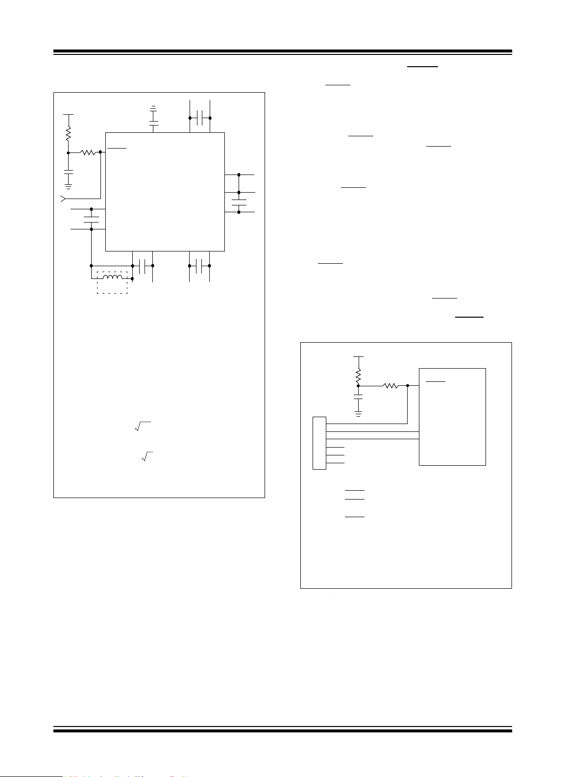
FIGURE 1-1: BLOCK DIAGRAM
This document contains device-specific information for
PIC32MX1XX/2XX 28/36/44-pin Family of devices.
Figure 1-1 illustrates a general block diagram of the
core and peripheral modules in the PIC32MX1XX/2XX
28/36/44-pin Family of devices.
Table 1-1 lists the functions of the various pins shown
in the pinout diagrams.
2011-2019 Microchip Technology Inc. DS60001168L-page 19

PIC32MX1XX/2XX 28/36/44-PIN FAMILY
TABLE 1-1: PINOUT I/O DESCRIPTIONS
Pin Number
(1)
(2)
28-pin
SSOP/
SPDIP/
SOIC
(2)
23
36-pin
VTLA
26
11
Pin Name
AN0 27 2 33 19
AN1 28 3 34 20 I Analog
AN2 1 4 35 21 I Analog
AN3 2 5 36 22 I Analog
AN4 3 6 1 23 I Analog
AN5 4 7 2 24 I Analog
AN6 — — 3 25 I Analog
AN7 — — 4 26 I Analog
AN8 — — — 27 I Analog
AN9 23262915IAnalog
AN10 22 25 28 14 I Analog
AN11 21 24 27 11 I Analog
AN12 20
CLKI 6 9 7 30 I ST/CMOS External clock source input. Always
CLKO 7 10 8 31 O — Oscillator crystal output. Connects to
OSC1 6 9 7 30 I ST/CMOS Oscillator crystal input. ST buffer when
OSC2 7 10 8 31 O — Oscillator crystal output. Connects to
SOSCI 8 11 9 33 I ST/CMOS 32.768 kHz low-power oscillator crystal
SOSCO 9 12 10 34 O — 32.768 kHz low-power oscillator crystal
REFCLKI PPS PPS PPS PPS I ST Reference Input Clock
REFCLKO PPS PPS PPS PPS O — Reference Output Clock
IC1 PPS PPS PPS PPS I ST Capture Inputs 1-5
IC2 PPS PPS PPS PPS I ST
IC3 PPS PPS PPS PPS I ST
IC4 PPS PPS PPS PPS I ST
IC5 PPS PPS PPS PPS I ST
Legend: CMOS = CMOS compatible input or output Analog = Analog input P = Power
Note 1: Pin numbers are provided for reference only. See the “Pin Diagrams” section for device pin availability.
28-pin
QFN
ST = Schmitt Trigger input with CMOS levels O = Output I = Input
TTL = TTL input buffer PPS = Peripheral Pin Select — = N/A
2: Pin number for PIC32MX1XX devices only.
3: Pin number for PIC32MX2XX devices only.
(2)
(3)
44-pin
QFN/
TQFP/
VTLA
(2)
10
(3)
36
Pin
Typ e
Buffer
Type
I Analog Analog input channels.
IAnalog
associated with OSC1 pin function.
crystal or resonator in Crystal Oscillator
mode. Optionally functions as CLKO in
RC and EC modes. Always associated
with OSC2 pin function.
configured in RC mode; CMOS
otherwise.
crystal or resonator in Crystal Oscillator
mode. Optionally functions as CLKO in
RC and EC modes.
input; CMOS otherwise.
output.
Description
DS60001168L-page 20 2011-2019 Microchip Technology Inc.

PIC32MX1XX/2XX 28/36/44-PIN FAMILY
TABLE 1-1: PINOUT I/O DESCRIPTIONS (CONTINUED)
Pin Number
(1)
Pin Name
28-pin
QFN
28-pin
SSOP/
SPDIP/
SOIC
36-pin
VTLA
44-pin
QFN/
TQFP/
VTLA
Pin
Typ e
Buffer
Type
Description
OC1 PPS PPS PPS PPS O — Output Compare Output 1
OC2 PPS PPS PPS PPS O — Output Compare Output 2
OC3 PPS PPS PPS PPS O — Output Compare Output 3
OC4 PPS PPS PPS PPS O — Output Compare Output 4
OC5 PPS PPS PPS PPS O — Output Compare Output 5
OCFA PPS PPS PPS PPS I ST Output Compare Fault A Input
OCFB PPS PPS PPS PPS I ST Output Compare Fault B Input
INT0 13 16 17 43 I ST External Interrupt 0
INT1 PPS PPS PPS PPS I ST External Interrupt 1
INT2 PPS PPS PPS PPS I ST External Interrupt 2
INT3 PPS PPS PPS PPS I ST External Interrupt 3
INT4 PPS PPS PPS PPS I ST External Interrupt 4
RA0 27 2 33 19
I/O ST PORTA is a bidirectional I/O port
RA1 28 3 34 20 I/O ST
RA2 6 9 7 30 I/O ST
RA3 710831I/OST
RA4 9 12 10 34 I/O ST
RA7 — — — 13 I/O ST
RA8 — — — 32 I/O ST
RA9 — — — 35 I/O ST
RA10 — — — 12 I/O ST
RB0 1 4 35 21 I/O ST PORTB is a bidirectional I/O port
RB1 2 5 36 22 I/O ST
RB2 3 6 1 23 I/O ST
RB3 4 7 2 24 I/O ST
RB4 8 11 9 33 I/O ST
RB5 11141541I/OST
RB6 12
(2)
15
(2)
16
(2)
42
(2)
I/O ST
RB7 13161743I/OST
RB8 14171844I/OST
RB9 15 18 19 1 I/O ST
RB10 18 21 24 8 I/O ST
RB11 19 22 25 9 I/O ST
RB12 20
(2)
23
(2)
26
(2)
10
(2)
I/O ST
RB13 21 24 27 11 I/O ST
RB14 22 25 28 14 I/O ST
RB15 23 26 29 15 I/O ST
Legend: CMOS = CMOS compatible input or output Analog = Analog input P = Power
ST = Schmitt Trigger input with CMOS levels O = Output I = Input
TTL = TTL input buffer PPS = Peripheral Pin Select — = N/A
Note 1: Pin numbers are provided for reference only. See the “Pin Diagrams” section for device pin availability.
2: Pin number for PIC32MX1XX devices only.
3: Pin number for PIC32MX2XX devices only.
2011-2019 Microchip Technology Inc. DS60001168L-page 21

PIC32MX1XX/2XX 28/36/44-PIN FAMILY
TABLE 1-1: PINOUT I/O DESCRIPTIONS (CONTINUED)
Pin Number
(1)
Pin Name
RC0 — — 3 25 I/O ST PORTC is a bidirectional I/O port
RC1 — — 4 26 I/O ST
RC2 — — — 27 I/O ST
RC3 — — 11 36 I/O ST
RC4 — — — 37 I/O ST
RC5 — — — 38 I/O ST
RC6 — — — 2 I/O ST
RC7 — — — 3 I/O ST
RC8 — — — 4 I/O ST
RC9 — — 20 5 I/O ST
T1CK 9 12 10 34 I ST Timer1 external clock input
T2CK PPS PPS PPS PPS I ST Timer2 external clock input
T3CK PPS PPS PPS PPS I ST Timer3 external clock input
T4CK PPS PPS PPS PPS I ST Timer4 external clock input
T5CK PPS PPS PPS PPS I ST Timer5 external clock input
U1CTS
U1RTS
U1RX PPS PPS PPS PPS I ST
U1TX PPS PPS PPS PPS
U2CTS
U2RTS
U2RX PPS PPS PPS PPS
U2TX PPS PPS PPS PPS
SCK1 22 25 28 14
SDI1 PPS PPS PPS PPS
SDO1 PPS PPS PPS PPS
SS1
SCK2 23 26 29 15 I/O ST Synchronous serial clock input/output for
SDI2 PPS PPS PPS PPS
SDO2 PPS PPS PPS PPS
SS2
SCL1 14 17 18 44 I/O ST Synchronous serial clock input/output for
Legend: CMOS = CMOS compatible input or output Analog = Analog input P = Power
Note 1: Pin numbers are provided for reference only. See the “Pin Diagrams” section for device pin availability.
28-pin
QFN
PPS PPS PPS PPS I ST UART1 clear to send
PPS PPS PPS PPS O — UART1 ready to send
PPS PPS PPS PPS I ST UART2 clear to send
PPS PPS PPS PPS O — UART2 ready to send
PPS PPS PPS PPS I/O ST SPI1 slave synchronization or frame
PPS PPS PPS PPS I/O ST SPI2 slave synchronization or frame
ST = Schmitt Trigger input with CMOS levels O = Output I = Input
TTL = TTL input buffer PPS = Peripheral Pin Select — = N/A
2: Pin number for PIC32MX1XX devices only.
3: Pin number for PIC32MX2XX devices only.
28-pin
SSOP/
SPDIP/
SOIC
36-pin
VTLA
44-pin
QFN/
TQFP/
VTLA
Pin
Typ e
I/O ST
Buffer
Type
UART1 receive
O — UART1 transmit
IST
O—
IST
O—
IST
O—
UART2 receive
UART2 transmit
Synchronous serial clock input/output for
SPI1
SPI1 data in
SPI1 data out
pulse I/O
SPI2
SPI2 data in
SPI2 data out
pulse I/O
I2C1
Description
DS60001168L-page 22 2011-2019 Microchip Technology Inc.

PIC32MX1XX/2XX 28/36/44-PIN FAMILY
TABLE 1-1: PINOUT I/O DESCRIPTIONS (CONTINUED)
Pin Number
(1)
Pin Name
28-pin
QFN
28-pin
SSOP/
SPDIP/
SOIC
36-pin
VTLA
44-pin
QFN/
TQFP/
VTLA
Pin
Typ e
Buffer
Type
Description
SDA1 15 18 19 1 I/O ST Synchronous serial data input/output for
I2C1
SCL2 4 7 2 24 I/O ST Synchronous serial clock input/output for
I2C2
SDA2 3 6 1 23 I/O ST Synchronous serial data input/output for
I2C2
TMS
19
11
(2)
(3)
22
14
(2)
(3)
25
15
(2)
(3)
12 I ST JTAG Test mode select pin
TCK 14 17 18 13 I ST JTAG test clock input pin
TDI 13 16 17 35 O — JTAG test data input pin
TDO 15 18 19 32 O — JTAG test data output pin
RTCC 4 7 2 24 O ST Real-Time Clock alarm output
C
VREF
- 28 3 34 20 I Analog
VREF
+ 27 2 33 19 I Analog Comparator Voltage Reference (high)
C
C
VREFOUT
C1INA 4 7 2 24
22 25 28 14 O Analog Comparator Voltage Reference output
I Analog Comparator Inputs
Comparator Voltage Reference (low)
C1INB 3 6 1 23 I Analog
C1INC 2 5 36 22 I Analog
C1IND 1 4 35 21 I Analog
C2INA 2 5 36 22 I Analog
C2INB 1 4 35 21 I Analog
C2INC 4 7 2 24 I Analog
C2IND 3 6 1 23 I Analog
C3INA 23 262915IAnalog
C3INB 22 252814IAnalog
C3INC 27 2 33 19 I Analog
C3IND 1 4 35 21 I Analog
C1OUT PPS PPS PPS PPS O — Comparator Outputs
C2OUT PPS PPS PPS PPS O —
C3OUT PPS PPS PPS PPS O —
Legend: CMOS = CMOS compatible input or output Analog = Analog input P = Power
ST = Schmitt Trigger input with CMOS levels O = Output I = Input
TTL = TTL input buffer PPS = Peripheral Pin Select — = N/A
Note 1: Pin numbers are provided for reference only. See the “Pin Diagrams” section for device pin availability.
2: Pin number for PIC32MX1XX devices only.
3: Pin number for PIC32MX2XX devices only.
2011-2019 Microchip Technology Inc. DS60001168L-page 23

PIC32MX1XX/2XX 28/36/44-PIN FAMILY
TABLE 1-1: PINOUT I/O DESCRIPTIONS (CONTINUED)
Pin Number
(1)
Pin Name
28-pin
QFN
28-pin
SSOP/
SPDIP/
SOIC
36-pin
VTLA
44-pin
QFN/
TQFP/
VTLA
Pin
Typ e
Buffer
Type
Description
PMA0 7 10 8 3 I/O TTL/ST Parallel Master Port Address bit 0 input
(Buffered Slave modes) and output
(Master modes)
PMA1 9 12 10 2 I/O TTL/ST Parallel Master Port Address bit 1 input
(Buffered Slave modes) and output
(Master modes)
PMA2 — — 27 O — Parallel Master Port address
PMA3 — — 38 O —
(Demultiplexed Master modes)
PMA4 — — 37 O —
PMA5 — — 4 O —
PMA6 — — 5 O —
PMA7 — — 13 O —
PMA8 — — 32 O —
PMA9 — — 35 O —
PMA10 — — 12 O —
PMCS1 23 26 29 15 O — Parallel Master Port Chip Select 1 strobe
(2)
PMD0
PMD1
PMD2
20
19
18
(3)
1
(2)
(3)
2
(2)
(3)
3
PMD3 15 18 19 1
23
22
21
(2)
(3)
4
(2)
(3)
5
(2)
(3)
6
26
35
25
36
24
(2)
(3)
(2)
(3)
(2)
(3)
1
10
21
22
23
(2)
(3)
(2)
9
(3)
(2)
8
(3)
I/O TTL/ST
I/O TTL/ST
I/O TTL/ST
Parallel Master Port data (Demultiplexed
Master mode) or address/data
(Multiplexed Master modes)
I/O TTL/ST
PMD4 14 17 18 44 I/O TTL/ST
PMD5 13 16 17 43 I/O TTL/ST
PMD6 12
28
PMD7 11
27
(2)
(3)
(2)
(3)
15
14
(2)
(3)
3
(2)
(3)
2
16
34
15
33
(2)
(3)
(2)
(3)
42
20
41
19
(2)
(3)
(2)
(3)
I/O TTL/ST
I/O TTL/ST
PMRD 21 24 27 11 O — Parallel Master Port read strobe
PMWR
V
BUS
V
USB3V
V
BUSON
(2)
22
(3)
4
(3)
12
20
22
(3)
(3)
3
25
15
23
25
(2)
(3)
7
(3)
(3)
(3)
28
16
26
28
(2)
(3)
2
(3)
(3)
(3)
14
24
42
10
14
(2)
(3)
(3)
(3)
(3)
O — Parallel Master Port write strobe
I Analog USB bus power monitor
P — USB internal transceiver supply. This pin
DD
must be connected to V
.
O — USB Host and OTG bus power control
output
D+ 18
D- 19
(3)
(3)
21
22
(3)
(3)
24
25
(3)
(3)
(3)
8
(3)
9
I/O Analog USB D+
I/O Analog USB D-
Legend: CMOS = CMOS compatible input or output Analog = Analog input P = Power
ST = Schmitt Trigger input with CMOS levels O = Output I = Input
TTL = TTL input buffer PPS = Peripheral Pin Select — = N/A
Note 1: Pin numbers are provided for reference only. See the “Pin Diagrams” section for device pin availability.
2: Pin number for PIC32MX1XX devices only.
3: Pin number for PIC32MX2XX devices only.
DS60001168L-page 24 2011-2019 Microchip Technology Inc.

PIC32MX1XX/2XX 28/36/44-PIN FAMILY
TABLE 1-1: PINOUT I/O DESCRIPTIONS (CONTINUED)
Pin Number
(1)
Pin Name
28-pin
QFN
USBID 11
(3)
28-pin
SSOP/
SPDIP/
SOIC
(3)
14
36-pin
VTLA
(3)
15
44-pin
QFN/
TQFP/
VTLA
(3)
41
Pin
Typ e
Buffer
Type
I ST USB OTG ID detect
Description
CTED1 27 2 33 19 I ST CTMU External Edge Input
CTED2 28 3 34 20 I ST
CTED313161743IST
CTED4 15 18 19 1 I ST
CTED522252814IST
CTED623262915IST
CTED7 — — 20 5 I ST
CTED8 — — — 13 I ST
CTED9 9 12 10 34 I ST
CTED10 14 17 18 44 I ST
CTED11 18 21 24 8 I ST
CTED12 2 5 36 22 I ST
CTED13 3 6 1 23 I ST
CTPLS 21 24 27 11 O — CTMU Pulse Output
PGED1 1 4 35 21 I/O ST Data I/O pin for Programming/Debugging
Communication Channel 1
PGEC1 2 5 36 22 I ST Clock input pin for
Programming/Debugging
Communication Channel 1
PGED2 18 21 24 8 I/O ST Data I/O pin for Programming/Debugging
Communication Channel 2
PGEC2 19 22 25 9 I ST Clock input pin for
Programming/Debugging
Communication Channel 2
(2)
PGED3
PGEC3
11
27
12
28
(3)
(2)
(3)
PGED4 — — 3 12
PGEC4 — — 4 13
14
15
(2)
(3)
2
(2)
(3)
3
15
33
16
34
(2)
(3)
(2)
(3)
41
19
42
20
(2)
(3)
(2)
(3)
I/O ST
IST
I/O ST
IST
Data I/O pin for Programming/Debugging
Communication Channel 3
Clock input pin for Programming/
Debugging Communication Channel 3
Data I/O pin for Programming/Debugging
Communication Channel 4
Clock input pin for Programming/
Debugging Communication Channel 4
Legend: CMOS = CMOS compatible input or output Analog = Analog input P = Power
ST = Schmitt Trigger input with CMOS levels O = Output I = Input
TTL = TTL input buffer PPS = Peripheral Pin Select — = N/A
Note 1: Pin numbers are provided for reference only. See the “Pin Diagrams” section for device pin availability.
2: Pin number for PIC32MX1XX devices only.
3: Pin number for PIC32MX2XX devices only.
2011-2019 Microchip Technology Inc. DS60001168L-page 25

PIC32MX1XX/2XX 28/36/44-PIN FAMILY
TABLE 1-1: PINOUT I/O DESCRIPTIONS (CONTINUED)
Pin Number
(1)
Pin Name
28-pin
QFN
28-pin
SSOP/
SPDIP/
SOIC
36-pin
VTLA
44-pin
QFN/
TQFP/
VTLA
Pin
Typ e
Buffer
Type
Description
MCLR 26 1 32 18 I/P ST Master Clear (Reset) input. This pin is an
active-low Reset to the device.
AV
DD
25 28 31 17 P — Positive supply for analog modules. This
pin must be connected at all times.
AV
V
SS
DD
24 27 30 16 P — Ground reference for analog modules
10 13 5, 13, 14, 2328, 40 P — Positive supply for peripheral logic and
I/O pins
V
V
CAP
SS
17 20 22 7 P — CPU logic filter capacitor connection
5, 16 8, 19 6, 12, 21 6, 29, 39 P — Ground reference for logic and I/O pins.
This pin must be connected at all times.
V
REF
+ 27 2 33 19 I Analog Analog voltage reference (high) input
V
REF
- 28 3 34 20 I Analog Analog voltage reference (low) input
Legend: CMOS = CMOS compatible input or output Analog = Analog input P = Power
ST = Schmitt Trigger input with CMOS levels O = Output I = Input
TTL = TTL input buffer PPS = Peripheral Pin Select — = N/A
Note 1: Pin numbers are provided for reference only. See the “Pin Diagrams” section for device pin availability.
2: Pin number for PIC32MX1XX devices only.
3: Pin number for PIC32MX2XX devices only.
DS60001168L-page 26 2011-2019 Microchip Technology Inc.

PIC32MX1XX/2XX 28/36/44-PIN FAMILY
2.0 GUIDELINES FOR GETTING STARTED WITH 32-BIT MCUs
Note: This data sheet summarizes the features
of the PIC32MX1XX/2XX 28/36/44-pin
Family of devices. It is not intended to be
a comprehensive reference source. To
complement the information in this data
sheet, refer to the documents listed in the
Documentation > Reference Manual
section of the Microchip PIC32 web site
(www.microchip.com/pic32).
2.1 Basic Connection Requirements
Getting started with the PIC32MX1XX/2XX 28/36/44pin Family of 32-bit Microcontrollers (MCUs) requires
attention to a minimal set of device pin connections
before proceeding with development. The following is a
list of pin names, which must always be connected:
DD
•All V
•All AV
•V
•MCLR pin (see 2.4 “Master Clear (MCLR) Pin”)
• PGECx/PGEDx pins, used for In-Circuit Serial
• OSC1 and OSC2 pins, when external oscillator
The following pins may be required:
•V
and VSS pins (see 2.2 “Decoupling
Capacitors”)
DD
and AVSS pins, even if the ADC module
is not used (see 2.2 “Decoupling Capacitors”)
CAP
pin (see 2.3 “Capacitor on Internal
CAP
Voltage Regulator (V
Programming™ (ICSP™) and debugging purposes (see 2.5 “ICSP Pins”)
source is used (see 2.7 “External Oscillator
Pins”)
REF
+/V
REF
- pins – used when external voltage
reference for the ADC module is implemented
Note: The AV
nected, regardless of ADC use and the
ADC voltage reference source.
DD
)”)
and AVSS pins must be con-
2.2 Decoupling Capacitors
The use of decoupling capacitors on power supply
pins, such as V
See Figure 2-1.
Consider the following criteria when using decoupling
capacitors:
• Value and type of capacitor: A value of 0.1 µF
(100 nF), 10-20V is recommended. The capacitor
should be a low Equivalent Series Resistance
(low-ESR) capacitor and have resonance frequency in the range of 20 MHz and higher. It is
further recommended that ceramic capacitors be
used.
• Placement on the printed circuit board: The
decoupling capacitors should be placed as close
to the pins as possible. It is recommended that
the capacitors be placed on the same side of the
board as the device. If space is constricted, the
capacitor can be placed on another layer on the
PCB using a via; however, ensure that the trace
length from the pin to the capacitor is within onequarter inch (6 mm) in length.
• Handling high frequency noise: If the board is
experiencing high frequency noise, upward of
tens of MHz, add a second ceramic-type capacitor
in parallel to the above described decoupling
capacitor. The value of the second capacitor can
be in the range of 0.01 µF to 0.001 µF. Place this
second capacitor next to the primary decoupling
capacitor. In high-speed circuit designs, consider
implementing a decade pair of capacitances as
close to the power and ground pins as possible.
For example, 0.1 µF in parallel with 0.001 µF.
• Maximizing performance: On the board layout
from the power supply circuit, run the power and
return traces to the decoupling capacitors first,
and then to the device pins. This ensures that the
decoupling capacitors are first in the power chain.
Equally important is to keep the trace length
between the capacitor and the power pins to a
minimum thereby reducing PCB track inductance.
DD
, VSS, AVDD and AVSS is required.
2011-2019 Microchip Technology Inc. DS60001168L-page 27
PIC32MX1XX/2XX 28/36/44-PIN FAMILY
PIC32
V
DD
V
SS
V
DD
V
SS
V
SS
V
DD
AVDDAV
SS
VDDV
SS
0.1 µF
Ceramic
0.1 µF
Ceramic
0.1 µF
Ceramic
0.1 µF
Ceramic
C
10K
V
DD
MCLR
0.1 µF
Ceramic
L1
(2)
R1
Note 1: If the USB module is not used, this pin must be
connected to V
DD
.
2: As an option, instead of a hard-wired connection, an
inductor (L1) can be substituted between V
DD
and
AV
DD
to improve ADC noise rejection. The inductor
impedance should be less than 3 and the inductor
capacity greater than 10 mA.
Where:
f
F
CNV
2
------------ --
=
f
1
2 LC
------------ -----------
=
L
1
2fC
------------ ----------
2
=
(i.e., ADC conversion rate/2)
Connect
(2)
V
USB3V
3
(1)
V
CAP
Tantalum or
ceramic 10 µF
ESR 3
(3)
1: Aluminum or electrolytic capacitors should not be
used. ESR 3 from -40ºC to 125ºC @ SYSCLK
frequency (i.e., MIPS).
1K
0.1 µF
Note 1: 470R1 1 will limit any current flowing into
MCLR
from the external capacitor C, in the event of
MCLR
pin breakdown, due to Electrostatic Discharge
(ESD) or Electrical Overstress (EOS). Ensure that the
MCLR
pin VIH and VIL specifications are met without
interfering with the Debug/Programmer tools.
2: The capacitor can be sized to prevent unintentional
Resets from brief glitches or to extend the device
Reset period during POR.
3: No pull-ups or bypass capacitors are allowed on
active debug/program PGECx/PGEDx pins.
R1
(1)
10k
V
DD
MCLR
PIC32
1 k
0.1 µF
(2)
PGECx
(3)
PGEDx
(3)
ICSP™
1
5
4
2
3
6
V
DD
V
SS
NC
R
C
FIGURE 2-1: RECOMMENDED
MINIMUM CONNECTION
2.4 Master Clear (MCLR) Pin
The MCLR pin provides two specific device
functions:
• Device Reset
• Device programming and debugging
Pulling The MCLR
Figure 2-2 illustrates a typical MCLR circuit. During
device programming and debugging, the resistance
and capacitance that can be added to the pin must
be considered. Device programmers and debuggers
drive the MCLR
levels (V
IH
and VIL) and fast signal transitions must
not be adversely affected. Therefore, specific values
of R and C will need to be adjusted based on the
application and PCB requirements.
For example, as illustrated in Figure 2-2, it is
recommended that the capacitor C, be isolated from
the MCLR
pin during programming and debugging
operations.
Place the components illustrated in Figure 2-2 within
one-quarter inch (6 mm) from the MCLR
FIGURE 2-2: EXAMPLE OF MCLR PIN
pin low generates a device Reset.
pin. Consequently, specific voltage
pin.
CONNECTIONS
2.2.1 BULK CAPACITORS
The use of a bulk capacitor is recommended to improve
power supply stability. Typical values range from 4.7 µF
to 47 µF. This capacitor should be located as close to
the device as possible.
2.3 Capacitor on Internal Voltage
2.3.1 INTERNAL REGULATOR MODE
A low-ESR (3 ohm) capacitor is required on the V
pin, which is used to stabilize the internal voltage
regulator output. The V
to VDD, and must have a C
6V rating, connected to ground. The type can be
ceramic or tantalum. Refer to 30.0 “Electrical
Characteristics” for additional information on C
specifications.
DS60001168L-page 28 2011-2019 Microchip Technology Inc.
Regulator (V
CAP
)
CAP
pin must not be connected
EFC
capacitor, with at least a
CAP
EFC
2.5 ICSP Pins
The PGECx and PGEDx pins are used for ICSP and
debugging purposes. It is recommended to keep the
trace length between the ICSP connector and the ICSP
pins on the device as short as possible. If the ICSP connector is expected to experience an ESD event, a
series resistor is recommended, with the value in the
range of a few tens of Ohms, not to exceed 100 Ohms.

PIC32MX1XX/2XX 28/36/44-PIN FAMILY
Main Oscillator
Guard Ring
Guard Trace
Secondary
Oscillator
Pull-up resistors, series diodes and capacitors on the
PGECx and PGEDx pins are not recommended as they
will interfere with the programmer/debugger communications to the device. If such discrete components are
an application requirement, they should be removed
from the circuit during programming and debugging.
Alternatively, refer to the AC/DC characteristics and
timing requirements information in the respective
device Flash programming specification for information
on capacitive loading limits and pin input voltage high
IH
) and input low (VIL) requirements.
(V
Ensure that the “Communication Channel Select” (i.e.,
PGECx/PGEDx pins) programmed into the device
matches the physical connections for the ICSP to
MPLAB
®
ICD 3 or MPLAB REAL ICE™.
For more information on ICD 3 and REAL ICE
connection requirements, refer to the following
documents that are available on the Microchip web
site:
®
• “Using MPLAB
ICD 3” (poster) (DS50001765)
• “MPLAB® ICD 3 Design Advisory” (DS50001764)
• “MPLAB® REAL ICE™ In-Circuit Debugger
User’s Guide” (DS50001616)
®
• “Using MPLAB
REAL ICE™ Emulator” (poster)
(DS50001749)
The oscillator circuit should be placed on the same side
of the board as the device. Also, place the oscillator circuit close to the respective oscillator pins, not exceeding one-half inch (12 mm) distance between them. The
load capacitors should be placed next to the oscillator
itself, on the same side of the board. Use a grounded
copper pour around the oscillator circuit to isolate them
from surrounding circuits. The grounded copper pour
should be routed directly to the MCU ground. Do not
run any signal traces or power traces inside the ground
pour. Also, if using a two-sided board, avoid any traces
on the other side of the board where the crystal is
placed. A suggested layout is illustrated in Figure 2-3.
FIGURE 2-3: SUGGESTED OSCILLATOR
CIRCUIT PLACEMENT
2.6 JTAG
The TMS, TDO, TDI and TCK pins are used for testing
and debugging according to the Joint Test Action
Group (JTAG) standard. It is recommended to keep the
trace length between the JTAG connector and the
JTAG pins on the device as short as possible. If the
JTAG connector is expected to experience an ESD
event, a series resistor is recommended with the value
in the range of a few tens of Ohms, not to exceed 100
Ohms.
Pull-up resistors, series diodes and capacitors on the
TMS, TDO, TDI and TCK pins are not recommended
as they will interfere with the programmer/debugger
communications to the device. If such discrete components are an application requirement, they should be
removed from the circuit during programming and
debugging. Alternatively, refer to the AC/DC characteristics and timing requirements information in the
respective device Flash programming specification for
information on capacitive loading limits and pin input
IH
voltage high (V
) and input low (VIL) requirements.
2.7 External Oscillator Pins
Many MCUs have options for at least two oscillators: a
high-frequency primary oscillator and a low-frequency
secondary oscillator (refer to Section 8.0 “Oscillator
Configuration” for details).
2.8 Unused I/Os
Unused I/O pins should not be allowed to float as
inputs. They can be configured as outputs and driven
to a logic-low state.
Alternatively, inputs can be reserved by connecting the
SS
pin to V
the pin as an input.
through a 1k to 10k resistor and configuring
2011-2019 Microchip Technology Inc. DS60001168L-page 29

PIC32MX1XX/2XX 28/36/44-PIN FAMILY
Crystal manufacturer recommended: C1 = C2 = 15 pF
Therefore:
C
LOAD
= {( [CIN + C1] * [C
OUT
+ C2] ) / [CIN + C1 + C2 + C
OUT
]}
+ estimated oscillator PCB stray capacitance
= {( [5 + 15][5 + 15] ) / [5 + 15 + 15 + 5] } + 2.5 pF
= {( [20][20]) / [40] } + 2.5
= 10 + 2.5 = 12.5 pF
Rounded to the nearest standard value or 12 pF in this example for
Primary Oscillator crystals “C1” and “C2”.
OSC2 OSC1
1M
Typ ical XT
(4-10 MHz)
Circuit A
C1
C2
OSC2 OSC1
Typ ical HS
(10-25 MHz)
Circuit B
C1
C2
Rs
OSC2
OSC1
1M
Typic al XT/ HS
(4-25 MHz)
Circuit C
C1
C2
1M
Rs
OSC2
OSC1
Not Recommended
Circuit D
Not Recommended
1M
Rs
OSC2 OSC1
Circuit E
2.8.1 CRYSTAL OSCILLATOR DESIGN
CONSIDERATION
The following example assumptions are used to
calculate the Primary Oscillator loading capacitor
values:
IN
= PIC32_OSC2_Pin Capacitance = ~4-5 pF
•C
OUT
•C
= PIC32_OSC1_Pin Capacitance = ~4-5 pF
• C1 and C2 = XTAL manufacturing recommended
loading capacitance
• Estimated PCB stray capacitance, (i.e.,12 mm
length) = 2.5 pF
EXAMPLE 2-1: CRYSTAL LOAD CAPACITOR
CALCULATION
The following tips are used to increase oscillator gain,
(i.e., to increase peak-to-peak oscillator signal):
• Select a crystal with a lower “minimum” power drive
rating
• Select an crystal oscillator with a lower XTAL
manufacturing “ESR” rating.
• Add a parallel resistor across the crystal. The smaller
the resistor value the greater the gain. It is recommended to stay in the range of 600k to 1M
• C1 and C2 values also affect the gain of the oscillator.
The lower the values, the higher the gain.
• C2/C1 ratio also affects gain. To increase the gain,
make C1 slightly smaller than C2, which will also help
start-up performance.
Note: Do not add excessive gain such that the
oscillator signal is clipped, flat on top of
the sine wave. If so, you need to reduce
the gain or add a series resistor, RS, as
shown in circuit “C” in Figure 2-4. Failure
to do so will stress and age the crystal,
which can result in an early failure. Adjust
the gain to trim the max peak-to-peak to
~V
DD
-0.6V. When measuring the oscilla-
tor signal you must use a FET scope
probe or a probe with 1.5 pF or the
scope probe itself will unduly change the
gain and peak-to-peak levels.
2.8.1.1 Additional Microchip References
• AN588 “PICmicro® Microcontroller Oscill ato r
• AN826 “Crystal Oscillator Basics and Crystal
• AN849 “Basic PICmicro® Oscillator Design”
DS60001168L-page 30 2011-2019 Microchip Technology Inc.
Design Guide”
Selection for rfPIC™ and PICmicro
®
FIGURE 2-4: PRIMARY CRYSTAL
OSCILLATOR CIRCUIT
RECOMMENDATIONS
Devices”
 Loading...