

Datasheet PIC32MX110F016B, PIC32MX110F016C, PIC32MX110F016D, PIC32MX120F032B, PIC32MX120F032C Datasheet
...
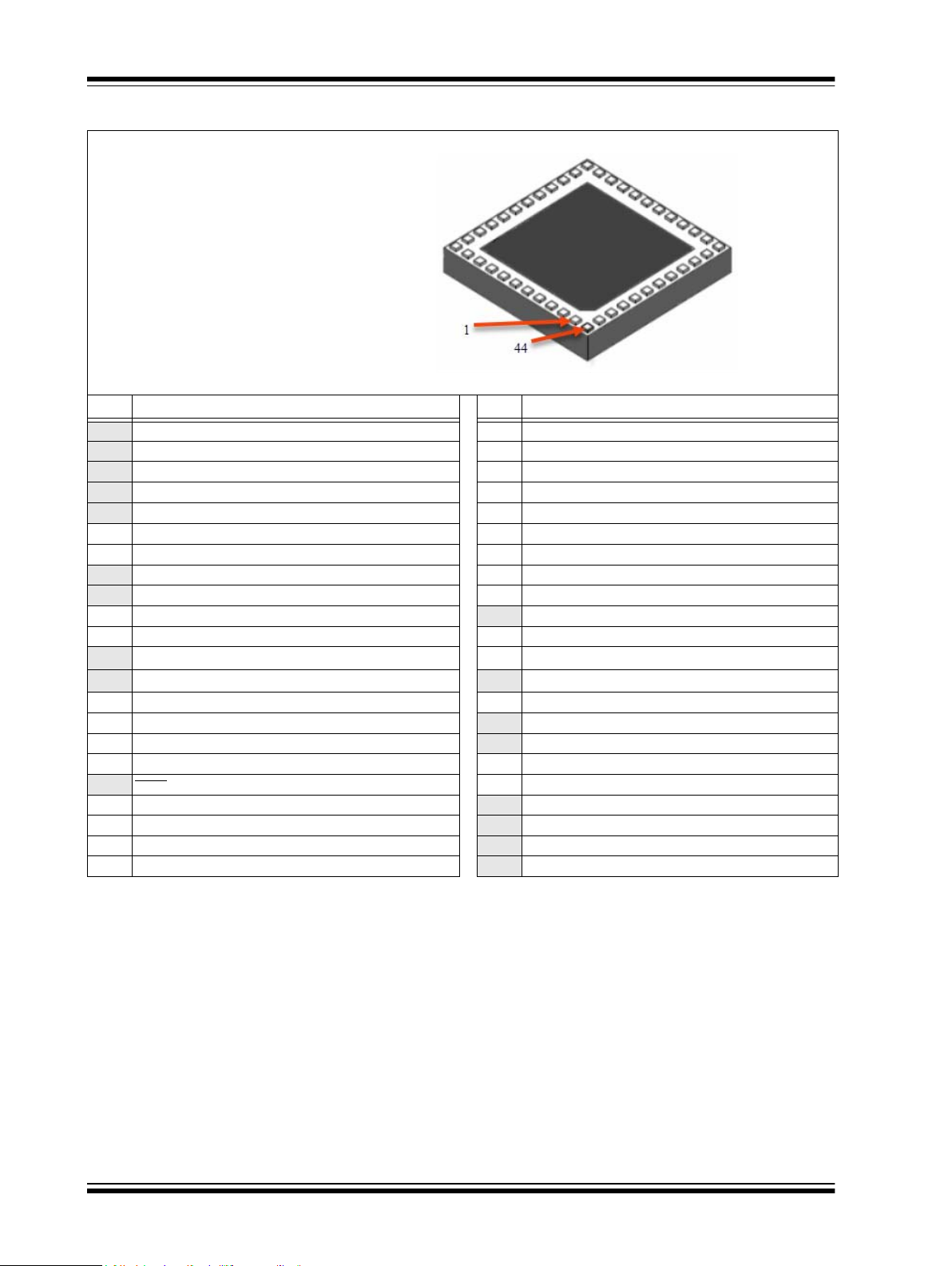
PIC32MX1XX/2XX 28/36/44-PIN
32-bit Microcontrollers (up to 256 KB Flash and 64 KB SRAM) with
Audio and Graphics Interfaces, USB, and Advanced Analog
Operating Conditions
• 2.3V to 3.6V, -40ºC to +105ºC, DC to 40 MHz
• 2.3V to 3.6V, -40ºC to +85ºC, DC to 50 MHz
Core: 50 MHz/83 DMIPS MIPS32® M4K
•MIPS16e® mode for up to 40% smaller code size
• Code-efficient (C and Assembly) architecture
• Single-cycle (MAC) 32x16 and two-cycle 32x32 multiply
®
Clock Management
• 0.9% internal oscillator
• Programmable PLLs and oscillator clock sources
• Fail-Safe Clock Monitor (FSCM)
• Independent Watchdog Timer
• Fast wake-up and start-up
Power Management
• Low-power management modes (Sleep and Idle)
• Integrated Power-on Reset and Brown-out Reset
• 0.5 mA/MHz dynamic current (typical)
PD
•44 μA I
current (typical)
Audio Interface Features
• Data communication: I2S, LJ, RJ, and DSP modes
• Control interface: SPI and I
• Master clock:
- Generation of fractional clock frequencies
- Can be synchronized with USB clock
- Can be tuned in run-time
2
C
Advanced Analog Features
• ADC Module:
- 10-bit 1.1 Msps rate with one S&H
- Up to 10 analog inputs on 28-pin devices and 13
analog inputs on 44-pin devices
• Flexible and independent ADC trigger sources
• Charge Time Measurement Unit (CTMU):
- Supports mTouch™ capacitive touch sensing
- Provides high-resolution time measurement (1 ns)
- On-chip temperature measurement capability
• Comparators:
- Up to three Analog Comparator modules
- Programmable references with 32 voltage points
Timers/Output Compare/Input Capture
• Five General Purpose Timers:
- Five 16-bit and up to two 32-bit Timers/Counters
• Five Output Compare (OC) modules
• Five Input Capture (IC) modules
• Peripheral Pin Select (PPS) to allow function remap
• Real-Time Clock and Calendar (RTCC) module
Communication Interfaces
• USB 2.0-compliant Full-speed OTG controller
• Two UART modules (12.5 Mbps):
- Supports LIN 2.0 protocols and IrDA
• Two 4-wire SPI modules (25 Mbps)
2
•Two I
• PPS to allow function remap
• Parallel Master Port (PMP)
C modules (up to 1 Mbaud) with SMBus support
®
support
Direct Memory Access (DMA)
• Four channels of hardware DMA with automatic data
size detection
• Two additional channels dedicated for USB
• Programmable Cyclic Redundancy Check (CRC)
Input/Output
• 10 mA source/sink on all I/O pins and up to 14 mA on
non-standard V
• 5V-tolerant pins
• Selectable open drain, pull-ups, and pull-downs
• External interrupts on all I/O pins
OH
Class B Support
• Class B Safety Library, IEC 60730
Debugger Development Support
• In-circuit and in-application programming
•4-wire MIPS
• Unlimited program and six complex data breakpoints
• IEEE 1149.2-compatible (JTAG) boundary scan
®
Enhanced JTAG interface
Packages
Type SOIC SSOP SPDIP QFN VTLA TQFP
Pin Count 28 28 28 28 44 36 44 44
I/O Pins (up to) 21 21 21 21 34 25 34 34
Contact/Lead Pitch 1.27 0.65 0.100'' 0.65 0.65 0.50 0.50 0.80
Dimensions 17.90x7.50x2.65 10.2x5.3x2 1.365''x.285''x.135'' 6x6x0.9 8x8x0.9 5x5x0.9 6x6x0.9 10x10x1
Note: All dimensions are in millimeters (mm) unless specified.
2011-2019 Microchip Technology Inc. DS60001168L-page 1

PIC32MX1XX/2XX 28/36/44-PIN FAMILY
TABLE 1: PIC32MX1XX 28/36/44-PIN GENERAL PURPOSE FAMILY FEATURES
Remappable Peripherals
(1)
(3)
S
UART
2
SPI/I
Analog Comparators
External Interrupts
Device
PIC32MX110F016B 28 16+3 4 20 5/5/5 2 2 5 3 N 2 Y 4/0 Y 10 Y 21 Y
PIC32MX110F016C 36 16+3 4 24 5/5/5 2 2 5 3 N 2 Y 4/0 Y 12 Y 25 Y VTLA
PIC32MX110F016D 44 16+3 4 32 5/5/5 2 2 5 3 N 2 Y 4/0 Y 13 Y 35 Y
PIC32MX120F032B 28 32+3 8 20 5/5/5 2 2 5 3 N 2 Y 4/0 Y 10 Y 21 Y
PIC32MX120F032C 36 32+3 8 24 5/5/5 2 2 5 3 N 2 Y 4/0 Y 12 Y 25 Y VTLA
PIC32MX120F032D 44 32+3 8 32 5/5/5 2 2 5 3 N 2 Y 4/0 Y 13 Y 35 Y
PIC32MX130F064B 28 64+3 16 20 5/5/5 2 2 5 3 N 2 Y 4/0 Y 10 Y 21 Y
PIC32MX130F064C 36 64+3 16 24 5/5/5 2 2 5 3 N 2 Y 4/0 Y 12 Y 25 Y VTLA
PIC32MX130F064D 44 64+3 16 32 5/5/5 2 2 5 3 N 2 Y 4/0 Y 13 Y 35 Y
PIC32MX150F128B 28 128+3 32 20 5/5/5 2 2 5 3 N 2 Y 4/0 Y 10 Y 21 Y
PIC32MX150F128C 36 128+3 32 24 5/5/5 2 2 5 3 N 2 Y 4/0 Y 12 Y 25 Y VTLA
PIC32MX150F128D 44 128+3 32 32 5/5/5 2 2 5 3 N 2 Y 4/0 Y 13 Y 35 Y
PIC32MX130F256B 28 256+3 16 20 5/5/5 2 2 5 3 N 2 Y 4/0 Y 10 Y 21 Y
PIC32MX130F256D 44 256+3 16 32 5/5/5 2 2 5 3 N 2 Y 4/0 Y 13 Y 35 Y
PIC32MX170F256B 28 256+3 64 20 5/5/5 2 2 5 3 N 2 Y 4/0 Y 10 Y 21 Y
PIC32MX170F256D 44 256+3 64 32 5/5/5 2 2 5 3 N 2 Y 4/0 Y 13 Y 35 Y
Note 1: This device features 3 KB of boot Flash memory.
2: Four out of five timers are remappable.
3: Four out of five external interrupts are remappable.
Pins
Program Memory (KB)
Data Memory (KB)
Remappable Pins
/Capture/Compare
(2)
Timers
C
2
I
PMP
USB On-The-Go (OTG)
CTMU
DMA Channels
(Programmable/Dedicated)
RTCC
10-bit 1 Msps ADC (Channels)
I/O Pins
JTAG
SOIC,
SSOP,
SPDIP,
QFN
VTLA,
TQFP,
QFN
SOIC,
SSOP,
SPDIP,
QFN
VTLA,
TQFP,
QFN
SOIC,
SSOP,
SPDIP,
QFN
VTLA,
TQFP,
QFN
SOIC,
SSOP,
SPDIP,
QFN
VTLA,
TQFP,
QFN
SSOP,
SPDIP,
QFN
VTLA,
TQFP,
QFN
SOIC,
SSOP,
SPDIP,
QFN
VTLA,
TQFP,
QFN
Packages
DS60001168L-page 2 2011-2019 Microchip Technology Inc.

PIC32MX1XX/2XX 28/36/44-PIN FAMILY
TABLE 2: PIC32MX2XX 28/36/44-PIN USB FAMILY FEATURES
Remappable Peripherals
(1)
(3)
S
Device
PIC32MX210F016B 28 16+3 4 19 5/5/5 2 2 5 3 Y 2 Y 4/2 Y 9 Y 19 Y
PIC32MX210F016C 36 16+3 4 23 5/5/5 2 2 5 3 Y 2 Y 4/2 Y 12 Y 25 Y VTLA
PIC32MX210F016D 44 16+3 4 31 5/5/5 2 2 5 3 Y 2 Y 4/2 Y 13 Y 33 Y
PIC32MX220F032B 28 32+3 8 19 5/5/5 2 2 5 3 Y 2 Y 4/2 Y 9 Y 19 Y
PIC32MX220F032C 36 32+3 8 23 5/5/5 2 2 5 3 Y 2 Y 4/2 Y 12 Y 23 Y VTLA
PIC32MX220F032D 44 32+3 8 31 5/5/5 2 2 5 3 Y 2 Y 4/2 Y 13 Y 33 Y
PIC32MX230F064B 28 64+3 16 19 5/5/5 2 2 5 3 Y 2 Y 4/2 Y 9 Y 19 Y
PIC32MX230F064C 36 64+3 16 23 5/5/5 2 2 5 3 Y 2 Y 4/2 Y 12 Y 23 Y VTLA
PIC32MX230F064D 44 64+3 16 31 5/5/5 2 2 5 3 Y 2 Y 4/2 Y 13 Y 33 Y
PIC32MX250F128B 28 128+3 32 19 5/5/5 2 2 5 3 Y 2 Y 4/2 Y 9 Y 19 Y
PIC32MX250F128C 36 128+3 32 23 5/5/5 2 2 5 3 Y 2 Y 4/2 Y 12 Y 23 Y VTLA
PIC32MX250F128D 44 128+3 32 31 5/5/5 2 2 5 3 Y 2 Y 4/2 Y 13 Y 33 Y
PIC32MX230F256B 28 256+3 16 19 5/5/5 2 2 5 3 Y 2 Y 4/2 Y 9 Y 19 Y
PIC32MX230F256D 44 256+3 16 31 5/5/5 2 2 5 3 Y 2 Y 4/2 Y 13 Y 33 Y
PIC32MX270F256B 28 256+3 64 19 5/5/5 2 2 5 3 Y 2 Y 4/2 Y 9 Y 19 Y
PIC32MX270F256D
Note 1: This device features 3 KB of boot Flash memory.
2: Four out of five timers are remappable.
3: Four out of five external interrupts are remappable.
Pins
/Capture/Compare
Data Memory (KB)
Program Memory (KB)
44 256+3 64 31 5/5/5 2 2 5 3 Y 2 Y 4/2 Y 13 Y 33 Y
(2)
Remappable Pins
Timers
UART
2
SPI/I
Analog Comparators
External Interrupts
USB On-The-Go (OTG)
C
2
I
PMP
CTMU
DMA Channels
(Programmable/Dedicated)
RTCC
10-bit 1 Msps ADC (Channels)
JTAG
I/O Pins
SOIC,
SSOP,
SPDIP,
QFN
VTLA,
TQFP,
QFN
SOIC,
SSOP,
SPDIP,
QFN
VTLA,
TQFP,
QFN
SOIC,
SSOP,
SPDIP,
QFN
VTLA,
TQFP,
QFN
SOIC,
SSOP,
SPDIP,
QFN
VTLA,
TQFP,
QFN
SSOP,
SPDIP,
QFN
VTLA,
TQFP,
QFN
SOIC,
SSOP,
SPDIP,
QFN
VTLA,
TQFP,
QFN
Packages
2011-2019 Microchip Technology Inc. DS60001168L-page 3

PIC32MX1XX/2XX 28/36/44-PIN FAMILY
PIC32MX110F016B
PIC32MX120F032B
PIC32MX130F064B
PIC32MX130F256B
PIC32MX150F128B
28-PIN SOIC, SPDIP, SSOP (TOP VIEW)
(1,2,3)
28
SPDIPSOIC
PIC32MX170F256B
SSOP
1
28
1281
Pin Diagrams
TABLE 3: PIN NAMES FOR 28-PIN GENERAL PURPOSE DEVICES
Pin # Full Pin Name Pin # Full Pin Name
1
MCLR
2
REF
+/CV
REF
V
3
REF
V
4
PGED1/AN2/C1IND/C2INB/C3IND/RPB0/RB0
5
PGEC1/AN3/C1INC/C2INA/RPB1/CTED12/RB1
6
AN4/C1INB/C2IND/RPB2/SDA2/CTED13/RB2
7
AN5/C1INA/C2INC/RTCC/RPB3/SCL2/RB3
8
SS
V
9
OSC1/CLKI/RPA2/RA2
10
OSC2/CLKO/RPA3/PMA0/RA3
11
SOSCI/RPB4/RB4
12
SOSCO/RPA4/T1CK/CTED9/PMA1/RA4
13
DD
V
14
PGED3/RPB5/PMD7/RB5
Note 1: The RPn pins can be used by remappable peripherals. See Table 1 for the available peripherals and Section 11.3 “Peripheral Pin
2: Every I/O port pin (RAx-RCx) can be used as a change notification pin (CNAx-CNCx). See Section 11.0 “I/O Ports” for more information.
3: Shaded pins are 5V tolerant.
+/AN0/C3INC/RPA0/CTED1/RA0
-/CV
REF
-/AN1/RPA1/CTED2/RA1
Select” for restrictions.
15
PGEC3/RPB6/PMD6/RB6
16
TDI/RPB7/CTED3/PMD5/INT0/RB7
17
TCK/RPB8/SCL1/CTED10/PMD4/RB8
18
TDO/RPB9/SDA1/CTED4/PMD3/RB9
19
SS
V
20
CAP
V
21
PGED2/RPB10/CTED11/PMD2/RB10
22
PGEC2/TMS/RPB11/PMD1/RB11
23
AN12/PMD0/RB12
24
AN11/RPB13/CTPLS/PMRD/RB13
25
REFOUT
CV
26
AN9/C3INA/RPB15/SCK2/CTED6/PMCS1/RB15
27
AV
28
AV
/AN10/C3INB/RPB14/SCK1/CTED5/PMWR/RB14
SS
DD
DS60001168L-page 4 2011-2019 Microchip Technology Inc.

PIC32MX1XX/2XX 28/36/44-PIN FAMILY
PIC32MX210F016B
PIC32MX220F032B
PIC32MX230F064B
PIC32MX230F256B
PIC32MX250F128B
28-PIN SOIC, SPDIP, SSOP (TOP VIEW)
(1,2,3)
PIC32MX270F256B
28
SPDIPSOICSSOP
1
28
1281
TABLE 4: PIN NAMES FOR 28-PIN USB DEVICES
Pin # Full Pin Name Pin # Full Pin Name
1
MCLR
2
PGED3/V
REF
+/CV
REF
+/AN0/C3INC/RPA0/CTED1/PMD7/RA0
3
PGEC3/V
REF
-/CV
REF
-/AN1/RPA1/CTED2/PMD6/RA1
4
PGED1/AN2/C1IND/C2INB/C3IND/RPB0/PMD0/RB0
5
PGEC1/AN3/C1INC/C2INA/RPB1/CTED12/PMD1/RB1
6
AN4/C1INB/C2IND/RPB2/SDA2/CTED13/PMD2/RB2
7
AN5/C1INA/C2INC/RTCC/RPB3/SCL2/PMWR/RB3
8
SS
V
9
OSC1/CLKI/RPA2/RA2
10
OSC2/CLKO/RPA3/PMA0/RA3
11
SOSCI/RPB4/RB4
12
SOSCO/RPA4/T1CK/CTED9/PMA1/RA4
13
DD
V
14
TMS/RPB5/USBID/RB5
Note 1: The RPn pins can be used by remappable peripherals. See Table 1 for the available peripherals and Section 11.3 “Peripheral Pin
Select” for restrictions.
2: Every I/O port pin (RAx-RCx) can be used as a change notification pin (CNAx-CNCx). See Section 11.0 “I/O Ports” for more informa-
tion.
3: Shaded pins are 5V tolerant.
15
BUS
V
16
TDI/RPB7/CTED3/PMD5/INT0/RB7
17
TCK/RPB8/SCL1/CTED10/PMD4/RB8
18
TDO/RPB9/SDA1/CTED4/PMD3/RB9
19
V
SS
20
V
CAP
21
PGED2/RPB10/D+/CTED11/RB10
22
PGEC2/RPB11/D-/RB11
23
USB3V
3
V
24
AN11/RPB13/CTPLS/PMRD/RB13
25
REFOUT
CV
26
AN9/C3INA/RPB15/SCK2/CTED6/PMCS1/RB15
27
AV
28
AV
/AN10/C3INB/RPB14/V
SS
DD
BUSON
/SCK1/CTED5/RB14
2011-2019 Microchip Technology Inc. DS60001168L-page 5

PIC32MX1XX/2XX 28/36/44-PIN FAMILY
PIC32MX110F016B
PIC32MX120F032B
PIC32MX130F064B
PIC32MX130F256B
PIC32MX150F128B
1
28
28-PIN QFN (TOP VIEW)
(1,2,3.4)
PIC32MX170F256B
TABLE 5: PIN NAMES FOR 28-PIN GENERAL PURPOSE DEVICES
Pin # Full Pin Name Pin # Full Pin Name
1
PGED1/AN2/C1IND/C2INB/C3IND/RPB0/RB0
2
PGEC1/AN3/C1INC/C2INA/RPB1/CTED12/RB1
3
AN4/C1INB/C2IND/RPB2/SDA2/CTED13/RB2
4
AN5/C1INA/C2INC/RTCC/RPB3/SCL2/RB3
5
V
SS
6
OSC1/CLKI/RPA2/RA2
7
OSC2/CLKO/RPA3/PMA0/RA3
8
SOSCI/RPB4/RB4
9
SOSCO/RPA4/T1CK/CTED9/PMA1/RA4
10
DD
V
11
PGED3/RPB5/PMD7/RB5
12
PGEC3/RPB6/PMD6/RB6
13
TDI/RPB7/CTED3/PMD5/INT0/RB7
14
TCK/RPB8/SCL1/CTED10/PMD4/RB8
Note 1: The RPn pins can be used by remappable peripherals. See Table 1 for the available peripherals and Section 11.3 “Peripheral Pin
Select” for restrictions.
2: Every I/O port pin (RAx-RCx) can be used as a change notification pin (CNAx-CNCx). See Section 11.0 “I/O Ports” for more information.
3: The metal plane at the bottom of the device is not connected to any pins and is recommended to be connected to V
4: Shaded pins are 5V tolerant.
15
TDO/RPB9/SDA1/CTED4/PMD3/RB9
16
SS
V
17
CAP
V
18
PGED2/RPB10/CTED11/PMD2/RB10
19
PGEC2/TMS/RPB11/PMD1/RB11
20
AN12/PMD0/RB12
21
AN11/RPB13/CTPLS/PMRD/RB13
22
REFOUT
CV
23
AN9/C3INA/RPB15/SCK2/CTED6/PMCS1/RB15
24
AV
25
AV
26
MCLR
27
V
28
V
/AN10/C3INB/RPB14/SCK1/CTED5/PMWR/RB14
SS
DD
REF
+/CV
REF
+/AN0/C3INC/RPA0/CTED1/RA0
REF
-/CV
REF
-/AN1/RPA1/CTED2/RA1
SS
externally.
DS60001168L-page 6 2011-2019 Microchip Technology Inc.

PIC32MX1XX/2XX 28/36/44-PIN FAMILY
28-PIN QFN (TOP VIEW)
(1,2,3,4)
PIC32MX210F016B
PIC32MX220F032B
PIC32MX230F064B
PIC32MX230F256B
PIC32MX250F128B
PIC32MX270F256B
1
28
TABLE 6: PIN NAMES FOR 28-PIN USB DEVICES
Pin # Full Pin Name Pin # Full Pin Name
1
PGED1/AN2/C1IND/C2INB/C3IND/RPB0/PMD0/RB0
2
PGEC1/AN3/C1INC/C2INA/RPB1/CTED12/PMD1/RB1
3
AN4/C1INB/C2IND/RPB2/SDA2/CTED13/PMD2/RB2
4
AN5/C1INA/C2INC/RTCC/RPB3/SCL2/PMWR/RB3
5
V
SS
6
OSC1/CLKI/RPA2/RA2
7
OSC2/CLKO/RPA3/PMA0/RA3
8
SOSCI/RPB4/RB4
9
SOSCO/RPA4/T1CK/CTED9/PMA1/RA4
10
DD
V
11
TMS/RPB5/USBID/RB5
12
BUS
V
13
TDI/RPB7/CTED3/PMD5/INT0/RB7
14
TCK/RPB8/SCL1/CTED10/PMD4/RB8
Note 1: The RPn pins can be used by remappable peripherals. See Table 1 for the available peripherals and Section 11.3 “Peripheral Pin
Select” for restrictions.
2: Every I/O port pin (RAx-RCx) can be used as a change notification pin (CNAx-CNCx). See Section 11.0 “I/O Ports” for more information.
3: The metal plane at the bottom of the device is not connected to any pins and is recommended to be connected to V
4: Shaded pins are 5V tolerant.
15
TDO/RPB9/SDA1/CTED4/PMD3/RB9
16
SS
V
17
CAP
V
18
PGED2/RPB10/D+/CTED11/RB10
19
PGEC2/RPB11/D-/RB11
20
USB3V
3
V
21
AN11/RPB13/CTPLS/PMRD/RB13
22
REFOUT
CV
23
AN9/C3INA/RPB15/SCK2/CTED6/PMCS1/RB15
24
AV
25
AV
26
MCLR
27
PGED3/V
28
PGEC3/V
/AN10/C3INB/RPB14/V
SS
DD
REF
+/CV
REF
-/CV
REF
+/AN0/C3INC/RPA0/CTED1/PMD7/RA0
REF
-/AN1/RPA1/CTED2/PMD6/RA1
BUSON
/SCK1/CTED5/RB14
SS
externally.
2011-2019 Microchip Technology Inc. DS60001168L-page 7

PIC32MX1XX/2XX 28/36/44-PIN FAMILY
PIC32MX110F016C
PIC32MX120F032C
PIC32MX130F064C
PIC32MX150F128C
36-PIN VTLA (BOTTOM VIEW)
(1,2,3,5)
36
1
TABLE 7: PIN NAMES FOR 36-PIN GENERAL PURPOSE DEVICES
Pin # Full Pin Name Pin # Full Pin Name
1
AN4/C1INB/C2IND/RPB2/SDA2/CTED13/RB2
2
AN5/C1INA/C2INC/RTCC/RPB3/SCL2/RB3
3
4
5
6
7
8
9
10
11
12
13
14
15
16
17
18
Note 1: The RPn pins can be used by remappable peripherals. See Table 1 for the available peripherals and Section 11.3 “Peripheral Pin
(4)
PGED4
PGEC4
V
V
OSC1/CLKI/RPA2/RA2
OSC2/CLKO/RPA3/PMA0/RA3
SOSCI/RPB4/RB4
SOSCO/RPA4/T1CK/CTED9/PMA1/RA4
RPC3/RC3
V
V
V
PGED3/RPB5/PMD7/RB5
PGEC3/RPB6/PMD6/RB6
TDI/RPB7/CTED3/PMD5/INT0/RB7
TCK/RPB8/SCL1/CTED10/PMD4/RB8
2: Every I/O port pin (RAx-RCx) can be used as a change notification pin (CNAx-CNCx). See Section 11.0 “I/O Ports” for more information.
3: The metal plane at the bottom of the device is not connected to any pins and is recommended to be connected to V
4: This pin function is not available on PIC32MX110F016C and PIC32MX120F032C devices.
5: Shaded pins are 5V tolerant.
/AN6/RPC0/RC0
(4)
/AN7/RPC1/RC1
DD
SS
SS
DD
DD
Select” for restrictions.
19
TDO/RPB9/SDA1/CTED4/PMD3/RB9
20
RPC9/CTED7/RC9
21
V
SS
22
V
CAP
23
DD
V
24
PGED2/RPB10/CTED11/PMD2/RB10
25
PGEC2/TMS/RPB11/PMD1/RB11
26
AN12/PMD0/RB12
27
AN11/RPB13/CTPLS/PMRD/RB13
28
REFOUT
CV
29
AN9/C3INA/RPB15/SCK2/CTED6/PMCS1/RB15
30
AV
31
AV
32
MCLR
33
V
34
V
35
PGED1/AN2/C1IND/C2INB/C3IND/RPB0/RB0
36
PGEC1/AN3/C1INC/C2INA/RPB1/CTED12/RB1
/AN10/C3INB/RPB14/SCK1/CTED5/PMWR/RB14
SS
DD
REF
+/CV
REF
+/AN0/C3INC/RPA0/CTED1/RA0
REF
-/CV
REF
-/AN1/RPA1/CTED2/RA1
SS
externally.
DS60001168L-page 8 2011-2019 Microchip Technology Inc.

PIC32MX1XX/2XX 28/36/44-PIN FAMILY
PIC32MX210F016C
PIC32MX220F032C
PIC32MX230F064C
PIC32MX250F128C
36-PIN VTLA (BOTTOM VIEW)
(1,2,3,5)
36
1
TABLE 8: PIN NAMES FOR 36-PIN USB DEVICES
Pin # Full Pin Name Pin # Full Pin Name
1
AN4/C1INB/C2IND/RPB2/SDA2/CTED13/PMD2/RB2
2
AN5/C1INA/C2INC/RTCC/RPB3/SCL2/PMWR/RB3
3
4
5
6
7
8
9
10
11
12
13
14
15
16
17
18
Note 1: The RPn pins can be used by remappable peripherals. See Table 1 for the available peripherals and Section 11.3 “Peripheral Pin
(4)
/AN6/RPC0/RC0
PGED4
(4)
PGEC4
/AN7/RPC1/RC1
V
DD
SS
V
OSC1/CLKI/RPA2/RA2
OSC2/CLKO/RPA3/PMA0/RA3
SOSCI/RPB4/RB4
SOSCO/RPA4/T1CK/CTED9/PMA1/RA4
AN12/RPC3/RC3
SS
V
V
DD
V
DD
TMS/RPB5/USBID/RB5
BUS
V
TDI/RPB7/CTED3/PMD5/INT0/RB7
TCK/RPB8/SCL1/CTED10/PMD4/RB8
Select” for restrictions.
2: Every I/O port pin (RAx-RCx) can be used as a change notification pin (CNAx-CNCx). See Section 11.0 “I/O Ports” for more information.
3: The metal plane at the bottom of the device is not connected to any pins and is recommended to be connected to V
4: This pin function is not available on PIC32MX210F016C and PIC32MX120F032C devices.
5: Shaded pins are 5V tolerant.
19
TDO/RPB9/SDA1/CTED4/PMD3/RB9
20
RPC9/CTED7/RC9
21
V
SS
22
V
CAP
23
V
DD
24
PGED2/RPB10/D+/CTED11/RB10
25
PGEC2/RPB11/D-/RB11
26
USB3V
3
V
27
AN11/RPB13/CTPLS/PMRD/RB13
28
REFOUT
CV
29
AN9/C3INA/RPB15/SCK2/CTED6/PMCS1/RB15
30
AV
31
AV
32
MCLR
33
PGED3/V
34
PGEC3/V
35
PGED1/AN2/C1IND/C2INB/C3IND/RPB0/PMD0/RB0
36
PGEC1/AN3/C1INC/C2INA/RPB1/CTED12/PMD1/RB1
/AN10/C3INB/RPB14/V
SS
DD
REF
+/CV
REF
-/CV
REF
+/AN0/C3INC/RPA0/CTED1/PMD7/RA0
REF
-/AN1/RPA1/CTED2/PMD6/RA1
BUSON
/SCK1/CTED5/RB14
SS
externally.
2011-2019 Microchip Technology Inc. DS60001168L-page 9

PIC32MX1XX/2XX 28/36/44-PIN FAMILY
PIC32MX110F016D
PIC32MX120F032D
PIC32MX130F064D
PIC32MX130F256D
PIC32MX150F128D
1
44
44-PIN QFN (TOP VIEW)
(1,2,3,5)
PIC32MX170F256D
TABLE 9: PIN NAMES FOR 44-PIN GENERAL PURPOSE DEVICES
Pin # Full Pin Name Pin # Full Pin Name
1
RPB9/SDA1/CTED4/PMD3/RB9
2
RPC6/PMA1/RC6
3
RPC7/PMA0/RC7
4
RPC8/PMA5/RC8
5
RPC9/CTED7/PMA6/RC9
6
SS
V
7
CAP
V
8
PGED2/RPB10/CTED11/PMD2/RB10
9
PGEC2/RPB11/PMD1/RB11
10
AN12/PMD0/RB12
11
AN11/RPB13/CTPLS/PMRD/RB13
12
13
14
15
16
17
18
19
20
21
22
Note 1: The RPn pins can be used by remappable peripherals. See Table 1 for the available peripherals and Section 11.3 “Peripheral Pin
(4)
PGED4
PGEC4
CV
AN9/C3INA/RPB15/SCK2/CTED6/PMCS1/RB15
AV
AV
MCLR
V
V
PGED1/AN2/C1IND/C2INB/C3IND/RPB0/RB0
PGEC1/AN3/C1INC/C2INA/RPB1/CTED12/RB1
2: Every I/O port pin (RAx-RCx) can be used as a change notification pin (CNAx-CNCx). See Section 11.0 “I/O Ports” for more information.
3: The metal plane at the bottom of the device is not connected to any pins and is recommended to be connected to V
4: This pin function is not available on PIC32MX110F016D and PIC32MX120F032D devices.
5: Shaded pins are 5V tolerant.
/TMS/PMA10/RA10
(4)
/TCK/CTED8/PMA7/RA7
REFOUT
/AN10/C3INB/RPB14/SCK1/CTED5/PMWR/RB14
SS
DD
REF
+/CV
REF
+/AN0/C3INC/RPA0/CTED1/RA0
REF
-/CV
REF
-/AN1/RPA1/CTED2/RA1
Select” for restrictions.
23
AN4/C1INB/C2IND/RPB2/SDA2/CTED13/RB2
24
AN5/C1INA/C2INC/RTCC/RPB3/SCL2/RB3
25
AN6/RPC0/RC0
26
AN7/RPC1/RC1
27
AN8/RPC2/PMA2/RC2
28
V
DD
29
SS
V
30
OSC1/CLKI/RPA2/RA2
31
OSC2/CLKO/RPA3/RA3
32
TDO/RPA8/PMA8/RA8
33
SOSCI/RPB4/RB4
34
SOSCO/RPA4/T1CK/CTED9/RA4
35
TDI/RPA9/PMA9/RA9
36
RPC3/RC3
37
RPC4/PMA4/RC4
38
RPC5/PMA3/RC5
39
V
SS
40
DD
V
41
PGED3/RPB5/PMD7/RB5
42
PGEC3/RPB6/PMD6/RB6
43
RPB7/CTED3/PMD5/INT0/RB7
44
RPB8/SCL1/CTED10/PMD4/RB8
SS
externally.
DS60001168L-page 10 2011-2019 Microchip Technology Inc.

PIC32MX1XX/2XX 28/36/44-PIN FAMILY
44-PIN QFN (TOP VIEW)
(1,2,3,5)
PIC32MX210F016D
PIC32MX220F032D
PIC32MX230F064D
PIC32MX230F256D
PIC32MX250F128D
PIC32MX270F256D
1
44
TABLE 10: PIN NAMES FOR 44-PIN USB DEVICES
Pin # Full Pin Name Pin # Full Pin Name
1
RPB9/SDA1/CTED4/PMD3/RB9
2
RPC6/PMA1/RC6
3
RPC7/PMA0/RC7
4
RPC8/PMA5/RC8
5
RPC9/CTED7/PMA6/RC9
6
SS
V
7
CAP
V
8
PGED2/RPB10/D+/CTED11/RB10
9
PGEC2/RPB11/D-/RB11
10
USB3V
3
V
11
AN11/RPB13/CTPLS/PMRD/RB13
12
PGED4/TMS/PMA10/RA10
13
PGEC4/TCK/CTED8/PMA7/RA7
14
REFOUT
CV
15
AN9/C3INA/RPB15/SCK2/CTED6/PMCS1/RB15
16
AV
17
AV
18
MCLR
19
PGED3/V
20
PGEC3/V
21
PGED1/AN2/C1IND/C2INB/C3IND/RPB0/PMD0/RB0
22
PGEC1/AN3/C1INC/C2INA/RPB1/CTED12/PMD1/RB1
Note 1: The RPn pins can be used by remappable peripherals. See Table 1 for the available peripherals and Section 11.3 “Peripheral Pin
2: Every I/O port pin (RAx-RCx) can be used as a change notification pin (CNAx-CNCx). See Section 11.0 “I/O Ports” for more information.
3: The metal plane at the bottom of the device is not connected to any pins and is recommended to be connected to V
4: This pin function is not available on PIC32MX110F016D and PIC32MX120F032D devices.
5: Shaded pins are 5V tolerant.
/AN10/C3INB/RPB14/V
SS
DD
REF
+/CV
REF
REF
-/CV
REF
-/AN1/RPA1/CTED2/PMD6/RA1
Select” for restrictions.
+/AN0/C3INC/RPA0/CTED1/PMD7/RA0
BUSON
/SCK1/CTED5/RB14
23
AN4/C1INB/C2IND/RPB2/SDA2/CTED13/PMD2/RB2
24
AN5/C1INA/C2INC/RTCC/RPB3/SCL2/PMWR/RB3
25
AN6/RPC0/RC0
26
AN7/RPC1/RC1
27
AN8/RPC2/PMA2/RC2
28
DD
V
29
SS
V
30
OSC1/CLKI/RPA2/RA2
31
OSC2/CLKO/RPA3/RA3
32
TDO/RPA8/PMA8/RA8
33
SOSCI/RPB4/RB4
34
SOSCO/RPA4/T1CK/CTED9/RA4
35
TDI/RPA9/PMA9/RA9
36
AN12/RPC3/RC3
37
RPC4/PMA4/RC4
38
RPC5/PMA3/RC5
39
V
SS
40
V
DD
41
RPB5/USBID/RB5
42
BUS
V
43
RPB7/CTED3/PMD5/INT0/RB7
44
RPB8/SCL1/CTED10/PMD4/RB8
SS
externally.
2011-2019 Microchip Technology Inc. DS60001168L-page 11

PIC32MX1XX/2XX 28/36/44-PIN FAMILY
PIC32MX110F016D
PIC32MX120F032D
PIC32MX130F064D
PIC32MX130F256D
PIC32MX150F128D
44-PIN TQFP (TOP VIEW)
(1,2,3,5)
PIC32MX170F256D
1
44
TABLE 11: PIN NAMES FOR 44-PIN GENERAL PURPOSE DEVICES
Pin # Full Pin Name Pin # Full Pin Name
1
RPB9/SDA1/CTED4/PMD3/RB9
2
RPC6/PMA1/RC6
3
RPC7/PMA0/RC7
4
RPC8/PMA5/RC8
5
RPC9/CTED7/PMA6/RC9
6
SS
V
7
CAP
V
8
PGED2/RPB10/CTED11/PMD2/RB10
9
PGEC2/RPB11/PMD1/RB11
10
AN12/PMD0/RB12
11
AN11/RPB13/CTPLS/PMRD/RB13
12
13
14
15
16
17
18
19
20
21
22
Note 1: The RPn pins can be used by remappable peripherals. See Table 1 for the available peripherals and Section 11.3 “Peripheral Pin
(4)
PGED4
PGEC4
CV
AN9/C3INA/RPB15/SCK2/CTED6/PMCS1/RB15
AV
AV
MCLR
V
V
PGED1/AN2/C1IND/C2INB/C3IND/RPB0/RB0
PGEC1/AN3/C1INC/C2INA/RPB1/CTED12/RB1
2: Every I/O port pin (RAx-RCx) can be used as a change notification pin (CNAx-CNCx). See Section 11.0 “I/O Ports” for more information.
3: The metal plane at the bottom of the device is not connected to any pins and is recommended to be connected to V
4: This pin function is not available on PIC32MX110F016D and PIC32MX120F032D devices.
5: Shaded pins are 5V tolerant.
/TMS/PMA10/RA10
(4)
/TCK/CTED8/PMA7/RA7
REFOUT
/AN10/C3INB/RPB14/SCK1/CTED5/PMWR/RB14
SS
DD
REF
+/CV
REF
+/AN0/C3INC/RPA0/CTED1/RA0
REF
-/CV
REF
-/AN1/RPA1/CTED2/RA1
Select” for restrictions.
23
AN4/C1INB/C2IND/RPB2/SDA2/CTED13/RB2
24
AN5/C1INA/C2INC/RTCC/RPB3/SCL2/RB3
25
AN6/RPC0/RC0
26
AN7/RPC1/RC1
27
AN8/RPC2/PMA2/RC2
28
V
DD
29
SS
V
30
OSC1/CLKI/RPA2/RA2
31
OSC2/CLKO/RPA3/RA3
32
TDO/RPA8/PMA8/RA8
33
SOSCI/RPB4/RB4
34
SOSCO/RPA4/T1CK/CTED9/RA4
35
TDI/RPA9/PMA9/RA9
36
RPC3/RC3
37
RPC4/PMA4/RC4
38
RPC5/PMA3/RC5
39
V
SS
40
DD
V
41
PGED3/RPB5/PMD7/RB5
42
PGEC3/RPB6/PMD6/RB6
43
RPB7/CTED3/PMD5/INT0/RB7
44
RPB8/SCL1/CTED10/PMD4/RB8
SS
externally.
DS60001168L-page 12 2011-2019 Microchip Technology Inc.

PIC32MX1XX/2XX 28/36/44-PIN FAMILY
44-PIN TQFP (TOP VIEW)
(1,2,3,5)
PIC32MX210F016D
PIC32MX220F032D
PIC32MX230F064D
PIC32MX230F256D
PIC32MX250F128D
PIC32MX270F256D
1
44
TABLE 12: PIN NAMES FOR 44-PIN USB DEVICES
Pin # Full Pin Name Pin # Full Pin Name
1
RPB9/SDA1/CTED4/PMD3/RB9
2
RPC6/PMA1/RC6
3
RPC7/PMA0/RC7
4
RPC8/PMA5/RC8
5
RPC9/CTED7/PMA6/RC9
6
SS
V
7
CAP
V
8
PGED2/RPB10/D+/CTED11/RB10
9
PGEC2/RPB11/D-/RB11
10
USB3V
3
V
11
AN11/RPB13/CTPLS/PMRD/RB13
12
13
14
15
16
17
18
19
20
21
22
Note 1: The RPn pins can be used by remappable peripherals. See Table 1 for the available peripherals and Section 11.3 “Peripheral Pin
(4)
/TMS/PMA10/RA10
PGED4
(4)
PGEC4
/TCK/CTED8/PMA7/RA7
REFOUT
CV
AN9/C3INA/RPB15/SCK2/CTED6/PMCS1/RB15
AV
AV
MCLR
PGED3/V
PGEC3/V
PGED1/AN2/C1IND/C2INB/C3IND/RPB0/PMD0/RB0
PGEC1/AN3/C1INC/C2INA/RPB1/CTED12/PMD1/RB1
2: Every I/O port pin (RAx-RCx) can be used as a change notification pin (CNAx-CNCx). See Section 11.0 “I/O Ports” for more information.
3: The metal plane at the bottom of the device is not connected to any pins and is recommended to be connected to V
4: This pin function is not available on PIC32MX210F016D and PIC32MX220F032D devices.
5: Shaded pins are 5V tolerant.
/AN10/C3INB/RPB14/V
SS
DD
REF
+/CV
REF
REF
-/CV
REF
-/AN1/RPA1/CTED2/PMD6/RA1
Select” for restrictions.
+/AN0/C3INC/RPA0/CTED1/PMD7/RA0
BUSON
/SCK1/CTED5/RB14
23
AN4/C1INB/C2IND/RPB2/SDA2/CTED13/PMD2/RB2
24
AN5/C1INA/C2INC/RTCC/RPB3/SCL2/PMWR/RB3
25
AN6/RPC0/RC0
26
AN7/RPC1/RC1
27
AN8/RPC2/PMA2/RC2
28
DD
V
29
SS
V
30
OSC1/CLKI/RPA2/RA2
31
OSC2/CLKO/RPA3/RA3
32
TDO/RPA8/PMA8/RA8
33
SOSCI/RPB4/RB4
34
SOSCO/RPA4/T1CK/CTED9/RA4
35
TDI/RPA9/PMA9/RA9
36
AN12/RPC3/RC3
37
RPC4/PMA4/RC4
38
RPC5/PMA3/RC5
39
SS
V
40
V
DD
41
RPB5/USBID/RB5
42
BUS
V
43
RPB7/CTED3/PMD5/INT0/RB7
44
RPB8/SCL1/CTED10/PMD4/RB8
SS
externally.
2011-2019 Microchip Technology Inc. DS60001168L-page 13
PIC32MX1XX/2XX 28/36/44-PIN FAMILY
44
PIC32MX110F016D
PIC32MX120F032D
PC32MX130F064D
PIC32MX130F256D
PIC32MX150F128D
44-PIN VTLA (BOTTOM VIEW)
(1,2,3,5)
PIC32MX170F256D
1
TABLE 13: PIN NAMES FOR 44-PIN GENERAL PURPOSE DEVICES
Pin # Full Pin Name Pin # Full Pin Name
1
RPB9/SDA1/CTED4/PMD3/RB9
2
RPC6/PMA1/RC6
3
RPC7/PMA0/RC7
4
RPC8/PMA5/RC8
5
RPC9/CTED7/PMA6/RC9
6
SS
V
7
CAP
V
8
PGED2/RPB10/CTED11/PMD2/RB10
9
PGEC2/RPB11/PMD1/RB11
10
AN12/PMD0/RB12
11
AN11/RPB13/CTPLS/PMRD/RB13
12
13
14
15
16
17
18
19
20
21
22
Note 1: The RPn pins can be used by remappable peripherals. See Table 1 for the available peripherals and Section 11.3 “Peripheral Pin
(4)
PGED4
PGEC4
CV
AN9/C3INA/RPB15/SCK2/CTED6/PMCS1/RB15
AV
AV
MCLR
V
V
PGED1/AN2/C1IND/C2INB/C3IND/RPB0/RB0
PGEC1/AN3/C1INC/C2INA/RPB1/CTED12/RB1
2: Every I/O port pin (RAx-RCx) can be used as a change notification pin (CNAx-CNCx). See Section 11.0 “I/O Ports” for more information.
3: The metal plane at the bottom of the device is not connected to any pins and is recommended to be connected to V
4: This pin function is not available on PIC32MX110F016D and PIC32MX120F032D devices.
5: Shaded pins are 5V tolerant.
/TMS/PMA10/RA10
(4)
/TCK/CTED8/PMA7/RA7
REFOUT
/AN10/C3INB/RPB14/SCK1/CTED5/PMWR/RB14
SS
DD
REF
+/CV
REF
+/AN0/C3INC/RPA0/CTED1/RA0
REF
-/CV
REF
-/AN1/RPA1/CTED2/RA1
Select” for restrictions.
23
AN4/C1INB/C2IND/RPB2/SDA2/CTED13/RB2
24
AN5/C1INA/C2INC/RTCC/RPB3/SCL2/RB3
25
AN6/RPC0/RC0
26
AN7/RPC1/RC1
27
AN8/RPC2/PMA2/RC2
28
V
DD
29
SS
V
30
OSC1/CLKI/RPA2/RA2
31
OSC2/CLKO/RPA3/RA3
32
TDO/RPA8/PMA8/RA8
33
SOSCI/RPB4/RB4
34
SOSCO/RPA4/T1CK/CTED9/RA4
35
TDI/RPA9/PMA9/RA9
36
RPC3/RC3
37
RPC4/PMA4/RC4
38
RPC5/PMA3/RC5
39
SS
V
40
DD
V
41
PGED3/RPB5/PMD7/RB5
42
PGEC3/RPB6/PMD6/RB6
43
RPB7/CTED3/PMD5/INT0/RB7
44
RPB8/SCL1/CTED10/PMD4/RB8
SS
externally.
DS60001168L-page 14 2011-2019 Microchip Technology Inc.

PIC32MX1XX/2XX 28/36/44-PIN FAMILY
44-PIN VTLA (BOTTOM VIEW)
(1,2,3,5)
PIC32MX210F016D
PIC32MX220F032D
PIC32MX230F064D
PIC32MX230F256D
PIC32MX250F128D
PIC32MX270F256D
44
TABLE 14: PIN NAMES FOR 44-PIN USB DEVICES
Pin # Full Pin Name Pin # Full Pin Name
1
RPB9/SDA1/CTED4/PMD3/RB9
2
RPC6/PMA1/RC6
3
RPC7/PMA0/RC7
4
RPC8/PMA5/RC8
5
RPC9/CTED7/PMA6/RC9
6
SS
V
7
CAP
V
8
PGED2/RPB10/D+/CTED11/RB10
9
PGEC2/RPB11/D-/RB11
10
USB3V
3
V
11
AN11/RPB13/CTPLS/PMRD/RB13
12
13
14
15
16
17
18
19
20
21
22
Note 1: The RPn pins can be used by remappable peripherals. See Table 1 for the available peripherals and Section 11.3 “Peripheral Pin
(4)
/TMS/PMA10/RA10
PGED4
(4)
PGEC4
/TCK/CTED8/PMA7/RA7
REFOUT
CV
AN9/C3INA/RPB15/SCK2/CTED6/PMCS1/RB15
AV
AV
MCLR
PGED3/V
PGEC3/V
PGED1/AN2/C1IND/C2INB/C3IND/RPB0/PMD0/RB0
PGEC1/AN3/C1INC/C2INA/RPB1/CTED12/PMD1/RB1
2: Every I/O port pin (RAx-RCx) can be used as a change notification pin (CNAx-CNCx). See Section 11.0 “I/O Ports” for more information.
3: The metal plane at the bottom of the device is not connected to any pins and is recommended to be connected to V
4: This pin function is not available on PIC32MX210F016D and PIC32MX220F032D devices.
5: Shaded pins are 5V tolerant.
/AN10/C3INB/RPB14/V
SS
DD
REF
+/CV
REF
REF
-/CV
REF
-/AN1/RPA1/CTED2/PMD6/RA1
Select” for restrictions.
+/AN0/C3INC/RPA0/CTED1/PMD7/RA0
BUSON
/SCK1/CTED5/RB14
23
AN4/C1INB/C2IND/RPB2/SDA2/CTED13/PMD2/RB2
24
AN5/C1INA/C2INC/RTCC/RPB3/SCL2/PMWR/RB3
25
AN6/RPC0/RC0
26
AN7/RPC1/RC1
27
AN8/RPC2/PMA2/RC2
28
DD
V
29
SS
V
30
OSC1/CLKI/RPA2/RA2
31
OSC2/CLKO/RPA3/RA3
32
TDO/RPA8/PMA8/RA8
33
SOSCI/RPB4/RB4
34
SOSCO/RPA4/T1CK/CTED9/RA4
35
TDI/RPA9/PMA9/RA9
36
AN12/RPC3/RC3
37
RPC4/PMA4/RC4
38
RPC5/PMA3/RC5
39
SS
V
40
V
DD
41
RPB5/USBID/RB5
42
BUS
V
43
RPB7/CTED3/PMD5/INT0/RB7
44
RPB8/SCL1/CTED10/PMD4/RB8
SS
externally.
2011-2019 Microchip Technology Inc. DS60001168L-page 15

PIC32MX1XX/2XX 28/36/44-PIN FAMILY
Table of Contents
1.0 Device Overview ........................................................................................................................................................................ 19
2.0 Guidelines for Getting Started with 32-bit MCUs........................................................................................................................ 27
3.0 CPU ............................................................................................................................................................................................ 37
4.0 Memory Organization ................................................................................................................................................................. 41
5.0 Flash Program Memory.............................................................................................................................................................. 57
6.0 Resets ........................................................................................................................................................................................ 63
7.0 Interrupt Controller ..................................................................................................................................................................... 67
8.0 Oscillator Configuration .............................................................................................................................................................. 77
9.0 Direct Memory Access (DMA) Controller ................................................................................................................................... 87
10.0 USB On-The-Go (OTG)............................................................................................................................................................ 107
11.0 I/O Ports ................................................................................................................................................................................... 131
12.0 Timer1 ...................................................................................................................................................................................... 147
13.0 Timer2/3, Timer4/5 ................................................................................................................................................................... 151
14.0 Watchdog Timer (WDT) ........................................................................................................................................................... 157
15.0 Input Capture............................................................................................................................................................................ 161
16.0 Output Compare ....................................................................................................................................................................... 165
17.0 Serial Peripheral Interface (SPI)............................................................................................................................................... 169
18.0 Inter-Integrated Circuit (I
19.0 Universal Asynchronous Receiver Transmitter (UART) ........................................................................................................... 185
20.0 Parallel Master Port (PMP)....................................................................................................................................................... 193
21.0 Real-Time Clock and Calendar (RTCC) ................................................................................................................................... 203
22.0 10-bit Analog-to-Digital Converter (ADC) ................................................................................................................................. 213
23.0 Comparator .............................................................................................................................................................................. 223
24.0 Comparator Voltage Reference (CV
25.0 Charge Time Measurement Unit (CTMU) ............................................................................................................................... 231
26.0 Power-Saving Features ........................................................................................................................................................... 237
27.0 Special Features ...................................................................................................................................................................... 243
28.0 Instruction Set .......................................................................................................................................................................... 255
29.0 Development Support............................................................................................................................................................... 257
30.0 Electrical Characteristics .......................................................................................................................................................... 261
31.0 50 MHz Electrical Characteristics............................................................................................................................................. 305
32.0 DC and AC Device Characteristics Graphs.............................................................................................................................. 311
33.0 Packaging Information.............................................................................................................................................................. 315
The Microchip Web Site ..................................................................................................................................................................... 347
Customer Change Notification Service .............................................................................................................................................. 347
Customer Support .............................................................................................................................................................................. 347
Product Identification System............................................................................................................................................................. 348
2
C) ..................................................................................................................................................... 177
REF
).................................................................................................................................. 227
DS60001168L-page 16 2011-2019 Microchip Technology Inc.

PIC32MX1XX/2XX 28/36/44-PIN FAMILY
TO OUR VALUED CUSTOMERS
It is our intention to provide our valued customers with the best documentation possible to ensure successful use of your Microchip
products. To this end, we will continue to improve our publications to better suit your needs. Our publications will be refined and
enhanced as new volumes and updates are introduced.
If you have any questions or comments regarding this publication, please contact the Marketing Communications Department via
E-mail at docerrors@microchip.com. We welcome your feedback.
Most Current Data Sheet
To obtain the most up-to-date version of this data sheet, please register at our Worldwide Web site at:
http://www.microchip.com
You can determine the version of a data sheet by examining its literature number found on the bottom outside corner of any page.
The last character of the literature number is the version number, (e.g., DS30000000A is version A of document DS30000000).
Errata
An errata sheet, describing minor operational differences from the data sheet and recommended workarounds, may exist for current
devices. As device/documentation issues become known to us, we will publish an errata sheet. The errata will specify the revision
of silicon and revision of document to which it applies.
To determine if an errata sheet exists for a particular device, please check with one of the following:
• Microchip’s Worldwide Web site; http://www.microchip.com
• Your local Microchip sales office (see last page)
When contacting a sales office, please specify which device, revision of silicon and data sheet (include literature number) you are
using.
Customer Notification System
Register on our web site at www.microchip.com to receive the most current information on all of our products.
2011-2019 Microchip Technology Inc. DS60001168L-page 17

PIC32MX1XX/2XX 28/36/44-PIN FAMILY
Referenced Sources
This device data sheet is based on the following
individual chapters of the “PIC32 Family Reference
Manual”. These documents should be considered as
the general reference for the operation of a particular
module or device feature.
Note: To access the following documents, refer
to the Documentation > Reference
Manuals section of the Microchip PIC32
website: http://www.microchip.com/pic32
• Section 1. “Introduction” (DS60001127)
• Section 2. “CPU” (DS60001113)
• Section 3. “Memory Organization” (DS60001115)
• Section 5. “Flash Program Memory” (DS60001121)
• Section 6. “Oscillator Configuration” (DS60001112)
• Section 7. “Resets” (DS60001118)
• Section 8. “Interrupt Controller” (DS60001108)
• Section 9. “Watchdog Timer and Power-up Timer” (DS60001114)
• Section 10. “Power-Saving Features” (DS60001130)
• Section 12. “I/O Ports” (DS60001120)
• Section 13. “Parallel Master Port (PMP)” (DS60001128)
• Section 14. “Timers” (DS60001105)
• Section 15. “Input Capture” (DS60001122)
• Section 16. “Output Compare” (DS60001111)
• Section 17. “10-bit Analog-to-Digital Converter (ADC)” (DS60001104)
• Section 19. “Comparator” (DS60001110)
• Section 20. “Comparator Voltage Reference (CV
• Section 21. “Universal Asynchronous Receiver Transmitter (UART)” (DS60001107)
• Section 23. “Serial Peripheral Interface (SPI)” (DS60001106)
• Section 24. “Inter-Integrated Circuit (I
• Section 27. “USB On-The-Go (OTG)” (DS60001126)
• Section 29. “Real-Time Clock and Calendar (RTCC)” (DS60001125)
• Section 31. “Direct Memory Access (DMA) Controller” (DS60001117)
• Section 32. “Configuration” (DS60001124)
• Section 33. “Programming and Diagnostics” (DS60001129)
• Section 37. “Charge Time Measurement Unit (CTMU)” (DS60001167)
2
C)” (DS60001116)
REF
)” (DS60001109)
DS60001168L-page 18 2011-2019 Microchip Technology Inc.

PIC32MX1XX/2XX 28/36/44-PIN FAMILY
Note: Some features are not available on all devices. Refer to the family features tables (Ta bl e 1 and Table 2) for availability.
UART1-UART2
Comparators 1-3
PORTA
Remappable
PORTB
CTMU
JTAG
Priority
DMAC
ICD
MIPS32® M4K
®
IS DS
EJTAG INT
Bus Matrix
Data RAM
Peripheral Bridge
32
32-bit Wide
Flash
32 32
32
32
Peripheral Bus Clocked by PBCLK
Program Flash Memory
Controller
32
32
32
Interrupt
Controller
BSCAN
PORTC
PMP
I2C1-I2C2
SPI1-SPI2
IC1-IC5
PWM
OC1-OC5
OSC1/CLKI
OSC2/CLKO
V
DD
, V
SS
Timing
Generation
MCLR
Power-up
Timer
Oscillator
Start-up Timer
Power-on
Reset
Watchdog
Timer
Brown-out
Reset
Precision
Reference
Band Gap
FRC/LPRC
Oscillators
Regulator
Vol tag e
V
CAP
OSC/S
OSC
Oscillators
PLL
Dividers
SYSCLK
PBCLK
Peripheral Bus Clocked by SYSCLK
USB
PLL-USB
USBCLK
32
RTCC
10-bit ADC
Timer1-Timer5
32
32
CPU Core
Pins
1.0 DEVICE OVERVIEW
Note: This data sheet summarizes the features
of the PIC32MX1XX/2XX 28/36/44-pin
Family of devices. It is not intended to be
a comprehensive reference source. To
complement the information in this data
sheet, refer to documents listed in the
Documentation > Reference Manual
section of the Microchip PIC32 web site
(www.microchip.com/pic32).
FIGURE 1-1: BLOCK DIAGRAM
This document contains device-specific information for
PIC32MX1XX/2XX 28/36/44-pin Family of devices.
Figure 1-1 illustrates a general block diagram of the
core and peripheral modules in the PIC32MX1XX/2XX
28/36/44-pin Family of devices.
Table 1-1 lists the functions of the various pins shown
in the pinout diagrams.
2011-2019 Microchip Technology Inc. DS60001168L-page 19

PIC32MX1XX/2XX 28/36/44-PIN FAMILY
TABLE 1-1: PINOUT I/O DESCRIPTIONS
Pin Number
(1)
(2)
28-pin
SSOP/
SPDIP/
SOIC
(2)
23
36-pin
VTLA
26
11
Pin Name
AN0 27 2 33 19
AN1 28 3 34 20 I Analog
AN2 1 4 35 21 I Analog
AN3 2 5 36 22 I Analog
AN4 3 6 1 23 I Analog
AN5 4 7 2 24 I Analog
AN6 — — 3 25 I Analog
AN7 — — 4 26 I Analog
AN8 — — — 27 I Analog
AN9 23262915IAnalog
AN10 22 25 28 14 I Analog
AN11 21 24 27 11 I Analog
AN12 20
CLKI 6 9 7 30 I ST/CMOS External clock source input. Always
CLKO 7 10 8 31 O — Oscillator crystal output. Connects to
OSC1 6 9 7 30 I ST/CMOS Oscillator crystal input. ST buffer when
OSC2 7 10 8 31 O — Oscillator crystal output. Connects to
SOSCI 8 11 9 33 I ST/CMOS 32.768 kHz low-power oscillator crystal
SOSCO 9 12 10 34 O — 32.768 kHz low-power oscillator crystal
REFCLKI PPS PPS PPS PPS I ST Reference Input Clock
REFCLKO PPS PPS PPS PPS O — Reference Output Clock
IC1 PPS PPS PPS PPS I ST Capture Inputs 1-5
IC2 PPS PPS PPS PPS I ST
IC3 PPS PPS PPS PPS I ST
IC4 PPS PPS PPS PPS I ST
IC5 PPS PPS PPS PPS I ST
Legend: CMOS = CMOS compatible input or output Analog = Analog input P = Power
Note 1: Pin numbers are provided for reference only. See the “Pin Diagrams” section for device pin availability.
28-pin
QFN
ST = Schmitt Trigger input with CMOS levels O = Output I = Input
TTL = TTL input buffer PPS = Peripheral Pin Select — = N/A
2: Pin number for PIC32MX1XX devices only.
3: Pin number for PIC32MX2XX devices only.
(2)
(3)
44-pin
QFN/
TQFP/
VTLA
(2)
10
(3)
36
Pin
Typ e
Buffer
Type
I Analog Analog input channels.
IAnalog
associated with OSC1 pin function.
crystal or resonator in Crystal Oscillator
mode. Optionally functions as CLKO in
RC and EC modes. Always associated
with OSC2 pin function.
configured in RC mode; CMOS
otherwise.
crystal or resonator in Crystal Oscillator
mode. Optionally functions as CLKO in
RC and EC modes.
input; CMOS otherwise.
output.
Description
DS60001168L-page 20 2011-2019 Microchip Technology Inc.

PIC32MX1XX/2XX 28/36/44-PIN FAMILY
TABLE 1-1: PINOUT I/O DESCRIPTIONS (CONTINUED)
Pin Number
(1)
Pin Name
28-pin
QFN
28-pin
SSOP/
SPDIP/
SOIC
36-pin
VTLA
44-pin
QFN/
TQFP/
VTLA
Pin
Typ e
Buffer
Type
Description
OC1 PPS PPS PPS PPS O — Output Compare Output 1
OC2 PPS PPS PPS PPS O — Output Compare Output 2
OC3 PPS PPS PPS PPS O — Output Compare Output 3
OC4 PPS PPS PPS PPS O — Output Compare Output 4
OC5 PPS PPS PPS PPS O — Output Compare Output 5
OCFA PPS PPS PPS PPS I ST Output Compare Fault A Input
OCFB PPS PPS PPS PPS I ST Output Compare Fault B Input
INT0 13 16 17 43 I ST External Interrupt 0
INT1 PPS PPS PPS PPS I ST External Interrupt 1
INT2 PPS PPS PPS PPS I ST External Interrupt 2
INT3 PPS PPS PPS PPS I ST External Interrupt 3
INT4 PPS PPS PPS PPS I ST External Interrupt 4
RA0 27 2 33 19
I/O ST PORTA is a bidirectional I/O port
RA1 28 3 34 20 I/O ST
RA2 6 9 7 30 I/O ST
RA3 710831I/OST
RA4 9 12 10 34 I/O ST
RA7 — — — 13 I/O ST
RA8 — — — 32 I/O ST
RA9 — — — 35 I/O ST
RA10 — — — 12 I/O ST
RB0 1 4 35 21 I/O ST PORTB is a bidirectional I/O port
RB1 2 5 36 22 I/O ST
RB2 3 6 1 23 I/O ST
RB3 4 7 2 24 I/O ST
RB4 8 11 9 33 I/O ST
RB5 11141541I/OST
RB6 12
(2)
15
(2)
16
(2)
42
(2)
I/O ST
RB7 13161743I/OST
RB8 14171844I/OST
RB9 15 18 19 1 I/O ST
RB10 18 21 24 8 I/O ST
RB11 19 22 25 9 I/O ST
RB12 20
(2)
23
(2)
26
(2)
10
(2)
I/O ST
RB13 21 24 27 11 I/O ST
RB14 22 25 28 14 I/O ST
RB15 23 26 29 15 I/O ST
Legend: CMOS = CMOS compatible input or output Analog = Analog input P = Power
ST = Schmitt Trigger input with CMOS levels O = Output I = Input
TTL = TTL input buffer PPS = Peripheral Pin Select — = N/A
Note 1: Pin numbers are provided for reference only. See the “Pin Diagrams” section for device pin availability.
2: Pin number for PIC32MX1XX devices only.
3: Pin number for PIC32MX2XX devices only.
2011-2019 Microchip Technology Inc. DS60001168L-page 21

PIC32MX1XX/2XX 28/36/44-PIN FAMILY
TABLE 1-1: PINOUT I/O DESCRIPTIONS (CONTINUED)
Pin Number
(1)
Pin Name
RC0 — — 3 25 I/O ST PORTC is a bidirectional I/O port
RC1 — — 4 26 I/O ST
RC2 — — — 27 I/O ST
RC3 — — 11 36 I/O ST
RC4 — — — 37 I/O ST
RC5 — — — 38 I/O ST
RC6 — — — 2 I/O ST
RC7 — — — 3 I/O ST
RC8 — — — 4 I/O ST
RC9 — — 20 5 I/O ST
T1CK 9 12 10 34 I ST Timer1 external clock input
T2CK PPS PPS PPS PPS I ST Timer2 external clock input
T3CK PPS PPS PPS PPS I ST Timer3 external clock input
T4CK PPS PPS PPS PPS I ST Timer4 external clock input
T5CK PPS PPS PPS PPS I ST Timer5 external clock input
U1CTS
U1RTS
U1RX PPS PPS PPS PPS I ST
U1TX PPS PPS PPS PPS
U2CTS
U2RTS
U2RX PPS PPS PPS PPS
U2TX PPS PPS PPS PPS
SCK1 22 25 28 14
SDI1 PPS PPS PPS PPS
SDO1 PPS PPS PPS PPS
SS1
SCK2 23 26 29 15 I/O ST Synchronous serial clock input/output for
SDI2 PPS PPS PPS PPS
SDO2 PPS PPS PPS PPS
SS2
SCL1 14 17 18 44 I/O ST Synchronous serial clock input/output for
Legend: CMOS = CMOS compatible input or output Analog = Analog input P = Power
Note 1: Pin numbers are provided for reference only. See the “Pin Diagrams” section for device pin availability.
28-pin
QFN
PPS PPS PPS PPS I ST UART1 clear to send
PPS PPS PPS PPS O — UART1 ready to send
PPS PPS PPS PPS I ST UART2 clear to send
PPS PPS PPS PPS O — UART2 ready to send
PPS PPS PPS PPS I/O ST SPI1 slave synchronization or frame
PPS PPS PPS PPS I/O ST SPI2 slave synchronization or frame
ST = Schmitt Trigger input with CMOS levels O = Output I = Input
TTL = TTL input buffer PPS = Peripheral Pin Select — = N/A
2: Pin number for PIC32MX1XX devices only.
3: Pin number for PIC32MX2XX devices only.
28-pin
SSOP/
SPDIP/
SOIC
36-pin
VTLA
44-pin
QFN/
TQFP/
VTLA
Pin
Typ e
I/O ST
Buffer
Type
UART1 receive
O — UART1 transmit
IST
O—
IST
O—
IST
O—
UART2 receive
UART2 transmit
Synchronous serial clock input/output for
SPI1
SPI1 data in
SPI1 data out
pulse I/O
SPI2
SPI2 data in
SPI2 data out
pulse I/O
I2C1
Description
DS60001168L-page 22 2011-2019 Microchip Technology Inc.

PIC32MX1XX/2XX 28/36/44-PIN FAMILY
TABLE 1-1: PINOUT I/O DESCRIPTIONS (CONTINUED)
Pin Number
(1)
Pin Name
28-pin
QFN
28-pin
SSOP/
SPDIP/
SOIC
36-pin
VTLA
44-pin
QFN/
TQFP/
VTLA
Pin
Typ e
Buffer
Type
Description
SDA1 15 18 19 1 I/O ST Synchronous serial data input/output for
I2C1
SCL2 4 7 2 24 I/O ST Synchronous serial clock input/output for
I2C2
SDA2 3 6 1 23 I/O ST Synchronous serial data input/output for
I2C2
TMS
19
11
(2)
(3)
22
14
(2)
(3)
25
15
(2)
(3)
12 I ST JTAG Test mode select pin
TCK 14 17 18 13 I ST JTAG test clock input pin
TDI 13 16 17 35 O — JTAG test data input pin
TDO 15 18 19 32 O — JTAG test data output pin
RTCC 4 7 2 24 O ST Real-Time Clock alarm output
C
VREF
- 28 3 34 20 I Analog
VREF
+ 27 2 33 19 I Analog Comparator Voltage Reference (high)
C
C
VREFOUT
C1INA 4 7 2 24
22 25 28 14 O Analog Comparator Voltage Reference output
I Analog Comparator Inputs
Comparator Voltage Reference (low)
C1INB 3 6 1 23 I Analog
C1INC 2 5 36 22 I Analog
C1IND 1 4 35 21 I Analog
C2INA 2 5 36 22 I Analog
C2INB 1 4 35 21 I Analog
C2INC 4 7 2 24 I Analog
C2IND 3 6 1 23 I Analog
C3INA 23 262915IAnalog
C3INB 22 252814IAnalog
C3INC 27 2 33 19 I Analog
C3IND 1 4 35 21 I Analog
C1OUT PPS PPS PPS PPS O — Comparator Outputs
C2OUT PPS PPS PPS PPS O —
C3OUT PPS PPS PPS PPS O —
Legend: CMOS = CMOS compatible input or output Analog = Analog input P = Power
ST = Schmitt Trigger input with CMOS levels O = Output I = Input
TTL = TTL input buffer PPS = Peripheral Pin Select — = N/A
Note 1: Pin numbers are provided for reference only. See the “Pin Diagrams” section for device pin availability.
2: Pin number for PIC32MX1XX devices only.
3: Pin number for PIC32MX2XX devices only.
2011-2019 Microchip Technology Inc. DS60001168L-page 23

PIC32MX1XX/2XX 28/36/44-PIN FAMILY
TABLE 1-1: PINOUT I/O DESCRIPTIONS (CONTINUED)
Pin Number
(1)
Pin Name
28-pin
QFN
28-pin
SSOP/
SPDIP/
SOIC
36-pin
VTLA
44-pin
QFN/
TQFP/
VTLA
Pin
Typ e
Buffer
Type
Description
PMA0 7 10 8 3 I/O TTL/ST Parallel Master Port Address bit 0 input
(Buffered Slave modes) and output
(Master modes)
PMA1 9 12 10 2 I/O TTL/ST Parallel Master Port Address bit 1 input
(Buffered Slave modes) and output
(Master modes)
PMA2 — — 27 O — Parallel Master Port address
PMA3 — — 38 O —
(Demultiplexed Master modes)
PMA4 — — 37 O —
PMA5 — — 4 O —
PMA6 — — 5 O —
PMA7 — — 13 O —
PMA8 — — 32 O —
PMA9 — — 35 O —
PMA10 — — 12 O —
PMCS1 23 26 29 15 O — Parallel Master Port Chip Select 1 strobe
(2)
PMD0
PMD1
PMD2
20
19
18
(3)
1
(2)
(3)
2
(2)
(3)
3
PMD3 15 18 19 1
23
22
21
(2)
(3)
4
(2)
(3)
5
(2)
(3)
6
26
35
25
36
24
(2)
(3)
(2)
(3)
(2)
(3)
1
10
21
22
23
(2)
(3)
(2)
9
(3)
(2)
8
(3)
I/O TTL/ST
I/O TTL/ST
I/O TTL/ST
Parallel Master Port data (Demultiplexed
Master mode) or address/data
(Multiplexed Master modes)
I/O TTL/ST
PMD4 14 17 18 44 I/O TTL/ST
PMD5 13 16 17 43 I/O TTL/ST
PMD6 12
28
PMD7 11
27
(2)
(3)
(2)
(3)
15
14
(2)
(3)
3
(2)
(3)
2
16
34
15
33
(2)
(3)
(2)
(3)
42
20
41
19
(2)
(3)
(2)
(3)
I/O TTL/ST
I/O TTL/ST
PMRD 21 24 27 11 O — Parallel Master Port read strobe
PMWR
V
BUS
V
USB3V
V
BUSON
(2)
22
(3)
4
(3)
12
20
22
(3)
(3)
3
25
15
23
25
(2)
(3)
7
(3)
(3)
(3)
28
16
26
28
(2)
(3)
2
(3)
(3)
(3)
14
24
42
10
14
(2)
(3)
(3)
(3)
(3)
O — Parallel Master Port write strobe
I Analog USB bus power monitor
P — USB internal transceiver supply. This pin
DD
must be connected to V
.
O — USB Host and OTG bus power control
output
D+ 18
D- 19
(3)
(3)
21
22
(3)
(3)
24
25
(3)
(3)
(3)
8
(3)
9
I/O Analog USB D+
I/O Analog USB D-
Legend: CMOS = CMOS compatible input or output Analog = Analog input P = Power
ST = Schmitt Trigger input with CMOS levels O = Output I = Input
TTL = TTL input buffer PPS = Peripheral Pin Select — = N/A
Note 1: Pin numbers are provided for reference only. See the “Pin Diagrams” section for device pin availability.
2: Pin number for PIC32MX1XX devices only.
3: Pin number for PIC32MX2XX devices only.
DS60001168L-page 24 2011-2019 Microchip Technology Inc.

PIC32MX1XX/2XX 28/36/44-PIN FAMILY
TABLE 1-1: PINOUT I/O DESCRIPTIONS (CONTINUED)
Pin Number
(1)
Pin Name
28-pin
QFN
USBID 11
(3)
28-pin
SSOP/
SPDIP/
SOIC
(3)
14
36-pin
VTLA
(3)
15
44-pin
QFN/
TQFP/
VTLA
(3)
41
Pin
Typ e
Buffer
Type
I ST USB OTG ID detect
Description
CTED1 27 2 33 19 I ST CTMU External Edge Input
CTED2 28 3 34 20 I ST
CTED313161743IST
CTED4 15 18 19 1 I ST
CTED522252814IST
CTED623262915IST
CTED7 — — 20 5 I ST
CTED8 — — — 13 I ST
CTED9 9 12 10 34 I ST
CTED10 14 17 18 44 I ST
CTED11 18 21 24 8 I ST
CTED12 2 5 36 22 I ST
CTED13 3 6 1 23 I ST
CTPLS 21 24 27 11 O — CTMU Pulse Output
PGED1 1 4 35 21 I/O ST Data I/O pin for Programming/Debugging
Communication Channel 1
PGEC1 2 5 36 22 I ST Clock input pin for
Programming/Debugging
Communication Channel 1
PGED2 18 21 24 8 I/O ST Data I/O pin for Programming/Debugging
Communication Channel 2
PGEC2 19 22 25 9 I ST Clock input pin for
Programming/Debugging
Communication Channel 2
(2)
PGED3
PGEC3
11
27
12
28
(3)
(2)
(3)
PGED4 — — 3 12
PGEC4 — — 4 13
14
15
(2)
(3)
2
(2)
(3)
3
15
33
16
34
(2)
(3)
(2)
(3)
41
19
42
20
(2)
(3)
(2)
(3)
I/O ST
IST
I/O ST
IST
Data I/O pin for Programming/Debugging
Communication Channel 3
Clock input pin for Programming/
Debugging Communication Channel 3
Data I/O pin for Programming/Debugging
Communication Channel 4
Clock input pin for Programming/
Debugging Communication Channel 4
Legend: CMOS = CMOS compatible input or output Analog = Analog input P = Power
ST = Schmitt Trigger input with CMOS levels O = Output I = Input
TTL = TTL input buffer PPS = Peripheral Pin Select — = N/A
Note 1: Pin numbers are provided for reference only. See the “Pin Diagrams” section for device pin availability.
2: Pin number for PIC32MX1XX devices only.
3: Pin number for PIC32MX2XX devices only.
2011-2019 Microchip Technology Inc. DS60001168L-page 25

PIC32MX1XX/2XX 28/36/44-PIN FAMILY
TABLE 1-1: PINOUT I/O DESCRIPTIONS (CONTINUED)
Pin Number
(1)
Pin Name
28-pin
QFN
28-pin
SSOP/
SPDIP/
SOIC
36-pin
VTLA
44-pin
QFN/
TQFP/
VTLA
Pin
Typ e
Buffer
Type
Description
MCLR 26 1 32 18 I/P ST Master Clear (Reset) input. This pin is an
active-low Reset to the device.
AV
DD
25 28 31 17 P — Positive supply for analog modules. This
pin must be connected at all times.
AV
V
SS
DD
24 27 30 16 P — Ground reference for analog modules
10 13 5, 13, 14, 2328, 40 P — Positive supply for peripheral logic and
I/O pins
V
V
CAP
SS
17 20 22 7 P — CPU logic filter capacitor connection
5, 16 8, 19 6, 12, 21 6, 29, 39 P — Ground reference for logic and I/O pins.
This pin must be connected at all times.
V
REF
+ 27 2 33 19 I Analog Analog voltage reference (high) input
V
REF
- 28 3 34 20 I Analog Analog voltage reference (low) input
Legend: CMOS = CMOS compatible input or output Analog = Analog input P = Power
ST = Schmitt Trigger input with CMOS levels O = Output I = Input
TTL = TTL input buffer PPS = Peripheral Pin Select — = N/A
Note 1: Pin numbers are provided for reference only. See the “Pin Diagrams” section for device pin availability.
2: Pin number for PIC32MX1XX devices only.
3: Pin number for PIC32MX2XX devices only.
DS60001168L-page 26 2011-2019 Microchip Technology Inc.

PIC32MX1XX/2XX 28/36/44-PIN FAMILY
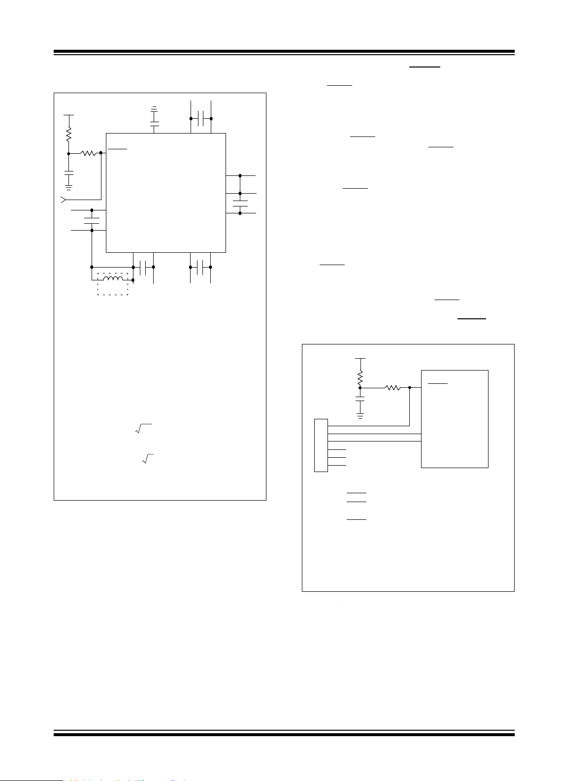
2.0 GUIDELINES FOR GETTING STARTED WITH 32-BIT MCUs
Note: This data sheet summarizes the features
of the PIC32MX1XX/2XX 28/36/44-pin
Family of devices. It is not intended to be
a comprehensive reference source. To
complement the information in this data
sheet, refer to the documents listed in the
Documentation > Reference Manual
section of the Microchip PIC32 web site
(www.microchip.com/pic32).
2.1 Basic Connection Requirements
Getting started with the PIC32MX1XX/2XX 28/36/44pin Family of 32-bit Microcontrollers (MCUs) requires
attention to a minimal set of device pin connections
before proceeding with development. The following is a
list of pin names, which must always be connected:
DD
•All V
•All AV
•V
•MCLR pin (see 2.4 “Master Clear (MCLR) Pin”)
• PGECx/PGEDx pins, used for In-Circuit Serial
• OSC1 and OSC2 pins, when external oscillator
The following pins may be required:
•V
and VSS pins (see 2.2 “Decoupling
Capacitors”)
DD
and AVSS pins, even if the ADC module
is not used (see 2.2 “Decoupling Capacitors”)
CAP
pin (see 2.3 “Capacitor on Internal
CAP
Voltage Regulator (V
Programming™ (ICSP™) and debugging purposes (see 2.5 “ICSP Pins”)
source is used (see 2.7 “External Oscillator
Pins”)
REF
+/V
REF
- pins – used when external voltage
reference for the ADC module is implemented
Note: The AV
nected, regardless of ADC use and the
ADC voltage reference source.
DD
)”)
and AVSS pins must be con-
2.2 Decoupling Capacitors
The use of decoupling capacitors on power supply
pins, such as V
See Figure 2-1.
Consider the following criteria when using decoupling
capacitors:
• Value and type of capacitor: A value of 0.1 µF
(100 nF), 10-20V is recommended. The capacitor
should be a low Equivalent Series Resistance
(low-ESR) capacitor and have resonance frequency in the range of 20 MHz and higher. It is
further recommended that ceramic capacitors be
used.
• Placement on the printed circuit board: The
decoupling capacitors should be placed as close
to the pins as possible. It is recommended that
the capacitors be placed on the same side of the
board as the device. If space is constricted, the
capacitor can be placed on another layer on the
PCB using a via; however, ensure that the trace
length from the pin to the capacitor is within onequarter inch (6 mm) in length.
• Handling high frequency noise: If the board is
experiencing high frequency noise, upward of
tens of MHz, add a second ceramic-type capacitor
in parallel to the above described decoupling
capacitor. The value of the second capacitor can
be in the range of 0.01 µF to 0.001 µF. Place this
second capacitor next to the primary decoupling
capacitor. In high-speed circuit designs, consider
implementing a decade pair of capacitances as
close to the power and ground pins as possible.
For example, 0.1 µF in parallel with 0.001 µF.
• Maximizing performance: On the board layout
from the power supply circuit, run the power and
return traces to the decoupling capacitors first,
and then to the device pins. This ensures that the
decoupling capacitors are first in the power chain.
Equally important is to keep the trace length
between the capacitor and the power pins to a
minimum thereby reducing PCB track inductance.
DD
, VSS, AVDD and AVSS is required.
2011-2019 Microchip Technology Inc. DS60001168L-page 27
PIC32MX1XX/2XX 28/36/44-PIN FAMILY
PIC32
V
DD
V
SS
V
DD
V
SS
V
SS
V
DD
AVDDAV
SS
VDDV
SS
0.1 µF
Ceramic
0.1 µF
Ceramic
0.1 µF
Ceramic
0.1 µF
Ceramic
C
10K
V
DD
MCLR
0.1 µF
Ceramic
L1
(2)
R1
Note 1: If the USB module is not used, this pin must be
connected to V
DD
.
2: As an option, instead of a hard-wired connection, an
inductor (L1) can be substituted between V
DD
and
AV
DD
to improve ADC noise rejection. The inductor
impedance should be less than 3 and the inductor
capacity greater than 10 mA.
Where:
f
F
CNV
2
------------ --
=
f
1
2 LC
------------ -----------
=
L
1
2fC
------------ ----------
2
=
(i.e., ADC conversion rate/2)
Connect
(2)
V
USB3V
3
(1)
V
CAP
Tantalum or
ceramic 10 µF
ESR 3
(3)
1: Aluminum or electrolytic capacitors should not be
used. ESR 3 from -40ºC to 125ºC @ SYSCLK
frequency (i.e., MIPS).
1K
0.1 µF
Note 1: 470R1 1 will limit any current flowing into
MCLR
from the external capacitor C, in the event of
MCLR
pin breakdown, due to Electrostatic Discharge
(ESD) or Electrical Overstress (EOS). Ensure that the
MCLR
pin VIH and VIL specifications are met without
interfering with the Debug/Programmer tools.
2: The capacitor can be sized to prevent unintentional
Resets from brief glitches or to extend the device
Reset period during POR.
3: No pull-ups or bypass capacitors are allowed on
active debug/program PGECx/PGEDx pins.
R1
(1)
10k
V
DD
MCLR
PIC32
1 k
0.1 µF
(2)
PGECx
(3)
PGEDx
(3)
ICSP™
1
5
4
2
3
6
V
DD
V
SS
NC
R
C
FIGURE 2-1: RECOMMENDED
MINIMUM CONNECTION
2.4 Master Clear (MCLR) Pin
The MCLR pin provides two specific device
functions:
• Device Reset
• Device programming and debugging
Pulling The MCLR
Figure 2-2 illustrates a typical MCLR circuit. During
device programming and debugging, the resistance
and capacitance that can be added to the pin must
be considered. Device programmers and debuggers
drive the MCLR
levels (V
IH
and VIL) and fast signal transitions must
not be adversely affected. Therefore, specific values
of R and C will need to be adjusted based on the
application and PCB requirements.
For example, as illustrated in Figure 2-2, it is
recommended that the capacitor C, be isolated from
the MCLR
pin during programming and debugging
operations.
Place the components illustrated in Figure 2-2 within
one-quarter inch (6 mm) from the MCLR
FIGURE 2-2: EXAMPLE OF MCLR PIN
pin low generates a device Reset.
pin. Consequently, specific voltage
pin.
CONNECTIONS
2.2.1 BULK CAPACITORS
The use of a bulk capacitor is recommended to improve
power supply stability. Typical values range from 4.7 µF
to 47 µF. This capacitor should be located as close to
the device as possible.
2.3 Capacitor on Internal Voltage
2.3.1 INTERNAL REGULATOR MODE
A low-ESR (3 ohm) capacitor is required on the V
pin, which is used to stabilize the internal voltage
regulator output. The V
to VDD, and must have a C
6V rating, connected to ground. The type can be
ceramic or tantalum. Refer to 30.0 “Electrical
Characteristics” for additional information on C
specifications.
DS60001168L-page 28 2011-2019 Microchip Technology Inc.
Regulator (V
CAP
)
CAP
pin must not be connected
EFC
capacitor, with at least a
CAP
EFC
2.5 ICSP Pins
The PGECx and PGEDx pins are used for ICSP and
debugging purposes. It is recommended to keep the
trace length between the ICSP connector and the ICSP
pins on the device as short as possible. If the ICSP connector is expected to experience an ESD event, a
series resistor is recommended, with the value in the
range of a few tens of Ohms, not to exceed 100 Ohms.

PIC32MX1XX/2XX 28/36/44-PIN FAMILY
Main Oscillator
Guard Ring
Guard Trace
Secondary
Oscillator
Pull-up resistors, series diodes and capacitors on the
PGECx and PGEDx pins are not recommended as they
will interfere with the programmer/debugger communications to the device. If such discrete components are
an application requirement, they should be removed
from the circuit during programming and debugging.
Alternatively, refer to the AC/DC characteristics and
timing requirements information in the respective
device Flash programming specification for information
on capacitive loading limits and pin input voltage high
IH
) and input low (VIL) requirements.
(V
Ensure that the “Communication Channel Select” (i.e.,
PGECx/PGEDx pins) programmed into the device
matches the physical connections for the ICSP to
MPLAB
®
ICD 3 or MPLAB REAL ICE™.
For more information on ICD 3 and REAL ICE
connection requirements, refer to the following
documents that are available on the Microchip web
site:
®
• “Using MPLAB
ICD 3” (poster) (DS50001765)
• “MPLAB® ICD 3 Design Advisory” (DS50001764)
• “MPLAB® REAL ICE™ In-Circuit Debugger
User’s Guide” (DS50001616)
®
• “Using MPLAB
REAL ICE™ Emulator” (poster)
(DS50001749)
The oscillator circuit should be placed on the same side
of the board as the device. Also, place the oscillator circuit close to the respective oscillator pins, not exceeding one-half inch (12 mm) distance between them. The
load capacitors should be placed next to the oscillator
itself, on the same side of the board. Use a grounded
copper pour around the oscillator circuit to isolate them
from surrounding circuits. The grounded copper pour
should be routed directly to the MCU ground. Do not
run any signal traces or power traces inside the ground
pour. Also, if using a two-sided board, avoid any traces
on the other side of the board where the crystal is
placed. A suggested layout is illustrated in Figure 2-3.
FIGURE 2-3: SUGGESTED OSCILLATOR
CIRCUIT PLACEMENT
2.6 JTAG
The TMS, TDO, TDI and TCK pins are used for testing
and debugging according to the Joint Test Action
Group (JTAG) standard. It is recommended to keep the
trace length between the JTAG connector and the
JTAG pins on the device as short as possible. If the
JTAG connector is expected to experience an ESD
event, a series resistor is recommended with the value
in the range of a few tens of Ohms, not to exceed 100
Ohms.
Pull-up resistors, series diodes and capacitors on the
TMS, TDO, TDI and TCK pins are not recommended
as they will interfere with the programmer/debugger
communications to the device. If such discrete components are an application requirement, they should be
removed from the circuit during programming and
debugging. Alternatively, refer to the AC/DC characteristics and timing requirements information in the
respective device Flash programming specification for
information on capacitive loading limits and pin input
IH
voltage high (V
) and input low (VIL) requirements.
2.7 External Oscillator Pins
Many MCUs have options for at least two oscillators: a
high-frequency primary oscillator and a low-frequency
secondary oscillator (refer to Section 8.0 “Oscillator
Configuration” for details).
2.8 Unused I/Os
Unused I/O pins should not be allowed to float as
inputs. They can be configured as outputs and driven
to a logic-low state.
Alternatively, inputs can be reserved by connecting the
SS
pin to V
the pin as an input.
through a 1k to 10k resistor and configuring
2011-2019 Microchip Technology Inc. DS60001168L-page 29

PIC32MX1XX/2XX 28/36/44-PIN FAMILY
Crystal manufacturer recommended: C1 = C2 = 15 pF
Therefore:
C
LOAD
= {( [CIN + C1] * [C
OUT
+ C2] ) / [CIN + C1 + C2 + C
OUT
]}
+ estimated oscillator PCB stray capacitance
= {( [5 + 15][5 + 15] ) / [5 + 15 + 15 + 5] } + 2.5 pF
= {( [20][20]) / [40] } + 2.5
= 10 + 2.5 = 12.5 pF
Rounded to the nearest standard value or 12 pF in this example for
Primary Oscillator crystals “C1” and “C2”.
OSC2 OSC1
1M
Typ ical XT
(4-10 MHz)
Circuit A
C1
C2
OSC2 OSC1
Typ ical HS
(10-25 MHz)
Circuit B
C1
C2
Rs
OSC2
OSC1
1M
Typic al XT/ HS
(4-25 MHz)
Circuit C
C1
C2
1M
Rs
OSC2
OSC1
Not Recommended
Circuit D
Not Recommended
1M
Rs
OSC2 OSC1
Circuit E
2.8.1 CRYSTAL OSCILLATOR DESIGN
CONSIDERATION
The following example assumptions are used to
calculate the Primary Oscillator loading capacitor
values:
IN
= PIC32_OSC2_Pin Capacitance = ~4-5 pF
•C
OUT
•C
= PIC32_OSC1_Pin Capacitance = ~4-5 pF
• C1 and C2 = XTAL manufacturing recommended
loading capacitance
• Estimated PCB stray capacitance, (i.e.,12 mm
length) = 2.5 pF
EXAMPLE 2-1: CRYSTAL LOAD CAPACITOR
CALCULATION
The following tips are used to increase oscillator gain,
(i.e., to increase peak-to-peak oscillator signal):
• Select a crystal with a lower “minimum” power drive
rating
• Select an crystal oscillator with a lower XTAL
manufacturing “ESR” rating.
• Add a parallel resistor across the crystal. The smaller
the resistor value the greater the gain. It is recommended to stay in the range of 600k to 1M
• C1 and C2 values also affect the gain of the oscillator.
The lower the values, the higher the gain.
• C2/C1 ratio also affects gain. To increase the gain,
make C1 slightly smaller than C2, which will also help
start-up performance.
Note: Do not add excessive gain such that the
oscillator signal is clipped, flat on top of
the sine wave. If so, you need to reduce
the gain or add a series resistor, RS, as
shown in circuit “C” in Figure 2-4. Failure
to do so will stress and age the crystal,
which can result in an early failure. Adjust
the gain to trim the max peak-to-peak to
~V
DD
-0.6V. When measuring the oscilla-
tor signal you must use a FET scope
probe or a probe with 1.5 pF or the
scope probe itself will unduly change the
gain and peak-to-peak levels.
2.8.1.1 Additional Microchip References
• AN588 “PICmicro® Microcontroller Oscill ato r
• AN826 “Crystal Oscillator Basics and Crystal
• AN849 “Basic PICmicro® Oscillator Design”
DS60001168L-page 30 2011-2019 Microchip Technology Inc.
Design Guide”
Selection for rfPIC™ and PICmicro
®
FIGURE 2-4: PRIMARY CRYSTAL
OSCILLATOR CIRCUIT
RECOMMENDATIONS
Devices”
PIC32MX1XX/2XX 28/36/44-PIN FAMILY
CTMU
Current Source
ADC
Microchip
mTouch™
Library
User
Application
Microchip
Graphics
Library
Read the Touch Sensors
Process Samples
Display Data
Parallel
Master
Port
LCD Controller
Frame
Buffer
Display
Controller
PMPD<7:0>
LCD
Panel
PIC32MX120F032D
To A N6 To A N7 To A N8 To A N1 1
C1
R3
C2
R2
R3
R1
C5
C5
C5
C1
R1
R1
R1
C3
R2
C3
R2
C1
R2
C2
R3
C2
R3
C3
AN0
AN1
AN11
To A N0
To A N1
To A N5
AN9
PMPWR
To AN 9
R1
C4
R2
C4
R3
C4
Audio
Codec
Display
PMP
I
2
S
SPI
USB
USB
PMPD<7:0>
3
3
Stereo Headphones
Speaker
PIC32MX220F032D
Host
PMPWR
MMC SD
3
SDI
2.9 Typical Application Connection Examples
Examples of typical application connections are shown
in Figure 2-5 and Figure 2-6.
FIGURE 2-5: CAPACITIVE TOUCH SENSING WITH GRAPHICS APPLICATION
FIGURE 2-6: AUDIO PLAYBACK APPLICATION
2011-2019 Microchip Technology Inc. DS60001168L-page 31

PIC32MX1XX/2XX 28/36/44-PIN FAMILY
2.10 Considerations When Interfacing To Remotely Powered Circuits
2.10.1 NON-5V TOLERANT INPUT PINS
A quick review of the maximum rating section in the
Section 30.0 “Electrical Characteristics” will
indicate that the voltage on any non-5V tolerant pin
should not exceed AVDD/VDD+0.3V. Figure 2-7
illustrates a remote circuit using an independent power
source that is powered while connected to a PIC32
non-5V tolerant circuit which is not powered.
FIGURE 2-7: REMOTE CIRCUIT WITH AN INDEPENDENT POWER SOURCE
DS60001168L-page 32 2011-2019 Microchip Technology Inc.
PIC32MX1XX/2XX 28/36/44-PIN FAMILY
Without proper signal isolation on non-5V tolerant
pins, the remote signal can power the PIC32 through
the high side ESD protection diodes. This violates the
maximum rating specification and can cause improper
initialization of internal PIC32 logic circuits. In this
case, it is recommended that users can implement a
digital or analog signal isolation, as shown in Figure 2-
8.
FIGURE 2-8: DIGITAL AND ANALOG SIGNAL ISOLATION
Digital signal isolators along with optional level
translation examples are provided in Ta bl e 2 - 1.
TABLE 2-1: EXAMPLES OF DIGITAL ISOLATORS WITH OPTIONAL LEVEL TRANSLATION
Inductive Coupling
ADuM7241 / 40 ARZ (1Mbps) X - - -
ADuM7241 / 40 CRZ (25 Mbps) X - - -
ISO721 - X - -
LTV-829S (2 Chan) - - X -
LTV-849S (4 Chan) ----
FSA266 / NC7WB66 - - - X
Capacitive Coupling
Optional Coupling
Analog/Digital Switch
2011-2019 Microchip Technology Inc. DS60001168L-page 33

PIC32MX1XX/2XX 28/36/44-PIN FAMILY
2.10.2 5V-TOLERANT INPUT PINS
The internal high-side diode on 5V-tolerant pins, rather
than being connected to VDD, are bussed to an
internal floating node, as shown in Figure 2-9.
Voltages on these pins, if VDD < 2.3V, should not
exceed roughly 3.2V relative to PIC32 VSS. At 3.6V or
above, it will violate the absolute maximum
specification and impact the device reliability.
If a remotely powered digital only signal can be
guaranteed to always be ≤ 3.2V relative to PIC32 VSS,
then a 5V-tolerant pin can be used without a digital
isolator. This can be assumed when the following is
applicable:
• No ground loop issue
• The logic ground of the two circuits is not at the
same absolute level
• No remote logic low inputs are less than VSS -
0.3V
FIGURE 2-9: 5V-TOLERANT INPUT PINS BUSSED TO AN INTERNAL FLOATING NODE
DS60001168L-page 34 2011-2019 Microchip Technology Inc.

PIC32MX1XX/2XX 28/36/44-PIN FAMILY
V
SS
V
DD
V
SS
V
USB3V3
V
SS
V
DD
V
SS
V
DD
V
DD
V
SS
V
SS
V
DD
V
SS
V
DD
VSSV
DD
AVDDAV
SS
Ferrite
Chips
0.01 μF
0.01 μF
V
DD
V
DD
0.1 μF
0.1 μF
0.1 μF
0.1 μF
0.1 μF
0.1 μF
0.1 μF
0.1 μF
Ferrite
Chips
Ferrite Chip SMD
DCR = 0.15ȍ (max)
600 ma ISAT
300ȍ @ 100 MHz
PN#: 1-1624117-3
0.1 μF
PIC32
2.11 EMI/EMC/EFT (IEC 61000-4-4 and IEC 61000-4-2) Suppression Considerations
The use of LDO regulators is preferred to reduce
overall system noise and provide a cleaner power
source. However, when utilizing switching
Buck/Boost regulators as the local power source for
PIC32 devices, as well as in electrically noisy environments or test conditions required for IEC 610004-4 and IEC 61000-4-2, users should evaluate the
use of T-Filters (i.e., L-C-L) on the power pins, as
shown in Figure 2-10. In addition to a more stable
power source, using this type of T-Filter can greatly
reduce susceptibility to EMI sources and events.
FIGURE 2-10: EMI/EMC/EFT
SUPPRESSION CIRCUIT
2011-2019 Microchip Technology Inc. DS60001168L-page 35

PIC32MX1XX/2XX 28/36/44-PIN FAMILY
NOTES:
DS60001168L-page 36 2011-2019 Microchip Technology Inc.

PIC32MX1XX/2XX 28/36/44-PIN FAMILY
CPU
MDU
Execution Core
(RF/ALU/Shift)
FMT
TAP
EJTAG
Bus Interface
Power
Management
System
Co-processor
Off-chip Debug Interface
Bus Matrix
Dual Bus Interface
3.0 CPU
Note: This data sheet summarizes the features
of the PIC32MX1XX/2XX 28/36/44-pin
Family of devices. It is not intended to be
a comprehensive reference source. To
complement the information in this data
sheet, refer to Section 2. “CPU”
(DS60001113), which is available from the
Documentation > Reference Manual
section of the Microchip PIC32 web site
(www.microchip.com/pic32). Resources
for the MIPS32
are available at: www.imgtec.com.
The MIPS32® M4K® Processor Core is the heart of the
PIC32MX1XX/2XX family processor. The CPU fetches
instructions, decodes each instruction, fetches source
operands, executes each instruction and writes the
results of instruction execution to the destinations.
3.1 Features
• 5-stage pipeline
• 32-bit address and data paths
• MIPS32 Enhanced Architecture (Release 2)
- Multiply-accumulate and multiply-subtract
instructions
- Targeted multiply instruction
- Zero/One detect instructions
- WAIT instruction
- Conditional move instructions (MOVN, MOVZ)
- Vectored interrupts
- Programmable exception vector base
- Atomic interrupt enable/disable
- Bit field manipulation instructions
®
M4K® Processor Core
• MIPS16e
®
code compression
- 16-bit encoding of 32-bit instructions to
improve code density
- Special PC-relative instructions for efficient
loading of addresses and constants
- SAVE and RESTORE macro instructions for
setting up and tearing down stack frames
within subroutines
- Improved support for handling 8 and 16-bit
data types
• Simple Fixed Mapping Translation (FMT)
mechanism
• Simple dual bus interface
- Independent 32-bit address and data buses
- Transactions can be aborted to improve
interrupt latency
• Autonomous multiply/divide unit
- Maximum issue rate of one 32x16 multiply
per clock
- Maximum issue rate of one 32x32 multiply
every other clock
- Early-in iterative divide. Minimum 11 and
maximum 33 clock latency (dividend (rs) sign
extension-dependent)
• Power control
- Minimum frequency: 0 MHz
- Low-Power mode (triggered by WAIT
instruction)
- Extensive use of local gated clocks
• EJTAG debug and instruction trace
- Support for single stepping
- Virtual instruction and data address/value
-Breakpoints
FIGURE 3-1: MIPS32® M4K® PROCESSOR CORE BLOCK DIAGRAM
2011-2019 Microchip Technology Inc. DS60001168L-page 37

PIC32MX1XX/2XX 28/36/44-PIN FAMILY
3.2 Architecture Overview
The MIPS32 M4K processor core contains several
logic blocks working together in parallel, providing an
efficient high-performance computing engine. The
following blocks are included with the core:
• Execution Unit
• Multiply/Divide Unit (MDU)
• System Control Coprocessor (CP0)
• Fixed Mapping Translation (FMT)
• Dual Internal Bus interfaces
• Power Management
• MIPS16e
• Enhanced JTAG (EJTAG) Controller
3.2.1 EXECUTION UNIT
The MIPS32 M4K processor core execution unit implements a load/store architecture with single-cycle ALU
operations (logical, shift, add, subtract) and an autonomous multiply/divide unit. The core contains thirty-two
32-bit General Purpose Registers (GPRs) used for
integer operations and address calculation. The register file consists of two read ports and one write port and
is fully bypassed to minimize operation latency in the
pipeline.
The execution unit includes:
• 32-bit adder used for calculating the data address
• Address unit for calculating the next instruction
address
• Logic for branch determination and branch target
address calculation
• Load aligner
• Bypass multiplexers used to avoid stalls when
executing instruction streams where data
producing instructions are followed closely by
consumers of their results
• Leading Zero/One detect unit for implementing
the CLZ and CLO instructions
• Arithmetic Logic Unit (ALU) for performing bitwise
logical operations
• Shifter and store aligner
®
Support
3.2.2 MULTIPLY/DIVIDE UNIT (MDU)
The MIPS32 M4K processor core includes a Multiply/Divide Unit (MDU) that contains a separate pipeline
for multiply and divide operations. This pipeline operates in parallel with the Integer Unit (IU) pipeline and
does not stall when the IU pipeline stalls. This allows
MDU operations to be partially masked by system stalls
and/or other integer unit instructions.
The high-performance MDU consists of a 32x16 booth
recoded multiplier, result/accumulation registers (HI
and LO), a divide state machine, and the necessary
multiplexers and control logic. The first number shown
(‘32’ of 32x16) represents the rs operand. The second
number (‘16’ of 32x16) represents the rt operand. The
PIC32 core only checks the value of the latter (rt) oper-
and to determine how many times the operation must
pass through the multiplier. The 16x16 and 32x16
operations pass through the multiplier once. A 32x32
operation passes through the multiplier twice.
The MDU supports execution of one 16x16 or 32x16
multiply operation every clock cycle; 32x32 multiply
operations can be issued every other clock cycle.
Appropriate interlocks are implemented to stall the
issuance of back-to-back 32x32 multiply operations.
The multiply operand size is automatically determined
by logic built into the MDU.
Divide operations are implemented with a simple 1 bit
per clock iterative algorithm. An early-in detection
checks the sign extension of the dividend (rs) operand.
If rs is 8 bits wide, 23 iterations are skipped. For a 16-bit
wide rs, 15 iterations are skipped and for a 24-bit wide
rs, 7 iterations are skipped. Any attempt to issue a subsequent MDU instruction while a divide is still active
causes an IU pipeline stall until the divide operation is
completed.
Table 3-1 lists the repeat rate (peak issue rate of cycles
until the operation can be reissued) and latency (number of cycles until a result is available) for the PIC32
core multiply and divide instructions. The approximate
latency and repeat rates are listed in terms of pipeline
clocks.
TABLE 3-1: MIPS32® M4K® PROCESSOR CORE HIGH-PERFORMANCE INTEGER
MULTIPLY/DIVIDE UNIT LATENCIES AND REPEAT RATES
Opcode Operand Size (mul rt) (div rs) Latency Repeat Rate
MULT/MULTU, MADD/MADDU,
MSUB/MSUBU
MUL 16 bits 2 1
DIV/DIVU 8 bits 12 11
DS60001168L-page 38 2011-2019 Microchip Technology Inc.
16 bits 1 1
32 bits 2 2
32 bits 3 2
16 bits 19 18
24 bits 26 25
32 bits 33 32

PIC32MX1XX/2XX 28/36/44-PIN FAMILY
The MIPS architecture defines that the result of a
multiply or divide operation be placed in the HI and LO
registers. Using the Move-From-HI (MFHI) and MoveFrom-LO (MFLO) instructions, these values can be
transferred to the General Purpose Register file.
In addition to the HI/LO targeted operations, the
MIPS32
®
architecture also defines a multiply instruc-
tion, MUL, which places the least significant results in
the primary register file instead of the HI/LO register
pair. By avoiding the explicit MFLO instruction
required when using the LO register, and by supporting multiple destination registers, the throughput of
multiply-intensive operations is increased.
Two other instructions, Multiply-Add (MADD) and
Multiply-Subtract (MSUB), are used to perform the
multiply-accumulate and multiply-subtract operations.
adds the product to the current contents of the HI and
LO registers. Similarly, the MSUB instruction multiplies
two operands and then subtracts the product from the
HI and LO registers. The MADD and MSUB operations
are commonly used in DSP algorithms.
3.2.3 SYSTEM CONTROL
COPROCESSOR (CP0)
In the MIPS architecture, CP0 is responsible for the
virtual-to-physical address translation, the exception
control system, the processor’s diagnostics capability,
the operating modes (Kernel, User and Debug) and
whether interrupts are enabled or disabled. Configuration information, such as presence of options like
MIPS16e, is also available by accessing the CP0
registers, listed in Ta bl e 3 -2 .
The MADD instruction multiplies two numbers and then
TABLE 3-2: COPROCESSOR 0 REGISTERS
Register
Number
0-6 Reserved Reserved in the PIC32MX1XX/2XX family core.
7 HWREna Enables access via the RDHWR instruction to selected hardware registers.
8 BadVAddr
9 Count
10 Reserved Reserved in the PIC32MX1XX/2XX family core.
11 Compare
12 Status
12 IntCtl
12 SRSCtl
12 SRSMap
13 Cause
14 EPC
15 PRId Processor identification and revision.
15 EBASE Exception vector base register.
16 Config Configuration register.
16 Config1 Configuration Register 1.
16 Config2 Configuration Register 2.
16 Config3 Configuration Register 3.
17-22 Reserved Reserved in the PIC32MX1XX/2XX family core.
23 Debug
24 DEPC
25-29 Reserved Reserved in the PIC32MX1XX/2XX family core.
30 ErrorEPC
31 DESAVE
Note 1: Registers used in exception processing.
2: Registers used during debug.
Register
Name
(1)
(1)
(1)
(1)
(1)
(1)
(1)
(1)
(1)
(2)
(2)
(1)
(2)
Function
Reports the address for the most recent address-related exception.
Processor cycle count.
Timer interrupt control.
Processor status and control.
Interrupt system status and control.
Shadow register set status and control.
Provides mapping from vectored interrupt to a shadow set.
Cause of last general exception.
Program counter at last exception.
Debug control and exception status.
Program counter at last debug exception.
Program counter at last error.
Debug handler scratchpad register.
2011-2019 Microchip Technology Inc. DS60001168L-page 39

PIC32MX1XX/2XX 28/36/44-PIN FAMILY
Coprocessor 0 also contains the logic for identifying
and managing exceptions. Exceptions can be caused
by a variety of sources, including alignment errors in
data, external events or program errors. Ta bl e 3 - 3 lists
the exception types in order of priority.
TABLE 3-3: MIPS32® M4K® PROCESSOR CORE EXCEPTION TYPES
Exception Description
Reset Assertion MCLR
DSS EJTAG debug single step.
DINT EJTAG debug interrupt. Caused by the assertion of the external EJ_DINT input or by setting the
EjtagBrk bit in the ECR register.
NMI Assertion of NMI signal.
Interrupt Assertion of unmasked hardware or software interrupt signal.
DIB EJTAG debug hardware instruction break matched.
AdEL Fetch address alignment error.
Fetch reference to protected address.
IBE Instruction fetch bus error.
DBp EJTAG breakpoint (execution of SDBBP instruction).
Sys Execution of SYSCALL instruction.
Bp Execution of BREAK instruction.
RI Execution of a reserved instruction.
CpU Execution of a coprocessor instruction for a coprocessor that is not enabled.
CEU Execution of a CorExtend instruction when CorExtend is not enabled.
Ov Execution of an arithmetic instruction that overflowed.
Tr Execution of a trap (when trap condition is true).
DDBL/DDBS EJTAG Data Address Break (address only) or EJTAG data value break on store (address + value).
AdEL Load address alignment error.
Load reference to protected address.
AdES Store address alignment error.
Store to protected address.
DBE Load or store bus error.
DDBL EJTAG data hardware breakpoint matched in load data compare.
or a Power-on Reset (POR).
3.3 Power Management
The MIPS M4K processor core offers many power management features, including low-power design, active
power management and power-down modes of operation. The core is a static design that supports slowing or
Halting the clocks, which reduces system power consumption during Idle periods.
3.3.1 INSTRUCTION-CONTROLLED
POWER MANAGEMENT
The mechanism for invoking Power-Down mode is
through execution of the WAIT instruction. For more
information on power management, see Section 26.0
“Power-Saving Features”.
DS60001168L-page 40 2011-2019 Microchip Technology Inc.
3.4 EJTAG Debug Support
The MIPS M4K processor core provides an Enhanced
JTAG (EJTAG) interface for use in the software debug
of application and kernel code. In addition to standard
User mode and Kernel modes of operation, the M4K
core provides a Debug mode that is entered after a
debug exception (derived from a hardware breakpoint,
single-step exception, etc.) is taken and continues until
a Debug Exception Return (DERET) instruction is
executed. During this time, the processor executes the
debug exception handler routine.
The EJTAG interface operates through the Test Access
Port (TAP), a serial communication port used for transferring test data in and out of the core. In addition to the
standard JTAG instructions, special instructions
defined in the EJTAG specification define which
registers are selected and how they are used.

PIC32MX1XX/2XX 28/36/44-PIN FAMILY
4.0 MEMORY ORGANIZATION
Note: This data sheet summarizes the features
of the PIC32MX1XX/2XX 28/36/44-pin
Family of devices. It is not intended to be
a comprehensive reference source.For
detailed information, refer to Section 3.
“Memory Organization” (DS60001115),
which is available from the
Documentation > Reference Manual
section of the Microchip PIC32 web site
(www.microchip.com/pic32).
PIC32MX1XX/2XX 28/36/44-pin Family microcontrollers provide 4 GB unified virtual memory address
space. All memory regions, including program, data
memory, Special Function Registers (SFRs), and Configuration registers, reside in this address space at their
respective unique addresses. The program and data
memories can be optionally partitioned into user and
kernel memories. In addition, the data memory can be
made executable, allowing PIC32MX1XX/2XX
28/36/44-pin Family devices to execute from data
memory.
Key features include:
• 32-bit native data width
• Separate User (KUSEG) and Kernel
(KSEG0/KSEG1) mode address space
• Flexible program Flash memory partitioning
• Flexible data RAM partitioning for data and
program space
• Separate boot Flash memory for protected code
• Robust bus exception handling to intercept
runaway code
• Simple memory mapping with Fixed Mapping
Translation (FMT) unit
• Cacheable (KSEG0) and non-cacheable (KSEG1)
address regions
4.1 PIC32MX1XX/2XX 28/36/44-pin Family Memory Layout
PIC32MX1XX/2XX 28/36/44-pin Family microcontrollers implement two address schemes: virtual and physical. All hardware resources, such as program memory,
data memory and peripherals, are located at their
respective physical addresses. Virtual addresses are
exclusively used by the CPU to fetch and execute
instructions as well as access peripherals. Physical
addresses are used by bus master peripherals, such as
DMA and the Flash controller, that access memory
independently of the CPU.
The memory maps for the PIC32MX1XX/2XX
28/36/44-pin Family devices are illustrated in
Figure 4-1 through Figure 4-6.
Table 4-1 provides SFR memory map details.
2011-2019 Microchip Technology Inc. DS60001168L-page 41

PIC32MX1XX/2XX 28/36/44-PIN FAMILY
Virtual
Memory Map
(1)
Physical
Memory Map
(1)
0xFFFFFFFF
Reserved
Reserved
0xFFFFFFFF
0xBFC00C00
0xBFC00BFF
Device
Configuration
Registers
0xBFC00BF0
0xBFC00BEF
Boot Flash
0xBFC00000
Reserved
0xBF900000
0xBF8FFFFF
SFRs
0xBF800000
Reserved
0xBD004000
0xBD003FFF
Program Flash
(2)
0xBD000000
Reserved
0xA0001000
0xA0000FFF
RAM
(2)
0xA0000000 0x1FC00C00
Reserved
Device
Configuration
Registers
0x1FC00BFF
0x9FC00C00
0x9FC00BFF Device
Configuration
Registers
0x1FC00BF0
Boot Flash
0x1FC00BEF
0x9FC00BF0
0x9FC00BEF
Boot Flash
0x1FC00000
Reserved
0x9FC00000 0x1F900000
Reserved SFRs
0x1F8FFFFF
0x9D004000 0x1F800000
0x9D003FFF
Program Flash
(2)
Reserved
0x9D000000 0x1D004000
Reserved
Program Flash
(2)
0x1D003FFF
0x80001000
0x80000FFF
RAM
(2)
0x1D000000
Reserved
0x80000000 0x00001000
Reserved RAM
(2)
0x00000FFF
0x00000000 0x00000000
Note 1: Memory areas are not shown to scale.
2: The size of this memory region is programmable (see Section 3. “Memory Organization”
(DS60001115) in the “PIC32 Family Reference Manual”) and can be changed by initialization code provided by end-user development tools (refer to the specific development tool
documentation for information).
KSEG1KSEG0
FIGURE 4-1: MEMORY MAP ON RESET FOR PIC32MX110/210 DEVICES (4 KB RAM, 16 KB FLASH)
DS60001168L-page 42 2011-2019 Microchip Technology Inc.
PIC32MX1XX/2XX 28/36/44-PIN FAMILY
Virtual
Memory Map
(1)
Physical
Memory Map
(1)
0xFFFFFFFF
Reserved
Reserved
0xFFFFFFFF
0xBFC00C00
0xBFC00BFF
Device
Configuration
Registers
0xBFC00BF0
0xBFC00BEF
Boot Flash
0xBFC00000
Reserved
0xBF900000
0xBF8FFFFF
SFRs
0xBF800000
Reserved
0xBD008000
0xBD007FFF
Program Flash
(2)
0xBD000000
Reserved
0xA0002000
0xA0001FFF
RAM
(2)
0xA0000000 0x1FC00C00
Reserved
Device
Configuration
Registers
0x1FC00BFF
0x9FC00C00
0x9FC00BFF Device
Configuration
Registers
0x1FC00BF0
Boot Flash
0x1FC00BEF
0x9FC00BF0
0x9FC00BEF
Boot Flash
0x1FC00000
Reserved
0x9FC00000 0x1F900000
Reserved SFRs
0x1F8FFFFF
0x9D008000 0x1F800000
0x9D007FFF
Program Flash
(2)
Reserved
0x9D000000 0x1D008000
Reserved
Program Flash
(2)
0x1D007FFF
0x80002000
0x80001FFF
RAM
(2)
0x1D000000
Reserved
0x80000000 0x00002000
Reserved RAM
(2)
0x00001FFF
0x00000000 0x00000000
Note 1: Memory areas are not shown to scale.
2: The size of this memory region is programmable (see Section 3. “Memory Organization”
(DS60001115) in the “PIC32 Family Reference Manual”) and can be changed by initialization code provided by end-user development tools (refer to the specific development tool
documentation for information).
KSEG1KSEG0
FIGURE 4-2: MEMORY MAP ON RESET FOR PIC32MX120/220 DEVICES (8 KB RAM, 32 KB FLASH)
2011-2019 Microchip Technology Inc. DS60001168L-page 43

PIC32MX1XX/2XX 28/36/44-PIN FAMILY
Virtual
Memory Map
(1)
Physical
Memory Map
(1)
0xFFFFFFFF
Reserved
Reserved
0xFFFFFFFF
0xBFC00C00
0xBFC00BFF
Device
Configuration
Registers
0xBFC00BF0
0xBFC00BEF
Boot Flash
0xBFC00000
Reserved
0xBF900000
0xBF8FFFFF
SFRs
0xBF800000
Reserved
0xBD010000
0xBD00FFFF
Program Flash
(2)
0xBD000000
Reserved
0xA0004000
0xA0003FFF
RAM
(2)
0xA0000000 0x1FC00C00
Reserved
Device
Configuration
Registers
0x1FC00BFF
0x9FC00C00
0x9FC00BFF Device
Configuration
Registers
0x1FC00BF0
Boot Flash
0x1FC00BEF
0x9FC00BF0
0x9FC00BEF
Boot Flash
0x1FC00000
Reserved
0x9FC00000 0x1F900000
Reserved SFRs
0x1F8FFFFF
0x9D010000 0x1F800000
0x9D00FFFF
Program Flash
(2)
Reserved
0x9D000000 0x1D010000
Reserved
Program Flash
(2)
0x1D00FFFF
0x80004000
0x80003FFF
RAM
(2)
0x1D000000
Reserved
0x80000000 0x00004000
Reserved RAM
(2)
0x00003FFF
0x00000000 0x00000000
Note 1: Memory areas are not shown to scale.
2: The size of this memory region is programmable (see Section 3. “Memory Organization”
(DS60001115) in the “PIC32 Family Reference Manual”) and can be changed by initialization code provided by end-user development tools (refer to the specific development tool
documentation for information).
KSEG1KSEG0
FIGURE 4-3: MEMORY MAP ON RESET FOR PIC32MX130/230 DEVICES (16 KB RAM, 64 KB FLASH)
DS60001168L-page 44 2011-2019 Microchip Technology Inc.

PIC32MX1XX/2XX 28/36/44-PIN FAMILY
Virtual
Memory Map
(1)
Physical
Memory Map
(1)
0xFFFFFFFF
Reserved
Reserved
0xFFFFFFFF
0xBFC00C00
0xBFC00BFF
Device
Configuration
Registers
0xBFC00BF0
0xBFC00BEF
Boot Flash
0xBFC00000
Reserved
0xBF900000
0xBF8FFFFF
SFRs
0xBF800000
Reserved
0xBD020000
0xBD01FFFF
Program Flash
(2)
0xBD000000
Reserved
0xA0008000
0xA0007FFF
RAM
(2)
0xA0000000 0x1FC00C00
Reserved
Device
Configuration
Registers
0x1FC00BFF
0x9FC00C00
0x9FC00BFF Device
Configuration
Registers
0x1FC00BF0
Boot Flash
0x1FC00BEF
0x9FC00BF0
0x9FC00BEF
Boot Flash
0x1FC00000
Reserved
0x9FC00000 0x1F900000
Reserved SFRs
0x1F8FFFFF
0x9D020000 0x1F800000
0x9D01FFFF
Program Flash
(2)
Reserved
0x9D000000 0x1D020000
Reserved
Program Flash
(2)
0x1D01FFFF
0x80008000
0x80007FFF
RAM
(2)
0x1D000000
Reserved
0x80000000 0x00008000
Reserved RAM
(2)
0x00007FFF
0x00000000 0x00000000
Note 1: Memory areas are not shown to scale.
2: The size of this memory region is programmable (see Section 3. “Memory Organization”
(DS60001115) in the “PIC32 Family Reference Manual”) and can be changed by initialization code provided by end-user development tools (refer to the specific development tool
documentation for information).
KSEG1KSEG0
FIGURE 4-4: MEMORY MAP ON RESET FOR PIC32MX150/250 DEVICES (32 KB RAM, 128 KB FLASH)
2011-2019 Microchip Technology Inc. DS60001168L-page 45
PIC32MX1XX/2XX 28/36/44-PIN FAMILY
Virtual
Memory Map
(1)
Physical
Memory Map
(1)
0xFFFFFFFF
Reserved
Reserved
0xFFFFFFFF
0xBFC00C00
0xBFC00BFF
Device
Configuration
Registers
0xBFC00BF0
0xBFC00BEF
Boot Flash
0xBFC00000
Reserved
0xBF900000
0xBF8FFFFF
SFRs
0xBF800000
Reserved
0xBD040000
0xBD03FFFF
Program Flash
(2)
0xBD000000
Reserved
0xA0010000
0xA000FFFF
RAM
(2)
0xA0000000 0x1FC00C00
Reserved
Device
Configuration
Registers
0x1FC00BFF
0x9FC00C00
0x9FC00BFF Device
Configuration
Registers
0x1FC00BF0
Boot Flash
0x1FC00BEF
0x9FC00BF0
0x9FC00BEF
Boot Flash
0x1FC00000
Reserved
0x9FC00000 0x1F900000
Reserved SFRs
0x1F8FFFFF
0x9D040000 0x1F800000
0x9D03FFFF
Program Flash
(2)
Reserved
0x9D000000 0x1D040000
Reserved
Program Flash
(2)
0x1D03FFFF
0x80010000
0x8000FFFF
RAM
(2)
0x1D000000
Reserved
0x80000000 0x00010000
Reserved RAM
(2)
0x0000FFFF
0x00000000 0x00000000
Note 1: Memory areas are not shown to scale.
2: The size of this memory region is programmable (see Section 3. “Memory Organization”
(DS60001115) in the “PIC32 Family Reference Manual”) and can be changed by initialization code provided by end-user development tools (refer to the specific development tool
documentation for information).
KSEG1KSEG0
FIGURE 4-5: MEMORY MAP ON RESET FOR PIC32MX170/270 DEVICES (64 KB RAM, 256 KB FLASH)
DS60001168L-page 46 2011-2019 Microchip Technology Inc.

PIC32MX1XX/2XX 28/36/44-PIN FAMILY
Virtual
Memory Map
(1)
Physical
Memory Map
(1)
0xFFFFFFFF
Reserved
Reserved
0xFFFFFFFF
0xBFC00C00
0xBFC00BFF
Device
Configuration
Registers
0xBFC00BF0
0xBFC00BEF
Boot Flash
0xBFC00000
Reserved
0xBF900000
0xBF8FFFFF
SFRs
0xBF800000
Reserved
0xBD040000
0xBD03FFFF
Program Flash
(2)
0xBD000000
Reserved
0xA0004000
0xA0003FFF
RAM
(2)
0xA0000000 0x1FC00C00
Reserved
Device
Configuration
Registers
0x1FC00BFF
0x9FC00C00
0x9FC00BFF Device
Configuration
Registers
0x1FC00BF0
Boot Flash
0x1FC00BEF
0x9FC00BF0
0x9FC00BEF
Boot Flash
0x1FC00000
Reserved
0x9FC00000 0x1F900000
Reserved SFRs
0x1F8FFFFF
0x9D040000 0x1F800000
0x9D03FFFF
Program Flash
(2)
Reserved
0x9D000000 0x1D040000
Reserved
Program Flash
(2)
0x1D03FFFF
0x80004000
0x80003FFF
RAM
(2)
0x1D000000
Reserved
0x80000000 0x00004000
Reserved RAM
(2)
0x00003FFF
0x00000000 0x00000000
Note 1: Memory areas are not shown to scale.
2: The size of this memory region is programmable (see Section 3. “Memory Organization”
(DS60001115) in the “PIC32 Family Reference Manual”) and can be changed by initialization code provided by end-user development tools (refer to the specific development tool
documentation for information).
KSEG1KSEG0
FIGURE 4-6: MEMORY MAP ON RESET FOR PIC32MX130/230 DEVICES (16 KB RAM, 256 KB FLASH)
2011-2019 Microchip Technology Inc. DS60001168L-page 47

PIC32MX1XX/2XX 28/36/44-PIN FAMILY
TABLE 4-1: SFR MEMORY MAP
Virtual Address
Peripheral
Watchdog Timer
RTCC 0x0200
Timer1-5 0x0600
Input Capture 1-5 0x2000
Output Compare 1-5 0x3000
IC1 and IC2 0x5000
SPI1 and SPI2 0x5800
UART1 and UART2 0x6000
PMP 0x7000
ADC 0x9000
REF
CV
Comparator 0xA000
CTMU 0xA200
Oscillator 0xF000
Device and Revision ID 0xF220
Peripheral Module Disable 0xF240
Flash Controller 0xF400
Reset 0xF600
PPS 0xFA04
Interrupts
Bus Matrix 0x2000
DMA 0x3000
USB 0x5050
PORTA-PORTC 0x6000
Configuration
Base
0xBF80
0xBF88
0xBFC0
Offset
Start
0x0000
0x9800
0x1000
0x0BF0
DS60001168L-page 48 2011-2019 Microchip Technology Inc.
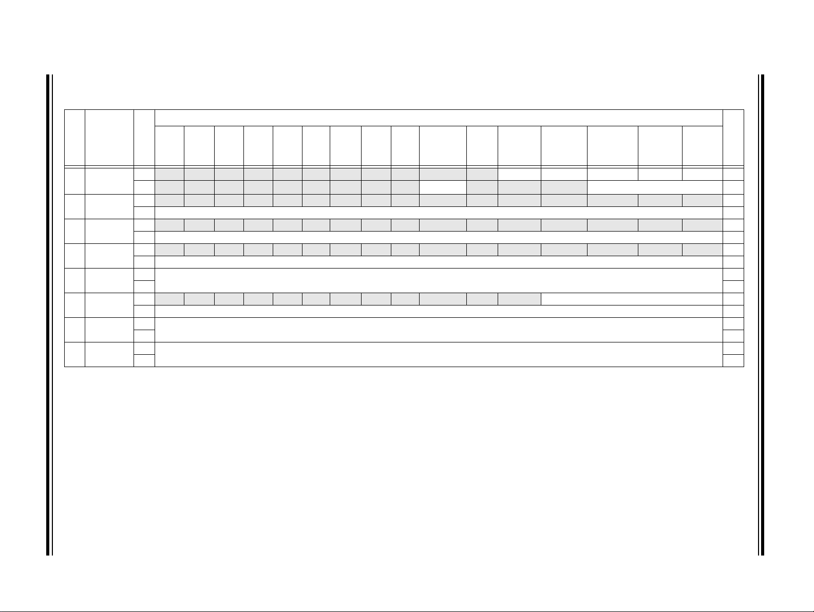
2011-2019 Microchip Technology Inc. DS60001168L-page 49
4.2 Bus Matrix Control Registers
TABLE 4-2: BUS MATRIX REGISTER MAP
Bits
Name
Register
(BF88_#)
Virtual Address
2000 BMXCON
2010 BMXDKPBA
2020 BMXDUDBA
2030 BMXDUPBA
2040 BMXDRMSZ
2050 BMXPUPBA
2060 BMXPFMSZ
2070 BMXBOOTSZ
Legend: x = unknown value on Reset; — = unimplemented, read as ‘0’. Reset values are shown in hexadecimal.
Note 1: This register has corresponding CLR, SET and INV registers at its virtual address, plus an offset of 0x4, 0x8 and 0xC, respectively. See Section 11.2 “CLR, SET and INV Registers” for more information.
(1)
(1)
(1)
(1)
(1)
31/15 30/14 29/13 28/12 27/11 26/10 25/9 24/8 23/7 22/6 21/5 20/4 19/3 18/2 17/1 16/0
Bit Range
31:16 — — — — — — — — — — — BMXERRIXI BMXERRICD BMXERRDMA BMXERRDS BMXERRIS 001F
— — — — — — — — — BMXWSDRM — — — BMXARB<2:0> 0041
15:0
31:16 — — — — — — — — — — — — — — — — 0000
15:0 BMXDKPBA<15:0> 0000
31:16 — — — — — — — — — — — — — — — — 0000
15:0 BMXDUDBA<15:0> 0000
31:16 — — — — — — — — — — — — — — — — 0000
15:0 BMXDUPBA<15:0> 0000
31:16
15:0 xxxx
31:16 — — — — — — — — — — — — BMXPUPBA<19:16> 0000
15:0 BMXPUPBA<15:0> 0000
31:16
15:0 xxxx
31:16
15:0 0C00
BMXDRMSZ<31:0>
BMXPFMSZ<31:0>
BMXBOOTSZ<31:0>
xxxx
xxxx
0000
All
Resets
PIC32MX1XX/2XX 28/36/44-PIN FAMILY

PIC32MX1XX/2XX 28/36/44-PIN FAMILY
REGISTER 4-1: BMXCON: BUS MATRIX CONFIGURATION REGISTER
Bit
Range
31:24
23:16
15:8
7:0
Legend:
R = Readable bit W = Writable bit U = Unimplemented bit, read as ‘0’
-n = Value at POR ‘1’ = Bit is set ‘0’ = Bit is cleared
bit 31-21 Unimplemented: Read as ‘0’
bit 20 BMXERRIXI: Enable Bus Error from IXI bit
bit 19 BMXERRICD: Enable Bus Error from ICD Debug Unit bit
bit 18 BMXERRDMA: Bus Error from DMA bit
bit 17 BMXERRDS: Bus Error from CPU Data Access bit (disabled in Debug mode)
bit 16 BMXERRIS: Bus Error from CPU Instruction Access bit (disabled in Debug mode)
bit 15-7 Unimplemented: Read as ‘0’
bit 6 BMXWSDRM: CPU Instruction or Data Access from Data RAM Wait State bit
bit 5-3 Unimplemented: Read as ‘0’
bit 2-0 BMXARB<2:0>: Bus Matrix Arbitration Mode bits
Bit
31/23/15/7
U-0 U-0 U-0 U-0 U-0 U-0 U-0 U-0
Bit
30/22/14/6
Bit
29/21/13/5
Bit
28/20/12/4
Bit
27/19/11/3
Bit
26/18/10/2
25/17/9/1
— — — — — — — —
U-0 U-0 U-0 R/W-1 R/W-1 R/W-1 R/W-1 R/W-1
— — —
U-0 U-0 U-0 U-0 U-0 U-0 U-0 U-0
BMX
ERRIXI
BMX
ERRICD
BMX
ERRDMA
BMX
ERRDS
— — — — — — — —
U-0 R/W-1 U-0 U-0 U-0 R/W-0 R/W-0 R/W-1
—
BMX
WSDRM
— — — BMXARB<2:0>
1 = Enable bus error exceptions for unmapped address accesses initiated from IXI shared bus
0 = Disable bus error exceptions for unmapped address accesses initiated from IXI shared bus
1 = Enable bus error exceptions for unmapped address accesses initiated from ICD
0 = Disable bus error exceptions for unmapped address accesses initiated from ICD
1 = Enable bus error exceptions for unmapped address accesses initiated from DMA
0 = Disable bus error exceptions for unmapped address accesses initiated from DMA
1 = Enable bus error exceptions for unmapped address accesses initiated from CPU data access
0 = Disable bus error exceptions for unmapped address accesses initiated from CPU data access
1 = Enable bus error exceptions for unmapped address accesses initiated from CPU instruction access
0 = Disable bus error exceptions for unmapped address accesses initiated from CPU instruction access
1 = Data RAM accesses from CPU have one wait state for address setup
0 = Data RAM accesses from CPU have zero wait states for address setup
111 = Reserved (using these Configuration modes will produce undefined behavior)
•
•
•
011 = Reserved (using these Configuration modes will produce undefined behavior)
010 = Arbitration Mode 2
001 = Arbitration Mode 1 (default)
000 = Arbitration Mode 0
Bit
Bit
24/16/8/0
BMX
ERRIS
DS60001168L-page 50 2011-2019 Microchip Technology Inc.

PIC32MX1XX/2XX 28/36/44-PIN FAMILY
REGISTER 4-2: BMXDKPBA: DATA RAM KERNEL PROGRAM BASE ADDRESS REGISTER
Bit
Range
31:24
23:16
15:8
7:0
Legend:
R = Readable bit W = Writable bit U = Unimplemented bit, read as ‘0’
-n = Value at POR ‘1’ = Bit is set ‘0’ = Bit is cleared x = Bit is unknown
bit 31-16 Unimplemented: Read as ‘0’
bit 15-10 BMXDKPBA<15:10>: DRM Kernel Program Base Address bits
bit 9-0 BMXDKPBA<9:0>: Read-Only bits
Bit
31/23/15/7
U-0 U-0 U-0 U-0 U-0 U-0 U-0 U-0
— — — — — — — —
U-0 U-0 U-0 U-0 U-0 U-0 U-0 U-0
— — — — — — — —
R/W-0 R/W-0 R/W-0 R/W-0 R/W-0 R/W-0 R-0 R-0
R-0 R-0 R-0 R-0 R-0 R-0 R-0 R-0
When non-zero, this value selects the relative base address for kernel program space in RAM
This value is always ‘0’, which forces 1 KB increments
Bit
30/22/14/6
Bit
29/21/13/5
Bit
28/20/12/4
BMXDKPBA<15:8>
BMXDKPBA<7:0>
27/19/11/3
Bit
Bit
26/18/10/2
Bit
25/17/9/1
24/16/8/0
Bit
Note 1: At Reset, the value in this register is forced to zero, which causes all of the RAM to be allocated to Kernal
mode data usage.
2: The value in this register must be less than or equal to BMXDRMSZ.
2011-2019 Microchip Technology Inc. DS60001168L-page 51
PIC32MX1XX/2XX 28/36/44-PIN FAMILY
REGISTER 4-3: BMXDUDBA: DATA RAM USER DATA BASE ADDRESS REGISTER
Bit
Range
31:24
23:16
15:8
7:0
Legend:
R = Readable bit W = Writable bit U = Unimplemented bit, read as ‘0’
-n = Value at POR ‘1’ = Bit is set ‘0’ = Bit is cleared x = Bit is unknown
bit 31-16 Unimplemented: Read as ‘0’
bit 15-10 BMXDUDBA<15:10>: DRM User Data Base Address bits
bit 9-0 BMXDUDBA<9:0>: Read-Only bits
Bit
31/23/15/7
U-0 U-0 U-0 U-0 U-0 U-0 U-0 U-0
— — — — — — — —
U-0 U-0 U-0 U-0 U-0 U-0 U-0 U-0
— — — — — — — —
R/W-0 R/W-0 R/W-0 R/W-0 R/W-0 R/W-0 R-0 R-0
R-0 R-0 R-0 R-0 R-0 R-0 R-0 R-0
When non-zero, the value selects the relative base address for User mode data space in RAM, the value
must be greater than BMXDKPBA.
This value is always ‘0’, which forces 1 KB increments
Bit
30/22/14/6
Bit
29/21/13/5
Bit
28/20/12/4
BMXDUDBA<15:8>
BMXDUDBA<7:0>
27/19/11/3
Bit
Bit
26/18/10/2
Bit
25/17/9/1
Bit
24/16/8/0
Note 1: At Reset, the value in this register is forced to zero, which causes all of the RAM to be allocated to Kernal
mode data usage.
2: The value in this register must be less than or equal to BMXDRMSZ.
DS60001168L-page 52 2011-2019 Microchip Technology Inc.
PIC32MX1XX/2XX 28/36/44-PIN FAMILY
REGISTER 4-4: BMXDUPBA: DATA RAM USER PROGRAM BASE ADDRESS REGISTER
Bit
Range
31:24
23:16
15:8
7:0
Legend:
R = Readable bit W = Writable bit U = Unimplemented bit, read as ‘0’
-n = Value at POR ‘1’ = Bit is set ‘0’ = Bit is cleared x = Bit is unknown
bit 31-16 Unimplemented: Read as ‘0’
bit 15-10 BMXDUPBA<15:10>: DRM User Program Base Address bits
bit 9-0 BMXDUPBA<9:0>: Read-Only bits
Bit
31/23/15/7
U-0 U-0 U-0 U-0 U-0 U-0 U-0 U-0
— — — — — — — —
U-0 U-0 U-0 U-0 U-0 U-0 U-0 U-0
— — — — — — — —
R/W-0 R/W-0 R/W-0 R/W-0 R/W-0 R/W-0 R-0 R-0
R-0 R-0 R-0 R-0 R-0 R-0 R-0 R-0
When non-zero, the value selects the relative base address for User mode program space in RAM,
BMXDUPBA must be greater than BMXDUDBA.
This value is always ‘0’, which forces 1 KB increments
Bit
30/22/14/6
Bit
29/21/13/5
Bit
28/20/12/4
BMXDUPBA<15:8>
BMXDUPBA<7:0>
27/19/11/3
Bit
Bit
26/18/10/2
Bit
25/17/9/1
Bit
24/16/8/0
Note 1: At Reset, the value in this register is forced to zero, which causes all of the RAM to be allocated to Kernal
mode data usage.
2: The value in this register must be less than or equal to BMXDRMSZ.
2011-2019 Microchip Technology Inc. DS60001168L-page 53

PIC32MX1XX/2XX 28/36/44-PIN FAMILY
REGISTER 4-5: BMXDRMSZ: DATA RAM SIZE REGISTER
Bit
Range
31:24
23:16
15:8
7:0
Legend:
R = Readable bit W = Writable bit U = Unimplemented bit, read as ‘0’
-n = Value at POR ‘1’ = Bit is set ‘0’ = Bit is cleared x = Bit is unknown
bit 31-0 BMXDRMSZ<31:0>: Data RAM Memory (DRM) Size bits
Bit
31/23/15/7
RRR RR R R R
Bit
30/22/14/6
Bit
29/21/13/5
Bit
28/20/12/4
Bit
27/19/11/3
Bit
26/18/10/2
Bit
25/17/9/1
BMXDRMSZ<31:24>
RRR RR R R R
BMXDRMSZ<23:16>
RRR RR R R R
BMXDRMSZ<15:8>
RRR RR R R R
BMXDRMSZ<7:0>
Static value that indicates the size of the Data RAM in bytes:
0x00001000 = Device has 4 KB RAM
0x00002000 = Device has 8 KB RAM
0x00004000 = Device has 16 KB RAM
0x00008000 = Device has 32 KB RAM
0x00010000 = Device has 64 KB RAM
Bit
24/16/8/0
REGISTER 4-6: BMXPUPBA: PROGRAM FLASH (PFM) USER PROGRAM BASE ADDRESS
REGISTER
Bit
Range
31:24
23:16
15:8
7:0
Legend:
R = Readable bit W = Writable bit U = Unimplemented bit, read as ‘0’
-n = Value at POR ‘1’ = Bit is set ‘0’ = Bit is cleared x = Bit is unknown
bit 31-20 Unimplemented: Read as ‘0’
bit 19-11 BMXPUPBA<19:11>: Program Flash (PFM) User Program Base Address bits
bit 10-0 BMXPUPBA<10:0>: Read-Only bits
Bit
31/23/15/7
U-0 U-0 U-0 U-0 U-0 U-0 U-0 U-0
Bit
30/22/14/6
Bit
29/21/13/5
Bit
28/20/12/4
Bit
27/19/11/3
Bit
26/18/10/2
Bit
25/17/9/1
— — — — — — — —
U-0 U-0 U-0 U-0 R/W-0 R/W-0 R/W-0 R/W-0
— — — — BMXPUPBA<19:16>
R/W-0 R/W-0 R/W-0 R/W-0 R/W-0 R-0 R-0 R-0
BMXPUPBA<15:8>
R-0 R-0 R-0 R-0 R-0 R-0 R-0 R-0
BMXPUPBA<7:0>
This value is always ‘0’, which forces 2 KB increments
24/16/8/0
Bit
Note 1: At Reset, the value in this register is forced to zero, which causes all of the RAM to be allocated to Kernal
mode data usage.
2: The value in this register must be less than or equal to BMXPFMSZ.
DS60001168L-page 54 2011-2019 Microchip Technology Inc.

PIC32MX1XX/2XX 28/36/44-PIN FAMILY
REGISTER 4-7: BMXPFMSZ: PROGRAM FLASH (PFM) SIZE REGISTER
Bit
Range
31:24
23:16
15:8
7:0
Legend:
R = Readable bit W = Writable bit U = Unimplemented bit, read as ‘0’
-n = Value at POR ‘1’ = Bit is set ‘0’ = Bit is cleared x = Bit is unknown
bit 31-0 BMXPFMSZ<31:0>: Program Flash Memory (PFM) Size bits
Bit
31/23/15/7
RRR RR R R R
Bit
30/22/14/6
Bit
29/21/13/5
Bit
28/20/12/4
Bit
27/19/11/3
Bit
26/18/10/2
Bit
25/17/9/1
BMXPFMSZ<31:24>
RRR RR R R R
BMXPFMSZ<23:16>
RRR RR R R R
BMXPFMSZ<15:8>
RRR RR R R R
BMXPFMSZ<7:0>
Static value that indicates the size of the PFM in bytes:
0x00004000 = Device has 16 KB Flash
0x00008000 = Device has 32 KB Flash
0x00010000 = Device has 64 KB Flash
0x00020000 = Device has 128 KB Flash
0x00040000 = Device has 256 KB Flash
Bit
24/16/8/0
REGISTER 4-8: BMXBOOTSZ: BOOT FLASH (IFM) SIZE REGISTER
Bit
Range
31:24
23:16
15:8
7:0
Legend:
R = Readable bit W = Writable bit U = Unimplemented bit, read as ‘0’
-n = Value at POR ‘1’ = Bit is set ‘0’ = Bit is cleared x = Bit is unknown
bit 31-0 BMXBOOTSZ<31:0>: Boot Flash Memory (BFM) Size bits
Bit
31/23/15/7
RRR RR R R R
Bit
30/22/14/6
Bit
29/21/13/5
Bit
28/20/12/4
Bit
27/19/11/3
Bit
26/18/10/2
Bit
25/17/9/1
BMXBOOTSZ<31:24>
RRR RR R R R
BMXBOOTSZ<23:16>
RRR RR R R R
BMXBOOTSZ<15:8>
RRR RR R R R
BMXBOOTSZ<7:0>
Static value that indicates the size of the Boot PFM in bytes:
0x00000C00 = Device has 3 KB boot Flash
Bit
24/16/8/0
2011-2019 Microchip Technology Inc. DS60001168L-page 55

PIC32MX1XX/2XX 28/36/44-PIN FAMILY
NOTES:
DS60001168L-page 56 2011-2019 Microchip Technology Inc.

PIC32MX1XX/2XX 28/36/44-PIN FAMILY
5.0 FLASH PROGRAM MEMORY
Note: This data sheet summarizes the features
of the PIC32MX1XX/2XX 28/36/44-pin
Family of devices. It is not intended to be
a comprehensive reference source. To
complement the information in this data
sheet, refer to Section 5. “Flash
Program Memory” (DS60001121), which
is available from the Documentation >
Reference Manual section of the
Microchip PIC32 web site
(www.microchip.com/pic32).
PIC32MX1XX/2XX 28/36/44-pin Family devices contain an internal Flash program memory for executing
user code. There are three methods by which the user
can program this memory:
• Run-Time Self-Programming (RTSP)
• EJTAG Programming
• In-Circuit Serial Programming™ (ICSP™)
RTSP is performed by software executing from either
Flash or RAM memory. Information about RTSP
techniques is available in Section 5. “Flash Program
Memory” (DS60001121) in the “PIC32 Family
Reference Manual”.
EJTAG is performed using the EJTAG port of the
device and an EJTAG capable programmer.
ICSP is performed using a serial data connection to the
device and allows much faster programming times than
RTSP.
The EJTAG and ICSP methods are described in the
“PIC32 Flash Programming Specification”
(DS60001145), which can be downloaded from the
Microchip web site.
Note: The Flash page size on PIC32MX-
1XX/2XX 28/36/44-pin Family devices is 1
KB and the row size is 128 bytes (256 IW
and 32 IW, respectively).
2011-2019 Microchip Technology Inc. DS60001168L-page 57

DS60001168L-page 58 2011-2019 Microchip Technology Inc.
5.1 Flash Controller Control Registers
TABLE 5-1: FLASH CONTROLLER REGISTER MAP
PIC32MX1XX/2XX 28/36/44-PIN FAMILY
Bits
Name
(BF80_#)
Virtual Address
F400 NVMCON
F410 NVMKEY
F420
F430 NVMDATA
F440 NVMSRCADDR
Legend: x = unknown value on Reset; — = unimplemented, read as ‘0’. Reset values are shown in hexadecimal.
Note 1: This register has corresponding CLR, SET and INV registers at its virtual address, plus offsets of 0x4, 0x8 and 0xC, respectively. See Section 11.2 “CLR, SET and INV Registers” for more information.
Register
NVMADDR
(1)
(1)
31/15 30/14 29/13 28/12 27/11 26/10 25/9 24/8 23/7 22/6 21/5 20/4 19/3 18/2 17/1 16/0
Bit Range
31:16 — — — — — — — — — — — — — — — — 0000
15:0 WR WREN WRERR LVDERR LVDSTAT
31:16
15:0 0000
31:16
15:0 0000
31:16
15:0 0000
31:16
15:0 0000
— — — — — — —NVMOP<3:0>0000
NVMKEY<31:0>
NVMADDR<31:0>
NVMDATA<31:0>
NVMSRCADDR<31:0>
0000
0000
0000
0000
All Resets

PIC32MX1XX/2XX 28/36/44-PIN FAMILY
REGISTER 5-1: NVMCON: PROGRAMMING CONTROL REGISTER
Bit
Range
31:24
23:16
15:8
7:0
Legend:
R = Readable bit W = Writable bit U = Unimplemented bit, read as ‘0’
-n = Value at POR ‘1’ = Bit is set ‘0’ = Bit is cleared x = Bit is unknown
bit 31-16 Unimplemented: Read as ‘0’
bit 15 WR: Write Control bit
bit 14 WREN: Write Enable bit
bit 13 WRERR: Write Error bit
bit 12 LVDERR: Low-Voltage Detect Error bit (LVD circuit must be enabled)
bit 11 LVD STAT: Low-Voltage Detect Status bit (LVD circuit must be enabled)
bit 10-4 Unimplemented: Read as ‘0’
bit 3-0 NVMOP<3:0>: NVM Operation bits
Bit
31/23/15/7
U-0 U-0 U-0 U-0 U-0 U-0 U-0 U-0
Bit
30/22/14/6
Bit
29/21/13/5
Bit
28/20/12/4
Bit
27/19/11/3
Bit
26/18/10/2
Bit
25/17/9/1
24/16/8/0
— — — — — — — —
U-0 U-0 U-0 U-0 U-0 U-0 U-0 U-0
— — — — — — — —
R/W-0 R/W-0 R-0 R-0 R-0 U-0 U-0 U-0
WR WREN WRERR
U-0 U-0 U-0 U-0 R/W-0 R/W-0 R/W-0 R/W-0
(1)
LVDERR
(1)
LVDS TAT
(1)
— — —
— — — —NVMOP<3:0>
This bit is writable when WREN = 1 and the unlock sequence is followed.
1 = Initiate a Flash operation. Hardware clears this bit when the operation completes
0 = Flash operation is complete or inactive
This is the only bit in this register reset by a device Reset.
1 = Enable writes to WR bit and enables LVD circuit
0 = Disable writes to WR bit and disables LVD circuit
(1)
This bit is read-only and is automatically set by hardware.
1 = Program or erase sequence did not complete successfully
0 = Program or erase sequence completed normally
(1)
This bit is read-only and is automatically set by hardware.
1 = Low-voltage detected (possible data corruption, if WRERR is set)
0 = Voltage level is acceptable for programming
(1)
This bit is read-only and is automatically set and cleared by the hardware.
1 = Low-voltage event is active
0 = Low-voltage event is not active
These bits are writable when WREN = 0.
1111 = Reserved
•
•
•
0111 = Reserved
0110 = No operation
0101 = Program Flash Memory (PFM) erase operation: erases PFM, if all pages are not write-protected
0100 = Page erase operation: erases page selected by NVMADDR, if it is not write-protected
0011 = Row program operation: programs row selected by NVMADDR, if it is not write-protected
0010 = No operation
0001 = Word program operation: programs word selected by NVMADDR, if it is not write-protected
0000 = No operation
Bit
Note 1: This bit is cleared by setting NVMOP == ‘b0000, and initiating a Flash operation (i.e., WR).
2011-2019 Microchip Technology Inc. DS60001168L-page 59

PIC32MX1XX/2XX 28/36/44-PIN FAMILY
REGISTER 5-2: NVMKEY: PROGRAMMING UNLOCK REGISTER
Bit
Range
31:24
23:16
15:8
7:0
Legend:
R = Readable bit W = Writable bit U = Unimplemented bit, read as ‘0’
-n = Value at POR ‘1’ = Bit is set ‘0’ = Bit is cleared x = Bit is unknown
bit 31-0 NVMKEY<31:0>: Unlock Register bits
Bit
31/23/15/7
W-0 W-0 W-0 W-0 W- 0 W-0 W-0 W-0
Bit
30/22/14/6
Bit
29/21/13/5
Bit
28/20/12/4
Bit
27/19/11/3
Bit
26/18/10/2
Bit
25/17/9/1
NVMKEY<31:24>
W-0 W-0 W-0 W-0 W- 0 W-0 W-0 W-0
NVMKEY<23:16>
W-0 W-0 W-0 W-0 W- 0 W-0 W-0 W-0
NVMKEY<15:8>
W-0 W-0 W-0 W-0 W- 0 W-0 W-0 W-0
NVMKEY<7:0>
These bits are write-only, and read as ‘0’ on any read
Bit
24/16/8/0
Note: This register is used as part of the unlock sequence to prevent inadvertent writes to the PFM.
Bit
Bit
26/18/10/2
Bit
25/17/9/1
REGISTER 5-3: NVMADDR: FLASH ADDRESS REGISTER
Bit
Range
31:24
23:16
15:8
7:0
Bit
31/23/15/7
R/W-0 R/W-0 R/W-0 R/W-0 R/W-0 R/W-0 R/W-0 R/W-0
Bit
30/22/14/6
Bit
29/21/13/5
Bit
28/20/12/4
27/19/11/3
NVMADDR<31:24>
R/W-0 R/W-0 R/W-0 R/W-0 R/W-0 R/W-0 R/W-0 R/W-0
NVMADDR<23:16>
R/W-0 R/W-0 R/W-0 R/W-0 R/W-0 R/W-0 R/W-0 R/W-0
NVMADDR<15:8>
R/W-0 R/W-0 R/W-0 R/W-0 R/W-0 R/W-0 R/W-0 R/W-0
NVMADDR<7:0>
Legend:
R = Readable bit W = Writable bit U = Unimplemented bit, read as ‘0’
-n = Value at POR ‘1’ = Bit is set ‘0’ = Bit is cleared x = Bit is unknown
bit 31-0 NVMADDR<31:0>: Flash Address bits
Bulk/Chip/PFM Erase: Address is ignored.
Page Erase: Address identifies the page to erase.
Row Program: Address identifies the row to program.
Word Program: Address identifies the word to program.
Bit
24/16/8/0
DS60001168L-page 60 2011-2019 Microchip Technology Inc.
PIC32MX1XX/2XX 28/36/44-PIN FAMILY
REGISTER 5-4: NVMDATA: FLASH PROGRAM DATA REGISTER
Bit
Range
31:24
23:16
15:8
7:0
Legend:
R = Readable bit W = Writable bit U = Unimplemented bit, read as ‘0’
-n = Value at POR ‘1’ = Bit is set ‘0’ = Bit is cleared x = Bit is unknown
bit 31-0 NVMDATA<31:0>: Flash Programming Data bits
Note: The bits in this register are only reset by a Power-on Reset (POR).
Bit
31/23/15/7
R/W-0 R/W-0 R/W-0 R/W-0 R/W-0 R/W-0 R/W-0 R/W-0
Bit
30/22/14/6
Bit
29/21/13/5
Bit
28/20/12/4
Bit
27/19/11/3
Bit
26/18/10/2
Bit
25/17/9/1
NVMDATA<31:24>
R/W-0 R/W-0 R/W-0 R/W-0 R/W-0 R/W-0 R/W-0 R/W-0
NVMDATA<23:16>
R/W-0 R/W-0 R/W-0 R/W-0 R/W-0 R/W-0 R/W-0 R/W-0
NVMDATA<15:8>
R/W-0 R/W-0 R/W-0 R/W-0 R/W-0 R/W-0 R/W-0 R/W-0
NVMDATA<7:0>
Bit
24/16/8/0
REGISTER 5-5: NVMSRCADDR: SOURCE DATA ADDRESS REGISTER
Bit
Range
31:24
23:16
15:8
7:0
Legend:
R = Readable bit W = Writable bit U = Unimplemented bit, read as ‘0’
-n = Value at POR ‘1’ = Bit is set ‘0’ = Bit is cleared x = Bit is unknown
bit 31-0 NVMSRCADDR<31:0>: Source Data Address bits
Bit
31/23/15/7
R/W-0 R/W-0 R/W-0 R/W-0 R/W-0 R/W-0 R/W-0 R/W-0
Bit
30/22/14/6
Bit
29/21/13/5
Bit
28/20/12/4
Bit
27/19/11/3
Bit
26/18/10/2
Bit
25/17/9/1
NVMSRCADDR<31:24>
R/W-0 R/W-0 R/W-0 R/W-0 R/W-0 R/W-0 R/W-0 R/W-0
NVMSRCADDR<23:16>
R/W-0 R/W-0 R/W-0 R/W-0 R/W-0 R/W-0 R/W-0 R/W-0
NVMSRCADDR<15:8>
R/W-0 R/W-0 R/W-0 R/W-0 R/W-0 R/W-0 R/W-0 R/W-0
NVMSRCADDR<7:0>
The system physical address of the data to be programmed into the Flash when the NVMOP<3:0> bits
(NVMCON<3:0>) are set to perform row programming.
Bit
24/16/8/0
2011-2019 Microchip Technology Inc. DS60001168L-page 61

PIC32MX1XX/2XX 28/36/44-PIN FAMILY
NOTES:
DS60001168L-page 62 2011-2019 Microchip Technology Inc.

PIC32MX1XX/2XX 28/36/44-PIN FAMILY
MCLR
V
DD
VDD Rise
Detect
POR
Sleep or Idle
Brown-out
Reset
WDT
Time-out
Glitch Filter
BOR
Configuration
SYSRST
Software Reset
Power-up
Timer
Voltage
Enabled
Reset
WDTR
SWR
CMR
MCLR
Mismatch
Regulator
6.0 RESETS
Note: This data sheet summarizes the features
of the PIC32MX1XX/2XX 28/36/44-pin
Family of devices. It is not intended to be
a comprehensive reference source. To
complement the information in this data
sheet, refer to Section 7. “Resets”
(DS60001118), which is available from the
Documentation > Reference Manual
section of the Microchip PIC32 web site
(www.microchip.com/pic32).
FIGURE 6-1: SYSTEM RESET BLOCK DIAGRAM
The Reset module combines all Reset sources and
controls the device Master Reset signal, SYSRST. The
following is a list of device Reset sources:
• Power-on Reset (POR)
• Master Clear Reset pin (MCLR)
• Software Reset (SWR)
• Watchdog Timer Reset (WDTR)
• Brown-out Reset (BOR)
• Configuration Mismatch Reset (CMR)
A simplified block diagram of the Reset module is
illustrated in Figure 6-1.
2011-2019 Microchip Technology Inc. DS60001168L-page 63

DS60001168L-page 64 2011-2019 Microchip Technology Inc.
6.1 Reset Control Registers
TABLE 6-1: RESET CONTROL REGISTER MAP
Bits
(1)
Name
Register
(BF80_#)
Virtual Address
F600 RCON
F610 RSWRST
Legend: x = unknown value on Reset; — = unimplemented, read as ‘0’. Reset values are shown in hexadecimal.
Note 1: All registers in this table have corresponding CLR, SET and INV registers at their virtual addresses, plus offsets of 0x4, 0x8 and 0xC, respectively. See Section 11.2 “CLR, SET and INV Registers” for
more information.
2: Reset values are dependent on the DEVCFGx Configuration bits and the type of reset.
31/15 30/14 29/13 28/12 27/11 26/10 25/9 24/8 23/7 22/6 21/5 20/4 19/3 18/2 17/1 16/0
Bit Range
15:0
15:0
— — — — — — — — — — — — — — — — 0000
— — — — — — CMR VREGS EXTR SWR —WDTOSLEEPIDLE BORPORxxxx
— — — — — — — — — — — — — — — — 0000
— — — — — — — — — — — — — — —SWRST0000
31:16
31:16
All Resets
PIC32MX1XX/2XX 28/36/44-PIN FAMILY
(2)

PIC32MX1XX/2XX 28/36/44-PIN FAMILY
REGISTER 6-1: RCON: RESET CONTROL REGISTER
Bit
Range
31:24
23:16
15:8
7:0
Legend: HS = Set by hardware
R = Readable bit W = Writable bit U = Unimplemented bit, read as ‘0’
-n = Value at POR ‘1’ = Bit is set ‘0’ = Bit is cleared x = Bit is unknown
bit 31-10 Unimplemented: Read as ‘0’
bit 9 CMR: Configuration Mismatch Reset Flag bit
bit 8 VREGS: Voltage Regulator Standby Enable bit
bit 7 EXTR: External Reset (MCLR
bit 6 SWR: Software Reset Flag bit
bit 5 Unimplemented: Read as ‘0’
bit 4 WDTO: Watchdog Timer Time-out Flag bit
bit 3 SLEEP: Wake From Sleep Flag bit
bit 2 IDLE: Wake From Idle Flag bit
bit 1 BOR: Brown-out Reset Flag bit
bit 0 POR: Power-on Reset Flag bit
Bit
31/23/15/7
U-0 U-0 U-0 U-0 U-0 U-0 U-0 U-0
Bit
30/22/14/6
Bit
29/21/13/5
Bit
28/20/12/4
Bit
27/19/11/3
Bit
26/18/10/2
Bit
25/17/9/1
— — — — — — — —
U-0 U-0 U-0 U-0 U-0 U-0 U-0 U-0
— — — — — — — —
U-0 U-0 U-0 U-0 U-0 U-0 R/W-0, HS R/W-0
— — — — — — CMR VREGS
R/W-0, HS R/W-0, HS U-0 R/W-0, HS R/W-0, HS R/W-0, HS R/W-1, HS R/W-1, HS
EXTR SWR — WDTO SLEEP IDLE BOR
(1)
1 = Configuration mismatch Reset has occurred
0 = Configuration mismatch Reset has not occurred
1 = Regulator is enabled and is on during Sleep mode
0 = Regulator is set to standby tracking mode
) Pin Flag bit
1 = Master Clear (pin) Reset has occurred
0 = Master Clear (pin) Reset has not occurred
1 = Software Reset was executed
0 = Software Reset as not executed
1 = WDT Time-out has occurred
0 = WDT Time-out has not occurred
1 = Device was in Sleep mode
0 = Device was not in Sleep mode
1 = Device was in Idle mode
0 = Device was not in Idle mode
(1)
1 = Brown-out Reset has occurred
0 = Brown-out Reset has not occurred
(1)
1 = Power-on Reset has occurred
0 = Power-on Reset has not occurred
Bit
24/16/8/0
(1)
POR
Note 1: User software must clear this bit to view next detection.
2011-2019 Microchip Technology Inc. DS60001168L-page 65

PIC32MX1XX/2XX 28/36/44-PIN FAMILY
REGISTER 6-2: RSWRST: SOFTWARE RESET REGISTER
Bit
Range
31:24
23:16
15:8
7:0
Legend: HC = Cleared by hardware
R = Readable bit W = Writable bit U = Unimplemented bit, read as ‘0’
-n = Value at POR ‘1’ = Bit is set ‘0’ = Bit is cleared x = Bit is unknown
bit 31-1 Unimplemented: Read as ‘0’
bit 0 SWRST: Software Reset Trigger bit
Bit
31/23/15/7
U-0 U-0 U-0 U-0 U-0 U-0 U-0 U-0
Bit
30/22/14/6
Bit
29/21/13/5
Bit
28/20/12/4
Bit
27/19/11/3
Bit
26/18/10/2
Bit
25/17/9/1
— — — — — — — —
U-0 U-0 U-0 U-0 U-0 U-0 U-0 U-0
— — — — — — — —
U-0 U-0 U-0 U-0 U-0 U-0 U-0 U-0
— — — — — — — —
U-0 U-0 U-0 U-0 U-0 U-0 U-0
— — — — — — —SWRST
(1)
1 = Enable Software Reset event
0 = No effect
Bit
24/16/8/0
W-0, HC
(1)
Note 1: The system unlock sequence must be performed before the SWRST bit is written. Refer to Section 6.
“Oscillator” (DS60001112) in the “PIC32 Family Reference Manual” for details.
DS60001168L-page 66 2011-2019 Microchip Technology Inc.

PIC32MX1XX/2XX 28/36/44-PIN FAMILY
Interrupt Controller
Interrupt Requests
Vector Number
CPU Core
Priority Level
7.0 INTERRUPT CONTROLLER
Note: This data sheet summarizes the features
of the PIC32MX1XX/2XX 28/36/44-pin
Family of devices. It is not intended to be
a comprehensive reference source. To
complement the information in this data
sheet, refer to Section 8. “Interrupt Con-
troller” (DS60001108), which is available
from the Documentation > Reference
Manual section of the Microchip PIC32
web site (www.microchip.com/pic32).
PIC32MX1XX/2XX 28/36/44-pin Family devices generate interrupt requests in response to interrupt events
from peripheral modules. The interrupt control module
exists externally to the CPU logic and prioritizes the
interrupt events before presenting them to the CPU.
The PIC32MX1XX/2XX 28/36/44-pin Family interrupt
module includes the following features:
• Up to 64 interrupt sources
• Up to 44 interrupt vectors
• Single and multi-vector mode operations
• Five external interrupts with edge polarity control
• Interrupt proximity timer
• Seven user-selectable priority levels for each
vector
• Four user-selectable subpriority levels within each
priority
• Software can generate any interrupt
• User-configurable Interrupt Vector Table (IVT)
location
• User-configurable interrupt vector spacing
Note: The dedicated shadow register set is not
present on PIC32MX1XX/2XX 28/36/44pin Family devices.
A simplified block diagram of the Interrupt Controller
module is illustrated in Figure 7-1.
FIGURE 7-1: INTERRUPT CONTROLLER MODULE BLOCK DIAGRAM
2011-2019 Microchip Technology Inc. DS60001168L-page 67

PIC32MX1XX/2XX 28/36/44-PIN FAMILY
TABLE 7-1: INTERRUPT IRQ, VECTOR AND BIT LOCATION
Interrupt Source
CT – Core Timer Interrupt 0 0 IFS0<0> IEC0<0> IPC0<4:2> IPC0<1:0> No
CS0 – Core Software Interrupt 0 1 1 IFS0<1> IEC0<1> IPC0<12:10> IPC0<9:8> No
CS1 – Core Software Interrupt 1 2 2 IFS0<2> IEC0<2> IPC0<20:18> IPC0<17:16> No
INT0 – External Interrupt 3 3 IFS0<3> IEC0<3> IPC0<28:26> IPC0<25:24> No
T1 – Timer1 4 4 IFS0<4> IEC0<4> IPC1<4:2> IPC1<1:0> No
IC1E – Input Capture 1 Error 5 5 IFS0<5> IEC0<5> IPC1<12:10> IPC1<9:8>Yes
IC1 – Input Capture 1 6 5 IFS0<6> IEC0<6> IPC1<12:10> IPC1<9:8> Yes
OC1 – Output Compare 1 7 6 IFS0<7> IEC0<7> IPC1<20:18> IPC1<17:16> No
INT1 – External Interrupt 1 8 7 IFS0<8> IEC0<8> IPC1<28:26> IPC1<25:24> No
T2 – Timer2 9 8 IFS0<9> IEC0<9> IPC2<4:2> IPC2<1:0> No
IC2E – Input Capture 2 10 9 IFS0<10> IEC0<10> IPC2<12:10> IPC2<9:8> Yes
IC2 – Input Capture 2 11 9 IFS0<11> IEC0<11> IPC2<12:10> IPC2<9:8> Yes
OC2 – Output Compare 2 12 10 IFS0<12> IEC0<12> IPC2<20:18> IPC2<17:16>No
INT2 – External Interrupt 2 13 11 IFS0<13> IEC0<13> IPC2<28:26> IPC2<25:24> No
T3 – Timer3 14 12 IFS0<14> IEC0<14> IPC3<4:2> IPC3<1:0> No
IC3E – Input Capture 3 15 13 IFS0<15> IEC0<15> IPC3<12:10> IPC3<9:8> Yes
IC3 – Input Capture 3 16 13 IFS0<16> IEC0<16> IPC3<12:10> IPC3<9:8> Yes
OC3 – Output Compare 3 17 14 IFS0<17> IEC0<17> IPC3<20:18> IPC3<17:16>No
INT3 – External Interrupt 3 18 15 IFS0<18> IEC0<18> IPC3<28:26> IPC3<25:24> No
T4 – Timer4 19 16 IFS0<19> IEC0<19> IPC4<4:2> IPC4<1:0> No
IC4E – Input Capture 4 Error 20 17 IFS0<20> IEC0<20> IPC4<12:10> IPC4<9:8> Yes
IC4 – Input Capture 4 21 17 IFS0<21> IEC0<21> IPC4<12:10> IPC4<9:8> Yes
OC4 – Output Compare 4 22 18 IFS0<22> IEC0<22> IPC4<20:18> IPC4<17:16>No
INT4 – External Interrupt 4 23 19 IFS0<23> IEC0<23> IPC4<28:26> IPC4<25:24> No
T5 – Timer5 24 20 IFS0<24> IEC0<24> IPC5<4:2> IPC5<1:0> No
IC5E – Input Capture 5 Error 25 21 IFS0<25> IEC0<25> IPC5<12:10> IPC5<9:8> Yes
IC5 – Input Capture 5 26 21 IFS0<26> IEC0<26> IPC5<12:10> IPC5<9:8> Yes
OC5 – Output Compare 5 27 22 IFS0<27> IEC0<27> IPC5<20:18> IPC5<17:16>No
AD1 – ADC1 Convert done 28 23 IFS0<28> IEC0<28> IPC5<28:26> IPC5<25:24> Yes
FSCM – Fail-Safe Clock Monitor 29 24 IFS0<29> IEC0<29> IPC6<4:2> IPC6<1:0> No
RTCC – Real-Time Clock and
Calendar
FCE – Flash Control Event 31 26 IFS0<31> IEC0<31> IPC6<20:18> IPC6<17:16> No
CMP1 – Comparator Interrupt 32 27 IFS1<0> IEC1<0> IPC6<28:26> IPC6<25:24> No
CMP2 – Comparator Interrupt 33 28 IFS1<1> IEC1<1> IPC7<4:2> IPC7<1:0> No
CMP3 – Comparator Interrupt 34 29 IFS1<2> IEC1<2> IPC7<12:10> IPC7<9:8> No
USB – USB Interrupts 35 30 IFS1<3> IEC1<3> IPC7<20:18> IPC7<17:16> Yes
SPI1E – SPI1 Fault 36 31 IFS1<4> IEC1<4> IPC7<28:26> IPC7<25:24> Yes
SPI1RX – SPI1 Receive Done 37 31 IFS1<5> IEC1<5> IPC7<28:26> IPC7<25:24> Yes
SPI1TX – SPI1 Transfer Done 38 31 IFS1<6> IEC1<6> IPC7<28:26> IPC7<25:24> Yes
Note 1: Not all interrupt sources are available on all devices. See TABLE 1: “PIC32MX1XX 28/36/44-Pin General
Purpose Family Features” and TABLE 2: “PIC32MX2XX 28/36/44-pin USB Family Features” for the
lists of available peripherals.
(1)
IRQ #Vector
#
Highest Natural Order Priority
30 25 IFS0<30> IEC0<30> IPC6<12:10> IPC6<9:8> No
Flag Enable Priority Sub-priority
Interrupt Bit Location
Persistent
Interrupt
DS60001168L-page 68 2011-2019 Microchip Technology Inc.

PIC32MX1XX/2XX 28/36/44-PIN FAMILY
TABLE 7-1: INTERRUPT IRQ, VECTOR AND BIT LOCATION (CONTINUED)
Interrupt Source
U1E – UART1 Fault 39 32 IFS1<7> IEC1<7> IPC8<4:2> IPC8<1:0> Yes
U1RX – UART1 Receive Done 40 32 IFS1<8> IEC1<8> IPC8<4:2> IPC8<1:0> Yes
U1TX – UART1 Transfer Done 41 32 IFS1<9> IEC1<9> IPC8<4:2> IPC8<1:0> Yes
I2C1B – I2C1 Bus Collision Event 42 33 IFS1<10> IEC1<10> IPC8<12:10> IPC8<9:8> Yes
I2C1S – I2C1 Slave Event 43 33 IFS1<11> IEC1<11> IPC8<12:10> IPC8<9:8>Yes
I2C1M – I2C1 Master Event 44 33 IFS1<12> IEC1<12> IPC8<12:10> IPC8<9:8> Yes
CNA – PORTA Input Change
Interrupt
CNB – PORTB Input Change
Interrupt
CNC – PORTC Input Change
Interrupt
PMP – Parallel Master Port 48 35 IFS1<16> IEC1<16> IPC8<28:26> IPC8<25:24> Yes
PMPE – Parallel Master Port Error 49 35 IFS1<17> IEC1<17> IPC8<28:26> IPC8<25:24> Yes
SPI2E – SPI2 Fault 50 36 IFS1<18> IEC1<18> IPC9<4:2> IPC9<1:0> Yes
SPI2RX – SPI2 Receive Done 51 36 IFS1<19> IEC1<19> IPC9<4:2> IPC9<1:0>Yes
SPI2TX – SPI2 Transfer Done 52 36 IFS1<20> IEC1<20> IPC9<4:2> IPC9<1:0> Yes
U2E – UART2 Error 53 37 IFS1<21> IEC1<21> IPC9<12:10> IPC9<9:8> Yes
U2RX – UART2 Receiver 54 37 IFS1<22> IEC1<22> IPC9<12:10> IPC9<9:8> Yes
U2TX – UART2 Transmitter 55 37 IFS1<23> IEC1<23> IPC9<12:10> IPC9<9:8>Yes
I2C2B – I2C2 Bus Collision Event 56 38 IFS1<24> IEC1<24> IPC9<20:18> IPC9<17:16> Yes
I2C2S – I2C2 Slave Event 57 38 IFS1<25> IEC1<25> IPC9<20:18> IPC9<17:16> Yes
I2C2M – I2C2 Master Event 58 38 IFS1<26> IEC1<26> IPC9<20:18> IPC9<17:16> Yes
CTMU – CTMU Event 59 39 IFS1<27> IEC1<27> IPC9<28:26> IPC9<25:24> Yes
DMA0 – DMA Channel 0 60 40 IFS1<28> IEC1<28> IPC10<4:2> IPC10<1:0> No
DMA1 – DMA Channel 1 61 41 IFS1<29> IEC1<29> IPC10<12:10> IPC10<9:8> No
DMA2 – DMA Channel 2 62 42 IFS1<30> IEC1<30> IPC10<20:18> IPC10<17:16>No
DMA3 – DMA Channel 3 63 43 IFS1<31> IEC1<31> IPC10<28:26> IPC10<25:24>No
Note 1: Not all interrupt sources are available on all devices. See TABLE 1: “PIC32MX1XX 28/36/44-Pin General
Purpose Family Features” and TABLE 2: “PIC32MX2XX 28/36/44-pin USB Family Features” for the
lists of available peripherals.
(1)
IRQ #Vector
#
45 34 IFS1<13> IEC1<13> IPC8<20:18> IPC8<17:16> Yes
46 34 IFS1<14> IEC1<14> IPC8<20:18> IPC8<17:16> Yes
47 34 IFS1<15> IEC1<15> IPC8<20:18> IPC8<17:16> Yes
Lowest Natural Order Priority
Flag Enable Priority Sub-priority
Interrupt Bit Location
Persistent
Interrupt
2011-2019 Microchip Technology Inc. DS60001168L-page 69

DS60001168L-page 70 2011-2019 Microchip Technology Inc.
7.1 Interrupt Control Registers
TABLE 7-2: INTERRUPT REGISTER MAP
Bits
(1)
Name
Register
(BF88_#)
Virtual Address
1000 INTCON
1010 INTSTAT
1020 IPTMR
1030 IFS0
1040 IFS1
1060 IEC0
1070 IEC1
1090 IPC0
10A0 IPC1
10B0 IPC2
10C0 IPC3
10D0 IPC4
10E0 IPC5
10F0 IPC6
Legend: x = unknown value on Reset; — = unimplemented, read as ‘0’. Reset values are shown in hexadecimal.
Note 1: With the exception of those noted, all registers in this table have corresponding CLR, SET and INV registers at their virtual addresses, plus offsets of 0x4 0x8 and 0xC, respectively. See Section 11.2 “CLR,
(3)
SET and INV Registers” for more information.
2: These bits are not available on PIC32MX1XX devices.
3: This register does not have associated CLR, SET, INV registers.
31/15 30/14 29/13 28/12 27/11 26/10 25/9 24/8 23/7 22/6 21/5 20/4 19/3 18/2 17/1 16/0
Bit Range
31:16
15:0
31:16 — — — — — — — — — — — — — — — — 0000
15:0
31:16
15:0 0000
31:16 FCEIF RTCCIF FSCMIF AD1IF OC5IF IC5IF IC5EIF T5IF INT4IF OC4IF IC4IF IC4EIF T4IF INT3IF OC3IF IC3IF 0000
15:0 IC3EIF T3IF INT2IF OC2IF IC2IF IC2EIF T2IF INT1IF OC1IF IC1IF IC1EIF T1IF INT0IF CS1IF CS0IF CTIF 0000
31:16 DMA3IF DMA2IF DMA1IF DMA0IF CTMUIF I2C2MIF I2C2SIF I2C2BIF U2TXIF U2RXIF U2EIF SPI2TXIF SPI2RXIF SPI2EIF PMPEIF PMPIF 0000
15:0 CNCIF CNBIF CNAIF I2C1MIF I2C1SIF I2C1BIF U1TXIF U1RXIF U1EIF SPI1TXIF SPI1RXIF SPI1EIF USBIF
31:16 FCEIE RTCCIE FSCMIE AD1IE OC5IE IC5IE IC5EIE T5IE INT4IE OC4IE IC4IE IC4EIE T4IE INT3IE OC3IE IC3IE 0000
15:0 IC3EIE T3IE INT2IE OC2IE IC2IE IC2EIE T2IE INT1IE OC1IE IC1IE IC1EIE T1IE INT0IE CS1IE CS0IE CTIE 0000
31:16 DMA3IE DMA2IE DMA1IE DMA0IE CTMUIE I2C2MIE I2C2SIE I2C2BIE U2TXIE U2RXIE U2EIE SPI2TXIE SPI2RXIE SPI2EIE PMPEIE PMPIE 0000
15:0 CNCIE CNBIE CNAIE I2C1MIE I2C1SIE I2C1BIE U1TXIE U1RXIE U1EIE SPI1TXIE SPI1RXIE SPI1EIE USBIE
31:16
15:0
31:16
15:0
31:16
15:0
31:16
15:0
31:16
15:0
31:16
15:0
31:16
15:0
— — — — — — — — — — — — — — — — 0000
— — — MVEC —TPC<2:0>— — — INT4EP INT3EP INT2EP INT1EP INT0EP 0000
— — — — —SRIPL<2:0>— — VEC<5:0> 0000
IPTMR<31:0>
(2)
CMP3IF CMP2IF CMP1IF 0000
(2)
CMP3IE CMP2IE CMP1IE 0000
— — — INT0IP<2:0> INT0IS<1:0> — — — CS1IP<2:0> CS1IS<1:0> 0000
— — — CS0IP<2:0> CS0IS<1:0> — — — CTIP<2:0> CTIS<1:0> 0000
— — — INT1IP<2:0> INT1IS<1:0> — — — OC1IP<2:0> OC1IS<1:0> 0000
— — — IC1IP<2:0> IC1IS<1:0> — — — T1IP<2:0> T1IS<1:0> 0000
— — — INT2IP<2:0> INT2IS<1:0> — — — OC2IP<2:0> OC2IS<1:0> 0000
— — — IC2IP<2:0> IC2IS<1:0> — — — T2IP<2:0> T2IS<1:0> 0000
— — — INT3IP<2:0> INT3IS<1:0> — — — OC3IP<2:0> OC3IS<1:0> 0000
— — — IC3IP<2:0> IC3IS<1:0> — — — T3IP<2:0> T3IS<1:0> 0000
— — — INT4IP<2:0> INT4IS<1:0> — — — OC4IP<2:0> OC4IS<1:0> 0000
— — — IC4IP<2:0> IC4IS<1:0> — — — T4IP<2:0> T4IS<1:0> 0000
— — — AD1IP<2:0> AD1IS<1:0> — — — OC5IP<2:0> OC5IS<1:0> 0000
— — — IC5IP<2:0> IC5IS<1:0> — — — T5IP<2:0> T5IS<1:0> 0000
— — — CMP1IP<2:0> CMP1IS<1:0> — — — FCEIP<2:0> FCEIS<1:0> 0000
— — — RTCCIP<2:0> RTCCIS<1:0> — — — FSCMIP<2:0> FSCMIS<1:0> 0000
0000
All
PIC32MX1XX/2XX 28/36/44-PIN FAMILY
Resets

2011-2019 Microchip Technology Inc. DS60001168L-page 71
TABLE 7-2: INTERRUPT REGISTER MAP (CONTINUED)
Bits
(1)
Name
Register
(BF88_#)
Virtual Address
1100 IPC7
1110 I PC8
1120 IPC9
1130 IPC10
Legend: x = unknown value on Reset; — = unimplemented, read as ‘0’. Reset values are shown in hexadecimal.
Note 1: With the exception of those noted, all registers in this table have corresponding CLR, SET and INV registers at their virtual addresses, plus offsets of 0x4 0x8 and 0xC, respectively. See Section 11.2 “CLR,
SET and INV Registers” for more information.
2: These bits are not available on PIC32MX1XX devices.
3: This register does not have associated CLR, SET, INV registers.
31/15 30/14 29/13 28/12 27/11 26/10 25/9 24/8 23/7 22/6 21/5 20/4 19/3 18/2 17/1 16/0
Bit Range
31:16
15:0
31:16
15:0
31:16
15:0
31:16
15:0
— — — SPI1IP<2:0> SPI1IS<1:0> — — — USBIP<2:0>
— — — CMP3IP<2:0> CMP3IS<1:0> — — — CMP2IP<2:0> CMP2IS<1:0> 0000
— — — PMPIP<2:0> PMPIS<1:0> — — — CNIP<2:0> CNIS<1:0> 0000
— — — I2C1IP<2:0> I2C1IS<1:0> — — — U1IP<2:0> U1IS<1:0> 0000
— — — CTMUIP<2:0> CTMUIS<1:0> — — — I2C2IP<2:0> I2C2IS<1:0> 0000
— — — U2IP<2:0> U2IS<1:0> — — — SPI2IP<2:0> SPI2IS<1:0> 0000
— — — DMA3IP<2:0> DMA3IS<1:0> — — — DMA2IP<2:0> DMA2IS<1:0> 0000
— — — DMA1IP<2:0> DMA1IS<1:0> — — — DMA0IP<2:0> DMA0IS<1:0> 0000
(2)
USBIS<1:0>
(2)
0000
All
Resets
PIC32MX1XX/2XX 28/36/44-PIN FAMILY

PIC32MX1XX/2XX 28/36/44-PIN FAMILY
REGISTER 7-1: INTCON: INTERRUPT CONTROL REGISTER
Bit
Range
31:24
23:16
15:8
7:0
Legend:
R = Readable bit W = Writable bit U = Unimplemented bit, read as ‘0’
-n = Value at POR ‘1’ = Bit is set ‘0’ = Bit is cleared x = Bit is unknown
bit 31-16 Unimplemented: Read as ‘0’
bit 15-13 Unimplemented: Read as ‘0’
bit 12 MVEC: Multi Vector Configuration bit
bit 11 Unimplemented: Read as ‘0’
bit 10-8 TPC<2:0>: Interrupt Proximity Timer Control bits
bit 7-5 Unimplemented: Read as ‘0’
bit 4 INT4EP: External Interrupt 4 Edge Polarity Control bit
bit 3 INT3EP: External Interrupt 3 Edge Polarity Control bit
bit 2 INT2EP: External Interrupt 2 Edge Polarity Control bit
bit 1 INT1EP: External Interrupt 1 Edge Polarity Control bit
bit 0 INT0EP: External Interrupt 0 Edge Polarity Control bit
Bit
31/23/15/7
U-0 U-0 U-0 U-0 U-0 U-0 U-0 U-0
— — — — — — — —
U-0 U-0 U-0 U-0 U-0 U-0 U-0 U-0
— — — — — — — —
U-0 U-0 U-0 R/W-0 U-0 R/W-0 R/W-0 R/W-0
— — — MVEC —TPC<2:0>
U-0 U-0 U-0 R/W-0 R/W-0 R/W-0 R/W-0 R/W-0
— — — INT4EP INT3EP INT2EP INT1EP INT0EP
1 = Interrupt controller configured for Multi-vectored mode
0 = Interrupt controller configured for Single-vectored mode
111 = Interrupts of group priority 7 or lower start the Interrupt Proximity timer
110 = Interrupts of group priority 6 or lower start the Interrupt Proximity timer
101 = Interrupts of group priority 5 or lower start the Interrupt Proximity timer
100 = Interrupts of group priority 4 or lower start the Interrupt Proximity timer
011 = Interrupts of group priority 3 or lower start the Interrupt Proximity timer
010 = Interrupts of group priority 2 or lower start the Interrupt Proximity timer
001 = Interrupts of group priority 1 start the Interrupt Proximity timer
000 = Disables Interrupt Proximity timer
1 = Rising edge
0 = Falling edge
1 = Rising edge
0 = Falling edge
1 = Rising edge
0 = Falling edge
1 = Rising edge
0 = Falling edge
1 = Rising edge
0 = Falling edge
Bit
30/22/14/6
Bit
29/21/13/5
Bit
28/20/12/4
Bit
27/19/11/3
Bit
26/18/10/2
Bit
25/17/9/1
Bit
24/16/8/0
DS60001168L-page 72 2011-2019 Microchip Technology Inc.

PIC32MX1XX/2XX 28/36/44-PIN FAMILY
REGISTER 7-2: INTSTAT: INTERRUPT STATUS REGISTER
Bit
Range
31:24
23:16
15:8
7:0
Legend:
R = Readable bit W = Writable bit U = Unimplemented bit, read as ‘0’
-n = Value at POR ‘1’ = Bit is set ‘0’ = Bit is cleared x = Bit is unknown
Bit
31/23/15/7
U-0 U-0 U-0 U-0 U-0 U-0 U-0 U-0
Bit
30/22/14/6
Bit
29/21/13/5
Bit
28/20/12/4
Bit
27/19/11/3
Bit
26/18/10/2
Bit
25/17/9/1
— — — — — — — —
U-0 U-0 U-0 U-0 U-0 U-0 U-0 U-0
— — — — — — — —
U-0 U-0 U-0 U-0 U-0 R/W-0 R/W-0 R/W-0
— — — — —SRIPL<2:0>
U-0 U-0 R/W-0 R/W-0 R/W-0 R/W-0 R/W-0 R/W-0
— —VEC<5:0>
(1)
(1)
Bit
24/16/8/0
bit 31-11 Unimplemented: Read as ‘0’
bit 10-8 SRIPL<2:0>: Requested Priority Level bits
(1)
111-000 = The priority level of the latest interrupt presented to the CPU
bit 7-6 Unimplemented: Read as ‘0’
bit 5-0 VEC<5:0>: Interrupt Vector bits
(1)
11111-00000 = The interrupt vector that is presented to the CPU
Note 1: This value should only be used when the interrupt controller is configured for Single Vector mode.
REGISTER 7-3: IPTMR: INTERRUPT PROXIMITY TIMER REGISTER
Bit
Range
31:24
23:16
15:8
7:0
Bit
31/23/15/7
R/W-0 R/W-0 R/W-0 R/W-0 R/W-0 R/W-0 R/W-0 R/W-0
Bit
30/22/14/6
Bit
29/21/13/5
Bit
28/20/12/4
Bit
27/19/11/3
Bit
26/18/10/2
Bit
25/17/9/1
IPTMR<31:24>
R/W-0 R/W-0 R/W-0 R/W-0 R/W-0 R/W-0 R/W-0 R/W-0
IPTMR<23:16>
R/W-0 R/W-0 R/W-0 R/W-0 R/W-0 R/W-0 R/W-0 R/W-0
IPTMR<15:8>
R/W-0 R/W-0 R/W-0 R/W-0 R/W-0 R/W-0 R/W-0 R/W-0
IPTMR<7:0>
Bit
24/16/8/0
Legend:
R = Readable bit W = Writable bit U = Unimplemented bit, read as ‘0’
-n = Value at POR ‘1’ = Bit is set ‘0’ = Bit is cleared x = Bit is unknown
bit 31-0 IPTMR<31:0>: Interrupt Proximity Timer Reload bits
Used by the Interrupt Proximity Timer as a reload value when the Interrupt Proximity timer is triggered by
an interrupt event.
2011-2019 Microchip Technology Inc. DS60001168L-page 73
PIC32MX1XX/2XX 28/36/44-PIN FAMILY
REGISTER 7-4: IFSx: INTERRUPT FLAG STATUS REGISTER
Bit
Range
31:24
23:16
15:8
7:0
Legend:
R = Readable bit W = Writable bit U = Unimplemented bit, read as ‘0’
-n = Value at POR ‘1’ = Bit is set ‘0’ = Bit is cleared x = Bit is unknown
bit 31-0 IFS31-IFS00: Interrupt Flag Status bits
Bit
31/23/15/7
R/W-0 R/W-0 R/W-0 R/W-0 R/W-0 R/W-0 R/W-0 R/W-0
Bit
30/22/14/6
Bit
29/21/13/5
Bit
28/20/12/4
Bit
27/19/11/3
Bit
26/18/10/2
Bit
25/17/9/1
IFS31 IFS30 IFS29 IFS28 IFS27 IFS26 IFS25 IFS24
R/W-0 R/W-0 R/W-0 R/W-0 R/W-0 R/W-0 R/W-0 R/W-0
IFS23 IFS22 IFS21 IFS20 IFS19 IFS18 IFS17 IFS16
R/W-0 R/W-0 R/W-0 R/W-0 R/W-0 R/W-0 R/W-0 R/W-0
IFS15 IFS14 IFS13 IFS12 IFS11 IFS10 IFS09 IFS08
R/W-0 R/W-0 R/W-0 R/W-0 R/W-0 R/W-0 R/W-0 R/W-0
IFS07 IFS06 IFS05 IFS04 IFS03 IFS02 IFS01 IFS00
1 = Interrupt request has occurred
0 = No interrupt request has occurred
Bit
24/16/8/0
Note: This register represents a generic definition of the IFSx register. Refer to Tab le 7-1 for the exact bit
definitions.
REGISTER 7-5: IECx: INTERRUPT ENABLE CONTROL REGISTER
Bit
Range
31:24
23:16
15:8
7:0
Legend:
R = Readable bit W = Writable bit U = Unimplemented bit, read as ‘0’
-n = Value at POR ‘1’ = Bit is set ‘0’ = Bit is cleared x = Bit is unknown
bit 31-0 IEC31-IEC00: Interrupt Enable bits
Bit
31/23/15/7
R/W-0 R/W-0 R/W-0 R/W-0 R/W-0 R/W-0 R/W-0 R/W-0
Bit
30/22/14/6
Bit
29/21/13/5
Bit
28/20/12/4
Bit
27/19/11/3
Bit
26/18/10/2
Bit
25/17/9/1
24/16/8/0
IEC31 IEC30 IEC29 IEC28 IEC27 IEC26 IEC25 IEC24
R/W-0 R/W-0 R/W-0 R/W-0 R/W-0 R/W-0 R/W-0 R/W-0
IEC23 IEC22 IEC21 IEC20 IEC19 IEC18 IEC17 IEC16
R/W-0 R/W-0 R/W-0 R/W-0 R/W-0 R/W-0 R/W-0 R/W-0
IEC15 IEC14 IEC13 IEC12 IEC11 IEC10 IEC09 IEC08
R/W-0 R/W-0 R/W-0 R/W-0 R/W-0 R/W-0 R/W-0 R/W-0
IEC07 IEC06 IEC05 IEC04 IEC03 IEC02 IEC01 IEC00
1 = Interrupt is enabled
0 = Interrupt is disabled
Bit
Note: This register represents a generic definition of the IECx register. Refer to Ta bl e 7 -1 for the exact bit
definitions.
DS60001168L-page 74 2011-2019 Microchip Technology Inc.

PIC32MX1XX/2XX 28/36/44-PIN FAMILY
REGISTER 7-6: IPCx: INTERRUPT PRIORITY CONTROL REGISTER
Bit
Range
31:24
23:16
15:8
7:0
Legend:
R = Readable bit W = Writable bit U = Unimplemented bit, read as ‘0’
-n = Value at POR ‘1’ = Bit is set ‘0’ = Bit is cleared x = Bit is unknown
bit 31-29 Unimplemented: Read as ‘0’
bit 28-26 IP03<2:0>: Interrupt Priority bits
bit 25-24 IS03<1:0>: Interrupt Subpriority bits
bit 23-21 Unimplemented: Read as ‘0’
bit 20-18 IP02<2:0>: Interrupt Priority bits
bit 17-16 IS02<1:0>: Interrupt Subpriority bits
bit 15-13 Unimplemented: Read as ‘0’
bit 12-10 IP01<2:0>: Interrupt Priority bits
Bit
31/23/15/7
U-0 U-0 U-0 R/W-0 R/W-0 R/W-0 R/W-0 R/W-0
Bit
30/22/14/6
Bit
29/21/13/5
Bit
28/20/12/4
Bit
27/19/11/3
Bit
26/18/10/2
Bit
25/17/9/1
— — — IP03<2:0> IS03<1:0>
U-0 U-0 U-0 R/W-0 R/W-0 R/W-0 R/W-0 R/W-0
— — — IP02<2:0> IS02<1:0>
U-0 U-0 U-0 R/W-0 R/W-0 R/W-0 R/W-0 R/W-0
— — — IP01<2:0> IS01<1:0>
U-0 U-0 U-0 R/W-0 R/W-0 R/W-0 R/W-0 R/W-0
— — — IP00<2:0> IS00<1:0>
111 = Interrupt priority is 7
•
•
•
010 = Interrupt priority is 2
001 = Interrupt priority is 1
000 = Interrupt is disabled
11 = Interrupt subpriority is 3
10 = Interrupt subpriority is 2
01 = Interrupt subpriority is 1
00 = Interrupt subpriority is 0
111 = Interrupt priority is 7
•
•
•
010 = Interrupt priority is 2
001 = Interrupt priority is 1
000 = Interrupt is disabled
11 = Interrupt subpriority is 3
10 = Interrupt subpriority is 2
01 = Interrupt subpriority is 1
00 = Interrupt subpriority is 0
111 = Interrupt priority is 7
•
•
•
010 = Interrupt priority is 2
001 = Interrupt priority is 1
000 = Interrupt is disabled
Bit
24/16/8/0
Note: This register represents a generic definition of the IPCx register. Refer to Ta bl e 7 -1 for the exact bit
definitions.
2011-2019 Microchip Technology Inc. DS60001168L-page 75

PIC32MX1XX/2XX 28/36/44-PIN FAMILY
REGISTER 7-6: IPCx: INTERRUPT PRIORITY CONTROL REGISTER (CONTINUED)
bit 9-8 IS01<1:0>: Interrupt Subpriority bits
11 = Interrupt subpriority is 3
10 = Interrupt subpriority is 2
01 = Interrupt subpriority is 1
00 = Interrupt subpriority is 0
bit 7-5 Unimplemented: Read as ‘0’
bit 4-2 IP00<2:0>: Interrupt Priority bits
111 = Interrupt priority is 7
•
•
•
010 = Interrupt priority is 2
001 = Interrupt priority is 1
000 = Interrupt is disabled
bit 1-0 IS00<1:0>: Interrupt Subpriority bits
11 = Interrupt subpriority is 3
10 = Interrupt subpriority is 2
01 = Interrupt subpriority is 1
00 = Interrupt subpriority is 0
Note: This register represents a generic definition of the IPCx register. Refer to Ta bl e 7 -1 for the exact bit
definitions.
DS60001168L-page 76 2011-2019 Microchip Technology Inc.

PIC32MX1XX/2XX 28/36/44-PIN FAMILY
8.0 OSCILLATOR CONFIGURATION
Note: This data sheet summarizes the features
of the PIC32MX1XX/2XX 28/36/44-pin
Family of devices. It is not intended to be
a comprehensive reference source. To
complement the information in this data
sheet, refer to Section 6. “Oscillator
Configuration” (DS60001112), which is
available from the Documentation >
Reference Manual section of the
Microchip PIC32 web site
(www.microchip.com/pic32).
The PIC32MX1XX/2XX 28/36/44-pin Family oscillator
system has the following modules and features:
• Four external and internal oscillator options as
clock sources
• On-Chip PLL with user-selectable input divider,
multiplier and output divider to boost operating
frequency on select internal and external
oscillator sources
• On-Chip user-selectable divisor postscaler on
select oscillator sources
• Software-controllable switching between
various clock sources
• A Fail-Safe Clock Monitor (FSCM) that detects
clock failure and permits safe application recovery
or shutdown
• Dedicated On-Chip PLL for USB peripheral
A block diagram of the oscillator system is provided in
Figure 8-1.
2011-2019 Microchip Technology Inc. DS60001168L-page 77
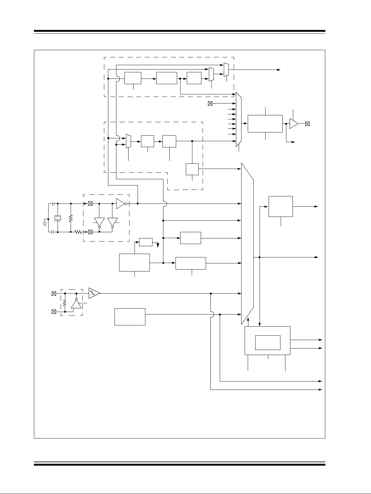
PIC32MX1XX/2XX 28/36/44-PIN FAMILY
Timer1, RTCC
Clock Control Logic
Fail-Safe
Clock
Monitor
FSCM INT
FSCM Event
COSC<2:0>
NOSC<2:0>
OSWEN
FSCMEN<1:0>
PLL
Secondary Oscillator (S
OSC
)
SOSCEN and FSOSCEN
SOSCO
SOSCI
Primary Oscillator (P
OSC
)
P
OSC
(XT, HS, EC)
CPU and Select Peripherals
Peripherals
FRCDIV<2:0>
WDT, PWRT
8 MHz typical
FRC
31.25 kHz typical
FRC
Oscillator
LPRC
Oscillator
S
OSC
LPRC
FRCDIV
TUN<5:0>
div 16
Postscaler
FPLLIDIV<2:0>
PBDIV<1:0>
FRC/16
Postscaler
COSC<2:0>
F
IN
div x
div y
PLLODIV<2:0>
div x
32.768 kHz
PLLMULT<2:0>
PBCLK (T
PB
)
UF
IN
4 MHz
PLL x24
USB Clock (48 MHz)
div 2
UPLLEN
UFRCEN
div x
UPLLIDIV<2:0>
UF
IN
4 MHz FIN 5 MHz
C1
(2)
C2
(2)
XTAL
R
S
(1)
XT
Notes: 1.
A series resistor, RS, may be required for AT strip cut crystals or eliminate clipping. Alternately, to increase oscillator circuit gain,
add a parallel resistor, R
P
, with a value of 1 M
2.
Refer to
Section 6. “Oscillator Configuration”
(DS60001112) in the “
PIC32 Famil y Ref erenc e Ma nual
” for help in determining the
best oscillator components.
3.
The PBCLK out is only available on the OSC2 pin in certain clock modes.
4.
The USB PLL is only available on PIC32MX2XX devices.
OSC2
(3)
OSC1
To Internal
Logic
USB PLL
(4)
div 2
To A DC
SYSCLK
REFCLKI
REFCLKO
OE
To S P I
ROSEL<3:0>
P
OSC
FRC
LPRC
S
OSC
PBCLK
SYSCLK
XTPLL, HSPLL,
ECPLL, FRCPLL
2N
M
512
----------+
RODIV<14:0>
(N)
ROTRIM<8:0>
(M)
R
P
(1)
System PLL
HS
3x 1x
FIGURE 8-1: OSCILLATOR DIAGRAM
DS60001168L-page 78 2011-2019 Microchip Technology Inc.

2011-2019 Microchip Technology Inc. DS60001168L-page 79
8.1 Oscillator Control Regiters
TABLE 8-1: OSCILLATOR CONTROL REGISTER MAP
Bits
(1)
Name
Register
(BF80_#)
Virtual Address
OSCCON
F000
F010 OSCTUN
REFOCON
F020
REFOTRIM
F030
Legend: x = unknown value on Reset; — = unimplemented, read as ‘0’. Reset values are shown in hexadecimal.
Note 1: All registers in this table have corresponding CLR, SET and INV registers at their virtual addresses, plus offsets of 0x4, 0x8 and 0xC, respectively. See Section 11.2 “CLR, SET and INV Registers” for
more information.
2: Reset values are dependent on the DEVCFGx Configuration bits and the type of reset.
3: This bit is only available on PIC32MX2XX devices.
31/15 30/14 29/13 28/12 27/11 26/10 25/9 24/8 23/7 22/6 21/5 20/4 19/3 18/2 17/1 16/0
Bit Range
31:16
31:16
31:16 — RODIV<14:0> 0000
31:16 ROTRIM<8:0>
— — PLLODIV<2:0> FRCDIV<2:0> — SOSCRDY PBDIVRDY PBDIV<1:0> PLLMULT<2:0> x1xx
15:0 —COSC<2:0> — NOSC<2:0> CLKLOCK ULOCK
— — — — — — — — — — — — — — — — 0000
15:0
— — — — — — — — — — TUN<5:0> 0000
15:0 ON
15:0
— — — — — — — —
—SIDL OERSLP— DIVSWEN ACTIVE — — — —
— — — — — — —
—
— — — — — — —
(3)
SLOCK SLPEN CF UFRCEN
(3)
SOSCEN OSWEN xxxx
ROSEL<3:0>
0000
0000
0000
All Resets
(2)
(2)
PIC32MX1XX/2XX 28/36/44-PIN FAMILY

PIC32MX1XX/2XX 28/36/44-PIN FAMILY
REGISTER 8-1: OSCCON: OSCILLATOR CONTROL REGISTER
Bit
Range
31:24
23:16
15:8
7:0
Legend: y = Value set from Configuration bits on POR
R = Readable bit W = Writable bit U = Unimplemented bit, read as ‘0’
-n = Value at POR ‘1’ = Bit is set ‘0’ = Bit is cleared x = Bit is unknown
bit 31-30 Unimplemented: Read as ‘0’
bit 29-27 PLLODIV<2:0>: Output Divider for PLL
bit 26-24 FRCDIV<2:0>: Internal Fast RC (FRC) Oscillator Clock Divider bits
bit 23 Unimplemented: Read as ‘0’
bit 22 SOSCRDY: Secondary Oscillator (S
bit 21 PBDIVRDY: Peripheral Bus Clock (PBCLK) Divisor Ready bit
bit 20-19 PBDIV<1:0>: Peripheral Bus Clock (PBCLK) Divisor bits
Bit
31/23/15/7
U-0 U-0 R/W-y R/W-y R/W-y R/W-0 R/W-0 R/W-1
Bit
30/22/14/6
Bit
29/21/13/5
Bit
28/20/12/4
Bit
27/19/11/3
Bit
26/18/10/2
Bit
25/17/9/1
— — PLLODIV<2:0> FRCDIV<2:0>
U-0 R-0 R-1 R/W-y R/W-y R/W-y R/W-y R/W-y
— SOSCRDY PBDIVRDY PBDIV<1:0> PLLMULT<2:0>
U-0 R-0 R-0 R-0 U-0 R/W-y R/W-y R/W-y
— COSC<2:0> —NOSC<2:0>
R/W-0 R-0 R-0 R/W-0 R/W-0 R/W-0 R/W-y R/W-0
CLKLOCK ULOCK
(1)
SLOCK SLPEN CF UFRCEN
(1)
SOSCEN OSWEN
111 = PLL output divided by 256
110 = PLL output divided by 64
101 = PLL output divided by 32
100 = PLL output divided by 16
011 = PLL output divided by 8
010 = PLL output divided by 4
001 = PLL output divided by 2
000 = PLL output divided by 1
111 = FRC divided by 256
110 = FRC divided by 64
101 = FRC divided by 32
100 = FRC divided by 16
011 = FRC divided by 8
010 = FRC divided by 4
001 = FRC divided by 2 (default setting)
000 = FRC divided by 1
OSC
) Ready Indicator bit
1 = The Secondary Oscillator is running and is stable
0 = The Secondary Oscillator is still warming up or is turned off
1 = PBDIV<1:0> bits can be written
0 = PBDIV<1:0> bits cannot be written
11 = PBCLK is SYSCLK divided by 8 (default)
10 = PBCLK is SYSCLK divided by 4
01 = PBCLK is SYSCLK divided by 2
00 = PBCLK is SYSCLK divided by 1
Bit
24/16/8/0
Note 1: This bit is only available on PIC32MX2XX devices.
Note: Writes to this register require an unlock sequence. Refer to Section 6. “Oscillator” (DS60001112) in the
“PIC32 Family Reference Manual” for details.
DS60001168L-page 80 2011-2019 Microchip Technology Inc.

PIC32MX1XX/2XX 28/36/44-PIN FAMILY
REGISTER 8-1: OSCCON: OSCILLATOR CONTROL REGISTER
bit 18-16 PLLMULT<2:0>: Phase-Locked Loop (PLL) Multiplier bits
111 = Clock is multiplied by 24
110 = Clock is multiplied by 21
101 = Clock is multiplied by 20
100 = Clock is multiplied by 19
011 = Clock is multiplied by 18
010 = Clock is multiplied by 17
001 = Clock is multiplied by 16
000 = Clock is multiplied by 15
bit 15 Unimplemented: Read as ‘0’
bit 14-12 COSC<2:0>: Current Oscillator Selection bits
111 = Internal Fast RC (FRC) Oscillator divided by FRCDIV<2:0> bits (OSCCON<26:24>)
110 = Internal Fast RC (FRC) Oscillator divided by 16
101 = Internal Low-Power RC (LPRC) Oscillator
OSC
100 = Secondary Oscillator (S
011 = Primary Oscillator (P
010 = Primary Oscillator (P
001 = Internal Fast RC Oscillator with PLL module via Postscaler (FRCPLL)
000 = Internal Fast RC (FRC) Oscillator
bit 11 Unimplemented: Read as ‘0’
bit 10-8 NOSC<2:0>: New Oscillator Selection bits
111 = Internal Fast RC Oscillator (FRC) divided by OSCCON<FRCDIV> bits
110 = Internal Fast RC Oscillator (FRC) divided by 16
101 = Internal Low-Power RC (LPRC) Oscillator
100 = Secondary Oscillator (S
011 = Primary Oscillator with PLL module (XTPLL, HSPLL or ECPLL)
010 = Primary Oscillator (XT, HS or EC)
001 = Internal Fast Internal RC Oscillator with PLL module via Postscaler (FRCPLL)
000 = Internal Fast Internal RC Oscillator (FRC)
On Reset, these bits are set to the value of the FNOSC Configuration bits (DEVCFG1<2:0>).
bit 7 CLKLOCK: Clock Selection Lock Enable bit
If clock switching and monitoring is
1 = Clock and PLL selections are locked
0 = Clock and PLL selections are not locked and may be modified
)
OSC
) with PLL module (XTPLL, HSPLL or ECPLL)
OSC
) (XT, HS or EC)
OSC
)
disabled (FCKSM<1:0> = 1x):
If clock switching and monitoring is enabled (FCKSM<1:0> =
Clock and PLL selections are never locked and may be modified.
bit 6 ULOCK: USB PLL Lock Status bit
1 = The USB PLL module is in lock or USB PLL module start-up timer is satisfied
0 =The USB PLL module is out of lock or USB PLL module start-up timer is in progress or the USB PLL is
disabled
bit 5 SLOCK: PLL Lock Status bit
1 = The PLL module is in lock or PLL module start-up timer is satisfied
0 = The PLL module is out of lock, the PLL start-up timer is running, or the PLL is disabled
bit 4 SLPEN: Sleep Mode Enable bit
1 = The device will enter Sleep mode when a WAIT instruction is executed
0 = The device will enter Idle mode when a WAIT instruction is executed
Note 1: This bit is only available on PIC32MX2XX devices.
Note: Writes to this register require an unlock sequence. Refer to Section 6. “Oscillator” (DS60001112) in the
“PIC32 Family Reference Manual” for details.
2011-2019 Microchip Technology Inc. DS60001168L-page 81
(1)
0x):

PIC32MX1XX/2XX 28/36/44-PIN FAMILY
REGISTER 8-1: OSCCON: OSCILLATOR CONTROL REGISTER
bit 3 CF: Clock Fail Detect bit
1 = FSCM has detected a clock failure
0 = No clock failure has been detected
bit 2 UFRCEN: USB FRC Clock Enable bit
1 = Enable the FRC as the clock source for the USB clock source
0 = Use the Primary Oscillator or USB PLL as the USB clock source
bit 1 SOSCEN: Secondary Oscillator (S
1 = Enable the Secondary Oscillator
0 = Disable the Secondary Oscillator
bit 0 OSWEN: Oscillator Switch Enable bit
1 = Initiate an oscillator switch to selection specified by NOSC<2:0> bits
0 = Oscillator switch is complete
Note 1: This bit is only available on PIC32MX2XX devices.
Note: Writes to this register require an unlock sequence. Refer to Section 6. “Oscillator” (DS60001112) in the
“PIC32 Family Reference Manual” for details.
(1)
OSC
) Enable bit
DS60001168L-page 82 2011-2019 Microchip Technology Inc.
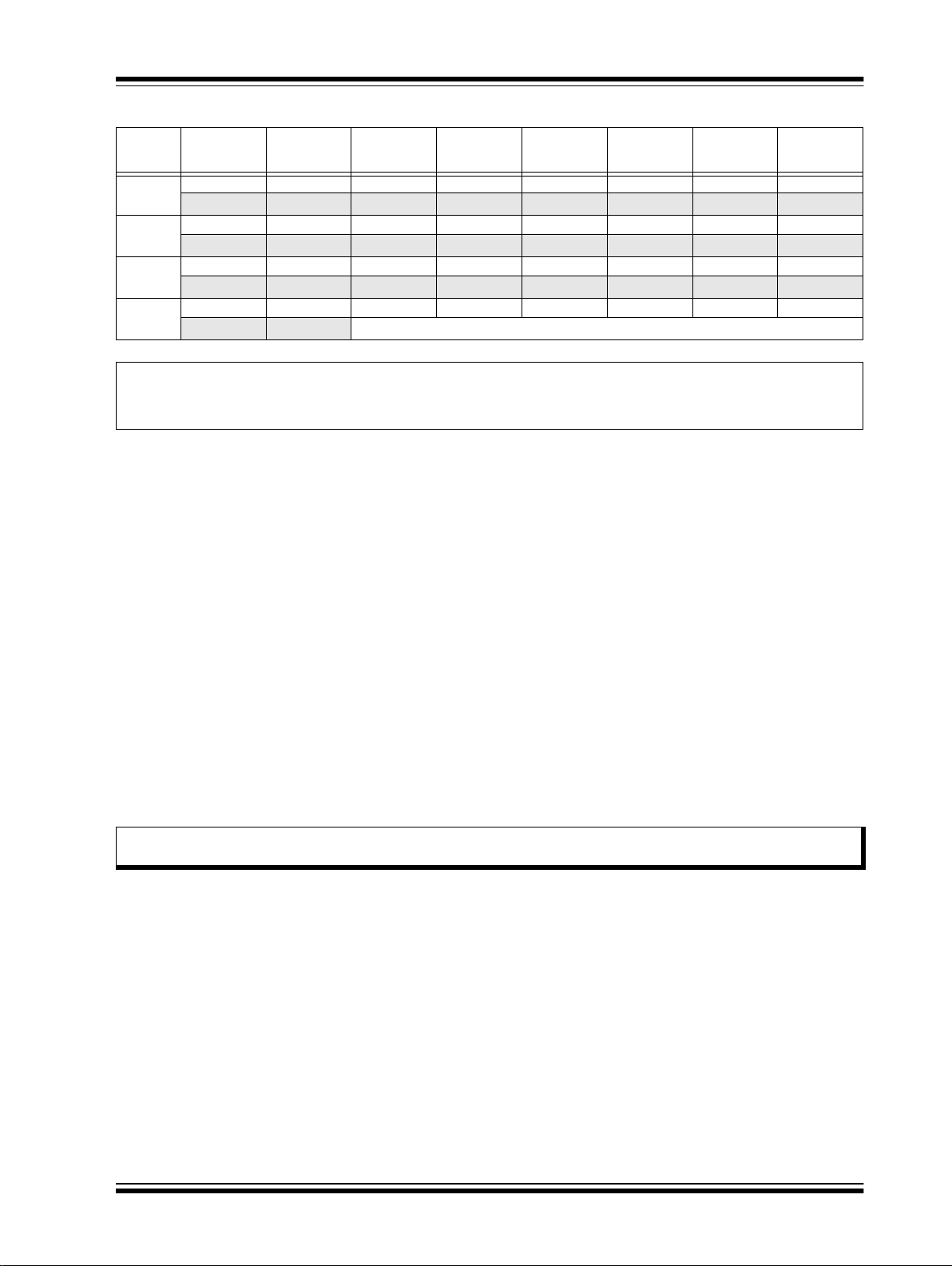
PIC32MX1XX/2XX 28/36/44-PIN FAMILY
REGISTER 8-2: OSCTUN: FRC TUNING REGISTER
Bit
Range
31:24
23:16
15:8
7:0
Legend:
R = Readable bit W = Writable bit U = Unimplemented bit, read as ‘0’
-n = Value at POR ‘1’ = Bit is set ‘0’ = Bit is cleared x = Bit is unknown
bit 31-6 Unimplemented: Read as ‘0’
bit 5-0 TUN<5:0>: FRC Oscillator Tuning bits
Bit
31/23/15/7
U-0 U-0 U-0 U-0 U-0 U-0 U-0 U-0
Bit
30/22/14/6
Bit
29/21/13/5
Bit
28/20/12/4
Bit
27/19/11/3
Bit
26/18/10/2
Bit
25/17/9/1
— — — — — — — —
U-0 R-0 U-0 U-0 U-0 U-0 U-0 U-0
— — — — — — — —
U-0 R-0 U-0 U-0 U-0 U-0 U-0 U-0
— — — — — — — —
U-0 U-0 R/W-0 R/W-0 R/W-0 R/W-0 R/W-0 R/W-0
— — TUN<5:0>
(1)
(1)
100000 = Center frequency -12.5%
100001 =
•
•
•
111111 =
000000 = Center frequency. Oscillator runs at minimal frequency (8 MHz)
000001 =
•
•
•
011110 =
011111 = Center frequency +12.5%
24/16/8/0
Bit
Note 1: OSCTUN functionality has been provided to help customers compensate for temperature effects on the
FRC frequency over a wide range of temperatures. The tuning step size is an approximation, and is neither
characterized, nor tested.
Note: Writes to this register require an unlock sequence. Refer to Section 6. “Oscillator” (DS60001112) in the
“PIC32 Family Reference Manual” for details.
2011-2019 Microchip Technology Inc. DS60001168L-page 83

PIC32MX1XX/2XX 28/36/44-PIN FAMILY
REGISTER 8-3: REFOCON: REFERENCE OSCILLATOR CONTROL REGISTER
Bit
Range
31:24
23:16
15:8
7:0
Legend: HC = Hardware Clearable HS = Hardware Settable
R = Readable bit W = Writable bit U = Unimplemented bit, read as ‘0’
-n = Value at POR ‘1’ = Bit is set ‘0’ = Bit is cleared x = Bit is unknown
Bit
31/23/15/7
U-0 R/W-0 R/W-0 R/W-0 R/W-0 R/W-0 R/W-0 R/W-0
—
R/W-0 R/W-0 R/W-0 R/W-0 R/W-0 R/W-0 R/W-0 R/W-0
R/W-0 U-0 R/W-0 R/W-0 R/W-0 U-0 R/W-0, HC R-0, HS, HC
ON —SIDLOE
U-0 U-0 U-0 U-0 R/W-0 R/W-0 R/W-0 R/W-0
— — — —
Bit
30/22/14/6
Bit
29/21/13/5
Bit
28/20/12/4
RODIV<7:0>
Bit
27/19/11/3
RODIV<14:8>
(1,3)
(2)
RSLP
Bit
26/18/10/2
(1,3)
Bit
25/17/9/1
— DIVSWEN ACTIVE
ROSEL<3:0>
(1)
Bit
24/16/8/0
bit 31 Unimplemented: Read as ‘0’
bit 30-16 RODIV<14:0> Reference Clock Divider bits
(1,3)
The value selects the reference clock divider bits. See Figure 8-1 for information.
bit 15 ON: Output Enable bit
1 = Reference Oscillator module is enabled
0 = Reference Oscillator module is disabled
bit 14 Unimplemented: Read as ‘0’
bit 13 SIDL: Peripheral Stop in Idle Mode bit
1 = Discontinue module operation when the device enters Idle mode
0 = Continue module operation when the device enters Idle mode
bit 12 OE: Reference Clock Output Enable bit
1 = Reference clock is driven out on REFCLKO pin
0 = Reference clock is not driven out on REFCLKO pin
bit 11 RSLP: Reference Oscillator Module Run in Sleep bit
1 = Reference Oscillator module output continues to run in Sleep
0 = Reference Oscillator module output is disabled in Sleep
bit 10 Unimplemented: Read as ‘0’
bit 9 DIVSWEN: Divider Switch Enable bit
1 = Divider switch is in progress
0 = Divider switch is complete
bit 8 ACTIVE: Reference Clock Request Status bit
1 = Reference clock request is active
0 = Reference clock request is not active
bit 7-4 Unimplemented: Read as ‘0’
(2)
Note 1: The ROSEL and RODIV bits should not be written while the ACTIVE bit is ‘1’, as undefined behavior may
result.
2: This bit is ignored when the ROSEL<3:0> bits = 0000 or 0001.
3: While the ON bit is set to ‘1’, writes to these bits do not take effect until the DIVSWEN bit is also set to ’1’.
DS60001168L-page 84 2011-2019 Microchip Technology Inc.

PIC32MX1XX/2XX 28/36/44-PIN FAMILY
REGISTER 8-3: REFOCON: REFERENCE OSCILLATOR CONTROL REGISTER
bit 3-0 ROSEL<3:0>: Reference Clock Source Select bits
1111 = Reserved; do not use
•
•
•
1001 = Reserved; do not use
1000 = REFCLKI
0111 = System PLL output
0110 = USB PLL output
0101 = S
0100 = LPRC
0011 = FRC
0010 = P
0001 = PBCLK
0000 = SYSCLK
Note 1: The ROSEL and RODIV bits should not be written while the ACTIVE bit is ‘1’, as undefined behavior may
result.
2: This bit is ignored when the ROSEL<3:0> bits = 0000 or 0001.
3: While the ON bit is set to ‘1’, writes to these bits do not take effect until the DIVSWEN bit is also set to ’1’.
OSC
OSC
(1)
2011-2019 Microchip Technology Inc. DS60001168L-page 85

PIC32MX1XX/2XX 28/36/44-PIN FAMILY
REGISTER 8-4: REFOTRIM: REFERENCE OSCILLATOR TRIM REGISTER
Bit
Range
31:24
23:16
15:8
7:0
Legend:
R = Readable bit W = Writable bit U = Unimplemented bit, read as ‘0’
-n = Value at POR ‘1’ = Bit is set ‘0’ = Bit is cleared x = Bit is unknown
bit 31-23 ROTRIM<8:0>: Reference Oscillator Trim bits
bit 22-0 Unimplemented: Read as ‘0’
Bit
31/23/15/7
R/W-0 R/W-0 R/W-0 R/W-0 R/W-0 R/W-0 R/W-0 R/W-0
R/W-0 R-0 U-0 U-0 U-0 U-0 U-0 U-0
ROTRIM<0> — — — — — — —
U-0 R-0 U-0 U-0 U-0 U-0 U-0 U-0
— — — — — — — —
U-0 U-0 U-0 U-0 U-0 U-0 U-0 U-0
— — — — — — — —
111111111 = 511/512 divisor added to RODIV value
111111110 = 510/512 divisor added to RODIV value
•
•
•
100000000 = 256/512 divisor added to RODIV value
•
•
•
000000010 = 2/512 divisor added to RODIV value
000000001 = 1/512 divisor added to RODIV value
000000000 = 0/512 divisor added to RODIV value
Bit
30/22/14/6
Bit
29/21/13/5
Bit
28/20/12/4
ROTRIM<8:1>
Bit
27/19/11/3
Bit
26/18/10/2
Bit
25/17/9/1
24/16/8/0
Bit
Note: While the ON (REFOCON<15>) bit is ‘1’, writes to this register do not take effect until the DIVSWEN bit is
also set to ‘1’.
DS60001168L-page 86 2011-2019 Microchip Technology Inc.

PIC32MX1XX/2XX 28/36/44-PIN FAMILY
Address
Channel 0
Channel 1
Channel n
Global Control
(DMACON)
Bus
Channel Priority
Arbitration
S
E
L
S
E
L
Y
I
0
I
1
I
2
I
n
System IRQ
Interrupt
Device Bus and
Peripheral Bus
Control
Control
Control
Interface
Decoder
Controller
Bus Arbitration
9.0 DIRECT MEMORY ACCESS (DMA) CONTROLLER
Note: This data sheet summarizes the features
of the PIC32MX1XX/2XX 28/36/44-pin
Family of devices. It is not intended to be
a comprehensive reference source. To
complement the information in this data
sheet, refer to Section 31. “Direct Mem-
ory Access (DMA) Controller”
(DS60001117), which is available from the
Documentation > Reference Manual
section of the Microchip PIC32 web site
(www.microchip.com/pic32).
The PIC32 Direct Memory Access (DMA) controller is a
bus master module useful for data transfers between
different devices without CPU intervention. The source
and destination of a DMA transfer can be any of the
memory mapped modules existent in the PIC32, such
as Peripheral Bus devices: SPI, UART, PMP, etc., or
memory itself. Figure 9-1 show a block diagram of the
DMA Controller module.
The DMA Controller module has the following key
features:
• Four identical channels, each featuring:
- Auto-increment source and destination
address registers
- Source and destination pointers
- Memory to memory and memory to
peripheral transfers
• Automatic word-size detection:
- Transfer granularity, down to byte level
- Bytes need not be word-aligned at source
and destination
• Fixed priority channel arbitration
• Flexible DMA channel operating modes:
- Manual (software) or automatic (interrupt)
DMA requests
- One-Shot or Auto-Repeat Block Transfer
modes
- Channel-to-channel chaining
• Flexible DMA requests:
- A DMA request can be selected from any of
the peripheral interrupt sources
- Each channel can select any (appropriate)
observable interrupt as its DMA request
source
- A DMA transfer abort can be selected from
any of the peripheral interrupt sources
- Pattern (data) match transfer termination
• Multiple DMA channel status interrupts:
- DMA channel block transfer complete
- Source empty or half empty
- Destination full or half full
- DMA transfer aborted due to an external
event
- Invalid DMA address generated
• DMA debug support features:
- Most recent address accessed by a DMA
channel
- Most recent DMA channel to transfer data
• CRC Generation module:
- CRC module can be assigned to any of the
available channels
- CRC module is highly configurable
FIGURE 9-1: DMA BLOCK DIAGRAM
2011-2019 Microchip Technology Inc. DS60001168L-page 87

DS60001168L-page 88 2011-2019 Microchip Technology Inc.
9.1 DMA Control Registers
TABLE 9-1: DMA GLOBAL REGISTER MAP
Bits
(1)
Name
Register
(BF88_#)
Virtual Address
3000 DMACON
3010 DMASTAT
3020 DMAADDR
Legend: x = unknown value on Reset; — = unimplemented, read as ‘0’. Reset values are shown in hexadecimal.
Note 1: All registers in this table have corresponding CLR, SET and INV registers at its virtual address, plus an offset of 0x4, 0x8 and 0xC, respectively. See Section 11.2 “CLR, SET and INV Registers” for more
information.
TABLE 9-2: DMA CRC REGISTER MAP
(1)
Name
Register
(BF88_#)
Virtual Address
3030 DCRCCON
3040 DCRCDATA
3050 DCRCXOR
Legend: x = unknown value on Reset; — = unimplemented, read as ‘0’. Reset values are shown in hexadecimal.
Note 1: All registers in this table have corresponding CLR, SET and INV registers at their virtual addresses, plus offsets of 0x4, 0x8 and 0xC, respectively. See Section 11.2 “CLR, SET and INV Registers” for
more information.
31/15 30/14 29/13 28/12 27/11 26/10 25/9 24/8 23/7 22/6 21/5 20/4 19/3 18/2 17/1 16/0
Bit Range
31:16
15:0 ON
31:16 — — — — — — — — — — — — — — — — 0000
15:0
31:16
15:0 0000
— — — — — — — — — — — — — — — — 0000
— — SUSPEND DMABUSY — — — — — — — — — — — 0000
— — — — — — — — — — — — RDWR DMACH<2:0>
DMAADDR<31:0>
(2)
0000
0000
Bits
31/15 30/14 29/13 28/12 27/11 26/10 25/9 24/8 23/7 22/6 21/5 20/4 19/3 18/2 17/1 16/0
Bit Range
31:16
15:0 — — — PLEN<4:0> CRCEN CRCAPP CRCTYP — — CRCCH<2:0> 0000
31:16
15:0 0000
31:16
15:0 0000
— —BYTO<1:0>WBO— —BITO— — — — — — — — 0000
DCRCDATA<31:0>
DCRCXOR<31:0>
0000
0000
PIC32MX1XX/2XX 28/36/44-PIN FAMILY
All Resets
All Resets
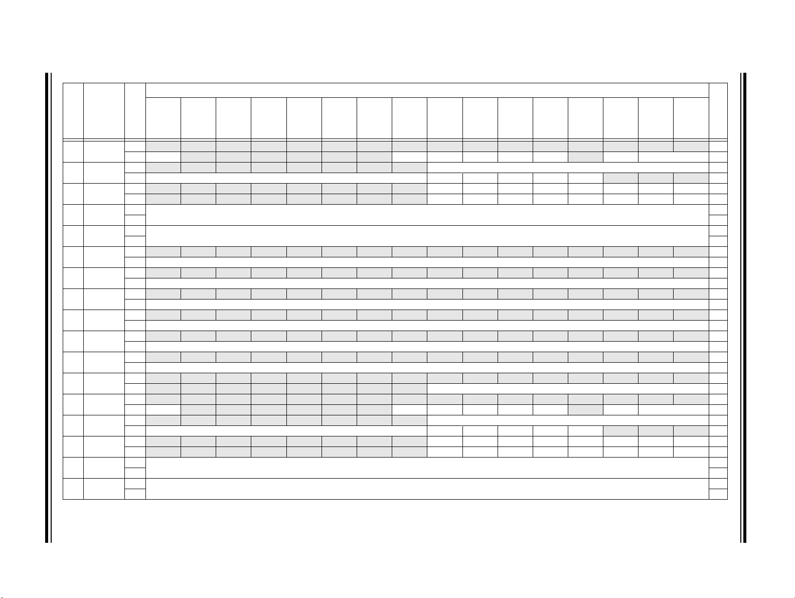
2011-2019 Microchip Technology Inc. DS60001168L-page 89
TABLE 9-3: DMA CHANNELS 0-3 REGISTER MAP
Bits
(1)
Name
Register
(BF88_#)
Virtual Address
3060 DCH0CON
3070 DCH0ECON
3080 DCH0INT
3090 DCH0SSA
30A0 DCH0DSA
30B0 DCH0SSIZ
30C0 DCH0DSIZ
30D0 DCH0SPTR
30E0 DCH0DPTR
30F0 DCH0CSIZ
3100 DCH0CPTR
3110 DCH0DAT
3120 DCH1CON
3130 DCH1ECON
3140 DCH1INT
3150 DCH1SSA
3160 DCH1DSA
Legend: x = unknown value on Reset; — = unimplemented, read as ‘0’. Reset values are shown in hexadecimal.
Note 1: All registers in this table have corresponding CLR, SET and INV registers at their virtual addresses, plus offsets of 0x4, 0x8 and 0xC, respectively. See Section 11.2 “CLR, SET and INV Registers” for
more information.
31/15 30/14 29/13 28/12 27/11 26/10 25/9 24/8 23/7 22/6 21/5 20/4 19/3 18/2 17/1 16/0
Bit Range
31:16
15:0 CHBUSY
31:16 — — — — — — — — CHAIRQ<7:0> 00FF
15:0
31:16 — — — — — — — — CHSDIE CHSHIE CHDDIE CHDHIE CHBCIE CHCCIE CHTAIE CHERIE 0000
15:0
31:16
15:0 0000
31:16
15:0 0000
31:16
15:0 CHSSIZ<15:0> 0000
31:16
15:0 CHDSIZ<15:0> 0000
31:16
15:0 CHSPTR<15:0> 0000
31:16
15:0 CHDPTR<15:0> 0000
31:16
15:0 CHCSIZ<15:0> 0000
31:16
15:0 CHCPTR<15:0> 0000
31:16
15:0
31:16 — — — — — — — — — — — — — — — — 0000
15:0 CHBUSY
31:16 — — — — — — — — CHAIRQ<7:0> 00FF
15:0
31:16 — — — — — — — — CHSDIE CHSHIE CHDDIE CHDHIE CHBCIE CHCCIE CHTAIE CHERIE 0000
15:0
31:16
15:0 0000
31:16
15:0 0000
— — — — — — — — — — — — — — — — 0000
— — — — — — CHCHNS CHEN CHAED CHCHN CHAEN — CHEDET CHPRI<1:0> 0000
CHSIRQ<7:0> CFORCE CABORT PATE N SIRQEN AIRQEN — — — FF00
— — — — — — — — CHSDIF CHSHIF CHDDIF CHDHIF CHBCIF CHCCIF CHTAIF CHERIF 0000
CHSSA<31:0>
CHDSA<31:0>
— — — — — — — — — — — — — — — — 0000
— — — — — — — — — — — — — — — — 0000
— — — — — — — — — — — — — — — — 0000
— — — — — — — — — — — — — — — — 0000
— — — — — — — — — — — — — — — — 0000
— — — — — — — — — — — — — — — — 0000
— — — — — — — — — — — — — — — — 0000
— — — — — — — — CHPDAT<7:0> 0000
— — — — — — CHCHNS CHEN CHAED CHCHN CHAEN — CHEDET CHPRI<1:0> 0000
CHSIRQ<7:0> CFORCE CABORT PATE N SIRQEN AIRQEN — — — FF00
— — — — — — — — CHSDIF CHSHIF CHDDIF CHDHIF CHBCIF CHCCIF CHTAIF CHERIF 0000
CHSSA<31:0>
CHDSA<31:0>
0000
0000
0000
0000
All Resets
PIC32MX1XX/2XX 28/36/44-PIN FAMILY

DS60001168L-page 90 2011-2019 Microchip Technology Inc.
TABLE 9-3: DMA CHANNELS 0-3 REGISTER MAP (CONTINUED)
Bits
(1)
Name
Register
(BF88_#)
Virtual Address
3170 DCH1SSIZ
3180 DCH1DSIZ
3190 DCH1SPTR
31A0 DCH1DPTR
31B0 DCH1CSIZ
31C0 DCH1CPTR
31D0 DCH1DAT
31E0 DCH2CON
31F0 DCH2ECON
3200 DCH2INT
3210 DCH2SSA
3220 DCH2DSA
3230 DCH2SSIZ
3240 DCH2DSIZ
3250 DCH2SPTR
3260 DCH2DPTR
3270 DCH2CSIZ
Legend: x = unknown value on Reset; — = unimplemented, read as ‘0’. Reset values are shown in hexadecimal.
Note 1: All registers in this table have corresponding CLR, SET and INV registers at their virtual addresses, plus offsets of 0x4, 0x8 and 0xC, respectively. See Section 11.2 “CLR, SET and INV Registers” for
more information.
31/15 30/14 29/13 28/12 27/11 26/10 25/9 24/8 23/7 22/6 21/5 20/4 19/3 18/2 17/1 16/0
Bit Range
31:16
15:0 CHSSIZ<15:0> 0000
31:16
15:0 CHDSIZ<15:0> 0000
31:16
15:0 CHSPTR<15:0> 0000
31:16
15:0 CHDPTR<15:0> 0000
31:16
15:0 CHCSIZ<15:0> 0000
31:16
15:0 CHCPTR<15:0> 0000
31:16
15:0
31:16 — — — — — — — — — — — — — — — — 0000
15:0 CHBUSY
31:16 — — — — — — — — CHAIRQ<7:0> 00FF
15:0
31:16 — — — — — — — — CHSDIE CHSHIE CHDDIE CHDHIE CHBCIE CHCCIE CHTAIE CHERIE 0000
15:0
31:16
15:0 0000
31:16
15:0 0000
31:16
15:0 CHSSIZ<15:0> 0000
31:16
15:0 CHDSIZ<15:0> 0000
31:16
15:0 CHSPTR<15:0> 0000
31:16
15:0 CHDPTR<15:0> 0000
31:16
15:0 CHCSIZ<15:0> 0000
— — — — — — — — — — — — — — — — 0000
— — — — — — — — — — — — — — — — 0000
— — — — — — — — — — — — — — — — 0000
— — — — — — — — — — — — — — — — 0000
— — — — — — — — — — — — — — — — 0000
— — — — — — — — — — — — — — — — 0000
— — — — — — — — — — — — — — — — 0000
— — — — — — — — CHPDAT<7:0> 0000
— — — — — — CHCHNS CHEN CHAED CHCHN CHAEN — CHEDET CHPRI<1:0> 0000
CHSIRQ<7:0> CFORCE CABORT PATE N SIRQEN AIRQEN — — — FF00
— — — — — — — — CHSDIF CHSHIF CHDDIF CHDHIF CHBCIF CHCCIF CHTAIF CHERIF 0000
CHSSA<31:0>
CHDSA<31:0>
— — — — — — — — — — — — — — — — 0000
— — — — — — — — — — — — — — — — 0000
— — — — — — — — — — — — — — — — 0000
— — — — — — — — — — — — — — — — 0000
— — — — — — — — — — — — — — — — 0000
0000
0000
PIC32MX1XX/2XX 28/36/44-PIN FAMILY
All Resets

2011-2019 Microchip Technology Inc. DS60001168L-page 91
TABLE 9-3: DMA CHANNELS 0-3 REGISTER MAP (CONTINUED)
Bits
(1)
Name
Register
(BF88_#)
Virtual Address
3280 DCH2CPTR
3290 DCH2DAT
32A0 DCH3CON
32B0 DCH3ECON
32C0 DCH3INT
32D0 DCH3SSA
32E0 DCH3DSA
32F0 DCH3SSIZ
3300 DCH3DSIZ
3310 DCH3SPTR
3320 DCH3DPTR
3330 DCH3CSIZ
3340 DCH3CPTR
3350 DCH3DAT
Legend: x = unknown value on Reset; — = unimplemented, read as ‘0’. Reset values are shown in hexadecimal.
Note 1: All registers in this table have corresponding CLR, SET and INV registers at their virtual addresses, plus offsets of 0x4, 0x8 and 0xC, respectively. See Section 11.2 “CLR, SET and INV Registers” for
more information.
31/15 30/14 29/13 28/12 27/11 26/10 25/9 24/8 23/7 22/6 21/5 20/4 19/3 18/2 17/1 16/0
Bit Range
31:16
15:0 CHCPTR<15:0> 0000
31:16
15:0
31:16
15:0 CHBUSY
31:16 — — — — — — — — CHAIRQ<7:0> 00FF
15:0
31:16 — — — — — — — — CHSDIE CHSHIE CHDDIE CHDHIE CHBCIE CHCCIE CHTAIE CHERIE 0000
15:0
31:16
15:0 0000
31:16
15:0 0000
31:16
15:0 CHSSIZ<15:0> 0000
31:16
15:0 CHDSIZ<15:0> 0000
31:16
15:0 CHSPTR<15:0> 0000
31:16
15:0 CHDPTR<15:0> 0000
31:16
15:0 CHCSIZ<15:0> 0000
31:16
15:0 CHCPTR<15:0> 0000
31:16
15:0
— — — — — — — — — — — — — — — — 0000
— — — — — — — — — — — — — — — — 0000
— — — — — — — — CHPDAT<7:0> 0000
— — — — — — — — — — — — — — — — 0000
— — — — — — CHCHNS CHEN CHAED CHCHN CHAEN — CHEDET CHPRI<1:0> 0000
CHSIRQ<7:0> CFORCE CABORT PATE N SIRQEN AIRQEN — — — FF00
— — — — — — — — CHSDIF CHSHIF CHDDIF CHDHIF CHBCIF CHCCIF CHTAIF CHERIF 0000
CHSSA<31:0>
CHDSA<31:0>
— — — — — — — — — — — — — — — — 0000
— — — — — — — — — — — — — — — — 0000
— — — — — — — — — — — — — — — — 0000
— — — — — — — — — — — — — — — — 0000
— — — — — — — — — — — — — — — — 0000
— — — — — — — — — — — — — — — — 0000
— — — — — — — — — — — — — — — — 0000
— — — — — — — — CHPDAT<7:0> 0000
0000
0000
All Resets
PIC32MX1XX/2XX 28/36/44-PIN FAMILY

PIC32MX1XX/2XX 28/36/44-PIN FAMILY
REGISTER 9-1: DMACON: DMA CONTROLLER CONTROL REGISTER
Bit
Range
31:24
23:16
15:8
7:0
Legend:
R = Readable bit W = Writable bit U = Unimplemented bit, read as ‘0’
-n = Value at POR ‘1’ = Bit is set ‘0’ = Bit is cleared x = Bit is unknown
bit 31-16 Unimplemented: Read as ‘0’
bit 15 ON: DMA On bit
bit 14-13 Unimplemented: Read as ‘0’
bit 12 SUSPEND: DMA Suspend bit
bit 11 DMABUSY: DMA Module Busy bit
bit 10-0 Unimplemented: Read as ‘0’
Bit
31/23/15/7
U-0 U-0 U-0 U-0 U-0 U-0 U-0 U-0
Bit
30/22/14/6
Bit
29/21/13/5
Bit
28/20/12/4
Bit
27/19/11/3
Bit
26/18/10/2
Bit
25/17/9/1
— — — — — — — —
U-0 U-0 U-0 U-0 U-0 U-0 U-0 U-0
— — — — — — — —
R/W-0 U-0 U-0 R/W-0 R/W-0 U-0 U-0 U-0
(1)
ON
U-0 U-0 U-0 U-0 U-0 U-0 U-0 U-0
— — SUSPEND DMABUSY — — —
— — — — — — — —
(1)
1 = DMA module is enabled
0 = DMA module is disabled
1 = DMA transfers are suspended to allow CPU uninterrupted access to data bus
0 = DMA operates normally
1 = DMA module is active
0 = DMA module is disabled and not actively transferring data
24/16/8/0
Bit
Note 1: When using 1:1 PBCLK divisor, the user’s software should not read/write the peripheral’s SFRs in the
SYSCLK cycle immediately following the instruction that clears the module’s ON bit.
DS60001168L-page 92 2011-2019 Microchip Technology Inc.
PIC32MX1XX/2XX 28/36/44-PIN FAMILY
REGISTER 9-2: DMASTAT: DMA STATUS REGISTER
Bit
Range
31:24
23:16
15:8
7:0
Legend:
R = Readable bit W = Writable bit U = Unimplemented bit, read as ‘0’
-n = Value at POR ‘1’ = Bit is set ‘0’ = Bit is cleared x = Bit is unknown
bit 31-4 Unimplemented: Read as ‘0’
bit 3 RDWR: Read/Write Status bit
bit 2-0 DMACH<2:0>: DMA Channel bits
Bit
31/23/15/7
U-0 U-0 U-0 U-0 U-0 U-0 U-0 U-0
Bit
30/22/14/6
Bit
29/21/13/5
Bit
28/20/12/4
Bit
27/19/11/3
Bit
26/18/10/2
Bit
25/17/9/1
— — — — — — — —
U-0 U-0 U-0 U-0 U-0 U-0 U-0 U-0
— — — — — — — —
U-0 U-0 U-0 U-0 U-0 U-0 U-0 U-0
— — — — — — — —
U-0 U-0 U-0 U-0 R-0 R-0 R-0 R-0
— — — — RDWR DMACH<2:0>
1 = Last DMA bus access was a read
0 = Last DMA bus access was a write
These bits contain the value of the most recent active DMA channel.
24/16/8/0
Bit
REGISTER 9-3: DMAADDR: DMA ADDRESS REGISTER
Bit
Range
31:24
23:16
15:8
7:0
Legend:
R = Readable bit W = Writable bit U = Unimplemented bit, read as ‘0’
-n = Value at POR ‘1’ = Bit is set ‘0’ = Bit is cleared x = Bit is unknown
bit 31-0 DMAADDR<31:0>: DMA Module Address bits
Bit
31/23/15/7
R-0 R-0 R-0 R-0 R-0 R-0 R-0 R-0
Bit
30/22/14/6
Bit
29/21/13/5
Bit
28/20/12/4
Bit
27/19/11/3
Bit
26/18/10/2
Bit
25/17/9/1
DMAADDR<31:24>
R-0 R-0 R-0 R-0 R-0 R-0 R-0 R-0
DMAADDR<23:16>
R-0 R-0 R-0 R-0 R-0 R-0 R-0 R-0
DMAADDR<15:8>
R-0 R-0 R-0 R-0 R-0 R-0 R-0 R-0
DMAADDR<7:0>
These bits contain the address of the most recent DMA access.
24/16/8/0
Bit
2011-2019 Microchip Technology Inc. DS60001168L-page 93

PIC32MX1XX/2XX 28/36/44-PIN FAMILY
REGISTER 9-4: DCRCCON: DMA CRC CONTROL REGISTER
Bit
Range
31:24
23:16
15:8
7:0
Legend:
R = Readable bit W = Writable bit U = Unimplemented bit, read as ‘0’
-n = Value at POR ‘1’ = Bit is set ‘0’ = Bit is cleared x = Bit is unknown
bit 31-30 Unimplemented: Read as ‘0’
bit 29-28 BYTO<1:0>: CRC Byte Order Selection bits
bit 27 WBO: CRC Write Byte Order Selection bit
bit 26-25 Unimplemented: Read as ‘0’
bit 24 BITO: CRC Bit Order Selection bit
Bit
31/23/15/7
U-0 U-0 R/W-0 R/W-0 R/W-0 U-0 U-0 R/W-0
— — BYTO<1:0> WBO
U-0 U-0 U-0 U-0 U-0 U-0 U-0 U-0
Bit
30/22/14/6
Bit
29/21/13/5
Bit
28/20/12/4
Bit
27/19/11/3
(1)
Bit
26/18/10/2
Bit
25/17/9/1
24/16/8/0
— —BITO
— — — — — — — —
U-0 U-0 U-0 R/W-0 R/W-0 R/W-0 R/W-0 R/W-0
— — — PLEN<4:0>
R/W-0 R/W-0 R/W-0 U-0 U-0 R/W-0 R/W-0 R/W-0
CRCEN CRCAPP
(1)
CRCTYP — — CRCCH<2:0>
11 = Endian byte swap on half-word boundaries (i.e., source half-word order with reverse source byte order
per half-word)
10 = Swap half-words on word boundaries (i.e., reverse source half-word order with source byte order per
half-word)
01 = Endian byte swap on word boundaries (i.e., reverse source byte order)
00 = No swapping (i.e., source byte order)
(1)
1 = Source data is written to the destination re-ordered as defined by BYTO<1:0>
0 = Source data is written to the destination unaltered
When CRCTYP (DCRCCON<15>) =
1 (CRC module is in IP Header mode):
1 = The IP header checksum is calculated Least Significant bit (LSb) first (i.e., reflected)
0 = The IP header checksum is calculated Most Significant bit (MSb) first (i.e., not reflected)
Bit
When CRCTYP (DCRCCON<15>) =
0 (CRC module is in LFSR mode):
1 = The LFSR CRC is calculated Least Significant bit first (i.e., reflected)
0 = The LFSR CRC is calculated Most Significant bit first (i.e., not reflected)
bit 23-13 Unimplemented: Read as ‘0’
bit 12-8 PLEN<4:0>: Polynomial Length bits
When CRCTYP (DCRCCON<15>) =
1 (CRC module is in IP Header mode):
These bits are unused.
When CRCTYP (DCRCCON<15>) =
0 (CRC module is in LFSR mode):
Denotes the length of the polynomial – 1.
bit 7 CRCEN: CRC Enable bit
1 = CRC module is enabled and channel transfers are routed through the CRC module
0 = CRC module is disabled and channel transfers proceed normally
Note 1: When WBO = 1, unaligned transfers are not supported and the CRCAPP bit cannot be set.
DS60001168L-page 94 2011-2019 Microchip Technology Inc.

PIC32MX1XX/2XX 28/36/44-PIN FAMILY
REGISTER 9-4: DCRCCON: DMA CRC CONTROL REGISTER (CONTINUED)
bit 6 CRCAPP: CRC Append Mode bit
1 = The DMA transfers data from the source into the CRC but NOT to the destination. When a block transfer
completes the DMA writes the calculated CRC value to the location given by CHxDSA
0 = The DMA transfers data from the source through the CRC obeying WBO as it writes the data to the
destination
bit 5 CRCTYP: CRC Type Selection bit
1 = The CRC module will calculate an IP header checksum
0 = The CRC module will calculate a LFSR CRC
bit 4-3 Unimplemented: Read as ‘0’
bit 2-0 CRCCH<2:0>: CRC Channel Select bits
111 = CRC is assigned to Channel 7
110 = CRC is assigned to Channel 6
101 = CRC is assigned to Channel 5
100 = CRC is assigned to Channel 4
011 = CRC is assigned to Channel 3
010 = CRC is assigned to Channel 2
001 = CRC is assigned to Channel 1
000 = CRC is assigned to Channel 0
Note 1: When WBO = 1, unaligned transfers are not supported and the CRCAPP bit cannot be set.
(1)
2011-2019 Microchip Technology Inc. DS60001168L-page 95
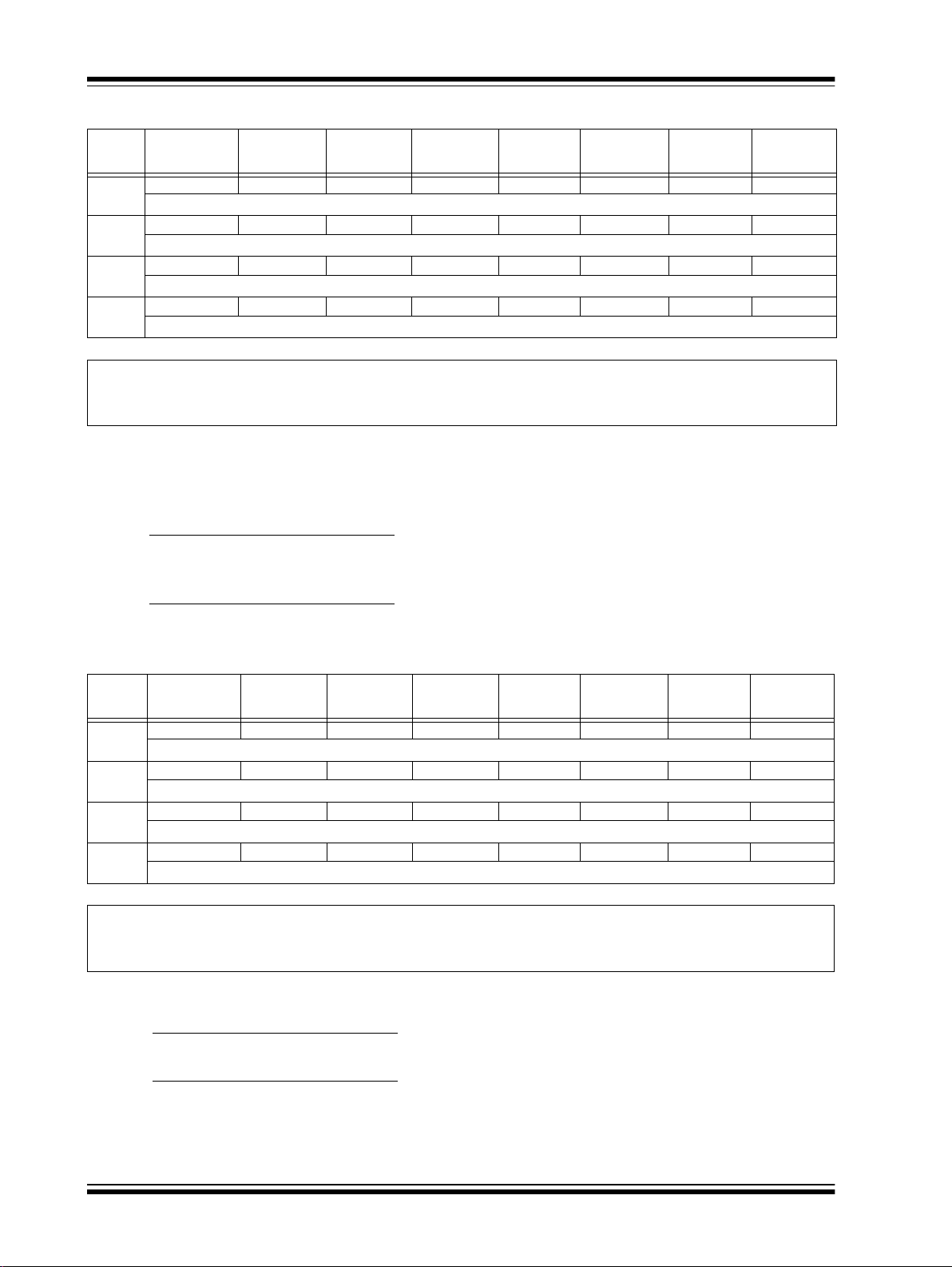
PIC32MX1XX/2XX 28/36/44-PIN FAMILY
REGISTER 9-5: DCRCDATA: DMA CRC DATA REGISTER
Bit
Range
31:24
23:16
15:8
7:0
Legend:
R = Readable bit W = Writable bit U = Unimplemented bit, read as ‘0’
-n = Value at POR ‘1’ = Bit is set ‘0’ = Bit is cleared x = Bit is unknown
bit 31-0 DCRCDATA<31:0>: CRC Data Register bits
Bit
31/23/15/7
R/W-0 R/W-0 R/W-0 R/W-0 R/W-0 R/W-0 R/W-0 R/W-0
Bit
30/22/14/6
Bit
29/21/13/5
Bit
28/20/12/4
Bit
27/19/11/3
Bit
26/18/10/2
Bit
25/17/9/1
24/16/8/0
DCRCDATA<31:24>
R/W-0 R/W-0 R/W-0 R/W-0 R/W-0 R/W-0 R/W-0 R/W-0
DCRCDATA<23:16>
R/W-0 R/W-0 R/W-0 R/W-0 R/W-0 R/W-0 R/W-0 R/W-0
DCRCDATA<15:8>
R/W-0 R/W-0 R/W-0 R/W-0 R/W-0 R/W-0 R/W-0 R/W-0
DCRCDATA<7:0>
Writing to this register will seed the CRC generator. Reading from this register will return the current value of
the CRC. Bits greater than PLEN will return ‘0’ on any read.
Bit
When CRCTYP (DCRCCON<15>) =
1 (CRC module is in IP Header mode):
Only the lower 16 bits contain IP header checksum information. The upper 16 bits are always ‘0’. Data written
to this register is converted and read back in 1’s complement form (i.e., current IP header checksum value).
When CRCTYP (DCRCCON<15>) =
0 (CRC module is in LFSR mode):
Bits greater than PLEN will return ‘0’ on any read.
REGISTER 9-6: DCRCXOR: DMA CRCXOR ENABLE REGISTER
Bit
Range
31:24
23:16
15:8
7:0
Legend:
R = Readable bit W = Writable bit U = Unimplemented bit, read as ‘0’
-n = Value at POR ‘1’ = Bit is set ‘0’ = Bit is cleared x = Bit is unknown
Bit
31/23/15/7
R/W-0 R/W-0 R/W-0 R/W-0 R/W-0 R/W-0 R/W-0 R/W-0
Bit
30/22/14/6
Bit
29/21/13/5
Bit
28/20/12/4
Bit
27/19/11/3
Bit
26/18/10/2
Bit
25/17/9/1
DCRCXOR<31:24>
R/W-0 R/W-0 R/W-0 R/W-0 R/W-0 R/W-0 R/W-0 R/W-0
DCRCXOR<23:16>
R/W-0 R/W-0 R/W-0 R/W-0 R/W-0 R/W-0 R/W-0 R/W-0
DCRCXOR<15:8>
R/W-0 R/W-0 R/W-0 R/W-0 R/W-0 R/W-0 R/W-0 R/W-0
DCRCXOR<7:0>
24/16/8/0
Bit
bit 31-0 DCRCXOR<31:0>: CRC XOR Register bits
When CRCTYP (DCRCCON<15>) =
1 (CRC module is in IP Header mode):
This register is unused.
When CRCTYP (DCRCCON<15>) =
0 (CRC module is in LFSR mode):
1 = Enable the XOR input to the Shift register
0 = Disable the XOR input to the Shift register; data is shifted in directly from the previous stage in
the register
DS60001168L-page 96 2011-2019 Microchip Technology Inc.

PIC32MX1XX/2XX 28/36/44-PIN FAMILY
REGISTER 9-7: DCHxCON: DMA CHANNEL ‘x’ CONTROL REGISTER
Bit
Range
31:24
23:16
15:8
7:0
Legend:
R = Readable bit W = Writable bit U = Unimplemented bit, read as ‘0’
-n = Value at POR ‘1’ = Bit is set ‘0’ = Bit is cleared x = Bit is unknown
bit 31-16 Unimplemented: Read as ‘0’
bit 15 CHBUSY: Channel Busy bit
bit 14-9 Unimplemented: Read as ‘0’
bit 8 CHCHNS: Chain Channel Selection bit
bit 7 CHEN: Channel Enable bit
bit 6 CHAED: Channel Allow Events If Disabled bit
bit CHCHN: Channel Chain Enable bit
bit 4 CHAEN: Channel Automatic Enable bit
bit 3 Unimplemented: Read as ‘0’
bit 2 CHEDET: Channel Event Detected bit
bit 1-0 CHPRI<1:0>: Channel Priority bits
Bit
31/23/15/7
U-0 U-0 U-0 U-0 U-0 U-0 U-0 U-0
Bit
30/22/14/6
Bit
29/21/13/5
Bit
28/20/12/4
Bit
27/19/11/3
Bit
26/18/10/2
Bit
25/17/9/1
24/16/8/0
— — — — — — — —
U-0 U-0 U-0 U-0 U-0 U-0 U-0 U-0
— — — — — — — —
R/W-0 U-0 U-0 U-0 U-0 U-0 U-0 R/W-0
CHBUSY — — — — — — CHCHNS
R/W-0 R/W-0 R/W-0 R/W-0 U-0 R-0 R/W-0 R/W-0
(2)
CHEN
CHAED CHCHN CHAEN — CHEDET CHPRI<1:0>
1 = Channel is active or has been enabled
0 = Channel is inactive or has been disabled
(1)
1 = Chain to channel lower in natural priority (CH1 will be enabled by CH2 transfer complete)
0 = Chain to channel higher in natural priority (CH1 will be enabled by CH0 transfer complete)
(2)
1 = Channel is enabled
0 = Channel is disabled
1 = Channel start/abort events will be registered, even if the channel is disabled
0 = Channel start/abort events will be ignored if the channel is disabled
1 = Allow channel to be chained
0 = Do not allow channel to be chained
1 = Channel is continuously enabled, and not automatically disabled after a block transfer is complete
0 = Channel is disabled on block transfer complete
1 = An event has been detected
0 = No events have been detected
11 = Channel has priority 3 (highest)
10 = Channel has priority 2
01 = Channel has priority 1
00 = Channel has priority 0
Bit
(1)
Note 1: The chain selection bit takes effect when chaining is enabled (i.e., CHCHN = 1).
2: When the channel is suspended by clearing this bit, the user application should poll the CHBUSY bit (if
available on the device variant) to see when the channel is suspended, as it may take some clock cycles
to complete a current transaction before the channel is suspended.
2011-2019 Microchip Technology Inc. DS60001168L-page 97
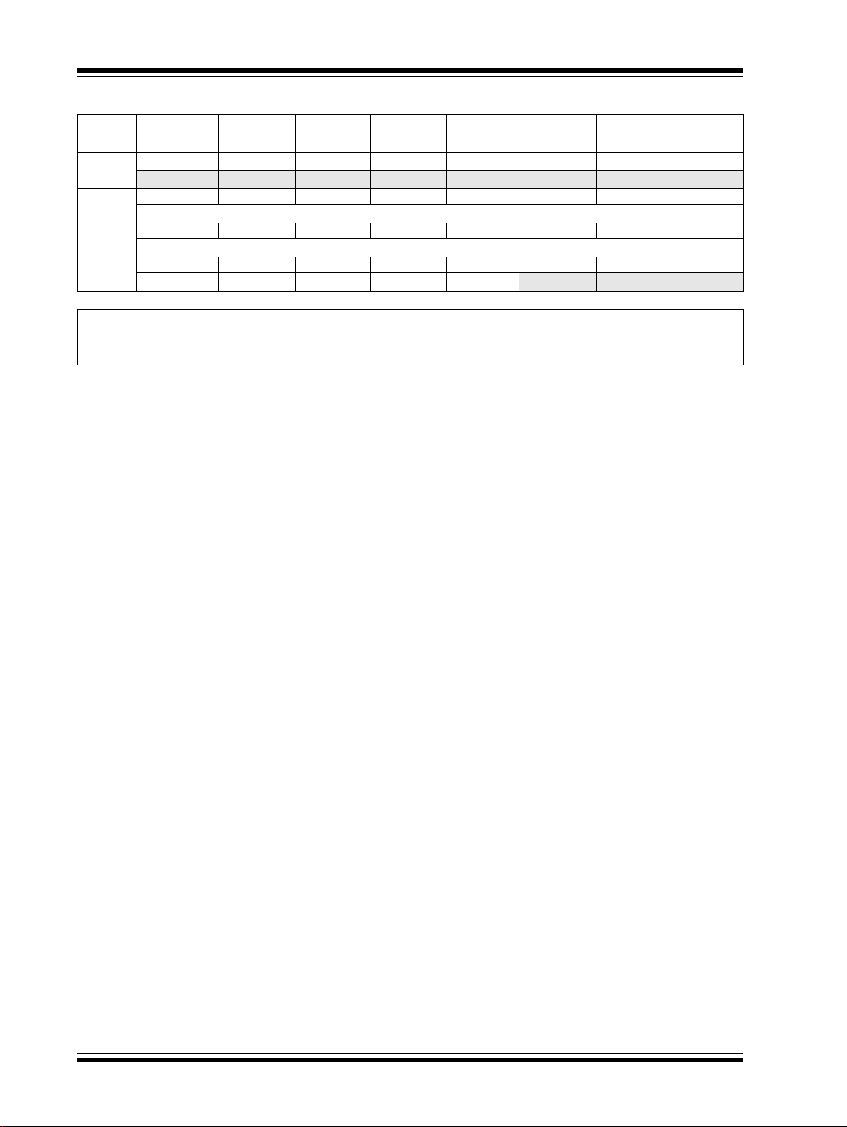
PIC32MX1XX/2XX 28/36/44-PIN FAMILY
REGISTER 9-8: DCHxECON: DMA CHANNEL ‘x’ EVENT CONTROL REGISTER
Bit
Range
31:24
23:16
15:8
7:0
Legend: S = Settable bit
R = Readable bit W = Writable bit U = Unimplemented bit, read as ‘0’
-n = Value at POR ‘1’ = Bit is set ‘0’ = Bit is cleared x = Bit is unknown
Bit
31/23/15/7
U-0 U-0 U-0 U-0 U-0 U-0 U-0 U-0
Bit
30/22/14/6
Bit
29/21/13/5
Bit
28/20/12/4
Bit
27/19/11/3
Bit
26/18/10/2
Bit
25/17/9/1
24/16/8/0
— — — — — — — —
R/W-1 R/W-1 R/W-1 R/W-1 R/W-1 R/W-1 R/W-1 R/W-1
CHAIRQ<7:0>
R/W-1 R/W-1 R/W-1 R/W-1 R/W-1 R/W-1 R/W-1 R/W-1
CHSIRQ<7:0>
S-0 S-0 R/W-0 R/W-0 R/W-0 U-0 U-0 U-0
(1)
(1)
CFORCE CABORT PATEN SIRQEN AIRQEN — — —
Bit
bit 31-24 Unimplemented: Read as ‘0’
bit 23-16 CHAIRQ<7:0>: Channel Transfer Abort IRQ bits
11111111 = Interrupt 255 will abort any transfers in progress and set CHAIF flag
•
•
•
00000001 = Interrupt 1 will abort any transfers in progress and set CHAIF flag
00000000 = Interrupt 0 will abort any transfers in progress and set CHAIF flag
bit 15-8 CHSIRQ<7:0>: Channel Transfer Start IRQ bits
11111111 = Interrupt 255 will initiate a DMA transfer
•
•
•
00000001 = Interrupt 1 will initiate a DMA transfer
00000000 = Interrupt 0 will initiate a DMA transfer
bit 7 CFORCE: DMA Forced Transfer bit
1 = A DMA transfer is forced to begin when this bit is written to a ‘1’
0 = This bit always reads ‘0’
bit 6 CABORT: DMA Abort Transfer bit
1 = A DMA transfer is aborted when this bit is written to a ‘1’
0 = This bit always reads ‘0’
bit 5 PATE N: Channel Pattern Match Abort Enable bit
1 = Abort transfer and clear CHEN on pattern match
0 = Pattern match is disabled
bit 4 SIRQEN: Channel Start IRQ Enable bit
1 = Start channel cell transfer if an interrupt matching CHSIRQ occurs
0 = Interrupt number CHSIRQ is ignored and does not start a transfer
bit 3 AIRQEN: Channel Abort IRQ Enable bit
1 = Channel transfer is aborted if an interrupt matching CHAIRQ occurs
0 = Interrupt number CHAIRQ is ignored and does not terminate a transfer
bit 2-0 Unimplemented: Read as ‘0’
(1)
(1)
Note 1: See Table 7-1: “Interrupt IRQ, Vector and Bit Location” for the list of available interrupt IRQ sources.
DS60001168L-page 98 2011-2019 Microchip Technology Inc.

PIC32MX1XX/2XX 28/36/44-PIN FAMILY
REGISTER 9-9: DCHxINT: DMA CHANNEL ‘x’ INTERRUPT CONTROL REGISTER
Bit
Range
31:24
23:16
15:8
7:0
Legend:
R = Readable bit W = Writable bit U = Unimplemented bit, read as ‘0’
-n = Value at POR ‘1’ = Bit is set ‘0’ = Bit is cleared x = Bit is unknown
bit 31-24 Unimplemented: Read as ‘0’
bit 23 CHSDIE: Channel Source Done Interrupt Enable bit
bit 22 CHSHIE: Channel Source Half Empty Interrupt Enable bit
bit 21 CHDDIE: Channel Destination Done Interrupt Enable bit
bit 20 CHDHIE: Channel Destination Half Full Interrupt Enable bit
bit 19 CHBCIE: Channel Block Transfer Complete Interrupt Enable bit
bit 18 CHCCIE: Channel Cell Transfer Complete Interrupt Enable bit
bit 17 CHTAIE: Channel Transfer Abort Interrupt Enable bit
bit 16 CHERIE: Channel Address Error Interrupt Enable bit
bit 15-8 Unimplemented: Read as ‘0’
bit 7 CHSDIF: Channel Source Done Interrupt Flag bit
bit 6 CHSHIF: Channel Source Half Empty Interrupt Flag bit
bit 5 CHDDIF: Channel Destination Done Interrupt Flag bit
Bit
31/23/15/7
U-0 U-0 U-0 U-0 U-0 U-0 U-0 U-0
— — — — — — — —
R/W-0 R/W-0 R/W-0 R/W-0 R/W-0 R/W-0 R/W-0 R/W-0
CHSDIE CHSHIE CHDDIE CHDHIE CHBCIE CHCCIE CHTAIE CHERIE
U-0 U-0 U-0 U-0 U-0 U-0 U-0 U-0
— — — — — — — —
R/W-0 R/W-0 R/W-0 R/W-0 R/W-0 R/W-0 R/W-0 R/W-0
CHSDIF CHSHIF CHDDIF CHDHIF CHBCIF CHCCIF CHTAIF CHERIF
1 = Interrupt is enabled
0 = Interrupt is disabled
1 = Interrupt is enabled
0 = Interrupt is disabled
1 = Interrupt is enabled
0 = Interrupt is disabled
1 = Interrupt is enabled
0 = Interrupt is disabled
1 = Interrupt is enabled
0 = Interrupt is disabled
1 = Interrupt is enabled
0 = Interrupt is disabled
1 = Interrupt is enabled
0 = Interrupt is disabled
1 = Interrupt is enabled
0 = Interrupt is disabled
1 = Channel Source Pointer has reached end of source (CHSPTR = CHSSIZ)
0 = No interrupt is pending
1 = Channel Source Pointer has reached midpoint of source (CHSPTR =CHSSIZ/2)
0 = No interrupt is pending
1 = Channel Destination Pointer has reached end of destination (CHDPTR = CHDSIZ)
0 = No interrupt is pending
Bit
30/22/14/6
Bit
29/21/13/5
Bit
28/20/12/4
Bit
27/19/11/3
Bit
26/18/10/2
Bit
25/17/9/1
24/16/8/0
Bit
2011-2019 Microchip Technology Inc. DS60001168L-page 99

PIC32MX1XX/2XX 28/36/44-PIN FAMILY
REGISTER 9-9: DCHxINT: DMA CHANNEL ‘x’ INTERRUPT CONTROL REGISTER (CONTINUED)
bit 4 CHDHIF: Channel Destination Half Full Interrupt Flag bit
1 = Channel Destination Pointer has reached midpoint of destination (CHDPTR = CHDSIZ/2)
0 = No interrupt is pending
bit 3 CHBCIF: Channel Block Transfer Complete Interrupt Flag bit
1 = A block transfer has been completed (the larger of CHSSIZ/CHDSIZ bytes has been transferred), or a
pattern match event occurs
0 = No interrupt is pending
bit 2 CHCCIF: Channel Cell Transfer Complete Interrupt Flag bit
1 = A cell transfer has been completed (CHCSIZ bytes have been transferred)
0 = No interrupt is pending
bit 1 CHTAIF: Channel Transfer Abort Interrupt Flag bit
1 = An interrupt matching CHAIRQ has been detected and the DMA transfer has been aborted
0 = No interrupt is pending
bit 0 CHERIF: Channel Address Error Interrupt Flag bit
1 = A channel address error has been detected (either the source or the destination address is invalid)
0 = No interrupt is pending
DS60001168L-page 100 2011-2019 Microchip Technology Inc.
 Loading...