


PIC18F87K90 Family
Data Sheet
64/80-Pin, High-Performance
Microcontrollers with LCD Driver and
nanoWatt XLP Technology
2011 Microchip Technology Inc. DS39957C

Note the following details of the code protection feature on Microchip devices:
• Microchip products meet the specification contained in their particular Microchip Data Sheet.
• Microchip believes that its family of products is one of the most secure families of its kind on the market today, when used in the
intended manner and under normal conditions.
• There are dishonest and possibly illegal methods used to breach the code protection feature. All of these methods, to our
knowledge, require using the Microchip products in a manner outside the operating specifications contained in Microchip’s Data
Sheets. Most likely, the person doing so is engaged in theft of intellectual property.
• Microchip is willing to work with the customer who is concerned about the integrity of their code.
• Neither Microchip nor any other semiconductor manufacturer can guarantee the security of their code. Code protection does not
mean that we are guaranteeing the product as “unbreakable.”
Code protection is constantly evolving. We at Microchip are committed to continuously improving the code protection features of our
products. Attempts to break Microchip’s code protection feature may be a violation of the Digital Millennium Copyright Act. If such acts
allow unauthorized access to your software or other copyrighted work, you may have a right to sue for relief under that Act.
Information contained in this publication regarding device
applications and the like is provided only for your convenience
and may be superseded by updates. It is your responsibility to
ensure that your application meets with your specifications.
MICROCHIP MAKES NO REPRESENTATIONS OR
WARRANTIES OF ANY KIND WHETHER EXPRESS OR
IMPLIED, WRITTEN OR ORAL, STATUTORY OR
OTHERWISE, RELATED TO THE INFORMATION,
INCLUDING BUT NOT LIMITED TO ITS CONDITION,
QUALITY, PERFORMANCE, MERCHANTABILITY OR
FITNESS FOR PURPOSE. Microchip disclaims all liability
arising from this information and its use. Use of Microchip
devices in life support and/or safety applications is entirely at
the buyer’s risk, and the buyer agrees to defend, indemnify and
hold harmless Microchip from any and all damages, claims,
suits, or expenses resulting from such use. No licenses are
conveyed, implicitly or otherwise, under any Microchip
intellectual property rights.
Trademarks
The Microchip name and logo, the Microchip logo, dsPIC,
K
EELOQ, KEELOQ logo, MPLAB, PIC, PICmicro, PICSTART,
32
PIC
logo, rfPIC and UNI/O are registered trademarks of
Microchip Technology Incorporated in the U.S.A. and other
countries.
FilterLab, Hampshire, HI-TECH C, Linear Active Thermistor,
MXDEV, MXLAB, SEEVAL and The Embedded Control
Solutions Company are registered trademarks of Microchip
Technology Incorporated in the U.S.A.
Analog-for-the-Digital Age, Application Maestro, CodeGuard,
dsPICDEM, dsPICDEM.net, dsPICworks, dsSPEAK, ECAN,
ECONOMONITOR, FanSense, HI-TIDE, In-Circuit Serial
Programming, ICSP, Mindi, MiWi, MPASM, MPLAB Certified
logo, MPLIB, MPLINK, mTouch, Omniscient Code
Generation, PICC, PICC-18, PICDEM, PICDEM.net, PICkit,
PICtail, REAL ICE, rfLAB, Select Mode, Total Endurance,
TSHARC, UniWinDriver, WiperLock and ZENA are
trademarks of Microchip Technology Incorporated in the
U.S.A. and other countries.
SQTP is a service mark of Microchip Technology Incorporated
in the U.S.A.
All other trademarks mentioned herein are property of their
respective companies.
© 2011, Microchip Technology Incorporated, Printed in the
U.S.A., All Rights Reserved.
Printed on recycled paper.
ISBN: 978-1-61341-018-9
Microchip received ISO/TS-16949:2002 certification for its worldwide
headquarters, design and wafer fabrication facilities in Chandler and
Tempe, Arizona; Gresham, Oregon and design centers in California
and India. The Company’s quality system processes and procedures
are for its PIC
devices, Serial EEPROMs, microperipherals, nonvolatile memory and
analog products. In addition, Microchip’s quality system for the design
and manufacture of development systems is ISO 9001:2000 certified.
®
MCUs and dsPIC® DSCs, KEELOQ
®
code hopping
DS39957C-page 2 2011 Microchip Technology Inc.

PIC18F87K90 FAMILY
64/80-Pin, High-Performance Microcontrollers with
LCD Driver and nanoWatt XLP Technology
Low-Power Features:
• Power-Managed modes:
- Run: CPU on, peripherals on
- Idle: CPU off, peripherals on
- Sleep: CPU off, peripherals off
• Two-Speed Oscillator Start-up
• Fail-Safe Clock Monitor
• Power-Saving Peripheral Module Disable (PMD)
• Ultra Low-Power Wake-up
• Fast Wake-up, 2 s Typical
• Low-Power WDT, 300 nA Typical
• Ultra Low 50 nA Input Leakage
• Run mode Currents Down to Very Low 5.5 A, Typical
• Idle mode Currents Down to Very Low 2.2 A, Typical
• Sleep mode Current Down to Very Low 20 nA, Typical
• RTCC Current Down to Very Low 700 nA, Typical
• LCD Current Down to Very Low 300 nA, Typical
LCD Driver and Keypad Features:
• Direct LCD Panel Drive Capability:
- Can drive LCD panel while in Sleep mode
• Up to 48 Segments and 192 Pixels,
Software-Selectable
• Programmable LCD Timing module:
- Multiple LCD timing sources available
- Up to four commons: static, 1/2, 1/3 or
1/4 multiplex
- Bias configuration: Static, 1/2 or 1/3
• Low-Power Resistor Bias Network for LCD
Peripheral Highlight s:
• Ten or Eight CCP/ECCP modules:
- Seven Capture/Compare/PWM (CCP) modules
- Three Enhanced Capture/Compare/PWM
(ECCP) modules
• Eleven 8/16-Bit Timer/Counter modules:
- Timer0 – 8/16-bit timer/counter with 8-bit
programmable prescaler
- Timer1,3,5,7 – 16-bit timer/counter
- Timer2,4,6,8,10,12 – 8-bit timer/counter
• Three Analog Comparators
• Configurable Reference Clock Output
• Hardware Real-Time Clock and Calendar (RTCC)
module with Clock, Calendar and Alarm Functions
- Time-out from 0.5s to 1 year
• Charge Time Measurement Unit (CTMU):
- Capacitance measurement for mTouch™
Sensing
- Time measurement with 1 ns typical resolution
• High-Current Sink/Source 25 mA/25 mA (PORTB
and PORTC)
• Up to Four External Interrupts
• Two Master Synchronous Serial Port (MSSP)
modules:
- 3/4-wire SPI (supports all four SPI modes)
2
C™ Master and Slave mode
-I
Flash
Device
PIC18F65K90 32K 2K 1K 53 132 4/4 5/3 Yes Yes 2 16 3 Y Y
PIC18F66K90 64K 4K 1K 53 132 6/5 7/3 Yes Yes 2 16 3 Y Y
PIC18F67K90 128K 4K 1K 53 132 6/5 7/3 Yes Yes 2 16 3 Y Y
PIC18F85K90 32K 2K 1K 69 192 4/4 5/3 Yes Yes 2 24 3 Y Y
PIC18F86K90 64K 4K 1K 69 192 6/5 7/3 Yes Yes 2 24 3 Y Y
PIC18F87K90 128K 4K 1K 69 192 6/5 7/3 Yes Yes 2 24 3 Y Y
2011 Microchip Technology Inc. DS39957C-page 3
Program
Memory
(Bytes)
SRAM
Data
Memory
(Bytes)
EEPROM
(Bytes)
I/O
LCD
Pixels
Timers
8/16-Bit
CCP/
ECCP
SPI I
2
C™
EUSART
12-Bit A/D
(Channels)
RTCC
CTMU
Comparators

PIC18F87K90 FAMILY
Special Microcontroller Features:
• Operating Voltage Range: 1.8V to 5.5V
• On-Chip 3.3V Regulator
• Operating Speed up to 64 MHz
• Up to 128 Kbytes On-Chip Flash Program
Memory
• Data EEPROM of 1,024 Bytes
• 4K x 8 General Purpose Registers (SRAM)
• 10,000 Erase/Write Cycle Flash Program
Memory, Typical
• 1,000,000 Erase/write Cycle Data EEPROM
Memory, Typical
• Flash Retention 40 Years, Minimum
• Three Internal Oscillators: LF-INTRC (31 kHz),
MF-INTOSC (500 kHz) and HF-INTOSC
(16 MHz)
• Self-Programmable under Software Control
• Priority Levels for Interrupts
• 8 x 8 Single-Cycle Hardware Multiplier
• Extended Watchdog Timer (WDT):
- Programmable period from 4 ms to 4,194s
(about 70 minutes)
• In-Circuit Serial Programming™ (ICSP™) via
Two Pins
• In-Circuit Debug via Two Pins
• Programmable:
-BOR
-LVD
• Two Enhanced Addressable USART modules:
- LIN/J2602 support
- Auto-Baud Detect (ABD)
• 12-Bit A/D Converter with up to 24 Channels:
- Auto-acquisition and Sleep operation
- Differential Input mode of operation
DS39957C-page 4 2011 Microchip Technology Inc.

Pin Diagrams – PIC18F6XK90
64-Pin QFN, TQFP
50 49
RE2/LCDBIAS3/P2B/CCP10
(2)
RE3/COM0/P3C/CCP9
(2)
/REFO
RE4/COM1/P3B/CCP8
RE5/COM2/P1C/CCP7
RE6/COM3/P1B/CCP6
RE7/ECCP2
(1)
/SEG31/P2A
RD0/SEG0/CTPLS
V
DD
VSS
RD1/SEG1/T5CKI/T7G
RD2/SEG2
RD3/SEG3
RD4/SEG4/SDO2
RD5/SEG5/SDI2/SDA2
RD6/SEG6/SCK2/SCL2
RD7/SEG7/SS2
RE1/LCDBIAS2/P2C
RE0/LCDBIAS1/P2D
RG0/ECCP3/P3A
RG1/TX2/CK2/AN19/C3OUT
RG2/RX2/DT2/AN18/C3INA
RG3/CCP4/AN17/P3D/C3INB
MCLR
/RG5
V
SS
VDDCORE/VCAP
RF7/AN5/SS1/SEG25
RF6/AN11/SEG24/C1INA
RF5/AN10/CV
REF/SEG23/C1INB
RF4/AN9/SEG22/C2INA
RF3/AN8/SEG21/C2INB/CTMUI
RF2/AN7/C1OUT/SEG20
RB0/INT0/SEG30/FLTO
RB1/INT1/SEG8
RB2/INT2/SEG9/CTED1
RB3/INT3/SEG10/CTED2/P2A
RB4/KBI0/SEG11
RB5/KBI1/SEG29/T3CKI/T1G
RB6/KBI2/PGC
V
SS
OSC2/CLKO/RA6
OSC1/CLKI/RA7
V
DD
RB7/KBI3/PGD
RC4/SDI1/SDA1/SEG16
RC3/SCK1/SCL1/SEG17
RC2/ECCP1/P1A/SEG13
ENVREG
RF1/AN6/C2OUT/SEG19/CTDIN
AV
DD
AVSS
RA3/AN3/VREF+
RA2/AN2/V
REF-
RA1/AN1/SEG18
RA0/AN0/ULPWU
V
SS
VDD
RA4/T0CKI/SEG14
RA5/AN4/T1CKI/SEG15/T3G/HLVDIN
RC1/SOSCI/ECCP2
(1)
/P2A/SEG32
RC0/SOSCO/SCLKI
RC7/RX1/DT1/SEG28
RC6/TX1/CK1/SEG27
RC5/SDO1/SEG12
5453 52 5158 57 56 5560 59
64
63 62 61
Note 1: The ECCP2 pin placement depends on the CCP2MX Configuration bit setting.
2: Not available on the PIC18F65K90 and PIC18F85K90.
PIC18F65K90
PIC18F66K90
PIC18F67K90
1
2
3
4
5
6
7
8
9
10
11
12
13
14
15
16
17 18 19 20 21 22 23 24 25263127 28
29 30 32
38
37
36
35
34
33
40
39
48
47
46
45
44
43
42
41
RG0/ECCP3/P3A
RG4/SEG26/RTCC/T7CKI
(2)
/T5G/CCP5/AN16/P1D/C3INC
PIC18F87K90 FAMILY
2011 Microchip Technology Inc. DS39957C-page 5

PIC18F87K90 FAMILY
80-Pin TQFP
3
4
5
6
7
8
9
10
11
12
13
14
15
16
48
47
46
45
44
43
42
41
40
39
64 63 62 61
21 22 23 24 25 2627 28 29 30 31 32
RE2/LCDBIAS3/P2B/CCP10
(2)
RE3/COM0/P3C/CCP9
(2)(3)
/REFO
RE4/COM1/P3B/CCP8
(3)
RE5/COM2/P1C/CCP7
(3)
RE6/COM3/P1B/CCP6
(3)
RE7/ECCP2
(1)
/P2A/SEG31
RD0/SEG0/CTPLS
V
DD
VSS
RD1/SEG1/T5CKI/T7G
RD2/SEG2
RD3/SEG3
RD4/SEG4/SDO2
RD5/SEG5/SDI2/SDA2
RD6/SEG6/SCK2/SCL2
RD7/SEG7/SS2
RE1/LCDBIAS2/P2C
RE0/LCDBIAS1/P2D
RG0/ECCP3/P3A
RG1/TX2/CK2/AN19/C3OUT
RG2/RX2/DT2/AN18/C3INA
RG3/CCP4/AN17/P3D/C3INB
MCLR
/RG5
V
SS
VDDCORE/VCAP
VSS
OSC2/CLKO/RA6
OSC1/CLKI/RA7
V
DD
ENVREG
RF1/AN6/C2OUT/SEG19/CTDIN
AV
DD
AVSS
RA3/AN3/VREF+
RA2/AN2/V
REF-
RA1/AN1/SEG18
RA0/AN0/ULPWU
V
SS
VDD
RJ0
RJ1/SEG33
RH1/SEG46/AN22
RH0/SEG47/AN23
1
2
RH2/SEG45/AN21
RH3/SEG44/AN20
17
18
RH7/SEG43/CCP6
(3)
/P1B/AN15
RH6/SEG42/CCP7
(3)
/P1C/AN14/C1INC
RH5/SEG41/CCP8
(3)
/P3B/AN13/C2IND
RH4/SEG40/CCP9
(2)(3)
/P3C/AN12/C2INC
RJ5/SEG38
RJ4/SEG39
37
RJ7/SEG36
RJ6/SEG37
50
49
RJ2/SEG34
RJ3/SEG35
19
20
3334
35 36 38
58
57
56
55
54
53
52
51
60
59
68 6766 6572 71 70 6974 73
78
77 76 75
79
80
RB0/INT0/SEG30/FLT0
RB1/INT1/SEG8
RB2/INT2/SEG9/CTED1
RB3/INT3/SEG10/CTED2/P2A
RB4/KBI0/SEG11
RB5/KBI1/SEG29/T3CKI/T1G
RB6/KBI2/PGC
RB7/KBI3/PGD
RC2/ECCP1/P1A/SEG13
RC5/SDO1/SEG12
RA4/T0CKI/SEG14
RA5/AN4/T1CKI/SEG15/T3G/HLVDIN
RC1/SOSCI/ECCP2
(1)
I/SEG32/P2A
RC0/SOSCO/SCKLI
RC7/RX1/DT1/SEG28
RF7/AN5/SS1/SEG25
RF6/AN11/SEG24/C1INA
RF5/AN10/CV
REF/SEG23/C1INB
RF4/AN9/SEG22/C2INA
RF3/AN8/SEG21/C2INB/CTMUI
RF2/AN7/C1OUT/SEG20
RC4/SDI1/SDA1/SEG16
RC3/SCK1/SCL1/SEG17
PIC18F85K90
PIC18F86K90
PIC18F87K90
RG4/SEG26/RTCC/T7CKI
(2)
/T5G/CCP5/AN16/P1D/C3INC
RC6/TX1/CK1/SEG27
VSS
OSC2/CLKO/RA6
OSC1/CLKI/RA7
V
DD
RJ7/SEG36
RJ6/SEG37
RJ2/SEG34
RJ3/SEG35
RB0/INT0/SEG30/FLT0
RB1/INT1/SEG8
RB2/INT2/SEG9/CTED1
RB4/KBI0/SEG11
RB6/KBI2/PGC
RB7/KBI3/PGD
RC2/ECCP1/P1A/SEG13
RC5/SDO1/SEG12
RC4/SDI1/SDA1/SEG16
RC3/SCK1/SCL1/SEG17
Note 1: The ECCP2 pin placement depends on the CCP2MX Configuration bit setting.
2: Not available on the PIC18F65K90 and PIC18F85K90.
3: The CCP6, CCP7, CCP8 and CCP9 pin placement depends on the ECCPMX Configuration bit setting
Pin Diagrams – PIC18F8XK90
DS39957C-page 6 2011 Microchip Technology Inc.

PIC18F87K90 FAMILY
Table of Contents
1.0 Device Overview .......................................................................................................................................................................... 9
2.0 Guidelines for Getting Started with PIC18FXXKXX Microcontrollers ......................................................................................... 35
3.0 Oscillator Configurations ............................................................................................................................................................ 41
4.0 Power-Managed Modes ............................................................................................................................................................. 53
5.0 Reset .......................................................................................................................................................................................... 69
6.0 Memory Organization ................................................................................................................................................................. 85
7.0 Flash Program Memory............................................................................................................................................................ 111
8.0 Data EEPROM Memory ........................................................................................................................................................... 121
9.0 8 x 8 Hardware Multiplier.......................................................................................................................................................... 127
10.0 Interrupts .................................................................................................................................................................................. 129
11.0 I/O Ports ................................................................................................................................................................................... 153
12.0 Timer0 Module ......................................................................................................................................................................... 183
13.0 Timer1 Module ......................................................................................................................................................................... 187
14.0 Timer2 Module ......................................................................................................................................................................... 199
15.0 Timer3/5/7 Modules.................................................................................................................................................................. 201
16.0 Timer4/6/8/10/12 Modules........................................................................................................................................................ 213
17.0 Real-Time Clock and Calendar (RTCC)................................................................................................................................... 217
18.0 Capture/Compare/PWM (CCP) Modules ................................................................................................................................. 237
19.0 Enhanced Capture/Compare/PWM (ECCP) Module................................................................................................................ 251
20.0 Liquid Crystal Display (LCD) Driver Module............................................................................................................................. 273
21.0 Master Synchronous Serial Port (MSSP) Module .................................................................................................................... 303
22.0 Enhanced Universal Synchronous Asynchronous Receiver Transmitter (EUSART) ............................................................... 349
23.0 12-Bit Analog-to-Digital Converter (A/D) Module ..................................................................................................................... 373
24.0 Comparator Module.................................................................................................................................................................. 389
25.0 Comparator Voltage Reference Module................................................................................................................................... 397
26.0 High/Low-Voltage Detect (HLVD)............................................................................................................................................. 401
27.0 Charge Time Measurement Unit (CTMU) ................................................................................................................................ 407
28.0 Special Features of the CPU.................................................................................................................................................... 425
29.0 Instruction Set Summary.......................................................................................................................................................... 451
30.0 Development Support............................................................................................................................................................... 501
31.0 Electrical Characteristics.......................................................................................................................................................... 505
32.0 Packaging Information.............................................................................................................................................................. 543
Appendix A: Revision History............................................................................................................................................................. 551
Appendix B: Migration From PIC18F85J90 and PIC18F87J90 to PIC18F87K90 .............................................................................. 551
Index ................................................................................................................................................................................................. 553
The Microchip Web Site..................................................................................................................................................................... 565
Customer Change Notification Service .............................................................................................................................................. 565
Customer Support .............................................................................................................................................................................. 565
Reader Response .............................................................................................................................................................................. 566
Product Identification System ............................................................................................................................................................ 567
2011 Microchip Technology Inc. DS39957C-page 7

PIC18F87K90 FAMILY
NOTES:
DS39957C-page 8 2011 Microchip Technology Inc.

PIC18F87K90 FAMILY
1.0 DEVICE OVERVIEW
This document contains device-specific information for
the following devices:
• PIC18F65K90 • PIC18F85K90
• PIC18F66K90 • PIC18F86K90
• PIC18F67K90 • PIC18F87K90
This family combines the traditional advantages of all
PIC18 microcontrollers – namely, high computational
performance and a rich feature set – with a versatile
on-chip LCD driver, while maintaining an extremely
competitive price point. These features make the
PIC18F87K90 family a logical choice for many
high-performance applications where price is a primary
consideration.
1.1 Core Features
1.1.1 nanoWatt TECHNOLOGY
All of the devices in the PIC18F87K90 family incorporate a range of features that can significantly reduce
power consumption during operation. Key items include:
• Alternate Run Modes: By clocking the controller
from the Timer1 source or the internal RC
oscillator, power consumption during code
execution can be reduced.
• Multiple Idle Modes: The controller can also run
with its CPU core disabled but the peripherals still
active. In these states, power consumption can be
reduced even further.
• On-the-Fly Mode Swit ching: The power-managed
modes are invoked by user code during operation,
allowing the user to incorporate power-saving ideas
into their application’s software design.
• nanoWatt XL P: An extra low-power BOR, RTCC
and low-power Watchdog Timer. Also, an ultra
low-power regulator for Sleep mode is provided in
regulator-enabled modes.
1.1.2 OSCILLATOR OPTIONS AND FEATURES
All of the devices in the PIC18F87K90 family offer
different oscillator options, allowing users a range of
choices in developing application hardware. These
include:
• External Resistor/Capacitor (RC); RA6 available
• External Resistor/Capacitor with Clock Out (RCIO)
• Three External Clock modes:
- External Clock (EC); RA6 available
- External Clock with Clock Out (ECIO)
- External Crystal (XT, HS, LP)
• A Phase Lock Loop (PLL) frequency multiplier,
available to the External Oscillator modes which
allows clock speeds of up to 64 MHz. PLL can
also be used with the internal oscillator.
• An internal oscillator block that provides a 16 MHz
clock (±2% accuracy) and an INTRC source
(approximately 31 kHz, stable over temperature
DD)
and V
- Operates as HF-INTOSC or MF-INTOSC
when block selected for 16 MHz or 500 kHz
- Frees the two oscillator pins for use as
additional general purpose I/O
The internal oscillator block provides a stable reference
source that gives the family additional features for
robust operation:
• Fail-Safe Clock Monitor: This option constantly
monitors the main clock source against a reference
signal provided by the internal oscillator. If a clock
failure occurs, the controller is switched to the internal oscillator, allowing for continued low-speed
operation or a safe application shutdown.
• T wo-S pe ed Start-up: This option allows the
internal oscillator to serve as the clock source
from Power-on Reset, or wake-up from Sleep
mode, until the primary clock source is available.
1.1.3 MEMORY OPTIONS
The PIC18F87K90 family provides ample room for
application code, from 32 Kbytes to 128 Kbytes of code
space. The Flash cells for program memory are rated
to last up to 10,000 erase/write cycles. Data retention
without refresh is conservatively estimated to be
greater than 40 years.
The Flash program memory is readable and writable.
During normal operation, the PIC18F87K90 family also
provides plenty of room for dynamic application data
with up to 3,828 bytes of data RAM.
1.1.4 EXTENDED INSTRUCTION SET
The PIC18F87K90 family implements the optional
extension to the PIC18 instruction set, adding 8 new
instructions and an Indexed Addressing mode.
Enabled as a device configuration option, the extension
has been specifically designed to optimize re-entrant
application code originally developed in high-level
languages, such as ‘C’.
1.1.5 EASY MIGRATION
Regardless of the memory size, all devices share the
same rich set of peripherals (except the 32-Kbyte parts,
which have two less CCPs and three less Timers),
allowing for a smooth migration path as applications
grow and evolve.
The consistent pinout scheme, used throughout the
entire family, also aids in migrating to the next larger
device. This is true when moving between the 64-pin
members, between the 80-pin members, or even
jumping from 64-pin to 80-pin devices.
2011 Microchip Technology Inc. DS39957C-page 9

PIC18F87K90 FAMILY
The PIC18F87K90 family is also largely
pin-compatible with other PIC18 families, such as the
PIC18F8720, PIC18F8722, PIC18F85J11, PIC18F8490,
PIC18F85J90, PIC18F87J90 and PIC18F87J93 families
of microcontrollers with LCD drivers. This allows a new
dimension to the evolution of applications, allowing
developers to select different price points within
Microchip’s PIC18 portfolio, while maintaining a similar
feature set.
1.2 LCD Driver
The on-chip LCD driver includes many features that
ease the integration of displays in low-power
applications. These include an integrated internal
resistor ladder, so bias voltages can be generated
internally. This enables software-controlled contrast
control and eliminates the need for external bias
voltage resistors.
1.3 Other Special Features
• Communications: The PIC18F87K90 family
incorporates a range of serial communication
peripherals including two Enhanced USART, that
support LIN/J2602, and two Master SSP modules
capable of both SPI and I
modes of operation.
• CCP Modules: PIC18F87K90 family devices
incorporate up to seven or five Capture/
Compare/PWM (CCP) modules. Up to six different time bases can be used to perform several different operations at once.
• ECCP Modules: The PIC18F87K90 family has
three Enhanced CCP (ECCP) modules to
maximize flexibility in control applications:
- Up to eight different time bases for performing several different operations at once
- Up to four PWM outputs for each module, for
a total of 12 PWMs
- Other beneficial features, such as polarity
selection, programmable dead time,
auto-shutdown and restart, and Half-Bridge
and Full-Bridge Output modes
• 12-Bit A/D Converter: The PIC18F87K90 family
has differential ADC. It incorporates programmable acquisition time, allowing for a channel to
be selected and a conversion to be initiated without waiting for a sampling period, and thus,
reducing code overhead.
• Charge Time Me as ure ment Unit (CTMU): The
CTMU is a flexible analog module that provides accurate differential time measurement between pulse
sources, as well as asynchronous pulse generation.
Together with other on-chip analog modules, the
CTMU can precisely measure time, measure
capacitance or relative changes in capacitance, or
generate output pulses that are independent of the
system clock.
2
C™ (Master and Slave)
• LP Watchdog Timer (WDT): This enhanced
version incorporates a 22-bit prescaler, allowing
an extended time-out range that is stable across
operating voltage and temperature. See
Section 31.0 “Electrical Characteristics” for
time-out periods.
• Real-Time Clock and Calendar Module (RTCC):
The RTCC module is intended for applications
requiring that accurate time be maintained for
extended periods of time with minimum to no
intervention from the CPU.
The module is a 100-year clock and calendar with
automatic leap year detection. The range of the
clock is from 00:00:00 (midnight) on January 1, 2000
to 23:59:59 on December 31, 2099.
1.4 Details on Individual Family Members
Devices in the PIC18F87K90 family are available in
64-pin and 80-pin packages. Block diagrams for the
two groups are shown in Figure 1-1 and Figure 1-2.
The devices are differentiated from each other in these ways:
• Flash Program Memory:
- PIC18FX5K90 (PIC18F65K90 and
PIC18F85K90) – 32 Kbytes
- PIC18FX6K90 (PIC18F66K90 and
PIC18F86K90) – 64 Kbytes
- PIC18FX7K90 (PIC18F67K90 and
PIC18F87K90) – 128 Kbytes
• Data RAM:
- All devices except PIC18FX5K90 – 4 Kbytes
- PIC18FX5K90 – 2 Kbytes
• I/O Ports:
- PIC18F6XK90 (64-pin devices) – Seven
bidirectional ports
- PIC18F8XK90 (80-pin devices) – Nine
bidirectional ports
• LCD Pixels:
- PIC18F6XK90 – 132 pixels (33 SEGs x 4 COMs)
- PIC18F8XK90 – 192 pixels (48 SEGs x 4 COMs)
• CCP Module:
- All devices except PIC18FX5K90 have seven CCP
modules, PIC18FX5K90 has only five CCP modules
•Timers:
- All devices except 18FX5K90 have six 8-bit timers
and five 16-bit timers, PIC18FX5K90 has only four
8-bit timers and four 16-bit timers.
• A/D Channels:
- All PIC18F8XK90 devices have 24 A/D
channels, all PIC18F6XK90 devices have
16 A/D channels
All other features for devices in this family are identical.
These are summarized in Ta bl e 1 -1 and Tab le 1- 2.
The pinouts for all devices are listed in Tab l e 1 -3 and
Table 1-4.
DS39957C-page 10 2011 Microchip Technology Inc.

PIC18F87K90 FAMILY
TABLE 1-1: DEVICE FEATURES FOR THE PIC18F6XK90 (64-PIN DEVICES)
Features PIC18F65K90 PIC18F66K90 PIC18F67K90
Operating Frequency DC – 64 MHz
Program Memory (Bytes) 32K 64K 128K
Program Memory (Instructions) 16,384 32,768 65,536
Data Memory (Bytes) 2K 4K 4K
Interrupt Sources 42 48
I/O Ports Ports A, B, C, D, E, F, G
LCD Driver (available pixels to drive) 132 (33 SEGs x 4 COMs)
Timers 8 11
Comparators 3
CTMU Yes
RTCC Yes
Capture/Compare/PWM (CCP) Modules 5 7 7
Enhanced CCP (ECCP) Modules 3
Serial Communications Two MSSP and two Enhanced USART (EUSART)
12-Bit Analog-to-Digital Module 16 Input Channels
Resets (and Delays) POR, BOR, RESET Instruction, Stack Full, Stack Underflow, MCLR
(PWRT, OST)
Instruction Set 75 Instructions, 83 with Extended Instruction Set Enabled
Packages 64-Pin QFN, 64-Pin TQFP
, WDT
TABLE 1-2: DEVICE FEATURES FOR THE PIC18F8XK90 (80-PIN DEVICES)
Features PIC18F85K90 PIC18F86K90 PIC18F87K90
Operating Frequency DC – 64 MHz
Program Memory (Bytes) 32K 64K 128K
Program Memory (Instructions) 16,384 32,768 65,536
Data Memory (Bytes) 2K 4K 4K
Interrupt Sources 42 48
I/O Ports Ports A, B, C, D, E, F, G, H, J
LCD Driver (available pixels to drive) 192 (48 SEGs x 4 COMs)
Timers 8 11
Comparators 3
CTMU Yes
RTCC Yes
Capture/Compare/PWM (CCP) Modules 5 7 7
Enhanced CCP (ECCP) Modules 3
Serial Communications Two MSSP and two Enhanced USART (EUSART)
12-Bit Analog-to-Digital Module 24 Input Channels
Resets (and Delays) POR, BOR, RESET Instruction, Stack Full, Stack Underflow, MCLR
(PWRT, OST)
Instruction Set 75 Instructions, 83 with Extended Instruction Set Enabled
Packages 80-Pin TQFP
, WDT
2011 Microchip Technology Inc. DS39957C-page 11
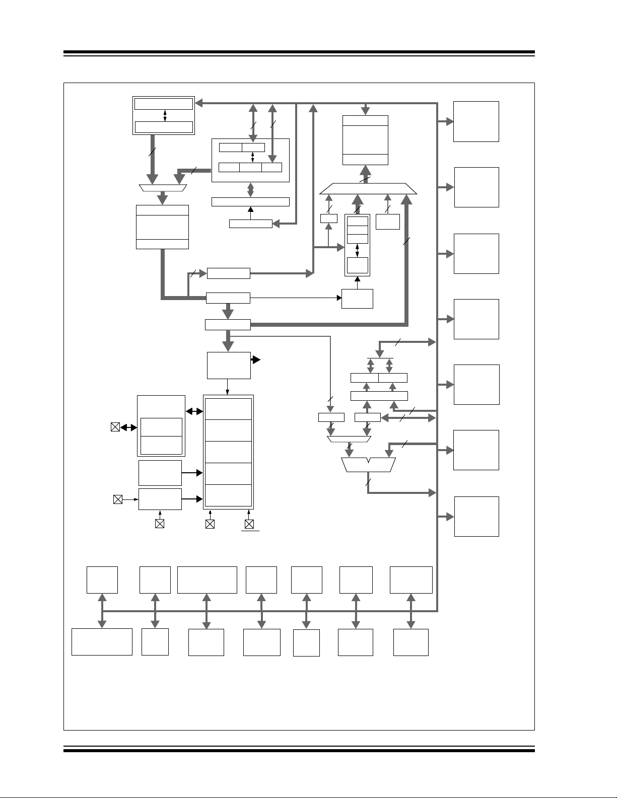
PIC18F87K90 FAMILY
Instruction
Decode and
Control
PORTA
Data Latch
Data Memory
(2/4 Kbytes)
Address Latch
Data Address<12>
12
Access
BSR
FSR0
FSR1
FSR2
inc/dec
logic
Address
4
12
4
PCH PCL
PCLATH
8
31-Level Stack
Program Counter
PRODLPRODH
8 x 8 Multiply
8
BITOP
8
8
ALU<8>
Address Latch
Program Memory
Data Latch
20
8
8
Table Pointer<21>
inc/dec logic
21
8
Data Bus<8>
Table Latch
8
IR
12
3
PCLATU
PCU
Note 1: See Table 1-3 for I/O port pin descriptions.
2: RA6 and RA7 are only available as digital I/O in select oscillator modes. For more information, see Section 3.0 “Oscillator
Configurations”.
3: Unimplemented in the PIC18F65K90.
EUSART1
Comparator
MSSP1/2
3/5/7
(3)
2/4/6/8/10
(3)
/12
(3)
CTMUTimer1
ADC
12-Bit
W
Instruction Bus <16>
STKPTR
Bank
8
State Machine
Control Signals
Decode
8
8
EUSART2
ROM Latch
LCD
PORTC
PORTD
PORTE
PORTF
PORTG
RA0:RA7
(1,2)
RC0:RC7
(1)
RD0:RD7
(1)
RF1:RF7
(1)
RG0:RG5
(1)
PORTB
RB0:RB7
(1)
OSC1/CLKI
OSC2/CLKO
V
DD,
Timing
Generation
V
SS
MCLR
Power-up
Timer
Oscillator
Start-up Timer
Power-on
Reset
Watchdog
Timer
BOR and
LVD
Precision
Reference
Band Gap
INTRC
Oscillator
Regulator
Voltage
VDDCORE/VCAP
ENVREG
Driver
16 MHz
Oscillator
RE0:RE7
(1)
Timer0
4/5/6/7/8/9
(3)
/10
(3)
RTCC
Timer
Timer
1/2/3
CCP
ECCP
1/2/3
FIGURE 1-1: PIC18F6XK90 (64-PIN) BLOCK DIAGRAM
DS39957C-page 12 2011 Microchip Technology Inc.
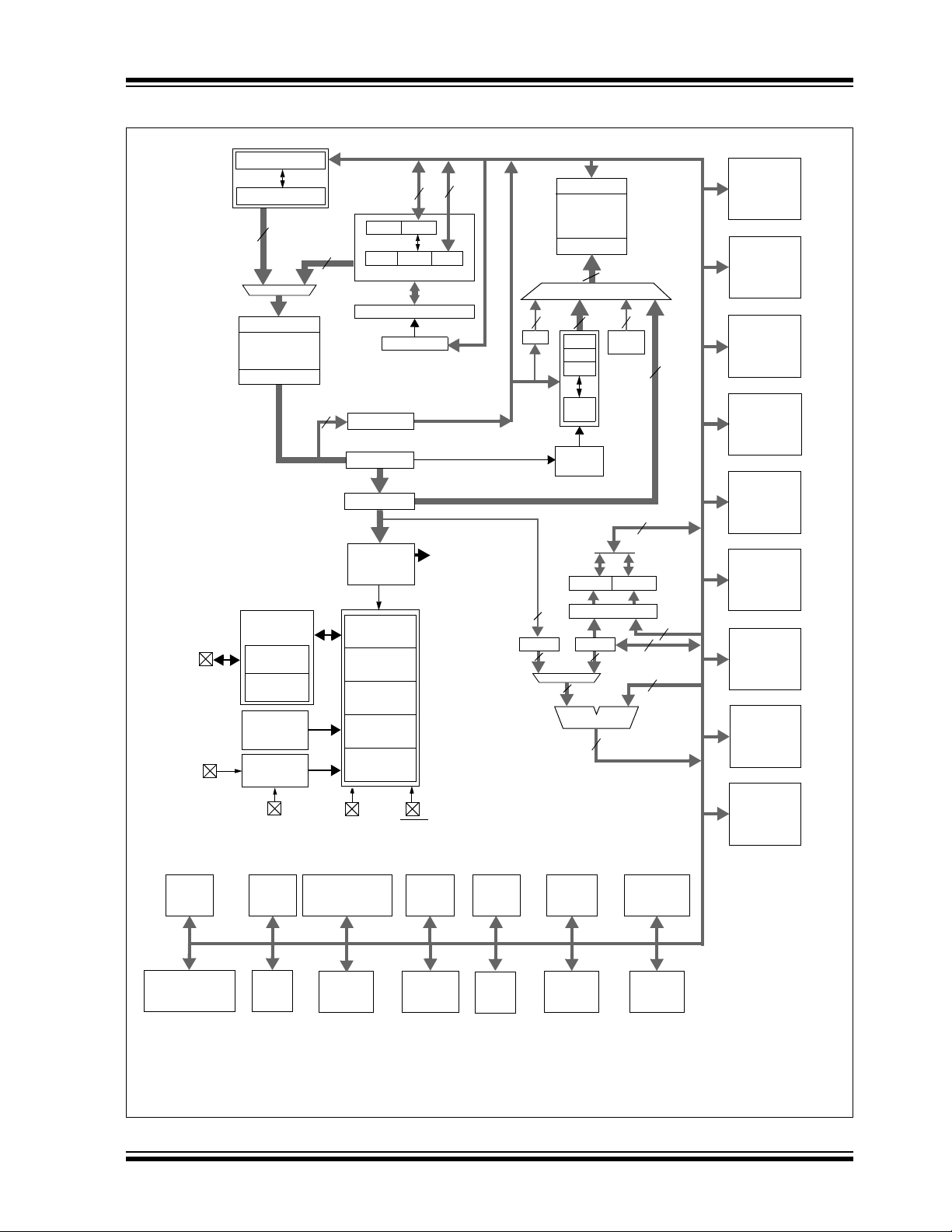
PIC18F87K90 FAMILY
Instruction
Decode and
Control
Data Latch
Address Latch
Data Address<12>
12
Access
BSR
FSR0
FSR1
FSR2
inc/dec
logic
Address
4
12
4
PCH PCL
PCLATH
8
31-Level Stack
Program Counter
PRODLPRODH
8 x 8 Multiply
8
BITOP
8
8
ALU<8>
Address Latch
Program Memory
Data Latch
20
8
8
Table Pointer<21>
inc/dec logic
21
8
Data Bus<8>
Table Latch
8
IR
12
3
PCLATU
PCU
W
Instruction Bus <16>
STKPTR
Bank
8
State Machine
Control Signals
Decode
8
8
ROM Latch
OSC1/CLKI
OSC2/CLKO
V
DD,VSS
MCLR
Power-up
Timer
Oscillator
Start-up Timer
Power-on
Reset
Watchdog
Timer
Precision
Reference
Band Gap
Regulator
Voltage
VDDCORE/VCAP
ENVREG
PORTA
PORTC
PORTD
PORTE
PORTF
PORTG
RA0:RA7
(1,2)
RC0:RC7
(1)
RD0:RD7
(1)
RF1:RF7
(1)
RG0:RG5
(1)
PORTB
RB0:RB7
(1)
PORTH
RH0:RH7
(1)
PORTJ
RJ0:RJ7
(1)
Note 1: See Table 1-3 for I/O port pin descriptions.
2: RA6 and RA7 are only available as digital I/O in select oscillator modes. See Section 3.0 “Oscillator Configurations” for
more information.
3: Unimplemented in the PIC18F85K90.
Timing
Generation
INTRC
Oscillator
16 MHz
Oscillator
RE0:RE7
BOR and
LVD
Data Memory
(2/4 Kbytes)
EUSART1
Comparator
MSSP1/2
3/5/7
(3)
2/4/6/8/10
(3)
/12
(3)
CTMUTimer1
ADC
12-Bit
EUSART2
LCD
Driver
Timer0
4/5/6/7/8/9
(3)
/10
(3)
RTCC
Timer
Timer
1/2/3
CCP
ECCP
1/2/3
FIGURE 1-2: PIC18F8XK90 (80-PIN) BLOCK DIAGRAM
2011 Microchip Technology Inc. DS39957C-page 13

PIC18F87K90 FAMILY
TABLE 1-3: PIC18F6XK90 PINOUT I/O DESCRIPTIONS
Pin Name
Pin Number
QFN/TQFP
Pin
Type
Buffer
Type
Description
/RG5
MCLR
MCLR
RG5
OSC1/CLKI/RA7
OSC1
CLKI
RA7
OSC2/CLKO/RA6
OSC2
CLKO
RA6
Legend: TTL = TTL compatible input CMOS = CMOS compatible input or output
ST = Schmitt Trigger input with CMOS levels Analog = Analog input
I = Input O = Output
P = Power OD = Open-Drain (no P diode to V
2
C™ = I2C/SMBus
I
Note 1: Default assignment for ECCP2 when the CCP2MX Configuration bit is set.
2: Alternate assignment for ECCP2 when the CCP2MX Configuration bit is cleared.
3: Not available on PIC18F65K90 and PIC18F85K90 devices.
7
39
40
I/O
O
O
I/O
I
STSTMaster Clear (input) or programming voltage (input).
This pin is an active-low Reset to the device.
I
I
CMOS
I
CMOS
TTL
—
—
TTL
General purpose, input only pin.
Oscillator crystal or external clock input.
Oscillator crystal input.
External clock source input. Always associated
with pin function, OSC1. (See related OSC1/CLKI,
OSC2/CLKO pins.)
General purpose I/O pin.
Oscillator crystal or clock output.
Oscillator crystal output. Connects to crystal or
resonator in Crystal Oscillator mode.
In certain oscillator modes, OSC2 pin outputs CLKO,
which has 1/4 the frequency of OSC1 and denotes the
instruction cycle rate.
General purpose I/O pin.
DD)
DS39957C-page 14 2011 Microchip Technology Inc.

PIC18F87K90 FAMILY
TABLE 1-3: PIC18F6XK90 PINOUT I/O DESCRIPTIONS (CONTINUED)
Pin Name
RA0/AN0/ULPWU
RA0
AN0
ULPWU
RA1/AN1/SEG18
RA1
AN1
SEG18
RA2/AN2/V
RA2
AN2
V
RA3/AN3/V
RA3
AN3
V
RA4/T0CKI/SEG14
RA4
T0CKI
SEG14
RA5/AN4/SEG15/T1CKI/
T3G/HLVDIN
RA5
AN4
SEG15
T1CKI
T3G
HLVDIN
RA6 See the OSC2/CLKO/RA6 pin.
RA7 See the OSC1/CLKI/RA7 pin.
Legend: TTL = TTL compatible input CMOS = CMOS compatible input or output
Note 1: Default assignment for ECCP2 when the CCP2MX Configuration bit is set.
REF-
REF-
REF+
REF+
ST = Schmitt Trigger input with CMOS levels Analog = Analog input
I = Input O = Output
P = Power OD = Open-Drain (no P diode to V
2
I
C™ = I2C/SMBus
2: Alternate assignment for ECCP2 when the CCP2MX Configuration bit is cleared.
3: Not available on PIC18F65K90 and PIC18F85K90 devices.
Pin Number
QFN/TQFP
24
23
22
21
28
27
Pin
Type
I/O
I
I
I/O
I
O
I/O
I
I
I/O
I
I
I/O
I
O
I/O
I
O
I
I
I
Buffer
Type
TTL
Analog
Analog
TTL
Analog
Analog
TTL
Analog
Analog
TTL
Analog
Analog
ST
ST
Analog
TTL
Analog
Analog
ST
ST
Analog
Description
PORTA is a bidirectional I/O port.
Digital I/O.
Analog Input 0.
Ultra low-power wake-up input.
Digital I/O.
Analog Input 1.
SEG18 output for LCD.
Digital I/O.
Analog Input 2.
A/D reference voltage (low) input.
Digital I/O.
Analog Input 3.
A/D reference voltage (high) input.
Digital I/O.
Timer0 external clock input.
SEG14 output for LCD.
Digital I/O.
Analog Input 4.
SEG15 output for LCD.
Timer1 clock input.
Timer3 external clock gate input.
High/Low-Voltage Detect (HLVD) input.
DD)
2011 Microchip Technology Inc. DS39957C-page 15

PIC18F87K90 FAMILY
TABLE 1-3: PIC18F6XK90 PINOUT I/O DESCRIPTIONS (CONTINUED)
Pin Name
RB0/INT0/SEG30/FLTO
RB0
INT0
SEG30
FLTO
RB1/INT1/SEG8
RB1
INT1
SEG8
RB2/INT2/SEG9/CTED1
RB2
INT2
CTED1
SEG9
RB3/INT3/SEG10/CTED2/
ECCP2/P2A
RB3
INT3
SEG10
CTED2
ECCP2
P2A
RB4/KBI0/SEG11
RB4
KBI0
SEG11
RB5/KBI1/SEG29/T3CKI/
T1G
RB5
KBI1
SEG29
T3CKI
T1G
RB6/KBI2/PGC
RB6
KBI2
PGC
RB7/KBI3/PGD
RB7
KBI3
PGD
Legend: TTL = TTL compatible input CMOS = CMOS compatible input or output
ST = Schmitt Trigger input with CMOS levels Analog = Analog input
I = Input O = Output
P = Power OD = Open-Drain (no P diode to V
2
C™ = I2C/SMBus
I
Note 1: Default assignment for ECCP2 when the CCP2MX Configuration bit is set.
2: Alternate assignment for ECCP2 when the CCP2MX Configuration bit is cleared.
3: Not available on PIC18F65K90 and PIC18F85K90 devices.
Pin Number
QFN/TQFP
48
47
46
45
44
43
42
37
Pin
Type
I/O
I
O
I
I/O
I
O
I/O
I
I
O
I/O
I
O
I
I/O
O
I/O
I
O
I/O
I
O
I
I
I/O
I
I/O
I/O
I
I/O
Buffer
Type
TTL
ST
Analog
ST
TTL
ST
Analog
TTL
ST
ST
Analog
TTL
ST
Analog
ST
ST
—
TTL
TTL
Analog
TTL
TTL
Analog
ST
ST
TTL
TTL
ST
TTL
TTL
ST
Description
PORTB is a bidirectional I/O port. PORTB can be software
programmed for internal weak pull-ups on all inputs.
Digital I/O.
External Interrupt 0.
SEG30 output for LCD.
Enhanced PWM Fault input for ECCP1/2/3.
Digital I/O.
External Interrupt 1.
SEG8 output for LCD.
Digital I/O.
External Interrupt 2.
CTMU Edge 1 input.
SEG9 output for LCD.
Digital I/O.
External Interrupt 3.
SEG10 output for LCD.
CTMU Edge 2 input.
Capture 2 input/Compare 2 output/PWM2.
Enhanced PWM2 Output A.
Digital I/O.
Interrupt-on-change pin.
SEG11 output for LCD.
Digital I/O.
Interrupt-on-change pin.
SEG29 output for LCD.
Timer3 clock input.
Timer1 external clock gate input.
Digital I/O.
Interrupt-on-change pin.
In-Circuit Debugger and ICSP™ programming clock pin.
Digital I/O.
Interrupt-on-change pin.
In-Circuit Debugger and ICSP programming data pin.
DD)
DS39957C-page 16 2011 Microchip Technology Inc.

PIC18F87K90 FAMILY
TABLE 1-3: PIC18F6XK90 PINOUT I/O DESCRIPTIONS (CONTINUED)
Pin Name
RC0/SOSCO/SCLKI
RC0
SOSCO
SCLKI
RC1/SOSCI/ECCP2/P2A/
SEG32
RC1
SOSCI
ECCP2
P2A
SEG32
RC2/ECCP1/P1A/SEG13
RC2
ECCP1
P1A
SEG13
RC3/SCK1/SCL1/SEG17
RC3
SCK1
SCL1
SEG17
RC4/SDI1/SDA1/SEG16
RC4
SDI1
SDA1
SEG16
RC5/SDO1/SEG12
RC5
SDO1
SEG12
RC6/TX1/CK1/SEG27
RC6
TX1
CK1
SEG27
RC7/RX1/DT1/SEG28
RC7
RX1
DT1
SEG28
Legend: TTL = TTL compatible input CMOS = CMOS compatible input or output
Note 1: Default assignment for ECCP2 when the CCP2MX Configuration bit is set.
(1)
ST = Schmitt Trigger input with CMOS levels Analog = Analog input
I = Input O = Output
P = Power OD = Open-Drain (no P diode to V
2
C™ = I2C/SMBus
I
2: Alternate assignment for ECCP2 when the CCP2MX Configuration bit is cleared.
3: Not available on PIC18F65K90 and PIC18F85K90 devices.
Pin Number
QFN/TQFP
30
29
33
34
35
36
31
32
Pin
Type
I/O
O
I
I/O
I
I/O
O
O
I/O
I/O
O
O
I/O
I/O
I/O
O
I/O
I
I/O
O
I/O
O
O
I/O
O
I/O
O
I/O
I
I/O
O
Buffer
Type
ST
—
ST
ST
CMOS
ST
—
Analog
ST
ST
—
Analog
ST
ST
2
C
I
Analog
ST
ST
2
C
I
Analog
ST
—
Analog
ST
—
ST
Analog
ST
ST
ST
Analog
Description
PORTC is a bidirectional I/O port.
Digital I/O.
SOSC oscillator output.
Digital SOSC input.
Digital I/O.
SOSC oscillator input.
Capture 2 input/Compare 2 output/PWM2 output.
Enhanced PWM2 Output A.
SEG32 output for LCD.
Digital I/O.
Capture 1 input/Compare 1 output/PWM1 output.
Enhanced PWM1 Output A.
SEG13 output for LCD.
Digital I/O.
Synchronous serial clock input/output for SPI mode.
Synchronous serial clock input/output for I2C™ mode.
SEG17 output for LCD.
Digital I/O.
SPI data in.
I2C data I/O.
SEG16 output for LCD.
Digital I/O.
SPI data out.
SEG12 output for LCD.
Digital I/O.
EUSART asynchronous transmit.
EUSART synchronous clock (see related RX1/DT1).
SEG27 output for LCD.
Digital I/O.
EUSART asynchronous receive.
EUSART synchronous data (see related TX1/CK1).
SEG28 output for LCD.
DD)
2011 Microchip Technology Inc. DS39957C-page 17

PIC18F87K90 FAMILY
TABLE 1-3: PIC18F6XK90 PINOUT I/O DESCRIPTIONS (CONTINUED)
Pin Name
RD0/SEG0/CTPLS
RD0
SEG0
CTPLS
RD1/SEG1/T5CKI/T7G
RD1
SEG1
T5CKI
T7G
RD2/SEG2
RD2
SEG2
RD3/SEG3
RD3
SEG3
RD4/SEG4/SDO2
RD4
SEG4
SDO2
RD5/SEG5/SDI2/SDA2
RD5
SEG5
SDI2
SDA2
RD6/SEG6/SCK2/SCL2
RD6
SEG6
SCK2
SCL2
RD7/SEG7/SS2
RD7
SEG7
SS2
Legend: TTL = TTL compatible input CMOS = CMOS compatible input or output
Note 1: Default assignment for ECCP2 when the CCP2MX Configuration bit is set.
2: Alternate assignment for ECCP2 when the CCP2MX Configuration bit is cleared.
3: Not available on PIC18F65K90 and PIC18F85K90 devices.
ST = Schmitt Trigger input with CMOS levels Analog = Analog input
I = Input O = Output
P = Power OD = Open-Drain (no P diode to V
2
I
C™ = I2C/SMBus
Pin Number
QFN/TQFP
58
55
54
53
52
51
50
49
Pin
Buffer
Type
Type
I/O
O
Analog
O
I/O
O
Analog
I
I
I/OOST
Analog
I/OOST
Analog
I/O
O
Analog
O
I/O
O
Analog
I
I/O
I/O
O
Analog
I/O
I/O
I/O
O
Analog
I
PORTD is a bidirectional I/O port.
ST
—
ST
ST
ST
ST
—
ST
ST
2
I
ST
ST
2
I
C
ST
TTL
C
Digital I/O.
SEG0 output for LCD.
CTMU pulse generator output.
Digital I/O.
SEG1 output for LCD.
Timer5 clock input.
Timer7 external clock gate input.
Digital I/O.
SEG2 output for LCD.
Digital I/O.
SEG3 output for LCD.
Digital I/O.
SEG4 output for LCD.
SPI data out.
Digital I/O.
SEG5 output for LCD.
SPI data in.
2
C™ data I/O.
I
Digital I/O.
SEG6 output for LCD.
Synchronous serial clock.
Synchronous serial clock for I2C mode.
Digital I/O.
SEG7 output for LCD.
SPI slave select input.
Description
DD)
DS39957C-page 18 2011 Microchip Technology Inc.

PIC18F87K90 FAMILY
TABLE 1-3: PIC18F6XK90 PINOUT I/O DESCRIPTIONS (CONTINUED)
Pin Name
RE0/LCDBIAS1/P2D
RE0
LCDBIAS1
P2D
RE1/LCDBIAS2/P2C
RE1
LCDBIAS2
P2C
RE2/LCDBIAS3/P2B/
CCP10
RE2
LCDBIAS3
P2B
(3)
CCP10
RE3/COM0/P3C/CCP9/
REFO
RE3
COM0
P3C
CCP9
REFO
RE4/COM1/P3B/CCP8
RE4
COM1
P3B
CCP8
RE5/COM2/P1C/CCP7
RE5
COM2
P1C
CCP7
RE6/COM3/P1B/CCP6
RE6
COM3
P1B
CCP6
RE7/ECCP2/SEG31/P2A
RE7
ECCP2
SEG31
P2A
Legend: TTL = TTL compatible input CMOS = CMOS compatible input or output
Note 1: Default assignment for ECCP2 when the CCP2MX Configuration bit is set.
(3)
(2)
ST = Schmitt Trigger input with CMOS levels Analog = Analog input
I = Input O = Output
P = Power OD = Open-Drain (no P diode to V
2
C™ = I2C/SMBus
I
2: Alternate assignment for ECCP2 when the CCP2MX Configuration bit is cleared.
3: Not available on PIC18F65K90 and PIC18F85K90 devices.
Pin Number
QFN/TQFP
2
1
64
63
62
61
60
59
Pin
Type
I/O
I
O
I/O
I
O
I/O
I
O
I/O
I/O
O
O
I/O
O
I/O
O
O
I/O
I/O
O
O
I/O
I/O
O
O
I/O
I/O
I/O
O
O
Buffer
Type
ST
Analog
—
ST
Analog
—
ST
Analog
—
S/T
ST
Analog
—
S/T
—
ST
Analog
—
S/T
ST
Analog
—
S/T
ST
Analog
—
S/T
ST
ST
Analog
—
Description
PORTE is a bidirectional I/O port.
Digital I/O.
BIAS1 input for LCD.
EECP2 PWM Output D.
Digital I/O.
BIAS2 input for LCD.
ECCP2 PWM Output C.
Digital I/O.
BIAS3 input for LCD.
ECCP2 PWM Output B.
Capture 10 input/Compare 10 output/PWM10 output.
Digital I/O.
COM0 output for LCD.
ECCP3 PWM Output C.
Capture 9 input/Compare 9 output/PWM9 output.
Reference clock out.
Digital I/O.
COM1 output for LCD.
ECCP3 PWM Output B.
Capture 8 input/Compare 8 output/PWM8 output.
Digital I/O.
COM2 output for LCD.
ECCP1 PWM Output C.
Capture 7 input/Compare 7 output/PWM7 output.
Digital I/O.
COM3 output for LCD.
ECCP1 PWM Output B.
Capture 6 input/Compare 6 output/PWM6 output.
Digital I/O.
Capture 2 input/Compare 2 output/PWM2 output.
SEG31 Output for LCD.
ECCP2 PWM output A.
DD)
2011 Microchip Technology Inc. DS39957C-page 19

PIC18F87K90 FAMILY
TABLE 1-3: PIC18F6XK90 PINOUT I/O DESCRIPTIONS (CONTINUED)
Pin Name
RF1/AN6/C2OUT/SEG19/
CTDIN
RF1
AN6
C2OUT
SEG19
CTDIN
RF2/AN7/C1OUT/SEG20
RF2
AN7
C1OUT
SEG20
RF3/AN8/SEG21/C2INB/
CTMUI
RF3
AN8
SEG21
C2INB
CTMUI
RF4/AN9/SEG22/C2INA
RF4
AN9
SEG22
C2INA
RF5/AN10/CV
SEG23/C1INB
RF5
AN10
REF
CV
SEG23
C1INB
RF6/AN11/SEG24/C1INA
RF6
AN11
SEG24
C1INA
RF7/AN5/SS1
RF7
AN5
SS1
SEG25
Legend: TTL = TTL compatible input CMOS = CMOS compatible input or output
Note 1: Default assignment for ECCP2 when the CCP2MX Configuration bit is set.
2: Alternate assignment for ECCP2 when the CCP2MX Configuration bit is cleared.
3: Not available on PIC18F65K90 and PIC18F85K90 devices.
REF/
/SEG25
ST = Schmitt Trigger input with CMOS levels Analog = Analog input
I = Input O = Output
P = Power OD = Open-Drain (no P diode to V
2
C™ = I2C/SMBus
I
Pin Number
QFN/TQFP
17
16
15
14
13
12
11
Pin
Type
I/O
I
O
O
I
I/O
I
O
O
I/O
I
O
I
O
I/O
I
O
I
I/O
I
O
O
I
I/O
I
O
I
I/O
O
I
O
Buffer
Type
ST
Analog
—
Analog
ST
ST
Analog
—
Analog
ST
Analog
Analog
Analog
—
ST
Analog
Analog
Analog
ST
Analog
Analog
Analog
Analog
ST
Analog
Analog
Analog
ST
AnalogT
TL
Analog
Description
PORTF is a bidirectional I/O port.
Digital I/O.
Analog Input 6.
Comparator 2 output.
SEG19 output for LCD.
CTMU pulse delay input.
Digital I/O.
Analog Input 7.
Comparator 1 output.
SEG20 output for LCD.
Digital I/O.
Analog Input 8.
SEG21 output for LCD.
Comparator 2 Input B.
CTMU pulse generator charger for the C2INB
comparator input.
Digital I/O.
Analog Input 9.
SEG22 output for LCD
Comparator 2 Input A.
Digital I/O.
Analog Input 10.
Comparator reference voltage output.
SEG23 output for LCD.
Comparator 1 Input B.
Digital I/O.
Analog Input 11.
SEG24 output for LCD
Comparator 1 Input A.
Digital I/O.
Analog Input 5.
SPI1 slave select input.
SEG25 output for LCD.
DD)
DS39957C-page 20 2011 Microchip Technology Inc.

PIC18F87K90 FAMILY
TABLE 1-3: PIC18F6XK90 PINOUT I/O DESCRIPTIONS (CONTINUED)
Pin Name
RG0/ECCP3/P3A
RG0
ECCP3
P3A
RG1/TX2/CK2/AN19/
C3OUT
RG1
TX2
CK2
AN19
C3OUT
RG2/RX2/DT2/AN18/
C3INA
RG2
RX2
DT2
AN18
C3INA
RG3/CCP4/AN17/P3D/
C3INB
RG3
CCP4
AN17
P3D
C3INB
RG4/SEG26/RTCC/
T7CKI/T5G/CCP5/AN16/
P1D/C3INC
RG4
SEG26
RTCC
(3)
T7CKI
T5G
CCP5
AN16
P1D
C3INC
RG5 7 See the MCLR
Legend: TTL = TTL compatible input CMOS = CMOS compatible input or output
Note 1: Default assignment for ECCP2 when the CCP2MX Configuration bit is set.
ST = Schmitt Trigger input with CMOS levels Analog = Analog input
I = Input O = Output
P = Power OD = Open-Drain (no P diode to V
2
C™ = I2C/SMBus
I
2: Alternate assignment for ECCP2 when the CCP2MX Configuration bit is cleared.
3: Not available on PIC18F65K90 and PIC18F85K90 devices.
Pin Number
QFN/TQFP
3
4
5
6
8
Pin
Type
I/O
I/O
O
I/O
O
I/O
I
O
I/O
I
I/O
I
I
I/O
I/O
I
O
I
I/O
O
O
I
I
I/O
I
O
I
Buffer
Type
ST
ST
—
ST
—
ST
Analog
—
ST
ST
ST
Analog
Analog
ST
S/T
Analog
—
Analog
ST
Analog
—
ST
ST
ST
Analog
—
Analog
Description
PORTG is a bidirectional I/O port.
Digital I/O.
Capture 3 input/Compare 3 output/PWM3 output.
ECCP3 PWM Output A.
Digital I/O.
USART asynchronous transmit.
USART synchronous clock (see related RX2/DT2).
Analog Input 19.
Comparator 3 output.
Digital I/O.
EUSART asynchronous receive.
EUSART synchronous data (see related TX2/CK2).
Analog Input 18.
Comparator 3 Input A.
Digital I/O.
Capture 4 input/Compare 4 output/PWM4 output.
Analog Input 18.
ECCP3 PWM Output D.
Comparator 3 Input B.
Digital I/O.
SEG26 output for LCD.
RTCC output
Timer7 clock input.
Timer5 external clock gate input.
Capture 5 input/Compare 5 output/PWM5 output.
Analog Input 16.
ECCP1 PWM Output D.
Comparator 3 Input C.
/RG5 pin.
DD)
2011 Microchip Technology Inc. DS39957C-page 21

PIC18F87K90 FAMILY
TABLE 1-3: PIC18F6XK90 PINOUT I/O DESCRIPTIONS (CONTINUED)
Pin Name
VSS 9, 25, 41, 56 P — Ground reference for logic and I/O pins.
V
DD 26, 38, 57 P — Positive supply for logic and I/O pins.
AVSS 20 P — Ground reference for analog modules.
AVDD 19 P — Positive supply for analog modules.
ENVREG 18 I ST Enable for on-chip voltage regulator.
VDDCORE/VCAP
VDDCORE
VCAP
Legend: TTL = TTL compatible input CMOS = CMOS compatible input or output
ST = Schmitt Trigger input with CMOS levels Analog = Analog input
I = Input O = Output
P = Power OD = Open-Drain (no P diode to V
2
C™ = I2C/SMBus
I
Note 1: Default assignment for ECCP2 when the CCP2MX Configuration bit is set.
2: Alternate assignment for ECCP2 when the CCP2MX Configuration bit is cleared.
3: Not available on PIC18F65K90 and PIC18F85K90 devices.
Pin Number
QFN/TQFP
10
Pin
Buffer
Type
Type
P—
Description
Core logic power or external filter capacitor connection.
External filter capacitor connection (regulator
enabled/disabled).
DD)
TABLE 1-4: PIC18F8XK90 PINOUT I/O DESCRIPTIONS
Pin Name
/RG5
MCLR
RG5
OSC1/CLKI/RA7
OSC1
CLKI
RA7
OSC2/CLKO/RA6
OSC2
CLKO
RA6
Legend: TTL = TTL compatible input CMOS = CMOS compatible input or output
ST = Schmitt Trigger input with CMOS levels Analog = Analog input
I = Input O = Output
P = Power OD = Open-Drain (no P diode to V
2
C™ = I2C/SMBus
I
Note 1: Default assignment for ECCP2 when the CCP2MX Configuration bit is set.
2: Alternate assignment for ECCP2 when the CCP2MX Configuration bit is cleared.
3: Not available on PIC18F65K90 and PIC18F85K90 devices.
4: The CCP6, CCP7, CCP8 and CCP9 pin placement depends on the ECCPMX Configuration bit setting.
Pin Number
TQFP
9
49
50
Pin
Type
I
I
I
I
I/O
O
O
I/O
Buffer
Type
STSTMaster Clear (input) or programming voltage (input).
This pin is an active-low Reset to the device.
General purpose, input only pin.
Oscillator crystal or external clock input.
CMOS
CMOS
TTL
—
—
TTL
Oscillator crystal input.
External clock source input. Always associated
with pin function, OSC1. (See related OSC1/CLKI,
OSC2/CLKO pins.)
General purpose I/O pin.
Oscillator crystal or clock output.
Oscillator crystal output. Connects to crystal or
resonator in Crystal Oscillator mode.
In certain oscillator modes, OSC2 pin outputs CLKO,
which has 1/4 the frequency of OSC1 and denotes the
instruction cycle rate.
General purpose I/O pin.
Description
DD)
DS39957C-page 22 2011 Microchip Technology Inc.

PIC18F87K90 FAMILY
TABLE 1-4: PIC18F8XK90 PINOUT I/O DESCRIPTIONS (CONTINUED)
Pin Name
RA0/AN0/ULPWU
RA0
AN0
ULPWU
RA1/AN1/SEG18
RA1
AN1
SEG18
RA2/AN2/V
RA2
AN2
V
RA3/AN3/V
RA3
AN3
V
RA4/T0CKI/SEG14
RA4
T0CKI
SEG14
RA5/AN4/SEG15/T1CKI/
T3G/HLVDIN
RA5
AN4
SEG15
T1CKI
T3G
HLVDIN
RA6 See the OSC2/CLKO/RA6 pin.
RA7 See the OSC1/CLKI/RA7 pin.
Legend: TTL = TTL compatible input CMOS = CMOS compatible input or output
Note 1: Default assignment for ECCP2 when the CCP2MX Configuration bit is set.
REF-
REF-
REF+
REF+
ST = Schmitt Trigger input with CMOS levels Analog = Analog input
I = Input O = Output
P = Power OD = Open-Drain (no P diode to V
2
I
C™ = I2C/SMBus
2: Alternate assignment for ECCP2 when the CCP2MX Configuration bit is cleared.
3: Not available on PIC18F65K90 and PIC18F85K90 devices.
4: The CCP6, CCP7, CCP8 and CCP9 pin placement depends on the ECCPMX Configuration bit setting.
Pin Number
TQFP
30
29
28
27
34
33
Pin
Type
I/O
I
I
I/O
I
O
I/O
I
I
I/O
I
I
I/O
I
O
I/O
I
O
I
I
I
Buffer
Type
TTL
Analog
Analog
TTL
Analog
Analog
TTL
Analog
Analog
TTL
Analog
Analog
ST
ST
Analog
TTL
Analog
Analog
ST
ST
Analog
Description
PORTA is a bidirectional I/O port.
Digital I/O.
Analog Input 0.
Ultra low-power wake-up input.
Digital I/O.
Analog Input 1.
SEG18 output for LCD.
Digital I/O.
Analog Input 2.
A/D reference voltage (low) input.
Digital I/O.
Analog Input 3.
A/D reference voltage (high) input.
Digital I/O.
Timer0 external clock input.
SEG14 output for LCD.
Digital I/O.
Analog Input 4.
SEG15 output for LCD.
Timer1 clock input.
Timer3 external clock gate input.
High/Low-Voltage Detect (HLVD) input.
DD)
2011 Microchip Technology Inc. DS39957C-page 23

PIC18F87K90 FAMILY
TABLE 1-4: PIC18F8XK90 PINOUT I/O DESCRIPTIONS (CONTINUED)
Pin Name
RB0/INT0/SEG30/FLT0
RB0
INT0
SEG30
FLT0
RB1/INT1/SEG8
RB1
INT1
SEG8
RB2/INT2/SEG9/CTED1
RB2
INT2
SEG9
CTED1
RB3/INT3/SEG10/
CTED2/ECCP2/P2A
RB3
INT3
SEG10
CTED2
ECCP2
P2A
RB4/KBI0/SEG11
RB4
KBI0
SEG11
RB5/KBI1/SEG29/T3CKI/
T1G
RB5
KBI1
SEG29
T3CKI
T1G
Legend: TTL = TTL compatible input CMOS = CMOS compatible input or output
ST = Schmitt Trigger input with CMOS levels Analog = Analog input
I = Input O = Output
P = Power OD = Open-Drain (no P diode to V
2
C™ = I2C/SMBus
I
Note 1: Default assignment for ECCP2 when the CCP2MX Configuration bit is set.
2: Alternate assignment for ECCP2 when the CCP2MX Configuration bit is cleared.
3: Not available on PIC18F65K90 and PIC18F85K90 devices.
4: The CCP6, CCP7, CCP8 and CCP9 pin placement depends on the ECCPMX Configuration bit setting.
Pin Number
TQFP
58
57
56
55
54
53
Pin
Type
I/O
I
O
I
I/O
I
O
I/O
I
O
I
I/O
I
O
I
I/O
O
I/O
I
O
I/O
I
O
I
I
Buffer
Type
TTL
ST
Analog
ST
TTL
ST
Analog
TTL
ST
Analog
ST
TTL
ST
Analog
ST
ST
ST
TTL
TTL
Analog
TTL
TTL
Analog
ST
ST
Description
PORTB is a bidirectional I/O port. PORTB can be software
programmed for internal weak pull-ups on all inputs.
Digital I/O.
External Interrupt 0.
SEG30 output for LCD.
Enhanced PWM Fault input for ECCP1/2/3.
Digital I/O.
External Interrupt 1.
SEG8 output for LCD.
Digital I/O.
External Interrupt 2.
SEG9 output for LCD.
CTMU Edge 1 input.
Digital I/O.
External Interrupt 3.
SEG10 output for LCD.
CTMU Edge 2 input.
Capture 2 input/Compare 2 output/PWM2 output.
Enhanced PWM 2 Output A.
Digital I/O.
Interrupt-on-change pin.
SEG11 output for LCD.
Digital I/O.
Interrupt-on-change pin.
SEG29 output for LCD.
Timer3 clock input.
Timer1 external clock gate input.
DD)
DS39957C-page 24 2011 Microchip Technology Inc.

PIC18F87K90 FAMILY
TABLE 1-4: PIC18F8XK90 PINOUT I/O DESCRIPTIONS (CONTINUED)
Pin Name
RB6/KBI2/PGC
RB6
KBI2
PGC
RB7/KBI3/PGD
RB7
KBI3
PGD
Legend: TTL = TTL compatible input CMOS = CMOS compatible input or output
ST = Schmitt Trigger input with CMOS levels Analog = Analog input
I = Input O = Output
P = Power OD = Open-Drain (no P diode to V
2
I
C™ = I2C/SMBus
Note 1: Default assignment for ECCP2 when the CCP2MX Configuration bit is set.
2: Alternate assignment for ECCP2 when the CCP2MX Configuration bit is cleared.
3: Not available on PIC18F65K90 and PIC18F85K90 devices.
4: The CCP6, CCP7, CCP8 and CCP9 pin placement depends on the ECCPMX Configuration bit setting.
Pin Number
TQFP
52
47
Pin
Type
I/O
I
I/O
I/O
I
I/O
Buffer
Type
TTL
TTL
ST
TTL
TTL
ST
Description
Digital I/O.
Interrupt-on-change pin.
In-Circuit Debugger and ICSP™ programming clock pin.
Digital I/O.
Interrupt-on-change pin.
In-Circuit Debugger and ICSP programming data pin.
DD)
2011 Microchip Technology Inc. DS39957C-page 25

PIC18F87K90 FAMILY
TABLE 1-4: PIC18F8XK90 PINOUT I/O DESCRIPTIONS (CONTINUED)
Pin Name
RC0/SOSCO/SCKLI
RC0
SOSCO
SCKLI
RC1/SOSCI/ECCP2/
SEG32/P2A
RC1
SOSCI
(1)
ECCP2
SEG32
P2A
RC2/ECCP1/P1A/SEG13
RC2
ECCP1
P1A
SEG13
RC3/SCK1/SCL1/SEG17
RC3
SCK1
SCL1
SEG17
RC4/SDI1/SDA1/SEG16
RC4
SDI1
SDA1
SEG16
RC5/SDO1/SEG12
RC5
SDO1
SEG12
RC6/TX1/CK1/SEG27
RC6
TX1
CK1
SEG27
RC7/RX1/DT1/SEG28
RC7
RX1
DT1
SEG28
Legend: TTL = TTL compatible input CMOS = CMOS compatible input or output
ST = Schmitt Trigger input with CMOS levels Analog = Analog input
I = Input O = Output
P = Power OD = Open-Drain (no P diode to V
2
C™ = I2C/SMBus
I
Note 1: Default assignment for ECCP2 when the CCP2MX Configuration bit is set.
2: Alternate assignment for ECCP2 when the CCP2MX Configuration bit is cleared.
3: Not available on PIC18F65K90 and PIC18F85K90 devices.
4: The CCP6, CCP7, CCP8 and CCP9 pin placement depends on the ECCPMX Configuration bit setting.
Pin Number
TQFP
36
35
43
44
45
46
37
38
Pin
Type
I/O
O
I
I/O
I
I/O
O
O
I/O
I/O
O
O
I/O
I/O
I/O
O
I/O
I
I/O
O
I/O
O
O
I/O
O
I/O
O
I/O
I
I/O
O
Buffer
Type
ST
—
ST
ST
CMOS
ST
Analog
—
ST
ST
—
Analog
ST
ST
ST
Analog
ST
ST
ST
Analog
ST
—
Analog
ST
—
ST
Analog
ST
ST
ST
Analog
Description
PORTC is a bidirectional I/O port.
Digital I/O.
SOSC oscillator output.
Digital SOSC input.
Digital I/O.
SOSC oscillator input.
Capture 2 input/Compare 2 output/PWM2 output.
SEG32 output for LCD.
Enhanced PWM 2 Output A.
Digital I/O.
Capture 1 input/Compare 1 output/PWM1 output.
Enhanced PWM 1 Output A.
SEG13 output for LCD.
Digital I/O.
Synchronous serial clock input/output for SPI mode.
Synchronous serial clock input/output for I
SEG17 output for LCD.
Digital I/O.
SPI data in.
2
C data I/O.
I
SEG16 output for LCD.
Digital I/O.
SPI data out.
SEG12 output for LCD.
Digital I/O.
EUSART asynchronous transmit.
EUSART synchronous clock (see related RX1/DT1).
SEG27 output for LCD.
Digital I/O.
EUSART asynchronous receive.
EUSART synchronous data (see related TX1/CK1).
SEG28 output for LCD.
2
C™ mode.
DD)
DS39957C-page 26 2011 Microchip Technology Inc.

PIC18F87K90 FAMILY
TABLE 1-4: PIC18F8XK90 PINOUT I/O DESCRIPTIONS (CONTINUED)
Pin Name
RD0/SEG0/CTPLS
RD0
SEG0
CTPLS
RD1/SEG1/T5CKI/T7G
RD1
SEG1
T5CKI
T7G
RD2/SEG2
RD2
SEG2
RD3/SEG3
RD3
SEG3
RD4/SEG4/SDO2
RD4
SEG4
SDO2
RD5/SEG5/SDI2/SDA2
RD5
SEG5
SDI2
SDA2
RD6/SEG6/SCK2/SCL2
RD6
SEG6
SCK2
SCL2
RD7/SEG7/SS2
RD7
SEG7
SS2
Legend: TTL = TTL compatible input CMOS = CMOS compatible input or output
Note 1: Default assignment for ECCP2 when the CCP2MX Configuration bit is set.
2: Alternate assignment for ECCP2 when the CCP2MX Configuration bit is cleared.
3: Not available on PIC18F65K90 and PIC18F85K90 devices.
4: The CCP6, CCP7, CCP8 and CCP9 pin placement depends on the ECCPMX Configuration bit setting.
ST = Schmitt Trigger input with CMOS levels Analog = Analog input
I = Input O = Output
P = Power OD = Open-Drain (no P diode to V
2
I
C™ = I2C/SMBus
Pin Number
TQFP
72
69
68
67
66
65
64
63
Pin
Buffer
Type
Type
I/O
O
Analog
O
I/O
O
Analog
I
I
I/OOST
Analog
I/OOST
Analog
I/O
O
Analog
O
I/O
O
Analog
I
I/O
I/O
O
Analog
I/O
I/O
I/O
O
Analog
I
PORTD is a bidirectional I/O port.
ST
ST
ST
ST
ST
ST
—
ST
ST
2
C
I
ST
ST
2
I
C
ST
TTL
Digital I/O.
SEG0 output for LCD.
CTMU pulse generator output.
Digital I/O.
SEG1 output for LCD.
Timer5 clock input.
Timer7 external clock gate input.
Digital I/O.
SEG2 output for LCD.
Digital I/O.
SEG3 output for LCD.
Digital I/O.
SEG4 output for LCD.
SPI data out.
Digital I/O.
SEG5 output for LCD.
SPI data in.
2
C™ data in.
I
Digital I/O.
SEG6 output for LCD.
Synchronous serial clock input/output for SPI mode.
Synchronous serial clock input/output for I2C™ mode.
Digital I/O.
SEG7 output for LCD.
SPI slave select input.
Description
DD)
2011 Microchip Technology Inc. DS39957C-page 27

PIC18F87K90 FAMILY
TABLE 1-4: PIC18F8XK90 PINOUT I/O DESCRIPTIONS (CONTINUED)
Pin Name
Pin Number
TQFP
RE0/LCDBIAS1/P2D
4
RE0
LCDBIAS1
P2D
RE1/LCDBIAS2/P2C
3
RE1
LCDBIAS2
P2C
RE2/LCDBIAS3/P2B/
78
CCP10
RE2
LCDBIAS3
P2B
(3)
CCP10
RE3/COM0/P3C/CCP9/
77
REFO
RE3
COM0
P3C
(3)(4)
CCP9
REFO
RE4/COM1/P3B/CCP8
76
RE4
COM1
P3B
(4)
CCP8
RE5/COM2/P1C/CCP7
75
RE5
COM2
P1C
(4)
CCP7
RE6/COM3/P1B/CCP6
74
RE6
COM3
P1B
(4)
CCP6
RE7/ECCP2/P2A/SEG31
RE7
(2)
ECCP2
73
P2A
SEG31
Legend: TTL = TTL compatible input CMOS = CMOS compatible input or output
ST = Schmitt Trigger input with CMOS levels Analog = Analog input
I = Input O = Output
P = Power OD = Open-Drain (no P diode to V
2
C™ = I2C/SMBus
I
Note 1: Default assignment for ECCP2 when the CCP2MX Configuration bit is set.
2: Alternate assignment for ECCP2 when the CCP2MX Configuration bit is cleared.
3: Not available on PIC18F65K90 and PIC18F85K90 devices.
4: The CCP6, CCP7, CCP8 and CCP9 pin placement depends on the ECCPMX Configuration bit setting.
Pin
Type
I/O
I
O
I/O
I
O
I/O
I
O
I/O
I/O
O
O
I/O
O
I/O
O
O
I/O
I/O
O
O
I/O
I/O
O
O
I/O
I/O
I/O
O
O
Buffer
Type
ST
Analog
—
ST
Analog
—
ST
Analog
ST
ST
ST
Analog
—
S/T
—
ST
Analog
—
ST
ST
Analog
—
ST
ST
Analog
—
ST
ST
ST
—
Analog
Description
PORTE is a bidirectional I/O port.
Digital I/O.
BIAS1 input for LCD.
ECCP2 PWM Output D.
Digital I/O.
BIAS2 input for LCD.
ECCP2 PWM Output C.
Digital I/O.
BIAS3 input for LCD.
ECCP2 PWM Output B.
Capture 10 input/Compare 10 output/PWM10 output.
Digital I/O.
COM0 output for LCD.
ECCP3 PWM Output C.
Capture 9 input/Compare 9 output/PWM9 output.
Reference clock out.
Digital I/O.
COM1 output for LCD.
ECCP4 PWM Output B.
Capture 8 input/Compare 8 output/PWM8 output.
Digital I/O.
COM2 output for LCD.
ECCP1 PWM Output C.
Capture 7 input/Compare 7 output/PWM7 output.
Digital I/O.
COM3 output for LCD.
ECCP1 PWM Output B.
Capture 6 input/Compare 6 output/PWM6 output.
Digital I/O.
Capture 2 input/Compare 2 output/PWM2 output.
ECCP2 PWM Output A.
SEG31 output for LCD.
DD)
DS39957C-page 28 2011 Microchip Technology Inc.

PIC18F87K90 FAMILY
TABLE 1-4: PIC18F8XK90 PINOUT I/O DESCRIPTIONS (CONTINUED)
Pin Name
RF1/AN6/C2OUT/SEG19/
CTDIN
RF1
AN6
C2OUT
SEG19
CTDIN
RF2/AN7/C1OUT/
SEG20/CTMUI
RF2
AN7
C1OUT
SEG20
CTMUI
RF3/AN8/SEG21/C2INB
RF3
AN8
SEG21
C2INB
RF4/AN9/SEG22/C2INA
RF4
AN9
SEG22
C2INA
RF5/AN10/CV
SEG23/C1INB
RF5
AN10
CVREF
SEG23
C1INB
RF6/AN11/SEG24/C1INA
RF6
AN11
SEG24
C1INA
RF7/AN5/SS1
RF7
AN5
SS1
SEG25
Legend: TTL = TTL compatible input CMOS = CMOS compatible input or output
Note 1: Default assignment for ECCP2 when the CCP2MX Configuration bit is set.
2: Alternate assignment for ECCP2 when the CCP2MX Configuration bit is cleared.
3: Not available on PIC18F65K90 and PIC18F85K90 devices.
4: The CCP6, CCP7, CCP8 and CCP9 pin placement depends on the ECCPMX Configuration bit setting.
REF/
/SEG25
ST = Schmitt Trigger input with CMOS levels Analog = Analog input
I = Input O = Output
P = Power OD = Open-Drain (no P diode to V
2
C™ = I2C/SMBus
I
Pin Number
TQFP
23
18
17
16
15
14
13
Pin
Type
I/O
I
O
O
I
I/O
I
O
O
O
I/O
I
O
I
I/O
I
O
I
I/O
I
O
O
I
I/O
I
O
I
I/O
O
I
O
Buffer
Type
ST
Analog
—
Analog
ST
ST
Analog
—
Analog
—
ST
Analog
Analog
Analog
ST
Analog
Analog
Analog
ST
Analog
Analog
Analog
Analog
ST
Analog
Analog
Analog
ST
Analog
TTL
Analog
Description
PORTF is a bidirectional I/O port.
Digital I/O.
Analog Input 6.
Comparator 2 output.
SEG19 output for LCD.
CTMU pulse delay input.
Digital I/O.
Analog Input 7.
Comparator 1 output.
SEG20 output for LCD.
CTMU pulse generator charger for the C2INB
comparator input.
Digital I/O.
Analog Input 8.
SEG21 output for LCD.
Comparator 2 Input B.
Digital I/O.
Analog Input 9.
SEG22 output for LCD.
Comparator 2 Input A.
Digital I/O.
Analog Input 10.
Comparator reference voltage output.
SEG23 output for LCD.
Comparator 1 Input B.
Digital I/O.
Analog Input 11.
SEG24 output for LCD.
Comparator 1 Input A.
Digital I/O.
Analog Input 5.
SPI slave select input.
SEG25 output for LCD.
DD)
2011 Microchip Technology Inc. DS39957C-page 29

PIC18F87K90 FAMILY
TABLE 1-4: PIC18F8XK90 PINOUT I/O DESCRIPTIONS (CONTINUED)
Pin Name
RG0/ECCP3/P3A
RG0
ECCP3
P3A
RG1/TX2/CK2/AN19/
C3OUT
RG1
TX2
CK2
AN19
C3OUT
RG2/RX2/DT2/AN18/
C3INA
RG2
RX2
DT2
AN18
C3INA
RG3/CCP4/AN17/P3D/
C3INB
RG3
CCP4
AN17
P3D
C3INB
RG4/SEG26/RTCC/
T7CKI/T5G/CCP5/AN16/
P1D/C3INC
RG4
SEG26
RTCC
(3)
T7CKI
T5G
CCP5
AN16
P1D
C3INC
RG5 9 See the MCLR
Legend: TTL = TTL compatible input CMOS = CMOS compatible input or output
Note 1: Default assignment for ECCP2 when the CCP2MX Configuration bit is set.
ST = Schmitt Trigger input with CMOS levels Analog = Analog input
I = Input O = Output
P = Power OD = Open-Drain (no P diode to V
2
C™ = I2C/SMBus
I
2: Alternate assignment for ECCP2 when the CCP2MX Configuration bit is cleared.
3: Not available on PIC18F65K90 and PIC18F85K90 devices.
4: The CCP6, CCP7, CCP8 and CCP9 pin placement depends on the ECCPMX Configuration bit setting.
Pin Number
TQFP
5
6
7
8
10
Pin
Type
I/O
I/O
O
I/O
O
I/O
I
O
I/O
I
I/O
I
I
I/O
I/O
I
O
I
I/O
O
O
I
I
I/O
I
O
I
Buffer
Type
ST
ST
—
ST
—
ST
Analog
—
ST
ST
ST
Analog
Analog
ST
ST
Analog
—
Analog
ST
Analog
—
ST
ST
ST
Analog
—
Analog
Description
PORTG is a bidirectional I/O port.
Digital I/O.
Capture 3 input/Compare 3 output/PWM3 output.
ECCP3 PWM Output A.
Digital I/O.
EUSART asynchronous transmit.
EUSART synchronous clock (see related RX2/DT2).
Analog Input 19.
Comparator 3 output.
Digital I/O.
EUSART asynchronous receive.
EUSART synchronous data (see related TX2/CK2).
Analog Input 18.
Comparator 3 Input A.
Digital I/O.
Capture 4 input/Compare 4 output/PWM4 output.
Analog Input 17.
ECCP3 PWM Output D.
Comparator 3 Input B.
Digital I/O.
SEG26 output for LCD.
RTCC output.
Timer7 clock input.
Timer5 external clock gate input.
Capture 5 input/Compare 5 output/PWM5 output.
Analog Input 16.
ECCP1 PWM Output D.
Comparator 3 Input C.
/RG5 pin.
DD)
DS39957C-page 30 2011 Microchip Technology Inc.

PIC18F87K90 FAMILY
TABLE 1-4: PIC18F8XK90 PINOUT I/O DESCRIPTIONS (CONTINUED)
Pin Name
RH0/SEG47/AN23
RH0
SEG47
AN23
RH1/SEG46/AN22
RH1
SEG46
AN22
RH2/SEG45/AN21
RH2
SEG45
AN21
RH3/SEG44/AN20
RH3
SEG44
AN20
RH4/SEG40/CCP9/P3C/
AN12/C2INC
RH4
SEG40
(3)(4)
CCP9
P3C
AN12
C2INC
RH5/SEG41/CCP8/P3B/
AN13/C2IND
RH5
SEG41
(4)
CCP8
P3B
AN13
C2IND
RH6/SEG42/CCP7/P1C/
AN14/C1INC
RH6
SEG42
(4)
CCP7
P1C
AN14
C1INC
Legend: TTL = TTL compatible input CMOS = CMOS compatible input or output
ST = Schmitt Trigger input with CMOS levels Analog = Analog input
I = Input O = Output
P = Power OD = Open-Drain (no P diode to V
2
C™ = I2C/SMBus
I
Note 1: Default assignment for ECCP2 when the CCP2MX Configuration bit is set.
2: Alternate assignment for ECCP2 when the CCP2MX Configuration bit is cleared.
3: Not available on PIC18F65K90 and PIC18F85K90 devices.
4: The CCP6, CCP7, CCP8 and CCP9 pin placement depends on the ECCPMX Configuration bit setting.
Pin Number
TQFP
79
80
1
2
22
21
20
Pin
Type
I/O
O
I
I/O
O
I
I/O
O
I
I/O
O
I
I/O
O
I/O
O
I
I
I/O
O
I/O
O
I
I
I/O
O
I/O
O
I
I
Buffer
Type
ST
Analog
Analog
ST
Analog
Analog
ST
Analog
Analog
ST
Analog
Analog
ST
Analog
ST
—
Analog
Analog
ST
Analog
ST
—
Analog
Analog
ST
Analog
ST
—
Analog
Analog
Description
PORTH is a bidirectional I/O port.
Digital I/O.
SEG47 output for LCD.
Analog Input 23.
Digital I/O.
SEG46 output for LCD.
Analog Input 22.
Digital I/O.
SEG45 output for LCD.
Analog Input 21.
Digital I/O.
SEG44 output for LCD.
Analog Input 20.
Digital I/O.
SEG40 output for LCD.
Capture 9 input/Compare 9 output/PWM9 output.
ECCP3 PWM Output C.
Analog Input 12.
Comparator 2 Input C.
Digital I/O.
SEG41 output for LCD.
Capture 8 input/Compare 8 output/PWM8 output.
ECCP3 PWM Output B.
Analog Input 13.
Comparator 1 Input D.
Digital I/O.
SEG42 output for LCD.
Capture 7 input/Compare 7 output/PWM7 output.
ECCP1 PWM Output C.
Analog Input 14.
Comparator 1 Input C.
DD)
2011 Microchip Technology Inc. DS39957C-page 31

PIC18F87K90 FAMILY
TABLE 1-4: PIC18F8XK90 PINOUT I/O DESCRIPTIONS (CONTINUED)
Pin Name
RH7/SEG43/CCP6/P1B/
AN15
RH7
SEG43
(4)
CCP6
P1B
AN15
Legend: TTL = TTL compatible input CMOS = CMOS compatible input or output
ST = Schmitt Trigger input with CMOS levels Analog = Analog input
I = Input O = Output
P = Power OD = Open-Drain (no P diode to V
2
I
C™ = I2C/SMBus
Note 1: Default assignment for ECCP2 when the CCP2MX Configuration bit is set.
2: Alternate assignment for ECCP2 when the CCP2MX Configuration bit is cleared.
3: Not available on PIC18F65K90 and PIC18F85K90 devices.
4: The CCP6, CCP7, CCP8 and CCP9 pin placement depends on the ECCPMX Configuration bit setting.
Pin Number
TQFP
19
Pin
Type
I/O
O
I/O
O
I
Buffer
Type
ST
Analog
ST
—
Analog
Description
Digital I/O.
SEG43 output for LCD.
Capture 6 input/Compare 6 output/PWM6 output.
ECCP1 PWM Output B.
Analog Input 15.
DD)
DS39957C-page 32 2011 Microchip Technology Inc.

PIC18F87K90 FAMILY
TABLE 1-4: PIC18F8XK90 PINOUT I/O DESCRIPTIONS (CONTINUED)
Pin Name
RJ0 62 I/O ST Digital I/O.
RJ1/SEG33
RJ1
SEG33
RJ2/SEG34
RJ2
SEG34
RJ3/SEG35
RJ3
SEG35
RJ4/SEG39
RJ4
SEG39
RJ5/SEG38
RJ5
SEG38
RJ6/SEG37
RJ6
SEG37
RJ7/SEG36
RJ7
SEG36
SS 11, 31, 51, 70 P — Ground reference for logic and I/O pins.
V
V
DD 32, 48, 71 P — Positive supply for logic and I/O pins.
AVSS 26 P — Ground reference for analog modules.
AVDD 25 P — Positive supply for analog modules.
ENVREG 24 I ST Enable for on-chip voltage regulator.
VDDCORE/VCAP
VDDCORE
VCAP
Legend: TTL = TTL compatible input CMOS = CMOS compatible input or output
ST = Schmitt Trigger input with CMOS levels Analog = Analog input
I = Input O = Output
P = Power OD = Open-Drain (no P diode to V
2
C™ = I2C/SMBus
I
Note 1: Default assignment for ECCP2 when the CCP2MX Configuration bit is set.
2: Alternate assignment for ECCP2 when the CCP2MX Configuration bit is cleared.
3: Not available on PIC18F65K90 and PIC18F85K90 devices.
4: The CCP6, CCP7, CCP8 and CCP9 pin placement depends on the ECCPMX Configuration bit setting.
Pin Number
TQFP
61
60
59
39
40
41
42
12
Pin
Buffer
Type
Type
I/OOST
Analog
I/OOST
Analog
I/OOST
Analog
I/OOST
Analog
I/OOST
Analog
I/OOST
Analog
I/OOST
Analog
P—
Description
PORTJ is a bidirectional I/O port.
Digital I/O.
SEG33 output for LCD.
Digital I/O.
SEG34 output for LCD.
Digital I/O.
SEG35 output for LCD.
Digital I/O.
SEG39 output for LCD.
Digital I/O
SEG38 output for LCD.
Digital I/O.
SEG37 output for LCD.
Digital I/O.
SEG36 output for LCD.
Core logic power or external filter capacitor connection.
External filter capacitor connection (regulator
enabled/disabled).
DD)
2011 Microchip Technology Inc. DS39957C-page 33

PIC18F87K90 FAMILY
NOTES:
DS39957C-page 34 2011 Microchip Technology Inc.

PIC18F87K90 FAMILY
PIC18FXXKXX
VDD
VSS
VDD
VSS
VSS
VDD
AVDD
AVSS
VDD
VSS
C1
R1
V
DD
MCLR
VCAP/VDDCORE
R2
ENVREG
(1)
C7
(2)
C2
(2)
C3
(2)
C4
(2)
C5
(2)
C6
(2)
Key (all values are recommendations):
C1 through C6: 0.1 F, 20V ceramic
R1: 10 kΩ
R2: 100Ω to 470Ω
Note 1: See Section 2.4 “Voltage Regulator Pins
(ENVREG and V
CAP/VDDCORE)” for
explanation of ENVREG pin connections.
2: The example shown is for a PIC18F device
with five V
DD/VSS and AVDD/AVSS pairs.
Other devices may have more or less pairs;
adjust the number of decoupling capacitors
appropriately.
(1)
2.0 GUIDELINES FOR GETTING
STARTED WITH PIC18FXXKXX
FIGURE 2-1: RECOMMENDED
MINIMUM CONNECTIONS
MICROCONTROLLERS
2.1 Basic Connection Requirements
Getting started with the PIC18F87K90 family family of
8-bit microcontrollers requires attention to a minimal
set of device pin connections before proceeding with
development.
The following pins must always be connected:
DD and VSS pins
•All V
(see Section 2.2 “Power Supply Pins”)
•All AV
•MCLR
• ENVREG (if implemented) and V
These pins must also be connected if they are being
used in the end application:
• PGC/PGD pins used for In-Circuit Serial
• OSCI and OSCO pins when an external oscillator
Additionally, the following pins may be required:
•V
The minimum mandatory connections are shown in
Figure 2-1.
DD and AVSS pins, regardless of whether or
not the analog device features are used
(see Section 2.2 “Power Supply Pins”)
pin
(see Section 2.3 “Master Clear (MCLR) Pin”)
CAP/VDDCORE pins
(see Section 2.4 “Voltage Regulator Pins
(ENVREG and VCAP/VDDCORE)”)
Programming™ (ICSP™) and debugging purposes
(see Section 2.5 “ICSP Pins”)
source is used
(see Section 2.6 “External Oscillator Pins”)
REF+/VREF- pins are used when external voltage
reference for analog modules is implemented
Note: The AVDD and AVSS pins must always be
connected, regardless of whether any of
the analog modules are being used.
2011 Microchip Technology Inc. DS39957C-page 35

PIC18F87K90 FAMILY
Note 1: R1 10 k is recommended. A suggested
starting value is 10 k. Ensure that the
MCLR
pin VIH and VIL specifications are met.
2: R2 470 will limit any current flowing into
MCLR
from the external capacitor, C, in the
event of MCLR
pin breakdown, due to
Electrostatic Discharge (ESD) or Electrical
Overstress (EOS). Ensure that the MCLR
pin
V
IH and VIL specifications are met.
C1
R2
R1
V
DD
MCLR
PIC18FXXKXX
JP
2.2 Power Supply Pins
2.2.1 DECOUPLING CAPACITORS
The use of decoupling capacitors on every pair of
power supply pins, such as V
SS, is required.
AV
Consider the following criteria when using decoupling
capacitors:
• Value and type of capacitor: A 0.1 F (100 nF),
10-20V capacitor is recommended. The capacitor
should be a low-ESR device, with a resonance
frequency in the range of 200 MHz and higher.
Ceramic capacitors are recommended.
• Placement on the printed circuit board: The
decoupling capacitors should be placed as close
to the pins as possible. It is recommended to
place the capacitors on the same side of the
board as the device. If space is constricted, the
capacitor can be placed on another layer on the
PCB using a via; however, ensure that the trace
length from the pin to the capacitor is no greater
than 0.25 inch (6 mm).
• Handling high-frequency noise: If the board is
experiencing high-frequency noise (upward of
tens of MHz), add a second ceramic type capacitor in parallel to the above described decoupling
capacitor. The value of the second capacitor can
be in the range of 0.01 F to 0.001 F. Place this
second capacitor next to each primary decoupling
capacitor. In high-speed circuit designs, consider
implementing a decade pair of capacitances as
close to the power and ground pins as possible
(e.g., 0.1 F in parallel with 0.001 F).
• Maximizing performance: On the board layout
from the power supply circuit, run the power and
return traces to the decoupling capacitors first,
and then to the device pins. This ensures that the
decoupling capacitors are first in the power chain.
Equally important is to keep the trace length
between the capacitor and the power pins to a
minimum, thereby reducing PCB trace
inductance.
DD, VSS, AVDD and
2.3 Master Clear (MCLR) Pin
The MCLR pin provides two specific device
functions: Device Reset, and Device Programming
and Debugging. If programming and debugging are
not required in the end application, a direct
connection to V
addition of other components, to help increase the
application’s resistance to spurious Resets from
voltage sags, may be beneficial. A typical
configuration is shown in Figure 2-1. Other circuit
designs may be implemented, depending on the
application’s requirements.
During programming and debugging, the resistance
and capacitance that can be added to the pin must
be considered. Device programmers and debuggers
drive the MCLR
levels (V
not be adversely affected. Therefore, specific values
of R1 and C1 will need to be adjusted based on the
application and PCB requirements. For example, it is
recommended that the capacitor, C1, be isolated
from the MCLR
debugging operations by using a jumper (Figure 2-2).
The jumper is replaced for normal run-time
operations.
Any components associated with the MCLR
should be placed within 0.25 inch (6 mm) of the pin.
FIGURE 2-2: EXAMPLE OF MCLR PIN
DD may be all that is required. The
pin. Consequently, specific voltage
IH and VIL) and fast signal transitions must
pin during programming and
pin
CONNECTIONS
2.2.2 TANK CAPACITORS
On boards with power traces running longer than
six inches in length, it is suggested to use a tank capacitor for integrated circuits, including microcontrollers, to
supply a local power source. The value of the tank
capacitor should be determined based on the trace
resistance that connects the power supply source to
the device, and the maximum current drawn by the
device in the application. In other words, select the tank
capacitor so that it meets the acceptable voltage sag at
the device. Typical values range from 4.7 F to 47 F.
DS39957C-page 36 2011 Microchip Technology Inc.

PIC18F87K90 FAMILY
10
1
0.1
0.01
0.001
0.01 0.1 1 10 100 1000 10,000
Frequency (MHz)
ESR ()
Note: Typical data measurement at 25°C, 0V DC bias.
2.4 Voltage Regulator Pins (ENVREG
and V
CAP/VDDCORE)
The on-chip voltage regulator enable pin, ENVREG,
must always be connected directly to either a supply
voltage or to ground. Tying ENVREG to VDD enables
the regulator, while tying it to ground disables the
regulator. Refer to Section 28.3 “On-Chip Voltage
Regulator” for details on connecting and using the
on-chip regulator.
When the regulator is enabled, a low-ESR (< 5Ω)
capacitor is required on the V
stabilize the voltage regulator output voltage. The
CAP/VDDCORE pin must not be connected to VDD and
V
must use a capacitor of 10 µF connected to ground. The
type can be ceramic or tantalum. Suitable examples of
capacitors are shown in Ta bl e 2 - 1. Capacitors with
equivalent specifications can be used.
Designers may use Figure 2-3 to evaluate ESR
equivalence of candidate devices.
It is recommended that the trace length not exceed
0.25 inch (6 mm). Refer to Section 31.0 “Electrical
Characteristics” for additional information.
When the regulator is disabled, the V
must be tied to a voltage supply at the V
Refer to Se ction 31.0 “Electrical Cha racteristics” for
information on VDD and VDDCORE.
CAP/VDDCORE pin to
CAP/VDDCORE pin
DDCORE level.
Some PIC18FXXKXX families, or some devices within
a family, do not provide the option of enabling or
disabling the on-chip voltage regulator:
• Some devices (with the name, PIC18LFXXKXX)
permanently disable the voltage regulator.
These devices do not have the ENVREG pin and
require a 0.1 F capacitor on the V
pin. The V
DD level of these devices must comply
CAP/VDDCORE
with the “voltage regulator disabled” specification
for Parameter D001, in Section 31.0 “Electrical
Characteristics”.
• Some devices permanently enable the voltage
regulator.
These devices also do not have the ENVREG pin.
The 10 F capacitor is still required on the
CAP/VDDCORE pin.
V
FIGURE 2-3: FREQUENCY vs. ESR
PERFORMANCE FOR
SUGGESTED V
CAP
TABLE 2-1: SUITABLE CAPACITOR EQUIVALENTS
Make Part #
TDK C3216X7R1C106K 10 µF ±10% 16V -55 to 125ºC
TDK C3216X5R1C106K 10 µF ±10% 16V -55 to 85ºC
Panasonic ECJ-3YX1C106K 10 µF ±10% 16V -55 to 125ºC
Panasonic ECJ-4YB1C106K 10 µF ±10% 16V -55 to 85ºC
Murata GRM32DR71C106KA01L 10 µF ±10% 16V -55 to 125ºC
Murata GRM31CR61C106KC31L 10 µF ±10% 16V -55 to 85ºC
2011 Microchip Technology Inc. DS39957C-page 37
Nominal
Capacitance
.
Base Tolerance Rated Voltage Temp. Range

PIC18F87K90 FAMILY
-80
-70
-60
-50
-40
-30
-20
-10
0
10
5 1011121314151617
DC Bias Voltage (VDC)
Capacitance Change (%)
01234 6789
16V Capacitor
10V Capacitor
6.3V Capacitor
2.4.1 CONSIDERATIONS FOR CERAMIC CAPACITORS
In recent years, large value, low-voltage, surface-mount
ceramic capacitors have become very cost effective in
sizes up to a few tens of microfarad. The low-ESR, small
physical size and other properties make ceramic
capacitors very attractive in many types of applications.
Ceramic capacitors are suitable for use with the internal voltage regulator of this microcontroller. However,
some care is needed in selecting the capacitor to
ensure that it maintains sufficient capacitance over the
intended operating range of the application.
Typical low-cost, 10 F ceramic capacitors are available
in X5R, X7R and Y5V dielectric ratings (other types are
also available, but are less common). The initial tolerance specifications for these types of capacitors are
often specified as ±10% to ±20% (X5R and X7R), or
-20%/+80% (Y5V). However, the effective capacitance
that these capacitors provide in an application circuit will
also vary based on additional factors, such as the
applied DC bias voltage and the temperature. The total
in-circuit tolerance is, therefore, much wider than the
initial tolerance specification.
The X5R and X7R capacitors typically exhibit satisfactory temperature stability (ex: ±15% over a wide
temperature range, but consult the manufacturer's data
sheets for exact specifications). However, Y5V capacitors typically have extreme temperature tolerance
specifications of +22%/-82%. Due to the extreme
temperature tolerance, a 10 F nominal rated Y5V type
capacitor may not deliver enough total capacitance to
meet minimum internal voltage regulator stability and
transient response requirements. Therefore, Y5V
capacitors are not recommended for use with the
internal regulator if the application must operate over a
wide temperature range.
In addition to temperature tolerance, the effective
capacitance of large value ceramic capacitors can vary
substantially, based on the amount of DC voltage
applied to the capacitor. This effect can be very significant, but is often overlooked or is not always
documented.
A typical DC bias voltage vs. capacitance graph for
X7R type and Y5V type capacitors is shown in
Figure 2-4.
FIGURE 2-4: DC BIAS VOLTAGE vs.
CAPACITANCE
CHARACTERISTICS
When selecting a ceramic capacitor to be used with the
internal voltage regulator, it is suggested to select a
high-voltage rating, so that the operating voltage is a
small percentage of the maximum rated capacitor voltage. For example, choose a ceramic capacitor rated at
16V for the 2.5V core voltage. Suggested capacitors
are shown in Table 2-1.
2.5 ICSP Pins
The PGC and PGD pins are used for In-Circuit Serial
Programming™ (ICSP™) and debugging purposes. It
is recommended to keep the trace length between the
ICSP connector and the ICSP pins on the device as
short as possible. If the ICSP connector is expected to
experience an ESD event, a series resistor is recommended, with the value in the range of a few tens of
ohms, not to exceed 100Ω.
Pull-up resistors, series diodes and capacitors on the
PGC and PGD pins are not recommended as they will
interfere with the programmer/debugger communications to the device. If such discrete components are an
application requirement, they should be removed from
the circuit during programming and debugging. Alternatively, refer to the AC/DC characteristics and timing
requirements information in the respective device
Flash programming specification for information on
capacitive loading limits, and pin input voltage high
IH) and input low (VIL) requirements.
(V
For device emulation, ensure that the “Communication
Channel Select” (i.e., PGCx/PGDx pins), programmed
into the device, matches the physical connections for
the ICSP to the Microchip debugger/emulator tool.
For more information on available Microchip
development tools connection requirements, refer to
Section 30.0 “Development Support”.
DS39957C-page 38 2011 Microchip Technology Inc.

PIC18F87K90 FAMILY
GND
`
`
`
OSC1
OSC2
T1OSO
T1OS I
Copper Pour
Primary Oscillator
Crystal
Timer1 Oscillator
Crystal
DEVICE PINS
Primary
Oscillator
C1
C2
T1 Oscillator: C1
T1 Oscillator: C2
(tied to ground)
Single-Sided and In-Line Layouts:
Fine-Pitch (Dual-Sided) Layouts:
GND
OSCO
OSCI
Bottom Layer
Copper Pour
Oscillator
Crystal
Top Layer Copper Pour
C2
C1
DEVICE PINS
(tied to ground)
(tied to ground)
2.6 External Oscillator Pins
Many microcontrollers have options for at least two
oscillators: a high-frequency primary oscillator and a
low-frequency secondary oscillator (refer to
Section 3.0 “Oscillator Configurations” for details).
The oscillator circuit should be placed on the same
side of the board as the device. Place the oscillator
circuit close to the respective oscillator pins with no
more than 0.5 inch (12 mm) between the circuit
components and the pins. The load capacitors should
be placed next to the oscillator itself, on the same side
of the board.
Use a grounded copper pour around the oscillator circuit to isolate it from surrounding circuits. The
grounded copper pour should be routed directly to the
MCU ground. Do not run any signal traces or power
traces inside the ground pour. Also, if using a two-sided
board, avoid any traces on the other side of the board
where the crystal is placed.
Layout suggestions are shown in Figure 2-4. In-line
packages may be handled with a single-sided layout
that completely encompasses the oscillator pins. With
fine-pitch packages, it is not always possible to completely surround the pins and components. A suitable
solution is to tie the broken guard sections to a mirrored
ground layer. In all cases, the guard trace(s) must be
returned to ground.
In planning the application’s routing and I/O assignments, ensure that adjacent port pins, and other
signals in close proximity to the oscillator, are benign
(i.e., free of high frequencies, short rise and fall times,
and other similar noise).
For additional information and design guidance on
oscillator circuits, please refer to these Microchip
Application Notes, available at the corporate web site
(www.microchip.com):
• AN826, “Crystal Oscillator Basics and Crystal
Selection for rfPIC™ and PICmicro
• AN849, “Basic PICmicro
• AN943, “Practical PICmicro
and Design”
• AN949, “Making Your Oscillator Work”
2.7 Unused I/Os
Unused I/O pins should be configured as outputs and
driven to a logic low state. Alternatively, connect a 1 kΩ
to 10 kΩ resistor to VSS on unused pins and drive the
output to logic low.
®
®
Oscillator Design”
®
Devices”
Oscillator Analysis
FIGURE 2-5: SUGGESTED
PLACEMENT OF THE
OSCILLATOR CIRCUIT
2011 Microchip Technology Inc. DS39957C-page 39

PIC18F87K90 FAMILY
NOTES:
DS39957C-page 40 2011 Microchip Technology Inc.

PIC18F87K90 FAMILY
3.0 OSCILLATOR
CONFIGURATIONS
3.1 Oscillator Types
The PIC18F87K90 family of devices can be operated in
the following oscillator modes:
• EC External Clock, RA6 available
• ECIO External Clock, Clock Out RA6
(F
OSC/4 on RA6)
• HS High-Speed Crystal/Resonator
• XT Crystal/Resonator
• LP Low-Power Crystal
• RC External Resistor/Capacitor, RA6
available
• RCIO External Resistor/Capacitor, Clock
Out RA6 (F
• INTIO2 Internal Oscillator with I/O on RA6
and RA7
• INTIO1 Internal Oscillator with F
on RA6 and I/O on RA7
There is also an option for running the 4xPLL on any of
the clock sources in the input frequency range of 4 to
16 MHz.
The PLL is enabled by setting the PLLCFG bit
(CONFIG1H<4>) or the PLLEN bit (OSCTUNE<6>).
For the EC and HS mode, the PLLEN (software) or
PLLCFG (CONFIG) bit can be used to enable the PLL.
For the INTIOx modes (HF-INTOSC):
• Only the PLLEN can enable the PLL (PLLCFG is
ignored).
• When the oscillator is configured for the internal
oscillator (OSC<3:0> = 100x), the PLL can be
enabled only when the HF-INTOSC frequency is
8or 16MHz.
When the RA6 and RA7 pins are not used for an oscillator function or CLKOUT function, they are available
as general purpose I/Os.
OSC/4 on RA6)
OSC/4 Output
To optimize power consumption when using EC/HS/
XT/LP/RC as the primary oscillator, the frequency input
range can be configured to yield an optimized power
bias:
• Low-Power Bias – External frequency less than
160 kHz
• Medium Power Bias – External frequency
between 160 kHz and 16 MHz
• High-Power Bias – External frequency greater
than 16 MHz
All of these modes are selected by the user by
programming the OSC<3:0> Configuration bits
(CONFIG1H<3:0>). In addition, PIC18F87K90 family
devices can switch between different clock sources,
either under software control or under certain conditions, automatically. This allows for additional power
savings by managing device clock speed in real time
without resetting the application. The clock sources for
the PIC18F87K90 family of devices are shown in
Figure 3-1.
For the HS and EC mode, there are additional power
modes of operation – depending on the frequency of
operation.
HS1 is the Medium Power mode with a frequency
range of 4 MHz to 16 MHz. HS2 is the High-Power
mode where the oscillator frequency can go from
16 MHz to 25 MHz. HS1 and HS2 are achieved by
setting the CONFIG1H<3:0> correctly. (For details, see
Register 28-2 on page 428.)
EC mode has these modes of operation:
• EC1 – For low power with a frequency range up to
160 kHz
• EC2 – Medium power with a frequency range of
160 kHz to 16 MHz
• EC3 – High power with a frequency range of
16 MHz to 64 MHz
EC1, EC2 and EC3 are achieved by setting the
CONFIG1H<3:0> correctly. (For details, see
Register 28-2 on page 428.)
Table 3-1 shows the HS and EC modes’ frequency
range and OSC<3:0> settings.
2011 Microchip Technology Inc. DS39957C-page 41

PIC18F87K90 FAMILY
OSC2
OSC1
SOSCO
SOSCI
HF INTOSC
16 MHz to
31 kHz
MF INTOSC
500 kHz to
31 kHz
LF INTOSC
31 kHz
PostscalerPostscaler
16 MHz
8 MHz
4 MHz
2 MHz
1 MHz
500 kHz
250 kHz
31 kHz
500 kHz
250 kHz
31 kHz
31 kHz
16 MHz
8 MHz
4 MHz
2 MHz
1 MHz
500 kHz
250 kHz
31 kHz
4x PLL
FOSC<3:0>
INTSRC
MUX
MUX
MUX
MUX
MFIOSEL
MUX
Peripheral s
CPU
IDLEN
Clock Control
FOSC<3:0>
SCS<1:0>
111
110
101
100
011
010
001
000
IRCF<2:0>
MUX
PLLEN
and PLLCFG
TABLE 3-1: HS, EC, XT, LP AND RC MODES: RANGES AND SETTINGS
Mode Frequency Range OSC<3:0> Setting
EC1 (low power)
(EC1 & EC1IO) 1100
EC2 (medium power)
(EC2 & EC2IO) 1010
EC3 (high power)
(EC3 & EC3IO) 0100
DC-160 kHz
160kHz-16MHz
16 MHz-64 MHz
HS1 (medium power) 4 MHz-16 MHz 0011
HS2 (high power) 16 MHz-25 MHz 0010
XT 100 kHz-4 MHz 0001
LP 31.25 kHz 0000
RC (External) 0-4 MHz 011x
INTIO 32kHz-16MHz
(and OSCCON, OSCCON2)
FIGURE 3-1: PIC18F87K90 FAMILY CLOCK DIAGRAM
1101
1011
0101
100x
DS39957C-page 42 2011 Microchip Technology Inc.

PIC18F87K90 FAMILY
3.2 Control Registers
The OSCCON register (Register 3-1) controls the main
aspects of the device clock’s operation. It selects the
oscillator type to be used, which of the power-managed
modes to invoke and the output frequency of the
The OSCTUNE register (Register 3-3) controls the
tuning and operation of the internal oscillator block. It also
implements the PLLEN bit which controls the operation of
the Phase Locked Loop (PLL) (see
Frequency Multiplier”
).
Section 3.5.2 “PLL
INTOSC source. It also provides status on the oscillators.
REGISTER 3-1: OSCCON: OSCILLATOR CONTROL REGISTER
R/W-0 R/W-1 R/W-1 R/W-0 R
IDLEN IRCF2
(2)
IRCF1
(2)
IRCF0
(2)
(1)
OSTS HFIOFS SCS1
(1)
R-0 R/W-0 R/W-0
(4)
SCS0
(4)
bit 7 bit 0
Legend:
R = Readable bit W = Writable bit U = Unimplemented bit, read as ‘0’
-n = Value at POR ‘1’ = Bit is set ‘0’ = Bit is cleared x = Bit is unknown
bit 7 IDLEN: Idle Enable bit
1 = Device enters an Idle mode when a SLEEP instruction is executed
0 = Device enters Sleep mode when a SLEEP instruction is executed
bit 6-4 IRCF<2:0>: Internal Oscillator Frequency Select bits
(2)
111 = HF-INTOSC output frequency used (16 MHz)
110 = HF-INTOSC/2 output frequency used (8 MHz, default)
101 = HF-INTOSC/4 output frequency used (4 MHz)
100 = HF-INTOSC/8 output frequency used (2 MHz)
011 = HF-INTOSC/16 output frequency used (1 MHz)
If INTSRC =
0 and MFIOSEL = 0:
(3,5)
010 = HF-INTOSC/32 output frequency used (500 kHz)
001 = HF-INTOSC/64 output frequency used (250 kHz)
000 = LF-INTOSC output frequency used (31.25 kHz)
If INTSRC = 1 and MFIOSEL = 0:
(3,5)
010 = HF-INTOSC/32 output frequency used (500 kHz)
001 = HF-INTOSC/64 output frequency used (250 kHz)
000 = HF-INTOSC/512 output frequency used (31.25 kHz)
If INTSRC =
0 and MFIOSEL = 1:
(3,5)
010 = MF-INTOSC output frequency used (500 kHz)
001 = MF-INTOSC/2 output frequency used (250 kHz)
000 = LF-INTOSC output frequency used (31.25 kHz)
If INTSRC =
1 and MFIOSEL = 1:
(3,5)
010 = MF-INTOSC output frequency used (500 kHz)
001 = MF-INTOSC/2 output frequency used (250 kHz)
000 = MF-INTOSC/16 output frequency used (31.25 kHz)
bit 3 OSTS: Oscillator Start-up Timer Time-out Status bit
(1)
1 = Oscillator Start-up Timer (OST) time-out has expired: primary oscillator is running, as defined by
OSC<3:0>
0 = Oscillator Start-up Timer (OST) time-out is running: primary oscillator is not ready, device is running
from an internal oscillator (HF-INTOSC, MF-INTOSC or LF-INTOSC)
Note 1: Reset state depends on the state of the IESO Configuration bit (CONFIG1H<7>).
2: Modifying these bits will cause an immediate clock frequency switch if the internal oscillator is providing
the device clocks.
3: Source selected by the INTSRC bit (OSCTUNE<7>).
4: Modifying these bits will cause an immediate clock source switch.
5: INTSRC = OSCTUNE<7> and MFIOSEL = OSCCON2<0>.
2011 Microchip Technology Inc. DS39957C-page 43

PIC18F87K90 FAMILY
REGISTER 3-1: OSCCON: OSCILLATOR CONTROL REGISTER
bit 2 HFIOFS: INTOSC Frequency Stable bit
1 = HF-INTOSC oscillator frequency is stable
0 = HF-INTOSC oscillator frequency is not stable
bit 1-0 SCS<1:0>: System Clock Select bits
1x = Internal oscillator block (LF-INTOSC, MF-INTOSC or HF-INTOSC)
01 = SOSC oscillator
00 = Default primary oscillator (OSC1/OSC2 or HF-INTOSC with or without PLL. Defined by the
OSC<3:0> Configuration bits, CONFIG1H<3:0>.)
Note 1: Reset state depends on the state of the IESO Configuration bit (CONFIG1H<7>).
2: Modifying these bits will cause an immediate clock frequency switch if the internal oscillator is providing
the device clocks.
3: Source selected by the INTSRC bit (OSCTUNE<7>).
4: Modifying these bits will cause an immediate clock source switch.
5: INTSRC = OSCTUNE<7> and MFIOSEL = OSCCON2<0>.
(4)
(1)
(CONTINUED)
REGISTER 3-2: OSCCON2: OSCILLATOR CONTROL REGISTER 2
U-0 R-0 U-0 U-0 R/W-0 U-0 R-x R/W-0
— SOSCRUN — —SOSCGO— MFIOFS MFIOSEL
bit 7 bit 0
Legend:
R = Readable bit W = Writable bit U = Unimplemented bit, read as ‘0’
-n = Value at POR ‘1’ = Bit is set ‘0’ = Bit is cleared x = Bit is unknown
bit 7 Unimplemented: Read as ‘0’
bit 6 SOSCRUN: SOSC Run Status bit
1 = System clock comes from a secondary SOSC
0 = System clock comes from an oscillator other than SOSC
bit 5-4 Unimplemented: Read as ‘0’
bit 3 SOSCGO: Oscillator Start Control bit
1 = Oscillator is running, even if no other sources are requesting it
0 = Oscillator is shut off if no other sources are requesting it (When the SOSC is selected to run from
a digital clock input, rather than an external crystal, this bit has no effect.)
bit 2 Unimplemented: Read as ‘0’
bit 1 MFIOFS: MF-INTOSC Frequency Stable bit
1 = MF-INTOSC is stable
0 = MF-INTOSC is not stable
bit 0 MFIOSEL: MF-INTOSC Select bit
1 = MF-INTOSC is used in place of HF-INTOSC frequencies of 500 kHz, 250 kHz and 31.25 kHz
0 = MF-INTOSC is not used
DS39957C-page 44 2011 Microchip Technology Inc.

PIC18F87K90 FAMILY
REGISTER 3-3: OSCTUNE: OSCILLATOR TUNING REGISTER
R/W-0 R/W-0 R/W-0 R/W-0 R/W-0 R/W-0 R/W-0 R/W-0
INTSRC PLLEN TUN5 TUN4 TUN3 TUN2 TUN1 TUN0
bit 7 bit 0
Legend:
R = Readable bit W = Writable bit U = Unimplemented bit, read as ‘0’
-n = Value at POR ‘1’ = Bit is set ‘0’ = Bit is cleared x = Bit is unknown
bit 7 INTSRC: Internal Oscillator Low-Frequency Source Select bit
1 = 31.25 kHz device clock is derived from 16 MHz INTOSC source (divide-by-512 enabled, HF-INTOSC)
0 = 31 kHz device clock is derived from INTRC 31 kHz oscillator (LF-INTOSC)
bit 6 PLLEN: Frequency Multiplier PLL Enable bit
1 = PLL is enabled
0 = PLL is disabled
bit 5-0 TUN<5:0>: Fast RC Oscillator (INTOSC) Frequency Tuning bits
011111 = Maximum frequency
•
•
000001
000000 = Center frequency. Fast RC oscillator is running at the calibrated frequency.
111111
•
•
100000 = Minimum frequency
3.3 Clock Sources and Oscillator Switching
Essentially, PIC18F87K90 family devices have these
independent clock sources:
• Primary oscillators
• Secondary oscillators
• Internal oscillator
The primary oscillators can be thought of as the main
device oscillators. These are any external oscillators
connected to the OSC1 and OSC2 pins, and include
the External Crystal and Resonator modes and the
External Clock modes. If selected by the OSC<3:0>
Configuration bits (CONFIG1H<3:0>), the internal
oscillator block may be considered a primary oscillator.
The internal oscillator block can be one of the following:
• 31 kHz LF-INTRC source
• 31 kHz to 500 kHz MF-INTOSC source
• 31 kHz to 16 MHz HF-INTOSC source
The particular mode is defined by the OSC
Configuration bits. The details of these modes are
covered in Section 3.4 “External Oscillator Modes”.
The secondary oscillators are external clock
sources that are not connected to the OSC1 or OSC2
pin. These sources may continue to operate, even
after the controller is placed in a power-managed
mode. PIC18F87K90 family devices offer the SOSC
(Timer1/3/5/7) oscillator as a secondary oscillator
source. This oscillator, in all power-managed modes, is
often the time base for functions, such as a Real-Time
Clock (RTC).
The SOSCEN bit in the corresponding timer should be
set correctly for the enabled SOSC. The
SOSCEL<1:0> bits (CONFIG1L<4:3>) decide the
SOSC mode of operation:
• 11 = High-power SOSC circuit
• 10 = Digital (SCLKI) mode
• 01 = Low-power SOSC circuit
In addition to being a primary clock source in some
circumstances, the internal oscillator is available as a
power-managed mode clock source. The LF-INTOSC
source is also used as the clock source for several
special features, such as the WDT and Fail-Safe Clock
Monitor. The internal oscillator block is discussed in
more detail in Section 3.6 “Internal Oscillator
Block”.
The PIC18F87K90 family includes features that allow
the device clock source to be switched from the main
oscillator, chosen by device configuration, to one of the
alternate clock sources. When an alternate clock
source is enabled, various power-managed operating
modes are available.
2011 Microchip Technology Inc. DS39957C-page 45

PIC18F87K90 FAMILY
3.3.1 OSC1/OSC2 OSCILLATOR
The OSC1/OSC2 oscillator block is used to provide the
oscillator modes and frequency ranges:
Mode Design Operating Frequency
LP 31.25-100 kHz
XT 100 kHz to 4 MHz
HS 4 MHz to 25 MHz
EC 0 to 64 MHz (external clock)
EXTRC 0 to 4 MHz (external RC)
The crystal-based oscillators (XT, HS and LP) have a
built-in start-up time. The operation of the EC and
EXTRC clocks is immediate.
3.3.2 CLOCK SOURCE SELECTION
The System Clock Select bits, SCS<1:>0
(OSCCON2<1:0>), select the clock source. The available clock sources are the primary clock defined by the
OSC<3:0> Configuration bits, the secondary clock
(SOSC oscillator) and the internal oscillator. The clock
source changes after one or more of the bits is written
to, following a brief clock transition interval.
The OSTS (OSCCON<3>) and SOSCRUN
(OSCCON2<6>) bits indicate which clock source is
currently providing the device clock. The OSTS bit
indicates that the Oscillator Start-up Timer (OST) has
timed out and the primary clock is providing the device
clock in primary clock modes. The SOSCRUN bit
indicates when the SOSC oscillator (from Timer1/3/5/7)
is providing the device clock in secondary clock modes.
In power-managed modes, only one of these bits will
be set at any time. If neither of these bits is set, the
INTRC is providing the clock, or the internal oscillator
has just started and is not yet stable.
The IDLEN bit (OSCCON<7>) determines if the device
goes into Sleep mode or one of the Idle modes when
the SLEEP instruction is executed.
The use of the flag and control bits in the OSCCON
register is discussed in more detail in Section 4.0
“Power-Managed Modes”.
Note 1: The secondary oscillator must be enabled
to select the secondary clock source. The
SOSC oscillator is enabled by setting the
SOSCGO bit in the OSCCON2 register
(OSCCON<3>). If the SOSC oscillator is
not enabled, then any attempt to select a
secondary clock source when executing a
SLEEP instruction will be ignored.
2: It is recommended that the secondary
oscillator be operating and stable before
executing the SLEEP instruction or a very
long delay may occur while the SOSC
oscillator starts.
3.3.2.1 System Clock Selection and Device
Resets
Since the SCS bits are cleared on all forms of Reset,
this means the primary oscillator, defined by the
OSC<3:0> Configuration bits, is used as the primary
clock source on device Resets. This could either be the
internal oscillator block by itself, or one of the other
primary clock source (HS, EC, XT, LP, External RC and
PLL-enabled modes).
In those cases when the internal oscillator block, without PLL, is the default clock on Reset, the Fast RC
oscillator (INTOSC) will be used as the device clock
source. It will initially start at 8 MHz; the postscaler
selection that corresponds to the Reset value of the
IRCF<2:0> bits (‘110’).
Regardless of which primary oscillator is selected,
INTRC will always be enabled on device power-up. It
serves as the clock source until the device has loaded
its configuration values from memory. It is at this point
that the OSC Configuration bits are read and the
oscillator selection of the operational mode is made.
Note that either the primary clock source or the internal
oscillator will have two bit setting options for the possible
values of the SCS<1:0> bits, at any given time.
3.3.3 OSCILLATOR TRANSITIONS
PIC18F87K90 family devices contain circuitry to
prevent clock “glitches” when switching between clock
sources. A short pause in the device clock occurs during the clock switch. The length of this pause is the sum
of two cycles of the old clock source and three to four
cycles of the new clock source. This formula assumes
that the new clock source is stable.
Clock transitions are discussed in greater detail in
Section 4.1.2 “Entering Power-Managed Modes”.
3.4 External Oscillator Modes
3.4.1 CRYSTAL OSCILLATOR/CERAMIC
RESONATORS (HS MODES)
In HS or HSPLL Oscillator modes, a crystal or ceramic
resonator is connected to the OSC1 and OSC2 pins to
establish oscillation. Figure 3-2 shows the pin
connections.
The oscillator design requires the use of a crystal rated
for parallel resonant operation.
Note: Use of a crystal rated for series resonant
operation may give a frequency out of the
crystal manufacturer’s specifications.
DS39957C-page 46 2011 Microchip Technology Inc.

PIC18F87K90 FAMILY
Note 1: See Table 3-2 and Table 3-3 for initial values of
C1 and C2.
2: A series resistor (R
S) may be required for AT
strip cut crystals.
3: R
F varies with the oscillator mode chosen.
C1
(1)
C2
(1)
XTAL
OSC2
OSC1
RF
(3)
Sleep
To
Logic
RS
(2)
Internal
PIC18F87K90
TABLE 3-2: CAPACITOR SELECTION FOR
CERAMIC RESONATORS
Typical Capacitor Values Used:
Mode Freq. OSC1 OSC2
HS 8.0 MHz
16.0 MHz
Capacitor values are for design guidance only.
Different capacitor values may be required to produce
acceptable oscillator operation. The user should test
the performance of the oscillator over the expected
DD and temperature range for the application. Refer
V
to the following application notes for oscillator-specific
information:
®
• AN588, “PIC
Microcont roller Oscillator Design
Guide”
• AN826, “Crystal Oscillator Basics and Crystal
Selection for rfPIC
®
and PIC® Devices”
• AN849, “Basic PIC® Oscillator Design”
• AN943, “Practical PIC® Oscillator Analysis and
Design”
• AN949, “Making Your Oscillator Work”
See the notes following Tab le 3 -3 for additional
information.
27 pF
22 pF
27 pF
22 pF
Note 1: Higher capacitance increases the stability
of oscillator but also increases the start-up
time.
2: Since each resonator/crystal has its
own characteristics, the user should
consult the resonator/crystal manufacturer for appropriate values of external
components.
3: Rs may be required to avoid overdriving
crystals with low drive level specification.
4: Always verify oscillator performance over
DD and temperature range that is
the V
expected for the application.
FIGURE 3-2: CRYSTAL/CERAMIC
RESONATOR OPERATION
(HS OR HSPLL
CONFIGURATION)
TABLE 3-3: CAPACITOR SELECTION FOR
CRYSTAL OSCILLATOR
Osc T y pe
Crystal
Freq.
HS 4 MHz 27 pF 27 pF
8 MHz 22 pF 22 pF
20 MHz 15 pF 15 pF
Capacitor values are for design guidance only.
Different capacitor values may be required to produce
acceptable oscillator operation. The user should test
the performance of the oscillator over the expected
DD and temperature range for the application.
V
Refer to the Microchip application notes cited in
Table 3-2 for oscillator-specific information. Also see
the notes following this table for additional
information.
T ypical Cap acitor V alues
Tested:
C1 C2
3.5 RC Oscillator
For timing-insensitive applications, the RC and RCIO
Oscillator modes offer additional cost savings. The
actual oscillator frequency is a function of several
factors:
• Supply voltage
• Values of the external resistor (R
capacitor (C
EXT)
• Operating temperature – Given the same device,
operating voltage and temperature and
component values, there will also be unit-to-unit
frequency variations. These are due to factors,
such as:
- Normal manufacturing variation
- Difference in lead frame capacitance
between package types (especially for low
C
EXT values)
- Variations within the tolerance of limits of
R
EXT and CEXT
EXT) and
2011 Microchip Technology Inc. DS39957C-page 47

PIC18F87K90 FAMILY
OSC2/CLKO
CEXT
REXT
PIC18FXXXX
OSC1
F
OSC/4
Internal
Clock
VDD
VSS
Recommended values: 3 k REXT 100 k
20 pF C
EXT 300 pF
CEXT
REXT
PIC18FXXXX
OSC1
Internal
Clock
VDD
VSS
Recommended values: 3 k REXT 100 k
20 pF C
EXT 300 pF
I/O (OSC2)
RA6
OSC1/CLKI
OSC2/CLKO
F
OSC/4
Clock from
Ext. System
PIC18F87K90
OSC1
OSC2
Open
Clock from
Ext. System
(HS Mode)
PIC18F87K90
In the RC Oscillator mode, the oscillator frequency
divided by 4 is available on the OSC2 pin. This signal
may be used for test purposes or to synchronize other
logic. Figure 3-3 shows how the R/C combination is
connected.
FIGURE 3-3: RC OSCILLATOR MODE
The RCIO Oscillator mode (Figure 3-4) functions like
the RC mode, except that the OSC2 pin becomes an
additional general purpose I/O pin. The I/O pin
becomes bit 6 of PORTA (RA6).
FIGURE 3-4: RCIO OSCILLATOR MODE
FIGURE 3-5: EXTERNAL CLOCK
INPUT OPERATION
(EC CONFIGURATION)
An external clock source may also be connected to the
OSC1 pin in the HS mode, as shown in Figure 3-6. In
this configuration, the divide-by-4 output on OSC2 is
not available. Current consumption in this configuration
will be somewhat higher than EC mode, as the internal
oscillator’s feedback circuitry will be enabled (in EC
mode, the feedback circuit is disabled).
FIGURE 3-6: EXTERNAL CLOCK INPUT
OPERATION (HS OSC
CONFIGURATION)
3.5.1 EXTERNAL CLOCK INPUT (EC MODES)
The EC and ECPLL Oscillator modes require an
external clock source to be connected to the OSC1 pin.
There is no oscillator start-up time required after a
Power-on Reset or after an exit from Sleep mode.
In the EC Oscillator mode, the oscillator frequency
divided by 4 is available on the OSC2 pin. This signal
may be used for test purposes or to synchronize other
logic. Figure 3-5 shows the pin connections for the EC
Oscillator mode.
DS39957C-page 48 2011 Microchip Technology Inc.
3.5.2 PLL FREQUENCY MULTIPLIER
A Phase Lock Loop (PLL) circuit is provided as an
option for users who want to use a lower frequency
oscillator circuit, or to clock the device up to its highest
rated frequency from a crystal oscillator. This may be
useful for customers who are concerned with EMI due
to high-frequency crystals, or users who require higher
clock speeds from an internal oscillator.
3.5.2.1 HSPLL and ECPLL Modes
The HSPLL and ECPLL modes provide the ability to
selectively run the device at four times the external
oscillating source to produce frequencies up to 64 MHz.
The PLL is enabled by setting the PLLEN bit
(OSCTUNE<6>) or the PLLCFG bit (CONFIG1H<4>).
For the HF-INTOSC as primary, the PLL must be
enabled with the PLLEN. This provides software control for the PLL, enabling even if PLLCFG is set to ‘1’,
so that the PLL is enabled only when the HF-INTOSC
frequency is within the 4 MHz to 16 MHz input range.
This also enables additional flexibility for controlling the
application’s clock speed in software. The PLLEN
should be enabled in HF-INTOSC mode only if the
input frequency is in the range of 4 MHz-16 MHz.

PIC18F87K90 FAMILY
MUX
VCO
Loop
Filter
OSC2
OSC1
PLL Enable (OSCTUNE)
F
IN
FOUT
SYSCLK
Phase
Comparator
PLLCFG (CONFIG1H<4>)
4
HS or EC
Mode
OSC2
F
OSC/4
I/O (OSC1)
RA7
PIC18F87K90
I/O (OSC2)
RA6
I/O (OSC1)
RA7
PIC18F87K90
FIGURE 3-7: PLL BLOCK DIAGRAM
3.5.2.2 PLL and HF-INTOSC
The PLL is available to the internal oscillator block
when the internal oscillator block is configured as the
primary clock source. In this configuration, the PLL is
enabled in software and generates a clock output of up
to 64 MHz.
The operation of INTOSC with the PLL is described in
Section 3.6.2 “INTPLL Modes” . Care should be taken
that the PLL is enabled only if the HF-INTOSC
postscaler is configured for 4 MHz, 8 MHz or 16 MHz
3.6 Internal Oscillator Block
The PIC18F87K90 family of devices includes an
internal oscillator block which generates two different
clock signals. Either clock can be used as the microcontroller’s clock source, which may eliminate the need
for an external oscillator circuit on the OSC1 and/or
OSC2 pins.
The internal oscillator consists of three blocks, depending on the frequency of operation. They are
HF-INTOSC, MF-INTOSC and LF-INTRC.
In HF-INTOSC mode, the internal oscillator can provide
a frequency, ranging from 31 kHz to 16 MHz, with the
postscaler deciding the selected frequency
(IRCF<2:0>).
The INTSRC bit (OSCTUNE<7>) and MFIOSEL bit
(OSCCON2<0>) also decide which INTOSC provides
the lower frequency (500 kHz to 31 kHz). For the
HF-INTOSC to provide these frequencies, INTSRC = 1
and MFI0SEL = 0.
In HF-INTOSC, the postscaler (IRCF<2:0>) provides the
frequency range of 31 kHz to 16 MHz. If HF-INTOSC is
used with the PLL, the input frequency to the PLL should
be 4 MHz to 16 MHz (IRCF<2:0> = 111, 110 or 101).
For MF-INTOSC mode to provide a frequency range of
500 kHz to 31 kHz, INTSRC = 1 and MFIOSEL = 1.
The postscaler (IRCF<2:0>), in this mode, provides the
frequency range of 31 kHz to 500 kHz.
The LF-INTRC can provide only 31 kHz if INTSRC = 0.
The LF-INTRC provides 31 kHz and is enabled if it is
selected as the device clock source. The mode is
enabled automatically when any of the following is
enabled:
• Power-up Timer
• Fail-Safe Clock Monitor
• Watchdog Timer
• Two-Speed Start-up
These features are discussed in greater detail in
Section 28.0 “Special Features of the CPU”.
The clock source frequency (HF-INTOSC, MF-INTOSC
or LF-INTRC direct) is selected by configuring the IRCF
bits of the OSCCON register, as well the INTSRC and
MFIOSEL bits. The default frequency on device Resets
is 8 MHz.
3.6.1 INTIO MODES
Using the internal oscillator as the clock source eliminates the need for up to two external oscillator pins,
which can then be used for digital I/O. Two distinct
oscillator configurations, which are determined by the
OSC Configuration bits, are available:
• In INTIO1 mode, the OSC2 pin (RA6) outputs
.
FOSC/4, while OSC1 functions as RA7 (see
Figure 3-8) for digital input and output.
• In INTIO2 mode, OSC1 functions as RA7 and
OSC2 functions as RA6 (see Figure 3-9). Both
are available as digital input and output ports.
FIGURE 3-8: INTIO1 OSCILLATOR MODE
FIGURE 3-9: INTIO2 OSCILLATOR MODE
2011 Microchip Technology Inc. DS39957C-page 49

PIC18F87K90 FAMILY
3.6.2 INTPLL MODES
The 4x Phase Locked Loop (PLL) can be used with the
HF-INTOSC to produce faster device clock speeds
than are normally possible with the internal oscillator
sources. When enabled, the PLL produces a clock
speed of 16 MHz or 64 MHz.
PLL operation is controlled through software. The control bits, PLLEN (OSCTUNE<6>) and PLLCFG
(CONFIG1H<4>), are used to enable or disable its
operation. The PLL is available only to HF-INTOSC
and the other oscillator is set with HS and EC modes.
Additionally, the PLL will only function when the
selected output frequency is either 4 MHz or 16 MHz
(OSCCON<6:4> = 111, 110 or 101).
Like the INTIO modes, there are two distinct INTPLL
modes available:
• In INTPLL1 mode, the OSC2 pin outputs F
while OSC1 functions as RA7 for digital input and
output. Externally, this is identical in appearance
to INTIO1 (Figure 3-8).
• In INTPLL2 mode, OSC1 functions as RA7 and
OSC2 functions as RA6, both for digital input and
output. Externally, this is identical to INTIO2
(Figure 3-9).
OSC/4,
3.6.3 INTERNAL OSCILLATOR OUTPUT
FREQUENCY AND TUNING
The internal oscillator block is calibrated at the factory
to produce an INTOSC output frequency of 16 MHz. It
can be adjusted in the user’s application by writing to
TUN<5:0> (OSCTUNE<5:0>) in the OSCTUNE
register (Register 3-3).
When the OSCTUNE register is modified, the INTOSC
(HF-INTOSC and MF-INTOSC) frequency will begin
shifting to the new frequency. The oscillator will require
some time to stabilize. Code execution continues
during this shift and there is no indication that the shift
has occurred.
The LF-INTOSC oscillator operates independently of
the HF-INTOSC or the MF-INTOSC source. Any
changes in the HF-INTOSC or the MF-INTOSC source,
across voltage and temperature, are not necessarily
reflected by changes in LF-INTOSC or vice versa. The
frequency of LF-INTOSC is not affected by OSCTUNE.
3.6.4 INTOSC FREQUENCY DRIFT
The INTOSC frequency may drift as VDD or temperature changes and can affect the controller operation in
a variety of ways. It is possible to adjust the INTOSC
frequency by modifying the value in the OSCTUNE
register. Depending on the device, this may have no
effect on the LF-INTOSC clock source frequency.
Tuning INTOSC requires knowing when to make the
adjustment, in which direction it should be made, and in
some cases, how large a change is needed. Three
compensation techniques are shown here.
3.6.4.1 Compensating with the EUSART
An adjustment may be required when the EUSART
begins to generate framing errors or receives data with
errors while in Asynchronous mode. Framing errors
indicate that the device clock frequency is too high. To
adjust for this, decrement the value in OSCTUNE to
reduce the clock frequency. On the other hand, errors
in data may suggest that the clock speed is too low. To
compensate, increment OSCTUNE to increase the
clock frequency.
3.6.4.2 Compensating with the Timers
This technique compares device clock speed to some
reference clock. Two timers may be used; one timer is
clocked by the peripheral clock, while the other is
clocked by a fixed reference source, such as the SOSC
oscillator.
Both timers are cleared, but the timer clocked by the
reference generates interrupts. When an interrupt
occurs, the internally clocked timer is read and both
timers are cleared. If the internally clocked timer value
is much greater than expected, then the internal
oscillator block is running too fast. To adjust for this,
decrement the OSCTUNE register.
3.6.4.3 Compensating with the CCP Module
in Capture Mode
A CCP module can use free-running Timer1 (or
Timer3), clocked by the internal oscillator block and an
external event with a known period (i.e., AC power
frequency). The time of the first event is captured in the
CCPRxH:CCPRxL registers and is recorded for use
later. When the second event causes a capture, the
time of the first event is subtracted from the time of the
second event. Since the period of the external event is
known, the time difference between events can be
calculated.
If the measured time is much greater than the
calculated time, the internal oscillator block is running
too fast. To compensate, decrement the OSCTUNE
register. If the measured time is much less than the
calculated time, the internal oscillator block is running
too slow. To compensate, increment the OSCTUNE
register.
DS39957C-page 50 2011 Microchip Technology Inc.

PIC18F87K90 FAMILY
3.7 Reference Clock Output
In addition to the FOSC/4 clock output in certain oscillator modes, the device clock in the PIC18F87K90 family
can also be configured to provide a reference clock output signal to a port pin. This feature is available in all
oscillator configurations and allows the user to select a
greater range of clock submultiples to drive external
devices in the application.
This reference clock output is controlled by the
REFOCON register (Register 3-4). Setting the ROON
bit (REFOCON<7>) makes the clock signal available
on the REFO (RE3) pin. The RODIV<3:0> bits enable
the selection of 16 different clock divider options.
The ROSSLP and ROSEL bits (REFOCON<5:4>) control the availability of the reference output during Sleep
mode. The ROSEL bit determines if the oscillator on
OSC1 and OSC2, or the current system clock source,
is used for the reference clock output. The ROSSLP bit
determines if the reference source is available on RE3
when the device is in Sleep mode.
To use the reference clock output in Sleep mode, both
the ROSSLP and ROSEL bits must be set. The device
clock must also be configured for an EC or HS mode;
otherwise, the oscillator on OSC1 and OSC2 will be
powered down when the device enters Sleep mode.
Clearing the ROSEL bit allows the reference output
frequency to change as the system clock changes
during any clock switches.
REGISTER 3-4: REFOCON: REFERENCE OSCILLAT OR CONTROL REGISTER
R/W-0 U-0 R/W-0 R/W-0 R/W-0 R/W-0 R/W-0 R/W-0
ROON
bit 7 bit 0
Legend:
R = Readable bit W = Writable bit U = Unimplemented bit, read as ‘0’
-n = Value at POR ‘1’ = Bit is set ‘0’ = Bit is cleared x = Bit is unknown
— ROSSLP ROSEL
(1)
RODIV3 RODIV2 RODIV1 RODIV0
bit 7 ROON: Reference Oscillator Output Enable bit
1 = Reference oscillator output is available on REFO pin
0 = Reference oscillator output is disabled
bit 6 Unimplemented: Read as ‘0’
bit 5 ROSSLP: Reference Oscillator Output Stop in Sleep bit
1 = Reference oscillator continues to run in Sleep
0 = Reference oscillator is disabled in Sleep
bit 4 ROSEL: Reference Oscillator Source Select bit
1 = Primary oscillator (EC or HS) is used as the base clock
0 = System clock is used as the base clock; base clock reflects any clock switching of the device
bit 3-0 RODIV<3:0>: Reference Oscillator Divisor Select bits
1111 = Base clock value divided by 32,768
1110 = Base clock value divided by 16,384
1101 = Base clock value divided by 8,192
1100 = Base clock value divided by 4,096
1011 = Base clock value divided by 2,048
1010 = Base clock value divided by 1,024
1001 = Base clock value divided by 512
1000 = Base clock value divided by 256
0111 = Base clock value divided by 128
0110 = Base clock value divided by 64
0101 = Base clock value divided by 32
0100 = Base clock value divided by 16
0011 = Base clock value divided by 8
0010 = Base clock value divided by 4
0001 = Base clock value divided by 2
0000 = Base clock value
(1)
Note 1: For ROSEL (REFOCON<4>), the primary oscillator is only available when configured as a default via the
FOSC settings (regardless of whether the device is in Sleep mode).
2011 Microchip Technology Inc. DS39957C-page 51

PIC18F87K90 FAMILY
3.8 Effects of Power-Managed Modes on the Various Clock Sources
When PRI_IDLE mode is selected, the designated primary oscillator continues to run without interruption.
For all other power-managed modes, the oscillator
using the OSC1 pin is disabled. The OSC1 pin (and
OSC2 pin if used by the oscillator) will stop oscillating.
In secondary clock modes (SEC_RUN and
SEC_IDLE), the SOSC oscillator is operating and
providing the device clock. The SOSC oscillator may
also run in all power-managed modes if required to
clock SOSC.
In RC_RUN and RC_IDLE modes, the internal
oscillator provides the device clock source. The 31 kHz
LF-INTOSC output can be used directly to provide the
clock and may be enabled to support various special
features, regardless of the power-managed mode (see
Section 28.2 “Watchdog Timer (WDT)” through
Section 28.5 “Fail-Safe Clock Monitor” for more
information on WDT, Fail-Safe Clock Monitor and
Two-Speed Start-up).
If the Sleep mode is selected, all clock sources are
stopped. Since all the transistor switching currents
have been stopped, Sleep mode achieves the lowest
current consumption of the device (only leakage
currents).
Enabling any on-chip feature that will operate during
Sleep will increase the current consumed during Sleep.
The INTOSC is required to support WDT operation.
The SOSC oscillator may be operating to support a
Real-Time Clock (RTC). Other features may be operating that do not require a device clock source (i.e.,
MSSP slave, INTx pins and others). Peripherals that
may add significant current consumption are listed in
Section 31.2 “DC Characteristics: Power-Down and
Supply Current PIC18F87K90 Family (Industrial)”.
3.9 Power-up Delays
Power-up delays are controlled by two timers, so that
no external Reset circuitry is required for most applications. The delays ensure that the device is kept in
Reset until the device power supply is stable under normal circumstances and the primary clock is operating
and stable. For additional information on power-up
delays, see Section 5.6 “Power-up Timer (PWRT)”.
The first timer is the Power-up Timer (PWRT), which
provides a fixed delay on power-up time of about 64 ms
(Parameter 33, Table 31-10); it is always enabled.
The second timer is the Oscillator Start-up Timer
(OST), intended to keep the chip in Reset until the
crystal oscillator is stable (HS, XT or LP modes). The
OST does this by counting 1,024 oscillator cycles
before allowing the oscillator to clock the device.
There is a delay of interval, T
Table 31-10), following POR, while the controller
becomes ready to execute instructions.
CSD (Parameter 38,
TABLE 3-4: OSC1 AND OSC2 PIN STATES IN SLEEP MODE
Oscillator Mode OSC1 Pin OSC2 Pin
EC, ECPLL Floating, pulled by external clock At logic low (clock/4 output)
HS, HSPLL Feedback inverter is disabled at quiescent
voltage level
INTOSC, INTPLL1/2 I/O pin, RA6, direction controlled by
TRISA<6>
Note: See Section 5.0 “Reset” for time-outs due to Sleep and MCLR
Feedback inverter disabled at quiescent
voltage level
I/O pin, RA6, direction controlled by
TRISA<7>
Reset.
DS39957C-page 52 2011 Microchip Technology Inc.

PIC18F87K90 FAMILY
4.0 POWER-MANAGED MODES
The PIC18F87K90 family of devices offers a total of
seven operating modes for more efficient power management. These modes provide a variety of options for
selective power conservation in applications where
resources may be limited (such as battery-powered
devices).
There are three categories of power-managed modes:
• Run modes
• Idle modes
• Sleep mode
There is an Ultra Low-Power Wake-up (ULPWU) for
waking from the Sleep mode.
These categories define which portions of the device
are clocked, and sometimes, at what speed. The Run
and Idle modes may use any of the three available
clock sources (primary, secondary or internal oscillator
block). The Sleep mode does not use a clock source.
The ULPWU mode, on the RA0 pin, enables a slow falling voltage to generate a wake-up, even from Sleep,
without excess current consumption. (See Section 4.7
“Ultra Low-Power Wake-up”.)
The power-managed modes include several powersaving features offered on previous PIC
is the clock switching feature, offered in other PIC18
devices. This feature allows the controller to use the
SOSC oscillator instead of the primary one. Another
power-saving feature is Sleep mode, offered by all PIC
devices, where all device clocks are stopped.
4.1 Selecting Power-Managed Modes
Selecting a power-managed mode requires two
decisions:
• Will the CPU be clocked or not
• What will be the clock source
®
devices. One
The IDLEN bit (OSCCON<7>) controls CPU clocking,
while the SCS<1:0> bits (OSCCON<1:0>) select the
clock source. The individual modes, bit settings, clock
sources and affected modules are summarized in
Ta bl e 4- 1 .
4.1.1 CLOCK SOURCES
The SCS<1:0> bits select one of three clock sources
for power-managed modes. Those sources are:
• The primary clock, as defined by the OSC<3:0>
Configuration bits
• The secondary clock (the SOSC oscillator)
• The internal oscillator block (for LF-INTOSC
modes)
4.1.2 ENTERING POWER-MANAGED
MODES
Switching from one power-managed mode to another
begins by loading the OSCCON register. The
SCS<1:0> bits select the clock source and determine
which Run or Idle mode is used. Changing these bits
causes an immediate switch to the new clock source,
assuming that it is running. The switch may also be
subject to clock transition delays. These considerations
are discussed in Section 4.1.3 “Clock Transitions
and Status Indicators” and subsequent sections.
Entering the power-managed Idle or Sleep modes is
triggered by the execution of a SLEE P instruction. The
actual mode that results depends on the status of the
IDLEN bit.
Depending on the current and impending mode, a
change to a power-managed mode does not always
require setting all of the previously discussed bits. Many
transitions can be done by changing the oscillator select
bits, or changing the IDLEN bit, prior to issuing a SLEEP
instruction. If the IDLEN bit is already configured as
desired, it may only be necessary to perform a SLEEP
instruction to switch to the desired mode.
TABLE 4-1: POWER-MANAGED MODES
Mode
Sleep 0 N/A Off Off None – All clocks are disabled
PRI_RUN N/A 00 Clocked Clocked
SEC_RUN N/A 01 Clocked Clocked Secondary – SOSC Oscillator
RC_RUN N/A 1x Clocked Clocked Internal oscillator block
PRI_IDLE 100Off Clocked Primary – LP, XT, HS, RC, EC
SEC_IDLE 101Off Clocked Secondary – SOSC oscillator
RC_IDLE 11xOff Clocked Internal oscillator block
Note 1: IDLEN reflects its value when the SLEEP instruction is executed.
2: Includes INTOSC (HF-INTOSC and MG-INTOSC) and INTOSC postscaler, as well as the LF-INTISC source.
2011 Microchip Technology Inc. DS39957C-page 53
OSCCON Bits Module Clocking
IDLEN<7>
(1)
SCS<1:0> CPU Peripherals
Available Clock and Oscillator Source
Primary – XT, LP, HS, EC, RC and PLL modes.
This is the normal, full-power execution mode.
(2)
(2)

PIC18F87K90 FAMILY
4.1.3 CLOCK TRANSITIONS AND STATUS INDICATORS
The length of the transition between clock sources is
the sum of two cycles of the old clock source and
three to four cycles of the new clock source. This formula assumes that the new clock source is stable.
The HF-INTOSC and MF-INTOSC are termed as
INTOSC in this chapter.
Three bits indicate the current clock source and its
status, as shown in Tab le 4 -2 . The three bits are:
• OSTS (OSCCON<3>)
• HFIOFS (OSCCON<2>)
• SOSCRUN (OSCCON2<6>)
TABLE 4-2: SYSTEM CLOCK INDICATOR
Main Clock Source OSTS
Primary Oscillator 10 0
INTOSC (HF-INTOSC or
MF-INTOSC)
Secondary Oscillator 00 1
MF-INTOSC or
HF-INTOSC as Primary
Clock Source
LF-INTOSC is Running or
INTOSC is Not Yet Stable
When the OSTS bit is set, the primary clock is providing
the device clock. When the HFIOFS or MFIOFS bit is
set, the INTOSC output is providing a stable clock
source to a divider that actually drives the device clock.
When the SOSCRUN bit is set, the SOSC oscillator is
providing the clock. If none of these bits are set, either
the LF-INTOSC clock source is clocking the device or
the INTOSC source is not yet stable.
If the internal oscillator block is configured as the
primary clock source by the OSC<3:0> Configuration
bits (CONFIG1H<3:0>), then the OSTS and HFIOFS or
MFIOFS bits can be set when in PRI_RUN or
PRI_IDLE modes. This indicates that the primary clock
(INTOSC output) is generating a stable output.
Entering another INTOSC power-managed mode at
the same frequency would clear the OSTS bit.
Note 1: Caution should be used when modifying
a single IRCF bit. At a lower V
possible to select a higher clock speed
than is supportable by that V
device operation may result if the V
OSC specifications are violated.
F
2: Executing a SLEEP instruction does not
necessarily place the device into Sleep
mode. It acts as the trigger to place the
controller into either the Sleep mode or
one of the Idle modes, depending on the
setting of the IDLEN bit.
HFIOFS or
MFIOFS
01 0
11 0
00 0
SOSCRUN
DD, it is
DD. Improper
DD/
4.1.4 MULTIPLE SLEEP COMMANDS
The power-managed mode that is invoked with the
SLEEP instruction is determined by the setting of the
IDLEN bit at the time the instruction is executed. If
another SLEEP instruction is executed, the device will
enter the power-managed mode specified by IDLEN at
that time. If IDLEN has changed, the device will enter
the new power-managed mode specified by the new
setting.
4.2 Run Modes
In the Run modes, clocks to both the core and
peripherals are active. The difference between these
modes is the clock source.
4.2.1 PRI_RUN MODE
The PRI_RUN mode is the normal, full-power execution mode of the microcontroller. This is also the default
mode upon a device Reset, unless Two-Speed Start-up
is enabled. (For details, see Section 28.4 “Two-Speed
Start-up”.) In this mode, the OSTS bit is set. The
HFIOFS or MFIOFS bit may be set if the internal
oscillator block is the primary clock source. (See
Section 3.2 “Control Registers”.)
4.2.2 SEC_RUN MODE
The SEC_RUN mode is the compatible mode to the
“clock-switching” feature offered in other PIC18
devices. In this mode, the CPU and peripherals are
clocked from the SOSC oscillator. This enables lower
power consumption while retaining a high-accuracy
clock source.
SEC_RUN mode is entered by setting the SCS<1:0>
bits to ‘01’. The device clock source is switched to the
SOSC oscillator (see Figure 4-1), the primary oscillator
is shut down, the SOSCRUN bit (OSCCON2<6>) is set
and the OSTS bit is cleared.
Note: The SOSC oscillator can be enabled by
setting the SOSCGO bit (OSCCON2<3>).
If this bit is set, the clock switch to the
SEC_RUN mode can switch immediately
once SCS<1:0> are set to ‘01’.
On transitions from SEC_RUN mode to PRI_RUN
mode, the peripherals and CPU continue to be clocked
from the SOSC oscillator while the primary clock is
started. When the primary clock becomes ready, a
clock switch back to the primary clock occurs (see
Figure 4-2). When the clock switch is complete, the
SOSCRUN bit is cleared, the OSTS bit is set and the
primary clock is providing the clock. The IDLEN and
SCS bits are not affected by the wake-up and the
SOSC oscillator continues to run.
DS39957C-page 54 2011 Microchip Technology Inc.

PIC18F87K90 FAMILY
Q4Q3Q2
OSC1
Peripheral
Program
Q1
SOSCI
Q1
Counter
Clock
CPU
Clock
PC + 2PC
123 n-1n
Clock Transition
(1)
Q4Q3Q2 Q1 Q3Q2
PC + 4
Note 1: Clock transition typically occurs within 2-4 T
OSC.
Q1 Q3 Q4
OSC1
Peripheral
Program
PC
SOSC
PLL Clock
Q1
PC + 4
Q2
Output
Q3 Q4 Q1
CPU Clock
PC + 2
Clock
Counter
Q2 Q2 Q3
Note 1: TOST = 1024 TOSC; TPLL = 2 ms (approx). These intervals are not shown to scale.
2: Clock transition typically occurs within 2-4 T
OSC.
SCS<1:0> bits Changed
TPLL
(1)
12 n-1n
Clock
OSTS bit Set
Transition
(2)
TOST
(1)
FIGURE 4-1: TRANSITION TIMING FOR ENTRY TO SEC_RUN MODE
FIGURE 4-2: TRANSITION TIMING FROM SEC_RUN MODE TO PRI_RUN MODE (HSPLL)
4.2.3 RC_RUN MODE
In RC_RUN mode, the CPU and peripherals are
clocked from the internal oscillator block using the
INTOSC multiplexer. In this mode, the primary clock is
shut down. When using the LF-INTOSC source, this
mode provides the best power conservation of all the
Run modes, while still executing code. It works well for
user applications which are not highly timing-sensitive
or do not require high-speed clocks at all times.
If the primary clock source is the internal oscillator
block – either LF-INTOSC or INTOSC (MF-INTOSC or
HF-INTOSC) – there are no distinguishable differences
between the PRI_RUN and RC_RUN modes during
execution. Entering or exiting RC_RUN mode,
however, causes a clock switch delay. Therefore, if the
primary clock source is the internal oscillator block,
using RC_RUN mode is not recommended.
2011 Microchip Technology Inc. DS39957C-page 55
This mode is entered by setting the SCS1 bit to ‘1’. To
maintain software compatibility with future devices, it is
recommended that the SCS0 bit also be cleared, even
though the bit is ignored. When the clock source is
switched to the INTOSC multiplexer (see Figure 4-3),
the primary oscillator is shut down and the OSTS bit is
cleared. The IRCF bits may be modified at any time to
immediately change the clock speed.
Note: Caution should be used when modifying a
single IRCF bit. At a lower V
DD, it is
possible to select a higher clock speed
than is supportable by that V
device operation may result if the V
OSC specifications are violated.
F
DD. Improper
DD/

PIC18F87K90 FAMILY
If the IRCF bits and the INTSRC bit are all clear, the
INTOSC output (HF-INTOSC/MF-INTOSC) is not
enabled and the HFIOFS and MFIOFS bits will remain
clear. There will be no indication of the current clock
source. The LF-INTOSC source is providing the device
clocks.
If the IRCF bits are changed from all clear (thus,
enabling the INTOSC output) or if INTSRC or
MFIOSEL is set, the HFIOFS or MFIOFS bit is set after
the INTOSC output becomes stable. For details, see
Table 4-3.
TABLE 4-3: INTERNAL OSCILLATOR FREQUENCY STABILITY BITS
IRCF<2:0> INTSRC MFIOSEL Status of MFIOFS or HFIOFS when INTOSC is Stable
000 0 x MFIOFS = 0, HFIOFS = 0 and clock source is LF-INTOSC
000 1 0 MFIOFS = 0, HFIOFS = 1 and clock source is HF-INTOSC
000 1 1 MFIOFS = 1, HFIOFS = 0 and clock source is MF-INTOSC
Non-Zero x0MFIOFS = 0, HFIOFS = 1 and clock source is HF-INTOSC
Non-Zero x1MFIOFS = 1, HFIOFS = 0 and clock source is MF-INTOSC
Clocks to the device continue while the INTOSC source
stabilizes after an interval of T
Table 31-10).
If the IRCF bits were previously at a non-zero value, or
if INTSRC was set before setting SCS1, and the
INTOSC source was already stable, the HFIOFS or
MFIOFS bit will remain set.
IOBST (Parameter 39,
On transitions from RC_RUN mode to PRI_RUN mode,
the device continues to be clocked from the INTOSC
multiplexer while the primary clock is started. When the
primary clock becomes ready, a clock switch to the
primary clock occurs (see Figure 4-4). When the clock
switch is complete, the HFIOFS or MFIOFS bit is
cleared, the OSTS bit is set and the primary clock is
providing the device clock. The IDLEN and SCS bits
are not affected by the switch. The LF-INTOSC source
will continue to run if either the WDT or the Fail-Safe
Clock Monitor is enabled.
DS39957C-page 56 2011 Microchip Technology Inc.

PIC18F87K90 FAMILY
Q4Q3Q2
OSC1
Peripheral
Program
Q1
LF-INTOSC
Q1
Counter
Clock
CPU
Clock
PC + 2PC
123 n-1n
Clock Transition
(1)
Q4Q3Q2 Q1 Q3Q2
PC + 4
Note 1: Clock transition typically occurs within 2-4 T
OSC.
Q1
Q3 Q4
OSC1
Peripheral
Program
PC
INTOSC
PLL Clock
Q1
PC + 4
Q2
Output
Q3
Q4
Q1
CPU Clock
PC + 2
Clock
Counter
Q2
Q2
Q3
Note 1: TOST = 1024 TOSC; TPLL = 2 ms (approx). These intervals are not shown to scale.
2: Clock transition typically occurs within 2-4 T
OSC.
SCS<1:0> bits Changed
TPLL
(1)
12 n-1n
Clock
OSTS bit Set
Transition
(2)
Multiplexer
TOST
(1)
FIGURE 4-3: TRANSITION TIMING TO RC_RUN MODE
FIGURE 4-4: TRANSITION TIMING FROM RC_RUN MODE TO PRI_RUN MODE
2011 Microchip Technology Inc. DS39957C-page 57

PIC18F87K90 FAMILY
Q4Q3Q2
OSC1
Peripheral
Sleep
Program
Q1Q1
Counter
Clock
CPU
Clock
PC + 2PC
Q3 Q4 Q1 Q2
OSC1
Peripheral
Program
PC
PLL Clock
Q3 Q4
Output
CPU Clock
Q1 Q2 Q3 Q4 Q1 Q2
Clock
Counter
PC + 6
PC + 4
Q1 Q2 Q3 Q4
Wake Event
Note 1: T
OST = 1024 TOSC; TPLL = 2 ms (approx). These intervals are not shown to scale.
TOST
(1)
TPLL
(1)
OSTS bit Set
PC + 2
4.3 Sleep Mode
The power-managed Sleep mode in the PIC18F87K90
family of devices is identical to the legacy Sleep mode
offered in all other PIC devices. It is entered by clearing
the IDLEN bit (the default state on device Reset) and
executing the SLEEP instruction. This shuts down the
selected oscillator (Figure 4-5). All clock source status
bits are cleared.
Entering Sleep mode from any other mode does not
require a clock switch. This is because no clocks are
needed once the controller has entered Sleep. If the
WDT is selected, the LF-INTOSC source will continue
to operate. If the SOSC oscillator is enabled, it will also
continue to run.
When a wake event occurs in Sleep mode (by interrupt,
Reset or WDT time-out), the device will not be clocked
until the clock source selected by the SCS<1:0> bits
becomes ready (see Figure 4-6). Alternately, the device
will be clocked from the internal oscillator block if either
the Two-Speed Start-up or the Fail-Safe Clock Monitor is
enabled (see Section 28.0 “Special Features of the
CPU”). In either case, the OSTS bit is set when the
primary clock is providing the device clocks. The IDLEN
and SCS bits are not affected by the wake-up.
4.4 Idle Modes
The Idle modes allow the controller’s CPU to be
selectively shut down while the peripherals continue to
operate. Selecting a particular Idle mode allows users
to further manage power consumption.
If the IDLEN bit is set to a ‘1’ when a SLEEP instruction is
executed, the peripherals will be clocked from the clock
source selected using the SCS<1:0> bits. The CPU,
however, will not be clocked. The clock source status bits
are not affected. This approach is a quick method to
switch from a given Run mode to its corresponding Idle
mode.
If the WDT is selected, the LF-INTOSC source will
continue to operate. If the SOSC oscillator is enabled,
it will also continue to run.
Since the CPU is not executing instructions, the only
exits from any of the Idle modes are by interrupt, WDT
time-out or a Reset. When a wake event occurs, CPU
execution is delayed by an interval of T
(Parameter 38, Table 31-10) while it becomes ready to
execute code. When the CPU begins executing code,
it resumes with the same clock source for the current
Idle mode. For example, when waking from RC_IDLE
mode, the internal oscillator block will clock the CPU
and peripherals (in other words, RC_RUN mode). The
IDLEN and SCS bits are not affected by the wake-up.
While in any Idle mode or Sleep mode, a WDT timeout will result in a WDT wake-up to the Run mode
currently specified by the SCS<1:0> bits.
CSD
FIGURE 4-5: TRANSITION TIMING FOR ENTRY TO SLEEP MODE
FIGURE 4-6: TRANSITION TIMING FOR WAKE FROM SLEEP (HSPLL)
DS39957C-page 58 2011 Microchip Technology Inc.

PIC18F87K90 FAMILY
Q1
Peripheral
Program
PC PC + 2
OSC1
Q3
Q4
Q1
CPU Clock
Clock
Counter
Q2
OSC1
Peripheral
Program
PC
CPU Clock
Q1 Q3 Q4
Clock
Counter
Q2
Wake Even t
TCSD
4.4.1 PRI_IDLE MODE
This mode is unique among the three low-power Idle
modes, in that it does not disable the primary device
clock. For timing-sensitive applications, this allows for
the fastest resumption of device operation with its more
accurate, primary clock source, since the clock source
does not have to “warm-up” or transition from another
oscillator.
PRI_IDLE mode is entered from PRI_RUN mode by
setting the IDLEN bit and executing a SLEEP instruction. If the device is in another Run mode, set IDLEN
first, then clear the SCS bits and execute SLEEP.
Although the CPU is disabled, the peripherals continue
to be clocked from the primary clock source specified
by the OSC<3:0> Configuration bits. The OSTS bit
remains set (see Figure 4-7).
When a wake event occurs, the CPU is clocked from the
primary clock source. A delay of interval, T
(Parameter 39, Table 31-10), is required between the
wake event and the start of code execution. This is
required to allow the CPU to become ready to execute
instructions. After the wake-up, the OSTS bit remains
set. The IDLEN and SCS bits are not affected by the
wake-up (see Figure 4-8).
CSD
4.4.2 SEC_IDLE MODE
In SEC_IDLE mode, the CPU is disabled but the
peripherals continue to be clocked from the SOSC
oscillator. This mode is entered from SEC_RUN by setting the IDLEN bit and executing a SLEEP instruction. If
the device is in another Run mode, set the IDLEN bit
first, then set the SCS<1:0> bits to ‘01’ and execute
SLEEP . When the clock source is switched to the SOSC
oscillator, the primary oscillator is shut down, the OSTS
bit is cleared and the SOSCRUN bit is set.
When a wake event occurs, the peripherals continue to
be clocked from the SOSC oscillator. After an interval of
CSD following the wake event, the CPU begins execut-
T
ing code being clocked by the SOSC oscillator. The
IDLEN and SCS bits are not affected by the wake-up and
the SOSC oscillator continues to run (see Figure 4-8).
FIGURE 4-7: TRANSITION TIMING FOR ENTRY TO IDLE MODE
FIGURE 4-8: TRANSITION TIMING FOR WAKE FROM IDLE TO RUN MODE
2011 Microchip Technology Inc. DS39957C-page 59

PIC18F87K90 FAMILY
4.4.3 RC_IDLE MODE
In RC_IDLE mode, the CPU is disabled but the peripherals continue to be clocked from the internal oscillator
block using the INTOSC multiplexer. This mode
provides controllable power conservation during Idle
periods.
From RC_RUN, this mode is entered by setting the
IDLEN bit and executing a SLEEP instruction. If the
device is in another Run mode, first set IDLEN, then set
the SCS1 bit and execute SLEEP. To maintain software
compatibility with future devices, it is recommended
that SCS0 also be cleared, though its value is ignored.
The INTOSC multiplexer may be used to select a
higher clock frequency by modifying the IRCF bits
before executing the SLEEP instruction. When the
clock source is switched to the INTOSC multiplexer, the
primary oscillator is shut down and the OSTS bit is
cleared.
If the IRCF bits are set to any non-zero value, or the
INTSRC/MFIOSEL bit is set, the INTOSC output is
enabled. The HFIOFS/MFIOFS bits become set, after
the INTOSC output becomes stable after an interval of
IOBST (Parameter 38, Table 31-10). (For information
T
on the HFIOFS/MFIOFS bits, see Table 4-3.)
Clocks to the peripherals continue while the INTOSC
source stabilizes. The HFIOFS/MFIOFS bits will
remain set if the IRCF bits were previously at a nonzero value or if INTSRC was set before the SLEEP
instruction was executed and the INTOSC source was
already stable. If the IRCF bits and INTSRC are all
clear, the INTOSC output will not be enabled, the
HFIOFS/MFIOFS bits will remain clear and there will be
no indication of the current clock source.
When a wake event occurs, the peripherals continue to
be clocked from the INTOSC multiplexer. After a delay
CSD (Parameter 38, Table 31-10), following the
of T
wake event, the CPU begins executing code clocked
by the INTOSC multiplexer. The IDLEN and SCS bits
are not affected by the wake-up. The INTRC source will
continue to run if either the WDT or the Fail-Safe Clock
Monitor is enabled.
4.5 Selective Peripheral Module Control
Idle mode allows users to substantially reduce power
consumption by stopping the CPU clock. Even so,
peripheral modules still remain clocked, and thus,
consume power. There may be cases where the
application needs what this mode does not provide: the
allocation of power resources to the CPU, processing
with minimal power consumption from the peripherals.
PIC18F87K90 family devices address this requirement
by allowing peripheral modules to be selectively
disabled, reducing or eliminating their power
consumption. This can be done with two control bits:
• Peripheral Enable bit, generically named XXXEN –
Located in the respective module’s main control
register
• Peripheral Module Disable (PMD) bit, generically
named XXXMD – Located in one of the PMDx
Control registers (PMD0, PMD1, PMD2 or PMD3)
Disabling a module by clearing its XXXEN bit disables
the module’s functionality, but leaves its registers
available to be read and written to. This reduces power
consumption, but not by as much as the second
approach.
Most peripheral modules have an enable bit.
In contrast, setting the PMD bit for a module disables all
clock sources to that module, reducing its power
consumption to an absolute minimum. In this state, the
control and status registers associated with the
peripheral are also disabled, so writes to those registers
have no effect and read values are invalid. Many
peripheral modules have a corresponding PMD bit.
There are four PMD registers in the PIC18F87K90 family
devices: PMD0, PMD1, PMD2 and PMD3. These
registers have bits associated with each module for
disabling or enabling a particular peripheral.
DS39957C-page 60 2011 Microchip Technology Inc.

PIC18F87K90 FAMILY
REGISTER 4-1: PMD3: PERIPHERAL MODULE DISABLE REGISTER 3
R/W-0 R/W-0 R/W-0 R/W-0 R/W-0 R/W-0 R/W-0 R/W-0
(1)
CCP10MD
bit 7 bit 0
Legend:
R = Readable bit W = Writable bit U = Unimplemented bit, read as ‘0’
-n = Value at POR ‘1’ = Bit is set ‘0’ = Bit is cleared x = Bit is unknown
CCP9MD
(1)
CCP8MD CCP7MD CCP6MD CCP5MD CCP4MD TMR12MD
(1)
bit 7 CCP10MD: PMD CCP10 Enable/Disable bit
1 = Peripheral Module Disable (PMD) is enabled for CCP10, disabling all of its clock sources
0 = PMD is disabled for CCP10
bit 6 CCP9MD: PMD CCP9 Enable/Disable bit
1 = Peripheral Module Disable (PMD) is enabled for CCP9, disabling all of its clock sources
0 = PMD is disabled for CCP9
bit 5 CCP8MD: PMD CCP8 Enable/Disable bit
1 = Peripheral Module Disable (PMD) is enabled for CCP8, disabling all of its clock sources
0 = PMD is disabled for CCP8
bit 4 CCP7MD: PMD CCP7 Enable/Disable bit
1 = Peripheral Module Disable (PMD) is enabled for CCP7, disabling all of its clock sources
0 = PMD is disabled for CCP7
bit 3 CCP6MD: PMD CCP6 Enable/Disable bit
1 = Peripheral Module Disable (PMD) is enabled for CCP6, disabling all of its clock sources
0 = PMD is disabled for CCP6
bit 2 CCP5MD: PMD CCP5 Enable/Disable bit
1 = Peripheral Module Disable (PMD) is enabled for CCP5, disabling all of its clock sources
0 = PMD is disabled for CCP5
bit 1 CCP4MD: PMD CCP4 Enable/Disable bit
1 = Peripheral Module Disable (PMD) is enabled for CCP4, disabling all of its clock sources
0 = PMD is disabled for CCP4
bit 0 TMR12MD: TMR12MD Disable bit
1 = PMD is enabled and all TMR12MD clock sources are disabled
0 = PMD is disabled and TMR12MD is enabled
(1)
(1)
(1)
Note 1: Unimplemented in devices with a program memory of 32 Kbytes (PIC18FX5K90).
2011 Microchip Technology Inc. DS39957C-page 61

PIC18F87K90 FAMILY
REGISTER 4-2: PMD2: PERIPHERAL MODULE DISABLE REGISTER 2
R/W-0 R/W-0 R/W-0 R/W-0 R/W-0 R/W-0 R/W-0 R/W-0
(1)
TMR10MD
bit 7 bit 0
Legend:
R = Readable bit W = Writable bit U = Unimplemented bit, read as ‘0’
-n = Value at POR ‘1’ = Bit is set ‘0’ = Bit is cleared x = Bit is unknown
TMR8MD TMR7MD
(1)
TMR6MD TMR5MD CMP3MD CMP2MD CMP1MD
bit 7 TMR10MD: TMR10MD Disable bit
1 = Peripheral Module Disable (PMD) is enabled and all TMR10MD clock sources are disabled
0 = PMD is disabled and TMR10MD is enabled
bit 6 TMR8MD: TMR8MD Disable bit
1 = PMD is enabled and all TMR8MD clock sources are disabled
0 = PMD is disabled and TMR8MD is enabled
bit 5 TMR7MD: TMR7MD Disable bit
1 = PMD is enabled and all TMR7MD clock sources are disabled
0 = PMD is disabled and TMR7MD is enabled
bit 4 TMR6MD: TMR6MD Disable bit
1 = PMD is enabled and all TMR6MD clock sources are disabled
0 = PMD is disabled and TMR6MD is enabled
bit 3 TMR5MD: TMR5MD Disable bit
1 = PMD is enabled and all TMR5MD clock sources are disabled
0 = PMD is disabled and TMR5MD is enabled
bit 2 CMP3MD: PMD Comparator 3 Enable/Disable bit
1 = PMD is enabled for Comparator 3, disabling all of its clock sources
0 = PMD is disabled for Comparator 3
bit 1 CMP2MD: PMD Comparator 3 Enable/Disable bit
1 = PMD is enabled for Comparator 2, disabling all of its clock sources
0 = PMD is disabled for Comparator 2
bit 0 CMP1MD: PMD Comparator 3 Enable/Disable bit
1 = PMD is enabled for Comparator 1, disabling all of its clock sources
0 = PMD is disabled for Comparator 1
(1)
(1)
Note 1: Unimplemented in devices with a program memory of 32 Kbytes (PIC18FX5K90).
DS39957C-page 62 2011 Microchip Technology Inc.

PIC18F87K90 FAMILY
REGISTER 4-3: PMD1: PERIPHERAL MODULE DISABLE REGISTER 1
R/W-0 R/W-0 R/W-0 R/W-0 R/W-0 R/W-0 R/W-0 R/W-0
— CTMUMD RTCCMD
bit 7 bit 0
Legend:
R = Readable bit W = Writable bit U = Unimplemented bit, read as ‘0’
-n = Value at POR ‘1’ = Bit is set ‘0’ = Bit is cleared x = Bit is unknown
bit 7 Unimplemented: Read as ‘0’
bit 6 CTMUMD: PMD CTMU Enable/Disable bit
1 = Peripheral Module Disable (PMD) is enabled for CMTU, disabling all of its clock sources
0 = PMD is disabled for CMTU
bit 5 RTCCMD: PMD RTCC Enable/Disable bit
1 = PMD is enabled for RTCC, disabling all of its clock sources
0 = PMD is disabled for RTCC
bit 4 TMR4MD: TMR4MD Disable bit
1 = PMD is enabled and all TMR4MD clock sources are disabled
0 = PMD is disabled and TMR4MD is enabled
bit 3 TMR3MD: TMR3MD Disable bit
1 = PMD is enabled and all TMR3MD clock sources are disabled
0 = PMD is disabled and TMR3MD is enabled
bit 2 TMR2MD: TMR2MD Disable bit
1 = PMD is enabled and all TMR2MD clock sources are disabled
0 = PMD is disabled and TMR2MD is enabled
bit 1 TMR1MD: TMR1MD Disable bit
1 = PMD is enabled and all TMR1MD clock sources are disabled
0 = PMD is disabled and TMR1MD is enabled
bit 0 Unimplemented: Read as ‘0’
(1)
TMR4MD TMR3MD TMR2MD TMR1MD —
(1)
Note 1: RTCCMD can only be set to ‘1’ after an EECON2 unlock sequence. Refer to Section 17.0 “Real -Time
Clock and Calendar (RTCC)” for the unlock sequence (see Example 17-1).
2011 Microchip Technology Inc. DS39957C-page 63

PIC18F87K90 FAMILY
REGISTER 4-4: PMD0: PERIPHERAL MODULE DISABLE REGISTER 0
R/W-0 R/W-0 R/W-0 R/W-0 R/W-0 R/W-0 R/W-0 R/W-0
CCP3MD CCP2MD CCP1MD UART2MD UART1MD SSP2MD SSP1MD ADCMD
bit 7 bit 0
Legend:
R = Readable bit W = Writable bit U = Unimplemented bit, read as ‘0’
-n = Value at POR ‘1’ = Bit is set ‘0’ = Bit is cleared x = Bit is unknown
bit 7 CCP3MD: PMD ECCP3 Enable/Disable bit
1 = Peripheral Module Disable (PMD) is enabled for ECCP3, disabling all of its clock sources
0 = PMD is disabled for ECCP3
bit 6 CCP2MD: PMD ECCP2 Enable/Disable bit
1 = PMD is enabled for ECCP2, disabling all of its clock sources
0 = PMD is disabled for ECCP2
bit 5 CCP1MD: PMD ECCP1 Enable/Disable bit
1 = PMD is enabled for ECCP1, disabling all of its clock sources
0 = PMD is disabled for ECCP1
bit 4 UART2MD: PMD UART2 Enable/Disable bit
1 = PMD is enabled for UART2, disabling all of its clock sources
0 = PMD is disabled for UART2
bit 3 UART1MD: PMD UART1 Enable/Disable bit
1 = PMD is enabled for UART1, disabling all of its clock sources
0 = PMD is disabled for UART1
bit 2 SSP2MD: PMD MSSP2 Enable/Disable bit
1 = PMD is enabled for MSSP2, disabling all of its clock sources
0 = PMD is disabled for MSSP2
bit 1 SSP1MD: PMD MSSP1 Enable/Disable bit
1 = PMD is enabled for MSSP1, disabling all of its clock sources
0 = PMD is disabled for MSSP1
bit 0 ADCMD: PMD Analog/Digital Converter PMD Enable/Disable bit
1 = PMD is enabled for Analog/Digital Converter, disabling all of its clock sources
0 = PMD is disabled for Analog/Digital Converter
DS39957C-page 64 2011 Microchip Technology Inc.

PIC18F87K90 FAMILY
4.6 Exiting Idle and Sleep Modes
An exit from Sleep mode or any of the Idle modes is
triggered by an interrupt, a Reset or a WDT time-out.
This section discusses the triggers that cause exits
from power-managed modes. The clocking subsystem
actions are discussed in each of the power-managed
modes (see Section 4.2 “Run Modes”, Section 4.3
“Sleep Mode” and Section 4.4 “Idle Modes”).
4.6.1 EXIT BY INTERRUPT
Any of the available interrupt sources can cause the
device to exit from an Idle or Sleep mode to a Run
mode. To enable this functionality, an interrupt source
must be enabled by setting its enable bit in one of the
INTCONx or PIEx registers. The exit sequence is
initiated when the corresponding interrupt flag bit is set.
On all exits from Idle or Sleep modes by interrupt, code
execution branches to the interrupt vector if the GIE/
GIEH bit (INTCON<7>) is set. Otherwise, code execution continues or resumes without branching (see
Section 10.0 “Interrupts”).
4.6.2 EXIT BY WDT TIME-OUT
A WDT time-out will cause different actions depending
on which power-managed mode the device is in when
the time-out occurs.
If the device is not executing code (all Idle modes and
Sleep mode), the time-out will result in an exit from the
power-managed mode (see Section 4.2 “Run
Modes” and Section 4.3 “Sleep Mode”). If the device
is executing code (all Run modes), the time-out will
result in a WDT Reset (see Section 28.2 “Watchdog
Timer (WDT)”).
Executing a SLEEP or CLRWDT instruction clears the
WDT timer and postscaler, loses the currently selected
clock source (if the Fail-Safe Clock Monitor is enabled)
and modifies the IRCF bits in the OSCCON register (if
the internal oscillator block is the device clock source).
4.6.3 EXIT BY RESET
Normally, the device is held in Reset by the Oscillator
Start-up Timer (OST) until the primary clock becomes
ready. At that time, the OSTS bit is set and the device
begins executing code. If the internal oscillator block is
the new clock source, the HFIOFS/MFIOFS bits are set
instead.
The exit delay time from Reset to the start of code
execution depends on both the clock sources before
and after the wake-up, and the type of oscillator if the
new clock source is the primary clock. Exit delays are
summarized in Tab l e 4- 4.
Code execution can begin before the primary clock
becomes ready. If either the Two-Speed Start-up (see
Section 28.4 “Two-Speed Start-up”) or Fail-Safe
Clock Monitor (see Section 28.5 “Fail-Safe Clock
Monitor”) is enabled, the device may begin execution
as soon as the Reset source has cleared. Execution is
clocked by the INTOSC multiplexer, driven by the internal oscillator block. Execution is clocked by the internal
oscillator block until either the primary clock becomes
ready or a power-managed mode is entered before the
primary clock becomes ready; the primary clock is then
shut down.
4.6.4 EXIT WITHOUT AN OSCILLATOR START-UP DE LAY
Certain exits from power-managed modes do not
invoke the OST at all. The two cases are:
• When in PRI_IDLE mode, where the primary
clock source is not stopped
• When the primary clock source is not any of the
LP, XT, HS or HSPLL modes
In these instances, the primary clock source either
does not require an oscillator start-up delay, since it is
already running (PRI_IDLE), or normally does not
require an oscillator start-up delay (RC, EC and INTIO
Oscillator modes). However, a fixed delay of interval,
CSD, following the wake event, is still required when
T
leaving Sleep and Idle modes to allow the CPU to
prepare for execution. Instruction execution resumes
on the first clock cycle following this delay.
2011 Microchip Technology Inc. DS39957C-page 65

PIC18F87K90 FAMILY
RA0/AN0/ULPWU
4.7 Ultra Low-Power Wake-up
The Ultra Low-Power Wake-up (ULPWU) on pin, RA0,
allows a slow falling voltage to generate an interrupt
without excess current consumption.
To use this feature:
1. Charge the capacitor on RA0 by configuring the
2. Stop charging the capacitor by configuring RA0
3. Discharge the capacitor by setting the ULPEN
4. Configure Sleep mode.
5. Enter Sleep mode.
When the voltage on RA0 drops below V
wakes up and executes the next instruction.
This feature provides a low-power technique for
periodically waking up the device from Sleep mode.
The time-out is dependent on the discharge time of the
RC circuit on RA0.
When the ULPWU module wakes the device from
Sleep mode, the ULPLVL bit (WDTCON<5>) is set.
Software can check this bit upon wake-up to determine
the wake-up source.
See Example 4-1 for initializing the ULPWU module.
EXAMPLE 4-1: ULTRA LOW-POWER
RA0 pin to an output and setting it to ‘1’.
as an input.
and ULPSINK bits in the WDTCON register.
WAKE-UP INITIALIZATION
//***************************
//Charge the capacitor on RA0
//***************************
TRISAbits.TRISA0 = 0;
PORTAbits.RA0 = 1;
for(i = 0; i < 10000; i++) Nop();
//*****************************
//Stop Charging the capacitor
//on RA0
//*****************************
TRISAbits.TRISA0 = 1;
//*****************************
//Enable the Ultra Low Power
//Wakeup module and allow
//capacitor discharge
//*****************************
WDTCONbits.ULPEN = 1;
WDTCONbits.ULPSINK = 1;
//For Sleep
OSCCONbits.IDLEN = 0;
//Enter Sleep Mode
//
Sleep();
//for sleep, execution will
//resume here
A series resistor, between RA0 and the external capacitor, provides overcurrent protection for the RA0/AN0/
ULPWU pin and enables software calibration of the
time-out (see Figure 4-9).
FIGURE 4-9: ULTRA LOW-POWER
WAKE-UP INITIALIZATION
IL, the device
A timer can be used to measure the charge time and
discharge time of the capacitor. The charge time can
then be adjusted to provide the desired delay in Sleep.
This technique compensates for the affects of
temperature, voltage and component accuracy. The
peripheral can also be configured as a simple
programmable Low-Voltage Detect (LVD) or
temperature sensor.
Note: For more information, see AN 879, “Using
the Microchip Ultra Low-Power Wake-up
Module” (DS00879).
DS39957C-page 66 2011 Microchip Technology Inc.

PIC18F87K90 FAMILY
TABLE 4-4: EXIT DELAY ON WAKE-UP BY RESET FROM SLEEP MODE OR ANY IDLE MODE
(BY CLOCK SOURCES)
Power-Managed
Mode
PRI_IDLE mode
SEC_IDLE mode SOSC T
RC_IDLE mode
Sleep mode
Note 1: TCSD (Parameter 38, Table 31-10) is a required delay when waking from Sleep and all Idle modes, and
runs concurrently with any other required delays (see Section 4.4 “Idle Modes”).
2: Includes postscaler derived frequencies. On Reset, INTOSC defaults to HF-INTOSC at 8 MHz.
3: T
OST is the Oscillator Start-up Timer (Parameter 32, Table 31-10). TRC is the PLL Lock-out Timer
(Parameter F12, Table 31-7); it is also designated as T
4: Execution continues during TIOBST (Parameter 39, Table 31-10), the INTOSC stabilization period.
5: The clock source is dependent upon the settings of the SCS (OSCCON<1:0>), IRCF (OSCCON<6:4>)
and FOSC (CONFIG1H<3:0>) bits.
Clock Source
(5)
Exit Delay
Clock Ready
Status Bits
LP, XT, HS
EC, RC
HF-INTOSC
MF-INTOSC
(2)
(2)
TCSD
(1)
HFIOFS
MFIOFS
LF-INTOSC None
(1)
HF-INTOSC
MF-INTOSC
(2)
(2)
CSD
TCSD
(1)
SOSCRUN
HFIOFS
MFIOFS
LF-INTOSC None
TIOBST
(3)
(1)
rc
(4)
(3)
HFIOFS
MFIOFS
LP, XT, HS TOST
EC, RC TCSD
HF-INTOSC
MF-INTOSC
(2)
(2)
LF-INTOSC None
PLL.
OSTSHSPLL
OSTSHSPLL TOST + t
2011 Microchip Technology Inc. DS39957C-page 67

PIC18F87K90 FAMILY
NOTES:
DS39957C-page 68 2011 Microchip Technology Inc.

PIC18F87K90 FAMILY
External Reset
MCLR
VDD
WDT
Time-out
V
DD Rise
Detect
PWRT
LF-INTOSC
POR Pulse
Chip_Reset
Brown-out
Reset
RESET Instruction
Stack
Pointer
Stack Full/Underflow Reset
Sleep
( )_IDLE
32 s
PWRT
11-Bit Ripple Counter
66 ms
S
R
Q
Configuration Word Mismatch
5.0 RESET
A simplified block diagram of the on-chip Reset circuit
is shown in Figure 5-1.
The PIC18F87K90 family of devices differentiates
between various kinds of Reset:
a) Power-on Reset (POR)
b) MCLR
Reset during normal operation
c) MCLR Reset during power-managed modes
d) Watchdog Timer (WDT) Reset (during
execution)
e) Configuration Mismatch (CM) Reset
f) Brown-out Reset (BOR)
g) RESET Instruction
h) Stack Full Reset
i) Stack Underflow Reset
This section discusses Resets generated by MCLR,
POR and BOR, and covers the operation of the various
start-up timers. Stack Reset events are covered in
5.1 RCON Register
Device Reset events are tracked through the RCON
register (Register 5-1). The lower five bits of the
register indicate that a specific Reset event has
occurred. In most cases, these bits can only be set by
the event and must be cleared by the application after
the event.
The state of these flag bits, taken together, can be read
to indicate the type of Reset that just occurred. This is
described in more detail in Section 5. 7 “Reset State
of Registers”.
The RCON register also has a control bit for setting
interrupt priority (IPEN). Interrupt priority is discussed
in Section 10.0 “Interrupts”.
Section 6.1.3.4 “Stack Full and Underflow Resets”.
WDT Resets are covered in Section 28.2 “Watchdog
Timer (WDT)”.
FIGURE 5-1: SIMPLIFIED BLOCK DIAGRAM OF ON-CHIP RESET CIRCUIT
2011 Microchip Technology Inc. DS39957C-page 69

PIC18F87K90 FAMILY
REGISTER 5-1: RCON: RESET CONTROL REGISTER
R/W-0 R/W-1 R/W-1 R/W-1 R-1 R-1 R/W-0 R/W-0
IPEN SBOREN CM
bit 7 bit 0
Legend:
R = Readable bit W = Writable bit U = Unimplemented bit, read as ‘0’
-n = Value at POR ‘1’ = Bit is set ‘0’ = Bit is cleared x = Bit is unknown
bit 7 IPEN: Interrupt Priority Enable bit
1 = Enable priority levels on interrupts
0 = Disable priority levels on interrupts (PIC16CXXX Compatibility mode)
bit 6 SBOREN: BOR Software Enable bit
If BOREN<1:0> =
1 = BOR is enabled
0 = BOR is disabled
If BOREN<1:0> =
Bit is disabled and read as ‘0’.
bit 5 CM: Configuration Mismatch Flag bit
1 = A Configuration Mismatch Reset has not occurred
0 = A Configuration Mismatch Reset has occurred (must be set in software after a Configuration
Mismatch Reset occurs)
bit 4 RI: RESET Instruction Flag bit
1 = The RESET instruction was not executed (set by firmware only)
0 = The RESET instruction was executed, causing a device Reset (must be set in software after a
Brown-out Reset occurs)
bit 3 TO
bit 2 PD
bit 1 POR
bit 0 BOR
: Watchdog Time-out Flag bit
1 = Set by power-up, CLRWDT instruction or SLEEP instruction
0 = A WDT time-out has occurred
: Power-Down Detection Flag bit
1 = Set by power-up or by the CLRWDT instruction
0 = Set by execution of the SLEEP instruction
: Power-on Reset Status bit
1 = A Power-on Reset has not occurred (set by firmware only)
0 = A Power-on Reset has occurred (must be set in software after a Power-on Reset occurs)
: Brown-out Reset Status bit
1 = A Brown-out Reset has not occurred (set by firmware only)
0 = A Brown-out Reset has occurred (must be set in software after a Brown-out Reset occurs)
01:
00, 10 or 11:
RI TO PD POR BOR
Note 1: It is recommended that the POR
Power-on Resets may be detected.
2: Brown-out Reset is said to have occurred when BOR
‘1’ by software immediately after a Power-on Reset).
DS39957C-page 70 2011 Microchip Technology Inc.
bit be set after a Power-on Reset has been detected, so that subsequent
is ‘0’ and POR is ‘1’ (assuming that POR was set to

PIC18F87K90 FAMILY
Note 1: External Power-on Reset circuit is required
only if the V
DD power-up slope is too slow.
The diode, D, helps discharge the capacitor
quickly when V
DD powers down.
2: R < 40 k is recommended to make sure that
the voltage drop across R does not violate
the device’s electrical specification.
3: R1 1 k will limit any current flowing into
MCLR
from external capacitor, C, in the event
of MCLR
/VPP pin breakdown, due to
Electrostatic Discharge (ESD) or Electrical
Overstress (EOS).
C
R1
R
D
V
DD
MCLR
VDD
PIC18F87K90
5.2 Master Clear (MCLR)
The MCLR pin provides a method for triggering a hard
external Reset of the device. A Reset is generated by
holding the pin low. PIC18 extended microcontroller
devices have a noise filter in the MCLR
Reset path
which detects and ignores small pulses.
The MCLR
pin is not driven low by any internal Resets,
including the WDT.
5.3 Power-on Reset (POR)
A Power-on Reset condition is generated on-chip
whenever V
allows the device to start in the initialized state when
DD is adequate for operation.
V
To take advantage of the POR circuitry, tie the MCLR
pin through a resistor (1 k to 10 k) to VDD. This will
eliminate external RC components usually needed to
create a Power-on Reset delay. A minimum rise rate for
DD is specified (Parameter D004). For a slow rise
V
time, see Figure 5-2.
When the device starts normal operation (exiting the
Reset condition), device operating parameters (such
as voltage, frequency and temperature) must be met to
ensure operation. If these conditions are not met, the
device must be held in Reset until the operating
conditions are met.
Power-on Reset events are captured by the POR
(RCON<1>). The state of the bit is set to ‘0’ whenever
a Power-on Reset occurs and does not change for any
other Reset event. POR
hardware event. To capture multiple events, the user
manually resets the bit to ‘1’ in software following any
Power-on Reset.
DD rises above a certain threshold. This
bit
is not reset to ‘1’ by any
In Zero-Power BOR (ZPBORMV), the module monitors
DD voltage and re-arms the POR at about 2V.
the V
ZPBORMV does not cause a Reset, but re-arms the
POR.
The BOR accuracy varies with its power level. The
lower the power setting, the less accurate the BOR trip
levels are. So, the high-power BOR has the highest
accuracy and the low-power BOR has the lowest accuracy. The trip levels (B
VDD, Parameter D005), current
consumption (Section 31.2 “DC Characteristics:
Power-Down and Supply Current PIC18F87K90
Family (Industrial)”) and time required below B
VDD
(TBOR, Parameter 35) can all be found in Section 31.0
“Electrical Characteristics”
FIGURE 5-2: EXTERNAL POWER-ON
RESET CIRCUIT (FOR
SLOW V
DD POWER-UP)
5.4 Brown-out Reset (BOR)
The PIC18F87K90 family has four BOR modes:
• High-Power BOR
• Medium Power BOR
• Low-Power BOR
• Zero-Power BOR
Each power mode is selected by the BORPWR<1:0>
setting (CONFIG2L<6:5>). For low, medium and highpower BOR, the module monitors the V
on the BORV<1:0> setting (CONFIG1L<3:2>). A BOR
event re-arms the Power-on Reset. It also causes a
Reset depending on which of the trip levels has been
set: 1.8V, 2V, 2.7V or 3V. The typical (IB
for the Low and Medium Power BOR will be 0.75 A
and 3 A.
2011 Microchip Technology Inc. DS39957C-page 71
DD depending
OR) trip level
5.4.1 DETECTING BOR
The BOR bit always resets to ‘0’ on any Brown-out
Reset or Power-on Reset event. This makes it difficult
to determine if a Brown-out Reset event has occurred
just by reading the state of BOR
method is to simultaneously check the state of both
POR
and BOR. This assumes that the POR bit is reset
to ‘1’ in software immediately after any Power-on Reset
event. If BOR
is ‘0’ while POR is ‘1’, it can be reliably
assumed that a Brown-out Reset event has occurred.
LP-BOR cannot be detected with the BOR
RCON register. LP-BOR can rearm the POR
cause a Power-on Reset.
alone. A more reliable
bit in the
and can

PIC18F87K90 FAMILY
TPWRT
VDD
MCLR
INTERNAL POR
PWRT TIME-OUT
INTERNAL RESET
5.5 Configuration Mismatch (CM)
The Configuration Mismatch (CM) Reset is designed to
detect, and attempt to recover from, random, memory
corrupting events. These include Electrostatic Discharge
(ESD) events that can cause widespread, single bit
changes throughout the device and result in catastrophic
failure.
In PIC18F87K90 family Flash devices, the device
Configuration registers (located in the configuration
memory space) are continuously monitored during
operation by comparing their values to complimentary
shadow registers. If a mismatch is detected between
the two sets of registers, a CM Reset automatically
occurs. These events are captured by the CM
(RCON<5>). The state of the bit is set to ‘0’ whenever
a CM event occurs and does not change for any other
Reset event.
A CM Reset behaves similarly to a Master Clear Reset,
RESET instruction, WDT time-out or Stack Event Reset.
As with all hard and power Reset events, the device
Configuration Words are reloaded from the Flash
Configuration Words, in program memory, as the
device restarts.
bit
5.6 Power-up Timer (PWRT)
PIC18F87K90 family devices incorporate an on-chip
Power-up Timer (PWRT) to help regulate the Power-on
Reset process. The PWRT is enabled by setting the
PWRTEN bit (CONFIG2L<0>). The main function is to
ensure that the device voltage is stable before code is
executed.
The Power-up Timer (PWRT) of the PIC18F87K90
family devices is a 13-bit counter that uses the
LF-INTOSC source as the clock input. This yields an
approximate time interval of 2,048 x 32 s=66ms.
While the PWRT is counting, the device is held in
Reset.
The power-up time delay depends on the LF-INTOSC
clock and will vary from chip-to-chip due to temperature
and process variation. See DC Parameter 33 for
details.
5.6.1 TIME-OUT SEQUENCE
If enabled, the PWRT time-out is invoked after the POR
pulse has cleared. The total time-out will vary based on
the status of the PWRT. Figure 5-3, Figure 5-4,
Figure 5-5 and Figure 5-6 all depict time-out
sequences on power-up with the Power-up Timer
enabled.
Since the time-outs occur from the POR pulse, if
is kept low long enough, the PWRT will expire.
MCLR
Bringing MCLR
(Figure 5-5). This is useful for testing purposes, or for
synchronizing more than one PIC18 device operating
in parallel.
high will begin execution immediately
FIGURE 5-3: TIME-OUT SEQUENCE ON POWER-UP (MCLR TIED TO VDD, VDD RISE < TPWRT)
DS39957C-page 72 2011 Microchip Technology Inc.

PIC18F87K90 FAMILY
TPWRT
VDD
MCLR
INTERNAL POR
PWRT TIME-OUT
INTERNAL RESET
VDD
MCLR
INTERNAL POR
PWRT TIME-OUT
INTERNAL RESET
TPWRT
VDD
MCLR
INTERNAL POR
PWRT TIME-OUT
INTERNAL RESET
0V
1V
3.3V
T
PWRT
FIGURE 5-4: TIME-OUT SEQUENCE ON POWER-UP (MCLR NOT TIED TO VDD): CASE 1
FIGURE 5-5: TIME-OUT SEQUENCE ON POWER-UP (MCLR
FIGURE 5-6: SLOW RISE TIME (MCLR
TIED TO VDD, VDD RISE > TPWRT)
NOT TIED TO VDD): CASE 2
2011 Microchip Technology Inc. DS39957C-page 73

PIC18F87K90 FAMILY
5.7 Reset State of Registers
Most registers are unaffected by a Reset. Their status
is unknown on POR and unchanged by all other
Resets. The other registers are forced to a “Reset
state” depending on the type of Reset that occurred.
Most registers are not affected by a WDT wake-up,
since this is viewed as the resumption of normal
operation. Status bits from the RCON register (CM
TO
, PD, POR and BOR) are set or cleared differently in
, RI,
different Reset situations, as indicated in Tab le 5 -1 .
These bits are used in software to determine the nature
of the Reset.
Table 5-2 describes the Reset states for all of the
Special Function Registers. These are categorized by
Power-on and Brown-out Resets, Master Clear and
WDT Resets, and WDT wake-ups.
TABLE 5-1: STATUS BITS, THEIR SIGNIFICANCE AND THE INITIALIZATION CONDITION FOR
RCON REGISTER
Condition
Power-on Reset 0000h 111100 0 0
RESET instruction 0000h u0uuuu u u
Brown-out Reset 0000h 1111u0 u u
Configuration Mismatch Reset 0000h 0uuuuu u u
Reset during
MCLR
power-managed Run modes
MCLR
Reset during powermanaged Idle modes and
Sleep mode
Reset during full-power
MCLR
execution
Stack Full Reset (STVREN = 1) 0000h uuuuuu 1 u
Stack Underflow Reset
(STVREN = 1)
Stack Underflow Error (not an
actual Reset, STVREN = 0)
WDT time-out during full-power
or power-managed Run modes
WDT time-out during
power-managed Idle or Sleep
modes
Interrupt exit from
power-managed modes
Legend: u = unchanged
Note 1: When the wake-up is due to an interrupt and the GIEH or GIEL bit is set, the PC is loaded with the interrupt
vector (0008h or 0018h).
Program
Counter
(1)
CM
0000h uu1uuu u u
0000h uu10uu u u
0000h uuuuuu u u
0000h uuuuuu u 1
0000h uuuuuu u 1
0000h uu0uuu u u
PC + 2 uu00uu u u
PC + 2 uuu0uu u u
RCON Register STKPTR Register
RI TO PD POR BOR STKFUL STKUNF
DS39957C-page 74 2011 Microchip Technology Inc.

PIC18F87K90 FAMILY
TABLE 5-2: INITIALIZATION CONDITIONS FOR ALL REGISTERS
Resets,
MCLR
Register Applicable Devices
Power-on Reset,
Brown-out Reset
TOSU PIC18F6XK90 PIC18F8XK90 ---0 0000 ---0 0000 ---0 uuuu
TOSH PIC18F6XK90 PIC18F8XK90 0000 0000 0000 0000 uuuu uuuu
TOSL PIC18F6XK90 PIC18F8XK90 0000 0000 0000 0000 uuuu uuuu
STKPTR PIC18F6XK90 PIC18F8XK90 00-0 0000 uu-0 0000 uu-u uuuu
PCLATU PIC18F6XK90 PIC18F8XK90 ---0 0000 ---0 0000 ---u uuuu
PCLATH PIC18F6XK90 PIC18F8XK90 0000 0000 0000 0000 uuuu uuuu
PCL PIC18F6XK90 PIC18F8XK90 0000 0000 0000 0000 PC + 2
TBLPTRU PIC18F6XK90 PIC18F8XK90 --00 0000 --00 0000 --uu uuuu
TBLPTRH PIC18F6XK90 PIC18F8XK90 0000 0000 0000 0000 uuuu uuuu
TBLPTRL PIC18F6XK90 PIC18F8XK90 0000 0000 0000 0000 uuuu uuuu
TABLAT PIC18F6XK90 PIC18F8XK90 0000 0000 0000 0000 uuuu uuuu
PRODH PIC18F6XK90 PIC18F8XK90 xxxx xxxx uuuu uuuu uuuu uuuu
PRODL PIC18F6XK90 PIC18F8XK90 xxxx xxxx uuuu uuuu uuuu uuuu
INTCON PIC18F6XK90 PIC18F8XK90 0000 000x 0000 000u uuuu uuuu
INTCON2 PIC18F6XK90 PIC18F8XK90 1111 1111 1111 1111 uuuu uuuu
INTCON3 PIC18F6XK90 PIC18F8XK90 1100 0000 1100 0000 uuuu uuuu
INDF0 PIC18F6XK90 PIC18F8XK90 N/A N/A N/A
POSTINC0 PIC18F6XK90 PIC18F8XK90 N/A N/A N/A
POSTDEC0 PIC18F6XK90 PIC18F8XK90 N/A N/A N/A
PREINC0 PIC18F6XK90 PIC18F8XK90 N/A N/A N/A
PLUSW0 PIC18F6XK90 PIC18F8XK90 N/A N/A N/A
FSR0H PIC18F6XK90 PIC18F8XK90 ---- 0000 ---- 0000 ---- uuuu
FSR0L PIC18F6XK90 PIC18F8XK90 xxxx xxxx uuuu uuuu uuuu uuuu
WREG PIC18F6XK90 PIC18F8XK90 xxxx xxxx uuuu uuuu uuuu uuuu
INDF1 PIC18F6XK90 PIC18F8XK90 N/A N/A N/A
POSTINC1 PIC18F6XK90 PIC18F8XK90 N/A N/A N/A
POSTDEC1 PIC18F6XK90 PIC18F8XK90 N/A N/A N/A
PREINC1 PIC18F6XK90 PIC18F8XK90 N/A N/A N/A
PLUSW1 PIC18F6XK90 PIC18F8XK90 N/A N/A N/A
FSR1H PIC18F6XK90 PIC18F8XK90 ---- 0000 ---- 0000 ---- uuuu
FSR1L PIC18F6XK90 PIC18F8XK90 xxxx xxxx uuuu uuuu uuuu uuuu
BSR PIC18F6XK90 PIC18F8XK90 ---- 0000 ---- 0000 ---- uuuu
Legend: u = unchanged, x = unknown, - = unimplemented bit, read as ‘0’, q = value depends on condition.
Shaded cells indicate conditions do not apply for the designated device.
Note 1: When the wake-up is due to an interrupt and the GIEL or GIEH bit is set, the TOSU, TOSH and TOSL are
updated with the current value of the PC. The STKPTR is modified to point to the next location in the
hardware stack.
2: When the wake-up is due to an interrupt and the GIEL or GIEH bit is set, the PC is loaded with the interrupt
vector (0008h or 0018h).
3: One or more bits in the INTCONx or PIRx registers will be affected (to cause wake-up).
4: See Ta bl e 5 -1 for the Reset value for a specific condition.
WDT Reset,
RESET Instruction,
Stack Rese ts,
CM Resets
Wake-up via WDT
or Interrupt
(1)
(1)
(1)
(1)
(2)
(3)
(3)
(3)
2011 Microchip Technology Inc. DS39957C-page 75

PIC18F87K90 FAMILY
TABLE 5-2: INITIALIZATION CONDITIONS FOR ALL REGISTERS (CONTINUED)
Resets,
MCLR
Register Applicable Devices
INDF2 PIC18F6XK90 PIC18F8XK90 N/A N/A N/A
POSTINC2 PIC18F6XK90 PIC18F8XK90 N/A N/A N/A
POSTDEC2 PIC18F6XK90 PIC18F8XK90 N/A N/A N/A
PREINC2 PIC18F6XK90 PIC18F8XK90 N/A N/A N/A
PLUSW2 PIC18F6XK90 PIC18F8XK90 N/A N/A N/A
FSR2H PIC18F6XK90 PIC18F8XK90 ---- 0000 ---- 0000 ---- uuuu
FSR2L PIC18F6XK90 PIC18F8XK90 xxxx xxxx uuuu uuuu uuuu uuuu
STATUS PIC18F6XK90 PIC18F8XK90 ---x xxxx ---u uuuu ---u uuuu
TMR0H PIC18F6XK90 PIC18F8XK90 0000 0000 uuuu uuuu uuuu uuuu
TMR0L PIC18F6XK90 PIC18F8XK90 xxxx xxxx uuuu uuuu uuuu uuuu
T0CON PIC18F6XK90 PIC18F8XK90 1111 1111 1111 1111 uuuu uuuu
SPBRGH1 PIC18F6XK90 PIC18F8XK90 0000 0000 0000 0000 uuuu uuuu
OSCCON PIC18F6XK90 PIC18F8XK90 0110 q000 0110 q000 uuuu quuu
IPR5 PIC18F6XK90 PIC18F8XK90 1111 1111 1111 1111 uuuu uuuu
WDTCON PIC18F6XK90 PIC18F8XK90 0-x0 -000 0-x0 -000 u-uu -uuu
RCON PIC18F6XK90 PIC18F8XK90 0111 11qq 0uqq qquu uuuu qquu
TMR1H PIC18F6XK90 PIC18F8XK90 xxxx xxxx uuuu uuuu uuuu uuuu
TMR1L PIC18F6XK90 PIC18F8XK90 xxxx xxxx uuuu uuuu uuuu uuuu
T1CON PIC18F6XK90 PIC18F8XK90 0000 0000 uuuu uuuu uuuu uuuu
TMR2 PIC18F6XK90 PIC18F8XK90 0000 0000 0000 0000 uuuu uuuu
PR2 PIC18F6XK90 PIC18F8XK90 1111 1111 1111 1111 uuuu uuuu
T2CON PIC18F6XK90 PIC18F8XK90 -000 0000 -000 0000 -uuu uuuu
SSP1BUF PIC18F6XK90 PIC18F8XK90 xxxx xxxx uuuu uuuu uuuu uuuu
SSP1ADD PIC18F6XK90 PIC18F8XK90 0000 0000 0000 0000 uuuu uuuu
SSP1STAT PIC18F6XK90 PIC18F8XK90 0000 0000 0000 0000 uuuu uuuu
SSP1CON1 PIC18F6XK90 PIC18F8XK90 0000 0000 0000 0000 uuuu uuuu
SSP1CON2 PIC18F6XK90 PIC18F8XK90 0000 0000 0000 0000 uuuu uuuu
ADRESH PIC18F6XK90 PIC18F8XK90 xxxx xxxx uuuu uuuu uuuu uuuu
ADRESL PIC18F6XK90 PIC18F8XK90 xxxx xxxx uuuu uuuu uuuu uuuu
ADCON0 PIC18F6XK90 PIC18F8XK90 -000 0000 -000 0000 -uuu uuuu
ADCON1 PIC18F6XK90 PIC18F8XK90 0000 0000 0000 0000 uuuu uuuu
ADCON2 PIC18F6XK90 PIC18F8XK90 0-00 0000 0-00 0000 u-uu uuuu
ECCP1AS PIC18F6XK90 PIC18F8XK90 0000 0000 0000 0000 uuuu uuuu
Legend: u = unchanged, x = unknown, - = unimplemented bit, read as ‘0’, q = value depends on condition.
Shaded cells indicate conditions do not apply for the designated device.
Note 1: When the wake-up is due to an interrupt and the GIEL or GIEH bit is set, the TOSU, TOSH and TOSL are
updated with the current value of the PC. The STKPTR is modified to point to the next location in the
hardware stack.
2: When the wake-up is due to an interrupt and the GIEL or GIEH bit is set, the PC is loaded with the interrupt
vector (0008h or 0018h).
3: One or more bits in the INTCONx or PIRx registers will be affected (to cause wake-up).
4: See Ta bl e 5 -1 for the Reset value for a specific condition.
Power-on Reset,
Brown-out Reset
WDT Reset,
RESET Instruction,
Stack Rese ts,
CM Resets
Wake-up via WDT
or Interrupt
DS39957C-page 76 2011 Microchip Technology Inc.

PIC18F87K90 FAMILY
TABLE 5-2: INITIALIZATION CONDITIONS FOR ALL REGISTERS (CONTINUED)
Resets,
MCLR
Register Applicable Devices
ECCP1DEL PIC18F6XK90 PIC18F8XK90 0000 0000 0000 0000 uuuu uuuu
CCPR1H PIC18F6XK90 PIC18F8XK90 xxxx xxxx uuuu uuuu uuuu uuuu
CCPR1L PIC18F6XK90 PIC18F8XK90 xxxx xxxx uuuu uuuu uuuu uuuu
CCP1CON PIC18F6XK90 PIC18F8XK90 0000 0000 0000 0000 uuuu uuuu
PIR5 PIC18F6XK90 PIC18F8XK90 0000 0000 0000 0000 uuuu uuuu
PIE5 PIC18F6XK90 PIC18F8XK90 0000 0000 0000 0000 uuuu uuuu
IPR4 PIC18F6XK90 PIC18F8XK90 1111 1111 1111 1111 uuuu uuuu
PIR4 PIC18F6XK90 PIC18F8XK90 0000 0000 0000 0000 uuuu uuuu
PIE4 PIC18F6XK90 PIC18F8XK90 0000 0000 0000 0000 uuuu uuuu
CVRCON PIC18F6XK90 PIC18F8XK90 0000 0000 0000 0000 uuuu uuuu
CMSTAT PIC18F6XK90 PIC18F8XK90 111- ---- 111- ---- uuu- ----
TMR3H PIC18F6XK90 PIC18F8XK90 xxxx xxxx uuuu uuuu uuuu uuuu
TMR3L PIC18F6XK90 PIC18F8XK90 xxxx xxxx uuuu uuuu uuuu uuuu
T3CON PIC18F6XK90 PIC18F8XK90 0000 0000 0000 0x00 0000 0x00
T3GCON PIC18F6XK90 PIC18F8XK90 0000 0x00 0000 0x00 uuuu uuuu
SPBRG1 PIC18F6XK90 PIC18F8XK90 0000 0000 0000 0000 uuuu uuuu
RCREG1 PIC18F6XK90 PIC18F8XK90 0000 0000 0000 0000 uuuu uuuu
TXREG1 PIC18F6XK90 PIC18F8XK90 0000 0000 0000 0000 uuuu uuuu
TXSTA1 PIC18F6XK90 PIC18F8XK90 0000 0010 0000 0010 uuuu uuuu
RCSTA1 PIC18F6XK90 PIC18F8XK90 0000 000x 0000 000x uuuu uuuu
T1GCON PIC18F6XK90 PIC18F8XK90 0000 0x00 0000 0x00 uuuu uuuu
IPR6 PIC18F6XK90 PIC18F8XK90 ---1 -111 ---1 -111 ---u -uuu
HLVDCON PIC18F6XK90 PIC18F8XK90 0000 0101 0000 0101 uuuu uuuu
PIR6 PIC18F6XK90 PIC18F8XK90 ---0 -000 ---0 -000 ---u -uuu
IPR3 PIC18F6XK90 PIC18F8XK90 1111 1111 1111 1111 uuuu uuuu
PIR3 PIC18F6XK90 PIC18F8XK90 0000 0000 0000 0000 uuuu uuuu
PIE3 PIC18F6XK90 PIC18F8XK90 0000 0000 0000 0000 uuuu uuuu
IPR2 PIC18F6XK90 PIC18F8XK90 1-11 1111 1-11 1111 u-uu uuuu
PIR2 PIC18F6XK90 PIC18F8XK90 0-00 0000 0-00 0000 u-uu uuuu
PIE2 PIC18F6XK90 PIC18F8XK90 0-00 0000 0-00 0000 u-uu uuuu
IPR1 PIC18F6XK90 PIC18F8XK90 -111 1111 -111 1111 -uuu uuuu
PIR1 PIC18F6XK90 PIC18F8XK90 -000 0000 -000 0000 -uuu uuuu
PIE1 PIC18F6XK90 PIC18F8XK90 -000 0000 -000 0000 -uuu uuuu
Legend: u = unchanged, x = unknown, - = unimplemented bit, read as ‘0’, q = value depends on condition.
Shaded cells indicate conditions do not apply for the designated device.
Note 1: When the wake-up is due to an interrupt and the GIEL or GIEH bit is set, the TOSU, TOSH and TOSL are
updated with the current value of the PC. The STKPTR is modified to point to the next location in the
hardware stack.
2: When the wake-up is due to an interrupt and the GIEL or GIEH bit is set, the PC is loaded with the interrupt
vector (0008h or 0018h).
3: One or more bits in the INTCONx or PIRx registers will be affected (to cause wake-up).
4: See Ta bl e 5 -1 for the Reset value for a specific condition.
Power-on Reset,
Brown-out Reset
WDT Reset,
RESET Instruction,
Stack Rese ts,
CM Resets
Wake-up via WDT
or Interrupt
(1)
(1)
2011 Microchip Technology Inc. DS39957C-page 77

PIC18F87K90 FAMILY
TABLE 5-2: INITIALIZATION CONDITIONS FOR ALL REGISTERS (CONTINUED)
Resets,
MCLR
Register Applicable Devices
PSTR1CON PIC18F6XK90 PIC18F8XK90 00-0 0001 00-0 0001 uu-u uuuu
OSCTUNE PIC18F6XK90 PIC18F8XK90 0000 0000 0000 0000 uuuu uuuu
TRISJ
TRISH PIC18F6XK90 PIC18F8XK90 1111 1111 1111 1111 uuuu uuuu
TRISG PIC18F6XK90 PIC18F8XK90 ---1 1111 ---1 1111 ---u uuuu
TRISF PIC18F6XK90 PIC18F8XK90 1111 111- 1111 111- uuuu uuu-
TRISE PIC18F6XK90 PIC18F8XK90 1111 1111 1111 1111 uuuu uuuu
TRISD PIC18F6XK90 PIC18F8XK90 1111 1111 1111 1111 uuuu uuuu
TRISC PIC18F6XK90 PIC18F8XK90 1111 1111 1111 1111 uuuu uuuu
TRISB PIC18F6XK90 PIC18F8XK90 1111 1111 1111 1111 uuuu uuuu
TRISA PIC18F6XK90 PIC18F8XK90 1111 1111 1111 1111 uuuu uuuu
LATJ
LATH PIC18F6XK90 PIC18F8XK90 xxxx xxxx uuuu uuuu uuuu uuuu
LATG PIC18F6XK90 PIC18F8XK90 ---x xxxx ---u uuuu ---u uuuu
LATF PIC18F6XK90 PIC18F8XK90 xxxx xxx- uuuu uuu- uuuu uuu-
LATE PIC18F6XK90 PIC18F8XK90 xxxx xxxx uuuu uuuu uuuu uuuu
LATD PIC18F6XK90 PIC18F8XK90 xxxx xxxx uuuu uuuu uuuu uuuu
LATC PIC18F6XK90 PIC18F8XK90 xxxx xxxx uuuu uuuu uuuu uuuu
LATB PIC18F6XK90 PIC18F8XK90 xxxx xxxx uuuu uuuu uuuu uuuu
LATA PIC18F6XK90 PIC18F8XK90 xxxx xxxx uuuu uuuu uuuu uuuu
PORTJ
PORTH PIC18F6XK90 PIC18F8XK90 0000 0000 0000 0000 uuuu uuuu
PORTG PIC18F6XK90 PIC18F8XK90 --x0 000x --x0 000x --uu uuuu
PORTF PIC18F6XK90 PIC18F8XK90 0000 000- 0000 000- uuuu uuu-
PORTE PIC18F6XK90 PIC18F8XK90 xxxx xxxx xxxx xxxx uuuu uuuu
PORTD PIC18F6XK90 PIC18F8XK90 xxxx xxxx xxxx xxxx uuuu uuuu
PORTC PIC18F6XK90 PIC18F8XK90 xxxx xxxx xxxx xxxx uuuu uuuu
PORTB PIC18F6XK90 PIC18F8XK90 xxxx xxxx xxxx xxxx uuuu uuuu
PORTA PIC18F6XK90 PIC18F8XK90 xx0x 0000 uu0u 0000 uuuu uuuu
Legend: u = unchanged, x = unknown, - = unimplemented bit, read as ‘0’, q = value depends on condition.
Note 1: When the wake-up is due to an interrupt and the GIEL or GIEH bit is set, the TOSU, TOSH and TOSL are
2: When the wake-up is due to an interrupt and the GIEL or GIEH bit is set, the PC is loaded with the interrupt
3: One or more bits in the INTCONx or PIRx registers will be affected (to cause wake-up).
4: See Ta bl e 5 -1 for the Reset value for a specific condition.
PIC18F6XK90 PIC18F8XK90 1111 1111 1111 1111 uuuu uuuu
PIC18F6XK90 PIC18F8XK90 xxxx xxxx uuuu uuuu uuuu uuuu
PIC18F6XK90 PIC18F8XK90 xxxx xxxx xxxx xxxx uuuu uuuu
Shaded cells indicate conditions do not apply for the designated device.
updated with the current value of the PC. The STKPTR is modified to point to the next location in the
hardware stack.
vector (0008h or 0018h).
Power-on Reset,
Brown-out Reset
WDT Reset,
RESET Instruction,
Stack Rese ts,
CM Resets
Wake-up via WDT
or Interrupt
DS39957C-page 78 2011 Microchip Technology Inc.

PIC18F87K90 FAMILY
TABLE 5-2: INITIALIZATION CONDITIONS FOR ALL REGISTERS (CONTINUED)
Resets,
MCLR
Register Applicable Devices
EECON1 PIC18F6XK90 PIC18F8XK90 xx-0 x000 uu-0 u000 uu-u uuuu
EECON2 PIC18F6XK90 PIC18F8XK90 0000 0000 0000 0000 0000 0000
LCDDATA23
LCDDATA22 PIC18F6XK90 PIC18F8XK90 ---- ---x ---- ---u ---- ---u
LCDDATA22
LCDDATA21 PIC18F6XK90 PIC18F8XK90 xxxx xxxx uuuu uuuu uuuu uuuu
LCDDATA20 PIC18F6XK90 PIC18F8XK90 xxxx xxxx uuuu uuuu uuuu uuuu
LCDDATA19 PIC18F6XK90 PIC18F8XK90 xxxx xxxx uuuu uuuu uuuu uuuu
LCDDATA18 PIC18F6XK90 PIC18F8XK90 xxxx xxxx uuuu uuuu uuuu uuuu
LCDDATA17
LCDDATA16 PIC18F6XK90
LCDDATA16 PIC18F6XK90 PIC18F8XK90 xxxx xxxx uuuu uuuu uuuu uuuu
LCDDATA15 PIC18F6XK90 PIC18F8XK90 xxxx xxxx uuuu uuuu uuuu uuuu
LCDDATA14 PIC18F6XK90 PIC18F8XK90 xxxx xxxx uuuu uuuu uuuu uuuu
LCDDATA13 PIC18F6XK90 PIC18F8XK90 xxxx xxxx uuuu uuuu uuuu uuuu
LCDDATA12 PIC18F6XK90 PIC18F8XK90 xxxx xxxx uuuu uuuu uuuu uuuu
LCDDATA11
LCDDATA10 PIC18F6XK90 PIC18F8XK90 ---- ---x ---- ---u ---- ---u
LCDDATA10 PIC18F6XK90 PIC18F8XJ90 xxxx xxxx uuuu uuuu uuuu uuuu
LCDDATA9 PIC18F6XK90 PIC18F8XK90 xxxx xxxx uuuu uuuu uuuu uuuu
LCDDATA8 PIC18F6XK90 PIC18F8XK90 xxxx xxxx uuuu uuuu uuuu uuuu
LCDDATA7 PIC18F6XK90 PIC18F8XK90 xxxx xxxx uuuu uuuu uuuu uuuu
LCDDATA6 PIC18F6XK90 PIC18F8XK90 xxxx xxxx uuuu uuuu uuuu uuuu
LCDDATA5
LCDDATA4 PIC18F6XK90 PIC18F8XJ90 ---- ---x ---- ---u ---- ---u
LCDDATA4
LCDDATA3 PIC18F6XK90 PIC18F8XK90 xxxx xxxx uuuu uuuu uuuu uuuu
LCDDATA2 PIC18F6XK90 PIC18F8XK90 xxxx xxxx uuuu uuuu uuuu uuuu
LCDDATA1 PIC18F6XK90 PIC18F8XK90 xxxx xxxx uuuu uuuu uuuu uuuu
LCDDATA0 PIC18F6XK90 PIC18F8XK90 xxxx xxxx uuuu uuuu uuuu uuuu
BAUDCON1 PIC18F6XK90 PIC18F8XK90 0100 0-00 0100 0-00 uuuu u-uu
OSCCON2 PIC18F6XK90 PIC18F8XK90 -0-- 0-x0 -0-- 0-u0 -u-- u-uu
EEADRH PIC18F6XK90 PIC18F8XK90 ---- --00 ---- --00 ---- --uu
Legend: u = unchanged, x = unknown, - = unimplemented bit, read as ‘0’, q = value depends on condition.
Note 1: When the wake-up is due to an interrupt and the GIEL or GIEH bit is set, the TOSU, TOSH and TOSL are
2: When the wake-up is due to an interrupt and the GIEL or GIEH bit is set, the PC is loaded with the interrupt
3: One or more bits in the INTCONx or PIRx registers will be affected (to cause wake-up).
4: See Ta bl e 5 -1 for the Reset value for a specific condition.
PIC18F6XK90 PIC18F8XK90 xxxx xxxx uuuu uuuu uuuu uuuu
PIC18F6XK90 PIC18F8XK90 xxxx xxxx uuuu uuuu uuuu uuuu
PIC18F6XK90 PIC18F8XK90 xxxx xxxx uuuu uuuu uuuu uuuu
PIC18F8XJ90 ---- ---x ---- ---u ---- ---u
PIC18F6XK90 PIC18F8XK90 xxxx xxxx uuuu uuuu uuuu uuuu
PIC18F6XK90 PIC18F8XK90 xxxx xxxx uuuu uuuu uuuu uuuu
PIC18F6XK90 PIC18F8XK90 xxxx xxxx uuuu uuuu uuuu uuuu
Shaded cells indicate conditions do not apply for the designated device.
updated with the current value of the PC. The STKPTR is modified to point to the next location in the
hardware stack.
vector (0008h or 0018h).
Power-on Reset,
Brown-out Reset
WDT Reset,
RESET Instruction,
Stack Rese ts,
CM Resets
Wake-up via WDT
or Interrupt
2011 Microchip Technology Inc. DS39957C-page 79

PIC18F87K90 FAMILY
TABLE 5-2: INITIALIZATION CONDITIONS FOR ALL REGISTERS (CONTINUED)
Resets,
MCLR
Register Applicable Devices
EEADR PIC18F6XK90 PIC18F8XK90 0000 0000 0000 0000 uuuu uuuu
EEDATA PIC18F6XK90 PIC18F8XK90 0000 0000 0000 0000 uuuu uuuu
PIE6 PIC18F6XK90 PIC18F8XK90 ---0 -000 ---0 -000 ---u -uuu
RTCCFG
RTCCAL PIC18F6XK90 PIC18F8XK90 0000 0000 uuuu uuuu uuuu uuuu
RTCVALH PIC18F6XK90 PIC18F8XK90 xxxx xxxx uuuu uuuu uuuu uuuu
RTCVALL PIC18F6XK90 PIC18F8XK90 xxxx xxxx uuuu uuuu uuuu uuuu
ALRMCFG PIC18F6XK90 PIC18F8XK90 0000 0000 uuuu uuuu uuuu uuuu
ALRMRPT PIC18F6XK90 PIC18F8XK90 0000 0000 uuuu uuuu uuuu uuuu
ALRMVALH PIC18F6XK90 PIC18F8XK90 xxxx xxxx uuuu uuuu uuuu uuuu
ALRMVALL PIC18F6XK90 PIC18F8XK90 xxxx xxxx uuuu uuuu uuuu uuuu
CTMUCONH PIC18F6XK90 PIC18F8XK90 0-00 0000 0-00 0000 u-uu uuuu
CTMUCONL PIC18F6XK90 PIC18F8XK90 0000 0000 0000 00xx uuuu uuuu
CTMUICON PIC18F6XK90 PIC18F8XK90 0000 0000 0000 0000 uuuu uuuu
CM1CON PIC18F6XK90 PIC18F8XK90 0001 1111 0001 1111 uuuu uuuu
PADCFG1 PIC18F6XK90 PIC18F8XK90 000- -00- uuu- -uu- uuu- -uu-
ECCP2AS PIC18F6XK90 PIC18F8XK90 0000 0000 0000 0000 uuuu uuuu
ECCP2DEL PIC18F6XK90 PIC18F8XK90 0000 0000 0000 0000 uuuu uuuu
CCPR2H PIC18F6XK90 PIC18F8XK90 xxxx xxxx uuuu uuuu uuuu uuuu
CCPR2L PIC18F6XK90 PIC18F8XK90 xxxx xxxx uuuu uuuu uuuu uuuu
CCP2CON PIC18F6XK90 PIC18F8XK90 0000 0000 0000 0000 uuuu uuuu
ECCP3AS PIC18F6XK90 PIC18F8XK90 0000 0000 0000 0000 uuuu uuuu
ECCP3DEL PIC18F6XK90 PIC18F8XK90 0000 0000 0000 0000 uuuu uuuu
CCPR3H PIC18F6XK90 PIC18F8XK90 xxxx xxxx uuuu uuuu uuuu uuuu
CCPR3L PIC18F6XK90 PIC18F8XK90 xxxx xxxx uuuu uuuu uuuu uuuu
CCP3CON PIC18F6XK90 PIC18F8XK90 0000 0000 0000 0000 uuuu uuuu
CCPR8H PIC18F6XK90 PIC18F8XK90 xxxx xxxx uuuu uuuu uuuu uuuu
CCPR8L PIC18F6XK90 PIC18F8XK90 xxxx xxxx uuuu uuuu uuuu uuuu
CCP8CON PIC18F6XK90 PIC18F8XK90 --00 0000 --00 0000 --uu uuuu
CCPR9H PIC18F6XK90 PIC18F8XK90 xxxx xxxx uuuu uuuu uuuu uuuu
CCPR9L PIC18F6XK90 PIC18F8XK90 xxxx xxxx uuuu uuuu uuuu uuuu
CCP9CON PIC18F6XK90 PIC18F8XK90 --00 0000 --00 0000 --uu uuuu
CCPR10H PIC18F6XK90 PIC18F8XK90 xxxx xxxx uuuu uuuu uuuu uuuu
Legend: u = unchanged, x = unknown, - = unimplemented bit, read as ‘0’, q = value depends on condition.
Note 1: When the wake-up is due to an interrupt and the GIEL or GIEH bit is set, the TOSU, TOSH and TOSL are
2: When the wake-up is due to an interrupt and the GIEL or GIEH bit is set, the PC is loaded with the interrupt
3: One or more bits in the INTCONx or PIRx registers will be affected (to cause wake-up).
4: See Ta bl e 5 -1 for the Reset value for a specific condition.
PIC18F6XK90 PIC18F8XK90 0-00 0000 u-uu uuuu u-uu uuuu
Shaded cells indicate conditions do not apply for the designated device.
updated with the current value of the PC. The STKPTR is modified to point to the next location in the
hardware stack.
vector (0008h or 0018h).
Power-on Reset,
Brown-out Reset
WDT Reset,
RESET Instruction,
Stack Rese ts,
CM Resets
Wake-up via WDT
or Interrupt
DS39957C-page 80 2011 Microchip Technology Inc.

PIC18F87K90 FAMILY
TABLE 5-2: INITIALIZATION CONDITIONS FOR ALL REGISTERS (CONTINUED)
Resets,
MCLR
Register Applicable Devices
CCPR10L PIC18F6XK90 PIC18F8XK90 xxxx xxxx uuuu uuuu uuuu uuuu
CCP10CON PIC18F6XK90 PIC18F8XK90 --00 0000 --00 0000 --uu uuuu
TMR7H PIC18F6XK90 PIC18F8XK90 xxxx xxxx uuuu uuuu uuuu uuuu
TMR7L PIC18F6XK90 PIC18F8XK90 xxxx xxxx uuuu uuuu uuuu uuuu
T7CON PIC18F6XK90 PIC18F8XK90 0000 0000 uuuu uuuu uuuu -uuu
T7GCON PIC18F6XK90 PIC18F8XK90 0000 0x00 0000 0x00 uuuu uuuu
TMR6 PIC18F6XK90 PIC18F8XK90 0000 0000 0000 0000 uuuu uuuu
PR6 PIC18F6XK90 PIC18F8XK90 1111 1111 1111 1111 uuuu uuuu
T6CON PIC18F6XK90 PIC18F8XK90 -000 0000 -000 0000 -uuu uuuu
TMR8 PIC18F6XK90 PIC18F8XK90 0000 0000 0000 0000 uuuu uuuu
PR8 PIC18F6XK90 PIC18F8XK90 1111 1111 1111 1111 uuuu uuuu
T8CON PIC18F6XK90 PIC18F8XK90 -000 0000 -000 0000 -uuu uuuu
TMR10 PIC18F6XK90 PIC18F8XK90 0000 0000 0000 0000 uuuu uuuu
PR10 PIC18F6XK90 PIC18F8XK90 1111 1111 1111 1111 uuuu uuuu
T10CON PIC18F6XK90 PIC18F8XK90 -000 0000 -000 0000 -uuu uuuu
TMR12 PIC18F6XK90 PIC18F8XK90 0000 0000 0000 0000 uuuu uuuu
PR12 PIC18F6XK90 PIC18F8XK90 1111 1111 1111 1111 uuuu uuuu
T12CON PIC18F6XK90 PIC18F8XK90 -000 0000 -000 0000 -uuu uuuu
CM2CON PIC18F6XK90 PIC18F8XK90 0001 1111 0001 1111 uuuu uuuu
CM3CON PIC18F6XK90 PIC18F8XK90 0001 1111 0001 1111 uuuu uuuu
CCPTMRS0 PIC18F6XK90 PIC18F8XK90 0000 0000 uuuu uuuu uuuu uuuu
CCPTMRS1 PIC18F6XK90 PIC18F8XK90 00-0 -000 uu-u -uuu uu-u -uuu
CCPTMRS2 PIC18F6XK90 PIC18F8XK90 ---0 -000 ---u -uuu ---u -uuu
REFOCON PIC18F6XK90 PIC18F8XK90 0-00 0000 u-uu uuuu u-uu uuuu
ODCON1 PIC18F6XK90 PIC18F8XK90 000- ---0 uuu- ---u uuu- ---u
ODCON2 PIC18F6XK90 PIC18F8XK90 0000 0000 uuuu uuuu uuuu uuuu
ODCON3 PIC18F6XK90 PIC18F8XK90 00-- ---0 uu-- ---u uu-- ---u
ANCON0 PIC18F6XK90 PIC18F8XK90 1111 1111 uuuu uuuu uuuu uuuu
ANCON1 PIC18F6XK90 PIC18F8XK90 1111 1111 uuuu uuuu uuuu uuuu
ANCON2 PIC18F6XK90 PIC18F8XK90 1111 1111 uuuu uuuu uuuu uuuu
RCSTA2 PIC18F6XK90 PIC18F8XK90 0000 000x 0000 000x uuuu uuuu
TXSTA2 PIC18F6XK90 PIC18F8XK90 0000 0010 0000 0010 uuuu uuuu
BAUDCON2 PIC18F6XK90 PIC18F8XK90 0100 0-00 0100 0-00 uuuu u-uu
Legend: u = unchanged, x = unknown, - = unimplemented bit, read as ‘0’, q = value depends on condition.
Shaded cells indicate conditions do not apply for the designated device.
Note 1: When the wake-up is due to an interrupt and the GIEL or GIEH bit is set, the TOSU, TOSH and TOSL are
updated with the current value of the PC. The STKPTR is modified to point to the next location in the
hardware stack.
2: When the wake-up is due to an interrupt and the GIEL or GIEH bit is set, the PC is loaded with the interrupt
vector (0008h or 0018h).
3: One or more bits in the INTCONx or PIRx registers will be affected (to cause wake-up).
4: See Ta bl e 5 -1 for the Reset value for a specific condition.
Power-on Reset,
Brown-out Reset
WDT Reset,
RESET Instruction,
Stack Rese ts,
CM Resets
Wake-up via WDT
or Interrupt
2011 Microchip Technology Inc. DS39957C-page 81

PIC18F87K90 FAMILY
TABLE 5-2: INITIALIZATION CONDITIONS FOR ALL REGISTERS (CONTINUED)
Resets,
MCLR
Register Applicable Devices
SPBRGH2 PIC18F6XK90 PIC18F8XK90 0000 0000 0000 0000 uuuu uuuu
SPBRG2 PIC18F6XK90 PIC18F8XK90 0000 0000 0000 0000 uuuu uuuu
RCREG2 PIC18F6XK90 PIC18F8XK90 0000 0000 0000 0000 uuuu uuuu
TXREG2 PIC18F6XK90 PIC18F8XK90 0000 0000 0000 0000 uuuu uuuu
PSTR2CON PIC18F6XK90 PIC18F8XK90 00-0 0001 00-0 0001 uu-u uuuu
PSTR3CON PIC18F6XK90 PIC18F8XK90 00-0 0001 00-0 0001 uu-u uuuu
PMD0 PIC18F6XK90 PIC18F8XK90 0000 0000 0000 0000 uuuu uuuu
PMD1 PIC18F6XK90 PIC18F8XK90 -000 000- -000 000- -uuu uuu-
PMD2 PIC18F6XK90 PIC18F8XK90 0000 0000 0000 0000 uuuu uuuu
PMD3 PIC18F6XK90 PIC18F8XK90 0000 0000 0000 0000 uuuu uuuu
TMR5H PIC18F6XK90 PIC18F8XK90 xxxx xxxx uuuu uuuu uuuu uuuu
TMR5L PIC18F6XK90 PIC18F8XK90 xxxx xxxx uuuu uuuu uuuu uuuu
T5CON PIC18F6XK90 PIC18F8XK90 0000 0000 uuuu uuuu uuuu uuuu
T5GCON PIC18F6XK90 PIC18F8XK90 0000 0x00 0000 0x00 uuuu uuuu
CCPR4H PIC18F6XK90 PIC18F8XK90 xxxx xxxx uuuu uuuu uuuu uuuu
CCPR4L PIC18F6XK90 PIC18F8XK90 xxxx xxxx uuuu uuuu uuuu uuuu
CCP4CON PIC18F6XK90 PIC18F8XK90 --00 0000 --00 0000 --uu uuuu
CCPR5H PIC18F6XK90 PIC18F8XK90 xxxx xxxx uuuu uuuu uuuu uuuu
CCPR5L PIC18F6XK90 PIC18F8XK90 xxxx xxxx uuuu uuuu uuuu uuuu
CCP5CON PIC18F6XK90 PIC18F8XK90 --00 0000 --00 0000 --uu uuuu
CCPR6H PIC18F6XK90 PIC18F8XK90 xxxx xxxx uuuu uuuu uuuu uuuu
CCPR6L PIC18F6XK90 PIC18F8XK90 xxxx xxxx uuuu uuuu uuuu uuuu
CCP6CON PIC18F6XK90 PIC18F8XK90 --00 0000 --00 0000 --uu uuuu
CCPR7H PIC18F6XK90 PIC18F8XK90 xxxx xxxx uuuu uuuu uuuu uuuu
CCPR7L PIC18F6XK90 PIC18F8XK90 xxxx xxxx uuuu uuuu uuuu uuuu
CCP7CON PIC18F6XK90 PIC18F8XK90 --00 0000 --00 0000 --uu uuuu
TMR4 PIC18F6XK90 PIC18F8XK90 0000 0000 0000 0000 uuuu uuuu
PR4 PIC18F6XK90 PIC18F8XK90 1111 1111 uuuu uuuu uuuu uuuu
T4CON PIC18F6XK90 PIC18F8XK90 -000 0000 -000 0000 -uuu uuuu
SSP2BUF PIC18F6XK90 PIC18F8XK90 xxxx xxxx uuuu uuuu uuuu uuuu
SSP2ADD PIC18F6XK90 PIC18F8XK90 0000 0000 0000 0000 uuuu uuuu
SSP2STAT PIC18F6XK90 PIC18F8XK90 0000 0000 0000 0000 uuuu uuuu
SSP2CON1 PIC18F6XK90 PIC18F8XK90 0000 0000 0000 0000 uuuu uuuu
Legend: u = unchanged, x = unknown, - = unimplemented bit, read as ‘0’, q = value depends on condition.
Shaded cells indicate conditions do not apply for the designated device.
Note 1: When the wake-up is due to an interrupt and the GIEL or GIEH bit is set, the TOSU, TOSH and TOSL are
updated with the current value of the PC. The STKPTR is modified to point to the next location in the
hardware stack.
2: When the wake-up is due to an interrupt and the GIEL or GIEH bit is set, the PC is loaded with the interrupt
vector (0008h or 0018h).
3: One or more bits in the INTCONx or PIRx registers will be affected (to cause wake-up).
4: See Ta bl e 5 -1 for the Reset value for a specific condition.
Power-on Reset,
Brown-out Reset
WDT Reset,
RESET Instruction,
Stack Rese ts,
CM Resets
Wake-up via WDT
or Interrupt
DS39957C-page 82 2011 Microchip Technology Inc.

PIC18F87K90 FAMILY
TABLE 5-2: INITIALIZATION CONDITIONS FOR ALL REGISTERS (CONTINUED)
Resets,
MCLR
Register Applicable Devices
SSP2CON2 PIC18F6XK90 PIC18F8XK90 0000 0000 0000 0000 uuuu uuuu
LCDREF PIC18F6XK90 PIC18F8XK90 0000 0000 0000 0000 uuuu uuuu
LCDRL PIC18F6XK90 PIC18F8XK90 0000 -000 0000 -000 uuuu -uuu
LCDSE5
LCDSE4 PIC18F6XK90
LCDSE4 PIC18F6XK90 PIC18F8XK90 0000 0000 uuuu uuuu uuuu uuuu
LCDSE3 PIC18F6XK90 PIC18F8XK90 0000 0000 uuuu uuuu uuuu uuuu
LCDSE2 PIC18F6XK90 PIC18F8XK90 0000 0000 uuuu uuuu uuuu uuuu
LCDSE1 PIC18F6XK90 PIC18F8XK90 0000 0000 uuuu uuuu uuuu uuuu
LCDSE0 PIC18F6XK90 PIC18F8XK90 0000 0000 uuuu uuuu uuuu uuuu
LCDPS PIC18F6XK90 PIC18F8XK90 0000 0000 0000 0000 uuuu uuuu
LCDCON PIC18F6XK90 PIC18F8XK90 000- 0000 000- 0000 uuu- uuuu
Legend: u = unchanged, x = unknown, - = unimplemented bit, read as ‘0’, q = value depends on condition.
Note 1: When the wake-up is due to an interrupt and the GIEL or GIEH bit is set, the TOSU, TOSH and TOSL are
2: When the wake-up is due to an interrupt and the GIEL or GIEH bit is set, the PC is loaded with the interrupt
3: One or more bits in the INTCONx or PIRx registers will be affected (to cause wake-up).
4: See Ta bl e 5 -1 for the Reset value for a specific condition.
PIC18F6XK90 PIC18F8XK90 0000 0000 0000 0000 uuuu uuuu
PIC18F8XK90 ---- ---0 ---- ---u ---- ---u
Shaded cells indicate conditions do not apply for the designated device.
updated with the current value of the PC. The STKPTR is modified to point to the next location in the
hardware stack.
vector (0008h or 0018h).
Power-on Reset,
Brown-out Reset
WDT Reset,
RESET Instruction,
Stack Rese ts,
CM Resets
Wake-up via WDT
or Interrupt
2011 Microchip Technology Inc. DS39957C-page 83

PIC18F87K90 FAMILY
NOTES:
DS39957C-page 84 2011 Microchip Technology Inc.

PIC18F87K90 FAMILY
Note: Sizes of memory areas are not to scale. The sizes of program memory areas are enhanced to show detail.
Unimplemented
Read as ‘0’
Unimplemented
Read as ‘0’
000000h
1FFFFFh
01FFFFh
00FFFFh
PC<20:0>
Stack Level 1
Stack Level 31
CALL, CALLW, RC ALL,
RETURN, RETFIE, RETLW,
21
User Memory Space
On-Chip
Memory
On-Chip
Memory
ADDULNK, SUBULN K
PIC18FX6K90
PIC18FX7K90
Unimplemented
Read as ‘0’
On-Chip
Memory
PIC18FX5K90
007FFFh
6.0 MEMORY ORGANIZATION
PIC18F87K90 family devices have these types of
memory:
• Program Memory
• Data RAM
• Data EEPROM
As Harvard architecture devices, the data and program
memories use separate busses. This enables
concurrent access of the two memory spaces.
FIGURE 6-1: MEMORY MAPS FOR PIC18F87K90 FAMILY DEVICES
The data EEPROM, for practical purposes, can be
regarded as a peripheral device because it is
addressed and accessed through a set of control
registers.
Additional detailed information on the operation of the
Flash program memory is provided in Section 7.0
“Flash Program Memory”. The data EEPROM is
discussed separately in Section 8.0 “Data EEPROM
Memory”.
2011 Microchip Technology Inc. DS39957C-page 85

PIC18F87K90 FAMILY
Reset Vector
Low-Priority Interrupt Vector
0000h
0018h
On-Chip
Program Memory
High-Priority Interrupt Vector
0008h
1FFFFFh
Read ‘0’
Legend: (Top of Memory) represents upper boundary
of on-chip program memory space (see
Figure 6-1 for device-specific values).
Shaded area represents unimplemented
memory. Areas are not shown to scale.
6.1 Program Memory Organization
PIC18 microcontrollers implement a 21-bit program
counter that is capable of addressing a 2-Mbyte
program memory space. Accessing a location between
the upper boundary of the physically implemented
memory and the 2-Mbyte address will return all ‘0’s (a
NOP instruction).
The entire PIC18F87K90 family offers a range of
on-chip Flash program memory sizes, from 32 Kbytes
(up to 16,384 single-word instructions) to 128 Kbytes
(65,536 single-word instructions).
• PIC18F65K90 and PIC18F85K90 – 32 Kbytes of
Flash memory, storing up to 16,384 single-word
instructions
• PIC18F66K90 and PIC18F86K90 – 64 Kbytes of
Flash memory, storing up to 32,768 single-word
instructions
• PIC18F67K90 and PIC18F87K90 – 128 Kbytes of
Flash memory, storing up to 65,536 single-word
instructions
The program memory maps for individual family
members are shown in Figure 6-1.
6.1.1 HARD MEMORY VECTORS
All PIC18 devices have a total of three hard-coded
return vectors in their program memory space. The
Reset vector address is the default value to which the
program counter returns on all device Resets; it is
located at 0000h.
PIC18 devices also have two interrupt vector
addresses for handling high-priority and low-priority
interrupts. The high-priority interrupt vector is located at
0008h and the low-priority interrupt vector is at 0018h.
The locations of these vectors are shown, in relation to
the program memory map, in Figure 6-2.
FIGURE 6-2: HARD VECTOR FOR
PIC18F87K90 FAMILY
DEVICES
DS39957C-page 86 2011 Microchip Technology Inc.

PIC18F87K90 FAMILY
00011
001A34h
11111
11110
11101
00010
00001
00000
00010
Return Address Stack <20:0>
Top-of-Stack
000D58h
TOSLTOSHTOSU
34h1Ah00h
STKPTR<4:0>
Top-of-Stack Registers
Stack Pointer
6.1.2 PROGRAM COUNTER
The Program Counter (PC) specifies the address of the
instruction to fetch for execution. The PC is 21 bits wide
and contained in three separate 8-bit registers.
The low byte, known as the PCL register, is both
readable and writable. The high byte, or PCH register,
contains the PC<15:8> bits and is not directly readable
or writable. Updates to the PCH register are performed
through the PCLATH register. The upper byte is called
PCU. This register contains the PC<20:16> bits; it is also
not directly readable or writable. Updates to the PCU
register are performed through the PCLATU register.
The contents of PCLATH and PCLATU are transferred to
the program counter by any operation that writes PCL.
Similarly, the upper two bytes of the program counter are
transferred to PCLATH and PCLATU by an operation
that reads PCL. This is useful for computed offsets to the
PC (see Section 6.1.5.1 “Computed GOTO”).
The PC addresses bytes in the program memory. To
prevent the PC from becoming misaligned with word
instructions, the Least Significant bit (LSb) of PCL is
fixed to a value of ‘0’. The PC increments by two to
address sequential instructions in the program
memory.
The CALL, RCALL, GOTO and program branch
instructions write to the program counter directly. For
these instructions, the contents of PCLATH and
PCLATU are not transferred to the program counter.
6.1.3 RETURN ADDRESS STACK
The return address stack enables execution of any
combination of up to 31 program calls and interrupts.
The PC is pushed onto the stack when a CALL or
RCALL instruction is executed, or an interrupt is
Acknowledged. The PC value is pulled off the stack on
a RETURN, RETLW or a RETFIE instruction. The value
also is pulled off the stack on ADDULNK and SUBULNK
instructions, if the extended instruction set is enabled.
PCLATU and PCLATH are not affected by any of the
RETURN or CALL instructions.
The stack operates as a 31-word by 21-bit RAM and a
5-bit Stack Pointer, STKPTR. The stack space is not
part of either program or data space. The Stack Pointer
is readable and writable and the address on the top of
the stack is readable and writable through the
Top-of-Stack Special Function Registers. Data can also
be pushed to, or popped from the stack, using these
registers.
A CALL type instruction causes a push onto the stack.
The Stack Pointer is first incremented and the location
pointed to by the Stack Pointer is written with the
contents of the PC (already pointing to the instruction
following the CALL). A RETURN type instruction causes
a pop from the stack. The contents of the location
pointed to by the STKPTR are transferred to the PC
and then the Stack Pointer is decremented.
The Stack Pointer is initialized to ‘00000’ after all
Resets. There is no RAM associated with the location
corresponding to a Stack Pointer value of ‘00000’; this
is only a Reset value. Status bits indicate if the stack is
full, has overflowed or has underflowed.
6.1.3.1 Top-of-Stack Access
Only the top of the return address stack (TOS) is
readable and writable. A set of three registers,
TOSU:TOSH:TOSL, holds the contents of the stack
location pointed to by the STKPTR register
(Figure 6-3). This allows users to implement a software
stack, if necessary. After a CALL, RCALL or interrupt (or
ADDULNK and SUBULNK instructions, if the extended
instruction set is enabled), the software can read the
pushed value by reading the TOSU:TOSH:TOSL registers. These values can be placed on a user-defined
software stack. At return time, the software can return
these values to TOSU:TOSH:TOSL and do a return.
While accessing the stack, users must disable the
Global Interrupt Enable bits to prevent inadvertent
stack corruption.
FIGURE 6-3: RETURN ADDRESS ST AC K A ND AS SOC IAT ED RE GIS T ERS
2011 Microchip Technology Inc. DS39957C-page 87

PIC18F87K90 FAMILY
6.1.3.2 Return Stack Pointer (STKPTR)
The STKPTR register (Register 6-1) contains the Stack
Pointer value, the STKFUL (Stack Full) status bit and
the STKUNF (Stack Underflow) status bits. The value
of the Stack Pointer can be 0 through 31. The Stack
Pointer increments before values are pushed onto the
stack and decrements after values are popped off the
stack. On Reset, the Stack Pointer value will be zero.
The user may read and write the Stack Pointer value.
This feature can be used by a Real-Time Operating
System (RTOS) for return-stack maintenance.
After the PC is pushed onto the stack 31 times (without
popping any values off the stack), the STKFUL bit is
set. The STKFUL bit is cleared by software or by a
POR.
What happens when the stack becomes full depends
on the state of the STVREN (Stack Overflow Reset
Enable) Configuration bit. (For a description of the
device Configuration bits, see Section 28.1 “Configu-
ration Bits”.) If STVREN is set (default), the 31st push
will push the (PC + 2) value onto the stack, set the
STKFUL bit and reset the device. The STKFUL bit will
remain set and the Stack Pointer will be set to zero.
If STVREN is cleared, the STKFUL bit will be set on the
31st push and the Stack Pointer will increment to 31.
Any additional pushes will not overwrite the 31st push
and the STKPTR will remain at 31.
When the stack has been popped enough times to
unload the stack, the next pop will return a value of zero
to the PC and set the STKUNF bit, while the Stack
Pointer remains at zero. The STKUNF bit will remain
set until cleared by software or until a POR occurs.
Note: Returning a value of zero to the PC on an
underflow has the effect of vectoring the
program to the Reset vector, where the
stack conditions can be verified and
appropriate actions can be taken. This is
not the same as a Reset, as the contents
of the SFRs are not affected.
6.1.3.3 PUSH and POP Instructions
Since the Top-of-Stack is readable and writable, the
ability to push values onto the stack and pull values off
the stack, without disturbing normal program execution, is a desirable feature. The PIC18 instruction set
includes two instructions, PUSH and POP, that permit
the TOS to be manipulated under software control.
TOSU, TOSH and TOSL can be modified to place data
or a return address on the stack.
The PUSH instruction places the current PC value onto
the stack. This increments the Stack Pointer and loads
the current PC value onto the stack.
The POP instruction discards the current TOS by
decrementing the Stack Pointer. The previous value
pushed onto the stack then becomes the TOS value.
REGISTER 6-1: STKPTR: STACK POINTER REGISTER
R/C-0 R/C-0 U-0 R/W-0 R/W-0 R/W-0 R/W-0 R/W-0
STKFUL
bit 7 bit 0
Legend: C = Clearable bit
R = Readable bit W = Writable bit U = Unimplemented bit, read as ‘0’
-n = Value at POR ‘1’ = Bit is set ‘0’ = Bit is cleared x = Bit is unknown
bit 7 STKFUL: Stack Full Flag bit
bit 6 STKUNF: Stack Underflow Flag bit
bit 5 Unimplemented: Read as ‘0’
bit 4-0 SP<4:0>: Stack Pointer Location bits
Note 1: Bit 7 and bit 6 are cleared by user software or by a POR.
(1)
STKUNF
1 = Stack became full or overflowed
0 = Stack has not become full or overflowed
1 = Stack underflow occurred
0 = Stack underflow did not occur
(1)
— SP4 SP3 SP2 SP1 SP0
(1)
(1)
DS39957C-page 88 2011 Microchip Technology Inc.

PIC18F87K90 FAMILY
CALL SUB1, FAST ;STATUS, WREG, BSR
;SAVED IN FAST REGISTER
;STACK
SUB1
RETURN FAST ;RESTORE VALUES SAVED
;IN FAST REGISTER STACK
MOVF OFFSET, W
CALL TABLE
ORG nn00h
TABLE ADDWF PCL
RETLW nnh
RETLW nnh
RETLW nnh
.
.
.
6.1.3.4 Stack Full and Underflow Resets
Device Resets on stack overflow and stack underflow
conditions are enabled by setting the STVREN bit
(CONFIG4L<0>). When STVREN is set, a full or underflow condition will set the appropriate STKFUL or
STKUNF bit and then cause a device Reset. When
STVREN is cleared, a full or underflow condition will set
the appropriate STKFUL or STKUNF bit, but not cause
a device Reset. The STKFUL or STKUNF bits are
cleared by the user software or a Power-on Reset.
6.1.4 FAST REGISTER STACK
A Fast Register Stack is provided for the STATUS,
WREG and BSR registers to provide a “fast return”
option for interrupts. This stack is only one level deep
and is neither readable nor writable. It is loaded with the
current value of the corresponding register when the
processor vectors for an interrupt. All interrupt sources
will push values into the Stack registers. The values in
the registers are then loaded back into the working
registers if the RETFIE, FAST instruction is used to
return from the interrupt.
If both low and high-priority interrupts are enabled, the
Stack registers cannot be used reliably to return from
low-priority interrupts. If a high-priority interrupt occurs
while servicing a low-priority interrupt, the Stack
register values stored by the low-priority interrupt will
be overwritten. In these cases, users must save the key
registers in software during a low-priority interrupt.
If interrupt priority is not used, all interrupts may use the
Fast Register Stack for returns from interrupt. If no
interrupts are used, the Fast Register Stack can be
used to restore the STATUS, WREG and BSR registers
at the end of a subroutine call. To use the Fast Register
Stack for a subroutine call, a CALL label, FAST
instruction must be executed to save the STATUS,
WREG and BSR registers to the Fast Register Stack. A
RETURN, FAST instruction is then executed to restore
these registers from the Fast Register Stack.
Example 6-1 shows a source code example that uses
the Fast Register Stack during a subroutine call and
return.
EXAMPLE 6-1: FAST REGISTER STACK
CODE EXAMPLE
2011 Microchip Technology Inc. DS39957C-page 89
6.1.5 LOOK-UP TABLES IN PROGRAM MEMORY
There may be programming situations that require the
creation of data structures, or look-up tables, in
program memory. For PIC18 devices, look-up tables
can be implemented in two ways:
• Computed GOTO
• Table Reads
6.1.5.1 Computed GOTO
A computed GOTO is accomplished by adding an offset
to the program counter. An example is shown in
Example 6-2.
A look-up table can be formed with an ADDWF PCL
instruction and a group of RETLW nn instructions. The
W register is loaded with an offset into the table before
executing a call to that table. The first instruction of the
called routine is the ADDWF PCL instruction. The next
instruction executed will be one of the RETLW nn
instructions that returns the value, ‘nn’, to the calling
function.
The offset value (in WREG) specifies the number of
bytes that the program counter should advance and
should be multiples of two (LSb = 0).
In this method, only one data byte may be stored in
each instruction location and room on the return
address stack is required.
EXAMPLE 6-2: COMPUTED GOTO USING
AN OFFSET VALUE
6.1.5.2 Table Reads
A better method of storing data in program memory
allows two bytes of data to be stored in each instruction
location.
Look-up table data may be stored two bytes per
program word while programming. The Table Pointer
(TBLPTR) specifies the byte address and the Table
Latch (TABLAT) contains the data that is read from the
program memory. Data is transferred from program
memory one byte at a time.
The table read operation is discussed further in
Section 7.1 “Table Reads and Table Writes”.

PIC18F87K90 FAMILY
Q1
Q2 Q3 Q4
Q1
Q2 Q3 Q4
Q1
Q2 Q3 Q4
OSC1
Q1
Q2
Q3
Q4
PC
OSC2/CLKO
(RC mode)
PC PC + 2 PC + 4
Fetch INST (PC)
Execute INST (PC – 2)
Fetch INST (PC + 2)
Execute INST (PC)
Fetch INST (PC + 4)
Execute INST (PC + 2)
Internal
Phase
Clock
All instructions are single cycle, except for any program branches. These take two cycles since the fetch instruction
is “flushed” from the pipeline while the new instruction is being fetched and then executed.
TCY0TCY1TCY2TCY3TCY4TCY5
1. MOVLW 55h
Fetch 1 Execute 1
2. MOVWF PORTB
Fetch 2 Execute 2
3. BRA SUB_1
Fetch 3 Execute 3
4. BSF PORTA, BIT3 (Forced NOP)
Fetch 4 Flush (NOP)
5. Instruction @ address SUB_1
Fetch SUB_1 Execute SUB_1
6.2 PIC18 Instruction Cycle
6.2.1 CLOCKING SCHEME
The microcontroller clock input, whether from an
internal or external source, is internally divided by four
to generate four non-overlapping quadrature clocks
(Q1, Q2, Q3 and Q4). Internally, the program counter is
incremented on every Q1, with the instruction fetched
from the program memory and latched into the
Instruction Register (IR) during Q4.
The instruction is decoded and executed during the
following Q1 through Q4. The clocks and instruction
execution flow are shown in Figure 6-4.
FIGURE 6-4: CLOCK/INSTRUCTION CYCLE
6.2.2 INSTRUCTION FLOW/PIPELINING
An “Instruction Cycle” consists of four Q cycles, Q1
through Q4. The instruction fetch and execute are pipelined in such a manner that a fetch takes one instruction
cycle, while the decode and execute take another
instruction cycle. However, due to the pipelining, each
instruction effectively executes in one cycle. If an
instruction (such as GOTO) causes the program counter
to change, two cycles are required to complete the
instruction. (See Example 6-3.)
A fetch cycle begins with the Program Counter (PC)
incrementing in Q1.
In the execution cycle, the fetched instruction is latched
into the Instruction Register (IR) in cycle Q1. This
instruction is then decoded and executed during the
Q2, Q3 and Q4 cycles. Data memory is read during Q2
(operand read) and written during Q4 (destination
write).
EXAMPLE 6-3: INSTRUCTION PIPELINE FLOW
DS39957C-page 90 2011 Microchip Technology Inc.

PIC18F87K90 FAMILY
Word Address
LSB = 1 LSB = 0
Program Memory
Byte Locations
000000h
000002h
000004h
000006h
Instruction 1: MOVLW 055h 0Fh 55h 000008h
Instruction 2: GOTO 0006h EFh 03h 00000Ah
F0h 00h 00000Ch
Instruction 3: MOVFF 123h, 456h C1h 23h 00000Eh
F4h 56h 000010h
000012h
000014h
6.2.3 INSTRUCTIONS IN PROGRAM MEMORY
The program memory is addressed in bytes. Instructions
are stored as two or four bytes in program memory. The
Least Significant Byte (LSB) of an instruction word is
always stored in a program memory location with an
even address (LSB = 0). To maintain alignment with
instruction boundaries, the PC increments in steps of
two and the LSB will always read ‘0’ (see Section 6.1.2
“Program Counter”).
Figure 6-5 shows an example of how instruction words
are stored in the program memory.
The CALL and GOTO instructions have the absolute
program memory address embedded into the instruction. Since instructions are always stored on word
boundaries, the data contained in the instruction is a
word address. The word address is written to PC<20:1>
which accesses the desired byte address in program
memory. Instruction #2 in Figure 6-5 shows how the
instruction, GOTO 0006h, is encoded in the program
memory. Program branch instructions, which encode a
relative address offset, operate in the same manner. The
offset value stored in a branch instruction represents the
number of single-word instructions that the PC will be
offset by. For more details on the instruction set, see
Section 29.0 “Instruction Set Summary”.
FIGURE 6-5: INSTRUCTIONS IN PROGRAM MEMORY
6.2.4 TWO-WORD INSTRUCTIONS
The standard PIC18 instruction set has four two-word
instructions: CALL, MOVFF, GOTO and LSFR. In all
cases, the second word of the instructions always has
‘1111’ as its four Most Significant bits. The other 12 bits
are literal data, usually a data memory address.
The use of ‘1111’ in the 4 MSbs of an instruction
specifies a special form of NOP. If the instruction is
executed in proper sequence, immediately after the
first word, the data in the second word is accessed and
used by the instruction sequence. If the first word is
skipped for some reason, and the second word is
executed by itself, a NOP is executed instead. This is
necessary for cases when the two-word instruction is
preceded by a conditional instruction that changes the
PC. Example 6-4 shows how this works.
Note: For information on two-word instructions
in the extended instruction set, see
Section 6.5 “Program Memory and the
Extended Instruction Set”.
EXAMPLE 6-4: TWO-WORD INSTRUCTIONS
CASE 1:
Object Code Source Code
0110 0110 0000 0000 TSTFSZ REG1 ; is RAM location 0?
1100 0001 0010 0011 MOVFF REG1, REG2 ; No, skip this word
1111 0100 0101 0110 ; Execute this word as a NOP
0010 0100 0000 0000 ADDWF REG3 ; continue code
CASE 2:
Object Code Source Code
0110 0110 0000 0000 TSTFSZ REG1 ; is RAM location 0?
1100 0001 0010 0011 MOVFF REG1, REG2 ; Yes, execute this word
1111 0100 0101 0110 ; 2nd word of instruction
0010 0100 0000 0000 ADDWF REG3 ; continue code
2011 Microchip Technology Inc. DS39957C-page 91

PIC18F87K90 FAMILY
6.3 Data Memory Organization
Note: The operation of some aspects of data
memory are changed when the PIC18
extended instruction set is enabled. See
Section 6.6 “Data Memory and the
Extended Instruction Set” for more
information.
The data memory in PIC18 devices is implemented as
static RAM. Each register in the data memory has a
12-bit address, allowing up to 4,096 bytes of data
memory. The memory space is divided into as many as
16 banks that contain 256 bytes each. PIC18FX6K90
and PIC18FX7K90 devices implement all 16 complete
banks, for a total of 4 Kbytes. PIC18FX5K90 devices
implement only the first eight complete banks, for a
total of 2 Kbytes.
Figure 6-6 and Figure 6-7 show the data memory
organization for the devices.
The data memory contains Special Function Registers
(SFRs) and General Purpose Registers (GPRs). The
SFRs are used for control and status of the controller
and peripheral functions, while GPRs are used for data
storage and scratchpad operations in the user’s
application. Any read of an unimplemented location will
read as ‘0’s.
The instruction set and architecture allow operations
across all banks. The entire data memory may be
accessed by Direct, Indirect or Indexed Addressing
modes. Addressing modes are discussed later in this
section.
To ensure that commonly used registers (select SFRs
and select GPRs) can be accessed in a single cycle,
PIC18 devices implement an Access Bank. This is a
256-byte memory space that provides fast access to
select SFRs and the lower portion of GPR Bank 0 without using the Bank Select Register. For details on the
Access RAM, see Section 6.3.2 “Acces s Bank”.
6.3.1 BANK SELECT REGISTER
Large areas of data memory require an efficient
addressing scheme to make possible rapid access to
any address. Ideally, this means that an entire address
does not need to be provided for each read or write
operation. For PIC18 devices, this is accomplished with
a RAM banking scheme. This divides the memory
space into 16 contiguous banks of 256 bytes. Depending on the instruction, each location can be addressed
directly by its full 12-bit address, or an 8-bit, low-order
address and a four-bit Bank Pointer.
Most instructions in the PIC18 instruction set make use
of the Bank Pointer, known as the Bank Select Register
(BSR). This SFR holds the four Most Significant bits of
a location’s address. The instruction itself includes the
eight Least Significant bits. Only the four lower bits of
the BSR are implemented (BSR<3:0>). The upper four
bits are unused, always read as ‘0’ and cannot be
written to. The BSR can be loaded directly by using the
MOVLB instruction.
The value of the BSR indicates the bank in data
memory. The eight bits in the instruction show the location in the bank and can be thought of as an offset from
the bank’s lower boundary. The relationship between
the BSR’s value and the bank division in data memory
is shown in Figure 6-7.
Since up to 16 registers may share the same low-order
address, the user must always be careful to ensure that
the proper bank is selected before performing a data
read or write. For example, writing what should be
program data to an 8-bit address of F9h while the BSR
is 0Fh, will end up resetting the program counter.
While any bank can be selected, only those banks that
are actually implemented can be read or written to.
Writes to unimplemented banks are ignored, while
reads from unimplemented banks will return ‘0’s. Even
so, the STATUS register will still be affected as if the
operation was successful. The data memory map in
Figure 6-6 indicates which banks are implemented.
In the core PIC18 instruction set, only the MOVFF
instruction fully specifies the 12-bit address of the
source and target registers. When this instruction
executes, it ignores the BSR completely. All other
instructions include only the low-order address as an
operand and must use either the BSR or the Access
Bank to locate their target registers.
DS39957C-page 92 2011 Microchip Technology Inc.

PIC18F87K90 FAMILY
00h
5Fh
60h
FFh
Access Bank
When a = 0:
The BSR is ignored and the
Access Bank is used.
The first 96 bytes are general
purpose RAM (from Bank 0).
The second 160 bytes are
Special Function Registers
(from Bank 15).
When a = 1:
The BSR specifies the bank
used by the instruction.
Access RAM High
Access RAM Low
(SFRs)
Bank 0
Bank 1
Bank 14
Bank 15
Data Memory Map
BSR<3:0>
= 0000
= 0001
= 1111
060h
05Fh
F60h
FFFh
F5Fh
F00h
EFFh
1FFh
100h
0FFh
000h
Access RAM
FFh
00h
FFh
00h
FFh
00h
GPR
GPR
SFR
Bank 2
= 0010
2FFh
200h
Bank 3
FFh
00h
GPR
FFh
= 0011
GPR
(1,2)
GPR
GPR
GPR
GPR
GPR
4FFh
400h
5FFh
500h
3FFh
300h
FFh
00h
FFh
00h
FFh
00h
FFh
00h
FFh
00h
00h
= 0110
= 0111
= 0101
= 0100
Bank 4
Bank 5
Bank 6
Bank 7
Bank 8
= 1110
6FFh
600h
7FFh
700h
800h
Bank 9
Bank 10
Bank 11
Bank 12
Bank 13
8FFh
900h
9FFh
A00h
AFFh
B00h
BFFh
C00h
CFFh
D00h
DFFh
E00h
FFh
00h
FFh
00h
FFh
00h
FFh
00h
FFh
00h
FFh
00h
GPR
(1,2)
GPR
(2)
GPR
(2)
GPR
(2)
GPR
(2)
GPR
(2)
GPR
(2)
Note 1: Addresses, EF4h through F5Fh, are also used by SFRs, but are not part of the Access RAM. Users must
always use the complete address, or load the proper BSR value, to access these registers.
2: These addresses are unused for devices with 32 Kbytes of program memory (PIC18FX5K90). For those
devices, read these addresses at 00h.
= 1000
= 1001
= 1010
= 1011
= 1100
= 1101
FIGURE 6-6: DATA MEMORY MAP FOR PIC18FX5K90 AND PIC18FX7K90 DEVICES
2011 Microchip Technology Inc. DS39957C-page 93

PIC18F87K90 FAMILY
Note 1: The Access RAM bit of the instruction can be used to force an override of the selected bank (BSR<3:0>)
to the registers of the Access Bank.
2: The MOVFF instruction embeds the entire 12-bit address in the instruction.
Data Memory
Bank Select
(2)
7
0
From Opcode
(2)
0000
000h
100h
200h
300h
F00h
E00h
FFFh
Bank 0
Bank 1
Bank 2
Bank 14
Bank 15
00h
FFh
00h
FFh
00h
FFh
00h
FFh
00h
FFh
00h
FFh
Bank 3
through
Bank 13
0010
11111111
7
0
BSR
(1)
11111111
FIGURE 6-7: USE OF THE BANK SELECT REGISTER (DIRECT ADDRESSING)
6.3.2 ACCESS BANK
While the use of the BSR, with an embedded 8-bit
address, allows users to address the entire range of data
memory, it also means that the user must ensure that the
correct bank is selected. If not, data may be read from,
or written to, the wrong location. This can be disastrous
if a GPR is the intended target of an operation, but an
SFR is written to instead. But verifying and/or changing
the BSR for each read or write to data memory can
become very inefficient.
To streamline access for the most commonly used data
memory locations, the data memory is configured with
an Access Bank, which allows users to access a
mapped block of memory without specifying a BSR.
The Access Bank consists of the first 96 bytes of
memory (00h-5Fh) in Bank 0 and the last 160 bytes of
memory (60h-FFh) in Bank 15. The lower half is known
as the “Access RAM” and is composed of GPRs. The
upper half is where the device’s SFRs are mapped.
These two areas are mapped contiguously in the
Access Bank and can be addressed in a linear fashion
by an 8-bit address (Figure 6-6).
The Access Bank is used by core PIC18 instructions
that include the Access RAM bit (the ‘a’ parameter in
the instruction). When ‘a’ is equal to ‘1’, the instruction
uses the BSR and the 8-bit address included in the
opcode for the data memory address. When ‘a’ is ‘0’,
however, the instruction is forced to use the Access
Bank address map. In that case, the current value of
the BSR is ignored entirely.
Using this “forced” addressing allows the instruction to
operate on a data address in a single cycle without
updating the BSR first. For 8-bit addresses of 60h and
above, this means that users can evaluate and operate
on SFRs more efficiently. The Access RAM below 60h
is a good place for data values that the user might need
to access rapidly, such as immediate computational
results or common program variables.
Access RAM also allows for faster and more code
efficient context saving and switching of variables.
The mapping of the Access Bank is slightly different
when the extended instruction set is enabled (XINST
Configuration bit = 1). This is discussed in more detail
in Section 6.6.3 “Mapping the Access Bank in
Indexed Literal Offset Mode”.
6.3.3 GENERAL PURPOSE REGISTER FILE
PIC18 devices may have banked memory in the GPR
area. This is data RAM which is available for use by all
instructions. GPRs start at the bottom of Bank 0
(address 000h) and grow upwards towards the bottom of
the SFR area. GPRs are not initialized by a Power-on
Reset and are unchanged on all other Resets.
DS39957C-page 94 2011 Microchip Technology Inc.

PIC18F87K90 FAMILY
6.3.4 SPECIAL FUNCTION REGISTERS
The Special Function Registers (SFRs) are registers
used by the CPU and peripheral modules for controlling
the desired operation of the device. These registers are
implemented as static RAM. SFRs start at the top of
data memory (FFFh) and extend downward to occupy
all of Bank 15 (F00h to FFFh) and the top part of
Bank 14 (EF4h to EFFh).
A list of these registers is given in Tab le 6 -1 and
Table 6-2.
TABLE 6-1: PIC18F87K90 FAMILY SPECIAL FUNCTION REGISTER MAP
Addr.
Name
FFFh TOSU FDFh INDF2
FFEh TOSH FDEh POSTINC2
FFDh TOSL FDDh POSTDEC2
FFCh STKPTR FDCh PREINC2
FFBh PCLATU FDBh PLUSW2
FFAh PCLATH FDAh FSR2H FBAh PIR5 F9Ah TRISJ
FF9h PCL FD9h FSR2L FB9h PIE5 F99h TRISH
FF8h TBLPTRU FD8h STATUS FB8h IPR4 F98h TRISG F78h
FF7h TBLPTRH FD7h TMR0H FB7h PIR4 F97h TRISF F77h
FF6h TBLPTRL FD6h TMR0L FB6h PIE4 F96h TRISE F76h
FF5h TABLAT FD5h T0CON FB5h CVRCON F95h TRISD F75h
FF4h PRODH FD4h SPBRGH1 FB4h CMSTAT F94h TRISC F74h
FF3h PRODL FD3h OSCCON FB3h TMR3H F93h TRISB F73h
FF2h INTCON FD2h IPR5 FB2h TMR3L F92h TRISA F72h
FF1h INTCON2 FD1h WDTCON FB1h T3CON F91h LATJ
FF0h INTCON3 FD0h RCON FB0h T3GCON F90h LATH
FEFh INDF0
FEEh POSTINC0
FEDh POSTDEC0
FECh PREINC0
FEBh PLUSW0
FEAh FSR0H FCAh T2CON FAAh T1GCON F8Ah LATB F6Ah LCDDATA4
Addr.
(1)
FCFh TMR1H FAFh SPBRG1 F8Fh LATG F6Fh LCDDATA9 F4Fh CCPR2L
(1)
FCEh TMR1L FAEh RCREG1 F8Eh LATF F6Eh LCDDATA8 F4Eh CCP2CON
(1)
FCDh T1CON FADh TXREG1 F8Dh LATE F6Dh LCDDATA7 F4Dh ECCP3AS
(1)
FCCh TMR2 FACh TXSTA1 F8Ch LATD F6Ch LCDDATA6 F4Ch ECCP3DEL
(1)
FCBh PR2 FABh RCSTA1 F8Bh LATC F6Bh LCDDATA5
Name
Addr.
(1)
FBFh ECCP1AS F9Fh IPR1 F7Fh EECON1 F5Fh RTCCFG
(1)
FBEh ECCP1DEL F9Eh PIR1 F7Eh EECON2 F5Eh RTCCAL
(1)
FBDh CCPR1H F9Dh PIE1 F7Dh
(1)
FBCh CCPR1L F9Ch PSTR1CON F7Ch
(1)
FBBh CCP1CON F9Bh OSCTUNE F7Bh
Name
The SFRs can be classified into two sets: those
associated with the “core” device functionality (ALU,
Resets and interrupts) and those related to the
peripheral functions. The Reset and Interrupt registers
are described in their respective chapters, while the
ALU’s STATUS register is described later in this section.
Registers related to the operation of the peripheral
features are described in the chapter for that peripheral.
The SFRs are typically distributed among the
peripherals whose functions they control. Unused SFR
locations are unimplemented and read as ‘0’s.
(5)
Addr.
Name
Addr.
Name
LCDDATA23
LCDDATA22
LCDDATA21
(3)
F7Ah
F79h
LCDDATA20
LCDDATA19
(3)
LCDDATA18
LCDDATA17
LCDDATA16
LCDDATA15
LCDDATA14
LCDDATA13
LCDDATA12
(3)
F71h
F70h
LCDDATA11
LCDDATA10
(3)
Addr.
(3)
F5Dh RTCVALH
(3)
F5Ch RTCVALL
F5Bh ALRMCFG
F5Ah ALRMRPT
F59h ALRMVALH
F58h ALRMVALL
(3)
F57h CTMUCONH
(3)
F56h CTMUCONL
F55h CTMUICON
F54h CMCON1
F53h PADCFG1
F52h ECCP2AS
(3)
F51h ECCP2DEL
(3)
F50h CCPR2H
(3)
F4Bh CCPR3H
(3)
F4Ah CCPR3L
Name
FE9h FSR0L FC9h SSP1BUF FA9h IPR6 F89h LATA F69h LCDDATA3 F49h CCP3CON
(3)
FE8h WREG FC8h SSP1ADD FA8h HLVDCON F88h PORTJ
FE7h INDF1
(1)
FE6h POSTINC1
FE5h POSTDEC1
FE4h PREINC1
FE3h PLUSW1
FC7h SSP1STAT FA7h —
(1)
FC6h SSP1CON1 FA6h PIR6 F86h PORTG F66h LCDDATA0 F46h CCP8CON
(1)
FC5h SSP1CON2 FA5h IPR3 F85h PORTF F65h BAUDCON1 F45h CCPR9H
(1)
FC4h ADRESH FA4h PIR3 F84h PORTE F64h OSCCON2 F44h CCPR9L
(1)
FC3h ADRESL FA3h PIE3 F83h PORTD F63h EEADRH F43h CCP9CON
(2)
F87h PORTH
F68h LCDDATA2 F48h CCPR8H
(3)
F67h LCDDATA1 F47h CCPR8L
FE2h FSR1H FC2h ADCON0 FA2h IPR2 F82h PORTC F62h EEADR F42h CCPR10H
FE1h FSR1L FC1h ADCON1 FA1h PIR2 F81h PORTB F61h EEDATA F41h CCPR10L
FE0h BSR FC0h ADCON2 FA0h PIE2 F80h PORTA F60h PIE6 F40h CCP10CON
F3Fh TMR7H
(4)
F32h TMR12
(4)
F25h ANCON0 F18h PMD1 F0Bh CCPR6H EFEh SSP2CON2
(4)
(4)
(4)
(4)
(4)
(4)
Note 1: This is not a physical register.
2: Unimplemented registers are read as ‘0’.
3: This register is not available in 64-pin devices (PIC18F6XK90).
4: This register is not available in devices with a program memory of 32 Kbytes (PIC18FX5K90).
5: Addresses, EF4h through F5Fh, are also used by SFRs, but are not part of the Access RAM. Users must always load
the proper BSR value to access these registers.
2011 Microchip Technology Inc. DS39957C-page 95

PIC18F87K90 FAMILY
TABLE 6-1: PIC18F87K90 FAMILY SPECIAL FUNCTION REGISTER MAP
Addr.
Name
F3Eh TMR7L
F3Dh T7CON
F3Ch T7GCON
Addr.
(4)
F31h PR12
(4)
F30h T12CON
(4)
F2Fh CM2CON F22h RCSTA2 F15h TMR5H F08h CCPR7H EFBh LCDSE5
Name
Addr.
(4)
F24h ANCON1 F17h PMD2 F0Ah CCPR6L EFDh LCDREF
(4)
F23h ANCON2 F16h PMD3 F09h CCP6CON EFCh LCDRL
Name
Addr.
Name
Addr.
(5)
(CONTINUED )
Name
Addr.
Name
F3Bh TMR6 F2Eh CM3CON F21h TXSTA2 F14h TMR5L F07h CCPR7L EFAh LCDSE4
F3Ah PR6 F2Dh CCPTMRS0 F20h BAUDCON2 F13h T5CON F06h CCP7CON EF9h LCDSE3
F39H T6CON F2Ch CCPTMRS1 F1Fh SPBRGH2 F12h T5GCON F05h TMR4 EF8h LCDSE2
F38h TMR8 F2Bh CCPTMRS2 F1Eh SPBRG2 F11h CCPR4H F04h PR4 EF7h LCDSE1
F37h PR8 F2Ah REFOCON F1Dh RCREG2 F10h CCPR4L F03h T4CON EF6h LCDSE0
F36h T8CON F29H ODCON1 F1Ch TXREG2 F0Fh CCP4CON F02h SSP2BUF EF5h LCDPS
(4)
F35h TMR10
F34h PR10
F33h T10CON
F28h ODCON2 F1Bh PSTR2CON F0Eh CCPR5H F01h SSP2ADD EF4h LCDCON
(4)
F27h ODCON3 F1Ah PSTR3CON F0Dh CCPR5L F00h SSP2STAT
(4)
F26h — F19h PMD0 F0Ch CCP5CON EFFh SSP2CON1
Note 1: This is not a physical register.
2: Unimplemented registers are read as ‘0’.
3: This register is not available in 64-pin devices (PIC18F6XK90).
4: This register is not available in devices with a program memory of 32 Kbytes (PIC18FX5K90).
5: Addresses, EF4h through F5Fh, are also used by SFRs, but are not part of the Access RAM. Users must always load
the proper BSR value to access these registers.
(3)
DS39957C-page 96 2011 Microchip Technology Inc.

PIC18F87K90 FAMILY
TABLE 6-2: PIC18F87K90 FAMILY REGISTER FILE SUMMARY
Address File Name Bit 7 Bit 6 Bit 5 Bit 4 Bit 3 Bit 2 Bit 1 Bit 0
EF4h LCDCON LCDEN SLPEN WERR
EF5h LCDPS WFT BIASMD LCDA WA LP3 LP2 LP1 LP0 0000 0000
EF6h LCDSE0 SE07 SE06 SE05 SE04 SE03 SE02 SE01 SE00 0000 0000
EF7h LCDSE1 SE15 SE14 SE13 SE12 SE11 SE10 SE09 SE08 0000 0000
EF8h LCDSE2 SE23 SE22 SE21 SE20 SE19 SE18 SE17 SE16 0000 0000
EF9h LCDSE3 SE31 SE30 SE29 SE28 SE27 SE26 SE25 SE24 0000 0000
EFAh LCDSE4 SE39 SE38 S37 SE36 SE35 SE34 SE33 SE32 0000 0000
EFBh LCDSE5
EFCh LCDRL LRLAP1 LRLAP0 LRLBP1 LRLBP0
EFDh LCDREF LCDIRE LCDIRS LCDCST2 LCDCST1 LCDCST0 VLCD3PE VLCD2PE VLCD1PE 0000 0000
EFEh SSP2CON2 GCEN ACKSTAT ACKDT ACKEN RCEN PEN RSEN SEN 0000 0000
EFFh SSP2CON1 WCOL SSPOV SSPEN CKP SSPM3 SSPM2 SSPM1 SSPM0 0000 0000
F00h SSP2STAT SMP CKE D/A
F01h SSP2ADD MSSP Address Register in I
F02h SSP2BUF MSSP Receive Buffer/Transmit Register xxxx xxxx
F03h T4CON
F04h PR4 Timer4 Period Register 0000 0000
F05h TMR4 Timer4 Register 1111 1111
F06h CCP7CON
F07h CCPR7L Capture/Compare/PWM Register 7 Low Byte xxxx xxxx
F08h CCPR7H Capture/Compare/PWM Register7 High Byte xxxx xxxx
F09h CCP6CON
F0Ah CCPR6L Capture/Compare/PWM Register 6 Low Byte xxxx xxxx
F0Bh CCPR6H Capture/Compare/PWM Register6 High Byte xxxx xxxx
F0Ch CCP5CON
F0Dh CCPR5L Capture/Compare/PWM Register 5 Low Byte xxxx xxxx
F0Eh CCPR5H Capture/Compare/PWM Register 5 High Byte xxxx xxxx
F0Fh CCP4CON
F10h CCPR4L Capture/Compare/PWM Register 4 Low Byte xxxx xxxx
F11h CCPR4H Capture/Compare/PWM Register 4 High Byte xxxx xxxx
F12h T5GCON TMR5GE T5GPOL T5GTM T5GSPM T5GGO/
F13h T5CON TMR5CS1 TMR5CS0 T5CKPS1 T5CKPS0 SOSCEN T5SYNC
F14h TMR5L Timer5 Register Low Byte 0000 0000
F15h TMR5H Timer5 Register High Byte xxxx xxxx
F16h PMD3 CCP10MD
F17h PMD2 TMR10MD
F18h PMD1
F19h PMD0 CCP3MD CCP2MD CCP1MD UART2MD UART1MD SSP2MD SSP1MD ADCMD 0000 0000
F1Ah PSTR3CON CMPL1 CMPL0
F1Bh PSTR2CON CMPL1 CMPL0
F1Ch TXREG2 Transmit Data FIFO xxxx xxxx
F1Dh RCREG2 Receive Data FIFO 0000 0000
F1Eh SPBRG2 USART2 Baud Rate Generator Low Byte 0000 0000
F1Fh SPBRGH2 USART2 Baud Rate Generator High Byte 0000 0000
F20h BAUDCON2 ABDOVF RCIDL RXDTP TXCKP BRG16
F21h TXSTA2 CSRC TX9 TXEN SYNC SENDB BRGH TRMT TX9D 0000 0010
F22h RCSTA2 SPEN RX9 SREN CREN ADDEN FERR OERR RX9D 0000 000x
F23h ANCON2 ANSEL23 ANSEL22 ANSEL21 ANSEL20 ANSEL19 ANSEL18 ANSEL17 ANSEL16 1111 1111
Note 1: This bit is available when Master Clear is disabled (MCLRE = 0). When MCLRE is set, the bit is unimplemented.
2: Unimplemented in 64-pin devices (PIC18F6XK90).
3: Unimplemented in devices with a program memory of 32 Kbytes (PIC18FX5K90).
(2)
SE47 SE46 SE45 SE44 SE43 SE42 SE41 SE40 0000 0000
2
C™ Slave Mode. SSP1 Baud Rate Reload Register in I2C Master Mode 0000 0000
— T4OUTPS3 T4OUTPS2 T4OUTPS1 T4OUTPS0 TMR4ON T4CKPS1 T4CKPS0 -000 0000
— — DC7B1 DC7B0 CCP7M3 CCP7M2 CCP7M1 CCP7M0 --00 0000
— — DC6B1 DC6B0 CCP6M3 CCP6M2 CCP6M1 CCP6M0 --00 0000
— — DC5B1 DC5B0 CCP5M3 CCP5M2 CCP5M1 CCP5M0 --00 0000
— — DC4B1 DC4B0 CCP4M3 CCP4M2 CCP4M1 CCP4M0 --00 0000
(3)
CCP9MD
(3)
— CTMUMDRTCCMDTMR4MDTMR3MDTMR2MDTMR1MD — -000 000-
(3)
CCP8MD CCP7MD CCP6MD CCP5MD CCP4MD TMR12MD
TMR8MD TMR7MD
— STRSYNC STRD STRC STRB STRA 00-0 0001
— STRSYNC STRD STRC STRB STRA 00-0 0001
—CS1CS0LMUX1LMUX0000- 0000
— LRLAT2 LRLAT1 LRLAT0 0000 -000
PSR/WUA BF 0000 0000
T5DONE
(3)
TMR6MD TMR5MD CMP3MD CMP2MD CMP1MD 0000 0000
T5GVAL T5GSS1 T5GSS0 0000 0000
RD16 TMR5ON 0000 0000
— WUE ABDEN 0100 0-00
POR, BOR
(3)
0000 0000
Value on
2011 Microchip Technology Inc. DS39957C-page 97

PIC18F87K90 FAMILY
TABLE 6-2: PIC18F87K90 FAMILY REGISTER FILE SUMMARY (CONTINUED)
Address File Name Bit 7 Bit 6 Bit 5 Bit 4 Bit 3 Bit 2 Bit 1 Bit 0
F24h ANCON1 ANSEL15 ANSEL14 ANSEL13 ANSEL12 ANSEL11 ANSEL10 ANSEL9 ANSEL8 1111 1111
F25h ANCON0 ANSEL7 ANSEL6 ANSEL5 ANSEL4 ANSEL3 ANSEL2 ANSEL1 ANSEL0 1111 1111
— — — — — — — — — —
F27h ODCON3 U2OD U1OD
F28h ODCON2 CCP10OD
F29H ODCON1 SSP1OD CCP2OD CCP1OD
F2Ah REFOCON ROON
F2Bh CCPTMRS2
F2Ch CCPTMRS1 C7TSEL1 C7TSEL0
F2Dh CCPTMRS0 C3TSEL1 C3TSEL0 C2TSEL2 C2TSEL1 C2TSEL0 C1TSEL2 C1TSEL1 C1TSEL0 0000 0000
F2Eh CM3CON CON COE CPOL EVPOL1 EVPOL0 CREF CCH1 CCH0 0001 1111
F2Fh CM2CON CON COE CPOL EVPOL1 EVPOL0 CREF CCH1 CCH0 0001 1111
F30h T12CON
F31h PR12 Timer12 Period Register 1111 1111
F32h TMR12 TMR12 Register 0000 0000
F33h T10CON
F34h PR10 Timer10 Period Register 1111 1111
F35h TMR10 TMR10 Register 0000 0000
F36h T8CON
F37h PR8 Timer8 Period Register 1111 1111
F38h TMR8 Timer8 Register 0000 0000
F39H T6CON
F3Ah PR6 Timer6 Period Register 1111 1111
F3Bh TMR6 Timer6 Register 0000 0000
F3Ch T7GCON
F3Dh T7CON
F3Eh TMR7L
F3Fh TMR7H
F40h CCP10CON
F41h CCPR10L
F42h CCPR10H
F43h CCP9CON
F44h CCPR9L
F45h CCPR9H
F46h CCP8CON
F47h CCPR8L Capture/Compare/PWM Register 8 Low Byte xxxx xxxx
F48h CCPR8H Capture/Compare/PWM Register 8 High Byte xxxx xxxx
F49h CCP3CON P3M1 P3M0 DC3B1 DC3B0 CCP3M3 CCP3M2 CCP3M1 CCP3M0 0000 0000
F4Ah CCPR3L Capture/Compare/PWM Register 3 Low Byte xxxx xxxx
F4Bh CCPR3H Capture/Compare/PWM Register 3 High Byte xxxx xxxx
F4Ch ECCP3DEL P3RSEN P3DC6 P3DC5 P3DC4 P3DC3 P3DC2 P3DC1 P3DC0 0000 0000
F4Dh ECCP3AS ECCP3ASE ECCP3AS2 ECCP3AS1 ECCP3AS0 PSS3AC1 PSS3AC0 PSS3BD1 PSS3BD0 0000 0000
F4Eh CCP2CON P2M1 P2M0 DC2B1 DC2B0 CCP2M3 CCP2M2 CCP2M1 CCP2M0 0000 0000
F4Fh CCPR2L Capture/Compare/PWM Register 2 Low Byte xxxx xxxx
Note 1: This bit is available when Master Clear is disabled (MCLRE = 0). When MCLRE is set, the bit is unimplemented.
2: Unimplemented in 64-pin devices (PIC18F6XK90).
3: Unimplemented in devices with a program memory of 32 Kbytes (PIC18FX5K90).
(3)
(3)
(3)
(3)
(3)
TMR7CS1 TMR7CS0 T7CKPS1 T7CKPS0 — T7SYNC RD16 TMR7ON 0000 0x00
Timer7 Register Low Byte xxxx xxxx
Timer7 Register High Byte xxxx xxxx
(3)
(3)
Capture/Compare/PWM Register 10 Low Byte xxxx xxxx
(3)
Capture/Compare/PWM Register 10 High Byte xxxx xxxx
(3)
(3)
Capture/Compare/PWM Register 9 Low Byte xxxx xxxx
(3)
Capture/Compare/PWM Register 9 High Byte xxxx xxxx
(3)
CCP9OD
— ROSSLP ROSEL RODIV3 RODIV2 RODIV1 RODIV0 0-00 0000
— — — C10TSEL0 — C9TSEL0 C8TSEL1 C8TSEL0 ---0 -000
— T12OUTPS3 T12OUTPS2 T12OUTPS1 T12OUTPS0 TMR12ON T12CKPS1 T12CKPS0 -000 0000
— T10OUTPS3 T10OUTPS2 T10OUTPS1 T10OUTPS0 TMR10ON T10CKPS1 T10CKPS0 -000 0000
— T8OUTPS3 T8OUTPS2 T8OUTPS1 T8OUTPS0 TMR8ON T8CKPS1 T8CKPS0 -000 0000
— T6OUTPS3 T6OUTPS2 T6OUTPS1 T6OUTPS0 TMR6ON T6CKPS1 T6CKPS0 -000 0000
TMR7GE T7GPOL T7GTM T7GSPM T7GGO/
— — DC10B1 DC10B0 CCP10M3 CCP10M2 CCP10M1 CCP10M0 --00 0000
— — DC9B1 DC9B0 CCP9M3 CCP9M2 CCP9M1 CCP9M0 --00 0000
— — DC8B1 DC8B0 CCP8M3 CCP8M2 CCP8M1 CCP8M0 --00 0000
— — — — — CTMUDS 00-- ---0
(3)
CCP8OD CCP7OD CCP6OD CCP5OD CCP4OD CCP3OD 0000 0000
— — — — SSP2OD 000- ---0
—C6TSEL0— C5TSEL0 C4TSEL1 C4TSEL0 00-0 -000
T7DONE
T7GVAL T7GSS1 T7GSS0 0000 0x00
Value on
POR, BOR
DS39957C-page 98 2011 Microchip Technology Inc.

PIC18F87K90 FAMILY
TABLE 6-2: PIC18F87K90 FAMILY REGISTER FILE SUMMARY (CONTINUED)
Address File Name Bit 7 Bit 6 Bit 5 Bit 4 Bit 3 Bit 2 Bit 1 Bit 0
F50h CCPR2H Capture/Compare/PWM Register 2 High Byte xxxx xxxx
F51h ECCP2DEL P2RSEN P2DC6 P2DC5 P2DC4 P2DC3 P2DC2 P2DC1 P2DC0 0000 0000
F52h ECCP2AS ECCP2ASE ECCP2AS2 ECCP2AS1 ECCP2AS0 PSS2AC1 PSS2AC0 PSS2BD1 PSS2BD0 0000 0000
F53h PADCFG1 RDPU REPU RJPU
(2)
— — RTSECSEL1 RTSECSEL0 — 000- -00-
F54h CM1CON CON COE CPOL EVPOL1 EVPOL0 CREF CCH1 CCH0 0001 1111
F55h CTMUICON ITRIM5 ITRIM4 ITRIM3 ITRIM2 ITRIM1 ITRIM0 IRNG1 IRNG1 0000 0000
F56h CTMUCONL EDG2POL EDG2SEL1 EDG2SEL0 EDG1POL EDG1SEL1 EDG1SEL0 EDG2STAT EDG1STAT 0000 0000
F57h CTMUCONH CTMUEN
— CTMUSIDL TGEN EDGEN EDGSEQEN IDISSEN CTTRIG 0-00 0000
F58h ALRMVALL Alarm Value High Register Window based on APTR<1:0> 0000 0000
F59h ALRMVALH Alarm Value High Register Window based on APTR<1:0> xxxx xxxx
F5Ah ALRMRPT ARPT7 ARPT6 ARPT5 ARPT4 ARPT3 ARPT2 ARPT1 ARPT0 0000 0000
F5Bh ALRMCFG ALRMEN CHIME AMASK3 AMASK2 AMASK1 AMASK0 ALRMPTR1 ALRMPTR0 0000 0000
F5Ch RTCVALL RTCC Value Low Register Window based on RTCPTR<1:0> 0000 0000
F5Dh RTCVALH RTCC Value High Register Window based on RTCPTR<1:0> xxxx xxxx
F5Eh RTCCAL CAL7 CAL6 CAL5 CAL4 CAL3 CAL2 CAL1 CAL0 xxxx xxxx
F5Fh RTCCFG RTCEN
F60h PIE6
— — —EEIE— CMP3IE CMP2IE CMP1IE ---0 -000
— RTCWREN RTCSYNC HALFSEC RTCOE RTCPTR1 RTCPTR0 0-00 0000
F61h EEDATA EEPROM Data Register 0000 0000
F62h EEADR EEPROM Address Register Low Byte 0000 0000
F63h EEADRH EEPROM Address Register High Byte ---- --00
F64h OSCCON2
F65h BAUDCON1 ABDOVF RCIDL RXDTP TXCKP BRG16
— SOSCRUN — —SOSCGO— MFIOFS MFIOSEL -0-- 0-x0
— WUE ABDEN 0000 0-x0
F66h LCDDATA0 S07C0 S06C0 S05C0 S04C0 S03C0 S02C0 S01C0 S00C0 xxxx xxxx
F67h LCDDATA1 S15C0 S14C0 S13C0 S12C0 S11C0 S10C0 S09C0 S08C0 xxxx xxxx
F68h LCDDATA2 S23C0 S22C0 S21C0 S20C0 S19C0 S18C0 S17C0 S16C0 xxxx xxxx
F69h LCDDATA3 S31C0 S30C0 S29C0 S28C0 S27C0 S26C0 S25C0 S24C0 xxxx xxxx
F6Ah LCDDATA4 S39C0 S38C0 S37C0 S36C0 S35C0 S34C0 S33C0 S32C0 xxxx xxxx
F6Bh LCDDATA5 S47C0 S46C0 S45C0 S44C0 S43C0 S42C0 S41C0 S40C0 xxxx xxxx
F6Ch LCDDATA6 S07C1 S06C1 S05C1 S04C1 S03C1 S02C1 S01C1 S00C1 xxxx xxxx
F6Dh LCDDATA7 S15C1 S14C1 S13C1 S12C1 S11C1 S10C1 S09C1 S08C1 xxxx xxxx
F6Eh LCDDATA8 S23C1 S22C1 S21C1 S20C1 S19C1 S18C1 S17C1 S16C1 xxxxxxxx
F6Fh LCDDATA9 S31C1 S30C1 S29C1 S28C1 S27C1 S26C1 S25C1 S24C1 xxxx xxxx
F70h LCDDATA10
F71h LCDDATA11
(2)
(2)
S39C1
(2)
S38C1
(2)
S37C1
(2)
S36C1
(2)
S35C1
(2)
S34C1
(2)
S33C1
(2)
S32C1 xxxx xxxx
S47C1 S46C1 S45C1 S44C1 S43C1 S42C1 S41C1 S40C1 xxxx xxxx
F72h LCDDATA12 S07C2 S06C2 S05C2 S04C2 S03C2 S02C2 S01C2 S00C2 xxxx xxxx
F73h LCDDATA13 S15C2 S14C2 S13C2 S12C2 S11C2 S10C2 S09C2 S08C2 xxxx xxxx
F74h LCDDATA14 S23C2 S22C2 S21C2 S20C2 S19C2 S18C2 S17C2 S16C2 xxxx xxxx
F75h LCDDATA15 S31C2 S30C2 S29C2 S28C2 S27C2 S26C2 S25C2 S24C2 xxxx xxxx
F76h LCDDATA16
F77h LCDDATA17
(2)
(2)
S47C2 S46C2 S45C2 S44C2 S43C2 S42C2 S41C2 S40C2 xxxx xxxx
S39C2
(2)
S38C2
(2)
S37C2
(2)
S36C2
(2)
S35C2
(2)
S34C2
(2)
S33C2
(2)
S32C2 xxxx xxxx
F78h LCDDATA18 S07C3 S06C3 S05C3 S04C3 S03C3 S02C3 S01C3 S00C3 xxxx xxxx
F79h LCDDATA19 S15C3 S14C3 S13C3 S12C3 S11C3 S10C3 S09C3 S08C3 xxxx xxxx
F7Ah LCDDATA20 S23C3 S22C3 S21C3 S20C3 S19C3 S18C3 S17C3 S16C3 xxxx xxxx
F7Bh LCDDATA21 S31C3 S30C3 S29C3 S28C3 S27C3 S26C3 S25C3 S24C3 xxxx xxxx
F7Ch LCDDATA22 S39C3
F7Dh LCDDATA23
(2)
S47C3 S46C3 S45C3 S44C3 S43C3 S42C3 S41C3 S40C3 xxxx xxxx
(2)
S38C3
(2)
S37C3
(2)
S36C3
(2)
S35C3
(2)
S34C3
(2)
S33C3
(2)
S32C3 xxxx xxxx
F7Eh EECON2 EEPROM Control Register 2 (not a physical register) ---- ----
F7Fh EECON1 EEPGD CFGS
— FREE WRERR WREN WR RD xx-0 x000
F80h PORTA RA7 RA6 RA5 RA4 RA3 RA2 RA1 RA0 xxxx xxxx
Note 1: This bit is available when Master Clear is disabled (MCLRE = 0). When MCLRE is set, the bit is unimplemented.
2: Unimplemented in 64-pin devices (PIC18F6XK90).
3: Unimplemented in devices with a program memory of 32 Kbytes (PIC18FX5K90).
Value on
POR, BOR
2011 Microchip Technology Inc. DS39957C-page 99

PIC18F87K90 FAMILY
TABLE 6-2: PIC18F87K90 FAMILY REGISTER FILE SUMMARY (CONTINUED)
Address File Name Bit 7 Bit 6 Bit 5 Bit 4 Bit 3 Bit 2 Bit 1 Bit 0
F81h PORTB RB7 RB6 RB5 RB4 RB3 RB2 RB1 RB0 xxxx xxxx
F82h PORTC RC7 RC6 RC5 RC4 RC3 RC2 RC1 RC0 xxxx xxxx
F83h PORTD RD7 RD6 RD5 RD4 RD3 RD2 RD1 RD0 xxxx xxxx
F84h PORTE RE7 RE6 RE5 RE4 RE3 RE2 RE1 RE0 xxxx xxxx
F85h PORTF RF7 RF6 RF5 RF4 RF3 RF2 RF1
F86h PORTG
F87h PORTH
F88h PORTJ
F89h LATA LATA7 LATA6 LATA5 LATA4 LATA3 LATA2 LATA1 LATA0 xxxx xxxx
F8Ah LATB LATB7 LATB6 LATB5 LATB4 LATB3 LATB2 LATB1 LATB0 xxxx xxxx
F8Bh LATC LATC7 LATC6 LATC5 LATC4 LATC3 LATC2 LATC1 LATC0 xxxx xxxx
F8Ch LATD LATD7 LATD6 LATD5 LATD4 LATD3 LATD2 LATD1 LATD0 xxxx xxxx
F8Dh LATE LATE7 LATE6 LATE5 LATE4 LATE3 LATE2 LATE1 LATE0 xxxx xxxx
F8Eh LATF LATF7 LATF6 LATF5 LATF4 LATF3 LATF2 LATF1
F8Fh LATG
F90h LATH
F91h LATJ
F92h TRISA TRISA7 TRISA6 TRISA5 TRISA4 TRISA3 TRISA2 TRISA1 TRISA0 1111 1111
F93h TRISB TRISB7 TRISB6 TRISB5 TRISB4 TRISB3 TRISB2 TRISB1 TRISB0 1111 1111
F94h TRISC TRISC7 TRISC6 TRISC5 TRISC4 TRISC3 TRISC2 TRISC1 TRISC0 1111 1111
F95h TRISD TRISD7 TRISD6 TRISD5 TRISD4 TRISD3 TRISD2 TRISD1 TRISD0 1111 1111
F96h TRISE TRISE7 TRISE6 TRISE5 TRISE4 TRISE3 TRISE2 TRISE1 TRISE0 1111 1111
F97h TRISF TRISF7 TRISF6 TRISF5 TRISF4 TRISF3 TRISF2 TRISF1
F98h TRISG
F99h TRISH
F9Ah TRISJ
F9Bh OSCTUNE INTSRC PLLEN TUN5 TUN4 TUN3 TUN2 TUN1 TUN0 0000 0000
F9Ch PSTR1CON CMPL1 CMPL0
F9Dh PIE1
F9Eh PIR1
F9Fh IPR1
FA0h PIE2 OSCFIE
FA1h PIR2 OSCFIF
FA2h IPR2 OSCFIP
FA3h PIE3 TMR5GIE LCDIE RC2IE TX2IE CTMUIE CCP2IE CCP1IE RTCCIE 0000 0000
FA4h PIR3 TMR5GIF LCDIF RC2IF TX2IF CTMUIF CCP2IF CCP1IF RTCCIF 0000 0000
FA5h IPR3 TMR5GIP LCDIP RC2IP TX2IP CTMUIP CCP2IP CCP1IP RTCCIP 1111 1111
FA6 h PIR6
FA7 h — — — — — — — — — ---- ---FA8h HLVDCON VDIRMAG BGVST IRVST HLVDEN HLVDL3 HLVDL2 HLVDL1 HLVDL0 0000 0000
FA9 h IPR6
FAAh T1GCON TMR1GE T1GPOL T1GTM T1GSPM T1GGO/
FABh RCSTA1 SPEN RX9 SREN CREN ADDEN FERR OERR RX9D 0000 000x
FACh TXSTA1 CSRC TX9 TXEN SYNC SEN DB BRGH TRMT TX9D 0000 0010
FADh TXREG1 USART1 Transmit Register xxxx xxxx
FAEh RCREG1 USART1 Receive Register 0000 0000
FAFh SPBRG1 USART1 Baud Rate Generator 0000 0000
Note 1: This bit is available when Master Clear is disabled (MCLRE = 0). When MCLRE is set, the bit is unimplemented.
(2)
RH7 RH6 RH5 RH4 RH3 RH2 RH1 RH0 xxxx xxxx
(2)
RJ7 RJ6 RJ5 RJ4 RJ3 RJ2 RJ1 RJ0 xxxx xxxx
(2)
LATH7 LATH6 LATH5 LATH4 LATH3 LATH2 LATH1 LATH0 xxxx xxxx
(2)
LATJ7 LATJ6 LATJ5 LATJ4 LATJ3 LATJ2 LATJ1 LATJ0 xxxx xxxx
(2)
TRISH7 TRISH6 TRISH5 TRISH4 TRISH3 TRISH2 TRISH1 TRISH0 1111 1111
(2)
TRISJ7 TRISJ6 TRISJ5 TRISJ4 TRISJ3 TRISJ2 TRISJ1 TRISJ0 1111 1111
2: Unimplemented in 64-pin devices (PIC18F6XK90).
3: Unimplemented in devices with a program memory of 32 Kbytes (PIC18FX5K90).
— —RG5
— — — LATG4LATG3LATG2LATG1LATG0---x xxxx
— — — TRISG4 TRISG3 TRISG2 TRISG1 TRISG0 ---1 1111
— ADIE RC1IE TX1IE SSP1IE TMR1GIE TMR2IE TMR1IE -000 0000
— ADIF RC1IF TX1IF SSP1IF TMR1GIF TMR2IF TMR1IF -000 0000
— ADIP RC1IP TX1IP SSP1IP TMR1GIP TMR2IP TMR1IP -111 1111
— SSP2IE BCL2IE BCL1IE HLVDIE TMR3IE TMR3GIE 0-10 0000
— SSP2IF BCL2IF BCL1IF HLVDIF TMR3IF TMR3GIF 0-10 0000
— SSP2IP BCL2IP BCL1IP HLVDIP TMR3IP TMR3GIP 1-00 1110
— — — EEIF — CMP3IF CMP2IF CMP1IF ---0 -000
— — —EEIP— CMP3IP CMP2IP CMP1IP ---1 -111
(1)
— STRSYNC STRD STRC STRB STRA 00-0 0001
RG4 RG3 RG2 RG1 RG0 --xx xxxx
T1GVAL T1GSS1 T1GSS0 0000 0x00
T1DONE
— xxxx xxx-
— xxxx xxx-
— 1111 111-
Value on
POR, BOR
DS39957C-page 100 2011 Microchip Technology Inc.
 Loading...