


PIC18F23K20/24K20/25K20/26K20/
43K20/44K20/45K20/46K20
Data Sheet
28/40/44-Pin Flash Microcontrollers
with nanoWatt XLP Technology
2010 Microchip Technology Inc. DS41303G

Note the following details of the code protection feature on Microchip devices:
• Microchip products meet the specification contained in their particular Microchip Data Sheet.
• Microchip believes that its family of products is one of the most secure families of its kind on the market today, when used in the
intended manner and under normal conditions.
• There are dishonest and possibly illegal methods used to breach the code protection feature. All of these methods, to our
knowledge, require using the Microchip products in a manner outside the operating specifications contained in Microchip’s Data
Sheets. Most likely, the person doing so is engaged in theft of intellectual property.
• Microchip is willing to work with the customer who is concerned about the integrity of their code.
• Neither Microchip nor any other semiconductor manufacturer can guarantee the security of their code. Code protection does not
mean that we are guaranteeing the product as “unbreakable.”
Code protection is constantly evolving. We at Microchip are committed to continuously improving the code protection features of our
products. Attempts to break Microchip’s code protection feature may be a violation of the Digital Millennium Copyright Act. If such acts
allow unauthorized access to your software or other copyrighted work, you may have a right to sue for relief under that Act.
Information c ontained in t his p ublication regarding d evice
applications and the like is provided only for your convenience
and may be superseded by updates. It is your responsibility to
ensure that yo ur ap plication me ets wi th yo ur sp ecifications.
MICROCHIP MAKES N O R EPRESENTATIONS OR
WARRANTIES OF AN Y KIN D W HETHER EXPRESS OR
IMPLIED, WR ITTEN O R O RAL, ST ATUTORY OR
OTHERWISE, RE LATED T O T HE I NFORMATION,
INCLUDING B UT NOT L IMITED T O IT S C ONDITION,
QUALITY, PE RFORMANCE, M ERCHANTABILITY OR
FITNESS FOR PU RPOSE. Microchip dis claims al l lia bility
arising f rom t his i nformation an d its use. U se o f Microchip
devices in li fe support a nd/or safety applications is e ntirely at
the buyer’s risk, and the buyer agrees to defend, indemnify and
hold h armless M icrochip f rom a ny an d al l da mages, claims,
suits, o r e xpenses re sulting f rom such u se. No li censes are
conveyed, im plicitly or ot herwise, under an y M icrochip
intellectual property rights.
Trademarks
The Microchip name and logo, the Microchip logo, dsPIC,
EELOQ, KEELOQ logo, MPLAB, PIC, PICmicro, PICSTART,
K
rfPIC and UNI/O are registered trademarks of Microchip
Technology Incorporated in the U.S.A. and other countries.
FilterLab, Hampshire, HI-TECH C, Linear Active Thermistor,
MXDEV, MXLAB, SEEVAL and The Embedded Control
Solutions Company are registered trademarks of Microchip
Technology Incorporated in the U.S.A.
Analog-for-the-Digital Age, Application Maestro, CodeGuard,
dsPICDEM, dsPICDEM.net, dsPICworks, dsSPEAK, ECAN,
ECONOMONITOR, FanSense, HI-TIDE, In-Circuit Serial
Programming, ICSP, Mindi, MiWi, MPASM, MPLAB Certified
logo, MPLIB, MPLINK, mTouch, Octopus, Omniscient Code
Generation, PICC, PICC-18, PICDEM, PICDEM.net, PICkit,
PICtail, PIC
32
logo, REAL ICE, rfLAB, Select Mode, Total
Endurance, TSHARC, UniWinDriver, WiperLock and ZENA
are trademarks of Microchip Technology Incorporated in the
U.S.A. and other countries.
SQTP is a service mark of Microchip Technology Incorporated
in the U.S.A.
All other trademarks mentioned herein are property of their
respective companies.
© 2010, Microchip Technology Incorporated, Printed in the
U.S.A., All Rights Reserved.
Printed on recycled paper.
Microchip received ISO/TS-16949:2002 certification for its worldwide
headquarters, design and wafer fabrication facilities in Chandler and
Tempe, Arizona; Gresham, Oregon and design centers in California
and India. The Company’s quality system processes and procedures
are for its PIC
devices, Serial EEPROMs, microperipherals, nonvolatile memory and
analog products. In addition, Microchip’s quality system for the design
and manufacture of development systems is ISO 9001:2000 certified.
®
MCUs and dsPIC® DSCs, KEELOQ
®
code hopping
DS41303G-page 2 2010 Microchip Technology Inc.

PIC18F2XK20/4XK20
28/40/44-Pin Flash Microcontrollers
with nanoWatt XLP Technology
High-Performance RISC CPU:
• C Compiler Optimized Architecture:
- Optional extended instruction set designed to
optimize re-entrant code
• Up to 1024 bytes Data EEPROM
• Up to 64 Kbytes Linear Program Memory
Addressing
• Up to 3936 bytes Linear Data Memory Addressing
• Up to 16 MIPS Operation
• 16-bit Wide Instructions, 8-bit Wide Data Path
• Priority Levels for Interrupts
• 31-Level, Software Accessible Hardware Stack
• 8 x 8 Single-Cycle Hardware Multiplier
Flexible Oscillator Struc ture:
• Precision 16 MHz Internal Oscillator Block:
- Factory calibrated to ± 1%
- Software selectable frequencies range of
31 kHz to 16 MHz
- 64 MHz performance available using PLL –
no external components required
• Four Crystal modes up to 64 MHz
• Two External Clock modes up to 64 MHz
• 4X Phase Lock Loop (PLL)
• Secondary Oscillator using Timer1 @ 32 kHz
• Fail-Safe Clock Monitor:
- Allows for safe shutdown if peripheral clock
stops
- Two-Speed Oscillator Start-up
Special Microcontroller Features:
• Operating Voltage Range: 1.8V to 3.6V
• Self-Programmable under Software Control
• Programmable 16-Level High/Low-Voltage
Detection (HLVD) module:
- Interrupt on High/Low-Voltage Detection
• Programmable Brown-out Reset (BOR):
- With software enable option
• Extended Watchdog Timer (WDT):
- Programmable period from 4 ms to 131s
• Single-Supply 3V In-Circuit Serial
Programming™ (ICSP™) via Two Pins
• In-Circuit Debug (ICD) via Two Pins
Extreme Low-Power Management with nanoWatt XLP:
• Sleep mode: < 100 nA @ 1.8V
• Watchdog Timer: < 800 nA @ 1.8V
• Timer1 Oscillator: < 800 nA @ 32 kHz and 1.8V
Analog Features:
• Analog-to-Digital Converter (ADC) module:
- 10-bit resolution, 13 External Channels
- Auto-acquisition capability
- Conversion available during Sleep
- 1.2V Fixed Voltage Reference (FVR) channel
- Independent input multiplexing
• Analog Comparator module:
- Two rail-to-rail analog comparators
- Independent input multiplexing
• Voltage Reference (CV
- Programmable (% VDD), 16 steps
- Two 16-level voltage ranges using V
REF) module
REF pins
Peripheral Highlight s:
• Up to 35 I/O Pins plus 1 Input-only Pin:
- High-Current Sink/Source 25 mA/25 mA
- Three programmable external interrupts
- Four programmable interrupt-on-change
- Eight programmable weak pull-ups
- Programmable slew rate
• Capture/Compare/PWM (CCP) module
• Enhanced CCP (ECCP) module:
- One, two or four PWM outputs
- Selectable polarity
- Programmable dead time
- Auto-Shutdown and Auto-Restart
• Master Synchronous Serial Port (MSSP) module
- 3-wire SPI (supports all 4 modes)
2
-I
C™ Master and Slave modes with address
mask
• Enhanced Universal Synchronous Asynchronous
Receiver Transmitter (EUSART) module:
- Supports RS-485, RS-232 and LIN
- RS-232 operation using internal oscillator
- Auto-Wake-up on Break
- Auto-Baud Detect
2010 Microchip Technology Inc. DS41303G-page 3

PIC18F2XK20/4XK20
-
Program Memory Data Memory
Device
PIC18F23K20 8K 4096 512 256 25 11 1/1 Y Y 1 2 1/3
PIC18F24K20 16K 8192 768 256 25 11 1/1 Y Y 1 2 1/3
PIC18F25K20 32K 16384 1536 256 25 11 1/1 Y Y 1 2 1/3
PIC18F26K20 64k 32768 3936 1024 25 11 1/1 Y Y 1 2 1/3
PIC18F43K20 8K 4096 512 256 36 14 1/1 Y Y 1 2 1/3
PIC18F44K20 16K 8192 768 256 36 14 1/1 Y Y 1 2 1/3
PIC18F45K20 32K 16384 1536 256 36 14 1/1 Y Y 1 2 1/3
PIC18F46K20 64k 32768 3936 1024 36 14 1/1 Y Y 1 2 1/3
Note 1: One pin is input only.
2: Channel count includes internal fixed voltage reference channel.
Flash
(bytes)
# Single-Word
Instructions
SRAM
(bytes)
EEPROM
(bytes)
I/O
10-bit
(1)
A/D
(ch)
CCP/
ECCP
(2)
(PWM)
SPI
MSSP
Master
2
C™
I
Comp.
EUSART
Timers
8/16-bit
DS41303G-page 4 2010 Microchip Technology Inc.

Pin Diagrams
RB7/KBI3/PGD
RB6/KBI2/PGC
RB5/KBI1/PGM
RB4/KBI0/AN11
RB3/AN9/C12IN2-/CCP2
(1)
RB2/INT2/AN8
RB1/INT1/AN10/C12IN3RB0/INT0/FLT0/AN12
V
DD
VSS
RD7/PSP7/P1D
RD6/PSP6/P1C
RD5/PSP5/P1B
RD4/PSP4
RC7/RX/DT
RC6/TX/CK
RC5/SDO
RC4/SDI/SDA
RD3/PSP3
RD2/PSP2
MCLR/VPP/RE3
RA0/AN0/C12IN0RA1/AN1/C12IN1-
RA2/AN2/V
REF-/CVREF/C2IN+
RA3/AN3/V
REF+/C1IN+
RA4/T0CKI/C1OUT
RA5/AN4/SS
/HLVDIN/C2OUT
RE0/RD
/AN5
RE1/WR
/AN6
RE2/CS
/AN7
V
DD
VSS
OSC1/CLKIN/RA7
OSC2/CLKOUT/RA6
RC0/T1OSO/T13CKI
RC1/T1OSI/CCP2
(1)
RC2/CCP1/P1A
RC3/SCK/SCL
RD0/PSP0
RD1/PSP1
1
2
3
4
5
6
7
8
9
10
11
12
13
14
15
16
17
18
19
20
40
39
38
37
36
35
34
33
32
31
30
29
28
27
26
25
24
23
22
21
10
11
2
3
4
5
6
1
8
7
9
12
13
14
15
16
17
18
19
20
23
24
25
26
27
28
22
21
MCLR/VPP/RE3
RA0/AN0/C12IN0RA1/AN1/C12IN1-
RA2/AN2/V
REF-/CVREF/C2IN+
RA3/AN3/V
REF+/C1IN+
RA4/T0CKI/C1OUT
RA5/AN4/SS
/HLVDIN/C2OUT
V
SS
OSC1/CLKIN/RA7
OSC2/CLKOUT/RA6
RC0/T1OSO/T13CKI
RC1/T1OSI/CCP2
(1)
RC2/CCP1/P1A
RC3/SCK/SCL
RB7/KBI3/PGD
RB6//KBI2/PGC
RB5/KBI1/PGM
RB4/KBI0/AN11/P1D
RB3/AN9/C12IN2-/CCP2
(1)
RB2/INT2/AN8/P1B
RB1/INT1/AN10/C12IN3-/P1C
RB0/INT0/FLT0/AN12
V
DD
VSS
RC7/RX/DT
RC6/TX/CK
RC5/SDO
RC4/SDI/SDA
40-pin PDIP
28-pin PDIP, SOIC, SSOP
Note 1: RB3 is the alternate pin for CCP2 multiplexing.
2: UQFN package availability applies only to PIC18F23K20.
10 11
2
3
6
1
18
19
20
21
22
12 13 14
15
8
7
16
17
232425262728
9
RC0/T1OSO/T13CKI
5
4
RB7/KBI3/PGD
RB6/KBI2/PGC
RB5/KBI1/PGM
RB4/KBI0/AN11/P1D
RB3/AN9/C12IN2-/CCP2
(1)
RB2/INT2/AN8/P1B
RB1/INT1/AN10/C12IN3-/P1C
RB0/INT0/FLT0/AN12
V
DD
VSS
RC7/RX/DT
RC6/TX/CK
RC5/SDO
RC4/SDI/SDA
MCLR
/VPP/RE3
RA0/AN0/C12IN0-
RA1/AN1/C12IN1-
RA2/AN2/VREF-/CVREF/C2IN+
RA3/AN3/V
REF+/C1IN+
RA4/T0CKI/C1OUT
RA5/AN4/SS
/HLVDIN/C2OUT
V
SS
OSC1/CLKIN/RA7
OSC2/CLKOUT/RA6
RC1/T1OSI/CCP2
(1)
RC2/CCP1/P1A
RC3/SCK/SCL
28-pin QFN/UQFN
(2)
PIC18F23K20
PIC18F24K20
PIC18F25K20
PIC18F26K20
PIC18F43K20
PIC18F44K20
PIC18F45K20
PIC18F46K20
PIC18F23K20
PIC18F24K20
PIC18F25K20
PIC18F26K20
PIC18F2XK20/4XK20
2010 Microchip Technology Inc. DS41303G-page 5

PIC18F2XK20/4XK20
Note 1: RB3 is the alternate pin for CCP2 multiplexing.
10
11
2
3
4
5
6
1
1819202122
121314
15
38
8
7
4443424140
39
16
17
29
30
31
32
33
23
24
25
26
27
28
363435
9
37
RA3/AN3/V
REF+/C1IN+
RA2/AN2/V
REF-/CVREF/C2IN+
RA1/AN1/C12IN1-
RA0/AN0/C12IN0-
MCLR
/VPP/RE3
RB3/AN9/C12IN2-/CCP2
(1)
RB7/KBI3/PGD
RB6/KBI2/PGC
RB5/KBI1/PGM
RB4/KBI0/AN11
NC
RC6/TX/CK
RC5/SDO
RC4/SDI/SDA
RD3/PSP3
RD2/PSP2
RD1/PSP1
RD0/PSP0
RC3/SCK/SCL
RC2/CCP1/P1A
RC1/T1OSI/CCP2
(1)
RC0/T1OSO/T13CKI
OSC2/CLKOUT/RA6
OSC1/CLKIN/RA7
V
SS
VSS
VDD
VDD
RE2/CS/AN7
RE1/WR
/AN6
RE0/RD
/AN5
RA5/AN4/SS
/HLVDIN/C2OUT
RA4/T0CKI/C1OUT
RC7/RX/DT
RD4/PSP4
RD5/PSP5/P1B
RD6/PSP6/P1C
RD7/PSP7/P1D
V
SS
VDD
VDD
RB0/INT0/FLT0/AN12
RB1/INT1/AN10/C12IN3-
RB2/INT2/AN8
44-pin QFN
10
11
2
3
4
5
6
1
1819202122
121314
15
38
8
7
4443424140
39
16
17
29
30
31
32
33
23
24
25
26
27
28
363435
9
37
RA3/AN3/VREF+/C1IN+
RA2/AN2/V
REF-/CVREF/C2IN+
RA1/AN1/C12IN1-
RA0/AN0/C12IN0-
MCLR
/VPP/RE3
NC
RB7/KBI3/PGD
RB6/KBI2/PGC
RB5/KBI1/PGM
RB4/KBI0/AN11
NC
RC6/TX/CK
RC5/SDO
RC4/SDI/SDA
RD3/PSP3
RD2/PSP2
RD1/PSP1
RD0/PSP0
RC3/SCK/SCL
RC2/CCP1/P1A
RC1/T1OSI/CCP2
(1)
NC
NC
RC0/T1OSO/T13CKI
OSC2/CLKOUT/RA6
OSC1/CLKIN/RA7
V
SS
VDD
RE2/CS/AN7
RE1/WR
/AN6
RE0/RD
/AN5
RA5/AN4/SS
/HLVDIN/C2OUT
RA4/T0CKI/C1OUT
RC7/RX/DT
RD4/PSP4
RD5/PSP5/P1B
RD6/PSP6/P1C
RD7/PSP7/P1D
V
SS
VDD
RB0/INT0/FLT0/AN12
RB1/INT1/AN10/C12IN3-
RB2/INT2/AN8
RB3/AN9/C12IN2-/CCP2
(1)
44-pin TQFP
PIC18F43K20
PIC18F44K20
PIC18F45K20
PIC18F46K20
PIC18F43K20
PIC18F44K20
PIC18F45K20
PIC18F46K20
Pin Diagrams (Cont.’d)
DS41303G-page 6 2010 Microchip Technology Inc.

T ABLE 1: PIC18F4XK20 PIN SUMMARY
PIC18F2XK20/4XK20
DIL Pin
TQFP Pin
2 19 19 RA0 AN0 C12IN0- — — — — — — — — —
3 20 20 RA1 AN1 C12IN1- ———————— —
4 21 21 RA2 AN2 C2IN+ VREF-/
5 22 22 RA3 AN3 C1IN+ VREF+ ——————— —
6 23 23 RA4 C1OUT — — — — T0CKI — — — —
7 24 24 RA5 AN4 C2OUT HLVDIN
14 31 33 RA6 — — — — — — — — — — OSC2/
13 30 32 RA7
33 8 9 RB0 AN12 — — FLT0 — — — — INT0 Yes —
34 9 10 RB1 AN10 C12IN3- ———— — —INT1 Yes —
35 10 11 RB2 AN8 — — — — — — — INT2 Ye s —
36 11 12 RB3 AN9 C12IN2- — CCP2
37 14 14 RB4 AN11 — — — — — — — KBI0 Ye s —
38 15 15 RB5 ————————KBI1 Yes PGM
39 16 16 RB6 — — — — — — — — KBI2 Ye s PGC
40 17 17 RB7
15 32 34 RC0 — — — — — — T1OSO/
16 35 35 RC1 ———CCP2
17 36 36 RC2 — — — CCP1/
18 37 37 RC3 —————SCK/
23 42 42 RC4 — — — — — SDI/
24 43 43 RC5 —————SDO — ——— —
25 44 44 RC6 — — — — TX/CK — — — — — —
26 1 1 RC7 ————RX/DT ————— —
19 38 38 RD0 — — — — — — — PSP0 — — —
20 39 39 RD1 ———————PSP1 —— —
21 40 40 RD2 — — — — — — — PSP2 — — —
22 41 41 RD3 ———————PSP3 —— —
27 2 2 RD4 — — — — — — — PSP4 — — —
28 3 3 RD5 ———P1B —— —PSP5 —— —
29 4 4 RD6 — — — P1C — — — PSP6 — — —
30 5 5 RD7 ———P1D —— —PSP7 —— —
8 25 25 RE0 AN5
9 26 26 RE1 AN6
10 27 27 RE2 AN7
11818RE3
11 7 7 — — — — — — — — — — — VDD
32 28 28 — — —————— ——— VDD
12 6 6 — — — — — — — — — — — VSS
31 29 30 — — —————— ——— VSS
– NC 8 — — — — — — — — — — — VDD
–NC29 — — ————————— VDD
–- NC 31 — — — — — — — — — — — VSS
Note 1: CCP2 multiplexed with RB3 when CONFIG3H<0> = 0
2: CCP2 multiplexed with RC1 when CONFIG3H<0> = 1
3: Input-only.
I/O
QFN Pin
(3)
Analog
Comparator
CV
Reference
REF
— —————————OSC1/CLKIN
————————KBI3 Yes PGD
— — — — — —
——————
— — — — — —
— —————————
ECCP
EUSART
MSSP
Timers
— — — — — — — —
——
(1)
—— — — — Ye s —
(2)
——T1OSI ——— —
P1A
— — — — — — —
SS
———— —
T13CKI
———— —
SCL
— — — — —
SDA
Slave
Interrupts
Pull-up
CLKOUT
— — — —
RD
WR
CS
— — —
—— —
— — —
MCLR/VPP
Basic
2010 Microchip Technology Inc. DS41303G-page 7

PIC18F2XK20/4XK20
TABLE 2: PIC18F2XK20 PIN SUMMARY
Pin DIL
2 27 RA0 AN0 C12IN0-
3 28 RA1 AN1 C12IN1-
4 1 RA2 AN2 C2IN+ VREF-/
5 2 RA3 AN3 C1IN+ VREF+
6 3 RA4 C1OUT T0CKI
7 4 RA5 AN4 C2OUT HLVDIN
10 7 RA6 OSC2/
9 6 RA7 OSC1/
21 18 RB0 AN12 FLT0 INT0 Yes
22 19 RB1 AN10 C12IN3- P1C INT1 Yes
23 20 RB2 AN8 P1B INT2 Yes
24 21 RB3 AN9 C12IN2- CCP2
25 22 RB4 AN11 P1D KBI0 Yes
26 23 RB5 KBI1 Yes PGM
27 24 RB6 KBI2 Yes PGC
28 25 RB7 KBI3 Yes PGD
11 8 RC0 T1OSO/
12 9 RC1 CCP2
13 10 RC2 CCP1/
14 11 RC3 SCK/
15 12 RC4 SDI/
16 13 RC5 SDO
17 14 RC6 TX/CK
18 15 RC7 RX/DT
126RE3
8 5 VSS
19 16 VSS
20 17 VDD
Note 1: CCP2 multiplexed with RB3 when CONFIG3H<0> = 0
2: CCP2 multiplexed with RC1 when CONFIG3H<0> = 1
3: Input-only
I/O
Pin QUAD
Analog
(3)
Comparator
CV
Reference
REF
P1A
ECCP
(1)
(2)
EUSART
SS
SCL
SDA
MSSP
Timers
T13CKI
T1OSI
Slave
Interrupts
Pull-up
CLKOUT
CLKIN
Yes
MCLR/
V
Basic
PP
DS41303G-page 8 2010 Microchip Technology Inc.

PIC18F2XK20/4XK20
Table of Contents
1.0 Device Overview ....................................................................................................................................................................... 11
2.0 Oscillator Module (With Fail-Safe Clock Monitor)...................................................................................................................... 27
3.0 Power-Managed Modes ............................................................................................................................................................ 43
4.0 Reset......................................................................................................................................................................................... 51
5.0 Memory Organization ................................................................................................................................................................ 65
6.0 Flash Program Memory............................................................................................................................................................. 89
7.0 Data EEPROM Memory............................................................................................................................................................ 99
8.0 8 x 8 Hardware Multiplier......................................................................................................................................................... 105
9.0 Interrupts................................................................................................................................................................................. 107
10.0 I/O Ports .................................................................................................................................................................................. 121
11.0 Capture/Compare/PWM (CCP) Modules ................................................................................................................................ 143
12.0 Timer0 Module ........................................................................................................................................................................ 155
13.0 Timer1 Module ........................................................................................................................................................................ 159
14.0 Timer2 Module ........................................................................................................................................................................ 167
15.0 Timer3 Module ........................................................................................................................................................................ 169
16.0 Enhanced Capture/Compare/PWM (ECCP) Module............................................................................................................... 173
17.0 Master Synchronous Serial Port (MSSP) Module ................................................................................................................... 193
18.0 Enhanced Universal Synchronous Asynchronous Receiver Transmitter (EUSART) .............................................................. 237
19.0 Analog-to-Digital Converter (ADC) Module ............................................................................................................................. 265
20.0 Comparator Module................................................................................................................................................................. 279
21.0 Voltage References ................................................................................................................................................................. 289
22.0 High/Low-Voltage Detect (HLVD)............................................................................................................................................ 293
23.0 Special Features of the CPU................................................................................................................................................... 299
24.0 Instruction Set Summary......................................................................................................................................................... 315
25.0 Development Support.............................................................................................................................................................. 365
26.0 Electrical Characteristics......................................................................................................................................................... 369
27.0 DC and AC Characteristics Graphs and Tables...................................................................................................................... 403
28.0 Packaging Information............................................................................................................................................................. 427
Appendix A: Revision History............................................................................................................................................................ 441
Appendix B: Device Differences ....................................................................................................................................................... 442
Index ................................................................................................................................................................................................. 443
The Microchip Web Site.................................................................................................................................................................... 453
Customer Change Notification Service ............................................................................................................................................. 453
Customer Support ............................................................................................................................................................................. 453
Reader Response ............................................................................................................................................................................. 454
Product Identification System ........................................................................................................................................................... 455
2010 Microchip Technology Inc. DS41303G-page 9

PIC18F2XK20/4XK20
TO OUR VALUED CUSTOMERS
It is our intention to provide our valued customers with the best documentation possible to ensure successful use of your Microchip
products. To this end, we will continue to improve our publications to better suit your needs . Our publications will be refined and
enhanced as new volumes and updates are introduced.
If you have any questions or comments regarding this publication, please contact the Marketing Communications Department via
E-mail at docerrors@mail.microchip.com or fax the Reader Response Form in the back of this data sheet to (480) 792-4150.
We welcome your feedback.
Most Current Data Sheet
To obtain the most up-to-date version of this data sheet, please register at our Worldwide Web site at:
http://www.microchip.com
You can determine the version of a data sheet by examining its literature number found on the bottom outside corner of any page.
The last character of the literature number is the version number, (e.g., DS30000A is version A of document DS30000).
Errata
An errata sheet, describing minor operational differences from the data sheet and recommended workarounds, may exist for current
devices. As device/documentation issues become known to us, we will publish an errata sheet. The errata will specify the revision
of silicon and revision of document to which it applies.
To determine if an errata sheet exists for a particular device, please check with one of the following:
• Microchip’s Worldwide Web site; http://www.microchip.com
• Your local Microchip sales office (see last page)
• The Microchip Corporate Literature Center; U.S. FAX: (480) 792-7277
When contacting a sales office or t he literature center, please specify which device, revision of silicon and data sheet (include
literature number) you are using.
Customer Notification System
Register on our web site at www.microchip.com/cn to receive the most current information on all of our products.
DS41303G-page 10 2010 Microchip Technology Inc.

PIC18F2XK20/4XK20
1.0 DEVICE OVERVIEW
This document contains device specific information for
the following devices:
• PIC18F23K20 • PIC18F43K20
• PIC18F24K20 • PIC18F44K20
• PIC18F25K20 • PIC18F45K20
• PIC18F26K20 • PIC18F46K20
This fam ily of fers th e ad vantages of a ll PI C18
microcontrollers – na mely, hig h computational
performance at an economical price – with the addition
of high-endurance, Flash program memory. On top of
these fea tures, the PIC18F2XK20/4XK20 fam ily
introduces d esign en hancements t hat make t hese
microcontrollers a log ical ch oice for many hig hperformance, power sensitive applications.
1.1 New Core Features
1.1.1 nanoWatt TECHNOLOGY
All of t he devices in the PIC18F2XK20/4XK20 family
incorporate a ra nge o f features that c an s ignificantly
reduce power c onsumption d uring operation. Ke y
items include:
• Alternate Run Modes: By clocking the controller
from the Timer1 source or the internal oscillator
block, power consumption during code execution
can be reduced by as much as 90%.
• Multiple Idle Modes: The controller can also run
with its CPU core disabled but the peripherals still
active. In these states, power consumption can be
reduced even further, to as little as 4% of normal
operation requirements.
• On-the-fly Mode Switching: The power-
managed modes are invoked by user code during
operation, allowing the user to incorporate powersaving ideas into their application’s software
design.
• Low Consumption in Key Modules: The
power requirements for both Timer1 and the
Watchdog Timer are minimized. See
Section 26.0 “Electrical Characteristics”
for values.
1.1.2 MULTIPLE OSCILLATOR OPTIONS AND FEATURES
All of th e devices in the PIC18F2XK20/4XK20 family
offer ten d ifferent oscillator options, allowing us ers a
wide r ange o f ch oices in de veloping a pplication
hardware. These include:
• Four Crystal modes, using crystals or ceramic
resonators
• Two External Clock modes, offering the option of
using two pins (oscillator input and a divide-by-4
clock output) or one pin (oscillator input, with the
second pin reassigned as general I/O)
• Two External RC Oscillator modes with the same
pin options as the External Clock modes
• An internal oscillator block which contains a
16 MHz HFINTOSC oscillator and a 31 kHz
LFINTOSC oscillator which together provide 8
user selectable clock frequencies, from 31 kHz to
16 MHz. This option frees the two oscillator pins
for use as additional general purpose I/O.
• A Phase Lock Loop (PLL) frequency multiplier,
available to both the high-speed crystal and internal oscillator modes, which allows clock speeds of
up to 64 MHz. Used with the internal oscillator, the
PLL gives users a complete selection of clock
speeds, from 31 kHz to 64 MHz – all without using
an external crystal or clock circuit.
Besides its availability as a cl ock so urce, the internal
oscillator block provides a stable reference source that
gives th e fam ily a dditional feat ures for ro bust
operation:
• Fail-Safe Clock Monitor: This option constantly
monitors the main clock source against a reference signal provided by the LFINTOSC. If a clock
failure occurs, the controller is switched to the
internal oscillator block, allowing for continued
operation or a safe application shutdown.
• T wo-S pe ed Start-up: This option allows the
internal oscillator to serve as the clock source
from Power-on Reset, or wake-up from Sleep
mode, until the primary clock source is available.
2010 Microchip Technology Inc. DS41303G-page 11

PIC18F2XK20/4XK20
1.2 Other Special Features
• Memory Endurance: The Flash cells for both
program memory and data EEPROM are rated to
last for many thousands of erase/write cycles – up to
10K for program memory and 100K for EEPROM.
Data retention without refresh is conservatively
estimated to be greater than 40 years.
• Self-programmability: These devices can write
to their own program memory spaces under internal software control. By using a bootloader routine located in the protected Boot Block at the top
of program memory, it becomes possible to create
an application that can update itself in the field.
• Extended Instruction Set: The PIC18F2XK20/
4XK20 family introduces an optional extension to
the PIC18 instruction set, which adds 8 new
instructions and an Indexed Addressing mode.
This extension, enabled as a device configuration
option, has been specifically designed to optimize
re-entrant application code originally developed in
high-level languages, such as C.
• Enhanced CCP module: In PWM mode, this
module provides 1, 2 or 4 modulated outputs for
controlling half-bridge and full-bridge drivers.
Other features include:
- Auto-Shutdown, for disabling PWM outputs
on interrupt or other select conditions
- Auto-Restart, to reactivate outputs once the
condition has cleared
- Output steering to selectively enable one or
more of 4 outputs to provide the PWM signal.
• Enhanced Addressable USART: This serial
communication module is capable of standard
RS-232 operation and provides support for the LIN
bus protocol. Other enhancements include
automatic baud rate detection and a 16-bit Baud
Rate Generator for improved resolution. When the
microcontroller is using the internal oscillator
block, the USART provides stable operation for
applications that talk to the outside world without
using an external crystal (or its accompanying
power requirement).
• 10-bit A/D Converter: This module incorporates
programmable acquisition time, allowing for a
channel to be selected and a conversion to be
initiated without waiting for a sampling period and
thus, reduce code overhead.
• Extended Watchdog Timer (WDT): This
enhanced version incorporates a 16-bit
postscaler, allowing an extended time-out range
that is stable across operating voltage and
temperature. See Section 26.0 “Electrical
Characteristics” for time-out periods.
1.3 Details on Individual Family Members
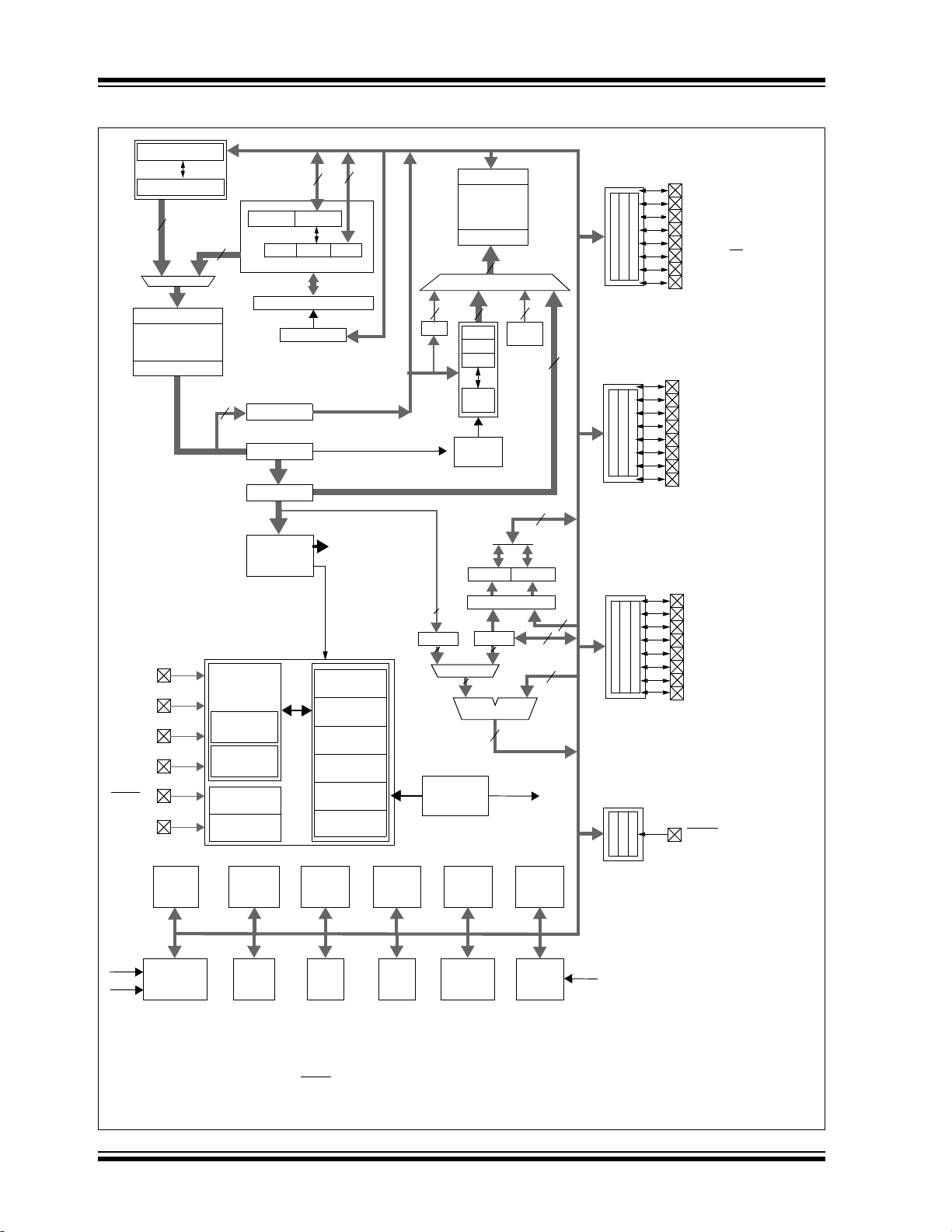
Devices in the PIC18F2XK20/4XK20 family are av ailable in 28-pin and 40/44-pin packages. Block diagrams
for the tw o g roups are shown i n Fi gure 1-1 an d
Figure 1-2.
The devices are differentiated from each other in five
ways:
1. Flash program me mory (8 Kbytes for
PIC18F23K20/43K20 de vices, 16 Kbytes for
PIC18F24K20/44K20 de vices, 32 Kbytes for
PIC18F25K20/45K20 AN D 64 Kbytes for
PIC18F26K20/46K20).
2. A/D channels (11 for 28-pin devices, 14 for
40/44-pin devices).
3. I/O ports (3 bidirectional ports on 28-pin devices,
5 bidirectional ports on 40/44-pin devices).
4. Parallel Sl ave Port (p resent only on 4 0/44-pin
devices).
All other features for devices in this family are identical.
These are summarized in Table 1-1.
The pinouts for all devices are listed in the pin summary
tables: Table 1 and Table 2, and I/O description tables:
Table 1-2 and Table 1-3.
DS41303G-page 12 2010 Microchip Technology Inc.

2010 Microchip Technology Inc. DS41303G-page 13
TABLE 1-1: DEVICE FEATURES
Features PIC18F23K20 PIC18F24K20 PIC18F25K20 PIC18F26K20 PIC18F43K20 PIC18F44K20 PIC18F45K20 PIC18F46K20
Operating Frequency
Program Memory (Bytes) 8192 16384 32768 65536 8192 16384 32768 65536
Program Memory
(Instructions)
Data Memory (Bytes) 512 768 1536 3936 512 768 1536 3936
Data EEPROM Memory
(Bytes)
Interrupt Sources 19 19 19 19 20 20 20 20
I/O Ports A, B, C, (E)
Timers 4 4 44 44 44
Capture/Compare/PWM
Modules
Enhanced Capture/
Compare/PWM Modules
Serial Communications MSSP, Enhanced
Parallel Communications (PSP)
10-bit Analog-to-Digital
Module
Resets (and Delays) POR, BOR, RESET
Programmable High/
Low-Voltage Detect
Programmable Brownout Reset
Instruction Set 75 Instructions; 83
Packages 28-pin PDIP
Note 1: PORTE contains the single RE3 read-only bit. The LATE and TRISE registers are not implemented.
2: Frequency range shown applies to industrial range devices only. Maximum frequency for extended range devices is 48 MHz.
(2)
DC – 64 MHz DC – 64 MHz DC – 64 MHz DC – 64 MHz DC – 64 MHz DC – 64 MHz DC – 64 MHz DC – 64 MHz
USART
1 internal plus 10
Input Channels
Instruction, Stack
Full, Stack Underflow
(PWRT, OST),
MCLR
with Extended
Instruction Set
enabled
28-pin SOIC
28-pin QFN
28-pin SSOP
28-pin UQFN
4096 8192 16384 32768 4096 8192 16384 32768
256 256 256 1024 256 256 256 1024
(1)
11111111
1 1 11 11 11
No No No No Yes Yes Yes Yes
(optional),
WDT
Yes Ye s Yes Ye s Yes Ye s Ye s Yes
Yes Ye s Yes Ye s Yes Ye s Ye s Yes
A, B, C, (E)
MSSP, Enhanced
1 internal plus 10
Input Channels
POR, BOR, RESET
Instruction, Stack
Full, Stack Underflow
(PWRT, OST), MCLR
(optional), WDT
75 Instructions; 83
with Extended
Instruction Set
28-pin PDIP
28-pin SOIC
28-pin QFN
28-pin SSOP
USART
enabled
(1)
MSSP, Enhanced
1 internal plus 10
POR, BOR, RESET
Instruction, Stack
Full, Stack Underflow
75 Instructions; 83
A, B, C, (E)
USART
Input Channels
(PWRT, OST),
MCLR
(optional),
WDT
with Extended
Instruction Set
enabled
28-pin PDIP
28-pin SOIC
28-pin QFN
28-pin SSOP
(1)
MSSP, Enhanced
1 internal plus 10
POR, BOR, RESET
Instruction, Stack
Full, Stack Underflow
(PWRT, OST), MCLR
75 Instructions; 83
A, B, C, (E)
Input Channels
(optional), WDT
with Extended
Instruction Set
28-pin PDIP
28-pin SOIC
28-pin QFN
28-pin SSOP
(1)
USART
enabled
A, B, C, D, E A, B, C, D, E A, B, C, D, E A, B, C, D, E
MSSP, Enhanced
USART
1 internal plus 13
Input Channels
POR, BOR, RESET
Instruction, Stack
Full, Stack Underflow
(PWRT, OST),
MCLR
(optional),
WDT
75 Instructions; 83
with Extended
Instruction Set
enabled
40-pin PDIP
44-pin QFN
44-pin TQFP
MSSP, Enhanced
USART
1 internal plus 13
Input Channels
POR, BOR, RESET
Instruction, Stack
Full, Stack Underflow
(PWRT, OST),
MCLR
(optional),
WDT
75 Instructions; 83
with Extended
Instruction Set
enabled
40-pin PDIP
44-pin QFN
44-pin TQFP
MSSP, Enhanced
USART
1 internal plus 13
Input Channels
POR, BOR, RESET
Instruction, Stack
Full, Stack Underflow
(PWRT, OST),
MCLR
(optional),
WDT
75 Instructions; 83
with Extended
Instruction Set
enabled
40-pin PDIP
44-pin QFN
44-pin TQFP
POR, BOR, RESET
Full, Stack Underflow
(PWRT, OST), MCLR
MSSP, Enhanced
USART
1 internal plus 13
Input Channels
Instruction, Stack
(optional), WDT
75 Instructions; 83
with Extended
Instruction Set
enabled
40-pin PDIP
44-pin QFN
44-pin TQFP
PIC18F2XK20/4XK20
PIC18F2XK20/4XK20
Instruction
Decode and
Control
PORTA
PORTB
PORTC
RA4/T0CKI/C1OUT
RA5/AN4/SS
/HLVDIN/C2OUT
RB0/INT0/FLT0/AN12
RC0/T1OSO/T13CKI
RC1/T1OSI/CCP2
(1)
RC2/CCP1
RC3/SCK/SCL
RC4/SDI/SDA
RC5/SDO
RC6/TX/CK
RC7/RX/DT
RA3/AN3/VREF+
RA2/AN2/VREF-/CVREF
RA1/AN1
RA0/AN0
RB1/INT1/AN10/C12IN3-
Data Latch
Data Memory
Address Latch
Data Address<12>
12
Access
BSR
FSR0
FSR1
FSR2
inc/dec
logic
Address
4
12
4
PCH PCL
PCLATH
8
31-Level Stack
Program Counter
PRODLPRODH
8 x 8 Multiply
8
BITOP
8
8
ALU<8>
20
8
8
Table Pointer<21>
inc/dec logic
21
8
Data Bus<8>
Table Latch
8
IR
12
3
ROM Latch
RB2/INT2/AN8
RB3/AN9/CCP2
(1)
/C12IN2-
PCLATU
PCU
OSC2/CLKOUT
(3)
/RA6
Note 1: CCP2 is multiplexed with RC1 when Configuration bit CCP2MX is set, or RB3 when CCP2MX is not set.
2: RE3 is only available when MCLR
functionality is disabled.
3: OSC1/CLKIN and OSC2/CLKOUT are only available in select oscillator modes and when these pins are not being used as digital I/O.
Refer to Section 2.0 “Oscillator Module (With Fail-Safe Clock Monitor)” for additional information.
RB4/KBI0/AN11
RB5/KBI1/PGM
RB6/KBI2/PGC
RB7/KBI3/PGD
EUSARTComparator
MSSP
10-bit
ADC
Timer2Timer1 Timer3Timer0
CCP2
HLVD
ECCP1
BOR
Data
EEPROM
W
Instruction Bus <16>
STKPTR
Bank
8
State machine
control signals
Decode
8
8
Power-up
Timer
Oscillator
Start-up Timer
Power-on
Reset
Watchdog
Timer
OSC1
(3)
OSC2
(3)
VDD,
Brown-out
Reset
Internal
Oscillator
Fail-Safe
Clock Monitor
Precision
Reference
Band Gap
V
SS
MCLR
(2)
Block
LFINTOSC
Oscillator
16 MHz
Oscillator
Single-Supply
Programming
In-Circuit
Debugger
T1OSO
OSC1/CLKIN
(3)
/RA7
T1OSI
PORTE
MCLR/VPP/RE3
(2)
FVR
FVR
FVR
CVREF
Address Latch
Program Memory
(8/16/32/64 Kbytes)
Data Latch
FIGURE 1-1: PIC18F2XK20 (28-PIN) BLOCK DIAGRAM
DS41303G-page 14 2010 Microchip Technology Inc.

PIC18F2XK20/4XK20
Instruction
Decode and
Control
Data Latch
Data Memory
Address Latch
Data Address<12>
12
Access
BSR
FSR0
FSR1
FSR2
inc/dec
logic
Address
4
12
4
PCH PCL
31-Level Stack
Program Counter
PRODLPRODH
8 x 8 Multiply
8
BITOP
8
8
ALU<8>
Address Latch
Program Memory
(8/16/32/64 Kbytes)
Data Latch
20
8
8
Table Pointer<21>
inc/dec logic
21
Data Bus<8>
Table Latch
8
IR
12
3
ROM Latch
PORTD
RD0/PSP0
PCU
PORTE
MCLR/VPP/RE3
(2)
RE2/CS/AN7
RE0/RD/AN5
RE1/WR/AN6
Note 1: CCP2 is multiplexed with RC1 when Configuration bit CCP2MX is set, or RB3 when CCP2MX is not set.
2: RE3 is only available when MCLR
functionality is disabled.
3: OSC1/CLKIN and OSC2/CLKOUT are only available in select oscillator modes and when these pins are not being used as digital I/O.
Refer to Section 2.0 “Oscillator Module (With Fail-Safe Clock Monitor)” for additional information.
EUSARTComparator
MSSP
10-bit
ADC
Timer2Timer1 Timer3Timer0
CCP2
HLVD
ECCP1
BOR
Data
EEPROM
W
Instruction Bus <16>
STKPTR
Bank
8
State machine
control signals
Decode
8
8
Power-up
Time r
Oscillator
Start-up Timer
Power-on
Reset
Watchdog
Time r
OSC1
(3)
OSC2
(3)
VDD,
Brown-out
Reset
Internal
Oscillator
Fail-Safe
Clock Monitor
Precision
Reference
Band Gap
V
SS
MCLR
(2)
Block
LFINTOSC
Oscillator
16 MHz
Oscillator
Single-Supply
Programming
In-Circuit
Debugger
T1OSI
T1OSO
RD1/PSP1
RD2/PSP2
RD3/PSP3
PORTA
PORTB
PORTC
RA4/T0CKI/C1OUT
RA5/AN4/SS
/HLVDIN/C2OUT
RB0/INT0/FLT0/AN12
RC0/T1OSO/T13CKI
RC1/T1OSI/CCP2
(1)
RC2/CCP1/P1A
RC3/SCK/SCL
RC4/SDI/SDA
RC5/SDO
RC6/TX/CK
RC7/RX/DT
RA3/AN3/VREF+
RA2/AN2/VREF-/CVREF
RA1/AN1
RA0/AN0
RB1/INT1/AN10/C12IN3RB2/INT2/AN8
RB3/AN9/CCP2
(1)
/C12IN2-
OSC2/CLKOUT
(3)
/RA6
RB4/KBI0/AN11
RB5/KBI1/PGM
RB6/KBI2/PGC
RB7/KBI3/PGD
OSC1/CLKIN
(3)
/RA7
RD4/PSP4
RD5/PSP5/P1B
RD6/PSP6/P1C
RD7/PSP7/P1D
FVR
FVR
PSP
FVR
CVREF
PCLATH
8
8
PCLATU
FIGURE 1-2: PIC18F4XK20 (40/44-PIN) BLOCK DIAGRAM
2010 Microchip Technology Inc. DS41303G-page 15

PIC18F2XK20/4XK20
TABLE 1-2: PIC18F2XK20 PINOUT I/O DESCRIPTIONS
Pin Number
Pin Name
MCLR
/VPP/RE3
MCLR
VPP
RE3
OSC1/CLKIN/RA7
OSC1
CLKIN
RA7
OSC2/CLKOUT/RA6
OSC2
CLKOUT
RA6
Legend: TTL = TTL compatible input CMOS = CMOS compatible input or output
ST = Schmitt Trigger input with CMOS levels I = Input
O = Output P = Power
Note 1: Default assignment for CCP2 when Configuration bit CCP2MX is set.
2: Alternate assignment for CCP2 when Configuration bit CCP2MX is cleared.
PDIP,
SOIC
126
96
10 7
QFN
Pin
Type
I
P
I
I
I
I/O
O
O
I/O
Buffer
Type
ST
ST
ST
CMOS
TTL
—
—
TTL
Description
Master Clear (input) or programming voltage (input)
Active-low Master Clear (device Reset) input
Programming voltage input
Digital input
Oscillator crystal or external clock input
Oscillator crystal input or external clock source input
ST buffer when configured in RC mode; CMOS otherwise
External clock source input. Always associated with pin
function OSC1. (See related OSC1/CLKIN, OSC2/CLKOUT
pins)
General purpose I/O pin
Oscillator crystal or clock output
Oscillator crystal output. Connects to crystal or
resonator in Crystal Oscillator mode
In RC mode, OSC2 pin outputs CLKOUT which has 1/4 the
frequency of OSC1 and denotes the instruction cycle rate
General purpose I/O pin
DS41303G-page 16 2010 Microchip Technology Inc.

PIC18F2XK20/4XK20
TABLE 1-2: PIC18F2XK20 PINOUT I/O DESCRIPTIONS (CONTINUED)
Pin Number
Pin Name
RA0/AN0/C12IN0-
RA0
AN0
C12IN0-
RA1/AN1/C12IN1-
RA1
AN1
C12IN1-
RA2/AN2/V
C2IN+
RA2
AN2
V
CV
C2IN+
RA3/AN3/V
RA3
AN3
V
C1IN+
RA4/T0CKI/C1OUT
RA4
T0CKI
C1OUT
RA5/AN4/SS
C2OUT
RA5
AN4
SS
HLVDIN
C2OUT
RA6 See the OSC2/CLKOUT/RA6 pin
RA7 See the OSC1/CLKIN/RA7 pin
Legend: TTL = TTL compatible input CMOS = CMOS compatible input or output
Note 1: Default assignment for CCP2 when Configuration bit CCP2MX is set.
REF-/CVREF/
REF-
REF
REF+/C1IN+
REF+
/HLVDIN/
ST = Schmitt Trigger input with CMOS levels I = Input
O = Output P = Power
2: Alternate assignment for CCP2 when Configuration bit CCP2MX is cleared.
PDIP,
SOIC
QFN
227
328
41
52
63
74
Pin
Type
I/O
I
I
I/O
I
I
I/O
I
I
O
I
I/O
I
I
I
I/O
I
O
I/O
I
I
I
O
Buffer
Type
TTL
Analog
Analog
TTL
Analog
Analog
TTL
Analog
Analog
Analog
Analog
TTL
Analog
Analog
Analog
ST
ST
CMOS
TTL
Analog
TTL
Analog
CMOS
Description
PORTA is a bidirectional I/O port.
Digital I/O
Analog input 0, ADC channel 0
Comparators C1 and C2 inverting input
Digital I/O
ADC input 1, ADC channel 1
Comparators C1 and C2 inverting input
Digital I/O
Analog input 2, ADC channel 2
A/D reference voltage (low) input
Comparator reference voltage output
Comparator C2 non-inverting input
Digital I/O
Analog input 3, ADC channel 3
A/D reference voltage (high) input
Comparator C1 non-inverting input
Digital I/O
Timer0 external clock input
Comparator C1 output
Digital I/O
Analog input 4, ADC channel 4
SPI slave select input
High/Low-Voltage Detect input
Comparator C2 output
2010 Microchip Technology Inc. DS41303G-page 17

PIC18F2XK20/4XK20
TABLE 1-2: PIC18F2XK20 PINOUT I/O DESCRIPTIONS (CONTINUED)
Pin Number
Pin Name
RB0/INT0/FLT0/AN12
RB0
INT0
FLT0
AN12
RB1/INT1/AN10/C12IN3/P1C
RB1
INT1
AN10
C12IN3P1C
RB2/INT2/AN8/P1B
RB2
INT2
AN8
P1B
RB3/AN9/C12IN2-/CCP2
RB3
AN9
C12IN2-
(2)
CCP2
RB4/KBI0/AN11/P1D
RB4
KBI0
AN11
P1D
RB5/KBI1/PGM
RB5
KBI1
PGM
RB6/KBI2/PGC
RB6
KBI2
PGC
RB7/KBI3/PGD
RB7
KBI3
PGD
Legend: TTL = TTL compatible input CMOS = CMOS compatible input or output
ST = Schmitt Trigger input with CMOS levels I = Input
O = Output P = Power
Note 1: Default assignment for CCP2 when Configuration bit CCP2MX is set.
2: Alternate assignment for CCP2 when Configuration bit CCP2MX is cleared.
PDIP,
SOIC
21 18
22 19
23 20
24 21
25 22
26 23
27 24
28 25
QFN
Pin
Type
I/O
I
I
I
I/O
I
I
I
O
I/O
I
I
O
I/O
I
I
I/O
I/O
I
I
O
I/O
I
I/O
I/O
I
I/O
I/O
I
I/O
Buffer
Type
TTL
ST
ST
Analog
TTL
ST
Analog
Analog
CMOS
TTL
ST
Analog
CMOS
TTL
Analog
Analog
ST
TTL
TTL
Analog
CMOS
TTL
TTL
ST
TTL
TTL
ST
TTL
TTL
ST
Description
PORTB is a bidirectional I/O port. PORTB can be software
programmed for internal weak pull-up on each input.
Digital I/O
External interrupt 0
PWM Fault input for CCP1
Analog input 12, ADC channel 12
Digital I/O
External interrupt 1
Analog input 10, ADC channel 10
Comparators C1 and C2 inverting input
Enhanced CCP1 PWM output
Digital I/O
External interrupt 2
Analog input 8, ADC channel 8
Enhanced CCP1 PWM output
Digital I/O
Analog input 9, ADC channel 9
Comparators C1 and C2 inverting input
Capture 2 input/Compare 2 output/PWM 2 output
Digital I/O
Interrupt-on-change pin
Analog input 11, ADC channel 11
Enhanced CCP1 PWM output
Digital I/O
Interrupt-on-change pin
Low-Voltage ICSP™ Programming enable pin
Digital I/O
Interrupt-on-change pin
In-Circuit Debugger and ICSP™ programming clock pin
Digital I/O
Interrupt-on-change pin
In-Circuit Debugger and ICSP™ programming data pin
DS41303G-page 18 2010 Microchip Technology Inc.

PIC18F2XK20/4XK20
TABLE 1-2: PIC18F2XK20 PINOUT I/O DESCRIPTIONS (CONTINUED)
Pin Number
Pin Name
RC0/T1OSO/T13CKI
RC0
T1OSO
T13CKI
RC1/T1OSI/CCP2
RC1
T1OSI
(1)
CCP2
RC2/CCP1/P1A
RC2
CCP1
P1A
RC3/SCK/SCL
RC3
SCK
SCL
RC4/SDI/SDA
RC4
SDI
SDA
RC5/SDO
RC5
SDO
RC6/TX/CK
RC6
TX
CK
RC7/RX/DT
RC7
RX
DT
RE3 — — — — See MCLR
V
SS 8, 19 5, 16 P — Ground reference for logic and I/O pins
DD 20 17 P — Positive supply for logic and I/O pins
V
Legend: TTL = TTL compatible input CMOS = CMOS compatible input or output
ST = Schmitt Trigger input with CMOS levels I = Input
O = Output P = Power
Note 1: Default assignment for CCP2 when Configuration bit CCP2MX is set.
2: Alternate assignment for CCP2 when Configuration bit CCP2MX is cleared.
PDIP,
SOIC
11 8
12 9
13 10
14 11
15 12
16 13
17 14
18 15
QFN
Pin
Buffer
Type
Type
I/O
O
I
I/O
I
Analog
I/O
I/O
I/O
O
CMOS
I/O
I/O
I/O
I/O
I
I/O
I/OOST
I/O
O
I/O
I/O
I
I/O
PORTC is a bidirectional I/O port.
ST
—
ST
ST
ST
ST
ST
ST
ST
ST
ST
ST
ST
—
ST
—
ST
ST
ST
ST
Digital I/O
Timer1 oscillator output
Timer1/Timer3 external clock input
Digital I/O
Timer1 oscillator input
Capture 2 input/Compare 2 output/PWM 2 output
Digital I/O
Capture 1 input/Compare 1 output
Enhanced CCP1 PWM output
Digital I/O
Synchronous serial clock input/output for SPI mode
Synchronous serial clock input/output for I
Digital I/O
SPI data in
2
C™ data I/O
I
Digital I/O
SPI data out
Digital I/O
EUSART asynchronous transmit
EUSART synchronous clock (see related RX/DT)
Digital I/O
EUSART asynchronous receive
EUSART synchronous data (see related TX/CK)
/VPP/RE3 pin
Description
2
C™ mode
2010 Microchip Technology Inc. DS41303G-page 19

PIC18F2XK20/4XK20
TABLE 1-3: PIC18F4XK20 PINOUT I/O DESCRIPTIONS
Pin Name
/VPP/RE3
MCLR
MCLR
VPP
RE3
OSC1/CLKIN/RA7
OSC1
CLKIN
RA7
OSC2/CLKOUT/RA6
OSC2
CLKOUT
RA6
Legend: TTL = TTL compatible input CMOS = CMOS compatible input or output
ST = Schmitt Trigger input with CMOS levels I = Input
O = Output P = Power
Note 1: Default assignment for CCP2 when Configuration bit CCP2MX is set.
2: Alternate assignment for CCP2 when Configuration bit CCP2MX is cleared.
Pin Number
PDIP QFN TQFP
11818
13 32 30
14 33 31
Pin
Type
I
P
I
I
I
I/O
O
O
I/O
Buffer
Type
ST
ST
ST
CMOS
TTL
—
—
TTL
Description
Master Clear (input) or programming voltage (input)
Active-low Master Clear (device Reset) input
Programming voltage input
Digital input
Oscillator crystal or external clock input
Oscillator crystal input or external clock source input
ST buffer when configured in RC mode;
analog otherwise
External clock source input. Always associated with
pin function OSC1 (See related OSC1/CLKIN,
OSC2/CLKOUT pins)
General purpose I/O pin
Oscillator crystal or clock output
Oscillator crystal output. Connects to crystal
or resonator in Crystal Oscillator mode
In RC mode, OSC2 pin outputs CLKOUT which
has 1/4 the frequency of OSC1 and denotes
the instruction cycle rate
General purpose I/O pin
DS41303G-page 20 2010 Microchip Technology Inc.

PIC18F2XK20/4XK20
TABLE 1-3: PIC18F4XK20 PINOUT I/O DESCRIPTIONS (CONTINUED)
Pin Name
RA0/AN0/C12IN0-
RA0
AN0
C12IN0-
RA1/AN1/C12IN0-
RA1
AN1
C12IN0-
RA2/AN2/V
C2IN+
RA3/AN3/V
C1IN+
RA4/T0CKI/C1OUT
RA5/AN4/SS
C2OUT
RA6 See the OSC2/CLKOUT/RA6 pin
RA7 See the OSC1/CLKIN/RA7 pin
Legend: TTL = TTL compatible input CMOS = CMOS compatible input or output
Note 1: Default assignment for CCP2 when Configuration bit CCP2MX is set.
REF-/CVREF/
RA2
AN2
REF-
V
REF
CV
C2IN+
REF+/
RA3
AN3
VREF+
C1IN+
RA4
T0CKI
C1OUT
/HLVDIN/
RA5
AN4
SS
HLVDIN
C2OUT
ST = Schmitt Trigger input with CMOS levels I = Input
O = Output P = Power
2: Alternate assignment for CCP2 when Configuration bit CCP2MX is cleared.
Pin Number
PDIP QFN TQFP
21919
32020
42121
52222
62323
72424
Pin
Type
I/O
I
I
I/O
I
I
I/O
I
I
O
I
I/O
I
I
I
I/O
I
O
I/O
I
I
I
O
Buffer
Type
TTL
Analog
Analog
TTL
Analog
Analog
TTL
Analog
Analog
Analog
Analog
TTL
Analog
Analog
Analog
ST
ST
CMOS
TTL
Analog
TTL
Analog
CMOS
Description
PORTA is a bidirectional I/O port.
Digital I/O
Analog input 0, ADC channel 0
Comparator C1 and C2 inverting input
Digital I/O
Analog input 1, ADC channel 1
Comparator C1 and C2 inverting input
Digital I/O
Analog input 2, ADC channel 2
A/D reference voltage (low) input
Comparator reference voltage output
Comparator C2 non-inverting input
Digital I/O
Analog input 3, ADC channel 3
A/D reference voltage (high) input
Comparator C1 non-inverting input
Digital I/O
Timer0 external clock input
Comparator C1 output
Digital I/O
Analog input 4, ADC channel 4
SPI slave select input
High/Low-Voltage Detect input
Comparator C2 output
2010 Microchip Technology Inc. DS41303G-page 21

PIC18F2XK20/4XK20
TABLE 1-3: PIC18F4XK20 PINOUT I/O DESCRIPTIONS (CONTINUED)
Pin Name
RB0/INT0/FLT0/AN12
RB0
INT0
FLT0
AN12
RB1/INT1/AN10/
C12IN3-
RB1
INT1
AN10
C12IN3-
RB2/INT2/AN8
RB2
INT2
AN8
RB3/AN9/C12IN2-/
CCP2
RB3
AN9
C12IN23-
(2)
CCP2
RB4/KBI0/AN11
RB4
KBI0
AN11
RB5/KBI1/PGM
RB5
KBI1
PGM
RB6/KBI2/PGC
RB6
KBI2
PGC
RB7/KBI3/PGD
RB7
KBI3
PGD
Legend: TTL = TTL compatible input CMOS = CMOS compatible input or output
ST = Schmitt Trigger input with CMOS levels I = Input
O = Output P = Power
Note 1: Default assignment for CCP2 when Configuration bit CCP2MX is set.
2: Alternate assignment for CCP2 when Configuration bit CCP2MX is cleared.
Pin Number
PDIP QFN TQFP
33 9 8
34 10 9
35 11 10
36 12 11
37 14 14
38 15 15
39 16 16
40 17 17
Pin
Type
I/O
I
I
I
I/O
I
I
I
I/O
I
I
I/O
I
I
I/O
I/O
I
I
I/O
I
I/O
I/O
I
I/O
I/O
I
I/O
Buffer
Type
TTL
ST
ST
Analog
TTL
ST
Analog
Analog
TTL
ST
Analog
TTL
Analog
Analog
ST
TTL
TTL
Analog
TTL
TTL
ST
TTL
TTL
ST
TTL
TTL
ST
Description
PORTB is a bidirectional I/O port. PORTB can be
software programmed for internal weak pull-up on
each input.
Digital I/O
External interrupt 0
PWM Fault input for Enhanced CCP1
Analog input 12, ADC channel 12
Digital I/O
External interrupt 1
Analog input 10, ADC channel 10
Comparator C1 and C2 inverting input
Digital I/O
External interrupt 2
Analog input 8, ADC channel 8
Digital I/O
Analog input 9, ADC channel 9
Comparator C1 and C2 inverting input
Capture 2 input/Compare 2 output/PWM 2 output
Digital I/O
Interrupt-on-change pin
Analog input 11, ADC channel 11
Digital I/O
Interrupt-on-change pin
Low-Voltage ICSP™ Programming enable pin
Digital I/O
Interrupt-on-change pin
In-Circuit Debugger and ICSP™ programming
clock pin
Digital I/O
Interrupt-on-change pin
In-Circuit Debugger and ICSP™ programming
data pin
DS41303G-page 22 2010 Microchip Technology Inc.

PIC18F2XK20/4XK20
TABLE 1-3: PIC18F4XK20 PINOUT I/O DESCRIPTIONS (CONTINUED)
Pin Name
RC0/T1OSO/T13CKI
RC0
T1OSO
T13CKI
RC1/T1OSI/CCP2
RC1
T1OSI
(1)
CCP2
RC2/CCP1/P1A
RC2
CCP1
P1A
RC3/SCK/SCL
RC3
SCK
SCL
RC4/SDI/SDA
RC4
SDI
SDA
RC5/SDO
RC5
SDO
RC6/TX/CK
RC6
TX
CK
RC7/RX/DT
RC7
RX
DT
Legend: TTL = TTL compatible input CMOS = CMOS compatible input or output
ST = Schmitt Trigger input with CMOS levels I = Input
O = Output P = Power
Note 1: Default assignment for CCP2 when Configuration bit CCP2MX is set.
2: Alternate assignment for CCP2 when Configuration bit CCP2MX is cleared.
Pin Number
PDIP QFN TQFP
15 34 32
16 35 35
17 36 36
18 37 37
23 42 42
24 43 43
25 44 44
26 1 1
Pin
Buffer
Type
I/O
O
I
I/O
I
CMOS
I/O
I/O
I/O
O
I/O
I/O
I/O
I/O
I
I/O
I/OOST
I/O
O
I/O
I/O
I
I/O
Type
PORTC is a bidirectional I/O port.
ST
—
ST
ST
ST
ST
ST
—
ST
ST
ST
ST
ST
ST
—
ST
—
ST
ST
ST
ST
Digital I/O
Timer1 oscillator output
Timer1/Timer3 external clock input
Digital I/O
Timer1 oscillator input
Capture 2 input/Compare 2 output/PWM 2 output
Digital I/O
Capture 1 input/Compare 1 output/PWM 1 output
Enhanced CCP1 output
Digital I/O
Synchronous serial clock input/output for
SPI mode
Synchronous serial clock input/output for I
Digital I/O
SPI data in
2
C™ data I/O
I
Digital I/O
SPI data out
Digital I/O
EUSART asynchronous transmit
EUSART synchronous clock (see related RX/DT)
Digital I/O
EUSART asynchronous receive
EUSART synchronous data (see related TX/CK)
Description
2
C™ mode
2010 Microchip Technology Inc. DS41303G-page 23

PIC18F2XK20/4XK20
TABLE 1-3: PIC18F4XK20 PINOUT I/O DESCRIPTIONS (CONTINUED)
Pin Name
RD0/PSP0
RD0
PSP0
RD1/PSP1
RD1
PSP1
RD2/PSP2
RD2
PSP2
RD3/PSP3
RD3
PSP3
RD4/PSP4
RD4
PSP4
RD5/PSP5/P1B
RD5
PSP5
P1B
RD6/PSP6/P1C
RD6
PSP6
P1C
RD7/PSP7/P1D
RD7
PSP7
P1D
Legend: TTL = TTL compatible input CMOS = CMOS compatible input or output
ST = Schmitt Trigger input with CMOS levels I = Input
O = Output P = Power
Note 1: Default assignment for CCP2 when Configuration bit CCP2MX is set.
2: Alternate assignment for CCP2 when Configuration bit CCP2MX is cleared.
Pin Number
PDIP QFN TQFP
19 38 38
20 39 39
21 40 40
22 41 41
27 2 2
28 3 3
29 4 4
30 5 5
Pin
Buffer
Type
Type
I/O
I/OSTTTL
I/O
I/OSTTTL
I/O
I/OSTTTL
I/O
I/OSTTTL
I/O
I/OSTTTL
I/O
I/O
TTL
O
I/O
I/O
TTL
O
I/O
I/O
TTL
O
Description
PORTD is a bidirectional I/O port or a Parallel Slave
Port (PSP) for interfacing to a microprocessor port.
These pins have TTL input buffers when PSP module
is enabled.
Digital I/O
Parallel Slave Port data
Digital I/O
Parallel Slave Port data
Digital I/O
Parallel Slave Port data
Digital I/O
Parallel Slave Port data
Digital I/O
Parallel Slave Port data
ST
—
ST
—
ST
—
Digital I/O
Parallel Slave Port data
Enhanced CCP1 output
Digital I/O
Parallel Slave Port data
Enhanced CCP1 output
Digital I/O
Parallel Slave Port data
Enhanced CCP1 output
DS41303G-page 24 2010 Microchip Technology Inc.

PIC18F2XK20/4XK20
TABLE 1-3: PIC18F4XK20 PINOUT I/O DESCRIPTIONS (CONTINUED)
Pin Name
RE0/RD
RE1/WR/AN6
RE2/CS/AN7
RE3 — — — — — See MCLR
VSS 12, 31 6, 30, 316, 29 P — Ground reference for logic and I/O pins
/AN5
RE0
RD
AN5
RE1
WR
AN6
RE2
CS
AN7
Pin Number
PDIP QFN TQFP
82525
92626
10 27 27
Pin
Type
I/O
I
I
I/O
I
I
I/O
I
I
Buffer
Type
ST
TTL
Analog
ST
TTL
Analog
ST
TTL
Analog
Description
PORTE is a bidirectional I/O port
Digital I/O
Read control for Parallel Slave Port
(see related WR
Analog input 5, ADC channel 5
Digital I/O
Write control for Parallel Slave Port
(see related CS
Analog input 6, ADC channel 6
Digital I/O
Chip Select control for Parallel Slave Port
(see related RD
Analog input 7, ADC channel 7
/VPP/RE3 pin
and CS pins)
and RD pins)
and WR)
V
DD 11, 32 7, 8,
28, 29
NC — 13 12, 13,
Legend: TTL = TTL compatible input CMOS = CMOS compatible input or output
ST = Schmitt Trigger input with CMOS levels I = Input
O = Output P = Power
Note 1: Default assignment for CCP2 when Configuration bit CCP2MX is set.
2: Alternate assignment for CCP2 when Configuration bit CCP2MX is cleared.
7, 28 P — Positive supply for logic and I/O pins
— — No connect
33, 34
2010 Microchip Technology Inc. DS41303G-page 25

PIC18F2XK20/4XK20
NOTES:
DS41303G-page 26 2010 Microchip Technology Inc.

PIC18F2XK20/4XK20
4 x PLL
FOSC<3:0>
Secondary Oscillator
T1OSCEN
Enable
Oscillator
T1OSO
T1OSI
Clock Source Option
for other Modules
OSC1
OSC2
Sleep
HSPLL, HFINTOSC/PLL
LP, XT, HS, RC, EC
T1OSC
CPU
Peripherals
IDLEN
Postscaler
MUX
MUX
16 MHz
8 MHz
4 MHz
2 MHz
1 MHz
250 kHz
500 kHz
OSCCON<6:4>
111
110
101
100
011
010
001
000
31 kHz
31 kHz
Source
Internal
Oscillator
Block
WDT, PWRT, FSCM
16 MHz
Internal Oscillator
(HFINTOSC)
Clock
Control
OSCCON<1:0>
Source
16 MHz
31 kHz (LFINTOSC)
OSCTUNE<6>
(1)
0
1
OSCTUNE<7>
and Two-Speed Start-up
Primary Oscillator
PIC18F2XK20/4XK20
Sleep
Sleep
Main
FOSC<3:0> O SCCON<1:0>
Note 1: Operates only when HFINTOSC is the primary oscillator.
2.0 OSCILLATOR MODULE (WITH FAIL-SAFE CLOCK MONITOR)
2.1 Overview
The O scillator m odule has a wide va riety o f cl ock
sources and selection features that allow it to be used
in a wide range of applications while maximizing performance and minimizing power consumption. Figure 2-1
illustrates a block diagram of the Oscillator module.
Clock sources ca n be con figured from external
oscillators, quartz crystal resonators, ceramic resonators
and R esistor-Capacitor (R C) c ircuits. In a ddition, the
system clock source can be configured from one of two
internal oscillators, with a choice of speeds selectable via
software. Additional clock features include:
• Selectable system clock source between external
or internal via software.
• Two-Speed Start-up mode, which minimizes
latency between external oscillator start-up and
code execution.
• Fail-Safe Clock Monitor (FSCM) designed to
detect a failure of the external clock source (LP,
XT, HS, EC or RC modes) and switch
automatically to the internal oscillator.
The Oscillator module can be configured in one of ten
primary clock modes.
1. LP Low-Power Crystal
2. XT Crystal/Resonator
3. HS High-Speed Crystal/Resonator
4. HSPLL High-Speed Crystal/Resonator
with PLL enabled
5. RC External Resistor/Capacitor with
OSC/4 output on RA6
F
6. RCIO External Resistor/Capacitor with I/O
on RA6
7. INTOSC Internal Oscillator with F
OSC/4
output on RA6 and I/O on RA7
8. INTOSCIO Internal Oscillator with I/O on RA6
and RA7
9. EC External Clock with F
OSC/4 output
10. ECIO External Clock with I/O on RA6
Primary Clock modes are selected by the FOSC<3:0>
bits of t he CONFIG1H C onfiguration R egister. T he
HFINTOSC and LFINTOSC are factory calibrated highfrequency and low-frequency oscillators, respectively,
which are used as the internal clock sources.
FIGURE 2-1: PIC® MCU CLOCK SOURCE BLOCK DIAGRAM
2010 Microchip Technology Inc. DS41303G-page 27

PIC18F2XK20/4XK20
2.2 Oscillator Control
The OSCCON register (Register 2-1) controls several
aspects o f the dev ice c lock’s op eration, bo th in ful l
power operation and in power-managed modes.
• Main System Clock Selection (SCS)
• Internal Frequency selection bits (IRCF)
• Clock Status bits (OSTS, IOFS)
• Power management selection (IDLEN)
2.2.1 MAIN SYSTEM CLOCK SELECTION
The Sy stem Cloc k Se lect b its, SCS<1 :0>, s elect th e
main clock source. The available clock sources are
• Primary clock defined by the FOSC<3:0> bits of
CONFIG1H. The primary clock can be the primary
oscillator, an external clock, or the internal oscillator block.
• Secondary clock (Timer1 oscillator)
• Internal oscillator block (HFINTOSC and
LFINTOSC).
The c lock s ource cha nges i mmediately af ter one or
more of the bits is written to, following a brief clock transition interval. The SCS bits are cl eared to sel ect the
primary clock on all forms of Reset.
2.2.4 CLOCK STATUS
The OSTS and IOFS bits of the OSCCON register, and
the T1RUN bit of the T1CON register, indicate which
clock source is currently providing the main clock. The
OSTS b it i ndicates th at th e O scillator S tart-up T imer
has timed out and the primary clock is p roviding the
device clock. The IOFS bit indicates when the internal
oscillator b lock has stabilized a nd is p roviding th e
device cl ock i n H FINTOSC C lock m odes. The IO FS
and O STS S tatus bit s w ill bo th b e s et w hen
SCS<1:0> = 00 and HFINTOSC is the primary clock.
The T1RUN bit indicates when the Timer1 oscillator is
providing the device clock in secondary clock modes.
When SCS<1:0> 00, only one of these three bits will
be set at any time. If none of the se bits are set, th e
LFINTOSC is providing the clock or the H FINTOSC
has just started and is not yet stable.
2.2.5 POWER MANAGEMENT
The IDLEN bit of the OSCCON register determines if
the d evice go es into Sle ep mode o r on e of the Idl e
modes when the SLEEP instruction is executed.
The use of the flag and control bits in the OSCCON
register i s di scussed in m ore d etail in Section 3.0
“Power-Managed Modes”.
2.2.2 INTERNAL FREQUENCY
SELECTION
The Int ernal Os cillator Frequency Se lect bit s
(IRCF<2:0>) select the frequency output of the internal
oscillator block. The choices are the LFINTOSC source
(31 kHz), the HFINTOSC so urce (16 MHz) or one of
the freq uencies de rived from the H FINTOSC pos tscaler (31 .25 kHz to 8 MHz). If the internal oscillator
block is supplying the main clock, changing the states
of th ese b its w ill ha ve an i mmediate c hange on th e
internal oscillator’s output. On device Resets, the output f requency of the in ternal oscillator is s et t o th e
default frequency of 1 MHz.
2.2.3 LOW FREQUENCY SELECTION
When a nominal output frequency of 31 kHz is selected
(IRCF<2:0> = 000), users may choose which internal
oscillator ac ts as th e s ource. Thi s i s done w ith th e
INTSRC bit of the OSCTUNE register. Setting this bit
selects the HFINTOSC as a 31.25 kHz clock source by
enabling the di vide-by-512 ou tput of the H FINTOSC
postscaler. Clearing INTSRC selects LFINTOSC (nominally 31 kHz) as the clock source.
This option allows users to select the tunable and more
precise HFINTOSC as a clock source, while maintaining power savings with a very low clock speed. Regardless of t he se tting of I NTSRC, LFINTOSC a lways
remains th e c lock source fo r fea tures s uch a s th e
Watchdog Timer and the Fail-Safe Clock Monitor.
Note 1: The Timer1 oscillator must be enabled to
select the secondary c lock so urce. Th e
Timer1 oscillator is enabled by setting the
T1OSCEN b it of the T1 CON re gister. If
the Timer1 oscillator is not enabled, then
the m ain osc illator w ill c ontinue to ru n
from the previously selected source. The
source will then switch to the secondary
oscillator after the T1OSCEN bit is set.
2: It i s rec ommended tha t the Timer1
oscillator be operating and stable before
selecting the secondary clock source or a
very lo ng delay ma y o ccur while th e
Timer1 oscillator starts.
DS41303G-page 28 2010 Microchip Technology Inc.

PIC18F2XK20/4XK20
REGISTER 2-1: OSCCON: OSCILLATOR CONTROL REGISTER
R/W-0 R/W-0 R/W-1 R/W-1 R-q R-0 R/W-0 R/W-0
IDLEN IRCF2 IRCF1 IRCF0 OSTS
bit 7 bit 0
Legend:
R = Readable bit W = Writable bit U = Unimplemented bit, read as ‘0’ q = depends on condition
-n = Value at POR ‘1’ = Bit is set ‘0’ = Bit is cleared x = Bit is unknown
bit 7 IDLEN: Idle Enable bit
1 = Device enters Idle mode on SLEEP instruction
0 = Device enters Sleep mode on SLEEP instruction
bit 6-4 IRCF<2:0>: Internal Oscillator Frequency Select bits
111 = 16 MHz (HFINTOSC drives clock directly)
110 = 8 MHz
101 = 4 MHz
100 = 2 MHz
011 = 1 MHz
010 = 500 kHz
001 = 250 kHz
000 = 31 kHz (from either HFINTOSC/512 or LFINTOSC directly)
bit 3 OSTS: Oscillator Start-up Time-out Status bit
1 = Device is running from the clock defined by FOSC<2:0> of the CONFIG1 register
0 = Device is running from the internal oscillator (HFINTOSC or LFINTOSC)
bit 2 IOFS: HFINTOSC Frequency Stable bit
1 = HFINTOSC frequency is stable
0 = HFINTOSC frequency is not stable
bit 1-0 SCS<1:0>: System Clock Select bits
1x = Internal oscillator block
01 = Secondary (Timer1) oscillator
00 = Primary clock (determined by CONFIG1H[FOSC<3:0>]).
(3)
(1)
(1)
IOFS SCS1 SCS0
(2)
Note 1: Reset state depends on state of the IESO Configuration bit.
2: Source selected by the INTSRC bit of the OSCTUNE register, see text.
3: Default output frequency of HFINTOSC on Reset.
2010 Microchip Technology Inc. DS41303G-page 29

PIC18F2XK20/4XK20
OSC1/CLKIN
OSC2/CLKOUT
(1)
I/O
Clock from
Ext. System
PIC
®
MCU
Note 1: Alternate pin functions are listed in
Section 1.0 “Device Overview”.
2.3 Clock Source Modes
Clock Source modes can be classified as external or
internal.
• External Clock modes rely on external circuitry for
the clock source. Examples are: Clock modules
(EC mode), quartz crystal resonators or ceramic
resonators (LP, XT and HS modes) and ResistorCapacitor (RC mode) circuits.
• Internal clock sources are contained internally
within the Oscillator block. The Oscillator block
has two internal oscillators: the 16 MHz HighFrequency Internal Oscillator (HFINTOSC) and
the 31 kHz Low-Frequency Internal Oscillator
(LFINTOSC).
The system clock can be selected between external or
internal cl ock sources vi a the S ystem Cl ock S elect
(SCS<1:0>) b its o f the OSCCO N register. Se e
Section 2.9 “Clock Switching” for additional informa-
tion.
2.4 External Clock Modes
2.4.1 OSCILLATOR START-UP TIMER (OST)
When the Oscillator module is configured for LP, XT or
HS modes, the Oscillator Start-up Timer (OST) counts
1024 oscillations from O SC1. Thi s occurs following a
Power-on Reset (POR) and when the Power-up Timer
(PWRT) has expired (if configured), or a wake-up from
Sleep. During this time, the program counter does not
increment and program execution is suspended. The
OST ensures that the oscillator circuit, using a quartz
crystal resonator or ceramic resonator, has started and
is prov iding a stable system clo ck to the Oscillator
module. W hen swi tching be tween cl ock s ources, a
delay i s required to al low the new cl ock to s tabilize.
These oscillator delays are shown in Table 2-1.
In order to minimize latency between external oscillator
start-up a nd c ode ex ecution, the T wo-Speed C lock
Start-up mo de can be se lected (see Section 2.10
“Two-Speed Clock Start-up Mode”).
TABLE 2-1: OSCILLATOR DELAY EXAMPLES
Switch From Switch To Frequency Oscillator Delay
Sleep/POR
Sleep/POR EC, RC DC – 64 MHz 2 instruction cycles
LFINTOSC (31 kHz) EC, RC DC – 64 MHz 1 cycle of each
Sleep/POR LP, XT, HS 32 kHz to 40 MHz 1024 Clock Cycles (OST)
Sleep/POR HSPLL 32 MHz to 64 MHz 1024 Clock Cycles (OST) + 2 ms
LFINTOSC (31 kHz) HFINTOSC 250 kHz to 16 MHz 1 s (approx.)
LFINTOSC
HFINTOSC
31 kHz
250 kHz to 16 MHz
Oscillator Warm-Up Delay (T
WARM)
2.4.2 EC MODE
The Ext ernal C lock ( EC) mode al lows an ext ernally
generated logic level as the system clock source. When
operating in this mode , a n ext ernal clock sour ce is
connected to the OSC1 input and the OSC2 is available
for ge neral p urpose I /O. Fig ure 2-2 s hows th e pi n
connections for EC mode.
The Oscillator Start-up Timer (OST) is disabled when
EC mode is selected. Therefore, there is no delay in
operation af ter a Power-on R eset (POR) or wake-up
from Sleep. B ecause t he PIC
static, sto pping t he external clock input w ill have the
effect of halting the device while leaving all data intact.
Upon res tarting the external cl ock, th e dev ice w ill
resume operation as if no time had elapsed.
DS41303G-page 30 2010 Microchip Technology Inc.
®
MCU de sign is fully
FIGURE 2-2: EXTERNAL CLOCK (EC)
MODE OPERATION

PIC18F2XK20/4XK20
Note 1: A seri es resistor (R S) may be required for
quartz crystals with low drive level.
2: The value of R
F varies with the Oscillator mode
selected (typically between 2 M to 10 M.
C1
C2
Quartz
R
S
(1)
OSC1/CLKIN
RF
(2)
Sleep
To Internal
Logic
PIC® MCU
Crystal
OSC2/CLKOUT
Note 1: A series res istor (R S) may be re quired f or
ceramic resonators with low drive level.
2: The value of R
F varies with the Oscillator mode
selected (typically between 2 M to 10 M.
3: An addit ional p arallel f eedback resis tor (R
P)
may be required for proper cer amic resonator
operation.
C1
C2
Ceramic
R
S
(1)
OSC1/CLKIN
RF
(2)
Sleep
To Internal
Logic
PIC® MCU
RP
(3)
Resonator
OSC2/CLKOUT
2.4.3 LP, XT, HS MODES
The LP, XT and HS modes support the use of quartz
crystal resonators or ceramic resonators connected to
OSC1 and OSC2 (Figure 2-3). The mode selects a low,
medium o r h igh ga in setting of the in ternal inverteramplifier to support various resonator types and speed.
LP Oscillator mode selects the lowest gain setting of the
internal inverter-amplifier. LP mode current consumption
is the least of the three modes. This mode is best suited
to drive resonators with a low drive level specification, for
example, tuning fork type crystals.
XT Oscillator mode s elects t he intermediate g ain
setting of the internal in verter-amplifier. XT mode
current consumption is the medium of the three modes.
This m ode is be st s uited to drive re sonators w ith a
medium drive level specification.
HS Oscillator mode selects the highest gain setting of the
internal inverter-amplifier. HS mode current consumption
is the h ighest of th e three modes. This mode is be st
suited for resonators that require a high drive setting.
Figure 2-3 a nd Figure 2-4 show ty pical c ircuits for
quartz crystal and ceramic resonators, respectively.
FIGURE 2-3: QUARTZ CRYSTAL
OPERATION (LP, XT OR
HS MODE)
Note 1: Quartz crystal characteristics vary according
to ty pe, p ackage and manu facturer. Th e
user s hould consult t he manufacturer data
sheets for specifications and recommended
application.
2: Always verify oscillator performance over
DD an d t emperature ran ge that i s
the V
expected for the application.
3: For oscillator design assistance, reference
the following Microchip Applications Notes:
• AN826, “Crystal Oscillator Basics and
Crystal Selection for rfPIC
®
and PIC®
Devices” (DS00826)
®
• AN849, “Basic PIC
Oscillator Design”
(DS00849)
®
• AN943, “Practical PIC
Oscillator
Analysis and Design” (DS00943)
• AN949, “Making Your Oscillator Work”
(DS00949)
FIGURE 2-4: CERAMIC RESONATOR
OPERATION
(XT OR HS MODE)
2010 Microchip Technology Inc. DS41303G-page 31

PIC18F2XK20/4XK20
OSC2/CLKOUT
(1)
CEXT
REXT
PIC® MCU
OSC1/CLKIN
F
OSC/4 or
Internal
Clock
VDD
VSS
Recommended values: 10 k REXT 100 k
C
EXT > 20 pF
Note 1: Alternate pin functions are listed in
Section 1.0 “Device Overview”.
2: Output depends upon RC or RCIO clock mode.
I/O
(2)
2.4.4 EXTERNAL RC MODES
The external Resistor-Capacitor (RC) modes support
the u se of an external R C c ircuit. T his al lows th e
designer maximum flexibility in frequency choice while
keeping costs to a minimum when clock accuracy is not
required. There are two modes: RC and RCIO.
2.4.4.1 RC Mode
In RC mode, the RC circuit connects to OSC1. OSC2/
CLKOUT outputs the R C oscillator frequency divided
by 4. This si gnal ma y be used to provide a cl ock for
external c ircuitry, s ynchronization, c alibration, t est or
other application req uirements. Figure 2-5 shows the
external RC mode connections.
FIGURE 2-5: EXTERNAL RC MODES
2.4.4.2 RCIO Mode
In RCIO mode, the RC circuit is connected to OSC1.
OSC2 becomes an additional general purpose I/O pin.
The RC oscillator frequency is a function of the su pply
voltage, the resistor (R
and the operating temp erature. Other factors affecting
the oscillator frequency are:
• input threshold voltage variation
• component tolerances
• packaging variations in capacitance
The user also needs to take into account variation due
to tolerance of external RC components used.
EXT) and capacitor (CEXT) values
2.5 Internal Clock Modes
The O scillator m odule has tw o ind ependent, int ernal
oscillators that c an be c onfigured o r s elected as th e
system clock source.
1. The HFINTOSC (H igh-Frequency Int ernal
Oscillator) is factory calibrated and operates at
16 MHz. The frequency of the HFINTOSC can
be us er-adjusted v ia software using the
OSCTUNE register (Register 2-2).
2. The LFINTOSC (Low -Frequency Internal
Oscillator) operates at 31 kHz.
The system clock speed can be selected via software
using the Internal Oscillator Fre quency Sel ect bit s
IRCF<2:0> of the OSCCON register.
The system clock can be selected between external or
internal clock sources via the System Clock Selection
(SCS<1:0>) bi ts of the O SCCON re gister. Se e
Section 2.9 “Clock Switching” for more information.
2.5.1 INTOSC AND INTOSCIO MODES
The IN TOSC and INTOSCIO m odes co nfigure the
internal os cillators as th e p rimary cl ock s ource. Th e
FOSC<3:0> bi ts i n t he C ONFIG1H Configuration
register determine w hich m ode i s selected. Se e
Section 23.0 “Special Features of the CPU” for more
information.
In INTOSC mode, OSC1/CLKIN is available for general
purpose I/O. O SC2/CLKOUT out puts the s elected
internal oscillator frequency divided by 4. The CLKOUT
signal may be used to prov ide a c lock fo r external
circuitry, sy nchronization, ca libration, test or oth er
application requirements.
In INTOSCIO mode, OSC1/CLKIN and OSC2/CLKOUT
are available for general purpose I/O.
2.5.2 HFINTOSC
The output of the HFINTOSC connects to a postscaler
and m ultiplexer ( see Figure 2-1). On e of eight
frequencies ca n be selec ted via s oftware us ing the
IRCF<2:0> bit s of the O SCCON register . See
Section 2.5.4 “Frequency Select Bits (IRCF)” for
more information.
The HFINTOSC is enabled when:
•SCS1 = 1 and IRCF<2:0> 000
•SCS1 = 1 and IRCF<2:0> = 000 and INTSRC = 1
• IESO bit of CONFIG1H = 1 enabling Two-Speed
Start-up.
• FCMEM bit of CONFIG1H = 1 enabling Two-
Speed Start-up and Fail-Safe mode.
• FOSC<3:0> of CONFIG1H selects the internal
oscillator as the primary clock
The H F In ternal O scillator (IOFS) bi t o f the O SCCON
register indicates whether the HFINTOSC is stable or not.
DS41303G-page 32 2010 Microchip Technology Inc.

PIC18F2XK20/4XK20
2.5.2.1 OSCTUNE Register
The H FINTOSC is fac tory ca librated b ut c an b e
adjusted in software by writing to the TUN<5:0> bits of
the OSCTUNE register (Register 2-2).
The default value of the TUN<5:0> is ‘ 000000’. Th e
value is a 6-bit two’s complement number.
When the OSC TUNE regis ter i s mod ified, the
HFINTOSC fr equency will be gin shif ting to the new
frequency. C ode ex ecution continues du ring this shift.
There is no indication that the shift has occurred.
OSCTUNE does not af fect the L FINTOSC frequency.
Operation of features that depend on the LF INTOSC
clock source frequency , such as the Power-up Timer
(PWRT), Watchdog Timer (WDT), Fail-Safe Clock Mon-
itor (FS CM) and periphe rals, ar e not af fected by the
change in frequency.
The OSCTUNE register also implements the INTSRC
and PLLEN bits, which control certain features of th e
internal oscillator block.
The INTSRC bit a llows users to select which internal
oscillator provides the clock source when the 31 kHz
frequency option is selected. This is covered in greater
detail in Section 2.2.3 “Low Frequency Selection”.
The PLLEN bit controls the operation of the frequency
multiplier, PLL, in internal oscillator modes. For more
details a bout the function o f t he PLLEN b it see
Section 2.6.2 “PLL in HFINTOSC Modes”
REGISTER 2-2: OSCTUNE: OSCILLATOR TUNING REGISTER
R/W-0 R/W -0 R/W-0 R/W-0 R/W-0 R/W-0 R/W-0 R/W-0
INTSRC PLLEN
bit 7 bit 0
Legend:
R = Readable bit W = Writable bit U = Unimplemented bit, read as ‘0’
-n = Value at POR ‘1’ = Bit is set ‘0’ = Bit is cleared x = Bit is unknown
(1)
TUN5 TUN4 TUN3 TUN2 TUN1 TUN0
bit 7 INTSRC: Internal Oscillator Low-Frequency Source Select bit
1 = 31.25 kHz device clock derived from 16 MHz HFINTOSC source (divide-by-512 enabled)
0 = 31 kHz device clock derived directly from LFINTOSC internal oscillator
bit 6 PLLEN: Frequency Multiplier PLL for HFINTOSC Enable bit
1 = PLL enabled for HFINTOSC (8 MHz and 16 MHz only)
0 = PLL disabled
bit 5-0 TUN<5:0>: Frequency Tuning bits
011111 = Maximum frequency
011110 =
• • •
000001 =
000000 = Oscillator module is running at the factory calibrated frequency.
111111 =
• • •
100000 = Minimum frequency
Note 1: The PLLEN bit is active only when the HFINTOSC is the primary clock source (FOSC<2:0> = 100X) and
the selected frequency is 8 MHz or 16 MHz. Otherwise, the PLLEN bit is unavailable and always reads ‘0’.
(1)
2010 Microchip Technology Inc. DS41303G-page 33

PIC18F2XK20/4XK20
2.5.3 LFINTOSC
The Low-Frequency Internal Oscillator (LFINTOSC) is
a 31 kHz internal clock source.
The out put o f the LFINTOSC con nects to inte rnal
oscillator block freq uency s election mul tiplexer (s ee
Figure 2-1). Sel ect 31 kHz, via s oftware, usi ng the
IRCF<2:0> bit s of th e O SCCON register and the
INTSRC bit of th e O SCTUNE reg ister. See
Section 2.5.4 “Frequency Select Bits (IRCF)” for
more information. The LFINTOSC is also the frequency
for the Power-up T imer (PWRT), W atchdog T imer
(WDT) and Fail-Safe Clock Monitor (FSCM).
The LFINTOSC is enabled when any of the following
are enabled:
• IRCF<2:0> bits of the OSCCON register = 000 and
INTSRC bit of the OSCTUNE register = 0
• Power-up Timer (PWRT)
• Watchdog Timer (WDT)
• Fail-Safe Clock Monitor (FSCM)
2.5.4 FREQUENCY SELECT BITS (IRCF)
The output of t he 16 MHz H FINTOSC an d 3 1 kHz
LFINTOSC co nnects to a postscaler and multiplexer
(see Figure 2-1). The Int ernal Os cillator Fre quency
Select bits IRCF<2:0> of th e OSCCON register select
the output frequency of the internal oscillators. One of
eight frequencies can be selected via software:
•16 MHz
•8 MHz
•4 MHz
•2 MHz
• 1 MHz (Default after Reset)
• 500 kHz
• 250 kHz
• 31 kHz (LFINTOSC or HFINTOSC/512)
Note: Following any Reset, the IRCF<2:0> bits of
the OSCCON register are set to ‘011’ and
the fr equency selection i s s et to 1 MHz.
The use r can modify the IRCF bit s to
select a different frequency.
2.5.5 HFINTOSC FREQUENCY DRIFT
The factory calibrates the internal oscillator block output
(HFINTOSC) for 16 MHz. However, this f requency may
drift as V
controller operation in a var iety of w ays. It is possibl e to
adjust the HFINTOSC frequency by modifying the value
of the TUN<5:0> bits in the OSCTUNE register. This has
no effect on the LFINTOSC clock source frequency.
Tuning the HFINTOSC source requires knowing when to
make the adjus tment, in w hich directio n it should be
made and in some cases, how large a change is
needed. Th ree po ssible c ompensation techniques are
discussed in the following sections, however other techniques may be used.
DD or temperature changes, which can affect the
2.5.5.1 Compensating with the USART
An adj ustment m ay be req uired w hen the USART
begins to generate framing errors or receives data with
errors while in As ynchronous m ode. Framing error s
indicate that the device clock frequency is too high; to
adjust for th is, decrement the value in OSCTUNE to
reduce the clock frequency. On the other hand, errors
in data may suggest that the clock speed is too low; to
compensate, in crement O SCTUNE to inc rease the
clock frequency.
2.5.5.2 Compensating with the Timers
This technique compares device clock speed to some
reference clock. Two timers may be used; one timer is
clocked by the pe ripheral clo ck, w hile the other is
clocked by a fi xed re ference source, s uch as th e
Timer1 oscillator.
Both timers are cleared, but the timer clocked by the
reference gen erates int errupts. Whe n an in terrupt
occurs, th e internally c locked ti mer i s read a nd both
timers are cleared. If the internally clocked timer value
is gre ater th an ex pected, th en the internal osc illator
block is running too fast. To adjust for this, decrement
the OSCTUNE register.
2.5.5.3 Compensating with the CCP Module
in Capture Mode
A CCP module can use free running Timer1 (or Timer3),
clocked b y the internal oscillator block and an external
event w ith a k nown period (i.e., A C power frequency).
The time of the fi rst e vent is c aptured in th e
CCPRxH:CCPRxL registers and is recorded for use later.
When the second event causes a capture, the time of the
first e vent i s subtracted from th e time of th e second
event. Since the period of the external event is known,
the time difference between events can be calculated.
If the mea sured t ime is much greater tha n the calculated time, t he i nternal osci llator bl ock is running to o
fast; to compensate, decrement the OSCTUNE register.
If the measured time is much les s than the calculated
time, the internal oscillator block is running too slow; to
compensate, increment the OSCTUNE register.
DS41303G-page 34 2010 Microchip Technology Inc.

PIC18F2XK20/4XK20
MUX
VCO
Loop
Filter
Crystal
Osc
OSC2
OSC1
PLL Enable
F
IN
FOUT
SYSCLK
Phase
Comparator
HS Oscillator Enable
4
(from Configuration Register 1H)
HS Mode
2.6 PLL Frequency Multiplier
A Phase Locked Loop (PLL) circuit is provided as an
option fo r us ers w ho w ish to u se a lo wer fre quency
oscillator circuit or to clock the device up to its highest
rated frequency from the crystal oscillator. This may be
useful for customers who are concerned with EMI due
to high-frequency crystals or users who require higher
clock sp eeds f rom an i nternal os cillator. Th ere a re
three conditions when the PLL can be used:
• When the primary clock is HSPLL
• When the primary clock is HFINTOSC and the
selected frequency is 16 MHz
• When the primary clock is HFINTOSC and the
selected frequency is 8 MHz
2.6.1 HSPLL OSCILLATOR MODE
The HSPLL mode makes use of the HS mode oscillator
for frequencies up to 16 MHz. A PLL then multiplies the
oscillator output frequency by 4 to produce an internal
clock frequency up to 64 MHz. The PLLEN bit of the
OSCTUNE register is active only when the HFINTOSC
is the primary clock and is not available in HSPLL oscillator mode.
The PLL is only available to the primary oscillator when
the FOSC<3:0> Configuration bits are programmed for
HSPLL mode (= 0110).
2.6.2 PLL IN HFINTOSC MODES
The 4x frequency multiplier can be used with the internal o scillator blo ck to p roduce fas ter d evice cl ock
speeds than are norm ally possible w ith an int ernal
oscillator. Whe n ena bled, th e PLL pro duces a cl ock
speed of up to 64 MHz.
Unlike H SPLL mo de, the PLL is controlled through
software. T he PL LEN co ntrol bi t of t he O SCTUNE
register is used to enable or disable the PLL operation
when the HFINTOSC is used.
The PLL is availa ble when the devi ce is configured to
use t he internal osc illator bloc k as it s p rimary cloc k
source (FOSC<3:0> = 1001 or 1000). Additionally, the
PLL w ill only func tion w hen t he selected output frequency is either 8 MHz or 16 MHz (O SCCON<6:4> =
111 or 110). If both of these conditions are not met, the
PLL is disabled.
The PLLEN control bit is only functional in those internal oscillator modes where the PLL is available. In all
other m odes, it i s fo rced to ‘ 0’ an d is ef fectively
unavailable.
FIGURE 2-6: PLL BLOCK DIAGRAM
(HS MODE)
2010 Microchip Technology Inc. DS41303G-page 35

PIC18F2XK20/4XK20
2.7 Effects of Power-Managed Modes on the Various Clock Sources
For more information about the modes discussed in this
section see Section 3.0 “Power-Managed Modes”. A
quick reference list is also available in Table 3-1.
When PRI_IDLE mode is selected, the designated primary oscillator continues to run w ithout int erruption.
For a ll other p ower-managed modes, t he oscillator
using the OSC1 pi n is disabled. The OSC1 pin (and
OSC2 pin, if used by the oscillator) will stop oscillating.
In se condary clock mo des (SEC_RUN a nd
SEC_IDLE), th e T imer1 oscillator is ope rating an d
providing the device clock. The Timer1 oscillator may
also run in al l po wer-managed mo des if required to
clock Timer1 or Timer3.
In internal o scillator m odes (INT OSC_RUN a nd
INTOSC_IDLE), t he internal oscillator b lock p rovides
the device clock source. The 31 kHz LFINTOSC output
can be used directly to provide the clock and may be
enabled to support various special features, regardless
of th e power-managed m ode (s ee Section 23.2
“Watchdog Timer (WDT)”, Section 2.10 “TwoSpeed Clock S t art-up Mo de” and Se ction 2.11 “FailSafe Clock Monitor” fo r m ore in formation on W DT,
Fail-Safe Clock Monitor and Two-Speed Start-up). The
HFINTOSC output at 16 MHz may be used directly to
clock the device or may be divided down by the postscaler. The HFINTOSC output is disabled if the clock is
provided directly from the LFINTOSC output.
If the Slee p m ode is se lected, al l c lock sou rces a re
stopped. Si nce all th e transistor s witching currents
have been stopped, Sleep mode achieves the lowest
current c onsumption of the de vice (only l eakage
currents).
Enabling any on- chip fe ature tha t will operate d uring
Sleep will increase the current consumed during Sleep.
The LFINTOSC is required to support WDT operation.
The T imer1 o scillator may be operating to s upport a
real-time clock. Other features may be operating that
do not require a device clock source (i.e., SSP s lave,
PSP, INTn pins and others). Peripherals that may add
significant cu rrent consumption are li sted in
Section 26.8 “DC Characteristics”.
2.8 Power-up Delays
Power-up delays are controlled by two timers, so that
no external Reset circuitry is required for most applications. The de lays ensure t hat the d evice i s k ept i n
Reset until the device power supply is stable under normal circumstances and the primary clock is operating
and s table. Fo r ad ditional information o n p ower-up
delays, see Section 4.5 “Device Reset Timers”.
The first timer is the Power-up Timer (PWRT), w hich
provides a f ixed de lay on pow er-up (parameter 3 3,
Table 26-10). It i s en abled by c learing (= 0) th e
PWRTEN
The s econd tim er i s t he O scillator S tart-up T imer
(OST), i ntended to ke ep the ch ip in Res et un til th e
crystal oscillator is stable (LP, XT and HS modes). The
OST d oes th is by co unting 10 24 o scillator c ycles
before allowing the oscillator to clock the device.
When the H SPLL O scillator m ode i s selected, th e
device is kept in Reset for an additional 2 ms, following
the HS mode OST delay, s o the PLL can lock to th e
incoming clock frequency.
There is a del ay of in terval T
Table 26-10), fol lowing POR, w hile th e c ontroller
becomes ready to execute instructions. This delay runs
concurrently w ith any oth er del ays. Th is may be the
only delay that occurs when any of the EC, RC or INTIO
modes are used as the primary clock source.
When the HFINTOSC is selected as the primary clock,
the ma in s ystem cl ock ca n be delayed un til th e
HFINTOSC is st able. This is us er sel ectable by the
HFOFST bit o f the CONFIG3H Configuration register.
When the HFOFST bit is cleared the main system clock
is de layed u ntil t he H FINTOSC is sta ble. W hen t he
HFOFST bit is set the main system clock starts immediately. In either case the IOFS bit of the OSCCON register can be read to determine whether the HFINTOSC
is operating and stable.
Configuration bit.
CSD (pa rameter 38,
TABLE 2-2: OSC1 AND OSC2 PIN STATES IN SLEEP MODE
OSC Mode OSC1 Pin OSC2 Pin
RC, INTOSC Floating, external resistor should pull high At logic low (clock/4 output)
RCIO Floating, external resistor should pull high Configured as PORTA, bit 6
INTOSCIO Configured as PORTA, bit 7 Configured as PORTA, bit 6
ECIO Floating, pulled by external clock Configured as PORTA, bit 6
EC Floating, pulled by external clock At logic low (clock/4 output)
LP, XT, HS and HSPLL Feedback inverter disabled at quiescent
voltage level
Note: See Table 4-2 in Section 4.0 “Reset” for time-outs due to Sleep and MCLR
DS41303G-page 36 2010 Microchip Technology Inc.
Feedback inverter disabled at quiescent
voltage level
Reset.

PIC18F2XK20/4XK20
2.9 Clock Switching
The s ystem cl ock s ource c an b e sw itched b etween
external and internal clock sources via software using
the S ystem C lock S elect (SCS<1:0>) b its of the
OSCCON register.
PIC18F2XK20/4XK20 devices contain circuitry to prevent c lock “glitches” when s witching b etween clock
sources. A short pause in the device clock occurs during the clock switch. The length of this pause is the sum
of two cycles of the old clock source and three to four
cycles of the new clock source. This formula assumes
that the new clock source is stable.
Clock t ransitions a re discussed in gre ater de tail i n
Section 3.1.2 “Entering Power-Managed Modes”.
2.9.1 SYSTEM CLOCK SELECT (SCS<1:0>) BITS
The Sys tem Clock Sele ct (SC S<1:0>) bi ts o f the
OSCCON register select the system clock source that
is used for the CPU and peripherals.
• When SCS<1:0> = 00, the system clock source is
determined by configuration of the FOSC<2:0>
bits in the CONFIG1H Configuration register.
• When SCS<1:0> = 10, the system clock source is
chosen by the internal oscillator frequency
selected by the INTSRC bit of the OSCTUNE
register and the IRCF<2:0> bits of the OSCCON
register.
• When SCS<1:0> = 01, the system clock source is
the 32.768 kHz secondary oscillator shared with
Timer1.
After a Reset, th e SC S<1:0> bits o f the OSCCON
register are always cleared.
Note: Any automa tic clock sw itch, whi ch may
occur from Two-Speed Start-up or Fail-Safe
Clock Mon itor, does not upd ate the
SCS<1:0> bi ts of the O SCCON register.
The user can monitor the T1RUN bit of the
T1CON register and the IOFS and OSTS
bits of the OSCCON register to determine
the current system clock source.
2.9.3 CLOCK SWITCH TIMING
When sw itching bet ween one oscillator and ano ther,
the new oscillator may not be op erating which saves
power (see Figure 2-7). If th is is th e c ase, the re is a
delay after the SCS<1:0> bits of the OSCCON register
are modified before the frequency change takes place.
The OSTS and IOFS bits of the OSCCON register will
reflect the current ac tive s tatus of th e ex ternal an d
HFINTOSC o scillators. The t iming of a frequency
selection is as follows:
1. SCS<1:0> bits of the OSCCON register are modified.
2. The old clock continues to operate until the new
clock is ready.
3. Clock switch circuitry waits for two consecutive
rising edges of the old clock after the new clock
ready signal goes true.
4. The system clock is held low starting at the next
falling edge of the old clock.
5. Clock switch circuitry waits for an additional two
rising edges of the new clock.
6. On the next falling edge of the new clock the low
hold on the system clock is released and new
clock is switched in as the system clock.
7. Clock switch is complete.
See Figure 2-1 for more details.
If the HFINTOSC is the source of both the old and new
frequency, th ere is no st art-up d elay before the n ew
frequency is active. This is because the old and new
frequencies are der ived fro m the H FINTOSC via the
postscaler and multiplexer.
Start-up de lay sp ecifications are located in
Section 26.0 “Electrical Characteristics”, under AC
Specifications (Oscillator Module).
2.9.2 OSCILLATOR START-UP TIME-OUT STATUS (OSTS) BIT
The Oscillator Start-up T ime-out Status (OSTS) bit of
the OSCCON register in dicates w hether the sy stem
clock is run ning from the ex ternal cl ock source, a s
defined b y t he F OSC<3:0> bi ts in t he C ONFIG1H
Configuration re gister, o r fro m the in ternal clock
source. In particular, when the primary oscillator is the
source of th e p rimary cl ock, OSTS indicates that the
Oscillator Start-up Timer (OST) has timed out for LP,
XT or HS modes.
2010 Microchip Technology Inc. DS41303G-page 37

PIC18F2XK20/4XK20
2.10 Two-Speed Clock Start-up Mode
Two-Speed S tart-up m ode pro vides a dditional po wer
savings b y m inimizing th e la tency bet ween ext ernal
oscillator start-up and code execution. In applications
that make heavy use of the Sleep mode, Two-Speed
Start-up w ill rem ove the external os cillator s tart-up
time fro m the tim e spent aw ake and c an red uce th e
overall power consumption of the device.
This mode a llows th e app lication to w ake-up fr om
Sleep, perform a few instructions using the HFINTOSC
as t he cl ock sou rce and g o ba ck to S leep w ithout
waiting for the primary oscillator to become stable.
Note: Executing a SLEEP ins truction w ill abo rt
the oscillator start-up t ime a nd will cause
the OSTS bi t of the OSCCON register to
remain clear.
When the Oscillator module is configured for LP, XT or
HS mode s, th e Oscilla tor S tart-up Timer (OS T) is
enabled (see Section 2.4.1 “Oscillator Start-up Timer
(OST)”). The OST will suspend program execution until
1024 osc illations ar e co unted. T wo-Speed S tart-up
mode mi nimizes the delay i n code e xecution b y
operating from the in ternal oscill ator as t he OST is
counting. When the OST count reaches 1024 and the
OSTS bit of the O SCCON regis ter i s set, program
execution switches to the external oscillator.
2.10.2 TWO-SPEED START-UP SEQUENCE
1. Wake-up from Power-on Reset or Sleep.
2. Instructions b egin e xecuting by the int ernal
oscillator at the frequency set in the IRCF<2:0>
bits of the OSCCON register.
3. OST e nabled to count 1 024 ex ternal cl ock
cycles.
4. OST timed out. External clock is ready.
5. OSTS is set.
6. Clock switch finishes according to FIGURE 2-7:
“Clock Switch Timing”
2.10.3 CHECKING TWO-SPEED CLOCK STATUS
Checking t he s tate of t he OS TS b it of the OSCCON
register will c onfirm if th e m icrocontroller is running
from the ex ternal cl ock so urce, as defined by t he
FOSC<2:0> bits in CONFIG1H Configuration register,
or the internal oscillator. OSTS = 0 when the external
oscillator is not ready, which indicates that the system
is running from the internal oscillator.
2.10.1 TWO-SPEED START-UP MODE CONFIGURATION
Two-Speed Start-up mode is enabled when all of the
following settings are configured as noted:
• Two-Speed Start-up mode is enabled by setting
the IESO of the CONFIG1H Configuration register
is set. Fail-Safe mode (FCMEM = 1) also enables
two-speed by default.
• SCS<1:0> (of the OSCCON register) = 00.
• FOSC<2:0> bits of the CONFIG1H Configuration
register are configured for LP, XT or HS mode.
Two-Speed Start-up mode becomes active after:
• Power-on Reset (POR) and, if enabled, after
Power-up Timer (PWRT) has expired, or
• Wake-up from Sleep.
If th e ext ernal clock oscillator is co nfigured to be
anything ot her t han LP, XT or HS m ode, t hen T woSpeed S tart-up is d isabled. This is be cause t he
external clock o scillator does n ot re quire a ny
stabilization time after POR or an exit from Sleep.
DS41303G-page 38 2010 Microchip Technology Inc.

FIGURE 2-7: CLOCK SWITCH TIMING
Old Clock
New Clock
IRCF <2:0>
System Clock
Start-up Time
(1)
Clock Sync Running
High Speed Low Speed
Select Old
Select New
New Clk Ready
Low Speed High Speed
Old Clock
New Clock
IRCF <2:0>
System Clock
Start-up Time
(1)
Clock Sync Running
Select Old Select New
New Clk Ready
Note 1: Start-up time includes TOST (1024 TOSC) for external clocks, plus TPLL (approx. 2 ms) for HSPLL mode.
PIC18F2XK20/4XK20
2010 Microchip Technology Inc. DS41303G-page 39

PIC18F2XK20/4XK20
External
LFINTOSC
÷ 64
S
R
Q
31 kHz
(~32 s)
488 Hz
(~2 ms)
Clock Monitor
Latch
Clock
Failure
Detected
Oscillator
Clock
Q
Sample Clock
2.11 Fail-Safe Clock Monitor
The Fail-Safe Clock Monitor (FSCM) allows the device
to continue operating should the external oscillator fail.
The FSCM can detect oscillator failure any time after
the Oscillator Start-up Timer (OST) has expired. The
FSCM is enabled by s etting th e F CMEN bit in th e
CONFIG1H C onfiguration register. The FSC M i s
applicable to all external oscillator modes (LP, XT, HS,
EC, RC and RCIO).
FIGURE 2-8: FSCM BLOCK DIAGRAM
2.11.1 FAIL-SAFE DETECTION
The FS CM m odule dete cts a fai led os cillator b y
comparing the external oscillator to the FSCM sample
clock. The s ample cl ock is generated by dividing the
LFINTOSC by 64. See Figure 2-8. Ins ide the fai l
detector block is a latc h. The ex ternal c lock sets the
latch on each fal ling ed ge o f the external cl ock. Th e
sample clock clears the latch on each rising edge of the
sample clock. A failure is detected when an entire halfcycle of the sample clock elapses before the primary
clock goes low.
2.11.3 FAIL-SAFE CONDITION CLEARING
The Fail-Safe condition is cleared by either one of the
following:
•Any Reset
• By toggling the SCS1 bit of the OSCCON register
Both of th ese co nditions re start the OST. Whi le th e
OST is running, the device continues to operate from
the IN TOSC s elected in OS CCON. Wh en th e O ST
times o ut, th e Fa il-Safe con dition is cl eared an d th e
device automatically switches over to the external clock
source. The Fai l-Safe co ndition nee d not be cleared
before the OSCFIF flag is cleared.
2.11.4 RESET OR WAKE-UP FROM SLEEP
The FSCM is designed to detect an os cillator failure
after the Oscillator Start-up Timer (OST) has expired.
The OST is used after waking up from Sleep and after
any type of Reset. The OST is not used with the EC or
RC Clock modes so that the FSCM will be active a s
soon as the Reset or wake-up has completed. When
the FSCM is enabled, the Two-Speed Start-up is also
enabled. Therefore, the device will always be executing
code while the OST is operating.
Note: Due to the wide range of oscillator start-up
times, the Fail-Safe circuit is not ac tive
during oscillator st art-up (i.e., af ter ex iting
Reset or Sleep). Af ter an appropriate
amount of time, the user should check the
OSTS bit of the OSCCON register to verify
the oscillator start-up and that the sys tem
clock sw itchover has succ essfully
completed.
2.11.2 FAIL-SAFE OPERATION
When the external clock fails, the FSCM switches the
device clock to an internal clock source and sets the bit
flag OSCFIF of the PIR2 register. The OSCFIF flag will
generate an int errupt if the OSCFIE bit of th e PIE2
register is also set. The device firmware can then take
steps to mi tigate the problems that may arise from a
failed cl ock. T he s ystem c lock w ill co ntinue t o be
sourced from the internal clock source until the device
firmware s uccessfully re starts the e xternal os cillator
and switches back to external operation. An automatic
transition back to the failed clock source will not occur.
The in ternal cl ock so urce ch osen by the FSC M is
determined by the IRCF<2:0> b its of th e OSC CON
register. Thi s al lows the internal os cillator to be
configured before a failure occurs.
DS41303G-page 40 2010 Microchip Technology Inc.

PIC18F2XK20/4XK20
OSCFIF
System
Clock
Output
Sample Clock
Failure
Detected
Oscillator
Failure
Note: The system clock is normally at a much higher frequency than the sample clock. The relative frequencies in
this example have been chosen for clarity.
(Q)
Te st
Test Test
Clock Monitor Output
FIGURE 2-9: FSCM TIMING DIAGRAM
T ABLE 2-3: SUMMARY OF REGISTERS ASSOCIATED WITH CLOCK SOURCES
Name Bit 7 Bit 6 Bit 5 Bit 4 Bit 3 Bit 2 Bit 1 Bit 0
CONFIG1H IESO FCMEN — — FOSC3 FOSC2 FOSC1 FOSC0 — —
INTCON GIE/GIEH P EIE/GIEL
OSCCON IDLEN IRCF2 IRCF1 IRCF0 OSTS IOFS SCS1 SCS0 0011 q000 0011 q000
OSCTUNE INTSRC PLLEN TUN5 TUN4 TUN3 TUN2 TUN1 TUN0 0000 0000 000u uuuu
PIE2 OSCFIE
PIR2 OSCFIF
IPR2 OSCFIP
Legend: x = unknown, u = unchanged, – = unimplemented locations read as ‘0’. Shaded cells are not used by oscillators.
Note 1: Other (non Power-up) Resets include MCLR
C1IE C2IE EEIE BCLIE HLVDIE TMR3IE CCP2IE 0000 0000 0000 0000
C1IF C2IF EEIF BCLIF HLVDIF TMR3IF CCP2IF 0000 0000 0000 0000
TMR0IE INT0IE RBIE TMR0IF INT0IF RBIF 0000 000x 0000 000x
— — — — — — — 1111 1111 1111 1111
Reset and Watchdog Timer Reset during normal operation.
Val ue on
POR, BOR
Val ue on
all other
Resets
(1)
2010 Microchip Technology Inc. DS41303G-page 41

PIC18F2XK20/4XK20
NOTES:
DS41303G-page 42 2010 Microchip Technology Inc.

PIC18F2XK20/4XK20
3.0 POWER-MANAGED MODES
PIC18F2XK20/4XK20 dev ices of fer a to tal of s even
operating modes fo r m ore e fficient po wer management. The se mo des pro vide a v ariety of op tions for
selective p ower conservation in ap plications w here
resources ma y be lim ited (i.e ., battery-powered
devices).
There are three categories of power-managed modes:
• Run modes
• Idle modes
• Sleep mode
These categories define which portions of the device
are clocked and sometimes, what speed. The Run and
Idle modes m ay us e a ny of the three available clock
sources (pr imary, s econdary or i nternal os cillator
block); the Sleep mode does not use a clock source.
The pow er-managed modes include several pow ersaving features offered on previous PIC
devices. One is the clock switching feature which allows
the controller to use the Timer1 oscillator in place of the
primary oscillator. Also inc luded is the S leep mode,
offered by al l PIC
device clocks are stopped.
®
microcontroller d evices, w here all
3.1 Selecting Power-Managed Modes
Selecting a pow er-managed mode r equires two
decisions:
• Whether or not the CPU is to be clocked
• The selection of a clock source
The IDLEN bit of the OSCCON register controls CPU
clocking, w hile t he S CS<1:0> b its of the OS CCON
register select the clock source. The individual modes,
bit settings, c lock sources a nd affected m odules a re
summarized in Table 3-1.
®
microcontroller
3.1.1 CLOCK SOURCES
The SCS<1:0> bits allow the selection of one of three
clock sources for power-managed modes. They are:
• the primary clock, as defined by the FOSC<3:0>
Configuration bits
• the secondary clock (the Timer1 oscillator)
• the internal oscillator block
3.1.2 ENTERING POWER-MANAGED
MODES
Switching from one power-managed mode to another
begins by lo ading the O SCCON re gister. Th e
SCS<1:0> bits select the clock source and determine
which Run or Idle mode is to be used. Changing these
bits ca uses a n im mediate sw itch to th e ne w cl ock
source, assuming that it is run ning. The switch may
also be s ubject t o clock t ransition d elays. T hese are
discussed in Section 3.1.3 “Clock Transitions and
Status Indicators” and subsequent sections.
Entry to the po wer-managed Idle or S leep mo des is
triggered by the execution of a SLEEP instruction. The
actual mode that results depends on the status of the
IDLEN bit of the OSCCON register.
Depending on the c urrent mod e and the m ode being
switched to, a change to a power-managed mode does
not always require s etting all of the se bi ts. M any
transitions may be done by changing the oscillator select
bits, or changing the IDLEN bit, prior to issuing a SLEEP
instruction. If the ID LEN bit is al ready c onfigured
correctly, it may only be necessary to perform a SLEEP
instruction to switch to the desired mode.
TABLE 3-1: POWER-MANAGED MODES
Mode
Sleep 0 N/A Off Off None – All clocks are disabled
PRI_RUN N/A 00 Clocked Clocked Primary – LP, XT, HS, HSPLL, RC, EC and
SEC_RUN N/A 01 Clocked Clocked Secondary – Timer1 Oscillator
RC_RUN N/A 1x Clocked Clocked Internal Oscillator Block
PRI_IDLE 100Off Clocked Primary – LP, XT, HS, HSPLL, RC, EC
SEC_IDLE 101Off Clocked Secondary – Timer1 Oscillator
RC_IDLE 11xOff Clocked Internal Oscillator Block
Note 1: IDLEN reflects its value when the SLEEP instruction is executed.
2: Includes HFINTOSC and HFINTOSC postscaler, as well as the LFINTOSC source.
2010 Microchip Technology Inc. DS41303G-page 43
OSCCON Bits Module Clocking
(1)
IDLEN
SCS<1:0> CPU Peripherals
Available Clo ck and Os cill ator Sour ce
(2)
Internal Oscillator Block
This is the normal full power execution mode.
.
(2)
(2)

PIC18F2XK20/4XK20
3.1.3 CLOCK TRANSITIONS AND STATUS INDICATORS
The length of the transition between clock sources is
the sum of:
• Start-up time of the new clock
• Two and one half cycles of the old clock source
• Two and one half cycles of the new clock
Three flag bits indicate the current clock source and its
status. They are:
• OSTS (of the OSCCON register)
• IOFS (of the OSCCON register)
• T1RUN (of the T1CON register)
In general, only one of these bits will be set while in a
given power-managed mode. Table 3-2 shows the relationship of the fla gs to the active main system clock
source.
TABLE 3-2: SYSTEM CLOCK INDICATORS
OSTS IOFS T1RUN Main System Clock Source
10 0 Primary Oscillator
01 0 HFINTOSC
00 1 Secondary Oscillator
11 0 HFINTOSC as primary clock
00 0
.
Note 1: Executing a SLEEP instruction does not
necessarily pl ace th e d evice i nto Sleep
mode. It a cts as the t rigger to place th e
controller in to eit her the Sleep mode or
one of the Idle modes, depending on the
setting of the IDLEN bit.
LFINTOSC or
HFINTOSC is not yet stable
3.1.4 MULTIPLE FUNCTIONS OF THE SLEEP COMMAND
The po wer-managed mode tha t is i nvoked w ith the
SLEEP instruction is determined by the s etting of the
IDLEN bit o f the OSCCON regi ster at th e tim e th e
instruction is executed. All c locks sto p an d mi nimum
power is consumed when SLEEP is executed with the
IDLEN bit cleared. The system clock continues to supply a clock to the peripherals but is disconnected from
the CPU when SLEEP is executed with the IDLEN bit
set.
3.2 Run Modes
In the Run m odes, c locks to bot h the co re an d
peripherals are ac tive. Th e dif ference between these
modes is the clock source.
3.2.1 PRI_RUN MODE
The PRI_RUN mode is the normal, full power execution
mode o f th e microcontroller. Th is i s also the default
mode upon a device Reset, unless Two-Speed Start-
up is enabled (see Section 2.10 “Two-Speed Clock
Start-up Mode” for details). In this mode, the OSTS bit
is set. The IOFS bit will be set if the HFINTOSC is the
primary clock source and the oscillator is stable (see
Section 2.2 “Oscillator Control”).
3.2.2 SEC_RUN MODE
The SEC_RUN mo de i s the mode compatible to th e
“clock s witching” f eature offered i n o ther PIC 18
devices. I n thi s m ode, th e C PU and pe ripherals a re
clocked from the Timer1 oscillator. This gives users the
option of lower power consumption w hile still using a
high accuracy clock source.
SEC_RUN mode is entered by setting the SCS<1:0>
bits to ‘01’. When SEC_RUN mode is active all of the
following are true:
• The main clock source is switched to the Timer1
oscillator
• Primary oscillator is shut down
• T1RUN bit of the T1CON register is set
• OSTS bit is cleared.
Note: The T imer1 osc illator sh ould al ready be
running prior to entering SEC_RUN mode.
If t he T1 OSCEN b it is not set when th e
SCS<1:0> bits a re s et t o ‘ 01’, en try to
SEC_RUN mo de will n ot o ccur until
T1OSCEN bit is set and Timer1 oscillator
is ready.
On transitions from SEC_RUN mode to PRI_RUN, the
peripherals and CPU continue to be clocked from the
Timer1 o scillator w hile th e primary clock i s started.
When the primary clock becomes ready, a clock switch
back to th e pri mary c lock oc curs (s ee Fi gure 2-7).
When the clock switch is complete, the T1RUN bit is
cleared, the OSTS bit is set and the primary clock is
providing the main system clock. The Timer1 oscillator
continues to run as long as the T1OSCEN bit is set.
DS41303G-page 44 2010 Microchip Technology Inc.

PIC18F2XK20/4XK20
3.2.3 RC_RUN MODE
In R C_RUN mode, th e C PU a nd p eripherals are
clocked from the internal oscillator block using one of
the selections from the HFINTOSC multiplexer. In this
mode, t he primary osc illator i s shut down. R C_RUN
mode provides the best power conservation of all the
Run m odes w hen the LFINTOSC is the m ain cl ock
source. It works well for user applications which are not
highly timing se nsitive or do no t require hig h-speed
clocks at all times.
If the pri mary clock s ource is the in ternal oscillator
block (either LFINTOSC or HFINTOSC), there are no
distinguishable d ifferences b etween PRI_RUN a nd
RC_RUN modes during e xecution. However, a c lock
switch de lay w ill oc cur du ring ent ry to and exi t fro m
RC_RUN mode. Therefore, if the primary clock source
is the inte rnal os cillator bl ock, th e us e of R C_RUN
mode is not recommended. See 2.9.3 “Clock Switch
Timing” for details about clock switching.
RC_RUN mode is entered by setting the SCS1 bit to
‘1’. The SCS0 bit can be either ‘0’ or ‘1’ but should be
‘0’ to ma intain so ftware co mpatibility w ith futu re
devices. When the clock source is switched from the
primary oscillator to the HFINTOSC multiplexer, the primary os cillator is sh ut do wn an d the OST S bit i s
cleared. The IRCF bits may be modified at any time to
immediately change the clock speed.
On transitions from RC_RUN mode to PRI_RUN mode,
the dev ice co ntinues to be c locked from the internal
oscillator block w hile the pri mary oscillator is st arted.
When the pri mary o scillator b ecomes ready, a cl ock
switch t o t he primary c lock oc curs. Wh en the clock
switch is complete, the IOFS bit is cleared, the OSTS
bit is set and the primary oscillator is providing the main
system clock. The HFINTOSC will continue to run if any
of the conditions noted in Section 2.5.2 “HFINTOSC”
are met. The LFINTOSC source will continue to run if
any of the co nditions noted in Section 2.5.3 “LFIN-
TOSC” are met.
3.3 Sleep Mode
The Power-Managed Sleep mode in the PIC18F2XK20/
4XK20 devices is id entical t o the legacy Sle ep mod e
offered in all oth er PIC
entered by clearing the IDLEN bit (the default state on
device R eset) and execu ting the SLEEP i nstruction.
This shuts down the selected oscillator (Figure 3-1). All
clock source Status bits are cleared.
Entering the Sleep mode from any other mode does not
require a clock switch. This is because no cl ocks are
needed once th e controller has entered Sleep. If the
WDT is selected, the LFINTOSC source will continue to
operate. If the Timer1 oscillator is enabled, it will also
continue to run.
When a wake event occurs in Sleep mode (by interrupt,
Reset or WDT time-out), the device will not be clocked
until the clock source selected by the SCS<1:0> bits
becomes ready (see Figure 3-2), or i t will be clocked
from the internal oscillator block if either the Two-Speed
Start-up or the Fai l-Safe C lock Mo nitor are ena bled
(see Sectio n 23.0 “Special Features of the C PU”). In
either case, the OSTS bit is set when the primary clock
is providing the device clocks. The IDLEN and SCS bits
are not affected by the wake-up.
®
mi crocontroller devi ces. It is
3.4 Idle Modes
The Id le m odes al low th e c ontroller’s C PU to b e
selectively shut down while the peripherals continue to
operate. Selecting a particular Idle mode allows users
to further manage power consumption.
If the IDLEN bit is set to a ‘1’ when a SLEEP instruction is
executed, the peripherals will be clocked from the clock
source selected by the SCS<1:0> bits; however, the CPU
will not be clocked. The clock source Status bits are not
affected. Setting IDLEN and executing a SLEEP instruction provides a quick method of switching from a given
Run mode to its corresponding Idle mode.
If the WDT is selected, the LFINTOSC source will continue to operate. If the Timer1 oscillator is enabled, it
will also continue to run.
Since the CPU is not executing instructions, the only
exits from any of the Idle modes are by interrupt, WDT
time-out, or a Reset. When a wake event occurs, CPU
execution is d elayed by an i nterval of T
(parameter 38, Table 26-10) while it becomes ready to
execute code. When the CPU begins executing code,
it resumes with the same clock source for the current
Idle mode. For example, when waking from RC_IDLE
mode, the in ternal oscillator block will clock the CPU
and peripherals (in other words, RC_RUN mode). The
IDLEN and SCS bits are not affected by the wake-up.
While in an y Idle mode or t he Sleep mode, a WDT
time-out will result in a WDT wake-up to the Run mode
currently specified by the SCS<1:0> bits.
CSD
2010 Microchip Technology Inc. DS41303G-page 45

PIC18F2XK20/4XK20
Q4Q3Q2
OSC1
Peripheral
Sleep
Program
Q1Q1
Counter
Clock
CPU
Clock
PC + 2PC
Q3 Q4 Q1 Q2
OSC1
Peripheral
Program
PC
PLL Clock
Q3 Q4
Output
CPU Clock
Q1 Q2 Q3 Q4 Q1 Q2
Clock
Counter
PC + 6
PC + 4
Q1 Q2 Q3 Q4
Wake Event
Note1: T
OST = 1024 TOSC; TPLL = 2 ms (approx). These intervals are not shown to scale.
TOST
(1)
TPLL
(1)
OSTS bit set
PC + 2
FIGURE 3-1: TRANSITION TIMING FOR ENTRY TO SLEEP MODE
FIGURE 3-2: TRANSITION TIMING FOR WAKE FROM SLEEP (HSPLL)
DS41303G-page 46 2010 Microchip Technology Inc.

PIC18F2XK20/4XK20
Q1
Peripheral
Program
PC PC + 2
OSC1
Q3
Q4
Q1
CPU Clock
Clock
Counter
Q2
OSC1
Peripheral
Program
PC
CPU Clock
Q1 Q3 Q4
Clock
Counter
Q2
Wake Even t
TCSD
3.4.1 PRI_IDLE MODE
This mo de is unique among the three lo w-power Idle
modes, in that it d oes n ot disable the primary device
clock. For timing sensitive applications, this allows for
the fastest resumption of device operation with its more
accurate primary clock source, since the clock source
does not have to “warm-up” or transition from another
oscillator.
PRI_IDLE mo de is ent ered from PR I_RUN m ode by
setting the IDLEN bit and executing a SLEEP instruction. If the device is in another Run mode, set IDLEN
first, then cle ar th e SC S bits and exe cute SLEEP.
Although the CPU is disabled, the peripherals continue
to be clocked from the primary clock source specified
by th e FO SC<3:0> C onfiguration b its. Th e OSTS bit
remains set (see Figure 3.3).
When a wake event occurs, the CPU is clocked from the
primary clock so urce. A delay of in terval T
required between the w ake even t and w hen cod e
execution starts. T his is re quired to allow th e CPU t o
become ready to execute instructions. After the wakeup, the OSTS bit remains set. The IDLEN and SCS bits
are not affected by the wake-up (see Figure 3-4).
CSD is
3.4.2 SEC_IDLE MODE
In SEC_IDLE mo de, the CPU is disabled but the
peripherals continue to be cl ocked from the Timer1
oscillator. This mode is entered from SEC_RUN by setting the IDLEN bit and executing a SLEEP instruction. If
the device is in another Run mode, set the IDLEN bit
first, then set the SCS<1:0> bits to ‘ 01’ a nd execute
SLEEP. When th e clock so urce i s swi tched t o t he
Timer1 oscillator, the pr imary os cillator is shut down,
the OSTS bit is cleared and the T1RUN bit is set.
When a wake event occurs, the peripherals continue to
be clocked from the Timer1 oscillator. After an interval
CSD following the wake event, the CPU begins exe-
of T
cuting code being clocked by the Timer1 oscillator. The
IDLEN and SCS bits are not affected by the wake-up;
the Timer1 oscillator continues to run (see Figure 3-4).
Note: The T imer1 osc illator sh ould al ready be
running prior to entering SEC_IDLE mode.
If th e T1 OSCEN b it is not set wh en th e
SLEEP instruction is ex ecuted, th e m ain
system clock will continue to operate in the
previously sel ected mode and the corresponding IDLE mode will be entered (i.e.,
PRI_IDLE or RC_IDLE).
FIGURE 3-3: TRANSITION TIMING FOR ENTRY TO IDLE MODE
FIGURE 3-4: TRANSITION TIMING FOR WAKE FROM IDLE TO RUN MODE
2010 Microchip Technology Inc. DS41303G-page 47

PIC18F2XK20/4XK20
3.4.3 RC_IDLE MODE
In RC_IDLE mode, the CPU is disabled but the peripherals continue to be clocked from the internal oscillator
block from t he H FINTOSC multiplexer output. Thi s
mode allows for controllable power conservation during
Idle periods.
From RC_RUN, t his mo de i s entered b y setting th e
IDLEN b it an d ex ecuting a SLEEP i nstruction. If th e
device is in another Run mode, first set IDLEN, then set
the SCS1 bit and e xecute SLEEP. It is recommended
that SCS0 al so be cl eared, alt hough its v alue i s
ignored, to maintain software compatibility w ith futu re
devices. The H FINTOSC multiplexer may be used to
select a higher clock frequency by modifying the IRCF
bits before executing the SLEEP instruction. When the
clock source is switched to the HFINTOSC multiplexer,
the primary oscillator is shut down and the OSTS bit is
cleared.
If the IRCF bits are set to a ny non-zero value, or th e
INTSRC bit is set, the HFINTOSC output is e nabled.
The IOFS bit becomes set, after the HFINTOSC output
becomes s table, a fter an inte rval of T
(parameter 39, Table 26-10). Clocks to the peripherals
continue while the HFINTOSC source stabilizes. If the
IRCF b its w ere prev iously a t a n on-zero va lue, or
INTSRC was set before the SLEEP instruction was executed and the HFINTOSC source was already stable,
the I OFS bi t wil l re main set. If the IRCF b its an d
INTSRC are all clear, the HFINTOSC output will not be
enabled, the IOFS bit will remain clear and there will be
no indication of the current clock source.
When a wake event occurs, the peripherals continue to
be c locked from t he HFINTOSC mul tiplexer output.
After a de lay of T
CPU beg ins ex ecuting cod e bei ng clocked by the
HFINTOSC multiplexer. The IDLEN and SCS bits are
not affected by the wake-up. The LFINTOSC s ource
will continue to run if either the WDT or th e Fail-Safe
Clock Monitor is enabled.
CSD fol lowing th e w ake eve nt, the
IOBST
3.5 Exiting Idle and Sleep Modes
An exit from Sleep mode or an y of the Idle modes is
triggered by any one of the following:
• an interrupt
•a Reset
• a watchdog time-out
This section di scusses the triggers that c ause ex its
from power-managed modes. The clocking subsystem
actions are discussed in each of the power-managed
modes ( see Section 3.2 “Run Modes”, Section 3.3
“Sleep Mode” and Section 3.4 “Idle Modes”).
3.5.1 EXIT BY INTERRUPT
Any of the available interrupt so urces can ca use the
device to exit from an Idle mode or the Sleep mode to
a Run mode. To enable this functionality, an interrupt
source must be enabled by setting its enable bit in one
of the INTCON or PIE registers. The PEIE bIt must also
be set If the desired interrupt enable bit is in a PIE register. The ex it s equence i s in itiated w hen the co rresponding interrupt flag bit is set.
The in struction im mediately fo llowing the SLEEP
instruction is executed on all exits by interrupt from Idle
or Sleep modes. Code execution then branches to the
interrupt vector if the GIE/GIEH bit of the INTCON register is set, otherwise code execution continues without
branching (see Sec tion9.0 “Interrupts”).
A fixed delay of interval T
is required when leaving Sleep and Idle modes. This
delay is required for the CPU to prepare for execution.
Instruction execution resumes on the first clock cycle
following this delay.
CSD following the wake event
3.5.2 EXIT BY WDT TIME-OUT
A WDT time-out will cause different actions depending
on which power-managed mode the device is in when
the time-out occurs.
If the device is not executing code (all Idle modes and
Sleep mode), the time-out will result in an exit from the
power-managed m ode (s ee Section 3.2 “Run
Modes” and Section 3.3 “Sleep Mode”). If the device
is ex ecuting co de ( all R un mo des), the t ime-out w ill
result in a WDT Reset (see Section 23.2 “Watchdog
Timer (WDT)”).
The WDT timer and postscaler are cleared by any one
of the following:
• executing a SLEEP instruction
• executing a CLRWDT instruction
• the loss of the currently selected clock source
when the Fail-Safe Clock Monitor is enabled
• modifying the IRCF bits in the OSCCON register
when the internal oscillator block is the device
clock source
3.5.3 EXIT BY RESET
Exiting Sleep an d Id le mo des by Reset causes code
execution to r estart a t ad dress 0. See Section 4.0
“Reset” for more details.
The ex it de lay tim e fro m R eset to the s tart o f code
execution de pends o n both the clock sources before
and after the wake-up and the type of oscillator. Exit
delays are summarized in Table 3-3.
DS41303G-page 48 2010 Microchip Technology Inc.

PIC18F2XK20/4XK20
3.5.4 EXIT WITHOUT AN OSCILLATOR START-UP DELAY
Certain e xits from p ower-managed modes d o n ot
invoke the OST at all. There are two cases:
• PRI_IDLE mode, where the primary clock source
is not stopped and
• the primary clock source is not any of the LP, XT,
HS or HSPLL modes.
In t hese instances, the primary c lock s ource e ither
does not require an oscillator start-up delay since it is
already running (PR I_IDLE), or norm ally does not
require an oscillator start-up delay (RC, EC, INTOSC,
and INT OSCIO mod es). However, a fix ed delay of
interval T
CSD following the wake event is still required
when leaving Sleep and Idle modes to allow the CPU
to prepare for execution. Instruction execution resumes
on the first clock cycle following this delay.
TABLE 3-3: EXIT DELAY ON WAKE-UP BY RESET FROM SLEEP MODE OR ANY IDLE MODE
(BY CLOCK SOURCES)
Clock Source
before Wake-up
Primary Device Clock
(PRI_IDLE mode)
T1OSC or LFINTOSC
HFINTOSC
None
(Sleep mode)
Note 1: T
CSD (parameter 38) is a required delay when waking from Sleep and all Idle modes and runs concurrently
with any other required delays (see Section 3.4 “Idle Modes”). On Reset, HFINTOSC defaults to 1 MHz.
2: Includes both the HFINTOSC 16 MHz source and postscaler derived frequencies.
3: TOST is the Oscillator Start-up Timer (parameter 32). t
4: Execution continues during the HFINTOSC stabilization period, T
(1)
(2)
Clock Source
after Wake-up
Exit Delay
LP, XT, HS
EC, RC
HFINTOSC
(2)
LP, XT, HS TOST
EC, RC TCSD
HFINTOSC
(1)
LP, XT, HS TOST
EC, RC TCSD
HFINTOSC
(1)
LP, XT, HS TOST
EC, RC TCSD
HFINTOSC
(1)
is the PLL Lock-out Timer (parameter F12).
PLL
Clock Ready Status
Bit (OSCCON)
(1)
T
CSD
(3)
(3)
PLL
(1)
(4)
TIOBST
(4)
(3)
PLL
(1)
None IOFS
(3)
(3)
PLL
(1)
(4)
TIOBST
IOBST (parameter 39).
OSTSHSPLL
IOFS
OSTSHSPLL TOST + t
IOFS
OSTSHSPLL TOST + t
OSTSHSPLL TOST + t
IOFS
2010 Microchip Technology Inc. DS41303G-page 49

PIC18F2XK20/4XK20
NOTES:
DS41303G-page 50 2010 Microchip Technology Inc.

PIC18F2XK20/4XK20
External Reset
MCLR
VDD
OSC1
WDT
Time-out
V
DD
Detect
OST/PWRT
LFINTOSC
POR
OST
(2)
10-bit Ripple Counter
PWRT
(2)
11-bit Ripple Counter
Enable OST
(1)
Enable PWRT
Note 1: See Table 4-2 for time-out situations.
2: PWRT and OST counters are reset by POR and BOR. See Sections 4.3 and 4.4.
Brown-out
Reset
BOREN
RESET
Instruction
Stack
Pointer
Stack Full/Underflow Reset
Sleep
( )_IDLE
1024 Cycles
65.5 ms
32 s
MCLRE
S
R
Q
Chip_Reset
4.0 RESET
A simplified block diagram of the On-Chip Reset Circuit
is shown in Figure 4-1.
The PIC18F2XK20/4XK20 devi ces d ifferentiate
between various kinds of Reset:
a) Power-on Reset (POR)
b) MCLR
Reset during normal operation
c) MCLR Reset during power-managed modes
d) Watchdog Timer (WDT) Reset (during
execution)
e) Programmable Brown-out Reset (BOR)
f) RESET Instruction
g) Stack Full Reset
h) Stack Underflow Reset
This sec tion di scusses R esets ge nerated by M CLR
POR and BOR and covers the operation of the various
start-up timers. S tack R eset events a re covered i n
Section 5.1.2.4 “Stack Full and Underflow Resets”.
WDT Resets are covered in Section 23.2 “Watchdog
,
4.1 RCON Register
Device R eset ev ents a re tra cked through the RCON
register (Register 4-1). The lower five bits of the register indicate that a specific Reset event has occurred. In
most cases, these bits can only be cleared by the event
and must be set by the application after the event. The
state of these flag bits, taken together, can be read to
indicate the typ e of Reset tha t jus t oc curred. This is
described in more detail in Section 4. 6 “Reset State
of Registers”.
The R CON r egister al so ha s c ontrol bi ts f or s etting
interrupt priority (I PEN) an d s oftware control o f th e
BOR (SBO REN). Interrupt p riority i s d iscussed in
Section 9.0 “Interrupts”. B OR is co vered i n
Section 4.4 “Brown-out Reset (BOR)”.
Timer (WDT)”.
FIGURE 4-1: SIMPLIFIED BLOCK DIAGRAM OF ON-CHIP RESET CIRCUIT
2010 Microchip Technology Inc. DS41303G-page 51

PIC18F2XK20/4XK20
REGISTER 4-1: RCON: RESET CONTROL REGISTER
R/W-0 R/W-1 U-0 R/W-1 R-1 R-1 R/W-0 R/W-0
IPEN SBOREN
bit 7 bit 0
Legend:
R = Readable bit W = Writable bit U = Unimplemented bit, read as ‘0’
-n = Value at POR ‘1’ = Bit is set ‘0’ = Bit is cleared x = Bit is unknown
bit 7 IPEN: Interrupt Priority Enable bit
1 = Enable priority levels on interrupts
0 = Disable priority levels on interrupts (PIC16CXXX Compatibility mode)
bit 6 SBOREN: BOR Software Enable bit
If BOREN<1:0> =
1 = BOR is enabled
0 = BOR is disabled
If BOREN<1:0> =
Bit is disabled and read as ‘0’.
bit 5 Unimplemented: Read as ‘0’
bit 4 RI
bit 3 TO
bit 2 PD
bit 1 POR
bit 0 BOR
: RESET Instruction Flag bit
1 = The RESET instruction was not executed (set by firmware or Power-on Reset)
0 = The RESET instruction was executed causing a dev ice Reset (must be se t in firmware after a
1 = Set by power-up, CLRWDT instruction or SLEEP instruction
0 = A WDT time-out occurred
1 = Set by power-up or by the CLRWDT instruction
0 = Set by execution of the SLEEP instruction
1 = No Power-on Reset occurred
0 = A Power-on Reset occurred (must be set in software after a Power-on Reset occurs)
1 = A Brown-out Reset has not occurred (set by firmware only)
0 = A Brown-out Reset occurred (must be set by firmware after a POR or Brown-out Reset occurs)
(1)
code-executed Reset occurs)
: Watchdog Time-out Flag bit
: Power-down Detection Flag bit
: Power-on Reset Status bit
: Brown-out Reset Status bit
—RITO PD POR
(1)
01:
00, 10 or 11:
(2)
(3)
(2)
BOR
Note 1: When CONFIG2L[2:1] = 01, then the SBOREN Reset state is ‘1’; otherwise, it is ‘0’.
2: The actual Reset value of POR
register and Section 4.6 “Reset State of Registers” for additional information.
3: See Table 4-3.
Note 1: Brown-out Reset is indicated when BOR is ‘0’ and POR is ‘1’ (assuming that both POR and BOR were set
to ‘1’ by firmware immediately after POR).
2: It is recommended that the POR bit be set after a Power-on Reset has been detected so that subsequent
Power-on Resets may be detected.
DS41303G-page 52 2010 Microchip Technology Inc.
is determined by the type of device Reset. See the notes following this

PIC18F2XK20/4XK20
Note 1: External Power-on Res et c ircuit is r equired
only if the V
DD power -up slope is too slow.
The diode D helps disc harge t he c apacitor
quickly when V
DD powers down.
2: 15 k < R < 40 k is recommended to make
sure that the voltage drop across R does not
violate the device’s electrical specification.
3: R1 1 k will limit any current flowing into
MCLR
from external capacitor C, in the event
of M CLR
/VPP pi n brea kdown, due t o
Electrostatic Dischar ge (ES D) or E lectrical
Overstress (EOS).
C
R1
R
D
V
DD
MCLR
VDD
PIC® MCU
4.2 Master Clear (MCLR)
The M CLR pin p rovides a me thod fo r t riggering an
external Reset of the device. A Reset is generated by
holding the pin low. These devices have a noise filter in
the MCLR
Reset path which detects and ignores small
pulses.
The MCLR
pin is not driven low by any internal Resets,
including the WDT.
In PIC18F2XK20/4XK20 devices, the MCLR
input can
be disabled with the MCLRE Configuration bit. When
MCLR is disabled, the pin becomes a digital input. See
Section 10.6 “PORTE, TRISE and LATE Registers”
for more information.
4.3 Power-on Reset (POR)
A Power-on R eset pu lse i s generated on-chip
whenever V
allows the device to start in th e initialized state when
VDD is adequate for operation.
To take advantage of the POR circuitry, tie the MCLR
pin through a resistor to VDD. This will eliminate external R C co mponents usually needed to cre ate a
Power-on Reset delay. A minimum rise rate for VDD is
specified (parameter D004). For a slow rise time, see
Figure 4-2.
When the device starts normal operation (i.e., exits the
Reset condition), dev ice op erating p arameters (vo ltage, freq uency, tem perature, etc.) mu st be met to
ensure pro per opera tion. If the se conditions are not
met, the device must be held in Reset until the operating conditions are met.
POR events are captured by the POR
register. The state of the bi t is set to ‘0’ whenever a
POR occurs; it does not change for any other Reset
event. POR
To capture multiple events, the user must manually set
the bit to ‘1’ by software following any POR.
DD ri ses above a c ertain threshold. This
bit of the RCON
is not reset to ‘1’ by any hardware event.
FIGURE 4-2: EXTERNAL POWER-ON
RESET CIRCUIT (FOR
SLOW V
DD POWER-UP)
2010 Microchip Technology Inc. DS41303G-page 53

PIC18F2XK20/4XK20
4.4 Brown-out Reset (BOR)
PIC18F2XK20/4XK20 devices implement a BOR circuit
that provides the user with a number of configuration and
power-saving o ptions. Th e BO R i s c ontrolled by th e
BORV<1:0> a nd BO REN<1:0> bits of th e CONFIG2L
Configuration re gister. There ar e a to tal of fo ur BO R
configurations which are summarized in Table 4-1.
The BOR threshold is set by the BORV<1:0> bits. If
BOR is enabled (any values of BOREN<1:0>, except
‘00’), any drop of V
for gre ater th an T
device. A Reset may or may not occur if V
BOR for l ess th an TBOR. Th e ch ip w ill r emain in
V
Brown-out Reset until V
If the Power-up Timer is enabled, it will be invoked after
DD ris es a bove V BOR; it t hen w ill k eep t he c hip in
V
Reset for an add itional tim e del ay, T
(parameter 33). If VDD dr ops b elow V BOR wh ile the
Power-up Timer is running, the chip will go back into a
Brown-out R eset and the Po wer-up Timer w ill be
initialized. Once V
Timer will execute the additional time delay.
BOR an d the Pow er-on T imer (PWRT) a re
independently co nfigured. Enabling BOR Reset does
not automatically enable the PWRT.
The BOR circuit has an output that feeds into the POR
circuit and rearms the POR within the operating range
of the BOR. T his early rearming of the POR ensures
that the device will remain in Reset in the event that V
falls below the operating range of the BOR circuitry.
4.4.1 DETECTING BOR
When BOR is enabled, the BOR bit always resets to ‘0’
on any BOR or POR ev ent. This makes it difficult to
determine if a BOR event has occurred just by reading
the state of BOR
simultaneously check the state of both POR
This assumes that the POR
‘1’ b y so ftware i mmediately a fter any POR event. I f
is ‘0’ while POR is ‘1’, it can be reliably assumed
BOR
that a BOR event has occurred.
DD below VBOR (parameter D005)
BOR (p arameter 35) w ill reset th e
DD falls below
DD rises above VBOR.
PWRT
DD rises above VBOR, the Power-up
DD
alone. A more reliable method is to
and BOR.
and BOR bits are reset to
4.4.2 SOFTWARE ENABLED BOR
When BOREN<1:0> = 01, the BOR can be enabled or
disabled by the user in software. This is done with the
SBOREN co ntrol bi t of t he R CON register. S etting
SBOREN enables the BOR to fun ction as previously
described. C learing S BOREN disables th e BO R
entirely. The SBOREN bit operates only in this mode;
otherwise it is read as ‘0’.
Placing the BOR under software control gives the user
the additional flexibility of tailoring the application to its
environment without having to reprogram the device to
change BOR config uration. It also allow s the user to
tailor devi ce pow er con sumption in sof tware by
eliminating the increm ental c urrent that the BOR
consumes. While the BOR current is typically very small,
it may have some impact in low-power applications.
Note: Even when BOR is under software control,
the BOR Reset voltage level is still set by
the BO RV<1:0> C onfiguration bi ts. It
cannot be changed by software.
4.4.3 DISABLING BOR IN SLEEP MODE
When BOREN<1 :0> = 10, th e BO R re mains und er
hardware co ntrol an d op erates as p reviously
described. Whe never the device enters Sleep mode,
however, the BOR is automatically disabled. When the
device returns to any other operating mo de, BO R is
automatically re-enabled.
This mode allows for ap plications to recover from
brown-out s ituations, w hile ac tively ex ecuting c ode,
when the device requires BOR protection the most. At
the same time, it saves additional power in Sleep mode
by eliminating the small incremental BOR current.
4.4.4 MINIMUM BOR ENABLE TIME
Enabling t he B OR a lso en ables the Fixe d V oltage
Reference (FVR) when no other peripheral requiring the
FVR is active. The BOR becomes active only after the
FVR stabilizes. Therefore, to ensure BOR protection,
the FV R set tling t ime must be con sidered when
enabling th e BOR in softw are or when th e BOR is
automatically en abled after w aking fr om S leep. If th e
BOR is disa bled, in softw are or by r eentering Sleep
before the FVR stabilizes, the BOR circuit will not sense
a B OR con dition. The FV RST bi t of the C VRCON2
register can be used to determine FVR stability.
TABLE 4-1: BOR CONFIGURATIONS
BOR Configuration Status of
BOREN1 BOREN0
00Unavailable BOR disabled; must be enabled by reprogramming the Configuration bits.
01Available BOR enabled by software; operation controlled by SBOREN.
10Unavailable BOR enabled by hardware in Run and Idle modes, disabled during
11Unavailable BOR enabled by hardware; must be disabled by reprogramming the Configuration bits.
DS41303G-page 54 2010 Microchip Technology Inc.
SBOREN
(RCON<6>)
BOR Operation
Sleep mode.

PIC18F2XK20/4XK20
4.5 Device Reset Timers
PIC18F2XK20/4XK20 dev ices inc orporate thre e
separate on -chip timers tha t he lp regu late th e
Power-on Reset process. Th eir main func tion is to
ensure that the de vice clock is stable before code is
executed. These timers are:
• Power-up Timer (PWRT)
• Oscillator Start-up Timer (OST)
• PLL Lock Time-out
4.5.1 POWER-UP TIMER (PWRT)
The Po wer-up T imer (P WRT) of
PIC18F2XK20/4XK20 devices is an 1 1-bit counter
which uses the LFINTOSC source as the clock input.
This yields an approximate time inter val of
2048 x 32 s = 65.6 ms. While the PWRT is counting,
the device is held in Reset.
The power-up time delay depends on the LFINTOSC
clock and will vary from chip-to-chip due to temperature
and p rocess v ariation. Se e D C p arameter 33 for
details.
The PW RT i s enabled b y c learing th e PW RTEN
Configuration bit.
4.5.2 OSCILLATOR START-UP TIMER
(OST)
The Oscillator Start-up T imer (OST) provides a 102 4
oscillator cy cle (fro m O SC1 i nput) de lay af ter th e
PWRT delay is over (parameter 33). This ensures that
the c rystal os cillator o r res onator has st arted an d
stabilized.
The OST time-out is invoked only for XT, LP, HS and
HSPLL modes and only on Power-on Reset, or on exit
from all power-managed modes that stop the external
oscillator.
4.5.3 PLL LOCK TIME-OUT
With th e PLL ena bled in it s PLL m ode, the time-out
sequence fo llowing a Pow er-on R eset i s s lightly
different from other oscillator modes. A separate timer
is used to provide a fixed time-out that is sufficient for
the PLL to loc k to the main oscillator frequency. This
PLL lock time-out (T
the oscillator start-up time-out.
PLL) is typically 2 ms and follows
4.5.4 TIME-OUT SEQUENCE
On power-up, the time-out sequence is as follows:
1. After the POR pulse has cleared, PWRT time-out
is invoked (if enabled).
2. Then, the OST is activated.
The t otal ti me-out w ill v ary b ased on oscillator
configuration and the status of the PWRT. Figure 4-3,
Figure 4-4, F igure 4-5, Figure 4-6 and Fi gure 4-7 al l
depict ti me-out s equences on po wer-up, w ith th e
Power-up T imer enabled and the device operating in
HS Os cillator m ode. Fig ures 4-3 th rough 4-6 a lso
apply to de vices o perating i n XT or L P mo des. F or
devices in RC mode and with the PWRT disabled, on
the other hand, there will be no time-out at all.
Since the time-outs occur from the POR pulse, if MCLR
is kept low long enough, all time-outs will expire, after
which, bri nging M CLR
execution to begin immediately (F igure 4-5). T his i s
useful for testing purposes or to synchronize more than
one PIC18FXXK20 device operating in parallel.
h igh w ill all ow pro gram
TABLE 4-2: TIME-OUT IN VARIOUS SITUATIONS
(2)
Oscillator
Configuration
HSPLL 66 ms
HS, XT, LP 66 ms
EC, ECIO 66 ms
RC, RCIO 66 ms
INTIO1, INTIO2 66 ms
Note 1: 66 ms (65.5 ms) is the nominal Power-up Timer (PWRT) delay.
2: 2 ms is the nominal time required for the PLL to lock.
2010 Microchip Technology Inc. DS41303G-page 55
PWRTEN
(1)
+ 1024 TOSC + 2 ms
Power-up
= 0 PWRTEN = 1
(1)
+ 1024 TOSC 1024 TOSC 1024 TOSC
(1)
(1)
(1)
and Brown-out
(2)
1024 TOSC + 2 ms
Exit from
Power-Managed Mode
(2)
——
——
——
1024 TOSC + 2 ms
(2)

PIC18F2XK20/4XK20
TPWRT
TOST
VDD
MCLR
INTERNAL POR
PWRT TIME-OUT
OST TIME-OUT
INTERNAL RESET
TPWRT
TOST
VDD
MCLR
INTERNAL POR
PWRT TIME-OUT
OST TIME-OUT
INTERNAL RESET
VDD
MCLR
INTERNAL POR
PWRT TIME-OUT
OST TIME-OUT
INTERNAL RESET
TPWRT
TOST
FIGURE 4-3: TIME-OUT SEQUENCE ON POWER-UP (MCLR TIED TO VDD, VDD RISE < TPWRT)
FIGURE 4-4: TIME-OUT SEQUENCE ON POWER-UP (MCLR
FIGURE 4-5: TIME-OUT SEQUENCE ON POWER-UP (MCLR
NOT TIED TO VDD): CASE 1
NOT TIED TO VDD): CASE 2
DS41303G-page 56 2010 Microchip Technology Inc.

PIC18F2XK20/4XK20
VDD
MCLR
INTERNAL POR
PWRT TIME-OUT
OST TIME-OUT
INTERNAL RESET
0V
5V
T
PWRT
TOST
TPWRT
TOST
VDD
MCLR
INTERNAL POR
PWRT TIME-OUT
OST TIME-OUT
INTERNAL RESET
PLL TIME-OUT
TPLL
Note: TOST = 1024 clock cycles.
T
PLL 2 ms max. First three stages of the PWRT timer.
FIGURE 4-6: SLOW RISE TIME (MCLR TIED TO VDD, VDD RISE > TPWRT)
FIGURE 4-7: TIME-OUT SEQUENCE ON POR W/PLL ENABLED (MCLR
TIED TO VDD)
2010 Microchip Technology Inc. DS41303G-page 57

PIC18F2XK20/4XK20
4.6 Reset State of Registers
Some registers are unaffected by a Reset. Their status
is unknown o n PO R and un changed by a ll other
Table 4-4 de scribes the R eset st ates fo r all of th e
Special Function Registers. These are categorized by
Power-on and Brow n-out R esets, Ma ster C lear an d
WDT Resets and WDT wake-ups.
Resets. All other registers are forced to a “Reset state”
depending on the type of Reset that occurred.
Most re gisters a re n ot a ffected by a W DT w ake-up,
since t his is vi ewed as th e re sumption of no rmal
operation. Status bits from the RCON register, RI
PD
, PO R and BOR, a re s et or cleared d ifferently i n
, TO,
different R eset s ituations, as i ndicated in Table 4-3.
These bi ts a re us ed by s oftware to determine th e
nature of the Reset.
TABLE 4-3: STATUS BITS, THEIR SIGNIFICANCE AND THE INITIALIZATION CONDITION
FOR RCON REGISTER
Condition
Program
Counter
SBOREN RI TO PD POR BOR STKFUL STKUNF
Power-on Reset 0000h 1 11100 0 0
RESET Instruction 0000h u
Brown-out Reset 0000h u
during Power-Managed
MCLR
0000h u
(2)
(2)
(2)
Run Modes
MCLR
during Power-Managed
0000h u
(2)
Idle Modes and Sleep Mode
WDT Time-out during Full Power
0000h u
(2)
or Power-Managed Run Mode
MCLR
during Full Power
0000h u
(2)
Execution
Stack Full Reset (STVREN = 1) 0000h u
Stack Underflow Reset
0000h u
(2)
(2)
(STVREN = 1)
Stack Underflow Error (not an
0000h u
(2)
actual Reset, STVREN = 0)
WDT Time-out during
PC + 2 u
(2)
Power-Managed Idle or Sleep
Modes
Interrupt Exit from
PC + 2
(1)
(2)
u
Power-Managed Modes
Legend: u = unchanged
Note 1: When the wake-up is due to an interrupt and the GIEH or GIEL bits are set, the PC is loaded with the
interrupt vector (008h or 0018h).
2: Reset state is ‘1’ for SBOREN and unchanged for all other Resets when software BOR is enabled
(BOREN<1:0> Configuration bits = 01). Otherwise, the Reset state is ‘0’.
RCON Register STKPTR Register
0uuuu u u
111u0 u u
u1uuu u u
u10uu u u
u0uuu u u
uuuuu u u
uuuuu 1 u
uuuuu u 1
uuuuu u 1
u00uu u u
uu0uu u u
DS41303G-page 58 2010 Microchip Technology Inc.

PIC18F2XK20/4XK20
TABLE 4-4: INITIALIZATION CONDITIONS FOR ALL REGISTERS
Resets,
Register Applicable Devices
TOSU PIC18F2XK20 PIC18F4XK20 ---0 0000 ---0 0000 ---0 uuuu
TOSH
TOSL
STKPTR
PCLATU
PCLATH
PCL
TBLPTRU
TBLPTRH
TBLPTRL
TABLAT
PRODH
PRODL
INTCON
INTCON2
INTCON3
INDF0
POSTINC0
POSTDEC0
PREINC0
PLUSW0
FSR0H
FSR0L
WREG
INDF1
POSTINC1
POSTDEC1
PREINC1
PLUSW1
Legend: u = unchanged, x = unknown, - = unimplemented bit, read as ‘0’, q = value depends on condition.
Note 1: One or more bits in the INTCONx or PIRx registers will be affected (to cause wake-up).
2: When the wake-up is due to an interrupt and the GIEL or GIEH bit is set, the PC is loaded with the interrupt vector
3: When the wake-up is due to an interrupt and the GIEL or GIEH bit is set, the TOSU, TOSH and TOSL are updated with
4: See Table 4-3 for Reset value for specific condition.
5: Bits 6 and 7 of PORTA, LATA and TRISA are enabled, depending on the oscillator mode selected. When not enabled as
6: All bits of the ANSELH register initialize to ‘0’ if the PBADEN bit of CONFIG3H is ‘0’.
PIC18F2XK20 PIC18F4XK20
PIC18F2XK20 PIC18F4XK20
PIC18F2XK20 PIC18F4XK20
PIC18F2XK20 PIC18F4XK20
PIC18F2XK20 PIC18F4XK20
PIC18F2XK20 PIC18F4XK20
PIC18F2XK20 PIC18F4XK20
PIC18F2XK20 PIC18F4XK20
PIC18F2XK20 PIC18F4XK20
PIC18F2XK20 PIC18F4XK20
PIC18F2XK20 PIC18F4XK20
PIC18F2XK20 PIC18F4XK20
PIC18F2XK20 PIC18F4XK20
PIC18F2XK20 PIC18F4XK20
PIC18F2XK20 PIC18F4XK20
PIC18F2XK20 PIC18F4XK20
PIC18F2XK20 PIC18F4XK20
PIC18F2XK20 PIC18F4XK20
PIC18F2XK20 PIC18F4XK20
PIC18F2XK20 PIC18F4XK20
PIC18F2XK20 PIC18F4XK20
PIC18F2XK20 PIC18F4XK20
PIC18F2XK20 PIC18F4XK20
PIC18F2XK20 PIC18F4XK20
PIC18F2XK20 PIC18F4XK20
PIC18F2XK20 PIC18F4XK20
PIC18F2XK20 PIC18F4XK20
PIC18F2XK20 PIC18F4XK20
Shaded cells indicate conditions do not apply for the designated device.
(0008h or 0018h).
the current value of the PC. The STKPTR is modified to point to the next location in the hardware stack.
PORTA pins, they are disabled and read ‘0’.
Power-on Reset,
Brown-out Reset
0000 0000 0000 0000 uuuu uuuu
0000 0000 0000 0000 uuuu uuuu
00-0 0000 uu-0 0000 uu-u uuuu
---0 0000 ---0 0000 ---u uuuu
0000 0000 0000 0000 uuuu uuuu
0000 0000 0000 0000 PC + 2
--00 0000 --00 0000 --uu uuuu
0000 0000 0000 0000 uuuu uuuu
0000 0000 0000 0000 uuuu uuuu
0000 0000 0000 0000 uuuu uuuu
xxxx xxxx uuuu uuuu uuuu uuuu
xxxx xxxx uuuu uuuu uuuu uuuu
0000 000x 0000 000u uuuu uuuu
1111 -1-1 1111 -1-1 uuuu -u-u
11-0 0-00 11-0 0-00 uu-u u-uu
N/A N/A N/A
N/A N/A N/A
N/A N/A N/A
N/A N/A N/A
N/A N/A N/A
---- 0000 ---- 0000 ---- uuuu
xxxx xxxx uuuu uuuu uuuu uuuu
xxxx xxxx uuuu uuuu uuuu uuuu
N/A N/A N/A
N/A N/A N/A
N/A N/A N/A
N/A N/A N/A
N/A N/A N/A
MCLR
WDT Reset,
RESET Instruction,
Stack Resets
Wake-up via WDT
or Interrupt
(3)
(3)
(3)
(3)
(2)
(1)
(1)
(1)
2010 Microchip Technology Inc. DS41303G-page 59

PIC18F2XK20/4XK20
TABLE 4-4: INITIALIZATION CONDITIONS FOR ALL REGISTERS (CONTINUED)
Resets,
Register Applicable Devices
FSR1H
FSR1L
BSR
INDF2
POSTINC2
POSTDEC2
PREINC2
PLUSW2
FSR2H
FSR2L
STATUS
TMR0H
TMR0L
T0CON
OSCCON
HLVDCON
WDTCON
(4)
RCON
TMR1H
TMR1L
T1CON
TMR2
PR2
T2CON
SSPBUF
SSPADD
SSPSTAT
SSPCON1
SSPCON2
Legend: u = unchanged, x = unknown, - = unimplemented bit, read as ‘0’, q = value depends on condition.
Note 1: One or more bits in the INTCONx or PIRx registers will be affected (to cause wake-up).
2: When the wake-up is due to an interrupt and the GIEL or GIEH bit is set, the PC is loaded with the interrupt vector
3: When the wake-up is due to an interrupt and the GIEL or GIEH bit is set, the TOSU, TOSH and TOSL are updated with
4: See Table 4-3 for Reset value for specific condition.
5: Bits 6 and 7 of PORTA, LATA and TRISA are enabled, depending on the oscillator mode selected. When not enabled as
6: All bits of the ANSELH register initialize to ‘0’ if the PBADEN bit of CONFIG3H is ‘0’.
PIC18F2XK20 PIC18F4XK20
PIC18F2XK20 PIC18F4XK20
PIC18F2XK20 PIC18F4XK20
PIC18F2XK20 PIC18F4XK20
PIC18F2XK20 PIC18F4XK20
PIC18F2XK20 PIC18F4XK20
PIC18F2XK20 PIC18F4XK20
PIC18F2XK20 PIC18F4XK20
PIC18F2XK20 PIC18F4XK20
PIC18F2XK20 PIC18F4XK20
PIC18F2XK20 PIC18F4XK20
PIC18F2XK20 PIC18F4XK20
PIC18F2XK20 PIC18F4XK20
PIC18F2XK20 PIC18F4XK20
PIC18F2XK20 PIC18F4XK20
PIC18F2XK20 PIC18F4XK20
PIC18F2XK20 PIC18F4XK20
PIC18F2XK20 PIC18F4XK20
PIC18F2XK20 PIC18F4XK20
PIC18F2XK20 PIC18F4XK20
PIC18F2XK20 PIC18F4XK20
PIC18F2XK20 PIC18F4XK20
PIC18F2XK20 PIC18F4XK20
PIC18F2XK20 PIC18F4XK20
PIC18F2XK20 PIC18F4XK20
PIC18F2XK20 PIC18F4XK20
PIC18F2XK20 PIC18F4XK20
PIC18F2XK20 PIC18F4XK20
PIC18F2XK20 PIC18F4XK20
Shaded cells indicate conditions do not apply for the designated device.
(0008h or 0018h).
the current value of the PC. The STKPTR is modified to point to the next location in the hardware stack.
PORTA pins, they are disabled and read ‘0’.
Power-on Reset,
Brown-out Reset
---- 0000 ---- 0000 ---- uuuu
xxxx xxxx uuuu uuuu uuuu uuuu
---- 0000 ---- 0000 ---- uuuu
N/A N/A N/A
N/A N/A N/A
N/A N/A N/A
N/A N/A N/A
N/A N/A N/A
---- 0000 ---- 0000 ---- uuuu
xxxx xxxx uuuu uuuu uuuu uuuu
---x xxxx ---u uuuu ---u uuuu
0000 0000 0000 0000 uuuu uuuu
xxxx xxxx uuuu uuuu uuuu uuuu
1111 1111 1111 1111 uuuu uuuu
0011 qq00 0011 qq00 uuuu uuuu
0-00 0101 0-00 0101 u-uu uuuu
---- ---0 ---- ---0 ---- ---u
0q-1 11q0 0u-q qquu uu-u qquu
xxxx xxxx uuuu uuuu uuuu uuuu
xxxx xxxx uuuu uuuu uuuu uuuu
0000 0000 u0uu uuuu uuuu uuuu
0000 0000 0000 0000 uuuu uuuu
1111 1111 1111 1111 1111 1111
-000 0000 -000 0000 -uuu uuuu
xxxx xxxx uuuu uuuu uuuu uuuu
0000 0000 0000 0000 uuuu uuuu
0000 0000 0000 0000 uuuu uuuu
0000 0000 0000 0000 uuuu uuuu
0000 0000 0000 0000 uuuu uuuu
MCLR
WDT Reset,
RESET Instruction,
Stack Resets
Wake-up via WDT
or Interrupt
DS41303G-page 60 2010 Microchip Technology Inc.

PIC18F2XK20/4XK20
TABLE 4-4: INITIALIZATION CONDITIONS FOR ALL REGISTERS (CONTINUED)
Resets,
Register Applicable Devices
ADRESH
ADRESL
ADCON0
ADCON1
ADCON2
CCPR1H
CCPR1L
CCP1CON
CCPR2H
CCPR2L
CCP2CON
PSTRCON
BAUDCON
PWM1CON
ECCP1AS
CVRCON
CVRCON2
TMR3H
TMR3L
T3CON
SPBRGH
SPBRG
RCREG
TXREG
TXSTA
RCSTA
EEADR
EEADRH
EEDATA
EECON2
EECON1
Legend: u = unchanged, x = unknown, - = unimplemented bit, read as ‘0’, q = value depends on condition.
Note 1: One or more bits in the INTCONx or PIRx registers will be affected (to cause wake-up).
2: When the wake-up is due to an interrupt and the GIEL or GIEH bit is set, the PC is loaded with the interrupt vector
3: When the wake-up is due to an interrupt and the GIEL or GIEH bit is set, the TOSU, TOSH and TOSL are updated with
4: See Table 4-3 for Reset value for specific condition.
5: Bits 6 and 7 of PORTA, LATA and TRISA are enabled, depending on the oscillator mode selected. When not enabled as
6: All bits of the ANSELH register initialize to ‘0’ if the PBADEN bit of CONFIG3H is ‘0’.
PIC18F2XK20 PIC18F4XK20
PIC18F2XK20 PIC18F4XK20
PIC18F2XK20 PIC18F4XK20
PIC18F2XK20 PIC18F4XK20
PIC18F2XK20 PIC18F4XK20
PIC18F2XK20 PIC18F4XK20
PIC18F2XK20 PIC18F4XK20
PIC18F2XK20 PIC18F4XK20
PIC18F2XK20 PIC18F4XK20
PIC18F2XK20 PIC18F4XK20
PIC18F2XK20 PIC18F4XK20
PIC18F2XK20 PIC18F4XK20
PIC18F2XK20 PIC18F4XK20
PIC18F2XK20 PIC18F4XK20
PIC18F2XK20 PIC18F4XK20
PIC18F2XK20 PIC18F4XK20
PIC18F2XK20 PIC18F4XK20
PIC18F2XK20 PIC18F4XK20
PIC18F2XK20 PIC18F4XK20
PIC18F2XK20 PIC18F4XK20
PIC18F2XK20 PIC18F4XK20
PIC18F2XK20 PIC18F4XK20
PIC18F2XK20 PIC18F4XK20
PIC18F2XK20 PIC18F4XK20
PIC18F2XK20 PIC18F4XK20
PIC18F2XK20 PIC18F4XK20
PIC18F2XK20 PIC18F4XK20
PIC18F26K20 PIC18F46K20
PIC18F2XK20 PIC18F4XK20
PIC18F2XK20 PIC18F4XK20
PIC18F2XK20 PIC18F4XK20
Shaded cells indicate conditions do not apply for the designated device.
(0008h or 0018h).
the current value of the PC. The STKPTR is modified to point to the next location in the hardware stack.
PORTA pins, they are disabled and read ‘0’.
Power-on Reset,
Brown-out Reset
xxxx xxxx uuuu uuuu uuuu uuuu
xxxx xxxx uuuu uuuu uuuu uuuu
--00 0000 --00 0000 --uu uuuu
--00 0qqq --00 0qqq --uu uuuu
0-00 0000 0-00 0000 u-uu uuuu
xxxx xxxx uuuu uuuu uuuu uuuu
xxxx xxxx uuuu uuuu uuuu uuuu
0000 0000 0000 0000 uuuu uuuu
xxxx xxxx uuuu uuuu uuuu uuuu
xxxx xxxx uuuu uuuu uuuu uuuu
--00 0000 --00 0000 --uu uuuu
---0 0001 ---0 0001 ---u uuuu
0100 0-00 0100 0-00 uuuu u-uu
0000 0000 0000 0000 uuuu uuuu
0000 0000 0000 0000 uuuu uuuu
0000 0000 0000 0000 uuuu uuuu
00-- ---- 00-- ---- uu-- ---xxxx xxxx uuuu uuuu uuuu uuuu
xxxx xxxx uuuu uuuu uuuu uuuu
0000 0000 uuuu uuuu uuuu uuuu
0000 0000 0000 0000 uuuu uuuu
0000 0000 0000 0000 uuuu uuuu
0000 0000 0000 0000 uuuu uuuu
0000 0000 0000 0000 uuuu uuuu
0000 0010 0000 0010 uuuu uuuu
0000 000x 0000 000x uuuu uuuu
0000 0000 0000 0000 uuuu uuuu
---- --00 ---- --00 ---- --uu
0000 0000 0000 0000 uuuu uuuu
0000 0000 0000 0000 0000 0000
xx-0 x000 uu-0 u000 uu-0 u000
MCLR
WDT Reset,
RESET Instruction,
Stack Resets
Wake-up via WDT
or Interrupt
2010 Microchip Technology Inc. DS41303G-page 61

PIC18F2XK20/4XK20
TABLE 4-4: INITIALIZATION CONDITIONS FOR ALL REGISTERS (CONTINUED)
Resets,
Register Applicable Devices
IPR2
PIR2
PIE2
IPR1
PIC18F2XK20 PIC18F4XK20
PIC18F2XK20 PIC18F4XK20
PIC18F2XK20 PIC18F4XK20
PIC18F2XK20 PIC18F4XK20
PIC18F2XK20
PIR1
PIC18F2XK20 PIC18F4XK20
PIC18F2XK20 PIC18F4XK20
PIE1
PIC18F2XK20 PIC18F4XK20
PIC18F2XK20
OSCTUNE
TRISE
TRISD
TRISC
TRISB
(5)
TRISA
LATE
LATD
LATC
LATB
(5)
LATA
PORTE
PIC18F2XK20 PIC18F4XK20
PIC18F2XK20 PIC18F4XK20
PIC18F2XK20 PIC18F4XK20
PIC18F2XK20 PIC18F4XK20
PIC18F2XK20 PIC18F4XK20
PIC18F2XK20 PIC18F4XK20
PIC18F2XK20 PIC18F4XK20
PIC18F2XK20 PIC18F4XK20
PIC18F2XK20 PIC18F4XK20
PIC18F2XK20 PIC18F4XK20
PIC18F2XK20 PIC18F4XK20
PIC18F2XK20 PIC18F4XK20
PIC18F2XK20
PORTD
PORTC
PORTB
(5)
PORTA
ANSELH
ANSEL
IOCB
WPUB
CM1CON0
CM2CON0
(6)
PIC18F2XK20 PIC18F4XK20
PIC18F2XK20 PIC18F4XK20
PIC18F2XK20 PIC18F4XK20
PIC18F2XK20 PIC18F4XK20
PIC18F2XK20 PIC18F4XK20
PIC18F2XK20 PIC18F4XK20
PIC18F2XK20 PIC18F4XK20
PIC18F2XK20 PIC18F4XK20
PIC18F2XK20 PIC18F4XK20
PIC18F2XK20 PIC18F4XK20
PIC18F4XK20
PIC18F4XK20
PIC18F4XK20
Power-on Reset,
Brown-out Reset
1111 1111 1111 1111 uuuu uuuu
0000 0000 0000 0000 uuuu uuuu
0000 0000 0000 0000 uuuu uuuu
1111 1111 1111 1111 uuuu uuuu
-111 1111 -111 1111 -uuu uuuu
0000 0000 0000 0000 uuuu uuuu
-000 0000 -000 0000 -uuu uuuu
0000 0000 0000 0000 uuuu uuuu
-000 0000 -000 0000 -uuu uuuu
0000 0000 0000 0000 uuuu uuuu
---- -111 ---- -111 ---- -uuu
1111 1111 1111 1111 uuuu uuuu
1111 1111 1111 1111 uuuu uuuu
1111 1111 1111 1111 uuuu uuuu
1111 1111
(5)
---- -xxx ---- -uuu ---- -uuu
xxxx xxxx uuuu uuuu uuuu uuuu
xxxx xxxx uuuu uuuu uuuu uuuu
xxxx xxxx uuuu uuuu uuuu uuuu
xxxx xxxx
(5)
---- x000 ---- u000 ---- uuuu
---- x--- ---- u--- ---- u--xxxx xxxx uuuu uuuu uuuu uuuu
xxxx xxxx uuuu uuuu uuuu uuuu
xxx0 0000 uuu0 0000 uuuu uuuu
xx0x 0000
(5)
---1 1111 ---1 1111 ---u uuuu
1111 1111 1111 1111 uuuu uuuu
0000 ---- 0000 ---- uuuu ---1111 1111 1111 1111 uuuu uuuu
0000 0000 0000 0000 uuuu uuuu
0000 0000 0000 0000 uuuu uuuu
Legend: u = unchanged, x = unknown, - = unimplemented bit, read as ‘0’, q = value depends on condition.
Shaded cells indicate conditions do not apply for the designated device.
Note 1: One or more bits in the INTCONx or PIRx registers will be affected (to cause wake-up).
2: When the wake-up is due to an interrupt and the GIEL or GIEH bit is set, the PC is loaded with the interrupt vector
(0008h or 0018h).
3: When the wake-up is due to an interrupt and the GIEL or GIEH bit is set, the TOSU, TOSH and TOSL are updated with
the current value of the PC. The STKPTR is modified to point to the next location in the hardware stack.
4: See Table 4-3 for Reset value for specific condition.
5: Bits 6 and 7 of PORTA, LATA and TRISA are enabled, depending on the oscillator mode selected. When not enabled as
PORTA pins, they are disabled and read ‘0’.
6: All bits of the ANSELH register initialize to ‘0’ if the PBADEN bit of CONFIG3H is ‘0’.
MCLR
WDT Reset,
RESET Instruction,
Stack Resets
1111 1111
uuuu uuuu
uu0u 0000
(5)
(5)
(5)
Wake-up via WDT
or Interrupt
uuuu uuuu
uuuu uuuu
uuuu uuuu
(1)
(1)
(1)
(5)
(5)
(5)
DS41303G-page 62 2010 Microchip Technology Inc.

PIC18F2XK20/4XK20
TABLE 4-4: INITIALIZATION CONDITIONS FOR ALL REGISTERS (CONTINUED)
Resets,
Register Applicable Devices
CM2CON1
SLRCON
SSPMSK
Legend: u = unchanged, x = unknown, - = unimplemented bit, read as ‘0’, q = value depends on condition.
Note 1: One or more bits in the INTCONx or PIRx registers will be affected (to cause wake-up).
2: When the wake-up is due to an interrupt and the GIEL or GIEH bit is set, the PC is loaded with the interrupt vector
3: When the wake-up is due to an interrupt and the GIEL or GIEH bit is set, the TOSU, TOSH and TOSL are updated with
4: See Table 4-3 for Reset value for specific condition.
5: Bits 6 and 7 of PORTA, LATA and TRISA are enabled, depending on the oscillator mode selected. When not enabled as
6: All bits of the ANSELH register initialize to ‘0’ if the PBADEN bit of CONFIG3H is ‘0’.
PIC18F2XK20 PIC18F4XK20
PIC18F2XK20 PIC18F4XK20
PIC18F2XK20 PIC18F4XK20
Shaded cells indicate conditions do not apply for the designated device.
(0008h or 0018h).
the current value of the PC. The STKPTR is modified to point to the next location in the hardware stack.
PORTA pins, they are disabled and read ‘0’.
Power-on Reset,
Brown-out Reset
0000 ---- 0000 ---- uuuu ----
---1 1111 ---1 1111 ---u uuuu
1111 1111 1111 1111 uuuu uuuu
MCLR
WDT Reset,
RESET Instruction,
Stack Resets
Wake-up via WDT
or Interrupt
2010 Microchip Technology Inc. DS41303G-page 63

PIC18F2XK20/4XK20
NOTES:
DS41303G-page 64 2010 Microchip Technology Inc.

PIC18F2XK20/4XK20
PC<20:0>
Stack Level 1
Stack Level 31
Reset Vector
Low Priority Interrupt Vector
CALL,RCALL,RETURN
RETFIE,RETLW
21
0000h
0018h
On-Chip
Program Memory
High Priority Interrupt Vector
0008h
User Memory Space
1FFFFFh
4000h
3FFFh
Read ‘0’
200000h
8000h
7FFFh
On-Chip
Program Memory
Read ‘0’
1FFFh
2000h
On-Chip
Program Memory
Read ‘0’
PIC18F25K20/
45K20
PIC18F24K20/
44K20
PIC18F23K20/
43K20
Read ‘0’
FFFFh
PIC18F26K20/
46K20
On-Chip
Program Memory
10000h
5.0 MEMORY ORGANIZATION
There are three types of memory in PIC18 Enhanced
microcontroller devices:
• Program Memory
• Data RAM
• Data EEPROM
As Harvard architecture devices, the data and program
memories use separate busses; this allows for concurrent ac cess of th e tw o m emory spaces. Th e da ta
EEPROM, for practical purposes, can be regarded as
a peripheral device, since it is addressed and accessed
through a set of control registers.
Additional detailed information on the operation of the
Flash program m emory i s provided i n Section 6.0
“Flash Program Memory”. Dat a EEP ROM i s
discussed separately in Section 7.0 “Data EEPROM
Memory”.
5.1 Program Memory Organization
PIC18 m icrocontrollers i mplement a 2 1-bit pro gram
counter, which is ca pable of addressing a 2-M byte
program memory space. Accessing a location between
the upp er bou ndary of the phy sically im plemented
memory and the 2-Mbyte address will return all ‘0’s (a
NOP instruction).
This family of devices contain the following:
• PIC18F23K20, PIC18F43K20: 8 Kbytes of Flash
Memory, up to 4,096 single-word instructions
• PIC18F24K20, PIC18F44K20: 16 Kbytes of Flash
Memory, up to 8,192 single-word instructions
• PIC18F25K20, PIC18F45K20: 32 Kbytes of Flash
Memory, up to 16,384 single-word instructions
• PIC18F26K20, PIC18F46K20: 64 Kbytes of Flash
Memory, up to 37,768 single-word instructions
PIC18 devices have two interrupt vectors. The Reset
vector ad dress is a t 000 0h a nd th e in terrupt v ector
addresses are at 0008h and 0018h.
The p rogram memory m ap for P IC18F2XK20/4XK20
devices is shown in Figure 5-1. Memory block details
are shown in Figure 23-2.
FIGURE 5-1: PROGRAM MEMORY MAP AND STACK FOR PIC18F2XK20/4XK20 DEVICES
2010 Microchip Technology Inc. DS41303G-page 65

PIC18F2XK20/4XK20
00011
001A34h
11111
11110
11101
00010
00001
00000
00010
Return Address Stack <20:0>
To p- o f -S ta c k
000D58h
TOSLTOSHTOSU
34h1Ah00h
STKPTR<4:0>
T op -of-Stack Registers Stack Pointer
5.1.1 PROGRAM COUNTER
The Program Counter (PC) specifies the address of the
instruction to fetch for execution. The PC is 21 bits wide
and is contained in three separate 8-bit registers. The
low byte, known as the PCL register, is both readable
and writable. The high byte, or PCH register, contains
the PC<15:8> bits; it is not directly readable or writable.
Updates to the PCH register are performed through the
PCLATH register. The upper byte is called PCU. This
register contains the P C<20:16> bit s; i t is als o n ot
directly rea dable o r writable. Updates to the PC U
register are performed through the PCLATU register.
The contents of PCLATH and PCLATU are transferred
to the prog ram co unter by any op eration tha t w rites
PCL. Si milarly, the u pper two bytes o f t he program
counter are transferred to PCLATH and PCLATU by an
operation that reads PCL. This is useful for computed
offsets t o t he PC (s ee Section 5.1.4.1 “Computed
GOTO”).
The PC addresses bytes in the pro gram me mory. To
prevent the PC f rom be coming misaligned w ith w ord
instructions, the Least Significant bit of PCL is fixed to
a v alue o f ‘ 0’. Th e PC in crements by 2 to add ress
sequential instructions in the program memory.
The CALL, RCALL, GOTO a nd program br anch
instructions w rite to the prog ram counter directly. For
these in structions, the c ontents o f PC LATH an d
PCLATU are not transferred to the program counter.
5.1.2 RETURN ADDRESS STACK
The return address stack allows any combination of up
to 31 program calls and interrupts to occur. The PC is
pushed ont o th e s tack w hen a CALL or RCALL
instruction is executed or an interrupt is Acknowledged.
The PC value is pulled of f the st ack on a RETURN,
RETLW or a RETFIE instruction. PCLATU and PCLATH
are no t af fected by an y o f th e RETURN or CALL
instructions.
The stack operates as a 31-word by 21-bit RAM and a
5-bit Stack Pointer, STKPTR. The stac k spac e is not
part of either program or data space. The Stack Pointer
is readable and writable and the address on the top of
the stack is readable and writable through the Top-ofStack (TOS) Special File Registers. Data can also be
pushed t o, o r pop ped from the st ack, u sing th ese
registers.
A CALL type instruction causes a push onto the stack;
the Stack Pointer is first incremented and the location
pointed to b y th e S tack Poi nter is writte n wi th th e
contents of the PC (already pointing to the instruction
following the CALL). A RETURN type instruction causes
a pop f rom th e s tack; th e contents of the l ocation
pointed to by th e STKPTR are transferred to the PC
and then the Stack Pointer is decremented.
The S tack Po inter is ini tialized to ‘ 00000’ a fter a ll
Resets. There is no RAM associated with the location
corresponding to a Stack Pointer value of ‘00000’; this
is only a Reset value. Status bits indicate if the stack is
full or has overflowed or has underflowed.
5.1.2.1 Top-of-Stack Access
Only the top of the return address stack (TOS) is readable
and writable. A set of three registers, TOSU:TOSH:TOSL,
hold the contents of the st ack location pointed to by the
STKPTR regist er (Fig ure 5-2). This allows users to
implement a sof tware stack if necessary. After a CALL,
RCALL or inte rrupt, t he softw are can read the pu shed
value by reading the TOSU:TOSH:TOSL registers. These
values can be placed on a user defined software stack. At
return t ime, t he sof tware can ret urn t hese value s to
TOSU:TOSH:TOSL and do a return.
The user must disable the global interrupt enable bits
while accessing the stack to prevent inadvertent stack
corruption.
FIGURE 5-2: RETURN ADDRESS STACK AND ASSOCIATED REGISTERS
DS41303G-page 66 2010 Microchip Technology Inc.

PIC18F2XK20/4XK20
5.1.2.2 Return Stack Pointer (STKPTR)
The STKPTR register (Register 5-1) contains the Stack
Pointer value, the STKFUL (stack full) Status bit and
the STKUNF (stack underflow) Status bits. The value of
the S tack Po inter c an b e 0 th rough 31 . Th e S tack
Pointer increments before values are pushed onto the
stack and decrements after values are popped off the
stack. On Reset, the Stack Pointer value will be zero.
The user may read and write the Stack Pointer value.
This feature ca n be u sed by a R eal-Time O perating
System (RTOS) for return stack maintenance.
After the PC is pushed onto the stack 31 times (without
popping an y values off th e stack), the STKFUL bit is
set. The S TKFUL bi t is cl eared b y so ftware or by a
POR.
The action th at takes place when the stack becomes
full depends on the state of the STVREN (Stack Overflow R eset Ena ble) C onfiguration bi t. (R efer to
Section 23.1 “Configuration Bits” for a description of
the dev ice C onfiguration bits.) If STVR EN is s et
(default), the 31 st push will push the (PC + 2) value
onto th e st ack, se t the STKFUL bit and res et the
device. The STKFUL bit will remain set and the Stack
Pointer will be set to zero.
If STVREN is cleared, the STKFUL bit will be set on the
31st push and the Stack Pointer will increment to 31.
Any additional pushes will not overwrite the 31st push
and STKPTR will remain at 31.
When the st ack ha s be en po pped en ough tim es to
unload the stack, the next pop will return a value of zero
to the PC a nd sets the STKUNF bit, whi le the Stack
Pointer remains at z ero. The STKUNF bit will remain
set until cleared by software or until a POR occurs.
Note: Returning a value of zero to the PC on an
5.1.2.3 PUSH and POP Instructions
Since t he Top-of-Stack is re adable and w ritable, th e
ability to push values onto the stack and pull values off
the stack without disturbing normal program execution
is a de sirable feature. T he PIC18 instruction se t
includes tw o instructions, PUSH and POP, t hat permit
the T OS to be m anipulated u nder s oftware control.
TOSU, TOSH and TOSL can be modified to place data
or a return address on the stack.
The PUSH instruction places the current PC value onto
the stack. This increments the Stack Pointer and loads
the current PC value onto the stack.
The POP instruction discards the current TOS by decrementing the Stack Pointer. The previous value pushed
onto the stack then becomes the TOS value.
REGISTER 5-1: STKPTR: STACK POINTER REGISTER
underflow ha s the effect of vec toring the
program t o th e R eset vector, w here th e
stack conditions can b e v erified an d
appropriate actions can be taken. This is
not the same as a Reset, as the contents
of the SFRs are not affected.
R/C-0 R /C-0 U-0 R/W-0 R/W-0 R/W-0 R/W-0 R/W-0
STKFUL
bit 7 bit 0
Legend:
R = Readable bit W = Writable bit U = Unimplemented C = Clearable only bit
-n = Value at POR ‘1’ = Bit is set ‘0’ = Bit is cleared x = Bit is unknown
bit 7 STKFUL: Stack Full Flag bit
bit 6 STKUNF: Stack Underflow Flag bit
bit 5 Unimplemented: Read as ‘0’
bit 4-0 SP<4:0>: Stack Pointer Location bits
Note 1: Bit 7 and bit 6 are cleared by user software or by a POR.
(1)
STKUNF
1 = Stack became full or overflowed
0 = Stack has not become full or overflowed
1 = Stack underflow occurred
0 = Stack underflow did not occur
(1)
— SP4 SP3 SP2 SP1 SP0
(1)
(1)
2010 Microchip Technology Inc. DS41303G-page 67

PIC18F2XK20/4XK20
CALL SUB1, FAST ;STATUS, WREG, BSR
;SAVED IN FAST REGISTER
;STACK
SUB1
RETURN, FAST ;RESTORE VALUES SAVED
;IN FAST REGISTER STACK
MOVF OFFSET, W
CALL TABLE
ORG nn00h
TABLE ADDWF PCL
RETLW nnh
RETLW nnh
RETLW nnh
.
.
.
5.1.2.4 Stack Full and Underflow Resets
Device Resets on stack overflow and stack underflow
conditions are en abled by se tting the STVR EN bit in
Configuration Register 4L. When STVREN is set, a full
or underflow w ill set the appropriate STKFU L or
STKUNF bit a nd t hen cau se a de vice R eset. Whe n
STVREN is cleared, a full or underflow condition will set
the appropriate STKFUL or STKUNF bit but not cause
a dev ice R eset. The STKFU L or ST KUNF bi ts a re
cleared by the user software or a Power-on Reset.
5.1.3 FAST REGISTER STACK
A fast register stack is provided for the Status, WREG
and BSR registers, to provide a “fast return” option for
interrupts. The stack for each register is only one level
deep and is neither readable nor writable. It is loaded
with t he c urrent value of t he c orresponding r egister
when the processor vectors for an interrupt. All interrupt sources will push values into the stack registers.
The values in the registers are then loaded back into
their as sociated re gisters i f th e RETFIE, FAST
instruction is used to return from the interrupt.
If both low and high priority interrupts are enabled, the
stack registers cannot be used reliably to return from
low priority interrupts. If a high priority interrupt occurs
while servicing a low priority interrupt, the stack register
values s tored by t he l ow pr iority interrupt w ill be
overwritten. In th ese cases, users must save the key
registers by software during a low priority interrupt.
If interrupt priority is not used, all interrupts may use the
fast register stack fo r ret urns f rom in terrupt. If n o
interrupts are used, the fast register stack can be used
to restore the Status, WREG and BSR registers at the
end of a subroutine call. To use the fast register stack
for a subroutine call, a CALL label, FAST instruction
must be executed to save the Status, WREG and BSR
registers to the fas t re gister st ack. A RETURN, FAST
instruction is then executed to restore these registers
from the fast register stack.
Example 5-1 shows a source code example that uses
the fas t regi ster st ack during a su broutine ca ll an d
return.
EXAMPLE 5-1: FAST REGISTER STACK
CODE EXAMPLE
DS41303G-page 68 2010 Microchip Technology Inc.
5.1.4 LOOK-UP TABLES IN PROGRAM MEMORY
There may be programming situations that require the
creation of dat a st ructures, or lo ok-up t ables, in
program memory. F or P IC18 de vices, l ook-up ta bles
can be implemented in two ways:
• Computed GOTO
• Table Reads
5.1.4.1 Computed GOTO
A computed GOTO is accomplished by adding an offset
to the p rogram counter. An e xample is sh own i n
Example 5-2.
A look-up t able can be form ed with an ADDWF PCL
instruction and a group of RETLW nn instructions. The
W register is loaded with an offset into the table before
executing a call to that table. The first instruction of the
called routine is the ADDWF PCL instruction. The next
instruction executed w ill be one of the RETLW nn
instructions that retu rns th e v alue ‘ nn’ t o th e c alling
function.
The of fset va lue (in WREG) s pecifies the num ber of
bytes that the prog ram counter sh ould adv ance and
should be multiples of 2 (LSb = 0).
In this method, only one data by te may be stored in
each instruction loc ation and roo m on the retu rn
address stack is required.
EXAMPLE 5-2: COMPUTED GOTO USING
AN OFFSET VALUE
5.1.4.2 Table Reads and Table Writes
A better m ethod of storing d ata in pro gram memory
allows two bytes of data to be stored in each instruction
location.
Look-up table da ta may be stored two bytes per p rogram word by using table reads and writes. The Table
Pointer (TBLPTR) r egister specifies the b yte address
and the Table Lat ch (T ABLAT) regi ster con tains the
data that is read from or w ritten to pro gram memory.
Data is trans ferred to or from prog ram me mory on e
byte at a time.
Table re ad an d t able w rite o perations are di scussed
further in Section 6.1 “Table Reads and Table
Writes”.

PIC18F2XK20/4XK20
Q1
Q2 Q3 Q4
Q1
Q2 Q3 Q4
Q1
Q2 Q3 Q4
OSC1
Q1
Q2
Q3
Q4
PC
OSC2/CLKOUT
(RC mode)
PC PC + 2 PC + 4
Fetch INST (PC)
Execute INST (PC – 2)
Fetch INST (PC + 2)
Execute INST (PC)
Fetch INST (PC + 4)
Execute INST (PC + 2)
Internal
Phase
Clock
All instructions are single cycle, except for any program branches. These take two cycles since the fetch instruction
is “flushed” from the pipeline while the new instruction is being fetched and then executed.
TCY0TCY1TCY2TCY3TCY4TCY5
1. MOVLW 55h
Fetch 1 Execute 1
2. MOVWF PORTB
Fetch 2 Execute 2
3. BRA SUB_1
Fetch 3 Execute 3
4. BSF PORTA, BIT3 (Forced NOP)
Fetch 4 Flush (NOP)
5. Instruction @ address SUB_1
Fetch SUB_1 Execute SUB_1
5.2 PIC18 Instruction Cycle
5.2.1 CLOCKING SCHEME
The m icrocontroller clock input, w hether f rom an
internal or external source, is internally divided by four
to gen erate fou r non -overlapping qua drature c locks
(Q1, Q2, Q3 and Q4). Internally, the program counter is
incremented on ev ery Q1; the instruction is fet ched
from t he p rogram me mory a nd l atched in to th e
instruction regi ster duri ng Q 4. Th e in struction is
decoded and executed during the following Q1 through
Q4. The cl ocks an d in struction ex ecution f low a re
shown in Figure 5-3.
FIGURE 5-3: CLOCK/INSTRUCTION CYCLE
5.2.2 INSTRUCTION FLOW/PIPELINING
An “Instruction C ycle” co nsists of four Q cy cles: Q1
through Q4 . The in struction fetch and ex ecute are
pipelined in such a ma nner that a fetc h t akes one
instruction cy cle, w hile the decode and execute take
another in struction cycle. H owever, du e to th e
pipelining, each instruction effectively executes in one
cycle. If an instruction causes the program counter to
change (e.g., GOTO), then two cycles are required to
complete the instruction (Example 5-3).
A fetch cycle be gins with the Program Counter (PC)
incrementing in Q1.
In the execution cycle, the fetched instruction is latched
into the Instruction R egister ( IR) in cy cle Q 1. This
instruction is the n d ecoded an d ex ecuted d uring th e
Q2, Q3 and Q4 cycles. Data memory is read during Q2
(operand rea d) and written during Q4 (destination
write).
EXAMPLE 5-3: INSTRUCTION PIPELINE FLOW
2010 Microchip Technology Inc. DS41303G-page 69

PIC18F2XK20/4XK20
Word Address
LSB = 1 LSB = 0
Program Memory
Byte Locations
000000h
000002h
000004h
000006h
Instruction 1: MOVLW 055h 0Fh 55h 000008h
Instruction 2: GOTO 0006h EFh 03h 00000Ah
F0h 00h 00000Ch
Instruction 3: MOVFF 123h, 456h C1h 23h 00000Eh
F4h 56h 000010h
000012h
000014h
5.2.3 INSTRUCTIONS IN PROGRAM MEMORY
The program m emory is a ddressed in by tes.
Instructions are stored as either two bytes or four bytes
in program memory. The Least Significant Byte of a n
instruction word is always stored in a program memory
location with an even address (LSb = 0). To maintain
alignment with in struction b oundaries, the PC
increments in steps of 2 and the LSb will always read
‘0’ (see Section 5.1.1 “Program Counter”).
Figure 5-4 shows an example of how instruction words
are stored in the program memory.
The CALL and GOTO ins tructions hav e the abs olute
program memory address embedded into the
instruction. Since instructions are always stored on word
boundaries, the da ta cont ained in the i nstruction i s a
word address. The word address is written to PC<20:1>,
which accesses the des ired b yte a ddress in program
memory. Instructio n #2 in Figure 5-4 sh ows how the
instruction GOTO 0006h i s enc oded in the program
memory. Program branch instructions, which encode a
relative address offset, operate in the same manner. The
offset value stored in a branch instruction represents the
number of single-word instructions that the PC will be
offset by . Section 24.0 “Instruction Set Summary”
provides further details of the instruction set.
FIGURE 5-4: INS TRUCTIONS IN PROGRAM MEM ORY
5.2.4 TWO-WORD INSTRUCTIONS
The standard PIC18 instruction set has four two-word
instructions: CALL, MOVFF, GOTO a nd LSFR. In al l
cases, the second word of the instruction always has
‘1111’ as its four Most Significant bits; the other 12 bits
are literal data, usually a data memory address.
The us e of ‘1111’ in the 4 MSbs of an instruction
specifies a sp ecial form of NOP. If th e ins truction i s
executed in proper sequence – i mmediately after the
first word – the d ata in the s econd word is accessed
and used by the instruction sequence. If the first word
is sk ipped fo r some reason an d the se cond word is
executed by itself, a NOP is executed instead. This is
necessary for cases when the two-word instruction is
preceded by a conditional instruction that changes the
PC. Example 5-4 shows how this works.
Note: See Section 5.6 “PIC18 Instruction
Execution and the Extended Instruction Set” for information on tw o-word
instructions in the extended instruction set.
EXAMPLE 5-4: TWO-WORD INSTRUCTIONS
CASE 1:
Object Code Source Code
0110 0110 0000 0000 TSTFSZ REG1 ; is RAM location 0?
1100 0001 0010 0011 MOVFF REG1, REG2 ; No, skip this word
1111 0100 0101 0110 ; Execute this word as a NOP
0010 0100 0000 0000 ADDWF REG3 ; continue code
CASE 2:
Object Code Source Code
0110 0110 0000 0000 TSTFSZ REG1 ; is RAM location 0?
1100 0001 0010 0011 MOVFF REG1, REG2 ; Yes, execute this word
1111 0100 0101 0110 ; 2nd word of instruction
0010 0100 0000 0000 ADDWF REG3 ; continue code
DS41303G-page 70 2010 Microchip Technology Inc.

PIC18F2XK20/4XK20
5.3 Data Memory Organization
Note: The o peration of s ome a spects o f da ta
memory a re c hanged when the PI C18
extended in struction set i s en abled. See
Section 5.5 “Data Memory and the
Extended Instruction Set” f or more
information.
The data memory in PIC18 devices is implemented as
static RAM. Each register in the dat a memory has a
12-bit address, al lowing up to 409 6 by tes of da ta
memory. The memory space is divided into as many as
16 banks t hat co ntain 2 56 by tes ea ch. Fi gures 5 -5
through 5-7 show the data memory organization for the
PIC18F2XK20/4XK20 devices.
The data memory contains Special Function Registers
(SFRs) and G eneral Pu rpose Registers (G PRs). Th e
SFRs are used for control and status of the controller
and peripheral functions, while GPRs are used for data
storage and sc ratchpad op erations i n th e u ser’s
application. Any read of an unimplemented location will
read as ‘0’s.
The in struction set and a rchitecture allow operations
across all ba nks. Th e e ntire da ta m emory ma y b e
accessed by Direct, Ind irect o r Indexed Add ressing
modes. Addressing modes are discussed later in this
subsection.
To e nsure t hat c ommonly us ed r egisters (SFRs a nd
select GPRs) can be accessed in a single cycle, PIC18
devices implement an Access Bank. This is a 256-byte
memory space that provides fast access to SFRs and
the lower portion of GPR Bank 0 without using the Bank
Select Register (BSR). Section 5.3.2 “Access Bank”
provides a detailed description of the Access RAM.
5.3.1 BANK SELECT REGISTER (BSR)
Large area s o f da ta m emory req uire an ef ficient
addressing sc heme to m ake rap id a ccess to an y
address po ssible. I deally, this means that an en tire
address does not need to be provided for each read or
write operation. For PIC 18 d evices, th is i s accomplished with a RAM banking scheme. This divides the
memory space into 16 contiguous banks of 256 bytes.
Depending o n th e i nstruction, each location can b e
addressed directly by its full 12-bit address, or an 8-bit
low-order address and a 4-bit Bank Pointer.
Most instructions in the PIC18 instruction set make use
of the Bank Pointer, known as the Bank Select Register
(BSR). This SFR holds the 4 Most Significant bits of a
location’s ad dress; the ins truction it self includes the
8 Least Significant bits. Only the four lower bits of the
BSR are implemented (BSR<3:0>). The upper four bits
are unu sed; th ey w ill al ways rea d ‘ 0’ and ca nnot be
written to. The BSR can be loaded directly by using the
MOVLB instruction.
The va lue of th e BSR ind icates th e ban k i n dat a
memory; the 8 bits in the instruction show the location
in the bank and can be thought of as an offset from the
bank’s l ower b oundary. The relationship between the
BSR’s value and the bank division in data memory is
shown in Figures 5-5 through 5-7.
Since up to 16 registers may share the same low-order
address, the user must always be careful to ensure that
the proper bank is selected before performing a data
read or write. For example, writing w hat sh ould be
program data to an 8-bit address of F9h while the BSR
is 0Fh will end up resetting the program counter.
While any bank can be selected, only those banks that
are a ctually implemented c an be re ad or written t o.
Writes to unimplemented ba nks are ign ored, w hile
reads from unimplemented banks will return ‘0’s. Even
so, the STATUS register will still be affected as if th e
operation was successful. The data memory maps in
Figures 5 -5 th rough 5-7 in dicate w hich b anks a re
implemented.
In the co re PIC1 8 in struction se t, on ly the MOVFF
instruction full y s pecifies the 1 2-bit add ress of th e
source and target registers. This instruction ignores the
BSR completely when it executes. All other instructions
include only the low-order address as an operand and
must use either the BSR or the Access Bank to locate
their target registers.
2010 Microchip Technology Inc. DS41303G-page 71
PIC18F2XK20/4XK20
Bank 0
Bank 1
Bank 14
Bank 15
Data Memory Map
BSR<3:0>
= 0000
= 0001
= 1111
060h
05Fh
F60h
FFFh
00h
5Fh
60h
FFh
Access Ba nk
When ‘a’ = 0:
The BSR is ignored and the
Access Bank is used.
The first 96 bytes are
general purpose RAM
(from Bank 0).
The second 1 60 b ytes ar e
Special Fu nction R egisters
(from Bank 15).
When ‘a’ = 1:
The BSR specifies the Bank
used by the instruction.
F5Fh
F00h
EFFh
1FFh
100h
0FFh
000h
Access RAM
FFh
00h
FFh
00h
FFh
00h
GPR
GPR
SFR
Access RAM High
Access RAM Low
Bank 2
= 0110
= 0010
(SFRs)
2FFh
200h
3FFh
300h
4FFh
400h
5FFh
500h
6FFh
600h
7FFh
700h
8FFh
800h
9FFh
900h
AFFh
A00h
BFFh
B00h
CFFh
C00h
DFFh
D00h
E00h
Bank 3
Bank 4
Bank 5
Bank 6
Bank 7
Bank 8
Bank 9
Bank 10
Bank 11
Bank 12
Bank 13
FFh
00h
FFh
00h
FFh
00h
FFh
00h
FFh
00h
FFh
00h
FFh
00h
FFh
00h
FFh
00h
FFh
00h
FFh
00h
FFh
00h
FFh
00h
= 0011
= 0100
= 0101
= 0111
= 1000
= 1001
= 1010
= 1011
= 1100
= 1101
= 1110
Unused
Read 00h
Unused
FIGURE 5-5: DATA MEMORY MAP FOR PIC18F23K20/43K20 DEVICES
DS41303G-page 72 2010 Microchip Technology Inc.

PIC18F2XK20/4XK20
Bank 0
Bank 1
Bank 14
Bank 15
Data Memory Map
BSR<3:0>
= 0000
= 0001
= 1111
060h
05Fh
F60h
FFFh
00h
5Fh
60h
FFh
Access Ba nk
When ‘a’ = 0:
The BSR is ignored and the
Access Bank is used.
The first 96 bytes are
general purpose RAM
(from Bank 0).
The second 1 60 b ytes ar e
Special Fu nction R egisters
(from Bank 15).
When ‘a’ = 1:
The BSR specifies the Bank
used by the instruction.
F5Fh
F00h
EFFh
1FFh
100h
0FFh
000h
Access RAM
FFh
00h
FFh
00h
FFh
00h
GPR
GPR
SFR
Access RAM High
Access RAM Low
Bank 2
= 0110
= 0010
(SFRs)
2FFh
200h
3FFh
300h
4FFh
400h
5FFh
500h
6FFh
600h
7FFh
700h
8FFh
800h
9FFh
900h
AFFh
A00h
BFFh
B00h
CFFh
C00h
DFFh
D00h
E00h
Bank 3
Bank 4
Bank 5
Bank 6
Bank 7
Bank 8
Bank 9
Bank 10
Bank 11
Bank 12
Bank 13
FFh
00h
FFh
00h
FFh
00h
FFh
00h
FFh
00h
FFh
00h
FFh
00h
FFh
00h
FFh
00h
FFh
00h
FFh
00h
FFh
00h
GPR
FFh
00h
= 0011
= 0100
= 0101
= 0111
= 1000
= 1001
= 1010
= 1011
= 1100
= 1101
= 1110
Unused
Read 00h
Unused
FIGURE 5-6: DATA MEMORY MAP FOR PIC18F24K20/44K20 DEVICES
2010 Microchip Technology Inc. DS41303G-page 73

PIC18F2XK20/4XK20
Bank 0
Bank 1
Bank 14
Bank 15
Data Memory Map
BSR<3:0>
= 0000
= 0001
= 1111
060h
05Fh
F60h
FFFh
00h
5Fh
60h
FFh
Access Ba nk
When ‘a’ = 0:
The BSR is ignored and the
Access Bank is used.
The first 96 bytes are
general purpose RAM
(from Bank 0).
The second 1 60 b ytes ar e
Special Fu nction R egisters
(from Bank 15).
When ‘a’ = 1:
The BSR specifies the Bank
used by the instruction.
F5Fh
F00h
EFFh
1FFh
100h
0FFh
000h
Access RAM
FFh
00h
FFh
00h
FFh
00h
GPR
GPR
SFR
Access RAM High
Access RAM Low
Bank 2
= 0110
= 0010
(SFRs)
2FFh
200h
3FFh
300h
4FFh
400h
5FFh
500h
6FFh
600h
7FFh
700h
8FFh
800h
9FFh
900h
AFFh
A00h
BFFh
B00h
CFFh
C00h
DFFh
D00h
E00h
Bank 3
Bank 4
Bank 5
Bank 6
Bank 7
Bank 8
Bank 9
Bank 10
Bank 11
Bank 12
Bank 13
FFh
00h
FFh
00h
FFh
00h
FFh
00h
FFh
00h
FFh
00h
FFh
00h
FFh
00h
FFh
00h
FFh
00h
FFh
00h
FFh
00h
GPR
FFh
00h
= 0011
= 0100
= 0101
= 0111
= 1000
= 1001
= 1010
= 1011
= 1100
= 1101
= 1110
Unused
Read 00h
Unused
GPR
GPR
GPR
FIGURE 5-7: DATA MEMORY MAP FOR PIC18F25K20/45K20 DEVICES
DS41303G-page 74 2010 Microchip Technology Inc.

PIC18F2XK20/4XK20
Bank 0
Bank 1
Bank 14
Bank 15
Data Memory Map
BSR<3:0>
= 0000
= 0001
= 1111
060h
05Fh
F60h
FFFh
00h
5Fh
60h
FFh
Access Ba nk
When ‘a’ = 0:
The BSR is ignored and the
Access Bank is used.
The first 96 bytes are
general purpose RAM
(from Bank 0).
The second 1 60 b ytes ar e
Special Fu nction R egisters
(from Bank 15).
When ‘a’ = 1:
The BSR specifies the Bank
used by the instruction.
F5Fh
F00h
EFFh
1FFh
100h
0FFh
000h
Access RAM
FFh
00h
FFh
00h
FFh
00h
GPR
GPR
SFR
Access RAM High
Access RAM Low
Bank 2
= 0110
= 0010
(SFRs)
2FFh
200h
3FFh
300h
4FFh
400h
5FFh
500h
6FFh
600h
7FFh
700h
8FFh
800h
9FFh
900h
AFFh
A00h
BFFh
B00h
CFFh
C00h
DFFh
D00h
E00h
Bank 3
Bank 4
Bank 5
Bank 6
Bank 7
Bank 8
Bank 9
Bank 10
Bank 11
Bank 12
Bank 13
FFh
00h
FFh
00h
FFh
00h
FFh
00h
FFh
00h
FFh
00h
FFh
00h
FFh
00h
FFh
00h
FFh
00h
FFh
00h
FFh
00h
GPR
FFh
00h
= 0011
= 0100
= 0101
= 0111
= 1000
= 1001
= 1010
= 1011
= 1100
= 1101
= 1110
GPR
GPR
GPR
GPR
GPR
GPR
GPR
GPR
GPR
GPR
GPR
GPR
GPR
FIGURE 5-8: DATA MEMORY MAP FOR PIC18F26K20/46K20 DEVICES
2010 Microchip Technology Inc. DS41303G-page 75
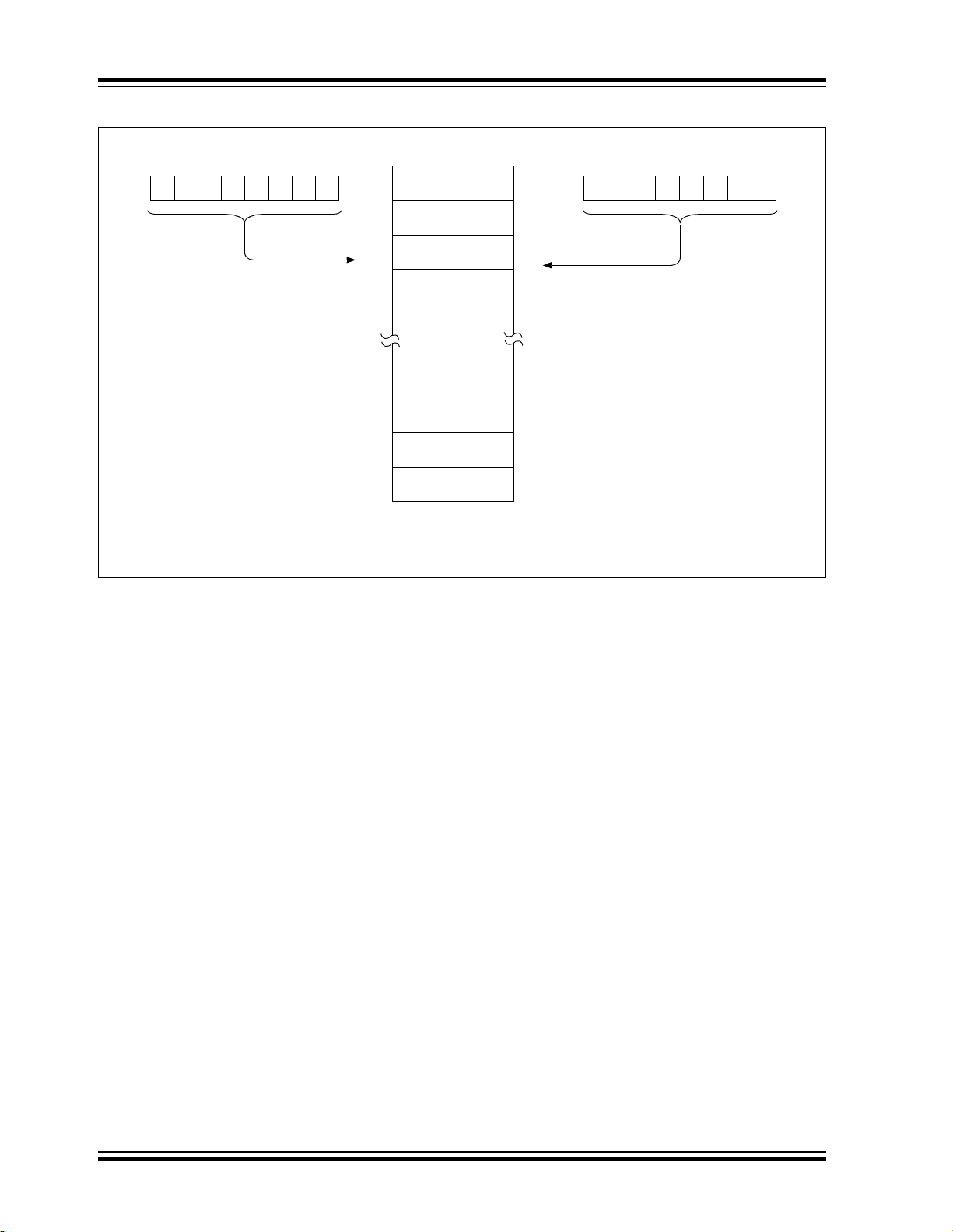
PIC18F2XK20/4XK20
Note 1: The Access RAM bit of the instruction can be used to force an override of the selected bank (BSR<3:0>) to
the registers of the Access Bank.
2: The MOVFF instruction embeds the entire 12-bit address in the instruction.
Data
Memory
Bank Select
(2)
7
0
From Opcode
(2)
0000
000h
100h
200h
300h
F00h
E00h
FFFh
Bank 0
Bank 1
Bank 2
Bank 14
Bank 15
00h
FFh
00h
FFh
00h
FFh
00h
FFh
00h
FFh
00h
FFh
Bank 3
through
Bank 13
0011
11111111
7
0
BSR
(1)
FIGURE 5-9: USE OF THE BANK SELECT REGISTER (DIRECT ADDRESSING)
DS41303G-page 76 2010 Microchip Technology Inc.

PIC18F2XK20/4XK20
5.3.2 ACCESS BANK
While the us e of the BSR w ith an em bedded 8-b it
address a llows users to ad dress th e e ntire range of
data memory, it also means that the user must always
ensure th at th e co rrect ban k i s s elected. O therwise,
data may be read from or written to the wrong location.
This can be disastrous if a GPR is the intended target
of an op eration, b ut a n SF R is w ritten to i nstead.
Verifying an d/or ch anging the BSR for ea ch read or
write to data memory can become very inefficient.
To streamline access for the most commonly used data
memory locations, the data memory is configured with
an Access Bank , w hich all ows us ers to access a
mapped block of me mory without sp ecifying a BSR.
The Access Bank consists of the first 96 bytes of memory (00h-5Fh) in Bank 0 and the last 160 bytes of memory (60h-FFh) in Block 15. The lower half is known as
the “Ac cess RAM” an d is co mposed of GPRs. Thi s
upper hal f is al so w here the dev ice’s SFR s a re
mapped. These two areas are mapped contiguously in
the Ac cess Ba nk and ca n b e a ddressed in a l inear
fashion by an 8-bit address (Figures 5-5 through 5-7).
The Access Bank is used by core PIC18 instructions
that include the Access RAM bit (the ‘a’ parameter in
the instruction). When ‘a’ is equal to ‘1’, the instruction
uses the BSR a nd th e 8 -bit a ddress i ncluded in th e
opcode for the data memory address. When ‘a’ is ‘0’,
however, th e in struction i s f orced t o us e t he A ccess
Bank add ress m ap; the cu rrent va lue of th e BSR i s
ignored entirely.
Using this “forced” addressing allows the instruction to
operate o n a da ta address in a s ingle cycle, without
updating the BSR first. For 8-bit addresses of 60h and
above, this means that users can evaluate and operate
on SFRs more efficiently. The Access RAM below 60h
is a good place for data values that the user might need
to ac cess ra pidly, s uch a s immediate c omputational
results or co mmon pr ogram variables. Access RAM
also allows for f aster and more code efficient context
saving and switching of variables.
The mapping of the Access Bank is slightly different
when the extended instruction set is enabled (XINST
Configuration bit = 1). This is discussed in more detail
in Section 5.5.3 “Mapping the Access Bank in
Indexed Literal Offset Mode”.
5.3.3 GENERAL PURPOSE REGISTER FILE
PIC18 devices may have banked memory in the G PR
area. This is data RAM, which is available for use by all
instructions. G PRs st art at the bottom of B ank 0
(address 000h) and grow upwards towards the bottom of
the SFR area. GPR s are not initialized by a P ower-on
Reset and are unchanged on all other Resets.
5.3.4 SPECIAL FUNCTION REGISTERS
The S pecial Function Registers (SFRs) are re gisters
used by the CPU and peripheral modules for controlling
the desired operation of the device. These registers are
implemented as s tatic RAM. SFRs start at the top of
data memory (FFFh) and extend downward to occupy
the t op portion of Bank 1 5 (F 60h to FFFh). A list of
these registers is given in Table 5-1 and Table 5-2.
The SFRs c an b e classified i nto t wo sets: th ose
associated w ith the “c ore” de vice functionality (ALU ,
Resets a nd in terrupts) a nd those related to th e
peripheral functions. The Reset and interrupt registers
are des cribed in their res pective c hapters, w hile th e
ALU’s ST ATUS re gister is de scribed later i n this
section. R egisters rela ted to the ope ration o f a
peripheral feature are described in the chapter for that
peripheral.
The SF Rs a re ty pically d istributed am ong th e
peripherals whose functions they control. Unused SFR
locations are unimplemented and read as ‘0’s.
2010 Microchip Technology Inc. DS41303G-page 77

PIC18F2XK20/4XK20
TABLE 5-1: SPECIAL FUNCTION REGISTER MAP FOR PIC18F2XK20/4XK20 DEVICES
Address Name Address Name Address Name Address Name
FFFh TOSU FD7h TMR0H FAFh SPBRG F87h
FFEh TOSH FD6h TMR0L FAEh RCREG F86h —
FFDh TOSL FD5h T0CON FADh TXREG F85h —
FFCh STKPTR FD4h —
FFBh PCLATU FD3h OSCCON FABh RCSTA F83h PORTD
FFAh PCLATH FD2h HLVDCON FAAh EEADRH
FF9h PCL FD1h WDTCON FA9h EEADR F81h PORTB
FF8h TBLPTRU FD0h RCON FA8h EEDATA F80h PORTA
FF7h TBLPTRH FCFh TMR1H FA7h EECON2
FF6h TBLPTRL FCEh TMR1L FA6h EECON1 F7Eh ANSEL
FF5h TABLAT FCDh T1CON FA5h —
FF4h PRODH FCCh TMR2 FA4h
FF3h PRODL FCBh PR2 FA3h
FF2h INTCON FCAh T2CON FA2h IPR2 F7Ah CM2CON0
FF1h INTCON2 FC9h SSPBUF FA1h PIR2 F79h CM2CON1
FF0h INTCON3 FC8h SSPADD FA0h PIE2 F78h SLRCON
(1)
FEFh INDF0
FEEh POSTINC0
FEDh POSTDEC0
FECh PREINC0
FEBh PLUSW0
F C7h SSPSTAT F9Fh IPR1 F77h SSPMSK
(1)
(1)
(1)
(1)
FC6h SSPCON1 F9Eh PIR1 F76h —
FC5h SSPCON2 F9Dh PIE1 F75h —
FC4h ADRESH F9Ch —
FC3h ADRESL F9Bh OSCTUNE F73h —
FEAh FSR0H FC2h ADCON0 F9Ah —
FE9h FSR0L FC1h ADCON1 F99h —
FE8h WREG FC0h ADCON2 F98h —
FE7h INDF1
FE6h POSTINC1
FE5h POSTDEC1
FE4h PREINC1
FE3h PLUSW1
(1)
(1)
(1)
(1)
(1)
FBFh CCPR1H F97h —
FBEh CCPR1L F96h TRISE
FBDh CCP1CON F95h TRISD
FBCh CCPR2H F94h TRISC F6Ch —
FBBh CCPR2L F93h TRISB F6Bh —
FE2h FSR1H FBAh CCP2CON F92h TRISA F6Ah —
FE1h FSR1L FB9h PSTRCON F91h —
FE0h BSR FB8h BAUDCON F90h —
FDFh INDF2
FDEh POSTINC2
FDDh POSTDEC2
FDCh PREINC2
FDBh PLUSW2
(1)
F B7h PWM1CON F8Fh —
(1)
(1)
(1)
(1)
FB6h ECCP1AS F8Eh —
FB5h CVRCON F8Dh LATE
FB4h CVRCON2 F8Ch LATD
FB3h TMR3H F8Bh LATC F63h —
FDAh FSR2H FB2h TMR3L F8Ah LATB F62h —
FD9h FSR2L FB1h T3CON F89h LATA F61h —
FD8h STATUS FB0h SPBRGH F88h —
(2)
FACh TXSTA F84h PORTE
(4)
(1)
(2)
(2)
—
(2)
—
(2)
(2)
(2)
(2)
(2)
(3)
(3)
(2)
(2)
(2)
(2)
(3)
F65 h —
(3)
F64 h —
(2)
F82h PORTC
F7Fh ANSELH
F7Dh IOCB
F7Ch WPUB
F7Bh CM1CON0
F74h —
F72h —
F71h —
F70h —
F6Fh —
F6Eh —
F6Dh —
F69h —
F68h —
F67h —
F66h —
F60h —
—
(2)
(2)
(2)
(2)
(2)
(2)
(2)
(2)
(2)
(2)
(2)
(2)
(2)
(2)
(2)
(2)
(2)
(2)
(2)
(2)
(2)
(2)
(2)
(2)
(2)
(2)
(3)
Note 1: This is not a physical register.
2: Unimplemented registers are read as ‘0’.
3: This register is not available on PIC18F2XK20 devices.
4: This register is only implemented in the PIC18F46K20 and PIC18F26K20 devices.
DS41303G-page 78 2010 Microchip Technology Inc.

PIC18F2XK20/4XK20
TABLE 5-2: REGISTER FILE SUMMARY (PIC18F2XK20/4XK20)
File Name Bit 7 Bit 6 Bit 5 Bit 4 Bit 3 Bit 2 Bit 1 Bit 0
TOSU
TOSH Top-of-Stack, High Byte (TOS<15:8>) 0000 0000 59, 66
TOSL Top-of-Stack, Low Byte (TOS<7:0>) 0000 0000 59, 66
STKPTR STKFUL STKUNF
PCLATU
PCLATH Holding Register for PC<15:8> 0000 0000 59, 66
PCL PC, Low Byte (PC<7:0>) 0000 0000 59, 66
TBLPTRU
TBLPTRH Program Memory Table Pointer, High Byte (TBLPTR<15:8>) 0000 0000 59, 92
TBLPTRL Program Memory Table Pointer, Low Byte (TBLPTR<7:0>) 0000 0000 59, 92
TABLAT Program Memory Table Latch 0000 0000 59, 92
PRODH Product Register, High Byte xxxx xxxx 59, 105
PRODL Product Register, Low Byte xxxx xxxx 59, 105
INTCON GIE/GIEH PEIE/GIEL TMR0IE INT0IE RBIE TMR0IF INT0IF RBIF 0000 000x 59, 109
INTCON2 RBPU
INTCON3 INT2IP INT1IP
INDF0 Uses contents of FSR0 to address data memory – value of FSR0 not changed (not a physical register) N/A 59, 84
POSTINC0 Uses contents of FSR0 to address data memory – value of FSR0 post-incremented (not a physical register) N/A 59, 84
POSTDEC0 Uses contents of FSR0 to address data memory – value of FSR0 post-decremented (not a physical register) N/A 59, 84
PREINC0 Uses contents of FSR0 to address data memory – value of FSR0 pre-incremented (not a physical register) N/A 59, 84
PLUSW0 Uses contents of FSR0 to address data memory – value of FSR0 offset by W (not a physical register) – N/A 59, 84
FSR0H
FSR0L Indirect Data Memory Address Pointer 0, Low Byte xxxx xxxx 59, 84
WREG Working Register xxxx xxxx 59
INDF1 Uses contents of FSR1 to address data memory – value of FSR1 not changed (not a physical register) N/A 59, 84
POSTINC1 Uses contents of FSR1 to address data memory – value of FSR1 post-incremented (not a physical register) N/A 59, 84
POSTDEC1 Uses contents of FSR1 to address data memory – value of FSR1 post-decremented (not a physical register) N/A 59, 84
PREINC1 Uses contents of FSR1 to address data memory – value of FSR1 pre-incremented (not a physical register) N/A 59, 84
PLUSW1 Uses contents of FSR1 to address data memory – value of FSR1 offset by W (not a physical register) – value of N/A 59, 84
FSR1H
FSR1L Indirect Data Memory Address Pointer 1, Low Byte xxxx xxxx 60, 84
BSR
INDF2 Uses contents of FSR2 to address data memory – value of FSR2 not changed (not a physical register) N/A 60, 84
POSTINC2 Uses contents of FSR2 to address data memory – value of FSR2 post-incremented (not a physical register) N/A 60, 84
POSTDEC2 Uses contents of FSR2 to address data memory – value of FSR2 post-decremented (not a physical register) N/A 60, 84
PREINC2 Uses contents of FSR2 to address data memory – value of FSR2 pre-incremented (not a physical register) N/A 60, 84
PLUSW2 Uses contents of FSR2 to address data memory – value of FSR2 offset by W (not a physical register) – value of N/A 60, 84
FSR2H
FSR2L Indirect Data Memory Address Pointer 2, Low Byte xxxx xxxx 60, 84
STATUS
Legend: x = unknown, u = unchanged, — = unimplemented, q = value depends on condition
Note 1: The SBOREN bit is only available when the BOREN<1:0> Configuration bits = 01; otherwise it is disabled and reads as ‘0’. See
2: These registers and/or bits are not implemented on 28-pin devices and are read as ‘0’. Reset values are shown for 40/44-pin devices;
3: The PLLEN bit is only available in specific oscillator configuration; otherwise it is disabled and reads as ‘0’. See Section 2.6.2 “PLL in
4: The RE3 bit is only available when Master Clear Reset is disabled (MCLRE Configuration bit = 0). Otherwise, RE3 reads as ‘0’. This bit is
5: RA6/RA7 and their associated latch and direction bits are individually configured as port pins based on various primary oscillator modes.
6: All bits of the ANSELH register initialize to ‘0’ if the PBADEN bit of CONFIG3H is ‘0’.
7: This register is only implemented in the PIC18F46K20 and PIC18F26K20 devices.
— — — Top-of-Stack Upper Byte (TOS<20:16>) ---0 0000 59, 66
— SP4 SP3 SP2 SP1 SP0 00-0 0000 59, 67
— — — Holding Register for PC<20:16> ---0 0000 59, 66
— — bit 21 Program Memory Table Pointer Upper Byte (TBLPTR<20:16>) --00 0000 59, 92
INTEDG0 INTEDG1 INTEDG2 —TMR0IP—RBIP1111 -1-1 59, 110
—INT2IEINT1IE— INT2IF INT1IF 11-0 0-00 59 , 111
— — — — Indirect Data Memory Address Pointer 0, High Byte ---- 0000 59, 84
— — — — Indirect Data Memory Address Pointer 1, High Byte ---- 0000 60, 84
— — — — Bank Select Register ---- 0000 60, 71
— — — — Indirect Data Memory Address Pointer 2, High Byte ---- 0000 60, 84
— — —NOVZDCC---x xxxx 60, 82
Section 4.4 “Brown-out Reset (BOR)”.
individual unimplemented bits should be interpreted as ‘-’.
HFINTOSC Modes”.
read-only.
When disabled, these bits read as ‘0’.
Value on
POR, BOR
Details
on page:
2010 Microchip Technology Inc. DS41303G-page 79

PIC18F2XK20/4XK20
TABLE 5-2: REGISTER FILE SUMMARY (PIC18F2XK20/4XK20) (CONTINUED)
File Name Bit 7 Bit 6 Bit 5 Bit 4 Bit 3 Bit 2 Bit 1 Bit 0
TMR0H Timer0 Register, High Byte 0000 0000 60, 157
TMR0L Timer0 Register, Low Byte xxxx xxxx 60, 157
T0CON TMR0ON T08BIT T0CS T0SE PSA T0PS2 T0PS1 T0PS0 1111 1111 60, 155
OSCCON IDLEN IRCF2 IRCF1 IRCF0 OSTS IOFS SCS1 SCS0 0011 qq00 29, 60
HLVDCON VDIRMAG
WDTCON
RCON IPEN SBOREN
TMR1H Timer1 Register, High Byte xxxx xxxx 60, 165
TMR1L Timer1 Register, Low Bytes xxxx xxxx 60, 165
T1CON RD16 T1RUN T1CKPS1 T1CKPS0 T1OSCEN T1SYNC
TMR2 Timer2 Register 0000 0000 60, 168
PR2 Timer2 Period Register 1111 1111 60, 168
T2CON
SSPBUF SSP Receive Buffer/Transmit Register xxxx xxxx 60, 201,
SSPADD SSP Address Register in I
SSPSTAT SMP CKE D/A
SSPCON1 WCOL SSPOV SSPEN CKP SSPM3 SSPM2 SSPM1 SSPM0 0000 0000 60, 195,
SSPCON2 GCEN ACKSTAT ACKDT ACKEN RCEN PEN RSEN SEN 0000 0000 60, 206
ADRESH A/D Result Register, High Byte xxxx xxxx 61, 277
ADRESL A/D Result Register, Low Byte xxxx xxxx 61, 277
ADCON0
ADCON1
ADCON2 ADFM
CCPR1H Capture/Compare/PWM Register 1, High Byte xxxx xxxx 61, 144
CCPR1L Capture/Compare/PWM Register 1, Low Byte xxxx xxxx 61, 144
CCP1CON P1 M1 P1M0 DC1B1 DC1B0 CCP1M3 CCP1M2 CCP1M1 CCP1M0 0000 0000 61, 173
CCPR2H Capture/Compare/PWM Register 2, High Byte xxxx xxxx 61, 144
CCPR2L Capture/Compare/PWM Register 2, Low Byte xxxx xxxx 61, 144
CCP2CON
PSTRCON
BAUDCON ABDOVF RCIDL DTRXP CKTXP BRG16
PWM1CON PRSEN PDC6 PDC5 PDC4 PDC3 PDC2 PDC1 PDC0 0000 0000 61, 186
ECCP1AS ECCPASE ECCPAS2 ECCPAS1 ECCPAS0 PSSAC1 PSSAC0 PSSBD1 PSSBD0 0000 0000 61, 183
CVRCON CVREN CVROE CVRR CVRSS CVR3 CVR2 CVR1 CVR0 0000 0000 61, 291
CVRCON2 FVREN FVRST
TMR3H Timer3 Register, High Byte xxxx xxxx 61, 172
TMR3L Timer3 Register, Low Byte xxxx xxxx 61, 172
T3CON RD16 T3CCP2 T3CKPS1 T3CKPS0 T3CCP1 T3SYNC
Legend: x = unknown, u = unchanged, — = unimplemented, q = value depends on condition
Note 1: The SBOREN bit is only available when the BOREN<1:0> Configuration bits = 01; otherwise it is disabled and reads as ‘0’. See
2: These registers and/or bits are not implemented on 28-pin devices and are read as ‘0’. Reset values are shown for 40/44-pin devices;
3: The PLLEN bit is only available in specific oscillator configuration; otherwise it is disabled and reads as ‘0’. See Section 2.6.2 “PLL in
4: The RE3 bit is only available when Master Clear Reset is disabled (MCLRE Configuration bit = 0). Otherwise, RE3 reads as ‘0’. This bit is
5: RA6/RA7 and their associated latch and direction bits are individually configured as port pins based on various primary oscillator modes.
6: All bits of the ANSELH register initialize to ‘0’ if the PBADEN bit of CONFIG3H is ‘0’.
7: This register is only implemented in the PIC18F46K20 and PIC18F26K20 devices.
— — — — — — —SWDTEN--- ---0 60, 309
— T2OUTPS3 T2OUTPS2 T2OUTPS1 T2OUTPS0 TMR2ON T2CKPS1 T2CKPS0 -000 0000 60, 167
— — CHS3 CHS2 CHS1 CHS0 GO/DONE ADON --00 0000 61, 271
— —VCFG1VCFG0— — — — --00 ---- 59, 272
— — DC2B1 DC2B0 CCP2M3 CCP2M2 CCP2M1 CCP2M0 --00 0000 61, 143
— — — STRSYNC STRD STRC STRB STRA ---0 0001 61, 187
Section 4.4 “Brown-out Reset (BOR)”.
individual unimplemented bits should be interpreted as ‘-’.
HFINTOSC Modes”.
read-only.
When disabled, these bits read as ‘0’.
— IRVST HLVDEN HLVDL3 HLVDL2 HLVDL1 HLVDL0 0-00 0101 60, 293
(1)
—RITO PD POR BOR 0q-1 11q0 51, 58,
TMR1CS TMR1ON 0000 0000 60, 159
2
C™ Slave Mode. SSP Baud Rate Reload Register in I2C Master Mode. 0000 0000 60, 202
PSR/WUA BF 0000 0000 60, 194,
— ACQT2 ACQT1 ACQT0 ADCS2 ADCS1 ADCS0 0-00 0000 61, 273
— WUE ABDEN 0100 0-00 61, 248
— — — — — — 00-- ---- 61, 292
TMR3CS TMR3ON 0000 0000 61, 169
Value on
POR, BOR
Details
on page:
118
202
204
205
DS41303G-page 80 2010 Microchip Technology Inc.

PIC18F2XK20/4XK20
TABLE 5-2: REGISTER FILE SUMMARY (PIC18F2XK20/4XK20) (CONTINUED)
File Name Bit 7 Bit 6 Bit 5 Bit 4 Bit 3 Bit 2 Bit 1 Bit 0
Value on
POR, BOR
SPBRGH EUSART Baud Rate Generator Register, High Byte 0000 0000 61, 241
SPBRG EUSART Baud Rate Generator Register, Low Byte 0000 0000 61, 241
RCREG EUSART Receive Register 0000 0000 61, 238
TXREG EUSART Transmit Register 0000 0000 61, 237
TXSTA CSRC TX9 TXEN SYNC SENDB BRGH TRMT TX9D 0000 0010 61, 246
RCSTA SPEN RX9 SREN CREN ADDEN FERR OERR RX9D 0000 000x 61, 247
EEADR EEADR7 EEADR6 EEADR5 EEADR4 EEADR3 EEADR2 EEADR1 EEADR0 0000 0000 61, 90, 99
(7)
EEADRH
— — — — — — EEADR9 EEADR8 ---- --00 61, 90, 99
EEDATA EEPROM Data Register 0000 0000 61, 90, 99
EECON2 EEPROM Control Register 2 (not a physical register) 0000 0000 61, 90, 99
EECON1 EEPGD CFGS
— FREE WRERR WREN WR RD xx-0 x000 61, 91, 99
IPR2 OSCFIP C1IP C2IP EEIP BCLIP HLVDIP TMR3IP CCP2IP 1111 1111 62, 117
PIR2 OSCFIF C1IF C2IF EEIF BCLIF HLVDIF TMR3IF CCP2IF 0000 0000 62, 113
PIE2 OSCFIE C1IE C2IE EEIE BCLIE HLVDIE TMR3IE CCP2IE 0000 0000 62, 115
IPR1 PSPIP
PIR1 PSPIF
PIE1 PSPIE
OSCTUNE INTSRC PLLEN
(2)
TRISE
(2)
TRISD
(2)
ADIP RCIP TXIP SSPIP CCP1IP TMR2IP TMR1IP 1111 1111 62, 116
(2)
ADIF RCIF TXIF SSPIF CCP1IF TMR2IF TMR1IF 0000 0000 62, 112
(2)
ADIE RCIE TXIE SSPIE CCP1IE TMR2IE TMR1IE 0000 0000 62, 114
(3)
TUN5 TUN4 TUN3 TUN2 TUN1 TUN0 0q00 0000 33, 62
IBF OBF IBOV PSPMODE — TRISE2 TRISE1 TRISE0 0000 -111 62, 134
PORTD Data Direction Control Register 1111 1111 62, 130
TRISC PORTC Data Direction Control Register 1111 1111 62, 127
TRISB PORTB Data Direction Control Register 1111 1111 62, 124
TRISA TRISA7
(2)
LATE
LATD
(2)
— — — — — PORTE Data Latch Register
PORTD Data Latch Register (Read and Write to Data Latch) xxxx xxxx 62, 130
(5)
TRISA6
(5)
Data Direction Control Register for PORTA 1111 1111 62, 121
(Read and Write to Data Latch)
---- -xxx 62, 133
LATC PORTC Data Latch Register (Read and Write to Data Latch) xxxx xxxx 62, 127
LATB PORTB Data Latch Register (Read and Write to Data Latch) xxxx xxxx 62, 124
LATA LATA7
PORTE
PORTD
(2)
— — — —RE3
RD7 RD6 RD5 RD4 RD3 RD2 RD1 RD0 xxxx xxxx 62, 130
(5)
LATA6
(5)
PORTA Data Latch Register (Read and Write to Data Latch) xxxx xxxx 62, 121
(4)
RE2
(2)
RE1
(2)
RE0
(2)
---- x000 62, 133
PORTC RC7 RC6 RC5 RC4 RC3 RC2 RC1 RC0 xxxx xxxx 62, 127
PORTB RB7 RB6 RB5 RB4 RB3 RB2 RB1 RB0 xxx0 0000 62, 124
PORTA RA7
(6)
ANSELH
ANSEL ANS7
(5)
— — — ANS12 ANS11 ANS10 ANS9 ANS8 ---1 1111 62, 137
(2)
IOCB IOCB7 IOCB6 IOCB5 IOCB4
RA6
ANS6
(5)
(2)
RA5 RA4 RA3 RA2 RA1 RA0 xx0x 0000 62, 121
(2)
ANS5
ANS4 ANS3 ANS2 ANS1 ANS0 1111 1111 62, 136
— — — — 0000 ---- 62, 124
WPUB WPUB7 WPUB6 WPUB5 WPUB4 WPUB3 WPUB2 WPUB1 WPUB0 1111 1111 62, 124
CM1CON0 C1ON C1OUT C1OE C1POL C1SP C1R C1CH1 C1CH0 0000 0000 62, 284
CM2CON0 C2ON C2OUT C2OE C2POL C2SP C2R C2CH1 C2CH0 0000 0000 62, 285
CM2CON1 MC1OUT MC2OUT C1RSEL C2RSEL
SLRCON
— — —SLRE
(2)
— — — — 0000 ---- 63, 287
(2)
SLRD
SLRC SLRB SLRA ---1 1111 63, 138
SSPMSK MSK7 MSK6 MSK5 MSK4 MSK3 MSK2 MSK1 MSK0 1111 1111 63, 213
Legend: x = unknown, u = unchanged, — = unimplemented, q = value depends on condition
Note 1: The SBOREN bit is only available when the BOREN<1:0> Configuration bits = 01; otherwise it is disabled and reads as ‘0’. See
Section 4.4 “Brown-out Reset (BOR)”.
2: These registers and/or bits are not implemented on 28-pin devices and are read as ‘0’. Reset values are shown for 40/44-pin devices;
individual unimplemented bits should be interpreted as ‘-’.
3: The PLLEN bit is only available in specific oscillator configuration; otherwise it is disabled and reads as ‘0’. See Section 2.6.2 “PLL in
HFINTOSC Modes”.
4: The RE3 bit is only available when Master Clear Reset is disabled (MCLRE Configuration bit = 0). Otherwise, RE3 reads as ‘0’. This bit is
read-only.
5: RA6/RA7 and their associated latch and direction bits are individually configured as port pins based on various primary oscillator modes.
When disabled, these bits read as ‘0’.
6: All bits of the ANSELH register initialize to ‘0’ if the PBADEN bit of CONFIG3H is ‘0’.
7: This register is only implemented in the PIC18F46K20 and PIC18F26K20 devices.
Details
on page:
2010 Microchip Technology Inc. DS41303G-page 81

PIC18F2XK20/4XK20
5.3.5 STATUS REGISTER
The STATUS register, shown in Register 5-2, contains
the arithmetic status of the ALU. As with any other SFR,
it can be the operand for any instruction.
If the STATUS register is the destination for an instruction that affects the Z, DC, C, OV or N bits, the results
of the instruction are not written; instead, the STATUS
register is u pdated according to th e ins truction p erformed. Therefore, the result of an instruction with the
STATUS re gister as it s d estination may b e d ifferent
than intended. As an example, CLRF STATUS will set
the Z bit and le ave the rem aining S tatus bit s
unchanged (‘000u u1uu’).
It is recommended that only BCF, BSF, SWAPF, MOVFF
and MOVWF instructions are used to alter the STATUS
register, because these instructions do not affect the Z,
C, DC, OV or N bits in the STATUS register.
For other instructions that do not affect Status bits, see
the ins truction s et s ummaries in T able 24-2 an d
Table 24-3.
Note: The C and DC bits operate as the borrow
and di git borrow bits, res pectively, in
subtraction.
REGISTER 5-2: STATUS: STATUS REGISTER
U-0 U-0 U-0 R/W-x R/W-x R/W-x R/W-x R/W-x
— — —
bit 7 bit 0
Legend:
R = Readable bit W = Writable bit U = Unimplemented bit, read as ‘0’
-n = Value at POR ‘1’ = Bit is set ‘0’ = Bit is cleared x = Bit is unknown
NOV Z DC
(1)
(1)
C
bit 7-5 Unimplemented: Read as ‘0’
bit 4 N: Negative bit
This bit is used for signed arithmetic (two’s complement). It indicates whether the result was negative
(ALU MSB = 1).
1 = Result was negative
0 = Result was positive
bit 3 OV: Overflow bit
This bit is used for signed arithmetic (two’s complement). It indicates an overflow of the 7-bit magnitude which causes the sign bit (bit 7 of the result) to change state.
1 = Overflow occurred for signed arithmetic (in this arithmetic operation)
0 = No overflow occurred
bit 2 Z: Zero bit
1 = The result of an arithmetic or logic operation is zero
0 = The result of an arithmetic or logic operation is not zero
bit 1 DC: Digit Carry/Borrow
1 = A carry-out from the 4th low-order bit of the result occurred
0 = No carry-out from the 4th low-order bit of the result
bit 0 C: Carry/Borrow
1 = A carry-out from the Most Significant bit of the result occurred
0 = No carry-out from the Most Significant bit of the result occurred
Note 1: For Borrow
second operand. For rotate (RRF, RLF) instructions, this bit is loaded with either the high-order or low-order
bit of the source register.
, the polarity is reversed. A subtraction is executed by adding the two’s complement of the
bit (ADDWF, ADDLW,SUBLW,SUBWF instructions)
bit (ADDWF, ADDLW, SUBLW, SUBWF instructions)
(1)
(1)
DS41303G-page 82 2010 Microchip Technology Inc.

PIC18F2XK20/4XK20
LFSR FSR0, 100h ;
NEXT CLRF POSTINC0 ; Clear INDF
; register then
; inc pointer
BTFSS FSR0H, 1 ; All done with
; Bank1?
BRA NEXT ; NO, clear next
CONTINUE ; YES, continue
5.4 Data Addressing Modes
Note: The execution of so me instruc tions in the
core P IC18 i nstruction set are c hanged
when the PIC18 extended instruction set is
enabled. See Section 5.5 “Data Memory
and the Extended Instruction Set” for
more information.
While the program memory can be addressed in only
one way – through the program counter – information
in the data memory space can be addressed in several
ways. Fo r mo st ins tructions, the a ddressing mode i s
fixed. Other instructions may u se up to three modes,
depending on which operands are used and whether or
not the extended instruction set is enabled.
The addressing modes are:
• Inherent
• Literal
•Direct
•Indirect
An additional addressing mode, Indexed Literal Offset,
is a vailable w hen the ext ended i nstruction s et i s
enabled (XINST Configuration bit = 1). Its operation is
discussed in greater detail in Section 5.5.1 “Indexed
Addressing with Literal Offset”.
5.4.1 INHERENT AND LITERAL ADDRESSING
Many PIC18 control instructions do not need any argument at all; they either perform an operation that globally affects the device or they operate implicitly on one
register. This addressing mode is known as Inherent
Addressing. Examples include SLEEP, RESET and DAW.
Other instructions work in a similar way but require an
additional explicit argument in th e opc ode. Th is i s
known as Li teral Add ressing mo de b ecause the y
require some literal value as an argument. Examples
include ADDLW and MOVLW, which respectively, add or
move a literal value to the W register. Other examples
include CALL an d GOTO, w hich i nclude a 20-bit
program memory address.
The Access RAM bit ‘a’ determines how the address is
interpreted. Wh en ‘a ’ is ‘1’, th e co ntents of the BSR
(Section 5.3.1 “Bank Select Register (BSR)”) a re
used with the address to determine the complete 12-bit
address of the register. When ‘a’ is ‘0’, the address is
interpreted a s being a register i n t he Access Bank.
Addressing tha t uses the Acc ess R AM is sometimes
also known as Direct Forced Addressing mode.
A few instructions, such as MOVFF, include the entire
12-bit ad dress (either s ource or de stination) in the ir
opcodes. In these cases, the BSR is ignored entirely.
The destination of the operation’s results is determined
by the destination bit ‘d’. When ‘d’ is ‘1’, the results are
stored back in the source register, overwriting its original contents. When ‘d’ is ‘0’, the results are stored in
the W reg ister. Instructions with out the ‘d ’ a rgument
have a destination that is implicit in the instruction; their
destination is either the target register being operated
on or the W register.
5.4.3 INDIRECT ADDRESSING
Indirect addressing allows the user to access a location
in data memory without giving a f ixed address in the
instruction. This is done by using File Select Registers
(FSRs) as pointers to the locations which are to be read
or written. Since the FSRs are themselves located in
RAM as Special F ile R egisters, th ey ca n al so be
directly manipulated un der pro gram co ntrol. Thi s
makes FSR s ve ry useful in implementing data structures, such as tables and arrays in data memory.
The re gisters fo r in direct add ressing are a lso
implemented with Indirect File Operands (INDFs) that
permit automatic manipulation of the pointer value with
auto-incrementing, au to-decrementing o r of fsetting
with another value. This allows for efficient code, using
loops, such as the example of clearing an entire RAM
bank in Example 5-5.
EXAMPLE 5-5: HOW TO CLEAR RAM
(BANK 1) USING
INDIRECT ADDRESSING
5.4.2 DIRECT ADDRESSING
Direct ad dressing sp ecifies all or part of the so urce
and/or destination address of the operation within the
opcode it self. The o ptions a re specified by th e
arguments accompanying the instruction.
In the core PIC18 instruction set, bit-oriented and byteoriented ins tructions us e s ome v ersion of d irect
addressing by default. All of these instructions include
some 8 -bit literal add ress a s t heir Lea st Sign ificant
Byte. This address specifies either a register address in
one of the banks of data RAM (Sectio n 5.3.3 “General
Purpose Register File”) or a loc ation in the Access
Bank ( Section 5.3.2 “Access Bank”) as the da ta
source for the instruction.
2010 Microchip Technology Inc. DS41303G-page 83

PIC18F2XK20/4XK20
FSR1H:FSR1L
0
7
Data Memory
000h
100h
200h
300h
F00h
E00h
FFFh
Bank 0
Bank 1
Bank 2
Bank 14
Bank 15
Bank 3
through
Bank 13
ADDWF, INDF1, 1
07
Using an instruction with one of the
indirect addressing registers as the
operand....
...uses the 12-bit address stored in
the F SR p air assoc iated wit h that
register....
...to det ermine t he data mem ory
location to be used in that operation.
In this case, the FSR1 pair contains
ECCh. This means the contents of
location ECCh will be added to that
of the W register and stored back in
ECCh.
xxxx1110 11001100
5.4.3.1 FSR Registers and the INDF
Operand
At the core of indirect addressing are three sets of registers: FSR0, FSR1 and FSR2. Each represents a pair
of 8-bit registers, FSRnH and FSRnL. Each FSR pair
holds a 12-bit value, therefore the four upper bits of the
FSRnH register are not used. The 12-bit FSR value can
address the entire range of the data memory in a linear
fashion. The FSR register pairs, then, serve as pointers
to data memory locations.
Indirect addressing is ac complished w ith a s et of
Indirect File Operands, INDF0 through INDF2. These
can be tho ught o f a s “virtual” re gisters: they a re
mapped in th e SFR sp ace but are no t phy sically
implemented. R eading or w riting to a particular INDF
register actually a ccesses it s co rresponding FSR
register pair. A read from INDF1, for ex ample, reads
the data at th e add ress in dicated by FSR1H:FSR1L.
Instructions that use the IN DF registers as o perands
actually use the contents of their corresponding FSR as
a pointer to the instruction’s target. The INDF operand
is just a convenient way of using the pointer.
Because indirect addressing uses a full 12-bit address,
data RAM banking is not necessary. Thus, the current
contents of the BSR and the Access RAM bit have no
effect on determining the target address.
5.4.3.2 FSR Registers and POSTINC,
POSTDEC, PREINC and PLUSW
In addition to the INDF operand, each FSR register pair
also has four additional indirect operands. Like INDF,
these a re “virtual” re gisters which cannot b e d irectly
read o r written. Ac cessing thes e re gisters ac tually
accesses the loc ation to w hich th e as sociated FSR
register pair points, and also performs a specific action
on the FSR value. They are:
• POSTDEC: accesses the location to which the
FSR points, then automatically decrements the
FSR by 1 afterwards
• POSTINC: accesses the location to which the
FSR points, then automatically increments the
FSR by 1 afterwards
• PREINC: automatically increments the FSR by 1,
then uses the location to which the FSR points in
the operation
• PLUSW: adds the signed value of the W register
(range of -127 to 128) to that of the FSR and uses
the location to which the result points in the
operation.
In thi s c ontext, ac cessing an IN DF reg ister uses the
value in the associated FSR register without changing
it. S imilarly, accessing a PLUSW r egister g ives t he
FSR value an offset by that in the W register; however,
neither W no r the FSR is act ually changed in th e
operation. Ac cessing th e o ther vi rtual re gisters
changes the value of the FSR register.
FIGURE 5-10: INDIRECT ADDRESSING
DS41303G-page 84 2010 Microchip Technology Inc.

PIC18F2XK20/4XK20
Operations on the F SRs w ith PO STDEC, PO STINC
and PREINC affect the entire register pair; that is, rollovers of the FSRnL register from FFh to 00h carry over
to the FSR nH register. O n the oth er hand, results of
these operations do not change the value of any flags
in the STATUS register (e.g., Z, N, OV, etc.).
The PLUSW register can be used to implement a form
of indexed addressing in the data memory space. By
manipulating the v alue i n the W regi ster, us ers ca n
reach ad dresses tha t are fix ed of fsets from po inter
addresses. In so me applications, this can be used to
implement s ome powerful pro gram control s tructure,
such as software stacks, inside of data memory.
5.4.3.3 Operations by FSRs on FSRs
Indirect addressing operations that target other FSRs
or virtual r egisters r epresent s pecial cases. For
example, using a n FSR to point to one of the virtual
registers will not result in successful operations. As a
specific case, as sume that FSR 0H:FSR0L c ontains
FE7h, the address o f IN DF1. Atte mpts t o rea d th e
value of the IN DF1 u sing INDF0 as a n o perand w ill
return 00h. Attempts to write to INDF1 using INDF0 as
the operand will result in a NOP.
On the other hand, using the virtual registers to write to
an FSR pair may not occur as planned. In these cases,
the value will be written to the FSR pair but without any
incrementing or decrementing. Thus, w riting to either
the INDF2 or POSTDEC2 register will write the same
value to the FSR2H:FSR2L.
Since the FSRs are physical registers mapped in the
SFR space, they can be manipulated through all direct
operations. U sers sh ould pro ceed c autiously w hen
working on these reg isters, p articularly if thei r cod e
uses indirect addressing.
Similarly, operations by indirect addressing are generally
permitted on all other SFRs. Users should exercise the
appropriate caution that they do not inadvertently change
settings that might affect the operation of the device.
5.5 Data Memory and the Extended Instruction Set
Enabling th e PIC18 extended in struction s et (XINST
Configuration bi t = 1) s ignificantly changes ce rtain
aspects of da ta memory and it s add ressing. Specifically, the use of the Access Bank for many of the core
PIC18 instructions is different; this is due to the introduction of a new addressing mode for the data memory
space.
What does not change is just as important. The size of
the data m emory s pace is unchanged, as w ell as it s
linear ad dressing. Th e SFR m ap remains th e s ame.
Core PIC18 instructions can still operate in both Direct
and Ind irect Add ressing m ode; inherent and li teral
instructions d o no t cha nge at al l. Indirect addressing
with FSR0 and FSR1 also remain unchanged.
5.5.1 INDEXED ADDRESSING WITH LITERAL OFFSET
Enabling the PIC18 extended instruction set changes
the b ehavior o f i ndirect ad dressing us ing t he FSR2
register p air w ithin Access R AM. U nder the prop er
conditions, instructions that use the Access Bank – that
is, mo st bit-oriented and by te-oriented i nstructions –
can invoke a f orm of in dexed ad dressing u sing an
offset sp ecified in the instruction. This special
addressing mode is known as Indexed Addressing with
Literal Offset, or Indexed Literal Offset mode.
When using the extended ins truction se t, thi s
addressing mode requires the following:
• The use of the Access Bank is forced (‘a’ = 0) and
• The file address argument is less than or equal to
5Fh.
Under t hese conditions, t he f ile a ddress o f t he
instruction is not i nterpreted as the l ower byte of an
address (used with the BSR in direct addressing), or as
an 8-bit address in the Access Bank. Instead, the value
is interpreted as an offset value to an Address Pointer,
specified by F SR2. Th e of fset an d the co ntents of
FSR2 are ad ded to ob tain the t arget add ress of th e
operation.
5.5.2 INSTRUCTIONS AFFECTED BY INDEXED LITERAL OFFSET MODE
Any of the core PIC18 instructions that can use direct
addressing a re p otentially affected by th e Indexed
Literal O ffset Ad dressing mo de. Thi s i ncludes al l
byte-oriented and bit-oriented instructions, or almost
one-half of the s tandard PIC 18 instruction se t.
Instructions that only use Inherent or Literal Addressing
modes are unaffected.
Additionally, byte-oriented and bit-oriented instructions
are no t af fected if they do no t use the Access Ban k
(Access RAM bit is ‘1’), or include a file address of 60h
or abo ve. Ins tructions m eeting the se cri teria w ill
continue to ex ecute as be fore. A co mparison of t he
different pos sible addressing mo des w hen the
extended ins truction s et is enabled is s hown in
Figure 5-11.
Those who desire to use byte-oriented or bit-oriented
instructions in the Indexed Literal Offset mode should
note the changes to assembler syntax for this mode.
This is des cribed in mo re de tail in Section 24.2.1
“Extended Instruction Syntax”.
2010 Microchip Technology Inc. DS41303G-page 85

PIC18F2XK20/4XK20
EXAMPLE INSTRUCTION: ADDWF, f, d, a (Opcode: 0010 01da ffff ffff)
When ‘a’ = 0 and f 60h:
The ins truction ex ecutes in
Direct Forced mode. ‘f’ is interpreted as a location in the
Access R AM be tween 0 60h
and 0FFh. This is the same as
locations F60h to FFFh
(Bank 15) of data memory.
Locations bel ow 60 h are not
available in th is ad dressing
mode.
When ‘a’ = 0 and f5Fh:
The instruction ex ecutes in
Indexed Literal Offset mode. ‘f’
is interpreted as an offset to the
address value in FSR 2. The
two are ad ded toge ther to
obtain the address of the target
register for the instruction. The
address ca n be an ywhere in
the data memory space.
Note that in thi s mo de, the
correct syntax is now:
ADDWF [k], d
where ‘k’ is the same as ‘f’.
When ‘a’ = 1 (all values of f):
The ins truction ex ecutes in
Direct mo de (also kn own as
Direct Long mode). ‘f’ is interpreted as a location in one of
the 1 6 b anks of th e d ata
memory s pace. Th e bank is
designated by the Bank Select
Register ( BSR). Th e ad dress
can be in any implemented
bank in the da ta memory
space.
000h
060h
100h
F00h
F60h
FFFh
Valid range
00h
60h
FFh
Data Memory
Access RAM
Bank 0
Bank 1
through
Bank 14
Bank 15
SFRs
000h
060h
100h
F00h
F60h
FFFh
Data Memory
Bank 0
Bank 1
through
Bank 14
Bank 15
SFRs
FSR2H FSR2L
ffffffff001001da
ffffffff001001da
000h
060h
100h
F00h
F60h
FFFh
Data Memory
Bank 0
Bank 1
through
Bank 14
Bank 15
SFRs
for ‘f’
BSR
00000000
FIGURE 5-11: COMPARING ADDRESSING OPTIONS FOR BIT-ORIENTED AND
BYTE-ORIENTED INSTRUCTIONS (EXTENDED INSTRUCTION SET ENABLED)
DS41303G-page 86 2010 Microchip Technology Inc.

PIC18F2XK20/4XK20
Data Memory
000h
100h
200h
F60h
F00h
FFFh
Bank 1
Bank 15
Bank 2
through
Bank 14
SFRs
ADDWF f, d, a
FSR2H:FSR2L = 120h
Locations i n t he region
from t he F SR2 point er
(120h) to the pointer plus
05Fh (17Fh) a re m apped
to t he bot tom of the
Access RAM (000h-05Fh).
Special F ile Regist ers at
F60h t hrough F FFh are
mapped t o 60h t hrough
FFh, as usual.
Bank 0 addre sses below
5Fh can still be addressed
by using the BSR.
Access Bank
00h
60h
FFh
SFRs
Bank 1 “Window”
Bank 0
Window
Example Situation:
120h
17Fh
5Fh
Bank 1
5.5.3 MAPPING THE ACCESS BANK IN INDEXED LITERAL OFFSET MODE
The u se of Ind exed Literal O ffset Add ressing m ode
effectively changes how the first 96 locations of Access
RAM (00h to 5Fh) are mapped. Rather than containing
just the contents of the bottom section of Bank 0, this
mode maps the contents from a user defined “window”
that c an be l ocated an ywhere i n th e d ata me mory
space. The value of FSR2 establishes the lower boundary of the addresses mapped into the window, while the
upper bou ndary is def ined by FSR 2 pl us 95 (5F h).
Addresses in the Access RAM above 5Fh are mapped
Remapping of the Access Bank applies only to opera-
tions using the Indexed Literal Offset mode. Operations
that use the BSR (Access RAM bit is ‘1’) will continue
to use direct addressing as before.
5.6 PIC18 Instruction Execution and the Extended Instruction Set
Enabling the ex tended instruction s et a dds eight
additional commands to the ex isting PIC18 instruction
set. The se ins tructions are ex ecuted as desc ribed in
Section 24.2 “Extended Instruction Set”.
as previously described (see Section 5.3.2 “Access
Bank”). An example of Access Bank remapping in this
addressing mode is shown in Figure 5-12.
FIGURE 5-12: REMAPPING THE ACCESS BANK WITH INDEXED LITERAL OFFSET
ADDRESSING
2010 Microchip Technology Inc. DS41303G-page 87

PIC18F2XK20/4XK20
NOTES:
DS41303G-page 88 2010 Microchip Technology Inc.

PIC18F2XK20/4XK20
Table Pointer
(1)
Table Latch (8-bit)
Program Memory
TBLPTRH TBLPTRL
TAB LAT
TBLPTRU
Instruction: TBLRD*
Note 1: Table Pointer register points to a byte in program memory.
Program Memory
(TBLPTR)
6.0 FLASH PROGRAM MEMORY
The Flash program memory is readable, writable and
erasable during normal operation over the entire V
range.
A read from program memory is executed one byte at
a time. A w rite to prog ram me mory is ex ecuted on
blocks of 64, 32 or 16 bytes at a time, depending on the
specific device (See T able 6-1). Prog ram m emory i s
erased in blocks of 64 bytes at a time. The difference
between the write and erase block sizes requires from
1 to 4 block writes to restore the contents of a si ngle
block erase. A bulk erase operation cannot be issued
from user code.
TABLE 6-1: WRITE/ERASE BLOCK SIZES
Device
PIC18F43K20,
PIC18F23K20
PIC18F24K20,
PIC18F25K20,
PIC18F44K20,
PIC18F45K20
PIC18F26K20,
PIC18F46K20
Writing or eras ing pro gram me mory w ill c ease
instruction fetches until the operation is complete. The
program memory cannot be accessed during the write
or erase, therefore, code cannot execute. An int ernal
programming timer terminates program memory writes
and erases.
Write Block
Size (bytes)
16 64
32 64
64 64
Erase Block
Size (by tes)
DD
A value written to program memory does not need to be
a valid in struction. Ex ecuting a pr ogram memory
location t hat f orms an i nvalid instruction r esults in a
NOP.
6.1 Table Reads and Table Writes
In order to read and write program memory, the re are
two operations that all ow the processor to move bytes
between the program memory space and the data RAM:
• Table Read (TBLRD)
• Table Write (TBLWT)
The program memory space is 16 bits wide, while the
data RAM space is 8 bits wide. Table reads and table
writes move data between these two memory spaces
through an 8-bit register (TABLAT).
The t able rea d o peration re trieves o ne b yte of dat a
directly f rom pr ogram memory and p laces i t i nto th e
TABLAT register. Figure 6-1 shows the operation of a
table read.
The table write operation stores one byte of data from the
TABLAT register into a write block holding register. The
procedure to write the contents of t he holding registers
into program memory is detailed in Section 6.5 “Writing
to Flash Program Memory”. Fi gure 6-2 shows th e
operation of a table write with program memory and data
RAM.
Table operations work with byte entities. Tables containing data, rather than program instruction s, are not
required to be word aligned. Therefore, a table can start
and end at any by te address. If a t able write is being
used to w rite executable code into pr ogram memory,
program instructions will need to be word aligned.
FIGURE 6-1: TABLE READ OPERATION
2010 Microchip Technology Inc. DS41303G-page 89

PIC18F2XK20/4XK20
Table Pointer
(1)
Table Latch (8-bit)
TBLPTRH TBLPTRL
TABLAT
Program Memory
(TBLPTR<MSBs>)
TBLPTRU
Instruction: TBLWT*
Note 1: During table writes the Table Pointer does not point directly to Program Memory. The LSBs of TBLPRTL
actually point to an address within the write block holding registers. The MSBs of the Table Pointer determine where the write block will eventually be written. The process for writing the holding registers to the
program memory array is discussed in Section 6.5 “Writing to Flash Program Memory”.
Holding Registers
Program Memory
FIGURE 6-2: TABLE WRITE OPERATION
6.2 Control Registers
Several control registers are us ed in co njunction with
the TBLRD and TBLWT instructions. These include the:
• EECON1 register
• EECON2 register
• TABLAT register
• TBLPTR registers
6.2.1 EECON1 AND EECON2 REGISTERS
The EECON1 re gister (Re gister 6-1) is t he control
register for memory accesses. The EECON2 register is
not a ph ysical register; it is us ed ex clusively in th e
memory w rite and e rase sequences. R eading
EECON2 will read all ‘0’s.
The EEPGD control bit determines if the access will be
a prog ram or d ata EEPRO M memory access. When
EEPGD is c lear, any subsequent op erations wil l
operate on the data EEPROM memory. When EEPGD
is set, any subsequent operations will operate on the
program memory.
The CFGS control bit determines if the access will be
to the Configuration/Calibration registers or to program
memory/data EEPROM memory. When CFGS is set,
subsequent ope rations w ill operate o n C onfiguration
registers reg ardless of EEPGD (s ee Section 23.0
“Special Features of the CPU” ). When CFGS is clear,
memory selection access is determined by EEPGD.
The FREE bit allows the program memory erase operation. When FREE is set, an erase operation is initiated
on the next WR command. When FREE is clear, only
writes are enabled.
The WREN bit, when set, will allow a write operation.
The WREN bit is clear on power-up.
The WRERR bit is set by hardware when the WR bit is
set and cleared when the internal programming timer
expires and the write operation is complete.
Note: During normal operation, the WRERR is
read as ‘1’. This can indicate that a write
operation was prematurely terminated by
a R eset, or a w rite ope ration w as
attempted improperly.
The WR control bit initiates write operations. The WR
bit cannot be cleared, only set, by firmware. Then WR
bit is cleared by hardware at the completion of the write
operation.
Note: The EEIF in terrupt fl ag bi t of the PIR 2
register is set when the write is complete.
The EEIF fl ag s tays set until cleared b y
firmware.
DS41303G-page 90 2010 Microchip Technology Inc.

PIC18F2XK20/4XK20
REGISTER 6-1: EECON1: DATA EEPROM CONTROL 1 REGISTER
R/W-x R/W-x U-0 R/W -0 R/W-x R/W-0 R/S-0 R/S-0
EEPGD CFGS — FREE WRERR WREN WR RD
bit 7 bit 0
Legend:
R = Readable bit W = Writable bit
S = Bit can be set by software, but not cleared U = Unimplemented bit, read as ‘0’
-n = Value at POR ‘1’ = Bit is set ‘0’ = Bit is cleared x = Bit is unknown
bit 7 EEPGD: Flash Program or Data EEPROM Memory Select bit
1 = Access Flash program memory
0 = Access data EEPROM memory
bit 6 CFGS: Flash Program/Data EEPROM or Configuration Select bit
1 = Access Configuration registers
0 = Access Flash program or data EEPROM memory
bit 5 Unimplemented: Read as ‘0’
bit 4 FREE: Flash Row (Block) Erase Enable bit
1 = Erase the program memory block addressed by TBLPTR on the next WR command
(cleared by completion of erase operation)
0 = Perform write-only
bit 3 WRERR: Flash Program/Data EEPROM Error Flag bit
1 = A write operation is prematurely terminated (any Reset during self-timed programming in normal
operation, or an improper write attempt)
0 = The write operation completed
(1)
bit 2 WREN: Flash Program/Data EEPROM Write Enable bit
1 = Allows write cycles to Flash program/data EEPROM
0 = Inhibits write cycles to Flash program/data EEPROM
bit 1 WR: Write Control bit
1 = Initiates a data EEPROM erase/write cycle or a program memory erase cycle or write cycle.
(The operation is self-timed and the bit is cleared by hardware once write is complete.
The WR bit can only be set (not cleared) by software.)
0 = Write cycle to the EEPROM is complete
bit 0 RD: Read Control bit
1 = Initiates an EEPROM read (Read takes one cycle. RD is cleared by hardware. The RD bit can only
be set (not cleared) by software. RD bit cannot be set when EEPGD = 1 or CFGS = 1.)
0 = Does not initiate an EEPROM read
Note 1: When a WRERR occurs, the EEPGD and CFGS bits are not cleared. This allows tracing of the
error condition.
2010 Microchip Technology Inc. DS41303G-page 91
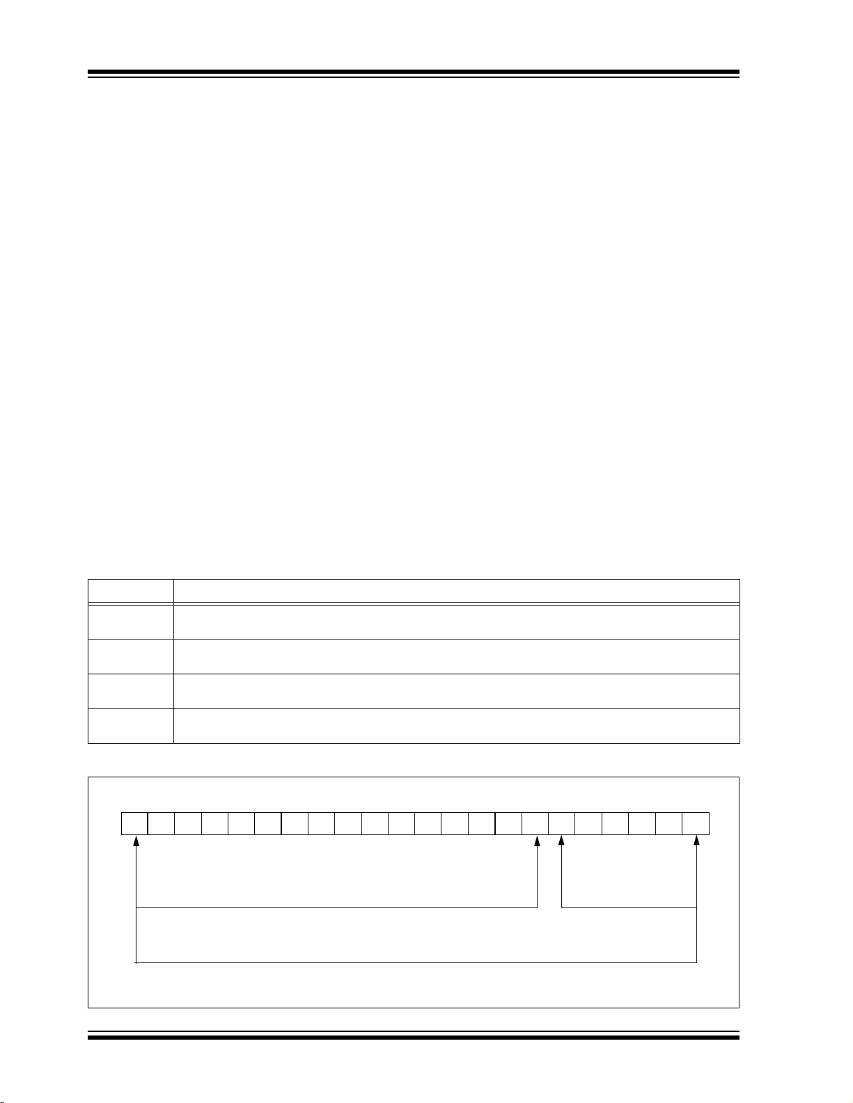
PIC18F2XK20/4XK20
21 16 15 87 0
TABLE ERASE/WRITE TABLE WRITE
TABLE READ – TBLPTR<21:0>
TBLPTRL
TBLPTRH
TBLPTRU
TBLPTR<n:0>
(1)
TBLPTR<21:n+1>
(1)
Note 1: n = 3, 4, 5, or 6 for block sizes of 8, 16, 32 or 64 bytes, respectively.
6.2.2 TABLAT – TABLE LATCH REGISTER
The Table Latch (TABLAT) is an 8-bit register mapped
into the SFR space. The Table Latch register is used to
hold 8-bit data during data transfers between program
memory and data RAM.
6.2.3 TBLPTR – TABLE POINTER REGISTER
The Table Pointer (TBLPTR) register addresses a byte
within the program memory. The TBLPTR is comprised
of t hree S FR registers: T able Pointer U pper Byte,
Table Poi nter High Byte and Table Poin ter Low Byte
(TBLPTRU:TBLPTRH:TBLPTRL). The se thre e re gisters join to f orm a 22-bit w ide pointer. The lo w-order
21 bits allow the device to address up to 2 Mbytes of
program memory space. The 22nd bit allows access to
the device ID, the user ID and the Configuration bits.
The Table Poi nter regi ster, TBL PTR, is us ed by th e
TBLRD and TBLWT instructions. These instructions can
update the TBLPTR in one of four ways based on the
table op eration. Th ese o perations are sh own i n
Table 6-2. These operations on the TBLPTR affect only
the low-order 21 bits.
6.2.4 TABLE POINTER BOUNDARIES
TBLPTR is used in rea ds, writes and erases of the
Flash program memory.
When a TBLRD is executed, all 22 bits of the TBLPTR
determine w hich b yte is r ead f rom pr ogram m emory
directly into the TABLAT register.
When a TBLWT is executed the byte in the TABLAT register is written, not to Flash memory but, to a holding
register in preparation for a program memory write. The
holding registers constitute a w rite block which varies
depending on the device (See Table 6-1).The 3, 4, or 5
LSbs of the TBLPTRL register determine which specific
address within the holding register block is written to.
The MSBs of the Table Pointer h ave no effect during
TBLWT operations.
When a p rogram memory write is executed the entire
holding register block is written to the Flash memory at
the address determined by the MSbs of the TBLPTR.
The 3, 4, or 5 LSBs are ignored during Flash memory
writes. Fo r m ore de tail, see Section 6.5 “Writing to
Flash Program Memory”.
When an e rase of program memory is executed, the
16 MSbs o f t he Table Po inter register
(TBLPTR<21:6>) point to the 64-byte block that will be
erased. The Least Significant bits (TBLPTR<5:0>) are
ignored.
Figure 6-3 de scribes t he re levant bo undaries of
TBLPTR based on Flash program memory operations.
TABLE 6-2: TABLE POINTER OPERATIONS WITH TBLRD AND TBLWT INSTRUCTIONS
Example Operation on Table Pointer
TBLRD*
TBLWT*
TBLRD*+
TBLWT*+
TBLRD*TBLWT*-
TBLRD+*
TBLWT+*
TBLPTR is incremented after the read/write
TBLPTR is decremented after the read/write
TBLPTR is incremented before the read/write
TBLPTR is not modified
FIGURE 6-3: TABLE POINTER BOUNDARIES BASED ON OPERATION
DS41303G-page 92 2010 Microchip Technology Inc.

PIC18F2XK20/4XK20
(Even Byte Address)
Program Memory
(Odd Byte Address)
TBLRD
TAB LAT
TBLPTR = xxx xx1
FETCH
Instruction Register
(IR)
Read Register
TBLPTR = xxxxx0
MOVLW CODE_ADDR_UPPER ; Load TBLPTR with the base
MOVWF TBLPTRU ; address of the word
MOVLW CODE_ADDR_HIGH
MOVWF TBLPTRH
MOVLW CODE_ADDR_LOW
MOVWF TBLPTRL
READ_WORD
TBLRD*+ ; read into TABLAT and increment
MOVF TABLAT, W ; get data
MOVWF WORD_EVEN
TBLRD*+ ; read into TABLAT and increment
MOVFW TABLAT, W ; get data
MOVF WORD_ODD
6.3 Reading the Flash Program Memory
The TBLRD in struction ret rieves da ta from pro gram
memory and places it into data RAM. Table reads from
The internal program memory is typically organized by
words. The Least Significant bit of the address selects
between the high and low bytes of the word. Figure 6-4
shows t he i nterface b etween th e in ternal pr ogram
memory and the TABLAT.
program memory are performed one byte at a time.
TBLPTR p oints to a byte address in program space.
Executing TBLRD pl aces the by te pointed to in to
TABLAT. In a ddition, T BLPTR c an b e m odified
automatically for the next table read operation.
FIGURE 6-4: READS FROM FLASH PROGRAM MEMORY
EXAMPLE 6-1: READING A FLASH PROGRAM MEMORY WORD
2010 Microchip Technology Inc. DS41303G-page 93

PIC18F2XK20/4XK20
MOVLW CODE_ADDR_UPPER ; load TBLPTR with the base
MOVWF TBLPTRU ; address of the memory block
MOVLW CODE_ADDR_HIGH
MOVWF TBLPTRH
MOVLW CODE_ADDR_LOW
MOVWF TBLPTRL
ERASE_BLOCK
BSF EECON1, EEPGD ; point to Flash program memory
BCF EECON1, CFGS ; access Flash program memory
BSF EECON1, WREN ; enable write to memory
BSF EECON1, FREE ; enable block Erase operation
BCF INTCON, GIE ; disable interrupts
Required MOVLW 55h
Sequence MOVWF EECON2 ; write 55h
MOVLW 0AAh
MOVWF EECON2 ; write 0AAh
BSF EECON1, WR ; start erase (CPU stall)
BSF INTCON, GIE ; re-enable interrupts
6.4 Erasing Flash Program Memory
The minimum erase block is 32 words or 64 bytes. Only
through the use of an external programmer, or through
ICSP™ control, can larger blocks of program memory
be bulk erased. Word erase in t he Flash array is not
supported.
When initiating an erase sequence from the Microcontroller itself, a block of 64 bytes of program memory is
erased. Th e Mo st Si gnificant 16 bi ts of the
TBLPTR<21:6> p oint t o the block being erased. Th e
TBLPTR<5:0> bits are ignored.
The EECON1 register commands the erase operation.
The EEPGD bit must be set to point to the Flash program memory. The WR EN bit must be set to en able
write operations. The FREE bit is set to select an erase
operation.
The w rite in itiate s equence fo r EEC ON2, sh own a s
steps 4 thro ugh 6 in Section 6.4.1 “Flash Program
Memory Erase Sequence”, is used to guard against
accidental w rites. Thi s is so metimes referred to as a
long write.
A long write is necessary for erasing the internal Flash.
Instruction ex ecution is ha lted d uring t he long w rite
cycle. The long write is terminated by the internal programming timer.
6.4.1 FLASH PROGRAM MEMORY ERASE SEQUENCE
The sequence of events for erasing a block of internal
program memory is:
1. Load T able Poi nter reg ister with address of
block being erased.
2. Set the EECON1 register for the erase operation:
• set EEPGD bit to point to program memory;
• clear the CFGS bit to access program memory;
• set WREN bit to enable writes;
• set FREE bit to enable the erase.
3. Disable interrupts.
4. Write 55h to EECON2.
5. Write 0AAh to EECON2.
6. Set the WR bit. This will begin the block erase
cycle.
7. The C PU w ill st all for duration of th e erase
(about 2 ms using internal timer).
8. Re-enable interrupts.
EXAMPLE 6-2: ERASING A FLASH PROGRAM MEMORY BLOCK
DS41303G-page 94 2010 Microchip Technology Inc.

PIC18F2XK20/4XK20
TABLAT
TBLPTR = xxxx YY
(1)
TBLPTR = xxxx01TBLPTR = xxxx00
Write Register
TBLPTR = xxxx0 2
Program Memory
Holding Register Holding Register Holding Register Holding Register
8
8 8 8
Note 1: YY = x7, xF, or 1F for 8, 16 or 32 byte write blocks, respectively.
6.5 Writing to Flash Program Memory
The p rogramming block s ize is 1 6, 3 2 o r 64 by tes,
depending on the device (See Table 6-1). Word or byte
programming is not supported.
Table w rites a re us ed i nternally to loa d the hol ding
registers needed to program the Flash memory. There
are only as many holding registers as there are bytes
in a write block (See Table 6-1).
Since the Table Latch (TABLAT) is only a single byte,
the TBLWT instruction may need to be executed 16, 32
or 64 ti mes, depending on the de vice, fo r e ach programming ope ration. All of the t able w rite operations
will essentially be short writes because only the holding
registers are written. After all the holding registers have
been written, the programming operation of that block
of memory is started by configuring the EECON1 register for a prog ram memory write and performing the
long write sequence.
The long write is necessary for programming the internal Flash. Instruction execution is halted during a long
write c ycle. The l ong w rite w ill be te rminated b y th e
internal programming timer.
The EEPRO M on-c hip tim er c ontrols the write time.
The write/erase voltages are generated by an on-chip
charge pump, rated to operate over the voltage range
of the device.
Note: The default value of the holding registers on
device Resets and after write operations is
FFh. A w rite of FF h t o a ho lding register
does not modify that byte. This means that
individual bytes of program memory may be
modified, provided that the change does not
attempt to change any bit from a ‘0’ to a ‘1’.
When mod ifying in dividual bytes, it is not
necessary to lo ad al l holding re gisters
before executing a long write operation.
FIGURE 6-5: TABLE WRITES TO FLASH PROGRAM MEMORY
6.5.1 FLASH PROGRAM MEMORY WRITE SEQUENCE
The sequence o f events for programming an internal
program memory location should be:
1. Read 64 bytes into RAM.
2. Update data values in RAM as necessary.
3. Load Table Pointer register with address being
erased.
4. Execute the block erase procedure.
5. Load Table Pointer register with address of first
byte being written.
6. Write the 16, 32 or 64 byte block into the holding
registers with auto-increment.
7. Set the EECON1 register for the write operation:
• set EEPGD bit to point to program memory;
• clear the CFGS bit to access program memory;
• set WREN to enable byte writes.
2010 Microchip Technology Inc. DS41303G-page 95
8. Disable interrupts.
9. Write 55h to EECON2.
10. Write 0AAh to EECON2.
11. Set the WR bit. This will begin the write cycle.
12. The CPU will stall for duration of the write (about
2 ms using internal timer).
13. Re-enable interrupts.
14. Repeat steps 6 to 13 for each block until all 64
bytes are written.
15. Verify the memory (table read).
This procedure will require about 6 ms to update each
write block of memory. An example of the required code
is given in Example 6-3.
Note: Before s etting the WR bit , the T able
Pointer add ress nee ds to be w ithin the
intended address range of the bytes in the
holding registers.

PIC18F2XK20/4XK20
MOVLW D'64’ ; number of bytes in erase block
MOVWF COUNTER
MOVLW BUFFER_ADDR_HIGH ; point to buffer
MOVWF FSR0H
MOVLW BUFFER_ADDR_LOW
MOVWF FSR0L
MOVLW CODE_ADDR_UPPER ; Load TBLPTR with the base
MOVWF TBLPTRU ; address of the memory block
MOVLW CODE_ADDR_HIGH
MOVWF TBLPTRH
MOVLW CODE_ADDR_LOW
MOVWF TBLPTRL
READ_BLOCK
TBLRD*+ ; read into TABLAT, and inc
MOVF TABLAT, W ; get data
MOVWF POSTINC0 ; store data
DECFSZ COUNTER ; done?
BRA READ_BLOCK ; repeat
MODIFY_WORD
MOVLW BUFFER_ADDR_HIGH ; point to buffer
MOVWF FSR0H
MOVLW BUFFER_ADDR_LOW
MOVWF FSR0L
MOVLW NEW_DATA_LOW ; update buffer word
MOVWF POSTINC0
MOVLW NEW_DATA_HIGH
MOVWF INDF0
ERASE_BLOCK
MOVLW CODE_ADDR_UPPER ; load TBLPTR with the base
MOVWF TBLPTRU ; address of the memory block
MOVLW CODE_ADDR_HIGH
MOVWF TBLPTRH
MOVLW CODE_ADDR_LOW
MOVWF TBLPTRL
BSF EECON1, EEPGD ; point to Flash program memory
BCF EECON1, CFGS ; access Flash program memory
BSF EECON1, WREN ; enable write to memory
BSF EECON1, FREE ; enable Erase operation
BCF INTCON, GIE ; disable interrupts
MOVLW 55h
Required MOVWF EECON2 ; write 55h
Sequence MOVLW 0AAh
MOVWF EECON2 ; write 0AAh
BSF EECON1, WR ; start erase (CPU stall)
BSF INTCON, GIE ; re-enable interrupts
TBLRD*- ; dummy read decrement
MOVLW BUFFER_ADDR_HIGH ; point to buffer
MOVWF FSR0H
MOVLW BUFFER_ADDR_LOW
MOVWF FSR0L
WRITE_BUFFER_BACK
MOVLW BlockSize ; number of bytes in holding register
MOVWF COUNTER
MOVLW D’64’/BlockSize ; number of write blocks in 64 bytes
MOVWF COUNTER2
WRITE_BYTE_TO_HREGS
MOVF POSTINC0, W ; get low byte of buffer data
MOVWF TABLAT ; present data to table latch
TBLWT+* ; write data, perform a short write
; to internal TBLWT holding register.
EXAMPLE 6-3: WRITING TO FLASH PROGRAM MEMORY
DS41303G-page 96 2010 Microchip Technology Inc.

PIC18F2XK20/4XK20
DECFSZ COUNTER ; loop until holding registers are full
BRA WRITE_WORD_TO_HREGS
PROGRAM_MEMORY
BSF EECON1, EEPGD ; point to Flash program memory
BCF EECON1, CFGS ; access Flash program memory
BSF EECON1, WREN ; enable write to memory
BCF INTCON, GIE ; disable interrupts
MOVLW 55h
Required MOVWF EECON2 ; write 55h
Sequence MOVLW 0AAh
MOVWF EECON2 ; write 0AAh
BSF EECON1, WR ; start program (CPU stall)
DCFSZ COUNTER2 ; repeat for remaining write blocks
BRA WRITE_BYTE_TO_HREGS ;
BSF INTCON, GIE ; re-enable interrupts
BCF EECON1, WREN ; disable write to memory
EXAMPLE 6-3: WRITING TO FLASH PROGRAM MEMORY (CONTINUED)
6.5.2 WRITE VERIFY
Depending o n th e a pplication, good p rogramming
practice m ay di ctate tha t th e v alue written t o th e
memory should be v erified against the original value.
This should be used in a pplications where excessive
writes can stress bits near the specification limit.
6.5.3 UNEXPECTED TERMINATION OF WRITE OPERATION
If a write is terminated by an unplanned event, such as
loss of power or an une xpected R eset, the me mory
location ju st p rogrammed sh ould be ver ified an d
reprogrammed if n eeded. If the w rite ope ration i s
interrupted by a MCLR Reset or a WDT Time-out Reset
during n ormal op eration, t he WRERR b it w ill be s et
which the user can check to decide whether a rewrite
of the location(s) is needed.
TABLE 6-3: REGISTERS ASSOCIATED WITH PROGRAM FLASH MEMORY
Name Bit 7 Bit 6 Bit 5 Bit 4 Bit 3 Bit 2 Bit 1 Bit 0
TBLPTRU — — bit 21 Program Memory Table Pointer Upper Byte (TBLPTR<20:16>) 59
TBPLTRH Program Memory Table Pointer High Byte (TBLPTR<15:8>) 59
TBLPTRL Program Memory Table Pointer Low Byte (TBLPTR<7:0>) 59
TABLAT Program Memory Table Latch 59
INTCON GIE/GIEH PEIE/GIEL TMR0IE INT0IE RBIE TMR0IF INT0IF RBIF 59
EECON2 EEPROM Control Register 2 (not a physical register) 61
EECON1 EEPGD CFGS
IPR2
PIR2
PIE2 OSCFIE C1IE C2IE EEIE BCLIE HLVDIE TMR3IE CCP2IE 62
Legend: — = unimplemented, read as ‘0’. Shaded cells are not used during Flash/EEPROM access.
2010 Microchip Technology Inc. DS41303G-page 97
OSCFIP C1IP C2IP EEIP BCLIP HLVDIP TMR3IP CCP2IP 62
OSCFIF C1IF C2IF EEIF BCLIF HLVDIF TMR3IF CCP2IF 62
6.5.4 PROTECTION AGAINST SPURIOUS WRITES
To prot ect against spu rious w rites to Flash pro gram
memory, the w rite ini tiate sequence must als o be
followed. See Section 23.0 “Special Features of the
CPU” for more detail.
6.6 Flash Program Operation During
Code Protection
See Section 23.3 “Program Verification and Code
Protection” for details on c ode p rotection of Fl ash
program memory.
Reset
Values on
page
— FREE WRERR WREN WR RD 61

PIC18F2XK20/4XK20
NOTES:
DS41303G-page 98 2010 Microchip Technology Inc.

PIC18F2XK20/4XK20
7.0 DATA EEPROM MEMORY
The data EEPROM is a nonvolatile memory array, separate from the data RAM and program memory, which
is used for long-term storage of program data. It is not
directly mapped i n either the register fi le or program
memory space but is indirectly addressed through the
Special Function Reg isters (SF Rs). The EEPROM i s
readable and writable during normal operation over the
entire V
Four SFR s are u sed to re ad an d w rite to th e da ta
EEPROM as well as the program memory. They are:
• EECON1
• EECON2
• EEDATA
• EEADR
• EEADRH
The data EEPROM allows byte read and write. When
interfacing to th e data memory block, E EDATA ho lds
the 8-bit data for read/write and the EEADR:EEADRH
register pair hold the address of the EEPROM location
being accessed.
The EEPROM data memory is rated for high erase/write
cycle endurance. A byte write automatically erases the
location and w rites the new data (er ase-before-write).
The write time is controlled by an on-chip time r; it w ill
vary with voltage and temperature as well as from chipto-chip. Please refer to parameter D122 (Table 26.10 in
Section 26.0 “Electrical Characteristics”) for e xact
limits.
DD range.
The EECON1 register (Register 7-1) is the control register for data and program memory access. Control bit
EEPGD determines if the access will be to program or
data EEPROM memory. When the EEPGD bit is clear,
operations wil l ac cess the da ta EEPROM m emory.
When the EEPGD b it is s et, program m emory i s
accessed.
Control bit, CFGS, determines if the access will be to
the Configuration registers or to program memory/data
EEPROM memory. Whe n the CFGS b it is s et,
subsequent operations access Configuration registers.
When the CFGS b it is clear, t he EEPGD bit s elects
either program Flash or data EEPROM memory.
The WREN bit, when set, will allow a write operation.
On power-up, the WREN bit is clear.
The WRERR bit is set by hardware when the WR bit is
set and cleared when the internal programming timer
expires and the write operation is complete.
Note: During norm al op eration, the WR ERR
may read as ‘1’. This can indicate that a
write o peration w as prematurely t erminated by a Reset, or a write operation was
attempted improperly.
The WR control bit ini tiates write ope rations. The bit
can be set but not cleared by software. It is cleared only
by hardware at the completion of the write operation.
Note: The EEIF in terrupt fl ag bi t of the PIR 2
register is set when the write is complete.
It must be cleared by software.
7.1 EEADR and EEADRH Registers
The EEAD R reg ister is us ed to add ress th e da ta
EEPROM for read and write op erations. Th e 8-b it
range of the register can address a memory range of
256 bytes (00h to FFh). The EEADRH register expands
the range to 1024 bytes by adding an additional two
address bits.
7.2 EECON1 and EECON2 Registers
Access to th e data EEPROM i s controlled b y two
registers: EECON1 and EECON2. These are the same
registers which control access to the program memory
and are used in a s imilar manner fo r the da ta
EEPROM.
Control bi ts, RD and WR , star t read an d er ase/write
operations, respectively. These bits are set by firmware
and c leared by ha rdware at the completion of th e
operation.
The RD bit cannot be se t when acc essing program
memory (EEPGD = 1). Program memory is read using
table read instructions. See Section 6.1 “Tabl e Reads
and Table Writes” regarding table reads.
The EECON2 regi ster is not a physical register. It i s
used e xclusively in t he memory w rite a nd erase
sequences. Reading EECON2 will read all ‘0’s.
2010 Microchip Technology Inc. DS41303G-page 99

PIC18F2XK20/4XK20
REGISTER 7-1: EECON1: DATA EEPROM CONTROL 1 REGISTER
R/W-x R/W-x U-0 R/W -0 R/W-x R/W-0 R/S-0 R/S-0
EEPGD CFGS — FREE WRERR WREN WR RD
bit 7 bit 0
Legend:
R = Readable bit W = Writable bit
S = Bit can be set by software, but not cleared U = Unimplemented bit, read as ‘0’
-n = Value at POR ‘1’ = Bit is set ‘0’ = Bit is cleared x = Bit is unknown
bit 7 EEPGD: Flash Program or Data EEPROM Memory Select bit
1 = Access Flash program memory
0 = Access data EEPROM memory
bit 6 CFGS: Flash Program/Data EEPROM or Configuration Select bit
1 = Access Configuration registers
0 = Access Flash program or data EEPROM memory
bit 5 Unimplemented: Read as ‘0’
bit 4 FREE: Flash Row (Block) Erase Enable bit
1 = Erase the program memory block addressed by TBLPTR on the next WR command
(cleared by completion of erase operation)
0 = Perform write-only
bit 3 WRERR: Flash Program/Data EEPROM Error Flag bit
1 = A write operation is prematurely terminated (any Reset during self-timed programming in normal
operation, or an improper write attempt)
0 = The write operation completed
(1)
bit 2 WREN: Flash Program/Data EEPROM Write Enable bit
1 = Allows write cycles to Flash program/data EEPROM
0 = Inhibits write cycles to Flash program/data EEPROM
bit 1 WR: Write Control bit
1 = Initiates a data EEPROM erase/write cycle or a program memory erase cycle or write cycle.
(The operation is self-timed and the bit is cleared by hardware once write is complete.
The WR bit can only be set (not cleared) by software.)
0 = Write cycle to the EEPROM is complete
bit 0 RD: Read Control bit
1 = Initiates an EEPROM read (Read takes one cycle. RD is cleared by hardware. The RD bit can only
be set (not cleared) by software. RD bit cannot be set when EEPGD = 1 or CFGS = 1.)
0 = Does not initiate an EEPROM read
Note 1: When a WRERR occurs, the EEPGD and CFGS bits are not cleared. This allows tracing of the
error condition.
DS41303G-page 100 2010 Microchip Technology Inc.
 Loading...