

PIC18F2420/2520/4420/4520
Data Sheet
28/40/44-Pin Enhanced Flash
Microcontrollers with 10-Bit A/D
and nanoWatt Technology
© 2008 Microchip Technology Inc. DS39631E
Note the following details of the code protection feature on Microchip devices:
• Microchip products meet the specification contained in their particular Microchip Data Sheet.
• Microchip believes that its family of products is one of the most secure families of its kind on the market today, when used in the
intended manner and under normal conditions.
• There are dishonest and possibly illegal methods used to breach the code protection feature. All of these methods, to our
knowledge, require using the Microchip products in a manner outside the operating specifications contained in Microchip’s Data
Sheets. Most likely, the person doing so is engaged in theft of intellectual property.
• Microchip is willing to work with the customer who is concerned about the integrity of their code.
• Neither Microchip nor any other semiconductor manufacturer can guarantee the security of their code. Code protection does not
mean that we are guaranteeing the product as “unbreakable.”
Code protection is constantly evolving. We at Microchip are committed to continuously improving the code protection features of our
products. Attempts to break Microchip’s code protection feature may be a violation of the Digital Millennium Copyright Act. If such acts
allow unauthorized access to your software or other copyrighted work, you may have a right to sue for relief under that Act.
Information contained in this publication regarding device
applications and the like is provided only for your convenience
and may be superseded by updates. It is your responsibility to
ensure that your application meets with your specifications.
MICROCHIP MAKES NO REPRESENTATIONS OR
WARRANTIES OF ANY KIND WHETHER EXPRESS OR
IMPLIED, WRITTEN OR ORAL, STATUTORY OR
OTHERWISE, RELATED TO THE INFORMATION,
INCLUDING BUT NOT LIMITED TO ITS CONDITION,
QUALITY, PERFORMANCE, MERCHANTABILITY OR
FITNESS FOR PURPOSE. Microchip disclaims all liability
arising from this information and its use. Use of Microchip
devices in life support and/or safety applications is entirely at
the buyer’s risk, and the buyer agrees to defend, indemnify and
hold harmless Microchip from any and all damages, claims,
suits, or expenses resulting from such use. No licenses are
conveyed, implicitly or otherwise, under any Microchip
intellectual property rights.
Trademarks
The Microchip name and logo, the Microchip logo, Accuron,
dsPIC, K
EELOQ, KEELOQ logo, MPLAB, PIC, PICmicro,
PICSTART, rfPIC, SmartShunt and UNI/O are registered
trademarks of Microchip Technology Incorporated in the
U.S.A. and other countries.
FilterLab, Linear Active Thermistor, MXDEV, MXLAB,
SEEVAL, SmartSensor and The Embedded Control Solutions
Company are registered trademarks of Microchip Technology
Incorporated in the U.S.A.
Analog-for-the-Digital Age, Application Maestro, CodeGuard,
dsPICDEM, dsPICDEM.net, dsPICworks, dsSPEAK, ECAN,
ECONOMONITOR, FanSense, In-Circuit Serial
Programming, ICSP, ICEPIC, Mindi, MiWi, MPASM, MPLAB
Certified logo, MPLIB, MPLINK, mTouch, PICkit, PICDEM,
PICDEM.net, PICtail, PIC
32
logo, PowerCal, PowerInfo,
PowerMate, PowerTool, REAL ICE, rfLAB, Select Mode, Total
Endurance, WiperLock and ZENA are trademarks of
Microchip Technology Incorporated in the U.S.A. and other
countries.
SQTP is a service mark of Microchip Technology Incorporated
in the U.S.A.
All other trademarks mentioned herein are property of their
respective companies.
© 2008, Microchip Technology Incorporated, Printed in the
U.S.A., All Rights Reserved.
Printed on recycled paper.
Microchip received ISO/TS-16949:2002 certification for its worldwide
headquarters, design and wafer fabrication facilities in Chandler and
Tempe, Arizona; Gresham, Oregon and design centers in California
and India. The Company’s quality system processes and procedures
are for its PIC
devices, Serial EEPROMs, microperipherals, nonvolatile memory and
analog products. In addition, Microchip’s quality system for the design
and manufacture of development systems is ISO 9001:2000 certified.
®
MCUs and dsPIC® DSCs, KEELOQ
®
code hopping
DS39631E-page ii © 2008 Microchip Technology Inc.
PIC18F2420/2520/4420/4520
28/40/44-Pin Enhanced Flash Microcontrollers with
10-Bit A/D and nanoWatt Technology
Power Management Features:
• Run: CPU on, Peripherals on
• Idle: CPU off, Peripherals on
• Sleep: CPU off, Peripherals off
• Ultra Low 50nA Input Leakage
• Run mode Currents Down to 11 μA Typical
• Idle mode Currents Down to 2.5 μA Typical
• Sleep mode Current Down to 100 nA Typical
• Timer1 Oscillator: 900 nA, 32 kHz, 2V
• Watchdog Timer: 1.4 μA, 2V Typical
• Two-Speed Oscillator Start-up
Flexible Oscillator Struc ture:
• Four Crystal modes, up to 40 MHz
• 4x Phase Lock Loop (PLL) – Available for Crystal
and Internal Oscillators
• Two External RC modes, up to 4 MHz
• Two External Clock modes, up to 40 MHz
• Internal Oscillator Block:
- Fast wake from Sleep and Idle, 1 μs typical
- 8 use-selectable frequencies, from 31 kHz to
8MHz
- Provides a complete range of clock speeds
from 31 kHz to 32 MHz when used with PLL
- User-tunable to compensate for frequency drift
• Secondary Oscillator using Timer1 @ 32 kHz
• Fail-Safe Clock Monitor:
- Allows for safe shutdown if peripheral clock stops
Peripheral Highlights:
• High-Current Sink/Source 25 mA/25 mA
• Three Programmable External Interrupts
• Four Input Change Interrupts
• Up to 2 Capture/Compare/PWM (CCP) modules,
one with Auto-Shutdown (28-pin devices)
• Enhanced Capture/Compare/PWM (ECCP)
module (40/44-pin devices only):
- One, two or four PWM outputs
- Selectable polarity
- Programmable dead time
- Auto-shutdown and auto-restart
-
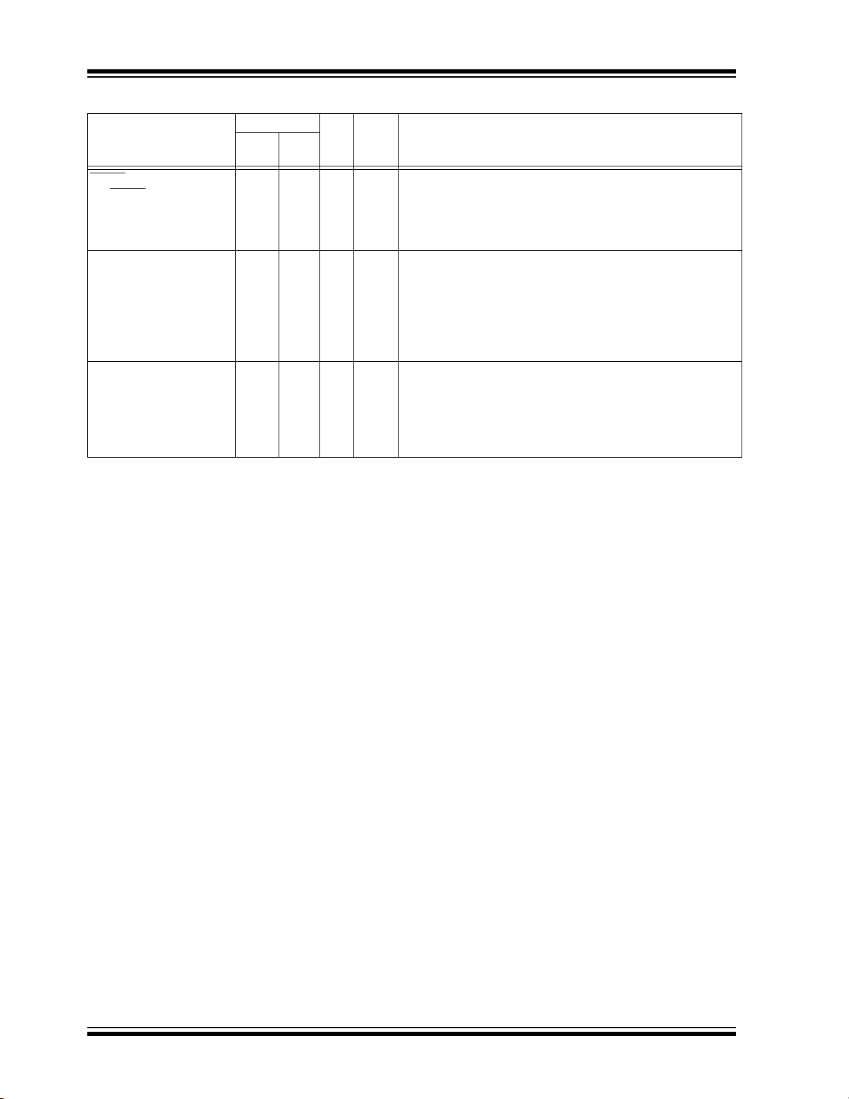
Program Memory Data Memory
Device
PIC18F2420 16K 8192 768 256 25 10 2/0 Y Y 1 2 1/3
PIC18F2520 32K 16384 1536 256 25 10 2/0 Y Y 1 2 1/3
PIC18F4420 16K 8192 768 256 36 13 1/1 Y Y 1 2 1/3
PIC18F4520 32K 16384 1536 256 36 13 1/1 Y Y 1 2 1/3
Flash
(bytes)
# Single-Word
Instructions
SRAM
(bytes)
EEPROM
(bytes)
Peripheral Highlight s (Continued):
• Master Synchronous Serial Port (MSSP) module
Supporting 3-Wire SPI (all 4 modes) and I
Master and Slave modes
• Enhanced Addressable USART module:
- Supports RS-485, RS-232 and LIN/J2602
- RS-232 operation using internal oscillator
block (no external crystal required)
- Auto-wake-up on Start bit
- Auto-Baud Detect
• 10-Bit, up to 13-Channel Analog-to-Digital (A/D)
Converter module:
- Auto-acquisition capability
- Conversion available during Sleep
• Dual Analog Comparators with Input Multiplexing
• Programmable 16-Level High/Low-Voltage
Detection (HLVD) module:
- Supports interrupt on High/Low-Voltage Detection
Special Microcontroller Features:
• C Compiler Optimized Architecture:
- Optional extended instruction set designed to
optimize re-entrant code
• 100,000 Erase/Write Cycle Enhanced Flash
Program Memory Typical
• 1,000,000 Erase/Write Cycle Data EEPROM
Memory Typical
• Flash/Data EEPROM Retention: 100 Years Typical
• Self-Programmable under Software Control
• Priority Levels for Interrupts
• 8 x 8 Single-Cycle Hardware Multiplier
• Extended Watchdog Timer (WDT):
- Programmable period from 4 ms to 131s
• Single-Supply 5V In-Circuit Serial
Programming™ (ICSP™) via Two Pins
• In-Circuit Debug (ICD) via Two Pins
• Wide Operating Voltage Range: 2.0V to 5.5V
• Programmable Brown-out Reset (BOR) with
Software Enable Option
I/O
10-Bit
A/D (ch)
CCP/
ECCP
(PWM)
SPI
MSSP
Master
2
I
C™
EUSART
Comp.
2
C™
Timers
8/16-Bit
© 2008 Microchip Technology Inc. DS39631E-page 1
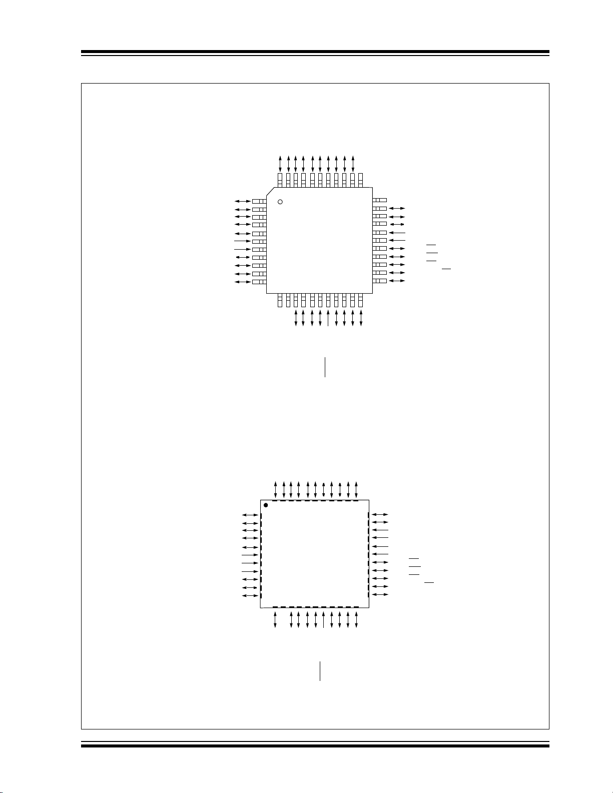
PIC18F2420/2520/4420/4520
PIC18F2520
10
11
2
3
4
5
6
1
8
7
9
12
13
14
15
16
17
18
19
20
23
24
25
26
27
28
22
21
MCLR/VPP/RE3
RA0/AN0
RA1/AN1
RA2/AN2/V
REF-/CVREF
RA3/AN3/VREF+
RA4/T0CKI/C1OUT
RA5/AN4/SS
/HLVDIN/C2OUT
V
SS
OSC1/CLKI/RA7
OSC2/CLKO/RA6
RC0/T1OSO/T13CKI
RC1/T1OSI/CCP2
(1)
RC2/CCP1
RC3/SCK/SCL
RB7/KBI3/PGD
RB6//KBI2/PGC
RB5/KBI1/PGM
RB4/KBI0/AN11
RB3/AN9/CCP2
(1)
RB2/INT2/AN8
RB1/INT1/AN10
RB0/INT0/FLT0/AN12
V
DD
VSS
RC7/RX/DT
RC6/TX/CK
RC5/SDO
RC4/SDI/SDA
28-Pin SPDIP, SOIC
PIC18F2420
Note 1: RB3 is the alternate pin for CCP2 multiplexing.
10 11
2
3
6
1
18
19
20
21
22
12 13 14
15
8
7
16
17
232425262728
9
PIC18F2420
RC0/T1OSO/T13CKI
5
4
RB7/KBI3/PGD
RB6/KBI2/PGC
RB5/KBI1/PGM
RB4KBI0/AN11
RB3/AN9/CCP2
(1)
RB2/INT2/AN8
RB1/INT1/AN10
RB0/INT0/FLT0/AN12
V
DD
VSS
RC7/RX/DT
RC6/TX/CK
RC5/SDO
RC4/SDI/SDA
MCLR
/VPP/RE3
RA0/AN0
RA1/AN1
RA2/AN2/VREF-/CVREF
RA3/AN3/VREF+
RA4/T0CKI/C1OUT
RA5/AN4/SS
/HLVDIN/C2OUT
V
SS
OSC1/CLKI/RA7
OSC2/CLKO/RA6
RC1/T1OSI/CCP2
(1)
RC2/CCP1
RC3/SCK/SCL
PIC18F2520
28-Pin QFN
RB7/KBI3/PGD
RB6/KBI2/PGC
RB5/KBI1/PGM
RB4/KBI0/AN11
RB3/AN9/CCP2
(1)
RB2/INT2/AN8
RB1/INT1/AN10
RB0/INT0/FLT0/AN12
V
DD
VSS
RD7/PSP7/P1D
RD6/PSP6/P1C
RD5/PSP5/P1B
RD4/PSP4
RC7/RX/DT
RC6/TX/CK
RC5/SDO
RC4/SDI/SDA
RD3/PSP3
RD2/PSP2
MCLR/VPP/RE3
RA0/AN0
RA1/AN1
RA2/AN2/V
REF-/CVREF
RA3/AN3/VREF+
RA4/T0CKI/C1OUT
RA5/AN4/SS
/HLVDIN/C2OUT
RE0/RD
/AN5
RE1/WR
/AN6
RE2/CS
/AN7
V
DD
VSS
OSC1/CLKI/RA7
OSC2/CLKO/RA6
RC0/T1OSO/T13CKI
RC1/T1OSI/CCP2
(1)
RC2/CCP1/P1A
RC3/SCK/SCL
RD0/PSP0
RD1/PSP1
1
2
3
4
5
6
7
8
9
10
11
12
13
14
15
16
17
18
19
20
40
39
38
37
36
35
34
33
32
31
30
29
28
27
26
25
24
23
22
21
PIC18F4520
40-Pin PDIP
PIC18F4420
Pin Diagrams
DS39631E-page 2 © 2008 Microchip Technology Inc.
Pin Diagrams (Cont.’d)
Note 1: RB3 is the alternate pin for CCP2 multiplexing.
10
11
2
3
4
5
6
1
1819202122
121314
15
38
8
7
4443424140
39
16
17
29
30
31
32
33
23
24
25
26
27
28
363435
9
PIC18F4420
37
RA3/AN3/V
REF+
RA2/AN2/V
REF-/CVREF
RA1/AN1
RA0/AN0
MCLR
/VPP/RE3
RB3/AN9/CCP2
(1)
RB7/KBI3/PGD
RB6/KBI2/PGC
RB5/KBI1/PGM
RB4/KBI0/AN11
NC
RC6/TX/CK
RC5/SDO
RC4/SDI/SDA
RD3/PSP3
RD2/PSP2
RD1/PSP1
RD0/PSP0
RC3/SCK/SCL
RC2/CCP1/P1A
RC1/T1OSI/CCP2
(1)
RC0/T1OSO/T13CKI
OSC2/CLKO/RA6
OSC1/CLKI/RA7
V
SS
VSS
VDD
VDD
RE2/CS/AN7
RE1/WR
/AN6
RE0/RD
/AN5
RA5/AN4/SS
/HLVDIN/C2OUT
RA4/T0CKI/C1OUT
RC7/RX/DT
RD4/PSP4
RD5/PSP5/P1B
RD6/PSP6/P1C
RD7/PSP7/P1D
V
SS
VDD
VDD
RB0/INT0/FLT0/AN12
RB1/INT1/AN10
RB2/INT2/AN8
44-pin QFN
PIC18F4520
10
11
2
3
4
5
6
1
1819202122
121314
15
38
8
7
4443424140
39
16
17
29
30
31
32
33
23
24
25
26
27
28
363435
9
PIC18F4420
37
RA3/AN3/VREF+
RA2/AN2/V
REF-/CVREF
RA1/AN1
RA0/AN0
MCLR
/VPP/RE3
NC
RB7/KBI3/PGD
RB6/KBI2/PGC
RB5/KBI1/PGM
RB4/KBI0/AN11
NC
RC6/TX/CK
RC5/SDO
RC4/SDI/SDA
RD3/PSP3
RD2/PSP2
RD1/PSP1
RD0/PSP0
RC3/SCK/SCL
RC2/CCP1/P1A
RC1/T1OSI/CCP2
(1)
NC
NC
RC0/T1OSO/T13CKI
OSC2/CLKO/RA6
OSC1/CLKI/RA7
V
SS
VDD
RE2/CS/AN7
RE1/WR
/AN6
RE0/RD
/AN5
RA5/AN4/SS
/HLVDIN/C2OUT
RA4/T0CKI/C1OUT
RC7/RX/DT
RD4/PSP4
RD5/PSP5/P1B
RD6/PSP6/P1C
RD7/PSP7/P1D
V
SS
VDD
RB0/INT0/FLT0/AN12
RB1/INT1/AN10
RB2/INT2/AN8
RB3/AN9/CCP2
(1)
44-pin TQFP
PIC18F4520
PIC18F2420/2520/4420/4520
© 2008 Microchip Technology Inc. DS39631E-page 3

PIC18F2420/2520/4420/4520
Table of Contents
1.0 Device Overview .......................................................................................................................................................................... 7
2.0 Oscillator Configurations ............................................................................................................................................................ 23
3.0 Power-Managed Modes ............................................................................................................................................................. 33
4.0 Reset .......................................................................................................................................................................................... 41
5.0 Memory Organization ................................................................................................................................................................. 53
6.0 Flash Program Memory.............................................................................................................................................................. 73
7.0 Data EEPROM Memory ............................................................................................................................................................. 83
8.0 8 x 8 Hardware Multiplier............................................................................................................................................................ 89
9.0 Interrupts .................................................................................................................................................................................... 91
10.0 I/O Ports ................................................................................................................................................................................... 105
11.0 Timer0 Module ......................................................................................................................................................................... 123
12.0 Timer1 Module ......................................................................................................................................................................... 127
13.0 Timer2 Module ......................................................................................................................................................................... 133
14.0 Timer3 Module ......................................................................................................................................................................... 135
15.0 Capture/Compare/PWM (CCP) Modules ................................................................................................................................. 139
16.0 Enhanced Capture/Compare/PWM (ECCP) Module ................................................................................................................ 147
17.0 Master Synchronous Serial Port (MSSP) Module .................................................................................................................... 161
18.0 Enhanced Universal Synchronous Asynchronous Receiver Transmitter (EUSART) ............................................................... 201
19.0 10-Bit Analog-to-Digital Converter (A/D) Module ..................................................................................................................... 223
20.0 Comparator Module.................................................................................................................................................................. 233
21.0 Comparator Voltage Reference Module ................................................................................................................................... 239
22.0 High/Low-Voltage Detect (HLVD) ............................................................................................................................................. 243
23.0 Special Features of the CPU.................................................................................................................................................... 249
24.0 Instruction Set Summary .......................................................................................................................................................... 267
25.0 Development Support............................................................................................................................................................... 317
26.0 Electrical Characteristics .......................................................................................................................................................... 321
27.0 DC and AC Characteristics Graphs and Tables ....................................................................................................................... 361
28.0 Packaging Information.............................................................................................................................................................. 383
Appendix A: Revision History............................................................................................................................................................. 395
Appendix B: Device Differences......................................................................................................................................................... 395
Appendix C: Migration from Mid-Range to Enhanced Devices .......................................................................................................... 396
Appendix D: Migration from High-End to Enhanced Devices............................................................................................................. 396
Index .................................................................................................................................................................................................. 397
The Microchip Web Site..................................................................................................................................................................... 407
Customer Change Notification Service .............................................................................................................................................. 407
Customer Support .............................................................................................................................................................................. 407
Reader Response .............................................................................................................................................................................. 408
PIC18F2420/2520/4420/4520 Product Identification System ............................................................................................................ 409
DS39631E-page 4 © 2008 Microchip Technology Inc.

PIC18F2420/2520/4420/4520
TO OUR VALUED CUSTOMERS
It is our intention to provide our valued customers with the best documentation possible to ensure successful use of your Microchip
products. To this end, we will continue to improve our publications to better suit your needs. Our publications will be refined and
enhanced as new volumes and updates are introduced.
If you have any questions or comments regarding this publication, please contact the Marketing Communications Department via
E-mail at docerrors@microchip.com or fax the Reader Response Form in the back of this data sheet to (480) 792-4150. We
welcome your feedback.
Most Current Data Sheet
To obtain the most up-to-date version of this data sheet, please register at our Worldwide Web site at:
http://www.microchip.com
You can determine the version of a data sheet by examining its literature number found on the bottom outside corner of any page.
The last character of the literature number is the version number, (e.g., DS30000A is version A of document DS30000).
Errata
An errata sheet, describing minor operational differences from the data sheet and recommended workarounds, may exist for current
devices. As device/documentation issues become known to us, we will publish an errata sheet. The errata will specify the revision
of silicon and revision of document to which it applies.
To determine if an errata sheet exists for a particular device, please check with one of the following:
• Microchip’s Worldwide Web site; http://www.microchip.com
• Your local Microchip sales office (see last page)
When contacting a sales office, please specify which device, revision of silicon and data sheet (include literature number) you are
using.
Customer Notification System
Register on our web site at www.microchip.com to receive the most current information on all of our products.
© 2008 Microchip Technology Inc. DS39631E-page 5

PIC18F2420/2520/4420/4520
NOTES:
DS39631E-page 6 © 2008 Microchip Technology Inc.

PIC18F2420/2520/4420/4520
1.0 DEVICE OVERVIEW
This document contains device-specific information for
the following devices:
• PIC18F2420 • PIC18LF2420
• PIC18F2520 • PIC18LF2520
• PIC18F4420 • PIC18LF4420
• PIC18F4520 • PIC18LF4520
This family offers the advantages of all PIC18
microcontrollers – namely, high computational performance at an economical price – with the addition of
high-endurance, Enhanced Flash program memory.
On top of these features, the PIC18F2420/2520/4420/
4520 family introduces design enhancements that
make these microcontrollers a logical choice for many
high-performance, power sensitive applications.
1.1 New Core Features
1.1.1 nanoWatt TECHNOLOGY
All of the devices in the PIC18F2420/2520/4420/4520
family incorporate a range of features that can significantly reduce power consumption during operation.
Key items include:
• Alternate Run Modes: By clocking the controller
from the Timer1 source or the internal oscillator
block, power consumption during code execution
can be reduced by as much as 90%.
• Multiple Idle Modes: The controller can also run
with its CPU core disabled but the peripherals still
active. In these states, power consumption can be
reduced even further, to as little as 4% of normal
operation requirements.
• On-the-Fly Mode Switching: The power-
managed modes are invoked by user code during
operation, allowing the user to incorporate
power-saving ideas into their application’s
software design.
• Low Consumption in Key Modules: The
power requirements for both Timer1 and the
Watchdog Timer are minimized. See
Section 26.0 “Electrical Characteristics”
for values.
1.1.2 MULTIPLE OSCILLATOR OPTIONS AND FEATURES
All of the devices in the PIC18F2420/2520/4420/4520
family offer ten different oscillator options, allowing
users a wide range of choices in developing application
hardware. These include:
• Four Crystal modes, using crystals or ceramic
resonators
• Two External Clock modes, offering the option of
using two pins (oscillator input and a divide-by-4
clock output) or one pin (oscillator input, with the
second pin reassigned as general I/O)
• Two External RC Oscillator modes with the same
pin options as the External Clock modes
• An internal oscillator block which provides an
8 MHz clock and an INTRC source
(approximately 31 kHz), as well as a range of
6 user-selectable clock frequencies, between
125 kHz to 4 MHz, for a total of 8 clock
frequencies. This option frees the two oscillator
pins for use as additional general purpose I/O.
• A Phase Lock Loop (PLL) frequency multiplier,
available to both the High-Speed Crystal and Internal Oscillator modes, which allows clock speeds of
up to 40 MHz. Used with the internal oscillator, the
PLL gives users a complete selection of clock
speeds, from 31 kHz to 32 MHz – all without using
an external crystal or clock circuit.
Besides its availability as a clock source, the internal
oscillator block provides a stable reference source that
gives the family additional features for robust
operation:
• Fail-Safe Clock Monitor: This option constantly
monitors the main clock source against a reference signal provided by the internal oscillator. If a
clock failure occurs, the controller is switched to
the internal oscillator block, allowing for continued
low-speed operation or a safe application
shutdown.
• T wo-Speed Start-up: This option allows the
internal oscillator to serve as the clock source
from Power-on Reset, or wake-up from Sleep
mode, until the primary clock source is available.
© 2008 Microchip Technology Inc. DS39631E-page 7

PIC18F2420/2520/4420/4520
1.2 Other Special Features
• Memory Endurance: The Enhanced Flash cells
for both program memory and data EEPROM are
rated to last for many thousands of erase/write
cycles – up to 100,000 for program memory and
1,000,000 for EEPROM. Data retention without
refresh is conservatively estimated to be greater
than 40 years.
• Self-Programmability: These devices can write
to their own program memory spaces under
internal software control. By using a bootloader
routine located in the protected Boot Block at the
top of program memory, it becomes possible to
create an application that can update itself in the
field.
• Extended Instruction Set: The PIC18F2420/
2520/4420/4520 family introduces an optional
extension to the PIC18 instruction set, which adds
8 new instructions and an Indexed Addressing
mode. This extension, enabled as a device configuration option, has been specifically designed
to optimize re-entrant application code originally
developed in high-level languages, such as C.
• Enhanced CCP Module: In PWM mode, this
module provides 1, 2 or 4 modulated outputs for
controlling half-bridge and full-bridge drivers.
Other features include auto-shutdown, for disabling PWM outputs on interrupt, or other select
conditions, and auto-restart to reactivate outputs
once the condition has cleared.
• Enhanced Addressable USART: This serial
communication module is capable of standard
RS-232 operation and provides support for the LIN
bus protocol. Other enhancements include
automatic baud rate detection and a 16-bit Baud
Rate Generator for improved resolution. When the
microcontroller is using the internal oscillator
block, the EUSART provides stable operation for
applications that talk to the outside world without
using an external crystal (or its accompanying
power requirement).
• 10-Bit A/D Converter: This module incorporates
programmable acquisition time, allowing for a
channel to be selected and a conversion to be
initiated without waiting for a sampling period and
thus, reducing code overhead.
• Extended Watchdog Timer (WDT): This
enhanced version incorporates a 16-bit prescaler,
allowing an extended time-out range that is stable
across operating voltage and temperature. See
Section 26.0 “Electrical Characteristics” for
time-out periods.
1.3 Details on Individual Family Members
Devices in the PIC18F2420/2520/4420/4520 family are
available in 28-pin and 40/44-pin packages. Block
diagrams for the two groups are shown in Figure 1-1
and Figure 1-2.
The devices are differentiated from each other in five
ways:
1. Flash program memory (16 Kbytes for
PIC18F2420/4420 devices and 32 Kbytes for
PIC18F2520/4520 devices).
2. A/D channels (10 for 28-pin devices, 13 for
40/44-pin devices).
3. I/O ports (3 bidirectional ports on 28-pin devices,
5 bidirectional ports on 40/44-pin devices).
4. CCP and Enhanced CCP implementation
(28-pin devices have 2 standard CCP
modules, 40/44-pin devices have one standard
CCP module and one ECCP module).
5. Parallel Slave Port (present only on 40/44-pin
devices).
All other features for devices in this family are identical.
These are summarized in Table 1-1.
The pinouts for all devices are listed in Table 1-2 and
Table 1-3.
Like all Microchip PIC18 devices, members of the
PIC18F2420/2520/4420/4520 family are available as
both standard and low-voltage devices. Standard
devices with Enhanced Flash memory, designated with
an “F” in the part number (such as PIC18F2420),
accommodate an operating V
Low-voltage parts, designated by “LF” (such as
PIC18LF2420), function over an extended VDD range
of 2.0V to 5.5V.
DD range of 4.2V to 5.5V.
DS39631E-page 8 © 2008 Microchip Technology Inc.
PIC18F2420/2520/4420/4520
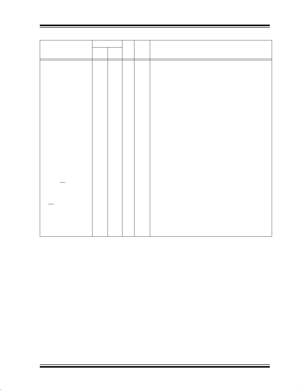
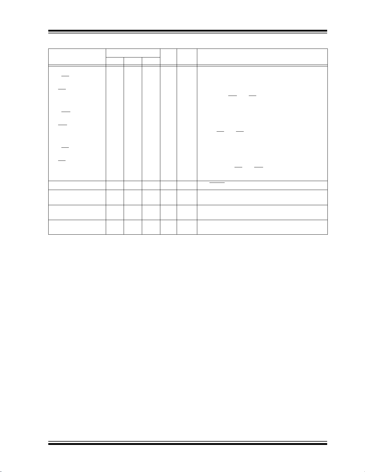
TABLE 1-1: DEVICE FEATURES
Features PIC18F2420 PIC18F2520 PIC18F4420 PIC18F4520
Operating Frequency DC – 40 MHz DC – 40 MHz DC – 40 MHz DC – 40 MHz
Program Memory (Bytes) 16384 32768 16384 32768
Program Memory
(Instructions)
Data Memory (Bytes) 768 1536 768 1536
Data EEPROM Memory (Bytes) 256 256 256 256
Interrupt Sources 19 19 20 20
I/O Ports Ports A, B, C, (E) Ports A, B, C, (E) Ports A, B, C, D, E Ports A, B, C, D, E
Timers 4 4 4 4
Capture/Compare/PWM Modules 2 2 1 1
Enhanced
Capture/Compare/PWM Modules
Serial Communications MSSP,
Parallel Communications (PSP) No No Yes Yes
10-Bit Analog-to-Digital Module 10 Input Channels 10 Input Channels 13 Input Channels 13 Input Channels
Resets (and Delays) POR, BOR,
Underflow (PWRT, OST),
Programmable
High/Low-Voltage Detect
Programmable Brown-out Reset Yes Yes Yes Yes
Instruction Set 75 Instructions;
Packages 28-Pin SPDIP
8192 16384 8192 16384
0011
Enhanced USART
RESET Instruction,
Stack Full, Stack
MCLR
(optional), WDT
Ye s Ye s Ye s Ye s
83 with Extended
Instruction Set Enabled
28-Pin SOIC
28-Pin QFN
MSSP,
Enhanced USART
POR, BOR,
RESET Instruction,
Stack Full, Stack
Underflow (PWRT, OST),
MCLR (optional), WDT
75 Instructions;
83 with Extended
Instruction Set Enabled
28-Pin SPDIP
28-Pin SOIC
28-Pin QFN
MSSP,
Enhanced USART
POR, BOR,
RESET Instruction,
Stack Full, Stack
Underflow (PWRT, OST),
MCLR (optional), WDT
75 Instructions;
83 with Extended
Instruction Set Enabled
40-Pin PDIP
44-Pin QFN
44-Pin TQFP
MSSP,
Enhanced USART
POR, BOR,
RESET Instruction,
Stack Full, Stack
Underflow (PWRT, OST),
MCLR (optional), WDT
75 Instructions;
83 with Extended
Instruction Set Enabled
40-Pin PDIP
44-Pin QFN
44-Pin TQFP
© 2008 Microchip Technology Inc. DS39631E-page 9
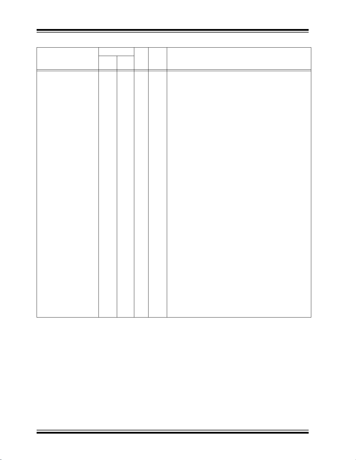
PIC18F2420/2520/4420/4520
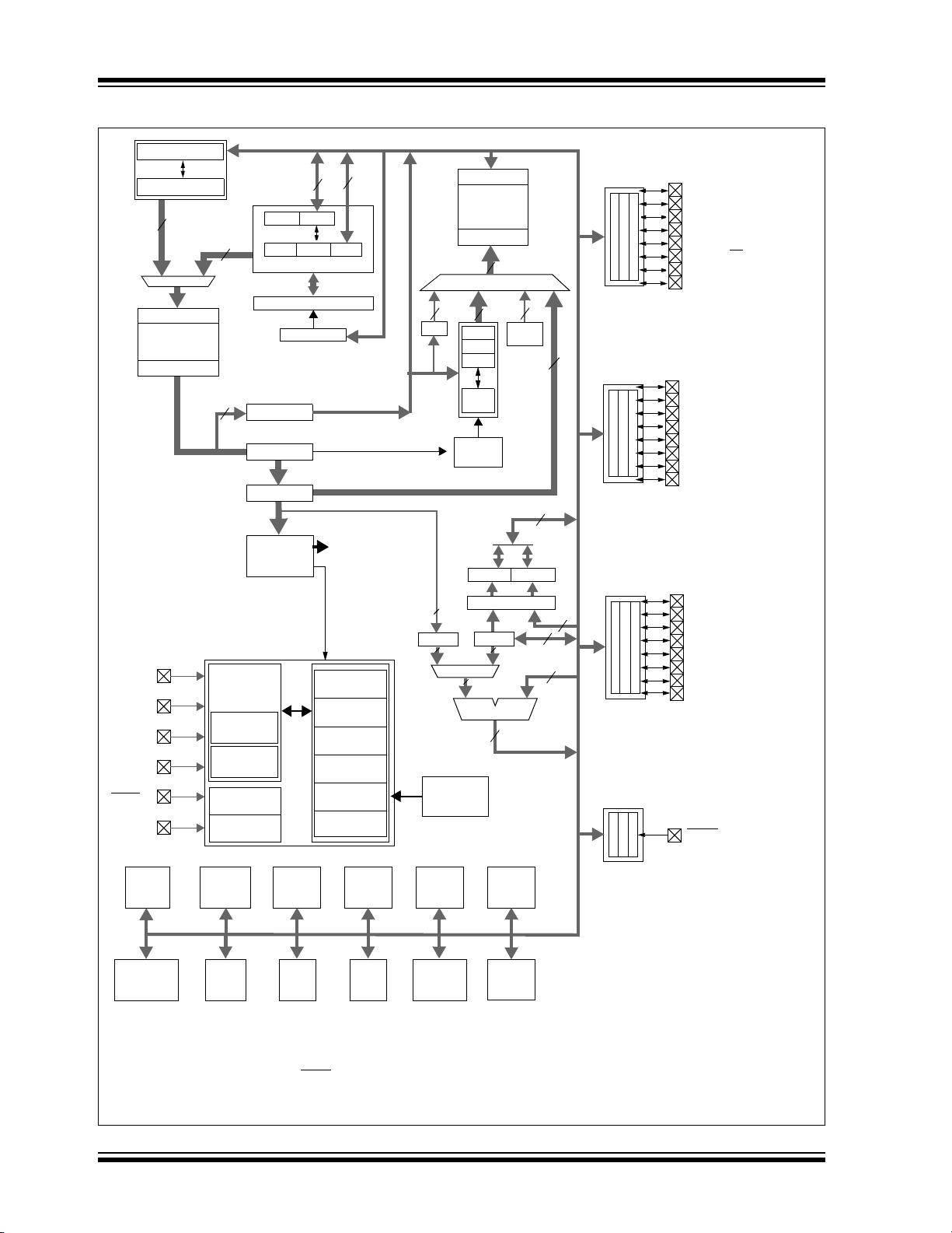
Instruction
Decode and
Control
PORTA
PORTB
PORTC
RA4/T0CKI/C1OUT
RA5/AN4/SS
/HLVDIN/C2OUT
RB0/INT0/FLT0/AN12
RC0/T1OSO/T13CKI
RC1/T1OSI/CCP2
(1)
RC2/CCP1
RC3/SCK/SCL
RC4/SDI/SDA
RC5/SDO
RC6/TX/CK
RC7/RX/DT
RA3/AN3/VREF+
RA2/AN2/VREF-/CVREF
RA1/AN1
RA0/AN0
RB1/INT1/AN10
Data Latch
Data Memory
( 3.9 Kbytes )
Address Latch
Data Address<12>
12
Access
BSR
FSR0
FSR1
FSR2
inc/dec
logic
Address
4
12
4
PCH PCL
PCLATH
8
31-Level Stack
Program Counter
PRODLPRODH
8 x 8 Multiply
8
BITOP
8
8
ALU<8>
Address Latch
Program Memory
(16/32 Kbytes)
Data Latch
20
8
8
Table Pointer<21>
inc/dec logic
21
8
Data Bus<8>
Table Latch
8
IR
12
3
ROM Latch
RB2/INT2/AN8
RB3/AN9/CCP2
(1)
PCLATU
PCU
OSC2/CLKO
(3)
/RA6
Note 1: CCP2 is multiplexed with RC1 when Configuration bit, CCP2MX, is set, or RB3 when CCP2MX is not set.
2: RE3 is only available when MCLR
functionality is disabled.
3: OSC1/CLKI and OSC2/CLKO are only available in select oscillator modes and when these pins are not being used as digital I/O.
Refer to Section 2.0 “Oscillator Configurations” for additional information.
RB4/KBI0/AN11
RB5/KBI1/PGM
RB6/KBI2/PGC
RB7/KBI3/PGD
EUSARTComparator
MSSP
10-Bit
ADC
Timer2Timer1 Timer3Timer0
CCP2
HLVD
CCP1
BOR
Data
EEPROM
W
Instruction Bus <16>
STKPTR
Bank
8
State Machine
Control Signals
Decode
8
8
Power-up
Timer
Oscillator
Start-up Timer
Power-on
Reset
Watchdog
Timer
OSC1
(3)
OSC2
(3)
VDD,
Brown-out
Reset
Internal
Oscillator
Fail-Safe
Clock Monitor
Precision
Reference
Band Gap
V
SS
MCLR
(2)
Block
INTRC
Oscillator
8 MHz
Oscillator
Single-Supply
Programming
In-Circuit
Debugger
T1OSO
OSC1/CLKI
(3)
/RA7
T1OSI
PORTE
MCLR/VPP/RE3
(2)
FIGURE 1-1: PIC18F2420/2520 ( 28-PIN) BLOCK DI AGRAM
DS39631E-page 10 © 2008 Microchip Technology Inc.
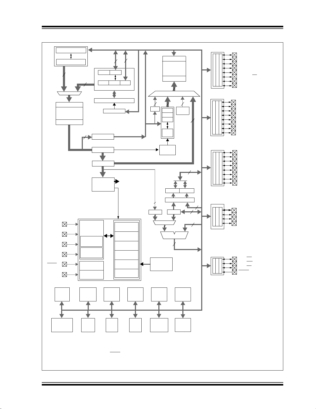
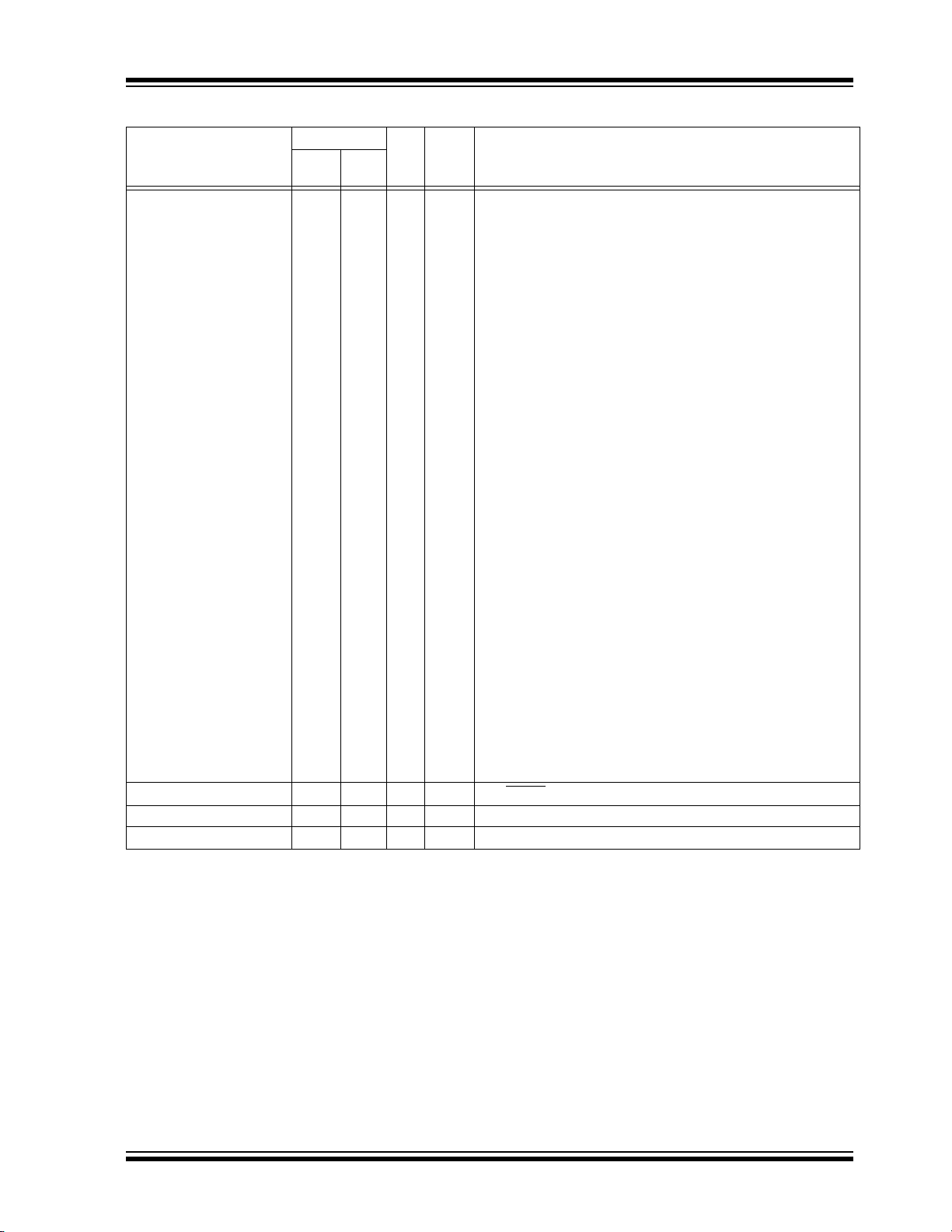
PIC18F2420/2520/4420/4520
Instruction
Decode and
Control
Data Latch
Data Memory
( 3.9 Kbytes )
Address Latch
Data Address<12>
12
Access
BSR
FSR0
FSR1
FSR2
inc/dec
logic
Address
4
12
4
PCH PCL
PCLATH
8
31-Level Stack
Program Counter
PRODLPRODH
8 x 8 Multiply
8
BITOP
8
8
ALU<8>
Address Latch
Program Memory
(16/32 Kbytes)
Data Latch
20
8
8
Table Pointer<21>
inc/dec logic
21
8
Data Bus<8>
Table Latch
8
IR
12
3
ROM Latch
PORTD
RD0/PSP0
PCLATU
PCU
PORTE
MCLR/VPP/RE3
(2)
RE2/CS/AN7
RE0/RD/AN5
RE1/WR/AN6
Note 1: CCP2 is multiplexed with RC1 when Configuration bit, CCP2MX, is set, or RB3 when CCP2MX is not set.
2: RE3 is only available when MCLR
functionality is disabled.
3: OSC1/CLKI and OSC2/CLKO are only available in select oscillator modes and when these pins are not being used as digital I/O.
Refer to Section 2.0 “Osc illa to r Config ura tions ” for additional information.
:RD4/PSP4
EUSARTComparator
MSSP
10-Bit
ADC
Timer2Timer1 Timer3Timer0
CCP2
HLVD
ECCP1
BOR
Data
EEPROM
W
Instruction Bus <16>
STKPTR
Bank
8
State Machine
Control Signals
Decode
8
8
Power-up
Timer
Oscillator
Start-up Timer
Power-on
Reset
Watchdog
Timer
OSC1
(3)
OSC2
(3)
VDD,
Brown-out
Reset
Internal
Oscillator
Fail-Safe
Clock Monitor
Precision
Reference
Band Gap
V
SS
MCLR
(2)
Block
INTRC
Oscillator
8 MHz
Oscillator
Single-Supply
Programming
In-Circuit
Debugger
T1OSI
T1OSO
RD5/PSP5/P1B
RD6/PSP6/P1C
RD7/PSP7/P1D
PORTA
PORTB
PORTC
RA4/T0CKI/C1OUT
RA5/AN4/SS
/HLVDIN/C2OUT
RB0/INT0/FLT0/AN12
RC0/T1OSO/T13CKI
RC1/T1OSI/CCP2
(1)
RC2/CCP1/P1A
RC3/SCK/SCL
RC4/SDI/SDA
RC5/SDO
RC6/TX/CK
RC7/RX/DT
RA3/AN3/VREF+
RA2/AN2/VREF-/CVREF
RA1/AN1
RA0/AN0
RB1/INT1/AN10
RB2/INT2/AN8
RB3/AN9/CCP2
(1)
OSC2/CLKO
(3)
/RA6
RB4/KBI0/AN11
RB5/KBI1/PGM
RB6/KBI2/PGC
RB7/KBI3/PGD
OSC1/CLKI
(3)
/RA7
FIGURE 1-2: PIC18F4420/452 0 ( 40/44 -P IN ) B LOCK DI AGR AM
© 2008 Microchip Technology Inc. DS39631E-page 11
PIC18F2420/2520/4420/4520
TABLE 1-2: PIC18F2420/2520 PINOUT I/O DESCRIPTIONS
Pin Number
Pin Name
MCLR
/VPP/RE3
MCLR
VPP
RE3
OSC1/CLKI/RA7
OSC1
CLKI
RA7
OSC2/CLKO/RA6
OSC2
CLKO
RA6
Legend: TTL = TTL compatible input CMOS = CMOS compatible input or output
ST = Schmitt Trigger input with CMOS levels I = Input
O = Output P = Power
Note 1: Default assignment for CCP2 when Configuration bit, CCP2MX, is set.
2: Alternate assignment for CCP2 when Configuration bit, CCP2MX, is cleared.
SPDIP ,
SOIC
126
96
10 7
QFN
Pin
Type
I
P
I
I
I
I/O
O
O
I/O
Buffer
Type
ST
ST
ST
CMOS
TTL
—
—
TTL
Description
Master Clear (input) or programming voltage (input).
Master Clear (Reset) input. This pin is an active-low
Reset to the device.
Programming voltage input.
Digital input.
Oscillator crystal or external clock input.
Oscillator crystal input or external clock source input.
ST buffer when configured in RC mode; CMOS otherwise.
External clock source input. Always associated with pin
function, OSC1. (See related OSC1/CLKI, OSC2/CLKO
pins.)
General purpose I/O pin.
Oscillator crystal or clock output.
Oscillator crystal output. Connects to crystal or
resonator in Crystal Oscillator mode.
In RC mode, OSC2 pin outputs CLKO which has 1/4 the
frequency of OSC1 and denotes the instruction cycle rate.
General purpose I/O pin.
DS39631E-page 12 © 2008 Microchip Technology Inc.
PIC18F2420/2520/4420/4520
TABLE 1-2: PIC18F2420/2520 PINOUT I/O DESCRIPTIONS (CONTINUED)
Pin Number
Pin Name
RA0/AN0
RA0
AN0
RA1/AN1
RA1
AN1
RA2/AN2/V
RA2
AN2
V
CV
RA3/AN3/V
RA3
AN3
V
RA4/T0CKI/C1OUT
RA4
T0CKI
C1OUT
RA5/AN4/SS
C2OUT
RA5
AN4
SS
HLVDIN
C2OUT
RA6 See the OSC2/CLKO/RA6 pin.
RA7 See the OSC1/CLKI/RA7 pin.
Legend: TTL = TTL compatible input CMOS = CMOS compatible input or output
Note 1: Default assignment for CCP2 when Configuration bit, CCP2MX, is set.
REF-/CVREF
REF-
REF
REF+
REF+
/HLVDIN/
ST = Schmitt Trigger input with CMOS levels I = Input
O = Output P = Power
2: Alternate assignment for CCP2 when Configuration bit, CCP2MX, is cleared.
SPDIP ,
SOIC
227
328
41
52
63
74
QFN
Pin
Buffer
Type
Type
I/OITTL
Analog
I/OITTL
Analog
I/O
TTL
I
Analog
I
Analog
O
Analog
I/O
TTL
I
Analog
I
Analog
I/O
I
O
I/O
TTL
I
Analog
I
TTL
I
Analog
O
PORTA is a bidirectional I/O port.
Digital I/O.
Analog input 0.
Digital I/O.
Analog input 1.
Digital I/O.
Analog input 2.
A/D reference voltage (low) input.
Comparator reference voltage output.
Digital I/O.
Analog input 3.
A/D reference voltage (high) input.
ST
ST
—
—
Digital I/O.
Timer0 external clock input.
Comparator 1 output.
Digital I/O.
Analog input 4.
SPI slave select input.
High/Low-Voltage Detect input.
Comparator 2 output.
Description
© 2008 Microchip Technology Inc. DS39631E-page 13
PIC18F2420/2520/4420/4520
TABLE 1-2: PIC18F2420/2520 PINOUT I/O DESCRIPTIONS (CONTINUED)
Pin Number
Pin Name
RB0/INT0/FLT0/AN12
RB0
INT0
FLT0
AN12
RB1/INT1/AN10
RB1
INT1
AN10
RB2/INT2/AN8
RB2
INT2
AN8
RB3/AN9/CCP2
RB3
AN9
(1)
CCP2
RB4/KBI0/AN11
RB4
KBI0
AN11
RB5/KBI1/PGM
RB5
KBI1
PGM
RB6/KBI2/PGC
RB6
KBI2
PGC
RB7/KBI3/PGD
RB7
KBI3
PGD
Legend: TTL = TTL compatible input CMOS = CMOS compatible input or output
ST = Schmitt Trigger input with CMOS levels I = Input
O = Output P = Power
Note 1: Default assignment for CCP2 when Configuration bit, CCP2MX, is set.
2: Alternate assignment for CCP2 when Configuration bit, CCP2MX, is cleared.
SPDIP ,
SOIC
21 18
22 19
23 20
24 21
25 22
26 23
27 24
28 25
QFN
Pin
Type
I/O
I
I
I
I/O
I
I
I/O
I
I
I/O
I
I/O
I/O
I
I
I/O
I
I/O
I/O
I
I/O
I/O
I
I/O
Buffer
Type
TTL
ST
ST
Analog
TTL
ST
Analog
TTL
ST
Analog
TTL
Analog
ST
TTL
TTL
Analog
TTL
TTL
ST
TTL
TTL
ST
TTL
TTL
ST
Description
PORTB is a bidirectional I/O port. PORTB can be software
programmed for internal weak pull-ups on all inputs.
Digital I/O.
External interrupt 0.
PWM Fault input for CCP1.
Analog input 12.
Digital I/O.
External interrupt 1.
Analog input 10.
Digital I/O.
External interrupt 2.
Analog input 8.
Digital I/O.
Analog input 9.
Capture 2 input/Compare 2 output/PWM2 output.
Digital I/O.
Interrupt-on-change pin.
Analog input 11.
Digital I/O.
Interrupt-on-change pin.
Low-Voltage ICSP™ Programming enable pin.
Digital I/O.
Interrupt-on-change pin.
In-Circuit Debugger and ICSP programming clock pin.
Digital I/O.
Interrupt-on-change pin.
In-Circuit Debugger and ICSP programming data pin.
DS39631E-page 14 © 2008 Microchip Technology Inc.
PIC18F2420/2520/4420/4520
TABLE 1-2: PIC18F2420/2520 PINOUT I/O DESCRIPTIONS (CONTINUED)
Pin Number
Pin Name
RC0/T1OSO/T13CKI
RC0
T1OSO
T13CKI
RC1/T1OSI/CCP2
RC1
T1OSI
(2)
CCP2
RC2/CCP1
RC2
CCP1
RC3/SCK/SCL
RC3
SCK
SCL
RC4/SDI/SDA
RC4
SDI
SDA
RC5/SDO
RC5
SDO
RC6/TX/CK
RC6
TX
CK
RC7/RX/DT
RC7
RX
DT
RE3 — — — — See MCLR
VSS 8, 19 5, 16 P — Ground reference for logic and I/O pins.
VDD 20 17 P — Positive supply for logic and I/O pins.
Legend: TTL = TTL compatible input CMOS = CMOS compatible input or output
ST = Schmitt Trigger input with CMOS levels I = Input
O = Output P = Power
Note 1: Default assignment for CCP2 when Configuration bit, CCP2MX, is set.
2: Alternate assignment for CCP2 when Configuration bit, CCP2MX, is cleared.
SPDIP ,
SOIC
11 8
12 9
13 10
14 11
15 12
16 13
17 14
18 15
QFN
Pin
Buffer
Type
Type
I/O
O
I
I/O
I
Analog
I/O
I/O
I/OSTST
I/O
I/O
I/O
I/O
I
I/O
I/OOST
I/O
O
I/O
I/O
I
I/O
PORTC is a bidirectional I/O port.
ST
—
ST
ST
ST
ST
ST
ST
ST
ST
ST
—
ST
—
ST
ST
ST
ST
Digital I/O.
Timer1 oscillator output.
Timer1/Timer3 external clock input.
Digital I/O.
Timer1 oscillator input.
Capture 2 input/Compare 2 output/PWM2 output.
Digital I/O.
Capture 1 input/Compare 1 output/PWM1 output.
Digital I/O.
Synchronous serial clock input/output for SPI mode.
Synchronous serial clock input/output for I
Digital I/O.
SPI data in.
I2C data I/O.
Digital I/O.
SPI data out.
Digital I/O.
EUSART asynchronous transmit.
EUSART synchronous clock (see related RX/DT).
Digital I/O.
EUSART asynchronous receive.
EUSART synchronous data (see related TX/CK).
/VPP/RE3 pin.
Description
2
C™ mode.
© 2008 Microchip Technology Inc. DS39631E-page 15
PIC18F2420/2520/4420/4520
TABLE 1-3: PIC18F4420/4520 PINOUT I/O DESCRIPTIONS
Pin Name
/VPP/RE3
MCLR
MCLR
VPP
RE3
OSC1/CLKI/RA7
OSC1
CLKI
RA7
OSC2/CLKO/RA6
OSC2
CLKO
RA6
Legend: TTL = TTL compatible input CMOS = CMOS compatible input or output
ST = Schmitt Trigger input with CMOS levels I = Input
O = Output P = Power
Note 1: Default assignment for CCP2 when Configuration bit, CCP2MX, is set.
2: Alternate assignment for CCP2 when Configuration bit, CCP2MX, is cleared.
Pin Number
PDIP QFN TQFP
11818
13 32 30
14 33 31
Pin
Type
I
P
I
I
I
I/O
O
O
I/O
Buffer
Type
ST
ST
ST
CMOS
TTL
—
—
TTL
Description
Master Clear (input) or programming voltage (input).
Master Clear (Reset) input. This pin is an active-low
Reset to the device.
Programming voltage input.
Digital input.
Oscillator crystal or external clock input.
Oscillator crystal input or external clock source input.
ST buffer when configured in RC mode;
analog otherwise.
External clock source input. Always associated with
pin function, OSC1. (See related OSC1/CLKI,
OSC2/CLKO pins.)
General purpose I/O pin.
Oscillator crystal or clock output.
Oscillator crystal output. Connects to crystal
or resonator in Crystal Oscillator mode.
In RC mode, OSC2 pin outputs CLKO which
has 1/4 the frequency of OSC1 and denotes
the instruction cycle rate.
General purpose I/O pin.
DS39631E-page 16 © 2008 Microchip Technology Inc.
PIC18F2420/2520/4420/4520
TABLE 1-3: PIC18F4420/4520 PINOUT I/O DESCRIPTIONS (CONTINUED)
Pin Name
RA0/AN0
RA0
AN0
RA1/AN1
RA1
AN1
RA2/AN2/V
RA3/AN3/V
RA4/T0CKI/C1OUT
RA5/AN4/SS
C2OUT
RA6 See the OSC2/CLKO/RA6 pin.
RA7 See the OSC1/CLKI/RA7 pin.
Legend: TTL = TTL compatible input CMOS = CMOS compatible input or output
Note 1: Default assignment for CCP2 when Configuration bit, CCP2MX, is set.
REF-/CVREF
RA2
AN2
VREF-
REF
CV
REF+
RA3
AN3
REF+
V
RA4
T0CKI
C1OUT
/HLVDIN/
RA5
AN4
SS
HLVDIN
C2OUT
ST = Schmitt Trigger input with CMOS levels I = Input
O = Output P = Power
2: Alternate assignment for CCP2 when Configuration bit, CCP2MX, is cleared.
Pin Number
PDIP QFN TQFP
21919
32020
42121
52222
62323
72424
Pin
Buffer
Type
Type
I/OITTL
Analog
I/OITTL
Analog
I/O
TTL
I
Analog
I
Analog
O
Analog
I/O
TTL
I
Analog
I
Analog
I/O
I
O
I/O
TTL
I
Analog
I
TTL
I
Analog
O
PORTA is a bidirectional I/O port.
Digital I/O.
Analog input 0.
Digital I/O.
Analog input 1.
Digital I/O.
Analog input 2.
A/D reference voltage (low) input.
Comparator reference voltage output.
Digital I/O.
Analog input 3.
A/D reference voltage (high) input.
ST
ST
—
—
Digital I/O.
Timer0 external clock input.
Comparator 1 output.
Digital I/O.
Analog input 4.
SPI slave select input.
High/Low-Voltage Detect input.
Comparator 2 output.
Description
© 2008 Microchip Technology Inc. DS39631E-page 17

PIC18F2420/2520/4420/4520
TABLE 1-3: PIC18F4420/4520 PINOUT I/O DESCRIPTIONS (CONTINUED)
Pin Name
RB0/INT0/FLT0/AN12
RB0
INT0
FLT0
AN12
RB1/INT1/AN10
RB1
INT1
AN10
RB2/INT2/AN8
RB2
INT2
AN8
RB3/AN9/CCP2
RB3
AN9
(1)
CCP2
RB4/KBI0/AN11
RB4
KBI0
AN11
RB5/KBI1/PGM
RB5
KBI1
PGM
RB6/KBI2/PGC
RB6
KBI2
PGC
RB7/KBI3/PGD
RB7
KBI3
PGD
Legend: TTL = TTL compatible input CMOS = CMOS compatible input or output
ST = Schmitt Trigger input with CMOS levels I = Input
O = Output P = Power
Note 1: Default assignment for CCP2 when Configuration bit, CCP2MX, is set.
2: Alternate assignment for CCP2 when Configuration bit, CCP2MX, is cleared.
Pin Number
PDIP QFN TQFP
33 9 8
34 10 9
35 11 10
36 12 11
37 14 14
38 15 15
39 16 16
40 17 17
Pin
Type
I/O
I
I
I
I/O
I
I
I/O
I
I
I/O
I
I/O
I/O
I
I
I/O
I
I/O
I/O
I
I/O
I/O
I
I/O
Buffer
Type
TTL
ST
ST
Analog
TTL
ST
Analog
TTL
ST
Analog
TTL
Analog
ST
TTL
TTL
Analog
TTL
TTL
ST
TTL
TTL
ST
TTL
TTL
ST
Description
PORTB is a bidirectional I/O port. PORTB can be
software programmed for internal weak pull-ups on all
inputs.
Digital I/O.
External interrupt 0.
PWM Fault input for Enhanced CCP1.
Analog input 12.
Digital I/O.
External interrupt 1.
Analog input 10.
Digital I/O.
External interrupt 2.
Analog input 8.
Digital I/O.
Analog input 9.
Capture 2 input/Compare 2 output/PWM2 output.
Digital I/O.
Interrupt-on-change pin.
Analog input 11.
Digital I/O.
Interrupt-on-change pin.
Low-Voltage ICSP™ Programming enable pin.
Digital I/O.
Interrupt-on-change pin.
In-Circuit Debugger and ICSP programming
clock pin.
Digital I/O.
Interrupt-on-change pin.
In-Circuit Debugger and ICSP programming
data pin.
DS39631E-page 18 © 2008 Microchip Technology Inc.
PIC18F2420/2520/4420/4520
TABLE 1-3: PIC18F4420/4520 PINOUT I/O DESCRIPTIONS (CONTINUED)
Pin Name
RC0/T1OSO/T13CKI
RC0
T1OSO
T13CKI
RC1/T1OSI/CCP2
RC1
T1OSI
(2)
CCP2
RC2/CCP1/P1A
RC2
CCP1
P1A
RC3/SCK/SCL
RC3
SCK
SCL
RC4/SDI/SDA
RC4
SDI
SDA
RC5/SDO
RC5
SDO
RC6/TX/CK
RC6
TX
CK
RC7/RX/DT
RC7
RX
DT
Legend: TTL = TTL compatible input CMOS = CMOS compatible input or output
ST = Schmitt Trigger input with CMOS levels I = Input
O = Output P = Power
Note 1: Default assignment for CCP2 when Configuration bit, CCP2MX, is set.
2: Alternate assignment for CCP2 when Configuration bit, CCP2MX, is cleared.
Pin Number
PDIP QFN TQFP
15 34 32
16 35 35
17 36 36
18 37 37
23 42 42
24 43 43
25 44 44
26 1 1
Pin
Type
I/O
O
I
I/O
I
I/O
I/O
I/O
O
I/O
I/O
I/O
I/O
I
I/O
I/O
O
I/O
O
I/O
I/O
I
I/O
Buffer
Type
ST
—
ST
ST
CMOS
ST
ST
ST
—
ST
ST
ST
ST
ST
ST
ST
—
ST
—
ST
ST
ST
ST
Description
PORTC is a bidirectional I/O port.
Digital I/O.
Timer1 oscillator output.
Timer1/Timer3 external clock input.
Digital I/O.
Timer1 oscillator input.
Capture 2 input/Compare 2 output/PWM2 output.
Digital I/O.
Capture 1 input/Compare 1 output/PWM1 output.
Enhanced CCP1 output.
Digital I/O.
Synchronous serial clock input/output for
SPI mode.
Synchronous serial clock input/output for I
Digital I/O.
SPI data in.
2
C data I/O.
I
Digital I/O.
SPI data out.
Digital I/O.
EUSART asynchronous transmit.
EUSART synchronous clock (see related RX/DT).
Digital I/O.
EUSART asynchronous receive.
EUSART synchronous data (see related TX/CK).
2
C™ mode.
© 2008 Microchip Technology Inc. DS39631E-page 19
PIC18F2420/2520/4420/4520
TABLE 1-3: PIC18F4420/4520 PINOUT I/O DESCRIPTIONS (CONTINUED)
Pin Name
RD0/PSP0
RD0
PSP0
RD1/PSP1
RD1
PSP1
RD2/PSP2
RD2
PSP2
RD3/PSP3
RD3
PSP3
RD4/PSP4
RD4
PSP4
RD5/PSP5/P1B
RD5
PSP5
P1B
RD6/PSP6/P1C
RD6
PSP6
P1C
RD7/PSP7/P1D
RD7
PSP7
P1D
Legend: TTL = TTL compatible input CMOS = CMOS compatible input or output
ST = Schmitt Trigger input with CMOS levels I = Input
O = Output P = Power
Note 1: Default assignment for CCP2 when Configuration bit, CCP2MX, is set.
2: Alternate assignment for CCP2 when Configuration bit, CCP2MX, is cleared.
Pin Number
PDIP QFN TQFP
19 38 38
20 39 39
21 40 40
22 41 41
27 2 2
28 3 3
29 4 4
30 5 5
Pin
Buffer
Type
Type
I/O
I/OSTTTL
I/O
I/OSTTTL
I/O
I/OSTTTL
I/O
I/OSTTTL
I/O
I/OSTTTL
I/O
I/O
TTL
O
I/O
I/O
TTL
O
I/O
I/O
TTL
O
Description
PORTD is a bidirectional I/O port or a Parallel Slave
Port (PSP) for interfacing to a microprocessor port.
These pins have TTL input buffers when PSP module
is enabled.
Digital I/O.
Parallel Slave Port data.
Digital I/O.
Parallel Slave Port data.
Digital I/O.
Parallel Slave Port data.
Digital I/O.
Parallel Slave Port data.
Digital I/O.
Parallel Slave Port data.
ST
—
ST
—
ST
—
Digital I/O.
Parallel Slave Port data.
Enhanced CCP1 output.
Digital I/O.
Parallel Slave Port data.
Enhanced CCP1 output.
Digital I/O.
Parallel Slave Port data.
Enhanced CCP1 output.
DS39631E-page 20 © 2008 Microchip Technology Inc.
PIC18F2420/2520/4420/4520
TABLE 1-3: PIC18F4420/4520 PINOUT I/O DESCRIPTIONS (CONTINUED)
Pin Name
RE0/RD
RE1/WR/AN6
RE2/CS/AN7
RE3 — — — — — See MCLR
VSS 12, 31 6, 30, 316, 29 P — Ground reference for logic and I/O pins.
/AN5
RE0
RD
AN5
RE1
WR
AN6
RE2
CS
AN7
Pin Number
PDIP QFN TQFP
82525
92626
10 27 27
Pin
Type
I/O
I
I
I/O
I
I
I/O
I
I
Buffer
Type
ST
TTL
Analog
ST
TTL
Analog
ST
TTL
Analog
Description
PORTE is a bidirectional I/O port.
Digital I/O.
Read control for Parallel Slave Port
(see also WR
Analog input 5.
Digital I/O.
Write control for Parallel Slave Port
(see CS
Analog input 6.
Digital I/O.
Chip Select control for Parallel Slave Port
(see related RD
Analog input 7.
and CS pins).
and RD pins).
and WR).
/VPP/RE3 pin.
V
DD 11, 32 7, 8,
28, 29
NC — 13 12, 13,
Legend: TTL = TTL compatible input CMOS = CMOS compatible input or output
ST = Schmitt Trigger input with CMOS levels I = Input
O = Output P = Power
Note 1: Default assignment for CCP2 when Configuration bit, CCP2MX, is set.
2: Alternate assignment for CCP2 when Configuration bit, CCP2MX, is cleared.
7, 28 P — Positive supply for logic and I/O pins.
— — No Connect.
33, 34
© 2008 Microchip Technology Inc. DS39631E-page 21

PIC18F2420/2520/4420/4520
NOTES:
DS39631E-page 22 © 2008 Microchip Technology Inc.
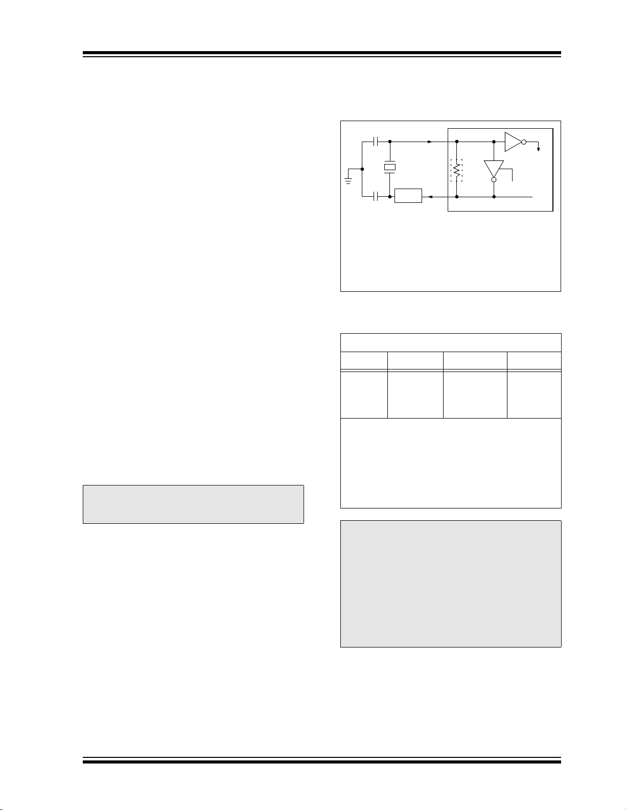
PIC18F2420/2520/4420/4520
Note 1: See Table 2-1 and Table 2-2 for initial values of
C1 and C2.
2: A series resistor (R
S) may be required for AT
strip cut crystals.
3: R
F varies with the oscillator mode chosen.
C1
(1)
C2
(1)
XTAL
OSC2
OSC1
RF
(3)
Sleep
To
Logic
PIC18FXXXX
RS
(2)
Internal
2.0 OSCILLATOR CONFIGURATIONS
FIGURE 2-1: CRYSTAL/CERAMIC
RESONATOR OPERATION
(XT, LP , HS O R HSP LL
2.1 Oscillator Types
PIC18F2420/2520/4420/4520 devices can be operated
in ten different oscillator modes. The user can program
the Configuration bits, FOSC<3:0>, in Configuration
Register 1H to select one of these ten modes:
1. LP Low-Power Crystal
2. XT Crystal/Resonator
3. HS High-Speed Crystal/Resonator
4. HSPLL High-Speed Crystal/Resonator
with PLL Enabled
5. RC External Resistor/Capacitor with
F
OSC/4 Output on RA6
6. RCIO External Resistor/Capacitor with I/O
on RA6
7. INTIO1 Internal Oscillator with F
on RA6 and I/O on RA7
8. INTIO2 Internal Oscillator with I/O on RA6
and RA7
9. EC External Clock with F
10. ECIO External Clock with I/O on RA6
2.2 Crystal Oscillator/Ceramic Resonators
In XT, LP, HS or HSPLL Oscillator modes, a crystal or
ceramic resonator is connected to the OSC1 and
OSC2 pins to establish oscillation. Figure 2-1 shows
the pin connections.
The oscillator design requires the use of a parallel cut
crystal.
Note: Use of a series cut crystal may give a fre-
quency out of the crystal manufacturer’s
specifications.
OSC/4 Output
OSC/4 Output
T ABLE 2-1: CAPACITOR SELECTION FOR
Typical Capacitor Values Used:
Mode Freq OSC1 OSC2
XT 3.58 MHz
4.19 MHz
Capacitor values are for design guidance only.
Different capacitor values may be required to produce
acceptable oscillator operation. The user should test
the performance of the oscillator over the expected
DD and temperature range for the application.
V
See the notes following Table 2-2 for additional
information.
Note: When using resonators with frequencies
above 3.5 MHz, the use of HS mode,
rather than XT mode, is recommended.
HS mode may be used at any V
which the controller is rated. If HS is
selected, it is possible that the gain of the
oscillator will overdrive the resonator.
Therefore, a series resistor should be
placed between the OSC2 pin and the
resonator. As a good starting point, the
recommended value of R
CONFIGURATION)
CERAMIC RESONATORS
15 pF
15 pF
4 MHz
4 MHz
30 pF
50 pF
S is 330Ω.
15 pF
15 pF
30 pF
50 pF
DD for
© 2008 Microchip Technology Inc. DS39631E-page 23

PIC18F2420/2520/4420/4520
OSC1
OSC2
Open
Clock from
Ext. System
PIC18FXXXX
(HS Mode)
OSC1/CLKI
OSC2/CLKO
F
OSC/4
Clock from
Ext. System
PIC18FXXXX
OSC1/CLKI
I/O (OSC2)
RA6
Clock from
Ext. System
PIC18FXXXX
TABLE 2-2: CAPACITOR SELECTION FOR
CRYSTAL OSCILLATOR
Osc T y pe
Crystal
Freq
LP 32 kHz 30 pF 30 pF
XT 1 MHz
4 MHz
HS 4 MHz
10 MHz
20 MHz
25 MHz
25 MHz
Capacitor values are for design guidance only.
These capacitors were tested with the crystals listed
below for basic start-up and operation. These values
are not optimized.
Different capacitor values may be required to produce
acceptable oscillator operation. The user should test
the performance of the oscillator over the expected
DD and temperature range for the application.
V
See the notes following this table for additional
information.
32 kHz 4 MHz
25 MHz 10 MHz
1 MHz 20 MHz
T ypical Cap acitor V alues
Tested:
C1 C2
15 pF
15 pF
15 pF
15 pF
15 pF
0 pF
15 pF
Crystals Used:
15 pF
15 pF
15 pF
15 pF
15 pF
5 pF
15 pF
An external clock source may also be connected to the
OSC1 pin in the HS mode, as shown in Figure 2-2.
FIGURE 2-2: EXTERNAL CLOCK INPUT
OPERATION (HS OSC
CONFIGURATION)
2.3 External Clock Input
The EC and ECIO Oscillator modes require an external
clock source to be connected to the OSC1 pin. There is
no oscillator start-up time required after a Power-on
Reset or after an exit from Sleep mode.
In the EC Oscillator mode, the oscillator frequency
divided by 4 is available on the OSC2 pin. This signal
may be used for test purposes or to synchronize other
logic. Figure 2-3 shows the pin connections for the EC
Oscillator mode.
FIGURE 2-3: EXTERNAL CLO CK
INPUT OPERATION
(EC CONFIGURATION)
Note 1: Higher capacitance increases the stability
of the oscillator but also increases the
start-up time.
2: When operating below 3V V
DD, or when
using certain ceramic resonators at any
voltage, it may be necessary to use the
HS mode or switch to a crystal oscillator.
3: Since each resonator/crystal has its own
characteristics, the user should consult
the resonator/crystal manufacturer for
appropriate values of external
components.
4: Rs may be required to avoid overdriving
crystals with low drive level specification.
5: Always verify oscillator performance over
DD and temperature range that is
the V
expected for the application.
The ECIO Oscillator mode functions like the EC mode,
except that the OSC2 pin becomes an additional general purpose I/O pin. The I/O pin becomes bit 6 of
PORTA (RA6). Figure 2-4 shows the pin connections
for the ECIO Oscillator mode.
FIGURE 2-4: EXTERNAL CLO CK
INPUT OPERATION
(ECIO CONFIG URAT ION)
DS39631E-page 24 © 2008 Microchip Technology Inc.

PIC18F2420/2520/4420/4520
OSC2/CLKO
CEXT
REXT
PIC18FXXXX
OSC1
F
OSC/4
Internal
Clock
VDD
VSS
Recommended values: 3 kΩ ≤ REXT ≤ 100 kΩ
C
EXT > 20 pF
CEXT
REXT
PIC18FXXXX
OSC1
Internal
Clock
VDD
VSS
Recommended values: 3 kΩ ≤ REXT ≤ 100 kΩ
C
EXT > 20 pF
I/O (OSC2)
RA6
MUX
VCO
Loop
Filter
Crystal
Osc
OSC2
OSC1
PLL Enable
F
IN
FOUT
SYSCLK
Phase
Comparator
HS Oscillator Enable
÷4
(from Configuration Register 1H)
HS Mode
2.4 RC Oscillator
For timing insensitive applications, the “RC” and
“RCIO” device options offer additional cost savings.
The actual oscillator frequency is a function of several
factors:
• supply voltage
• values of the external resistor (R
capacitor (C
EXT)
• operating temperature
Given the same device, operating voltage and temperature and component values, there will also be unit-to-unit
frequency variations. These are due to factors such as:
• normal manufacturing variation
• difference in lead frame capacitance between
package types (especially for low C
• variations within the tolerance of limits of REXT
EXT
and C
In the RC Oscillator mode, the oscillator frequency
divided by 4 is available on the OSC2 pin. This signal
may be used for test purposes or to synchronize other
logic. Figure 2-5 shows how the R/C combination is
connected.
FIGURE 2-5: RC OSCIL LAT OR MODE
EXT) and
EXT values)
2.5 PLL Frequency Multiplier
A Phase Locked Loop (PLL) circuit is provided as an
option for users who wish to use a lower frequency
oscillator circuit or to clock the device up to its highest
rated frequency from a crystal oscillator. This may be
useful for customers who are concerned with EMI due
to high-frequency crystals or users who require higher
clock speeds from an internal oscillator.
2.5.1 HSPLL OSCILLATOR MODE
The HSPLL mode makes use of the HS Oscillator
mode for frequencies up to 10 MHz. A PLL then multiplies the oscillator output frequency by 4 to produce an
internal clock frequency up to 40 MHz. The PLLEN bit
is not available in this oscillator mode.
The PLL is only available to the crystal oscillator when
the FOSC<3:0> Configuration bits are programmed for
HSPLL mode (= 0110).
FIGURE 2-7: PLL BLOCK DIAGRAM (HS
MODE)
The RCIO Oscillator mode (Figure 2-6) functions like
the RC mode, except that the OSC2 pin becomes an
additional general purpose I/O pin. The I/O pin
becomes bit 6 of PORTA (RA6).
FIGURE 2-6: RCIO OSCILLATOR MODE
© 2008 Microchip Technology Inc. DS39631E-page 25
2.5.2 PLL AND INTOSC
The PLL is also available to the internal oscillator block
in selected oscillator modes. In this configuration, the
PLL is enabled in software and generates a clock output of up to 32 MHz. The operation of INTOSC with the
PLL is described in Section 2.6.4 “PLL in INTOSC
Modes”.

PIC18F2420/2520/4420/4520
2.6 Internal Oscillator Block
The PIC18F2420/2520/4420/4520 devices include an
internal oscillator block which generates two different
clock signals; either can be used as the microcontroller’s clock source. This may eliminate the need
for external oscillator circuits on the OSC1 and/or
OSC2 pins.
The main output (INTOSC) is an 8 MHz clock source
which can be used to directly drive the device clock. It
also drives a postscaler which can provide a range of
clock frequencies from 31 kHz to 4 MHz. The INTOSC
output is enabled when a clock frequency from 125 kHz
to 8 MHz is selected.
The other clock source is the internal RC oscillator
(INTRC), which provides a nominal 31 kHz output.
INTRC is enabled if it is selected as the device clock
source; it is also enabled automatically when any of the
following are enabled:
• Power-up Timer
• Fail-Safe Clock Monitor
• Watchdog Timer
• Two-Speed Start-up
These features are discussed in greater detail in
Section 23.0 “Special Features of the CPU”.
The clock source frequency (INTOSC direct, INTRC
direct or INTOSC postscaler) is selected by configuring
the IRCF bits of the OSCCON register (page 30).
2.6.1 INTIO MODES
Using the internal oscillator as the clock source eliminates the need for up to two external oscillator pins,
which can then be used for digital I/O. Two distinct
configurations are available:
• In INTIO1 mode, the OSC2 pin outputs F
while OSC1 functions as RA7 for digital input and
output.
• In INTIO2 mode, OSC1 functions as RA7 and
OSC2 functions as RA6, both for digital input and
output.
2.6.2 INTOSC OUTPUT FREQUENCY
The internal oscillator block is calibrated at the factory
to produce an INTOSC output frequency of 8.0 MHz.
The INTRC oscillator operates independently of the
INTOSC source. Any changes in INTOSC across
voltage and temperature are not necessarily reflected
by changes in INTRC and vice versa.
2.6.3 OSCTUNE REGISTER
The internal oscillator’s output has been calibrated at
the factory but can be adjusted in the user’s application. This is done by writing to the OSCTUNE register
(Register 2-1).
OSC/4,
When the OSCTUNE register is modified, the INTOSC
frequency will begin shifting to the new frequency. The
INTRC clock will reach the new frequency within
8 clock cycles (approximately 8 * 32 μs=256μs). The
INTOSC clock will stabilize within 1 ms. Code execution continues during this shift. There is no indication
that the shift has occurred.
The OSCTUNE register also implements the INTSRC
and PLLEN bits, which control certain features of the
internal oscillator block. The INTSRC bit allows users
to select which internal oscillator provides the clock
source when the 31 kHz frequency option is selected.
This is covered in greater detail in Section 2.7.1
“Oscillator Control Register”.
The PLLEN bit controls the operation of the frequency
multiplier, PLL, in internal oscillator modes.
2.6.4 PLL IN INTOSC MODES
The 4x frequency multiplier can be used with the internal oscillator block to produce faster device clock
speeds than are normally possible with an internal
oscillator. When enabled, the PLL produces a clock
speed of up to 32 MHz.
Unlike HSPLL mode, the PLL is controlled through
software. The control bit, PLLEN (OSCTUNE<6>), is
used to enable or disable its operation.
The PLL is available when the device is configured to
use the internal oscillator block as its primary clock
source (FOSC<3:0> = 1001 or 1000). Additionally, the
PLL will only function when the selected output frequency is either 4 MHz or 8 MHz (OSCCON<6:4> = 111
or 110). If both of these conditions are not met, the PLL
is disabled.
The PLLEN control bit is only functional in those internal oscillator modes where the PLL is available. In all
other modes, it is forced to ‘0’ and is effectively
unavailable.
2.6.5 INTOSC FREQUENCY DRIFT
The factory calibrates the internal oscillator block
output (INTOSC) for 8 MHz. However, this frequency
may drift as V
affect the controller operation in a variety of ways. It is
possible to adjust the INTOSC frequency by modifying
the value in the OSCTUNE register. This has no effect
on the INTRC clock source frequency.
Tuning the INTOSC source requires knowing when to
make the adjustment, in which direction it should be
made, and in some cases, how large a change is
needed. Three compensation techniques are discussed
in Section 2.6.5.1 “Compensating with the
EUSART”, Section 2.6.5.2 “Compensating with the
Timers” and Section 2.6.5.3 “Compe nsa tin g w it h th e
CCP Module in Capture Mode”, but other techniques
may be used.
DD or temperature changes, which can
DS39631E-page 26 © 2008 Microchip Technology Inc.

PIC18F2420/2520/4420/4520
REGISTER 2-1: OSCTUNE: OSCILLATOR TUNING REGISTER
R/W-0 R/W-0
INTSRC PLLEN
bit 7 bit 0
Legend:
R = Readable bit W = Writable bit U = Unimplemented bit, read as ‘0’
-n = Value at POR ‘1’ = Bit is set ‘0’ = Bit is cleared x = Bit is unknown
bit 7 INTSRC: Internal Oscillator Low-Frequency Source Select bit
1 = 31.25 kHz device clock derived from 8 MHz INTOSC source (divide-by-256 enabled)
0 = 31 kHz device clock derived directly from INTRC internal oscillator
bit 6 PLLEN: Frequency Multiplier PLL for INTOSC Enable bit
1 = PLL enabled for INTOSC (4 MHz and 8 MHz only)
0 = PLL disabled
bit 5 Unimplemented: Read as ‘0’
bit 4-0 TUN<4:0>: Frequency Tuning bits
011111 = Maximum frequency
• •
• •
000001
000000 = Center frequency. Oscillator module is running at the calibrated frequency.
111111
• •
• •
100000 = Minimum frequency
(1)
(1)
U-0 R/W-0 R/W-0 R/W-0 R/W-0 R/W-0
— TUN4 TUN3 TUN2 TUN1 TUN0
(1)
Note 1: Available only in certain oscillator configurations; otherwise, this bit is unavailable and reads as ‘0’. See
Section 2.6.4 “PLL in INTOSC Modes” for details.
2.6.5.1 Compensating with the EUSART
An adjustment may be required when the EUSART
begins to generate framing errors or receives data with
errors while in Asynchronous mode. Framing errors
indicate that the device clock frequency is too high. To
adjust for this, decrement the value in OSCTUNE to
reduce the clock frequency. On the other hand, errors
in data may suggest that the clock speed is too low. To
compensate, increment OSCTUNE to increase the
clock frequency.
2.6.5.2 Compensating with the Timers
This technique compares device clock speed to some
reference clock. Two timers may be used; one timer is
clocked by the peripheral clock, while the other is
clocked by a fixed reference source, such as the
Timer1 oscillator.
Both timers are cleared, but the timer clocked by the
reference generates interrupts. When an interrupt
occurs, the internally clocked timer is read and both
timers are cleared. If the internally clocked timer value
is greater than expected, then the internal oscillator
block is running too fast. To adjust for this, decrement
the OSCTUNE register.
2.6.5.3 Compensating with the CCP Module
in Capture Mode
A CCP module can use free-running Timer1 (or
Timer3), clocked by the internal oscillator block and an
external event with a known period (i.e., AC power frequency). The time of the first event is captured in the
CCPRxH:CCPRxL registers and is recorded for use
later. When the second event causes a capture, the
time of the first event is subtracted from the time of the
second event. Since the period of the external event is
known, the time difference between events can be
calculated.
If the measured time is much greater than the calculated time, the internal oscillator block is running too
fast; to compensate, decrement the OSCTUNE register.
If the measured time is much less than the calculated
time, the internal oscillator block is running too slow; to
compensate, increment the OSCTUNE register.
© 2008 Microchip Technology Inc. DS39631E-page 27
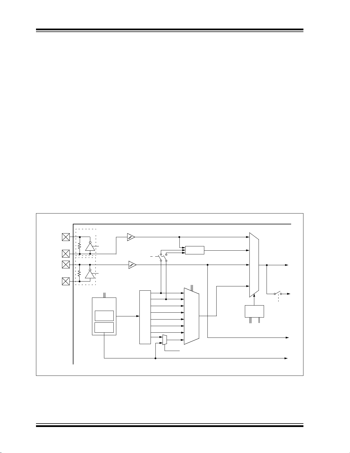
PIC18F2420/2520/4420/4520
4 x PLL
FOSC<3:0>
Secondary Oscillator
T1OSCEN
Enable
Oscillator
T1OSO
T1OSI
Clock Source Option
for Other Modules
OSC1
OSC2
Sleep
HSPLL, INTOSC/PLL
LP, XT, HS, RC, EC
T1OSC
CPU
Peripherals
IDLEN
Postscaler
MUX
MUX
8 MHz
4 MHz
2 MHz
1 MHz
500 kHz
125 kHz
250 kHz
OSCCON<6:4>
111
110
101
100
011
010
001
000
31 kHz
INTRC
Source
Internal
Oscillator
Block
WDT, PWRT, FSCM
8 MHz
Internal Oscillator
(INTOSC)
OSCCON<6:4>
Clock
Control
OSCCON<1:0>
Source
8 MHz
31 kHz (INTRC)
OSCTUNE<6>
0
1
OSCTUNE<7>
and Two-Speed Start-up
Primary Oscillator
PIC18F2420/2520/4420/4520
2.7 Clock Sources and Oscillator Switching
Like previous PIC18 devices, the PIC18F2420/2520/
4420/4520 family includes a feature that allows the
device clock source to be switched from the main oscillator to an alternate low-frequency clock source.
PIC18F2420/2520/4420/4520 devices offer two alternate
clock sources. When an alternate clock source is enabled,
the various power-managed operating modes are
available.
Essentially, there are three clock sources for these
devices:
• Primary oscillators
• Secondary oscillators
• Internal oscillator block
The primary oscillators include the External Crystal
and Resonator modes, the External RC modes, the
External Clock modes and the internal oscillator block.
The particular mode is defined by the FOSC<3:0> Configuration bits. The details of these modes are covered
earlier in this chapter.
The s econdary oscillators are those external sources
not connected to the OSC1 or OSC2 pins. These
sources may continue to operate even after the
controller is placed in a power-managed mode.
PIC18F2420/2520/4420/4520 devices offer the Timer1
oscillator as a secondary oscillator. This oscillator, in all
power-managed modes, is often the time base for
functions such as a Real-Time Clock (RTC).
Most often, a 32.768 kHz watch crystal is connected
between the RC0/T1OSO/T13CKI and RC1/T1OSI
pins. Like the LP Oscillator mode circuit, loading
capacitors are also connected from each pin to ground.
The Timer1 oscillator is discussed in greater detail in
Section 12.3 “Timer1 Oscillator”.
In addition to being a primary clock source, the internal
oscillator block is available as a power-managed
mode clock source. The INTRC source is also used as
the clock source for several special features, such as
the WDT and Fail-Safe Clock Monitor.
The clock sources for the PIC18F2420/2520/4420/4520
devices are shown in Figure 2-8. See Section 23.0
“Special Features of the CPU” for Configuration
register details.
FIGURE 2-8: PIC18F2420/252 0/ 442 0/ 452 0 CL OCK D IA GRA M
DS39631E-page 28 © 2008 Microchip Technology Inc.
 Loading...