


M
PIC18FXX2
Data Sheet
High Performance, Enhanced FLASH
Microcontrollers with 10-Bit A/D
2002 Microchip Technology Inc. DS39564B

Note the following details of the code protection feature on PICmicro® MCUs.
• The PICmicro family meets the specifications contained in the Microchip Data Sheet.
• Microchip believes that its family of PICmicro microcontrollers is one of the most secure products of its kind on the market today,
when used in the intended manner and under normal conditions.
• There are dishonest and possibly illegal methods used to breach the code protection feature. All of these methods, to our knowledge, require using the PICmicro microcontroller in a manner outside the operating specifications contained in the data sheet.
The person doing so may be engaged in theft of intellectual property.
• Microchip is willing to work with the customer who is concerned about the integrity of their code.
• Neither Microchip nor any other semiconductor manufacturer can guarantee the security of their code. Code protection does not
mean that we are guaranteeing the product as “unbreakable”.
• Code protection is constantly evolving. We at Microchip are committed to continuously improving the code protection features of
our product.
If you have any further questions about this matter, please contact the local sales office nearest to you.
Information contained in this publication regarding device
applications and the like is intended through suggestion only
and may be superseded by updates. It is your responsibility to
ensure that your application meets with your specifications.
No representation or warranty is given and no liability is
assumed by Microchip Technology Incorporated with respect
to the accuracy or use of such information, or infringement of
patents or other intellectual property rights arising from such
use or otherwise. Use of Microchip’s products as critical components in life support systems is not authorized except with
express written approval by Microchip. No licenses are conveyed, implicitly or otherwise, under any intellectual property
rights.
Trademarks
The Microchip name and logo, the Microchip logo, K
EELOQ,
MPLAB, PIC, PICmicro, PICSTART and PRO MATE are
registered trademarks of Microchip Technology Incorporated
in the U.S.A. and other countries.
FilterLab, microID, MXDEV, MXLAB, PICMASTER, SEEVAL
and The Embedded Control Solutions Company are
registered trademarks of Microchip Technology Incorporated
in the U.S.A.
dsPIC, dsPICDEM.net, ECONOMONITOR, FanSense,
FlexROM, fuzzyLAB, In-Circuit Serial Programming, ICSP,
ICEPIC, microPort, Migratable Memory, MPASM, MPLIB,
MPLINK, MPSIM, PICC, PICDEM, PICDEM.net, rfPIC, Select
Mode and Total Endurance are trademarks of Microchip
Technology Incorporated in the U.S.A. and other countries.
Serialized Quick Turn Programming (SQTP) is a service mark
of Microchip Technology Incorporated in the U.S.A.
All other trademarks mentioned herein are property of their
respective companies.
© 2002, Microchip Technology Incorporated, Printed in the
U.S.A., All Rights Reserved.
Printed on recycled paper.
Microchip received QS-9000 quality system
certification for its worldwide headquarters,
design and wafer fabrication facilities in
Chandler and Tempe, Arizona in July 1999
and Mountain View, California in March 2002.
The Company’s quality system processes and
procedures are QS-9000 compliant for its
PICmicro
devices, Serial EEPROMs, microperipherals,
non-volatile memory and analog products. In
addition, Microchip’s quality system for the
design and manufacture of development
systems is ISO 9001 certified.
®
8-bit MCUs, KEELOQ
®
code hoppin g
DS39564B - page ii 2002 Microchip Technology Inc.

M
28/40-pin High Performance, Enhanced FLASH
Microcontrollers with 10-Bit A/D
PIC18FXX2
High Performance RISC CPU:
• C compiler optimized architecture/instruction set
- Source code compatible with the PIC16 and
PIC17 instruction sets
• Linear program memory addressing to 32 Kbytes
• Linear data memory addressi ng to 1.5 Kbytes
On-Chip Program
Device
PIC18F242 16K 8192 768 256
PIC18F252 32K 16384 1536 256
PIC18F442 16K 8192 768 256
PIC18F452 32K 16384 1536 256
• Up to 10 MIPs operation:
- DC - 40 MHz osc./clock input
- 4 MHz - 10 MHz osc./clock input with PLL active
• 16-bit wide instructions, 8-bit wide data path
• Priority levels for interrupts
• 8 x 8 Single Cycle Hardware Multiplier
FLASH
(bytes)
Memory
# Single Word
Instructions
On-Chip
RAM
(bytes)
Data
EEPROM
(bytes)
Peripheral Features:
• High current sink/source 25 mA/25 mA
• Three external interrupt pins
• Timer0 module: 8-bit/16-bit timer/counter with
8-bit programmable prescaler
• Timer1 module: 16-bit timer/counter
• Timer2 module: 8-bit timer/counter with 8-bit
period register (time-base for PWM)
• Timer3 module: 16-bit timer/counter
• Secondary oscillator clock option - Timer1/Timer3
• Two Capture/Compare/PWM (CCP) modu les.
CCP pins that can be configured as:
- Capture input: capture is 16-bit,
max. resolution 6.25 ns (T
- Compare is 16-bit, max. resolution 100 ns (T
- PWM output: PWM resolution is 1- to 10-bit,
max. PWM freq. @: 8-bit resolution = 156 kHz
• Master Synchronous Serial Port (MSSP) module,
Two modes of operation:
- 3-wire SPI™ (supports all 4 SPI modes)
2
-I
C™ Master and Slave mode
CY/16)
CY)
10-bit resolution = 39 kHz
Peripheral Features (Continued):
• Addressable USART module:
- Supports RS-485 and RS-232
• Parallel Slave Port (PSP) module
Analog Features:
• Compatible 10-bit Analog-to-D igital Converter
module (A/D) with:
- Fast sampling rate
- Conversion available during SLEEP
-Linearity ≤ 1 LSb
• Programmable Low Voltage Detection (PLVD)
- Supports interrupt on-Low Voltage Dete ct ion
• Programmable Brown-out Reset (BOR)
Special Microcontroller Features:
• 100,000 erase/write cycl e Enhan ced FLASH
program memory typical
• 1,000,000 erase/write cycle Data EEPROM
memory
• FLASH/Data EEPROM Retention: > 40 years
• Self-reprogrammable under software control
• Power-on Reset (POR), Power-up Timer (PWR T)
and Oscillator Start-up Timer (OST)
• Watchdog Timer (WDT) with its own On-Chip RC
Oscillator for reliable operation
• Programmable code protection
• Power saving SLEEP mode
• Selectable oscillator options including:
- 4X Phase Lock Loop (of primary oscillator)
- Secondary Oscillator (32 kHz) clock input
• Single supply 5V In-Ci rcu it Se ria l Pro gram m ing ™
(ICSP™) via two pins
• In-Circuit Debug (ICD) via two pins
CMOS Technology:
• Low power, high speed FLASH/EEPROM
technology
• Fully static design
• Wide operating voltage range (2.0V to 5.5V)
• Industrial and Extended temperature ranges
• Low power consumption:
- < 1.6 mA typical @ 5V, 4 MHz
-25 µA typical @ 3V, 32 kHz
- < 0.2 µA typical standby curr ent
2002 Microchip Technology Inc. DS39564B-page 1

PIC18FXX2
Pin Diagrams
PLCC
REF-
/VPP
RA4/T0CKI
RA5/AN4/SS
OSC2/CLKO/RA6
RC0/T1OSO/T1CKI
/LVDIN
RE0/RD
RE1/WR
RE2/CS
OSC1/CLKI
/AN5
/AN6
/AN7
V
V
DD
SS
NC
RA3/AN3/VREF+
RA2/AN2/V
RA1/AN1
RA0/AN0
MCLR
65432
7
8
9
10
PIC18F442
11
12
PIC18F452
13
14
15
16
181920212223242526
17
RD2/PSP2
RD1/PSP1
RD0/PSP0
RC3/SCK/SCL
RC2/CCP1
RC1/T1OSI/CCP2
*
RC6/TX/CK
RC5/SDO
RC4/SDI/SDA
RD3/PSP3
RD2/PSP2
RD1/PSP1
RD0/PSP0
NC
RB7/PGD
1
44
RC4/SDI/SDA
RD3/PSP3
RC3/SCK/SCL
RB6/PGC
RB5/PGM
42
43
RC5/SDO
RC2/CCP1
RC1/T1OSI/CCP2*NC
RB4
41
27
28
NC
RC6/TX/CK
NC
40
39
38
37
36
35
34
33
32
31
30
29
RB3/CCP2*
RB2/INT2
RB1/INT1
RB0/INT0
V
DD
VSS
RD7/PSP7
RD6/PSP6
RD5/PSP5
RD4/PSP4
RC7/RX/DT
TQFP
RC7/RX/DT
RD4/PSP4
RD5/PSP5
RD6/PSP6
RD7/PSP7
SS
V
VDD
RB0/INT0
RB1/INT1
RB2/INT2
RB3/CCP2
* RB3 is the alternate pin for the CCP2 pin multiplexing.
*
4443424140
1
2
3
4
PIC18F442
5
6
PIC18F452
7
8
9
10
121314
11
NC
RB4
NC
15
16
RB6/PGC
RB5/PGM
38
39
37
1819202122
17
RA0/AN0
MCLR
RB7/PGD
/VPP
363435
RA1/AN1
33
32
31
30
29
28
27
26
25
24
23
RA2/AN2/V
RA3/AN3/VREF+
REF-
NC
RC0/T1OSO/T1CKI
OSC2/CLKO/RA6
OSC1/CLKI
SS
V
VDD
RE2/AN7/CS
RE1/AN6/WR
RE0/AN5/RD
RA5/AN4/SS/LVDIN
RA4/T0CKI
DS39564B-page 2 2002 Microchip Technology Inc.

Pin Diagrams (Cont.’d)
PIC18FXX2
DIP
Note: Pin compatible with 40-pin PIC16C7X devices.
MCLR/VPP
RA0/AN0
RA1/AN1
RA2/AN2/V
RA3/AN3/V
RA5/AN4/SS
OSC2/CLKO/RA6
RC0/T1OSO/T1CKI
RC1/T1OSI/CCP2
RC3/SCK/SCL
RA4/T0CKI
/LVDIN
RE0/RD
RE1/WR
RE2/CS
OSC1/CLKI
RC2/CCP1
RD0/PSP0
RD1/PSP1
REF-
REF+
/AN5
/AN6
/AN7
V
VSS
DD
1
2
3
4
5
6
7
8
9
10
11
12
13
14
*
15
16
17
18
19
20
40
39
38
37
36
35
34
33
32
31
30
PIC18F442
29
PIC18F452
28
27
26
25
24
23
22
21
RB7/PGD
RB6/PGC
RB5/PGM
RB4
RB3/CCP2
RB2/INT2
RB1/INT1
RB0/INT0
V
DD
VSS
RD7/PSP7
RD6/PSP6
RD5/PSP5
RD4/PSP4
RC7/RX/DT
RC6/TX/CK
RC5/SDO
RC4/SDI/SDA
RD3/PSP3
RD2/PSP2
*
DIP, SOIC
MCLR/VPP
RA0/AN0
RA1/AN1
RA2/AN2/V
RA3/AN3/V
RA5/AN4/SS
OSC2/CLKO/RA6
RC0/T1OSO/T1CKI
RC1/T1OSI/CCP2
RC3/SCK/SCL
* RB3 is the alternate pin for the CCP2 pin multiplexing.
REF-
REF+
RA4/T0CKI
/LVDIN
V
OSC1/CLKI
RC2/CCP1
SS
10
*
11
12
13
14
1
2
3
4
5
6
7
8
9
PIC18F242
28
27
26
25
24
23
22
21
20
19
PIC18F252
18
17
16
15
RB7/PGD
RB6/PGC
RB5/PGM
RB4
RB3/CCP2
RB2/INT2
RB1/INT1
RB0/INT0
V
VSS
RC7/RX/DT
RC6/TX/CK
RC5/SDO
RC4/SDI/SDA
*
DD
2002 Microchip Technology Inc. DS39564B-page 3

PIC18FXX2
Table of Contents
1.0 Device Overview..........................................................................................................................................................................7
2.0 Oscillator Configurations............................................................................................................................................................ 17
3.0 Reset..........................................................................................................................................................................................25
4.0 Memory Organization.................................................................................................................................................................35
5.0 FLASH Program Memory......................................................................... .................................................................................. 55
6.0 Data EEPROM Memory.............................................................................................................................................................65
7.0 8 X 8 Hardware Multiplier.......................................................................................... ................................................................. 71
8.0 Interrupts....................................................................................................................................................................................73
9.0 I/O Ports............................................. .................................................. ......................................................................................87
10.0 Timer0 Module ......................................................................................................................................................................... 103
11.0 Timer1 Module ......................................................................................................................................................................... 107
12.0 Timer2 Module ......................................................................................................................................................................... 111
13.0 Timer3 Module ......................................................................................................................................................................... 113
14.0 Capture/Compare/PWM (CCP) Modules ... ...... ............. ...... .... ............. ...... ............. .... ...... ............. ..........................................117
15.0 Master Synchronous Serial Port (MSSP) Module ....................................................................................................................125
16.0 Addressable Universal Synchronous Asynchronous Receiv er Transmitter (USA RT)..............................................................165
17.0 Compatible 10-bit Analog-to-Digital Converter (A/D) Module...................................................................................................181
18.0 Low Voltage Detect ..................................................................................................................................................................189
19.0 Special Features of the CPU....................................................................................................................................................195
20.0 Instruction Set Summary..........................................................................................................................................................211
21.0 Development Support............................................................................................................................................................... 253
22.0 Electrical Characteristics..........................................................................................................................................................259
23.0 DC and AC Characteristics Graphs and Tables.......................................................................................................................289
24.0 Packaging Information..... ......................................................................................................................................................... 305
Appendix A: Revision History............................................................................................................................................................ 313
Appendix B: Device Differences........................................................................................................................................................313
Appendix C: Conversion Considerations.................................................................... .. .... .. .. .... .. ....................................................... 314
Appendix D: Migration from Baseline to Enhanced Devices ................................................................. .... ........................................314
Appendix E: Migration from Mid-range to Enhanced Devices........................................................................................................... 315
Appendix F: Migration from High-end to Enhanced Devices ............................................................................................................ 315
Index ..................................................................................................................................................................................................317
On-Line Support........................................................................ .. .... ......... .. .... .... .. ......... .. ................................................................... 327
Reader Response..............................................................................................................................................................................328
PIC18FXX2 Product Identification System......................................................................................................................................... 329
DS39564B-page 4 2002 Microchip Technology Inc.

PIC18FXX2
TO OUR VALUED CUSTOMERS
It is our intention to provide our valued customers with the best documentation possible to ensure successful use of your Microchip
products. To this end, we will continue to improve our publications to better suit your needs. Our publications will be refined and
enhanced as new volumes and updates are introduced.
If you have any questions or c omm ents regarding th is publication, p lease c ontact the M a rketing Communications Department via
E-mail at docerrors@mail.microchip.com or fax the Reader Response Form in the back of this data sheet to (480) 792-4150.
We welcome your feedback.
Most Current Data Sheet
To obtain the most up-to-date version of this data sheet, please register at our Worldwide Web site at:
http://www.microchip.com
You can determine the version of a data sheet by examining its literature number found on the bottom outside corner of any page.
The last character of the literature number is the version number, (e.g., DS30000A is version A of document DS30000).
Errata
An errata sheet, describing minor operational differences from the data sheet and recommended workarounds, may exist for current
devices. As device/documentation issues become known to us, we will publish an errata sheet. The errata will specify the revision
of silicon and revision of document to which it applies.
To determine if an errata sheet exists for a particular device, please check with one of the following:
• Microchip’s Worldwide Web site; http://www.microchip.com
• Your local Microchip sales office (see last page)
• The Microchip Corporate Literature Center; U.S. FAX: (480) 792-7277
When contacting a sales office or the literature center, please specify which device, revision of silicon and data sheet (include literature number) you are using.
Customer Notification System
Register on our web site at www.microchip.com/cn to receive the most current information on all of our products.
2002 Microchip Technology Inc. DS39564B-page 5

PIC18FXX2
NOTES:
DS39564B-page 6 2002 Microchip Technology Inc.

PIC18FXX2
1.0 DEVICE OVERVIEW
This documen t conta i ns dev ic e spec if i c in for m at i on fo r
the following devices:
• PIC18F242 • PIC18F442
• PIC18F252 • PIC18F452
These devices com e in 28-pin and 40/44-pin pac kages.
The 28-pin devices do not have a Parallel Slave Port
(PSP) implemented and the number of Analog-toDigital (A/D) converter input channels is reduced to 5.
An overview of features is shown in Table 1-1.
The following two figures are device block diagrams
sorted by pin count: 28-p in for Figure 1-1 and 40/44-pin
for Figure 1-2. The 28-pin and 40/44-pin pinouts are
listed in Table 1-2 and Table 1-3, respectively.
TABLE 1-1: DEVICE FEATURES
Features PIC18F242 PIC18F252 PIC18F442 PIC18F452
Operating Frequency DC - 40 MHz DC - 40 MHz DC - 40 MHz DC - 40 MHz
Program Memory (Bytes) 16K 32K 16K 3 2K
Program Memory (Instruction s) 8192 16384 8192 16 384
Data Memory (Bytes) 768 1536 768 15 36
Data EEPROM Memory (Bytes) 256 256 256 256
Interrupt Sources 17 17 18 18
I/O Ports Ports A, B, C Ports A, B, C Ports A, B, C, D, E Ports A, B, C, D, E
Timers 4 4 4 4
Capture/Compare/PWM Modules 2 2 2 2
MSSP,
Serial Communications
Parallel Communications ——PSP PSP
10-bit Analog-to-Digital Module 5 input channels 5 input channels 8 input channels 8 input channels
RESETS (and Delays)
Programmable Low Voltage
Detect
Programmable Brown-out Reset Yes Yes Yes Yes
Instruction Set 75 Instructions 75 Instructions 75 Instructions 75 Instructions
Packages
Addressable
USART
POR, BOR,
RESET Instruction,
Stack Full,
Stack Underflow
(PWRT, OST)
Yes Yes Yes Yes
28-pin DIP
28-pin SOIC
MSSP,
Addressable
USART
POR, BOR,
RESET Instruction,
Stack Full,
Stac k U nde rflo w
(PWRT, OST)
28-pin DIP
28-pin SOIC
MSSP,
Addressable
USART
POR, BOR,
RESET Instruction,
Stack Full,
Stac k Un de rflo w
(PWRT, OST)
40-pin DIP
44-pin PLCC
44-pin TQFP
MSSP,
Addressable
USART
POR, BOR,
RESET Instruction,
Stack Full,
Stac k U nde rflo w
(PWRT, OST)
40-pin DIP
44-pin PLCC
44-pin TQFP
2002 Microchip Technology Inc. DS39564B-page 7

PIC18FXX2
FIGURE 1-1: PIC18F2X2 BLOCK DIAGRAM
Data Bus<8>
Address Latch
Program Memory
(up to 2 Mbytes)
Data Latch
OSC2/CLKO
OSC1/CLKI
T1OSCI
T1OSCO
MCLR
VDD, VSS
Table Pointer
21
8
21
inc/dec logic
21
PCLATH
PCLATU
PCH
PCU
Program Counter
31 Level Stack
16
Table Latch
8
ROM Latch
8
8
PCL
4
Decode
BSR
Data Latch
Data RAM
Address Latch
12
Address<12>
12 4
FSR0
FSR1
FSR2
inc/dec
logic
(2)
Bank0, F
12
PORTA
PORTB
RA0/AN0
RA1/AN1
RA2/AN2/VREFRA3/AN3/VREF+
RA4/T0CKI
RA5/AN4/SS
RA6
/LVDIN
RB0/INT0
RB1/INT1
RB2/INT2
RB3/CCP2
(1)
RB4
RB5/PGM
RB6/PCG
RB7/PGD
RC0/T1OSO/T1CKI
RC1/T1OSI/CCP2
RC2/CCP1
RC3/SCK/SCL
RC4/SDI/SDA
RC5/SDO
RC6/TX/CK
RC7/RX/DT
(1)
Instruction
Decode &
Control
Timing
Generation
4X PLL
Precision
Voltage
Reference
Instruction
Register
Power-up
Timer
Oscillator
Start-up Timer
Power-on
Reset
Watchdog
Timer
Brown-out
Reset
Low Voltage
Programming
In-Circuit
Debugger
BIT OP
3
8
8 x 8 Multiply
WREG
8
8
ALU<8>
8
PRODLPRODH
8
8
PORTC
8
Timer0 Timer1 Timer2
Master
CCP1
CCP2
Synchronous
Serial Port
Timer3
Addressable
USART
A/D Converter
Data EEPROM
Note 1: Optional multiplexing of CCP2 input/output with RB3 is enabled by selection of configuration bit.
2: The high order bits of the Direct Address for the RAM are from the BSR register (except for the
3: Many o f th e general purpose I/O p i ns a re m ultipl e xed wi th on e or mo re peripheral module functions. The multi p lexing combinations
are device dependent.
MOVFF instruction).
DS39564B-page 8 2002 Microchip Technology Inc.

FIGURE 1-2: PIC18F4X2 BLOCK DIAGRAM
Table Pointer
Address Latch
Program Memory
(up to 2 Mbytes)
Data Latch
OSC2/CLKO
OSC1/CLKI
T1OSCI
T1OSCO
MCLR
VDD, VSS
21
8
21
16
inc/dec logic
Table Latch
Instruction
Decode &
Control
Timing
Generation
4X PLL
Precision
Voltage
Reference
21
8
PCLATU
PCLATH
PCH PCL
PCU
Program Counter
31 Level Stack
ROM Latch
Instruction
Register
Power-up
Timer
Oscillator
Start-up Timer
Power-on
Reset
Watchdog
Timer
Brown-out
Reset
Low Voltage
Programming
In-Circuit
Debugger
8
8
address reach)
12 4
4
BSR
Decode
BIT OP
inc/dec
3
8
Data Bus<8>
Data Latch
Data RA M
(up to 4K
Address Latc h
12
Address<12>
Bank0, F
FSR0
FSR1
FSR2
logic
PRODLPRODH
8 x 8 Multiply
WREG
8
8
ALU<8>
8
PIC18FXX2
PORTA
(2)
PORTB
12
PORTC
8
8
8
PORTD
PORTE
RA0/AN0
RA1/AN1
RA2/AN2/VREF-
RA3/AN3/VREF+
RA4/T0CKI
RA5/AN4/SS
RA6
RB0/INT0
RB1/INT1
RB2/INT2
RB3/CCP2
RB4
RB5/PGM
RB6/PCG
RB7/PGD
RC0/T1OSO/T1CKI
RC1/T1OSI/CCP2
RC2/CCP1
RC3/SCK/SCL
RC4/SDI/SDA
RC5/SDO
RC6/TX/CK
RC7/RX/DT
RD0/PSP0
RD1/PSP1
RD2/PSP2
RD3/PSP3
RD4/PSP4
RD5/PSP5
RD6/PSP6
RD7/PSP7
RE0/AN5/RD
RE1/AN6/WR
RE2/AN7/CS
/LVDIN
(1)
(1)
Timer0
CCP1
Note 1: Optional multiplexing of CCP2 input/output with RB3 is enabled by selection of configuration bit.
2: The high order bits of the Direct Address for the RAM are from the BSR register (except for the
3: Many of the general purpose I/O pins are multiplexed with one or more peripheral module functions. The multiplexing combinations
are device dependent.
Timer1 Timer2
Master
CCP2
Synchronous
Serial Port
Timer3
Addressable
USART
Parallel Slave Port
MOVFF instruction).
A/D Converter
Data EEPROM
2002 Microchip Technology Inc. DS39564B-page 9

PIC18FXX2
TABLE 1-2: PIC18F2X2 PINOUT I/O DESCRIPTIONS
Pin Name
MCLR/VPP
MCLR
VPP
NC ——— —These pins should be left unconnected.
OSC1/CLKI
OSC1
CLKI
OSC2/CLKO/RA6
OSC2
CLKO
RA6
RA0/AN0
RA0
AN0
RA1/AN1
RA1
AN1
RA2/AN2/V
RA2
AN2
V
RA3/AN3/V
RA3
AN3
V
RA4/T0CKI
RA4
T0CKI
RA5/AN4/SS
RA5
AN4
SS
LVDIN
RA6 See the OSC2/CLKO/RA6 pin.
Legend: TTL = TTL compatible input CMOS = CMOS compatible input or output
REF-
REF-
REF+
REF+
/LVDIN
ST = Schmitt Trigger input with CMOS levels I = Input
O = Output P = Power
OD = Open Drain (no P diode to V
Pin Number
DIP SOIC
11
99
10 10
22
33
44
55
66
77
Pin
Type
Buffer
Type
I
I
I
I
O
O
I/O
I/O
I
I/O
I
I/O
I
I
I/O
I
I
I/OIST/OD
I/O
I
I
I
ST
ST
ST
CMOS
—
—
TTL
TTL
Analog
TTL
Analog
TTL
Analog
Analog
TTL
Analog
Analog
ST
TTL
Analog
ST
Analog
DD)
Description
Master Clear (input) or high voltage ICSP programming
enable pin.
Master Clear (Reset) input. This pin is an active low
RESET to the device.
High voltage ICSP programmi ng ena ble pin.
Oscillator crystal or external clock input.
Oscillator crystal input or external clock source input.
ST buffer when configured in RC mode, CMOS otherwise.
External clock source input. Always associated with
pin function OSC1. (See related OSC1/CLKI,
OSC2/CLKO pins.)
Oscillator crystal or clock output.
Oscillator crystal output. Connects to crystal or
resonator in Crystal Oscillator mode.
In RC mode, OSC2 pin outputs CLKO which has 1/4
the frequency of OSC1, and denotes the instruction
cycle rate.
General Purpose I/O pin.
PORTA is a bi-directional I/O port.
Digital I/O.
Analog input 0.
Digital I/O.
Analog input 1.
Digital I/O.
Analog input 2.
A/D Reference Voltage (Low) input.
Digital I/O.
Analog input 3.
A/D Reference Voltage (High) input.
Digital I/O. Open drain when configured as output.
Timer0 external clock input.
Digital I/O.
Analog input 4.
SPI Slave S elect input.
Low Voltage Detect Input.
DS39564B-page 10 2002 Microchip Technology Inc.
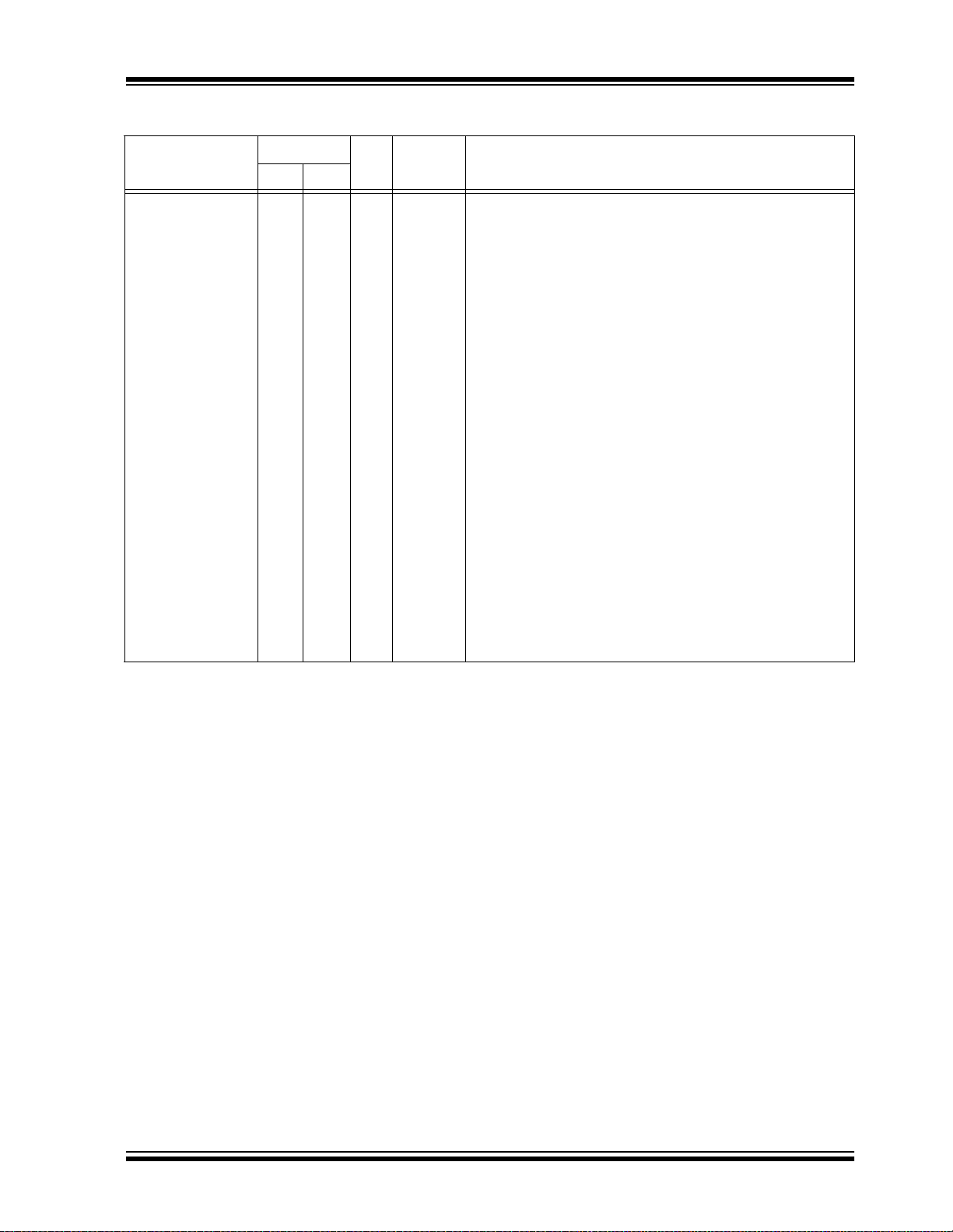
TABLE 1-2: PIC18F2X2 PINOUT I/O DESCRIPTIONS (CONTINUED)
PIC18FXX2
Pin Name
RB0/INT0
RB0
INT0
RB1/INT1
RB1
INT1
RB2/INT2
RB2
INT2
RB3/CCP2
RB3
CCP2
RB4 25 25 I/O TTL Digital I/O.
RB5/PGM
RB5
PGM
RB6/PGC
RB6
PGC
RB7/PGD
RB7
PGD
Legend: TTL = TTL compatible input CMOS = CMOS compatible input or output
ST = Schmitt Trigger input with CMOS levels I = Input
O = Output P = Power
OD = Open Drain (no P diode to V
Pin Number
DIP SOIC
21 21
22 22
23 23
24 24
26 26
27 27
28 28
Pin
Type
I/O
I
I/O
I
I/O
I
I/O
I/O
I/O
I/O
I/O
I/O
I/O
I/O
Buffer
Type
PORTB is a bi-directional I/O port. PORTB can be software
programmed for internal weak pull-ups on all inputs.
TTL
ST
TTL
ST External Interrupt 1.
TTL
ST
TTL
ST
TTL
ST
TTL
ST
TTL
ST
DD)
Digital I/O.
External Interrupt 0.
Digital I/O.
External Interrupt 2.
Digital I/O.
Capture2 input, Compare2 output, PWM2 output.
Interrupt-on-change pin.
Digital I/O. Interrupt-on-change pin.
Low Voltage ICSP programming enable pin.
Digital I/O. Interrupt-on-change pin.
In-Circuit Debugger and ICSP programming clock pin.
Digital I/O. Interrupt-on-change pin.
In-Circuit Debugger and ICSP programming data pin.
Description
2002 Microchip Technology Inc. DS39564B-page 11
PIC18FXX2
TABLE 1-2: PIC18F2X2 PINOUT I/O DESCRIPTIONS (CONTINUED)
Pin Name
RC0/T1OSO/T1CKI
RC0
T1OSO
T1CKI
RC1/T1OSI/CCP2
RC1
T1OSI
CCP2
RC2/CCP1
RC2
CCP1
RC3/SCK/SCL
RC3
SCK
SCL
RC4/SDI/SDA
RC4
SDI
SDA
RC5/SDO
RC5
SDO
RC6/TX/CK
RC6
TX
CK
RC7/RX/DT
RC7
RX
DT
SS 8, 19 8, 19 P — Ground reference for logic and I/O pins.
V
VDD 20 20 P — Positive supply for logic and I/O pins.
Legend: TTL = TTL compatible input CMOS = CMOS compatible input or output
ST = Schmitt Trigger input with CMOS levels I = Input
O = Output P = Power
OD = Open Drain (no P diode to V
Pin Number
DIP SOIC
11 11
12 12
13 13
14 14
15 15
16 16
17 17
18 18
Pin
Type
I/O
O
I
I/O
I
I/O
I/O
I/O
I/O
I/O
I/O
I/O
I
I/O
I/O
O
I/O
O
I/O
I/O
I
I/O
Buffer
Type
CMOS
DD)
ST
—
ST
ST
ST
ST
ST
ST
ST
ST
ST
ST
ST
ST
—
ST
—
ST
ST
ST
ST
Description
PORTC is a bi-directional I/O port.
Digital I/O.
Timer1 oscillator output.
Timer1/Timer3 external clock input.
Digital I/O.
Timer1 oscillator input.
Capture2 input, Compare2 output, PWM2 output.
Digital I/O.
Capture1 input/Compare1 output/PWM1 output.
Digital I/O.
Synchronous serial clock input/output for SPI mode.
Synchronous serial clock input/output for I
Digital I/O.
SPI Data In.
2
C Data I/O.
I
Digital I/O.
SPI Data Out.
Digital I/O.
USART Asynchronous Transmit.
USART Synchronous Clock (see related RX/DT).
Digital I/O.
USART Asynchronous Receive.
USART Synchronous Data (see related TX/CK).
2
C mode
DS39564B-page 12 2002 Microchip Technology Inc.

TABLE 1-3: PIC18F4X2 PINOUT I/O DESCRIPTIONS
PIC18FXX2
Pin Name
/VPP
MCLR
MCLR
VPP
NC ———These pins should be left unconnected.
OSC1/CLKI
OSC1
CLKI
OSC2/CLKO/RA6
OSC2
CLKO
RA6
RA0/AN0
RA0
AN0
RA1/AN1
RA1
AN1
RA2/AN2/V
RA2
AN2
V
RA3/AN3/VREF+
RA3
AN3
V
RA4/T0CKI
RA4
T0CKI
RA5/AN4/SS/LVDIN
RA5
AN4
SS
LVDIN
RA6 (See the OSC2/CLKO/RA6 pin.)
Legend: TTL = TTL compatible input CMOS = CMOS compatible input or output
REF-
REF-
REF+
ST = Schmitt Trigger input with CMOS levels I = Input
O = Output P = Power
OD = Open Drain (no P diode to V
Pin Number
DIP PLCC TQFP
1218
13 14 30
14 15 31
2319
3420
4521
5622
6723
7824
Pin
Type
I
I
I
I
O
O
I/O
I/O
I
I/O
I
I/O
I
I
I/O
I
I
I/OIST/OD
I/O
I
I
I
DD)
Buffer
Type
ST
ST
ST
CMOS
—
—
TTL
TTL
Analog
TTL
Analog
TTL
Analog
Analog
TTL
Analog
Analog
ST
TTL
Analog
ST
Analog
Description
Master Clear (input) or high voltage ICSP
programming enable pin.
Master Clear (Reset) input. This pin is an active
low RESET to the device.
High voltage ICSP programming enable pin.
Oscillator crystal or external clock input.
Oscillator crystal input or external clock source
input. ST buffer when configured in RC mode,
CMOS otherwise.
External clock source input. Always associated
with pin function OSC1. (See rel ate d O SC1/C LKI ,
OSC2/CLKO pins.)
Oscillator crystal or clock output.
Oscillator crystal output. Connects to crystal
or resonator in Crystal Oscillator mode.
In RC mode, OSC2 pin outputs CLKO,
which has 1/4 the frequency of OSC1 and
denotes the instruction cy cl e rate.
General Pur pose I/O pin.
PORTA is a bi-directional I/O port.
Digital I/O.
Analog input 0.
Digital I/O.
Analog input 1.
Digital I/O.
Analog input 2.
A/D Reference Voltage (Low) input.
Digital I/O.
Analog input 3.
A/D Reference Voltage (High) input.
Digital I/O. Open drain when configured as output.
Timer0 external clock input.
Digital I/O.
Analog input 4.
SPI Slave Select input.
Low Voltage Detect Input.
2002 Microchip Technology Inc. DS39564B-page 13

PIC18FXX2
TABLE 1-3: PIC18F4X2 PINOUT I/O DESCRIPTIONS (CONTINUED)
Pin Name
RB0/INT0
RB0
INT0
RB1/INT1
RB1
INT1
RB2/INT2
RB2
INT2
RB3/CCP2
RB3
CCP2
RB4 37 41 14 I/O TTL Digital I/O. Interrupt-on-change pin.
RB5/PGM
RB5
PGM
RB6/PGC
RB6
PGC
RB7/PGD
RB7
PGD
Legend: TTL = TTL compatible input CMOS = CMOS compatible input or output
ST = Schmitt Trigger input with CMOS levels I = Input
O = Output P = Power
OD = Open Drain (no P diode to V
Pin Number
DIP PLCC TQFP
33 36 8
34 37 9
35 38 10
36 39 11
38 42 15
39 43 16
40 44 17
Type
DD)
Pin
I/O
I
I/O
I
I/O
I
I/O
I/O
I/O
I/O
I/O
I/O
I/O
I/O
Buffer
Type
PORTB is a bi-directional I/O port. PORTB can be
software programmed fo r internal weak pull-up s on all
inputs.
TTL
ST
TTL
ST External Interrupt 1.
TTL
ST
TTL
ST
TTL
ST
TTL
ST
TTL
ST
Digital I/O.
External Interrupt 0.
Digital I/O.
External Interrupt 2.
Digital I/O.
Capture2 input, Compare2 output, PWM2 output.
Digital I/O. Interrupt-on-change pin.
Low Voltage ICSP programming enable pin.
Digital I/O. Interrupt-on-change pin.
In-Circuit Debugger and ICSP programming clock
pin.
Digital I/O. Interrupt-on-change pin.
In-Circuit Debugger and ICSP programming data
pin.
Description
DS39564B-page 14 2002 Microchip Technology Inc.

TABLE 1-3: PIC18F4X2 PINOUT I/O DESCRIPTIONS (CONTINUED)
PIC18FXX2
Pin Name
RC0/T1OSO/T1CKI
RC0
T1OSO
T1CKI
RC1/T1OSI/CCP2
RC1
T1OSI
CCP2
RC2/CCP1
RC2
CCP1
RC3/SCK/SCL
RC3
SCK
SCL
RC4/SDI/SDA
RC4
SDI
SDA
RC5/SDO
RC5
SDO
RC6/TX/CK
RC6
TX
CK
RC7/RX/DT
RC7
RX
DT
Legend: TTL = TTL compatible input CMOS = CMOS compatible input or output
ST = Schmitt Trigger input with CMOS levels I = Input
O = Output P = Power
OD = Open Drain (no P diode to V
Pin Number
DIP PLCC TQFP
15 16 32
16 18 35
17 19 36
18 20 37
23 25 42
24 26 43
25 27 44
26 29 1
Type
DD)
Pin
I/O
O
I
I/O
I
I/O
I/O
I/O
I/O
I/O
I/O
I/O
I
I/O
I/O
O
I/O
O
I/O
I/O
I
I/O
Buffer
Type
ST
—
ST
ST
CMOS
ST
ST
ST
ST
ST
ST
ST
ST
ST
ST
—
ST
—
ST
ST
ST
ST
Description
PORTC is a bi-directional I/O port.
Digital I/O.
Timer1 oscillator output.
Timer1/Timer3 external clock input.
Digital I/O.
Timer1 oscillator input.
Capture2 input, Compare2 output, PWM2 output.
Digital I/O.
Capture1 input/Compare1 output/PWM1 output.
Digital I/O.
Synchronous serial clock input/output for
SPI mode.
Synchronous serial clock input/output for
2
C mode.
I
Digital I/O.
SPI Data In.
2
C Data I/O.
I
Digital I/O.
SPI Data Out.
Digital I/O.
USART Asynchronous Transmit.
USART Synchronous Cloc k (se e relate d RX/DT ).
Digital I/O.
USART Asynchronous Receive.
USART Synchronous Data (see related TX/CK).
2002 Microchip Technology Inc. DS39564B-page 15

PIC18FXX2
TABLE 1-3: PIC18F4X2 PINOUT I/O DESCRIPTIONS (CONTINUED)
Pin Name
RD0/PSP0 19 21 38 I/O ST
RD1/PSP1 20 22 39 I/O ST
RD2/PSP2 21 23 40 I/O ST
RD3/PSP3 22 24 41 I/O ST
RD4/PSP4 27 30 2 I/O ST
RD5/PSP5 28 31 3 I/O ST
RD6/PSP6 29 32 4 I/O ST
RD7/PSP7 30 33 5 I/O ST
RE0/RD
RE1/WR
RE2/CS
V
V
Legend: TTL = TTL compatible input CMOS = CMOS compatible input or output
/AN5
RE0
RD
AN5
/AN6
RE1
WR
AN6
/AN7
RE2
CS
AN7
SS 12, 31 13, 34 6, 29 P — Ground reference for logic and I/O pins.
DD 11, 32 12, 35 7, 28 P — Positive supply for logic and I/O pins.
ST = Schmitt Trigger input with CMOS levels I = Input
O = Output P = Power
OD = Open Drain (no P diode to V
Pin Number
DIP PLCC TQFP
8 9 25 I/O
9 10 26 I/O
10 11 27 I/O
Type
DD)
Pin
Buffer
Type
TTL
TTL
TTL
TTL
TTL
TTL
TTL
TTL
ST
TTL
Analog
ST
TTL
Analog
ST
TTL
Analog
Description
PORTD is a bi-directio nal I/O po rt, or a Paral le l Slav e
Port (PSP) for interfacing to a microprocessor port.
These pins have TTL i npu t b uffers when PSP modul e
is enabled.
Digital I/O.
Parallel Slave Port Data.
Digital I/O.
Parallel Slave Port Data.
Digital I/O.
Parallel Slave Port Data.
Digital I/O.
Parallel Slave Port Data.
Digital I/O.
Parallel Slave Port Data.
Digital I/O.
Parallel Slave Port Data.
Digital I/O.
Parallel Slave Port Data.
Digital I/O.
Parallel Slave Port Data.
PORTE is a bi-directional I/O port.
Digital I/O.
Read control for parallel slave port
(see also WR
Analog input 5.
Digital I/O.
Write control for parallel slave port
(see CS
Analog input 6.
Digital I/O.
Chip Select control for parallel slave port
(see related RD
Analog input 7.
and CS pins).
and RD pins).
and WR).
DS39564B-page 16 2002 Microchip Technology Inc.

PIC18FXX2
2.0 OSCILLATOR CONFIGURATIONS
2.1 Oscillator Types
The PIC18FXX2 can be operated in eight different
Oscillator modes . The u ser c an prog ram th ree con figuration bits (FOSC2 , FOSC1, and FOSC 0) to sel ect on e
of these eight modes:
1. LP Low Power Crystal
2. XT Crystal/Resonator
3. HS High Speed Crystal/Resonator
4. HS + PLL High Speed Crystal/Resonator
with PLL enabled
5. RC Ex tern al R esi st or/C apacitor
6. RCIO External Resistor/Capacitor with
I/O pin enabled
7. EC External Clock
8. ECIO External Clock with I/O pin
enabled
2.2 Crystal Oscillator/Ceramic Resonators
In XT, LP, HS or HS+PLL Oscillator mod es , a c ry st a l or
ceramic resonator is connected to the OSC1 and
OSC2 pins to establish oscillation. Figure 2-1 shows
the pin connections.
The PIC18FXX2 oscilla tor d esign requires the use of a
parallel cut crystal.
Note: Use of a series cut crystal may give a fre-
quency out of the crystal manufacturers
specifications.
FIGURE 2-1: CRYSTAL/CERAMIC
RESONATOR OPERATION
(HS, XT OR LP
CONFIGURATION)
(1)
C1
C2
(1)
XTAL
(2)
RS
OSC1
OSC2
RF
(3)
To
Internal
Logic
SLEEP
PIC18FXXX
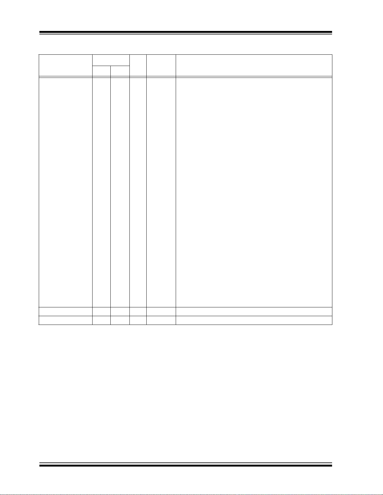
T ABLE 2-1: CAPACITOR SELECTION FOR
CERAMIC RESONATORS
Ranges Tested:
Mode Freq C1 C2
XT 455 kHz
2.0 MHz
4.0 MHz
HS 8.0 MHz
16.0 MHz
68 - 100 pF
15 - 68 pF
15 - 68 pF
10 - 68 pF
10 - 22 pF
68 - 100 pF
15 - 68 pF
15 - 68 pF
10 - 68 pF
10 - 22 pF
These values are for design guid ance only.
See notes following this table.
Resonators Used:
455 kHz Panasonic EFO-A455K04B ± 0.3%
2.0 MHz Murata Erie CSA2.00MG ± 0.5%
4.0 MHz Murata Erie CSA4.00MG ± 0.5%
8.0 MHz Murata Erie CSA8.00MT ± 0.5%
16.0 MHz Murata Erie CSA16.00MX ± 0.5%
All resonators used did not have built-in capacitors.
Note 1: Higher cap acitance increases th e stabi lity
of the oscillator, but also increases the
start-up time.
2: When operating below 3V V
using certain ceramic resonators at any
voltage, it may be necessary to use
high-gain HS mode, tr y a lowe r frequency
resonator, or switch to a crystal oscillator.
3: Since each resonator/crystal has its own
characteristics, the user should consul t the
resonator/crystal manufacturer for appropriate values of external components, or
verify oscillator performance.
DD, or when
Note 1: See Table 2-1 and Table 2-2 for
recommended values of C1 and C2.
2: A series resistor (R
AT strip cut crystals.
F varies with the Oscillator mode chosen.
3: R
2002 Microchip Technology Inc. DS39564B-page 17
S) may be required for

PIC18FXX2
TABLE 2-2: CAPACITOR SELECTION FOR
CRYSTAL OSCILLATOR
Ranges Tested:
Mode Freq C1 C2
LP 32.0 kHz 33 pF 33 pF
200 kHz 15 pF 15 pF
XT 200 kHz 22-68 pF 22-68 pF
1.0 MHz 15 pF 15 pF
4.0 MHz 15 pF 15 pF
HS 4.0 MHz 15 pF 15 pF
8.0 MHz 15-33 pF 15-33 pF
20.0 MHz 15-33 pF 15-33 pF
25.0 MHz 15-33 pF 15-33 pF
These values are for de sign guid ance only.
See notes following this table.
Crystals Used
32.0 kHz Epson C-001R32.768K-A ± 20 PPM
200 kHz STD XTL 200.000KHz ± 20 PPM
1.0 MHz ECS ECS-10-13-1 ± 50 PPM
4.0 MHz ECS ECS-40-20-1 ± 50 PPM
8.0 MHz Epson CA-301 8.000M-C ± 30 PPM
20.0 MHz Epson CA-301 20.000M-C ± 30 PPM
Note 1: Higher capacitanc e increases th e stabi lity
of the oscillator, but also increases the
start-up time.
2: Rs may be required in HS mode, as well
as XT mode, to avoid overdrivi ng crys t als
with low drive level specification.
3: Since each resonator/crystal has its own
characteristics, the user should consult the
resonator/crystal manufacturer for appropriate values of external components., or
verify oscillator performance.
An external clock sourc e may also be conne cted to th e
OSC1 pin in the HS, XT and LP modes, as shown in
Figure 2-2.
2.3 RC Oscillator
For timing-insensitive applications, the “RC” and
“RCIO” device options offer additional cost savings.
The RC oscillator frequency is a function of the supply
voltage, the resistor (R
ues and the operating temperature. In addition to this,
the oscillator frequency will vary from uni t to unit due to
normal process parameter variation. Furthermore, the
difference in le ad fram e c apacitance be tw ee n package
types will also affect the oscillation frequency, especially for low C
EXT values. The user also needs to take
into account variation due to tolerance of external R
and C components used. Figure 2-3 shows how the
R/C combination is connected.
In the RC Oscillator mode, the oscillator frequency
divided by 4 is available on the OSC2 pin. This signal
may be used f or t e st pu r pos es or t o sy nc hr o n iz e ot he r
logic.
Note: If the oscillator frequency divided by 4 sig-
nal is not required in the application, it is
recommended to use RCIO mode to save
current.
FIGURE 2-3: RC OSCILLATOR MODE
VDD
REXT
CEXT
VSS
F
Recommended values:3 kΩ ≤ REXT ≤ 100 kΩ
The RCIO Oscillato r mode f unctio ns li ke t he RC m ode,
except that the OSC2 pin becomes an additional general purpose I/O pin. The I/O pin becomes bit 6 of
PORTA (RA6).
EXT) and capacitor (CEXT) val-
OSC1
OSC2/CLKO
OSC/4
CEXT > 20pF
Internal
Clock
PIC18FXXX
FIGU RE 2-2: EXTERNAL CLOCK INPUT
OPERATION (HS, XT OR LP
OSC CONFIGURATION)
Clock from
Ext. System
Open
DS39564B-page 18 2002 Microchip Technology Inc.
OSC1
PIC18FXXX
OSC2

PIC18FXX2
2.4 External Clock Input
The EC and ECIO Oscillator mode s require an externa l
clock source to be connected to the OSC1 pin. The
feedback device between OSC1 and OSC2 is turned
off in these modes to save current. There is no oscillator start-up time required after a Power-on Reset or
after a recovery from SLEEP mode.
In the EC Oscillator mode, the oscillator frequency
divided by 4 is available on the OSC2 pin. This signal
may be used f or t e st pu r pos es or t o sy nc hr o n iz e ot he r
logic. Figure 2-4 shows the pin connections for the EC
Oscillator mode.
FIGURE 2-4: EXTERNAL CLOCK INPUT
OPERATION
(EC CONFIGURATION)
Clock from
Ext. System
OSC/4
F
The ECIO Oscillator mode func ti ons li ke t he EC m od e,
except that the OSC2 pin becomes an additional general purpose I/O pin. The I/O pin becomes bit 6 of
PORTA (RA6). Figure 2-5 shows the pin connections
for the ECIO Oscillator mode.
OSC1
PIC18FXXX
OSC2
FIGURE 2-5: EXTERNAL CLOCK INPUT
OPERATION
(ECIO CONFIGURATION)
Clock from
Ext. System
RA6
OSC1
PIC18FXXX
I/O (OSC2)
2.5 HS/PLL
A Phase Locked Loop circuit is pro vided as a programmable option for users that want to multiply the frequency of the incoming crystal oscillator signal by 4.
For an input clock frequency of 10 MHz, the internal
clock frequency will be multiplied to 40 MHz. This is
useful for customers who are concerned with EMI due
to high frequency crystals.
The PLL can only be enabled when the oscillator configuration bits are programmed for HS mode. I f they are
programmed for any other mode, the PLL is not
enabled and the system clock will come directly from
OSC1.
The PLL is one o f the modes of the FO SC<2:0> co nfiguration bits. The Oscillator mode is specified during
device programming.
A PLL lock timer is used to ensure that the PLL has
locked before device execution starts. The PLL lock
timer has a time-out that is called T
PLL.
FIGURE 2-6: PLL BLOCK DIAGRAM
(from Configuration
HS Osc
bit Register)
PLL Enable
OSC2
Phase
Comparator
IN
F
Crystal
Osc
FOUT
OSC1
Loop
Filter
Divide by 4
VCO
SYSCLK
MUX
2002 Microchip Technology Inc. DS39564B-page 19

PIC18FXX2
2.6 Oscillator Switching Feature
The PIC18FXX2 devices include a feature that allows
the system clock source to be switched from the main
oscillator t o an alternate lo w frequency clock s ource.
For the PIC18FXX2 devi ces, this alte rnate clock sourc e
is the Timer1 oscillator. If a low frequency crystal (32
kHz, for example) has been attached to the Timer1
oscillator pins and the Timer1 oscillator has been
enabled, the devic e c an s w itch to a Low Power Execu-
FIGURE 2-7: DEVICE CLOCK SOURCES
PIC18FXXX
OSC2
OSC1
T1OSO
T1OSI
Main Oscillator
SLEEP
Timer1 Oscillator
T1OSCEN
Enable
Oscillator
tion mode. Figure 2-7 shows a block diagram of the
system clock so urces. The clock switch ing feature is
enabled by programming the Oscillator Switching
Enable (OSCSEN
) bit in Configuration Register1H to a
’0’. Clock switching is disabled in an erased device.
See Section 1 1.0 for further details of the T im er1 os ci llator. See Section 19.0 for Configuration Register
details.
4 x PLL
TOSC
TT1P
TOSC/4
MUX
Clock
Source
TSCLK
Clock Source option
for other modules
DS39564B-page 20 2002 Microchip Technology Inc.

2.6.1 SYSTEM CLOCK SWITCH BIT
The system clock sourc e sw it ching is performed under
software control. The system clock switch bit, SCS
(OSCCON<0>) controls the clock switching. When the
SCS bit is ’0’, the system clock source comes from the
main oscillator that i s s el ec ted b y t he FO SC c onfiguration bits in C onfiguration Register1H. W hen the SCS bit
is set, the system clock source will come from the
Timer1 o scillato r. The SCS bit is cleared on all form s of
RESET.
REGISTER 2-1: OSCCON REGISTER
U-0 U-0 U-0 U-0 U-0 U-0 U-0 R/W-1
— — — — — — — SCS
bit 7 bit 0
bit 7-1 Unimplemented: Read as '0'
bit 0 SCS: System Clock Switch bit
OSCSEN configuration bit = ’0’ and T1OSCEN bit is set:
When
1 = Switch to Timer1 oscillator/clock pin
0 = Use primary oscillator/clock input pin
OSCSEN and T1OSCEN are in other states:
When
bit is forced clear
PIC18FXX2
Note: The Timer1 oscilla tor must be ena bled and
operating to switch the system clock
source. The Timer1 oscillator is enabled by
setting the T1OSCEN bit in the Timer1
control register (T1CON). If the Timer1
oscillator is not enabled, then any write to
the SCS bit will be ignored (SC S b it fo rce d
cleared) and the main oscillator will
continue to be the system clock source.
Legend:
R = Readable bit W = Writable bit U = Unimplemented bit, read as ‘0’
- n = Value at POR ’1’ = Bit is set ’0’ = Bit is cleared x = Bit is unknown
2002 Microchip Technology Inc. DS39564B-page 21

PIC18FXX2
2.6.2 OSCILLATOR TRANSITIONS
The PIC18FXX2 devices contain circuitry to prevent
“glitches” when switching between oscillator sources.
Essentially, the circuitry waits for eight rising edges of
the clock source that the processor is swit ching to. This
ensures that the n ew c lo ck s ourc e is s t able and that its
pulse width will not be less than the shortest pulse
width of the two clock sources.
A timing diagram indicating the transition from the main
oscillator to the Timer1 oscillator is shown in
Figure 2-8. The Time r1 oscilla tor is assume d to be running all the time . After the SCS bit is se t, the processor
is frozen at the next occurring Q1 cycle. After eight synchronization cycles are counted from the Timer1 oscillator, operation resumes. No additional delays are
required after the synchronization cycles.
FIGURE 2-8: TIMING DIAGRAM FOR TRANSITION FROM OSC1 TO TIMER1 OSCILLATOR
Q1
T1OSI
OSC1
Internal
System
Clock
SCS
(OSCCON<0>)
Program
Counter
Note 1: Delay on internal system clock is eight oscillator cycles for synchronization.
TOSC
Q1
TDLY
TT1P
21 34 5678
Tscs
PC + 2PC
Q3Q2Q1Q4Q3Q2
Q4 Q1
Q2 Q3 Q4 Q1
PC + 4
The sequence of events that takes place when switching from the Timer1 oscillator to the main oscillator will
depend on the mode of the main oscillator. In addition
to eight clock cycles of the main oscillator, additional
delays may take place.
If the main oscillator is configured for an external crystal (HS, XT, LP), then the transition will take place after
an oscillator st art-up time (T
OST) has occurred. A timing
diagram, indicating the transit ion from th e T imer1 os cillator to the main oscillator for HS, XT and LP modes, is
shown in Figure 2-9.
FIGURE 2-9: TIMING FOR TRANSITION BETWEEN TIMER1 AND OSC1 (HS, XT, LP)
Q3 Q4
T1OSI
OSC1
OSC2
Internal System
Clock
SCS
(OSCCON<0>)
Program Counter
Note 1: TOST = 1024 TOSC (drawing not to scale).
PC PC + 2
Q1
TOST
TT1P
12345678
TSCS
TOSC
Q1 Q2 Q3 Q4 Q1 Q2
Q3
PC + 6
DS39564B-page 22 2002 Microchip Technology Inc.

PIC18FXX2
If the main oscil lator is config ured for HS-P LL mode, an
oscillator s tart-up time (T
time-out (T
PLL) will occur. The PLL time-out is typically
2 ms and allows the PLL to lock to the main oscillator
frequency. A timing diagram indicating the transition
from the Timer1 oscillator to the main oscillator for
HS-PLL mode is shown in Figure 2-10.
FIGURE 2-10: TIMING FOR TRANSITION BETWEEN TIMER1 AND OSC1 (HS WITH PLL)
OST) plus an additional PLL
Q4 Q1
T1OSI
OSC1
TOST
OSC2
PLL Clock
Input
Internal System
Program Counter
Clock
(OSCCON<0>)
Note 1: TOST = 1024 TOSC (drawing not to scale).
SCS
PC PC + 2
TPLL
If the main oscillato r is c onfigur ed in th e RC, R CIO, EC
or ECIO modes, th ere is no os cillator start-up tim e-ou t.
Operation will resume after eight cycles of the main
oscillator have been counted. A timing diagram, indicating the transition from the Timer1 oscillator to the
main oscillator for RC, RCIO, EC and ECIO modes, is
shown in Figure 2-11.
TT1P
TOSC
1 234 5678
TSCS
Q1 Q2 Q3 Q4 Q1 Q2
PC + 4
Q3
Q4
FIGURE 2-11: TIMING FOR TRANSITION BETWEEN TIMER1 AND OSC1 (RC, EC)
Q3 Q4
T1OSI
OSC1
OSC2
Internal System
Clock
SCS
(OSCCON<0>)
Program Counter
Note 1: RC Oscillator mode assumed.
PC PC + 2
Q1
TOSC
1
TT1P
23
45678
TSCS
2002 Microchip Technology Inc. DS39564B-page 23
Q1 Q2 Q3 Q4 Q1 Q2 Q3
PC + 4
Q4

PIC18FXX2
2.7 Effects of SLEEP Mode on the On-Chip Oscillator
When the device executes a SLEEP instruction, the
on-chip clocks and oscillator are turned off and the
device is held at the beginning of an instruction cycle
(Q1 state). With the os ci lla tor o f f, the OSC1 and OSC2
signals will stop oscillating. Since all the transistor
switching currents have been removed, SLEEP mode
achieves the lowest current consumption of the device
(only leakage currents). Enabling any on-chip feature
that will operate during SL EEP will incre ase the current
consumed during SLEEP. The user can wake from
SLEEP through external RESET, Watchdog Timer
Reset, or through an interrupt.
TABLE 2-3: OSC1 AND OSC2 PIN STATES IN SLEEP MODE
OSC Mode OSC1 Pin OSC2 Pin
RC Floating, external resistor
should pull high
RCIO Floating, external resistor
should pull high
ECIO Floating Configured as PORTA, bit 6
EC Floating At logic low
LP, XT, and HS Feedback inverter disabled, at
quiescent voltage level
Note: See Table 3-1, in the “Reset” section, for time-outs due to SLEEP and MCLR
2.8 Power-up Delays
Power up del ays are cont rolled by tw o timers , so that
no external RESET circuitry is required for most applications. The delays ensure that the device is kept in
RESET, until the device power supply and clock are
stable. For a dditional infor mation on RESET opera tion,
see Section 3.0.
The first timer is the Power-up Ti mer (PWRT), which
optionally provid es a fix ed delay of 72 ms (nomin al) on
power-up only (POR and BOR). The second timer is
the Oscillator Start-up Timer (OST), intended to keep
the chip in RESET until the crystal oscillator is stable.
With the PLL enabled (HS/PLL Oscillator mode), the
time-out sequenc e following a Power-on Reset is diff erent from other Oscillator modes. The time-out
sequence is as follows: First, the PWRT time-out is
invoked after a POR time delay has expired. Then, the
Oscillator Start-up Timer (OST) is invoked. However,
this is still not a sufficient amount of time to allow the
PLL to lock at high frequencies. The PWRT timer is
used to provide an additional fixed 2 ms (nominal)
time-out to allow the PLL ample time to lock to the
incoming clock frequ enc y.
At logic low
Configured as PORTA, bit 6
Feedback inverter disa ble d, at
quiescent voltag e lev el
Reset.
DS39564B-page 24 2002 Microchip Technology Inc.

PIC18FXX2
3.0 RESET
Most registers are not affected by a WDT wake-up,
since this is viewed as the resumption of normal oper-
The PIC18FXXX differentiates between various kinds
of RESET:
a) Power-on Reset (POR)
b) MCLR
Reset during normal operation
c) MCLR Reset during SLEEP
d) Watchdog Timer (WDT) Reset (during normal
operation)
e) Programmable Brown-out Reset (BOR)
f) RESET Instruction
g) Stack Full Reset
h) Stack Underflow Reset
Most registers are una ffected b y a RESET. Their status
ation. Status bits from the RCON register, RI
and BOR, are set or cleared differently in different
POR
RESET situations, as i ndicated in Table 3-2. These bits
are used in software to determine the nature of the
RESET. See Table 3-3 for a full description of the
RESET states of all registers.
A simplified block di agram of the On-Chip Reset Circu it
is shown in Figure 3 -1.
The Enhanced MCU devices have a MCLR
in the MCLR
Reset path. The filter will detect and
ignore small pulses.
The MCLR
pin is not driven low by any internal
RESETS, including the WDT.
is unknown on POR and unchanged by all other
RESETS. The other registers are forced to a “RESET
state” on Power-on Reset, MCLR
out Reset, MCLR
Reset during SLEEP and by the
, WDT Reset, Brown-
RESET instruction.
FIGURE 3-1: SIMPLIFIED BLOCK DIAGRAM OF ON-CHIP RESET CIRCUIT
RESET
Instruction
Stack
Pointer
Stack Full/Underflow Reset
, TO, PD,
noise filter
MCLR
VDD
OSC1
V
Brown-out
OST/PWRT
On-chip
RC OSC
External Reset
WDT
Module
DD Rise
Detect
Reset
OST
PWRT
(1)
SLEEP
WDT
Time-out
Reset
Power-on Reset
BOREN
10-bit Ripple Counter
10-bit Ripple Counter
Enable PWRT
Enable OST
S
Chip_Reset
R
(2)
Q
Note 1: This is a separate oscillator from the RC oscillator of the CLKI pin.
2: See Table 3-1 for time-out situations.
2002 Microchip Technology Inc. DS39564B-page 25

PIC18FXX2
3.1 Power-On Reset (POR)
A Power-on Reset pulse is generated on-chip when
DD rise is detected. To take advant age of the PO R cir-
V
cuitry, just tie the MCLR
tor) to V
DD. This will eliminate ex ternal R C compon ents
pin directly (or th rough a resi s-
usually needed to create a Power-on Reset delay. A
minimum rise rate for V
DD is specified
(parameter D004). For a slow rise time, see Figure 3-2.
When the device st arts normal operati on (i.e ., ex its the
RESET condition), device operating parameters (voltage, frequency, temperature, etc.) must be met to
ensure operation. If these conditions are not met, the
device must be held in RESET until the operating
conditions are met.
FIGURE 3-2: EXTERNAL POWER-ON
RESET CIRCUIT (FOR
SLOW V
DD
V
D
R
C
Note 1: External Power-on Reset circuit is required
only if the V
The diode D helps discharge the capacitor
quickly when V
2: R < 40 k
the voltage drop across R does not violate
the device’s electrical specification.
3: R1 = 100
ing into MCLR
the event of MCLR/
Electrostatic Discharge (ESD) or Electrical
Overstress (EOS).
DD power-up slope is too slow.
Ω is recommended to make sure that
Ω to 1 kΩ will limit any current flow-
DD POWER-UP)
R1
MCLR
PIC18FXXX
DD powers down.
from external capacitor C, in
VPP pin breakdown due to
3.2 Power-up Timer (PWRT)
The Power-up Timer provides a fixed nominal time-out
(parameter 33) only on power-up from the POR. The
Power-up Timer operates on an internal RC oscillator.
The chip is kept in RESET as long as the PWRT is
active. The PWR T’s time delay allows V
acceptable level. A configuration bit is provided to
enable/disable the PWRT.
The power-up time delay will vary fr om chip-to-ch ip due
DD, temperature and process variation. See DC
to V
parameter D033 for details.
DD to rise to an
3.3 Oscillator Start-up Timer (OST)
The Oscillator Start-up Timer (OST) provides a 1024
oscillator cycle (from OSC1 input) delay after the
PWRT delay is over (parameter 32). This ensures that
the crystal oscillator or resonator has started and
stabilized.
The OST time-out is invoked only for XT, LP and HS
modes and only on Power-on Reset or wake-up from
SLEEP.
3.4 PLL Lock Ti me -out
With the PLL enabled, the time-ou t sequen ce foll owin g
a Power-on Reset is different from other Oscillator
modes. A portion of the Po wer-up Timer is used to provide a fixed time-out th at is suff icient for the PLL to lock
to the main oscillator fre quenc y. This PLL lock time-out
PLL) is typically 2 ms and follows the oscillator
(T
start-up time-out (OST).
3.5 Brown-out Reset (BOR)
A configuration bit, BOREN, can disable (if clear/
programmed), or enable (if set) the Brown-out Reset
circuitry. If V
DD falls below parameter D005 for greater
than parameter 35, the brown-out situation will reset
the chip. A RESET may not occur if VDD falls below
parameter D005 for less than parameter 35. The chip
will remain in Brown-out Reset until VDD rises above
DD. If the Power-up Timer is enabled, it will be
BV
invoked after V
DD rises above BVDD; it then will keep
the chip in RESET for an additional time delay
(parameter 33). If VDD drops below BVDD while the
Power-up Timer is running, the chip will go back into a
Brown-out Reset and the Power-up Timer will be initialized. Once V
DD rises above BVDD, the Power-up Timer
will execute the additional time delay.
3.6 T ime-out Sequence
On power-up, the time-out sequence is as follows:
First, PWRT time-out is invoked after the POR time
delay has expi red. Then, OST is activ ated. The total
time-out will vary based on oscillator configuration and
the status of th e PWRT. For example, in RC mode wi th
the PWRT disabled, there will be no time-out at all.
Figure 3-3, Figure 3-4, Figure 3-5, Figure 3-6 and
Figure 3-7 depict time-out sequences on power-up.
Since the time-outs occur from the POR pulse, if MC LR
is kept low long enough, the time-outs will expire.
Bringing MCLR
(Figure 3-5). This is useful for testing purposes or to
synchronize more than o ne PIC18FXXX devic e operating in parallel.
Table 3-2 shows the RESET conditions for some
Special Function Registers, while Table 3-3 shows the
RESET conditions for all the registers.
high will begin execution immediately
DS39564B-page 26 2002 Microchip Technology Inc.
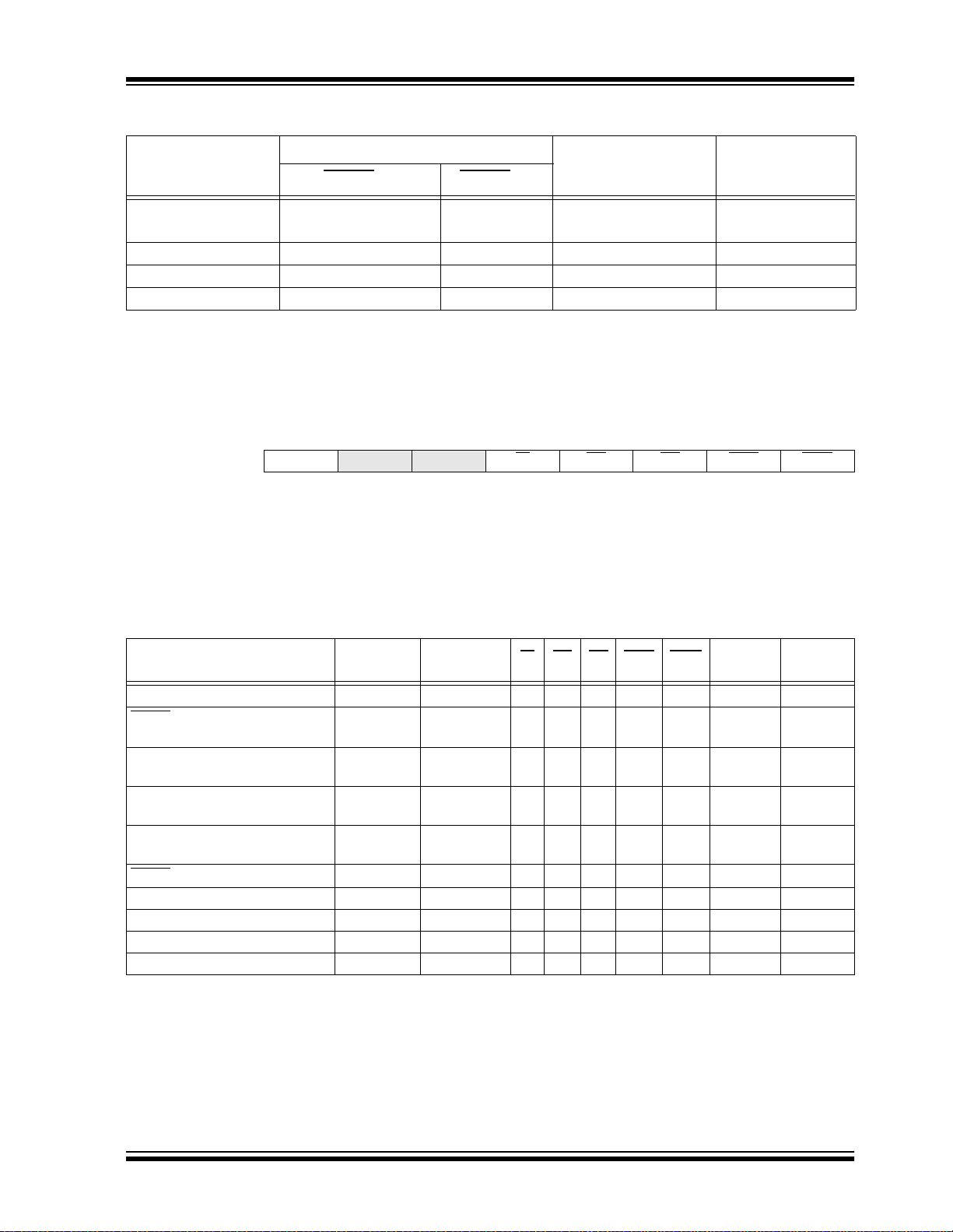
TABLE 3-1: TIME-OUT IN VARIOUS SITUATIONS
PIC18FXX2
Oscillator
Configuration
72 ms + 1024 TOSC
HS with PLL enabled
(1)
HS, XT, LP 72 ms + 1024 T
Power-up
PWRTE = 0 PWRTE = 1
+ 2ms
(2)
1024 TOSC
72 ms
+ 2 ms
OSC 1024 TOSC 72 ms
EC 72 ms — 72 ms
External RC 72 ms — 72 ms
Note 1: 2 ms is the nominal time required for the 4x PLL to lock.
2: 72 ms is the nominal power-up timer delay, if implemented.
REGISTER 3-1: RCON REGISTER BITS AND POSITIONS
R/W-0 U-0 U-0 R/W-1 R-1 R-1 R/W-0 R/W-0
IPEN — — RI TO PD POR BOR
bit 7 bit 0
Note 1: Refer to Section4.14 (page 53) for bit definitions.
Wake-up from
Brown-out
SLEEP or
Oscillator Switch
(2)
+ 1024 TOSC
+ 2 ms
(2)
+ 1024 TOSC 1024 TOSC
(2)
(2)
1024 T
OSC + 2 ms
—
—
TABLE 3-2: STATUS BITS, THEIR SIGNIFICANCE AND THE INITIALIZATION CONDITION FOR
RCON REGISTER
Condition
Program
Counter
Power-on Reset 0000h 0--1 1100 1 1 1 0 0 u u
MCLR Reset during normal
0000h 0--u uuuu u u u u u u u
operation
Software Reset during normal
0000h 0--0 uuuu 0 u u u u u u
operation
Stack Full Reset during normal
0000h 0--u uu11 u u u u u u 1
operation
Stack Underflow Reset during
0000h 0--u uu11 u u u u u 1 u
normal operation
MCLR
Reset during SLEEP 0000h 0--u 10uu u 1 0 u u u u
WDT Reset 0000h 0--u 01uu 1 0 1 u u u u
WDT Wake-up PC + 2 u--u 00uu u 0 0 u u u u
Brown-out Reset 0000h 0--1 11u0 1 1 1 1 0 u u
Interrupt wake-up from SLEEP PC + 2
(1)
Legend: u = unchanged, x = unknown, - = unimplemented bit, read as '0'
Note 1: When the wake-up is due to an interrupt and the GIEH or GIEL bits are set, the PC is loaded with the
interrupt vector (0x000008h or 0x000018h).
RCON
Register
TO PD POR BOR STKFUL STKUNF
RI
u--u 00uu u 1 0 u u u u
2002 Microchip Technology Inc. DS39564B-page 27

PIC18FXX2
TABLE 3-3: INITIALIZATION CONDITIONS FOR ALL REGISTERS
MCLR
Resets
Register Applicable Devices
Power-on Reset,
Brown-out Reset
TOSU 242 442 252 452 ---0 0000 ---0 0000 ---0 uuuu
TOSH 242 442 252 452 0000 0000 0000 0000 uuuu uuuu
TOSL 242 442 252 452 0000 0000 0000 0000 uuuu uuuu
STKPTR 242 442 252 452 00-0 0000 uu-0 0000 uu-u uuuu
PCLATU 242 442 252 452 ---0 0000 ---0 0000 ---u uuuu
PCLATH 242 442 252 452 0000 0000 0000 0000 uuuu uuuu
PCL 242 442 252 452 0000 0000 0000 0000 PC + 2
TBLPTRU 242 442 252 452 --00 0000 --00 0000 --uu uuuu
TBLPTRH 242 442 252 452 0000 0000 0000 0000 uuuu uuuu
TBLPTRL 242 442 252 452 0000 0000 0000 0000 uuuu uuuu
TABLAT 242 442 252 452 0000 0000 0000 0000 uuuu uuuu
PRODH 242 442 252 452 xxxx xxxx uuuu uuuu uuuu uuuu
PRODL 242 442 252 452 xxxx xxxx uuuu uuuu uuuu uuuu
INTCON 242 442 252 452 0000 000x 0000 000u uuuu uuuu
INTCON2 242 442 252 452 1111 -1-1 1111 -1-1 uuuu -u-u
INTCON3 242 442 252 452 11-0 0-00 11-0 0-00 uu-u u-uu
INDF0 242 442 252 452 N/A N/A N/A
POSTINC0 242 442 252 452 N/A N/A N/A
POSTDEC0 242 442 252 452 N/A N/A N/A
PREINC0 242 442 252 452 N/A N/A N/A
PLUSW0 242 442 252 452 N/A N/A N/A
FSR0H 242 442 252 452 ---- xxxx ---- uuuu ---- uuuu
FSR0L 242 442 252 452 xxxx xxxx uuuu uuuu uuuu uuuu
WREG 242 442 252 452 xxxx xxxx uuuu uuuu uuuu uuuu
INDF1 242 442 252 452 N/A N/A N/A
POSTINC1 242 442 252 452 N/A N/A N/A
POSTDEC1 242 442 252 452 N/A N/A N/A
PREINC1 242 442 252 452 N/A N/A N/A
PLUSW1 242 442 252 452 N/A N/A N/A
Legend: u = unchanged, x = unknown, - = unimplemented bit, read as ’0’, q = value depends on condition.
Shaded cells indicate condi tions do not apply for the designated devic e.
Note 1: One or more bits in the INTCONx or PIRx registers will be affected (to cause wake-up).
2: When the wak e-up is d ue to an interru pt and the G IEL or G IEH bit i s set, the PC is load ed with the int errup t
vector (0008h or 0018h).
3: When the wake-up is due to an interrupt and the GIEL or GIEH bit is set, the TOSU, TOSH and TOSL are
updated with the current value of the PC. The STKPTR is modified to point to the next location in the
hardware stack.
4: See Table 3-2 for RESET value for specific condition.
5: Bit 6 of PORTA, LATA, and TRISA are enabled in ECIO and RCIO Oscillator modes only. In all other
Oscillator modes, they are disabled and read ’0’.
6: Bit 6 of POR TA, LATA and TRISA are not available on all devices. Wh en unim plemente d, they are read ’0’.
WDT Reset
RESET Instruction
Stack Rese ts
Wake-up via WDT
or Interrupt
(3)
(3)
(3)
(3)
(2)
(1)
(1)
(1)
DS39564B-page 28 2002 Microchip Technology Inc.
 Loading...