


PIC18(L)F1XK22
Data Sheet
20-Pin Flash Microcontrollers
with nanoWatt XLP Technology
2009-2011 Microchip Technology Inc. DS41365E

Note the following details of the code protection feature on Microchip devices:
• Microchip products meet the specification contained in their particular Microchip Data Sheet.
• Microchip believes that its family of products is one of the most secure families of its kind on the market today, when used in the
intended manner and under normal conditions.
• There are dishonest and possibly illegal methods used to breach the code protection feature. All of these methods, to our
knowledge, require using the Microchip products in a manner outside the operating specifications contained in Microchip’s Data
Sheets. Most likely, the person doing so is engaged in theft of intellectual property.
• Microchip is willing to work with the customer who is concerned about the integrity of their code.
• Neither Microchip nor any other semiconductor manufacturer can guarantee the security of their code. Code protection does not
mean that we are guaranteeing the product as “unbreakable.”
Code protection is constantly evolving. We at Microchip are committed to continuously improving the code protection features of our
products. Attempts to break Microchip’s code protection feature may be a violation of the Digital Millennium Copyright Act. If such acts
allow unauthorized access to your software or other copyrighted work, you may have a right to sue for relief under that Act.
Information contained in this publication regarding device
applications and the like is provided only for your convenience
and may be superseded by updates. It is your responsibility to
ensure that your application meets with your specifications.
MICROCHIP MAKES NO REPRESENTATIONS OR
WARRANTIES OF ANY KIND WHETHER EXPRESS OR
IMPLIED, WRITTEN OR ORAL, STATUTORY OR
OTHERWISE, RELATED TO THE INFORMATION,
INCLUDING BUT NOT LIMITED TO ITS CONDITION,
QUALITY, PERFORMANCE, MERCHANTABILITY OR
FITNESS FOR PURPOSE. Microchip disclaims all liability
arising from this information and its use. Use of Microchip
devices in life support and/or safety applications is entirely at
the buyer’s risk, and the buyer agrees to defend, indemnify and
hold harmless Microchip from any and all damages, claims,
suits, or expenses resulting from such use. No licenses are
conveyed, implicitly or otherwise, under any Microchip
intellectual property rights.
Trademarks
The Microchip name and logo, the Microchip logo, dsPIC,
K
EELOQ, KEELOQ logo, MPLAB, PIC, PICmicro, PICSTART,
32
PIC
logo, rfPIC and UNI/O are registered trademarks of
Microchip Technology Incorporated in the U.S.A. and other
countries.
FilterLab, Hampshire, HI-TECH C, Linear Active Thermistor,
MXDEV, MXLAB, SEEVAL and The Embedded Control
Solutions Company are registered trademarks of Microchip
Technology Incorporated in the U.S.A.
Analog-for-the-Digital Age, Application Maestro, chipKIT,
chipKIT logo, CodeGuard, dsPICDEM, dsPICDEM.net,
dsPICworks, dsSPEAK, ECAN, ECONOMONITOR,
FanSense, HI-TIDE, In-Circuit Serial Programming, ICSP,
Mindi, MiWi, MPASM, MPLAB Certified logo, MPLIB,
MPLINK, mTouch, Omniscient Code Generation, PICC,
PICC-18, PICDEM, PICDEM.net, PICkit, PICtail, REAL ICE,
rfLAB, Select Mode, Total Endurance, TSHARC,
UniWinDriver, WiperLock and ZENA are trademarks of
Microchip Technology Incorporated in the U.S.A. and other
countries.
SQTP is a service mark of Microchip Technology Incorporated
in the U.S.A.
All other trademarks mentioned herein are property of their
respective companies.
© 2009-2011, Microchip Technology Incorporated, Printed in
the U.S.A., All Rights Reserved.
Printed on recycled paper.
ISBN: 978-1-61341-715-7
Microchip received ISO/TS-16949:2009 certification for its worldwide
headquarters, design and wafer fabrication facilities in Chandler and
Tempe, Arizona; Gresham, Oregon and design centers in California
and India. The Company’s quality system processes and procedures
are for its PIC
devices, Serial EEPROMs, microperipherals, nonvolatile memory and
analog products. In addition, Microchip’s quality system for the design
and manufacture of development systems is ISO 9001:2000 certified.
®
MCUs and dsPIC® DSCs, KEELOQ
®
code hopping
DS41365E-page 2 2009-2011 Microchip Technology Inc.

PIC18(L)F1XK22
20-Pin Flash Microcontrollers with nanoWatt XLP Technology
High-Performance RISC CPU:
• C Compiler Optimized Architecture:
- Optional extended instruction set designed to
optimize re-entrant code
• 256 bytes Data EEPROM
• Up to 16 Kbytes Linear Program Memory
Addressing
• Up to 512 bytes Linear Data Memory Addressing
• Up to 16 MIPS Operation
• 16-bit Wide Instructions, 8-bit Wide Data Path
• Priority Levels for Interrupts
• 31-Level, Software Accessible Hardware Stack
• 8 x 8 Single-Cycle Hardware Multiplier
Flexible Oscillator Structure:
• Precision 16 MHz Internal Oscillator Block:
- Factory calibrated to ± 1%
- Software selectable frequencies range of
31 kHz to 16 MHz
- 64 MHz performance available using PLL –
no external components required
• Four Crystal modes up to 64 MHz
• Two External Clock modes up to 64 MHz
• 4X Phase Lock Loop (PLL)
• Secondary Oscillator using Timer1 @ 32 kHz
• Fail-Safe Clock Monitor
- Allows for safe shutdown if peripheral clock
stops
• Two-Speed Oscillator Start-up
Special Microcontroller Features:
• 2.3V - 5.5V Operation – PIC18F1XK22
• 1.8V-3.6V Operation – PIC18LF1XK22
• Self-reprogrammable under Software Control
• Power-on Reset (POR), Power-up Timer (PWRT)
and Oscillator Start-up Timer (OST)
• Programmable Brown-out Reset (BOR)
• Extended Watchdog Timer (WDT):
- Programmable period from 4ms to 131s
• Programmable Code Protection
• In-Circuit Serial Programming™ (ICSP™) via
two pins
• In-Circuit Debug via Two Pins
Extreme Low-Power Management PIC18LF1XK22 with nanoWatt XLP:
• Sleep mode: 34 nA
• Watchdog Timer: 460 nA
• Timer1 Oscillator: 650 nA @ 32 kHz
Analog Features:
• Analog-to-Digital Converter (ADC) module
- 10-bit resolution, 12 channels
- Auto acquisition capability
- Conversion available during Sleep
• Analog Comparator module:
- Two rail-to-rail analog comparators
- Independent input multiplexing
- Inputs and outputs externally accessible
• Voltage Reference module:
- Programmable (% of V
- Two 16-level voltage ranges using V
- Programmable Fixed Voltage Reference
(FVR), 3 levels
DD), 16 steps
REF pins
Peripheral Highlights:
• 17 I/O Pins and 1 Input-only Pin:
- High current sink/source 25 mA/25 mA
- Programmable weak pull-ups
- Programmable interrupt-on- change
- Three external interrupt pins
• Four Timer modules:
- 3 16-bit timers/counters with prescaler
- 1 8-bit timer/counter with 8-bit period register,
prescaler and postscaler
- Dedicated, low-power Timer1 oscillator
• Enhanced Capture/Compare/PWM (ECCP)
module:
- One, two or four PWM outputs
- Selectable polarity
- Programmable dead time
- Auto-shutdown and Auto-restart
- PWM output steering control
• Master Synchronous Serial Port (MSSP) module
- 3-wire SPI (supports all 4 SPI modes)
2
C™ Master and Slave modes (Slave mode
-I
address masking)
• Enhanced Universal Synchronous Asynchronous
Receiver Transmitter module (EUSART)
- Supports RS-232, RS-485 and LIN 2.0
- Auto-Baud Detect
- Auto Wake-up on Break
• SR Latch (555 Timer) module with:
- Configurable inputs and outputs
- Supports mTouch™ capacitive sensing
applications
2009-2011 Microchip Technology Inc. DS41365E-page 3

PIC18(L)F1XK22
20-pin PDIP, SSOP, SOIC (300 MIL)
10
2
3
4
5
6
1
8
7
9
11
12
13
14
15
16
19
20
18
17
VDD
RA5
RA4
RA3/MCLR
/VPP
RC5
RC4
RC3/PGM
RC6
RC7
RB7
V
SS
RA0/PGD
RA1/PGC
RA2
RC0
RC1
RC2
RB4
RB5
RB6
PIC18(L)F13K22
PIC18(L)F14K22
-
89
2
3
1
14
15
16
10
11
6
12
13
17181920
7
5
4
PIC18(L)F13K22
PIC18(L)F14K22
RA3/MCLR/VPP
RC5
RC4
RC3/PGM
RC6
RC7
RB7
RB4
RB5
RB6
RC1
RC0
RA2
RA1/PGC
RA0/PGD
VSS
VDD
RA4
RA5
RC2
20-Pin QFN 4x4
TABLE 1: DEVICE OVERVIEW
Program Memory Data Memory
Device
PIC18F13K22
Bytes Words
8K 4K 256 256 20 18 12-ch 2 1 / 3 1 1 1 Yes
PIC18LF13K22
PIC18F14K22
16K 8K 512 256 20 18 12-ch 2 1 / 3 1 1 1 Yes
PIC18LF14K22
Note 1: One pin is input-only.
Pin Diagrams
SRAM
(bytes)
Data
EEPROM
(bytes)
Pins I/O
(1)
ECCP
Channels
10-bit A/D
Timers
Comparators
8-bit/16-bit
MSSP
EUSART
SR Latch
DS41365E-page 4 2009-2011 Microchip Technology Inc.

TABLE 2: PIC18(L)F1XK22 PIN SUMMARY
PIC18(L)F1XK22
I/O
20-Pin DIL
20-Pin QFN
19 16 RA0 AN0 C1IN+ VREF-/CVREF — — — — — IOC/INT0 Y
18 15 RA1 AN1 C12IN0- VREF+ — — — — — IOC/INT1 Y
17 14 RA2 AN2 C1OUT — — — — SRQ T0CKI IOC/INT2 Y —
4 1 RA3 — — — — — — — — IOC Y
3 20 RA4 AN3 — — — — — — — IOC Y
2 19 RA5 — — — — — — — T13CKI IOC Y
13 10 RB4 AN10 — — — — SDI/SDA — — IOC Y —
12 9 RB5 AN11 — — — RX/DT — — — IOC Y —
11 8 RB6 — — — — — SCL/SCK — — IOC Y —
10 7 RB7 — — — — TX/CK — — — IOC Y —
16 13 RC0 AN4 C2IN+ — — — — — — — — —
15 12 RC1 AN5 C12IN1- — — — — — — — —
14 11 RC2 AN6 C12IN2- — P1D — — — — — —
7 4 RC3 AN7 C12IN3- — P1C — — — — — — PGM
6 3 RC4 C2OUT — P1B — — SRNQ — — — —
5 2 RC5 — — — CCP1/P1A — — — — — — —
8 5 RC6 AN8 — — — — SS
9 6 RC7 AN9 — — — — SDO — — — — —
118—— — — — — — — — — — V
20 17 — — — — — — — — — — — VSS
Analog
Comparator
Reference
ECCP
EUSART
MSSP
—— —— —
Timers
SR Latch
Interrupts
Pull-up
Basic
PGD
PGC
MCLR/VPP
OSC2/CLKOUT
OSC1/CLKIN
DD
2009-2011 Microchip Technology Inc. DS41365E-page 5

PIC18(L)F1XK22
Table of Contents
1.0 Device Overview .......................................................................................................................................................................... 7
2.0 Oscillator Module........................................................................................................................................................................ 13
3.0 Memory Organization ................................................................................................................................................................. 25
4.0 Flash Program Memory.............................................................................................................................................................. 47
5.0 Data EEPROM Memory ............................................................................................................................................................. 57
6.0 8x8 Hardware Multiplier.............................................................................................................................................................. 61
7.0 Interrupts .................................................................................................................................................................................... 63
8.0 I/O Ports ..................................................................................................................................................................................... 77
9.0 Timer0 Module ........................................................................................................................................................................... 95
10.0 Timer1 Module ........................................................................................................................................................................... 99
11.0 Timer2 Module ......................................................................................................................................................................... 105
12.0 Timer3 Module ......................................................................................................................................................................... 107
13.0 Enhanced Capture/Compare/PWM (ECCP) Module ................................................................................................................ 111
14.0 Master Synchronous Serial Port (MSSP) Module .................................................................................................................... 133
15.0 Enhanced Universal Synchronous Asynchronous Receiver Transmitter (EUSART) ............................................................... 175
16.0 Analog-to-Digital Converter (ADC) Module .............................................................................................................................. 203
17.0 Comparator Module.................................................................................................................................................................. 217
18.0 Power-Managed Modes ........................................................................................................................................................... 229
19.0 SR Latch................................................................................................................................................................................... 235
20.0 Voltage References .................................................................................................................................................................. 239
21.0 Reset ........................................................................................................................................................................................ 245
22.0 Special Features of the CPU.................................................................................................................................................... 257
23.0 Instruction Set Summary .......................................................................................................................................................... 273
24.0 Development Support............................................................................................................................................................... 323
25.0 Electrical Specifications............................................................................................................................................................ 327
26.0 DC and AC Characteristics Graphs and Tables ....................................................................................................................... 363
27.0 Packaging Information.............................................................................................................................................................. 379
Appendix A: Revision History............................................................................................................................................................. 389
Appendix B: Device Differences......................................................................................................................................................... 389
TO OUR VALUED CUSTOMERS
It is our intention to provide our valued customers with the best documentation possible to ensure successful use of your Microchip
products. To this end, we will continue to improve our publications to better suit your needs. Our publications will be refined and
enhanced as new volumes and updates are introduced.
If you have any questions or comments regarding this publication, please contact the Marketing Communications Department via
E-mail at docerrors@microchip.com or fax the Reader Response Form in the back of this data sheet to (480) 792-4150. We
welcome your feedback.
Most Current Data Sheet
To obtain the most up-to-date version of this data sheet, please register at our Worldwide Web site at:
http://www.microchip.com
You can determine the version of a data sheet by examining its literature number found on the bottom outside corner of any page.
The last character of the literature number is the version number, (e.g., DS30000A is version A of document DS30000).
Errata
An errata sheet, describing minor operational differences from the data sheet and recommended workarounds, may exist for current
devices. As device/documentation issues become known to us, we will publish an errata sheet. The errata will specify the revision
of silicon and revision of document to which it applies.
To determine if an errata sheet exists for a particular device, please check with one of the following:
• Microchip’s Worldwide Web site; http://www.microchip.com
• Your local Microchip sales office (see last page)
When contacting a sales office, please specify which device, revision of silicon and data sheet (include literature number) you are
using.
Customer Notification System
Register on our web site at www.microchip.com to receive the most current information on all of our products.
DS41365E-page 6 2009-2011 Microchip Technology Inc.

PIC18(L)F1XK22
1.0 DEVICE OVERVIEW
This family offers the advantages of all PIC18
microcontrollers – namely, high computational
performance with the addition of high-endurance,
Flash program memory. On top of these features, the
PIC18(L)F1XK22 family introduces design
enhancements that make these microcontrollers a
logical choice for many high-performance, power
sensitive applications.
1.1 New Core Features
1.1.1 nanoWatt XLP TECHNOLOGY
All of the devices in the PIC18(L)F1XK22 family incorporate a range of features that can significantly reduce
power consumption during operation. Key items
include:
• Multiple Idle Modes: The controller can also run
with its CPU core disabled but the peripherals still
active. In these states, power consumption can be
reduced even further, to as little as 4% of normal
operation requirements.
• On-the-fly Mode Switching: The
power-managed modes are invoked by user code
during operation, allowing the user to incorporate
power-saving ideas into their application’s
software design.
• Low Consumption in Key Modules: The
power requirements for both Timer1 and the
Watchdog Timer are minimized. See
Section 25.0 “Electrical Specifications”
for values.
1.1.2 MULTIPLE OSCILLATOR OPTIONS AND FEATURES
All of the devices in the PIC18(L)F1XK22 family offer
ten different oscillator options, allowing users a wide
range of choices in developing application hardware.
These include:
• Four Crystal modes, using crystals or ceramic
resonators
• External Clock modes, offering the option of using
two pins (oscillator input and a divide-by-4 clock
output) or one pin (oscillator input, with the second pin reassigned as general I/O)
• External RC Oscillator modes with the same pin
options as the External Clock modes
• An internal oscillator block which contains a
16 MHz HFINTOSC oscillator and a 31 kHz
LFINTOSC oscillator which together provide 8
user selectable clock frequencies, from 31 kHz to
16 MHz. This option frees the two oscillator pins
for use as additional general purpose I/O.
• A Phase Lock Loop (PLL) frequency multiplier,
available to both the high-speed crystal and internal oscillator modes, which allows clock speeds of
up to 64 MHz. Used with the internal oscillator, the
PLL gives users a complete selection of clock
speeds, from 31 kHz to 32 MHz – all without using
an external crystal or clock circuit.
Besides its availability as a clock source, the internal
oscillator block provides a stable reference source that
gives the family additional features for robust
operation:
• Fail-Safe Clock Monitor: This option constantly
monitors the main clock source against a reference signal provided by the LFINTOSC. If a clock
failure occurs, the controller is switched to the
internal oscillator block, allowing for continued
operation or a safe application shutdown.
• Two-Speed Start-up: This option allows the
internal oscillator to serve as the clock source
from Power-on Reset, or wake-up from Sleep
mode, until the primary clock source is available.
2009-2011 Microchip Technology Inc. DS41365E-page 7

PIC18(L)F1XK22
1.2 Other Special Features
• Memory Endurance: The Flash cells for both
program memory and data EEPROM are rated to
last for many thousands of erase/write cycles – up to
10K for program memory and 100K for EEPROM.
Data retention without refresh is conservatively
estimated to be greater than 40 years.
• Self-programmability: These devices can write
to their own program memory spaces under
internal software control. Using a bootloader
routine located in the code protected Boot Block,
it is possible to create an application that can
update itself in the field.
• Extended Instruction Set: The PIC18(L)F1XK22
family introduces an optional extension to the
PIC18 instruction set, which adds 8 new instructions and an Indexed Addressing mode. This
extension has been specifically designed to optimize re-entrant application code originally developed in high-level languages, such as C.
• Enhanced CCP module: In PWM mode, this
module provides 1, 2 or 4 modulated outputs for
controlling half-bridge and full-bridge drivers.
Other features include:
- Auto-Shutdown, for disabling PWM outputs
on interrupt or other select conditions
- Auto-Restart, to reactivate outputs once the
condition has cleared
- Output steering to selectively enable one or
more of 4 outputs to provide the PWM signal.
• Enhanced Addressable USART: This serial
communication module is capable of standard
RS-232 operation and provides support for the LIN
bus protocol. Other enhancements include
automatic baud rate detection and a 16-bit Baud
Rate Generator for improved resolution.
• 10-bit A/D Converter: This module incorporates
programmable acquisition time, allowing for a
channel to be selected and a conversion to be
initiated without waiting for a sampling period and
thus, reduce code overhead.
• Extended Watchdog Timer (WDT): This
enhanced version incorporates a 16-bit
postscaler, allowing an extended time-out range
that is stable across operating voltage and
temperature. See Section 25.0 “Electrical
Specifications” for time-out periods.
1.3 Details on Individual Family Members
Devices in the PIC18(L)F1XK22 family are available in
20-pin packages. Block diagrams for the two groups
are shown in Figure 1-1.
The devices are differentiated from each other in the
following ways:
1. Flash program memory:
• 8 Kbytes for PIC18(L)F13K22
• 16 Kbytes for PIC18(L)F14K22
All other features for devices in this family are identical.
These are summarized in Ta bl e 1 - 1 .
The pinouts for all devices are listed in Tab l e 2 and I/O
description are in Table 1-2.
DS41365E-page 8 2009-2011 Microchip Technology Inc.

PIC18(L)F1XK22
TABLE 1-1: DEVICE FEATURES FOR THE PIC18(L)F1XK22 (20-PIN DEVICES)
Features PIC18F13K22 PIC18LF13K22 PIC18F14K22 PIC18LF14K22
Voltage Range (1.8 - 5.5V) 2.3-5.5V 1.8V-3.6V 2.3-5.5V 1.8V-3.6V
Program Memory (Bytes) 8K 16K
Program Memory (Instructions) 4096 8192
Data Memory (Bytes) 256 512
Operating Frequency DC – 64 MHz
Interrupt Sources 30
I/O Ports Ports A, B, C
Timers 4
Enhanced Capture/ Compare/PWM Modules 1
Serial Communications MSSP, Enhanced USART
10-Bit Analog-to-Digital Module 12 Input Channels
Resets (and Delays) POR, BOR, RESET Instruction, Stack Full, Stack Underflow, MCLR
(PWRT, OST)
Instruction Set 75 Instructions, 83 with Extended Instruction Set Enabled
Packages 20-Pin PDIP, SSOP, SOIC (300 mil)
QFN (4x4x0.9mm)
, WDT
2009-2011 Microchip Technology Inc. DS41365E-page 9

PIC18(L)F1XK22
Instruction
Decode and
Control
PORTA
PORTB
PORTC
RA1
RA0
Data Latch
Data Memory
Address Latch
Data Address<12>
12
Access
BSR
FSR0
FSR1
FSR2
inc/dec
logic
Address
4
12
4
PCH PCL
PCLATH
8
31-Level Stack
Program Counter
PRODLPRODH
8 x 8 Multiply
8
BITOP
8
8
ALU<8>
20
8
8
Table Pointer<21>
inc/dec logic
21
8
Data Bus<8>
Table Latch
8
IR
12
3
ROM Latch
PCLATU
PCU
Note 1: RA3 is only available when MCLR functionality is disabled.
2: OSC1/CLKIN and OSC2/CLKOUT are only available in select oscillator modes and when these pins are not being used
as digital I/O. Refer to Section 2.0 “Oscillator Module” for additional information.
EUSARTComparator
MSSP
10-bit
ADC
Timer2Timer1 Timer3Timer0
ECCP1
BOR
Data
EEPROM
W
Instruction Bus <16>
STKPTR
Bank
8
State machine
control signals
Decode
8
8
Power-up
Timer
Oscillator
Start-up Timer
Power-on
Reset
Watchdog
Timer
OSC1
(2)
OSC2
(2)
VDD,
Internal
Oscillator
Fail-Safe
Clock Monitor
Precision
Reference
Band Gap
V
SS
MCLR
(1)
Block
LFINTOSC
Oscillator
16 MHz
Oscillator
Single-Supply
Programming
FVR
FVR
FVR
CVREF
Address Latch
Program Memory
Data Latch
CVREF
RA3
RA4
RA5
RB4
RB5
RB6
RB7
RC0
RC1
RC2
RC3
RC4
RC5
RC6
RC7
(512/768 bytes)
RA1
FIGURE 1-1: PIC18(L)F1XK22 BLOCK DIAGRAM
DS41365E-page 10 2009-2011 Microchip Technology Inc.

PIC18(L)F1XK22
TABLE 1-2: PIC18(L)F1XK22 PIN SUMMARY
Pin
Pin Name
RA0/AN0/CVREF/VREF-/C1IN+/INT0/PGD
RA0
AN0
REF
CV
VREFC1IN+
INT0
PGD
RA1/AN1/C12IN0-/V
RA1
AN1
C12IN0V
REF+
INT1
PGC
RA2/AN2/C1OUT/T0CKI/INT2/SRQ
RA2
AN2
C1OUT
T0CKI
INT2
SRQ
RA3/MCLR
RA4/AN3/OSC2/CLKOUT
RA5/OSC1/CLKIN/T13CKI
RB4/AN10/SDI/SDA
RB5/AN11/RX/DT
Legend: TTL = TTL compatible input CMOS = CMOS compatible input or output
/VPP
RA3
MCLR
VPP
RA4
AN3
OSC2
CLKOUT
RA5
OSC1
CLKIN
T13CKI
RB4
AN10
SDI
SDA
RB5
AN11
RX
DT
ST = Schmitt Trigger input I = Input
O = Output P = Power
XTAL= Crystal Oscillator
REF+/INT1/PGC
Number
DIL
19 16
18 15
17 14
41
320
219
13 10
12 9
Pin
Buffer
Typ e
QFN
I/O
I/O
I/O
I/O
I/O
—
I/O
I/O
I/O
I/O
I/O
I/O
Typ e
TTL
I
Analog
O
Analog
I
Analog
I
Analog
I
ST
ST
TTL
I
Analog
1
Analog
I
Analog
I
ST
ST
ST
I
Analog
CMOS
I
ST
I
ST
O
CMOS
I
ST
I
ST
P
O
O
—
TTL
I
Analog
XTAL
CMOS
TTL
I
XTAL
I
CMOS
I
ST
TTL
I
Analog
I
ST
ST
TLL
I
Analog
I
ST
ST
Digital I/O
ADC channel 0
DAC reference voltage output
ADC and DAC reference voltage (low) input
Comparator C1 non-inverting input
External interrupt 0
ICSP™ programming data pin
Digital I/O
ADC channel 1
Comparator C1 and C2 non-inverting input
ADC and DAC reference voltage (high) input
External interrupt 1
ICSP™ programming clock pin
Digital I/O
ADC channel 2
Comparator C1 output
Timer0 external clock input
External interrupt 2
SR latch output
Digital input
Active-low Master Clear with internal pull-up
High voltage programming input
Digital I/O
ADC channel 3
Oscillator crystal output. Connect to crystal or resonator
in Crystal Oscillator mode
In RC mode, OSC2 pin outputs CLKOUT which
has 1/4 the frequency of OSC1 and denotes
the instruction cycle rate
Digital I/O
Oscillator crystal input or external clock input
ST buffer when configured in RC mode; analog other
wise
External clock source input. Always associated with the
pin function OSC1 (See related OSC1/CLKIN, OSC2,
CLKOUT pins
Timer0 and Timer3 external clock input
Digital I/O
ADC channel 10
SPI data in
2
C™ data I/O
I
Digital I/O
ADC channel 11
EUSART asynchronous receive
EUSART synchronous data (see related RX/TX)
Description
2009-2011 Microchip Technology Inc. DS41365E-page 11

PIC18(L)F1XK22
TABLE 1-2: PIC18(L)F1XK22 PIN SUMMARY
Pin
Pin Name
RB6/SCK/SCL
RB6
SCK
SCL
RB7/TX/CK
RB7
TX
CK
RC0/AN4/C2IN+
RC0
AN4
C2IN+
RC1/AN5/C12IN-/INT1
RC1
AN5
C12ININT1
RC2/AN6/C12IN2-/P1D/INT2
RC2
AN6
C12IN2P1D
RC3/AN7/C12IN3-/P1C/PGM
RC3
AN7
C12IN3P1C
PGM
RC4/C12OUT/P1B/SRQ
RC4
C12OUT
P1B
SRNQ
RC5/CCP1/P1A
RC5
CCP1
P1A
RC6/AN8/SS
RC6
AN8
SS
RC7/AN9/SDO
RC7
AN9
SDO
V
SS 20 17 P — Ground reference for logic and I/O pins
V
DD 1 18 P — Positive supply for logic and I/O pins
Legend: TTL = TTL compatible input CMOS = CMOS compatible input or output
ST = Schmitt Trigger input I = Input
O = Output P = Power
XTAL= Crystal Oscillator
Number
DIL
11 8
10 7
16 13
15 12
14 11
74
63
52
85
96
Pin
Buffer
Typ e
Typ e
QFN
I/O
I/O
I/O
I/O
O
I/O
I/O
I/O
I/O
O
I/O
O
I/O
I/O
O
O
O
I/O
I/O
O
I/O
I/O
O
TLL
ST
ST
TLL
CMOS
ST
ST
I
Analog
I
Analog
ST
I
Analog
I
Analog
I
ST
ST
I
Analog
I
Analog
CMOS
ST
I
Analog
I
Analog
CMOS
ST
ST
CMOS
CMOS
CMOS
ST
ST
CMOS
ST
I
Analog
I
TTL
ST
I
Analog
CMOS
Digital I/O
Synchronous serial clock input/output for SPI mode
Synchronous serial clock input/output for I
Digital I/O
EUSART asynchronous transmit
EUSART synchronous clock (see related RX/DT)
Digital I/O
ADC channel 4
Comparator C2 non-inverting input
Digital I/O
ADC channel 5
Comparator C1 and C2 non-inverting input
External interrupt 0
Digital I/O
ADC channel 6
Comparator C1 and C2 inverting input
Enhanced CCP1 PWM output
Digital I/O
ADC channel 7
Comparator C1 and C2 inverting input
Enhanced CCP1 PWM output
Low-Voltage ICSP Programming enable pin
Digital I/O
Comparator C1 and C2 output
Enhanced CCP1 PWM output
SR latch output
Digital I/O
Capture 1 input/Compare 1 output/PWM 1 output
Enhanced CCP1 PWM output
Digital I/O
ADC channel 8
SPI slave select input
Digital I/O
ADC channel 9
SPI data out
Description
2
C™ mode
DS41365E-page 12 2009-2011 Microchip Technology Inc.

PIC18(L)F1XK22
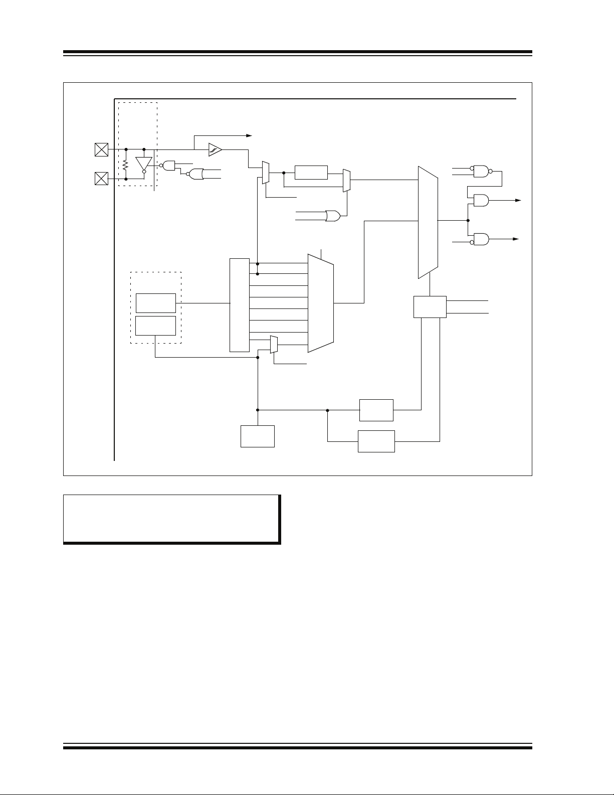
2.0 OSCILLATOR MODULE
2.1 Overview
The oscillator module has a variety of clock sources
and features that allow it to be used in a wide range of
applications, maximizing performance and minimizing
power consumption. Figure 2-1 illustrates a block
diagram of the oscillator module.
Key features of the oscillator module include:
•System Clocks
• System Clock Selection
- Primary External Oscillator
- Secondary External Oscillator
- Internal Oscillator
• Oscillator Start-up Timer
• System Clock Selection
• Clock Switching
• 4x Phase Lock Loop Frequency Multiplier
• CPU Clock Divider
• Two-Speed Start-up Mode
• Fail-Safe Clock Monitoring
2.2 System Clocks
The PIC18(L)F1XK22 can be operated in 13 different
oscillator modes. The user can program these using
the available Configuration bits. In addition, clock support functions such as Fail-Safe and two Start-up can
also be configured.
The available Primary oscillator options include:
• External Clock, low power (ECL)
• External Clock, medium power (ECM)
• External Clock, high power (ECH)
• External Clock, low power, CLKOUT function on
RA4/OSC2 (ECCLKOUTL)
• External Clock, medium power, CLKOUT function
on RA4/OSC2 (ECCLKOUTM)
• External Clock, high power, CLKOUT function on
RA4/OSC2 (ECCLKOUTH)
•External Crystal (XT)
• High-speed Crystal (HS)
• Low-power crystal (LP)
• External Resistor/Capacitor (EXTRC)
• External RC, CLKOUT function on RA4/OSC2
• 31.25 kHz – 16 MHz internal oscillator (INTOSC)
• 31.25 kHz – 16 MHz internal oscillator, CLKOUT
function on RA4/OSC2
Additionally, the 4xPLL may be enabled in hardware or
software (under certain conditions) for increased oscillator speed.
2.3 System Clock Selection
The SCS bits of the OSCCON register select between
the following clock sources:
• Primary External Oscillator
• Secondary External Oscillator
• Internal Oscillator
Note: The frequency of the system clock will be
referred to as F
document.
OSC throughout this
TABLE 2-1: SYSTEM CLOCK SELECTION
Configuration Selection
SCS <1:0> System Clock
1x Internal Oscillator
01 Secondary External Oscillator
00
(Default after Reset)
The default state of the SCS bits sets the system clock
to be the oscillator defined by the FOSC bits of the
CONFIG1H Configuration register. The system clock
will always be defined by the FOSC bits until the SCS
bits are modified in software.
When the Internal Oscillator is selected as the system
clock, the IRCF bits of the OSCCON register and the
INTSRC bit of the OSCTUNE register will select either
the LFINTOSC or the HFINTOSC. The LFINTOSC is
selected when the IRCF<2:0> = 000 and the INTSRC
bit is clear. All other combinations of the IRCF bits and
the INTSRC bit will select the HFINTOSC as the
system clock.
Oscillator defined by
FOSC<3:0>
2.4 Primary External Oscillator
The Primary External Oscillator’s mode of operation is
selected by setting the FOSC<3:0> bits of the
CONFIG1H Configuration register. The oscillator can
be set to the following modes:
• LP: Low-Power Crystal
• XT: Crystal/Ceramic Resonator
• HS: High-Speed Crystal Resonator
• RC: External RC Oscillator
• EC: External Clock
Additionally, the Primary External Oscillator may be
shut-down under firmware control to save power.
2009-2011 Microchip Technology Inc. DS41365E-page 13
PIC18(L)F1XK22
4 x PLL
FOSC<3:0>
OSC2
OSC1/T13CKI
Sleep
CPU
Peripherals
IDLEN
Postscaler
MUX
MUX
16 MHz
8 MHz
4 MHz
2 MHz
1 MHz
250 kHz
500 kHz
IRCF<2:0>
0x
110
101
100
011
010
001
000
31 kHz
31 kHz
LFINTOSC
Internal
Oscillator
Block
Clock
Control
SCS<1:0>
HFINTOSC
16 MHz
0
1
INTSRC
Primary
PIC18(L)F1XK22
Sleep
Sleep
System
PCLKEN
PRI_SD
0
1
FOSC<3:0>
PLL_EN
PLLEN
Oscillator,
Watchdog
Time r
Fail-Safe
Clock
Two-Speed
Star t-up
Clock
Timer1/Timer3
External
Secondary
Oscillator
and
LP, XT, HS, RC, EC,
Secondary Osc.
T1OSCEN
Internal Osc.
1x
FIGURE 2-1: PIC® MCU CLOCK SOURCE BLOCK DIAGRAM
Note: If using a low-frequency external oscillator
and want to multiple it by 4 via PLL, the
ideal input frequency is from 4 MHz to 16
MHz.
DS41365E-page 14 2009-2011 Microchip Technology Inc.

PIC18(L)F1XK22
Note 1: A series resistor (RS) may be required for
quartz crystals with low drive level.
2: The value of R
F varies with the Oscillator mode
selected (typically between 2 M to 10 M.
C1
C2
Quartz
R
S
(1)
OSC1/CLKIN
RF
(2)
Sleep
To Internal
Logic
PIC® MCU
Crystal
OSC2/CLKOUT
2.4.1 PRIMARY EXTERNAL OSCILLATOR
SHUT-DOWN
The Primary External Oscillator can be enabled or disabled via software. To enable software control of the
Primary External Oscillator, the PCLKEN bit of the
CONFIG1H Configuration register must be set. With
the PCLKEN bit set, the Primary External Oscillator is
controlled by the PRI_SD bit of the OSCCON2 register.
The Primary External Oscillator will be enabled when
the PRI_SD bit is set, and disabled when the PRI_SD
bit is clear.
Note: The Primary External Oscillator cannot be
shut down when it is selected as the
System Clock. To shut down the oscillator,
the system clock source must be either
the Secondary Oscillator or the Internal
Oscillator.
2.4.2 LP, XT AND HS OSCILLATOR
MODES
The LP, XT and HS modes support the use of quartz
crystal resonators or ceramic resonators connected to
OSC1 and OSC2 (Figure 2-2). The mode selects a low,
medium or high gain setting of the internal inverteramplifier to support various resonator types and speed.
LP Oscillator mode selects the lowest gain setting of the
internal inverter-amplifier. LP mode current consumption
is the least of the three modes. This mode is best suited
to drive resonators with a low drive level specification, for
example, tuning fork type crystals.
XT Oscillator mode selects the intermediate gain
setting of the internal inverter-amplifier. XT mode
current consumption is the medium of the three modes.
This mode is best suited to drive resonators with a
medium drive level specification.
HS Oscillator mode selects the highest gain setting of the
internal inverter-amplifier. HS mode current consumption
is the highest of the three modes. This mode is best
suited for resonators that require a high drive setting.
Figure 2-2 and Figure 2-3 show typical circuits for
quartz crystal and ceramic resonators, respectively.
FIGURE 2-2: QUARTZ CRYSTAL
OPERATION (LP, XT OR
HS MODE)
Note 1: Quartz crystal characteristics vary
according to type, package and
manufacturer. The user should consult the
manufacturer data sheets for specifications
and recommended application.
2: Always verify oscillator performance over
DD and temperature range that is
the V
expected for the application.
3: For oscillator design assistance, reference
the following Microchip Applications Notes:
• AN826, “Crystal Oscillator Basics and
Crystal Selection for rfPIC
Devices” (DS00826)
• AN849, “Basic PIC
(DS00849)
• AN943, “Practical PIC
Analysis and Design” (DS00943)
• AN949, “Making Your Oscillator Work”
(DS00949)
®
and PIC®
®
Oscillator Design”
®
Oscillator
2009-2011 Microchip Technology Inc. DS41365E-page 15

PIC18(L)F1XK22
Note 1: A series resistor (RS) may be required for
ceramic resonators with low drive level.
2: The value of R
F varies with the Oscillator mode
selected (typically between 2 M to 10 M.
3: An additional parallel feedback resistor (R
P)
may be required for proper ceramic resonator
operation.
C1
C2
Ceramic
R
S
(1)
OSC1/CLKIN
RF
(2)
Sleep
To Internal
Logic
PIC® MCU
RP
(3)
Resonator
OSC2/CLKOUT
OSC2/CLKOUT
(1)
CEXT
REXT
PIC® MCU
OSC1/CLKIN
F
OSC/4 or
Internal
Clock
VDD
VSS
Recommended values: 10 k REXT 100 k
C
EXT > 20 pF
Note 1: Alternate pin functions are listed in
Section 1.0 “Device Overview”.
2: Output depends upon RC or RCIO clock mode.
I/O
(2)
FIGURE 2-3: CERAMIC RESONATOR
OPERATION
(XT OR HS MODE)
2.4.3 EXTERNAL RC
The External Resistor-Capacitor (RC) mode supports
the use of an external RC circuit. This allows the
designer maximum flexibility in frequency choice while
keeping costs to a minimum when clock accuracy is not
required. In RC mode, the RC circuit connects to OSC1,
allowing OSC2 to be configured as an I/O or as
CLKOUT. The CLKOUT function is selected by the
FOSC bits of the CONFIG1H Configuration register.
When OSC2 is configured as CLKOUT, the frequency
at the pin is the frequency of the RC oscillator divided by
4. Figure 2-4 shows the external RC mode connections.
FIGURE 2-4: EXTERNAL RC MODES
The RC oscillator frequency is a function of the supply
voltage, the resistor R
EXT, the capacitor CEXT and the
operating temperature. Other factors affecting the
oscillator frequency are:
• Input threshold voltage variation
• Component tolerances
• Variation in capacitance due to packaging
2.4.4 EXTERNAL CLOCK
The External Clock (EC) mode allows an externally
generated logic level clock to be used as the system’s
clock source. When operating in this mode, the
external clock source is connected to the OSC1
allowing OSC2 to be configured as an I/O or as
CLKOUT. The CLKOUT function is selected by the
FOSC bits of the CONFIG1H Configuration register.
When OSC2 is configured as CLKOUT, the frequency
at the pin is the frequency of the EC oscillator divided
by 4.
Three different power settings are available for EC
mode. The power settings allow for a reduced I
DD of the
device, if the EC clock is known to be in a specific
range. If there is an expected range of frequencies for
the EC clock, select the power mode for the highest
frequency.
EC Low power 0 – 250 kHz
EC Medium power 250 kHz – 4 MHz
EC High power 4 – 64 MHz
2.5 Secondary External Oscillator
The Secondary External Oscillator is designed to drive
an external 32.768 kHz crystal. This oscillator is
enabled or disabled by the T1OSCEN bit of the T1CON
register. See Section 10.0 “Timer1 Module” for more
information.
DS41365E-page 16 2009-2011 Microchip Technology Inc.

PIC18(L)F1XK22
2.6 Internal Oscillator
The internal oscillator module contains two independent
oscillators which are:
• LFINTOSC: Low-Frequency Internal Oscillator
• HFINTOSC: High-Frequency Internal Oscillator
When operating with either oscillator, OSC1 will be an
I/O and OSC2 will be either an I/O or CLKOUT. The
CLKOUT function is selected by the FOSC bits of the
CONFIG1H Configuration register. When OSC2 is
configured as CLKOUT, the frequency at the pin is the
frequency of the Internal Oscillator divided by 4.
2.6.1 LFINTOSC
The Low-Frequency Internal Oscillator (LFINTOSC) is
a 31 kHz internal clock source. The LFINTOSC
oscillator is the clock source for:
• Power-up Timer
• Watchdog Timer
• Fail-Safe Clock Monitor
The LFINTOSC is enabled when any of the following
conditions are true:
• Power-up Timer is enabled (PWRTEN = 0)
• Watchdog Timer is enabled (WDTEN = 1)
• Watchdog Timer is enabled by software
(WDTEN = 0 and SWDTEN = 1)
• Fail-Safe Clock Monitor is enabled (FCMEM = 1)
•SCS1=1 and IRCF<2:0> = 000 and INTSRC = 0
• FOSC<3:0> selects the internal oscillator as the
primary clock and IRCF<2:0> = 000 and
INTSRC = 0
• IESO = 1 (Two-Speed Start-up) and
IRCF<2:0> = 000 and INTSRC = 0
2.6.2 HFINTOSC
The High-Frequency Internal Oscillator (HFINTOSC) is
a precision oscillator that is factory-calibrated to
operate at 16 MHz. The output of the HFINTOSC
connects to a postscaler and a multiplexer (see
Figure 2-1). One of eight frequencies can be selected
using the IRCF<2:0> bits of the OSCCON register. The
following frequencies are available from the
HFINTOSC:
•16 MHZ
•8 MHZ
•4 MHZ
•2 MHZ
• 1 MHZ (Default after Reset)
•500 kHz
•250 kHz
•31 kHz
The HFIOFS bit of the OSCCON register indicates
whether the HFINTOSC is stable.
Note 1: Selecting 31 kHz from the HFINTOSC
oscillator requires IRCF<2:0> = 000 and
the INTSRC bit of the OSCTUNE register
to be set. If the INTSRC bit is clear, the
system clock will come from the
LFINTOSC.
2: Additional adjustments to the frequency
of the HFINTOSC can made via the
OSCTUNE registers. See Register 2-3
for more details.
The HFINTOSC is enabled if any of the following
conditions are true:
•SCS1=1 and IRCF<2:0> 000
•SCS1=1 and IRCF<2:0> = 000 and INTSRC = 1
• FOSC<3:0> selects the internal oscillator as the
primary clock and
- IRCF<2:0> 000 or
- IRCF<2:0> = 000 and INTSRC = 1
• IESO = 1 (Two-Speed Start-up) and
- IRCF<2:0> 000 or
- IRCF<2:0> = 000 and INTSRC = 1
•FCMEM=1 (Fail-Safe Clock Monitoring) and
- IRCF<2:0> 000 or
- IRCF<2:0> = 000 and INTSRC = 1
2009-2011 Microchip Technology Inc. DS41365E-page 17

PIC18(L)F1XK22
2.7 Oscillator Control
The Oscillator Control (OSCCON) (Register 2-1) and the
Oscillator Control 2 (OSCCON2) (Register 2-2) registers
control the system clock and frequency selection
options.
REGISTER 2-1: OSCCON: OSCILLATOR CONTROL REGISTER
R/W-0 R/W-0 R/W-1 R/W-1 R-q R-0 R/W-0 R/W-0
IDLEN IRCF2 IRCF1 IRCF0 OSTS
bit 7 bit 0
Legend:
R = Readable bit W = Writable bit U = Unimplemented bit, read as ‘0’ q = depends on condition
-n = Value at POR ‘1’ = Bit is set ‘0’ = Bit is cleared x = Bit is unknown
bit 7 IDLEN: Idle Enable bit
1 = Device enters Idle mode on SLEEP instruction
0 = Device enters Sleep mode on SLEEP instruction
bit 6-4 IRCF<2:0>: Internal Oscillator Frequency Select bits
111 = 16 MHz
110 = 8 MHz
101 = 4 MHz
100 = 2 MHz
011 = 1 MHz
010 = 500 kHz
001 = 250 kHz
000 = 31 kHz
bit 3 OSTS: Oscillator Start-up Time-out Status bit
1 = Device is running from the clock defined by FOSC<2:0> of the CONFIG1 register
0 = Device is running from the internal oscillator (HFINTOSC or LFINTOSC)
bit 2 HFIOFS: HFINTOSC Frequency Stable bit
1 = HFINTOSC frequency is stable
0 = HFINTOSC frequency is not stable
bit 1-0 SCS<1:0>: System Clock Select bits
1x = Internal oscillator block
01 = Secondary (Timer1) oscillator
00 = Primary clock (determined by CONFIG1H[FOSC<3:0>]).
(3)
(2)
(1)
(1)
HFIOFS SCS1 SCS0
Note 1: Reset state depends on state of the IESO Configuration bit.
2: Source selected by the INTSRC bit of the OSCTUNE register, see text.
3: Default output frequency of HFINTOSC on Reset.
DS41365E-page 18 2009-2011 Microchip Technology Inc.

PIC18(L)F1XK22
REGISTER 2-2: OSCCON2: OSCILLATOR CONTROL REGISTER 2
U-0 U-0 U-0 U-0 U-0 R/W-1 R/W-0 R-x
— — — — — PRI_SD HFIOFL LFIOFS
bit 7 bit 0
Legend:
R = Readable bit W = Writable bit U = Unimplemented bit, read as ‘0’ q = depends on condition
-n = Value at POR ‘1’ = Bit is set ‘0’ = Bit is cleared x = Bit is unknown
bit 7-3 Unimplemented: Read as ‘0’
bit 2 PRI_SD: Primary Oscillator Drive Circuit shutdown bit
1 = Oscillator drive circuit on
0 = Oscillator drive circuit off (zero power)
bit 1 HFIOFL: HFINTOSC Frequency Locked bit
1 = HFINTOSC is in lock
0 = HFINTOSC has not yet locked
bit 0 LFIOFS: LFINTOSC Frequency Stable bit
1 = LFINTOSC is stable
0 = LFINTOSC is not stable
2009-2011 Microchip Technology Inc. DS41365E-page 19

PIC18(L)F1XK22
2.7.1 OSCTUNE REGISTER
The HFINTOSC is factory calibrated, but can be
adjusted in software by writing to the TUN<5:0> bits of
the OSCTUNE register (Register 2-3).
The default value of the TUN<5:0> is ‘000000’. The
value is a 6-bit two’s complement number.
When the OSCTUNE register is modified, the
HFINTOSC frequency will begin shifting to the new
frequency. Code execution continues during this shift,
while giving no indication that the shift has occurred.
OSCTUNE does not affect the LFINTOSC frequency.
The operation of features that depend on the LFINTOSC
clock source frequency, such as the Power-up Timer
(PWRT), Watchdog Timer (WDT), Fail-Safe Clock Monitor (FSCM) and peripherals, are not affected by the
change in frequency.
The OSCTUNE register also implements the INTSRC
and PLLEN bits, which control certain features of the
internal oscillator block.
The INTSRC bit allows users to select which internal
oscillator provides the clock source when the 31 kHz
frequency option is selected. This is covered in greater
detail in Section 2.6.1 “LFINTOSC”.
The PLLEN bit controls the operation of the frequency
multiplier. For more details about the function of the
PLLEN bit see Section 2.10 “4x Phase Lock Loop
Frequency Multiplier”
REGISTER 2-3: OSCTUNE: OSCILLATOR TUNING REGISTER
R/W-0 R/W-0 R/W-0 R/W-0 R/W-0 R/W-0 R/W-0 R/W-0
INTSRC PLLEN TUN5 TUN4 TUN3 TUN2 TUN1 TUN0
bit 7 bit 0
Legend:
R = Readable bit W = Writable bit U = Unimplemented bit, read as ‘0’
-n = Value at POR ‘1’ = Bit is set ‘0’ = Bit is cleared x = Bit is unknown
bit 7 INTSRC: Internal Oscillator Low-Frequency Source Select bit
1 = 31.25 kHz device clock derived from 16 MHz HFINTOSC source (divide-by-512 enabled)
0 = 31 kHz device clock derived directly from LFINTOSC internal oscillator
bit 6 PLLEN: Frequency Multiplier PLL bit
1 = PLL enabled (for HFINTOSC 8 MHz and 16 MHz only)
0 = PLL disabled
bit 5-0 TUN<5:0>: Frequency Tuning bits
011111 = Maximum frequency
011110 =
• • •
000001 =
000000 = Oscillator module is running at the factory calibrated frequency.
111111 =
• • •
100000 = Minimum frequency
DS41365E-page 20 2009-2011 Microchip Technology Inc.

PIC18(L)F1XK22
Old Clock
New Clock
IRCF <2:0>
System Clock
Start-up Time
(1)
Clock Sync Running
High Speed Low Speed
Select Old
Select New
New Clk Ready
Low Speed High Speed
Old Clock
New Clock
IRCF <2:0>
System Clock
Start-up Time
(1)
Clock Sync Running
Select Old Select New
New Clk Ready
Note 1: Start-up time includes TOST (1024 TOSC) for external clocks, plus TPLL (approx. 2 ms) for HSPLL mode.
2.8 Oscillator Start-up Timer
The Primary External Oscillator, when configured for
LP, XT or HS modes, incorporates an Oscillator Start-up
Timer (OST). The OST ensures that the oscillator starts
and provides a stable clock to the oscillator module.
The OST times out when 1024 oscillations on OSC1
have occurred. During the OST period, with the system
clock set to the Primary External Oscillator, the program
counter does not increment suspending program
execution. The OST period will occur following:
• Power-on Reset (POR)
• Brown-out Reset (BOR)
• Wake-up from Sleep
• Oscillator being enabled
• Expiration of Power-up Timer (PWRT)
In order to minimize latency between external oscillator
start-up and code execution, the Two-Speed Start-up
mode can be selected. See Section 2.11 “Two-Speed
Start-up Mode” for more information.
2.9 Clock Switching
The device contains circuitry to prevent clock “glitches”
due to a change of the system clock source. To
accomplish this, a short pause in the system clock
occurs during the clock switch. If the new clock source
is not stable (e.g., OST is active), the device will
continue to execute from the old clock source until the
new clock source becomes stable. The timing of a
clock switch is as follows:
1. SCS<1:0> bits of the OSCCON register are
modified.
2. The system clock will continue to operate from
the old clock until the new clock is ready.
3. Clock switch circuitry waits for two consecutive
rising edges of the old clock after the new clock
is ready.
4. The system clock is held low, starting at the next
falling edge of the old clock.
5. Clock switch circuitry waits for an additional two
rising edges of the new clock.
6. On the next falling edge of the new clock, the
low hold on the system clock is release and the
new clock is switched in as the system clock.
7. Clock switch is complete.
Refer to Figure 2-5 for more details.
FIGURE 2-5: CLOCK SWITCH TIMING
2009-2011 Microchip Technology Inc. DS41365E-page 21

PIC18(L)F1XK22
TABLE 2-2: EXAMPLES OF DELAYS DUE TO CLOCK SWITCHING
Switch From Switch To Oscillator Delay
Sleep/POR LFINTOSC
HFINTOSC
Sleep/POR LP, XT, HS 1024 clock cycles
Sleep/POR EC, RC 8 Clock Cycles
Oscillator Warm-up Delay (T
WARM)
2.10 4x Phase Lock Loop Frequency Multiplier
A Phase Locked Loop (PLL) circuit is provided as an
option for users who wish to use a lower-frequency
external oscillator or to operate at 32 MHz or 64 MHz
with the HFINTOSC. The PLL is designed for an input
frequency from 4 MHz to 16 MHz. The PLL multiplies
its input frequency by a factor of four when the PLL is
enabled. This may be useful for customers who are
concerned with EMI, due to high-frequency crystals.
Two bits control the PLL: the PLL_EN bit of the
CONFIG1H Configuration register and the PLLEN bit of
the OSCTUNE register. The PLL is enabled when the
PLL_EN bit is set and it is under software control when
the PLL_EN bit is cleared. Refer to Tab le 2 -3 and
Table 2-4 for more information.
TABLE 2-3: PLL CONFIGURATION
PLL_EN PLLEN PLL Status
1xPLL enabled
01PLL enabled
00PLL disabled
TABLE 2-4: PLL CONFIG1H/SOFTWARE
ENABLE CLOCK SOURCE
RESTRICTIONS
Mode
LP Yes No
XT Yes No
HS Yes No
EC Yes No
EXTRC Yes No
LF INTOSC No No
HF INTOSC 8/16 MHz 8/16 MHz
PLL CONFIG1H
Enable (PLL_EN)
PLL Software
Enable (PLLEN)
2.11 Two-Speed Start-up Mode
Two-Speed Start-up mode provides additional power
savings by minimizing the latency between external
Oscillator Start-up Timer (OST) and code execution. In
applications that make heavy use of the Sleep mode,
Two-Speed Start-up will remove the OST period, which
can reduce the overall power consumption of the
device.
Two-Speed Start-up mode is enabled by setting the
IESO bit of the CONFIG1H Configuration register. With
Two-Speed Start-up enabled, the device will execute
instructions using the internal oscillator during the
Primary External Oscillator OST period.
When the system clock is set to the Primary External
Oscillator and the oscillator is configured for LP, XT or
HS modes, the device will not execute code during the
OST period. The OST will suspend program execution
until 1024 oscillations are counted. Two-Speed Start-up
mode minimizes the delay in code execution by
operating from the internal oscillator while the OST is
active. The system clock will switch back to the Primary
External Oscillator after the OST period has expired.
Two-speed Start-up will become active after:
• Power-on Reset (POR)
• Power-up Timer (PWRT), if enabled
• Wake-up from Sleep
The OSTS bit of the OSCCON register reports which
oscillator the device is currently using for operation.
The device is running from the oscillator defined by the
FOSC bits of the CONFIG1H Configuration register
when the OSTS bit is set. The device is running from
the internal oscillator when the OSTS bit is clear.
DS41365E-page 22 2009-2011 Microchip Technology Inc.

PIC18(L)F1XK22
External
LFINTOSC
÷ 64
S
R
Q
31 kHz
(~32 s)
488 Hz
(~2 ms)
Clock Monitor
Latch
Clock
Failure
Detected
Oscillator
Clock
Q
Sample Clock
2.12 Fail-Safe Clock Monitor
The Fail-Safe Clock Monitor (FSCM) allows the device
to continue operating should the external oscillator fail.
The FSCM can detect oscillator failure any time after
the Oscillator Start-up Timer (OST) has expired. The
FSCM is enabled by setting the FCMEN bit in the
CONFIG1H Configuration register. The FSCM is
applicable to all external oscillator modes (LP, XT, HS,
EC and RC).
FIGURE 2-6: FSCM BLOCK DIAGRAM
2.12.1 FAIL-SAFE DETECTION
The FSCM module detects a failed oscillator by
comparing the external oscillator to the FSCM sample
clock. The sample clock is generated by dividing the
LFINTOSC by 64. See Figure 2-6. Inside the fail
detector block is a latch. The external clock sets the
latch on each falling edge of the external clock. The
sample clock clears the latch on each rising edge of the
sample clock. A failure is detected when an entire halfcycle of the sample clock elapses before the primary
clock goes low.
2.12.3 FAIL-SAFE CONDITION CLEARING
The Fail-Safe condition is cleared by either one of the
following:
•Any Reset
• By toggling the SCS1 bit of the OSCCON register
Both of these conditions restart the OST. While the
OST is running, the device continues to operate from
the INTOSC selected in OSCCON. When the OST
times out, the Fail-Safe condition is cleared and the
device automatically switches over to the external clock
source. The Fail-Safe condition need not be cleared
before the OSCFIF flag is cleared.
2.12.4 RESET OR WAKE-UP FROM SLEEP
The FSCM is designed to detect an oscillator failure
after the Oscillator Start-up Timer (OST) has expired.
The OST is used after waking up from Sleep and after
any type of Reset. The OST is not used with the EC or
RC Clock modes so that the FSCM will be active as
soon as the Reset or wake-up has completed. When
the FSCM is enabled, the Two-Speed Start-up is also
enabled. Therefore, the device will always be executing
code while the OST is operating.
Note: Due to the wide range of oscillator start-up
times, the Fail-Safe circuit is not active
during oscillator start-up (i.e., after exiting
Reset or Sleep). After an appropriate
amount of time, the user should check the
OSTS bit of the OSCCON register to verify
the oscillator start-up and that the system
clock switchover has successfully
completed.
2.12.2 FAIL-SAFE OPERATION
When the external clock fails, the FSCM switches the
device clock to an internal clock source and sets the bit
flag OSCFIF of the PIR2 register. The OSCFIF flag will
generate an interrupt if the OSCFIE bit of the PIE2
register is also set. The device firmware can then take
steps to mitigate the problems that may arise from a
failed clock. The system clock will continue to be
sourced from the internal clock source until the device
firmware successfully restarts the external oscillator
and switches back to external operation. An automatic
transition back to the failed clock source will not occur.
The internal clock source chosen by the FSCM is
determined by the IRCF<2:0> bits of the OSCCON
register. This allows the internal oscillator to be
configured before a failure occurs.
2009-2011 Microchip Technology Inc. DS41365E-page 23

PIC18(L)F1XK22
OSCFIF
System
Clock
Output
Sample Clock
Failure
Detected
Oscillator
Failure
Note: The system clock is normally at a much higher frequency than the sample clock. The relative frequencies in
this example have been chosen for clarity.
(Q)
Te st
Test Test
Clock Monitor Output
FIGURE 2-7: FSCM TIMING DIAGRAM
TABLE 2-5: SUMMARY OF REGISTERS ASSOCIATED WITH CLOCK SOURCES
Reset
Name Bit 7 Bit 6 Bit 5 Bit 4 Bit 3 Bit 2 Bit 1 Bit 0
CONFIG1H IESO FCMEN PCLKEN PLL_EN FOSC3 FOSC2 FOSC1 FOSC0 259
INTCON GIE/GIEH PEIE/GIEL
OSCCON IDLEN IRCF2 IRCF1 IRCF0 OSTS HFIOFS SCS1 SCS0 254
OSCCON2
OSCTUNE INTSRC PLLEN TUN5 TUN4 TUN3 TUN2 TUN1 TUN0 256
IPR2 OSCFIP
PIE2 OSCFIE
PIR2 OSCFIF
T1CON
Legend: x = unknown, u = unchanged, – = unimplemented locations read as ‘0’. Shaded cells are not used by oscillators.
Note 1: Other (non Power-up) Resets include MCLR
— — — — — PRI_SD HFIOFL LFIOFS 254
C1IP C2IP EEIP BCLIP — TMR3IP — 256
C1IE C2IE EEIE BCLIE — TMR3IE — 256
C1IF C2IF EEIF BCLIF — TMR3IF — 256
RD16 T1RUN T1CKPS1 T1CKPS0 T1OSCEN T1SYNC TMR1CS TMR1ON 254
TMR0IE INT0IE RABIE TMR0IF INT0IF RABIF 253
Reset and Watchdog Timer Reset during normal operation.
Values on
page
DS41365E-page 24 2009-2011 Microchip Technology Inc.

PIC18(L)F1XK22
PC<20:0>
Stack Level 1
Stack Level 31
Reset Vector
Low Priority Interrupt Vector
CALL,RCALL,RETURN
RETFIE,RETLW
21
0000h
0018h
High Priority Interrupt Vector
0008h
User Memory Space
1FFFFFh
4000h
3FFFh
200000h
On-Chip
Program Memory
Read ‘0’
1FFFh
2000h
On-Chip
Program Memory
Read ‘0’
PIC18(L)F14K22
PIC18(L)F13K22
3.0 MEMORY ORGANIZATION
There are three types of memory in PIC18 Enhanced
microcontroller devices:
• Program Memory
• Data RAM
• Data EEPROM
As Harvard architecture devices, the data and program
memories use separate busses; this allows for concurrent access of the two memory spaces. The data
EEPROM, for practical purposes, can be regarded as
a peripheral device, since it is addressed and accessed
through a set of control registers.
Additional detailed information on the operation of the
Flash program memory is provided in Section 4.0
“Flash Program Memory”. Data EEPROM is
discussed separately in Section 5.0 “Data EEPROM
Memory”.
3.1 Program Memory Organization
PIC18 microcontrollers implement a 21-bit program
counter, which is capable of addressing a 2-Mbyte
Program Memory (PC) space. Accessing a location
between the upper boundary of the physically
implemented memory and the 2-Mbyte address will
return all ‘0’s (a NOP instruction).
This family of devices contain the following:
• PIC18(L)F13K22: 8 Kbytes of Flash Memory, up to
4,096 single-word instructions
• PIC18(L)F14K22: 16 Kbytes of Flash Memory, up
to 8,192 single-word instructions
PIC18 devices have two interrupt vectors and one
Reset vector. The Reset vector address is at 0000h
and the interrupt vector addresses are at 0008h and
0018h.
The program memory map for PIC18(L)F1XK22
devices is shown in Figure 3-1. Memory block details
are shown in Figure 22-2.
FIGURE 3-1: PROGRAM MEMORY MAP AND STACK FOR PIC18(L)F1XK22 DEVICES
2009-2011 Microchip Technology Inc. DS41365E-page 25

PIC18(L)F1XK22
00011
001A34h
11111
11110
11101
00010
00001
00000
00010
Return Address Stack <20:0>
To p- o f -S ta c k
000D58h
TOSLTOSHTOSU
34h1Ah00h
STKPTR<4:0>
Top-of-Stack Registers Stack Pointer
3.1.1 PROGRAM COUNTER
The Program Counter (PC) specifies the address of the
instruction to fetch for execution. The PC is 21 bits wide
and is contained in three separate 8-bit registers. The
low byte, known as the PCL register, is both readable
and writable. The high byte, or PCH register, contains
the PC<15:8> bits; it is not directly readable or writable.
Updates to the PCH register are performed through the
PCLATH register. The upper byte is called PCU. This
register contains the PC<20:16> bits; it is also not
directly readable or writable. Updates to the PCU
register are performed through the PCLATU register.
The contents of PCLATH and PCLATU are transferred
to the program counter by any operation that writes
PCL. Similarly, the upper two bytes of the program
counter are transferred to PCLATH and PCLATU by an
operation that reads PCL. This is useful for computed
offsets to the PC (see Section 3.1.4.1 “Computed
GOTO”).
The PC addresses bytes in the program memory. To
prevent the PC from becoming misaligned with word
instructions, the Least Significant bit (LSb) of PCL is
fixed to a value of ‘0’. The PC increments by 2 to
address sequential instructions in the program memory.
The CALL, RCALL, GOTO and program branch
instructions write to the program counter directly. For
these instructions, the contents of PCLATH and
PCLATU are not transferred to the program counter.
3.1.2 RETURN ADDRESS STACK
The return address stack allows any combination of up
to 31 program calls and interrupts to occur. The PC is
pushed onto the stack when a CALL or RCALL
instruction is executed or an interrupt is Acknowledged.
The PC value is pulled off the stack on a RETURN,
RETLW or a RETFIE instruction. PCLATU and PCLATH
are not affected by any of the RETURN or CALL
instructions.
The stack operates as a 31-word by 21-bit RAM and a
5-bit Stack Pointer, STKPTR. The stack space is not
part of either program or data space. The Stack Pointer
is readable and writable and the address on the top of
the stack is readable and writable through the Top-ofStack (TOS) Special File Registers. Data can also be
pushed to, or popped from the stack, using these
registers.
A CALL type instruction causes a push onto the stack;
the Stack Pointer is first incremented and the location
pointed to by the Stack Pointer is written with the
contents of the PC (already pointing to the instruction
following the CALL). A RETURN type instruction causes
a pop from the stack; the contents of the location
pointed to by the STKPTR are transferred to the PC
and then the Stack Pointer is decremented.
The Stack Pointer is initialized to ‘00000’ after all
Resets. There is no RAM associated with the location
corresponding to a Stack Pointer value of ‘00000’; this
is only a Reset value. Status bits indicate if the stack is
full or has overflowed or has underflowed.
3.1.2.1 Top-of-Stack Access
Only the top of the return address stack (TOS) is readable
and writable. A set of three registers, TOSU:TOSH:TOSL,
hold the contents of the stack location pointed to by the
STKPTR register (Figure 3-2). This allows users to
implement a software stack if necessary. After a CALL,
RCALL or interrupt, the software can read the pushed
value by reading the TOSU:TOSH:TOSL registers. These
values can be placed on a user defined software stack. At
return time, the software can return these values to
TOSU:TOSH:TOSL and do a return.
The user must disable the global interrupt enable bits
while accessing the stack to prevent inadvertent stack
corruption.
FIGURE 3-2: RETURN ADDRESS STACK AND ASSOCIATED REGISTERS
DS41365E-page 26 2009-2011 Microchip Technology Inc.

PIC18(L)F1XK22
3.1.2.2 Return Stack Pointer (STKPTR)
The STKPTR register (Register 3-1) contains the Stack
Pointer value, the STKFUL (Stack Full) bit and the
STKUNF (Stack Underflow) bits. The value of the Stack
Pointer can be 0 through 31. The Stack Pointer increments before values are pushed onto the stack and
decrements after values are popped off the stack. On
Reset, the Stack Pointer value will be zero. The user
may read and write the Stack Pointer value. This feature can be used by a Real-Time Operating System
(RTOS) for return stack maintenance.
After the PC is pushed onto the stack 31 times (without
popping any values off the stack), the STKFUL bit is
set. The STKOVF bit is cleared by software or by a
POR.
The action that takes place when the stack becomes
full depends on the state of the STVREN (Stack Overflow Reset Enable) Configuration bit. (Refer to
Section 22.1 “Configuration Bits” for a description of
the device Configuration bits.) If STVREN is set
(default), the 31st push will push the (PC + 2) value
onto the stack, set the STKOVF bit and reset the
device. The STKOVF bit will remain set and the Stack
Pointer will be set to zero.
If STVREN is cleared, the STKOVF bit will be set on the
31st push and the Stack Pointer will increment to 31.
Any additional pushes will not overwrite the 31st push
and STKPTR will remain at 31.
When the stack has been popped enough times to
unload the stack, the next pop will return a value of zero
to the PC and sets the STKUNF bit, while the Stack
Pointer remains at zero. The STKUNF bit will remain
set until cleared by software or until a POR occurs.
Note: Returning a value of zero to the PC on an
3.1.2.3 PUSH and POP Instructions
Since the Top-of-Stack is readable and writable, the
ability to push values onto the stack and pull values off
the stack without disturbing normal program execution
is a desirable feature. The PIC18 instruction set
includes two instructions, PUSH and POP, that permit
the TOS to be manipulated under software control.
TOSU, TOSH and TOSL can be modified to place data
or a return address on the stack.
The PUSH instruction places the current PC value onto
the stack. This increments the Stack Pointer and loads
the current PC value onto the stack.
The POP instruction discards the current TOS by decrementing the Stack Pointer. The previous value pushed
onto the stack then becomes the TOS value.
REGISTER 3-1: STKPTR: STACK POINTER REGISTER
underflow has the effect of vectoring the
program to the Reset vector, where the
stack conditions can be verified and
appropriate actions can be taken. This is
not the same as a Reset, as the contents
of the SFRs are not affected.
R/C-0 R/C-0 U-0 R/W-0 R/W-0 R/W-0 R/W-0 R/W-0
STKOVF
bit 7 bit 0
Legend:
R = Readable bit W = Writable bit U = Unimplemented C = Clearable only bit
-n = Value at POR ‘1’ = Bit is set ‘0’ = Bit is cleared x = Bit is unknown
bit 7 STKOVF: Stack Overflow Flag bit
bit 6 STKUNF: Stack Underflow Flag bit
bit 5 Unimplemented: Read as ‘0’
bit 4-0 SP<4:0>: Stack Pointer Location bits
Note 1: Bit 7 and bit 6 are cleared by user software or by a POR.
(1)
STKUNF
1 = Stack became full or overflowed
0 = Stack has not become full or overflowed
1 = Stack underflow occurred
0 = Stack underflow did not occur
(1)
— SP4 SP3 SP2 SP1 SP0
(1)
(1)
2009-2011 Microchip Technology Inc. DS41365E-page 27

PIC18(L)F1XK22
CALL SUB1, FAST ;STATUS, WREG, BSR
;SAVED IN FAST REGISTER
;STACK
SUB1
RETURN, FAST ;RESTORE VALUES SAVED
;IN FAST REGISTER STACK
MOVF OFFSET, W
CALL TABLE
ORG nn00h
TABLE ADDWF PCL
RETLW nnh
RETLW nnh
RETLW nnh
.
.
.
3.1.2.4 Stack Overflow and Underflow
Resets
Device Resets on Stack Overflow and Stack Underflow
conditions are enabled by setting the STVREN bit in
Configuration Register 4L. When STVREN is set, a full
or underflow will set the appropriate STKOVF or
STKUNF bit and then cause a device Reset. When
STVREN is cleared, a full or underflow condition will set
the appropriate STKOVF or STKUNF bit but not cause
a device Reset. The STKOVF or STKUNF bits are
cleared by the user software or a Power-on Reset.
3.1.3 FAST REGISTER STACK
A fast register stack is provided for the STATUS,
WREG and BSR registers, to provide a “fast return”
option for interrupts. The stack for each register is only
one level deep and is neither readable nor writable. It is
loaded with the current value of the corresponding register when the processor vectors for an interrupt. All
interrupt sources will push values into the stack registers. The values in the registers are then loaded back
into their associated registers if the RETFIE, FAST
instruction is used to return from the interrupt.
If both low and high priority interrupts are enabled, the
stack registers cannot be used reliably to return from
low priority interrupts. If a high priority interrupt occurs
while servicing a low priority interrupt, the stack register
values stored by the low priority interrupt will be
overwritten. In these cases, users must save the key
registers by software during a low priority interrupt.
If interrupt priority is not used, all interrupts may use the
fast register stack for returns from interrupt. If no
interrupts are used, the fast register stack can be used
to restore the STATUS, WREG and BSR registers at
the end of a subroutine call. To use the fast register
stack for a subroutine call, a CALL label, FAST
instruction must be executed to save the STATUS,
WREG and BSR registers to the fast register stack. A
RETURN, FAST instruction is then executed to restore
these registers from the fast register stack.
Example 3-1 shows a source code example that uses
the fast register stack during a subroutine call and
return.
EXAMPLE 3-1: FAST REGISTER STACK
CODE EXAMPLE
DS41365E-page 28 2009-2011 Microchip Technology Inc.
3.1.4 LOOK-UP TABLES IN PROGRAM MEMORY
There may be programming situations that require the
creation of data structures, or look-up tables, in
program memory. For PIC18 devices, look-up tables
can be implemented in two ways:
• Computed GOTO
• Table Reads
3.1.4.1 Computed GOTO
A computed GOTO is accomplished by adding an offset
to the program counter. An example is shown in
Example 3-2.
A look-up table can be formed with an ADDWF PCL
instruction and a group of RETLW nn instructions. The
W register is loaded with an offset into the table before
executing a call to that table. The first instruction of the
called routine is the ADDWF PCL instruction. The next
instruction executed will be one of the RETLW nn
instructions that returns the value ‘nn’ to the calling
function.
The offset value (in WREG) specifies the number of
bytes that the program counter should advance and
should be multiples of 2 (LSb = 0).
In this method, only one data byte may be stored in
each instruction location and room on the return
address stack is required.
EXAMPLE 3-2: COMPUTED GOTO USING
AN OFFSET VALUE
3.1.4.2 Table Reads and Table Writes
A better method of storing data in program memory
allows two bytes of data to be stored in each instruction
location.
Look-up table data may be stored two bytes per program word by using table reads and writes. The Table
Pointer (TBLPTR) register specifies the byte address
and the Table Latch (TABLAT) register contains the
data that is read from or written to program memory.
Data is transferred to or from program memory one
byte at a time.
Table read and table write operations are discussed
further in Section 4.1 “Table Reads and Table
Writes”.

PIC18(L)F1XK22
Q1
Q2 Q3 Q4
Q1
Q2 Q3 Q4
Q1
Q2 Q3 Q4
OSC1
Q1
Q2
Q3
Q4
PC
OSC2/CLKOUT
(RC mode)
PC PC + 2 PC + 4
Fetch INST (PC)
Execute INST (PC – 2)
Fetch INST (PC + 2)
Execute INST (PC)
Fetch INST (PC + 4)
Execute INST (PC + 2)
Internal
Phase
Clock
All instructions are single cycle, except for any program branches. These take two cycles since the fetch instruction
is “flushed” from the pipeline while the new instruction is being fetched and then executed.
TCY0TCY1TCY2TCY3TCY4TCY5
1. MOVLW 55h
Fetch 1 Execute 1
2. MOVWF PORTB
Fetch 2 Execute 2
3. BRA SUB_1
Fetch 3 Execute 3
4. BSF PORTA, BIT3 (Forced NOP)
Fetch 4 Flush (NOP)
5. Instruction @ address SUB_1
Fetch SUB_1 Execute SUB_1
3.2 PIC18 Instruction Cycle
3.2.1 CLOCKING SCHEME
The microcontroller clock input, whether from an
internal or external source, is internally divided by four
to generate four non-overlapping quadrature clocks
(Q1, Q2, Q3 and Q4). Internally, the program counter is
incremented on every Q1; the instruction is fetched
from the program memory and latched into the
instruction register during Q4. The instruction is
decoded and executed during the following Q1 through
Q4. The clocks and instruction execution flow are
shown in Figure 3-3.
FIGURE 3-3: CLOCK/INSTRUCTION CYCLE
3.2.2 INSTRUCTION FLOW/PIPELINING
An “Instruction Cycle” consists of four Q cycles: Q1
through Q4. The instruction fetch and execute are
pipelined in such a manner that a fetch takes one
instruction cycle, while the decode and execute take
another instruction cycle. However, due to the
pipelining, each instruction effectively executes in one
cycle. If an instruction causes the program counter to
change (e.g., GOTO), then two cycles are required to
complete the instruction (Example 3-3).
A fetch cycle begins with the Program Counter (PC)
incrementing in Q1.
In the execution cycle, the fetched instruction is latched
into the Instruction Register (IR) in cycle Q1. This
instruction is then decoded and executed during the
Q2, Q3 and Q4 cycles. Data memory is read during Q2
(operand read) and written during Q4 (destination
write).
EXAMPLE 3-3: INSTRUCTION PIPELINE FLOW
2009-2011 Microchip Technology Inc. DS41365E-page 29

PIC18(L)F1XK22
Word Address
LSB = 1 LSB = 0
Program Memory
Byte Locations
000000h
000002h
000004h
000006h
Instruction 1: MOVLW 055h 0Fh 55h 000008h
Instruction 2: GOTO 0006h EFh 03h 00000Ah
F0h 00h 00000Ch
Instruction 3: MOVFF 123h, 456h C1h 23h 00000Eh
F4h 56h 000010h
000012h
000014h
3.2.3 INSTRUCTIONS IN PROGRAM MEMORY
The program memory is addressed in bytes.
Instructions are stored as either two bytes or four bytes
in program memory. The Least Significant Byte (LSB)
of an instruction word is always stored in a program
memory location with an even address (LSb = 0). To
maintain alignment with instruction boundaries, the PC
increments in steps of 2 and the LSb will always read
‘0’ (see Section 3.1.1 “Program Counter”).
Figure 3-4 shows an example of how instruction words
are stored in the program memory.
The CALL and GOTO instructions have the absolute
program memory address embedded into the
instruction. Since instructions are always stored on word
boundaries, the data contained in the instruction is a
word address. The word address is written to PC<20:1>,
which accesses the desired byte address in program
memory. Instruction #2 in Figure 3-4 shows how the
instruction GOTO 0006h is encoded in the program
memory. Program branch instructions, which encode a
relative address offset, operate in the same manner. The
offset value stored in a branch instruction represents the
number of single-word instructions that the PC will be
offset by. Section 23.0 “Instruction Set Summary”
provides further details of the instruction set.
FIGURE 3-4: INSTRUCTIONS IN PROGRAM MEMORY
3.2.4 TWO-WORD INSTRUCTIONS
The standard PIC18 instruction set has four two-word
instructions: CALL, MOVFF, GOTO and LSFR. In all
cases, the second word of the instruction always has
‘1111’ as its four Most Significant bits (MSb); the other
12 bits are literal data, usually a data memory address.
The use of ‘1111’ in the 4 MSbs of an instruction
specifies a special form of NOP. If the instruction is
executed in proper sequence – immediately after the
first word – the data in the second word is accessed
and used by the instruction sequence. If the first word
is skipped for some reason and the second word is
executed by itself, a NOP is executed instead. This is
necessary for cases when the two-word instruction is
preceded by a conditional instruction that changes the
PC. Example 3-4 shows how this works.
Note: See Section 3.6 “PIC18 Instruction
Execution and the Extended Instruction Set” for information on two-word
instructions in the extended instruction set.
EXAMPLE 3-4: TWO-WORD INSTRUCTIONS
CASE 1:
Object Code Source Code
0110 0110 0000 0000 TSTFSZ REG1 ; is RAM location 0?
1100 0001 0010 0011 MOVFF REG1, REG2 ; No, skip this word
1111 0100 0101 0110 ; Execute this word as a NOP
0010 0100 0000 0000 ADDWF REG3 ; continue code
CASE 2:
Object Code Source Code
0110 0110 0000 0000 TSTFSZ REG1 ; is RAM location 0?
1100 0001 0010 0011 MOVFF REG1, REG2 ; Yes, execute this word
1111 0100 0101 0110 ; 2nd word of instruction
0010 0100 0000 0000 ADDWF REG3 ; continue code
DS41365E-page 30 2009-2011 Microchip Technology Inc.
 Loading...