


PIC16F/LF1946/47
Data Sheet
64-Pin Flash-Based, 8-Bit
CMOS Microcontrollers with
LCD Driver and nanoWatt XLP Technology
2010 Microchip Technology Inc. Preliminary DS41414B
Note the following details of the code protection feature on Microchip devices:
• Microchip products meet the specification contained in their particular Microchip Data Sheet.
• Microchip believes that its family of products is one of the most secure families of its kind on the market today, when used in the
intended manner and under normal conditions.
• There are dishonest and possibly illegal methods used to breach the code protection feature. All of these methods, to our
knowledge, require using the Microchip products in a manner outside the operating specifications contained in Microchip’s Data
Sheets. Most likely, the person doing so is engaged in theft of intellectual property.
• Microchip is willing to work with the customer who is concerned about the integrity of their code.
• Neither Microchip nor any other semiconductor manufacturer can guarantee the security of their code. Code protection does not
mean that we are guaranteeing the product as “unbreakable.”
Code protection is constantly evolving. We at Microchip are committed to continuously improving the code protection features of our
products. Attempts to break Microchip’s code protection feature may be a violation of the Digital Millennium Copyright Act. If such acts
allow unauthorized access to your software or other copyrighted work, you may have a right to sue for relief under that Act.
Information contained in this publication regarding device
applications and the like is provided only for your convenience
and may be superseded by updates. It is your responsibility to
ensure that your application meets with your specifications.
MICROCHIP MAKES NO REPRESENTATIONS OR
WARRANTIES OF ANY KIND WHETHER EXPRESS OR
IMPLIED, WRITTEN OR ORAL, STATUTORY OR
OTHERWISE, RELATED TO THE INFORMATION,
INCLUDING BUT NOT LIMITED TO ITS CONDITION,
QUALITY, PERFORMANCE, MERCHANTABILITY OR
FITNESS FOR PURPOSE. Microchip disclaims all liability
arising from this information and its use. Use of Microchip
devices in life support and/or safety applications is entirely at
the buyer’s risk, and the buyer agrees to defend, indemnify and
hold harmless Microchip from any and all damages, claims,
suits, or expenses resulting from such use. No licenses are
conveyed, implicitly or otherwise, under any Microchip
intellectual property rights.
Trademarks
The Microchip name and logo, the Microchip logo, dsPIC,
K
EELOQ, KEELOQ logo, MPLAB, PIC, PICmicro, PICSTART,
32
PIC
logo, rfPIC and UNI/O are registered trademarks of
Microchip Technology Incorporated in the U.S.A. and other
countries.
FilterLab, Hampshire, HI-TECH C, Linear Active Thermistor,
MXDEV, MXLAB, SEEVAL and The Embedded Control
Solutions Company are registered trademarks of Microchip
Technology Incorporated in the U.S.A.
Analog-for-the-Digital Age, Application Maestro, CodeGuard,
dsPICDEM, dsPICDEM.net, dsPICworks, dsSPEAK, ECAN,
ECONOMONITOR, FanSense, HI-TIDE, In-Circuit Serial
Programming, ICSP, Mindi, MiWi, MPASM, MPLAB Certified
logo, MPLIB, MPLINK, mTouch, Octopus, Omniscient Code
Generation, PICC, PICC-18, PICDEM, PICDEM.net, PICkit,
PICtail, REAL ICE, rfLAB, Select Mode, Total Endurance,
TSHARC, UniWinDriver, WiperLock and ZENA are
trademarks of Microchip Technology Incorporated in the
U.S.A. and other countries.
SQTP is a service mark of Microchip Technology Incorporated
in the U.S.A.
All other trademarks mentioned herein are property of their
respective companies.
© 2010, Microchip Technology Incorporated, Printed in the
U.S.A., All Rights Reserved.
Printed on recycled paper.
ISBN: 978-1-60932-480-3
Microchip received ISO/TS-16949:2002 certification for its worldwide
headquarters, design and wafer fabrication facilities in Chandler and
Tempe, Arizona; Gresham, Oregon and design centers in California
and India. The Company’s quality system processes and procedures
are for its PIC
devices, Serial EEPROMs, microperipherals, nonvolatile memory and
analog products. In addition, Microchip’s quality system for the design
and manufacture of development systems is ISO 9001:2000 certified.
®
MCUs and dsPIC® DSCs, KEELOQ
®
code hopping
DS41414B-page 2 Preliminary 2010 Microchip Technology Inc.

PIC16F/LF1946/47
64-Pin Flash-Based, 8-Bit CMOS Microcontrollers with
LCD Driver and nanoWatt XLP Technology
Devices Included In This Data Sheet:
• PIC16F1946 • PIC16F1947
• PIC16LF1946 • PIC16LF1947
High-Performance RISC CPU:
• Only 49 Instructions to Learn:
- All single-cycle instructions except branches
• Operating Speed:
- DC – 32 MHz oscillator/clock input
- DC – 125 ns instruction cycle
• Up to 16K x 14 Words of Flash Program Memory
• Up to 1024 Bytes of Data Memory (RAM)
• Interrupt Capability with Automatic Context
Saving
• 16-Level Deep Hardware Stack
• Direct, Indirect and Relative Addressing modes
• Processor Read Access to Program Memory
Special Microcontroller Features:
• Precision Internal Oscillator:
- Factory calibrated to ±1%, typical
- Software selectable frequency range from
32 MHz to 31 kHz
• Power-Saving Sleep mode
• Power-on Reset (POR)
• Power-up Timer (PWRT) and Oscillator Start-up
Timer (OST)
• Brown-out Reset (BOR):
- Selectable between two trip points
- Disable in Sleep option
• Multiplexed Master Clear with Pull-up/Input Pin
• Programmable Code Protection
• High Endurance Flash/EEPROM cell:
- 100,000 write Flash endurance
- 1,000,000 write EEPROM endurance
- Flash/Data EEPROM retention: > 40 years
• Wide Operating Voltage Range:
- 1.8V-5.5V (PIC16F1946/47)
- 1.8V-3.6V (PIC16LF1946/47)
PIC16LF1946/47 Low-Power Features:
• Standby Current:
- 60 nA @ 1.8V, typical
• Operating Current:
-7.0A @ 32 kHz, 1.8V, typical
(PIC16LF1946/47)
-75A @ 1 MHz, 1.8V, typical
(PIC16LF1946/47)
• Timer1 Oscillator Current:
- 600 nA @ 32 kHz, 1.8V, typical
• Low-Power Watchdog Timer Current:
- 500 nA @ 1.8V, typical (PIC16LF1946/47)
Peripheral Features:
• Up to 54 I/O Pins and 1 Input-only pin:
- High-current source/sink for direct LED drive
- Individually programmable Interrupt-on-pin
change pins
- Individually programmable weak pull-ups
• Integrated LCD Controller:
- Up to 184 segments
- Variable clock input
- Contrast control
- Internal voltage reference selections
• Capacitive Sensing (CSM) Module (mTouch
- Up to 16 selectable channels
• A/D Converter:
- 10-bit resolution and up to 14 channels
- Selectable 1.024/2.048/4.096V voltage
reference
• Timer0: 8-Bit Timer/Counter with 8-Bit
Programmable Prescaler
• Enhanced Timer1:
- Dedicated low-power 32 kHz oscillator driver
- 16-bit timer/counter with prescaler
- External Gate Input mode with toggle and
single shot modes
- Interrupt-on-gate completion
• Timer2, 4, 6: 8-Bit Timer/Counter with 8-Bit Period
Register, Prescaler and Postscaler
• Two Capture, Compare, PWM Modules (CCP):
- 16-bit Capture, max. resolution 125 ns
- 16-bit Compare, max. resolution 125 ns
- 10-bit PWM, max. frequency 31.25 kHz
• Three Enhanced Capture, Compare, PWM
Modules (ECCP):
- 3 PWM time-base options
- Auto-shutdown and auto-restart
- PWM steering
- Programmable Dead-band Delay
TM
):
2010 Microchip Technology Inc. Preliminary DS41414B-page 3

PIC16F/LF1946/47
Peripheral Features (Continued):
• Two Master Synchronous Serial Ports (MSSPs)
with SPI and I
2
TM
C
with:
- 7-bit address masking
- SMBus/PMBusTM compatibility
- Auto-wake-up on start
• Two Enhanced Universal Synchronous:
Asynchronous Receiver Transmitters (EUSARTs)
- RS-232, RS-485 and LIN compatible
- Auto-Baud Detect
• SR Latch (555 Timer):
- Multiple Set/Reset input options
- Emulates 555 Timer applications
• 2 Comparators:
- Rail-to-rail inputs/outputs
- Power mode control
- Software enable hysteresis
• Voltage Reference Module:
- Fixed Voltage Reference (FVR) with 1.024V,
2.048V and 4.096V output levels
- 5-bit rail-to-rail resistive DAC with positive
and negative reference selection
PIC16F/LF1946/47 Family Types
Device
PIC16F1946
PIC16LF1946
PIC16F1947
PIC16LF1947
(bytes)
Flash (words)
Program Memory
8192 256 512 54 17 17 3 4/1 2232184/4
16384 256 1024 54 17 17 3 4/1 2232184/4
Data EEPROM
SRAM (bytes)
I/O’s
(ch)
10-bit A/D
CapSense
(ch)
Timers
8/16-bit
Comparators
EUSART
C™/SPI
2
I
ECCP
CCP
LCD
DS41414B-page 4 Preliminary 2010 Microchip Technology Inc.
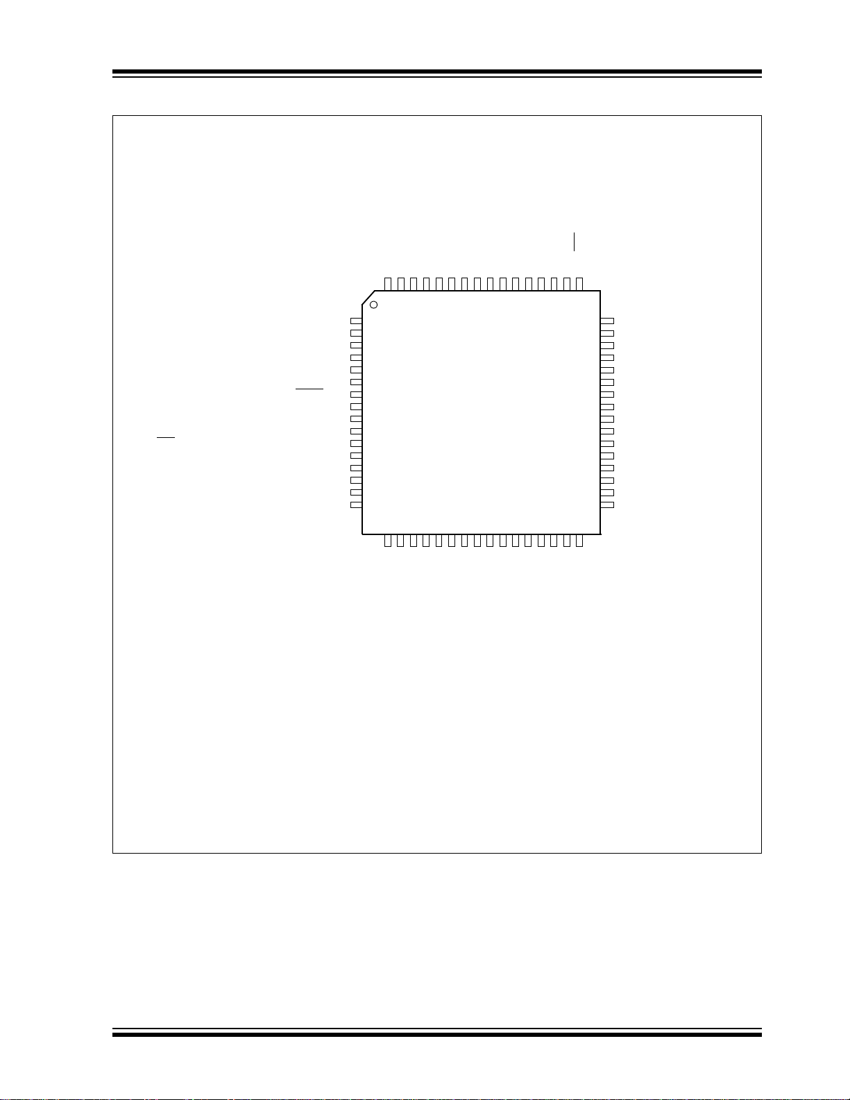
Pin Diagram – 64-Pin TQFP/QFN (PIC16F/LF1946/47)
1
2
3
4
5
6
7
8
9
10
11
12
13
14
38
37
36
35
34
33
50 49
17 18 19 20 21 22 23 24 25 26
RE2/P2B
(1)
/VLCD3
RE3/P3C
(1)
/COM0
RE4/P3B
(1)
/COM1
RE5/P1C
(1)
/COM2
RE6/P1B
(1)
/COM3
RE7/CCP2
(2)
/P2A
(2)
/SEG31
RD0/P2D
(2)
/SEG0
V
DD
VSS
RD1/P2C
(2)
/SEG1
RD2/P2B
(2)
/SEG2
RD3/P3C
(2)
/SEG3
RD4/SDO2/P3B
(2)
/SEG4
RD5/SDI2/SDA2/P1C
(2)
/SEG5
RD6/SCK2/SCL2/P1B
(2)
/SEG6
RD7/SS2
/SEG7
VLCD2/P2C
(1)
/RE1
VLCD1/P2D
(1)
/RE0
SEG42/P3A/CCP3/RG0
SEG43/C3OUT/CK2/TX2/CPS15/AN15/RG1
SEG44/C3IN+/DT2/RX2/CPS14/AN14/RG2
SEG45/P3D/CCP4/C3IN0-/CPS13/AN13/RG3
V
PP/MCLR/RG5
SEG26/P1D/CCP5/C3IN1-/CPS12/AN12/RG4
V
SS
VDD
SEG25/SS1/C1IN3-/C2IN3-/C3IN3-/CPS5/AN5/RF7
SEG24/C1IN+/CPS11/AN11/RF6
SEG23/DACOUT/C1IN1-/C2IN1-/CPS10/AN10/RF5
SEG22/C2IN+/CPS9/AN9/RF4
SEG21/C1IN2-/C2IN2-/C3IN2-/CPS8/AN8/RF3
SEG20/SRQ/C1OUT/CPS7/AN7/RF2
RB0/INT/SRI/FLT0/SEG30
RB1/SEG8
RB2/SEG9
RB3/SEG10
RB4/SEG11
RB5/T1G/SEG29
RB6/ICSPCLK/ICDCLK/SEG38
V
SS
RA6/OSC2/CLKOUT/SEG36
RA7/OSC1/CLKIN/SEG37
V
DD
RB7/ICSPDAT/ICDDAT/SEG39
RC4/SDI1/SDA1/SEG16
RC3/SCK1/SCL1/SEG17
RC2/CCP1/P1A/SEG13
VCAP/SEG41/C1IN0-/C2IN0-/CPS16/AN16/RF0
SEG19/SRNQ/C2OUT/CPS6/AN6/RF1
AV
DD
AVSS
SEG35/CPS3/VREF+/AN3/RA3
SEG34/CPS2/V
REF-/AN2/RA2
SEG18/CPS1/AN1/RA1
SEG33/CPS0/AN0/RA0
V
SS
VDD
SEG14/T0CKI/RA4
SEG15/CPS4/AN4/RA5
SEG32/CCP2
(1)
/P2A
(1)/
/T1OSI/RC1
SEG40/T1CKI/T1OSO/RC0
SEG28/DT1/RX1/RC7
SEG27/CK1/TX1/RC6
RC5/SDO1/SEG12
15
16
31
40
39
27 28
29 30 32
48
47
46
45
44
43
42
41
54 53 52 5158 57 56 5560 59
64
63 62 61
64-pin TQFP, QFN
Note 1: Pin location selected by APFCON register setting. Default location.
2: Pin function can be moved using the APFCON register. Alternate location.
3: QFN package orientation is the same. No leads are present on the QFN package.
PIC16F/LF1946/47
PIC16F/LF1946/47
2010 Microchip Technology Inc. Preliminary DS41414B-page 5
PIC16F/LF1946/47
TABLE 1: 64-PIN SUMMARY(PIC16F/LF1946/47)
I/O
64-Pin TQFP, QFN
RA0 24 Y AN0 — CPS0 — — — — — — SEG33 — — —
RA1 23 Y AN1 — CPS1 — — — — — — SEG18 — — —
RA2 22 Y AN2 VREF- CPS2 — — — — — — SEG34 — — —
RA3 21 Y AN3 V
RA4 28 — — — — — — T0CKI — — — SEG14 — — —
RA5 27 Y AN4 — CPS4 — — — — — — SEG15 — — —
RA6 40 — — — — — — — — — — SEG36 — — OSC2/
RA739——— ———— — ——SEG37——OSC1/
RB0 48 — — — — — SRI — FLT0 — — SEG30 INT/
RB147——— ———— — ——SEG8IOCY —
RB2 46 — — — — — — — — — — SEG9 IOC Y —
RB345——— ———— — ——SEG10IOCY —
RB4 44 — — — — — — — — — — SEG11 IOC Y —
RB543——— ———T1G— ——SEG29IOCY —
RB6 42 — — — — — — — — — — SEG38 IOC Y ICSP-
RB7 37 — — — — — — — — — — SEG39 IOC Y ICSP-
RC0 30 — — — — — — T1OSO/
RC1 29 — — — — — — T1OSI CCP2
RC2 33 — — — — — — — CCP1/
RC334—————————SCK1/
RC4 35 — — — — — — — — — SDI1/
RC536——— ———— — —SDO1SEG12———
RC6 31 — — — — — — — — TX1/
RC732——— ———— —RX1/
RD0 58 — — — — — — — P2D
RD155——— ————P2C
RD2 54 — — — — — — — P2B
RD353——— ————
RD4 52 — — — — — — — P3B
RD551——— ————P1C
RD6 50 — — — — — — — P1B
ANSEL
A/D
Reference
REF+ CPS3 — — — — — — SEG35 — — —
Cap Sense
Comparator
SR Latch
Timers
T1CKI
CCP
— — — SEG40 — — —
(1)
(1)
P2A
P1A
(2)
(2)
(2)
(2)
P3C
(2)
(2)
(2)
USART
/
— — SEG32 — — —
— — SEG13 — — —
SCL1
SDA1
CK1
DT1
— SEG27 — — —
— SEG28 — — —
— — SEG0 — — —
— — SEG1 — — —
— — SEG2 — — —
— — SEG3 — — —
— SDO2 SEG4 — — —
—SDI2
SDA2
— SCK2/
SCL2
LCD
MSSP
SEG17 — — —
SEG16 — — —
SEG5 — — —
SEG6 — — —
Interrupt
IOC
Pull-up
CLKOUT
CLKIN
Y —
CLK/
ICDCLK
DAT/
ICDDAT
Basic
Note 1: Pin functions can be moved using the APFCON register(s). Default location.
2: Pin function can be moved using the APFCON register. Alternate location.
3: Weak pull-up always enabled when MCLR
is enabled, otherwise the pull-up is under user control.
4: See Section 8.0.
DS41414B-page 6 Preliminary 2010 Microchip Technology Inc.
PIC16F/LF1946/47
TABLE 1: 64-PIN SUMMARY(PIC16F/LF1946/47) (Continued)
I/O
64-Pin TQFP, QFN
RD749—————————SS2SEG7 — — —
RE0 2 Y — — — — — — P2D
RE11Y—— ————P2C
RE2 64 Y — — — — — — P2B
RE363——— ————P3C
RE4 62 — — — — — — — P3B
RE561——— ————P1C
RE6 60 — — — — — — — P1B
RE759——— ————
RF0 18 Y AN16 — CPS16 C1IN0-
RF1 17 Y AN6 — CPS6 C2OUT SRNQ —
RF2 16 Y AN7 — CPS7 C1OUT SRQ — — — — SEG20 — — —
RF3 15 Y AN8 CPS8 C1IN2-
RF4 14 Y AN9 — CPS9 C2IN+ — — — — — SEG22 — — —
RF5 13 Y AN10 DACOUT CPS10 C1IN1-
RF6 12 Y AN11 — CPS11 C1IN+ — — — — — SEG24 — — —
RF7 11 Y AN5 — CPS5 C1IN3-
RG0 3 — — — — — — — CCP3
RG1 4 Y AN15 — CPS15 C3OUT — — — TX2/
RG2 5 Y AN14 — CPS14 C3IN+ — — — RX2/
RG3 6 Y AN13 — CPS13 C3IN0- — — CCP4
RG4 8 Y AN12 — CPS12 C3IN1- — — CCP5
RG57————————————
VDD 10
26
38
57
VSS 9
25
41
56
AVDD 19 — — — — — — — — — — — — — AVDD
AVSS 20——— ———— — —————AVSS
A/D
ANSEL
— — — — — — — — — — — — — VDD
——— ———— — —————VSS
Reference
Cap Sense
Comparator
C2IN0-
C2IN2C3IN2-
C2IN1-
C2IN3C3IN3-
SR Latch
— — — — — SEG41 — — VCAP
—— — ——SEG21———
—
————SS1
Timers
CCP2
P2A
—
—
P3A
P3D
P1D
CCP
(1)
(1)
(1)
(1)
(1)
(1)
(1)
(2)
(2)
USART
— VLCD1 — — —
——VLCD2———
— — VLCD3 — — —
——COM0———
— — COM1 — — —
——COM2———
— — COM3 — — —
/
— — SEG31 — — —
— — SEG19 — — —
— — SEG23 — — —
— — SEG42 — — —
CK2
DT2
— SEG43 — — —
— SEG44 — — —
——
— — SEG26 — — —
LCD
MSSP
SEG25 — — —
SEG45
Interrupt
———
Y
Pull-up
(2)
MCLR/
PP
V
Note 1: Pin functions can be moved using the APFCON register(s). Default location.
2: Pin function can be moved using the APFCON register. Alternate location.
3: Weak pull-up always enabled when MCLR
is enabled, otherwise the pull-up is under user control.
4: See Section 8.0.
Basic
(3)
2010 Microchip Technology Inc. Preliminary DS41414B-page 7

PIC16F/LF1946/47
Table of Contents
1.0 Device Overview ........................................................................................................................................................................ 11
2.0 Enhanced Mid-Range CPU ........................................................................................................................................................ 19
3.0 Memory Organization ................................................................................................................................................................. 21
4.0 Device Configuration.................................................................................................................................................................. 55
5.0 Oscillator Module (With Fail-Safe Clock Monitor)....................................................................................................................... 61
6.0 Resets ........................................................................................................................................................................................ 79
7.0 Interrupts .................................................................................................................................................................................... 87
8.0 Low Dropout (LDO) Voltage Regulator .................................................................................................................................... 103
9.0 Power-Down Mode (Sleep) ...................................................................................................................................................... 105
10.0 Watchdog Timer ....................................................................................................................................................................... 107
11.0 Data EEPROM and Flash Program Memory Control ............................................................................................................... 111
12.0 I/O Ports ................................................................................................................................................................................... 125
13.0 Interrupt-On-Change ................................................................................................................................................................ 151
14.0 Fixed Voltage Reference (FVR) ............................................................................................................................................... 155
15.0 Temperature Indicator Module ................................................................................................................................................. 157
16.0 Analog-to-Digital Converter (ADC) Module .............................................................................................................................. 159
17.0 Digital-to-Analog Converter (DAC) Module .............................................................................................................................. 173
18.0 Comparator Module.................................................................................................................................................................. 177
19.0 SR Latch................................................................................................................................................................................... 187
20.0 Timer0 Module ......................................................................................................................................................................... 193
21.0 Timer1 Module with Gate Control............................................................................................................................................. 197
22.0 Timer2/4/6 Modules.................................................................................................................................................................. 209
23.0 Capture/Compare/PWM Modules ............................................................................................................................................ 213
24.0 Master Synchronous Serial Port (MSSP1 and MSSP2) Module .............................................................................................. 243
25.0 Enhanced Universal Synchronous Asynchronous Receiver Transmitter (EUSART) ............................................................... 297
26.0 Capacitive Sensing (CPS) Module ........................................................................................................................................... 325
27.0 Liquid Crystal Display (LCD) Driver Module ............................................................................................................................. 335
28.0 In-Circuit Serial Programming™ (ICSP™) ............................................................................................................................... 371
29.0 Instruction Set Summary.......................................................................................................................................................... 375
30.0 Electrical Specifications............................................................................................................................................................ 389
31.0 DC and AC Characteristics Graphs and Charts ....................................................................................................................... 423
32.0 Development Support............................................................................................................................................................... 425
33.0 Packaging Information.............................................................................................................................................................. 429
Appendix A: Data Sheet Revision History .......................................................................................................................................... 435
Appendix B: Migrating From Other PIC
Index .................................................................................................................................................................................................. 437
The Microchip Web Site..................................................................................................................................................................... 445
Customer Change Notification Service .............................................................................................................................................. 445
Customer Support .............................................................................................................................................................................. 445
Reader Response .............................................................................................................................................................................. 446
Product Identification System............................................................................................................................................................. 447
®
Devices.............................................................................................................................. 435
DS41414B-page 8 Preliminary 2010 Microchip Technology Inc.

PIC16F/LF1946/47
TO OUR VALUED CUSTOMERS
It is our intention to provide our valued customers with the best documentation possible to ensure successful use of your Microchip
products. To this end, we will continue to improve our publications to better suit your needs. Our publications will be refined and
enhanced as new volumes and updates are introduced.
If you have any questions or comments regarding this publication, please contact the Marketing Communications Department via
E-mail at docerrors@microchip.com or fax the Reader Response Form in the back of this data sheet to (480) 792-4150. We
welcome your feedback.
Most Current Data Sheet
To obtain the most up-to-date version of this data sheet, please register at our Worldwide Web site at:
http://www.microchip.com
You can determine the version of a data sheet by examining its literature number found on the bottom outside corner of any page.
The last character of the literature number is the version number, (e.g., DS30000A is version A of document DS30000).
Errata
An errata sheet, describing minor operational differences from the data sheet and recommended workarounds, may exist for current
devices. As device/documentation issues become known to us, we will publish an errata sheet. The errata will specify the revision
of silicon and revision of document to which it applies.
To determine if an errata sheet exists for a particular device, please check with one of the following:
• Microchip’s Worldwide Web site; http://www.microchip.com
• Your local Microchip sales office (see last page)
When contacting a sales office, please specify which device, revision of silicon and data sheet (include literature number) you are
using.
Customer Notification System
Register on our web site at www.microchip.com to receive the most current information on all of our products.
2010 Microchip Technology Inc. Preliminary DS41414B-page 9

PIC16F/LF1946/47
NOTES:
DS41414B-page 10 Preliminary 2010 Microchip Technology Inc.
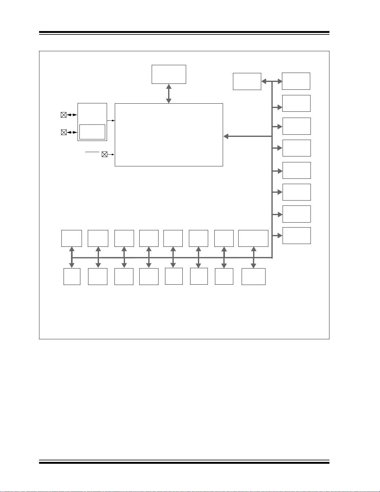
1.0 DEVICE OVERVIEW
The PIC16F/LF1946/47 are described within this data
sheet. They are available in 64-pin packages.
Figure 1-1 shows a block diagram of the
PIC16F/LF1946/47 devices. Ta bl e 1 - 2 shows the pinout descriptions.
Reference Tab le 1 -1 for peripherals available per
device.
TABLE 1-1: DEVICE PERIPHERAL
SUMMARY
Peripheral
PIC16F/LF1946/47
PIC16F1946/47
ADC ●●
Capacitive Sensing (CPS) Module ●●
Data EEPROM ●●
Digital-to-Analog Converter (DAC) ●●
Fixed Voltage Reference (FVR) ●●
LCD ●●
SR Latch ●●
Capture/Compare/PWM Modules
ECCP1 ●●
ECCP2 ●●
ECCP3 ●●
CCP4 ●●
CCP5 ●●
Comparators
C1 ●●
C2 ●●
C3 ●●
EUSARTS
EUSART1 ●●
EUSART2 ●●
Master Synchronous Serial Ports
MSSP1 ●●
MSSP2 ●●
Timers
Timer0 ●●
Timer1 ●●
Timer2 ●●
Timer4 ●●
Timer6 ●●
PIC16LF1946/47
2010 Microchip Technology Inc. Preliminary DS41414B-page 11
PIC16F/LF1946/47
PORTA
EUSARTx
Comparators
MSSPx
Timer2Timer1 Timer4Timer0
ECCP1
ADC
10-Bit
ECCP2 ECCP3
CCP4 CCP5
Timer6
PORTB
PORTC
PORTD
PORTE
LCD
SR
Latch
Note 1: See applicable chapters for more information on peripherals.
CPU
Program
Flash Memory
EEPROM
RAM
Timing
Generation
INTRC
Oscillator
MCLR
Figure 2-1
OSC1/CLKIN
OSC2/CLKOUT
PORTF
PORTG
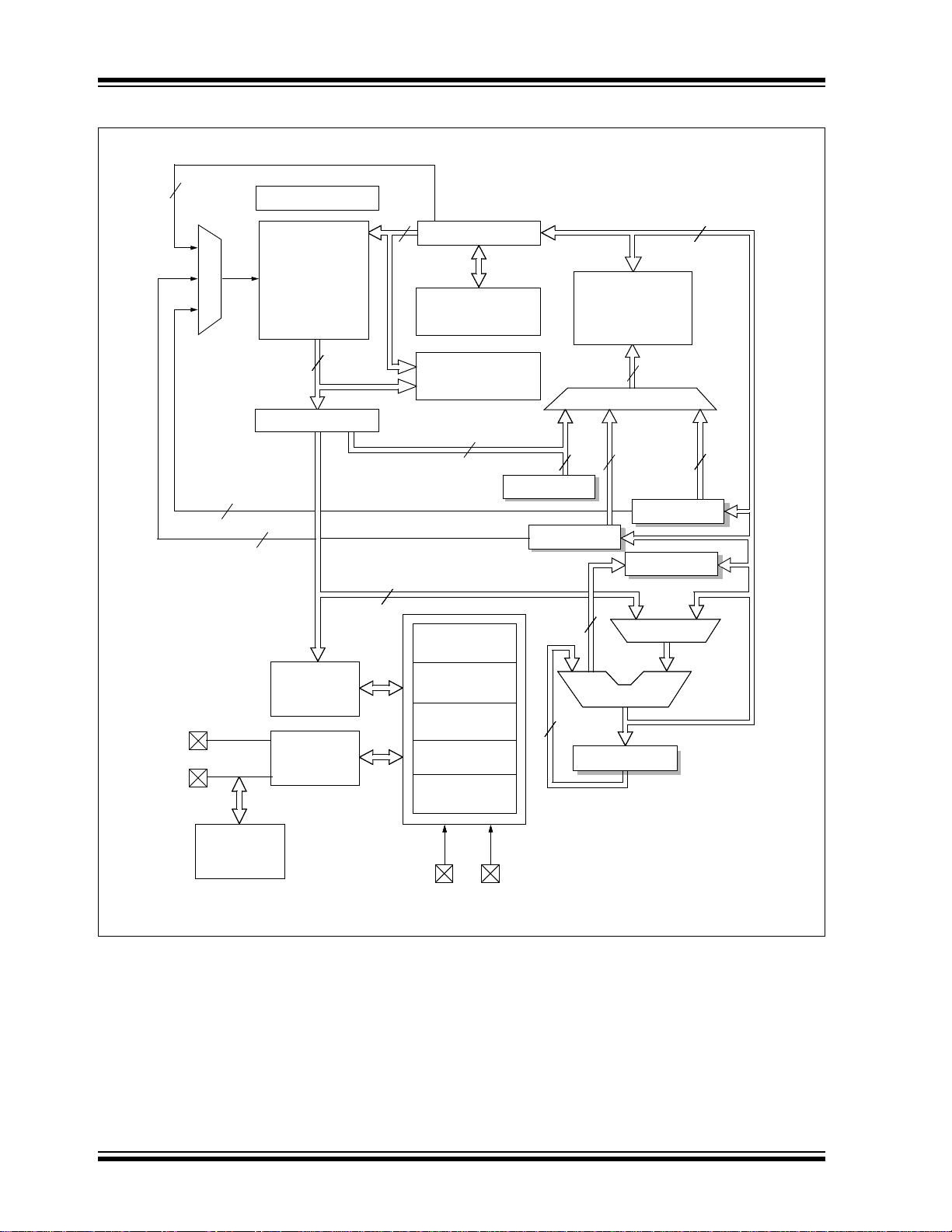
FIGURE 1-1: PIC16F/LF1946/47 BLOCK DIAGRAM
DS41414B-page 12 Preliminary 2010 Microchip Technology Inc.
PIC16F/LF1946/47
TABLE 1-2: PIC16F/LF1946/47 PINOUT DESCRIPTION
Input
Name Function
RA0/AN0/CPS0/SEG33 RA0 TTL CMOS General purpose I/O.
AN0 AN — A/D Channel 0 input.
CPS0 AN — Capacitive sensing input 0.
SEG33 — AN LCD Analog output.
RA1/AN1/CPS1/SEG18 RA1 TTL CMOS General purpose I/O.
AN1 AN — A/D Channel 1 input.
CPS1 AN — Capacitive sensing input 1.
SEG18 — AN LCD Analog output.
RA2/AN2/V
RA3/AN3/V
RA4/T0CKI/SEG14 RA4 TTL CMOS General purpose I/O.
RA5/AN4/CPS4/SEG15 RA5 TTL CMOS General purpose I/O.
RA6/OSC2/CLKOUT/SEG36 RA6 TTL CMOS General purpose I/O.
RA7/OSC1/CLKIN/SEG37 RA7 TTL CMOS General purpose I/O.
RB0/INT/SRI/FLT0/SEG30 RB0 TTL CMOS General purpose I/O. Individually controlled interrupt-on-change.
RB1/SEG8 RB1 TTL CMOS General purpose I/O. Individually controlled interrupt-on-change.
Legend: AN = Analog input or output CMOS= CMOS compatible input or output OD = Open Drain
Note 1: Pin function is selectable via the APFCON register.
REF-/CPS2/SEG34 RA2 TTL CMOS General purpose I/O.
AN2 AN — A/D Channel 2 input.
REF- AN — A/D Negative Voltage Reference input.
V
CPS2 AN — Capacitive sensing input 2.
SEG34 — AN LCD Analog output.
REF+/CPS3/SEG35 RA3 TTL CMOS General purpose I/O.
AN3 AN — A/D Channel 3 input.
REF+ AN — A/D Voltage Reference input.
V
CPS3 AN — Capacitive sensing input 3.
SEG35 — AN LCD Analog output.
T0CKI ST — Timer0 clock input.
SEG14 — AN LCD Analog output.
AN4 AN — A/D Channel 4 input.
CPS4 AN — Capacitive sensing input 4.
SEG5 — AN LCD Analog output.
OSC2 — XTAL Crystal/Resonator (LP, XT, HS modes).
CLKOUT — CMOS F
SEG36 — AN LCD Analog output.
OSC1 XTAL — Crystal/Resonator (LP, XT, HS modes).
CLKIN CMOS — External clock input (EC mode).
SEG37 — AN LCD Analog output.
INT ST — External interrupt.
SRI — ST SR Latch input.
FLT0 ST — ECCP Auto-shutdown Fault input.
SEG30 — AN LCD analog output.
SEG8 — AN LCD Analog output.
TTL = TTL compatible input ST = Schmitt Trigger input with CMOS levels I
HV = High Voltage XTAL = Crystal levels
Type
Output
Type
OSC/4 output.
Individually enabled pull-up.
Individually enabled pull-up.
Description
2
C™ = Schmitt Trigger input with I2C
2010 Microchip Technology Inc. Preliminary DS41414B-page 13
PIC16F/LF1946/47
TABLE 1-2: PIC16F/LF1946/47 PINOUT DESCRIPTION (CONTINUED)
Input
Name Function
RB2/SEG9 RB2 TTL CMOS General purpose I/O. Individually controlled interrupt-on-change.
SEG9 — AN LCD Analog output.
RB3/SEG10 RB3 TTL CMOS General purpose I/O. Individually controlled interrupt-on-change.
SEG10 — AN LCD Analog output.
RB4/SEG11 RB4 TTL CMOS General purpose I/O. Individually controlled interrupt-on-change.
SEG11 — AN LCD Analog output.
RB5/T1G/SEG29 RB5 TTL CMOS General purpose I/O. Individually controlled interrupt-on-change.
T1G ST — Timer1 Gate input.
SEG29 — AN LCD Analog output.
RB6/ICSPCLK/ICDCLK/SEG38 RB6 TTL CMOS General purpose I/O. Individually controlled interrupt-on-change.
ICSPCLK ST — Serial Programming Clock.
ICDCLK ST — In-Circuit Debug Clock.
SEG38 — AN LCD Analog output.
RB7/ICSPDAT/ICDDAT/SEG39 RB7 TTL CMOS General purpose I/O. Individually controlled interrupt-on-change.
ICSPDAT ST CMOS ICSP™ Data I/O.
ICDDAT ST CMOS In-Circuit Data I/O.
SEG39 — AN LCD Analog output.
RC0/T1OSO/T1CKI/SEG40 RC0 ST CMOS General purpose I/O.
T1OSO XTAL XTAL Timer1 oscillator connection.
T1CKI ST — Timer1 clock input.
RC1/T1OSI/P2A
SEG32
RC2/CCP1/P1A/SEG13 RC2 ST CMOS General purpose I/O.
RC3/SCK/SCL/SEG17 RC3 ST CMOS General purpose I/O.
RC4/SDI1/SDA1/SEG16 RC4 ST CMOS General purpose I/O.
Legend: AN = Analog input or output CMOS= CMOS compatible input or output OD = Open Drain
Note 1: Pin function is selectable via the APFCON register.
(1)
TTL = TTL compatible input ST = Schmitt Trigger input with CMOS levels I
HV = High Voltage XTAL = Crystal levels
/CCP2
(1)
/
SEG40 — AN LCD Analog output.
RC1 ST CMOS General purpose I/O.
T1OSI XTAL XTAL Timer1 oscillator connection.
P2A — CMOS PWM output.
CCP2 ST CMOS Capture/Compare/PWM2.
SEG32 — AN LCD Analog output.
CCP1 ST CMOS Capture/Compare/PWM1.
P1A — CMOS PWM output.
SEG13 — AN LCD Analog output.
SCK ST CMOS SPI clock.
SCL I
SEG17 — AN LCD Analog output.
SDI1 ST — SPI data input.
SDA1 I
SEG16 — AN LCD Analog output.
Output
Type
Type
Individually enabled pull-up.
Individually enabled pull-up.
Individually enabled pull-up.
Individually enabled pull-up.
Individually enabled pull-up.
Individually enabled pull-up.
2
CODI2C™ clock.
2
CODI2C™ data input/output.
Description
2
C™ = Schmitt Trigger input with I2C
DS41414B-page 14 Preliminary 2010 Microchip Technology Inc.
PIC16F/LF1946/47
TABLE 1-2: PIC16F/LF1946/47 PINOUT DESCRIPTION (CONTINUED)
Input
Name Function
RC5/SDO1/SEG12 RC5 ST CMOS General purpose I/O.
SDO1 — CMOS SPI data output.
SEG12 — AN LCD Analog output.
RC6/TX1/CK1/SEG27 RC6 ST CMOS General purpose I/O.
TX1 — CMOS USART1 asynchronous transmit.
CK1 ST CMOS USART1 synchronous clock.
SEG27 — AN LCD Analog output.
RC7/RX1/DT1/SEG28 RC7 ST CMOS General purpose I/O.
RX ST — USART1 asynchronous input.
DT1 ST CMOS USART1 synchronous data.
SEG28 — AN LCD Analog output.
(1)
RD0/P2D
/SEG0 RD0 ST CMOS General purpose I/O.
P2D — CMOS PWM output.
SEG0 — AN LCD Analog output.
(1)
RD1/P2C
/SEG1 RD1 ST CMOS General purpose I/O.
P2C — CMOS PWM output.
SEG1 — AN LCD Analog output.
(1)
RD2/P2B
/SEG2 RD2 ST CMOS General purpose I/O.
P2B — CMOS PWM output.
SEG2 — AN LCD Analog output.
(1)
RD3/P3C
/SEG3 RD3 ST CMOS General purpose I/O.
P3C — CMOS PWM output.
SEG3 — AN LCD analog output.
(1)
RD4/SDO2/P3B
/SEG4 RD4 ST CMOS General purpose I/O.
SDO2 — CMOS SPI data output.
P3B — CMOS PWM output.
SEG4 — AN LCD analog output.
(1)
RD5/SDI2/SDA2/P1C
/SEG5 RD5 ST CMOS General purpose I/O.
SDI2 ST — SPI data input.
SDA2 I
P1C — CMOS PWM output.
SEG5 — AN LCD analog output.
(1)
RD6/SCK2/SCL2/P1B
/SEG6 RD6 ST CMOS General purpose I/O.
SCK2 ST CMOS SPI clock.
SCL2 I
P1B — CMOS PWM output.
SEG6 — AN LCD analog output.
RD7/SS2
/SEG7 RD7 ST CMOS General purpose I/O.
SS2
SEG7 — AN LCD analog output.
(1)
RE0/P2D
/VLCD1 RE0 ST CMOS General purpose I/O.
P2D — CMOS PWM output.
VLCD1 AN — LCD analog input.
Legend: AN = Analog input or output CMOS= CMOS compatible input or output OD = Open Drain
TTL = TTL compatible input ST = Schmitt Trigger input with CMOS levels I
HV = High Voltage XTAL = Crystal levels
Note 1: Pin function is selectable via the APFCON register.
Output
Type
Type
2
CODI2C™ data input/output.
2
CODI2C™ clock.
ST — Slave Select input.
Description
2
C™ = Schmitt Trigger input with I2C
2010 Microchip Technology Inc. Preliminary DS41414B-page 15
PIC16F/LF1946/47
TABLE 1-2: PIC16F/LF1946/47 PINOUT DESCRIPTION (CONTINUED)
Input
Name Function
RE1/P2C
(1)
/VLCD2 RE1 ST CMOS General purpose I/O.
P2C — CMOS PWM output.
VLCD2 AN — LCD analog input.
(1)
RE2/P2B
/VLCD3 RE2 ST CMOS General purpose I/O.
P2B — CMOS PWM output.
VLCD3 AN — LCD analog input.
(1)
RE3/P3C
/COM0 RE3 TTL — General purpose input.
P3C — CMOS PWM output.
COM0 — AN LCD Analog output.
(1)
RE4/P3B
/COM1 RE4 TTL — General purpose input.
P3B — CMOS PWM output.
COM1 — AN LCD Analog output.
(1)
RE5/P1C
/COM2 RE5 TTL — General purpose input.
P1C — CMOS PWM output.
COM2 — AN LCD Analog output.
(1)
RE6/P1B
/COM3 RE6 TTL — General purpose input.
P1B — CMOS PWM output.
COM3 — AN LCD Analog output.
(1)
(1)
/P2A
RE7/CCP2
/SEG31 RE7 TTL — General purpose input.
CCP2 ST CMOS Capture/Compare/PWM2.
P2A — CMOS PWM output.
SEG31 — AN LCD analog output.
RF0/AN16/CPS16/C12IN0-/
SEG41/V
CAP
RF0 TTL CMOS General purpose I/O.
AN16 AN — A/D Channel 16 input.
CPS16 AN — Capacitive sensing input 16.
C1IN0-
C2IN0-
SEG41 — AN LCD Analog output.
V
CAP Power Power Filter capacitor for Voltage Regulator.
RF1/AN6/CPS6/C2OUT/SRNQ/
SEG19
RF1 TTL CMOS General purpose I/O.
AN6 AN — A/D Channel 6 input.
CPS6 AN — Capacitive sensing input 6.
C2OUT — CMOS Comparator C2 output.
SRNQ — CMOS SR Latch inverting output.
SEG19 — AN LCD Analog output.
RF2/AN7/CPS7/C1OUT/SRQ/
SEG20
RF2 TTL CMOS General purpose I/O.
AN7 AN — A/D Channel 7 input.
CPS7 AN — Capacitive sensing input 7.
C1OUT — CMOS Comparator C1 output.
SRQ
SEG20 — AN LCD Analog output.
Legend: AN = Analog input or output CMOS= CMOS compatible input or output OD = Open Drain
TTL = TTL compatible input ST = Schmitt Trigger input with CMOS levels I
HV = High Voltage XTAL = Crystal levels
Note 1: Pin function is selectable via the APFCON register.
Output
Type
Type
AN — Comparator C1 negative input.
AN — Comparator C2 negative input.
CMOS SR Latch non-inverting output.
—
Description
2
C™ = Schmitt Trigger input with I2C
DS41414B-page 16 Preliminary 2010 Microchip Technology Inc.
PIC16F/LF1946/47
TABLE 1-2: PIC16F/LF1946/47 PINOUT DESCRIPTION (CONTINUED)
Input
Name Function
RF3/AN8/CPS8/C123IN2-/
SEG21
RF4/AN9/CPS9/C2IN+/SEG22 RF4 TTL CMOS General purpose I/O.
RF5/AN10/CPS10/C12IN1-/
DACOUT/SEG23
RF6/AN11/CPS11/C1IN+/SEG24 RF6 TTL CMOS General purpose I/O.
RF7/AN5/CPS5/C123IN3-/SS1
SEG25
RG0/CCP3/P3A/SEG42 RG0 ST CMOS General purpose I/O.
RG1/AN15/CPS15/TX2/CK2/
C3OUT/SEG43
Legend: AN = Analog input or output CMOS= CMOS compatible input or output OD = Open Drain
TTL = TTL compatible input ST = Schmitt Trigger input with CMOS levels I
HV = High Voltage XTAL = Crystal levels
Note 1: Pin function is selectable via the APFCON register.
RF3 TTL CMOS General purpose I/O.
AN8 AN — A/D Channel 8 input.
CPS8 AN — Capacitive sensing input 8.
C1IN2-
C2IN2-
C3IN2-
SEG21 — AN LCD Analog output.
AN9 AN — A/D Channel 9 input.
CPS9 AN — Capacitive sensing input 9.
C2IN+
SEG22 — AN LCD Analog output.
RF5 TTL CMOS General purpose I/O.
AN10 AN — A/D Channel 10 input.
CPS10 AN — Capacitive sensing input 10.
C1IN1-
C2IN1-
DACOUT — AN Voltage Reference output.
SEG23 — AN LCD Analog output.
AN11 AN — A/D Channel 11 input.
CPS11 AN — Capacitive sensing input 11.
C1IN+
SEG24 — AN LCD Analog output.
/
RF7 TTL CMOS General purpose I/O.
AN5 AN — A/D Channel 5 input.
CPS5 AN — Capacitive sensing input 5.
C1IN3-
C2IN3-
C3IN3-
SS1 ST — Slave Select input.
SEG25 — AN LCD Analog output.
CCP3 ST CMOS Capture/Compare/PWM3.
P3A — CMOS PWM output.
SEG42 — AN LCD Analog output.
RG1 ST CMOS General purpose I/O.
AN15 AN — A/D Channel 15 input.
CPS15 AN — Capacitive sensing input 15.
TX2 — CMOS USART2 asynchronous transmit.
CK2 ST CMOS USART2 synchronous clock.
C3OUT — CMOS Comparator C3 output.
SEG43 — AN LCD Analog output.
Output
Type
Type
AN — Comparator C1 negative input.
AN — Comparator C2 negative input.
AN — Comparator C3 negative input.
AN — Comparator C2 positive input.
AN — Comparator C1 negative input.
AN — Comparator C2 negative input.
AN — Comparator C1 positive input.
AN — Comparator C1negative input.
AN — Comparator C2 negative input.
AN — Comparator C3 negative input.
Description
2
C™ = Schmitt Trigger input with I2C
2010 Microchip Technology Inc. Preliminary DS41414B-page 17
PIC16F/LF1946/47
TABLE 1-2: PIC16F/LF1946/47 PINOUT DESCRIPTION (CONTINUED)
Input
Name Function
RG2/AN14/CPS14/RX2/DT2/
C3IN+/SEG44
RG3/AN13/CPS13/C3IN0-/
CCP4/P3D/SEG45
RG4/AN12/CPS12/C3IN1-/
CCP5/P1D/SEG26
RG5/MCLR
DD VDD Power — Positive supply.
V
V
SS VSS Power — Ground reference.
Legend: AN = Analog input or output CMOS= CMOS compatible input or output OD = Open Drain
Note 1: Pin function is selectable via the APFCON register.
/VPP RG5 TTL — General purpose input.
TTL = TTL compatible input ST = Schmitt Trigger input with CMOS levels I
HV = High Voltage XTAL = Crystal levels
RG2 ST CMOS General purpose I/O.
AN14 AN — A/D Channel 14 input.
CPS14 AN — Capacitive sensing input 14.
RX2 ST — USART2 asynchronous input.
DT2 ST CMOS USART2 synchronous data.
C3IN+
SEG44 — AN LCD Analog output.
RG3 ST CMOS General purpose I/O.
AN13 AN — A/D Channel 13 input.
CPS13 AN — Capacitive sensing input 13.
C3IN0-
CCP4 ST CMOS Capture/Compare/PWM4.
P3D — CMOS PWM output.
SEG45 — AN LCD Analog output.
RG4 ST CMOS General purpose I/O.
AN12 AN — A/D Channel 12 input.
CPS12 AN — Capacitive sensing input 12.
C3IN1-
CCP5 ST CMOS Capture/Compare/PWM5.
P1D — CMOS PWM output.
SEG26 — AN LCD Analog output.
MCLR
PP HV — Programming voltage.
V
Output
Type
Type
AN — Comparator C3 positive input.
AN — Comparator C3 negative input.
AN — Comparator C3 negative input.
ST — Master Clear with internal pull-up.
Description
2
C™ = Schmitt Trigger input with I2C
DS41414B-page 18 Preliminary 2010 Microchip Technology Inc.

2.0 ENHANCED MID-RANGE CPU
This family of devices contain an enhanced mid-range
8-bit CPU core. The CPU has 49 instructions. Interrupt
capability includes automatic context saving. The
hardware stack is 16 levels deep and has Overflow and
Underflow Reset capability. Direct, Indirect, and
Relative addressing modes are available. Two File
Select Registers (FSRs) provide the ability to read
program and data memory.
• Automatic Interrupt Context Saving
• 16-level Stack with Overflow and Underflow
• File Select Registers
• Instruction Set
2.1 Automatic Interrupt Context Saving
During interrupts, certain registers are automatically
saved in shadow registers and restored when returning
from the interrupt. This saves stack space and user
code. See Section 7.5 “Automatic Context Saving”,
for more information.
PIC16F/LF1946/47
2.2 16-level Stack with Overflow and Underflow
These devices have an external stack memory 15 bits
wide and 16 words deep. A Stack Overflow or Underflow will set the appropriate bit (STKOVF or STKUNF)
in the PCON register, and if enabled will cause a software Reset. See section Section 3.4 “St ack” for more
details.
2.3 File Select Registers
There are two 16-bit File Select Registers (FSR). FSRs
can access all file registers and program memory,
which allows one data pointer for all memory. When an
FSR points to program memory, there is 1 additional
instruction cycle in instructions using INDF to allow the
data to be fetched. General purpose memory can now
also be addressed linearly, providing the ability to
access contiguous data larger than 80 bytes. There are
also new instructions to support the FSRs. See
Section 3.5 “Indirect Addressing” for more details.
2.4 Instruction Set
There are 49 instructions for the enhanced mid-range
CPU to support the features of the CPU. See
Section 29.0 “Instruction Set Summary” for more
details.
2010 Microchip Technology Inc. Preliminary DS41414B-page 19
PIC16F/LF1946/47
Data Bus
8
14
Program
Bus
Instruction reg
Program Counter
8 Level Stack
(13-bit)
Direct Addr
7
12
Addr MUX
FSR reg
STATUS reg
MUX
ALU
Power-up
Timer
Oscillator
Start-up Timer
Power-on
Reset
Watchdog
Timer
Instruction
Decode &
Control
Timing
Generation
OSC1/CLKIN
OSC2/CLKOUT
V
DD
8
8
Brown-out
Reset
12
3
VSS
Internal
Oscillator
Block
Configuration
Data Bus
8
14
Program
Bus
Instruction reg
Program Counter
8 Level Stack
(13-bit)
Direct Addr
7
Addr MUX
FSR reg
STATUS reg
MUX
ALU
W Reg
Instruction
Decode &
Control
Timing
Generation
V
DD
8
8
3
VSS
Internal
Oscillator
Block
Configuration
15
Data Bus
8
14
Program
Bus
Instruction Reg
Program Counter
16-Level Stack
(15-bit)
Direct Addr
7
RAM Addr
Addr MUX
Indirect
Addr
FSR0 Reg
STATUS Reg
MUX
ALU
Instruction
Decode and
Control
Timing
Generation
V
DD
8
8
3
VSS
Internal
Oscillator
Block
Configuration
Flash
Program
Memory
RAM
FSR regFSR reg
FSR1 Reg
15
15
MUX
15
Program Memory
Read (PMR)
12
FSR regFSR reg
BSR Reg
5
FIGURE 2-1: CORE BLOCK DIAGRAM
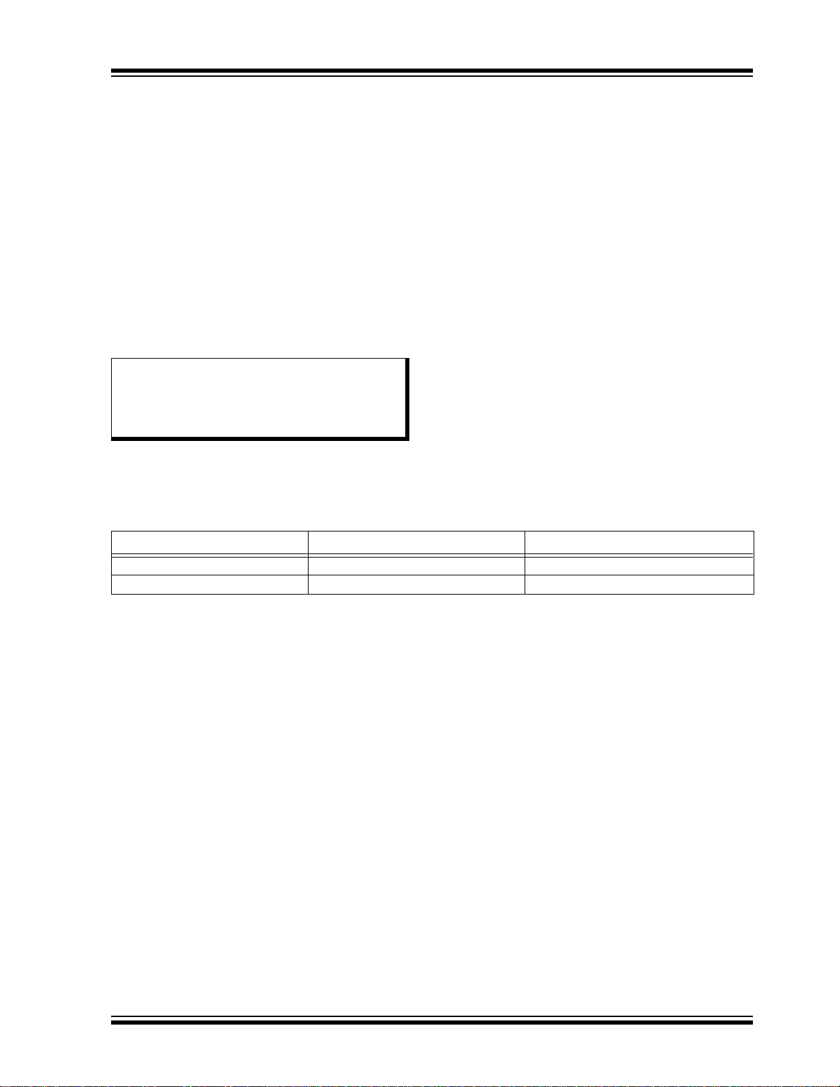
DS41414B-page 20 Preliminary 2010 Microchip Technology Inc.
PIC16F/LF1946/47
3.0 MEMORY ORGANIZATION
There are three types of memory in PIC16F/LF1946/47
devices: Data Memory, Program Memory and Data
EEPROM Memory
• Program Memory
• Data Memory
- Core Registers
- Special Function Registers
- General Purpose RAM
- Common RAM
- Device Memory Maps
- Special Function Registers Summary
• Data EEPROM memory
Note 1: The data EEPROM memory and the
(1)
.
(1)
method to access Flash memory through
the EECON registers is described in
Section 11.0 “Data EEPROM and Flash
Program Memory Control”.
The following features are associated with access and
control of program memory and data memory:
• PCL and PCLATH
•Stack
• Indirect Addressing
3.1 Program Memory Organization
The enhanced mid-range core has a 15-bit program
counter capable of addressing 32K x 14 program
memory space. Table 3-1 shows the memory sizes
implemented for the PIC16F/LF1946/47 family.
Accessing a location above these boundaries will cause
a wrap-around within the implemented memory space.
The Reset vector is at 0000h and the interrupt vector is
at 0004h (see Figures 3-1 and 3-2).
TABLE 3-1: DEVICE SIZES AND ADDRESSES
Device Program Memory Space (Words) Last Program Memory Address
PIC16F/LF1946 8,192 1FFFh
PIC16F/LF1947 16,384 3FFFh
2010 Microchip Technology Inc. Preliminary DS41414B-page 21
PIC16F/LF1946/47
PC<14:0>
15
0000h
0004h
Stack Level 0
Stack Level 15
Reset Vector
Interrupt Vector
Stack Level 1
0005h
On-chip
Program
Memory
Page 0
07FFh
Rollover to Page 0
0800h
0FFFh
1000h
7FFFh
Page 1
Rollover to Page 3
Page 2
Page 3
17FFh
1800h
1FFFh
2000h
CALL, CALLW
RETURN, RETLW
Interrupt, RETFIE
PC<14:0>
15
0000h
0004h
Stack Level 0
Stack Level 15
Reset Vector
Interrupt Vector
Stack Level 1
0005h
On-chip
Program
Memory
Page 0
07FFh
Rollover to Page 0
0800h
0FFFh
1000h
7FFFh
Page 1
Rollover to Page 7
Page 2
Page 3
17FFh
1800h
1FFFh
2000h
Page 4
Page 7
3FFFh
4000h
CALL, CALLW
RETURN, RETLW
Interrupt, RETFIE
FIGURE 3-1: PROGRAM MEMORY MAP
AND STACK FOR
PIC16F/LF1946
FIGURE 3-2: PROGRAM MEMORY MAP
AND STACK FOR
PIC16F/LF1947
DS41414B-page 22 Preliminary 2010 Microchip Technology Inc.

3.1.1 READING PROGRAM MEMORY AS
constants
BRW ;Add Index in W to
;program counter to
;select data
RETLW DATA0 ;Index0 data
RETLW DATA1 ;Index1 data
RETLW DATA2
RETLW DATA3
my_function
;… LOTS OF CODE…
MOVLW DATA_INDEX
CALL constants
;… THE CONSTANT IS IN W
DATA
There are two methods of accessing constants in program memory. The first method is to use tables of
RETLW instructions. The second method is to set an
FSR to point to the program memory.
3.1.1.1 RETLW Instruction
The RETLW instruction can be used to provide access
to tables of constants. The recommended way to create
such a table is shown in Example 3-1.
EXAMPLE 3-1: RETLW INSTRUCTION
PIC16F/LF1946/47
The BRW instruction makes this type of table very
simple to implement. If your code must remain portable
with previous generations of microcontrollers, then the
BRW instruction is not available so the older table read
method must be used.
2010 Microchip Technology Inc. Preliminary DS41414B-page 23

PIC16F/LF1946/47
constants
RETLW DATA0 ;Index0 data
RETLW DATA1 ;Index1 data
RETLW DATA2
RETLW DATA3
my_function
;… LOTS OF CODE…
MOVLW LOW constants
MOVWF FSR1L
MOVLW HIGH constants
MOVWF FSR1H
MOVIW 0[FSR1]
;THE PROGRAM MEMORY IS IN W
3.1.1.2 Indirect Read with FSR
The program memory can be accessed as data by setting bit 7 of the FSRxH register and reading the matching INDFx register. The MOVIW instruction will place the
lower 8 bits of the addressed word in the W register.
Writes to the program memory cannot be performed via
the INDF registers. Instructions that access the program memory via the FSR require one extra instruction
cycle to complete. Example 3-2 demonstrates accessing the program memory via an FSR.
The HIGH directive will set bit<7> if a label points to a
location in program memory.
EXAMPLE 3-2: ACCESSING PROGRAM
MEMORY VIA FSR
3.2.1 CORE REGISTERS
The core registers contain the registers that directly
affect the basic operation of the PIC16F/LF1946/47.
These registers are listed below:
• INDF0
• INDF1
•PCL
•STATUS
•FSR0 Low
• FSR0 High
•FSR1 Low
• FSR1 High
• BSR
•WREG
•PCLATH
• INTCON
Note: The core registers are the first 12
addresses of every data memory bank.
3.2 Data Memory Organization
The data memory is partitioned in 32 memory banks
with 128 bytes in a bank. Each bank consists of
(Figure 3-3):
• 12 core registers
• 20 Special Function Registers (SFR)
• Up to 80 bytes of General Purpose RAM (GPR)
• 16 bytes of common RAM
The active bank is selected by writing the bank number
into the Bank Select Register (BSR). Unimplemented
memory will read as ‘0’. All data memory can be
accessed either directly (via instructions that use the
file registers) or indirectly via the two File Select
Registers (FSR). See Section 3.5 “Indirect
Addressing” for more information.
DS41414B-page 24 Preliminary 2010 Microchip Technology Inc.
PIC16F/LF1946/47
3.2.1.1 STATUS Register
The STATUS register, shown in Register 3-1, contains:
• the arithmetic status of the ALU
• the Reset status
The STATUS register can be the destination for any
instruction, like any other register. If the STATUS
register is the destination for an instruction that affects
the Z, DC or C bits, then the write to these three bits is
disabled. These bits are set or cleared according to the
device logic. Furthermore, the TO
writable. Therefore, the result of an instruction with the
STATUS register as destination may be different than
intended.
and PD bits are not
For example, CLRF STATUS will clear the upper three
bits and set the Z bit. This leaves the STATUS register
as ‘000u u1uu’ (where u = unchanged).
It is recommended, therefore, that only BCF, BSF,
SWAPF and MOVWF instructions are used to alter the
STATUS register, because these instructions do not
affect any Status bits. For other instructions not
affecting any Status bits (Refer to Section 29.0
“Instruction Set Summary”).
Note 1: The C and DC bits operate as Borrow
and Digit Borrow out bits, respectively, in
subtraction.
REGISTER 3-1: STATUS: STATUS REGISTER
U-0 U-0 U-0 R-1/q R-1/q R/W-0/u R/W-0/u R/W-0/u
— — —
bit 7 bit 0
Legend:
R = Readable bit W = Writable bit U = Unimplemented bit, read as ‘0’
u = Bit is unchanged x = Bit is unknown -n/n = Value at POR and BOR/Value at all other Resets
‘1’ = Bit is set ‘0’ = Bit is cleared q = Value depends on condition
TO
PD ZDC
(1)
(1)
C
bit 7-5 Unimplemented: Read as ‘0’
bit 4 TO
bit 3 PD
bit 2 Z: Zero bit
bit 1 DC: Digit Carry/Digit Borrow
bit 0 C: Carry/Borrow
Note 1: For Borrow, the polarity is reversed. A subtraction is executed by adding the two’s complement of the
second operand. For rotate (RRF, RLF) instructions, this bit is loaded with either the high-order or low-order
bit of the source register.
: Time-out bit
1 = After power-up, CLRWDT instruction or SLEEP instruction
0 = A WDT time-out occurred
: Power-down bit
1 = After power-up or by the CLRWDT instruction
0 = By execution of the SLEEP instruction
1 = The result of an arithmetic or logic operation is zero
0 = The result of an arithmetic or logic operation is not zero
bit (ADDWF, ADDLW,SUBLW,SUBWF instructions)
1 = A carry-out from the 4th low-order bit of the result occurred
0 = No carry-out from the 4th low-order bit of the result
(1)
bit
(ADDWF, ADDLW, SUBLW, SUBWF instructions)
1 = A carry-out from the Most Significant bit of the result occurred
0 = No carry-out from the Most Significant bit of the result occurred
(1)
(1)
2010 Microchip Technology Inc. Preliminary DS41414B-page 25
PIC16F/LF1946/47
0Bh
0Ch
1Fh
20h
6Fh
70h
7Fh
00h
Common RAM
(16 bytes)
General Purpose RAM
(80 bytes maximum)
Core Registers
(12 bytes)
Special Function Registers
(20 bytes maximum)
Memory Region
7-bit Bank Offset
3.2.2 SPECIAL FUNCTION REGISTER
The Special Function Registers are registers used by
the application to control the desired operation of
peripheral functions in the device. The registers associated with the operation of the peripherals are
described in the appropriate peripheral chapter of this
data sheet.
3.2.3 GENERAL PURPOSE RAM
There are up to 80 bytes of GPR in each data memory
bank.
3.2.3.1 Linear Access to GPR
The general purpose RAM can be accessed in a
non-banked method via the FSRs. This can simplify
access to large memory structures. See Section 3.5.2
“Linear Data Memory” for more information.
3.2.4 COMMON RAM
There are 16 bytes of common RAM accessible from all
banks.
FIGURE 3-3: BANKED MEMORY
PARTITIONING
3.2.5 DEVICE MEMORY MAPS
The memory maps for the device family are as shown
in Table 3-2.
TABLE 3-2: MEMORY MAP TABLES
Device Banks Table No.
PIC16F/LF1946/47 0-7 Table 3-3
8-15 Table 3-4, Table 3-7
16-23 Table 3-5
23-31 Table 3-6, Table 3-8
DS41414B-page 26 Preliminary 2010 Microchip Technology Inc.
DS41414B-page 27 Preliminary 2010 Microchip Technology Inc.
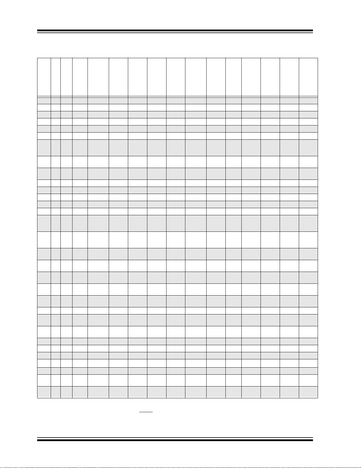
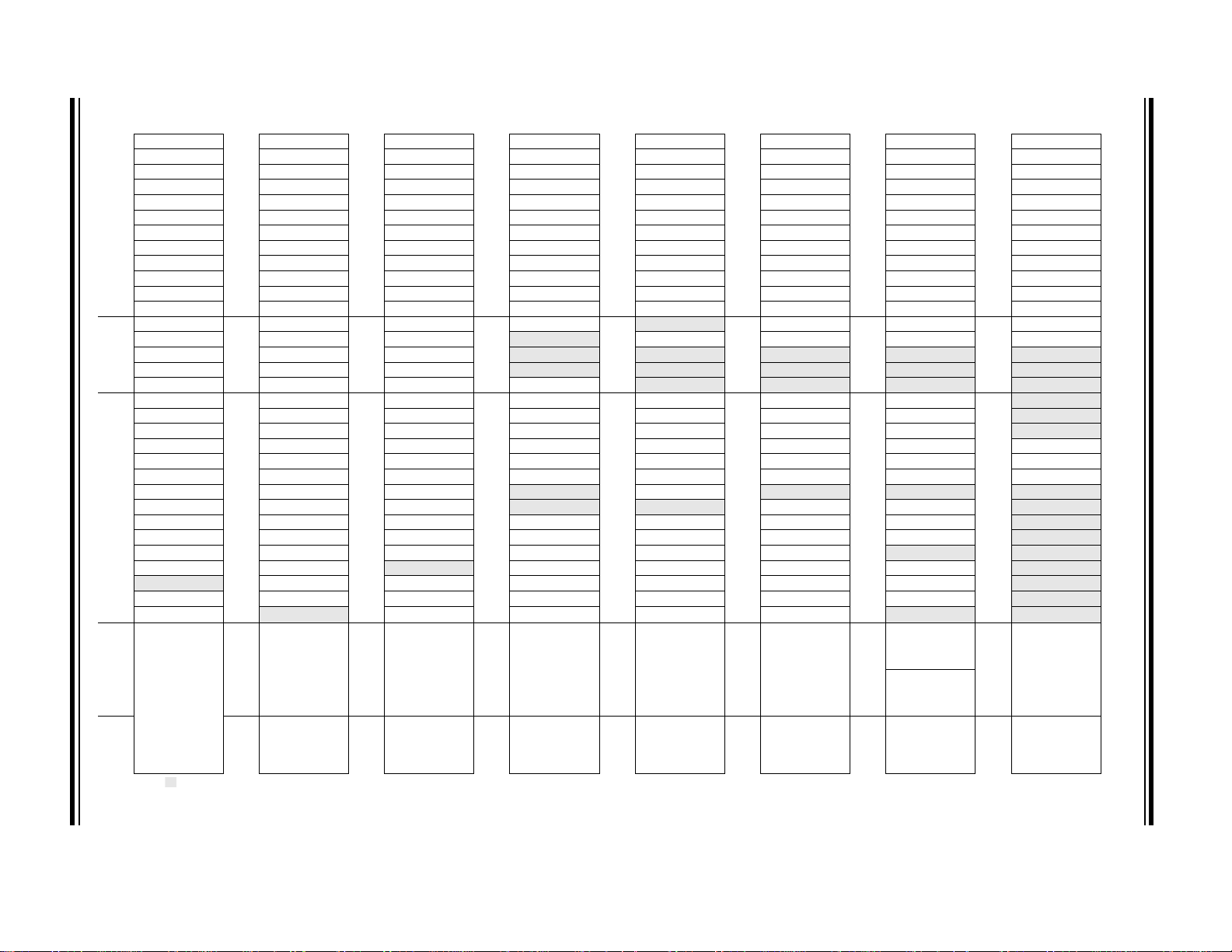
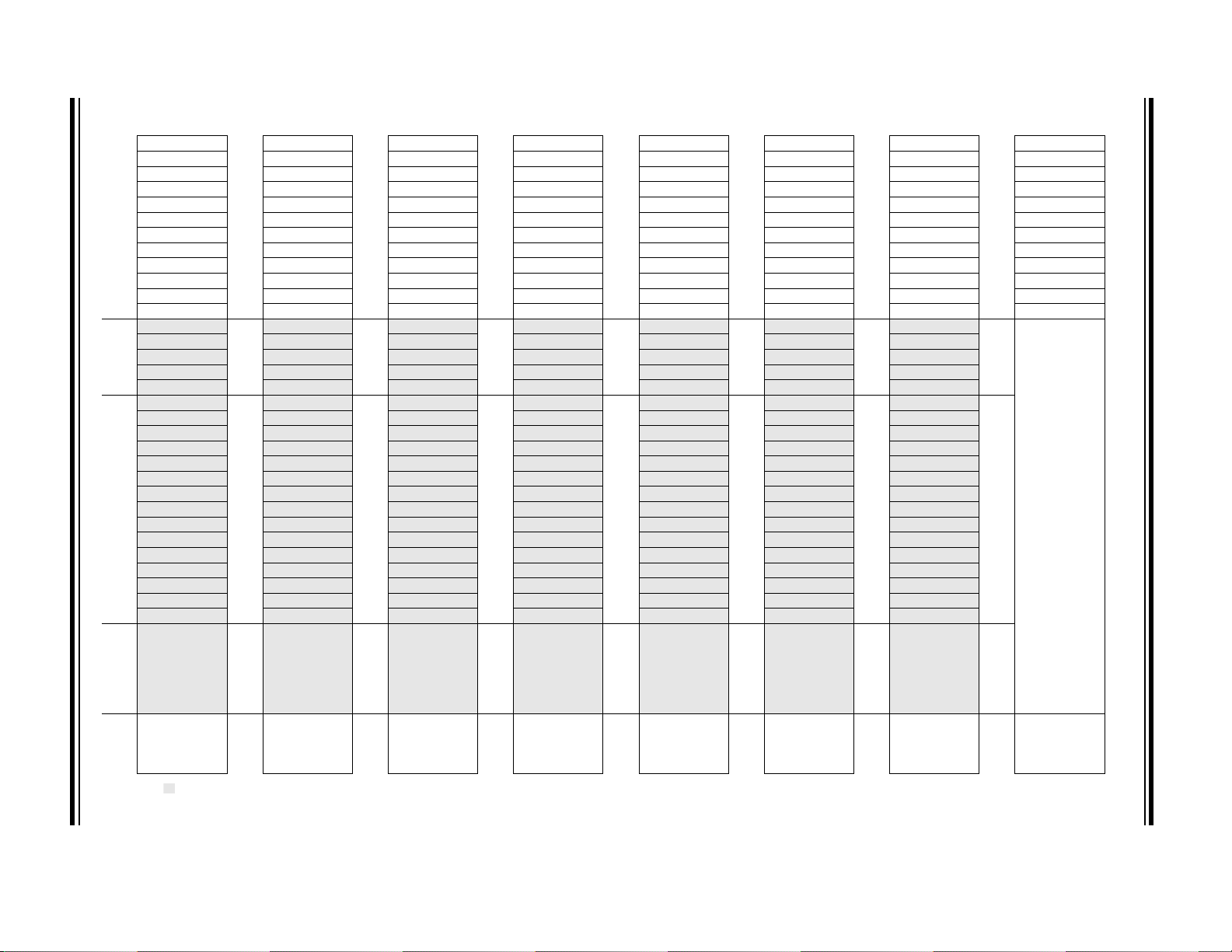
TABLE 3-3: PIC16F/LF1946/1947 MEMORY MAP, BANKS 0-7
PIC16F/LF1946/47
BANK 0 BANK 1 BANK 2 BANK 3 BANK 4 BANK 5 BANK 6 BANK 7
000h INDF0 080h INDF0 100h INDF0 180h INDF0 200h INDF0 280h INDF0 300h INDF0 380h INDF0
001h INDF1 081h INDF1 101h INDF1 181h INDF1 201h INDF1 281h INDF1 301h INDF1 381h INDF1
002h PCL 082h PCL 102h PCL 182h PCL 202h PCL 282h PCL 302h PCL 382h PCL
003h STATUS 083h STATUS 103h STATUS 183h STATUS 203h STATUS 283h STATUS 303h STATUS 383h STATUS
004h FSR0L 084h FSR0L 104h FSR0L 184h FSR0L 204h FSR0L 284h FSR0L 304h FSR0L 384h FSR0L
005h FSR0H 085h FSR0H 105h FSR0H 185h FSR0H 205h FSR0H 285h FSR0H 305h FSR0H 385h FSR0H
006h FSR1L 086h FSR1L 106h FSR1L 186h FSR1L 206h FSR1L 286h FSR1L 306h FSR1L 386h FSR1L
007h FSR1H 087h FSR1H 107h FSR1H 187h FSR1H 207h FSR1H 287h FSR1H 307h FSR1H 387h FSR1H
008h BSR 088h BSR 108h BSR 188h BSR 208h BSR 288h BSR 308h BSR 388h BSR
009h WREG 089h WREG 109h WREG 189h WREG 209h WREG 289h WREG 309h WREG 389h WREG
00Ah PCLATH 08Ah PCLATH 10Ah PCLATH 18Ah PCLATH 20Ah PCLATH 28Ah PCLATH 30Ah PCLATH 38Ah PCLATH
00Bh INTCON 08Bh INTCON 10Bh INTCON 18Bh INTCON 20Bh INTCON 28Bh INTCON 30Bh INTCON 38Bh INTCON
00Ch PORTA 08Ch TRISA 10Ch LATA 18Ch ANSELA 20Ch
00Dh PORTB 08Dh TRISB 10Dh LATB 18Dh
00Eh PORTC 08Eh TRISC 10Eh LATC 18Eh
00Fh PORTD 08Fh TRISD 10Fh LATD 18Fh
010h PORTE 090h TRISE 110h LATE 190h ANSELE 210h
011h PIR1 091h PIE1 111h CM1CON0 191h EEADRL 211h SSP1BUF 291h CCPR1L 311h CCPR3L 391h
012h PIR2 092h PIE2 112h CM1CON1 192h EEADRH 212h SSP1ADD 292h CCPR1H 312h CCPR3H 392h
013h PIR3 093h PIE3 113h CM2CON0 193h EEDATL 213h SSP1MSK 293h CCP1CON 313h CCP3CON 393h
014h PIR4 094h PIE4 114h CM2CON1 194h EEDATH 214h SSP1STAT 294h PWM1CON 314h PWM3CON 394h IOCBP
015h TMR0 095h OPTION 115h CMOUT 195h EECON1 215h SSP1CON1 295h CCP1AS 315h CCP3AS 395h IOCBN
016h TMR1L 096h PCON 116h BORCON 196h EECON2 216h SSP1CON2 296h PSTR1CON 316h PSTR3CON 396h IOCBF
017h TMR1H 097h WDTCON 117h FVRCON 197h
018h T1CON 098h OSCTUNE 118h DACCON0 198h
019h T1GCON 099h OSCCON 119h DACCON1 199h RC1REG 219h SSP2BUF 299h CCPR2H 319h CCPR4H 399h
01Ah TMR2 09Ah OSCSTAT 11Ah SRCON0 19Ah TX1REG 21Ah SSP2ADD 29Ah CCP2CON 31Ah CCP4CON 39Ah
01Bh PR2 09Bh ADRESL 11Bh SRCON1 19Bh SP1BRGL 21Bh SSP2MSK 29Bh PWM2CON 31Bh
01Ch T2CON 09Ch ADRESH 11Ch
01Dh
01Eh CPSCON0 09Eh ADCON1 11Eh CM3CON0 19Eh TX1STA 21Eh SSP2CON2 29Eh CCPTMRS0 31Eh CCP5CON 39Eh
01Fh CPSCON1 09Fh
020h
06Fh 0EFh 16Fh 1EFh 26Fh 2EFh
070h 0F0h
07Fh 0FFh 17Fh 1FFh 27Fh 2FFh 37Fh 3FFh
Legend: = Unimplemented data memory locations, read as ‘0’.
Note 1: Not available on PIC16F1946.
— 09Dh ADCON0 11Dh APFCON 19Dh RC1STA 21Dh SSP2CON1 29Dh PSTR2CON 31Dh CCPR5H 39Dh —
— 11Fh CM3CON1 19Fh BAUD1CON 21Fh SSP2CON3 29Fh CCPTMRS1 31Fh —39Fh—
General
Purpose
Register
80 Bytes
Accesses
70h – 7Fh
120h
170h
General
Purpose
Register
96 Bytes
0A0h
— 19Ch SP1BRGH 21Ch SSP2STAT 29Ch CCP2AS 31Ch CCPR5L 39Ch —
1A0h
General
Purpose
Register
80 Bytes
Accesses
70h – 7Fh
1F0h
— 20Dh WPUB 28Dh PORTG 30Dh TRISG 38Dh LATG
—20Eh—28Eh—30Eh—38Eh—
—20Fh—28Fh—30Fh—38Fh—
— 217h SSP1CON3 297h — 317h — 397h —
—218h— 298h CCPR2L 318h CCPR4L 398h —
220h
General
Purpose
Register
80 Bytes
Accesses
70h – 7Fh
270h
— 28Ch PORTF 30Ch TRISF 38Ch LATF
—290h— 310h — 390h —
—39Bh—
General
Purpose
Register
80 Bytes
Accesses
70h – 7Fh
2A0h
2F0h
General
Purpose
Register
80 Bytes
Accesses
70h – 7Fh
320h
General Purpose
Register
32Fh
330h
36Fh 3EFh
370h
16 Bytes
General Purpose
Register
64 Bytes
Accesses
70h – 7Fh
3A0h
(1)
3F0h
—
—
—
—
—
—
General
Purpose
Register
80 Bytes
Accesses
70h – 7Fh
(1)
DS41414B-page 28 Preliminary 2010 Microchip Technology Inc.
Legend: = Unimplemented data memory locations, read as ‘0’
Note 1: Not available on PIC16F1946.
BANK 8 BANK 9 BANK 10 BANK 11 BANK 12 BANK 13 BANK 14 BANK 15
400h
INDF0
480h
INDF0
500h
INDF0
580h
INDF0
600h
INDF0
680h
INDF0
700h
INDF0
780h
INDF0
401h
INDF1
481h
INDF1
501h
INDF1
581h
INDF1
601h
INDF1
681h
INDF1
701h
INDF1
781h
INDF1
402h
PCL
482h
PCL
502h
PCL
582h
PCL
602h
PCL
682h
PCL
702h
PCL
782h
PCL
403h
STATUS
483h
STATUS
503h
STATUS
583h
STATUS
603h
STATUS
683h
STATUS
703h
STATUS
783h
STATUS
404h
FSR0L
484h
FSR0L
504h
FSR0L
584h
FSR0L
604h
FSR0L
684h
FSR0L
704h
FSR0L
784h
FSR0L
405h
FSR0H
485h
FSR0H
505h
FSR0H
585h
FSR0H
605h
FSR0H
685h
FSR0H
705h
FSR0H
785h
FSR0H
406h
FSR1L
486h
FSR1L
506h
FSR1L
586h
FSR1L
606h
FSR1L
686h
FSR1L
706h
FSR1L
786h
FSR1L
407h
FSR1H
487h
FSR1H
507h
FSR1H
587h
FSR1H
607h
FSR1H
687h
FSR1H
707h
FSR1H
787h
FSR1H
408h
BSR
488h
BSR
508h
BSR
588h
BSR
608h
BSR
688h
BSR
708h
BSR
788h
BSR
409h
WREG
489h
WREG
509h
WREG
589h
WREG
609h
WREG
689h
WREG
709h
WREG
789h
WREG
40Ah
PCLATH
48Ah
PCLATH
50Ah
PCLATH
58Ah
PCLATH
60Ah
PCLATH
68Ah
PCLATH
70Ah
PCLATH
78Ah
PCLATH
40Bh
INTCON
48Bh
INTCON
50Bh
INTCON
58Bh
INTCON
60Bh
INTCON
68Bh
INTCON
70Bh
INTCON
78Bh
INTCON
40Ch
ANSELF
48Ch
—
50Ch
—
58Ch
—
60Ch
—
68Ch
—
70Ch
—
78Ch
—
40Dh
ANSELG
48Dh
WPUG
50Dh
—
58Dh
—
60Dh
—
68Dh
—
70Dh
—
78Dh
—
40Eh
—
48Eh
—
50Eh
—
58Eh
—
60Eh
—
68Eh
—
70Eh
—
78Eh
—
40Fh
—
48Fh
—
50Fh
—
58Fh
—
60Fh
—
68Fh
—
70Fh
—
78Fh
—
410h
—
490h
—
510h
—
590h
—
610h
—
690h
—
710h
—
790h
—
411h
—
491h
RC2REG
511h
—
591h
—
611h
—
691h
—
711h
—
791h
See Ta bl e 3 -7
412h
—
492h
TX2REG
512h
—
592h
—
612h
—
692h
—
712h
—
792h
413h
—
493h
SP2BRG
513h
—
593h
—
613h
—
693h
—
713h
—
793h
414h
—
494h
SP2BRGH
514h
—
594h
—
614h
—
694h
—
714h
—
794h
415h
TMR4
495h
RC2STA
515h
—
595h
—
615h
—
695h
—
715h
—
795h
416h
PR4
496h
TX2STA
516h
—
596h
—
616h
—
696h
—
716h
—
796h
417h
T4CON
497h
BAUDCON2
517h
—
597h
—
617h
—
697h
—
717h
—
797h
418h
—
498h
—
518h
—
598h
—
618h
—
698h
—
718h
—
798h
419h
—
499h
—
519h
—
599h
—
619h
—
699h
—
719h
—
799h
41Ah
—
49Ah
—
51Ah
—
59Ah
—
61Ah
—
69Ah
—
71Ah
—
79Ah
41Bh
—
49Bh
—
51Bh
—
59Bh
—
61Bh
—
69Bh
—
71Bh
—
79Bh
41Ch
TMR6
49Ch
—
51Ch
—
59Ch
—
61Ch
—
69Ch
—
71Ch
—
79Ch
41Dh
PR6
49Dh
—
51Dh
—
59Dh
—
61Dh
—
69Dh
—
71Dh
—
79Dh
41Eh
T6CON
49Eh
—
51Eh
—
59Eh
—
61Eh
—
69Eh
—
71Eh
—
79Eh
41Fh
—
49Fh
—
51Fh
—
59Fh
—
61Fh
—
69Fh
—
71Fh
—
79Fh
420h
General
Purpose
Register
80 Bytes
(1)
4A0h
General
Purpose
Register
80 Bytes
(1)
520h
General
Purpose
Register
80 Bytes
(1)
5A0h
General
Purpose
Register
80 Bytes
(1)
620h
General Purpose
Register
48 Bytes
(1)
6A0h
Unimplemented
Read as ‘0’
720h
Unimplemented
Read as ‘0’
7A0h
Unimplemented
Read as ‘0’
46Fh 4EFh 56Fh 5EFh 66Fh 6EFh 76Fh 7EFh
470h
Accesses
70h – 7Fh
4F0h
Accesses
70h – 7Fh
570h
Accesses
70h – 7Fh
5F0h
Accesses
70h – 7Fh
670h
Accesses
70h – 7Fh
6F0h
Accesses
70h – 7Fh
770h
Accesses
70h – 7Fh
7F0h
Accesses
70h – 7Fh
47Fh
4FFh 57Fh
5FFh 67Fh 6FFh 77Fh 7FFh
TABLE 3-4: PIC16F/LF1946/1947 MEMORY MAP, BANKS 8-15
PIC16F/LF1946/47
DS41414B-page 29 Preliminary 2010 Microchip Technology Inc.
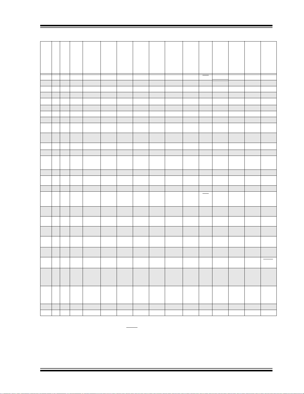
TABLE 3-5: PIC16F/LF1946/47 MEMORY MAP, BANKS 16-23
PIC16F/LF1946/47
BANK 16 BANK 17 BANK 18 BANK 19 BANK 20 BANK 21 BANK 22 BANK 23
800h INDF0 880h INDF0 900h INDF0 980h INDF0 A00h INDF0 A80h INDF0 B00h INDF0 B80h INDF0
801h INDF1 881h INDF1 901h INDF1 981h INDF1 A01h INDF1 A81h INDF1 B01h INDF1 B81h INDF1
802h PCL 882h PCL 902h PCL 982h PCL A02h PCL A82h PCL B02h PCL B82h PCL
803h STATUS 883h STATUS 903h STATUS 983h STATUS A03h STATUS A83h STATUS B03h STATUS B83h STATUS
804h FSR0L 884h FSR0L 904h FSR0L 984h FSR0L A04h FSR0L A84h FSR0L B04h FSR0L B84h FSR0L
805h FSR0H 885h FSR0H 905h FSR0H 985h FSR0H A05h FSR0H A85h FSR0H B05h FSR0H B85h FSR0H
806h FSR1L 886h FSR1L 906h FSR1L 986h FSR1L A06h FSR1L A86h FSR1L B06h FSR1L B86h FSR1L
807h FSR1H 887h FSR1H 907h FSR1H 987h FSR1H A07h FSR1H A87h FSR1H B07h FSR1H B87h FSR1H
808h BSR 888h BSR 908h BSR 988h BSR A08h BSR A88h BSR B08h BSR B88h BSR
809h WREG 889h WREG 909h WREG 989h WREG A09h WREG A89h WREG B09h WREG B89h WREG
80Ah PCLATH 88Ah PCLATH 90Ah PCLATH 98Ah PCLATH A0Ah PCLATH A8Ah PCLATH B0Ah PCLATH B8Ah PCLATH
80Bh INTCON 88Bh INTCON 90Bh INTCON 98Bh INTCON A0Bh INTCON A8Bh INTCON B0Bh INTCON B8Bh INTCON
80Ch
80Dh
80Eh
80Fh
810h
811h
812h
813h
814h
815h
816h
817h
818h
819h
81Ah
81Bh
81Ch
81Dh
81Eh
81Fh
820h
— 88Ch — 90Ch — 98Ch —A0Ch—A8Ch—B0Ch—B8Ch—
— 88Dh — 90Dh — 98Dh —A0Dh—A8Dh—B0Dh—B8Dh—
—88Eh—90Eh—98Eh—A0Eh—A8Eh—B0Eh—B8Eh—
—88Fh—90Fh—98Fh—A0Fh—A8Fh—B0Fh—B8Fh—
—890h—910h—990h—A10h—A90h—B10h—B90h—
—891h—911h—991h—A11h—A91h—B11h—B91h—
—892h—912h—992h—A12h—A92h—B12h—B92h—
—893h—913h—993h—A13h—A93h—B13h—B93h—
—894h—914h—994h—A14h—A94h—B14h—B94h—
—895h—915h—995h—A15h—A95h—B15h—B95h—
—896h—916h—996h—A16h—A96h—B16h—B96h—
—897h—917h—997h—A17h—A97h—B17h—B97h—
—898h—918h—998h—A18h—A98h—B18h—B98h—
—899h—919h—999h—A19h—A99h—B19h—B99h—
—89Ah—91Ah—99Ah—A1Ah—A9Ah—B1Ah—B9Ah—
—89Bh—91Bh—99Bh—A1Bh—A9Bh—B1Bh—B9Bh—
— 89Ch — 91Ch — 99Ch —A1Ch—A9Ch—B1Ch—B9Ch—
— 89Dh — 91Dh — 99Dh —A1Dh—A9Dh—B1Dh—B9Dh—
—89Eh—91Eh—99Eh—A1Eh—A9Eh—B1Eh—B9Eh—
—89Fh—91Fh—99Fh—A1Fh—A9Fh—B1Fh—B9Fh—
8A0h
920h
9A0h
A20h
AA0h
B20h
BA0h
Unimplemented
Read as ‘0’
86Fh 8EFh 96Fh
870h
87Fh 8FFh 97Fh 9FFh A7Fh AFFh B7Fh BFFh
Legend: = Unimplemented data memory locations, read as ‘0’.
Accesses
70h – 7Fh
8F0h
Unimplemented
Read as ‘0’
Accesses
70h – 7Fh
970h
Unimplemented
Read as ‘0’
Accesses
70h – 7Fh
9EFh
9F0h
Unimplemented
Read as ‘0’
Accesses
70h – 7Fh
A6Fh
A70h
Unimplemented
Read as ‘0’
Accesses
70h – 7Fh
AEFh
AF0h
Unimplemented
Read as ‘0’
Accesses
70h – 7Fh
B6Fh
B70h
Unimplemented
Read as ‘0’
Accesses
70h – 7Fh
BEFh
BF0h
Unimplemented
Read as ‘0’
Accesses
70h – 7Fh
DS41414B-page 30 Preliminary 2010 Microchip Technology Inc.
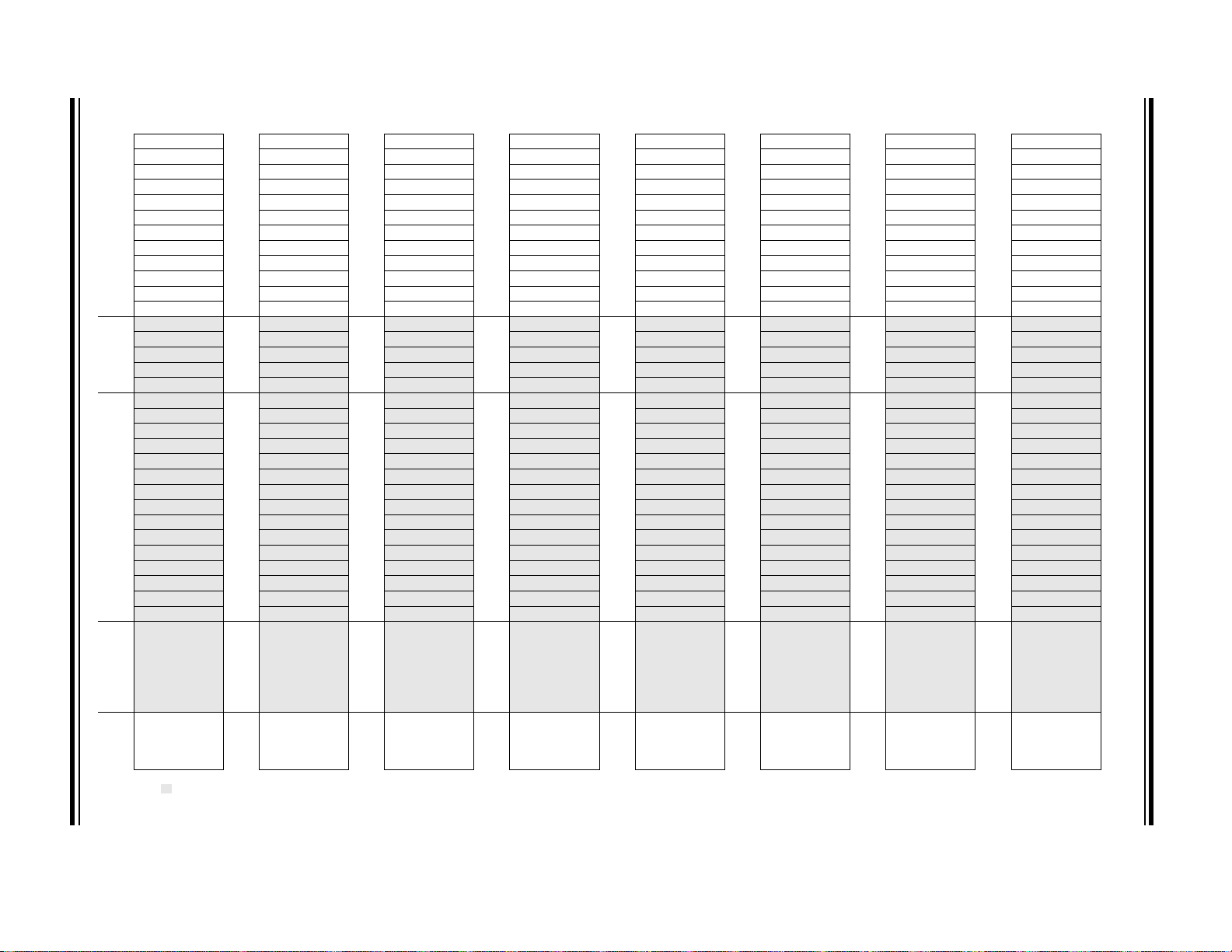
Legend: = Unimplemented data memory locations, read as ‘0’.
BANK 24 BANK 25 BANK 26 BANK 27 BANK 28 BANK 29 BANK 30 BANK 31
C00h INDF0 C80h INDF0 D00h INDF0 D80h INDF0 E00h INDF0 E80h INDF0 F00h INDF0 F80h INDF0
C01h INDF1 C81h INDF1 D01h INDF1 D81h INDF1 E01h INDF1 E81h INDF1 F01h INDF1 F81h INDF1
C02h PCL C82h PCL D02h PCL D82h PCL E02h PCL E82h PCL F02h PCL F82h PCL
C03h STATUS C83h STATUS D03h STATUS D83h STATUS E03h STATUS E83h STATUS F03h STATUS F83h STATUS
C04h FSR0L C84h FSR0L D04h FSR0L D84h FSR0L E04h FSR0L E84h FSR0L F04h FSR0L F84h FSR0L
C05h FSR0H C85h FSR0H D05h FSR0H D85h FSR0H E05h FSR0H E85h FSR0H F05h FSR0H F85h FSR0H
C06h FSR1L C86h FSR1L D06h FSR1L D86h FSR1L E06h FSR1L E86h FSR1L F06h FSR1L F86h FSR1L
C07h FSR1H C87h FSR1H D07h FSR1H D87h FSR1H E07h FSR1H E87h FSR1H F07h FSR1H F87h FSR1H
C08h BSR C88h BSR D08h BSR D88h BSR E08h BSR E88h BSR F08h BSR F88h BSR
C09h WREG C89h WREG D09h WREG D89h WREG E09h WREG E89h WREG F09h WREG F89h WREG
C0Ah PCLATH C8Ah PCLATH D0Ah PCLATH D8Ah PCLATH E0Ah PCLATH E8Ah PCLATH F0Ah PCLATH F8Ah PCLATH
C0Bh INTCON C8Bh INTCON D0Bh INTCON D8Bh INTCON E0Bh INTCON E8Bh INTCON F0Bh INTCON F8Bh INTCON
C0Ch
—C8Ch—D0Ch—D8Ch—E0Ch—E8Ch—F0Ch—F8Ch
See Ta bl e 3 -8
C0Dh
—C8Dh—D0Dh—D8Dh—E0Dh—E8Dh—F0Dh—F8Dh
C0Eh
—C8Eh—D0Eh—D8Eh—E0Eh—E8Eh—F0Eh—F8Eh
C0Fh
—C8Fh—D0Fh—D8Fh—E0Fh—E8Fh—F0Fh—F8Fh
C10h
—C90h—D10h—D90h—E10h—E90h—F10h—F90h
C11h
—C91h—D11h—D91h—E11h—E91h—F11h—F91h
C12h
—C92h—D12h—D92h—E12h—E92h—F12h—F92h
C13h
—C93h—D13h—D93h—E13h—E93h—F13h—F93h
C14h
—C94h—D14h—D94h—E14h—E94h—F14h—F94h
C15h
—C95h—D15h—D95h—E15h—E95h—F15h—F95h
C16h
—C96h—D16h—D96h—E16h—E96h—F16h—F96h
C17h
—C97h—D17h—D97h—E17h—E97h—F17h—F97h
C18h
—C98h—D18h—D98h—E18h—E98h—F18h—F98h
C19h
—C99h—D19h—D99h—E19h—E99h—F19h—F99h
C1Ah
—C9Ah—D1Ah—D9Ah—E1Ah—E9Ah—F1Ah—F9Ah
C1Bh
—C9Bh—D1Bh—D9Bh—E1Bh—E9Bh—F1Bh—F9Bh
C1Ch
—C9Ch—D1Ch—D9Ch—E1Ch—E9Ch—F1Ch—F9Ch
C1Dh
—C9Dh—D1Dh—D9Dh—E1Dh—E9Dh—F1Dh—F9Dh
C1Eh
—C9Eh—D1Eh—D9Eh—E1Eh—E9Eh—F1Eh—F9Eh
C1Fh
—C9Fh—D1Fh—D9Fh—E1Fh—E9Fh—F1Fh—F9Fh
C20h
Unimplemented
Read as ‘0’
CA0h
Unimplemented
Read as ‘0’
D20h
Unimplemented
Read as ‘0’
DA0h
Unimplemented
Read as ‘0’
E20h
Unimplemented
Read as ‘0’
EA0h
Unimplemented
Read as ‘0’
F20h
Unimplemented
Read as ‘0’
FA0h
C6Fh CEFh D6Fh DEFh E6Fh EEFh F6Fh FEFh
C70h
Accesses
70h – 7Fh
CF0h
Accesses
70h – 7Fh
D70h
Accesses
70h – 7Fh
DF0h
Accesses
70h – 7Fh
E70h
Accesses
70h – 7Fh
EF0h
Accesses
70h – 7Fh
F70h
Accesses
70h – 7Fh
FF0h
Accesses
70h – 7Fh
CFFh
CFFh D7Fh DFFh E7Fh EFFh F7Fh FFFh
TABLE 3-6: PIC16F/LF1946/47 MEMORY MAP, BANKS 24-31
PIC16F/LF1946/47

PIC16F/LF1946/47
Legend: = Unimplemented data memory locations,
read as ‘0’.
Bank 15
791h
LCDCON
792h
LCDPS
793h
LCDREF
794h
LCDCST
795h
LCDRL
796h
—
797h
—
798h
LCDSE0
799h
LCDSE1
79Ah
LCDSE2
79Bh
LCDSE3
79Ch
LCDSE4
79Dh
LCDSE5
79Eh
—
79Fh
—
7A0h LCDDATA0
7A1h LCDDATA1
7A2h LCDDATA2
7A3h LCDDATA3
7A4h LCDDATA4
7A5h LCDDATA5
7A6h LCDDATA6
7A7h LCDDATA7
7A8h LCDDATA8
7A9h LCDDATA9
7AAh LCDDATA10
7ABh LCDDATA11
7ACh LCDDATA12
7ADh LCDDATA13
7AEh LCDDATA14
7AFh LCDDATA15
7B0h LCDDATA16
7B1h LCDDATA17
7B2h LCDDATA18
7B3h LCDDATA19
7B4h LCDDATA20
7B5h LCDDATA21
7B6h LCDDATA22
7B7h LCDDATA23
7B8h
Unimplemented
Read as ‘0’
7EFh
Legend: = Unimplemented data memory locations,
read as ‘0’.
Bank 31
F8Ch ICDIO
(2)
F8Dh ICDCON0
(2)
F8Eh ICDCON1
(2)
F8Fh ICDCON2
(2)
F90h
—
F91h ICDSTAT
(2)
F92h
—
F93h
—
F94h
—
F95h
DEVSEL
(2)
F96h ICDINSTL
(2)
F97h ICDINSTH
(2)
F98h ICDCC0
(2)
F99h ICDCC1
(2)
F9Ah
ICDCC2
(2)
F9Bh ICDCC3
(2)
F9Ch ICDBK0CON
(2)
F9Dh ICDBK0L
(2)
F9Eh ICDBK0H
(2)
F9Fh ICDBK0D
(2)
FA0h ICDBK0CNT
(2)
FA1h ICDBK1CON
(2)
FA2h ICDBK1L
(2)
FA3h ICDBK1H
(2)
FA4h ICDBK1D
(2)
FA5h ICDBK1CNT
(2)
FA6h ICDBK2CON
(2)
FA7h ICDBK2L
(2)
FA8h ICDBK2H
(2)
FA9h ICDBK2D
(2)
FAAh ICDBK2CNT
(2)
FABh
—
FDFh
FC0h
—
FDFh
FE0h
—
FE1h
—
FE2h
—
FE3h
BSR_ICDSHAD
(2)
FE4h
STATUS_SHAD
FE5h
WREG_SHAD
FE6h
BSR_SHAD
FE7h
PCLATH_SHAD
FE8h
FSR0L_SHAD
FE9h
FSR0H_SHAD
FEAh
FSR1L_SHAD
FEBh
FSR1H_SHAD
FECh
—
FEDh
STKPTR
FEEh
TOSL
FEFh
TOSH
TABLE 3-7: PIC16F/LF1946/47 MEMORY
MAP, BANK 15
2010 Microchip Technology Inc. Preliminary DS41414B-page 31
TABLE 3-8: PIC16F/LF1946/47 MEMORY
MAP, BANK 31

PIC16F/LF1946/47
3.2.6 SPECIAL FUNCTION REGISTERS SUMMARY
The Special Function Register Summary for the device
family are as follows:
Device Bank(s) Page No.
033
134
235
336
437
538
PIC16F/LF1946/47
639
740
841
9-14 43
15 44
16-30 46
31 47
DS41414B-page 32 Preliminary 2010 Microchip Technology Inc.

PIC16F/LF1946/47
TABLE 3-9: SPECIAL FUNCTION REGISTER SUMMARY
Address Name Bit 7 Bit 6 Bit 5 Bit 4 Bit 3 Bit 2 Bit 1 Bit 0
Bank 0
(2)
000h
001h
002h
003h
004h
005h
006h
007h
008h
009h
00Ah
00Bh
00Ch PORTA PORTA Data Latch when written: PORTA pins when read xxxx xxxx uuuu uuuu
00Dh PORTB PORTB Data Latch when written: PORTB pins when read xxxx xxxx uuuu uuuu
00Eh PORTC PORTC Data Latch when written: PORTC pins when read xxxx xxxx uuuu uuuu
00Fh PORTD PORTD Data Latch when written: PORTD pins when read xxxx xxxx uuuu uuuu
010h PORTE PORTE Data Latch when written: PORTE pins when read xxxx xxxx xxxx uuuu
011h PIR1 TMR1GIF ADIF RCIF TXIF SSPIF CCP1IF TMR2IF TMR1IF 0000 0000 0000 0000
012h PIR2 OSFIF C2IF C1IF EEIF BCLIF LCDIF C3IF CCP2IF 0000 0000 0000 0000
013h PIR3
014h PIR4
015h TMR0 Timer0 Module Register xxxx xxxx uuuu uuuu
016h TMR1L Holding Register for the Least Significant Byte of the 16-bit TMR1 Register xxxx xxxx uuuu uuuu
017h TMR1H Holding Register for the Most Significant Byte of the 16-bit TMR1 Register xxxx xxxx uuuu uuuu
018h T1CON TMR1CS<1:0> T1CKPS<1:0> T1OSCEN T1SYNC
019h T1GCON TMR1GE T1GPOL T1GTM T1GSPM T1GGO/
01Ah TMR2 Timer 2 Module Register 0000 0000 0000 0000
01Bh PR2 Timer 2 Period Register 1111 1111 1111 1111
01Ch T2CON
01Dh
01Eh CPSCON0 CPSON CPSRM
01Fh CPSCON1
Legend: x = unknown, u = unchanged, q = value depends on condition, - = unimplemented, read as ‘0’, r = reserved.
Note 1: The upper byte of the program counter is not directly accessible. PCLATH is a holding register for the PC<14:8>, whose contents are transferred
INDF0 Addressing this location uses contents of FSR0H/FSR0L to address data memory
(2)
INDF1 Addressing this location uses contents of FSR1H/FSR1L to address data memory
(2)
PCL Program Counter (PC) Least Significant Byte 0000 0000 0000 0000
(2)
STATUS — — —TOPD ZDCC---1 1000 ---q quuu
(2)
FSR0L Indirect Data Memory Address 0 Low Pointer 0000 0000 uuuu uuuu
(2)
FSR0H Indirect Data Memory Address 0 High Pointer 0000 0000 0000 0000
(2)
FSR1L Indirect Data Memory Address 1 Low Pointer 0000 0000 uuuu uuuu
(2)
FSR1H Indirect Data Memory Address 1 High Pointer 0000 0000 0000 0000
(2)
BSR — — — BSR<4:0> ---0 0000 ---0 0000
(2)
WREG Working Register 0000 0000 uuuu uuuu
(1, 2)
PCLATH — Write Buffer for the upper 7 bits of the Program Counter -000 0000 -000 0000
(2)
INTCON GIE PEIE TMR0IE INTE IOCIE TMR0IF INTF IOCIF 0000 000x 0000 000u
— Unimplemented — —
Shaded locations are unimplemented, read as ‘0’.
to the upper byte of the program counter.
2: These registers can be addressed from any bank.
(not a physical register)
(not a physical register)
— CCP5IF CCP4IF CCP3IF TMR6IF —TMR4IF— -000 0-0- -000 0-0-
— — RC2IF TX2IF — — BCL2IF SSP2IF --00 --00 --00 --00
—TMR1ON0000 00-0 uuuu uu-u
T1GVAL T1GSS<1:0> 0000 0x00 uuuu uxuu
DONE
— T2OUTPS<3:0> TMR2ON T2CKPS<1:0> -000 0000 -000 0000
— — CPSRNG1 CPSRNG0 CPSOUT T0XCS 00-- 0000 00-- 0000
— — — CPSCH<4:0> ---0 0000 ---0 0000
Value on:
POR, BOR
xxxx xxxx xxxx xxxx
xxxx xxxx xxxx xxxx
Value on all
other
Resets
2010 Microchip Technology Inc. Preliminary DS41414B-page 33
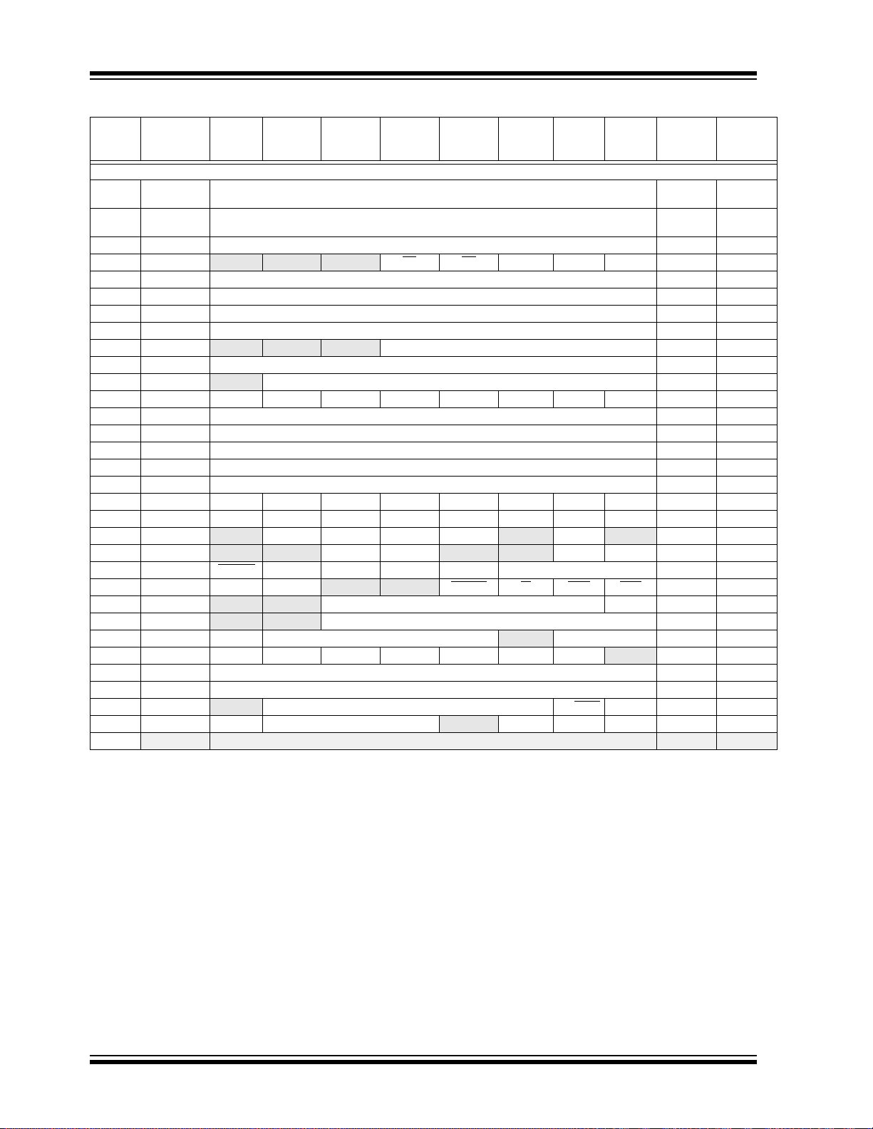
PIC16F/LF1946/47
TABLE 3-9: SPECIAL FUNCTION REGISTER SUMMARY (CONTINUED)
Address Name Bit 7 Bit 6 Bit 5 Bit 4 Bit 3 Bit 2 Bit 1 Bit 0
Bank 1
(2)
080h
081h
082h
083h
084h
085h
086h
087h
088h
089h
08Ah
08Bh
08Ch TRISA PORTA Data Direction Register 1111 1111 1111 1111
08Dh TRISB PORTB Data Direction Register 1111 1111 1111 1111
08Eh TRISC PORTC Data Direction Register 1111 1111 1111 1111
08Fh TRISD PORTD Data Direction Register 1111 1111 1111 1111
090h TRISE PORTE Data Direction Register 1111 1111 1111 1111
091h PIE1 TMR1GIE ADIE RCIE TXIE SSPIE CCP1IE TMR2IE TMR1IE 0000 0000 0000 0000
092h PIE2 OSFIE C2IE C1IE EEIE BCLIE LCDIE C3IE CCP2IE 0000 0000 0000 0000
093h PIE3
094h PIE4
095h OPTION_REG WPUEN
096h PCON STKOVF STKUNF
097h WDTCON
098h OSCTUNE
099h OSCCON SPLLEN IRCF<3:0>
09Ah OSCSTAT T1OSCR PLLR OSTS HFIOFR HFIOFL MFIOFR LFIOFR
09Bh ADRESL A/D Result Register Low xxxx xxxx uuuu uuuu
09Ch ADRESH A/D Result Register High xxxx xxxx uuuu uuuu
09Dh ADCON0
09Eh ADCON1 ADFM ADCS<2:0>
09Fh
Legend: x = unknown, u = unchanged, q = value depends on condition, - = unimplemented, read as ‘0’, r = reserved.
Note 1: The upper byte of the program counter is not directly accessible. PCLATH is a holding register for the PC<14:8>, whose contents are transferred
INDF0 Addressing this location uses contents of FSR0H/FSR0L to address data memory
(2)
INDF1 Addressing this location uses contents of FSR1H/FSR1L to address data memory
(2)
PCL Program Counter (PC) Least Significant Byte 0000 0000 0000 0000
(2)
STATUS — — —TOPD ZDCC---1 1000 ---q quuu
(2)
FSR0L Indirect Data Memory Address 0 Low Pointer 0000 0000 uuuu uuuu
(2)
FSR0H Indirect Data Memory Address 0 High Pointer 0000 0000 0000 0000
(2)
FSR1L Indirect Data Memory Address 1 Low Pointer 0000 0000 uuuu uuuu
(2)
FSR1H Indirect Data Memory Address 1 High Pointer 0000 0000 0000 0000
(2)
BSR — — — BSR<4:0> ---0 0000 ---0 0000
(2)
WREG Working Register 0000 0000 uuuu uuuu
(1, 2)
PCLATH — Write Buffer for the upper 7 bits of the Program Counter -000 0000 -000 0000
(2)
INTCON GIE PEIE TMR0IE INTE IOCIE TMR0IF INTF IOCIF 0000 000x 0000 000u
— Unimplemented — —
Shaded locations are unimplemented, read as ‘0’.
to the upper byte of the program counter.
2: These registers can be addressed from any bank.
(not a physical register)
(not a physical register)
— CCP5IE CCP4IE CCP3IE TMR6IE —TMR4IE— -000 0-0- -000 0-0-
— — RC2IE TX2IE — — BCL2IE SSP2IE --00 --00 --00 --00
INTEDG T0CS T0SE PSA PS<2:0> 1111 1111 1111 1111
— —RMCLRRI POR BOR 00-- 11qq qq-- qquu
— — WDTPS<4:0> SWDTEN --01 0110 --01 0110
— —TUN<5:0>--00 0000 --00 0000
—SCS<1:0>0011 1-00 0011 1-00
HFIOFS 00q0 0q0- qqqq qq0-
— CHS<4:0>
— ADNREF
GO/DONE
ADPREF1
ADON -000 0000 -000 0000
ADPREF0 0000 -000 0000 -000
Value on:
POR, BOR
xxxx xxxx xxxx xxxx
xxxx xxxx xxxx xxxx
Value on all
other
Resets
DS41414B-page 34 Preliminary 2010 Microchip Technology Inc.

PIC16F/LF1946/47
TABLE 3-9: SPECIAL FUNCTION REGISTER SUMMARY (CONTINUED)
Address Name Bit 7 Bit 6 Bit 5 Bit 4 Bit 3 Bit 2 Bit 1 Bit 0
Bank 2
(2)
100h
101h
102h
103h
104h
105h
106h
107h
108h
109h
10Ah
10Bh
10Ch LATA PORTA Data Latch xxxx xxxx uuuu uuuu
10Dh LATB PORTB Data Latch xxxx xxxx uuuu uuuu
10Eh LATC PORTC Data Latch xxxx xxxx uuuu uuuu
10Fh LATD PORTD Data Latch xxxx xxxx uuuu uuuu
110h LATE PORTE Data Latch xxxx xxxx uuuu uuuu
111h CM1CON0 C1ON C1OUT C1OE C1POL
112h CM1CON1 C1INTP C1INTN C1PCH1 C1PCH0
113h CM2CON0 C2ON C2OUT C2OE C2POL
114h CM2CON1 C2INTP C2INTN C2PCH1 C2PCH0
115h CMOUT
116h BORCON SBOREN
117h FVRCON FVREN FVRRDY TSEN TSRNG CDAFVR1 CDAFVR0 ADFVR<1:0> 0q00 0000 0q00 0000
118h DACCON0 DACEN DACLPS DACOE
119h DACCON1
11Ah SRCON0 SRLEN SRCLK2 SRCLK1 SRCLK0 SRQEN SRNQEN SRPS SRPR 0000 0000 0000 0000
11Bh SRCON1 SRSPE SRSCKE SRSC2E SRSC1E SRRPE SRRCKE SRRC2E SRRC1E 0000 0000 0000 0000
11Ch
11Dh APFCON P3CSEL P3BSEL P2DSEL P2CSEL P2BSEL CCP2SEL P1CSEL P1BSEL 0000 0000 0000 0000
11Eh CM3CON0 C3ON C3OUT C3OE C3POL
11Fh CM3CON1 C3INTP C3INTN C3PCH1 C3PCH0
Legend: x = unknown, u = unchanged, q = value depends on condition, - = unimplemented, read as ‘0’, r = reserved.
Note 1: The upper byte of the program counter is not directly accessible. PCLATH is a holding register for the PC<14:8>, whose contents are transferred
INDF0 Addressing this location uses contents of FSR0H/FSR0L to address data memory
(2)
INDF1 Addressing this location uses contents of FSR1H/FSR1L to address data memory
(2)
PCL Program Counter (PC) Least Significant Byte 0000 0000 0000 0000
(2)
STATUS — — —TOPD ZDCC---1 1000 ---q quuu
(2)
FSR0L Indirect Data Memory Address 0 Low Pointer 0000 0000 uuuu uuuu
(2)
FSR0H Indirect Data Memory Address 0 High Pointer 0000 0000 0000 0000
(2)
FSR1L Indirect Data Memory Address 1 Low Pointer 0000 0000 uuuu uuuu
(2)
FSR1H Indirect Data Memory Address 1 High Pointer 0000 0000 0000 0000
(2)
BSR — — — BSR<4:0> ---0 0000 ---0 0000
(2)
WREG Working Register 0000 0000 uuuu uuuu
(1, 2)
PCLATH — Write Buffer for the upper 7 bits of the Program Counter -000 0000 -000 0000
(2)
INTCON GIE PEIE TMR0IE INTE IOCIE TMR0IF INTF IOCIF 0000 000x 0000 000u
— Unimplemented — —
Shaded locations are unimplemented, read as ‘0’.
to the upper byte of the program counter.
2: These registers can be addressed from any bank.
(not a physical register)
(not a physical register)
— C1SP C1HYS C1SYNC 0000 -100 0000 -100
— — C1NCH<1:0> 0000 --00 0000 --00
— C2SP C2HYS C2SYNC 0000 -100 0000 -100
— — C2NCH<1:0> 0000 --00 0000 --00
— — — — — MC3OUT MC2OUT MC1OUT ---- -000 ---- -000
— — — — — — BORRDY 1--- ---q u--- ---u
— DACPSS<1:0> — DACNSS 000- 00-0 000- 00-0
— — — DACR<4:0> ---0 0000 ---0 0000
— C3SP C3HYS C3SYNC 0000 -100 0000 -100
— — C3NCH<1:0> 0000 --00 0000 --00
Value on:
POR, BOR
xxxx xxxx xxxx xxxx
xxxx xxxx xxxx xxxx
Value on all
other
Resets
2010 Microchip Technology Inc. Preliminary DS41414B-page 35

PIC16F/LF1946/47
TABLE 3-9: SPECIAL FUNCTION REGISTER SUMMARY (CONTINUED)
Address Name Bit 7 Bit 6 Bit 5 Bit 4 Bit 3 Bit 2 Bit 1 Bit 0
Bank 3
(2)
180h
181h
182h
183h
184h
185h
186h
187h
188h
189h
18Ah
18Bh
18Ch ANSELA
18Dh
18Eh
18Fh
190h ANSELE
191h EEADRL EEPROM / Program Memory Address Register Low Byte 0000 0000 0000 0000
192h EEADRH
193h EEDATL EEPROM / Program Memory Read Data Register Low Byte xxxx xxxx uuuu uuuu
194h EEDATH
195h EECON1 EEPGD CFGS LWLO FREE WRERR WREN WR RD 0000 x000 0000 q000
196h EECON2 EEPROM control register 2 0000 0000 0000 0000
197h
198h
199h RCREG USART Receive Data Register 0000 0000 0000 0000
19Ah TXREG USART Transmit Data Register 0000 0000 0000 0000
19Bh SP1BRGL EUSART1 Baud Rate Generator, Low Byte 0000 0000 0000 0000
19Ch SP1BRGH EUSART1 Baud Rate Generator, High Byte 0000 0000 0000 0000
19Dh RCSTA SPEN RX9 SREN CREN ADDEN FERR OERR RX9D 0000 000x 0000 000x
19Eh TXSTA CSRC TX9 TXEN SYNC SENDB BRGH TRMT TX9D 0000 0010 0000 0010
19Fh BAUD1CON ABDOVF RCIDL
Legend: x = unknown, u = unchanged, q = value depends on condition, - = unimplemented, read as ‘0’, r = reserved.
Note 1: The upper byte of the program counter is not directly accessible. PCLATH is a holding register for the PC<14:8>, whose contents are transferred
INDF0 Addressing this location uses contents of FSR0H/FSR0L to address data memory
(2)
INDF1 Addressing this location uses contents of FSR1H/FSR1L to address data memory
(2)
PCL Program Counter (PC) Least Significant Byte 0000 0000 0000 0000
(2)
STATUS — — —TOPD ZDCC---1 1000 ---q quuu
(2)
FSR0L Indirect Data Memory Address 0 Low Pointer 0000 0000 uuuu uuuu
(2)
FSR0H Indirect Data Memory Address 0 High Pointer 0000 0000 0000 0000
(2)
FSR1L Indirect Data Memory Address 1 Low Pointer 0000 0000 uuuu uuuu
(2)
FSR1H Indirect Data Memory Address 1 High Pointer 0000 0000 0000 0000
(2)
BSR — — — BSR<4:0> ---0 0000 ---0 0000
(2)
WREG Working Register 0000 0000 uuuu uuuu
(1, 2)
PCLATH — Write Buffer for the upper 7 bits of the Program Counter -000 0000 -000 0000
(2)
INTCON GIE PEIE TMR0IE INTE IOCIE TMR0IF INTF IOCIF 0000 000x 0000 000u
— Unimplemented — —
— Unimplemented — —
— Unimplemented — —
— Unimplemented — —
— Unimplemented — —
Shaded locations are unimplemented, read as ‘0’.
to the upper byte of the program counter.
2: These registers can be addressed from any bank.
(not a physical register)
(not a physical register)
— — ANSA5 — ANSA3 ANSA2 ANSA1 ANSA0 --1- 1111 --1- 1111
— — — — — ANSE2 ANSE1 ANSE0 ---- -111 ---- -111
— EEPROM / Program Memory Address Register High Byte -000 0000 -000 0000
— — EEPROM / Program Memory Read Data Register High Byte --xx xxxx --uu uuuu
— SCKP BRG16 — WUE ABDEN 01-0 0-00 01-0 0-00
Value on:
POR, BOR
xxxx xxxx xxxx xxxx
xxxx xxxx xxxx xxxx
Value on all
other
Resets
DS41414B-page 36 Preliminary 2010 Microchip Technology Inc.

PIC16F/LF1946/47
TABLE 3-9: SPECIAL FUNCTION REGISTER SUMMARY (CONTINUED)
Address Name Bit 7 Bit 6 Bit 5 Bit 4 Bit 3 Bit 2 Bit 1 Bit 0
Bank 4
(2)
200h
201h
202h
203h
204h
205h
206h
207h
208h
209h
20Ah
20Bh
20Ch
20Dh WPUB WPUB7 WPUB6 WPUB5 WPUB4 WPUB3 WPUB2 WPUB1 WPUB0 1111 1111 1111 1111
20Eh
20Fh
210h
211h SSP1BUF
212h SSP1ADD
213h SSP1MSK
214h SSP1STAT SMP CKE D/A
215h SSP1CON1 WCOL SSPOV SSPEN CKP SSPM<3:0> 0000 0000 0000 0000
216h SSP1CON2 GCEN ACKSTAT ACKDT ACKEN RCEN PEN RSEN SEN 0000 0000 0000 0000
217h SSP1CON3 ACKTIM PCIE SCIE BOEN SDAHT SBCDE AHEN DHEN 0000 0000 0000 0000
218h
219h SSP2BUF
21Ah SSP2ADD
21Bh SSP2MSK
21Ch SSP2STAT SMP CKE D/A
21Dh SSP2CON1 WCOL SSPOV SSPEN CKP SSPM<3:0> 0000 0000 0000 0000
21Eh SSP2CON2 GCEN ACKSTAT ACKDT ACKEN RCEN PEN RSEN SEN 0000 0000 0000 0000
21Fh SSP2CON3 ACKTIM PCIE SCIE BOEN SDAHT SBCDE AHEN DHEN 0000 0000 0000 0000
Legend: x = unknown, u = unchanged, q = value depends on condition, - = unimplemented, read as ‘0’, r = reserved.
Note 1: The upper byte of the program counter is not directly accessible. PCLATH is a holding register for the PC<14:8>, whose contents are transferred
INDF0 Addressing this location uses contents of FSR0H/FSR0L to address data memory
(2)
INDF1 Addressing this location uses contents of FSR1H/FSR1L to address data memory
(2)
PCL Program Counter (PC) Least Significant Byte 0000 0000 0000 0000
(2)
STATUS — — —TOPD ZDCC---1 1000 ---q quuu
(2)
FSR0L Indirect Data Memory Address 0 Low Pointer 0000 0000 uuuu uuuu
(2)
FSR0H Indirect Data Memory Address 0 High Pointer 0000 0000 0000 0000
(2)
FSR1L Indirect Data Memory Address 1 Low Pointer 0000 0000 uuuu uuuu
(2)
FSR1H Indirect Data Memory Address 1 High Pointer 0000 0000 0000 0000
(2)
BSR — — — BSR<4:0> ---0 0000 ---0 0000
(2)
WREG Working Register 0000 0000 uuuu uuuu
(1, 2)
PCLATH — Write Buffer for the upper 7 bits of the Program Counter -000 0000 -000 0000
(2)
INTCON GIE PEIE TMR0IE INTE IOCIE TMR0IF INTF IOCIF 0000 000x 0000 000u
— Unimplemented — —
— Unimplemented — —
— Unimplemented — —
— Unimplemented — —
— Unimplemented — —
Shaded locations are unimplemented, read as ‘0’.
to the upper byte of the program counter.
2: These registers can be addressed from any bank.
(not a physical register)
(not a physical register)
Synchronous Serial Port Receive Buffer/Transmit Register
ADD<7:0>
MSK<7:0>
PSR/WUA BF 0000 0000 0000 0000
Synchronous Serial Port Receive Buffer/Transmit Register
ADD<7:0>
MSK<7:0>
PSR/WUA BF 0000 0000 0000 0000
Value on:
POR, BOR
xxxx xxxx xxxx xxxx
xxxx xxxx xxxx xxxx
xxxx xxxx uuuu uuuu
0000 0000 0000 0000
1111 1111 1111 1111
xxxx xxxx uuuu uuuu
0000 0000 0000 0000
1111 1111 1111 1111
Value on all
other
Resets
2010 Microchip Technology Inc. Preliminary DS41414B-page 37

PIC16F/LF1946/47
TABLE 3-9: SPECIAL FUNCTION REGISTER SUMMARY (CONTINUED)
Address Name Bit 7 Bit 6 Bit 5 Bit 4 Bit 3 Bit 2 Bit 1 Bit 0
Bank 5
(2)
280h
281h
282h
283h
284h
285h
286h
287h
288h
289h
28Ah
28Bh
28Ch PORTF PORTF Data Latch when written: PORTF pins when read xxxx xxxx uuuu uuuu
28Dh PORTG
28Eh
28Fh
290h
291h CCPR1L Capture/Compare/PWM Register 1 (LSB) xxxx xxxx uuuu uuuu
292h CCPR1H Capture/Compare/PWM Register 1 (MSB) xxxx xxxx uuuu uuuu
293h CCP1CON P1M<1:0> DC1B<1:0> CCP1M<3:0> 0000 0000 0000 0000
294h PWM1CON P1RSEN P1DC<6:0> 0000 0000 0000 0000
295h CCP1AS CCP1ASE CCP1AS<2:0> PSS1AC<1:0> PSS1BD<1:0> 0000 0000 0000 0000
296h PSTR1CON
297h
298h CCPR2L Capture/Compare/PWM Register 2 (LSB) xxxx xxxx uuuu uuuu
299h CCPR2H Capture/Compare/PWM Register 2 (MSB) xxxx xxxx uuuu uuuu
29Ah CCP2CON P2M<1:0> DC2B<1:0> CCP2M<3:0> 0000 0000 0000 0000
29Bh PWM2CON P2RSEN P2DC<6:0> 0000 0000 0000 0000
29Ch CCP2AS CCP2ASE CCP2AS<2:0> PSS2AC<1:0> PSS2BD<1:0> 0000 0000 0000 0000
29Dh PSTR2CON
29Eh CCPTMRS0 C4TSEL1 C4TSEL0 C3TSEL1 C3TSEL0 C2TSEL1 C2TSEL0 C1TSEL1 C1TSEL0 0000 0000 0000 0000
29Fh CCPTMRS1
Legend: x = unknown, u = unchanged, q = value depends on condition, - = unimplemented, read as ‘0’, r = reserved.
Note 1: The upper byte of the program counter is not directly accessible. PCLATH is a holding register for the PC<14:8>, whose contents are transferred
INDF0 Addressing this location uses contents of FSR0H/FSR0L to address data memory
(2)
INDF1 Addressing this location uses contents of FSR1H/FSR1L to address data memory
(2)
PCL Program Counter (PC) Least Significant Byte 0000 0000 0000 0000
(2)
STATUS — — —TOPD ZDCC---1 1000 ---q quuu
(2)
FSR0L Indirect Data Memory Address 0 Low Pointer 0000 0000 uuuu uuuu
(2)
FSR0H Indirect Data Memory Address 0 High Pointer 0000 0000 0000 0000
(2)
FSR1L Indirect Data Memory Address 1 Low Pointer 0000 0000 uuuu uuuu
(2)
FSR1H Indirect Data Memory Address 1 High Pointer 0000 0000 0000 0000
(2)
BSR — — — BSR<4:0> ---0 0000 ---0 0000
(2)
WREG Working Register 0000 0000 uuuu uuuu
(1, 2)
PCLATH — Write Buffer for the upper 7 bits of the Program Counter -000 0000 -000 0000
(2)
INTCON GIE PEIE TMR0IE INTE IOCIE TMR0IF INTF IOCIF 0000 000x 0000 000u
— Unimplemented — —
— Unimplemented — —
— Unimplemented — —
— Unimplemented — —
Shaded locations are unimplemented, read as ‘0’.
to the upper byte of the program counter.
2: These registers can be addressed from any bank.
(not a physical register)
(not a physical register)
— — RG5 RG4 RG3 RG2 RG1 RG0 --xx xxxx --uu uuuu
— — — STR1SYNC STR1D STR1C STR1B STR1A ---0 0001 ---0 0001
— — — STR2SYNC STR2D STR2C STR2B STR2A ---0 0001 ---0 0001
— — — — — — C5TSEL<1:0> ---- --00 ---- --00
Value on:
POR, BOR
xxxx xxxx xxxx xxxx
xxxx xxxx xxxx xxxx
Value on all
other
Resets
DS41414B-page 38 Preliminary 2010 Microchip Technology Inc.

PIC16F/LF1946/47
TABLE 3-9: SPECIAL FUNCTION REGISTER SUMMARY (CONTINUED)
Address Name Bit 7 Bit 6 Bit 5 Bit 4 Bit 3 Bit 2 Bit 1 Bit 0
Bank 6
(2)
300h
301h
302h
303h
304h
305h
306h
307h
308h
309h
30Ah
30Bh
30Ch TRISF PORTF Data Direction Register 1111 1111 1111 1111
30Dh TRISG
30Eh
30Fh
310h
311h CCPR3L Capture/Compare/PWM Register 3 (LSB) xxxx xxxx uuuu uuuu
312h CCPR3H Capture/Compare/PWM Register 3 (MSB) xxxx xxxx uuuu uuuu
313h CCP3CON P3M<1:0> DC3B<1:0> CCP3M<1:0> 0000 0000 0000 0000
314h PWM3CON P3RSEN P3DC<6:0> 0000 0000 0000 0000
315h CCP3AS CCP3ASE CCP3AS<2:0> PSS3AC<1:0> PSS3BD<1:0> 0000 0000 0000 0000
316h PSTR3CON
317h
318h CCPR4L Capture/Compare/PWM Register 4 (LSB) xxxx xxxx uuuu uuuu
319h CCPR4H Capture/Compare/PWM Register 4 (MSB) xxxx xxxx uuuu uuuu
31Ah CCP4CON
31Bh
31Ch CCPR5L Capture/Compare/PWM Register 5 (LSB) xxxx xxxx uuuu uuuu
31Dh CCPR5H Capture/Compare/PWM Register 5 (MSB) xxxx xxxx uuuu uuuu
31Eh CCP5CON
31Fh — Unimplemented — —
Legend: x = unknown, u = unchanged, q = value depends on condition, - = unimplemented, read as ‘0’, r = reserved.
Note 1: The upper byte of the program counter is not directly accessible. PCLATH is a holding register for the PC<14:8>, whose contents are transferred
INDF0 Addressing this location uses contents of FSR0H/FSR0L to address data memory
(2)
INDF1 Addressing this location uses contents of FSR1H/FSR1L to address data memory
(2)
PCL Program Counter (PC) Least Significant Byte 0000 0000 0000 0000
(2)
STATUS — — —TOPD ZDCC---1 1000 ---q quuu
(2)
FSR0L Indirect Data Memory Address 0 Low Pointer 0000 0000 uuuu uuuu
(2)
FSR0H Indirect Data Memory Address 0 High Pointer 0000 0000 0000 0000
(2)
FSR1L Indirect Data Memory Address 1 Low Pointer 0000 0000 uuuu uuuu
(2)
FSR1H Indirect Data Memory Address 1 High Pointer 0000 0000 0000 0000
(2)
BSR — — — BSR<4:0> ---0 0000 ---0 0000
(2)
WREG Working Register 0000 0000 uuuu uuuu
(1, 2)
PCLATH — Write Buffer for the upper 7 bits of the Program Counter -000 0000 -000 0000
(2)
INTCON GIE PEIE TMR0IE INTE IOCIE TMR0IF INTF IOCIF 0000 000x 0000 000u
— Unimplemented — —
— Unimplemented — —
— Unimplemented — —
— Unimplemented — —
— Unimplemented — —
Shaded locations are unimplemented, read as ‘0’.
to the upper byte of the program counter.
2: These registers can be addressed from any bank.
(not a physical register)
(not a physical register)
— — TRISG5 TRISG4 TRISG3 TRISG2 TRISG1 TRISG0 --11 1111 --11 1111
— — — STR3SYNC STR3D STR3C STR3B STR3A ---0 0001 ---0 0001
— — DC4B<1:0> CCP4M<3:0> --00 0000 --00 0000
— — DC5B<1:0> CCP5M<3:0> --00 0000
Value on:
POR, BOR
xxxx xxxx xxxx xxxx
xxxx xxxx xxxx xxxx
Value on all
other
Resets
--00 0000
2010 Microchip Technology Inc. Preliminary DS41414B-page 39

PIC16F/LF1946/47
TABLE 3-9: SPECIAL FUNCTION REGISTER SUMMARY (CONTINUED)
Address Name Bit 7 Bit 6 Bit 5 Bit 4 Bit 3 Bit 2 Bit 1 Bit 0
Bank 7
(2)
380h
381h
382h
383h
384h
385h
386h
387h
388h
389h
38Ah
38Bh
38Ch LATF PORTF Data Latch xxxx xxxx uuuu uuuu
38Dh LATG
38Eh
38Fh
390h
391h
392h
393h
394h IOCBP IOCBP7 IOCBP6 IOCBP5 IOCBP4 IOCBP3 IOCBP2 IOCBP1 IOCBP0 0000 0000 0000 0000
395h IOCBN IOCBN7 IOCBN6 IOCBN5 IOCBN4 IOCBN3 IOCBN2 IOCBN1 IOCBN0 0000 0000 0000 0000
396h IOCBF IOCBF7 IOCBF6 IOCBF5 IOCBF4 IOCBF3 IOCBF2 IOCBF1 IOCBF0 0000 0000 0000 0000
397h
398h
399h
39Ah
39Bh
39Ch
39Dh
39Eh
39Fh
Legend: x = unknown, u = unchanged, q = value depends on condition, - = unimplemented, read as ‘0’, r = reserved.
Note 1: The upper byte of the program counter is not directly accessible. PCLATH is a holding register for the PC<14:8>, whose contents are transferred
INDF0 Addressing this location uses contents of FSR0H/FSR0L to address data memory
(2)
INDF1 Addressing this location uses contents of FSR1H/FSR1L to address data memory
(2)
PCL Program Counter (PC) Least Significant Byte 0000 0000 0000 0000
(2)
STATUS — — —TOPD ZDCC---1 1000 ---q quuu
(2)
FSR0L Indirect Data Memory Address 0 Low Pointer 0000 0000 uuuu uuuu
(2)
FSR0H Indirect Data Memory Address 0 High Pointer 0000 0000 0000 0000
(2)
FSR1L Indirect Data Memory Address 1 Low Pointer 0000 0000 uuuu uuuu
(2)
FSR1H Indirect Data Memory Address 1 High Pointer 0000 0000 0000 0000
(2)
BSR — — — BSR<4:0> ---0 0000 ---0 0000
(2)
WREG Working Register 0000 0000 uuuu uuuu
(1, 2)
PCLATH — Write Buffer for the upper 7 bits of the Program Counter -000 0000 -000 0000
(2)
INTCON GIE PEIE TMR0IE INTE IOCIE TMR0IF INTF IOCIF 0000 000x 0000 000u
— Unimplemented — —
— Unimplemented — —
— Unimplemented — —
— Unimplemented — —
— Unimplemented — —
— Unimplemented — —
— Unimplemented — —
— Unimplemented — —
— Unimplemented — —
— Unimplemented — —
— Unimplemented — —
— Unimplemented — —
— Unimplemented — —
— Unimplemented — —
— Unimplemented — —
Shaded locations are unimplemented, read as ‘0’.
to the upper byte of the program counter.
2: These registers can be addressed from any bank.
(not a physical register)
(not a physical register)
— — LATG5 LATG4 LATG3 LATG2 LATG1 LATG0 --xx xxxx --uu uuuu
Value on:
POR, BOR
xxxx xxxx xxxx xxxx
xxxx xxxx xxxx xxxx
Value on all
other
Resets
DS41414B-page 40 Preliminary 2010 Microchip Technology Inc.
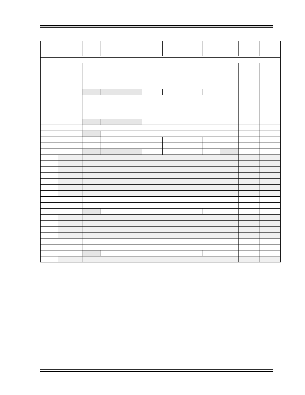
PIC16F/LF1946/47
TABLE 3-9: SPECIAL FUNCTION REGISTER SUMMARY (CONTINUED)
Address Name Bit 7 Bit 6 Bit 5 Bit 4 Bit 3 Bit 2 Bit 1 Bit 0
Bank 8
(2)
400h
401h
402h
403h
404h
405h
406h
407h
408h
409h
40Ah
40Bh
40Ch ANSELF ANSELF7 ANSELF6 ANSELF5 ANSELF4 ANSELF3 ANSELF2 ANSELF1 ANSELF0 1111 1111 1111 1111
40Dh ANSELG
40Eh
40Fh
410h
411h
412h
413h
414h
415h TMR4 Timer 4 Module Register 0000 0000 0000 0000
416h PR4 Timer 4 Period Register 1111 1111 1111 1111
417h T4CON
418h
419h
41Ah
41Bh
41Ch TMR6 Timer 6 Module Register 0000 0000 0000 0000
41Dh PR6 Timer 6 Period Register 1111 1111 1111 1111
41Eh T6CON
41Fh
Legend: x = unknown, u = unchanged, q = value depends on condition, - = unimplemented, read as ‘0’, r = reserved.
Note 1: The upper byte of the program counter is not directly accessible. PCLATH is a holding register for the PC<14:8>, whose contents are transferred
INDF0 Addressing this location uses contents of FSR0H/FSR0L to address data memory
(2)
INDF1 Addressing this location uses contents of FSR1H/FSR1L to address data memory
(2)
PCL Program Counter (PC) Least Significant Byte 0000 0000 0000 0000
(2)
STATUS — — —TOPD ZDCC---1 1000 ---q quuu
(2)
FSR0L Indirect Data Memory Address 0 Low Pointer 0000 0000 uuuu uuuu
(2)
FSR0H Indirect Data Memory Address 0 High Pointer 0000 0000 0000 0000
(2)
FSR1L Indirect Data Memory Address 1 Low Pointer 0000 0000 uuuu uuuu
(2)
FSR1H Indirect Data Memory Address 1 High Pointer 0000 0000 0000 0000
(2)
BSR — — — BSR<4:0> ---0 0000 ---0 0000
(2)
WREG Working Register 0000 0000 uuuu uuuu
(1, 2)
PCLATH — Write Buffer for the upper 7 bits of the Program Counter -000 0000 -000 0000
(2)
INTCON GIE PEIE TMR0IE INTE IOCIE TMR0IF INTF IOCIF 0000 000x 0000 000u
— Unimplemented — —
— Unimplemented — —
— Unimplemented — —
— Unimplemented — —
— Unimplemented — —
— Unimplemented — —
— Unimplemented — —
— Unimplemented — —
— Unimplemented — —
— Unimplemented — —
— Unimplemented — —
— Unimplemented — —
Shaded locations are unimplemented, read as ‘0’.
to the upper byte of the program counter.
2: These registers can be addressed from any bank.
(not a physical register)
(not a physical register)
— — — ANSELG4 ANSELG3 ANSELG2 ANSELG1 — ---1 111- ---1 111-
—
—
T4OUTPS<3:0>
T6OUTPS<3:0>
TMR4ON T4CKPS<1:0> -000 0000 -000 0000
TMR6ON T6CKPS<1:0> -000 0000 -000 0000
Value on:
POR, BOR
xxxx xxxx xxxx xxxx
xxxx xxxx xxxx xxxx
Value on all
other
Resets
2010 Microchip Technology Inc. Preliminary DS41414B-page 41

PIC16F/LF1946/47
TABLE 3-9: SPECIAL FUNCTION REGISTER SUMMARY (CONTINUED)
Address Name Bit 7 Bit 6 Bit 5 Bit 4 Bit 3 Bit 2 Bit 1 Bit 0
Bank 9
(2)
480h
481h
482h
483h
404h
485h
486h
487h
488h
489h
48Ah
48Bh
48Ch
48Dh WPUG
48Eh
48Fh
490h
491h RC2REG USART Receive Data Register 0000 0000 0000 0000
492h TX2REG USART Transmit Data Register 0000 0000 0000 0000
493h SP2BRGL EUSART2 Baud Rate Generator, Low Byte 0000 0000 0000 0000
494h SP2BRGH EUSART2 Baud Rate Generator, High Byte 0000 0000 0000 0000
495h RC2STA SPEN RX9 SREN CREN ADDEN FERR OERR RX9D 0000 000x 0000 000x
496h TX2STA CSRC TX9 TXEN SYNC SENDB BRGH TRMT TX9D 0000 0010 0000 0010
497h BAUDCON2 ABDOVF RCIDL
498h
499h
49Ah
49Bh
49Ch
49Dh
49Eh
49Fh
Legend: x = unknown, u = unchanged, q = value depends on condition, - = unimplemented, read as ‘0’, r = reserved.
Note 1: The upper byte of the program counter is not directly accessible. PCLATH is a holding register for the PC<14:8>, whose contents are transferred
INDF0 Addressing this location uses contents of FSR0H/FSR0L to address data memory
(2)
INDF1 Addressing this location uses contents of FSR1H/FSR1L to address data memory
(2)
PCL Program Counter (PC) Least Significant Byte 0000 0000 0000 0000
(2)
STATUS — — —TOPD ZDCC---1 1000 ---q quuu
(2)
FSR0L Indirect Data Memory Address 0 Low Pointer 0000 0000 uuuu uuuu
(2)
FSR0H Indirect Data Memory Address 0 High Pointer 0000 0000 0000 0000
(2)
FSR1L Indirect Data Memory Address 1 Low Pointer 0000 0000 uuuu uuuu
(2)
FSR1H Indirect Data Memory Address 1 High Pointer 0000 0000 0000 0000
(2)
BSR — — — BSR<4:0> ---0 0000 ---0 0000
(2)
WREG Working Register 0000 0000 uuuu uuuu
(1, 2)
PCLATH — Write Buffer for the upper 7 bits of the Program Counter -000 0000 -000 0000
(2)
INTCON GIE PEIE TMR0IE INTE IOCIE TMR0IF INTF IOCIF 0000 000x 0000 000u
— Unimplemented — —
— Unimplemented — —
— Unimplemented — —
— Unimplemented — —
— Unimplemented — —
— Unimplemented — —
— Unimplemented — —
— Unimplemented — —
— Unimplemented — —
— Unimplemented — —
— Unimplemented — —
— Unimplemented — —
Shaded locations are unimplemented, read as ‘0’.
to the upper byte of the program counter.
2: These registers can be addressed from any bank.
(not a physical register)
(not a physical register)
— —WPUG5— — — — — --1- ---- --1- ----
— SCKP BRG16 — WUE ABDEN 01-0 0-00 01-0 0-00
Value on:
POR, BOR
xxxx xxxx xxxx xxxx
xxxx xxxx xxxx xxxx
Value on all
other
Resets
DS41414B-page 42 Preliminary 2010 Microchip Technology Inc.

PIC16F/LF1946/47
TABLE 3-9: SPECIAL FUNCTION REGISTER SUMMARY (CONTINUED)
Address Name Bit 7 Bit 6 Bit 5 Bit 4 Bit 3 Bit 2 Bit 1 Bit 0
Banks 10-14
x00h/
x80h
x00h/
x81h
x02h/
x82h
x03h/
x83h
x04h/
x84h
x05h/
x85h
x06h/
x86h
x07h/
x87h
x08h/
x88h
x09h/
x89h
x0Ah/
x8Ah
x0Bh/
x8Bh
x0Ch/
x8Ch
—
x1Fh/
x9Fh
Legend: x = unknown, u = unchanged, q = value depends on condition, - = unimplemented, read as ‘0’, r = reserved.
Note 1: The upper byte of the program counter is not directly accessible. PCLATH is a holding register for the PC<14:8>, whose contents are transferred
INDF0 Addressing this location uses contents of FSR0H/FSR0L to address data memory
(2)
INDF1 Addressing this location uses contents of FSR1H/FSR1L to address data memory
(2)
PCL Program Counter (PC) Least Significant Byte 0000 0000 0000 0000
(2)
STATUS — — —TOPD ZDCC---1 1000 ---q quuu
(2)
FSR0L Indirect Data Memory Address 0 Low Pointer 0000 0000 uuuu uuuu
(2)
FSR0H Indirect Data Memory Address 0 High Pointer 0000 0000 0000 0000
(2)
FSR1L Indirect Data Memory Address 1 Low Pointer 0000 0000 uuuu uuuu
(2)
FSR1H Indirect Data Memory Address 1 High Pointer 0000 0000 0000 0000
(2)
BSR — — — BSR<4:0> ---0 0000 ---0 0000
(2)
WREG Working Register 0000 0000 uuuu uuuu
(2)
PCLATH — Write Buffer for the upper 7 bits of the Program Counter -000 0000 -000 0000
(1),(2)
INTCON GIE PEIE TMR0IE INTE IOCIE TMR0IF INTF IOCIF 0000 000x 0000 000u
(2)
— Unimplemented — —
Shaded locations are unimplemented, read as ‘0’.
to the upper byte of the program counter.
2: These registers can be addressed from any bank.
(not a physical register)
(not a physical register)
Value on:
POR, BOR
xxxx xxxx xxxx xxxx
xxxx xxxx xxxx xxxx
Value on all
other
Resets
2010 Microchip Technology Inc. Preliminary DS41414B-page 43

PIC16F/LF1946/47
TABLE 3-9: SPECIAL FUNCTION REGISTER SUMMARY (CONTINUED)
Address Name Bit 7 Bit 6 Bit 5 Bit 4 Bit 3 Bit 2 Bit 1 Bit 0
Bank 15
(2)
780h
781h
782h
783h
784h
785h
786h
787h
788h
789h
78Ah
78Bh
78Ch
78Dh
78Eh
78Fh
790h
791h LCDCON LCDEN SLPEN WERR
792h LCDPS WFT BIASMD LCDA WA LP
793h LCDREF LCDIRE LCDIRS LCDIRI
794h LCDCST
795h LCDRL LRLAP
796h
797h
798h LCDSE0 SE<7:0> 0000 0000 uuuu uuuu
799h LCDSE1 SE<15:8> 0000 0000 uuuu uuuu
79Ah LCDSE2 SE<23:16> 0000 0000 uuuu uuuu
79Bh LCDSE3 SE<31:24> 0000 0000 uuuu uuuu
79Ch LCDSE4 SE<39:32> 0000 0000 uuuu uuuu
79Dh LCDSE5
79Eh
79Fh
7A0h LCDDATA0 SEG7
7A1h LCDDATA1 SEG15
7A2h
7A3h LCDDATA3 SEG7
7A4h LCDDATA4 SEG15
7A5h
Legend: x = unknown, u = unchanged, q = value depends on condition, - = unimplemented, read as ‘0’, r = reserved.
Note 1: The upper byte of the program counter is not directly accessible. PCLATH is a holding register for the PC<14:8>, whose contents are transferred
INDF0 Addressing this location uses contents of FSR0H/FSR0L to address data memory
(2)
INDF1 Addressing this location uses contents of FSR1H/FSR1L to address data memory
(2)
PCL Program Counter (PC) Least Significant Byte 0000 0000 0000 0000
(2)
STATUS — — —TOPD ZDCC---1 1000 ---q quuu
(2)
FSR0L Indirect Data Memory Address 0 Low Pointer 0000 0000 uuuu uuuu
(2)
FSR0H Indirect Data Memory Address 0 High Pointer 0000 0000 0000 0000
(2)
FSR1L Indirect Data Memory Address 1 Low Pointer 0000 0000 uuuu uuuu
(2)
FSR1H Indirect Data Memory Address 1 High Pointer 0000 0000 0000 0000
(2)
BSR — — — BSR<4:0> ---0 0000 ---0 0000
(2)
WREG Working Register 0000 0000 uuuu uuuu
(1, 2)
PCLATH — Write Buffer for the upper 7 bits of the Program Counter -000 0000 -000 0000
(2)
INTCON GIE PEIE TMR0IE INTE IOCIE TMR0IF INTF IOCIF 0000 000x 0000 000u
— Unimplemented — —
— Unimplemented — —
— Unimplemented — —
— Unimplemented — —
— Unimplemented — —
— Unimplemented — —
— Unimplemented — —
— Unimplemented — —
— Unimplemented — —
LCDDATA2
LCDDATA5
Shaded locations are unimplemented, read as ‘0’.
to the upper byte of the program counter.
2: These registers can be addressed from any bank.
(not a physical register)
(not a physical register)
—CS<1:0> LMUX<1:0> 000- 0011 000- 0011
<3:0> 0000 0000 0000 0000
— VLCD3PE VLCD2PE VLCD1PE — 000- 000- 000- 000-
— — — — — LCDCST<2:0> ---- -000 ---- -000
<1:0> LRLBP<1:0> —LRLAT<2:0> 0000 -000 0000 -000
— — SE<45:40> --00 0000 --uu uuuu
COM0
COM0
SEG23
COM0
COM1
COM1
SEG23
COM1
SEG6
COM0
SEG14
COM0
SEG22
COM0
SEG6
COM1
SEG14
COM1
SEG22
COM1
SEG5
COM0
SEG13
COM0
SEG21
COM0
SEG5
COM1
SEG13
COM1
SEG21
COM1
SEG4
COM0
SEG12
COM0
SEG20
COM0
SEG4
COM1
SEG12
COM1
SEG20
COM1
SEG3
COM0
SEG11
COM0
SEG19
COM0
SEG3
COM1
SEG11
COM1
SEG19
COM1
SEG2
COM0
SEG10
COM0
SEG18
COM0
SEG2
COM1
SEG10
COM1
SEG18
COM1
SEG1
COM0
SEG9
COM0
SEG17
COM0
SEG1
COM1
SEG9
COM1
SEG17
COM1
SEG0
COM0
SEG8
COM0
SEG16
COM0
SEG0
COM1
SEG8
COM1
SEG16
COM1
Value on:
POR, BOR
xxxx xxxx xxxx xxxx
xxxx xxxx xxxx xxxx
xxxx xxxx uuuu uuuu
xxxx xxxx uuuu uuuu
xxxx xxxx uuuu uuuu
xxxx xxxx uuuu uuuu
xxxx xxxx uuuu uuuu
xxxx xxxx uuuu uuuu
Value on all
other
Resets
DS41414B-page 44 Preliminary 2010 Microchip Technology Inc.

PIC16F/LF1946/47
TABLE 3-9: SPECIAL FUNCTION REGISTER SUMMARY (CONTINUED)
Address Name Bit 7 Bit 6 Bit 5 Bit 4 Bit 3 Bit 2 Bit 1 Bit 0
Bank 15 (Continued)
7A6h LCDDATA6 SEG7
7A7h LCDDATA7 SEG15
7A8h
7A9h LCDDATA9 SEG7
7AAh LCDDATA10 SEG15
7ABh
7ACh
7ADh
7AEh
7AFh
7B0h
7B1h
7B2h
7B3h
7B4h
7B5h
7B6h
7B7h
7B8h
—
7EFh
Legend: x = unknown, u = unchanged, q = value depends on condition, - = unimplemented, read as ‘0’, r = reserved.
Note 1: The upper byte of the program counter is not directly accessible. PCLATH is a holding register for the PC<14:8>, whose contents are transferred
LCDDATA8
LCDDATA11
LCDDATA12
LCDDATA13
LCDDATA14
LCDDATA15
LCDDATA16
LCDDATA17
LCDDATA18
LCDDATA19
LCDDATA20
LCDDATA21
LCDDATA22
LCDDATA23
— Unimplemented — —
Shaded locations are unimplemented, read as ‘0’.
to the upper byte of the program counter.
2: These registers can be addressed from any bank.
COM2
COM2
SEG23
COM2
COM3
COM3
SEG23
COM3
SEG31
COM0
SEG39
COM0
— —SEG45
SEG31
COM1
SEG39
COM1
— —SEG45
SEG31
COM2
SEG39
COM2
— —SEG45
SEG31
COM3
SEG39
COM3
— —SEG45
SEG6
COM2
SEG14
COM2
SEG22
COM2
SEG6
COM3
SEG14
COM3
SEG22
COM3
SEG30
COM0
SEG38
COM0
SEG30
COM1
SEG38
COM1
SEG30
COM2
SEG38
COM2
SEG30
COM3
SEG38
COM3
SEG5
COM2
SEG13
COM2
SEG21
COM2
SEG5
COM3
SEG13
COM3
SEG21
COM3
SEG29
COM0
SEG37
COM0
COM0
SEG29
COM1
SEG37
COM1
COM1
SEG29
COM2
SEG37
COM2
COM2
SEG29
COM3
SEG37
COM3
COM3
SEG4
COM2
SEG12
COM2
SEG20
COM2
SEG4
COM3
SEG12
COM3
SEG20
COM3
SEG28
COM0
SEG36
COM0
SEG44
COM0
SEG28
COM1
SEG36
COM1
SEG44
COM1
SEG28
COM2
SEG36
COM2
SEG44
COM2
SEG28
COM3
SEG36
COM3
SEG44
COM3
SEG3
COM2
SEG11
COM2
SEG19
COM2
SEG3
COM3
SEG11
COM3
SEG19
COM3
SEG27
COM0
SEG35
COM0
SEG43
COM0
SEG27
COM1
SEG35
COM1
SEG43
COM1
SEG27
COM2
SEG35
COM2
SEG43
COM2
SEG27
COM3
SEG35
COM3
SEG43
COM3
SEG2
COM2
SEG10
COM2
SEG18
COM2
SEG2
COM3
SEG10
COM3
SEG18
COM3
SEG26
COM0
SEG34
COM0
SEG42
COM0
SEG26
COM1
SEG34
COM1
SEG42
COM1
SEG26
COM2
SEG34
COM2
SEG42
COM2
SEG26
COM3
SEG34
COM3
SEG42
COM3
SEG1
COM2
SEG9
COM2
SEG17
COM2
SEG1
COM3
SEG9
COM3
SEG17
COM3
SEG25
COM0
SEG33
COM0
SEG41
COM0
SEG25
COM1
SEG33
COM1
SEG41
COM1
SEG25
COM2
SEG33
COM2
SEG41
COM2
SEG25
COM3
SEG33
COM3
SEG41
COM3
SEG0
COM2
SEG8
COM2
SEG16
COM2
SEG0
COM3
SEG8
COM3
SEG16
COM3
SEG24
COM0
SEG32
COM0
SEG40
COM0
SEG24
COM1
SEG32
COM1
SEG40
COM1
SEG24
COM2
SEG32
COM2
SEG40
COM2
SEG24
COM3
SEG32
COM3
SEG40
COM3
Value on:
POR, BOR
xxxx xxxx uuuu uuuu
xxxx xxxx uuuu uuuu
xxxx xxxx uuuu uuuu
xxxx xxxx uuuu uuuu
xxxx xxxx uuuu uuuu
xxxx xxxx uuuu uuuu
xxxx xxxx uuuu uuuu
xxxx xxxx uuuu uuuu
--xx xxxx --uu uuuu
xxxx xxxx uuuu uuuu
xxxx xxxx uuuu uuuu
--xx xxxx --uu uuuu
xxxx xxxx uuuu uuuu
xxxx xxxx uuuu uuuu
--xx xxxx --uu uuuu
xxxx xxxx uuuu uuuu
xxxx xxxx uuuu uuuu
--xx xxxx --uu uuuu
Value on all
other
Resets
2010 Microchip Technology Inc. Preliminary DS41414B-page 45

PIC16F/LF1946/47
TABLE 3-9: SPECIAL FUNCTION REGISTER SUMMARY (CONTINUED)
Address Name Bit 7 Bit 6 Bit 5 Bit 4 Bit 3 Bit 2 Bit 1 Bit 0
Banks 16-30
x00h/
x80h
x00h/
x81h
x02h/
x82h
x03h/
x83h
x04h/
x84h
x05h/
x85h
x06h/
x86h
x07h/
x87h
x08h/
x88h
x09h/
x89h
x0Ah/
x8Ah
x0Bh/
x8Bh
x0Ch/
x8Ch
—
x1Fh/
x9Fh
Legend: x = unknown, u = unchanged, q = value depends on condition, - = unimplemented, read as ‘0’, r = reserved.
Note 1: The upper byte of the program counter is not directly accessible. PCLATH is a holding register for the PC<14:8>, whose contents are transferred
INDF0 Addressing this location uses contents of FSR0H/FSR0L to address data memory
(2)
INDF1 Addressing this location uses contents of FSR1H/FSR1L to address data memory
(2)
PCL Program Counter (PC) Least Significant Byte 0000 0000 0000 0000
(2)
STATUS — — —TOPD ZDCC---1 1000 ---q quuu
(2)
FSR0L Indirect Data Memory Address 0 Low Pointer 0000 0000 uuuu uuuu
(2)
FSR0H Indirect Data Memory Address 0 High Pointer 0000 0000 0000 0000
(2)
FSR1L Indirect Data Memory Address 1 Low Pointer 0000 0000 uuuu uuuu
(2)
FSR1H Indirect Data Memory Address 1 High Pointer 0000 0000 0000 0000
(2)
BSR — — — BSR<4:0> ---0 0000 ---0 0000
(2)
WREG Working Register 0000 0000 uuuu uuuu
(2)
PCLATH — Write Buffer for the upper 7 bits of the Program Counter -000 0000 -000 0000
(1),(2)
INTCON GIE PEIE TMR0IE INTE IOCIE TMR0IF INTF IOCIF 0000 000x 0000 000u
(2)
— Unimplemented — —
Shaded locations are unimplemented, read as ‘0’.
to the upper byte of the program counter.
2: These registers can be addressed from any bank.
(not a physical register)
(not a physical register)
Value on:
POR, BOR
xxxx xxxx xxxx xxxx
xxxx xxxx xxxx xxxx
Value on all
other
Resets
DS41414B-page 46 Preliminary 2010 Microchip Technology Inc.

PIC16F/LF1946/47
TABLE 3-9: SPECIAL FUNCTION REGISTER SUMMARY (CONTINUED)
Address Name Bit 7 Bit 6 Bit 5 Bit 4 Bit 3 Bit 2 Bit 1 Bit 0
Bank 31
(2)
F80h
F81h
F82h
F83h
F84h
F85h
F86h
F87h
F88h
F89h
F8Ah
)
F8Bh
F8Ch
—
FE3h
FE4h STATUS_
FE5h WREG_
FE6h BSR_
FE7h PCLATH_
FE8h FSR0L_
FE9h FSR0H_
FEAh FSR1L_
FEBh FSR1H_
FECh
FEDh
FEEh
FEFh
Legend: x = unknown, u = unchanged, q = value depends on condition, - = unimplemented, read as ‘0’, r = reserved.
Note 1: The upper byte of the program counter is not directly accessible. PCLATH is a holding register for the PC<14:8>, whose contents are transferred
INDF0 Addressing this location uses contents of FSR0H/FSR0L to address data memory
(2)
INDF1 Addressing this location uses contents of FSR1H/FSR1L to address data memory
(2)
PCL Program Counter (PC) Least Significant Byte 0000 0000 0000 0000
(2)
STATUS — — —TOPD ZDCC---1 1000 ---q quuu
(2)
FSR0L Indirect Data Memory Address 0 Low Pointer 0000 0000 uuuu uuuu
(2)
FSR0H Indirect Data Memory Address 0 High Pointer 0000 0000 0000 0000
(2)
FSR1L Indirect Data Memory Address 1 Low Pointer 0000 0000 uuuu uuuu
(2)
FSR1H Indirect Data Memory Address 1 High Pointer 0000 0000 0000 0000
(2)
BSR — — — BSR<4:0> ---0 0000 ---0 0000
(2)
WREG Working Register 0000 0000 uuuu uuuu
(1),(2
PCLATH — Write Buffer for the upper 7 bits of the Program Counter -000 0000 -000 0000
(2)
INTCON GIE PEIE TMR0IE INTE IOCIE TMR0IF INTF IOCIF 0000 000x 0000 000u
— Unimplemented — —
SHAD
SHAD
SHAD
SHAD
SHAD
SHAD
SHAD
SHAD
— Unimplemented — —
STKPTR
TOSL
TOSH
Shaded locations are unimplemented, read as ‘0’.
to the upper byte of the program counter.
2: These registers can be addressed from any bank.
(not a physical register)
(not a physical register)
ZDCC---- -xxx ---- -uuu
Working Register Normal (Non-ICD) Shadow xxxx xxxx uuuu uuuu
Bank Select Register Normal (Non-ICD) Shadow ---x xxxx ---u uuuu
Program Counter Latch High Register Normal (Non-ICD) Shadow -xxx xxxx uuuu uuuu
Indirect Data Memory Address 0 Low Pointer Normal (Non-ICD) Shadow xxxx xxxx uuuu uuuu
Indirect Data Memory Address 0 High Pointer Normal (Non-ICD) Shadow xxxx xxxx uuuu uuuu
Indirect Data Memory Address 1 Low Pointer Normal (Non-ICD) Shadow xxxx xxxx uuuu uuuu
Indirect Data Memory Address 1 High Pointer Normal (Non-ICD) Shadow xxxx xxxx uuuu uuuu
— — — Current Stack pointer ---1 1111 ---1 1111
Top of Stack Low byte xxxx xxxx uuuu uuuu
— Top of Stack High byte -xxx xxxx -uuu uuuu
Value on:
POR, BOR
xxxx xxxx xxxx xxxx
xxxx xxxx xxxx xxxx
Value on all
other
Resets
2010 Microchip Technology Inc. Preliminary DS41414B-page 47

PIC16F/LF1946/47
PCLPCH
0
14
PC
06
7
ALU Result
8
PCLATH
PCLPCH
0
14
PC
06
4
OPCODE <10:0>
11
PCLATH
PCLPCH
0
14
PC
06
7
W
8
PCLATH
Instruction with
PCL as
Destination
GOTO, CALL
CALLW
PCL
PCH
0
14
PC
PC + W
15
BRW
PCLPCH
0
14
PC
PC + OPCODE <8:0>
15
BRA
3.3 PCL and PCLATH
The Program Counter (PC) is 15 bits wide. The low byte
comes from the PCL register, which is a readable and
writable register. The high byte (PC<14:8>) is not directly
readable or writable and comes from PCLATH. On any
Reset, the PC is cleared. Figure 3-4 shows the five
situations for the loading of the PC.
FIGURE 3-4: LOADING OF PC IN
DIFFERENT SITUATIONS
3.3.3 COMPUTED FUNCTION CALLS
A computed function CALL allows programs to maintain
tables of functions and provide another way to execute
state machines or look-up tables. When performing a
table read using a computed function CALL, care
should be exercised if the table location crosses a PCL
memory boundary (each 256-byte block).
If using the CALL instruction, the PCH<2:0> and PCL
registers are loaded with the operand of the CALL
instruction. PCH<6:3> is loaded with PCLATH<6:3>.
The CALLW instruction enables computed calls by combining PCLATH and W to form the destination address.
A computed CALLW is accomplished by loading the W
register with the desired address and executing CALLW.
The PCL register is loaded with the value of W and
PCH is loaded with PCLATH.
3.3.4 BRANCHING
The branching instructions add an offset to the PC.
This allows relocatable code and code that crosses
page boundaries. There are two forms of branching,
BRW and BRA. The PC will have incremented to fetch
the next instruction in both cases. When using either
branching instruction, a PCL memory boundary may be
crossed.
If using BRW, load the W register with the desired
unsigned address and execute BRW. The entire PC will
be loaded with the address PC + 1 + W.
If using BRA, the entire PC will be loaded with PC + 1 +,
the signed value of the operand of the BRA instruction.
3.3.1 MODIFYING PCL
Executing any instruction with the PCL register as the
destination simultaneously causes the Program Counter PC<14:8> bits (PCH) to be replaced by the contents
of the PCLATH register. This allows the entire contents
of the program counter to be changed by writing the
desired upper 7 bits to the PCLATH register. When the
lower 8 bits are written to the PCL register, all 15 bits of
the program counter will change to the values contained in the PCLATH register and those being written
to the PCL register.
3.3.2 COMPUTED GOTO
A computed GOTO is accomplished by adding an offset to
the program counter (ADDWF PC L). When performing a
table read using a computed GOTO method, care should
be exercised if the table location crosses a PCL memory
boundary (each 256-byte block). Refer to the Application
Note AN556, “Implementing a T able Read” (DS00556).
DS41414B-page 48 Preliminary 2010 Microchip Technology Inc.

PIC16F/LF1946/47
0x0F
0x0E
0x0D
0x0C
0x0B
0x0A
0x09
0x08
0x07
0x06
0x05
0x04
0x03
0x02
0x01
0x00
0x0000
STKPTR = 0x1F
Initial Stack Configuration:
After Reset, the stack is empty. The
empty stack is initialized so the Stack
Pointer is pointing at 0x1F. If the Stack
Overflow/Underflow Reset is enabled, the
TOSH/TOSL registers will return ‘0’. If
the Stack Overflow/Underflow Reset is
disabled, the TOSH/TOSL registers will
return the contents of stack address 0x0F.
0x1F STKPTR = 0x1F
Stack Reset Disabled
(STVREN = 0)
Stack Reset Enabled
(STVREN = 1)
TOSH:TOSL
TOSH:TOSL
3.4 Stack
All devices have a 16-level x 15-bit wide hardware
stack (refer to Figures 3-3 and 3-4). The stack space is
not part of either program or data space. The PC is
PUSHed onto the stack when CALL or CALLW instructions are executed or an interrupt causes a branch. The
stack is POPed in the event of a RETURN, RETLW or a
RETFIE instruction execution. PCLATH is not affected
by a PUSH or POP operation.
The stack operates as a circular buffer if the STVREN
bit is programmed to ‘0‘ (Configuration Word 2). This
means that after the stack has been PUSHed sixteen
times, the seventeenth PUSH overwrites the value that
was stored from the first PUSH. The eighteenth PUSH
overwrites the second PUSH (and so on). The
STKOVF and STKUNF flag bits will be set on an Overflow/Underflow, regardless of whether the Reset is
enabled.
Note 1: There are no instructions/mnemonics
called PUSH or POP. These are actions
that occur from the execution of the
CALL, CALLW, RETURN, RETLW and
RETFIE instructions or the vectoring to
an interrupt address.
3.4.1 ACCESSING THE STACK
The stack is available through the TOSH, TOSL and
STKPTR registers. STKPTR is the current value of the
Stack Pointer. TOSH:TOSL register pair points to the
TOP of the stack. Both registers are read/writable. TOS
is split into TOSH and TOSL due to the 15-bit size of the
PC. To access the stack, adjust the value of STKPTR,
which will position TOSH:TOSL, then read/write to
TOSH:TOSL. STKPTR is 5 bits to allow detection of
overflow and underflow.
Note: Care should be taken when modifying the
STKPTR while interrupts are enabled.
During normal program operation, CALL, CALLW and
Interrupts will increment STKPTR while RETLW,
RETURN, and RETFIE will decrement STKPTR. At any
time STKPTR can be inspected to see how much stack
is left. The STKPTR always points at the currently used
place on the stack. Therefore, a CALL or CALLW will
increment the STKPTR and then write the PC, and a
return will unload the PC and then decrement the STKPTR.
Reference Figure through Figure for examples of
accessing the stack.
FIGURE 3-5: ACCESSING THE STACK EXAMPLE 1
2010 Microchip Technology Inc. Preliminary DS41414B-page 49

PIC16F/LF1946/47
0x0F
0x0E
0x0D
0x0C
0x0B
0x0A
0x09
0x08
0x07
0x06
0x05
0x04
0x03
0x02
0x01
Return Address0x00
STKPTR = 0x00
This figure shows the stack configuration
after the first CALL or a single interrupt.
If a RETURN instruction is executed, the
return address will be placed in the
Program Counter and the Stack Pointer
decremented to the empty state (0x1F).
TOSH:TOSL
0x0F
0x0E
0x0D
0x0C
0x0B
0x0A
0x09
0x08
0x07
Return Address0x06
Return Address0x05
Return Address0x04
Return Address0x03
Return Address0x02
Return Address0x01
Return Address0x00
STKPTR = 0x06
After seven CALLs or six CALLs and an
interrupt, the stack looks like the figure
on the left. A series of RETURN instructions
will repeatedly place the return addresses
into the Program Counter and pop the stack.
TOSH:TOSL
FIGURE 3-6: ACCESSING THE STACK EXAMPLE 2
FIGURE 3-7: ACCESSING THE STACK EXAMPLE 3
DS41414B-page 50 Preliminary 2010 Microchip Technology Inc.

FIGURE 3-8: ACCESSING THE STACK EXAMPLE 4
0x0F
0x0E
0x0D
0x0C
0x0B
0x0A
0x09
0x08
0x07
0x06
0x05
0x04
0x03
0x02
0x01
Return Address0x00 STKPTR = 0x10
When the stack is full, the next CALL or
an interrupt will set the Stack Pointer to
0x10. This is identical to address 0x00
so the stack will wrap and overwrite the
return address at 0x00. If the Stack
Overflow/Underflow Reset is enabled, a
Reset will occur and location 0x00 will
not be overwritten.
Return Address
Return Address
Return Address
Return Address
Return Address
Return Address
Return Address
Return Address
Return Address
Return Address
Return Address
Return Address
Return Address
Return Address
Return Address
TOSH:TOSL
PIC16F/LF1946/47
3.4.2 OVERFLOW/UNDERFLOW RESET
If the STVREN bit in Configuration Word 2 is
programmed to ‘1’, the device will be reset if the stack
is PUSHed beyond the sixteenth level or POPed
beyond the first level, setting the appropriate bits
(STKOVF or STKUNF, respectively) in the PCON
register.
3.5 Indirect Addressing
The INDFn registers are not physical registers. Any
instruction that accesses an INDFn register actually
accesses the register at the address specified by the
File Select Registers (FSR). If the FSRn address
specifies one of the two INDFn registers, the read will
return ‘0’ and the write will not occur (though Status bits
may be affected). The FSRn register value is created
by the pair FSRnH and FSRnL.
The FSR registers form a 16-bit address that allows an
addressing space with 65536 locations. These locations
are divided into three memory regions:
• Traditional Data Memory
• Linear Data Memory
• Program Flash Memory
2010 Microchip Technology Inc. Preliminary DS41414B-page 51

PIC16F/LF1946/47
0x0000
0x0FFF
Traditional
FSR
Address
Range
Data Memory
0x1000
Reserved
Linear
Data Memory
Reserved
0x2000
0x29AF
0x29B0
0x7FFF
0x8000
0xFFFF
0x0000
0x0FFF
0x0000
0x7FFF
Program
Flash Memory
Note: Not all memory regions are completely implemented. Consult device memory tables for memory limits.
0x1FFF
FIGURE 3-9: INDIRECT ADDRESSING
DS41414B-page 52 Preliminary 2010 Microchip Technology Inc.

3.5.1 TRADITIONAL DATA MEMORY
Indirect AddressingDirect Addressing
Bank Select
Location Select
4BSR 6
0
From Opcode
FSRxL70
Bank Select
Location Select
00000 00001 00010 11111
0x00
0x7F
Bank 0 Bank 1 Bank 2 Bank 31
0
FSRxH70
0000
The traditional data memory is a region from FSR
address 0x000 to FSR address 0xFFF. The addresses
correspond to the absolute addresses of all SFR, GPR
and common registers.
FIGURE 3-10: TRADITIONAL DATA MEMORY MAP
PIC16F/LF1946/47
2010 Microchip Technology Inc. Preliminary DS41414B-page 53

PIC16F/LF1946/47
7
0
1
7
0
0
Location Select
0x2000
FSRnH
FSRnL
0x020
Bank 0
0x06F
0x0A0
Bank 1
0x0EF
0x120
Bank 2
0x16F
0xF20
Bank 30
0xF6F
0x29AF
0
7
1
7
0
0
Location Select
0x8000
FSRnH
FSRnL
0x0000
0x7FFF
0xFFFF
Program
Flash
Memory
(low 8
bits)
3.5.2 LINEAR DATA MEMORY
The linear data memory is the region from FSR
address 0x2000 to FSR address 0x29AF. This region is
a virtual region that points back to the 80-byte blocks of
GPR memory in all the banks.
Unimplemented memory reads as 0x00. Use of the
linear data memory region allows buffers to be larger
than 80 bytes because incrementing the FSR beyond
one bank will go directly to the GPR memory of the next
bank.
The 16 bytes of common memory are not included in
the linear data memory region.
FIGURE 3-11: LINEAR DATA MEMORY
MAP
3.5.3 PROGRAM FLASH MEMORY
To make constant data access easier, the entire
program Flash memory is mapped to the upper half of
the FSR address space. When the MSB of FSRnH is
set, the lower 15 bits are the address in program
memory which will be accessed through INDF. Only the
lower 8 bits of each memory location is accessible via
INDF. Writing to the program Flash memory cannot be
accomplished via the FSR/INDF interface. All
instructions that access program Flash memory via the
FSR/INDF interface will require one additional
instruction cycle to complete.
FIGURE 3-12: PROGRAM FLASH
MEMORY MAP
DS41414B-page 54 Preliminary 2010 Microchip Technology Inc.

4.0 DEVICE CONFIGURATION
Device Configuration consists of Configuration Word 1
and Configuration Word 2 registers, Code Protection
and Device ID.
4.1 Configuration Words
There are several Configuration Word bits that allow
different oscillator and memory protection options.
These are implemented as Configuration Word 1 at
8007h and Configuration Word 2 at 8008h.
Note: The DEBUG bit in Configuration Word 2 is
managed automatically by device
development tools including debuggers
and programmers. For normal device
operation, this bit should be maintained as
a '1'.
PIC16F/LF1946/47
2010 Microchip Technology Inc. Preliminary DS41414B-page 55
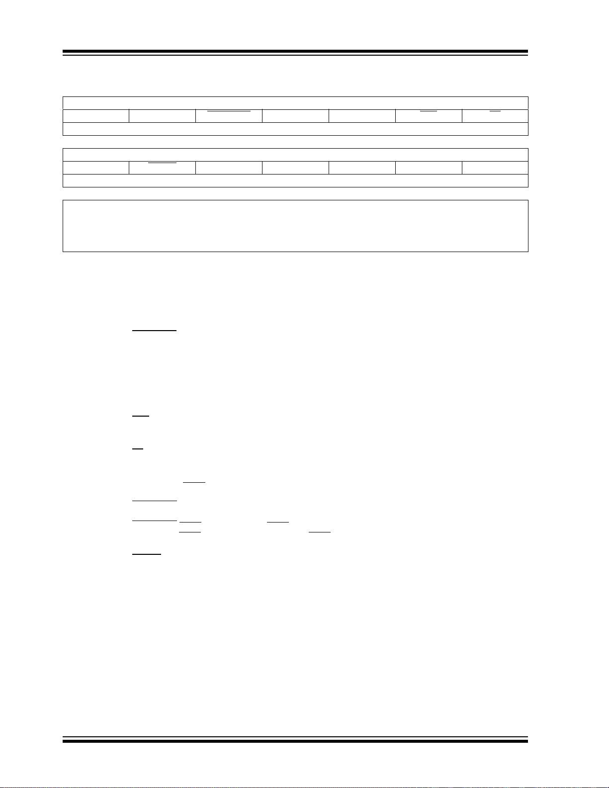
PIC16F/LF1946/47
REGISTER 4-1: CONFIGURATION WORD 1
R/P-1/1 R/P-1/1 R/P-1/1 R/P-1/1 R/P-1/1 R/P-1/1 R/P-1/1
FCMEN IESO CLKOUTEN
bit 13 bit 7
R/P-1/1 R/P-1/1 R/P-1/1 R/P-1/1 R/P-1/1 R/P-1/1 R/P-1/1
MCLRE PWRTE
bit 6 bit 0
Legend:
R = Readable bit W = Writable bit U = Unimplemented bit, read as ‘1’
u = Bit is unchanged x = Bit is unknown -n/n = Value at POR and BOR/Value at all other Resets
‘1’ = Bit is set ‘0’ = Bit is cleared P = Programmable bit
bit 13 FCMEN: Fail-Safe Clock Monitor Enable bit
1 = Fail-Safe Clock Monitor is enabled
0 = Fail-Safe Clock Monitor is disabled
bit 12 IESO: Internal External Switchover bit
1 = Internal/External Switchover mode is enabled
0 = Internal/External Switchover mode is disabled
bit 11 CLKOUTEN
1 = CLKOUT function is disabled. I/O or oscillator function on RA6/CLKOUT
0 = CLKOUT function is enabled on RA6/CLKOUT
bit 10-9 BOREN<1:0>: Brown-out Reset Enable bits
11 = BOR enabled
10 = BOR enabled during operation and disabled in Sleep
01 = BOR controlled by SBOREN bit of the BORCON register
00 = BOR disabled
bit 8 CPD
bit 7 CP
bit 6 MCLRE: RE3/MCLR
bit 5 PWRTE
bit 4-3 WDTE<1:0>: Watchdog Timer Enable bit
1 = Data memory code protection is disabled
0 = Data memory code protection is enabled
: Code Protection bit
1 = Program memory code protection is disabled
0 = Program memory code protection is enabled
If LVP bit =
If LVP bit =
1 = PWRT disabled
0 = PWRT enabled
11 = WDT enabled
10 = WDT enabled while running and disabled in Sleep
01 = WDT controlled by the SWDTEN bit in the WDTCON register
00 = WDT disabled
: Clock Out Enable bit
: Data Code Protection bit
1:
This bit is ignored.
0:
1 =RE3/MCLR
0 = RE3/MCLR
bit.
: Power-up Timer Enable bit
WDTE1 WDTE0 FOSC2 FOSC1 FOSC0
(2)
(3)
/VPP Pin Function Select bit
/VPP pin function is MCLR; Weak pull-up enabled.
/VPP pin function is digital input; MCLR internally disabled; Weak pull-up under control of WPUE3
BOREN1 BOREN0 CPD CP
(1)
(1)
Note 1: Enabling Brown-out Reset does not automatically enable Power-up Timer.
2: The entire data EEPROM will be erased when the code protection is turned off during an erase.
3: The entire program memory will be erased when the code protection is turned off.
DS41414B-page 56 Preliminary 2010 Microchip Technology Inc.

REGISTER 4-1: CONFIGURATION WORD 1 (CONTINUED)
PIC16F/LF1946/47
bit 2-0 FOSC<2:0>: Oscillator Selection bits
Note 1: Enabling Brown-out Reset does not automatically enable Power-up Timer.
2: The entire data EEPROM will be erased when the code protection is turned off during an erase.
3: The entire program memory will be erased when the code protection is turned off.
111 = ECH: External Clock, High-Power mode: CLKIN on RA7/OSC1/CLKIN
110 = ECM: External Clock, Medium-Power mode: CLKIN on RA7/OSC1/CLKIN
101 = ECL: External Clock, Low-Power mode: CLKIN on RA7/OSC1/CLKIN
100 = INTOSC oscillator: I/O function on RA7/OSC1/CLKIN
011 = EXTRC oscillator: RC function on RA7/OSC1/CLKIN
010 = HS oscillator: High-speed crystal/resonator on RA6/OSC2/CLKOUT pin and RA7/OSC1/CLKIN
001 = XT oscillator: Crystal/resonator on RA6/OSC2/CLKOUT pin and RA7/OSC1/CLKIN
000 = LP oscillator: Low-power crystal on RA6/OSC2/CLKOUT pin and RA7/OSC1/CLKIN
2010 Microchip Technology Inc. Preliminary DS41414B-page 57

PIC16F/LF1946/47
REGISTER 4-2: CONFIGURATION WORD 2
R/P-1/1 R/P-1/1 U-1 R/P-1/1 R/P-1/1 R/P-1/1 U-1
LVP DEBUG
bit 13 bit 7
U-1 U-1 R/P-1/1 U-1 U-1 R/P-1/1 R/P-1/1
— —VCAPEN— —WRT1WRT0
bit 6 bit 0
Legend:
R = Readable bit W = Writable bit U = Unimplemented bit, read as ‘0’
u = Bit is unchanged x = Bit is unknown -n/n = Value at POR and BOR/Value at all other Resets
‘1’ = Bit is set ‘0’ = Bit is cleared P = Programmable bit
bit 13 LVP: Low-Voltage Programming Enable bit
1 = Low-voltage programming enabled
0 = High-voltage on MCLR
bit 12 DEBUG
1 = In-Circuit Debugger disabled, RB6/ICSPCLK and RB7/ICSPDAT are general purpose I/O pins
0 = In-Circuit Debugger enabled, RB6/ICSPCLK and RB7/ICSPDAT are dedicated to the debugger
bit 11 Unimplemented: Read as ‘1’
bit 10 BORV: Brown-out Reset Voltage Selection bit
1 = Brown-out Reset voltage set to 1.9V
0 = Brown-out Reset voltage set to 2.5V
bit 9 STVREN: Stack Overflow/Underflow Reset Enable bit
1 = Stack Overflow or Underflow will cause a Reset
0 = Stack Overflow or Underflow will not cause a Reset
bit 8 PLLEN: PLL Enable bit
1 = 4xPLL enabled
0 = 4xPLL disabled
bit 7-5 Unimplemented: Read as ‘1’
bit 4 VCAPEN>: Voltage Regulator Capacitor Enable bits
0 =V
1 = No capacitor on V
bit 2-3 Unimplemented: Read as ‘1’
bit 1-0 WRT<1:0>: Flash Memory Self-Write Protection bits
8 kW Flash memory (PIC16F/LF1946 only)
16 kW Flash memory (PIC16F/LF1947)
(2)
: In-Circuit Debugger Mode bit
CAP functionality is enabled on RF0
11 = Write protection off
10 = 000h to 1FFh write-protected, 200h to 1FFFh may be modified by EECON control
01 = 000h to FFFh write-protected, 1000h to 1FFFh may be modified by EECON control
00 = 000h to 1FFFh write-protected, no addresses may be modified by EECON control
11 = Write protection off
10 = 000h to 1FFh write-protected, 200h to 3FFFh may be modified by EECON control
01 = 000h to 1FFFh write-protected, 2000h to 3FFFh may be modified by EECON control
00 = 000h to 3FFFh write-protected, no addresses may be modified by EECON control
— BORV STVREN PLLEN —
(1)
/VPP must be used for programming
CAP pin
:
:
Note 1: The LVP bit cannot be programmed to ‘0’ when Programming mode is entered via LVP.
2: The DEBUG
programmers. For normal device operation, this bit should be maintained as a '1'.
DS41414B-page 58 Preliminary 2010 Microchip Technology Inc.
bit in Configuration Word is managed automatically by device development tools including debuggers and

4.2 Code Protection
Code protection allows the device to be protected from
unauthorized access. Program memory protection and
data EEPROM protection are controlled independently.
Internal access to the program memory and data
EEPROM are unaffected by any code protection
setting.
4.2.1 PROGRAM MEMORY PROTECTION
The entire program memory space is protected from
external reads and writes by the CP
Word 1. When CP
program memory are inhibited and a read will return all
‘0’s. The CPU can continue to read program memory,
regardless of the protection bit settings. Writing the
program memory is dependent upon the write
protection setting. See Section 4.3 “Write
Protection” for more information.
= 0, external reads and writes of
4.2.2 DATA EEPROM PROTECTION
The entire data EEPROM is protected from external
reads and writes by the CPD
external reads and writes of data EEPROM are
inhibited. The CPU can continue to read and write data
EEPROM regardless of the protection bit settings.
bit in Configuration
bit. When CPD = 0,
PIC16F/LF1946/47
4.3 Write Protection
Write protection allows the device to be protected from
unintended self-writes. Applications, such as
bootloader software, can be protected while allowing
other regions of the program memory to be modified.
The WRT<1:0> bits in Configuration Word 2 define the
size of the program memory block that is protected.
4.4 User ID
Four memory locations (8000h-8003h) are designated
as ID locations where the user can store checksum or
other code identification numbers. These locations are
readable and writable during normal execution. See
Section 4.5 “Device ID and Revision ID” for more
information on accessing these memory locations.
more information on checksum calculation, see the
“PIC16F193X/LF193X/PIC16F194X/LF194X Memory
Programming Specification” (DS41397).
For
2010 Microchip Technology Inc. Preliminary DS41414B-page 59

PIC16F/LF1946/47
4.5 Device ID and Revision ID
The memory location 8006h is where the Device ID and
Revision ID are stored. The upper nine bits hold the
Device ID. The lower five bits hold the Revision ID. See
Section 11.5 “User ID, Device ID and Configuration
Word Access” for more information on accessing
these memory locations.
Development tools, such as device programmers and
debuggers, may be used to read the Device ID and
Revision ID.
REGISTER 4-3: DEVICEID: DEVICE ID REGISTER
RRRRRRR
DEV8 DEV7 DEV6 DEV5 DEV4 DEV3 DEV2
bit 13 bit 7
RRRRRRR
DEV1 DEV0 REV4 REV3 REV2 REV1 REV0
bit 6 bit 0
(1)
Legend: U = Unimplemented bit, read as ‘0’
R = Readable bit W = Writable bit ‘0’ = Bit is cleared
-n = Value at POR ‘1’ = Bit is set x = Bit is unknown
bit 13-5 DEV<8:0>: Device ID bits
100011001 = PIC16F1946
100011010 = PIC16F1947
100011011 = PIC16LF1946
100011100 = PIC16LF1947
bit 4-0 REV<4:0>: Revision ID bits
These bits are used to identify the revision.
Note 1: This location cannot be written.
DS41414B-page 60 Preliminary 2010 Microchip Technology Inc.

PIC16F/LF1946/47
5.0 OSCILLATOR MODULE (WITH FAIL-SAFE CLOCK MONITOR)
5.1 Overview
The oscillator module has a wide variety of clock
sources and selection features that allow it to be used
in a wide range of applications while maximizing performance and minimizing power consumption. Figure 5-1
illustrates a block diagram of the oscillator module.
Clock sources can be supplied from external oscillators,
quartz crystal resonators, ceramic resonators and
Resistor-Capacitor (RC) circuits. In addition, the system
clock source can be supplied from one of two internal
oscillators and PLL circuits, with a choice of speeds
selectable via software. Additional clock features
include:
• Selectable system clock source between external
or internal sources via software.
• Two-Speed Start-up mode, which minimizes
latency between external oscillator start-up and
code execution.
• Fail-Safe Clock Monitor (FSCM) designed to
detect a failure of the external clock source (LP,
XT, HS, EC or RC modes) and switch
automatically to the internal oscillator.
• Oscillator Start-up Timer (OST) ensures stability
of crystal oscillator sources
The oscillator module can be configured in one of eight
clock modes.
1. ECL – External Clock Low Power mode
(0 MHz to 0.5 MHz)
2. ECM – External Clock Medium Power mode
(0.5 MHz to 4 MHz)
3. ECH – External Clock High Power mode
(4 MHz to 32 MHz)
4. LP – 32 kHz Low-Power Crystal mode.
5. XT – Medium Gain Crystal or Ceramic Resonator
Oscillator mode (up to 4 MHz)
6. HS – High Gain Crystal or Ceramic Resonator
mode (4 MHz to 20 MHz)
7. RC – External Resistor-Capacitor (RC).
8. INTOSC – Internal oscillator (31 kHz to 32 MHz).
Clock Source modes are selected by the FOSC<2:0>
bits in the Configuration Word 1. The FOSC bits
determine the type of oscillator that will be used when
the device is first powered.
The EC clock mode relies on an external logic level
signal as the device clock source. The LP, XT, and HS
clock modes require an external crystal or resonator to
be connected to the device. Each mode is optimized for
a different frequency range. The RC clock mode
requires an external resistor and capacitor to set the
oscillator frequency.
The INTOSC internal oscillator block produces low,
medium, and high frequency clock sources, designated
LFINTOSC, MFINTOSC, and HFINTOSC. (see
Internal Oscillator Block, Figure 5-1). A wide selection
of device clock frequencies may be derived from these
three clock sources.
2010 Microchip Technology Inc. Preliminary DS41414B-page 61

PIC16F/LF1946/47
4 x PLL
FOSC<2:0>
Oscillator
T1OSCEN
Enable
Oscillator
T1OSO
T1OSI
Clock Source Option
for other modules
OSC1
OSC2
Sleep
LP, XT, HS, RC, EC
T1OSC
CPU and
Postscaler
MUX
MUX
16 MHz
8 MHz
4 MHz
2 MHz
1 MHz
250 kHz
500 kHz
IRCF<3:0>
31 kHz
500 kHz
Source
Internal
Oscillator
Block
WDT, PWRT, Fail-Safe Clock Monitor
16 MHz
Internal Oscillator
(HFINTOSC)
Clock
Control
SCS<1:0>
HFPLL
31 kHz (LFINTOSC)
Two-Speed Start-up and other modules
Oscillator
31 kHz
Source
500 kHz
(MFINTOSC)
125 kHz
31.25 kHz
62.5 kHz
FOSC<2:0> = 100
Peripherals
Sleep
External
Timer1
FIGURE 5-1: SIMPLIFIED PIC® MCU CLOCK SOURCE BLOCK DIAGRAM
DS41414B-page 62 Preliminary 2010 Microchip Technology Inc.
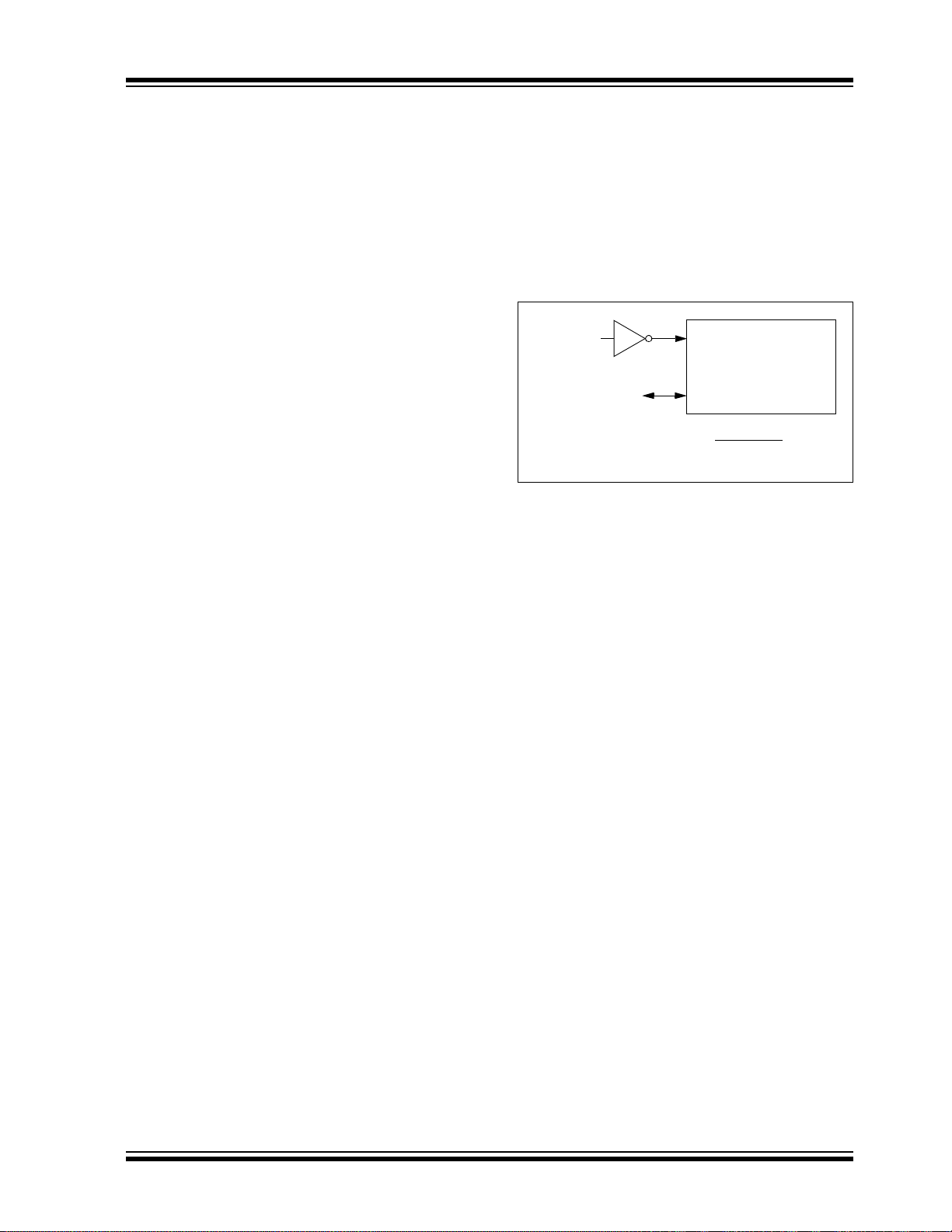
PIC16F/LF1946/47
OSC1/CLKIN
OSC2/CLKOUT
Clock from
Ext. System
PIC
®
MCU
FOSC/4 or
I/O
(1)
Note 1: Output depends upon CLKOUTEN bit of the
Configuration Word 1.
5.2 Clock Source Types
Clock sources can be classified as external or internal.
External clock sources rely on external circuitry for the
clock source to function. Examples are: oscillator modules (EC mode), quartz crystal resonators or ceramic
resonators (LP, XT and HS modes) and Resistor-Capacitor (RC) mode circuits.
Internal clock sources are contained internally within
the oscillator module. The internal oscillator block has
two internal oscillators and a dedicated
phase-locked-loop (HFPLL) that are used to generate
three internal system clock sources: the 16 MHz
High-Frequency Internal Oscillator (HFINTOSC), 500
kHZ (MFINTOSC) and the 31 kHz Low-Frequency
Internal Oscillator (LFINTOSC).
The system clock can be selected between external or
internal clock sources via the System Clock Select
(SCS) bits in the OSCCON register. See Section 5.3
“Clock Switching” for additional information.
5.2.1 EXTERNAL CLOCK SOURCES
An external clock source can be used as the device
system clock by performing one of the following
actions:
• Program the FOSC<2:0> bits in the Configuration
Word 1 to select an external clock source that will
be used as the default system clock upon a
device Reset.
• Write the SCS<1:0> bits in the OSCCON register
to switch the system clock source to:
- Timer1 Oscillator during run-time, or
- An external clock source determined by the
value of the FOSC bits.
See Section 5.3 “Clock Switching”for more information.
5.2.1.1 EC Mode
The External Clock (EC) mode allows an externally
generated logic level signal to be the system clock
source. When operating in this mode, an external clock
source is connected to the OSC1 input.
OSC2/CLKOUT is available for general purpose I/O or
CLKOUT. Figure 5-2 shows the pin connections for EC
mode.
EC mode has 3 power modes to select from through
Configuration Word 1:
• High-power, 4-32 MHz (FOSC = 111)
• Medium power, 0.5-4 MHz (FOSC = 110)
• Low-power, 0-0.5 MHz (FOSC = 101)
The Oscillator Start-up Timer (OST) is disabled when
EC mode is selected. Therefore, there is no delay in
operation after a Power-on Reset (POR) or wake-up
from Sleep. Because the PIC
®
MCU design is fully
static, stopping the external clock input will have the
effect of halting the device while leaving all data intact.
Upon restarting the external clock, the device will
resume operation as if no time had elapsed.
FIGURE 5-2: EXTERNAL CLOCK (EC)
MODE OPERATION
5.2.1.2 LP, XT, HS Modes
The LP, XT and HS modes support the use of quartz
crystal resonators or ceramic resonators connected to
OSC1 and OSC2 (Figure 5-3). The three modes select
a low, medium or high gain setting of the internal
inverter-amplifier to support various resonator types
and speed.
LP Oscillator mode selects the lowest gain setting of the
internal inverter-amplifier. LP mode current consumption
is the least of the three modes. This mode is designed to
drive only 32.768 kHz tuning-fork type crystals (watch
crystals).
XT Oscillator mode selects the intermediate gain
setting of the internal inverter-amplifier. XT mode
current consumption is the medium of the three modes.
This mode is best suited to drive resonators with a
medium drive level specification.
HS Oscillator mode selects the highest gain setting of the
internal inverter-amplifier. HS mode current consumption
is the highest of the three modes. This mode is best
suited for resonators that require a high drive setting.
Figure 5-3 and Figure 5-4 show typical circuits for
quartz crystal and ceramic resonators, respectively.
2010 Microchip Technology Inc. Preliminary DS41414B-page 63
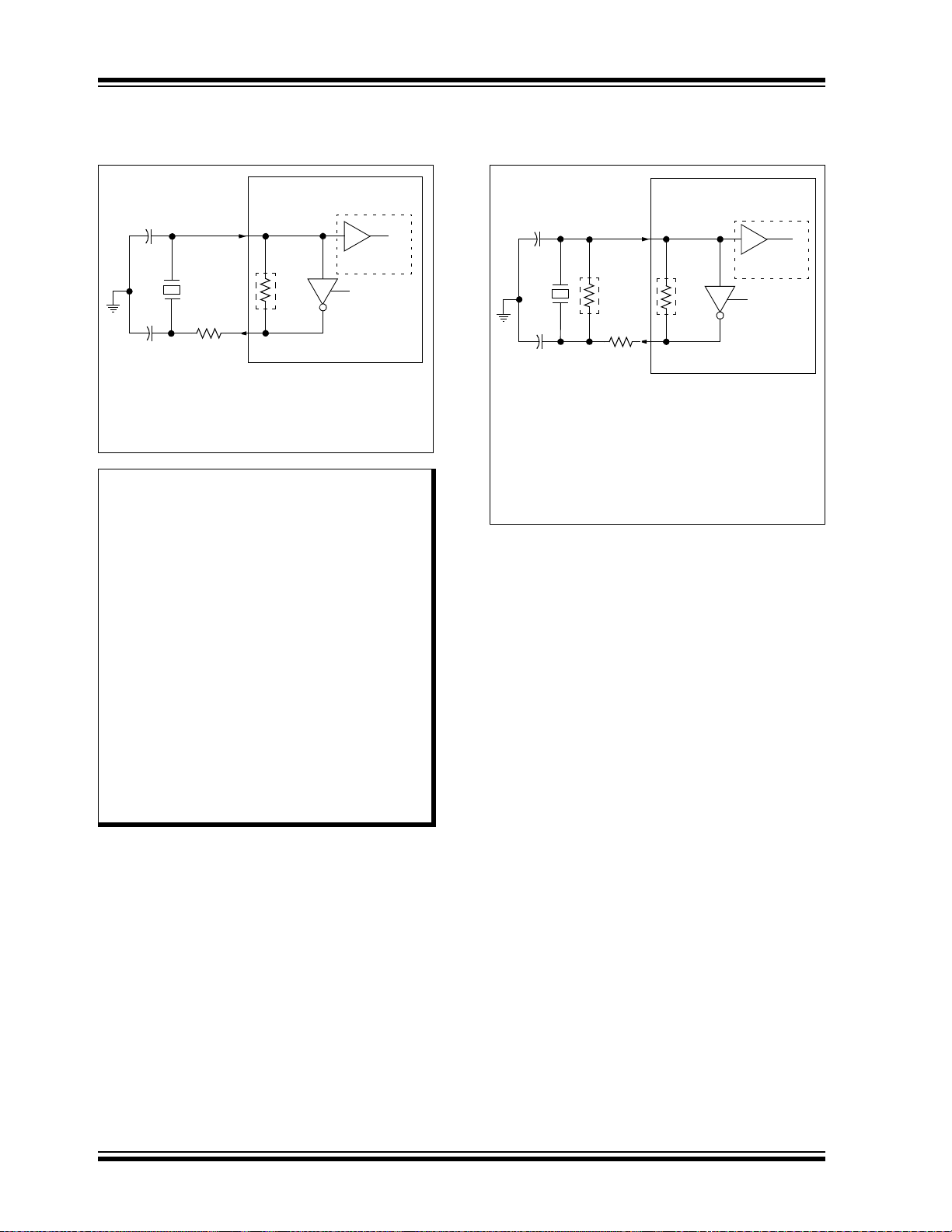
PIC16F/LF1946/47
Note 1: A series resistor (RS) may be required for
quartz crystals with low drive level.
2: The value of R
F varies with the Oscillator mode
selected (typically between 2 M to 10 M.
C1
C2
Quartz
R
S
(1)
OSC1/CLKIN
RF
(2)
Sleep
To Internal
Logic
PIC® MCU
Crystal
OSC2/CLKOUT
Note 1: A series resistor (RS) may be required for
ceramic resonators with low drive level.
2: The value of R
F varies with the Oscillator mode
selected (typically between 2 M to 10 M.
3: An additional parallel feedback resistor (R
P)
may be required for proper ceramic resonator
operation.
C1
C2
Ceramic
R
S
(1)
OSC1/CLKIN
RF
(2)
Sleep
To Internal
Logic
PIC® MCU
RP
(3)
Resonator
OSC2/CLKOUT
FIGURE 5-3: QUARTZ CRYSTAL
OPERATION (LP, XT OR
HS MODE)
Note 1: Quartz crystal characteristics vary
according to type, package and
manufacturer. The user should consult the
manufacturer data sheets for specifications
and recommended application.
2: Always verify oscillator performance over
DD and temperature range that is
the V
expected for the application.
3: For oscillator design assistance, reference
the following Microchip Applications Notes:
• AN826, “Crystal Oscillator Basics and
Crystal Selection for rfPIC
Devices” (DS00826)
• AN849, “Basic PIC
(DS00849)
• AN943, “Practical PIC
Analysis and Design” (DS00943)
• AN949, “Making Your Oscillator Work”
(DS00949)
®
and PIC
®
Oscillator Design”
®
Oscillator
FIGURE 5-4: CERAMIC RESONATOR
OPERATION
(XT OR HS MODE)
5.2.1.3 Oscillator Start-up Timer (OST)
If the oscillator module is configured for LP, XT or HS
modes, the Oscillator Start-up Timer (OST) counts
1024 oscillations from OSC1. This occurs following a
Power-on Reset (POR) and when the Power-up Timer
(PWRT) has expired (if configured), or a wake-up from
Sleep. During this time, the program counter does not
®
increment and program execution is suspended. The
OST ensures that the oscillator circuit, using a quartz
crystal resonator or ceramic resonator, has started and
is providing a stable system clock to the oscillator
module.
In order to minimize latency between external oscillator
start-up and code execution, the Two-Speed Clock
Start-up mode can be selected (see Section 5.4
“Two-Speed Clock Start-up Mode”).
DS41414B-page 64 Preliminary 2010 Microchip Technology Inc.
5.2.1.4 4X PLL
The oscillator module contains a 4X PLL that can be
used with both external and internal clock sources to
provide a system clock source. The input frequency for
the 4X PLL must fall within specifications. See the PLL
Clock Timing Specifications in Section 30.0
“Electrical Specifications”.
The 4X PLL may be enabled for use by one of two
methods:
1. Program the PLLEN bit in Configuration Word 2
to a ‘1’.
2. Write the SPLLEN bit in the OSCCON register to
a ‘1’. If the PLLEN bit in Configuration Word 2 is
programmed to a ‘1’, then the value of SPLLEN
is ignored.

PIC16F/LF1946/47
C1
C2
32.768 kHz
T1OSI
To Internal
Logic
PIC® MCU
Crystal
T1OSO
Quartz
OSC2/CLKOUT
CEXT
REXT
PIC® MCU
OSC1/CLKIN
F
OSC/4 or
Internal
Clock
VDD
VSS
Recommended values: 10 k REXT 100 k, <3V
3 k R
EXT 100 k, 3-5V
C
EXT > 20 pF, 2-5V
Note 1: Output depends upon CLKOUTEN bit of the
Configuration Word 1.
I/O
(1)
5.2.1.5 TIMER1 Oscillator
The Timer1 Oscillator is a separate crystal oscillator
that is associated with the Timer1 peripheral. It is optimized for timekeeping operations with a 32.768 kHz
crystal connected between the T1OSO and T1OSI
device pins.
The Timer1 Oscillator can be used as an alternate system clock source and can be selected during run-time
using clock switching. Refer to Section 5.3 “Clock
Switching” for more information.
FIGURE 5-5: QUARTZ CRYSTAL
OPERATION (TIMER1
OSCILLATOR)
5.2.1.6 External RC Mode
The external Resistor-Capacitor (RC) modes support
the use of an external RC circuit. This allows the
designer maximum flexibility in frequency choice while
keeping costs to a minimum when clock accuracy is not
required.
The RC circuit connects to OSC1. OSC2/CLKOUT is
available for general purpose I/O or CLKOUT. The
function of the OSC2/CLKOUT pin is determined by the
state of the CLKOUTEN
bit in Configuration Word 1.
Figure 5-6 shows the external RC mode connections.
FIGURE 5-6: EXTERNAL RC MODES
Note 1: Quartz crystal characteristics vary
according to type, package and
manufacturer. The user should consult the
manufacturer data sheets for specifications
and recommended application.
2: Always verify oscillator performance over
DD and temperature range that is
the V
expected for the application.
3: For oscillator design assistance, reference
the following Microchip Applications Notes:
• AN826, “Crystal Oscillator Basics and
Crystal Selection for rfPIC
Devices” (DS00826)
• AN849, “Basic PIC
(DS00849)
• AN943, “Practical PIC
2010 Microchip Technology Inc. Preliminary DS41414B-page 65
Analysis and Design” (DS00943)
• AN949, “Making Your Oscillator Work”
(DS00949)
• TB097, “Interfacing a Micro Crystal
MS1V-T1K 32.768 kHz Tuning Fork
Crystal to a PIC16F690/SS” (DS91097)
• AN1288, “Design Practices for
Low-Power External Oscillators”
(DS01288)
®
and PIC
®
Oscillator Design”
®
Oscillator
The RC oscillator frequency is a function of the supply
voltage, the resistor (R
EXT) and capacitor (CEXT) values
and the operating temperature. Other factors affecting
the oscillator frequency are:
• threshold voltage variation
• component tolerances
• packaging variations in capacitance
®
The user also needs to take into account variation due
to tolerance of external RC components used.

PIC16F/LF1946/47
5.2.2 INTERNAL CLOCK SOURCES
The device may be configured to use the internal oscillator block as the system clock by performing one of the
following actions:
• Program the FOSC<2:0> bits in Configuration
Word 1 to select the INTOSC clock source, which
will be used as the default system clock upon a
device Reset.
• Write the SCS<1:0> bits in the OSCCON register
to switch the system clock source to the internal
oscillator during run-time. See Section 5.3
“Clock Switching”for more information.
In INTOSC mode, OSC1/CLKIN is available for general
purpose I/O. OSC2/CLKOUT is available for general
purpose I/O or CLKOUT.
The function of the OSC2/CLKOUT pin is determined
by the state of the CLKOUTEN
Word 1.
The internal oscillator block has two independent
oscillators and a dedicated Phase-Locked Loop,
HFPLL that can produce one of three internal system
clock sources.
1. The HFINTOSC (High-Frequency Internal
Oscillator) is factory calibrated and operates at
16 MHz. The HFINTOSC source is generated
from the 500 kHz MFINTOSC source and the
dedicated Phase-Locked Loop, HFPLL. The
frequency of the HFINTOSC can be
user-adjusted via software using the OSCTUNE
register (Register 5-3).
2. The MFINTOSC (Medium-Frequency Internal
Oscillator) is factory calibrated and operates at
500 kHz. The frequency of the MFINTOSC can
be user-adjusted via software using the
OSCTUNE register (Register 5-3).
3. The LFINTOSC (Low-Frequency Internal
Oscillator) is uncalibrated and operates at
31 kHz.
bit in Configuration
5.2.2.1 HFINTOSC
The High-Frequency Internal Oscillator (HFINTOSC) is
a factory calibrated 16 MHz internal clock source. The
frequency of the HFINTOSC can be altered via
software using the OSCTUNE register (Register 5-3).
The output of the HFINTOSC connects to a postscaler
and multiplexer (see Figure 5-1). One of nine
frequencies derived from the HFINTOSC can be
selected via software using the IRCF<3:0> bits of the
OSCCON register. See Section5.2.2.7 “Internal
Oscillator Clock Switch Timing” for more information.
The HFINTOSC is enabled by:
• Configure the IRCF<3:0> bits of the OSCCON
register for the desired HF frequency, and
•FOSC<2:0> = 100, or
• Set the System Clock Source (SCS) bits of the
OSCCON register to ‘1x’.
The High Frequency Internal Oscillator Ready bit
(HFIOFR) of the OSCSTAT register indicates when the
HFINTOSC is running and can be utilized.
The High Frequency Internal Oscillator Status Locked
bit (HFIOFL) of the OSCSTAT register indicates when
the HFINTOSC is running within 2% of its final value.
The High Frequency Internal Oscillator Status Stable
bit (HFIOFS) of the OSCSTAT register indicates when
the HFINTOSC is running within 0.5% of its final value.
5.2.2.2 MFINTOSC
The Medium-Frequency Internal Oscillator
(MFINTOSC) is a factory calibrated 500 kHz internal
clock source. The frequency of the MFINTOSC can be
altered via software using the OSCTUNE register
(Register 5-3).
The output of the MFINTOSC connects to a postscaler
and multiplexer (see Figure 5-1). One of nine
frequencies derived from the MFINTOSC can be
selected via software using the IRCF<3:0> bits of the
OSCCON register. See Section5.2.2.7 “Internal
Oscillator Clock Switch Timing” for more information.
The MFINTOSC is enabled by:
• Configure the IRCF<3:0> bits of the OSCCON
register for the desired HF frequency, and
•FOSC<2:0> = 100, or
• Set the System Clock Source (SCS) bits of the
OSCCON register to ‘1x’
The Medium Frequency Internal Oscillator Ready bit
(MFIOFR) of the OSCSTAT register indicates when the
MFINTOSC is running and can be utilized.
DS41414B-page 66 Preliminary 2010 Microchip Technology Inc.

PIC16F/LF1946/47
5.2.2.3 Internal Oscillator Frequency
Adjustment
The 500 kHz internal oscillator is factory calibrated.
This internal oscillator can be adjusted in software by
writing to the OSCTUNE register (Register 5-3). Since
the HFINTOSC and MFINTOSC clock sources are
derived from the 500 kHz internal oscillator a change in
the OSCTUNE register value will apply to both.
The default value of the OSCTUNE register is ‘0’. The
value is a 6-bit two’s complement number. A value of
1Fh will provide an adjustment to the maximum
frequency. A value of 20h will provide an adjustment to
the minimum frequency.
When the OSCTUNE register is modified, the oscillator
frequency will begin shifting to the new frequency. Code
execution continues during this shift. There is no
indication that the shift has occurred.
OSCTUNE does not affect the LFINTOSC frequency.
Operation of features that depend on the LFINTOSC
clock source frequency, such as the Power-up Timer
(PWRT), Watchdog Timer (WDT), Fail-Safe Clock
Monitor (FSCM) and peripherals, are not affected by the
change in frequency.
5.2.2.4 LFINTOSC
The Low-Frequency Internal Oscillator (LFINTOSC) is
an uncalibrated 31 kHz internal clock source.
The output of the LFINTOSC connects to a postscaler
and multiplexer (see Figure 5-1). Select 31 kHz, via
software, using the IRCF<3:0> bits of the OSCCON
register. See Section 5.2.2.7 “Internal Oscillator
Clock Switch Timing” for more information. The
LFINTOSC is also the frequency for the Power-up Timer
(PWRT), Watchdog Timer (WDT) and Fail-Safe Clock
Monitor (FSCM).
The LFINTOSC is enabled by selecting 31 kHz
(IRCF<3:0> bits of the OSCCON register = 000) as the
system clock source (SCS bits of the OSCCON
register = 1x), or when any of the following are
enabled:
• Configure the IRCF<3:0> bits of the OSCCON
register for the desired LF frequency, and
•FOSC<2:0> = 100, or
• Set the System Clock Source (SCS) bits of the
OSCCON register to ‘1x’
Peripherals that use the LFINTOSC are:
• Power-up Timer (PWRT)
• Watchdog Timer (WDT)
• Fail-Safe Clock Monitor (FSCM)
The Low Frequency Internal Oscillator Ready bit
(LFIOFR) of the OSCSTAT register indicates when the
LFINTOSC is running and can be utilized.
5.2.2.5 Internal Oscillator Frequency
Selection
The system clock speed can be selected via software
using the Internal Oscillator Frequency Select bits
IRCF<3:0> of the OSCCON register.
The output of the 16 MHz HFINTOSC and 31 kHz
LFINTOSC connects to a postscaler and multiplexer
(see Figure 5-1). The Internal Oscillator Frequency
Select bits IRCF<3:0> of the OSCCON register select
the frequency output of the internal oscillators. One of
the following frequencies can be selected via software:
• 32 MHz (requires 4X PLL)
•16 MHz
•8 MHz
•4 MHz
•2 MHz
•1 MHz
• 500 kHz (Default after Reset)
•250 kHz
•125 kHz
•62.5 kHz
•31.25 kHz
• 31 kHz (LFINTOSC)
Note: Following any Reset, the IRCF<3:0> bits
of the OSCCON register are set to ‘0111’
and the frequency selection is set to
500 kHz. The user can modify the IRCF
bits to select a different frequency.
The IRCF<3:0> bits of the OSCCON register allow
duplicate selections for some frequencies. These duplicate choices can offer system design trade-offs. Lower
power consumption can be obtained when changing
oscillator sources for a given frequency. Faster transition times can be obtained between frequency changes
that use the same oscillator source.
2010 Microchip Technology Inc. Preliminary DS41414B-page 67

PIC16F/LF1946/47
5.2.2.6 32 MHz Internal Oscillator
Frequency Selection
The Internal Oscillator Block can be used with the 4X
PLL associated with the External Oscillator Block to
produce a 32 MHz internal system clock source. The
following settings are required to use the 32 MHz internal clock source:
• The FOSC bits in Configuration Word 1 must be
set to use the INTOSC source as the device system clock (FOSC<2:0> = 100).
• The SCS bits in the OSCCON register must be
cleared to use the clock determined by
FOSC<2:0> in Configuration Word 1
(SCS<1:0> = 00).
• The IRCF bits in the OSCCON register must be
set to the 8 MHz HFINTOSC set to use
(IRCF<3:0> = 1110).
• The SPLLEN bit in the OSCCON register must be
set to enable the 4xPLL, or the PLLEN bit of the
Configuration Word 2 must be programmed to a
‘1’.
Note: When using the PLLEN bit of the
Configuration Word 2, the 4xPLL cannot
be disabled by software and the 8 MHz
HFINTOSC option will no longer be
available.
The 4xPLL is not available for use with the internal
oscillator when the SCS bits of the OSCCON register
are set to ‘1x’. The SCS bits must be set to ‘00’ to use
the 4xPLL with the internal oscillator.
5.2.2.7 Internal Oscillator Clock Switch
Timing
When switching between the HFINTOSC, MFINTOSC
and the LFINTOSC, the new oscillator may already be
shut down to save power (see Figure 5-7). If this is the
case, there is a delay after the IRCF<3:0> bits of the
OSCCON register are modified before the frequency
selection takes place. The OSCSTAT register will
reflect the current active status of the HFINTOSC,
MFINTOSC and LFINTOSC oscillators. The sequence
of a frequency selection is as follows:
1. IRCF<3:0> bits of the OSCCON register are
modified.
2. If the new clock is shut down, a clock start-up
delay is started.
3. Clock switch circuitry waits for a falling edge of
the current clock.
4. The current clock is held low and the clock
switch circuitry waits for a rising edge in the new
clock.
5. The new clock is now active.
6. The OSCSTAT register is updated as required.
7. Clock switch is complete.
See Figure 5-7 for more details.
If the internal oscillator speed is switched between two
clocks of the same source, there is no start-up delay
before the new frequency is selected. Clock switching
time delays are shown in Table 5-1.
Start-up delay specifications are located in the
oscillator tables of Section 30.0 “Electrical
Specifications”
DS41414B-page 68 Preliminary 2010 Microchip Technology Inc.
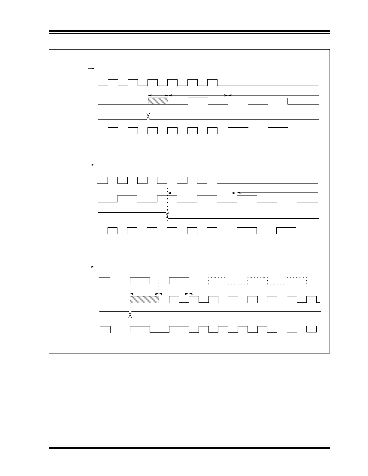
FIGURE 5-7: INTERNAL OSCILLATOR SWITCH TIMING
HFINTOSC/
LFINTOSC
IRCF <3:0>
System Clock
HFINTOSC/
LFINTOSC
IRCF <3:0>
System Clock
0 0
0 0
Start-up Time
2-cycle Sync Running
2-cycle Sync Running
HFINTOSC/ LFINTOSC (FSCM and WDT disabled)
HFINTOSC/
LFINTOSC (Either FSCM or WDT enabled)
LFINTOSC
HFINTOSC/
IRCF <3:0>
System Clock
= 0 0
Start-up Time 2-cycle Sync
Running
LFINTOSC HFINTOSC/MFINTOSC
LFINTOSC turns off unless WDT or FSCM is enabled
MFINTOSC
MFINTOSC
MFINTOSC
MFINTOSC
MFINTOSC
PIC16F/LF1946/47
2010 Microchip Technology Inc. Preliminary DS41414B-page 69

PIC16F/LF1946/47
5.3 Clock Switching
The system clock source can be switched between
external and internal clock sources via software using
the System Clock Select (SCS) bits of the OSCCON
register. The following clock sources can be selected
using the SCS bits:
• Default system oscillator determined by FOSC
bits in Configuration Word 1
• Timer1 32 kHz crystal oscillator
• Internal Oscillator Block (INTOSC)
5.3.1 SYSTEM CLOCK SELECT (SCS)
BITS
The System Clock Select (SCS) bits of the OSCCON
register selects the system clock source that is used for
the CPU and peripherals.
• When the SCS bits of the OSCCON register = 00,
the system clock source is determined by value of
the FOSC<2:0> bits in the Configuration Word 1.
• When the SCS bits of the OSCCON register = 01,
the system clock source is the Timer1 oscillator.
• When the SCS bits of the OSCCON register = 1x,
the system clock source is chosen by the internal
oscillator frequency selected by the IRCF<3:0>
bits of the OSCCON register. After a Reset, the
SCS bits of the OSCCON register are always
cleared.
Note: Any automatic clock switch, which may
occur from Two-Speed Start-up or
Fail-Safe Clock Monitor, does not update
the SCS bits of the OSCCON register. The
user can monitor the OSTS bit of the
OSCSTAT register to determine the current
system clock source.
5.3.3 TIMER1 OSCILLATOR
The Timer1 Oscillator is a separate crystal oscillator
associated with the Timer1 peripheral. It is optimized
for timekeeping operations with a 32.768 kHz crystal
connected between the T1OSO and T1OSI device
pins.
The Timer1 oscillator is enabled using the T1OSCEN
control bit in the T1CON register. See Section 21.0
“Timer1 Module with Gate Control” for more
information about the Timer1 peripheral.
5.3.4 TIMER1 OSCILLATOR READY
(T1OSCR) BIT
The user must ensure that the Timer1 Oscillator is
ready to be used before it is selected as a system clock
source. The Timer1 Oscillator Ready (T1OSCR) bit of
the OSCSTAT register indicates whether the Timer1
oscillator is ready to be used. After the T1OSCR bit is
set, the SCS bits can be configured to select the Timer1
oscillator.
When switching between clock sources, a delay is
required to allow the new clock to stabilize. These oscillator delays are shown in Table 5-1.
5.3.2 OSCILLATOR START-UP TIME-OUT
STATUS (OSTS) BIT
The Oscillator Start-up Time-out Status (OSTS) bit of
the OSCSTAT register indicates whether the system
clock is running from the external clock source, as
defined by the FOSC<2:0> bits in the Configuration
Word 1, or from the internal clock source. In particular,
OSTS indicates that the Oscillator Start-up Timer
(OST) has timed out for LP, XT or HS modes. The OST
does not reflect the status of the Timer1 Oscillator.
DS41414B-page 70 Preliminary 2010 Microchip Technology Inc.

PIC16F/LF1946/47
5.4 Two-Speed Clock Start-up Mode
Two-Speed Start-up mode provides additional power
savings by minimizing the latency between external
oscillator start-up and code execution. In applications
that make heavy use of the Sleep mode, Two-Speed
Start-up will remove the external oscillator start-up
time from the time spent awake and can reduce the
overall power consumption of the device. This mode
allows the application to wake-up from Sleep, perform
a few instructions using the INTOSC internal oscillator
block as the clock source and go back to Sleep without
waiting for the external oscillator to become stable.
Two-Speed Start-up provides benefits when the oscillator module is configured for LP, XT, or HS modes.
The Oscillator Start-up Timer (OST) is enabled for
these modes and must count 1024 oscillations before
the oscillator can be used as the system clock source.
If the oscillator module is configured for any mode
other than LP, XT or HS mode, then Two-Speed
Start-up is disabled. This is because the external clock
oscillator does not require any stabilization time after
POR or an exit from Sleep.
If the OST count reaches 1024 before the device
enters Sleep mode, the OSTS bit of the OSCSTAT register is set and program execution switches to the
external oscillator. However, the system may never
operate from the external oscillator if the time spent
awake is very short.
Note: Executing a SLEEP instruction will abort
the oscillator start-up time and will cause
the OSTS bit of the OSCSTAT register to
remain clear.
5.4.1 TWO-SPEED START-UP MODE CONFIGURATION
Two-Speed Start-up mode is configured by the
following settings:
• IESO (of the Configuration Word 1) = 1; Inter-
nal/External Switchover bit (Two-Speed Start-up
mode enabled).
• SCS (of the OSCCON register) = 00.
• FOSC<2:0> bits in the Configuration Word 1
configured for LP, XT or HS mode.
Two-Speed Start-up mode is entered after:
• Power-on Reset (POR) and, if enabled, after
Power-up Timer (PWRT) has expired, or
• Wake-up from Sleep.
TABLE 5-1: OSCILLATOR SWITCHING DELAYS
Switch From Switch To Frequency Oscillator Delay
(1)
(1)
(1)
(1)
(1)
(1)
(1)
(1)
(1)
31 kHz
31.25 kHz-500 kHz
Oscillator Warm-up Delay (T
31.25kHz-16MHz
DC – 32 MHz 2 cycles
DC – 32 MHz 1 cycle of each
32 kHz-20 MHz 1024 Clock Cycles (OST)
31.25 kHz-500 kHz
31.25kHz-16MHz
2 s (approx.)
31 kHz 1 cycle of each
WARM)
LFINTOSC
Sleep/POR
MFINTOSC
HFINTOSC
Sleep/POR EC, RC
LFINTOSC EC, RC
Sleep/POR
Any clock source
Timer1 Oscillator
LP, XT, HS
MFINTOSC
HFINTOSC
Any clock source LFINTOSC
Any clock source Timer1 Oscillator 32 kHz 1024 Clock Cycles (OST)
PLL inactive PLL active 16-32 MHz 2 ms (approx.)
Note 1: PLL inactive.
2010 Microchip Technology Inc. Preliminary DS41414B-page 71

PIC16F/LF1946/47
0 1 1022 1023
PC + 1
TOSTT
INTOSC
OSC1
OSC2
Program Counter
System Clock
PC - N
PC
5.4.2 TWO-SPEED START-UP SEQUENCE
1. Wake-up from Power-on Reset or Sleep.
2. Instructions begin execution by the internal
oscillator at the frequency set in the IRCF<3:0>
bits of the OSCCON register.
3. OST enabled to count 1024 clock cycles.
4. OST timed out, wait for falling edge of the
internal oscillator.
5. OSTS is set.
6. System clock held low until the next falling edge
of new clock (LP, XT or HS mode).
7. System clock is switched to external clock
source.
FIGURE 5-8: TWO-SPEED START-UP
5.4.3 CHECKING TWO-SPEED CLOCK STATUS
Checking the state of the OSTS bit of the OSCSTAT
register will confirm if the microcontroller is running
from the external clock source, as defined by the
FOSC<2:0> bits in the Configuration Word 1, or the
internal oscillator.
DS41414B-page 72 Preliminary 2010 Microchip Technology Inc.

PIC16F/LF1946/47
External
LFINTOSC
÷ 64
S
R
Q
31 kHz
(~32 s)
488 Hz
(~2 ms)
Clock Monitor
Latch
Clock
Failure
Detected
Oscillator
Clock
Q
Sample Clock
5.5 Fail-Safe Clock Monitor
The Fail-Safe Clock Monitor (FSCM) allows the device
to continue operating should the external oscillator fail.
The FSCM can detect oscillator failure any time after
the Oscillator Start-up Timer (OST) has expired. The
FSCM is enabled by setting the FCMEN bit in the
Configuration Word 1. The FSCM is applicable to all
external Oscillator modes (LP, XT, HS, EC, Timer1
Oscillator and RC).
FIGURE 5-9: FSCM BLOCK DIAGRAM
5.5.1 FAIL-SAFE DETECTION
The FSCM module detects a failed oscillator by
comparing the external oscillator to the FSCM sample
clock. The sample clock is generated by dividing the
LFINTOSC by 64. See Figure 5-9. Inside the fail
detector block is a latch. The external clock sets the
latch on each falling edge of the external clock. The
sample clock clears the latch on each rising edge of the
sample clock. A failure is detected when an entire
half-cycle of the sample clock elapses before the
external clock goes low.
5.5.3 FAIL-SAFE CONDITION CLEARING
The Fail-Safe condition is cleared after a Reset,
executing a SLEEP instruction or changing the SCS bits
of the OSCCON register. When the SCS bits are
changed, the OST is restarted. While the OST is
running, the device continues to operate from the
INTOSC selected in OSCCON. When the OST times
out, the Fail-Safe condition is cleared and the device
will be operating from the external clock source. The
Fail-Safe condition must be cleared before the OSFIF
flag can be cleared.
5.5.4 RESET OR WAKE-UP FROM SLEEP
The FSCM is designed to detect an oscillator failure
after the Oscillator Start-up Timer (OST) has expired.
The OST is used after waking up from Sleep and after
any type of Reset. The OST is not used with the EC or
RC Clock modes so that the FSCM will be active as
soon as the Reset or wake-up has completed. When
the FSCM is enabled, the Two-Speed Start-up is also
enabled. Therefore, the device will always be executing
code while the OST is operating.
Note: Due to the wide range of oscillator start-up
times, the Fail-Safe circuit is not active
during oscillator start-up (i.e., after exiting
Reset or Sleep). After an appropriate
amount of time, the user should check the
Status bits in the OSCSTAT register to
verify the oscillator start-up and that the
system clock switchover has successfully
completed.
5.5.2 FAIL-SAFE OPERATION
When the external clock fails, the FSCM switches the
device clock to an internal clock source and sets the bit
flag OSFIF of the PIR2 register. Setting this flag will
generate an interrupt if the OSFIE bit of the PIE2
register is also set. The device firmware can then take
steps to mitigate the problems that may arise from a
failed clock. The system clock will continue to be
sourced from the internal clock source until the device
firmware successfully restarts the external oscillator
and switches back to external operation.
The internal clock source chosen by the FSCM is
determined by the IRCF<3:0> bits of the OSCCON
register. This allows the internal oscillator to be
configured before a failure occurs.
2010 Microchip Technology Inc. Preliminary DS41414B-page 73

PIC16F/LF1946/47
OSCFIF
System
Clock
Output
Sample Clock
Failure
Detected
Oscillator
Failure
Note: The system clock is normally at a much higher frequency than the sample clock. The relative frequencies in
this example have been chosen for clarity.
(Q)
Te st
Test Test
Clock Monitor Output
FIGURE 5-10: FSCM TIMING DIAGRAM
DS41414B-page 74 Preliminary 2010 Microchip Technology Inc.

PIC16F/LF1946/47
5.6 Oscillator Control Registers
REGISTER 5-1: OSCCON: OSCILLATOR CONTROL REGISTER
R/W-0/0 R/W-0/0 R/W-1/1 R/W-1/1 R/W-1/1 U-0 R/W-0/0 R/W-0/0
SPLLEN IRCF<3:0>
bit 7 bit 0
Legend:
R = Readable bit W = Writable bit U = Unimplemented bit, read as ‘0’
u = Bit is unchanged x = Bit is unknown -n/n = Value at POR and BOR/Value at all other Resets
‘1’ = Bit is set ‘0’ = Bit is cleared
bit 7 SPLLEN: Software PLL Enable bit
If PLLEN in Configuration Word 1 =
SPLLEN bit is ignored. 4x PLL is always enabled (subject to oscillator requirements)
If PLLEN in Configuration Word 1 = 0:
1 = 4x PLL Is enabled
0 = 4x PLL is disabled
bit 6-3 IRCF<3:0>: Internal Oscillator Frequency Select bits
000x =31 kHz LF
0010 =31.25 kHz MF
0011 =31.25 kHz HF
0100 =62.5 kHz MF
0101 =125 kHz MF
0110 =250 kHz MF
0111 =500 kHz MF (default upon Reset)
1000 =125 kHz HF
1001 =250 kHz HF
1010 =500 kHz HF
1011 =1 MHz HF
1100 =2 MHz HF
1101 =4 MHz HF
1110 =8 MHz or 32 MHz HF(see Section 5.2.2.1 “HFINTOSC”)
1111 =16 MHz HF
bit 2 Unimplemented: Read as ‘0’
bit 1-0 SCS<1:0>: System Clock Select bits
1x = Internal oscillator block
01 = Timer1 oscillator
00 = Clock determined by FOSC<2:0> in Configuration Word 1.
(1)
(1)
(1)
(1)
1:
—
SCS<1:0>
Note 1: Duplicate frequency derived from HFINTOSC.
2010 Microchip Technology Inc. Preliminary DS41414B-page 75

PIC16F/LF1946/47
REGISTER 5-2: OSCSTAT: OSCILLATOR STATUS REGISTER
R-1/q R-0/q R-q/q R-0/q R-0/q R-q/q R-0/0 R-0/q
T1OSCR PLLR OSTS HFIOFR HFIOFL MFIOFR LFIOFR HFIOFS
bit 7 bit 0
Legend:
R = Readable bit W = Writable bit U = Unimplemented bit, read as ‘0’
u = Bit is unchanged x = Bit is unknown -n/n = Value at POR and BOR/Value at all other Resets
‘1’ = Bit is set ‘0’ = Bit is cleared q = Conditional
bit 7 T1OSCR: Timer1 Oscillator Ready bit
If T1OSCEN =
1 = Timer1 oscillator is ready
0 = Timer1 oscillator is not ready
If T1OSCEN = 0
1 = Timer1 clock source is always ready
bit 6 PLLR 4x PLL Ready bit
1 = 4x PLL is ready
0 = 4x PLL is not ready
bit 5 OSTS: Oscillator Start-up Time-out Status bit
1 = Running from the clock defined by the FOSC<2:0> bits of the Configuration Word 1
0 = Running from an internal oscillator
bit 4 HFIOFR: High Frequency Internal Oscillator Ready bit
1 = HFINTOSC is ready
0 = HFINTOSC is not ready
bit 3 HFIOFL: High Frequency Internal Oscillator Locked bit
1 = HFINTOSC is at least 2% accurate
0 = HFINTOSC is not 2% accurate
bit 2 MFIOFR: Medium Frequency Internal Oscillator Ready bit
1 = MFINTOSC is ready
0 = MFINTOSC is not ready
bit 1 LFIOFR: Low Frequency Internal Oscillator Ready bit
1 = LFINTOSC is ready
0 = LFINTOSC is not ready
bit 0 HFIOFS: High Frequency Internal Oscillator Stable bit
1 = HFINTOSC is at least 0.5% accurate
0 = HFINTOSC is not 0.5% accurate
1:
:
DS41414B-page 76 Preliminary 2010 Microchip Technology Inc.

PIC16F/LF1946/47
REGISTER 5-3: OSCTUNE: OSCILLATOR TUNING REGISTER
U-0 U-0 R/W-0/0 R/W-0/0 R/W-0/0 R/W-0/0 R/W-0/0 R/W-0/0
— — TUN<5:0>
bit 7 bit 0
Legend:
R = Readable bit W = Writable bit U = Unimplemented bit, read as ‘0’
u = Bit is unchanged x = Bit is unknown -n/n = Value at POR and BOR/Value at all other Resets
‘1’ = Bit is set ‘0’ = Bit is cleared
bit 7-6 Unimplemented: Read as ‘0’
bit 5-0 TUN<4:0>: Frequency Tuning bits
011111 = Maximum frequency
011110 =
•
•
•
000001 =
000000 = Oscillator module is running at the factory-calibrated frequency.
111111 =
•
•
•
100000 = Minimum frequency
TABLE 5-2: SUMMARY OF REGISTERS ASSOCIATED WITH CLOCK SOURCES
Name Bit 7 Bit 6 Bit 5 Bit 4 Bit 3 Bit 2 Bit 1 Bit 0
OSCCON SPLLEN IRCF<3:0>
OSCSTAT T1OSCR PLLR OSTS HFIOFR HFIOFL MFIOFR LFIOFR HFIOFS 76
OSCTUNE
PIE2 OSFIE
PIR2
T1CON
Legend: — = unimplemented location, read as ‘0’. Shaded cells are not used by clock sources.
Note 1: PIC16F1947 only.
— —TUN<5:0>77
C2IE C1IE EEIE BCLIE
OSFIF
TMR1CS<1:0> T1CKPS<1:0> T1OSCEN T1SYNC — TMR1ON
C2IF C1IF EEIF BCLIF LCDIF C3IF CCP2IF
—SCS<1:0>75
LCDIE
C3IE CCP2IE
Register
on Page
(1)
(1)
TABLE 5-3: SUMMARY OF CONFIGURATION WORD WITH CLOCK SOURCES
Name Bits Bit -/7 Bit -/6 Bit 13/5 Bit 12/4 Bit 11/3 Bit 10/2 Bit 9/1 Bit 8/0
CONFIG1
CONFIG2
Legend: — = unimplemented location, read as ‘0’. Shaded cells are not used by clock sources.
Note 1: PIC16F1946/47 only.
13:8
7:0
13:8
7:0
— — FCMEN IESO CLKOUTEN BOREN<1:0> CPD
CP MCLRE PWRTE WDTE<1:0> FOSC<2:0>
— — LVP DEBUG — BORV STVREN PLLEN
— — —VCAPEN— — WRT<1:0>
Register
on Page
95
99
205
56
58
2010 Microchip Technology Inc. Preliminary DS41414B-page 77

PIC16F/LF1946/47
NOTES:
DS41414B-page 78 Preliminary 2010 Microchip Technology Inc.

PIC16F/LF1946/47
External Reset
MCLR
VDD
WDT
Time-out
Power-on
Reset
LFINTOSC
PWRT
64 ms
PWRTEN
Brown-out
Reset
BOR
RESET Instruction
Stack
Pointer
Stack Overflow/Underflow Reset
Sleep
MCLRE
Enable
Device
Reset
Zero
Programming Mode Exit
6.0 RESETS
There are multiple ways to reset this device:
• Power-on Reset (POR)
• Brown-out Reset (BOR)
•MCLR
•WDT Reset
• RESET instruction
• Stack Overflow
• Stack Underflow
• Programming mode exit
To a ll o w V
can be enabled to extend the Reset time after a BOR
or POR event.
A simplified block diagram of the On-Chip Reset Circuit
is shown in Figure 6-1.
FIGURE 6-1: SIMPLIFIED BLOCK DIAGRAM OF ON-CHIP RESET CIRCUIT
Reset
DD to stabilize, an optional power-up timer
2010 Microchip Technology Inc. Preliminary DS41414B-page 79

PIC16F/LF1946/47
6.1 Power-on Reset (POR)
The POR circuit holds the device in Reset until VDD has
reached an acceptable level for minimum operation.
Slow rising V
performance may require greater than minimum V
The PWRT, BOR or MCLR
extend the start-up period until all device operation
conditions have been met.
6.1.1 POWER-UP TIMER (PWRT)
The Power-up Timer provides a nominal 64 ms timeout on POR or Brown-out Reset.
The device is held in Reset as long as PWRT is active.
The PWRT delay allows additional time for the V
rise to an acceptable level. The Power-up Timer is
enabled by clearing the PWRTE bit in Configuration
Word 1.
The Power-up Timer starts after the release of the POR
and BOR.
For additional information, refer to Application Note
AN607, “Power-up Trouble Shooting” (DS00607).
DD, fast operating speeds or analog
DD.
features can be used to
DD to
6.2 Brown-Out Reset (BOR)
The BOR circuit holds the device in Reset when Vdd
reaches a selectable minimum level. Between the
POR and BOR, complete voltage range coverage for
execution protection can be implemented.
The Brown-out Reset module has four operating
modes controlled by the BOREN<1:0> bits in Configuration Word 1. The four operating modes are:
• BOR is always on
• BOR is off when in Sleep
• BOR is controlled by software
• BOR is always off
Refer to Tab le 6- 1 for more information.
The Brown-out Reset voltage level is selectable by
configuring the BORV bit in Configuration Word 2.
DD noise rejection filter prevents the BOR from trig-
A V
gering on small events. If V
duration greater than parameter T
will reset. See Figure 6-3 for more information.
DD falls below VBOR for a
BORDC, the device
TABLE 6-1: BOR OPERATING MODES
BOREN
Config bits
BOR_ON (11) X X Active Waits for BOR ready
SBOREN Device Mode BOR Mode
Device
Operation upon
release of POR
Device
Operation upon
wake-up from
Sleep
(1)
BOR_NSLEEP (10) X Awake Active
BOR_NSLEEP (10) X Sleep Disabled
BOR_SBOREN (01) 1 X Active Begins immediately
BOR_SBOREN (01) 0 X Disabled Begins immediately
BOR_OFF (00) X X Disabled Begins immediately
Note 1: Even though this case specifically waits for the BOR, the BOR is already operating, so there is no delay in
start-up.
6.2.1 BOR IS ALWAYS ON
When the BOREN bits of Configuration Word 1 are set
to ‘11’, the BOR is always on. The device start-up will
be delayed until the BOR is ready and VDD is higher
than the BOR threshold.
BOR protection is active during Sleep. The BOR does
not delay wake-up from Sleep.
6.2.2 BOR IS OFF IN SLEEP
When the BOREN bits of Configuration Word 1 are set
to ‘10’, the BOR is on, except in Sleep. The device
start-up will be delayed until the BOR is ready and V
is higher than the BOR threshold.
BOR protection is not active during Sleep. The device
wake-up will be delayed until the BOR is ready.
DD
6.2.3 BOR CONTROLLED BY SOFTWARE
When the BOREN bits of Configuration Word 1 are set
to ‘01’, the BOR is controlled by the SBOREN bit of the
BORCON register. The device start-up is not delayed
by the BOR ready condition or the V
BOR protection begins as soon as the BOR circuit is
ready. The status of the BOR circuit is reflected in the
BORRDY bit of the BORCON register.
BOR protection is unchanged by Sleep.
Waits for BOR ready
DD level.
DS41414B-page 80 Preliminary 2010 Microchip Technology Inc.

FIGURE 6-2: BROWN-OUT READY
TBORRDY
SBOREN
BORRDY
BOR Protection Active
TPWRT
(1)
VBOR
V
DD
Internal
Reset
VBOR
V
DD
Internal
Reset
TPWRT
(1)
< TPWRT
TPWRT
(1)
VBOR
V
DD
Internal
Reset
Note 1: TPWRT delay only if PWRTE bit is programmed to ‘0’.
FIGURE 6-3: BROWN-OUT SITUATIONS
PIC16F/LF1946/47
REGISTER 6-1: BORCON: BROWN-OUT RESET CONTROL REGISTER
R/W-1/u U-0 U-0 U-0 U-0 U-0 U-0 R-q/u
SBOREN
bit 7 bit 0
Legend:
R = Readable bit W = Writable bit U = Unimplemented bit, read as ‘0’
u = Bit is unchanged x = Bit is unknown -n/n = Value at POR and BOR/Value at all other Resets
‘1’ = Bit is set ‘0’ = Bit is cleared q = Value depends on condition
bit 7 SBOREN: Software Brown-out Reset Enable bit
bit 6-1 Unimplemented: Read as ‘0’
bit 0 BORRDY: Brown-out Reset Circuit Ready Status bit
2010 Microchip Technology Inc. Preliminary DS41414B-page 81
— — — — — —BORRDY
If BOREN <1:0> in Configuration Word 1
SBOREN is read/write, but has no effect on the BOR.
If BOREN <1:0> in Configuration Word 1 =
1 = BOR Enabled
0 = BOR Disabled
1 = The Brown-out Reset circuit is active
0 = The Brown-out Reset circuit is inactive
01:
01:

PIC16F/LF1946/47
6.3 MCLR
The MCLR is an optional external input that can reset
the device. The MCLR
MCLRE bit of Configuration Word 1 and the LVP bit of
Configuration Word 2 (Ta b le 6 -2 ).
function is controlled by the
TABLE 6-2: MCLR CONFIGURATION
MCLRE LVP MCLR
00Disabled
10Enabled
x1Enabled
6.3.1 MCLR ENABLED
When MCLR is enabled and the pin is held low, the
device is held in Reset. The MCLR
DD through an internal weak pull-up.
V
The device has a noise filter in the MCLR
The filter will detect and ignore small pulses.
Note: A Reset does not drive the MCLR pin low.
pin is connected to
Reset path.
6.3.2 MCLR DISABLED
When MCLR is disabled, the pin functions as a general
purpose input and the internal weak pull-up is under
software control. See Section 12.6 “PORTE
Registers” for more information.
6.4 Watchdog Timer (WDT) Reset
The Watchdog Timer generates a Reset if the firmware
does not issue a CLRWDT instruction within the time-out
period. The TO and PD bits in the STATUS register are
changed to indicate the WDT Reset. See Section 10.0
“Watchdog Timer” for more information.
6.7 Programming Mode Exit
Upon exit of Programming mode, the device will
behave as if a POR had just occurred.
6.8 Power-Up Timer
The Power-up Timer optionally delays device execution
after a BOR or POR event. This timer is typically used to
allow VDD to stabilize before allowing the device to start
running.
The Power-up Timer is controlled by the PWRTE
Configuration Word 1.
bit of
6.9 Start-up Sequence
Upon the release of a POR or BOR, the following must
occur before the device will begin executing:
1. Power-up Timer runs to completion (if enabled).
2. Oscillator start-up timer runs to completion (if
required for oscillator source).
3. MCLR
The total time-out will vary based on oscillator configuration and Power-up Timer configuration. See
Section 5.0 “Oscillator Module (With Fail-Safe
Clock Monitor)” for more information.
The Power-up Timer and oscillator start-up timer run
independently of MCLR
enough, the Power-up Timer and oscillator start-up
timer will expire. Upon bringing MCLR
will begin execution immediately (see Figure 6-4). This
is useful for testing purposes or to synchronize more
than one device operating in parallel.
must be released (if enabled).
Reset. If MCLR is kept low long
high, the device
6.5 RESET Instruction
A RESET instruction will cause a device Reset. The RI
bit in the PCON register will be set to ‘0’. See Ta b le 6- 4
for default conditions after a RESET instruction has
occurred.
6.6 Stack Overflow/Underflow Reset
The device can reset when the Stack Overflows or
Underflows. The STKOVF or STKUNF bits of the PCON
register indicate the Reset condition. These Resets are
enabled by setting the STVREN bit in Configuration Word
2. See Section 3 .4.2 “Overflow/Underflow Reset” for
more information.
DS41414B-page 82 Preliminary 2010 Microchip Technology Inc.

FIGURE 6-4: RESET START-UP SEQUENCE
TOST
TMCLR
TPWRT
VDD
Internal POR
Power Up Timer
MCLR
Internal RESET
Oscillator Modes
Oscillator Start Up Timer
Oscillator
F
OSC
Internal Oscillator
Oscillator
F
OSC
External Clock (EC)
CLKIN
F
OSC
External Crystal
PIC16F/LF1946/47
2010 Microchip Technology Inc. Preliminary DS41414B-page 83

PIC16F/LF1946/47
6.10 Determining the Cause of a Reset
Upon any Reset, multiple bits in the STATUS and
PCON register are updated to indicate the cause of the
Reset. Ta bl e 6 -3 and Tab le 6 -4 show the Reset
conditions of these registers.
TABLE 6-3: RESET STATUS BITS AND THEIR SIGNIFICANCE
STKOVF STKUNF RMCLR RI POR BOR TO PD Condition
00110x11Power-on Reset
00110x0xIllegal, TO
00110xx0Illegal, PD is set on POR
0011u011Brown-out Reset
uuuuuu0uWDT Reset
uuuuuu00WDT Wake-up from Sleep
uuuuuu10Interrupt Wake-up from Sleep
uu0uuuuuMCLR
uu0uuu10MCLR
u u u 0 u u u u RESET Instruction Executed
1uuuuuuuStack Overflow Reset (STVREN = 1)
u1uuuuuuStack Underflow Reset (STVREN = 1)
is set on POR
Reset during normal operation
Reset during Sleep
(1)
(2)
STATUS
Register
---1 0uuu uu-- uuuu
PCON
Register
TABLE 6-4: RESET CONDITION FOR SPECIAL REGISTERS
Condition
Power-on Reset 0000h ---1 1000 00-- 110x
MCLR
Reset during normal operation 0000h ---u uuuu uu-- 0uuu
MCLR Reset during Sleep 0000h ---1 0uuu uu-- 0uuu
WDT Reset 0000h ---0 uuuu uu-- uuuu
WDT Wake-up from Sleep PC + 1 ---0 0uuu uu-- uuuu
Brown-out Reset 0000h ---1 1uuu 00-- 11u0
Interrupt Wake-up from Sleep PC + 1
RESET Instruction Executed 0000h ---u uuuu uu-- u0uu
Stack Overflow Reset (STVREN = 1) 0000h ---u uuuu 1u-- uuuu
Stack Underflow Reset (STVREN = 1) 0000h ---u uuuu u1-- uuuu
Legend: u = unchanged, x = unknown, - = unimplemented bit, reads as ‘0’.
Note1: When the wake-up is due to an interrupt and Global Enable bit (GIE) is set, the return address is pushed on
the stack and PC is loaded with the interrupt vector (0004h) after execution of PC + 1.
2: If a Status bit is not implemented, that bit will be read as ‘0’.
Program
Counter
DS41414B-page 84 Preliminary 2010 Microchip Technology Inc.

PIC16F/LF1946/47
6.11 Power Control (PCON) Register
The Power Control (PCON) register contains flag bits
to differentiate between a:
• Power-on Reset (POR
• Brown-out Reset (BOR)
• Reset Instruction Reset (RI
• Stack Overflow Reset (STKOVF)
• Stack Underflow Reset (STKUNF)
•MCLR
The PCON register bits are shown in Register 6-2.
Reset (RMCLR)
REGISTER 6-2: PCON: POWER CONTROL REGISTER
R/W/HS-0/q R/W/HS-0/q U-0 U-0 R/W/HC-1/q R/W/HC-1/q R/W/HC-q/u R/W/HC-q/u
STKOVF STKUNF
bit 7 bit 0
Legend:
HC = Bit is cleared by hardware HS = Bit is set by hardware
R = Readable bit W = Writable bit U = Unimplemented bit, read as ‘0’
u = Bit is unchanged x = Bit is unknown -m/n = Value at POR and BOR/Value at all other Resets
‘1’ = Bit is set ‘0’ = Bit is cleared q = Value depends on condition
)
)
— —
RMCLR
RI POR BOR
bit 7 STKOVF: Stack Overflow Flag bit
1 = A Stack Overflow occurred
0 = A Stack Overflow has not occurred or set to ‘0’ by firmware
bit 6 STKUNF: Stack Underflow Flag bit
1 = A Stack Underflow occurred
0 = A Stack Underflow has not occurred or set to ‘0’ by firmware
bit 5-4 Unimplemented: Read as ‘0’
bit 3 RMCLR
1 = A MCLR Reset has not occurred or set to ‘1’ by firmware
0 = A MCLR
bit 2 RI
1 = A RESET instruction has not been executed or set to ‘1’ by firmware
0 = A RESET instruction has been executed (set to ‘0’ in hardware upon executing a RESET instruction)
bit 1 POR
1 = No Power-on Reset occurred
0 = A Power-on Reset occurred (must be set in software after a Power-on Reset occurs)
bit 0 BOR
1 = No Brown-out Reset occurred
0 = A Brown-out Reset occurred (must be set in software after a Power-on Reset or Brown-out Reset
: MCLR Reset Flag bit
Reset has occurred (set to ‘0’ in hardware when a MCLR Reset occurs)
: RESET Instruction Flag bit
: Power-on Reset Status bit
: Brown-out Reset Status bit
occurs)
2010 Microchip Technology Inc. Preliminary DS41414B-page 85

PIC16F/LF1946/47
TABLE 6-5: SUMMARY OF REGISTERS ASSOCIATED WITH RESETS
Name Bit 7 Bit 6 Bit 5 Bit 4 Bit 3 Bit 2 Bit 1 Bit 0
Register
on Page
BORCON SBOREN
PCON STKOVF STKUNF
STATUS
WDTCON
Legend: — = unimplemented location, read as ‘0’. Shaded cells are not used by Resets.
Note 1: Other (non Power-up) Resets include MCLR
— — —TOPD Z DC C25
— — WDTPS<4:0> SWDTEN 109
— — — — — — BORRDY 81
— —RMCLRRI POR BOR 85
Reset and Watchdog Timer Reset during normal operation.
DS41414B-page 86 Preliminary 2010 Microchip Technology Inc.

7.0 INTERRUPTS
TMR0IF
TMR0IE
INTF
INTE
IOCIF
IOCIE
GIE
PEIE
Wake-up (If in Sleep mode)
Interrupt to CPU
From Peripheral Interrupt
Logic (Figure 7-2)
The interrupt feature allows certain events to preempt
normal program flow. Firmware is used to determine
the source of the interrupt and act accordingly. Some
interrupts can be configured to wake the MCU from
Sleep mode.
This chapter contains the following information for
Interrupts:
• Operation
• Interrupt Latency
• Interrupts During Sleep
•INT Pin
• Automatic Context Saving
Many peripherals produce Interrupts. Refer to the
corresponding chapters for details.
A block diagram of the interrupt logic is shown in
Figure 7-1 and Figure 7-2.
FIGURE 7-1: INTERRUPT LOGIC
PIC16F/LF1946/47
2010 Microchip Technology Inc. Preliminary DS41414B-page 87

PIC16F/LF1946/47
TMR1GIF
TMR1GIE
ADIF
ADIE
RCIF
RCIE
TXIF
TXIE
SSPIF
SSPIE
OSFIF
OSFIE
C2IF
C2IE
C1IF
C1IE
EEIF
EEIE
BCLIF
BCLIE
LCDIF
LCDIE
TMR1IF
TMR1IE
TMR6IF
TMR6IE
CCP1IF
CCP1IE
CCP5IF
CCP5IE
To Interrupt Logic
(Figure 7-1)
FIGURE 7-2: PERIPHERAL INTERRUPT LOGIC
DS41414B-page 88 Preliminary 2010 Microchip Technology Inc.

PIC16F/LF1946/47
7.1 Operation
Interrupts are disabled upon any device Reset. They
are enabled by setting the following bits:
• GIE bit of the INTCON register
• Interrupt Enable bit(s) for the specific interrupt
event(s)
• PEIE bit of the INTCON register (if the Interrupt
Enable bit of the interrupt event is contained in the
PIE1, PIE2, PIE3 and PIE4 registers)
The INTCON, PIR1, PIR2, PIR3 and PIR4 registers
record individual interrupts via interrupt flag bits. Interrupt flag bits will be set, regardless of the status of the
GIE, PEIE and individual interrupt enable bits.
The following events happen when an interrupt event
occurs while the GIE bit is set:
• Current prefetched instruction is flushed
• GIE bit is cleared
• Current Program Counter (PC) is pushed onto the
stack
• Critical registers are automatically saved to the
shadow registers (See “Section 7.5 “Automatic
Context Saving”.”)
• PC is loaded with the interrupt vector 0004h
The firmware within the Interrupt Service Routine (ISR)
should determine the source of the interrupt by polling
the interrupt flag bits. The interrupt flag bits must be
cleared before exiting the ISR to avoid repeated
interrupts. Because the GIE bit is cleared, any interrupt
that occurs while executing the ISR will be recorded
through its interrupt flag, but will not cause the
processor to redirect to the interrupt vector.
The RETFIE instruction exits the ISR by popping the
previous address from the stack, restoring the saved
context from the shadow registers and setting the GIE
bit.
For additional information on a specific interrupt’s
operation, refer to its peripheral chapter.
7.2 Interrupt Latency
Interrupt latency is defined as the time from when the
interrupt event occurs to the time code execution at the
interrupt vector begins. The latency for synchronous
interrupts is 3 or 4 instruction cycles. For asynchronous
interrupts, the latency is 3 to 5 instruction cycles,
depending on when the interrupt occurs. See Figure 7-3
and Figure 7-4 for more details.
Note 1: Individual interrupt flag bits are set,
regardless of the state of any other
enable bits.
2: All interrupts will be ignored while the GIE
bit is cleared. Any interrupt occurring
while the GIE bit is clear will be serviced
when the GIE bit is set again.
2010 Microchip Technology Inc. Preliminary DS41414B-page 89

Q1 Q2 Q3 Q4 Q1 Q2 Q3 Q4 Q1 Q2 Q3 Q4 Q1 Q2 Q3 Q4 Q1 Q2 Q3 Q4 Q1 Q2 Q3 Q4
OSC1
CLKOUT
PC 0004h 0005h
PC
Inst(0004h)NOP
GIE
Q1 Q2 Q3 Q4Q1 Q2 Q3 Q4
1 Cycle Instruction at PC
PC
Inst(0004h)NOP
2 Cycle Instruction at PC
FSR ADDR PC+1 PC+2 0004h 0005h
PC
Inst(0004h)NOP
GIE
PCPC-1
3 Cycle Instruction at PC
Execute
Interrupt
Inst(PC)
Interrupt Sampled
during Q1
Inst(PC)
PC-1 PC+1
NOP
PC
New PC/
PC+1
0005hPC-1
PC+1/FSR
ADDR
0004h
NOP
Interrupt
GIE
Interrupt
INST(PC) NOPNOP
FSR ADDR PC+1 PC+2 0004h 0005h
PC
Inst(0004h)NOP
GIE
PCPC-1
3 Cycle Instruction at PC
Interrupt
INST(PC) NOPNOP
NOP
Inst(0005h)
Execute
Execute
Execute
PIC16F/LF1946/47
FIGURE 7-3: INTERRUPT LATENCY
DS41414B-page 90 Preliminary 2010 Microchip Technology Inc.

FIGURE 7-4: INT PIN INTERRUPT TIMING
Q2Q1 Q3 Q4 Q2Q1 Q3 Q4 Q2Q1 Q3 Q4 Q2Q1 Q3 Q4 Q2Q1 Q3 Q4
OSC1
CLKOUT
INT pin
INTF
GIE
INSTRUCTION FLOW
PC
Instruction
Fetched
Instruction
Executed
Interrupt Latency
PC PC + 1
PC + 1
0004h
0005h
Inst (0004h)
Inst (0005h)
Dummy Cycle
Inst (PC)
Inst (PC + 1)
Inst (PC – 1)
Inst (0004h)
Dummy Cycle
Inst (PC)
—
Note 1: INTF flag is sampled here (every Q1).
2: Asynchronous interrupt latency = 3-5 T
CY. Synchronous latency = 3-4 TCY, where TCY = instruction cycle time.
Latency is the same whether Inst (PC) is a single cycle or a 2-cycle instruction.
3: CLKOUT not available in all Oscillator modes.
4: For minimum width of INT pulse, refer to AC specifications in Section 30.0 “Electrical Specifications””.
5: INTF is enabled to be set any time during the Q4-Q1 cycles.
(1)
(2)
(3)
(4)
(5)
(1)
PIC16F/LF1946/47
2010 Microchip Technology Inc. Preliminary DS41414B-page 91

PIC16F/LF1946/47
7.3 Interrupts During Sleep
Some interrupts can be used to wake from Sleep. To
wake from Sleep, the peripheral must be able to
operate without the system clock. The interrupt source
must have the appropriate Interrupt Enable bit(s) set
prior to entering Sleep.
On waking from Sleep, if the GIE bit is also set, the
processor will branch to the interrupt vector. Otherwise,
the processor will continue executing instructions after
the SLEEP instruction. The instruction directly after the
SLEEP instruction will always be executed before
branching to the ISR. Refer to the Section 9.0 “Power-
Down Mode (Sleep)”for more details.
7.4 INT Pin
The INT pin can be used to generate an asynchronous
edge-triggered interrupt. This interrupt is enabled by
setting the INTE bit of the INTCON register. The
INTEDG bit of the OPTION register determines on which
edge the interrupt will occur. When the INTEDG bit is
set, the rising edge will cause the interrupt. When the
INTEDG bit is clear, the falling edge will cause the
interrupt. The INTF bit of the INTCON register will be set
when a valid edge appears on the INT pin. If the GIE and
INTE bits are also set, the processor will redirect
program execution to the interrupt vector.
7.5 Automatic Context Saving
Upon entering an interrupt, the return PC address is
saved on the stack. Additionally, the following registers
are automatically saved in the Shadow registers:
• W register
• STATUS register (except for TO
• BSR register
• FSR registers
• PCLATH register
Upon exiting the Interrupt Service Routine, these registers are automatically restored. Any modifications to
these registers during the ISR will be lost. If modifications to any of these registers are desired, the corresponding Shadow register should be modified and the
value will be restored when exiting the ISR. The
Shadow registers are available in Bank 31 and are
readable and writable. Depending on the user’s application, other registers may also need to be saved.
and PD)
DS41414B-page 92 Preliminary 2010 Microchip Technology Inc.

PIC16F/LF1946/47
7.5.1 INTCON REGISTER
The INTCON register is a readable and writable
register, which contains the various enable and flag bits
for TMR0 register overflow, interrupt-on-change and
external INT pin interrupts.
Note: Interrupt flag bits are set when an interrupt
condition occurs, regardless of the state of
its corresponding enable bit or the Global
Enable bit, GIE, of the INTCON register.
User software should ensure the appropriate interrupt flag bits are clear prior to
enabling an interrupt.
REGISTER 7-1: INTCON: INTERRUPT CONTROL REGISTER
R/W-0/0 R/W-0/0 R/W-0/0 R/W-0/0 R/W-0/0 R/W-0/0 R/W-0/0 R-0/0
GIE PEIE TMR0IE INTE IOCIE TMR0IF INTF IOCIF
bit 7 bit 0
Legend:
R = Readable bit W = Writable bit U = Unimplemented bit, read as ‘0’
u = Bit is unchanged x = Bit is unknown -n/n = Value at POR and BOR/Value at all other Resets
‘1’ = Bit is set ‘0’ = Bit is cleared
bit 7 GIE: Global Interrupt Enable bit
1 = Enables all active interrupts
0 = Disables all interrupts
bit 6 PEIE: Peripheral Interrupt Enable bit
1 = Enables all active peripheral interrupts
0 = Disables all peripheral interrupts
bit 5 TMR0IE: Timer0 Overflow Interrupt Enable bit
1 = Enables the Timer0 interrupt
0 = Disables the Timer0 interrupt
bit 4 INTE: INT External Interrupt Enable bit
1 = Enables the INT external interrupt
0 = Disables the INT external interrupt
bit 3 IOCIE: Interrupt-on-Change Enable bit
1 = Enables the interrupt-on-change
0 = Disables the interrupt-on-change
bit 2 TMR0IF: Timer0 Overflow Interrupt Flag bit
1 = TMR0 register has overflowed
0 = TMR0 register did not overflow
bit 1 INTF: INT External Interrupt Flag bit
1 = The INT external interrupt occurred
0 = The INT external interrupt did not occur
bit 0 IOCIF: Interrupt-on-Change Interrupt Flag bit
1 = When at least one of the interrupt-on-change pins changed state
0 = None of the interrupt-on-change pins have changed state
Note 1: The IOCIF Flag bit is read-only and cleared when all the Interrupt-on-Change flags in the IOCBF register
have been cleared by software.
2010 Microchip Technology Inc. Preliminary DS41414B-page 93

PIC16F/LF1946/47
7.5.2 PIE1 REGISTER
The PIE1 register contains the interrupt enable bits, as
shown in Register 7-2.
REGISTER 7-2: PIE1: PERIPHERAL INTERRUPT ENABLE REGISTER 1
R/W-0/0 R/W-0/0 R/W-0/0 R/W-0/0 R/W-0/0 R/W-0/0 R/W-0/0 R/W-0/0
TMR1GIE ADIE RCIE TXIE SSPIE CCP1IE TMR2IE TMR1IE
bit 7 bit 0
Legend:
R = Readable bit W = Writable bit U = Unimplemented bit, read as ‘0’
u = Bit is unchanged x = Bit is unknown -n/n = Value at POR and BOR/Value at all other Resets
‘1’ = Bit is set ‘0’ = Bit is cleared
bit 7 TMR1GIE: Timer1 Gate Interrupt Enable bit
1 = Enables the Timer1 Gate Acquisition interrupt
0 = Disables the Timer1 Gate Acquisition interrupt
bit 6 ADIE: A/D Converter (ADC) Interrupt Enable bit
1 = Enables the ADC interrupt
0 = Disables the ADC interrupt
bit 5 RCIE: USART1 Receive Interrupt Enable bit
1 = Enables the USART1 receive interrupt
0 = Disables the USART1 receive interrupt
bit 4 TXIE: USART1 Transmit Interrupt Enable bit
1 = Enables the USART1 transmit interrupt
0 = Disables the USART1 transmit interrupt
bit 3 SSPIE: Synchronous Serial Port (MSSP1) Interrupt Enable bit
1 = Enables the MSSP1 interrupt
0 = Disables the MSSP1 interrupt
bit 2 CCP1IE: CCP1 Interrupt Enable bit
1 = Enables the CCP1 interrupt
0 = Disables the CCP1 interrupt
bit 1 TMR2IE: TMR2 to PR2 Match Interrupt Enable bit
1 = Enables the Timer2 to PR2 match interrupt
0 = Disables the Timer2 to PR2 match interrupt
bit 0 TMR1IE: Timer1 Overflow Interrupt Enable bit
1 = Enables the Timer1 overflow interrupt
0 = Disables the Timer1 overflow interrupt
Note: Bit PEIE of the INTCON register must be
set to enable any peripheral interrupt.
DS41414B-page 94 Preliminary 2010 Microchip Technology Inc.

PIC16F/LF1946/47
7.5.3 PIE2 REGISTER
The PIE2 register contains the interrupt enable bits, as
shown in Register 7-3.
REGISTER 7-3: PIE2: PERIPHERAL INTERRUPT ENABLE REGISTER 2
R/W-0/0 R/W-0/0 R/W-0/0 R/W-0/0 R/W-0/0 R/W-0/0 R/W-0/0 R/W-0/0
OSFIE C2IE C1IE EEIE BCLIE LCDIE C3IE CCP2IE
bit 7 bit 0
Legend:
R = Readable bit W = Writable bit U = Unimplemented bit, read as ‘0’
u = Bit is unchanged x = Bit is unknown -n/n = Value at POR and BOR/Value at all other Resets
‘1’ = Bit is set ‘0’ = Bit is cleared
bit 7 OSFIE: Oscillator Fail Interrupt Enable bit
1 = Enables the Oscillator Fail interrupt
0 = Disables the Oscillator Fail interrupt
bit 6 C2IE: Comparator C2 Interrupt Enable bit
1 = Enables the Comparator C2 interrupt
0 = Disables the Comparator C2 interrupt
bit 5 C1IE: Comparator C1 Interrupt Enable bit
1 = Enables the Comparator C1 interrupt
0 = Disables the Comparator C1 interrupt
bit 4 EEIE: EEPROM Write Completion Interrupt Enable bit
1 = Enables the EEPROM Write Completion interrupt
0 = Disables the EEPROM Write Completion interrupt
bit 3 BCLIE: MSSP1 Bus Collision Interrupt Enable bit
1 = Enables the MSSP1 Bus Collision Interrupt
0 = Disables the MSSP1 Bus Collision Interrupt
bit 2 LCDIE: LCD Module Interrupt Enable bit
1 = Enables the LCD module interrupt
0 = Disables the LCD module interrupt
bit 1 C3IE: Comparator C3 Interrupt Enable bit
1 = Enables the Comparator C3 interrupt
0 = Disables the Comparator C3 interrupt
bit 0 CCP2IE: CCP2 Interrupt Enable bit
1 = Enables the CCP2 interrupt
0 = Disables the CCP2 interrupt
Note: Bit PEIE of the INTCON register must be
set to enable any peripheral interrupt.
2010 Microchip Technology Inc. Preliminary DS41414B-page 95

PIC16F/LF1946/47
7.5.4 PIE3 REGISTER
The PIE3 register contains the interrupt enable bits, as
shown in Register 7-4.
REGISTER 7-4: PIE3: PERIPHERAL INTERRUPT ENABLE REGISTER 3
U-0 R/W-0/0 R/W-0/0 R/W-0/0 R/W-0/0 U-0 R/W-0/0 U-0
— CCP5IE CCP4IE CCP3IE TMR6IE —TMR4IE—
bit 7 bit 0
Legend:
R = Readable bit W = Writable bit U = Unimplemented bit, read as ‘0’
u = Bit is unchanged x = Bit is unknown -n/n = Value at POR and BOR/Value at all other Resets
‘1’ = Bit is set ‘0’ = Bit is cleared
bit 7 Unimplemented: Read as ‘0’
bit 6 CCP5IE: CCP5 Interrupt Enable bit
1 = Enables the CCP5 interrupt
0 = Disables the CCP5 interrupt
bit 5 CCP4IE: CCP4 Interrupt Enable bit
1 = Enables the CCP4 interrupt
0 = Disables the CCP4 interrupt
bit 4 CCP3IE: CCP3 Interrupt Enable bit
1 = Enables the CCP3 interrupt
0 = Disables the CCP3 interrupt
bit 3 TMR6IE: TMR6 to PR6 Match Interrupt Enable bit
1 = Enables the TMR6 to PR6 Match interrupt
0 = Disables the TMR6 to PR6 Match interrupt
bit 2 Unimplemented: Read as ‘0’
bit 1 TMR4IE: TMR4 to PR4 Match Interrupt Enable bit
1 = Enables the TMR4 to PR4 Match interrupt
0 = Disables the TMR4 to PR4 Match interrupt
bit 0 Unimplemented: Read as ‘0’
Note: Bit PEIE of the INTCON register must be
set to enable any peripheral interrupt.
DS41414B-page 96 Preliminary 2010 Microchip Technology Inc.
PIC16F/LF1946/47
7.5.5 PIE4 REGISTER
The PIE4 register contains the interrupt enable bits, as
shown in Register 7-5.
REGISTER 7-5: PIE4: PERIPHERAL INTERRUPT ENABLE REGISTER 4
U-0 U-0 R/W-0/0 R/W-0/0 U-0 U-0 R/W-0/0 R/W-0/0
— — RC2IE TX2IE — — BCL2IE SSP2IE
bit 7 bit 0
Legend:
R = Readable bit W = Writable bit U = Unimplemented bit, read as ‘0’
u = Bit is unchanged x = Bit is unknown -n/n = Value at POR and BOR/Value at all other Resets
‘1’ = Bit is set ‘0’ = Bit is cleared
bit 7-6 Unimplemented: Read as ‘0’
bit 5 RC2IE: USART2 Receive Interrupt Enable bit
1 = Enables the USART2 receive interrupt
0 = Disables the USART2 receive interrupt
bit 4 TX2IE: USART2 Transmit Interrupt Enable bit
1 = Enables the USART2 transmit interrupt
0 = Disables the USART2 transmit interrupt
bit 3-2 Unimplemented: Read as ‘0’
bit 1 BCL2IE: MSSP2 Bus Collision Interrupt Enable bit
1 = Enables the MSSP2 Bus Collision Interrupt
0 = Disables the MSSP2 Bus Collision Interrupt
bit 0 SSP2IE: Synchronous Serial Port (MSSP2) Interrupt Enable bit
1 = Enables the MSSP2 interrupt
0 = Disables the MSSP2 interrupt
Note: Bit PEIE of the INTCON register must be
set to enable any peripheral interrupt.
2010 Microchip Technology Inc. Preliminary DS41414B-page 97

PIC16F/LF1946/47
7.5.6 PIR1 REGISTER
The PIR1 register contains the interrupt flag bits, as
shown in Register 7-6.
REGISTER 7-6: PIR1: PERIPHERAL INTERRUPT REQUEST REGISTER 1
R/W-0/0 R/W-0/0 R-0/0 R-0/0 R/W-0/0 R/W-0/0 R/W-0/0 R/W-0/0
TMR1GIF ADIF RCIF TXIF SSPIF CCP1IF TMR2IF TMR1IF
bit 7 bit 0
Legend:
R = Readable bit W = Writable bit U = Unimplemented bit, read as ‘0’
u = Bit is unchanged x = Bit is unknown -n/n = Value at POR and BOR/Value at all other Resets
‘1’ = Bit is set ‘0’ = Bit is cleared
Note: Interrupt flag bits are set when an interrupt
condition occurs, regardless of the state of
its corresponding enable bit or the Global
Enable bit, GIE, of the INTCON register.
User software should ensure the
appropriate interrupt flag bits are clear prior
to enabling an interrupt.
bit 7 TMR1GIF: Timer1 Gate Interrupt Flag bit
1 = Interrupt is pending
0 = Interrupt is not pending
bit 6 ADIF: A/D Converter Interrupt Flag bit
1 = Interrupt is pending
0 = Interrupt is not pending
bit 5 RCIF: USART1 Receive Interrupt Flag bit
1 = Interrupt is pending
0 = Interrupt is not pending
bit 4 TXIF: USART1 Transmit Interrupt Flag bit
1 = Interrupt is pending
0 = Interrupt is not pending
bit 3 SSPIF: Synchronous Serial Port (MSSP1) Interrupt Flag bit
1 = Interrupt is pending
0 = Interrupt is not pending
bit 2 CCP1IF: CCP1 Interrupt Flag bit
1 = Interrupt is pending
0 = Interrupt is not pending
bit 1 TMR2IF: Timer2 to PR2 Interrupt Flag bit
1 = Interrupt is pending
0 = Interrupt is not pending
bit 0 TMR1IF: Timer1 Overflow Interrupt Flag bit
1 = Interrupt is pending
0 = Interrupt is not pending
DS41414B-page 98 Preliminary 2010 Microchip Technology Inc.

PIC16F/LF1946/47
7.5.7 PIR2 REGISTER
The PIR2 register contains the interrupt flag bits, as
shown in Register 7-7.
REGISTER 7-7: PIR2: PERIPHERAL INTERRUPT REQUEST REGISTER 2
R/W-0/0 R/W-0/0 R/W-0/0 R/W-0/0 R/W-0/0 R/W-0/0 U-0 R/W-0/0
OSFIF C2IF C1IF EEIF BCLIF LCDIF — CCP2IF
bit 7 bit 0
Legend:
R = Readable bit W = Writable bit U = Unimplemented bit, read as ‘0’
u = Bit is unchanged x = Bit is unknown -n/n = Value at POR and BOR/Value at all other Resets
‘1’ = Bit is set ‘0’ = Bit is cleared
Note: Interrupt flag bits are set when an interrupt
condition occurs, regardless of the state of
its corresponding enable bit or the Global
Enable bit, GIE, of the INTCON register.
User software should ensure the
appropriate interrupt flag bits are clear prior
to enabling an interrupt.
bit 7 OSFIF: Oscillator Fail Interrupt Flag bit
1 = Interrupt is pending
0 = Interrupt is not pending
bit 6 C2IF: Comparator C2 Interrupt Flag bit
1 = Interrupt is pending
0 = Interrupt is not pending
bit 5 C1IF: Comparator C1 Interrupt Flag bit
1 = Interrupt is pending
0 = Interrupt is not pending
bit 4 EEIF: EEPROM Write Completion Interrupt Flag bit
1 = Interrupt is pending
0 = Interrupt is not pending
bit 3 BCLIF: MSSP1 Bus Collision Interrupt Flag bit
1 = Interrupt is pending
0 = Interrupt is not pending
bit 2 LCDIF: LCD Module Interrupt Flag bit
1 = Interrupt is pending
0 = Interrupt is not pending
bit 1 Unimplemented: Read as ‘0’
bit 0 CCP2IF: CCP2 Interrupt Flag bit
1 = Interrupt is pending
0 = Interrupt is not pending
2010 Microchip Technology Inc. Preliminary DS41414B-page 99

PIC16F/LF1946/47
7.5.8 PIR3 REGISTER
The PIR3 register contains the interrupt flag bits, as
shown in Register 7-8.
REGISTER 7-8: PIR3: PERIPHERAL INTERRUPT REQUEST REGISTER 3
R/W-0/0 R/W-0/0 R/W-0/0 R/W-0/0 R/W-0/0 R/W-0/0 R/W-0/0 R/W-0/0
— CCP5IF CCP4IF CCP3IF TMR6IF —TMR4IF—
bit 7 bit 0
Legend:
R = Readable bit W = Writable bit U = Unimplemented bit, read as ‘0’
u = Bit is unchanged x = Bit is unknown -n/n = Value at POR and BOR/Value at all other Resets
‘1’ = Bit is set ‘0’ = Bit is cleared
Note: Interrupt flag bits are set when an interrupt
condition occurs, regardless of the state of
its corresponding enable bit or the Global
Enable bit, GIE, of the INTCON register.
User software should ensure the
appropriate interrupt flag bits are clear prior
to enabling an interrupt.
bit 7 Unimplemented: Read as ‘0’
bit 6 CCP5IF: CCP5 Interrupt Flag bit
1 = Interrupt is pending
0 = Interrupt is not pending
bit 5 CCP4IF: CCP4 Interrupt Flag bit
1 = Interrupt is pending
0 = Interrupt is not pending
bit 4 CCP3IF: CCP3 Interrupt Flag bit
1 = Interrupt is pending
0 = Interrupt is not pending
bit 3 TMR6IF: TMR6 to PR6 Match Interrupt Flag bit
1 = Interrupt is pending
0 = Interrupt is not pending
bit 2 Unimplemented: Read as ‘0’
bit 1 TMR4IF: TMR4 to PR4 Match Interrupt Flag bit
1 = Interrupt is pending
0 = Interrupt is not pending
bit 0 Unimplemented: Read as ‘0’
DS41414B-page 100 Preliminary 2010 Microchip Technology Inc.
 Loading...