


PIC16F/LF1946/47
Data Sheet
64-Pin Flash-Based, 8-Bit
CMOS Microcontrollers with
LCD Driver and nanoWatt XLP Technology
2010 Microchip Technology Inc. Preliminary DS41414B
Note the following details of the code protection feature on Microchip devices:
• Microchip products meet the specification contained in their particular Microchip Data Sheet.
• Microchip believes that its family of products is one of the most secure families of its kind on the market today, when used in the
intended manner and under normal conditions.
• There are dishonest and possibly illegal methods used to breach the code protection feature. All of these methods, to our
knowledge, require using the Microchip products in a manner outside the operating specifications contained in Microchip’s Data
Sheets. Most likely, the person doing so is engaged in theft of intellectual property.
• Microchip is willing to work with the customer who is concerned about the integrity of their code.
• Neither Microchip nor any other semiconductor manufacturer can guarantee the security of their code. Code protection does not
mean that we are guaranteeing the product as “unbreakable.”
Code protection is constantly evolving. We at Microchip are committed to continuously improving the code protection features of our
products. Attempts to break Microchip’s code protection feature may be a violation of the Digital Millennium Copyright Act. If such acts
allow unauthorized access to your software or other copyrighted work, you may have a right to sue for relief under that Act.
Information contained in this publication regarding device
applications and the like is provided only for your convenience
and may be superseded by updates. It is your responsibility to
ensure that your application meets with your specifications.
MICROCHIP MAKES NO REPRESENTATIONS OR
WARRANTIES OF ANY KIND WHETHER EXPRESS OR
IMPLIED, WRITTEN OR ORAL, STATUTORY OR
OTHERWISE, RELATED TO THE INFORMATION,
INCLUDING BUT NOT LIMITED TO ITS CONDITION,
QUALITY, PERFORMANCE, MERCHANTABILITY OR
FITNESS FOR PURPOSE. Microchip disclaims all liability
arising from this information and its use. Use of Microchip
devices in life support and/or safety applications is entirely at
the buyer’s risk, and the buyer agrees to defend, indemnify and
hold harmless Microchip from any and all damages, claims,
suits, or expenses resulting from such use. No licenses are
conveyed, implicitly or otherwise, under any Microchip
intellectual property rights.
Trademarks
The Microchip name and logo, the Microchip logo, dsPIC,
K
EELOQ, KEELOQ logo, MPLAB, PIC, PICmicro, PICSTART,
32
PIC
logo, rfPIC and UNI/O are registered trademarks of
Microchip Technology Incorporated in the U.S.A. and other
countries.
FilterLab, Hampshire, HI-TECH C, Linear Active Thermistor,
MXDEV, MXLAB, SEEVAL and The Embedded Control
Solutions Company are registered trademarks of Microchip
Technology Incorporated in the U.S.A.
Analog-for-the-Digital Age, Application Maestro, CodeGuard,
dsPICDEM, dsPICDEM.net, dsPICworks, dsSPEAK, ECAN,
ECONOMONITOR, FanSense, HI-TIDE, In-Circuit Serial
Programming, ICSP, Mindi, MiWi, MPASM, MPLAB Certified
logo, MPLIB, MPLINK, mTouch, Octopus, Omniscient Code
Generation, PICC, PICC-18, PICDEM, PICDEM.net, PICkit,
PICtail, REAL ICE, rfLAB, Select Mode, Total Endurance,
TSHARC, UniWinDriver, WiperLock and ZENA are
trademarks of Microchip Technology Incorporated in the
U.S.A. and other countries.
SQTP is a service mark of Microchip Technology Incorporated
in the U.S.A.
All other trademarks mentioned herein are property of their
respective companies.
© 2010, Microchip Technology Incorporated, Printed in the
U.S.A., All Rights Reserved.
Printed on recycled paper.
ISBN: 978-1-60932-480-3
Microchip received ISO/TS-16949:2002 certification for its worldwide
headquarters, design and wafer fabrication facilities in Chandler and
Tempe, Arizona; Gresham, Oregon and design centers in California
and India. The Company’s quality system processes and procedures
are for its PIC
devices, Serial EEPROMs, microperipherals, nonvolatile memory and
analog products. In addition, Microchip’s quality system for the design
and manufacture of development systems is ISO 9001:2000 certified.
®
MCUs and dsPIC® DSCs, KEELOQ
®
code hopping
DS41414B-page 2 Preliminary 2010 Microchip Technology Inc.

PIC16F/LF1946/47
64-Pin Flash-Based, 8-Bit CMOS Microcontrollers with
LCD Driver and nanoWatt XLP Technology
Devices Included In This Data Sheet:
• PIC16F1946 • PIC16F1947
• PIC16LF1946 • PIC16LF1947
High-Performance RISC CPU:
• Only 49 Instructions to Learn:
- All single-cycle instructions except branches
• Operating Speed:
- DC – 32 MHz oscillator/clock input
- DC – 125 ns instruction cycle
• Up to 16K x 14 Words of Flash Program Memory
• Up to 1024 Bytes of Data Memory (RAM)
• Interrupt Capability with Automatic Context
Saving
• 16-Level Deep Hardware Stack
• Direct, Indirect and Relative Addressing modes
• Processor Read Access to Program Memory
Special Microcontroller Features:
• Precision Internal Oscillator:
- Factory calibrated to ±1%, typical
- Software selectable frequency range from
32 MHz to 31 kHz
• Power-Saving Sleep mode
• Power-on Reset (POR)
• Power-up Timer (PWRT) and Oscillator Start-up
Timer (OST)
• Brown-out Reset (BOR):
- Selectable between two trip points
- Disable in Sleep option
• Multiplexed Master Clear with Pull-up/Input Pin
• Programmable Code Protection
• High Endurance Flash/EEPROM cell:
- 100,000 write Flash endurance
- 1,000,000 write EEPROM endurance
- Flash/Data EEPROM retention: > 40 years
• Wide Operating Voltage Range:
- 1.8V-5.5V (PIC16F1946/47)
- 1.8V-3.6V (PIC16LF1946/47)
PIC16LF1946/47 Low-Power Features:
• Standby Current:
- 60 nA @ 1.8V, typical
• Operating Current:
-7.0A @ 32 kHz, 1.8V, typical
(PIC16LF1946/47)
-75A @ 1 MHz, 1.8V, typical
(PIC16LF1946/47)
• Timer1 Oscillator Current:
- 600 nA @ 32 kHz, 1.8V, typical
• Low-Power Watchdog Timer Current:
- 500 nA @ 1.8V, typical (PIC16LF1946/47)
Peripheral Features:
• Up to 54 I/O Pins and 1 Input-only pin:
- High-current source/sink for direct LED drive
- Individually programmable Interrupt-on-pin
change pins
- Individually programmable weak pull-ups
• Integrated LCD Controller:
- Up to 184 segments
- Variable clock input
- Contrast control
- Internal voltage reference selections
• Capacitive Sensing (CSM) Module (mTouch
- Up to 16 selectable channels
• A/D Converter:
- 10-bit resolution and up to 14 channels
- Selectable 1.024/2.048/4.096V voltage
reference
• Timer0: 8-Bit Timer/Counter with 8-Bit
Programmable Prescaler
• Enhanced Timer1:
- Dedicated low-power 32 kHz oscillator driver
- 16-bit timer/counter with prescaler
- External Gate Input mode with toggle and
single shot modes
- Interrupt-on-gate completion
• Timer2, 4, 6: 8-Bit Timer/Counter with 8-Bit Period
Register, Prescaler and Postscaler
• Two Capture, Compare, PWM Modules (CCP):
- 16-bit Capture, max. resolution 125 ns
- 16-bit Compare, max. resolution 125 ns
- 10-bit PWM, max. frequency 31.25 kHz
• Three Enhanced Capture, Compare, PWM
Modules (ECCP):
- 3 PWM time-base options
- Auto-shutdown and auto-restart
- PWM steering
- Programmable Dead-band Delay
TM
):
2010 Microchip Technology Inc. Preliminary DS41414B-page 3
PIC16F/LF1946/47
Peripheral Features (Continued):
• Two Master Synchronous Serial Ports (MSSPs)
with SPI and I
2
TM
C
with:
- 7-bit address masking
- SMBus/PMBusTM compatibility
- Auto-wake-up on start
• Two Enhanced Universal Synchronous:
Asynchronous Receiver Transmitters (EUSARTs)
- RS-232, RS-485 and LIN compatible
- Auto-Baud Detect
• SR Latch (555 Timer):
- Multiple Set/Reset input options
- Emulates 555 Timer applications
• 2 Comparators:
- Rail-to-rail inputs/outputs
- Power mode control
- Software enable hysteresis
• Voltage Reference Module:
- Fixed Voltage Reference (FVR) with 1.024V,
2.048V and 4.096V output levels
- 5-bit rail-to-rail resistive DAC with positive
and negative reference selection
PIC16F/LF1946/47 Family Types
Device
PIC16F1946
PIC16LF1946
PIC16F1947
PIC16LF1947
(bytes)
Flash (words)
Program Memory
8192 256 512 54 17 17 3 4/1 2232184/4
16384 256 1024 54 17 17 3 4/1 2232184/4
Data EEPROM
SRAM (bytes)
I/O’s
(ch)
10-bit A/D
CapSense
(ch)
Timers
8/16-bit
Comparators
EUSART
C™/SPI
2
I
ECCP
CCP
LCD
DS41414B-page 4 Preliminary 2010 Microchip Technology Inc.
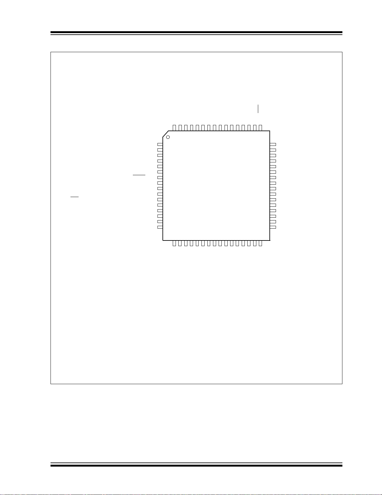
Pin Diagram – 64-Pin TQFP/QFN (PIC16F/LF1946/47)
1
2
3
4
5
6
7
8
9
10
11
12
13
14
38
37
36
35
34
33
50 49
17 18 19 20 21 22 23 24 25 26
RE2/P2B
(1)
/VLCD3
RE3/P3C
(1)
/COM0
RE4/P3B
(1)
/COM1
RE5/P1C
(1)
/COM2
RE6/P1B
(1)
/COM3
RE7/CCP2
(2)
/P2A
(2)
/SEG31
RD0/P2D
(2)
/SEG0
V
DD
VSS
RD1/P2C
(2)
/SEG1
RD2/P2B
(2)
/SEG2
RD3/P3C
(2)
/SEG3
RD4/SDO2/P3B
(2)
/SEG4
RD5/SDI2/SDA2/P1C
(2)
/SEG5
RD6/SCK2/SCL2/P1B
(2)
/SEG6
RD7/SS2
/SEG7
VLCD2/P2C
(1)
/RE1
VLCD1/P2D
(1)
/RE0
SEG42/P3A/CCP3/RG0
SEG43/C3OUT/CK2/TX2/CPS15/AN15/RG1
SEG44/C3IN+/DT2/RX2/CPS14/AN14/RG2
SEG45/P3D/CCP4/C3IN0-/CPS13/AN13/RG3
V
PP/MCLR/RG5
SEG26/P1D/CCP5/C3IN1-/CPS12/AN12/RG4
V
SS
VDD
SEG25/SS1/C1IN3-/C2IN3-/C3IN3-/CPS5/AN5/RF7
SEG24/C1IN+/CPS11/AN11/RF6
SEG23/DACOUT/C1IN1-/C2IN1-/CPS10/AN10/RF5
SEG22/C2IN+/CPS9/AN9/RF4
SEG21/C1IN2-/C2IN2-/C3IN2-/CPS8/AN8/RF3
SEG20/SRQ/C1OUT/CPS7/AN7/RF2
RB0/INT/SRI/FLT0/SEG30
RB1/SEG8
RB2/SEG9
RB3/SEG10
RB4/SEG11
RB5/T1G/SEG29
RB6/ICSPCLK/ICDCLK/SEG38
V
SS
RA6/OSC2/CLKOUT/SEG36
RA7/OSC1/CLKIN/SEG37
V
DD
RB7/ICSPDAT/ICDDAT/SEG39
RC4/SDI1/SDA1/SEG16
RC3/SCK1/SCL1/SEG17
RC2/CCP1/P1A/SEG13
VCAP/SEG41/C1IN0-/C2IN0-/CPS16/AN16/RF0
SEG19/SRNQ/C2OUT/CPS6/AN6/RF1
AV
DD
AVSS
SEG35/CPS3/VREF+/AN3/RA3
SEG34/CPS2/V
REF-/AN2/RA2
SEG18/CPS1/AN1/RA1
SEG33/CPS0/AN0/RA0
V
SS
VDD
SEG14/T0CKI/RA4
SEG15/CPS4/AN4/RA5
SEG32/CCP2
(1)
/P2A
(1)/
/T1OSI/RC1
SEG40/T1CKI/T1OSO/RC0
SEG28/DT1/RX1/RC7
SEG27/CK1/TX1/RC6
RC5/SDO1/SEG12
15
16
31
40
39
27 28
29 30 32
48
47
46
45
44
43
42
41
54 53 52 5158 57 56 5560 59
64
63 62 61
64-pin TQFP, QFN
Note 1: Pin location selected by APFCON register setting. Default location.
2: Pin function can be moved using the APFCON register. Alternate location.
3: QFN package orientation is the same. No leads are present on the QFN package.
PIC16F/LF1946/47
PIC16F/LF1946/47
2010 Microchip Technology Inc. Preliminary DS41414B-page 5
PIC16F/LF1946/47
TABLE 1: 64-PIN SUMMARY(PIC16F/LF1946/47)
I/O
64-Pin TQFP, QFN
RA0 24 Y AN0 — CPS0 — — — — — — SEG33 — — —
RA1 23 Y AN1 — CPS1 — — — — — — SEG18 — — —
RA2 22 Y AN2 VREF- CPS2 — — — — — — SEG34 — — —
RA3 21 Y AN3 V
RA4 28 — — — — — — T0CKI — — — SEG14 — — —
RA5 27 Y AN4 — CPS4 — — — — — — SEG15 — — —
RA6 40 — — — — — — — — — — SEG36 — — OSC2/
RA739——— ———— — ——SEG37——OSC1/
RB0 48 — — — — — SRI — FLT0 — — SEG30 INT/
RB147——— ———— — ——SEG8IOCY —
RB2 46 — — — — — — — — — — SEG9 IOC Y —
RB345——— ———— — ——SEG10IOCY —
RB4 44 — — — — — — — — — — SEG11 IOC Y —
RB543——— ———T1G— ——SEG29IOCY —
RB6 42 — — — — — — — — — — SEG38 IOC Y ICSP-
RB7 37 — — — — — — — — — — SEG39 IOC Y ICSP-
RC0 30 — — — — — — T1OSO/
RC1 29 — — — — — — T1OSI CCP2
RC2 33 — — — — — — — CCP1/
RC334—————————SCK1/
RC4 35 — — — — — — — — — SDI1/
RC536——— ———— — —SDO1SEG12———
RC6 31 — — — — — — — — TX1/
RC732——— ———— —RX1/
RD0 58 — — — — — — — P2D
RD155——— ————P2C
RD2 54 — — — — — — — P2B
RD353——— ————
RD4 52 — — — — — — — P3B
RD551——— ————P1C
RD6 50 — — — — — — — P1B
ANSEL
A/D
Reference
REF+ CPS3 — — — — — — SEG35 — — —
Cap Sense
Comparator
SR Latch
Timers
T1CKI
CCP
— — — SEG40 — — —
(1)
(1)
P2A
P1A
(2)
(2)
(2)
(2)
P3C
(2)
(2)
(2)
USART
/
— — SEG32 — — —
— — SEG13 — — —
SCL1
SDA1
CK1
DT1
— SEG27 — — —
— SEG28 — — —
— — SEG0 — — —
— — SEG1 — — —
— — SEG2 — — —
— — SEG3 — — —
— SDO2 SEG4 — — —
—SDI2
SDA2
— SCK2/
SCL2
LCD
MSSP
SEG17 — — —
SEG16 — — —
SEG5 — — —
SEG6 — — —
Interrupt
IOC
Pull-up
CLKOUT
CLKIN
Y —
CLK/
ICDCLK
DAT/
ICDDAT
Basic
Note 1: Pin functions can be moved using the APFCON register(s). Default location.
2: Pin function can be moved using the APFCON register. Alternate location.
3: Weak pull-up always enabled when MCLR
is enabled, otherwise the pull-up is under user control.
4: See Section 8.0.
DS41414B-page 6 Preliminary 2010 Microchip Technology Inc.
PIC16F/LF1946/47
TABLE 1: 64-PIN SUMMARY(PIC16F/LF1946/47) (Continued)
I/O
64-Pin TQFP, QFN
RD749—————————SS2SEG7 — — —
RE0 2 Y — — — — — — P2D
RE11Y—— ————P2C
RE2 64 Y — — — — — — P2B
RE363——— ————P3C
RE4 62 — — — — — — — P3B
RE561——— ————P1C
RE6 60 — — — — — — — P1B
RE759——— ————
RF0 18 Y AN16 — CPS16 C1IN0-
RF1 17 Y AN6 — CPS6 C2OUT SRNQ —
RF2 16 Y AN7 — CPS7 C1OUT SRQ — — — — SEG20 — — —
RF3 15 Y AN8 CPS8 C1IN2-
RF4 14 Y AN9 — CPS9 C2IN+ — — — — — SEG22 — — —
RF5 13 Y AN10 DACOUT CPS10 C1IN1-
RF6 12 Y AN11 — CPS11 C1IN+ — — — — — SEG24 — — —
RF7 11 Y AN5 — CPS5 C1IN3-
RG0 3 — — — — — — — CCP3
RG1 4 Y AN15 — CPS15 C3OUT — — — TX2/
RG2 5 Y AN14 — CPS14 C3IN+ — — — RX2/
RG3 6 Y AN13 — CPS13 C3IN0- — — CCP4
RG4 8 Y AN12 — CPS12 C3IN1- — — CCP5
RG57————————————
VDD 10
26
38
57
VSS 9
25
41
56
AVDD 19 — — — — — — — — — — — — — AVDD
AVSS 20——— ———— — —————AVSS
A/D
ANSEL
— — — — — — — — — — — — — VDD
——— ———— — —————VSS
Reference
Cap Sense
Comparator
C2IN0-
C2IN2C3IN2-
C2IN1-
C2IN3C3IN3-
SR Latch
— — — — — SEG41 — — VCAP
—— — ——SEG21———
—
————SS1
Timers
CCP2
P2A
—
—
P3A
P3D
P1D
CCP
(1)
(1)
(1)
(1)
(1)
(1)
(1)
(2)
(2)
USART
— VLCD1 — — —
——VLCD2———
— — VLCD3 — — —
——COM0———
— — COM1 — — —
——COM2———
— — COM3 — — —
/
— — SEG31 — — —
— — SEG19 — — —
— — SEG23 — — —
— — SEG42 — — —
CK2
DT2
— SEG43 — — —
— SEG44 — — —
——
— — SEG26 — — —
LCD
MSSP
SEG25 — — —
SEG45
Interrupt
———
Y
Pull-up
(2)
MCLR/
PP
V
Note 1: Pin functions can be moved using the APFCON register(s). Default location.
2: Pin function can be moved using the APFCON register. Alternate location.
3: Weak pull-up always enabled when MCLR
is enabled, otherwise the pull-up is under user control.
4: See Section 8.0.
Basic
(3)
2010 Microchip Technology Inc. Preliminary DS41414B-page 7

PIC16F/LF1946/47
Table of Contents
1.0 Device Overview ........................................................................................................................................................................ 11
2.0 Enhanced Mid-Range CPU ........................................................................................................................................................ 19
3.0 Memory Organization ................................................................................................................................................................. 21
4.0 Device Configuration.................................................................................................................................................................. 55
5.0 Oscillator Module (With Fail-Safe Clock Monitor)....................................................................................................................... 61
6.0 Resets ........................................................................................................................................................................................ 79
7.0 Interrupts .................................................................................................................................................................................... 87
8.0 Low Dropout (LDO) Voltage Regulator .................................................................................................................................... 103
9.0 Power-Down Mode (Sleep) ...................................................................................................................................................... 105
10.0 Watchdog Timer ....................................................................................................................................................................... 107
11.0 Data EEPROM and Flash Program Memory Control ............................................................................................................... 111
12.0 I/O Ports ................................................................................................................................................................................... 125
13.0 Interrupt-On-Change ................................................................................................................................................................ 151
14.0 Fixed Voltage Reference (FVR) ............................................................................................................................................... 155
15.0 Temperature Indicator Module ................................................................................................................................................. 157
16.0 Analog-to-Digital Converter (ADC) Module .............................................................................................................................. 159
17.0 Digital-to-Analog Converter (DAC) Module .............................................................................................................................. 173
18.0 Comparator Module.................................................................................................................................................................. 177
19.0 SR Latch................................................................................................................................................................................... 187
20.0 Timer0 Module ......................................................................................................................................................................... 193
21.0 Timer1 Module with Gate Control............................................................................................................................................. 197
22.0 Timer2/4/6 Modules.................................................................................................................................................................. 209
23.0 Capture/Compare/PWM Modules ............................................................................................................................................ 213
24.0 Master Synchronous Serial Port (MSSP1 and MSSP2) Module .............................................................................................. 243
25.0 Enhanced Universal Synchronous Asynchronous Receiver Transmitter (EUSART) ............................................................... 297
26.0 Capacitive Sensing (CPS) Module ........................................................................................................................................... 325
27.0 Liquid Crystal Display (LCD) Driver Module ............................................................................................................................. 335
28.0 In-Circuit Serial Programming™ (ICSP™) ............................................................................................................................... 371
29.0 Instruction Set Summary.......................................................................................................................................................... 375
30.0 Electrical Specifications............................................................................................................................................................ 389
31.0 DC and AC Characteristics Graphs and Charts ....................................................................................................................... 423
32.0 Development Support............................................................................................................................................................... 425
33.0 Packaging Information.............................................................................................................................................................. 429
Appendix A: Data Sheet Revision History .......................................................................................................................................... 435
Appendix B: Migrating From Other PIC
Index .................................................................................................................................................................................................. 437
The Microchip Web Site..................................................................................................................................................................... 445
Customer Change Notification Service .............................................................................................................................................. 445
Customer Support .............................................................................................................................................................................. 445
Reader Response .............................................................................................................................................................................. 446
Product Identification System............................................................................................................................................................. 447
®
Devices.............................................................................................................................. 435
DS41414B-page 8 Preliminary 2010 Microchip Technology Inc.

PIC16F/LF1946/47
TO OUR VALUED CUSTOMERS
It is our intention to provide our valued customers with the best documentation possible to ensure successful use of your Microchip
products. To this end, we will continue to improve our publications to better suit your needs. Our publications will be refined and
enhanced as new volumes and updates are introduced.
If you have any questions or comments regarding this publication, please contact the Marketing Communications Department via
E-mail at docerrors@microchip.com or fax the Reader Response Form in the back of this data sheet to (480) 792-4150. We
welcome your feedback.
Most Current Data Sheet
To obtain the most up-to-date version of this data sheet, please register at our Worldwide Web site at:
http://www.microchip.com
You can determine the version of a data sheet by examining its literature number found on the bottom outside corner of any page.
The last character of the literature number is the version number, (e.g., DS30000A is version A of document DS30000).
Errata
An errata sheet, describing minor operational differences from the data sheet and recommended workarounds, may exist for current
devices. As device/documentation issues become known to us, we will publish an errata sheet. The errata will specify the revision
of silicon and revision of document to which it applies.
To determine if an errata sheet exists for a particular device, please check with one of the following:
• Microchip’s Worldwide Web site; http://www.microchip.com
• Your local Microchip sales office (see last page)
When contacting a sales office, please specify which device, revision of silicon and data sheet (include literature number) you are
using.
Customer Notification System
Register on our web site at www.microchip.com to receive the most current information on all of our products.
2010 Microchip Technology Inc. Preliminary DS41414B-page 9

PIC16F/LF1946/47
NOTES:
DS41414B-page 10 Preliminary 2010 Microchip Technology Inc.
1.0 DEVICE OVERVIEW
The PIC16F/LF1946/47 are described within this data
sheet. They are available in 64-pin packages.
Figure 1-1 shows a block diagram of the
PIC16F/LF1946/47 devices. Ta bl e 1 - 2 shows the pinout descriptions.
Reference Tab le 1 -1 for peripherals available per
device.
TABLE 1-1: DEVICE PERIPHERAL
SUMMARY
Peripheral
PIC16F/LF1946/47
PIC16F1946/47
ADC ●●
Capacitive Sensing (CPS) Module ●●
Data EEPROM ●●
Digital-to-Analog Converter (DAC) ●●
Fixed Voltage Reference (FVR) ●●
LCD ●●
SR Latch ●●
Capture/Compare/PWM Modules
ECCP1 ●●
ECCP2 ●●
ECCP3 ●●
CCP4 ●●
CCP5 ●●
Comparators
C1 ●●
C2 ●●
C3 ●●
EUSARTS
EUSART1 ●●
EUSART2 ●●
Master Synchronous Serial Ports
MSSP1 ●●
MSSP2 ●●
Timers
Timer0 ●●
Timer1 ●●
Timer2 ●●
Timer4 ●●
Timer6 ●●
PIC16LF1946/47
2010 Microchip Technology Inc. Preliminary DS41414B-page 11
PIC16F/LF1946/47
PORTA
EUSARTx
Comparators
MSSPx
Timer2Timer1 Timer4Timer0
ECCP1
ADC
10-Bit
ECCP2 ECCP3
CCP4 CCP5
Timer6
PORTB
PORTC
PORTD
PORTE
LCD
SR
Latch
Note 1: See applicable chapters for more information on peripherals.
CPU
Program
Flash Memory
EEPROM
RAM
Timing
Generation
INTRC
Oscillator
MCLR
Figure 2-1
OSC1/CLKIN
OSC2/CLKOUT
PORTF
PORTG
FIGURE 1-1: PIC16F/LF1946/47 BLOCK DIAGRAM
DS41414B-page 12 Preliminary 2010 Microchip Technology Inc.
PIC16F/LF1946/47
TABLE 1-2: PIC16F/LF1946/47 PINOUT DESCRIPTION
Input
Name Function
RA0/AN0/CPS0/SEG33 RA0 TTL CMOS General purpose I/O.
AN0 AN — A/D Channel 0 input.
CPS0 AN — Capacitive sensing input 0.
SEG33 — AN LCD Analog output.
RA1/AN1/CPS1/SEG18 RA1 TTL CMOS General purpose I/O.
AN1 AN — A/D Channel 1 input.
CPS1 AN — Capacitive sensing input 1.
SEG18 — AN LCD Analog output.
RA2/AN2/V
RA3/AN3/V
RA4/T0CKI/SEG14 RA4 TTL CMOS General purpose I/O.
RA5/AN4/CPS4/SEG15 RA5 TTL CMOS General purpose I/O.
RA6/OSC2/CLKOUT/SEG36 RA6 TTL CMOS General purpose I/O.
RA7/OSC1/CLKIN/SEG37 RA7 TTL CMOS General purpose I/O.
RB0/INT/SRI/FLT0/SEG30 RB0 TTL CMOS General purpose I/O. Individually controlled interrupt-on-change.
RB1/SEG8 RB1 TTL CMOS General purpose I/O. Individually controlled interrupt-on-change.
Legend: AN = Analog input or output CMOS= CMOS compatible input or output OD = Open Drain
Note 1: Pin function is selectable via the APFCON register.
REF-/CPS2/SEG34 RA2 TTL CMOS General purpose I/O.
AN2 AN — A/D Channel 2 input.
REF- AN — A/D Negative Voltage Reference input.
V
CPS2 AN — Capacitive sensing input 2.
SEG34 — AN LCD Analog output.
REF+/CPS3/SEG35 RA3 TTL CMOS General purpose I/O.
AN3 AN — A/D Channel 3 input.
REF+ AN — A/D Voltage Reference input.
V
CPS3 AN — Capacitive sensing input 3.
SEG35 — AN LCD Analog output.
T0CKI ST — Timer0 clock input.
SEG14 — AN LCD Analog output.
AN4 AN — A/D Channel 4 input.
CPS4 AN — Capacitive sensing input 4.
SEG5 — AN LCD Analog output.
OSC2 — XTAL Crystal/Resonator (LP, XT, HS modes).
CLKOUT — CMOS F
SEG36 — AN LCD Analog output.
OSC1 XTAL — Crystal/Resonator (LP, XT, HS modes).
CLKIN CMOS — External clock input (EC mode).
SEG37 — AN LCD Analog output.
INT ST — External interrupt.
SRI — ST SR Latch input.
FLT0 ST — ECCP Auto-shutdown Fault input.
SEG30 — AN LCD analog output.
SEG8 — AN LCD Analog output.
TTL = TTL compatible input ST = Schmitt Trigger input with CMOS levels I
HV = High Voltage XTAL = Crystal levels
Type
Output
Type
OSC/4 output.
Individually enabled pull-up.
Individually enabled pull-up.
Description
2
C™ = Schmitt Trigger input with I2C
2010 Microchip Technology Inc. Preliminary DS41414B-page 13
PIC16F/LF1946/47
TABLE 1-2: PIC16F/LF1946/47 PINOUT DESCRIPTION (CONTINUED)
Input
Name Function
RB2/SEG9 RB2 TTL CMOS General purpose I/O. Individually controlled interrupt-on-change.
SEG9 — AN LCD Analog output.
RB3/SEG10 RB3 TTL CMOS General purpose I/O. Individually controlled interrupt-on-change.
SEG10 — AN LCD Analog output.
RB4/SEG11 RB4 TTL CMOS General purpose I/O. Individually controlled interrupt-on-change.
SEG11 — AN LCD Analog output.
RB5/T1G/SEG29 RB5 TTL CMOS General purpose I/O. Individually controlled interrupt-on-change.
T1G ST — Timer1 Gate input.
SEG29 — AN LCD Analog output.
RB6/ICSPCLK/ICDCLK/SEG38 RB6 TTL CMOS General purpose I/O. Individually controlled interrupt-on-change.
ICSPCLK ST — Serial Programming Clock.
ICDCLK ST — In-Circuit Debug Clock.
SEG38 — AN LCD Analog output.
RB7/ICSPDAT/ICDDAT/SEG39 RB7 TTL CMOS General purpose I/O. Individually controlled interrupt-on-change.
ICSPDAT ST CMOS ICSP™ Data I/O.
ICDDAT ST CMOS In-Circuit Data I/O.
SEG39 — AN LCD Analog output.
RC0/T1OSO/T1CKI/SEG40 RC0 ST CMOS General purpose I/O.
T1OSO XTAL XTAL Timer1 oscillator connection.
T1CKI ST — Timer1 clock input.
RC1/T1OSI/P2A
SEG32
RC2/CCP1/P1A/SEG13 RC2 ST CMOS General purpose I/O.
RC3/SCK/SCL/SEG17 RC3 ST CMOS General purpose I/O.
RC4/SDI1/SDA1/SEG16 RC4 ST CMOS General purpose I/O.
Legend: AN = Analog input or output CMOS= CMOS compatible input or output OD = Open Drain
Note 1: Pin function is selectable via the APFCON register.
(1)
TTL = TTL compatible input ST = Schmitt Trigger input with CMOS levels I
HV = High Voltage XTAL = Crystal levels
/CCP2
(1)
/
SEG40 — AN LCD Analog output.
RC1 ST CMOS General purpose I/O.
T1OSI XTAL XTAL Timer1 oscillator connection.
P2A — CMOS PWM output.
CCP2 ST CMOS Capture/Compare/PWM2.
SEG32 — AN LCD Analog output.
CCP1 ST CMOS Capture/Compare/PWM1.
P1A — CMOS PWM output.
SEG13 — AN LCD Analog output.
SCK ST CMOS SPI clock.
SCL I
SEG17 — AN LCD Analog output.
SDI1 ST — SPI data input.
SDA1 I
SEG16 — AN LCD Analog output.
Output
Type
Type
Individually enabled pull-up.
Individually enabled pull-up.
Individually enabled pull-up.
Individually enabled pull-up.
Individually enabled pull-up.
Individually enabled pull-up.
2
CODI2C™ clock.
2
CODI2C™ data input/output.
Description
2
C™ = Schmitt Trigger input with I2C
DS41414B-page 14 Preliminary 2010 Microchip Technology Inc.
PIC16F/LF1946/47
TABLE 1-2: PIC16F/LF1946/47 PINOUT DESCRIPTION (CONTINUED)
Input
Name Function
RC5/SDO1/SEG12 RC5 ST CMOS General purpose I/O.
SDO1 — CMOS SPI data output.
SEG12 — AN LCD Analog output.
RC6/TX1/CK1/SEG27 RC6 ST CMOS General purpose I/O.
TX1 — CMOS USART1 asynchronous transmit.
CK1 ST CMOS USART1 synchronous clock.
SEG27 — AN LCD Analog output.
RC7/RX1/DT1/SEG28 RC7 ST CMOS General purpose I/O.
RX ST — USART1 asynchronous input.
DT1 ST CMOS USART1 synchronous data.
SEG28 — AN LCD Analog output.
(1)
RD0/P2D
/SEG0 RD0 ST CMOS General purpose I/O.
P2D — CMOS PWM output.
SEG0 — AN LCD Analog output.
(1)
RD1/P2C
/SEG1 RD1 ST CMOS General purpose I/O.
P2C — CMOS PWM output.
SEG1 — AN LCD Analog output.
(1)
RD2/P2B
/SEG2 RD2 ST CMOS General purpose I/O.
P2B — CMOS PWM output.
SEG2 — AN LCD Analog output.
(1)
RD3/P3C
/SEG3 RD3 ST CMOS General purpose I/O.
P3C — CMOS PWM output.
SEG3 — AN LCD analog output.
(1)
RD4/SDO2/P3B
/SEG4 RD4 ST CMOS General purpose I/O.
SDO2 — CMOS SPI data output.
P3B — CMOS PWM output.
SEG4 — AN LCD analog output.
(1)
RD5/SDI2/SDA2/P1C
/SEG5 RD5 ST CMOS General purpose I/O.
SDI2 ST — SPI data input.
SDA2 I
P1C — CMOS PWM output.
SEG5 — AN LCD analog output.
(1)
RD6/SCK2/SCL2/P1B
/SEG6 RD6 ST CMOS General purpose I/O.
SCK2 ST CMOS SPI clock.
SCL2 I
P1B — CMOS PWM output.
SEG6 — AN LCD analog output.
RD7/SS2
/SEG7 RD7 ST CMOS General purpose I/O.
SS2
SEG7 — AN LCD analog output.
(1)
RE0/P2D
/VLCD1 RE0 ST CMOS General purpose I/O.
P2D — CMOS PWM output.
VLCD1 AN — LCD analog input.
Legend: AN = Analog input or output CMOS= CMOS compatible input or output OD = Open Drain
TTL = TTL compatible input ST = Schmitt Trigger input with CMOS levels I
HV = High Voltage XTAL = Crystal levels
Note 1: Pin function is selectable via the APFCON register.
Output
Type
Type
2
CODI2C™ data input/output.
2
CODI2C™ clock.
ST — Slave Select input.
Description
2
C™ = Schmitt Trigger input with I2C
2010 Microchip Technology Inc. Preliminary DS41414B-page 15
PIC16F/LF1946/47
TABLE 1-2: PIC16F/LF1946/47 PINOUT DESCRIPTION (CONTINUED)
Input
Name Function
RE1/P2C
(1)
/VLCD2 RE1 ST CMOS General purpose I/O.
P2C — CMOS PWM output.
VLCD2 AN — LCD analog input.
(1)
RE2/P2B
/VLCD3 RE2 ST CMOS General purpose I/O.
P2B — CMOS PWM output.
VLCD3 AN — LCD analog input.
(1)
RE3/P3C
/COM0 RE3 TTL — General purpose input.
P3C — CMOS PWM output.
COM0 — AN LCD Analog output.
(1)
RE4/P3B
/COM1 RE4 TTL — General purpose input.
P3B — CMOS PWM output.
COM1 — AN LCD Analog output.
(1)
RE5/P1C
/COM2 RE5 TTL — General purpose input.
P1C — CMOS PWM output.
COM2 — AN LCD Analog output.
(1)
RE6/P1B
/COM3 RE6 TTL — General purpose input.
P1B — CMOS PWM output.
COM3 — AN LCD Analog output.
(1)
(1)
/P2A
RE7/CCP2
/SEG31 RE7 TTL — General purpose input.
CCP2 ST CMOS Capture/Compare/PWM2.
P2A — CMOS PWM output.
SEG31 — AN LCD analog output.
RF0/AN16/CPS16/C12IN0-/
SEG41/V
CAP
RF0 TTL CMOS General purpose I/O.
AN16 AN — A/D Channel 16 input.
CPS16 AN — Capacitive sensing input 16.
C1IN0-
C2IN0-
SEG41 — AN LCD Analog output.
V
CAP Power Power Filter capacitor for Voltage Regulator.
RF1/AN6/CPS6/C2OUT/SRNQ/
SEG19
RF1 TTL CMOS General purpose I/O.
AN6 AN — A/D Channel 6 input.
CPS6 AN — Capacitive sensing input 6.
C2OUT — CMOS Comparator C2 output.
SRNQ — CMOS SR Latch inverting output.
SEG19 — AN LCD Analog output.
RF2/AN7/CPS7/C1OUT/SRQ/
SEG20
RF2 TTL CMOS General purpose I/O.
AN7 AN — A/D Channel 7 input.
CPS7 AN — Capacitive sensing input 7.
C1OUT — CMOS Comparator C1 output.
SRQ
SEG20 — AN LCD Analog output.
Legend: AN = Analog input or output CMOS= CMOS compatible input or output OD = Open Drain
TTL = TTL compatible input ST = Schmitt Trigger input with CMOS levels I
HV = High Voltage XTAL = Crystal levels
Note 1: Pin function is selectable via the APFCON register.
Output
Type
Type
AN — Comparator C1 negative input.
AN — Comparator C2 negative input.
CMOS SR Latch non-inverting output.
—
Description
2
C™ = Schmitt Trigger input with I2C
DS41414B-page 16 Preliminary 2010 Microchip Technology Inc.
PIC16F/LF1946/47
TABLE 1-2: PIC16F/LF1946/47 PINOUT DESCRIPTION (CONTINUED)
Input
Name Function
RF3/AN8/CPS8/C123IN2-/
SEG21
RF4/AN9/CPS9/C2IN+/SEG22 RF4 TTL CMOS General purpose I/O.
RF5/AN10/CPS10/C12IN1-/
DACOUT/SEG23
RF6/AN11/CPS11/C1IN+/SEG24 RF6 TTL CMOS General purpose I/O.
RF7/AN5/CPS5/C123IN3-/SS1
SEG25
RG0/CCP3/P3A/SEG42 RG0 ST CMOS General purpose I/O.
RG1/AN15/CPS15/TX2/CK2/
C3OUT/SEG43
Legend: AN = Analog input or output CMOS= CMOS compatible input or output OD = Open Drain
TTL = TTL compatible input ST = Schmitt Trigger input with CMOS levels I
HV = High Voltage XTAL = Crystal levels
Note 1: Pin function is selectable via the APFCON register.
RF3 TTL CMOS General purpose I/O.
AN8 AN — A/D Channel 8 input.
CPS8 AN — Capacitive sensing input 8.
C1IN2-
C2IN2-
C3IN2-
SEG21 — AN LCD Analog output.
AN9 AN — A/D Channel 9 input.
CPS9 AN — Capacitive sensing input 9.
C2IN+
SEG22 — AN LCD Analog output.
RF5 TTL CMOS General purpose I/O.
AN10 AN — A/D Channel 10 input.
CPS10 AN — Capacitive sensing input 10.
C1IN1-
C2IN1-
DACOUT — AN Voltage Reference output.
SEG23 — AN LCD Analog output.
AN11 AN — A/D Channel 11 input.
CPS11 AN — Capacitive sensing input 11.
C1IN+
SEG24 — AN LCD Analog output.
/
RF7 TTL CMOS General purpose I/O.
AN5 AN — A/D Channel 5 input.
CPS5 AN — Capacitive sensing input 5.
C1IN3-
C2IN3-
C3IN3-
SS1 ST — Slave Select input.
SEG25 — AN LCD Analog output.
CCP3 ST CMOS Capture/Compare/PWM3.
P3A — CMOS PWM output.
SEG42 — AN LCD Analog output.
RG1 ST CMOS General purpose I/O.
AN15 AN — A/D Channel 15 input.
CPS15 AN — Capacitive sensing input 15.
TX2 — CMOS USART2 asynchronous transmit.
CK2 ST CMOS USART2 synchronous clock.
C3OUT — CMOS Comparator C3 output.
SEG43 — AN LCD Analog output.
Output
Type
Type
AN — Comparator C1 negative input.
AN — Comparator C2 negative input.
AN — Comparator C3 negative input.
AN — Comparator C2 positive input.
AN — Comparator C1 negative input.
AN — Comparator C2 negative input.
AN — Comparator C1 positive input.
AN — Comparator C1negative input.
AN — Comparator C2 negative input.
AN — Comparator C3 negative input.
Description
2
C™ = Schmitt Trigger input with I2C
2010 Microchip Technology Inc. Preliminary DS41414B-page 17
PIC16F/LF1946/47
TABLE 1-2: PIC16F/LF1946/47 PINOUT DESCRIPTION (CONTINUED)
Input
Name Function
RG2/AN14/CPS14/RX2/DT2/
C3IN+/SEG44
RG3/AN13/CPS13/C3IN0-/
CCP4/P3D/SEG45
RG4/AN12/CPS12/C3IN1-/
CCP5/P1D/SEG26
RG5/MCLR
DD VDD Power — Positive supply.
V
V
SS VSS Power — Ground reference.
Legend: AN = Analog input or output CMOS= CMOS compatible input or output OD = Open Drain
Note 1: Pin function is selectable via the APFCON register.
/VPP RG5 TTL — General purpose input.
TTL = TTL compatible input ST = Schmitt Trigger input with CMOS levels I
HV = High Voltage XTAL = Crystal levels
RG2 ST CMOS General purpose I/O.
AN14 AN — A/D Channel 14 input.
CPS14 AN — Capacitive sensing input 14.
RX2 ST — USART2 asynchronous input.
DT2 ST CMOS USART2 synchronous data.
C3IN+
SEG44 — AN LCD Analog output.
RG3 ST CMOS General purpose I/O.
AN13 AN — A/D Channel 13 input.
CPS13 AN — Capacitive sensing input 13.
C3IN0-
CCP4 ST CMOS Capture/Compare/PWM4.
P3D — CMOS PWM output.
SEG45 — AN LCD Analog output.
RG4 ST CMOS General purpose I/O.
AN12 AN — A/D Channel 12 input.
CPS12 AN — Capacitive sensing input 12.
C3IN1-
CCP5 ST CMOS Capture/Compare/PWM5.
P1D — CMOS PWM output.
SEG26 — AN LCD Analog output.
MCLR
PP HV — Programming voltage.
V
Output
Type
Type
AN — Comparator C3 positive input.
AN — Comparator C3 negative input.
AN — Comparator C3 negative input.
ST — Master Clear with internal pull-up.
Description
2
C™ = Schmitt Trigger input with I2C
DS41414B-page 18 Preliminary 2010 Microchip Technology Inc.

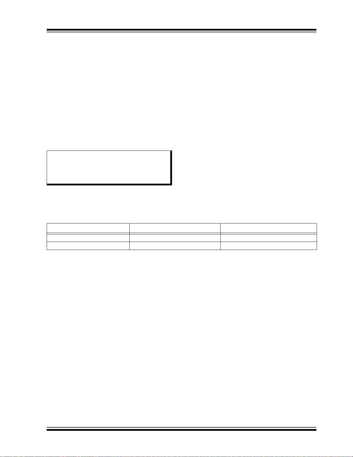
2.0 ENHANCED MID-RANGE CPU
This family of devices contain an enhanced mid-range
8-bit CPU core. The CPU has 49 instructions. Interrupt
capability includes automatic context saving. The
hardware stack is 16 levels deep and has Overflow and
Underflow Reset capability. Direct, Indirect, and
Relative addressing modes are available. Two File
Select Registers (FSRs) provide the ability to read
program and data memory.
• Automatic Interrupt Context Saving
• 16-level Stack with Overflow and Underflow
• File Select Registers
• Instruction Set
2.1 Automatic Interrupt Context Saving
During interrupts, certain registers are automatically
saved in shadow registers and restored when returning
from the interrupt. This saves stack space and user
code. See Section 7.5 “Automatic Context Saving”,
for more information.
PIC16F/LF1946/47
2.2 16-level Stack with Overflow and Underflow
These devices have an external stack memory 15 bits
wide and 16 words deep. A Stack Overflow or Underflow will set the appropriate bit (STKOVF or STKUNF)
in the PCON register, and if enabled will cause a software Reset. See section Section 3.4 “St ack” for more
details.
2.3 File Select Registers
There are two 16-bit File Select Registers (FSR). FSRs
can access all file registers and program memory,
which allows one data pointer for all memory. When an
FSR points to program memory, there is 1 additional
instruction cycle in instructions using INDF to allow the
data to be fetched. General purpose memory can now
also be addressed linearly, providing the ability to
access contiguous data larger than 80 bytes. There are
also new instructions to support the FSRs. See
Section 3.5 “Indirect Addressing” for more details.
2.4 Instruction Set
There are 49 instructions for the enhanced mid-range
CPU to support the features of the CPU. See
Section 29.0 “Instruction Set Summary” for more
details.
2010 Microchip Technology Inc. Preliminary DS41414B-page 19
PIC16F/LF1946/47
Data Bus
8
14
Program
Bus
Instruction reg
Program Counter
8 Level Stack
(13-bit)
Direct Addr
7
12
Addr MUX
FSR reg
STATUS reg
MUX
ALU
Power-up
Timer
Oscillator
Start-up Timer
Power-on
Reset
Watchdog
Timer
Instruction
Decode &
Control
Timing
Generation
OSC1/CLKIN
OSC2/CLKOUT
V
DD
8
8
Brown-out
Reset
12
3
VSS
Internal
Oscillator
Block
Configuration
Data Bus
8
14
Program
Bus
Instruction reg
Program Counter
8 Level Stack
(13-bit)
Direct Addr
7
Addr MUX
FSR reg
STATUS reg
MUX
ALU
W Reg
Instruction
Decode &
Control
Timing
Generation
V
DD
8
8
3
VSS
Internal
Oscillator
Block
Configuration
15
Data Bus
8
14
Program
Bus
Instruction Reg
Program Counter
16-Level Stack
(15-bit)
Direct Addr
7
RAM Addr
Addr MUX
Indirect
Addr
FSR0 Reg
STATUS Reg
MUX
ALU
Instruction
Decode and
Control
Timing
Generation
V
DD
8
8
3
VSS
Internal
Oscillator
Block
Configuration
Flash
Program
Memory
RAM
FSR regFSR reg
FSR1 Reg
15
15
MUX
15
Program Memory
Read (PMR)
12
FSR regFSR reg
BSR Reg
5
FIGURE 2-1: CORE BLOCK DIAGRAM
DS41414B-page 20 Preliminary 2010 Microchip Technology Inc.
PIC16F/LF1946/47
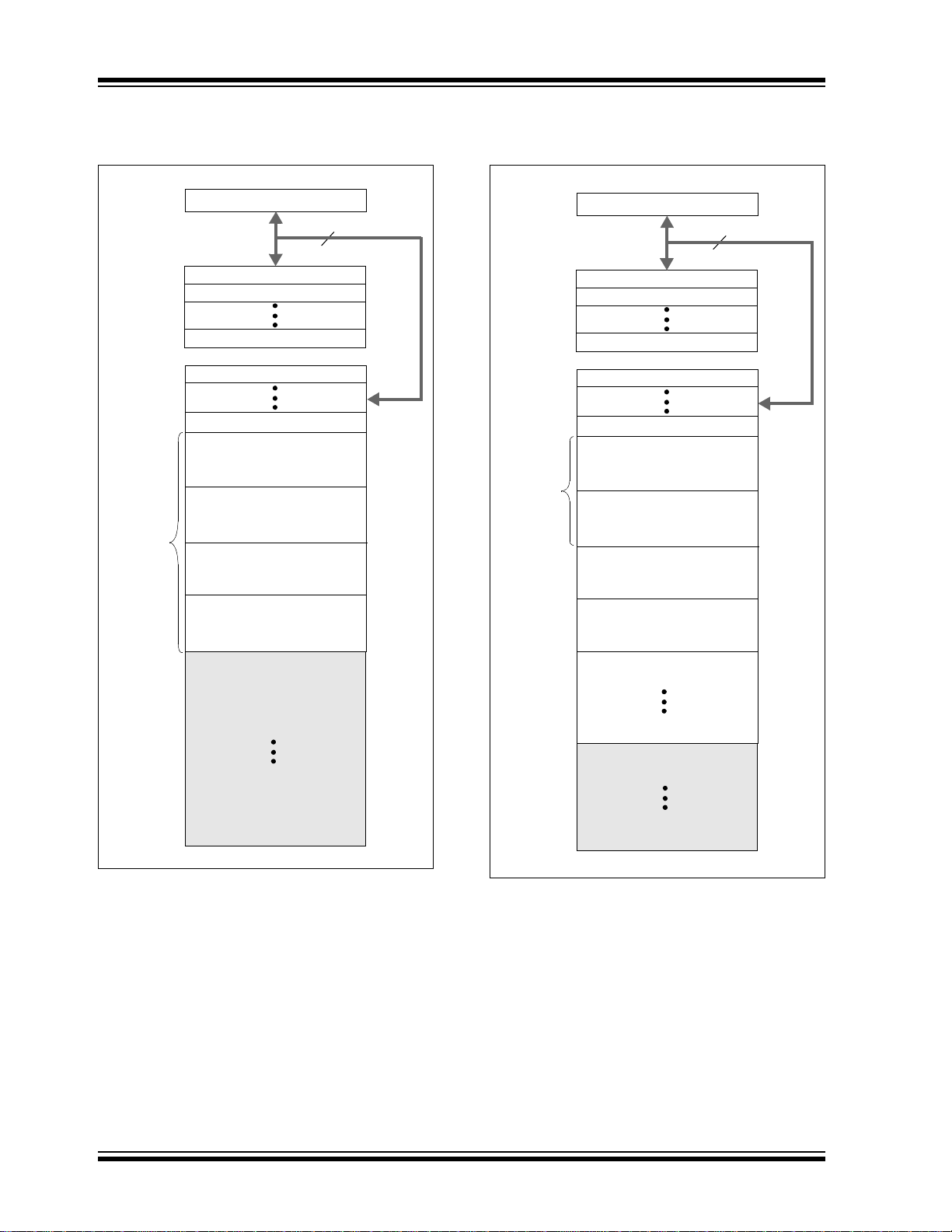
3.0 MEMORY ORGANIZATION
There are three types of memory in PIC16F/LF1946/47
devices: Data Memory, Program Memory and Data
EEPROM Memory
• Program Memory
• Data Memory
- Core Registers
- Special Function Registers
- General Purpose RAM
- Common RAM
- Device Memory Maps
- Special Function Registers Summary
• Data EEPROM memory
Note 1: The data EEPROM memory and the
(1)
.
(1)
method to access Flash memory through
the EECON registers is described in
Section 11.0 “Data EEPROM and Flash
Program Memory Control”.
The following features are associated with access and
control of program memory and data memory:
• PCL and PCLATH
•Stack
• Indirect Addressing
3.1 Program Memory Organization
The enhanced mid-range core has a 15-bit program
counter capable of addressing 32K x 14 program
memory space. Table 3-1 shows the memory sizes
implemented for the PIC16F/LF1946/47 family.
Accessing a location above these boundaries will cause
a wrap-around within the implemented memory space.
The Reset vector is at 0000h and the interrupt vector is
at 0004h (see Figures 3-1 and 3-2).
TABLE 3-1: DEVICE SIZES AND ADDRESSES
Device Program Memory Space (Words) Last Program Memory Address
PIC16F/LF1946 8,192 1FFFh
PIC16F/LF1947 16,384 3FFFh
2010 Microchip Technology Inc. Preliminary DS41414B-page 21
PIC16F/LF1946/47
PC<14:0>
15
0000h
0004h
Stack Level 0
Stack Level 15
Reset Vector
Interrupt Vector
Stack Level 1
0005h
On-chip
Program
Memory
Page 0
07FFh
Rollover to Page 0
0800h
0FFFh
1000h
7FFFh
Page 1
Rollover to Page 3
Page 2
Page 3
17FFh
1800h
1FFFh
2000h
CALL, CALLW
RETURN, RETLW
Interrupt, RETFIE
PC<14:0>
15
0000h
0004h
Stack Level 0
Stack Level 15
Reset Vector
Interrupt Vector
Stack Level 1
0005h
On-chip
Program
Memory
Page 0
07FFh
Rollover to Page 0
0800h
0FFFh
1000h
7FFFh
Page 1
Rollover to Page 7
Page 2
Page 3
17FFh
1800h
1FFFh
2000h
Page 4
Page 7
3FFFh
4000h
CALL, CALLW
RETURN, RETLW
Interrupt, RETFIE
FIGURE 3-1: PROGRAM MEMORY MAP
AND STACK FOR
PIC16F/LF1946
FIGURE 3-2: PROGRAM MEMORY MAP
AND STACK FOR
PIC16F/LF1947
DS41414B-page 22 Preliminary 2010 Microchip Technology Inc.

3.1.1 READING PROGRAM MEMORY AS
constants
BRW ;Add Index in W to
;program counter to
;select data
RETLW DATA0 ;Index0 data
RETLW DATA1 ;Index1 data
RETLW DATA2
RETLW DATA3
my_function
;… LOTS OF CODE…
MOVLW DATA_INDEX
CALL constants
;… THE CONSTANT IS IN W
DATA
There are two methods of accessing constants in program memory. The first method is to use tables of
RETLW instructions. The second method is to set an
FSR to point to the program memory.
3.1.1.1 RETLW Instruction
The RETLW instruction can be used to provide access
to tables of constants. The recommended way to create
such a table is shown in Example 3-1.
EXAMPLE 3-1: RETLW INSTRUCTION
PIC16F/LF1946/47
The BRW instruction makes this type of table very
simple to implement. If your code must remain portable
with previous generations of microcontrollers, then the
BRW instruction is not available so the older table read
method must be used.
2010 Microchip Technology Inc. Preliminary DS41414B-page 23

PIC16F/LF1946/47
constants
RETLW DATA0 ;Index0 data
RETLW DATA1 ;Index1 data
RETLW DATA2
RETLW DATA3
my_function
;… LOTS OF CODE…
MOVLW LOW constants
MOVWF FSR1L
MOVLW HIGH constants
MOVWF FSR1H
MOVIW 0[FSR1]
;THE PROGRAM MEMORY IS IN W
3.1.1.2 Indirect Read with FSR
The program memory can be accessed as data by setting bit 7 of the FSRxH register and reading the matching INDFx register. The MOVIW instruction will place the
lower 8 bits of the addressed word in the W register.
Writes to the program memory cannot be performed via
the INDF registers. Instructions that access the program memory via the FSR require one extra instruction
cycle to complete. Example 3-2 demonstrates accessing the program memory via an FSR.
The HIGH directive will set bit<7> if a label points to a
location in program memory.
EXAMPLE 3-2: ACCESSING PROGRAM
MEMORY VIA FSR
3.2.1 CORE REGISTERS
The core registers contain the registers that directly
affect the basic operation of the PIC16F/LF1946/47.
These registers are listed below:
• INDF0
• INDF1
•PCL
•STATUS
•FSR0 Low
• FSR0 High
•FSR1 Low
• FSR1 High
• BSR
•WREG
•PCLATH
• INTCON
Note: The core registers are the first 12
addresses of every data memory bank.
3.2 Data Memory Organization
The data memory is partitioned in 32 memory banks
with 128 bytes in a bank. Each bank consists of
(Figure 3-3):
• 12 core registers
• 20 Special Function Registers (SFR)
• Up to 80 bytes of General Purpose RAM (GPR)
• 16 bytes of common RAM
The active bank is selected by writing the bank number
into the Bank Select Register (BSR). Unimplemented
memory will read as ‘0’. All data memory can be
accessed either directly (via instructions that use the
file registers) or indirectly via the two File Select
Registers (FSR). See Section 3.5 “Indirect
Addressing” for more information.
DS41414B-page 24 Preliminary 2010 Microchip Technology Inc.
PIC16F/LF1946/47
3.2.1.1 STATUS Register
The STATUS register, shown in Register 3-1, contains:
• the arithmetic status of the ALU
• the Reset status
The STATUS register can be the destination for any
instruction, like any other register. If the STATUS
register is the destination for an instruction that affects
the Z, DC or C bits, then the write to these three bits is
disabled. These bits are set or cleared according to the
device logic. Furthermore, the TO
writable. Therefore, the result of an instruction with the
STATUS register as destination may be different than
intended.
and PD bits are not
For example, CLRF STATUS will clear the upper three
bits and set the Z bit. This leaves the STATUS register
as ‘000u u1uu’ (where u = unchanged).
It is recommended, therefore, that only BCF, BSF,
SWAPF and MOVWF instructions are used to alter the
STATUS register, because these instructions do not
affect any Status bits. For other instructions not
affecting any Status bits (Refer to Section 29.0
“Instruction Set Summary”).
Note 1: The C and DC bits operate as Borrow
and Digit Borrow out bits, respectively, in
subtraction.
REGISTER 3-1: STATUS: STATUS REGISTER
U-0 U-0 U-0 R-1/q R-1/q R/W-0/u R/W-0/u R/W-0/u
— — —
bit 7 bit 0
Legend:
R = Readable bit W = Writable bit U = Unimplemented bit, read as ‘0’
u = Bit is unchanged x = Bit is unknown -n/n = Value at POR and BOR/Value at all other Resets
‘1’ = Bit is set ‘0’ = Bit is cleared q = Value depends on condition
TO
PD ZDC
(1)
(1)
C
bit 7-5 Unimplemented: Read as ‘0’
bit 4 TO
bit 3 PD
bit 2 Z: Zero bit
bit 1 DC: Digit Carry/Digit Borrow
bit 0 C: Carry/Borrow
Note 1: For Borrow, the polarity is reversed. A subtraction is executed by adding the two’s complement of the
second operand. For rotate (RRF, RLF) instructions, this bit is loaded with either the high-order or low-order
bit of the source register.
: Time-out bit
1 = After power-up, CLRWDT instruction or SLEEP instruction
0 = A WDT time-out occurred
: Power-down bit
1 = After power-up or by the CLRWDT instruction
0 = By execution of the SLEEP instruction
1 = The result of an arithmetic or logic operation is zero
0 = The result of an arithmetic or logic operation is not zero
bit (ADDWF, ADDLW,SUBLW,SUBWF instructions)
1 = A carry-out from the 4th low-order bit of the result occurred
0 = No carry-out from the 4th low-order bit of the result
(1)
bit
(ADDWF, ADDLW, SUBLW, SUBWF instructions)
1 = A carry-out from the Most Significant bit of the result occurred
0 = No carry-out from the Most Significant bit of the result occurred
(1)
(1)
2010 Microchip Technology Inc. Preliminary DS41414B-page 25
PIC16F/LF1946/47
0Bh
0Ch
1Fh
20h
6Fh
70h
7Fh
00h
Common RAM
(16 bytes)
General Purpose RAM
(80 bytes maximum)
Core Registers
(12 bytes)
Special Function Registers
(20 bytes maximum)
Memory Region
7-bit Bank Offset
3.2.2 SPECIAL FUNCTION REGISTER
The Special Function Registers are registers used by
the application to control the desired operation of
peripheral functions in the device. The registers associated with the operation of the peripherals are
described in the appropriate peripheral chapter of this
data sheet.
3.2.3 GENERAL PURPOSE RAM
There are up to 80 bytes of GPR in each data memory
bank.
3.2.3.1 Linear Access to GPR
The general purpose RAM can be accessed in a
non-banked method via the FSRs. This can simplify
access to large memory structures. See Section 3.5.2
“Linear Data Memory” for more information.
3.2.4 COMMON RAM
There are 16 bytes of common RAM accessible from all
banks.
FIGURE 3-3: BANKED MEMORY
PARTITIONING
3.2.5 DEVICE MEMORY MAPS
The memory maps for the device family are as shown
in Table 3-2.
TABLE 3-2: MEMORY MAP TABLES
Device Banks Table No.
PIC16F/LF1946/47 0-7 Table 3-3
8-15 Table 3-4, Table 3-7
16-23 Table 3-5
23-31 Table 3-6, Table 3-8
DS41414B-page 26 Preliminary 2010 Microchip Technology Inc.
DS41414B-page 27 Preliminary 2010 Microchip Technology Inc.
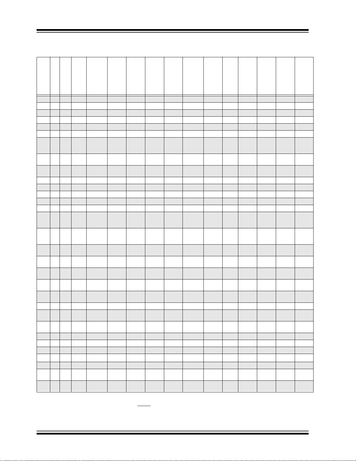
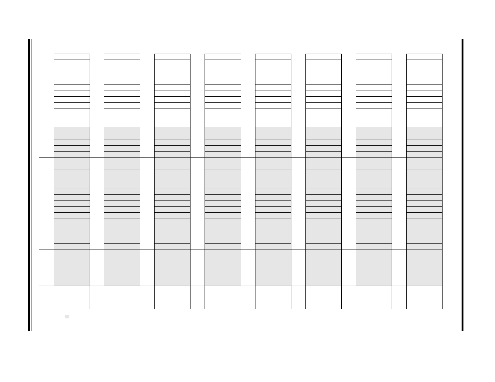
TABLE 3-3: PIC16F/LF1946/1947 MEMORY MAP, BANKS 0-7
PIC16F/LF1946/47
BANK 0 BANK 1 BANK 2 BANK 3 BANK 4 BANK 5 BANK 6 BANK 7
000h INDF0 080h INDF0 100h INDF0 180h INDF0 200h INDF0 280h INDF0 300h INDF0 380h INDF0
001h INDF1 081h INDF1 101h INDF1 181h INDF1 201h INDF1 281h INDF1 301h INDF1 381h INDF1
002h PCL 082h PCL 102h PCL 182h PCL 202h PCL 282h PCL 302h PCL 382h PCL
003h STATUS 083h STATUS 103h STATUS 183h STATUS 203h STATUS 283h STATUS 303h STATUS 383h STATUS
004h FSR0L 084h FSR0L 104h FSR0L 184h FSR0L 204h FSR0L 284h FSR0L 304h FSR0L 384h FSR0L
005h FSR0H 085h FSR0H 105h FSR0H 185h FSR0H 205h FSR0H 285h FSR0H 305h FSR0H 385h FSR0H
006h FSR1L 086h FSR1L 106h FSR1L 186h FSR1L 206h FSR1L 286h FSR1L 306h FSR1L 386h FSR1L
007h FSR1H 087h FSR1H 107h FSR1H 187h FSR1H 207h FSR1H 287h FSR1H 307h FSR1H 387h FSR1H
008h BSR 088h BSR 108h BSR 188h BSR 208h BSR 288h BSR 308h BSR 388h BSR
009h WREG 089h WREG 109h WREG 189h WREG 209h WREG 289h WREG 309h WREG 389h WREG
00Ah PCLATH 08Ah PCLATH 10Ah PCLATH 18Ah PCLATH 20Ah PCLATH 28Ah PCLATH 30Ah PCLATH 38Ah PCLATH
00Bh INTCON 08Bh INTCON 10Bh INTCON 18Bh INTCON 20Bh INTCON 28Bh INTCON 30Bh INTCON 38Bh INTCON
00Ch PORTA 08Ch TRISA 10Ch LATA 18Ch ANSELA 20Ch
00Dh PORTB 08Dh TRISB 10Dh LATB 18Dh
00Eh PORTC 08Eh TRISC 10Eh LATC 18Eh
00Fh PORTD 08Fh TRISD 10Fh LATD 18Fh
010h PORTE 090h TRISE 110h LATE 190h ANSELE 210h
011h PIR1 091h PIE1 111h CM1CON0 191h EEADRL 211h SSP1BUF 291h CCPR1L 311h CCPR3L 391h
012h PIR2 092h PIE2 112h CM1CON1 192h EEADRH 212h SSP1ADD 292h CCPR1H 312h CCPR3H 392h
013h PIR3 093h PIE3 113h CM2CON0 193h EEDATL 213h SSP1MSK 293h CCP1CON 313h CCP3CON 393h
014h PIR4 094h PIE4 114h CM2CON1 194h EEDATH 214h SSP1STAT 294h PWM1CON 314h PWM3CON 394h IOCBP
015h TMR0 095h OPTION 115h CMOUT 195h EECON1 215h SSP1CON1 295h CCP1AS 315h CCP3AS 395h IOCBN
016h TMR1L 096h PCON 116h BORCON 196h EECON2 216h SSP1CON2 296h PSTR1CON 316h PSTR3CON 396h IOCBF
017h TMR1H 097h WDTCON 117h FVRCON 197h
018h T1CON 098h OSCTUNE 118h DACCON0 198h
019h T1GCON 099h OSCCON 119h DACCON1 199h RC1REG 219h SSP2BUF 299h CCPR2H 319h CCPR4H 399h
01Ah TMR2 09Ah OSCSTAT 11Ah SRCON0 19Ah TX1REG 21Ah SSP2ADD 29Ah CCP2CON 31Ah CCP4CON 39Ah
01Bh PR2 09Bh ADRESL 11Bh SRCON1 19Bh SP1BRGL 21Bh SSP2MSK 29Bh PWM2CON 31Bh
01Ch T2CON 09Ch ADRESH 11Ch
01Dh
01Eh CPSCON0 09Eh ADCON1 11Eh CM3CON0 19Eh TX1STA 21Eh SSP2CON2 29Eh CCPTMRS0 31Eh CCP5CON 39Eh
01Fh CPSCON1 09Fh
020h
06Fh 0EFh 16Fh 1EFh 26Fh 2EFh
070h 0F0h
07Fh 0FFh 17Fh 1FFh 27Fh 2FFh 37Fh 3FFh
Legend: = Unimplemented data memory locations, read as ‘0’.
Note 1: Not available on PIC16F1946.
— 09Dh ADCON0 11Dh APFCON 19Dh RC1STA 21Dh SSP2CON1 29Dh PSTR2CON 31Dh CCPR5H 39Dh —
— 11Fh CM3CON1 19Fh BAUD1CON 21Fh SSP2CON3 29Fh CCPTMRS1 31Fh —39Fh—
General
Purpose
Register
80 Bytes
Accesses
70h – 7Fh
120h
170h
General
Purpose
Register
96 Bytes
0A0h
— 19Ch SP1BRGH 21Ch SSP2STAT 29Ch CCP2AS 31Ch CCPR5L 39Ch —
1A0h
General
Purpose
Register
80 Bytes
Accesses
70h – 7Fh
1F0h
— 20Dh WPUB 28Dh PORTG 30Dh TRISG 38Dh LATG
—20Eh—28Eh—30Eh—38Eh—
—20Fh—28Fh—30Fh—38Fh—
— 217h SSP1CON3 297h — 317h — 397h —
—218h— 298h CCPR2L 318h CCPR4L 398h —
220h
General
Purpose
Register
80 Bytes
Accesses
70h – 7Fh
270h
— 28Ch PORTF 30Ch TRISF 38Ch LATF
—290h— 310h — 390h —
—39Bh—
General
Purpose
Register
80 Bytes
Accesses
70h – 7Fh
2A0h
2F0h
General
Purpose
Register
80 Bytes
Accesses
70h – 7Fh
320h
General Purpose
Register
32Fh
330h
36Fh 3EFh
370h
16 Bytes
General Purpose
Register
64 Bytes
Accesses
70h – 7Fh
3A0h
(1)
3F0h
—
—
—
—
—
—
General
Purpose
Register
80 Bytes
Accesses
70h – 7Fh
(1)
DS41414B-page 28 Preliminary 2010 Microchip Technology Inc.
Legend: = Unimplemented data memory locations, read as ‘0’
Note 1: Not available on PIC16F1946.
BANK 8 BANK 9 BANK 10 BANK 11 BANK 12 BANK 13 BANK 14 BANK 15
400h
INDF0
480h
INDF0
500h
INDF0
580h
INDF0
600h
INDF0
680h
INDF0
700h
INDF0
780h
INDF0
401h
INDF1
481h
INDF1
501h
INDF1
581h
INDF1
601h
INDF1
681h
INDF1
701h
INDF1
781h
INDF1
402h
PCL
482h
PCL
502h
PCL
582h
PCL
602h
PCL
682h
PCL
702h
PCL
782h
PCL
403h
STATUS
483h
STATUS
503h
STATUS
583h
STATUS
603h
STATUS
683h
STATUS
703h
STATUS
783h
STATUS
404h
FSR0L
484h
FSR0L
504h
FSR0L
584h
FSR0L
604h
FSR0L
684h
FSR0L
704h
FSR0L
784h
FSR0L
405h
FSR0H
485h
FSR0H
505h
FSR0H
585h
FSR0H
605h
FSR0H
685h
FSR0H
705h
FSR0H
785h
FSR0H
406h
FSR1L
486h
FSR1L
506h
FSR1L
586h
FSR1L
606h
FSR1L
686h
FSR1L
706h
FSR1L
786h
FSR1L
407h
FSR1H
487h
FSR1H
507h
FSR1H
587h
FSR1H
607h
FSR1H
687h
FSR1H
707h
FSR1H
787h
FSR1H
408h
BSR
488h
BSR
508h
BSR
588h
BSR
608h
BSR
688h
BSR
708h
BSR
788h
BSR
409h
WREG
489h
WREG
509h
WREG
589h
WREG
609h
WREG
689h
WREG
709h
WREG
789h
WREG
40Ah
PCLATH
48Ah
PCLATH
50Ah
PCLATH
58Ah
PCLATH
60Ah
PCLATH
68Ah
PCLATH
70Ah
PCLATH
78Ah
PCLATH
40Bh
INTCON
48Bh
INTCON
50Bh
INTCON
58Bh
INTCON
60Bh
INTCON
68Bh
INTCON
70Bh
INTCON
78Bh
INTCON
40Ch
ANSELF
48Ch
—
50Ch
—
58Ch
—
60Ch
—
68Ch
—
70Ch
—
78Ch
—
40Dh
ANSELG
48Dh
WPUG
50Dh
—
58Dh
—
60Dh
—
68Dh
—
70Dh
—
78Dh
—
40Eh
—
48Eh
—
50Eh
—
58Eh
—
60Eh
—
68Eh
—
70Eh
—
78Eh
—
40Fh
—
48Fh
—
50Fh
—
58Fh
—
60Fh
—
68Fh
—
70Fh
—
78Fh
—
410h
—
490h
—
510h
—
590h
—
610h
—
690h
—
710h
—
790h
—
411h
—
491h
RC2REG
511h
—
591h
—
611h
—
691h
—
711h
—
791h
See Ta bl e 3 -7
412h
—
492h
TX2REG
512h
—
592h
—
612h
—
692h
—
712h
—
792h
413h
—
493h
SP2BRG
513h
—
593h
—
613h
—
693h
—
713h
—
793h
414h
—
494h
SP2BRGH
514h
—
594h
—
614h
—
694h
—
714h
—
794h
415h
TMR4
495h
RC2STA
515h
—
595h
—
615h
—
695h
—
715h
—
795h
416h
PR4
496h
TX2STA
516h
—
596h
—
616h
—
696h
—
716h
—
796h
417h
T4CON
497h
BAUDCON2
517h
—
597h
—
617h
—
697h
—
717h
—
797h
418h
—
498h
—
518h
—
598h
—
618h
—
698h
—
718h
—
798h
419h
—
499h
—
519h
—
599h
—
619h
—
699h
—
719h
—
799h
41Ah
—
49Ah
—
51Ah
—
59Ah
—
61Ah
—
69Ah
—
71Ah
—
79Ah
41Bh
—
49Bh
—
51Bh
—
59Bh
—
61Bh
—
69Bh
—
71Bh
—
79Bh
41Ch
TMR6
49Ch
—
51Ch
—
59Ch
—
61Ch
—
69Ch
—
71Ch
—
79Ch
41Dh
PR6
49Dh
—
51Dh
—
59Dh
—
61Dh
—
69Dh
—
71Dh
—
79Dh
41Eh
T6CON
49Eh
—
51Eh
—
59Eh
—
61Eh
—
69Eh
—
71Eh
—
79Eh
41Fh
—
49Fh
—
51Fh
—
59Fh
—
61Fh
—
69Fh
—
71Fh
—
79Fh
420h
General
Purpose
Register
80 Bytes
(1)
4A0h
General
Purpose
Register
80 Bytes
(1)
520h
General
Purpose
Register
80 Bytes
(1)
5A0h
General
Purpose
Register
80 Bytes
(1)
620h
General Purpose
Register
48 Bytes
(1)
6A0h
Unimplemented
Read as ‘0’
720h
Unimplemented
Read as ‘0’
7A0h
Unimplemented
Read as ‘0’
46Fh 4EFh 56Fh 5EFh 66Fh 6EFh 76Fh 7EFh
470h
Accesses
70h – 7Fh
4F0h
Accesses
70h – 7Fh
570h
Accesses
70h – 7Fh
5F0h
Accesses
70h – 7Fh
670h
Accesses
70h – 7Fh
6F0h
Accesses
70h – 7Fh
770h
Accesses
70h – 7Fh
7F0h
Accesses
70h – 7Fh
47Fh
4FFh 57Fh
5FFh 67Fh 6FFh 77Fh 7FFh
TABLE 3-4: PIC16F/LF1946/1947 MEMORY MAP, BANKS 8-15
PIC16F/LF1946/47
DS41414B-page 29 Preliminary 2010 Microchip Technology Inc.
TABLE 3-5: PIC16F/LF1946/47 MEMORY MAP, BANKS 16-23
PIC16F/LF1946/47
BANK 16 BANK 17 BANK 18 BANK 19 BANK 20 BANK 21 BANK 22 BANK 23
800h INDF0 880h INDF0 900h INDF0 980h INDF0 A00h INDF0 A80h INDF0 B00h INDF0 B80h INDF0
801h INDF1 881h INDF1 901h INDF1 981h INDF1 A01h INDF1 A81h INDF1 B01h INDF1 B81h INDF1
802h PCL 882h PCL 902h PCL 982h PCL A02h PCL A82h PCL B02h PCL B82h PCL
803h STATUS 883h STATUS 903h STATUS 983h STATUS A03h STATUS A83h STATUS B03h STATUS B83h STATUS
804h FSR0L 884h FSR0L 904h FSR0L 984h FSR0L A04h FSR0L A84h FSR0L B04h FSR0L B84h FSR0L
805h FSR0H 885h FSR0H 905h FSR0H 985h FSR0H A05h FSR0H A85h FSR0H B05h FSR0H B85h FSR0H
806h FSR1L 886h FSR1L 906h FSR1L 986h FSR1L A06h FSR1L A86h FSR1L B06h FSR1L B86h FSR1L
807h FSR1H 887h FSR1H 907h FSR1H 987h FSR1H A07h FSR1H A87h FSR1H B07h FSR1H B87h FSR1H
808h BSR 888h BSR 908h BSR 988h BSR A08h BSR A88h BSR B08h BSR B88h BSR
809h WREG 889h WREG 909h WREG 989h WREG A09h WREG A89h WREG B09h WREG B89h WREG
80Ah PCLATH 88Ah PCLATH 90Ah PCLATH 98Ah PCLATH A0Ah PCLATH A8Ah PCLATH B0Ah PCLATH B8Ah PCLATH
80Bh INTCON 88Bh INTCON 90Bh INTCON 98Bh INTCON A0Bh INTCON A8Bh INTCON B0Bh INTCON B8Bh INTCON
80Ch
80Dh
80Eh
80Fh
810h
811h
812h
813h
814h
815h
816h
817h
818h
819h
81Ah
81Bh
81Ch
81Dh
81Eh
81Fh
820h
— 88Ch — 90Ch — 98Ch —A0Ch—A8Ch—B0Ch—B8Ch—
— 88Dh — 90Dh — 98Dh —A0Dh—A8Dh—B0Dh—B8Dh—
—88Eh—90Eh—98Eh—A0Eh—A8Eh—B0Eh—B8Eh—
—88Fh—90Fh—98Fh—A0Fh—A8Fh—B0Fh—B8Fh—
—890h—910h—990h—A10h—A90h—B10h—B90h—
—891h—911h—991h—A11h—A91h—B11h—B91h—
—892h—912h—992h—A12h—A92h—B12h—B92h—
—893h—913h—993h—A13h—A93h—B13h—B93h—
—894h—914h—994h—A14h—A94h—B14h—B94h—
—895h—915h—995h—A15h—A95h—B15h—B95h—
—896h—916h—996h—A16h—A96h—B16h—B96h—
—897h—917h—997h—A17h—A97h—B17h—B97h—
—898h—918h—998h—A18h—A98h—B18h—B98h—
—899h—919h—999h—A19h—A99h—B19h—B99h—
—89Ah—91Ah—99Ah—A1Ah—A9Ah—B1Ah—B9Ah—
—89Bh—91Bh—99Bh—A1Bh—A9Bh—B1Bh—B9Bh—
— 89Ch — 91Ch — 99Ch —A1Ch—A9Ch—B1Ch—B9Ch—
— 89Dh — 91Dh — 99Dh —A1Dh—A9Dh—B1Dh—B9Dh—
—89Eh—91Eh—99Eh—A1Eh—A9Eh—B1Eh—B9Eh—
—89Fh—91Fh—99Fh—A1Fh—A9Fh—B1Fh—B9Fh—
8A0h
920h
9A0h
A20h
AA0h
B20h
BA0h
Unimplemented
Read as ‘0’
86Fh 8EFh 96Fh
870h
87Fh 8FFh 97Fh 9FFh A7Fh AFFh B7Fh BFFh
Legend: = Unimplemented data memory locations, read as ‘0’.
Accesses
70h – 7Fh
8F0h
Unimplemented
Read as ‘0’
Accesses
70h – 7Fh
970h
Unimplemented
Read as ‘0’
Accesses
70h – 7Fh
9EFh
9F0h
Unimplemented
Read as ‘0’
Accesses
70h – 7Fh
A6Fh
A70h
Unimplemented
Read as ‘0’
Accesses
70h – 7Fh
AEFh
AF0h
Unimplemented
Read as ‘0’
Accesses
70h – 7Fh
B6Fh
B70h
Unimplemented
Read as ‘0’
Accesses
70h – 7Fh
BEFh
BF0h
Unimplemented
Read as ‘0’
Accesses
70h – 7Fh
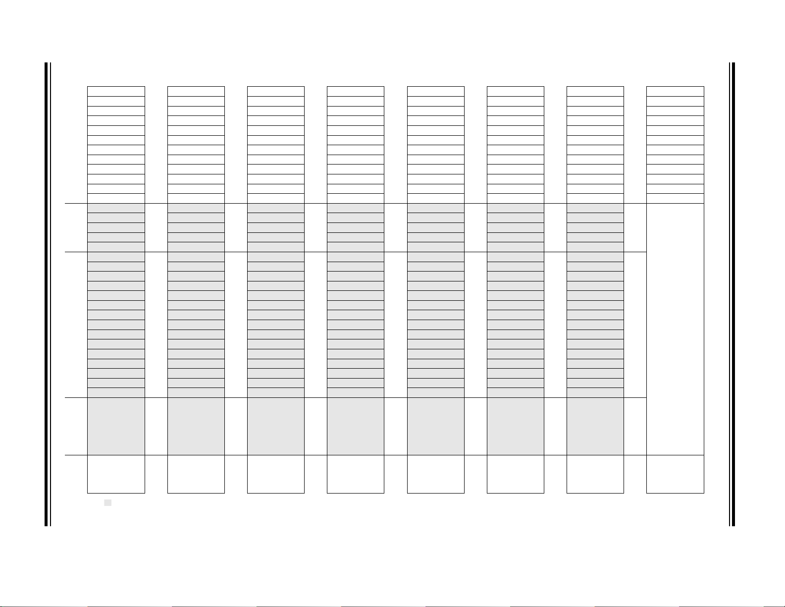
DS41414B-page 30 Preliminary 2010 Microchip Technology Inc.
Legend: = Unimplemented data memory locations, read as ‘0’.
BANK 24 BANK 25 BANK 26 BANK 27 BANK 28 BANK 29 BANK 30 BANK 31
C00h INDF0 C80h INDF0 D00h INDF0 D80h INDF0 E00h INDF0 E80h INDF0 F00h INDF0 F80h INDF0
C01h INDF1 C81h INDF1 D01h INDF1 D81h INDF1 E01h INDF1 E81h INDF1 F01h INDF1 F81h INDF1
C02h PCL C82h PCL D02h PCL D82h PCL E02h PCL E82h PCL F02h PCL F82h PCL
C03h STATUS C83h STATUS D03h STATUS D83h STATUS E03h STATUS E83h STATUS F03h STATUS F83h STATUS
C04h FSR0L C84h FSR0L D04h FSR0L D84h FSR0L E04h FSR0L E84h FSR0L F04h FSR0L F84h FSR0L
C05h FSR0H C85h FSR0H D05h FSR0H D85h FSR0H E05h FSR0H E85h FSR0H F05h FSR0H F85h FSR0H
C06h FSR1L C86h FSR1L D06h FSR1L D86h FSR1L E06h FSR1L E86h FSR1L F06h FSR1L F86h FSR1L
C07h FSR1H C87h FSR1H D07h FSR1H D87h FSR1H E07h FSR1H E87h FSR1H F07h FSR1H F87h FSR1H
C08h BSR C88h BSR D08h BSR D88h BSR E08h BSR E88h BSR F08h BSR F88h BSR
C09h WREG C89h WREG D09h WREG D89h WREG E09h WREG E89h WREG F09h WREG F89h WREG
C0Ah PCLATH C8Ah PCLATH D0Ah PCLATH D8Ah PCLATH E0Ah PCLATH E8Ah PCLATH F0Ah PCLATH F8Ah PCLATH
C0Bh INTCON C8Bh INTCON D0Bh INTCON D8Bh INTCON E0Bh INTCON E8Bh INTCON F0Bh INTCON F8Bh INTCON
C0Ch
—C8Ch—D0Ch—D8Ch—E0Ch—E8Ch—F0Ch—F8Ch
See Ta bl e 3 -8
C0Dh
—C8Dh—D0Dh—D8Dh—E0Dh—E8Dh—F0Dh—F8Dh
C0Eh
—C8Eh—D0Eh—D8Eh—E0Eh—E8Eh—F0Eh—F8Eh
C0Fh
—C8Fh—D0Fh—D8Fh—E0Fh—E8Fh—F0Fh—F8Fh
C10h
—C90h—D10h—D90h—E10h—E90h—F10h—F90h
C11h
—C91h—D11h—D91h—E11h—E91h—F11h—F91h
C12h
—C92h—D12h—D92h—E12h—E92h—F12h—F92h
C13h
—C93h—D13h—D93h—E13h—E93h—F13h—F93h
C14h
—C94h—D14h—D94h—E14h—E94h—F14h—F94h
C15h
—C95h—D15h—D95h—E15h—E95h—F15h—F95h
C16h
—C96h—D16h—D96h—E16h—E96h—F16h—F96h
C17h
—C97h—D17h—D97h—E17h—E97h—F17h—F97h
C18h
—C98h—D18h—D98h—E18h—E98h—F18h—F98h
C19h
—C99h—D19h—D99h—E19h—E99h—F19h—F99h
C1Ah
—C9Ah—D1Ah—D9Ah—E1Ah—E9Ah—F1Ah—F9Ah
C1Bh
—C9Bh—D1Bh—D9Bh—E1Bh—E9Bh—F1Bh—F9Bh
C1Ch
—C9Ch—D1Ch—D9Ch—E1Ch—E9Ch—F1Ch—F9Ch
C1Dh
—C9Dh—D1Dh—D9Dh—E1Dh—E9Dh—F1Dh—F9Dh
C1Eh
—C9Eh—D1Eh—D9Eh—E1Eh—E9Eh—F1Eh—F9Eh
C1Fh
—C9Fh—D1Fh—D9Fh—E1Fh—E9Fh—F1Fh—F9Fh
C20h
Unimplemented
Read as ‘0’
CA0h
Unimplemented
Read as ‘0’
D20h
Unimplemented
Read as ‘0’
DA0h
Unimplemented
Read as ‘0’
E20h
Unimplemented
Read as ‘0’
EA0h
Unimplemented
Read as ‘0’
F20h
Unimplemented
Read as ‘0’
FA0h
C6Fh CEFh D6Fh DEFh E6Fh EEFh F6Fh FEFh
C70h
Accesses
70h – 7Fh
CF0h
Accesses
70h – 7Fh
D70h
Accesses
70h – 7Fh
DF0h
Accesses
70h – 7Fh
E70h
Accesses
70h – 7Fh
EF0h
Accesses
70h – 7Fh
F70h
Accesses
70h – 7Fh
FF0h
Accesses
70h – 7Fh
CFFh
CFFh D7Fh DFFh E7Fh EFFh F7Fh FFFh
TABLE 3-6: PIC16F/LF1946/47 MEMORY MAP, BANKS 24-31
PIC16F/LF1946/47
 Loading...