


PIC16(L)F1704/8
14/20-Pin 8-Bit Advanced Analog Flash Microcontrollers
High-Performance RISC CPU:
• C Compiler Optimized Architecture
• Only 49 Instructions
• Up to 14 Kbytes Linear Program Memory
Addressing
• Operating Speed:
- DC – 32 MHz
- DC – 125 ns instruction cycle
• Interrupt Capability with Automatic Context
Saving
• 16-Level Deep Hardware Stack with Optional
Overflow/Underflow Reset
• Direct, Indirect and Relative Addressing modes:
- Two full 16-bit File Select Registers (FSRs)
- FSRs can read program and data memory
Flexible Oscillator Structure:
• 16 MHz Internal Oscillator Block:
- Accurate to ±1%, typical
- Software selectable frequency range from 16
MHz to 250 kHz
- PLL multiplier to 32 MHz
• 31 kHz Low-Power Internal Oscillator
• External Oscillator Block with:
- Three crystal/resonator modes up to 20 MHz
- Three external clock modes up to 20 MHz
• Fail-Safe Clock Monitor:
- Allows for safe shutdown if peripheral clock
stops
• Two-Speed Oscillator Start-up
• Oscillator Start-up Timer (OST)
Special Microcontroller Features:
• Operating Voltage Range:
- 1.8V-3.6V (PIC16LF1704/8)
- 2.3V-5.5V (PIC16F1704/8)
• Temperature Range:
- Industrial: -40°C to 85°C
- Extended: -40°C to 125°C
• Power-on Reset (POR)
• Low Power Brown-Out Reset (LPBOR)
• Extended Watch-Dog Timer (WDT):
- Programmable period from 1 ms to 256s
• Programmable Code Protection
• In-Circuit Serial Programming™ (ICSP™) via
Two Pins
• In-Circuit Debug (ICD) via Two Pins
• Enhanced Low-Voltage Programming (LVP)
• Power-Saving Sleep mode
Low-Power Features (PIC16LF1704/8):
• Standby Current:
- 30 nA @ 1.8V, typical
• Operating Current:
-35A/MHz, typical
• Low-Power Watchdog Timer Current:
- 300 nA @ 1.8V, typical
Digital Peripheral Features:
• Up to 17 I/O Pins and 1 Input-only Pin:
- High current sink/source for LED drivers
- Individually programmable weak pull-ups
- Interrupt-on-change pin option with edge
selectable option
• Timer0: 8-Bit Timer/Counter with 8-Bit
Programmable Prescaler
• Enhanced Timer1:
- 16-bit timer/counter with prescaler
- External Gate Input mode
- Dedicated low-power 32 kHz oscillator driver
• Timer2:
- Up to 3 (TMR2/4/6)
- 8-Bit Timer/Counter
- 8-Bit Period Register
- Prescaler and Postscaler
• Capture, Compare, PWM (CCP) Module
• Master Synchronous Serial Port (SSP) with SPI
2
CTM with:
and I
- 7-bit address masking
- SMBus/PMBusTM compatibility
• Enhanced Universal Synchronous Asynchronous
Receiver Transmitter (EUSART):
- RS-232, RS-485 and LIN compatible
- Auto-Baud Detect
- Auto-wake-up on Start
• Complementary Output Generator (COG):
- Push-Pull, Full Bridge, and Steering modes
- Dedicated Rise/Fall Input Triggers
- Dedicated Deadtime Delay Counters
- Dedicated Phase Delay Counters
- Dedicated Blanking Delay Counters
- Concurrent Auto-Shutdown Selection
• Two Pulse Width Modulation (PWM) modules:
- 10-bit Duty-Cycle Control
• Three Configurable Logic Cell (CLC) modules:
- Generate a selected function of up to 4 inputs
- Combinational and State Logic
- External or Internal input/output pins
- Operation in Sleep
2013 Microchip Technology Inc. Preliminary DS40001715B-page 1
PIC16(L)F1704/8
Digital Peripheral Features (Continued):
• Peripheral Pin Select (PPS):
- Digital outputs mapped to any GPIO pin
- Digital inputs from any GPIO pin
- CLC input multiplexing
• 8-Bit Digital-to-Analog Converter (DAC):
- Output available externally
- Positive and negative reference selection
- Internal connections to comparators, op
amps, Fixed Voltage Reference (FVR) and
ADC
• Zero-Cross Detection Circuit:
Analog Peripheral Features:
• Operational Amplifiers:
- Up to two Configurable Op Amps
- Selectable internal and external channels
- High/Low selectable Gain Bandwidth Product
• Two High-Speed Comparators:
- Constant Voltage Output
- Current Source/Sink
- Interrupt on Edge Detect
• Voltage Reference module:
- Fixed Voltage Reference (FVR) with 1.024V,
2.048V and 4.096V output levels
- 60 ns response time
- Low-power/High-power mode
- Comparator outputs externally accessible
- Software hysteresis enable
• Analog-to-Digital Converter (ADC) module
- 10-bit resolution, 12 channels
- Auto conversion start capability
- Conversion available during Sleep
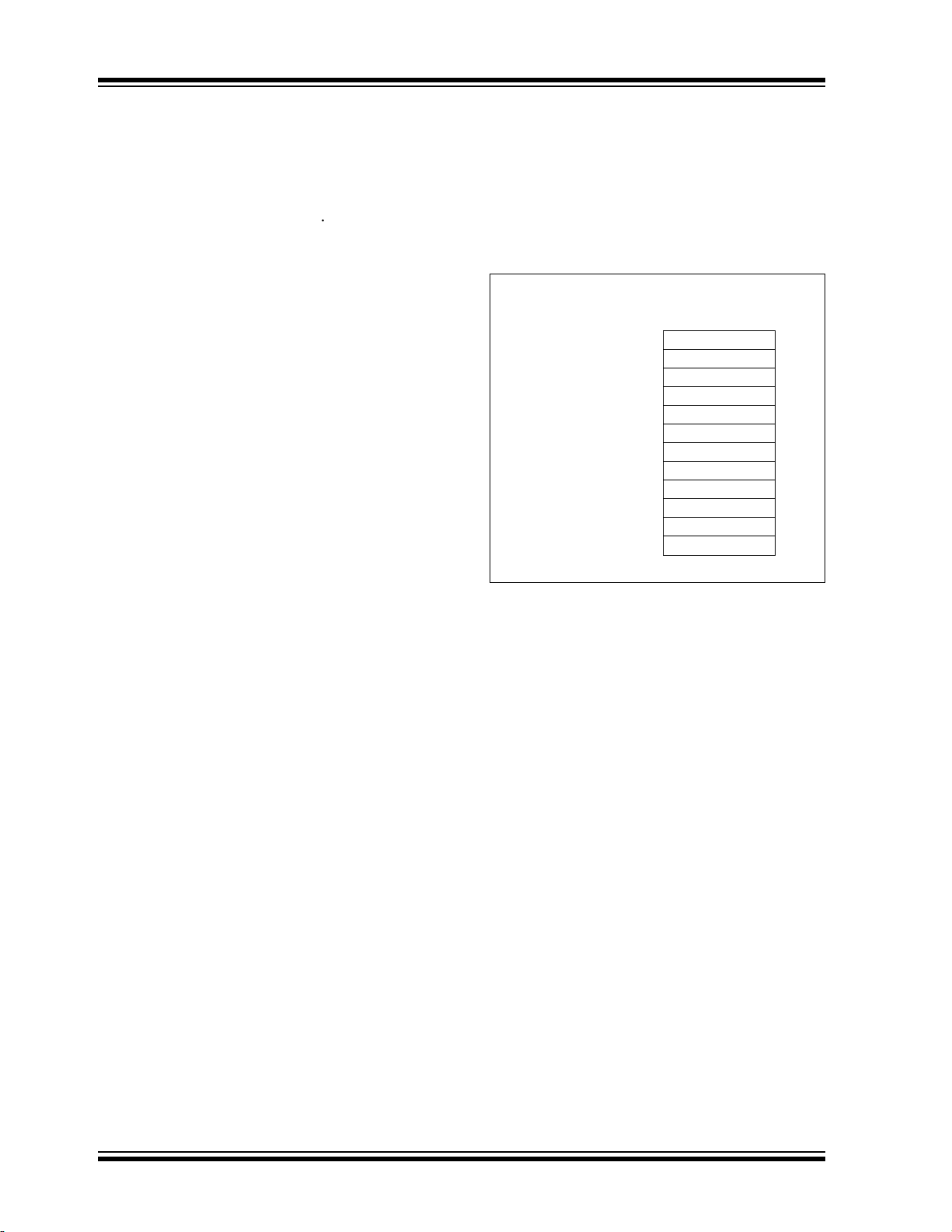
PIC16(L)F170x Family Types
(1)
PPS
XLP
Debug
Device
Flash (words)
Data Sheet Index
Program Memory
PIC16(L)F1703 (3) 2048 256 12 8 0 0 2 1 2/1 2 0 0 0 1 0 Y I/E Y
PIC16(L)F1704 (1) 4096 512 12 8 1 2 2 1 4/1 2 2 1 1 1 3 Y I/E Y
PIC16(L)F1705 (2) 8192 1024 12 8 1 2 2 1 4/1 2 2 1 1 1 3 Y I/E Y
PIC16(L)F1707 (3) 2048 256 18 12 0 0 2 1 2/1 2 0 0 0 1 0 Y I/E Y
PIC16(L)F1708 (1) 4096 512 18 12 1 2 2 1 4/1 221113YI/EY
PIC16(L)F1709 (2) 8192 1024 18 12 1 2 2 1 4/1 2 2 1 1 1 3 Y I/E Y
Note 1: Debugging Methods: (I) – Integrated on Chip; (H) – using Debug Header; E – using Emulation Header.
2: One pin is input-only.
Data Sheet Index: (Unshaded devices are described in this document.)
1: DS40001715 PIC16(L)F1704/8 Data Sheet, 14/20-Pin Flash, 8-bit Microcontrollers.
2: Future Release PIC16(L)F1705/9 Data Sheet, 14/20-Pin Flash, 8-bit Microcontrollers.
3: Future Release PIC16(L)F1703/7 Data Sheet, 14/20-Pin Flash, 8-bit Microcontrollers.
(bytes)
Data SRAM
(2)
I/O’s
8-bit DAC
10-bit ADC (ch)
Op Amp
High-Speed/
Comparators
Zero Cross
Timers
(8/16-bit)
CCP
COG
PWM
C™/SPI)
2
EUSART
CLC
MSSP (I
Note: For other small form-factor package availability and marking information, please visit
http://www.microchip.com/packaging or contact your local sales office.
DS40001715B-page 2 Preliminary 2013 Microchip Technology Inc.
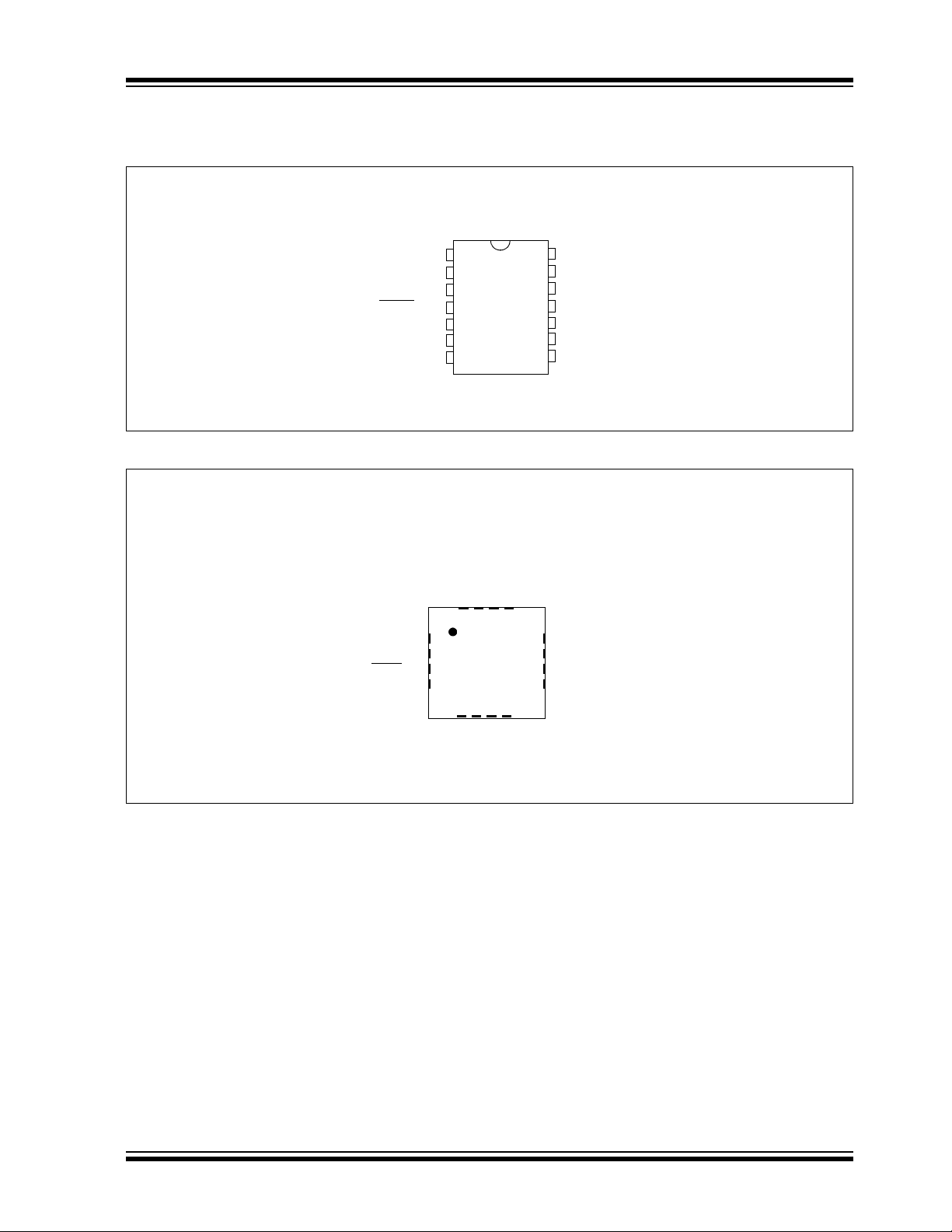
PIC16(L)F1704/8
PDIP, SOIC, TSSOP
PIC16(L)F1704
1
2
3
4
5
6
7
VDD
RA5
RA4
V
PP/MCLR/RA3
RC5
RC4
RC3
RA0/ICSPDAT
RA1/ICSPCLK
RA2
RC0
RC1
RC2
14
13
12
11
10
9
8
V
SS
2
3
1
9
10
11
12
RC4
4
VSS
RA0/ICSPDAT
RA1/ICSPCLK
RA2
RC0
NC
NC
V
DD
RA5
RA4
RA3/MCLR
/VPP
RC5
RC3
RC2
RC1
675
8
151416
13
PIC16(L)F1704
QFN
Pin Diagrams
FIGURE 1: 14-PIN DIAGRAM FOR PIC16(L)F1704
FIGURE 2: 16-PIN PACKAGE DIAGRAM FOR PIC16(L)F1704
2013 Microchip Technology Inc. Preliminary DS40001715B-page 3
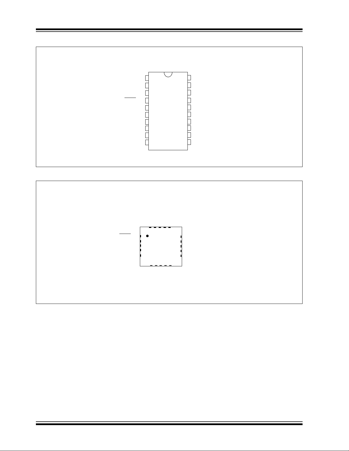
PIC16(L)F1704/8
PDIP, SOIC, SSOP
PIC16(L)F1708
2
3
4
5
6
7
8
9
10
VDD
RA5
RA4
V
PP/MCLR/RA3
RC5
RC4
RC3
RC6
RC7
RB7
ICSPDAT/RA0
ICSPCLK/RA1
RA2
RC0
RC1
RC2
RB4
RB5
RB6
20
19
18
17
16
15
14
13
12
11
VSS
1
QFN
2
3
4
5
1
678
9
20
191817
16
10
12
13
14
15
11
PIC16(L)F1708
RB4
RB5
RB6
RB7
RC7
VPP/MCLR/RA3
RC5
RC4
RC3
RC6
RA4
RA5
V
DD
VSS
RA0/ICSPDAT
RA1/ICSPCLK
RA2
RC0
RC1
RC2
FIGURE 3: 20-PIN PACKAGE DIAGRAM FOR PIC16(L)F1708
FIGURE 4: 20-PIN PACKAGE DIAGRAM FOR PIC16(L)F1708
DS40001715B-page 4 Preliminary 2013 Microchip Technology Inc.
2013 Microchip Technology Inc. Preliminary DS40001715B-page 5
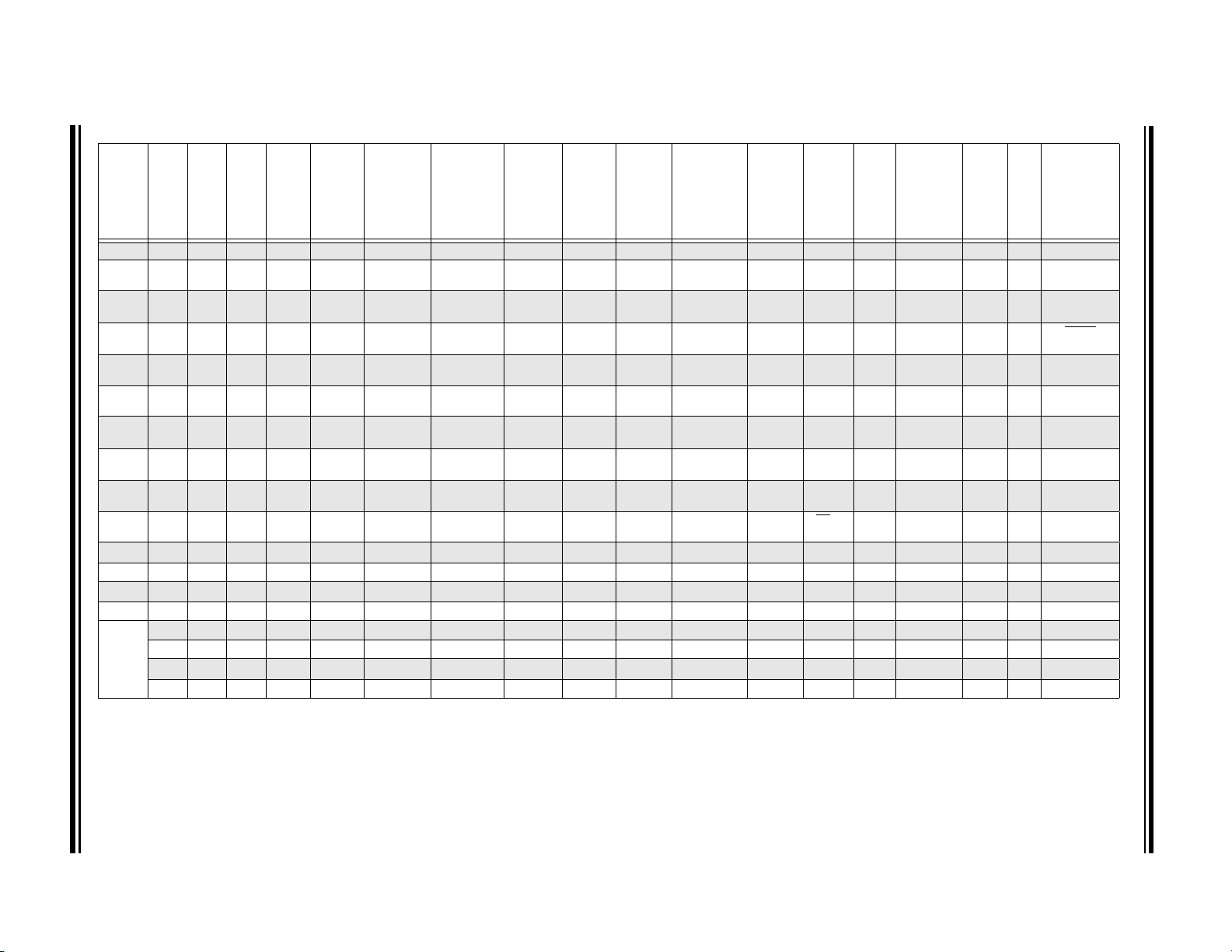
TABLE 1: 14/16-PIN ALLOCATION TABLE (PIC16(L)F1704)
(2)
I/O
QFN
ADC
Reference
Comparator
Op Amp
DAC
Zero Cross
Timers
CCP
PWM
COG
MSSP
EUSART
CLC
Pull-up
Interrupt
PDIP/SOIC/SSOP
RA0 13 12 AN0 VREF- C1IN+ — DAC1OUT — — — — — — — IOC Y ICSPDAT
RA1 12 11 AN1 VREF+ C1IN0-
————— ————IOC Y ICSPCLK
C2IN0-
RA2 11 10 AN2 — — — DAC1OUT2 ZCD T0CKI
(1)
— COGIN
(1)
— — — INT
(1)
Y —
IOC
RA3 4 3 — — — — — — —— ————IOC Y MCLR
RA4 3 2 AN3
— — — — —
RA5 2 1 — — —— — —T1CKI
(1)
T1G
SOSCO
— — — — —
(1)
————
CLCIN3
IOC Y CLKOUT
(1)
IOC Y CLKIN
SOSCI
RC0 10 9 AN4 — C2IN+
RC1 9 8 AN5 — C1IN1-
C2IN1-
RC2 8 7 AN6 — C1IN2-
C2IN2-
RC3 7 6 AN7 — C1IN3-
OPA1IN+ — — — — — SCK
OPA1IN- — — — — — SDI
OPA1OUT
OPA2OUT — — — CCP2
— — — — — — — —
(1)
—SS
SCL
SDA
(1)
(3)
(1)
(3)
(1)
— —
— CLCIN2
— CLCIN0
IOC Y —
(1)
IOC Y —
IOC Y —
(1)
IOC Y —
VPP
OSC2
OSC1
C2IN3-
RC4 6 5
— — — OPA2IN- — — — — — — CK
RC5 5 4 — — —OPA2IN+ — — — CCP1
VDD 1 16
— — — — — — — — — — — — — —
(1)
(1)
——RX
(1,3)
(1)
CLCIN1
IOC Y —
— IOC Y —
VDD
VSS 14 13 — — — — — — — — — — — — — — VSS
(3)
CK CLC1OUT — — —
(3)
(3)
DT
CLC2OUT — — —
OUT
— — — — C1OUT — — — — CPP1 PWM3OUT COGA SDA
— — — — C2OUT — — — — CPP2 PWM4OUT COGB SCL
(2)
— — — — — — — — — — — COGC SDO TX CLC3OUT — — —
————— — — ——— —COGDSCK—————
Note 1: Default peripheral input. Input can be moved to any other pin with the PPS input selection registers. See Register 12-1.
2: All pin outputs default to PORT latch data. Any pin can be selected as a digital peripheral output with the PPS output selection registers. See Register 12-3.
3: These peripheral functions are bidirectional. The output pin selections must be the same as the input pin selections.
Basic
PIC16(L)F1704/8
DS40001715B-page 6 Preliminary 2013 Microchip Technology Inc.
TABLE 2: 20-PIN ALLOCATION TABLE (PIC16(L)F1708)
PIC16(L)F1704/8
(2)
I/O
QFN
SSOP
PDIP/SOIC/
ADC
Reference
Comparator
Op Amp
DAC
Zero Cross
Timers
CCP
PWM
COG
MSSP
EUSART
CLC
Pull-up
Interrupt
RA0 19 16 AN0 VREF- C1IN+ — DAC1OUT — — — — — — — — IOC Y ICSPDAT
RA1 18 15 AN1 VREF+ C1IN0-
——————————IOC Y ICSPCLK
C2IN0-
RA2 17 14 AN2 — — — DAC1OUT2 ZCD T0CKI
(1)
— — COGIN
(1)
— — — INT
(1)
Y —
IOC
RA3 4 1 — — —— — ——— — ————IOC Y MCLR
VPP
RA4 3 20 AN3
— — — — —
RA5 2 19 — — —— — —T1CKI
RB4 13 10 AN10 — — OPA1IN-
— — — — — —
RB5 12 9 AN11 — — OPA1IN+ — — —— — ——RX
RB6 11 8
— — — — — — — — — —
RB7 10 7 — — —— — ——— — ——CK
RC0 16 13 AN4 — C2IN+
RC1 15 12 AN5 — C1IN1-
C2IN1-
RC2 14 11 AN6 — C1IN2-
C2IN2-
RC3 7 4 AN7 — C1IN3-
— — — — — — — — — —
—————————CLCIN2
OPA1OUT
— — — — — — — — —
OPA2OUT — — — CCP2
(1)
T1G
SOSCO
SOSCI
— — — — — —
—————CLCIN3
(1)
SCK
SDA
SDI
SCL
(1)
————CLCIN0
—
(3)
(1,3)
(1)
—
(3)
(1)
—
—
— IOC Y —
IOC Y CLKOUT
(1)
IOC Y CLKIN
IOC Y —
IOC Y —
IOC Y —
IOC Y —
(1)
IOC Y —
IOC Y —
(1)
IOC Y —
OSC2
OSC1
C2IN3-
RC4 6 3
— — — — — — — — — — — —
RC5 5 2 — — —— — —— CCP1
RC6 8 5 AN8
— — OPA2IN- — — — — — —
(1)
—————IOC Y —
(1)
SS
— —
CLCIN1
(1)
IOC Y —
IOC Y —
RC7 9 6 AN9 — —OPA2IN+ — — — — — — — — — IOC Y —
VDD 1 18
— — — — — — — — — — — — — — —
VDD
VSS 20 17 — — — — — — — — — — — — — — — VSS
(3)
CK CLC1OUT — — —
(3)
(3)
DT
CLC2OUT — — —
OUT
— — — — C1OUT — — — — CPP1 PWM3OUT COGA SDA
— — — — C2OUT — — — — CPP2 PWM4OUT COGB SCL
(2)
— — — — — — — — — — — COGC SDO TX CLC3OUT — — —
————— — — ——— —COGDSCK—————
Note 1: Default peripheral input. Input can be moved to any other pin with the PPS input selection registers. See Register 12-2.
2: All pin outputs default to PORT latch data. Any pin can be selected as a digital peripheral output with the PPS output selection registers. See Register 12-3.
3: These peripheral functions are bidirectional. The output pin selections must be the same as the input pin selections.
Basic

PIC16(L)F1704/8
Table of Contents
1.0 Device Overview .......................................................................................................................................................................... 9
2.0 Enhanced Mid-Range CPU ........................................................................................................................................................ 17
3.0 Memory Organization................................................................................................................................................................. 19
4.0 Device Configuration.................................................................................................................................................................. 49
5.0 Resets........................................................................................................................................................................................ 55
6.0 Oscillator Module (with Fail-Safe Clock Monitor) ....................................................................................................................... 63
7.0 Interrupts .................................................................................................................................................................................... 81
8.0 Power-Down Mode (Sleep) ........................................................................................................................................................ 95
9.0 Watchdog Timer (WDT) ............................................................................................................................................................. 99
10.0 Flash Program Memory Control ............................................................................................................................................... 105
11.0 I/O Ports ................................................................................................................................................................................... 121
12.0 Peripheral Pin Select (PPS) Module ........................................................................................................................................ 139
13.0 Interrupt-On-Change ................................................................................................................................................................ 147
14.0 Fixed Voltage Reference (FVR) .............................................................................................................................................. 153
15.0 Temperature Indicator Module ................................................................................................................................................. 157
16.0 Comparator Module.................................................................................................................................................................. 159
17.0 Pulse Width Modulation (PWM) ............................................................................................................................................... 169
18.0 Complementary Output Generator (COG) Module................................................................................................................... 175
19.0 Configurable Logic Cell (CLC).................................................................................................................................................. 207
20.0 Analog-to-Digital Converter (ADC) Module .............................................................................................................................. 223
21.0 Operational Amplifier (OPA) Modules ...................................................................................................................................... 237
22.0 8-Bit Digital-to-Analog Converter (DAC1) Module.................................................................................................................... 241
23.0 Zero Cross Detection (ZCD) Module........................................................................................................................................ 245
24.0 Timer0 Module ......................................................................................................................................................................... 249
25.0 Timer1 Module with Gate Control............................................................................................................................................. 253
26.0 Timer2/4/6 Module ................................................................................................................................................................... 265
27.0 Capture/Compare/PWM Modules ............................................................................................................................................ 271
28.0 Master Synchronous Serial Port (MSSP) Module .................................................................................................................... 281
29.0 Enhanced Universal Synchronous Asynchronous Receiver Transmitter (EUSART) ............................................................... 337
30.0 In-Circuit Serial Programming™ (ICSP™) ............................................................................................................................... 369
31.0 Instruction Set Summary.......................................................................................................................................................... 371
32.0 Electrical Specifications............................................................................................................................................................ 385
33.0 DC and AC Characteristics Graphs and Charts ....................................................................................................................... 419
34.0 Development Support............................................................................................................................................................... 435
35.0 Packaging Information.............................................................................................................................................................. 439
The Microchip Web Site..................................................................................................................................................................... 467
Customer Change Notification Service .............................................................................................................................................. 467
Customer Support .............................................................................................................................................................................. 467
Product Identification System ............................................................................................................................................................ 469
2013 Microchip Technology Inc. Preliminary DS40001715B-page 7

PIC16(L)F1704/8
TO OUR VALUED CUSTOMERS
It is our intention to provide our valued customers with the best documentation possible to ensure successful use of your Microchip
products. To this end, we will continue to improve our publications to better suit your needs. Our publications will be refined and
enhanced as new volumes and updates are introduced.
If you have any questions or comments regarding this publication, please contact the Marketing Communications Department via
E-mail at docerrors@microchip.com. We welcome your feedback.
Most Current Data Sheet
To obtain the most up-to-date version of this data sheet, please register at our Worldwide Web site at:
http://www.microchip.com
You can determine the version of a data sheet by examining its literature number found on the bottom outside corner of any page.
The last character of the literature number is the version number, (e.g., DS30000000A is version A of document DS30000000).
Errata
An errata sheet, describing minor operational differences from the data sheet and recommended workarounds, may exist for current
devices. As device/documentation issues become known to us, we will publish an errata sheet. The errata will specify the revision
of silicon and revision of document to which it applies.
To determine if an errata sheet exists for a particular device, please check with one of the following:
• Microchip’s Worldwide Web site; http://www.microchip.com
• Your local Microchip sales office (see last page)
When contacting a sales office, please specify which device, revision of silicon and data sheet (include literature number) you are
using.
Customer Notification System
Register on our web site at www.microchip.com to receive the most current information on all of our products.
DS40001715B-page 8 Preliminary 2013 Microchip Technology Inc.
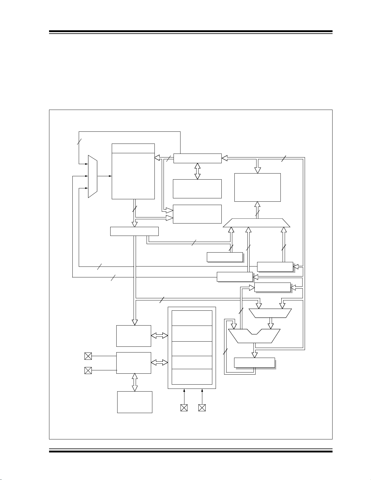
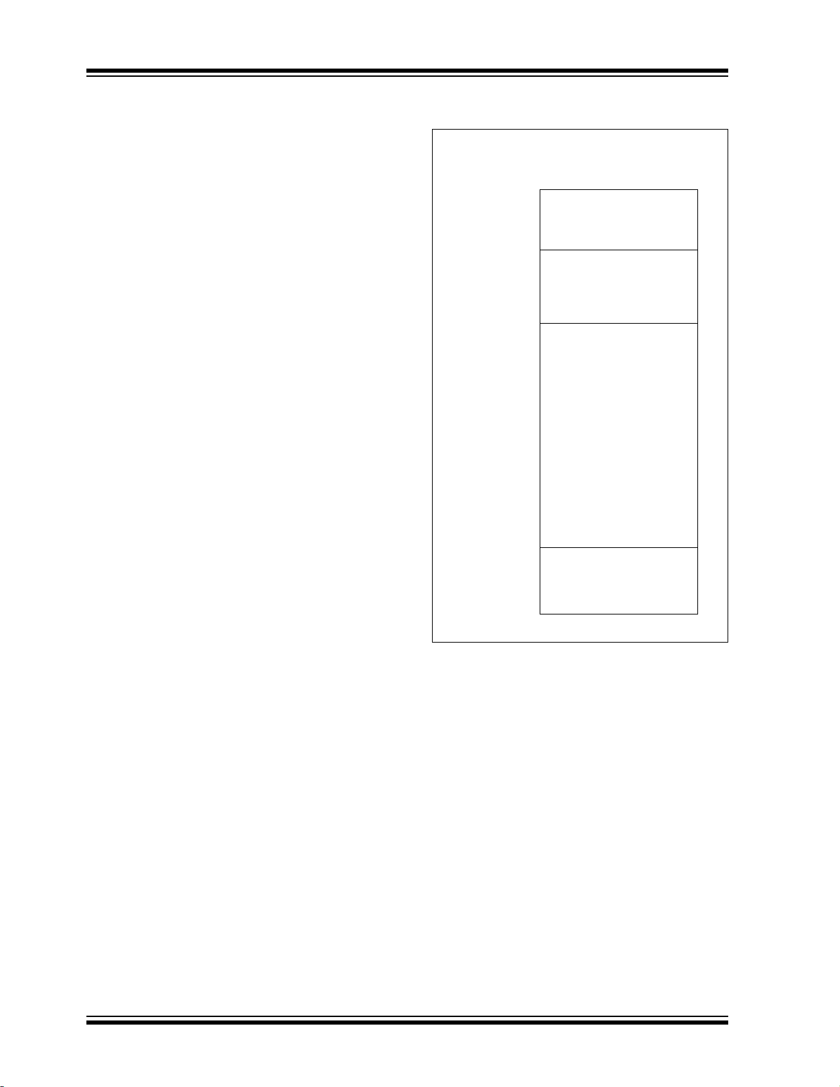
1.0 DEVICE OVERVIEW
The PIC16(L)F1704/8 are described within this data
sheet. They are available in 14-pin and 20-pin DIP
packages and 16-pin and 20-pin QFN packages.
Figure 1-1 shows a block diagram of the
PIC16(L)F1704/8 devices. Table 1-2 shows the pinout
descriptions.
Reference Table 1-1 for peripherals available per device.
TABLE 1-1: DEVICE PERIPHERAL
SUMMARY
Peripheral
PIC16(L)F1704
PIC16(L)F1708
Analog-to-Digital Converter (ADC) ●●
Digital-to-Analog Converter (DAC) ●●
Complementary Output Generator (COG) ●●
Fixed Voltage Reference (FVR) ●●
Zero Cross Detection (ZCD) ●●
Temperature Indicator ●●
Capture/Compare/PWM (CCP/ECCP) Modules
CCP1 ●●
CCP2 ●●
Comparators
C1 ●●
C2 ●●
Configurable Logic Cell (CLC)
CLC1 ●●
CLC2 ●●
CLC3 ●●
Enhanced Universal Synchronous/Asynchronous
Receiver/Transmitter (EUSART)
EUSART ●●
Master Synchronous Serial Ports
MSSP ●●
Op Amp
Op Amp 1 ●●
Op Amp 2 ●●
Pulse Width Modulator (PWM)
PWM3 ●●
PWM4 ●●
Timers
Timer0 ●●
Timer1 ●●
Timer2 ●●
PIC16(L)F1704/8
2013 Microchip Technology Inc. Preliminary DS40001715B-page 9
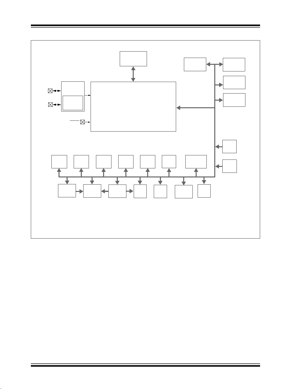
PIC16(L)F1704/8
PORTA
PORTB
(1)
PORTC
Note 1: PIC16(L)F1708 only.
2: See applicable chapters for more information on peripherals.
CPU
Program
Flash Memory
RAM
Timing
Generation
LFINTOSC
Oscillator
MCLR
Figure 1-1
CLKIN
CLKOUT
ADC
10-Bit
FVR
Te mp .
Indicator
EUSART
Comparators
MSSPTimer2Timer1Timer0
DAC
CCPs
PWMOp Amps
HFINTOSC/
CLCs
COG
ZCD
FIGURE 1-1: PIC16(L)F1704/8 BLOCK DIAGRAM
DS40001715B-page 10 Preliminary 2013 Microchip Technology Inc.
PIC16(L)F1704/8
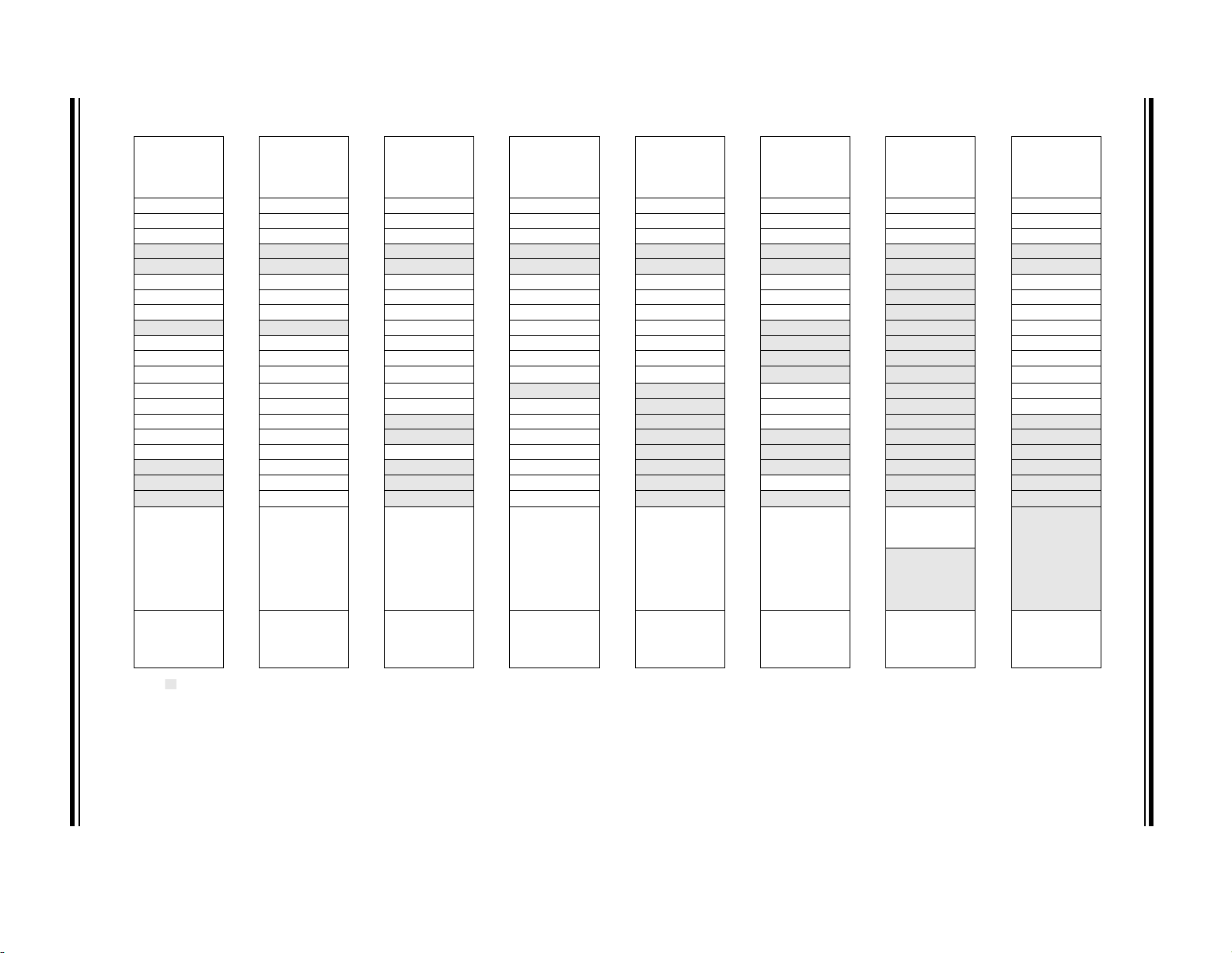
TABLE 1-2: PIC16(L)F1704 PINOUT DESCRIPTION
Input
Name Function
RA0/AN0/V
DAC1OUT/ICSPDAT
REF-/C1IN+/
RA0 TTL/ST CMOS General purpose I/O.
AN0 AN — ADC Channel 0 input.
REF- AN — ADC Negative Voltage Reference input.
V
C1IN+ AN — Comparator C1 positive input.
DAC1OUT — AN Digital-to-Analog Converter output.
ICSPDAT ST CMOS ICSP™ Data I/O.
RA1/AN1/V
ICSPCLK
REF+/C1IN0-/C2IN0-/
RA1 TTL/ST CMOS General purpose I/O.
AN1 AN — ADC Channel 1 input.
REF+ AN — ADC Voltage Reference input.
V
C1IN0- AN — Comparator C2 negative input.
C2IN0- AN — Comparator C3 negative input.
ICSPCLK ST — Serial Programming Clock.
RA2/AN2/DAC1OUT2/ZCD/
T0CKI
(1)
/COGIN
(1)
(1)
/INT
RA2 TTL/ST CMOS General purpose I/O.
AN2 AN — ADC Channel 2 input.
DAC1OUT2 — AN Digital-to-Analog Converter output.
ZCD — AN Zero Cross Detection Current Source/Sink.
T0CKI ST — Timer0 clock input.
COGIN ST CMOS Complementary Output Generator input.
INT ST — External interrupt.
RA3/MCLR
/VPP RA3 TTL/ST CMOS General purpose I/O.
MCLR
PP HV — Programming voltage.
V
RA4 TTL/ST CMOS General purpose I/O.
AN3 AN — ADC Channel 3 input.
RA4/AN3/T1G
OSC2/CLKOUT
(1)
/SOSCO/
T1G ST — Timer1 gate input.
SOSCO XTAL XTAL Secondary Oscillator Connection.
OSC2 — XTAL Crystal/Resonator (LP, XT, HS modes).
CLKOUT — CMOS F
RA5/T1CKI
(1)
CLCIN3
/SOSCI/
/OSC1/CLKIN
RA5 TTL/ST CMOS General purpose I/O.
T1CKI ST — Timer1 clock input.
(1)
SOSCI XTAL XTAL Secondary Oscillator Connection.
CLCIN3 ST — Configurable Logic Cell source input.
OSC1 — XTAL Crystal/Resonator (LP, XT, HS modes).
CLKIN ST — External clock input (EC mode).
RC0/AN4/C2IN+/OPA1IN+/
(1)
(3)
/SCL
SCK
RC0 TTL/ST CMOS General purpose I/O.
AN4 AN — ADC Channel 4 input.
C2IN+ AN — Comparator positive input.
OPA1IN+
SCK ST CMOS SPI clock.
SCL I
Legend: AN = Analog input or output CMOS = CMOS compatible input or output OD = Open Drain
TTL = TTL compatible input ST = Schmitt Trigger input with CMOS levels I
HV = High Voltage XTAL = Crystal levels
Note 1: Default peripheral input. Input can be moved to any other pin with the PPS input selection registers. See Register 12-1.
2: All pin outputs default to PORT latch data. Any pin can be selected as a digital peripheral output with the PPS output
selection registers. See Register 12-3.
3: These I
2
C functions are bidirectional. The output pin selections must be the same as the input pin selections.
Typ e
Output
Typ e
Description
ST — Master Clear with internal pull-up.
OSC/4 output.
AN —
2
CODI2C™ clock.
Operational Amplifier 1 non-inverting input.
2
C™ = Schmitt Trigger input with I2C
2013 Microchip Technology Inc. Preliminary DS40001715B-page 11
PIC16(L)F1704/8
TABLE 1-2: PIC16(L)F1704 PINOUT DESCRIPTION (CONTINUED)
Input
Name Function
RC1/AN5/C1IN1-/C2IN1-/
OPA1IN-/SDI
CLCIN2
(1)
(3)
/SDA
(1)
/
RC1 TTL/ST CMOS General purpose I/O.
AN5 AN — ADC Channel 5 input.
C1IN1-
C2IN1-
OPA1IN- AN — Operational Amplifier 1 inverting input.
SDI CMOS — SPI data input.
SDA I
CLCIN2 ST — Configurable Logic Cell source input.
RC2/AN6/C1IN2-/C2IN2-/
OPA1OUT
RC2 TTL/ST CMOS General purpose I/O.
AN6 AN — ADC Channel 6 input.
C1IN2- AN — Comparator C1 negative input.
C2IN2- AN — Comparator C2 negative input.
OPA1OUT
RC3/AN7/C1IN3-/C2IN3-/
OPA2OUT/CCP2
(1)
CLCIN0
(1)
(1)
/SS
/
RC3 TTL/ST CMOS General purpose I/O.
AN7 AN — ADC Channel 7 input.
C1IN3- AN — Comparator C1 negative input.
C2IN3- AN — Comparator C2 negative input.
OPA2OUT
CCP2 ST CMOS Capture/Compare/PWM2.
SS
CLCIN0 ST — Configurable Logic Cell source input.
RC4/OPA2IN-/CK
(1)
/CLCIN1
(1)
RC4 TTL/ST CMOS General purpose I/O.
OPA2IN- AN — Operational Amplifier 2 inverting input.
CK ST CMOS USART synchronous clock.
CLCIN1 ST — Configurable Logic Cell source input.
RC5/OPA2IN+/CCP1
/RX
RC5 TTL/ST CMOS General purpose I/O.
(1)
(1)
OPA2IN+ AN — Operational Amplifier 2 non-inverting input.
CCP1 ST CMOS Capture/Compare/PWM1.
RX ST — USART asynchronous input.
DD VDD Power — Positive supply.
V
SS VSS Power — Ground reference.
V
Legend: AN = Analog input or output CMOS = CMOS compatible input or output OD = Open Drain
TTL = TTL compatible input ST = Schmitt Trigger input with CMOS levels I
HV = High Voltage XTAL = Crystal levels
Note 1: Default peripheral input. Input can be moved to any other pin with the PPS input selection registers. See Register 12-1.
2: All pin outputs default to PORT latch data. Any pin can be selected as a digital peripheral output with the PPS output
selection registers. See Register 12-3.
3: These I
2
C functions are bidirectional. The output pin selections must be the same as the input pin selections.
Output
Typ e
Typ e
AN — Comparator C1 negative input.
AN — Comparator C2 negative input.
2
CODI2C™ data input/output.
—AN
—AN
Operational Amplifier 1 output.
Operational Amplifier 2 output.
Description
ST — Slave Select input.
2
C™ = Schmitt Trigger input with I2C
DS40001715B-page 12 Preliminary 2013 Microchip Technology Inc.
PIC16(L)F1704/8
TABLE 1-2: PIC16(L)F1704 PINOUT DESCRIPTION (CONTINUED)
Input
Name Function
(2)
OUT
Legend: AN = Analog input or output CMOS = CMOS compatible input or output OD = Open Drain
Note 1: Default peripheral input. Input can be moved to any other pin with the PPS input selection registers. See Register 12-1.
TTL = TTL compatible input ST = Schmitt Trigger input with CMOS levels I
HV = High Voltage XTAL = Crystal levels
2: All pin outputs default to PORT latch data. Any pin can be selected as a digital peripheral output with the PPS output
selection registers. See Register 12-3.
3: These I
2
C functions are bidirectional. The output pin selections must be the same as the input pin selections.
C1OUT — CMOS Comparator output.
C2OUT — CMOS Comparator output.
CCP1 — CMOS Capture/Compare/PWM1 output.
CCP2 — CMOS Capture/Compare/PWM2 output.
PWM3OUT — CMOS PWM3 output.
PWM4OUT — CMOS PWM4 output.
COGA — CMOS Complementary Output Generator Output A.
COGB — CMOS Complementary Output Generator Output B.
COGC — CMOS Complementary Output Generator Output C.
COGD — CMOS Complementary Output Generator Output D.
(3)
SDA
SDO — CMOS SPI data output.
SCK — CMOS SPI clock output.
(3)
SCL
TX/CK — CMOS USART asynchronous TX data/synchronous clock output.
DT — CMOS USART synchronous data output.
CLC1OUT — CMOS Configurable Logic Cell 1 source output.
CLC2OUT — CMOS Configurable Logic Cell 2 source output.
CLC3OUT — CMOS Configurable Logic Cell 3 source output.
Output
Typ e
Typ e
—ODI2C™ data input/output.
I2CODI2C™ clock output.
Description
2
C™ = Schmitt Trigger input with I2C
2013 Microchip Technology Inc. Preliminary DS40001715B-page 13
PIC16(L)F1704/8
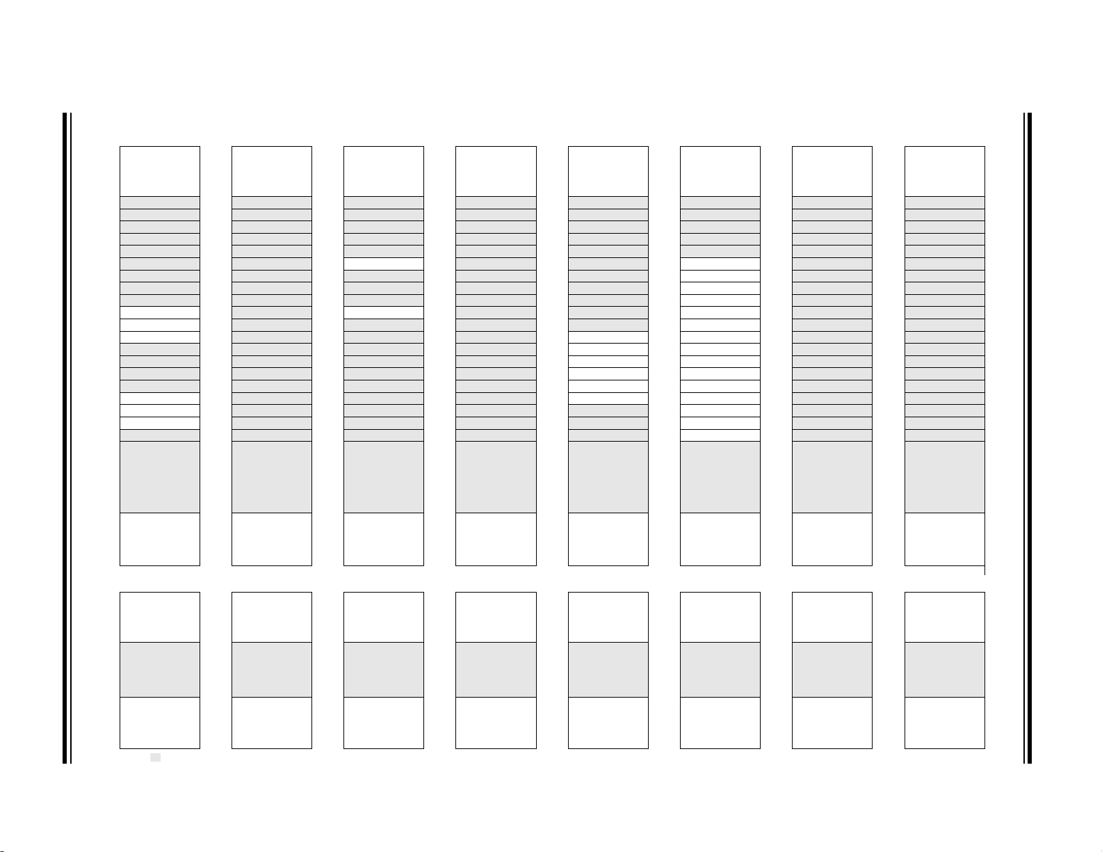
TABLE 1-3: PIC16(L)F1708 PIN OUT DESCRIPTION
Input
Name Function
RA0/AN0/V
DAC1OUT/ICSPDAT
REF-/C1IN+/
RA0 TTL/ST CMOS General purpose I/O.
AN0 AN — ADC Channel 0 input.
REF- AN — ADC Negative Voltage Reference input.
V
C1IN+ AN — Comparator C1 positive input.
DAC1OUT — AN Digital-to-Analog Converter output.
ICSPDAT ST CMOS ICSP™ Data I/O.
RA1/AN1/V
ICSPCLK
REF+/C1IN0-/C2IN0-/
RA1 TTL/ST CMOS General purpose I/O.
AN1 AN — ADC Channel 1 input.
REF+ AN — ADC Voltage Reference input.
V
C1IN0- AN — Comparator C2 negative input.
C2IN0- AN — Comparator C3 negative input.
ICSPCLK ST — Serial Programming Clock.
RA2/AN2/DAC1OUT2/ZCD/
T0CKI
(1)
/COGIN
(1)
(1)
/INT
RA2 TTL/ST CMOS General purpose I/O.
AN2 AN — ADC Channel 2 input.
DAC1OUT2 — AN Digital-to-Analog Converter output.
ZCD — AN Zero-Cross Detection Current Source/Sink.
T0CKI ST — Timer0 clock input.
COGIN ST CMOS Complementary Output Generator input.
INT ST — External interrupt.
RA3/MCLR
/VPP RA3 TTL/ST CMOS General purpose I/O.
MCLR
PP HV — Programming voltage.
V
RA4 TTL/ST CMOS General purpose I/O.
AN3 AN — ADC Channel 3 input.
RA4/AN3/T1G
OSC2/CLKOUT
(1)
/SOSCO/
T1G ST — Timer1 gate input.
SOSCO XTAL XTAL Secondary Oscillator Connection.
OSC2 — XTAL Crystal/Resonator (LP, XT, HS modes).
CLKOUT — CMOS F
RA5/T1CKI/SOSCI/
(1)
CLCIN3
/OSC1/CLKIN
RA5 TTL/ST CMOS General purpose I/O.
T1CKI ST — Timer1 clock input.
SOSCI XTAL XTAL Secondary Oscillator Connection.
CLCIN3 ST — Configurable Logic Cell source input.
OSC1 — XTAL Crystal/Resonator (LP, XT, HS modes).
CLKIN ST — External clock input (EC mode).
RB4/AN10/OPA1IN-/SCK
(3)
SDA
(1)
/
RB4 TTL/ST CMOS General purpose I/O.
AN10 AN — ADC Channel 10 input.
OPA1IN- AN — Operational Amplifier 1 inverting input.
SCK ST CMOS SPI clock.
SDA I
Legend: AN = Analog input or output CMOS = CMOS compatible input or output OD = Open Drain
TTL = TTL compatible input ST = Schmitt Trigger input with CMOS levels I
HV = High Voltage XTAL = Crystal levels
Note 1: Default peripheral input. Input can be moved to any other pin with the PPS input selection registers. See Register 12-2.
2: All pin outputs default to PORT latch data. Any pin can be selected as a digital peripheral output with the PPS output
selection registers. See Register 12-3.
3: These I
2
C functions are bidirectional. The output pin selections must be the same as the input pin selections.
Typ e
Output
Typ e
Description
ST — Master Clear with internal pull-up.
OSC/4 output.
2
CODI2C™ data input/output.
2
C™ = Schmitt Trigger input with I2C
DS40001715B-page 14 Preliminary 2013 Microchip Technology Inc.
PIC16(L)F1704/8
TABLE 1-3: PIC16(L)F1708 PIN OUT DESCRIPTION (CONTINUED)
Input
Name Function
RB5/AN11/OPA1IN+/RX
(1)
RB5 TTL/ST CMOS General purpose I/O.
AN11 AN — ADC Channel 11 input.
OPA1IN+ AN — Operational Amplifier 1 non-inverting input.
RX ST — USART asynchronous input.
RB6/SDI
/SCL
RB6 TTL/ST CMOS General purpose I/O.
(1)
(3)
SDI CMOS — SPI data input.
SCL I
(1)
RB7/CK
RB7 TTL/ST CMOS General purpose I/O.
CK ST CMOS USART synchronous clock.
RC0/AN4/C2IN+ RC0 TTL/ST CMOS General purpose I/O.
AN4 AN — ADC Channel 4 input.
C2IN+ AN — Comparator positive input.
RC1/AN5/C1IN1-/C2IN1-/
(1)
CLCIN2
RC1 TTL/ST CMOS General purpose I/O.
AN5 AN — ADC Channel 5 input.
C1IN1-
C2IN1-
CLCIN2 ST — Configurable Logic Cell source input.
RC2/AN6/C1IN2-/C2IN2-/
OPA1OUT
RC2 TTL/ST CMOS General purpose I/O.
AN6 AN — ADC Channel 6 input.
C1IN2- AN — Comparator C1 negative input.
C2IN2- AN — Comparator C2 negative input.
OPA1OUT
RC3/AN7/C1IN3-/C2IN3-/
OPA2OUT/CCP2
(1)
/CLCIN0
(1)
RC3 TTL/ST CMOS General purpose I/O.
AN7 AN — ADC Channel 7 input.
C1IN3- AN — Comparator C1 negative input.
C2IN3- AN — Comparator C2 negative input.
OPA2OUT
CCP2 ST CMOS Capture/Compare/PWM2.
CLCIN0 ST — Configurable Logic Cell source input.
RC4/CLCIN1
(1)
RC4 TTL/ST CMOS General purpose I/O.
CLCIN1 ST — Configurable Logic Cell source input.
RC5/CCP1
(1)
RC5 TTL/ST CMOS General purpose I/O.
CCP1 ST CMOS Capture/Compare/PWM1.
RC6/AN8/OPA2IN-/SS
(1)
RC6 TTL/ST CMOS General purpose I/O.
AN8 AN — ADC Channel 8 input.
OPA2IN- AN — Operational Amplifier 2 inverting input.
SS
RC7/AN9/OPA2IN+ RC7 TTL/ST CMOS General purpose I/O.
AN9 AN — ADC Channel 9 input.
OPA2IN+ AN — Operational Amplifier 2 non-inverting input.
DD VDD Power — Positive supply.
V
Legend: AN = Analog input or output CMOS = CMOS compatible input or output OD = Open Drain
TTL = TTL compatible input ST = Schmitt Trigger input with CMOS levels I
HV = High Voltage XTAL = Crystal levels
Note 1: Default peripheral input. Input can be moved to any other pin with the PPS input selection registers. See Register 12-2.
2: All pin outputs default to PORT latch data. Any pin can be selected as a digital peripheral output with the PPS output
selection registers. See Register 12-3.
3: These I
2
C functions are bidirectional. The output pin selections must be the same as the input pin selections.
Output
Typ e
Typ e
2
CODI2C™ clock.
AN — Comparator C1 negative input.
AN — Comparator C2 negative input.
—AN
—AN
Operational Amplifier 1 output.
Operational Amplifier 2 output.
Description
ST — Slave Select input.
2
C™ = Schmitt Trigger input with I2C
2013 Microchip Technology Inc. Preliminary DS40001715B-page 15
PIC16(L)F1704/8
TABLE 1-3: PIC16(L)F1708 PIN OUT DESCRIPTION (CONTINUED)
Input
Name Function
V
SS VSS Power — Ground reference.
(2)
OUT
Legend: AN = Analog input or output CMOS = CMOS compatible input or output OD = Open Drain
Note 1: Default peripheral input. Input can be moved to any other pin with the PPS input selection registers. See Register 12-2.
TTL = TTL compatible input ST = Schmitt Trigger input with CMOS levels I
HV = High Voltage XTAL = Crystal levels
2: All pin outputs default to PORT latch data. Any pin can be selected as a digital peripheral output with the PPS output
selection registers. See Register 12-3.
3: These I
2
C functions are bidirectional. The output pin selections must be the same as the input pin selections.
C1OUT — CMOS Comparator output.
C2OUT — CMOS Comparator output.
CCP1 — CMOS Capture/Compare/PWM1 output.
CCP2 — CMOS Capture/Compare/PWM2 output.
PWM3OUT — CMOS PWM3 output.
PWM4OUT — CMOS PWM4 output.
COGA — CMOS Complementary Output Generator Output A.
COGB — CMOS Complementary Output Generator Output B.
COGC — CMOS Complementary Output Generator Output C.
COGD — CMOS Complementary Output Generator Output D.
(3)
SDA
SDO — CMOS SPI data output.
SCK — CMOS SPI clock output.
(3)
SCL
TX/CK — CMOS USART asynchronous TX data/synchronous clock output.
DT — CMOS USART synchronous data output.
CLC1OUT — CMOS Configurable Logic Cell 1 source output.
CLC2OUT — CMOS Configurable Logic Cell 2 source output.
CLC3OUT — CMOS Configurable Logic Cell 3 source output.
Output
Typ e
Typ e
—ODI2C™ data input/output.
I2CODI2C™ clock output.
Description
2
C™ = Schmitt Trigger input with I2C
DS40001715B-page 16 Preliminary 2013 Microchip Technology Inc.
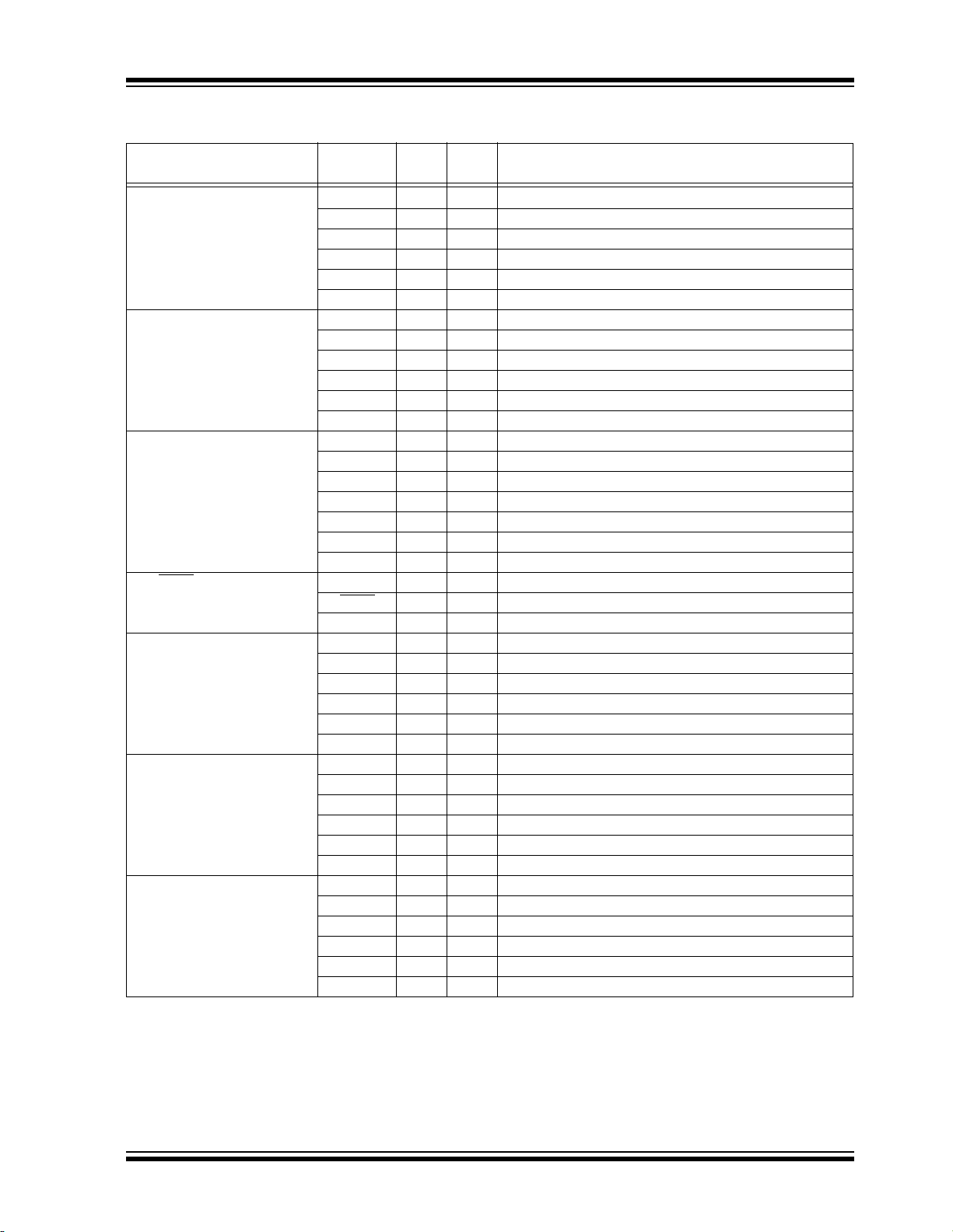
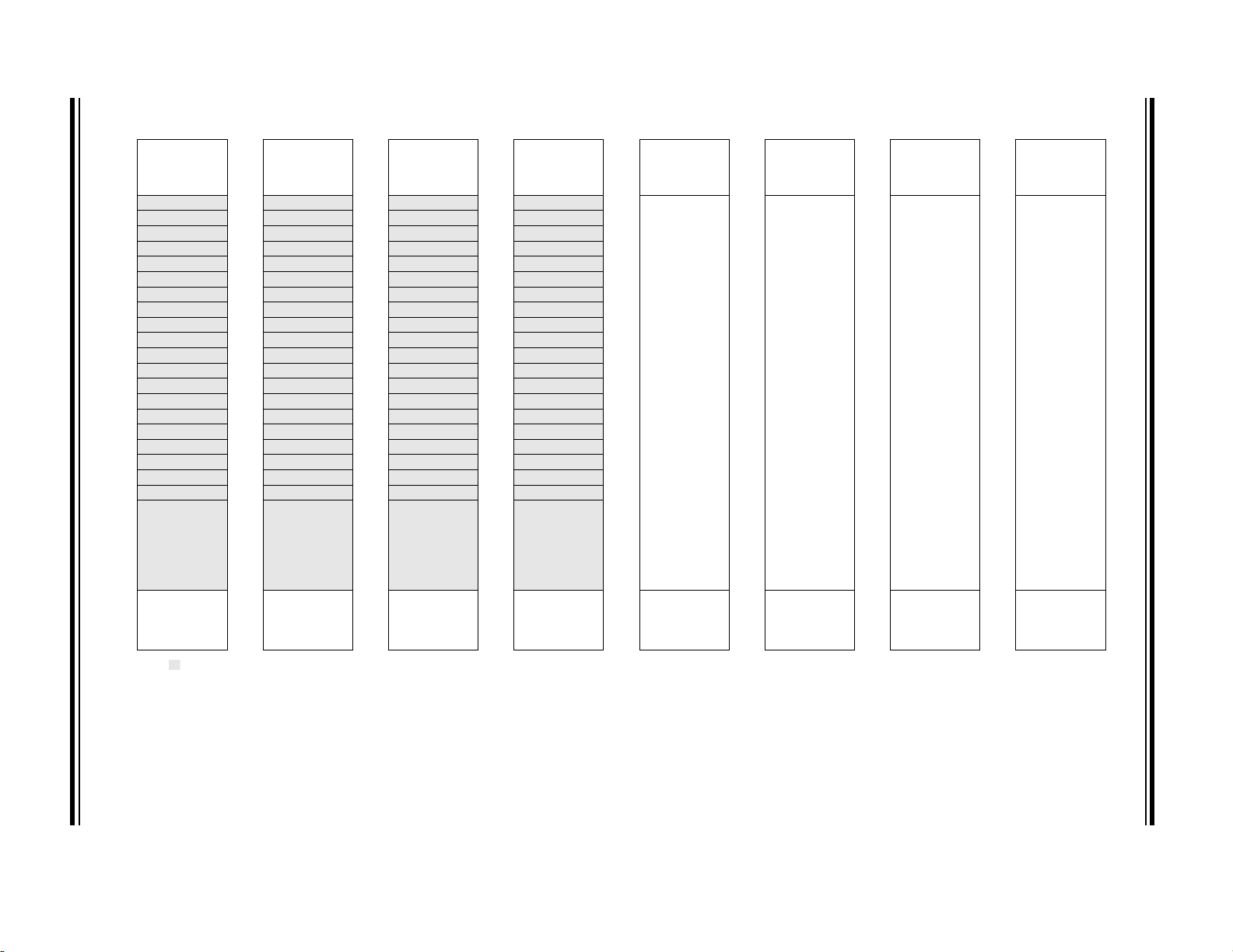
PIC16(L)F1704/8
Data Bus
8
14
Program
Bus
Instruction reg
Program Counter
8 Level Stack
(13-bit)
Direct Addr
7
12
Addr MUX
FSR reg
STATUS reg
MUX
ALU
Power-up
Timer
Oscillator
Start-up Timer
Power-on
Reset
Watchdog
Timer
Instruction
Decode &
Control
Timing
Generation
OSC1/CLKIN
OSC2/CLKOUT
V
DD
8
8
Brown-out
Reset
12
3
VSS
Internal
Oscillator
Block
Data Bus
8
14
Program
Bus
Instruction reg
Program Counter
8 Level Stack
(13-bit)
Direct Addr
7
Addr MUX
FSR reg
STATUS reg
MUX
ALU
W reg
Instruction
Decode &
Control
Timing
Generation
V
DD
8
8
3
VSS
Internal
Oscillator
Block
15
Data Bus
8
14
Program
Bus
Instruction Reg
Program Counter
16-Level Stack
(15-bit)
Direct Addr
7
RAM Addr
Addr MUX
Indirect
Addr
FSR0 Reg
STATUS Reg
MUX
ALU
Instruction
Decode and
Control
Timing
Generation
VDD
8
8
3
VSS
Internal
Oscillator
Block
RAM
FSR regFSR reg
FSR1 Reg
15
15
MUX
15
Program Memory
Read (PMR)
12
FSR regFSR reg
BSR Reg
5
ConfigurationConfigurationConfiguration
Flash
Program
Memory
2.0 ENHANCED MID-RANGE CPU
This family of devices contain an enhanced mid-range
8-bit CPU core. The CPU has 49 instructions. Interrupt
capability includes automatic context saving. The
hardware stack is 16 levels deep and has Overflow and
Underflow Reset capability. Direct, Indirect, and
FIGURE 2-1: CORE BLOCK DIAGRAM
Relative addressing modes are available. Two File
Select Registers (FSRs) provide the ability to read
program and data memory.
• Automatic Interrupt Context Saving
• 16-level Stack with Overflow and Underflow
• File Select Registers
• Instruction Set
2013 Microchip Technology Inc. Preliminary DS40001715B-page 17

PIC16(L)F1704/8
2.1 Automatic Interrupt Context Saving
During interrupts, certain registers are automatically
saved in shadow registers and restored when returning
from the interrupt. This saves stack space and user
code. See Section 7.5 “Automatic Context Saving”
for more information.
2.2 16-Level Stack with Overflow and Underflow
These devices have a hardware stack memory 15 bits
wide and 16 words deep. A Stack Overflow or Underflow will set the appropriate bit (STKOVF or STKUNF)
in the PCON register, and if enabled, will cause a software Reset. See Section 3.5 “Stack” for more details.
2.3 File Select Registers
There are two 16-bit File Select Registers (FSR). FSRs
can access all file registers and program memory,
which allows one Data Pointer for all memory. When an
FSR points to program memory, there is one additional
instruction cycle in instructions using INDF to allow the
data to be fetched. General purpose memory can now
also be addressed linearly, providing the ability to
access contiguous data larger than 80 bytes. There are
also new instructions to support the FSRs. See
Section 3.6 “Indirect Addressing” for more details.
2.4 Instruction Set
There are 49 instructions for the enhanced mid-range
CPU to support the features of the CPU. See
Section 31.0 “Instruction Set Summary” for more
details.
DS40001715B-page 18 Preliminary 2013 Microchip Technology Inc.
PIC16(L)F1704/8
3.0 MEMORY ORGANIZATION
These devices contain the following types of memory:
• Program Memory
- Configuration Words
- Device ID
-User ID
- Flash Program Memory
• Data Memory
- Core Registers
- Special Function Registers
- General Purpose RAM
- Common RAM
Note 1: The method to access Flash memory
through the PMCON registers is described
in Section 10.0 “Flash Program Memory
Control”.
The following features are associated with access and
control of program memory and data memory:
• PCL and PCLATH
•Stack
• Indirect Addressing
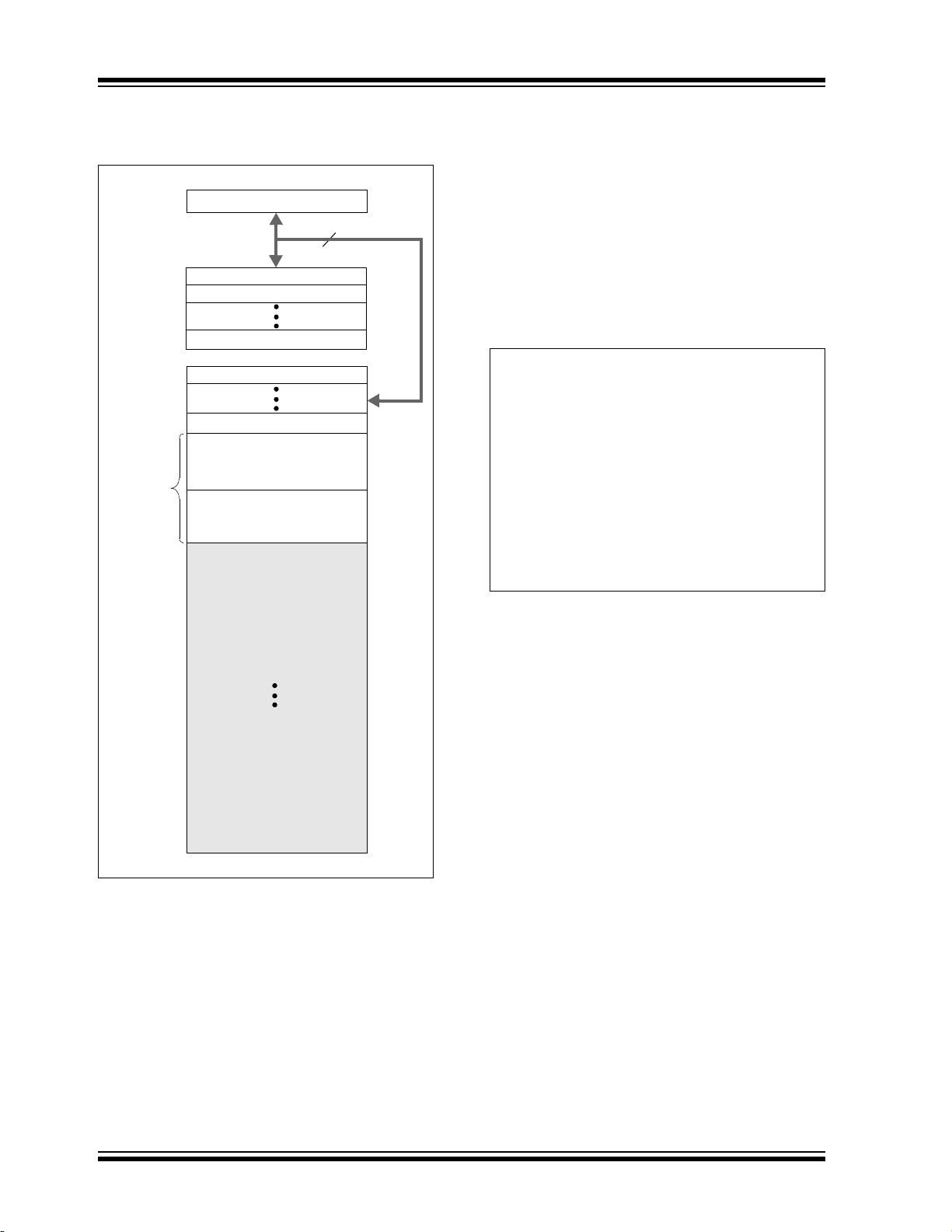
3.1 Program Memory Organization
The enhanced mid-range core has a 15-bit program
counter capable of addressing a 32K x 14 program
memory space. Table 3-1 shows the memory sizes
implemented for the PIC16(L)F1704/8 family. Accessing
a location above these boundaries will cause a
wrap-around within the implemented memory space.
The Reset vector is at 0000h and the interrupt vector is
at 0004h (see Figure 3-1).
TABLE 3-1: DEVICE SIZES AND ADDRESSES
Device Program Memory Space (Words) Last Program Memory Address
PIC16(L)F1704/8 4,096 0FFFh
2013 Microchip Technology Inc. Preliminary DS40001715B-page 19
PIC16(L)F1704/8
PC<14:0>
15
0000h
0004h
Stack Lev el 0
Stack Level 15
Reset Vector
Interrupt Vector
CALL, CALLW
RETURN, RETLW
Stack Lev el 1
0005h
On-chip
Program
Memory
Page 0
07FFh
Rollover to Page 0
0800h
0FFFh
1000h
7FFFh
Page 1
Rollover to Page 1
Interrupt, RETFIE
constants
BRW ;Add Index in W to
;program counter to
;select data
RETLW DATA0 ;Index0 data
RETLW DATA1 ;Index1 data
RETLW DATA2
RETLW DATA3
my_function
;… LOTS OF CODE…
MOVLW DATA_INDEX
call constants
;… THE CONSTANT IS IN W
FIGURE 3-1: PROGRAM MEMORY MAP
AND STACK FOR
PIC16(L)F1704/8
3.1.1 READING PROGRAM MEMORY AS DATA
There are two methods of accessing constants in
program memory. The first method is to use tables of
RETLW instructions. The second method is to set an
FSR to point to the program memory.
3.1.1.1 RETLW Instruction
The RETLW instruction can be used to provide access
to tables of constants. The recommended way to
create such a table is shown in Example 3-1.
EXAMPLE 3-1: RETLW INSTRUCTION
The BRW instruction makes this type of table very
simple to implement. If your code must remain portable
with previous generations of microcontrollers, then the
BRW instruction is not available so the older table read
method must be used.
3.1.1.2 Indirect Read with FSR
The program memory can be accessed as data by
setting bit 7 of the FSRxH register and reading the
matching INDFx register. The MOVIW instruction will
place the lower eight bits of the addressed word in the
W register. Writes to the program memory cannot be
performed via the INDF registers. Instructions that
access the program memory via the FSR require one
extra instruction cycle to complete. Example 3-2
demonstrates accessing the program memory via an
FSR.
The high directive will set bit<7> if a label points to a
location in program memory.
DS40001715B-page 20 Preliminary 2013 Microchip Technology Inc.

EXAMPLE 3-2: ACCESSING PROGRAM
constants
RETLW DATA0 ;Index0 data
RETLW DATA1 ;Index1 data
RETLW DATA2
RETLW DATA3
my_function
;… LOTS OF CODE…
MOVLW LOW constants
MOVWF FSR1L
MOVLW HIGH constants
MOVWF FSR1H
MOVIW 0[FSR1]
;THE PROGRAM MEMORY IS IN W
MEMORY VIA FSR
PIC16(L)F1704/8
2013 Microchip Technology Inc. Preliminary DS40001715B-page 21
PIC16(L)F1704/8
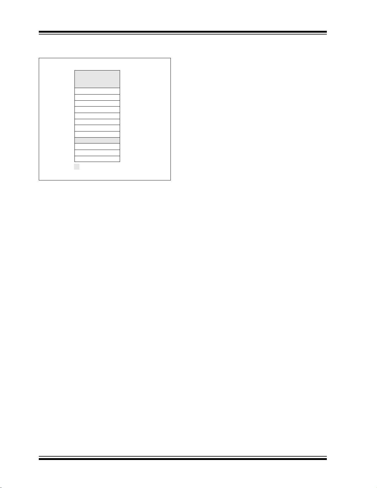
Addresses BANKx
x00h or x80h INDF0
x01h or x81h INDF1
x02h or x82h PCL
x03h or x83h STATUS
x04h or x84h FSR0L
x05h or x85h FSR0H
x06h or x86h FSR1L
x07h or x87h FSR1H
x08h or x88h BSR
x09h or x89h WREG
x0Ah or x8Ah PCLATH
x0Bh or x8Bh INTCON
3.2 Data Memory Organization
The data memory is partitioned in 32 memory banks
with 128 bytes in a bank. Each bank consists of
(Figure 3-2):
• 12 core registers
• 20 Special Function Registers (SFR)
• Up to 80 bytes of General Purpose RAM (GPR)
• 16 bytes of common RAM
The active bank is selected by writing the bank number
into the Bank Select Register (BSR). Unimplemented
memory will read as ‘0’. All data memory can be
accessed either directly (via instructions that use the
file registers) or indirectly via the two File Select
Registers (FSR). See Section 3.6 “Indirect
Addressing” for more information.
Data memory uses a 12-bit address. The upper five bits
of the address define the Bank address and the lower
seven bits select the registers/RAM in that bank.
3.2.1 CORE REGISTERS
The core registers contain the registers that directly
affect the basic operation. The core registers occupy
the first 12 addresses of every data memory bank
(addresses x00h/x08h through x0Bh/x8Bh). These
registers are listed below in Ta b l e 3 -2 . For detailed
information, see Tab le 3- 9.
TABLE 3-2: CORE REGISTERS
DS40001715B-page 22 Preliminary 2013 Microchip Technology Inc.
PIC16(L)F1704/8
3.2.1.1 STATUS Register
The STATUS register, shown in Register 3-1, contains:
• the arithmetic status of the ALU
• the Reset status
The STATUS register can be the destination for any
instruction, like any other register. If the STATUS
register is the destination for an instruction that affects
the Z, DC or C bits, then the write to these three bits is
disabled. These bits are set or cleared according to the
device logic. Furthermore, the TO
writable. Therefore, the result of an instruction with the
STATUS register as destination may be different than
intended.
and PD bits are not
For example, CLRF STATUS will clear the upper three
bits and set the Z bit. This leaves the STATUS register
as ‘000u u1uu’ (where u = unchanged).
It is recommended, therefore, that only BCF, BSF,
SWAPF and MOVWF instructions are used to alter the
STATUS register, because these instructions do not
affect any Status bits. For other instructions not
affecting any Status bits (Refer to Section 31.0
“Instruction Set Summary”).
Note: The C and DC bits operate as Borrow and
Digit Borrow
subtraction.
out bits, respectively, in
3.3 Register Definitions: Status
REGISTER 3-1: STATUS: STATUS REGISTER
U-0 U-0 U-0 R-1/q R-1/q R/W-0/u R/W-0/u R/W-0/u
— — —TOPD ZDC
bit 7 bit 0
Legend:
R = Readable bit W = Writable bit U = Unimplemented bit, read as ‘0’
u = Bit is unchanged x = Bit is unknown -n/n = Value at POR and BOR/Value at all other Resets
‘1’ = Bit is set ‘0’ = Bit is cleared q = Value depends on condition
(1)
(1)
C
bit 7-5 Unimplemented: Read as ‘0’
bit 4 TO
bit 3 PD
bit 2 Z: Zero bit
bit 1 DC: Digit Carry/Digit Borrow
bit 0 C: Carry/Borrow
Note 1: For Borrow, the polarity is reversed. A subtraction is executed by adding the two’s complement of the
second operand.
: Time-Out bit
1 = After power-up, CLRWDT instruction or SLEEP instruction
0 = A WDT Time-out occurred
: Power-Down bit
1 = After power-up or by the CLRWDT instruction
0 = By execution of the SLEEP instruction
1 = The result of an arithmetic or logic operation is zero
0 = The result of an arithmetic or logic operation is not zero
bit (ADDWF, ADDLW, SUBLW, SUBWF instructions)
1 = A carry-out from the 4th low-order bit of the result occurred
0 = No carry-out from the 4th low-order bit of the result
(1)
bit
(ADDWF, ADDLW, SUBLW, SUBWF instructions)
1 = A carry-out from the Most Significant bit of the result occurred
0 = No carry-out from the Most Significant bit of the result occurred
(1)
(1)
2013 Microchip Technology Inc. Preliminary DS40001715B-page 23
PIC16(L)F1704/8
0Bh
0Ch
1Fh
20h
6Fh
70h
7Fh
00h
Common RAM
(16 bytes)
General Purpose RAM
(80 bytes maximum)
Core Registers
(12 bytes)
Special Function Registers
(20 bytes maximum)
Memory Region
7-bit Bank Offset
3.3.1 SPECIAL FUNCTION REGISTER
The Special Function Registers are registers used by
the application to control the desired operation of
peripheral functions in the device. The Special Function
Registers occupy the 20 bytes after the core registers of
every data memory bank (addresses x0Ch/x8Ch
through x1Fh/x9Fh). The registers associated with the
operation of the peripherals are described in the
appropriate peripheral chapter of this data sheet.
3.3.2 GENERAL PURPOSE RAM
There are up to 80 bytes of GPR in each data memory
bank. The Special Function Registers occupy the 20
bytes after the core registers of every data memory
bank (addresses x0Ch/x8Ch through x1Fh/x9Fh).
3.3.2.1 Linear Access to GPR
The general purpose RAM can be accessed in a
non-banked method via the FSRs. This can simplify
access to large memory structures. See Section 3.6.2
“Linear Data Memory” for more information.
3.3.3 COMMON RAM
There are 16 bytes of common RAM accessible from all
banks.
FIGURE 3-2: BANKED MEMORY
PARTITIONING
DS40001715B-page 24 Preliminary 2013 Microchip Technology Inc.
3.3.4 DEVICE MEMORY MAPS
The memory maps for the device family are as shown
in Tables 3-3 through 3-8.
2013 Microchip Technology Inc. Preliminary DS40001715B-page 25
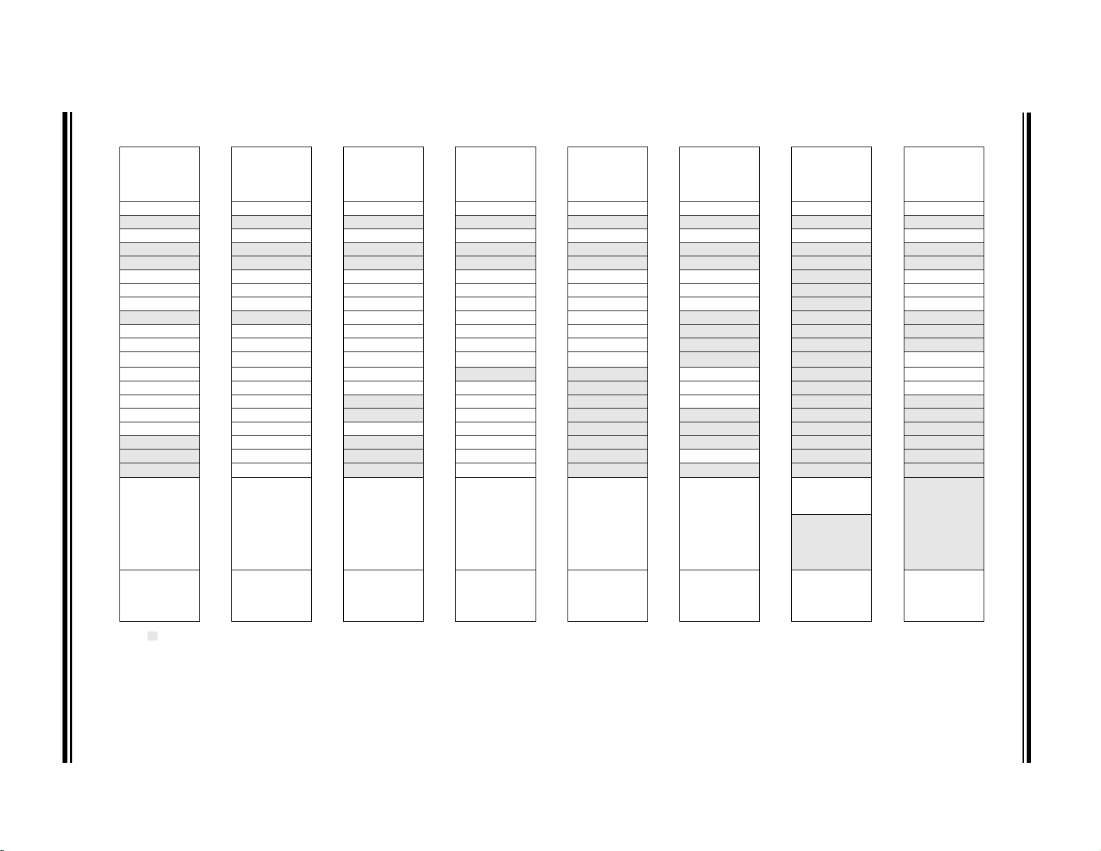
TABLE 3-3: PIC16(L)F1704 MEMORY MAP (BANKS 0-7)
BANK 0 BANK 1 BANK 2 BANK 3 BANK 4 BANK 5 BANK 6 BANK 7
000h
Core Registers
(Ta bl e 3- 2 )
00Bh 08Bh 10Bh 18Bh 20Bh 28Bh 30Bh 38Bh
00Ch PORTA 08Ch TRISA 10Ch LATA 18Ch ANSELA 20Ch WPUA 28Ch ODCONA 30Ch SLRCONA 38Ch INLVLA
00Dh
00Eh PORTC 08Eh TRISC 10Eh LATC 18Eh ANSELC 20Eh WPUC 28Eh ODCONC 30Eh SLRCONC 38Eh INLVLC
00Fh
010h
011h PIR1 091h PIE1 111h CM1CON0 191h PMADRL 211h SSP1BUF 291h CCPR1L 311h
012h PIR2 092h PIE2 112h CM1CON1 192h PMADRH 212h SSP1ADD 292h CCPR1H 312h
013h PIR3 093h PIE3 113h CM2CON0 193h PMDATL 213h SSP1MSK 293h CCP1CON 313h
014h
015h TMR0 095h OPTION_REG 115h CMOUT 195h PMCON1 215h SSP1CON 295h
016h TMR1L 096h PCON 116h BORCON 196h PMCON2 216h SSP1CON2 296h
017h TMR1H 097h WDTCON 117h FVRCON 197h VREGCON
018h T1CON 098h OSCTUNE 118h DAC1CON0 198h
019h T1GCON 099h OSCCON 119h DAC1CON1 199h RC1REG 219h
01Ah TMR2 09Ah OSCSTAT 11Ah
01Bh PR2 09Bh ADRESL 11Bh
01Ch T2CON 09Ch ADRESH 11Ch ZCD1CON 19Ch SP1BRGH 21Ch
01Dh
01Eh
01Fh
020h
06Fh 0EFh 16Fh 1EFh 26Fh 2EFh
070h
07Fh 0FFh 17Fh 1FFh 27Fh 2FFh 37Fh 3FFh
Legend: = Unimplemented data memory locations, read as ‘0’.
Note 1: Unimplemented on PIC16LF1704.
— 08Dh — 10Dh — 18Dh — 20Dh — 28Dh — 30Dh — 38Dh —
—08Fh—10Fh—18Fh—20Fh—28Fh—30Fh—38Fh—
—090h—110h—190h—210h—290h— 310h — 390h —
—094h— 114h CM2CON1 194h PMDATH 214h SSP1STAT 294h — 314h — 394h —
— 09Dh ADCON0 11Dh — 19Dh RC1STA 21Dh — 29Dh — 31Dh — 39Dh —
— 09Eh ADCON1 11Eh — 19Eh TX1STA 21Eh — 29Eh CCPTMRS 31Eh —39Eh—
— 09Fh ADCON2 11Fh — 19Fh BAUD1CON 21Fh —29Fh—31Fh—39Fh—
General
Purpose
Register
80 Bytes
Common RAM
70h – 7Fh
080h
0A0h
0F0h
Core Registers
(Ta bl e 3- 2 )
General
Purpose
Register
80 Bytes
Accesses
70h – 7Fh
100h
120h
170h
Core Registers
(Table 3-2)
— 19Ah TX1REG 21Ah — 29Ah CCP2CON 31Ah —39Ah—
— 19Bh SP1BRGL 21Bh —29Bh—31Bh—39Bh—
General
Purpose
Register
80 Bytes
Accesses
70h – 7Fh
180h
1A0h
1F0h
Core Registers
(Table 3-2)
—218h— 298h CCPR2L 318h — 398h IOCCN
General
Purpose
Register
80 Bytes
Accesses
70h – 7Fh
200h
Core Registers
(Table 3-2)
(1)
217h SSP1CON3 297h — 317h — 397h IOCCP
— 299h CCPR2H 319h — 399h IOCCF
— 29Ch — 31Ch — 39Ch —
220h
General
Purpose
Register
80 Bytes
270h
Accesses
70h – 7Fh
280h
2A0h
2F0h
Core Registers
(Table 3-2)
— 315h — 395h —
— 316h — 396h —
General
Purpose
Register
80 Bytes
Accesses
70h – 7Fh
300h
Core Registers
(Table 3-2)
— 391h IOCAP
— 392h IOCAN
— 393h IOCAF
320h
General Purpose
32Fh
330h
36Fh 3EFh
370h
Register
16 Bytes
Unimplemented
Read as ‘0’
Accesses
70h – 7Fh
380h
3A0h
3F0h
Core Registers
(Table 3-2)
Unimplemented
Read as ‘0’
Accesses
70h – 7Fh
PIC16(L)F1704/8
DS40001715B-page 26 Preliminary 2013 Microchip Technology Inc.
TABLE 3-4: PIC16(L)1708 MEMORY MAP (BANKS 0-7)
PIC16(L)F1704/8
BANK 0 BANK 1 BANK 2 BANK 3 BANK 4 BANK 5 BANK 6 BANK 7
000h
Core Registers
(Ta bl e 3- 2 )
00Bh 08Bh 10Bh 18Bh 20Bh 28Bh 30Bh 38Bh
00Ch PORTA 08Ch TRISA 10Ch LATA 18Ch ANSELA 20Ch WPUA 28Ch ODCONA 30Ch SLRCONA 38Ch INLVLA
00Dh PORTB 08Dh TRISB 10Dh LATB 18Dh ANSELB 20Dh WPUB 28Dh ODCONB 30Dh SLRCONB 38Dh INLVLB
00Eh PORTC 08Eh TRISC 10Eh LATC 18Eh ANSELC 20Eh WPUC 28Eh ODCONC 30Eh SLRCONC 38Eh INLVLC
00Fh
010h
011h PIR1 091h PIE1 111h CM1CON0 191h PMADRL 211h SSP1BUF 291h CCPR1L 311h
012h PIR2 092h PIE2 112h CM1CON1 192h PMADRH 212h SSP1ADD 292h CCPR1H 312h
013h PIR3 093h PIE3 113h CM2CON0 193h PMDATL 213h SSP1MSK 293h CCP1CON 313h
014h
015h TMR0 095h OPTION_REG 115h CMOUT 195h PMCON1 215h SSP1CON 295h
016h TMR1L 096h PCON 116h BORCON 196h PMCON2 216h SSP1CON2 296h
017h TMR1H 097h WDTCON 117h FVRCON 197h VREGCON
018h T1CON 098h OSCTUNE 118h DAC1CON0 198h
019h T1GCON 099h OSCCON 119h DAC1CON1 199h RC1REG 219h
01Ah TMR2 09Ah OSCSTAT 11Ah
01Bh PR2 09Bh ADRESL 11Bh
01Ch T2CON 09Ch ADRESH 11Ch ZCD1CON 19Ch SP1BRGH 21Ch
01Dh
01Eh
01Fh
020h
06Fh 0EFh 16Fh 1EFh 26Fh 2EFh
070h
07Fh 0FFh 17Fh 1FFh 27Fh 2FFh 37Fh 3FFh
Legend: = Unimplemented data memory locations, read as ‘0’.
Note 1: Unimplemented on PIC16LF1708.
—08Fh—10Fh—18Fh—20Fh—28Fh—30Fh—38Fh—
—090h—110h—190h—210h—290h— 310h — 390h —
—094h— 114h CM2CON1 194h PMDATH 214h SSP1STAT 294h — 314h — 394h IOCBP
— 09Dh ADCON0 11Dh — 19Dh RC1STA 21Dh — 29Dh — 31Dh — 39Dh —
— 09Eh ADCON1 11Eh — 19Eh TX1STA 21Eh — 29Eh CCPTMRS 31Eh —39Eh—
— 09Fh ADCON2 11Fh — 19Fh BAUD1CON 21Fh —29Fh—31Fh—39Fh—
General
Purpose
Register
80 Bytes
Common RAM
70h – 7Fh
080h
0A0h
0F0h
Core Registers
(Ta bl e 3- 2 )
General
Purpose
Register
80 Bytes
Accesses
70h – 7Fh
100h
120h
170h
Core Registers
(Table 3-2)
— 19Ah TX1REG 21Ah — 29Ah CCP2CON 31Ah —39Ah—
— 19Bh SP1BRGL 21Bh —29Bh—31Bh—39Bh—
General
Purpose
Register
80 Bytes
Accesses
70h – 7Fh
180h
1A0h
1F0h
Core Registers
(Table 3-2)
—218h— 298h CCPR2L 318h — 398h IOCCN
General
Purpose
Register
80 Bytes
Accesses
70h – 7Fh
200h
Core Registers
(Table 3-2)
(1)
217h SSP1CON3 297h — 317h — 397h IOCCP
— 299h CCPR2H 319h — 399h IOCCF
— 29Ch — 31Ch — 39Ch —
220h
General
Purpose
Register
80 Bytes
270h
Accesses
70h – 7Fh
280h
2A0h
2F0h
Core Registers
(Table 3-2)
— 315h — 395h IOCBN
— 316h — 396h IOCBF
General
Purpose
Register
80 Bytes
Accesses
70h – 7Fh
300h
Core Registers
(Table 3-2)
— 391h IOCAP
— 392h IOCAN
— 393h IOCAF
320h
General Purpose
32Fh
330h
36Fh 3EFh
370h
Register
16 Bytes
Unimplemented
Read as ‘0’
Accesses
70h – 7Fh
380h
3A0h
3F0h
Core Registers
(Table 3-2)
Unimplemented
Read as ‘0’
Accesses
70h – 7Fh
2013 Microchip Technology Inc. Preliminary DS40001715B-page 27
TABLE 3-5: PIC16(L)F1704/8 MEMORY MAP, BANK 8-23
BANK 8 BANK 9 BANK 10 BANK 11 BANK 12 BANK 13 BANK 14 BANK 15
400h
Core Registers
(Ta bl e 3- 2 )
40Bh
40Ch
40Dh
40Eh
40Fh
410h
411h
412h
413h
414h
415h TMR4 495h
416h PR4 496h
417h T4CON 497h
418h
419h
41Ah
41Bh
41Ch TMR6 49Ch
41Dh PR6 49Dh
41Eh T6CON 49Eh
41Fh
420h
— 48Ch — 50Ch — 58Ch — 60Ch — 68Ch — 70Ch — 78Ch —
— 48Dh — 50Dh — 58Dh — 60Dh — 68Dh — 70Dh — 78Dh —
—48Eh—50Eh—58Eh—60Eh—68Eh—70Eh—78Eh—
—48Fh—50Fh—58Fh—60Fh—68Fh—70Fh—78Fh—
—490h—510h—590h—610h—690h— 710h — 790h —
—491h— 511h OPA1CON 591h —611h—691h
—492h—512h—592h—612h—692h
—493h—513h—593h—613h—693h
—494h—514h—594h—614h—694h
—498h—518h—598h— 618h PWM3DCH 698h
—499h—519h—599h— 619h PWM3CON 699h
—49Ah—51Ah—59Ah— 61Ah PWM4DCL 69Ah
—49Bh—51Bh—59Bh— 61Bh PWM4DCH 69Bh
—49Fh—51Fh—59Fh—61Fh—69Fh
480h
48Bh
4A0h
Core Registers
(Ta bl e 3- 2 )
— 515h OPA2CON 595h —615h—695h
—516h—596h—616h—696h
—517h—597h— 617h PWM3DCL 697h
— 51Ch — 59Ch — 61Ch PWM4CON 69Ch
— 51Dh — 59Dh — 61Dh — 69Dh
—51Eh—59Eh—61Eh—69Eh
500h
50Bh
520h
Core Registers
(Table 3-2)
580h
58Bh
5A0h
Core Registers
(Table 3-2)
600h
60Bh
620h
Core Registers
(Table 3-2)
680h
68Bh
6A0h
Core Registers
(Table 3-2)
COG1PHR
COG1PHF
COG1BLKR
COG1BLKF
COG1DBR
COG1DBF
COG1CON0
COG1CON1
COG1RIS
COG1RSIM
COG1FIS
COG1FSIM
COG1ASD0
COG1ASD1
COG1STR
700h
Core Registers
(Table 3-2)
70Bh
711h — 791h —
712h — 792h —
713h — 793h —
714h — 794h —
715h — 795h —
716h — 796h —
717h — 797h —
718h — 798h —
719h — 799h —
71Ah —79Ah—
71Bh —79Bh—
71Ch — 79Ch —
71Dh — 79Dh —
71Eh —79Eh—
71Fh —79Fh—
720h
780h
78Bh
7A0h
Core Registers
(Table 3-2)
Unimplemented
Read as ‘0’
46Fh 4EFh 56Fh 5EFh 66Fh 6EFh 76Fh 7EFh
470h
Accesses
70h – 7Fh
47Fh 4FFh 57Fh 5FFh 67Fh 6FFh 77Fh 7FFh
4F0h
Unimplemented
Read as ‘0’
Accesses
70h – 7Fh
570h
Unimplemented
Read as ‘0’
Accesses
70h – 7Fh
5F0h
Unimplemented
Read as ‘0’
Accesses
70h – 7Fh
670h
Unimplemented
Read as ‘0’
Accesses
70h – 7Fh
6F0h
Unimplemented
Read as ‘0’
Accesses
70h – 7Fh
770h
Unimplemented
Read as ‘0’
7F0h
Accesses
70h – 7Fh
BANK 16 BANK 17 BANK 18 BANK 19 BANK 20 BANK 21 BANK 22 BANK 23
800h
Core Registers
(Ta bl e 3- 2 )
80Bh
80Ch
Unimplemented
Read as ‘0’
86Fh 8EFh 96Fh
870h
87Fh 8FFh 97Fh 9FFh A7Fh AFFh B7Fh BFFh
Legend: = Unimplemented data memory locations, read as ‘0’.
Accesses
70h – 7Fh
880h
88Bh
88Ch
8F0h
Core Registers
(Ta bl e 3- 2 )
Unimplemented
Read as ‘0’
Accesses
70h – 7Fh
900h
90Bh
90Ch
970h
Core Registers
(Table 3-2)
Unimplemented
Read as ‘0’
Accesses
70h – 7Fh
980h
98Bh
98Ch
9EFh
9F0h
Core Registers
(Table 3-2)
Unimplemented
Read as ‘0’
Accesses
70h – 7Fh
A00h
A0Bh
A0Ch
A6Fh
A70h
Core Registers
(Table 3-2)
Unimplemented
Read as ‘0’
Accesses
70h – 7Fh
A80h
A8Bh
A8Ch
AEFh
AF0h
Core Registers
(Table 3-2)
Unimplemented
Read as ‘0’
Accesses
70h – 7Fh
B00h
B0Bh
B0Ch
B6Fh
B70h
Core Registers
(Table 3-2)
Unimplemented
Read as ‘0’
Accesses
70h – 7Fh
B80h
B8Bh
B8Ch
BEFh
BF0h
Unimplemented
Read as ‘0’
Accesses
70h – 7Fh
Core Registers
(Table 3-2)
Unimplemented
Read as ‘0’
Accesses
70h – 7Fh
PIC16(L)F1704/8
DS40001715B-page 28 Preliminary 2013 Microchip Technology Inc.
Legend: = Unimplemented data memory locations, read as ‘0’.
BANK 24 BANK 25 BANK 26 BANK 27 BANK 28 BANK 29 BANK 30 BANK 31
C00h
C0Bh
Core Registers
(Ta bl e 3- 2 )
C80h
C8Bh
Core Registers
(Ta bl e 3- 2 )
D00h
D0Bh
Core Registers
(Ta bl e 3- 2 )
D80h
D8Bh
Core Registers
(Ta bl e 3- 2 )
E00h
E0Bh
Core Registers
(Ta bl e 3- 2 )
E80h
E8Bh
Core Registers
(Ta bl e 3- 2 )
F00h
F0Bh
Core Registers
(Ta bl e 3- 2 )
F80h
F8Bh
Core Registers
(Ta bl e 3- 2 )
C0Ch
—C8Ch—D0Ch—D8Ch—E0Ch
See Tab l e 3 - 7 for
register mapping
details
E8Ch
See Tab l e 3 - 7 for
register mapping
details
F0Ch
See Tab l e 3 - 7 for
register mapping
details
F8Ch
See Tab l e 3 - 8 for
register mapping
details
C0Dh —C8Dh—D0Dh—D8Dh— E0Dh E8Dh F0Dh F8Dh
C0Eh
—C8Eh—D0Eh—D8Eh— E0Eh E8Eh F0Eh F8Eh
C0Fh
—C8Fh—D0Fh—D8Fh— E0Fh E8Fh F0Fh F8Fh
C10h
—C90h—D10h—D90h— E10h E90h F10h F90h
C11h
—C91h—D11h—D91h— E11h E91h F11h F91h
C12h
—C92h—D12h—D92h— E12h E92h F12h F92h
C13h
—C93h—D13h—D93h— E13h E93h F13h F93h
C14h
—C94h—D14h—D94h— E14h E94h F14h F94h
C15h
—C95h—D15h—D95h— E15h E95h F15h F95h
C16h
—C96h—D16h—D96h— E16h E96h F16h F96h
C17h
—C97h—D17h—D97h— E17h E97h F17h F97h
C18h
—C98h—D18h—D98h— E18h E98h F18h F98h
C19h
—C99h—D19h—D99h— E19h E99h F19h F99h
C1Ah
—C9Ah—D1Ah—D9Ah— E1Ah E9Ah F1Ah F9Ah
C1Bh
—C9Bh—D1Bh—D9Bh— E1Bh E9Bh F1Bh F9Bh
C1Ch
—C9Ch—D1Ch—D9Ch— E1Ch E9Ch F1Ch F9Ch
C1Dh
—C9Dh—D1Dh—D9Dh— E1Dh E9Dh F1Dh F9Dh
C1Eh
—C9Eh—D1Eh—D9Eh— E1Eh E9Eh F1Eh F9Eh
C1Fh
—C9Fh—D1Fh—D9Fh— E1Fh E9Fh F1Fh F9Fh
C20h
Unimplemented
Read as ‘0’
CA0h
Unimplemented
Read as ‘0’
D20h
Unimplemented
Read as ‘0’
DA0h
Unimplemented
Read as ‘0’
E20h EA0h F20h FA0h
C6Fh CEFh D6Fh DEFh E6Fh EEFh F6Fh FEFh
C70h
Accesses
70h – 7Fh
CF0h
Accesses
70h – 7Fh
D70h
Accesses
70h – 7Fh
DF0h
Accesses
70h – 7Fh
E70h
Accesses
70h – 7Fh
EF0h
Accesses
70h – 7Fh
F70h
Accesses
70h – 7Fh
FF0h
Accesses
70h – 7Fh
CFFh
CFFh D7Fh DFFh E7Fh EFFh F7Fh FFFh
TABLE 3-6: PIC16(L)F1704/8 MEMORY MAP, BANK 24-31
PIC16(L)F1704/8
PIC16(L)F1704/8
Legend: = Unimplemented data memory locations, read as ‘0’,
Note 1: Only available on PIC16(L)F1708 devices
Bank 28 Bank 29 Bank 30
E0Ch —E8Ch—F0Ch —
E0Dh
—E8Dh—F0Dh —
E0Eh
—E8Eh—F0Eh —
E0Fh PPSLOCK E8Fh
— F0Fh CLCDATA
E10h INTPPS E90h RA0PPS F10h CLC1CON
E11h T0CKIPPS E91h RA1PPS F11h CLC1POL
E12h T1CKIPPS E92h RA2PPS F12h CLC1SEL0
E13h T1GPPS E93h
— F13h CLC1SEL1
E14h CCP1PPS E94h RA4PPS F14h CLC1SEL2
E15h CCP2PPS E95h RA5PPS F15h CLC1SEL3
E16h
— E96h — F16h CLC1GLS0
E17h COGINPPS E97h
— F17h CLC1GLS1
E18h
— E98h — F18h CLC1GLS2
E19h
—E99h— F19h CLC1GLS3
E1Ah
—
E9Ah
—
F1Ah
CLC2CON
E1Bh
—E9Bh— F1Bh CLC2POL
E1Ch
—E9ChRB4PPS
(1)
F1Ch CLC2SEL0
E1Dh
—E9DhRB5PPS
(1)
F1Dh CLC2SEL1
E1Eh
—E9EhRB6PPS
(1)
F1Eh CLC2SEL2
E1Fh
—E9FhRB7PPS
(1)
F1Fh CLC2SEL3
E20h SSPCLKPPS EA0h RC0PPS F20h CLC2GLS0
E21h SSPDATPPS EA1h RC1PPS F21h CLC2GLS1
E22h SSPSSPPS EA2h RC2PPS F22h CLC2GLS2
E23h
— EA3h RC3PPS F23h CLC2GLS3
E24h RXPPS EA4h RC4PPS F24h CLC3CON
E25h CKPPS EA5h RC5PPS F25h CLC3POL
E26h
— EA6h RC6PPS
(1)
F26h CLC3SEL0
E27h
— EA7h RC7PPS
(1)
F27h CLC3SEL1
E28h CLCIN0PPS EA8h
— F28h CLC3SEL2
E29h CLCIN1PPS EA9h
— F29h CLC3SEL3
E2Ah
CLCIN2PPS
EAAh
—
F2Ah
CLC3GLS0
E2Bh CLCIN3PPS EABh
— F2Bh CLC3GLS1
E2Ch
—EACh— F2Ch CLC3GLS2
E2Dh
—EADh— F2Dh CLC3GLS3
E2Eh
— EAEh —F2Eh —
E2Fh
—EAFh—F2Fh —
E30h
— EB0h —F30h —
E31h
— EB1h —F31h —
E32h
—
EB2h
—F32h —
E33h
— EB3h —F33h —
E34h
— EB4h —F34h —
E35h
— EB5h —F35h —
E36h
— EB6h —F36h —
E37h
— EB7h —F37h —
E38h
— EB8h —F38h —
E39h
— EB9h —F39h —
E3Ah
—
EBAh
—F3Ah —
E3Bh
— EBBh —F3Bh —
E3Ch
— EBCh —F3Ch —
E3Dh
—EBDh—F3Dh —
E3Eh
— EBEh —F3Eh —
E3Fh
— EBFh —F3Fh —
E40h
—
EC0h
—
F40h
—
E6Fh EEFh F6Fh
TABLE 3-7: PIC16(L)F1704/8 MEMORY MAP, BANK 28-30
2013 Microchip Technology Inc. Preliminary DS40001715B-page 29
PIC16(L)F1704/8
Legend: = Unimplemented data memory locations,
read as ‘0’,
Bank 31
F8Ch
Unimplemented
Read as ‘0’
FE3h
FE4h
STATUS_SHAD
FE5h
WREG_SHAD
FE6h
BSR_SHAD
FE7h
PCLATH_SHAD
FE8h
FSR0L_SHAD
FE9h
FSR0H_SHAD
FEAh
FSR1L_SHAD
FEBh
FSR1H_SHAD
FECh
—
FEDh
STKPTR
FEEh
TOSL
FEFh
TOSH
TABLE 3-8: PIC16(L)F1704/8 MEMORY
MAP, BANK 31
DS40001715B-page 30 Preliminary 2013 Microchip Technology Inc.
 Loading...