


PIC16(L)F1526/27
Data Sheet
64-Pin Flash Microcontrollers
with nanoWatt XLP Technology
2011 Microchip Technology Inc. Preliminary DS41458B

Note the following details of the code protection feature on Microchip devices:
• Microchip products meet the specification contained in their particular Microchip Data Sheet.
• Microchip believes that its family of products is one of the most secure families of its kind on the market today, when used in the
intended manner and under normal conditions.
• There are dishonest and possibly illegal methods used to breach the code protection feature. All of these methods, to our
knowledge, require using the Microchip products in a manner outside the operating specifications contained in Microchip’s Data
Sheets. Most likely, the person doing so is engaged in theft of intellectual property.
• Microchip is willing to work with the customer who is concerned about the integrity of their code.
• Neither Microchip nor any other semiconductor manufacturer can guarantee the security of their code. Code protection does not
mean that we are guaranteeing the product as “unbreakable.”
Code protection is constantly evolving. We at Microchip are committed to continuously improving the code protection features of our
products. Attempts to break Microchip’s code protection feature may be a violation of the Digital Millennium Copyright Act. If such acts
allow unauthorized access to your software or other copyrighted work, you may have a right to sue for relief under that Act.
Information contained in this publication regarding device
applications and the like is provided only for your convenience
and may be superseded by updates. It is your responsibility to
ensure that your application meets with your specifications.
MICROCHIP MAKES NO REPRESENTATIONS OR
WARRANTIES OF ANY KIND WHETHER EXPRESS OR
IMPLIED, WRITTEN OR ORAL, STATUTORY OR
OTHERWISE, RELATED TO THE INFORMATION,
INCLUDING BUT NOT LIMITED TO ITS CONDITION,
QUALITY, PERFORMANCE, MERCHANTABILITY OR
FITNESS FOR PURPOSE. Microchip disclaims all liability
arising from this information and its use. Use of Microchip
devices in life support and/or safety applications is entirely at
the buyer’s risk, and the buyer agrees to defend, indemnify and
hold harmless Microchip from any and all damages, claims,
suits, or expenses resulting from such use. No licenses are
conveyed, implicitly or otherwise, under any Microchip
intellectual property rights.
Trademarks
The Microchip name and logo, the Microchip logo, dsPIC,
K
EELOQ, KEELOQ logo, MPLAB, PIC, PICmicro, PICSTART,
32
PIC
logo, rfPIC and UNI/O are registered trademarks of
Microchip Technology Incorporated in the U.S.A. and other
countries.
FilterLab, Hampshire, HI-TECH C, Linear Active Thermistor,
MXDEV, MXLAB, SEEVAL and The Embedded Control
Solutions Company are registered trademarks of Microchip
Technology Incorporated in the U.S.A.
Analog-for-the-Digital Age, Application Maestro, CodeGuard,
dsPICDEM, dsPICDEM.net, dsPICworks, dsSPEAK, ECAN,
ECONOMONITOR, FanSense, HI-TIDE, In-Circuit Serial
Programming, ICSP, Mindi, MiWi, MPASM, MPLAB Certified
logo, MPLIB, MPLINK, mTouch, Omniscient Code
Generation, PICC, PICC-18, PICDEM, PICDEM.net, PICkit,
PICtail, REAL ICE, rfLAB, Select Mode, Total Endurance,
TSHARC, UniWinDriver, WiperLock and ZENA are
trademarks of Microchip Technology Incorporated in the
U.S.A. and other countries.
SQTP is a service mark of Microchip Technology Incorporated
in the U.S.A.
All other trademarks mentioned herein are property of their
respective companies.
© 2011, Microchip Technology Incorporated, Printed in the
U.S.A., All Rights Reserved.
Printed on recycled paper.
ISBN: 978-1-61341-133-9
Microchip received ISO/TS-16949:2002 certification for its worldwide
headquarters, design and wafer fabrication facilities in Chandler and
Tempe, Arizona; Gresham, Oregon and design centers in California
and India. The Company’s quality system processes and procedures
are for its PIC
devices, Serial EEPROMs, microperipherals, nonvolatile memory and
analog products. In addition, Microchip’s quality system for the design
and manufacture of development systems is ISO 9001:2000 certified.
®
MCUs and dsPIC® DSCs, KEELOQ
®
code hopping
DS41458B-page 2 Preliminary 2011 Microchip Technology Inc.

PIC16(L)F1526/27
64-Pin Flash Microcontr ollers with nanoWatt T echnology
High-Performance RISC CPU:
• C Compiler Optimized Architecture
• Only 49 Instructions
• Up to 28 Kbytes Linear Program Memory
Addressing
• Up to 1536 Bytes Linear Data Memory
Addressing
• Operating Speed:
- DC – 20 MHz clock input @ 2.5V
- DC – 16 MHz clock input @ 1.8V
- DC – 200 ns instruction cycle
• Interrupt Capability with Automatic Context
Saving
• 16-Level Deep Hardware Stack with Optional
Overflow/Underflow Reset
• Direct, Indirect and Relative Addressing modes:
- Two full 16-bit File Select Registers (FSRs)
- FSRs can read program and data memory
Flexible Oscillator Struc ture:
• 16 MHz Internal Oscillator Block:
- Software selectable frequency range from
16 MHz to 31 kHz
• 31 kHz Low-Power Internal Oscillator
• External Oscillator Block with:
- Four crystal/resonator modes up to 20 MHz
- Three external clock modes up to 20 MHz
• Fail-Safe Clock Monitor
- Allows for safe shutdown if peripheral clock
stops
• Two-Speed Oscillator Start-up
• Oscillator Start-up Timer (OST)
Special Microcontroller Features:
• Operating Voltage Range:
- 1.8V to 3.6V (PIC16LF1526/27)
- 2.3V to 5.5V (PIC16F1526/27)
• Self-Programmable under Software Control
• Power-on Reset (POR)
• Power-up Timer (PWRT)
• Programmable Low-Power Brown-Out Reset
(LPBOR)
• Extended Watch-Dog Timer (WDT):
- Programmable period from 1ms to 256s
• Programmable Code Protection
• In-Circuit Serial Programming™ (ICSP™) via two
pins
• In-Circuit Debug (ICD) via Two Pins
• Enhanced Low-Voltage Programming (LVP)
• Power-Saving Sleep mode
Extreme Low-Power Management PIC16LF1526/27 with nanoWatt XLP:
• Sleep mode: 20 nA @ 1.8V, typical
• Watchdog Timer: 300 nA @ 1.8V, typical
• Secondary Oscillator: 600 nA @ 32 kHz, 1.8V,
typical
Analog Features:
• Analog-to-Digital Converter (ADC):
- 10-bit resolution
- 30 external channels
- Two internal channels
- Fixed Voltage Reference (FVR) channel
- Temperature Indicator channel
- Auto acquisition capability
- Conversion available during Sleep
- Dedicated ADC RC oscillator
- Fixed Voltage Reference (FVR) as ADC
positive reference
• Voltage Reference module:
- Fixed Voltage Reference (FVR) with 1.024V,
2.048V and 4.096V output levels
- Low-Power Sleep mode
- Low-Power BOR (LPBOR)
Peripheral Features:
• 53 I/O Pins and 1 Input-only Pin:
- High current sink/source 25 mA/25 mA
- Individually programmable weak pull-ups
- Individually programmable
interrupt-on-change (IOC) pins
• Timer0: 8-Bit Timer/Counter with 8-Bit
Programmable Prescaler
• Enhanced Timer1, 3, 5:
- 16-bit timer/counter with prescaler
- External Gate Input mode
- Low-power 32 kHz secondary oscillator driver
• Timer2, 4, 6, 8, 10: 8-Bit Timer/Counter with 8-Bit
Period Register, Prescaler and Postscaler
• Ten Capture/Compare/PWM (CCP) modules:
- 16-bit Capture, 200 ns (max. resolution)
- 16-bit Compare, 200 ns (max. resolution)
- 10-bit PWM, 20 kHz @ 10 bits
(max. frequency)
• Two Master Synchronous Serial Ports (MSSPs)
with SPI and I
- 7-bit address masking
- SMBus/PMBus
- Auto-wake-up on start
• Two Enhanced Universal Synchronous
Asynchronous Receiver Transmitters (EUSART):
- RS-232, RS-485 and LIN compatible
- Auto-Baud Detect
2
TM
C
with:
TM
compatibility
2011 Microchip Technology Inc. Preliminary DS41458B-page 3

1
2
3
4
5
6
7
8
9
10
11
12
13
14
38
37
36
35
34
33
50 49
17 18 19 20 21 22 23 24 25 26
RE2
RE3
RE4
RE5
RE6
RE7
RD0
VDDVSS
RD1
RD2
RD3
RD4
RD5
RD6
RD7
RE1
RE0
RG0
RG1
RG2
RG3
V
PP/MCLR/RG5
RG4
V
SS
VDD
RF7
RF6
RF5
RF4
RF3
RF2
RB0
RB1
RB2
RB3
RB4
RB5
RB6
V
SS
RA6
RA7
V
DD
RB7
RC4
RC3
RC2
RF0
RF1
AV
DD
AVSS
RA3
RA2
RA1
RA0
V
SS
VDD
RA4
RA5
RC1
RC0
RC7
RC6
RC5
15
16
31
40
39
27 28
29 30 32
48
47
46
45
44
43
42
41
54 53 52 5158 57 56 5560 59
64
63 62 61
TQFP
Note 1: See TABLE 1-2: “PIC16(L)F1526 Pinout Description” for list of pin peripheral
function.
PIC16(L)F1526
PIC16(L)F1527
PIC16(L)F1526/27
TABLE 1: PIC16(L)F1526/27 FAMILY TYPES
Program
Device
Memory Flash
(words)
PIC16F1526
PIC16LF1526
PIC16F1527
PIC16LF1527
8192 768 54 30 6/3 2 2 10
16384 1536 54 30 6/3 2 2 10
FIGURE 1: 64-PIN TQFP (10MM X 10MM) PACKAGE DIAGRAM FOR PIC16(L)F1526/27
SRAM
(bytes)
I/Os
10-bit A/D
(ch)
Timers
8/16-bit
EUSART
MSSP
2
C™/SPI)
(I
CCP
DS41458B-page 4 Preliminary 2011 Microchip Technology Inc.

1
2
3
4
5
6
7
8
9
10
11
12
13
14
38
37
36
35
34
33
50 49
17 18 19 20 21 22 23 24 25 26
RE2
RE3
RE4
RE5
RE6
RE7
RD0
VDDVSS
RD1
RD2
RD3
RD4
RD5
RD6
RD7
RE1
RE0
RG0
RG1
RG2
RG3
V
PP/MCLR/RG5
RG4
V
SS
VDD
RF7
RF6
RF5
RF4
RF3
RF2
RB0
RB1
RB2
RB3
RB4
RB5
RB6
V
SS
RA6
RA7
V
DD
RB7
RC4
RC3
RC2
RF0
RF1
AV
DD
AVSS
RA3
RA2
RA1
RA0
V
SS
VDD
RA4
RA5
RC1
RC0
RC7
RC6
RC5
15
16
31
40
39
27 28
29 30 32
48
47
46
45
44
43
42
41
54 53 52 5158 57 56 5560 59
64
63 62 61
QFN
PIC16(L)F1526
PIC16(L)F1527
Note 1: See TABLE 1-2: “PIC16(L)F1526 Pinout Description” for list of pin peripheral
function.
PIC16(L)F1526/27
FIGURE 2: 64-PIN QFN (9MM X 9MM) PACKAGE DIAGRAM FOR PIC16(L)F1526/27
2011 Microchip Technology Inc. Preliminary DS41458B-page 5

PIC16(L)F1526/27
TABLE 1: 64-PIN DEVICE ALLOCATION TABLE (PIC16(L)F1526/27)
I/O
64-Pin TQFP, QFN
RA0 24 AN0 — — — — — — —
RA1 23 AN1 — — — — — — —
RA2 22 AN2 — — — — — — —
RA3 21 AN3 — — — — — — VREF+
RA4 28 — T0CKI — — — — — —
RA5 27 AN4 T3G — — — — — —
RA6 40 — — — — — — — OSC2/CLKOUT
RA7 39 — — — — — — — OSC1/CLKIN
RB0 48 AN17 — — — — INT/
RB1 47 AN18 — — — — IOC Y —
RB2 46 AN19 — — — — IOC Y —
RB3 45 AN20 — — — — IOC Y —
RB4 44 AN21 T3CKI
RB5 43 AN22 T1G/T3CKI
RB6 42 — — — — — IOC Y ICSPCLK/ICDCLK
RB7 37 — — — — — IOC Y ICSPDAT/ICDDAT
RC0 30 — SOSCO/T1CKI — — — — — —
RC1 29 — SOSCI CCP2
RC2 33 — — CCP1 — — — — —
RC3 34 — — — — SCK1/SCL1 — — —
RC4 35 — — — — SDI1/SDA1 — — —
RC5 36 — — — — SDO1 — — —
RC6 31 — — — TX1/CK1 — — — —
RC7 32 — — — RX1/DT1 — — — —
RD0 58 AN23 — — — — — Y —
RD1 55 AN24 T5CKI — — — — Y —
RD2 54 AN25 — — — — — Y —
RD3 53 AN26 — — — — — Y —
RD4 52 — — — — SDO2 — Y —
RD5 51 — — — — SDI2, SDA2 — Y —
RD6 50 — — — — SCK2, SCL2 — Y —
RD7 49 — — — — SS2
RE0 2 AN27 — — — — Y —
RE1 1 AN28 — — — — — Y —
RE2 64 AN29 — CCP10 — — — Y —
RE3 63 — — CCP9 — — — Y —
RE4 62 — — CCP8 — — — Y —
RE5 61 — — CCP7 — — — Y —
RE6 60 — — CCP6 — — — Y —
Note1: Peripheral pin location selected using APFCON register. Default Location.
2: Peripheral pin location selected using APFCON register. Alternate Location.
3: Weak pull-up is always enabled when MCLR
A/D
Timers
(2)
(1)
CCP
— — — IOC Y —
—— —IOCY —
(1)
is enabled, otherwise the pull-up is under user control.
USART
—————
SSP
Pull-up
Interrupt
Y —
IOC
—Y —
Basic
DS41458B-page 6 Preliminary 2011 Microchip Technology Inc.

PIC16(L)F1526/27
TABLE 1: 64-PIN DEVICE ALLOCATION TABLE (PIC16(L)F1526/27) (CONTINUED)
I/O
64-Pin TQFP, QFN
RE7 59 — — CCP2
RF0 18 AN16 — — — — — — VCAP
RF1 17 AN6 — — — — — — —
RF2 16 AN7 — — — — — — —
RF3 15 AN8 — — — — — — —
RF4 14 AN9 — — — — — — —
RF5 13 AN10 — — — — — — —
RF6 12 AN11 — — — — — — —
RF7 11 AN5 — — — SS1
RG0 3 — — CCP3 — — — — —
RG1 4 AN15 — — TX2/CK2 — — — —
RG2 5 AN14 — — RX2/DT2 — — — —
RG3 6 AN13 — CCP4 — — — — —
RG4 8 AN12 T5G CCP5 — — — — —
RG5 7 — — — — — — Y
VDD 10, 26,
38, 57
VSS 9, 25,
41, 56
AVDD 19 — — — — — — — AVDD
AVSS 20 — — — — — — — AVSS
Note1: Peripheral pin location selected using APFCON register. Default Location.
2: Peripheral pin location selected using APFCON register. Alternate Location.
3: Weak pull-up is always enabled when MCLR is enabled, otherwise the pull-up is under user control.
A/D
— — — — — — — VDD
—— —— ———VSS
Timers
CCP
(2)
USART
———Y—
SSP
Pull-up
Interrupt
—— —
(3)
MCLR/VPP
Basic
2011 Microchip Technology Inc. Preliminary DS41458B-page 7

PIC16(L)F1526/27
Table of Contents
1.0 Device Overview ........................................................................................................................................................................ 11
2.0 Enhanced Mid-Range CPU ........................................................................................................................................................ 17
3.0 Memory Organization ................................................................................................................................................................. 19
4.0 Device Configuration .................................................................................................................................................................. 45
5.0 Oscillator Module (With Fail-Safe Clock Monitor)....................................................................................................................... 51
6.0 Resets ........................................................................................................................................................................................ 67
7.0 Interrupts .................................................................................................................................................................................... 75
8.0 Power-Down Mode (Sleep) ........................................................................................................................................................ 91
9.0 Low Dropout (LDO) Voltage Regulator ...................................................................................................................................... 95
10.0 Watchdog Timer (WDT) ............................................................................................................................................................. 97
11.0 Flash Program Memory Control ............................................................................................................................................... 101
12.0 I/O Ports ................................................................................................................................................................................... 113
13.0 Interrupt-on-Change ................................................................................................................................................................. 139
14.0 Fixed Voltage Reference (FVR) ............................................................................................................................................... 143
15.0 Temperature Indicator .............................................................................................................................................................. 145
16.0 Analog-to-Digital Converter (ADC) Module .............................................................................................................................. 147
17.0 Timer0 Module ......................................................................................................................................................................... 161
18.0 Timer1/3/5 Modules.................................................................................................................................................................. 165
19.0 Timer2/4/6/8/10 Modules.......................................................................................................................................................... 177
20.0 Capture/Compare/PWM Module .............................................................................................................................................. 181
21.0 Master Synchronous Serial Port (MSSP) Module .................................................................................................................... 199
22.0 Enhanced Universal Synchronous Asynchronous Receiver Transmitter (EUSART) ............................................................... 253
23.0 In-Circuit Serial Programming
24.0 Instruction Set Summary .......................................................................................................................................................... 287
25.0 Electrical Specifications............................................................................................................................................................ 301
26.0 DC and AC Characteristics Graphs and Tables ....................................................................................................................... 331
27.0 Development Support............................................................................................................................................................... 333
28.0 Packaging Information.............................................................................................................................................................. 335
Appendix A: Revision History............................................................................................................................................................. 343
Index .................................................................................................................................................................................................. 345
The Microchip Web Site..................................................................................................................................................................... 351
Customer Change Notification Service .............................................................................................................................................. 351
Customer Support .............................................................................................................................................................................. 351
Reader Response .............................................................................................................................................................................. 352
Product Identification System............................................................................................................................................................. 353
™ (ICSP™) ................................................................................................................................ 283
DS41458B-page 8 Preliminary 2011 Microchip Technology Inc.

PIC16(L)F1526/27
TO OUR VALUED CUSTOMERS
It is our intention to provide our valued customers with the best documentation possible to ensure successful use of your Microchip
products. To this end, we will continue to improve our publications to better suit your needs. Our publications will be refined and
enhanced as new volumes and updates are introduced.
If you have any questions or comments regarding this publication, please contact the Marketing Communications Department via
E-mail at docerrors@microchip.com or fax the Reader Response Form in the back of this data sheet to (480) 792-4150. We
welcome your feedback.
Most Current Data Sheet
To obtain the most up-to-date version of this data sheet, please register at our Worldwide Web site at:
http://www.microchip.com
You can determine the version of a data sheet by examining its literature number found on the bottom outside corner of any page.
The last character of the literature number is the version number, (e.g., DS30000A is version A of document DS30000).
Errata
An errata sheet, describing minor operational differences from the data sheet and recommended workarounds, may exist for current
devices. As device/documentation issues become known to us, we will publish an errata sheet. The errata will specify the revision
of silicon and revision of document to which it applies.
To determine if an errata sheet exists for a particular device, please check with one of the following:
• Microchip’s Worldwide Web site; http://www.microchip.com
• Your local Microchip sales office (see last page)
When contacting a sales office, please specify which device, revision of silicon and data sheet (include literature number) you are
using.
Customer Notification System
Register on our web site at www.microchip.com to receive the most current information on all of our products.
2011 Microchip Technology Inc. Preliminary DS41458B-page 9

PIC16(L)F1526/27
NOTES:
DS41458B-page 10 Preliminary 2011 Microchip Technology Inc.
1.0 DEVICE OVERVIEW
The PIC16(L)F1526/27 are described within this data
sheet. They are available in 64-pin packages. Figure 1-1
shows a block diagram of the PIC16(L)F1526/27 devices.
Table 1-2 shows the pinout descriptions.
Reference Ta bl e 1 -1 for peripherals available per
device.
TABLE 1-1: DEVICE PERIPHERAL
SUMMARY
Peripheral
PIC16(L)F1526/27
PIC16F1526
ADC ●●
EUSART ●●
Fixed Voltage Reference (FVR) ●●
Temperature Indicator ●●
Capture/Compare/PWM Modules
CCP1 ●●
CCP2 ●●
CCP3 ●●
CCP4 ●●
CCP5 ●●
CCP6 ●●
CCP7 ●●
CCP8 ●●
CCP9 ●●
CCP10 ●●
EUSARTs
EUSART1 ●●
EUSART2 ●●
Master Synchronous Serial Ports
MSSP1 ●●
MSSP2 ●●
Timers
Timer0 ●●
Timer1/3/5 ●●
Timer2/4/6
/8/10
●●
PIC16F1527
PIC16LF1526
PIC16LF1527
2011 Microchip Technology Inc. Preliminary DS41458B-page 11
PIC16(L)F1526/27
MSSPs
Timer2/4/6/8/10Timer1/3/ 5
CCP1-10
EUSARTs
Timer0
Note 1: See applicable chapters for more information on peripherals.
2: See Tab l e 1 -1 for peripherals available on specific devices.
CPU
Program
Flash Memory
RAM
Timing
Generation
INTRC
Oscillator
MCLR
(Figure 2-1)
OSC1/CLKIN
OSC2/CLKOUT
ADC
10-Bit
FVR
Te mp .
Indicator
PORTB
PORTA
PORTC
PORTD
PORTE
PORTF
PORTG
FIGURE 1-1: PI C16( L) F1526/27 BLOCK DIAGRAM
DS41458B-page 12 Preliminary 2011 Microchip Technology Inc.
PIC16(L)F1526/27
T ABLE 1-2: PIC16(L)F1526 PINOUT DESCRIPTION
Input
Name Function
RA0/AN0 RA0 TTL CMOS General purpose I/O.
AN0 AN — A/D Channel 0 input.
RA1/AN1 RA1 TTL CMOS General purpose I/O.
AN1 AN — A/D Channel 1 input.
RA2/AN2 RA2 TTL CMOS General purpose I/O.
AN2 AN — A/D Channel 2 input.
RA3/AN3/V
RA4/T0CKI RA4 TTL CMOS General purpose I/O.
RA5/AN4/T3G RA5 TTL CMOS General purpose I/O.
RA6/OSC2/CLKOUT RA6 TTL CMOS General purpose I/O.
RA7/OSC1/CLKIN RA7 TTL CMOS General purpose I/O.
RB0/AN17/INT RB0 TTL CMOS General purpose I/O with IOC and WPU.
RB1/AN18 RB1 TTL CMOS General purpose I/O with IOC and WPU.
RB2/AN19 RB2 TTL CMOS General purpose I/O with IOC and WPU.
RB3/AN20 RB3 TTL CMOS General purpose I/O with IOC and WPU.
RB4/AN21/T3CKI
RB5/AN22/T1G/T3CKI
RB6/ICSPCLK/ICDCLK RB6 TTL CMOS General purpose I/O with IOC and WPU.
Legend: AN = Analog input or output CMOS= CMOS compatible input or output OD = Open Drain
Note 1: Peripheral pin location selected using APFCON register. Default location.
REF+ RA3 TTL CMOS General purpose I/O.
AN3 AN — A/D Channel 3 input.
REF+ AN — A/D Positive Voltage Reference input.
V
T0CKI ST — Timer0 clock input.
AN4 AN — A/D Channel 4 input.
T3G ST — Timer3 gate input.
OSC2 — XTAL Crystal/Resonator (LP, XT, HS modes).
CLKOUT — CMOS F
OSC1 XTAL — Crystal/Resonator (LP, XT, HS modes).
CLKIN ST — External clock input (EC mode).
AN17 AN — A/D Channel 17 input.
INT ST — External interrupt.
AN18 AN — A/D Channel 18 input.
AN19 AN — A/D Channel 19 input.
(2)
(1)
/ RB5 TTL CMOS General purpose I/O with IOC and WPU.
TTL = TTL compatible input ST = Schmitt Trigger input with CMOS levels I
HV = High Voltage XTAL = Crystal levels
2: Peripheral pin location selected using APFCON register. Alternate location.
3: RC3, RC4, RD5 and RD6 read the I
AN20 AN — A/D Channel 20 input.
RB4 TTL CMOS General purpose I/O with IOC and WPU.
AN21 AN — A/D Channel 21 input.
T3CKI ST — Timer3 clock input.
AN22 AN — A/D Channel 22 input.
T1G ST — Timer1 gate input.
T3CKI ST — Timer3 clock input.
ICSPCLK ST — Serial Programming Clock.
ICDCLK ST — In-Circuit Debug Clock.
Output
Type
2
Type
OSC/4 output.
C ST input when I2C mode is enabled.
Description
2
C™ = Schmitt Trigger input with I2C
2011 Microchip Technology Inc. Preliminary DS41458B-page 13
PIC16(L)F1526/27
TABLE 1-2: PIC16(L)F1526 PINOUT DESCRIPTION (CONTINUED)
Input
Name Function
RB7/ICSPDAT/ICDDAT RB7 TTL CMOS General purpose I/O with IOC and WPU.
ICSPDAT ST CMOS ICSP™ Data I/O.
ICDDAT ST CMOS In-Circuit Data I/O.
RC0/SOSCO/T1CKI RC0 ST CMOS General purpose I/O.
SOSCO XTAL XTAL Timer1/3/5 oscillator connection.
RC1/SOSCI/CCP2
RC2/CCP1 RC2 ST CMOS General purpose I/O.
RC3/SCK1/SCL1
RC4/SDI1/SDA1
RC5/SDO1 RC5 ST CMOS General purpose I/O.
RC6/TX1/CK1 RC6 ST CMOS General purpose I/O.
RC7/RX1/DT1 RC7 ST CMOS General purpose I/O.
RDO/AN23 RD0 ST CMOS General purpose I/O with WPU.
RD1/AN24/T5CKI RD1 ST CMOS General purpose I/O with WPU.
RD2/AN25 RD2 ST CMOS General purpose I/O with WPU.
RD3/AN26 RD3 ST CMOS General purpose I/O with WPU.
RD4/SDO2 RD4 ST CMOS General purpose I/O with WPU.
RD5/SDI2/SDA2
Legend: AN = Analog input or output CMOS= CMOS compatible input or output OD = Open Drain
TTL = TTL compatible input ST = Schmitt Trigger input with CMOS levels I
HV = High Voltage XTAL = Crystal levels
Note 1: Peripheral pin location selected using APFCON register. Default location.
2: Peripheral pin location selected using APFCON register. Alternate location.
3: RC3, RC4, RD5 and RD6 read the I
(1)
(3)
(3)
(3)
T1CKI ST — Timer1/3/5 clock input.
RC1 ST CMOS General purpose I/O.
SOSCI XTAL XTAL Timer1/3/5 oscillator connection.
CCP2 ST CMOS Capture/Compare/PWM2.
CCP1 ST CMOS Capture/Compare/PWM1.
RC3 ST CMOS General purpose I/O.
SCK1 ST CMOS SPI clock.
SCL1 I
RC4 ST CMOS General purpose I/O.
SDI1 ST — SPI data input.
SDA1 I
SDO1 — CMOS SPI data output.
TX1 — CMOS USART1 asynchronous transmit.
CK1 ST CMOS USART1 synchronous clock.
RX1 ST — USART1 asynchronous input.
DT1 ST CMOS USART1 synchronous data.
AN23 AN — A/D Channel 23 input.
AN24 AN — A/D Channel 24 input.
T5CKI ST — Timer5 clock input.
AN25 AN — A/D Channel 25 input.
AN26 AN — A/D Channel 26 input.
SDO2 — CMOS SPI data output.
RD5 ST CMOS General purpose I/O with WPU.
SDI2 ST — SPI data input.
SDA2 I
Output
Type
2
2
2
Type
C™ OD I2C™ clock.
C™ OD I2C™ data input/output.
2
CODI2C™ data input/output.
C ST input when I2C mode is enabled.
Description
2
C™ = Schmitt Trigger input with I2C
DS41458B-page 14 Preliminary 2011 Microchip Technology Inc.

PIC16(L)F1526/27
TABLE 1-2: PIC16(L)F1526 PINOUT DESCRIPTION (CONTINUED)
Input
Name Function
RD6/SCK2/SCL2
RD7/SS2
RE0/AN27 RE0 ST CMOS General purpose I/O with WPU.
RE1/AN28 RE1 ST CMOS General purpose I/O with WPU.
RE2/AN29/CCP10 RE2 ST CMOS General purpose I/O with WPU.
RE3/CCP9 RE3 ST CMOS General purpose I/O with WPU.
RE4/CCP8 RE4 ST CMOS General purpose I/O with WPU.
RE5/CCP7 RE5 ST CMOS General purpose I/O with WPU.
RE6/CCP6 RE6 ST CMOS General purpose I/O with WPU.
RE7/CCP2
RF0/AN16/V
RF1/AN6 RF1 ST CMOS General purpose I/O.
RF2/AN7 RF2 ST CMOS General purpose I/O.
RF3/AN8 RF3 ST CMOS General purpose I/O.
RF4/AN9 RF4 ST CMOS General purpose I/O.
RF5/AN10 RF5 ST CMOS General purpose I/O.
RF6/AN11 RF6 ST CMOS General purpose I/O.
RF7/AN5/SS1
Legend: AN = Analog input or output CMOS= CMOS compatible input or output OD = Open Drain
Note 1: Peripheral pin location selected using APFCON register. Default location.
2: Peripheral pin location selected using APFCON register. Alternate location.
3: RC3, RC4, RD5 and RD6 read the I
(3)
(2)
CAP RF0 ST CMOS General purpose I/O.
TTL = TTL compatible input ST = Schmitt Trigger input with CMOS levels I
HV = High Voltage XTAL = Crystal levels
RD6 ST CMOS General purpose I/O with WPU.
SCK2 ST CMOS SPI clock.
SCL2 I
RD7 ST CMOS General purpose I/O with WPU.
SS2
AN27 AN — A/D Channel 27 input.
AN28 AN — A/D Channel 28 input.
AN29 AN — A/D Channel 29 input.
CCP10 ST CMOS Capture/Compare/PWM10.
CCP9 ST CMOS Capture/Compare/PWM9.
CCP8 ST CMOS Capture/Compare/PWM8.
CCP7 ST CMOS Capture/Compare/PWM7.
CCP6 ST CMOS Capture/Compare/PWM6.
RE7 ST CMOS General purpose I/O with WPU.
CCP2 ST CMOS Capture/Compare/PWM2.
AN16 AN — A/D Channel 16 input.
CAP Power Power Filter capacitor for Voltage Regulator.
V
AN6 AN — A/D Channel 6 input.
AN7 AN — A/D Channel 7 input.
AN8 AN — A/D Channel 8 input.
AN9 AN — A/D Channel 9 input.
AN10 AN — A/D Channel 10 input.
AN11 AN — A/D Channel 11 input.
RF7 ST CMOS General purpose I/O.
AN5 AN — A/D Channel 5 input.
SS1
Output
Type
2
Type
2
CODI2C™ clock.
ST — Slave Select input.
ST — Slave Select input.
C ST input when I2C mode is enabled.
Description
2
C™ = Schmitt Trigger input with I2C
2011 Microchip Technology Inc. Preliminary DS41458B-page 15

PIC16(L)F1526/27
TABLE 1-2: PIC16(L)F1526 PINOUT DESCRIPTION (CONTINUED)
Input
Name Function
RG0/CCP3 RG0 ST CMOS General purpose I/O.
CCP3 ST CMOS Capture/Compare/PWM3.
RG1/AN15/TX2/CK2 RG1 ST CMOS General purpose I/O.
AN15 AN — A/D Channel 15 input.
TX2 — CMOS USART2 asynchronous transmit.
CK2 ST CMOS USART2 synchronous clock.
RG2/AN14/RX2/DT2 RG2 ST CMOS General purpose I/O.
AN14 AN — A/D Channel 14 input.
RX2 ST — USART2 asynchronous input.
DT2 ST CMOS USART2 synchronous data.
RG3/AN13/CCP4 RG3 ST CMOS General purpose I/O.
AN13 AN — A/D Channel 13 input.
CCP4 ST CMOS Capture/Compare/PWM4.
RG4/AN12/T5G/CCP5 RG4 ST — General purpose input.
AN12 AN — A/D Channel 12 input.
T5G ST — Timer5 gate input.
CCP5 ST CMOS Capture/Compare/PWM5.
RG5/MCLR
DD AVDD Power — Analog positive supply.
AV
SS AVSS Power — Analog ground reference.
AV
V
DD VDD Power — Positive supply.
SS VSS Power — Ground reference.
V
Legend: AN = Analog input or output CMOS= CMOS compatible input or output OD = Open Drain
Note 1: Peripheral pin location selected using APFCON register. Default location.
/VPP RG5 ST — General purpose input with WPU.
MCLR
V
PP HV — Programming voltage.
TTL = TTL compatible input ST = Schmitt Trigger input with CMOS levels I
HV = High Voltage XTAL = Crystal levels
2: Peripheral pin location selected using APFCON register. Alternate location.
3: RC3, RC4, RD5 and RD6 read the I
Output
Type
2
Type
ST — Master Clear with internal pull-up.
C ST input when I2C mode is enabled.
Description
2
C™ = Schmitt Trigger input with I2C
DS41458B-page 16 Preliminary 2011 Microchip Technology Inc.

2.0 ENHANCED MID-RANGE CPU
This family of devices contain an enhanced mid-range
8-bit CPU core. The CPU has 49 instructions. Interrupt
capability includes automatic context saving. The
hardware stack is 16 levels deep and has Overflow and
Underflow Reset capability. Direct, Indirect, and
Relative Addressing modes are available. Two File
Select Registers (FSRs) provide the ability to read
program and data memory.
• Automatic Interrupt Context Saving
• 16-level Stack with Overflow and Underflow
• File Select Registers
• Instruction Set
2.1 Automatic Interrupt Context Saving
During interrupts, certain registers are automatically
saved in shadow registers and restored when returning
from the interrupt. This saves stack space and user
code. See Section 7.5 “Automatic Context Saving”,
for more information.
PIC16(L)F1526/27
2.2 16-level Stack with Overflow and Underflow
These devices have an external stack memory 15 bits
wide and 16 words deep. A Stack Overflow or Underflow will set the appropriate bit (STKOVF or STKUNF)
in the PCON register, and if enabled will cause a software Reset. See Section 3.4 “St ack” for more details.
2.3 File Select Registers
There are two 16-bit File Select Registers (FSR). FSRs
can access all file registers and program memory,
which allows one Data Pointer for all memory. When an
FSR points to program memory, there is one additional
instruction cycle in instructions using INDF to allow the
data to be fetched. General purpose memory can now
also be addressed linearly, providing the ability to
access contiguous data larger than 80 bytes. There are
also new instructions to support the FSRs. See
Section 3.5 “Indirect Addressing” for more details.
2.4 Instruction Set
There are 49 instructions for the enhanced mid-range
CPU to support the features of the CPU. See
Section 24.0 “Instruction Set Summary” for more
details.
2011 Microchip Technology Inc. Preliminary DS41458B-page 17

PIC16(L)F1526/27
Data Bus
8
14
Program
Bus
Instruction reg
Program Counter
8 Level Stack
(13-bit)
Direct Addr
7
12
Addr MUX
FSR reg
STATUS reg
MUX
ALU
Power-up
Timer
Oscillator
Start-up Timer
Power-on
Reset
Watchdog
Timer
Instruction
Decode &
Control
Timing
Generation
CLKIN
CLKOUT
V
DD
8
8
Brown-out
Reset
12
3
VSS
Internal
Oscillator
Block
Configuration
Data Bus
8
14
Program
Bus
Instruction reg
Program Counter
8 Level Stack
(13-bit)
Direct Addr
7
Addr MUX
FSR reg
STATUS reg
MUX
ALU
W Reg
Instruction
Decode &
Control
Timing
Generation
V
DD
8
8
3
VSS
Internal
Oscillator
Block
Configuration
15
Data Bus
8
14
Program
Bus
Instruction Reg
Program Counter
16-Level Stack
(15-bit)
Direct Addr
7
RAM Addr
Addr MUX
Indirect
Addr
FSR0 Reg
STATUS Reg
MUX
ALU
Instruction
Decode and
Control
Timing
Generation
V
DD
8
8
3
VSS
Internal
Oscillator
Block
Configuration
Flash
Program
Memory
RAM
FSR regFSR reg
FSR1 Reg
15
15
MUX
15
Program Memory
Read (PMR)
12
FSR regFSR reg
BSR Reg
5
FIGURE 2-1: CORE BLOCK DIAGRAM
DS41458B-page 18 Preliminary 2011 Microchip Technology Inc.

PIC16(L)F1526/27
3.0 MEMORY ORGANIZATION
These devices contain the following types of memory:
• Program Memory
- Configuration Words
- Device ID
-User ID
- Flash Program Memory
• Data Memory
- Core Registers
- Special Function Registers
- General Purpose RAM
- Common RAM
The following features are associated with access and
control of program memory and data memory:
• PCL and PCLATH
•Stack
• Indirect Addressing
TABLE 3-1: DEVICE SIZES AND ADDRESSES
Device Program Memory Space (Words) Last Program Memory Address
PIC16F1526
PIC16LF1526
PIC16F1527
PIC16LF1527
8,192 1FFFh
16,384 3FFFh
3.1 Program Memory Organization
The enhanced mid-range core has a 15-bit program
counter capable of addressing a 32K x 14 program
memory space. Table 3-1 shows the memory sizes
implemented for the PIC16(L)F1526/27 family.
Accessing a location above these boundaries will cause
a wrap-around within the implemented memory space.
The Reset vector is at 0000h and the interrupt vector is
at 0004h (see Figure 3-1 and Figure 3-2).
2011 Microchip Technology Inc. Preliminary DS41458A-page 19

PIC16(L)F1526/27
PC<14:0>
15
0000h
0004h
Stack Level 0
Stack Level 15
Reset Vector
Interrupt Vector
Stack Level 1
0005h
On-chip
Program
Memory
Page 0
07FFh
Rollover to Page 0
0800h
0FFFh
1000h
7FFFh
Page 1
Rollover to Page 3
Page 2
Page 3
17FFh
1800h
1FFFh
2000h
CALL, CALLW
RETURN, RETLW
Interrupt, RETFIE
PC<14:0>
15
0000h
0004h
Stack Level 0
Stack Level 15
Reset Vector
Interrupt Vector
Stack Level 1
0005h
On-chip
Program
Memory
Page 0
07FFh
Rollover to Page 0
0800h
0FFFh
1000h
7FFFh
Page 1
Rollover to Page 7
Page 2
Page 3
17FFh
1800h
1FFFh
2000h
Page 4
Page 7
3FFFh
4000h
CALL, CALLW
RETURN, RETLW
Interrupt, RETFIE
FIGURE 3-1: PROGRAM MEMORY MAP
AND STACK FOR
PIC16(L)F1526
FIGURE 3-2: PROGRAM MEMORY MAP
AND STACK FOR
PIC16(L)F1527
DS41458A-page 20 Preliminary 2011 Microchip Technology Inc.

PIC16(L)F1526/27
constants
BRW ;Add Index in W to
;program counter to
;select data
RETLW DATA0 ;Index0 data
RETLW DATA1 ;Index1 data
RETLW DATA2
RETLW DATA3
my_function
;… LOTS OF CODE…
MOVLW DATA_INDEX
CALL constants
;… THE CONSTANT IS IN W
constants
RETLW DATA0 ;Index0 data
RETLW DATA1 ;Index1 data
RETLW DATA2
RETLW DATA3
my_function
;… LOTS OF CODE…
MOVLW LOW constants
MOVWF FSR1L
MOVLW HIGH constants
MOVWF FSR1H
MOVIW 0[FSR1]
;THE PROGRAM MEMORY IS IN W
3.1.1 READING PROGRAM MEMORY AS DATA
There are two methods of accessing constants in program memory. The first method is to use tables of
RETLW instructions. The second method is to set an
FSR to point to the program memory.
3.1.1.1 RETLW Instruction
The RETLW instruction can be used to provide access
to tables of constants. The recommended way to create
such a table is shown in Example 3-1.
EXAMPLE 3-1: RETLW INSTRUCTION
EXAMPLE 3-2: ACCESS ING PROGRAM
MEMORY VIA FSR
The BRW instruction makes this type of table very simple to implement. If your code must remain portable
with previous generations of microcontrollers, then the
BRW instruction is not available so the older table read
method must be used.
3.1.1.2 Indirect Read with FSR
The program memory can be accessed as data by setting bit 7 of the FSRxH register and reading the matching INDFx register. The MOVIW instruction will place the
lower 8 bits of the addressed word in the W register.
Writes to the program memory cannot be performed via
the INDF registers. Instructions that access the program memory via the FSR require one extra instruction
cycle to complete. Example 3-2 demonstrates accessing the program memory via an FSR.
The HIGH directive will set bit<7> if a label points to a
location in program memory.
2011 Microchip Technology Inc. Preliminary DS41458A-page 21

PIC16(L)F1526/27
Addresses BANKx
x00h or x80h INDF0
x01h or x81h INDF1
x02h or x82h PCL
x03h or x83h STATUS
x04h or x84h FSR0L
x05h or x85h FSR0H
x06h or x86h FSR1L
x07h or x87h FSR1H
x08h or x88h BSR
x09h or x89h WREG
x0Ah or x8Ah PCLATH
x0Bh or x8Bh INTCON
3.2 Data Memory Organization
The data memory is partitioned in 32 memory banks
with 128 bytes in a bank. Each bank consists of
(Figure 3-3):
• 12 core registers
• 20 Special Function Registers (SFR)
• Up to 80 bytes of General Purpose RAM (GPR)
• 16 bytes of common RAM
The active bank is selected by writing the bank number
into the Bank Select Register (BSR). Unimplemented
memory will read as ‘0’. All data memory can be
accessed either directly (via instructions that use the
file registers) or indirectly via the two File Select
Registers (FSR). See Section 3.5 “Indirect
Addressing” for more information.
Data memory uses a 12-bit address. The upper 7-bit of
the address define the Bank address and the lower
5-bits select the registers/RAM in that bank.
3.2.1 CORE REGISTERS
The core registers contain the registers that directly
affect the basic operation. The core registers occupy
the first 12 addresses of every data memory bank
(addresses x00h/x08h through x0Bh/x8Bh). These
registers are listed below in Ta b l e 3 - 2. For detailed
information, see Tab le 3 -4 .
TABLE 3-2: CORE REGISTERS
DS41458A-page 22 Preliminary 2011 Microchip Technology Inc.

PIC16(L)F1526/27
3.2.1.1 STATUS Register
The STATUS register, shown in Register 3-1, contains:
• the arithmetic status of the ALU
• the Reset status
The STATUS register can be the destination for any
instruction, like any other register. If the STATUS
register is the destination for an instruction that affects
the Z, DC or C bits, then the write to these three bits is
disabled. These bits are set or cleared according to the
device logic. Furthermore, the TO
writable. Therefore, the result of an instruction with the
STATUS register as destination may be different than
intended.
and PD bits are not
For example, CLRF STATUS will clear the upper three
bits and set the Z bit. This leaves the STATUS register
as ‘000u u1uu’ (where u = unchanged).
It is recommended, therefore, that only BCF, BSF,
SWAPF and MOVWF instructions are used to alter the
STATUS register, because these instructions do not
affect any Status bits. For other instructions not
affecting any Status bits (Refer to Section 24.0
“Instruction Set Summary”).
Note 1: The C and DC bits operate as Borrow and
Digit Borrow
subtraction.
out bits, respectively, in
REGISTER 3-1: STATUS: STATUS REGISTER
U-0 U-0 U-0 R-1/q R-1/q R/W-0/u R/W-0/u R/W-0/u
— — —
bit 7 bit 0
Legend:
R = Readable bit W = Writable bit U = Unimplemented bit, read as ‘0’
u = Bit is unchanged x = Bit is unknown -n/n = Value at POR and BOR/Value at all other Resets
‘1’ = Bit is set ‘0’ = Bit is cleared q = Value depends on condition
TO
PD ZDC
(1)
(1)
C
bit 7-5 Unimplemented: Read as ‘0’
bit 4 TO
bit 3 PD
bit 2 Z: Zero bit
bit 1 DC: Digit Carry/Digit Borrow
bit 0 C: Carry/Borrow
Note 1: For Borrow
second operand.
: Time-out bit
1 = After power-up, CLRWDT instruction or SLEEP instruction
0 = A WDT time-out occurred
: Power-down bit
1 = After power-up or by the CLRWDT instruction
0 = By execution of the SLEEP instruction
1 = The result of an arithmetic or logic operation is zero
0 = The result of an arithmetic or logic operation is not zero
1 = A carry-out from the 4th low-order bit of the result occurred
0 = No carry-out from the 4th low-order bit of the result
(1)
bit
1 = A carry-out from the Most Significant bit of the result occurred
0 = No carry-out from the Most Significant bit of the result occurred
, the polarity is reversed. A subtraction is executed by adding the two’s complement of the
bit
(1)
2011 Microchip Technology Inc. Preliminary DS41458A-page 23

PIC16(L)F1526/27
0Bh
0Ch
1Fh
20h
6Fh
70h
7Fh
00h
Common RAM
(16 bytes)
General Purpose RAM
(80 bytes maximum)
Core Registers
(12 bytes)
Special Function Registers
(20 bytes maximum)
Memory Region
7-bit Bank Offset
3.2.2 SPECIAL FUNCTION REGISTER
The Special Function Registers are registers used by
the application to control the desired operation of
peripheral functions in the device. The Special Function
Registers occupy the 20 bytes after the core registers of
every data memory bank (addresses x0Ch/x8Ch
through x1Fh/x9Fh). The registers associated with the
operation of the peripherals are described in the
appropriate peripheral chapter of this data sheet.
3.2.3 GENERAL PURPOSE RAM
There are up to 80 bytes of GPR in each data memory
bank. The Special Function Registers occupy the 20
bytes after the core registers of every data memory
bank (addresses x0Ch/x8Ch through x1Fh/x9Fh).
3.2.3.1 Linear Access to GPR
The general purpose RAM can be accessed in a
non-banked method via the FSRs. This can simplify
access to large memory structures. See Section 3.5.2
“Linear Data Memory” for more information.
3.2.4 COMMON RAM
There are 16 bytes of common RAM accessible from all
banks.
FIGURE 3-3: BANKED MEMORY
PARTITIONING
DS41458A-page 24 Preliminary 2011 Microchip Technology Inc.
3.2.5 DEVICE MEMORY MAPS
The memory maps for PIC16(L)F1526/27 is shown in
Table 3-3.

2011 Microchip Technology Inc. Preliminary DS41458A-page 25
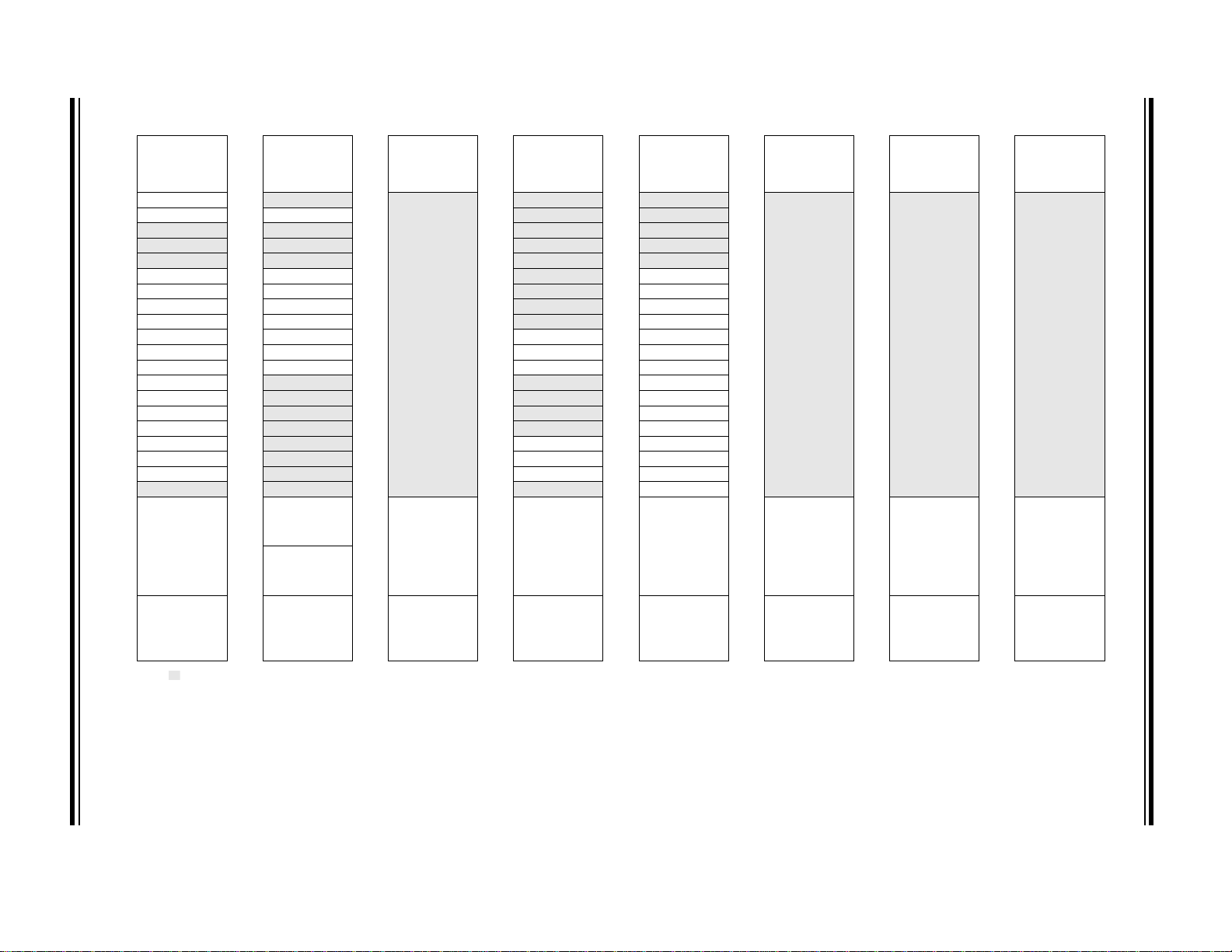
TABLE 3-3: PIC16(L)F1526/27 MEMORY MAP
BANK 0 BANK 1 BANK 2 BANK 3 BANK 4 BANK 5 BANK 6 BANK 7
000h
Core Registers
(Ta bl e 3 - 2)
00Bh 08Bh 10Bh 18Bh 20Bh 28Bh 30Bh 38Bh
00Ch PORTA 08Ch TRISA 10Ch LATA 18Ch ANSELA 20Ch
00Dh PORTB 08Dh TRISB 10Dh LATB 18Dh ANSELB 20Dh WPUB 28Dh PORTG 30Dh TRISG 38Dh LATG
00Eh PORTC 08Eh TRISC 10Eh LATC 18Eh
00Fh PORTD 08Fh TRISD 10Fh LATD 18Fh ANSELD 20Fh WPUD 28Fh
010h PORTE 090h TRISE 110h LATE 190h ANSELE 210h WPUE 290h
011h PIR1 091h PIE1 111h
012h PIR2 092h PIE2 112h
013h PIR3 093h PIE3 113h
014h PIR4 094h PIE4 114h
015h TMR0 095h OPTION_REG 115h
016h TMR1L 096h PCON 116h BORCON 196h PMCON2 216h SSP1CON2 296h
017h TMR1H 097h WDTCON 117h FVRCON 197h
018h T1CON 098h
019h T1GCON 099h OSCCON 119h
01Ah TMR2 09Ah OSCSTAT 11Ah
01Bh PR2 09Bh ADRESL 11Bh
01Ch T2CON 09Ch ADRESH 11Ch
01Dh
01Eh
01Fh
020h
06Fh 0EFh 16Fh 1EFh 26Fh 2EFh
070h
07Fh 0FFh 17Fh 1FFh 27Fh 2FFh 37Fh 3FFh
Legend: = Unimplemented data memory locations, read as ‘0’.
Note 1: PIC16F1526/27 only.
— 09Dh ADCON0 11Dh APFCON 19Dh RC1STA 21Dh SSP2CON1 29Dh CCPTMRS0 31Dh CCPR5H 39Dh —
— 09Eh ADCON1 11Eh — 19Eh TX1STA 21Eh SSP2CON2 29Eh CCPTMRS1 31Eh CCP5CON 39Eh —
—09Fh—11Fh— 19Fh BAUD1CON 21Fh SSP2CON3 29Fh CCPTMRS2 31Fh —39Fh—
General
Purpose
Register
80 Bytes
Common RAM
080h
0A0h
0F0h
Core Registers
(Ta bl e 3 - 2)
—118h—198h—218h— 298h CCPR2L 318h CCPR4L 398h —
General
Purpose
Register
80 Bytes
Common RAM
(Accesses
70h – 7Fh)
100h
120h
170h
Core Registers
(Table 3-2)
— 191h PMADRL 211h SSP1BUF 291h CCPR1L 311h CCPR3L 391h —
— 192h PMADRH 212h SSP1ADD 292h CCPR1H 312h CCPR3H 392h —
— 193h PMDATL 213h SSP1MSK 293h CCP1CON 313h CCP3CON 393h —
— 194h PMDATH 214h SSP1STAT 294h — 314h — 394h IOCBP
— 195h PMCON1 215h SSP1CON1 295h — 315h — 395h IOCBN
— 199h RC1REG 219h SSP2BUF 299h CCPR2H 319h CCPR4H 399h —
— 19Ah TX1REG 21Ah SSP2ADD 29Ah CCP2CON 31Ah CCP4CON 39Ah —
— 19Bh SP1BRG 21Bh SSP2MSK 29Bh —31Bh—39Bh—
— 19Ch SP1BRGH 21Ch SSP2STAT 29Ch — 31Ch CCPR5L 39Ch —
General
Purpose
Register
80 Bytes
Common RAM
(Accesses
70h – 7Fh)
180h
1A0h
1F0h
Core Registers
(Table 3-2)
—20Eh—28Eh—30Eh—38Eh—
VREGCON
General
Purpose
Register
80 Bytes
Common RAM
(Accesses
70h – 7Fh)
200h
Core Registers
(Table 3-2)
— 28Ch PORTF 30Ch TRISF 38Ch LATF
(1)
217h SSP1CON3 297h — 317h — 397h —
220h
General
Purpose
Register
80 Bytes
270h
Common RAM
(Accesses
70h – 7Fh)
280h
2A0h
2F0h
Core Registers
(Table 3-2)
—30Fh—38Fh—
— 310h — 390h —
— 316h — 396h IOCBF
General
Purpose
Register
80 Bytes
Common RAM
(Accesses
70h – 7Fh)
300h
Core Registers
(Table 3-2)
320h
General
Purpose
Register
80 Bytes
36Fh 3EFh
370h
Common RAM
(Accesses
70h – 7Fh)
380h
3A0h
3F0h
Core Registers
(Table 3-2)
General
Purpose
Register
80 Bytes
Common RAM
(Accesses
70h – 7Fh)
PIC16(L)F1526/27
DS41458A-page 26 Preliminary 2011 Microchip Technology Inc.
Legend: = Unimplemented data memory locations, read as ‘0’.
Note 1: PIC16(L)F1527 only.
BANK 8 BANK 9 BANK 10 BANK 11 BANK 12 BANK 13 BANK 14 BANK 15
400h
40Bh
Core Registers
(Ta bl e 3 -2 )
480h
48Bh
Core Registers
(Ta bl e 3 -2 )
500h
50Bh
Core Registers
(Ta bl e 3 -2 )
580h
58Bh
Core Registers
(Ta bl e 3 -2 )
600h
60Bh
Core Registers
(Ta bl e 3 -2 )
680h
68Bh
Core Registers
(Ta bl e 3 -2 )
700h
70Bh
Core Registers
(Ta bl e 3 -2 )
780h
78Bh
Core Registers
(Ta bl e 3 -2 )
40Ch
ANSELF
48Ch
—
50Ch
Unimplemented
Read as ‘0’
58Ch
—
60Ch
—
68Ch
Unimplemented
Read as ‘0’
70Ch
Unimplemented
Read as ‘0’
78Ch
Unimplemented
Read as ‘0’
40Dh
ANSELG
48Dh
WPUG
58Dh
—
60Dh
—
40Eh
—
48Eh
—
58Eh
—
60Eh
—
40Fh
—
48Fh
—
58Fh
—
60Fh
—
410h
—
490h
—
590h
—
610h
—
411h
TMR3L
491h
RC2REG
591h
—
611h
CCPR6L
412h
TMR3H
492h
TX2REG
592h
—
612h
CCPR6H
413h
T3CON
493h
SP2BRG
593h
—
613h
CCP6CON
414h
T3GCON
494h
SP2BRGH
594h
—
614h
CCPR7L
415h
TMR4
495h
RC2STA
595h
TMR8
615h
CCPR7H
416h
PR4
496h
TX2STA
596h
PR8
616h
CCP7CON
417h
T4CON
497h
BAUD2CON
597h
T8CON
617h
CCPR8L
418h
TMR5L
498h
—
598h
—
618h
CCPR8H
419h
TMR5H
499h
—
599h
—
619h
CCP8CON
41Ah
T5CON
49Ah
—
59Ah
—
61Ah
CCPR9L
41Bh
T5GCON
49Bh
—
59Bh
—
61Bh
CCPR9H
41Ch
TMR6
49Ch
—
59Ch
TMR10
61Ch
CCP9CON
41Dh
PR6
49Dh
—
59Dh
PR10
61Dh
CCPR10L
41Eh
T6CON
49Eh
—
59Eh
T10CON
61Eh
CCPR10H
41Fh
—
49Fh
—
51Fh 59Fh
—
61Fh
CCP10CON
69Fh 71Fh 79Fh
420h
General
Purpose
Register
80 Bytes
4A0h
General Purpose
Register
32 Bytes
520h
General
Purpose
Register
80 Bytes
(1)
5A0h
General
Purpose
Register
80 Bytes
(1)
620h
General
Purpose
Register
80 Bytes
(1)
6A0h
General
Purpose
Register
80 Bytes
(1)
720h
General
Purpose
Register
80 Bytes
(1)
7A0h
General
Purpose
Register
80 Bytes
(1)
4BFh
4C0h
General Purpose
Register
48 Bytes
(1)
46Fh 4EFh 56Fh 5EFh 66Fh 6EFh 76Fh 7EFh
470h
Common RAM
(Accesses
70h – 7Fh)
4F0h
Common RAM
(Accesses
70h – 7Fh)
570h
Common RAM
(Accesses
70h – 7Fh)
5F0h
Common RAM
(Accesses
70h – 7Fh)
670h
Common RAM
(Accesses
70h – 7Fh)
6F0h
Common RAM
(Accesses
70h – 7Fh)
770h
Common RAM
(Accesses
70h – 7Fh)
7F0h
Common RAM
(Accesses
70h – 7Fh)
47Fh
4FFh 57Fh
5FFh 67Fh 6FFh 77Fh 7FFh
TABLE 3-3: PIC16(L)F1526/27 MEMORY MAP (CONTINUED)
PIC16(L)F1526/27

2011 Microchip Technology Inc. Preliminary DS41458A-page 27
TABLE 3-3: PIC16(L)F1526/27 MEMORY MAP (CONTINUED)
BANK 16 BANK 17 BANK 18 BANK 19 BANK 20 BANK 21 BANK 22 BANK 23
800h
Core Registers
(Ta bl e 3 - 2)
80Bh
80Ch
Unimplemented
Read as ‘0’
81Fh 89Fh 91Fh
820h
86Fh 8EFh 96Fh
870h
87Fh 8FFh 97Fh 9FFh A7Fh AFFh B7Fh BFFh
General
Purpose
Register
80 Bytes
Common RAM
(Accesses
70h – 7Fh)
BANK 24 BANK 25 BANK 26 BANK 27 BANK 28 BANK 29 BANK 30
C00h
Core Registers
(Ta bl e 3 - 2)
C0Bh
C0Ch
Unimplemented
Read as ‘0’
C6Fh
C70h
Common RAM
(Accesses
C7Fh
70h – 7Fh)
880h
Core Registers
(Ta bl e 3 - 2)
88Bh
88Ch
Unimplemented
Read as ‘0’
8A0h
(1)
8F0h
C80h
C8Bh
C8Ch
CEFh
CF0h
CFFh D7Fh DFFh E7Fh EFFh F7Fh
General
Purpose
Register
80 Bytes
Common RAM
(Accesses
70h – 7Fh)
Core Registers
(Ta bl e 3 - 2)
Unimplemented
Read as ‘0’
Common RAM
(Accesses
70h – 7Fh)
900h
Core Registers
(Table 3-2)
90Bh
90Ch
Unimplemented
Read as ‘0’
920h
(1)
970h
D00h
D0Bh
D0Ch
D6Fh
D70h
General
Purpose
Register
80 Bytes
Common RAM
(Accesses
70h – 7Fh)
Core Registers
(Table 3-2)
Unimplemented
Read as ‘0’
Common RAM
(Accesses
70h – 7Fh)
980h
Core Registers
(Table 3-2)
98Bh
98Ch
Unimplemented
Read as ‘0’
(1)
9EFh
9F0h
Common RAM
(Accesses
70h – 7Fh)
D80h
Core Registers
(Table 3-2)
D8Bh
D8Ch
Unimplemented
Read as ‘0’
DEFh
DF0h
Common RAM
(Accesses
70h – 7Fh)
A00h
A0Bh
A0Ch
A6Fh
A70h
E00h
E0Bh
E0Ch
E6Fh
E70h
Core Registers
(Table 3-2)
Unimplemented
Read as ‘0’
Common RAM
(Accesses
70h – 7Fh)
Core Registers
(Table 3-2)
Unimplemented
Read as ‘0’
Common RAM
(Accesses
70h – 7Fh)
A80h
A8Bh
A8Ch
AEFh
AF0h
E80h
E8Bh
E8Ch
EEFh
EF0h
Core Registers
(Table 3-2)
Unimplemented
Read as ‘0’
Common RAM
(Accesses
70h – 7Fh)
Core Registers
(Table 3-2)
Unimplemented
Read as ‘0’
Common RAM
(Accesses
70h – 7Fh)
B00h
B0Bh
B0Ch
B6Fh
B70h
F00h
F0Bh
F0Ch
F6Fh
F70h
Core Registers
(Table 3-2)
Unimplemented
Read as ‘0’
Common RAM
(Accesses
70h – 7Fh)
Core Registers
(Table 3-2)
Unimplemented
Read as ‘0’
Common RAM
(Accesses
70h – 7Fh)
B80h
B8Bh
B8Ch
BEFh
BF0h
Core Registers
(Table 3-2)
Unimplemented
Read as ‘0’
Common RAM
(Accesses
70h – 7Fh)
PIC16(L)F1526/27
Legend: = Unimplemented data memory locations, read as ‘0’.
Note 1: PIC16(L)F1527 only.
DS41458A-page 28 Preliminary 2011 Microchip Technology Inc.
Legend: = Unimplemented data memory locations, read as ‘0’.
Bank 31
F80h
F8Bh
Core Registers
(Ta bl e 3 -2 )
F8Ch
FE3h
Unimplemented
Read as ‘0’
FE4h
STATUS_SHAD
FE5h
WREG_SHAD
FE6h
BSR_SHAD
FE7h
PCLATH_SHAD
FE8h
FSR0L_SHAD
FE9h
FSR0H_SHAD
FEAh
FSR1L_SHAD
FEBh
FSR1H_SHAD
FECh
—
FEDh
STKPTR
FEEh
TOSL
FEFh
TOSH
FF0h
Common RAM
(Accesses
70h – 7Fh)
FFFh
TABLE 3-3: PIC16(L)F1526 MEMORY MAP (CONTINUED)
PIC16(L)F1526/27

PIC16(L)F1526/27
3.2.6 CORE FUNCTION REGISTERS SUMMARY
The Core Function registers listed in Ta bl e 3 - 4 can be
addressed from any Bank.
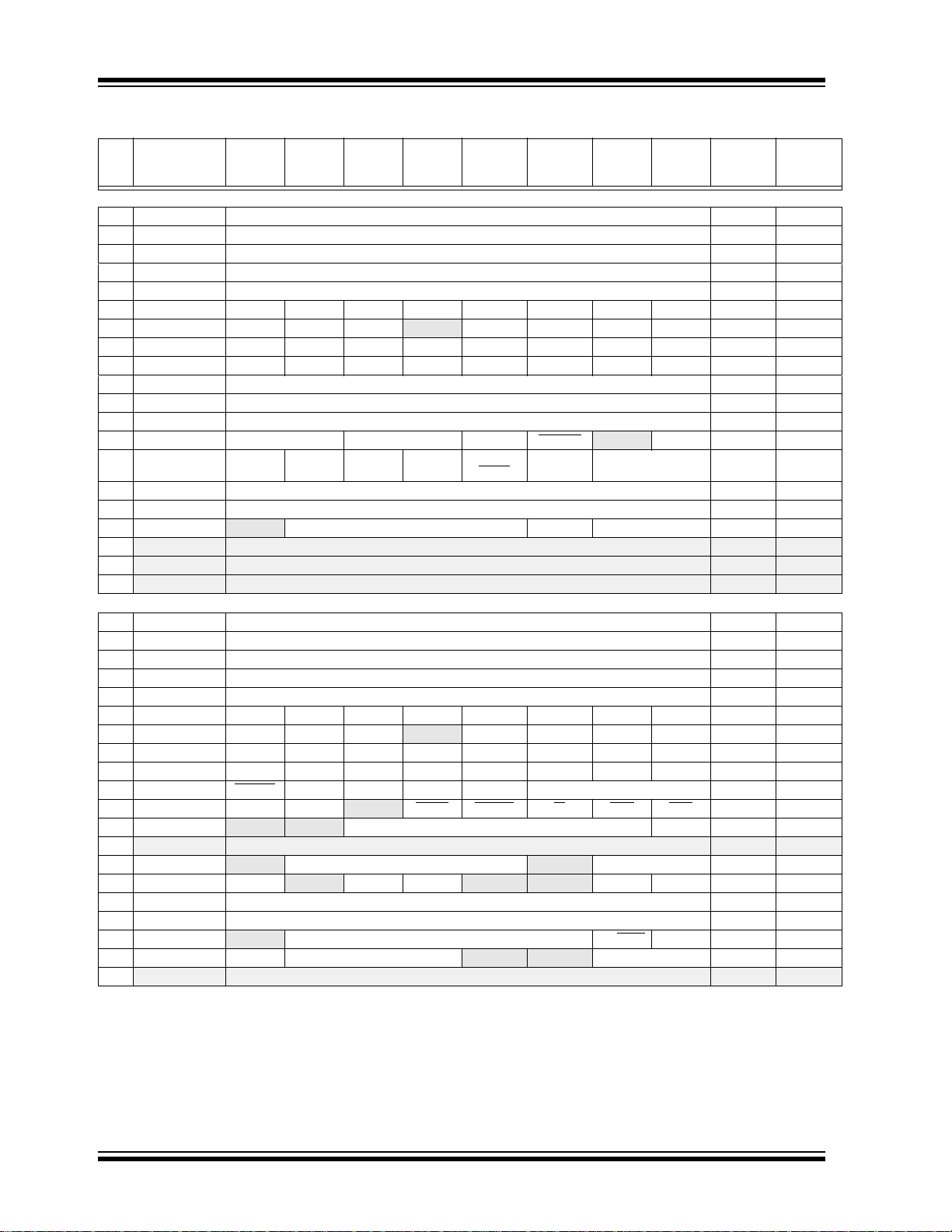
TABLE 3-4: CORE FUNCTION REGISTERS SUMMARY
Addr Name Bit 7 Bit 6 Bit 5 Bit 4 Bit 3 Bit 2 Bit 1 Bit 0
Bank 0-31
x00h or
INDF0
x80h
x01h or
INDF1
x81h
x02h or
PCL Program Counter (PC) Least Significant Byte 0000 0000 0000 0000
x82h
x03h or
STATUS
x83h
x04h or
FSR0L Indirect Data Memory Address 0 Low Pointer 0000 0000 uuuu uuuu
x84h
x05h or
FSR0H Indirect Data Memory Address 0 High Pointer 0000 0000 0000 0000
x85h
x06h or
FSR1L Indirect Data Memory Address 1 Low Pointer 0000 0000 uuuu uuuu
x86h
x07h or
FSR1H Indirect Data Memory Address 1 High Pointer 0000 0000 0000 0000
x87h
x08h or
BSR
x88h
x09h or
WREG Working Register 0000 0000 uuuu uuuu
x89h
x0Ah or
PCLATH
x8Ah
x0Bh or
INTCON GIE PEIE TMR0IE INTE IOCIE TMR0IF INTF IOCIF 0000 0000 0000 0000
x8Bh
Legend: x = unknown, u = unchanged, q = value depends on condition, - = unimplemented, read as ‘0’, r = reserved.
Addressing this location uses contents of FSR0H/FSR0L to address data memory
(not a physical register)
Addressing this location uses contents of FSR1H/FSR1L to address data memory
(not a physical register)
— — —TOPD ZDCC---1 1000 ---q quuu
— — — BSR4 BSR3 BSR2 BSR1 BSR0 ---0 0000 ---0 0000
— Write Buffer for the upper 7 bits of the Program Counter -000 0000 -000 0000
Shaded locations are unimplemented, read as ‘0’.
Value on
POR, BOR
xxxx xxxx uuuu uuuu
xxxx xxxx uuuu uuuu
Value on all
other Resets
2011 Microchip Technology Inc. Preliminary DS41458A-page 29
PIC16(L)F1526/27
TABLE 3-2: SPECIAL FUNCTION REGISTER SUMMARY
Addr Name Bit 7 Bit 6 Bit 5 Bit 4 Bit 3 Bit 2 Bit 1 Bit 0
Value on
POR, BOR
Bank 0
00Ch PORTA PORTA Data Latch when written: PORTA pins when read xxxx xxxx uuuu uuuu
00Dh PORTB PORTB Data Latch when written: PORTB pins when read xxxx xxxx uuuu uuuu
00Eh PORTC PORTC Data Latch when written: PORTC pins when read xxxx xxxx uuuu uuuu
00Fh PORTD PORTD Data Latch when written: PORTD pins when read xxxx xxxx uuuu uuuu
010h PORTE PORTE Data Latch when written: PORTE pins when read xxxx xxxx uuuu uuuu
011h PIR1 TMR1GIF ADIF RC1IF TX1IF SSP1IF CCP1IF TMR2IF TMR1IF 0000 0000 0000 0000
012h PIR2 OSFIF TMR5GIF TMR3GIF
013h PIR3 CCP6IF CCP5IF CCP4IF CCP3IF TMR6IF TMR5IF TMR4IF TMR3IF 0000 0000 0000 0000
014h PIR4 CCP10IF CCP9IF RC2IF TX2IF CCP8IF CCP7IF BCL2IF SSP2IF 0000 0000 0000 0000
015h TMR0 Timer0 Module Register xxxx xxxx uuuu uuuu
016h TMR1L Holding Register for the Least Significant Byte of the 16-bit TMR1 Register xxxx xxxx uuuu uuuu
017h TMR1H Holding Register for the Most Significant Byte of the 16-bit TMR1 Register xxxx xxxx uuuu uuuu
018h T1CON TMR1CS<1:0> T1CKPS<1:0> SOSCEN T1SYNC
019h T1GCON TMR1GE T1GPOL T1GTM T1GSPM T1GGO/
01Ah TMR2 Timer 2 Module Register 0000 0000 0000 0000
01Bh PR2 Timer 2 Period Register 1111 1111 1111 1111
01Ch T2CON
01Dh
— Unimplemented — —
01Eh
— Unimplemented — —
01Fh
— Unimplemented — —
— T2OUTPS<3:0> TMR2ON T2CKPS<1:0> -000 0000 -000 0000
— BCL1IF TMR10IF TMR8IF CCP2IF 000- 0000 000- 0000
—TMR1ON0000 00-0 uuuu uu-u
DONE
T1GVAL T1GSS<1:0> 0000 0x00 uuuu uxuu
Bank 1
08Ch TRISA PORTA Data Direction Register 1111 1111 1111 1111
08Dh TRISB PORTB Data Direction Register 1111 1111 1111 1111
08Eh TRISC PORTC Data Direction Register 1111 1111 1111 1111
08Fh TRISD PORTD Data Direction Register 1111 1111 1111 1111
090h TRISE PORTE Data Direction Register 1111 1111 1111 1111
091h PIE1 TMR1GIE ADIE RC1IE TX1IE SSP1IE CCP1IE TMR2IE TMR1IE 0000 0000 0000 0000
092h PIE2 OSFIE TMR5GIE TMR3GIE
093h PIE3 CCP6IE CCP5IE CCP4IE CCP3IE TMR6IE TMR5IE TMR4IE TMR3IE 0000 0000 0000 0000
094h PIE4 CCP10IE CCP9IE
095h
OPTION_REG
096h PCON STKOVF STKUNF
097h WDTCON
098h
— Unimplemented — —
099h OSCCON
09Ah OSCSTAT SOSCR
09Bh ADRESL A/D Result Register Low xxxx xxxx uuuu uuuu
09Ch ADRESH A/D Result Register High xxxx xxxx uuuu uuuu
09Dh ADCON0
09Eh ADCON1 ADFM ADCS<2:0>
09Fh
— Unimplemented — —
Legend: x = unknown, u = unchanged, q = value depends on condition, - = unimplemented, read as ‘0’, r = reserved.
Note 1: PIC16F1526/7 only.
Shaded locations are unimplemented, read as ‘0’.
2: Unimplemented, read as ‘1’.
WPUEN INTEDG TMR0CS TMR0SE PSA PS<2:0> 1111 1111 1111 1111
— —WDTPS<4:0>SWDTEN--01 0110 --01 0110
— IRCF<3:0> —SCS<1:0>-011 1-00 -011 1-00
— OSTS HFIOFR — — LFIOFR HFIOFS 0-q0 --00 q-qq --0q
— CHS<4:0>
RC2IE TX2IE CCP8IE CCP7IE BCL2IE SSP2IE 0000 0000 0000 0000
—RWDTRMCLR RI POR BOR 00-1 11qq qq-q qquu
— BCL1IE TMR10IE TMR8IE CCP2IE 000- 0000 000- 0000
GO/DONE
— —
ADON -000 0000 -000 0000
ADPREF<1:0>
0000 --00 0000 --00
Value on all
other
Resets
DS41458A-page 30 Preliminary 2011 Microchip Technology Inc.
 Loading...