


PIC16(L)F1507
Data Sheet
20-Pin Flash, 8-Bit Microcontrollers
2011 Microchip Technology Inc. Preliminary DS41586A
Note the following details of the code protection feature on Microchip devices:
• Microchip products meet the specification contained in their particular Microchip Data Sheet.
• Microchip believes that its family of products is one of the most secure families of its kind on the market today, when used in the
intended manner and under normal conditions.
• There are dishonest and possibly illegal methods used to breach the code protection feature. All of these methods, to our
knowledge, require using the Microchip products in a manner outside the operating specifications contained in Microchip’s Data
Sheets. Most likely, the person doing so is engaged in theft of intellectual property.
• Microchip is willing to work with the customer who is concerned about the integrity of their code.
• Neither Microchip nor any other semiconductor manufacturer can guarantee the security of their code. Code protection does not
mean that we are guaranteeing the product as “unbreakable.”
Code protection is constantly evolving. We at Microchip are committed to continuously improving the code protection features of our
products. Attempts to break Microchip’s code protection feature may be a violation of the Digital Millennium Copyright Act. If such acts
allow unauthorized access to your software or other copyrighted work, you may have a right to sue for relief under that Act.
Information contained in this publication regarding device
applications and the like is provided only for your convenience
and may be superseded by updates. It is your responsibility to
ensure that your application meets with your specifications.
MICROCHIP MAKES NO REPRESENTATIONS OR
WARRANTIES OF ANY KIND WHETHER EXPRESS OR
IMPLIED, WRITTEN OR ORAL, STATUTORY OR
OTHERWISE, RELATED TO THE INFORMATION,
INCLUDING BUT NOT LIMITED TO ITS CONDITION,
QUALITY, PERFORMANCE, MERCHANTABILITY OR
FITNESS FOR PURPOSE. Microchip disclaims all liability
arising from this information and its use. Use of Microchip
devices in life support and/or safety applications is entirely at
the buyer’s risk, and the buyer agrees to defend, indemnify and
hold harmless Microchip from any and all damages, claims,
suits, or expenses resulting from such use. No licenses are
conveyed, implicitly or otherwise, under any Microchip
intellectual property rights.
Trademarks
The Microchip name and logo, the Microchip logo, dsPIC,
K
EELOQ, KEELOQ logo, MPLAB, PIC, PICmicro, PICSTART,
32
PIC
logo, rfPIC and UNI/O are registered trademarks of
Microchip Technology Incorporated in the U.S.A. and other
countries.
FilterLab, Hampshire, HI-TECH C, Linear Active Thermistor,
MXDEV, MXLAB, SEEVAL and The Embedded Control
Solutions Company are registered trademarks of Microchip
Technology Incorporated in the U.S.A.
Analog-for-the-Digital Age, Application Maestro, chipKIT,
chipKIT logo, CodeGuard, dsPICDEM, dsPICDEM.net,
dsPICworks, dsSPEAK, ECAN, ECONOMONITOR,
FanSense, HI-TIDE, In-Circuit Serial Programming, ICSP,
Mindi, MiWi, MPASM, MPLAB Certified logo, MPLIB,
MPLINK, mTouch, Omniscient Code Generation, PICC,
PICC-18, PICDEM, PICDEM.net, PICkit, PICtail, REAL ICE,
rfLAB, Select Mode, Total Endurance, TSHARC,
UniWinDriver, WiperLock and ZENA are trademarks of
Microchip Technology Incorporated in the U.S.A. and other
countries.
SQTP is a service mark of Microchip Technology Incorporated
in the U.S.A.
All other trademarks mentioned herein are property of their
respective companies.
© 2011, Microchip Technology Incorporated, Printed in the
U.S.A., All Rights Reserved.
Printed on recycled paper.
ISBN: 978-1-61341-342-5
Microchip received ISO/TS-16949:2002 certification for its worldwide
headquarters, design and wafer fabrication facilities in Chandler and
Tempe, Arizona; Gresham, Oregon and design centers in California
and India. The Company’s quality system processes and procedures
are for its PIC
devices, Serial EEPROMs, microperipherals, nonvolatile memory and
analog products. In addition, Microchip’s quality system for the design
and manufacture of development systems is ISO 9001:2000 certified.
®
MCUs and dsPIC® DSCs, KEELOQ
®
code hopping
DS41586A-page 2 Preliminary 2011 Microchip Technology Inc.

PIC16(L)F1507
20-Pin Flash, 8-Bit Microco ntr ollers
High-Performance RISC CPU:
• C Compiler Optimized Architecture
• Only 49 Instructions
• Up to 3.5 Kbytes Linear Program Memory
Addressing
• Up to 128 bytes Linear Data Memory Addressing
• Operating Speed:
- DC – 20 MHz clock input
- DC – 125 ns instruction cycle
• Interrupt Capability with Automatic Context
Saving
• 16-Level Deep Hardware Stack with Optional
Overflow/Underflow Reset
• Direct, Indirect and Relative Addressing modes:
- Two full 16-bit File Select Registers (FSRs)
- FSRs can read program and data memory
Flexible Oscillator Struc ture:
• 16 MHz Internal Oscillator Block:
- Factory calibrated to 1%, typical
- Software selectable frequency range from
16 MHz to 31 kHz
• 31 kHz Low-Power Internal Oscillator
• Three External Clock modes up to 20 MHz
Special Microcontroller Features:
• Operating Voltage Range:
- 1.8V to 3.6V (PIC16LF1507)
- 2.3V to 5.5V (PIC16F1507)
• Self-Programmable under Software Control
• Power-on Reset (POR)
• Power-up Timer (PWRT)
• Programmable Low-Power Brown-Out Reset
(LPBOR)
• Extended Watch-Dog Timer (WDT):
- Programmable period from 1 ms to 256s
• Programmable Code Protection
• In-Circuit Serial Programming™ (ICSP™) via two
pins
• Enhanced Low-Voltage Programming (LVP)
• Power-Saving Sleep mode
Low-Power Features (PIC16LF1507):
• Standby Current:
- 20 nA @ 1.8V, typical
• Operating Current:
-30A per MHz @ 1.8V, typical
• Low-Power Watchdog Timer Current:
- 300 nA @ 1.8V, typical
Analog Features:
• Analog-to-Digital Converter (ADC):
- 10-bit resolution
- Up to 12 channels
- Auto acquisition capability
- Conversion available during Sleep
- FVR available as channel
• Voltage Reference module:
- Fixed Voltage Reference (FVR) with 1.024V,
2.048V and 4.096V output levels
Peripheral Features:
• 17 I/O Pins and 1 Input-only Pin:
- High current sink/source 25 mA/25 mA
- Individually programmable weak pull-ups
- Individually programmable
interrupt-on-change (IOC) pins
• Timer0: 8-Bit Timer/Counter with 8-Bit
Programmable Prescaler
• Enhanced Timer1:
- 16-bit timer/counter with prescaler
- External Gate Input mode
• Timer2: 8-Bit Timer/Counter with 8-Bit Period
Register, Prescaler and Postscaler
• Four 10-bit PWM modules
• Two Configurable Logic Cell (CLC) modules:
- 22 individual input sources
- Four inputs and 16 selectable input sources
per module
- Software selectable logic functions including:
AND/OR/XOR/D Flop/D Latch/SR/JK
- External and internal inputs/outputs
- Operation while in Sleep
• Numerically Controlled Oscillator (NCO):
- 20-bit Accumulator
- 16-bit Increment
- Linear frequency control
- High-speed clock input
- Selectable Output modes
- Fixed Duty Cycle (FDC) mode
- Pulse Frequency (PF) mode
• Complementary Waveform Generator (CWG):
- 6 selectable signal sources
- Selectable falling and rising edge dead-band
control
- Polarity control
- 2 auto-shutdown sources
- Multiple input sources: PWM, CLC, NCO
2011 Microchip Technology Inc. Preliminary DS41586A-page 3

PIC16(L)F1507 Family Types
PIC16F1507
PIC16LF1507
1
2
3
4
14
13
12
11
5
6
7
10
9
8
VDD
RA5
RA4
MCLR
/VPP/RA3
RC5
RC4
V
SS
RA0/ICSPDAT
RA1/ICSPCLK
RA2
RC0
RC1
RC2
RC3
PDIP, SOIC, SSOP
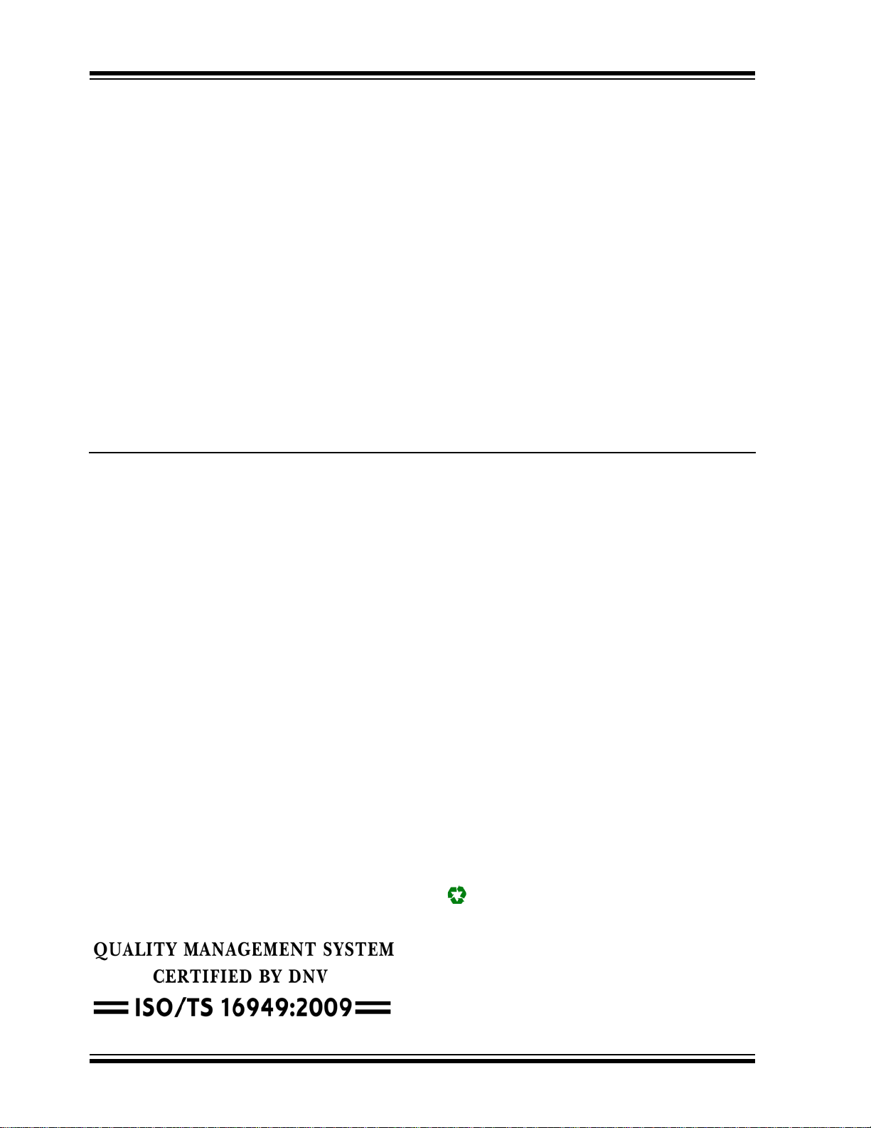
Note: See Tab le 1 for location of all peripheral functions.
18
17
16
15
20
19
RC6
RC7
RB7
RB4
RB5
RB6
PIC16(L)F1507
Program
Device
PIC16F1507
PIC16LF1507
Note1: One pin is input-only.
Memory Flash
(words)
2048 128 18 12 2/1 4 1 2 1
SRAM
(bytes)
I/O
10-bit A/D
(1)
(ch)
Timers
8/16-bit
PWM CWG CLC NCO
FIGURE 1: 20-PIN PDIP, SOIC, SSOP PACKAGE DIAGRAM FOR PIC16(L)F1507
2011 Microchip Technology Inc. Preliminary DS41586A-page 4
PIC16(L)F1507
PIC16
F1507
PIC16LF1507
QFN 4x4
Note: See Tab le 1 for location of all peripheral functions.
15
RA1/ICSPCLK
RA2
RC0
RC1
RC2
11
12
13
14
6
7
RC7
RB7
RB4
RB5
RB6
8
9
10
2
3
1
1819
20
1617
5
4
VDD
RA5
RA4
MCLR/VPP/RA3
RC5
RC4
RC3
RC6
VSS
RA0/ICSPDAT
FIGURE 2: 20-PIN QFN PACKAGE DIAGRAM FOR PIC16(L)F1507
DS41586A-page 5 Preliminary 2011 Microchip Technology Inc.

TABLE 1: 20-PIN ALLOCATION TABLE (PIC16(L)F1507)
PIC16(L)F1507
I/O
20-Pin PDIP/SOIC/SSOP
RA0 19 16 AN0 — — — — — — IOC Y ICSPDAT
RA1 18 15 AN1 VREF+ — — — — — IOC Y ICSPCLK
RA2 17 14 AN2 — CWG1FLT — CLC1
RA3 4 1 — — — — CLC1IN0 — — IOC Y MCLR
RA4 3 20 AN3 — — — — T1G — IOC Y CLKOUT
RA5 2 19 — — — NCO1CLK — T1CKI — IOC Y CLKIN
RB4 13 10 AN10 — — — — — — IOC Y —
RB5 12 9 AN11 — — — — — — IOC Y —
RB6 11 8 — — — — — — — IOC Y —
RB7 10 7 — — — — — — — IOC Y —
RC0 16 13 AN4 — — — CLC2 — — — — —
RC1 15 12 AN5 — — NCO1
RC2 14 11 AN6 — — — — — — — — —
RC3 7 4 AN7 — — — CLC2IN0 — PWM2 — — —
RC4 6 3 — — CWG1B — CLC2IN1 — — — — —
RC5 5 2 — — CWG1A — CLC1
RC6 8 5 AN8 — — NCO1
RC7 9 6 AN9 — — — CLC1IN1 — — — — —
VDD 1 18 — — — — — — — — — VDD
VSS 20 17 — — — — — — — — — VSS
Note 1: Default location for peripheral pin function. Alternate location can be selected using the APFCON register.
2: Alternate location for peripheral pin function selected by the APFCON register.
A/D
20-Pin QFN
Reference
CWG
NCO
(1)
(2)
CLC
(1)
— — PWM4 — — —
(2)
— — — — — —
Timers
T0CKI PWM3 INT/
— PWM1 — — —
PWM
IOC
Interrupt
Y —
Pull-up
VPP
Basic
2011 Microchip Technology Inc. Preliminary DS41586A-page 6

PIC16(L)F1507
Table of Contents
1.0 Device Overview ............................................................................................................................................................................. 9
2.0.Enhanced Mid-Range CPU ........................................................................................................................................................... 13
3.0 Memory Organization.................................................................................................................................................................... 15
4.0 Device Configuration..................................................................................................................................................................... 39
5.0 Oscillator Module (With Fail-Safe Clock Monitor) ......................................................................................................................... 45
6.0 Resets........................................................................................................................................................................................... 53
7.0 Interrupts ....................................................................................................................................................................................... 61
8.0 Power-Down Mode (Sleep) ........................................................................................................................................................... 75
9.0 Watchdog Timer............................................................................................................................................................................ 79
10.0 Flash Program Memory Control .................................................................................................................................................. 83
11.0 I/O Ports ...................................................................................................................................................................................... 99
12.0 Interrupt-On-Change ................................................................................................................................................................. 111
13.0 Fixed Voltage Reference (FVR) ................................................................................................................................................ 117
14.0 Temperature Indicator Module .................................................................................................................................................. 119
15.0 Analog-to-Digital Converter (ADC) Module ............................................................................................................................... 121
16.0 Timer0 Module .......................................................................................................................................................................... 135
17.0 Timer1 Module with Gate Control ............................................................................................................................................. 139
18.0 Timer2 Modules ........................................................................................................................................................................ 151
19.0 PWM Modules ........................................................................................................................................................................... 155
20.0 Configurable Logic Cell (CLC) ................................................................................................................................................... 161
21.0 Numerically Controlled Oscillator (NCO) Module ...................................................................................................................... 177
22.0 Complementary Waveform Generator (CWG) Module ............................................................................................................. 187
23.0 In-Circuit Serial Programming™ (ICSP™)................................................................................................................................ 203
24.0 Instruction Set Summary ........................................................................................................................................................... 207
25.0 Electrical Specifications ............................................................................................................................................................ 221
26.0 DC and AC Characteristics Graphs and Charts ........................................................................................................................ 239
27.0 Development Support ............................................................................................................................................................... 241
28.0 Packaging Information .............................................................................................................................................................. 245
Appendix A: Data Sheet Revision History ......................................................................................................................................... 255
Index ................................................................................................................................................................................................. 257
The Microchip Web Site .................................................................................................................................................................... 263
Customer Change Notification Service ............................................................................................................................................. 263
Customer Support ............................................................................................................................................................................. 263
Reader Response ............................................................................................................................................................................. 264
Product Identification System ............................................................................................................................................................ 265
Worldwide Sales and Service ........................................................................................................................................................... 266
DS41586A-page 7 Preliminary 2011 Microchip Technology Inc.

NOTES:
PIC16(L)F1507
2011 Microchip Technology Inc. Preliminary DS41586A-page 8

PIC16(L)F1507
1.0 DEVICE OVERVIEW
The PIC16(L)F1507 are described within this data sheet.
They are available in 20 pin packages. Figure 1-1 shows
a block diagram of the PIC16(L)F1507 devices.
Tables 1-2 shows the pinout descriptions.
Reference Ta bl e 1 - 1 for peripherals available per
device.
TABLE 1-1: DEVICE PERIPHERAL
SUMMARY
Peripheral
PIC16F1507
PIC16LF1507
Analog-to-Digital Converter (ADC) ●●
Complementary Wave Generator (CWG) ●●
Fixed Voltage Reference (FVR) ●●
Numerically Controlled Oscillator (NCO) ●●
Temperature Indicator ●●
Configurable Logic Cell (CLC)
CLC1 ●●
CLC2 ●●
PWM Modules
PWM1 ●●
PWM2 ●●
PWM3 ●●
PWM4 ●●
Timers
Timer0 ●●
Timer1 ●●
Timer2 ●●
DS41586A-page 9 Preliminary 2011 Microchip Technology Inc.
FIGURE 1-1: PIC16(L)F1507 BLOCK DIAGRAM
PORTB
PORTC
Note 1: See applicable chapters for more information on peripherals.
2: See Ta bl e 1 -1 for peripherals available on specific devices.
CPU
Program
Flash Memory
RAM
Timing
Generation
INTRC
Oscillator
MCLR
(Figure 2-1)
NCO1
PWM4
Timer2Timer1Timer0
CLC2
PWM1 PWM2
PWM3
PORTA
CWG1
CLC1
ADC
10-Bit
FVR
Te mp .
Indicator
CLKIN
CLKOUT
PIC16(L)F1507
2011 Microchip Technology Inc. Preliminary DS41586A-page 10
PIC16(L)F1507
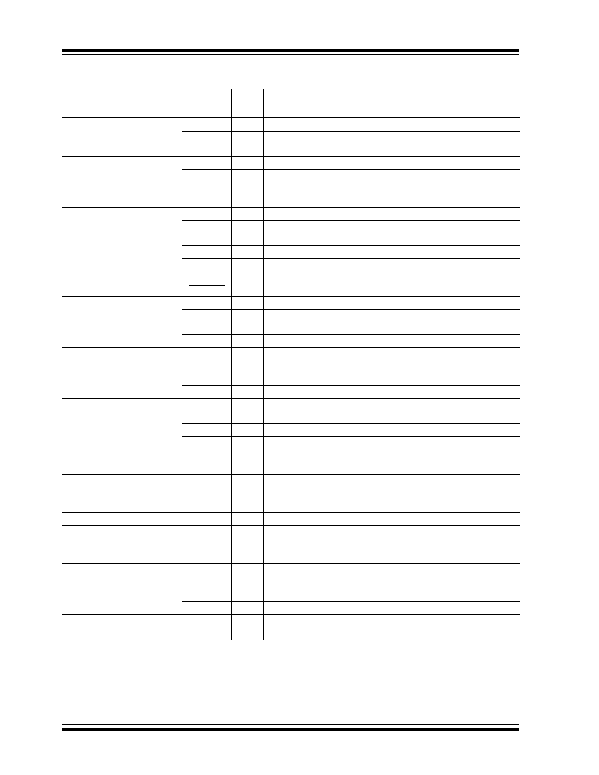
TABLE 1-2: PIC16(L)F1507 PINOUT DESCRIPTION
Input
Name Function
RA0/AN0/ICSPDAT RA0 TTL CMOS General purpose I/O.
AN0 AN — A/D Channel input.
ICSPDAT ST CMOS ICSP™ Data I/O.
RA1/AN1/V
RA2/AN2/T0CKI/INT/PWM3/
CLC1
RA3/CLC1IN0/V
RA4/AN3/CLKOUT/T1G RA4 TTL CMOS General purpose I/O.
RA5/CLKIN/T1CKI/NCO1CLK RA5 TTL CMOS General purpose I/O.
RB4/AN10 RB4 TTL CMOS General purpose I/O.
RB5/AN11 RB5 TTL CMOS General purpose I/O.
RB6 RB6 TTL CMOS General purpose I/O.
RB7 RB7 TTL CMOS General purpose I/O.
RC0/AN4/CLC2 RC0 TTL CMOS General purpose I/O.
RC1/AN5/PWM4/NCO1
RC2/AN6 RC2 TTL CMOS General purpose I/O.
Legend: AN = Analog input or output CMOS = CMOS compatible input or output OD = Open Drain
Note 1: Default location for peripheral pin function. Alternate location can be selected using the APFCON register.
REF+/ICSPCLK RA1 TTL CMOS General purpose I/O.
AN1 AN — A/D Channel input.
REF+ AN — A/D Positive Voltage Reference input.
V
ICSPCLK ST — Serial Programming Clock.
(1)
/CWG1FLT
PP/MCLR RA3 TTL — General purpose input.
(1)
TTL = TTL compatible input ST = Schmitt Trigger input with CMOS levels I
HV = High Voltage XTAL = Crystal levels
2: Alternate location for peripheral pin function selected by the APFCON register.
RA2 ST CMOS General purpose I/O.
AN2 AN — A/D Channel input.
T0CKI ST — Timer0 clock input.
INT ST — External interrupt.
PWM3 — CMOS Pulse Width Module source output.
CLC1 — CMOS Configurable Logic Cell source output.
CWG1FLT
CLC1IN0 ST — Configurable Logic Cell source input.
PP HV — Programming voltage.
V
MCLR
AN3 AN — A/D Channel input.
CLKOUT — CMOS F
T1G ST — Timer1 Gate input.
CLKIN CMOS — External clock input (EC mode).
T1CKI ST — Timer1 clock input.
NCO1CLK ST — Numerically Controlled Oscillator Clock source input.
AN10 AN — A/D Channel input.
AN11 AN — A/D Channel input.
AN4 AN — A/D Channel input.
CLC2 — CMOS Configurable Logic Cell source output.
RC1 TTL CMOS General purpose I/O.
AN5 AN — A/D Channel input.
PWM4 — CMOS Pulse Width Module source output.
NCO1 — CMOS Numerically Controlled Oscillator is source output.
AN6 AN — A/D Channel input.
Output
Type
Type
ST — Complementary Waveform Generator Fault input.
ST — Master Clear with internal pull-up.
OSC/4 output.
Description
2
C™ = Schmitt Trigger input with I2C
DS41586A-page 11 Preliminary 2011 Microchip Technology Inc.
PIC16(L)F1507
TABLE 1-2: PIC16(L)F1507 PINOUT DESCRIPTION (CONTINUED)
Input
Name Function
RC3/AN7/PWM2/CLC2IN0 RC3 TTL CMOS General purpose I/O.
AN7 AN — A/D Channel input.
PWM2 — CMOS Pulse Width Module source output.
CLC2IN0 ST — Configurable Logic Cell source input.
RC4/CLC2IN1/CWG1B RC4 TTL CMOS General purpose I/O.
CLC2IN1 ST — Configurable Logic Cell source input.
(2)
RC5/PWM1/CLC1
CWG1A
RC6/AN8/NCO1
RC7/AN9/CLC1IN1 RC7 TTL CMOS General purpose I/O.
DD VDD Power — Positive supply.
V
SS VSS Power — Ground reference.
V
Legend: AN = Analog input or output CMOS = CMOS compatible input or output OD = Open Drain
Note 1: Default location for peripheral pin function. Alternate location can be selected using the APFCON register.
TTL = TTL compatible input ST = Schmitt Trigger input with CMOS levels I
HV = High Voltage XTAL = Crystal levels
2: Alternate location for peripheral pin function selected by the APFCON register.
/
(2)
CWG1B — CMOS CWG complementary output.
RC5 TTL CMOS General purpose I/O.
PWM1 — CMOS PWM output.
CLC1 — CMOS Configurable Logic Cell source output.
CWG1A — CMOS CWG primary output.
RC6 TTL CMOS General purpose I/O.
AN8 AN — A/D Channel input.
NCO1 — CMOS Numerically Controlled Oscillator source output.
AN8 AN — A/D Channel input.
CLC1IN1 ST — Configurable Logic Cell source input.
Type
Output
Type
Description
2
C™ = Schmitt Trigger input with I2C
2011 Microchip Technology Inc. Preliminary DS41586A-page 12

PIC16(L)F1507
2.0 ENHANCED MID-RANGE CPU
This family of devices contain an enhanced mid-range
8-bit CPU core. The CPU has 49 instructions. Interrupt
capability includes automatic context saving. The
hardware stack is 16 levels deep and has Overflow and
Underflow Reset capability. Direct, Indirect, and
Relative addressing modes are available. Two File
Select Registers (FSRs) provide the ability to read
program and data memory.
• Automatic Interrupt Context Saving
• 16-level Stack with Overflow and Underflow
• File Select Registers
• Instruction Set
2.1 Automatic Interrupt Context Saving
During interrupts, certain registers are automatically
saved in shadow registers and restored when returning
from the interrupt. This saves stack space and user
code. See Section 7.5 “Automatic Context Saving”,
for more information.
2.2 16-level St ack with Overflow and Underflow
These devices have an external stack memory 15 bits
wide and 16 words deep. A Stack Overflow or Underflow will set the appropriate bit (STKOVF or STKUNF)
in the PCON register, and if enabled will cause a software Reset. See section Section 3.4 “St ack” for more
details.
2.3 File Select Registers
There are two 16-bit File Select Registers (FSR). FSRs
can access all file registers and program memory,
which allows one Data Pointer for all memory. When an
FSR points to program memory, there is one additional
instruction cycle in instructions using INDF to allow the
data to be fetched. General purpose memory can now
also be addressed linearly, providing the ability to
access contiguous data larger than 80 bytes. There are
also new instructions to support the FSRs. See
Section 3.5 “Indirect Addressing” for more details.
2.4 Instruction Set
There are 49 instructions for the enhanced mid-range
CPU to support the features of the CPU. See
Section 24.0 “Instruction Set Summary” for more
details.
DS41586A-page 13 Preliminary 2011 Microchip Technology Inc.
FIGURE 2-1: CORE BLOCK DIAGRAM
Data Bus
8
14
Program
Bus
Instruction reg
Program Counter
8 Level Stack
(13-bit)
Direct Addr
7
12
Addr MUX
FSR reg
STATUS reg
MUX
ALU
Instruction
Decode &
Control
Timing
Generation
CLKIN
CLKOUT
8
8
12
3
Internal
Oscillator
Block
Configuration
Data Bus
8
14
Program
Bus
Instruction reg
Program Counter
8 Level Stack
(13-bit)
Direct Addr
7
Addr MUX
FSR reg
STATUS reg
MUX
ALU
W Reg
Instruction
Decode &
Control
Timing
Generation
8
8
3
Internal
Oscillator
Block
Configuration
15
Data Bus
8
14
Program
Bus
Instruction Reg
Program Counter
16-Level Stack
(15-bit)
Direct Addr
7
RAM Addr
Addr MUX
Indirect
Addr
FSR0 Reg
STATUS Reg
MUX
ALU
Instruction
Decode and
Control
Timing
Generation
8
8
3
Internal
Oscillator
Block
Configuration
Flash
Program
Memory
RAM
FSR regFSR reg
FSR1 Reg
15
15
MUX
15
Program Memory
Read (PMR)
12
FSR regFSR reg
BSR Reg
5
Power-up
Timer
Power-on
Reset
Watchdog
Timer
V
DD
Brown-out
Reset
VSSVDD VSSVDD VSS
PIC16(L)F1507
2011 Microchip Technology Inc. Preliminary DS41586A-page 14

PIC16(L)F1507
3.0 MEMORY ORGANIZATION
These devices contain the following types of memory:
• Program Memory
- Configuration Words
-Device ID
-User ID
- Flash Program Memory
• Data Memory
- Core Registers
- Special Function Registers
- General Purpose RAM
- Common RAM
TABLE 3-1: DEVICE SIZES AND ADDRESSES
Device Program Memory Space (Words) Last Program Memory Address
PIC16F1507
PIC16LF1507
2,048 07FFh
The following features are associated with access and
control of program memory and data memory:
• PCL and PCLATH
•Stack
• Indirect Addressing
3.1 Program Memory Organization
The enhanced mid-range core has a 15-bit program
counter capable of addressing 32K x 14 program
memory space. Table 3-1 shows the memory sizes
implemented. Accessing a location above these
boundaries will cause a wrap-around within the
implemented memory space. The Reset vector is at
0000h and the interrupt vector is at 0004h (See
Figure 3-1).
DS41586A-page 15 Preliminary 2011 Microchip Technology Inc.

PIC16(L)F1507
PC<14:0>
15
0000h
0004h
Stack Level 0
Stack Level 15
Reset Vector
Interrupt Vector
Stack Level 1
0005h
On-chip
Program
Memory
Page 0
07FFh
Wraps to Page 0
Wraps to Page 0
Wraps to Page 0
0800h
CALL, CALLW
RETURN, RETLW
Interrupt, RETFIE
Rollover to Page 0
Rollover to Page 0
7FFFh
constants
BRW ;Add Index in W to
;program counter to
;select data
RETLW DATA0 ;Index0 data
RETLW DATA1 ;Index1 data
RETLW DATA2
RETLW DATA3
my_function
;… LOTS OF CODE…
MOVLW DATA_INDEX
call constants
;… THE CONSTANT IS IN W
FIGURE 3-1: PROGRAM MEMORY MAP
AND STACK FOR
PIC16(L)F1507
3.1.1 READING PROGRAM MEMORY AS DATA
There are two methods of accessing constants in program memory. The first method is to use tables of
RETLW instructions. The second method is to set an
FSR to point to the program memory.
3.1.1.1 RETLW Instruction
The RETLW instruction can be used to provide access
to tables of constants. The recommended way to create
such a table is shown in Example 3-1.
EXAMPLE 3-1: RETLW INSTRUCTION
The BRW instruction makes this type of table very simple to implement. If your code must remain portable
with previous generations of microcontrollers, then the
BRW instruction is not available so the older table read
method must be used.
2011 Microchip Technology Inc. Preliminary DS41586A-page 16

PIC16(L)F1507
constants
RETLW DATA0 ;Index0 data
RETLW DATA1 ;Index1 data
RETLW DATA2
RETLW DATA3
my_function
;… LOTS OF CODE…
MOVLW LOW constants
MOVWF FSR1L
MOVLW HIGH constants
MOVWF FSR1H
MOVIW 0[FSR1]
;THE PROGRAM MEMORY IS IN W
Addresses BANKx
x00h or x80h INDF0
x01h or x81h INDF1
x02h or x82h PCL
x03h or x83h STATUS
x04h or x84h FSR0L
x05h or x85h FSR0H
x06h or x86h FSR1L
x07h or x87h FSR1H
x08h or x88h BSR
x09h or x89h WREG
x0Ah or x8Ah PCLATH
x0Bh or x8Bh INTCON
3.1.1.2 Indirect Read with FSR
The program memory can be accessed as data by setting bit 7 of the FSRxH register and reading the matching INDFx register. The MOVIW instruction will place the
lower 8 bits of the addressed word in the W register.
Writes to the program memory cannot be performed via
the INDF registers. Instructions that access the program memory via the FSR require one extra instruction
cycle to complete. Example 3-2 demonstrates accessing the program memory via an FSR.
The HIGH directive will set bit<7> if a label points to a
location in program memory.
EXAMPLE 3-2: ACCESSING PROGRAM
MEMORY VIA FSR
3.2.1 CORE REGISTERS
The core registers contain the registers that directly
affect the basic operation. The core registers occupy
the first 12 addresses of every data memory bank
(addresses x00h/x08h through x0Bh/x8Bh). These
registers are listed below in Ta bl e 3 -2. For for detailed
information, see Tab le 3 -4 .
TABLE 3-2: CORE REGISTERS
3.2 Data Memory Organization
The data memory is partitioned in 32 memory banks
with 128 bytes in a bank. Each bank consists of
(Figure 3-2):
• 12 core registers
• 20 Special Function Registers (SFR)
• Up to 80 bytes of General Purpose RAM (GPR)
• 16 bytes of common RAM
The active bank is selected by writing the bank number
into the Bank Select Register (BSR). Unimplemented
memory will read as ‘0’. All data memory can be
accessed either directly (via instructions that use the
file registers) or indirectly via the two File Select
Registers (FSR). See Section 3.5 “Indirect
Addressing” for more information.
Data Memory uses a 12-bit address. The upper 7-bit of
the address define the Bank address and the lower
5-bits select the registers/RAM in that bank.
DS41586A-page 17 Preliminary 2011 Microchip Technology Inc.

PIC16(L)F1507
3.2.1.1 STATUS Register
The STATUS register, shown in Register 3-1, contains:
• the arithmetic status of the ALU
• the Reset status
The STATUS register can be the destination for any
instruction, like any other register. If the STATUS
register is the destination for an instruction that affects
the Z, DC or C bits, then the write to these three bits is
disabled. These bits are set or cleared according to the
device logic. Furthermore, the TO
writable. Therefore, the result of an instruction with the
STATUS register as destination may be different than
intended.
and PD bits are not
For example, CLRF STATUS will clear the upper three
bits and set the Z bit. This leaves the STATUS register
as ‘000u u1uu’ (where u = unchanged).
It is recommended, therefore, that only BCF, BSF,
SWAPF and MOVWF instructions are used to alter the
STATUS register, because these instructions do not
affect any Status bits. For other instructions not
affecting any Status bits (Refer to Section 24.0
“Instruction Set Summary”).
Note 1: The C and DC bits operate as Borrow
and Digit Borrow out bits, respectively, in
subtraction.
REGISTER 3-1: STATUS: STATUS REGISTER
U-0 U-0 U-0 R-1/q R-1/q R/W-0/u R/W-0/u R/W-0/u
— — —
bit 7 bit 0
Legend:
R = Readable bit W = Writable bit U = Unimplemented bit, read as ‘0’
u = Bit is unchanged x = Bit is unknown -n/n = Value at POR and BOR/Value at all other Resets
‘1’ = Bit is set ‘0’ = Bit is cleared q = Value depends on condition
TO
PD ZDC
(1)
(1)
C
bit 7-5 Unimplemented: Read as ‘0’
bit 4 TO
bit 3 PD
bit 2 Z: Zero bit
bit 1 DC: Digit Carry/Digit Borrow
bit 0 C: Carry/Borrow
Note 1: For Borrow, the polarity is reversed. A subtraction is executed by adding the two’s complement of the
second operand. For rotate (RRF, RLF) instructions, this bit is loaded with either the high-order or low-order
bit of the source register.
: Time-Out bit
1 = After power-up, CLRWDT instruction or SLEEP instruction
0 = A WDT time-out occurred
: Power-Down bit
1 = After power-up or by the CLRWDT instruction
0 = By execution of the SLEEP instruction
1 = The result of an arithmetic or logic operation is zero
0 = The result of an arithmetic or logic operation is not zero
bit (ADDWF, ADDLW, SUBLW, SUBWF instructions)
1 = A carry-out from the 4th low-order bit of the result occurred
0 = No carry-out from the 4th low-order bit of the result
(1)
bit
(ADDWF, ADDLW, SUBLW, SUBWF instructions)
1 = A carry-out from the Most Significant bit of the result occurred
0 = No carry-out from the Most Significant bit of the result occurred
(1)
(1)
2011 Microchip Technology Inc. Preliminary DS41586A-page 18

PIC16(L)F1507
0Bh
0Ch
1Fh
20h
6Fh
70h
7Fh
00h
Common RAM
(16 bytes)
General Purpose RAM
(80 bytes maximum)
Core Registers
(12 bytes)
Special Function Registers
(20 bytes maximum)
Memory Region
7-bit Bank Offset
3.2.2 SPECIAL FUNCTION REGISTER
The Special Function Registers are registers used by
the application to control the desired operation of
peripheral functions in the device. The Special Function
Registers occupy the 20 bytes after the core registers of
every data memory bank (addresses x0Ch/x8Ch
through x1Fh/x9Fh). The registers associated with the
operation of the peripherals are described in the appropriate peripheral chapter of this data sheet.
3.2.3 GENERAL PURPOSE RAM
There are up to 80 bytes of GPR in each data memory
bank. The Special Function Registers occupy the 20
bytes after the core registers of every data memory
bank (addresses x0Ch/x8Ch through x1Fh/x9Fh).
3.2.3.1 Linear Access to GPR
The general purpose RAM can be accessed in a
non-banked method via the FSRs. This can simplify
access to large memory structures. See Section 3.5.2
“Linear Data Memory” for more information.
3.2.4 COMMON RAM
There are 16 bytes of common RAM accessible from all
banks.
FIGURE 3-2: BANKED MEMORY
PARTITIONING
DS41586A-page 19 Preliminary 2011 Microchip Technology Inc.
3.2.5 DEVICE MEMORY MAPS
The memory maps for PIC16(L)F1507 are as shown in
Table 3-3.

DS41586A-page 20 Preliminary 2011 Microchip Technology Inc.
TABLE 3-3: PIC16(L)F1507 MEMORY MAP
PIC16(L)F1507
BANK 0 BANK 1 BANK 2 BANK 3 BANK 4 BANK 5 BANK 6 BANK 7
000h
Core Registers
(Ta bl e 3 - 2)
00Bh 08Bh 10Bh 18Bh 20Bh 28Bh 30Bh 38Bh
00Ch PORTA 08Ch TRISA 10Ch LATA 18Ch ANSELA 20Ch WPUA 28Ch
00Dh PORTB 08Dh TRISB 10Dh LATB 18Dh ANSELB 20Dh WPUB 28Dh
00Eh PORTC 08Eh TRISC 10Eh LATC 18Eh ANSELC 20Eh
00Fh
010h
011h PIR1 091h PIE1 111h
012h PIR2 092h PIE2 112h
013h PIR3 093h PIE3 113h
014h
015h TMR0 095h OPTION_REG 115h
016h
017h
018h
019h
01Ah
01Bh
01Ch
01Dh
01Eh
01Fh
020h
06Fh
070h
07Fh 0FFh 17Fh 1FFh 27Fh 2FFh 37Fh 3FFh
Legend: = Unimplemented data memory locations, read as ‘0’
—08Fh—10Fh—18Fh—20Fh—28Fh—30Fh—38Fh—
—090h—110h—190h—210h—290h
—094h—114h
TMR1L 096h PCON 116h BORCON 196h PMCON2 216h
TMR1H 097h WDTCON 117h FVRCON 197h VREGCON 217h
T1CON 098h
T1GCON 099h OSCCON 119h
TMR2 09Ah OSCSTAT 11Ah
PR2 09BhADRESL11Bh
T2CON 09Ch ADRESH 11Ch
— 09Dh ADCON0 11Dh APFCON 19Dh
—
—
General
Purpose
Register
80 Bytes
Common RAM
080h
Core Registers
(Ta bl e 3 - 2)
—118h—198h—218h
09Eh ADCON1 11Eh
09Fh ADCON2 11Fh
0A0h
0BFh
0C0h
0EFh
0F0h
General
Purpose
Register
32 Bytes
Unimplemented
Read as ‘0’
Common RAM
(Accesses
70h – 7Fh)
100h
120h
16Fh 1EFh 26Fh 2EFh
170h
Core Registers
(Table 3-2)
—
—
—
—
—
—199h
—19Ah
—19Bh
— 19Ch
—
—19Fh
Unimplemented
Read as ‘0’
Common RAM
(Accesses
70h – 7Fh)
180h
Core Registers
(Table 3-2)
191h PMADRL 211h
192h PMADRH 212h
193h PMDATL 213h
194h PMDATH 214h
195h PMCON1 215h
—
—
—
—
—
19Eh
1A0h
1F0h
—
—
Unimplemented
Read as ‘0’
Common RAM
(Accesses
70h – 7Fh)
200h
219h
21Ah
21Bh
21Ch
21Dh
21Eh
21Fh
220h
270h
Core Registers
(Table 3-2)
—28Eh—30Eh—38Eh—
—
—
—
—
—
—
—
—
—299h— 319h — 399h —
—29Ah—31Ah—39Ah—
—29Bh—31Bh
— 29Ch — 31Ch
—
—
—
Unimplemented
Read as ‘0’
Common RAM
(Accesses
70h – 7Fh)
280h
291h
292h
293h
294h
295h
296h
297h
298h
29Dh
29Eh
29Fh
2A0h
2F0h
Core Registers
(Table 3-2)
— 30Ch — 38Ch —
— 30Dh — 38Dh —
—
—
—
—
—
—
— 316h — 396h IOCBF
— 317h — 397h —
— 318h — 398h —
—
—
—
Unimplemented
Read as ‘0’
Common RAM
(Accesses
70h – 7Fh)
300h
Core Registers
(Table 3-2)
310h
311h
312h
313h
314h
315h
31Dh
31Eh
31Fh
320h
36Fh 3EFh
370h
— 390h —
—
—
—
—
—
—
—
—
—
—
Unimplemented
Read as ‘0’
Common RAM
(Accesses
70h – 7Fh)
380h
391h IOCAP
392h IOCAN
393h
394h IOCBP
395h IOCBN
39Bh
39Ch
39Dh
39Eh
39Fh
3A0h
3F0h
Core Registers
(Table 3-2)
IOCAF
—
—
—
—
—
Unimplemented
Read as ‘0’
Common RAM
(Accesses
70h – 7Fh)

2011 Microchip Technology Inc. Preliminary DS41586A-page 21
TABLE 3-3: PIC16(L)F1507 MEMORY MAP (CONTINUED)
BANK 8 BANK 9 BANK 10 BANK 11 BANK 12 BANK 13 BANK 14 BANK 15
400h
40Bh
40Ch
40Dh
40Eh
40Fh
410h
411h
412h
413h
414h
415h
416h
417h
418h
419h
41Ah
41Bh
41Ch
41Dh
41Eh
41Fh
420h
Core Registers
(Ta bl e 3 - 2)
— 48Ch — 50Ch — 58Ch — 60Ch — 68Ch — 70Ch — 78Ch —
— 48Dh — 50Dh — 58Dh — 60Dh — 68Dh — 70Dh — 78Dh —
—48Eh—50Eh—58Eh—60Eh—68Eh—70Eh—78Eh—
—48Fh—50Fh—58Fh—60Fh—68Fh—70Fh—78Fh—
—490h—510h—590h—610h—690h— 710h — 790h —
—491h—511h—591h— 611h PWM1DCL 691h CWG1DBR 711h — 791h —
—492h—512h—592h— 612h PWM1DCH 692h CWG1DBF 712h — 792h —
—493h—513h—593h— 613h PWM1CON 693h CWG1CON0 713h — 793h —
—494h—514h—594h— 614h PWM2DCL 694h CWG1CON1 714h — 794h —
—495h—515h—595h— 615h PWM2DCH 695h CWG1CON2 715h — 795h —
—496h—516h—596h— 616h PWM2CON 696h — 716h — 796h —
—497h—517h—597h— 617h PWM3DCL 697h — 717h — 797h —
— 498h NCO1ACCL 518h —598h— 618h PWM3DCH 698h — 718h — 798h —
— 499h NCO1ACCH 519h —599h— 619h PWM3CON 699h — 719h — 799h —
— 49Ah NCO1ACCU 51Ah —59Ah— 61Ah PWM4DCL 69Ah —71Ah—79Ah—
— 49Bh NCO1INCL 51Bh —59Bh— 61Bh PWM4DCH 69Bh —71Bh—79Bh—
— 49Ch NCO1INCH 51Ch — 59Ch — 61Ch PWM4CON 69Ch — 71Ch — 79Ch —
— 49Dh — 51Dh — 59Dh — 61Dh — 69Dh — 71Dh — 79Dh —
— 49Eh NCO1CON 51Eh —59Eh—61Eh—69Eh—71Eh—79Eh—
— 49Fh NCO1CLK 51Fh —59Fh—61Fh—69Fh—71Fh—79Fh—
480h
48Bh
4A0h
Core Registers
(Ta bl e 3 - 2)
500h
50Bh
520h
Core Registers
(Table 3-2)
580h
Core Registers
58Bh
5A0h
(Table 3-2)
600h
60Bh
620h
Core Registers
(Table 3-2)
680h
68Bh
6A0h
Core Registers
(Table 3-2)
700h
70Bh
720h
Core Registers
(Table 3-2)
780h
78Bh
7A0h
Core Registers
(Table 3-2)
Unimplemented
Read as ‘0’
46Fh 4EFh 56Fh 5EFh 64Fh 6EFh 76Fh 7EFh
470h
Common RAM
(Accesses
47Fh 4FFh 57Fh 5FFh 67Fh 6FFh 77Fh 7FFh
70h – 7Fh)
4F0h
Unimplemented
Read as ‘0’
Common RAM
(Accesses
70h – 7Fh)
570h
Unimplemented
Read as ‘0’
Common RAM
(Accesses
70h – 7Fh)
5F0h
Unimplemented
Read as ‘0’
Common RAM
(Accesses
70h – 7Fh)
650h
Unimplemented
Read as ‘0’
Common RAM
(Accesses
70h – 7Fh)
6F0h
Unimplemented
Read as ‘0’
Common RAM
(Accesses
70h – 7Fh)
770h
Unimplemented
Read as ‘0’
Common RAM
(Accesses
70h – 7Fh)
7F0h
BANK 16 BANK 17 BANK 18 BANK 19 BANK 20 BANK 21 BANK 22 BANK 23
800h
Core Registers
(Ta bl e 3 - 2)
80Bh
80Ch
Unimplemented
Read as ‘0’
86Fh 8EFh 96Fh
870h
Common RAM
(Accesses
87Fh 8FFh 97Fh 9FFh A7Fh AFFh B7Fh BFFh
Legend: = Unimplemented data memory locations, read as ‘0’
70h – 7Fh)
880h
88Bh
88Ch
8F0h
Core Registers
(Ta bl e 3 - 2)
Unimplemented
Read as ‘0’
Common RAM
(Accesses
70h – 7Fh)
900h
90Bh
90Ch
970h
Core Registers
(Table 3-2)
Unimplemented
Read as ‘0’
Common RAM
(Accesses
70h – 7Fh)
980h
98Bh
98Ch
9EFh
9F0h
Core Registers
(Table 3-2)
Unimplemented
Read as ‘0’
Common RAM
(Accesses
70h – 7Fh)
A00h
A0Bh
A0Ch
A6Fh
A70h
Core Registers
(Table 3-2)
Unimplemented
Read as ‘0’
Common RAM
(Accesses
70h – 7Fh)
A80h
A8Bh
A8Ch
AEFh
AF0h
Core Registers
(Table 3-2)
Unimplemented
Read as ‘0’
Common RAM
(Accesses
70h – 7Fh)
B00h
B0Bh
B0Ch
B6Fh
B70h
Core Registers
(Table 3-2)
Unimplemented
Read as ‘0’
Common RAM
(Accesses
70h – 7Fh)
B80h
B8Bh
B8Ch
BEFh
BF0h
Unimplemented
Read as ‘0’
Common RAM
(Accesses
70h – 7Fh)
Core Registers
(Table 3-2)
Unimplemented
Read as ‘0’
Common RAM
(Accesses
70h – 7Fh)
PIC16(L)F1507

DS41586A-page 22 Preliminary 2011 Microchip Technology Inc.
Legend: = Unimplemented data memory locations, read as ‘0’.
BANK 24 BANK 25 BANK 26 BANK 27 BANK 28 BANK 29 BANK 30 BANK 31
C00h
C0Bh
Core Registers
(Ta bl e 3 -2 )
C80h
C8Bh
Core Registers
(Ta bl e 3 -2 )
D00h
D0Bh
Core Registers
(Ta bl e 3 -2 )
D80h
D8Bh
Core Registers
(Ta bl e 3 -2 )
E00h
E0Bh
Core Registers
(Ta bl e 3 -2 )
E80h
E8Bh
Core Registers
(Ta bl e 3 -2 )
F00h
F0Bh
Core Registers
(Ta bl e 3 -2 )
F80h
F8Bh
Core Registers
(Ta bl e 3 -2 )
C0Ch
—C8Ch—D0Ch—D8Ch—E0Ch—E8Ch—F0Ch
See Tab l e 3 -3 for
register mapping
details
F8Ch
See Tab l e 3 -3 for
register mapping
details
C0Dh
—C8Dh—D0Dh—D8Dh—E0Dh—E8Dh— F0Dh F8Dh
C0Eh
—C8Eh—D0Eh—D8Eh—E0Eh—E8Eh— F0Eh F8Eh
C0Fh
—C8Fh—D0Fh—D8Fh—E0Fh—E8Fh— F0Fh F8Fh
C10h
—C90h—D10h—D90h—E10h—E90h— F10h F90h
C11h
—C91h—D11h—D91h—E11h—E91h— F11h F91h
C12h
—C92h—D12h—D92h—E12h—E92h— F12h F92h
C13h
—C93h—D13h—D93h—E13h—E93h— F13h F93h
C14h
—C94h—D14h—D94h—E14h—E94h— F14h F94h
C15h
—C95h—D15h—D95h—E15h—E95h— F15h F95h
C16h
—C96h—D16h—D96h—E16h—E96h— F16h F96h
C17h
—C97h—D17h—D97h—E17h—E97h— F17h F97h
C18h
—C98h—D18h—D98h—E18h—E98h— F18h F98h
C19h
—C99h—D19h—D99h—E19h—E99h— F19h F99h
C1Ah
—C9Ah—D1Ah—D9Ah—E1Ah—E9Ah— F1Ah F9Ah
C1Bh
—C9Bh—D1Bh—D9Bh—E1Bh—E9Bh— F1Bh F9Bh
C1Ch
—C9Ch—D1Ch—D9Ch—E1Ch—E9Ch— F1Ch F9Ch
C1Dh
—C9Dh—D1Dh—D9Dh—E1Dh—E9Dh— F1Dh F9Dh
C1Eh
—C9Eh—D1Eh—D9Eh—E1Eh—E9Eh— F1Eh F9Eh
C1Fh
—C9Fh—D1Fh—D9Fh—E1Fh—E9Fh— F1Fh F9Fh
C20h
Unimplemented
Read as ‘0’
CA0h
Unimplemented
Read as ‘0’
D20h
Unimplemented
Read as ‘0’
DA0h
Unimplemented
Read as ‘0’
E20h
Unimplemented
Read as ‘0’
EA0h
Unimplemented
Read as ‘0’
F20h FA0h
C6Fh CEFh D6Fh DEFh E6Fh EEFh F6Fh FEFh
C70h
Common RAM
(Accesses
70h – 7Fh)
CF0h
Common RAM
(Accesses
70h – 7Fh)
D70h
Common RAM
(Accesses
70h – 7Fh)
DF0h
Common RAM
(Accesses
70h – 7Fh)
E70h
Common RAM
(Accesses
70h – 7Fh)
EF0h
Common RAM
(Accesses
70h – 7Fh)
F70h
Common RAM
(Accesses
70h – 7Fh)
FF0h
Common RAM
(Accesses
70h – 7Fh)
CFFh
CFFh D7Fh DFFh E7Fh EFFh F7Fh FFFh
TABLE 3-3: PIC16(L)F1507 MEMORY MAP (CONTINUED)
PIC16(L)F1507

PIC16(L)F1507
Bank 30
F0Ch
—
F0Dh
—
F0Eh
—
F0Fh
CLCDATA
F10h
CLC1CON
F11h
CLC1POL
F12h
CLC1SEL0
F13h
CLC1SEL1
F14h
CLC1GLS0
F15h
CLC1GLS1
F16h
CLC1GLS2
F17h
CLC1GLS3
F18h
CLC2CON
F19h
CLC2POL
F1Ah
CLC2SEL0
F1Bh
CLC2SEL1
F1Ch
CLC2GLS0
F1Dh
CLC2GLS1
F1Eh
CLC2GLS2
F1Fh
CLC2GLS3
F20h
Unimplemented
Read as ‘0’
F6Fh
Bank 31
F8Ch
FE3h
Unimplemented
Read as ‘0’
FE4h
STATUS_SHAD
FE5h
WREG_SHAD
FE6h
BSR_SHAD
FE7h
PCLATH_SHAD
FE8h
FSR0L_SHAD
FE9h
FSR0H_SHAD
FEAh
FSR1L_SHAD
FEBh
FSR1H_SHAD
FECh
—
FEDh
STKPTR
FEEh
TOSL
FEFh
TOSH
Legend: = Unimplemented data memory locations, read as ‘0’.
TABLE 3-3: PIC16(L)F1507 MEMORY MAP (CONTINUED)
DS41586A-page 23 Preliminary 2011 Microchip Technology Inc.

PIC16(L)F1507
3.2.6 CORE FUNCTION REGISTERS SUMMARY
The Core Function registers listed in Ta bl e 3 - 4 can be
addressed from any Bank.
TABLE 3-4: CORE FUNCTION REGISTERS SUMMARY
Addr Name Bit 7 Bit 6 Bit 5 Bit 4 Bit 3 Bit 2 Bit 1 Bit 0
Bank 0-31
x00h or
INDF0
x80h
x01h or
INDF1
x81h
x02h or
PCL Program Counter (PC) Least Significant Byte 0000 0000 0000 0000
x82h
x03h or
STATUS
x83h
x04h or
FSR0L Indirect Data Memory Address 0 Low Pointer 0000 0000 uuuu uuuu
x84h
x05h or
FSR0H Indirect Data Memory Address 0 High Pointer 0000 0000 0000 0000
x85h
x06h or
FSR1L Indirect Data Memory Address 1 Low Pointer 0000 0000 uuuu uuuu
x86h
x07h or
FSR1H Indirect Data Memory Address 1 High Pointer 0000 0000 0000 0000
x87h
x08h or
BSR
x88h
x09h or
WREG Working Register 0000 0000 uuuu uuuu
x89h
x0Ah or
PCLATH
x8Ah
x0Bh or
INTCON GIE PEIE TMR0IE INTE IOCIE TMR0IF INTF IOCIF 0000 0000 0000 0000
x8Bh
Legend: x = unknown, u = unchanged, q = value depends on condition, - = unimplemented, read as ‘0’, r = reserved.
Addressing this location uses contents of FSR0H/FSR0L to address data memory
(not a physical register)
Addressing this location uses contents of FSR1H/FSR1L to address data memory
(not a physical register)
— — —TOPD ZDCC---1 1000 ---q quuu
— — —BSR<4:0>---0 0000 ---0 0000
— Write Buffer for the upper 7 bits of the Program Counter -000 0000 -000 0000
Shaded locations are unimplemented, read as ‘0’.
Value on
POR, BOR
xxxx xxxx uuuu uuuu
xxxx xxxx uuuu uuuu
Value on all
other resets
2011 Microchip Technology Inc. Preliminary DS41586A-page 24

PIC16(L)F1507
TABLE 3-5: SPECIAL FUNCTION REGISTER SUMMARY
Address Name Bit 7 Bit 6 Bit 5 B it 4 Bit 3 Bit 2 Bit 1 Bit 0
Value on
POR, BOR
Bank 0
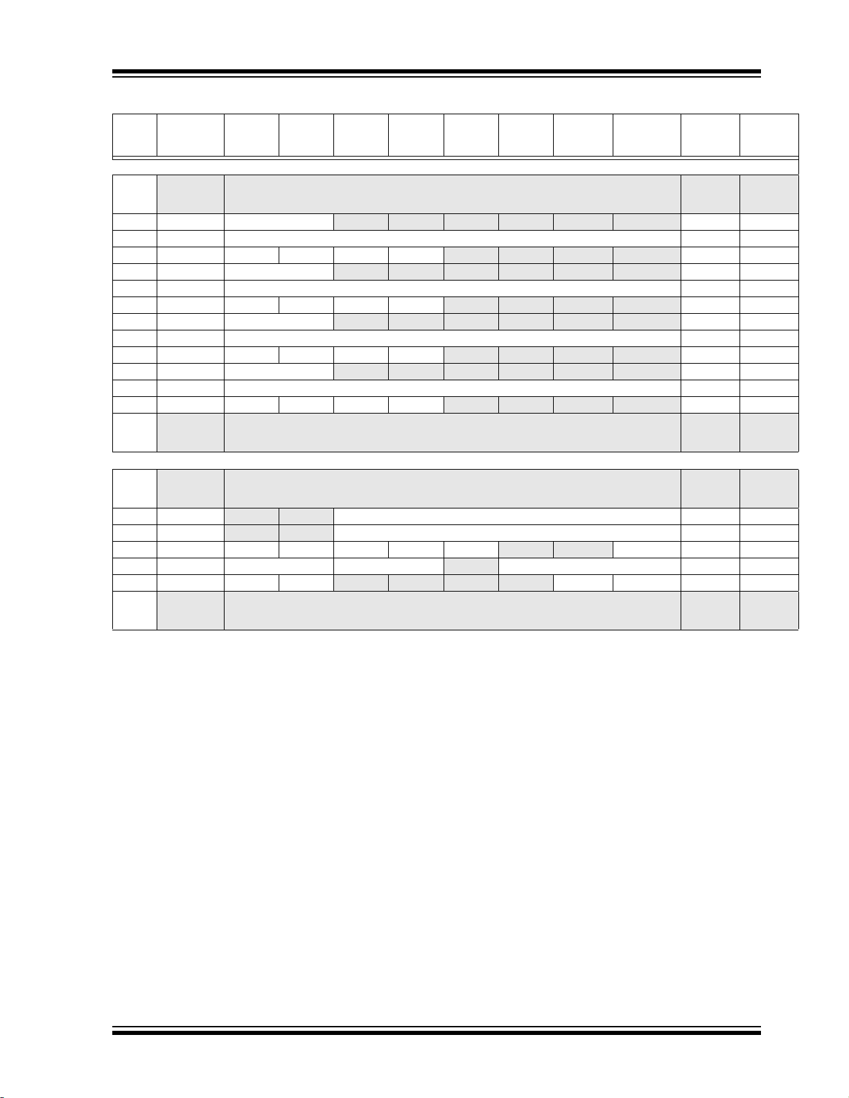
00Ch PORTA — — RA5 RA4 RA3 RA2 RA1 RA0 --xx xxxx --xx xxxx
00Dh PORTB RB7 RB6 RB5 RB4
00Eh PORTC RC7 RC6 RC5 RC4 RC3 RC2 RC1 RC0 xxxx xxxx xxxx xxxx
00Fh
010h
011h PIR1 TMR1GIF ADIF
012h PIR2
013h PIR3
014h
015h TMR0 Holding Register for the 8-bit Timer0 Count xxxx xxxx uuuu uuuu
016h TMR1L Holding Register for the Least Significant Byte of the 16-bit TMR1 Count xxxx xxxx uuuu uuuu
017h TMR1H Holding Register for the Most Significant Byte of the 16-bit TMR1 Count xxxx xxxx uuuu uuuu
018h T1CON TMR1CS<1:0> T1CKPS<1:0>
019h T1GCON TMR1GE T1GPOL T1GTM T1GSPM T1GGO/
01Ah TMR2 Timer2 Module Register 0000 0000 0000 0000
01Bh PR2 Timer2 Period Register 1111 1111 1111 1111
01Ch T2CON
01Dh
01Eh
01Fh
— Unimplemented — —
— Unimplemented — —
— — — — TMR2IF TMR1IF 00-- --00 00-- --00
— — — — — NCO1IF — — ---- -0-- ---- -0--
— — — — — — CLC2IF CLC1IF ---- --00 ---- --00
— Unimplemented — —
— T2OUTPS<3:0> TMR2ON T2CKPS<1:0> -000 0000 -000 0000
— Unimplemented — —
— Unimplemented — —
— Unimplemented — —
— — — — xxxx ---- xxxx ----
— T1SYNC —TMR1ON0000 -0-0 uuuu -u-u
DONE
T1GVAL —T1GSS0000 0x-0 uuuu ux-u
Bank 1
08Ch TRISA — — TRISA5 TRISA4 —
08Dh TRISB TRISB7 TRISB6 TRISB5 TRISB4
08Eh TRISC TRISC7 TRISC6 TRISC5 TRISC4 TRISC3 TRISC2 TRISC1 TRISC0 1111 1111 1111 1111
08Fh
090h
091h PIE1 TMR1GIE ADIE
092h PIE2
093h PIE3
094h
095h
096h PCON STKOVF STKUNF
097h WDTCON
098h
099h OSCCON
09Ah OSCSTAT
09Bh ADRESL A/D Result Register Low xxxx xxxx uuuu uuuu
09Ch ADRESH A/D Result Register High xxxx xxxx uuuu uuuu
09Dh ADCON0
09Eh ADCON1 ADFM ADCS<2:0>
09Fh ADCON2 TRIGSEL<3:0>
Legend: x = unknown, u = unchanged, q = value depends on condition, - = unimplemented, r = reserved.
Note 1: PIC16F1507 only.
— Unimplemented — —
— Unimplemented — —
— — — — TMR2IE TMR1IE 00-- --00 00-- --00
— — — — —NCO1IE — — ---- -0-- ---- -0--
— — — — — — CLC2IE CLC1IE ---- --00 ---- --00
— Unimplemented — —
OPTION_REG
— Unimplemented — —
Shaded locations are unimplemented, read as ‘0’.
2: Unimplemented, read as ‘1’.
WPUEN INTEDG TMR0CS TMR0SE PSA PS<2:0> 1111 1111 1111 1111
—RWDT RMCLR RI POR BOR 00-1 11qq qq-q qquu
— — WDTPS<4:0> SWDTEN --01 0110 --01 0110
— IRCF<3:0> —SCS<1:0>-011 1-00 -011 1-00
— — —HFIOFR— — LFIOFR HFIOFS 1-q0 --00 q-qq --qq
— CHS<4:0>
(2)
TRISA2 TRISA1 TRISA0 --11 1111 --11 1111
— — — — 1111 ---- 1111 ----
GO/DONE
— —
— — — — 0000 ---- 0000 ----
ADPREF<1:0>
ADON -000 0000 -000 0000
0000 --00 0000 --00
Value on all
other
Resets
DS41586A-page 25 Preliminary 2011 Microchip Technology Inc.
PIC16(L)F1507
TABLE 3-5: SPECIAL FUNCTION REGISTER SUMMARY (CONTINUED)
Address Name Bit 7 Bit 6 Bit 5 Bit 4 Bit 3 Bit 2 Bit 1 Bit 0
Value on
POR, BOR
Bank 2
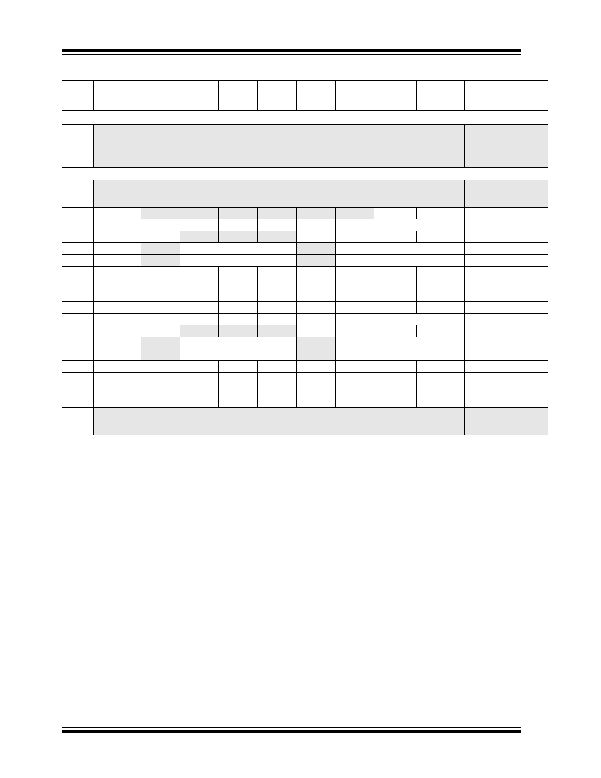
10Ch LATA — —LATA5LATA4— L ATA2 L ATA1 L ATA0 --xx -xxx --uu -uuu
10Dh LATB LATB7 LATB6 LATB5 LATB4
10Eh LATC LATC7 LATC6 LATC5 LATC4 LATC3 LATC2 LATC1 LATC0 xxxx xxxx uuuu uuuu
10Fh
to
— Unimplemented — —
115 h
116h BORCON SBOREN BORFS
117h FVRCON FVREN FVRRDY TSEN TSRNG
118 h
to
— Unimplemented — —
11C h
11Dh APFCON
11Eh
11Fh
— Unimplemented — —
— Unimplemented — —
— — — — — — CLC1SEL NCO1SEL ---- --00 ---- --00
— — — — — BORRDY 10-- ---q uu-- ---u
— — — — xxxx ---- uuuu ----
— —ADFVR<1:0>0q00 --00 0q00 --00
Bank 3
18Ch ANSELA — — — ANSA4 — ANSA2 ANSA1 ANSA0 ---1 -111 ---1 -111
18Dh ANSELB
18Eh ANSELC ANSC7 ANSC6
18Fh
190h
191h PMADRL Flash Program Memory Address Register Low Byte 0000 0000 0000 0000
192h PMADRH
193h PMDATL Flash Program Memory Read Data Register Low Byte xxxx xxxx uuuu uuuu
194h PMDATH
195h PMCON1
196h PMCON2 Flash Program Memory Control Register 2 0000 0000 0000 0000
197h VREGCON
— Unimplemented — —
— Unimplemented — —
198h
to
— Unimplemented — —
19Fh
— — ANSB5 ANSB4 — — — — --11 ---- --11 ----
— — ANSC3 ANSC2 ANSC1 ANSC0 11-- 1111 11-- 1111
— Flash Program Memory Address Register High Byte -000 0000 -000 0000
— — Flash Program Memory Read Data Register High Byte --xx xxxx --uu uuuu
(2)
—
(1)
——————VREGPMReserved ---- --01 ---- --01
CFGS LWLO FREE WRERR WREN WR RD 0000 x000 0000 q000
Bank 4
20Ch WPUA — — WPUA5 WPUA4 WPUA3 WPUA2 WPUA1 WPUA0 --11 1111 --11 1111
20Dh WPUB WPUB7 WPUB6 WPUB5 WPUB4
20Eh
to
— Unimplemented — —
21Fh
— — — — 1111 ---- 1111 ----
Bank 5
28Ch
— Unimplemented — —
to
29Fh
Bank 6
30Ch
to
— Unimplemented — —
31Fh
Legend: x = unknown, u = unchanged, q = value depends on condition, - = unimplemented, r = reserved.
Note 1: PIC16F1507 only.
Shaded locations are unimplemented, read as ‘0’.
2: Unimplemented, read as ‘1’.
Value on all
other
Resets
2011 Microchip Technology Inc. Preliminary DS41586A-page 26
PIC16(L)F1507
TABLE 3-5: SPECIAL FUNCTION REGISTER SUMMARY (CONTINUED)
Address Name Bit 7 Bit 6 Bit 5 B it 4 Bit 3 Bit 2 Bit 1 Bit 0
Bank 7
38Ch
— Unimplemented — —
to
390h
391h IOCAP
392h IOCAN
393h IOCAF
394h IOCBP IOCBP7 IOCBP6 IOCBP5 IOCBP4
395h IOCBN IOCBN7 IOCBN6 IOCBN5 IOCBN4
396h IOCBF IOCBF7 IOCBF6 IOCBF5 IOCBF4
397h
to
— Unimplemented — —
39Fh
— — IOCAP5 IOCAP4 IOCAP3
— — IOCAN5 IOCAN4 IOCAN3
— — IOCAF5 IOCAF4 IOCAF3
— — — — 0000 ---- 0000 ----
— — — — 0000 ---- 0000 ----
— — — — 0000 ---- 0000 ----
IOCAP2 IOCAP1 IOCAP0
IOCAN2 IOCAN1 IOCAN0
IOCAF2 IOCAF1 IOCAF0
Value on
POR, BOR
--00 0000 --00 0000
--00 0000 --00 0000
--00 0000 --00 0000
Bank 8
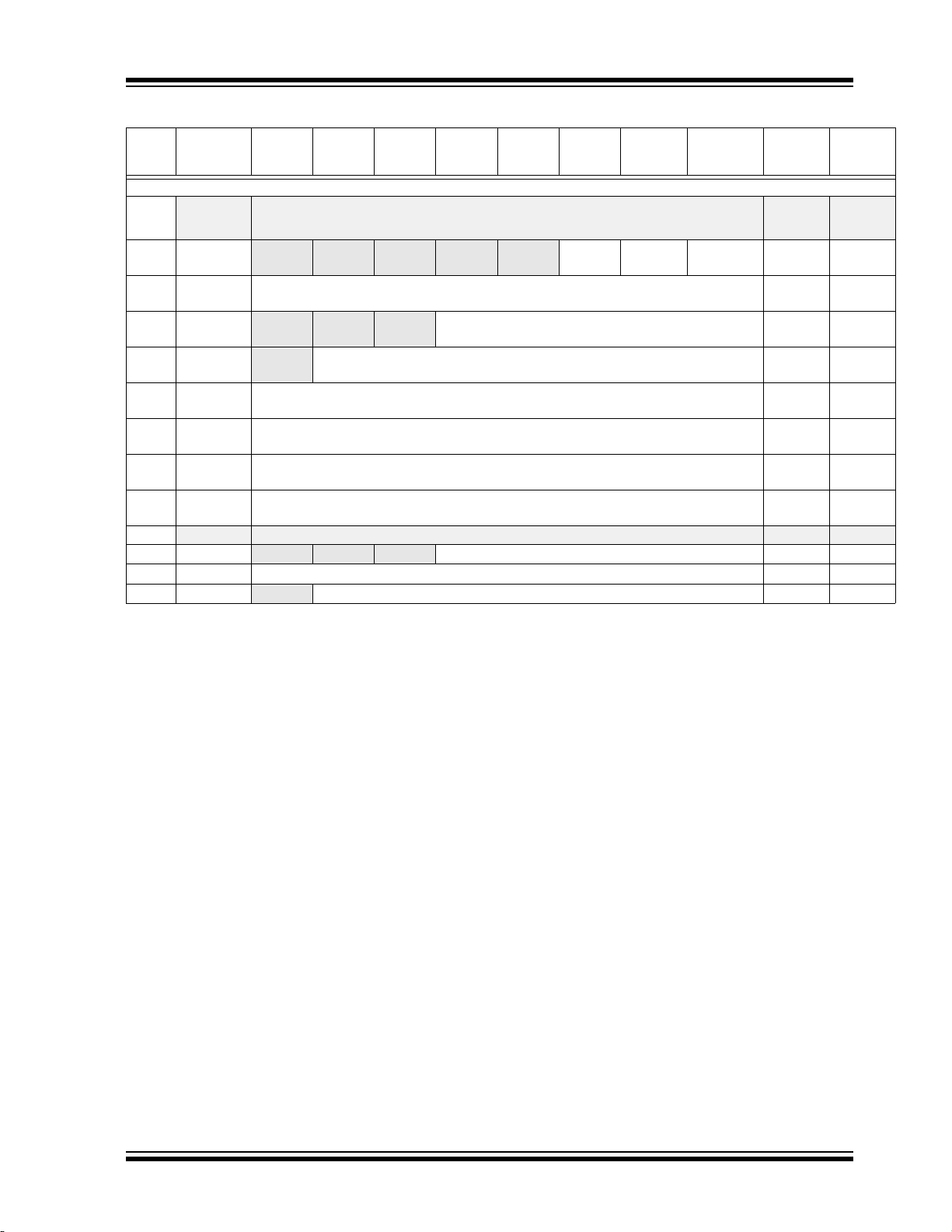
40Ch
— Unimplemented — —
to
41Fh
Bank 9
48Ch
to
— Unimplemented — —
497h
498h NCO1ACCL NCO1ACC<7:0> 0000 0000 0000 0000
499h NCO1ACCH NCO1ACC<15:8> 0000 0000 0000 0000
49Ah NCO1ACCU NCO1ACC<23:16> 0000 0000 0000 0000
49Bh NCO1INCL NCO1INC<7:0> 0000 0000 0000 0000
49Ch NCO1INCH NCO1INC<15:8> 0000 0000 0000 0000
49Dh
49Eh NCO1CON N1EN N1OE N1OUT N1POL
49Fh NCO1CLK N1PWS<2:0>
— Unimplemented — —
— — —N1PFM0000 ---0 0000 ---0
— — —N1CKS<1:0>0000 --00 0000 --00
Bank 10
50Ch
— Unimplemented — —
to
51Fh
Bank 11
58Ch
to
— Unimplemented — —
59Fh
Legend: x = unknown, u = unchanged, q = value depends on condition, - = unimplemented, r = reserved.
Note 1: PIC16F1507 only.
Shaded locations are unimplemented, read as ‘0’.
2: Unimplemented, read as ‘1’.
Value on all
other
Resets
DS41586A-page 27 Preliminary 2011 Microchip Technology Inc.
PIC16(L)F1507
TABLE 3-5: SPECIAL FUNCTION REGISTER SUMMARY (CONTINUED)
Address Name Bit 7 Bit 6 Bit 5 Bit 4 Bit 3 Bit 2 Bit 1 Bit 0
Bank 12
60Ch
— Unimplemented — —
to
610h
611h PWM1DCL PWM1DCL<7:6>
612h PWM1DCH PWM1DCH<7:0> xxxx xxxx uuuu uuuu
613h PWM1CON0 PWM1EN PWM1OE PWM1OUT PWM1POL
614h PWM2DCL PWM2DCL<7:6>
615h PWM2DCH PWM2DCH<7:0> xxxx xxxx uuuu uuuu
616h PWM2CON0 PWM2EN PWM2OE PWM2OUT PWM2POL
617h PWM3DCL PWM3DCL<7:6>
618h PWM3DCH PWM3DCH<7:0> xxxx xxxx uuuu uuuu
619h PWM3CON0 PWM3EN PWM3OE PWM3OUT PWM3POL
61Ah PWM4DCL PWM4DCL<7:6>
61Bh PWM4DCH PWM4DCH<7:0> xxxx xxxx uuuu uuuu
61Ch PWM4CON0 PWM4EN PWM4OE PWM4OUT PWM4POL
61Dh
to
— Unimplemented — —
61Fh
— — — — — — 00-- ---- 00-- ----
— — — — 0000 ---- 0000 ----
— — — — — — 00-- ---- 00-- ----
— — — — 0000 ---- 0000 ----
— — — — — — 00-- ---- 00-- ----
— — — — 0000 ---- 0000 ----
— — — — — — 00-- ---- 00-- ----
— — — — 0000 ---- 0000 ----
Value on
POR, BOR
Bank 13
68Ch
— Unimplemented — —
to
690h
691h CWG1DBR
692h CWG1DBF
693h CWG1CON0 G1EN G1OEB G1OEA G1POLB G1POLA
694h CWG1CON1 G1ASDLB<1:0> G1ASDLA<1:0>
695h CWG1ASD G1ASE G1ARSEN
696h
to
— Unimplemented — —
69Fh
Legend: x = unknown, u = unchanged, q = value depends on condition, - = unimplemented, r = reserved.
Note 1: PIC16F1507 only.
Shaded locations are unimplemented, read as ‘0’.
2: Unimplemented, read as ‘1’.
— —CWG1DBR<5:0>--00 0000 --00 0000
— —CWG1DBF<5:0>--xx xxxx --xx xxxx
— —G1CS00000 0--0 0000 0--0
— G1IS<2:0> 0000 -000 0000 -000
— — — — G1ASDSFLT G1ASDSCLC2 00-- --00 00-- --00
Value on all
other
Resets
2011 Microchip Technology Inc. Preliminary DS41586A-page 28
PIC16(L)F1507
TABLE 3-5: SPECIAL FUNCTION REGISTER SUMMARY (CONTINUED)
Address Name Bit 7 Bit 6 Bit 5 B it 4 Bit 3 Bit 2 Bit 1 Bit 0
Value on
POR, BOR
Banks 14-29
x0Ch/
x8Ch
—
x1Fh/
x9Fh
— Unimplemented — —
Bank 30
F0Ch
— Unimplemented — —
to
F0Eh
F0Fh CLCDATA
F10h CLC1CON LC1EN LC1OE LC1OUT LC1INTP LC1INTN LC1MODE<2:0> 0000 0000 0000 0000
F11h CLC1POL LC1POL
F12h CLC1SEL0
F13h CLC1SEL1
F14h CLC1GLS0 LC1G1D4T LC1G1D4N LC1G1D3T LC1G1D3N LC1G1D2T LC1G1D2N LC1G1D1T LC1G1D1N xxxx xxxx uuuu uuuu
F15h CLC1GLS1 LC1G2D4T LC1G2D4N LC1G2D3T LC1G2D3N LC1G2D2T LC1G2D2N LC1G2D1T LC1G2D1N xxxx xxxx uuuu uuuu
F16h CLC1GLS2 LC1G3D4T LC1G3D4N LC1G3D3T LC1G3D3N LC1G3D2T LC1G3D2N LC1G3D1T LC1G3D1N xxxx xxxx uuuu uuuu
F17h CLC1GLS3 LC1G4D4T LC1G4D4N LC1G4D3T LC1G4D3N LC1G4D2T LC1G4D2N LC1G4D1T LC1G4D1N xxxx xxxx uuuu uuuu
F18h CLC2CON LC2EN LC2OE LC2OUT LC2INTP LC2INTN LC2MODE<2:0> 0000 0000 0000 0000
F19h CLC2POL LC2POL
F1Ah CLC2SEL0
F1Bh CLC2SEL1
F1Ch CLC2GLS0 LC2G1D4T LC2G1D4N LC2G1D3T LC2G1D3N LC2G1D2T LC2G1D2N LC2G1D1T LC2G1D1N xxxx xxxx uuuu uuuu
F1Dh CLC2GLS1 LC2G2D4T LC2G2D4N LC2G2D3T LC2G2D3N LC2G2D2T LC2G2D2N LC2G2D1T LC2G2D1N xxxx xxxx uuuu uuuu
F1Eh CLC2GLS2 LC2G3D4T LC2G3D4N LC2G3D3T LC2G3D3N LC2G3D2T LC2G3D2N LC2G3D1T LC2G3D1N xxxx xxxx uuuu uuuu
F1Fh CLC2GLS3 LC2G4D4T LC2G4D4N LC2G4D3T LC2G4D3N LC2G4D2T LC2G4D2N LC2G4D1T LC2G4D1N xxxx xxxx uuuu uuuu
F20h
to
— Unimplemented — —
F6Fh
Legend: x = unknown, u = unchanged, q = value depends on condition, - = unimplemented, r = reserved.
Note 1: PIC16F1507 only.
Shaded locations are unimplemented, read as ‘0’.
2: Unimplemented, read as ‘1’.
— — — — — — PWM1POL PWM1POL ---- --00 ---- --00
— — — LC1G4POL LC1G3POL LC1G2POL LC1G1POL 0--- xxxx 0--- uuuu
— LC1D2S<2:0> — LC1D1S<2:0> -xxx -xxx -uuu -uuu
— LC1D4S<2:0> — LC1D3S<2:0> -xxx -xxx -uuu -uuu
— — — LC2G4POL LC2G3POL LC2G2POL LC2G1POL 0--- xxxx 0--- uuuu
— LC2D2S<2:0> — LC2D1S<2:0> -xxx -xxx -uuu -uuu
— LC2D4S<2:0> — LC2D3S<2:0> -xxx -xxx -uuu -uuu
Value on all
other
Resets
DS41586A-page 29 Preliminary 2011 Microchip Technology Inc.
PIC16(L)F1507
TABLE 3-5: SPECIAL FUNCTION REGISTER SUMMARY (CONTINUED)
Address Name Bit 7 Bit 6 Bit 5 Bit 4 Bit 3 Bit 2 Bit 1 Bit 0
Bank 31
F8Ch
—
FE3h
FE4h STATUS_
FE5h WREG_
FE6h BSR_
FE7h PCLATH_
FE8h FSR0L_
FE9h FSR0H_
FEAh FSR1L_
FEBh FSR1H_
FECh
FEDh
FEEh
FEFh
Legend: x = unknown, u = unchanged, q = value depends on condition, - = unimplemented, r = reserved.
Note 1: PIC16F1507 only.
— Unimplemented — —
— — — — — Z_SHAD DC_SHAD C_SHAD ---- -xxx ---- -uuu
SHAD
Working Register Shadow xxxx xxxx uuuu uuuu
SHAD
— — — Bank Select Register Shadow ---x xxxx ---u uuuu
SHAD
— Program Counter Latch High Register Shadow -xxx xxxx uuuu uuuu
SHAD
Indirect Data Memory Address 0 Low Pointer Shadow xxxx xxxx uuuu uuuu
SHAD
Indirect Data Memory Address 0 High Pointer Shadow xxxx xxxx uuuu uuuu
SHAD
Indirect Data Memory Address 1 Low Pointer Shadow xxxx xxxx uuuu uuuu
SHAD
Indirect Data Memory Address 1 High Pointer Shadow xxxx xxxx uuuu uuuu
SHAD
— Unimplemented — —
STKPTR
TOSL
TOSH
Shaded locations are unimplemented, read as ‘0’.
2: Unimplemented, read as ‘1’.
— — — Current Stack pointer ---1 1111 ---1 1111
Top-of-Stack Low byte xxxx xxxx uuuu uuuu
— Top-of-Stack High byte -xxx xxxx -uuu uuuu
Value on
POR, BOR
Value on all
other
Resets
2011 Microchip Technology Inc. Preliminary DS41586A-page 30
 Loading...