


PIC16F627A/628A/648A
Data Sheet
Flash-Based, 8-Bit CMOS
Microcontrollers with nanoWatt Technology
© 2007 Microchip Technology Inc. DS40044F

Note the following details of the code protection feature on Microchip devices:
• Microchip products meet the specification contained in their particular Microchip Data Sheet.
• Microchip believes that its family of products is one of the most secure families of its kind on the market today, when used in the
intended manner and under normal conditions.
• There are dishonest and possibly illegal methods used to breach the code protection feature. All of these methods, to our
knowledge, require using the Microchip products in a manner outside the operating specifications contained in Microchip’s Data
Sheets. Most likely, the person doing so is engaged in theft of intellectual property.
• Microchip is willing to work with the customer who is concerned about the integrity of their code.
• Neither Microchip nor any other semiconductor manufacturer can guarantee the security of their code. Code protection does not
mean that we are guaranteeing the product as “unbreakable.”
Code protection is constantly evolving. We at Microchip are committed to continuously improving the code protection features of our
products. Attempts to break Microchip’s code protection feature may be a violation of the Digit al Millennium Copyright Act. If suc h a c t s
allow unauthorized access to your software or other copyrighted work, you may have a right to sue for relief under that Act.
Information contained in this publication regarding device
applications and t he lik e is provided only for your convenience
and may be su perseded by upda t es . It is y our responsibility to
ensure that your application meets with your specifications.
MICROCHIP MAKES NO REPRESENTATIONS OR
WARRANTIES OF ANY KIND WHETHER EXPRESS OR
IMPLIED, WRITTEN OR ORAL, STATUTORY OR
OTHERWISE, RELATED TO THE INFORMATION,
INCLUDING BUT NOT LIMITED TO ITS CONDITION,
QUALITY, PERFORMANCE, MERCHANTABILITY OR
FITNESS FOR PURPOSE. Microchip disclaims all liability
arising from this information and its use. Use of Microchip
devices in life supp ort and/or safety ap plications is entir ely at
the buyer’s risk, and the buyer agrees to defend, indemnify and
hold harmless M icrochip from any and all dama ges, claims,
suits, or expenses re sulting from such use. No licens es are
conveyed, implicitly or otherwise, under any Microchip
intellectual property rights.
Trademarks
The Microchip name and logo, the Microchip logo, Accuron,
dsPIC, K
EELOQ, KEELOQ logo, microID, MPLAB, PIC,
PICmicro, PICSTART, PRO MATE, PowerSmart, rfPIC, an d
SmartShunt are registered trademarks of Microchip
Technology Incorporated in the U.S.A. and other countries.
AmpLab, FilterLab, Linear Active Thermistor, Migratable
Memory, MX DEV, MXLAB, PS logo, SEEVAL, SmartSensor
and The Embedded Control Solutions Company are
registered trademarks of Microchip Technology Incorporated
in the U.S.A.
Analog-for-the-Digital Age, Application Maestro, CodeGuard,
dsPICDEM, dsPICDEM.net, dsPICworks, ECAN,
ECONOMONITOR, FanSense, FlexROM, fuzzyLAB,
In-Circuit Serial Programming, ICSP, ICEPIC, Mindi, MiWi,
MPASM, MPLAB Certified logo, MPLIB, MPLINK, PICkit,
PICDEM, PICDEM.net, PICLAB, PICtail, PowerCal,
PowerInfo, PowerMate, PowerTool, REAL ICE, rfLAB,
rfPICDEM, Select Mode, Smart Serial, SmartT el, Total
Endurance, UNI/O, WiperLock and ZENA are trademarks of
Microchip Technology Incorporated in the U.S.A. and other
countries.
SQTP is a service mark of Microchip Technology Incorporated
in the U.S.A.
All other trademarks mentioned herein are property of their
respective companies.
© 2007, Microchip Technology Incorporated, Printed in the
U.S.A., All Rights Reserved.
Printed on recycled paper.
Microchip received ISO/TS-16949:2002 certification for its worldwide
headquarters, design and wafer fabrication facilities in Chandler and
Tempe, Arizona, Gresham, Oregon and Mountain View, California. The
Company’s quality system processes and procedures are for its PIC
MCUs and dsPIC® DSCs, KEELOQ
EEPROMs, microperipherals, nonvolatile memory and analog
products. In addition, Microchip’s quality system for the design and
manufacture of development systems is ISO 9001:2000 certified.
®
code hopping devices, Serial
DS40044F-page ii © 2007 Microchip Technology Inc.
®

PIC16F627A/628A/648A
18-pin Flash-Based, 8-Bit CMOS Microcontrollers
with nanoWatt Technology
High-Performance RISC CPU:
• Operating speeds from DC – 20 MHz
• Interrupt capability
• 8-level deep hardware stack
• Direct, Indirect and Relative Addressing modes
• 35 single-word instructions:
- All instructions single cycle except branches
Special Microcontroller Features:
• Internal and external oscilla tor opti ons :
- Precision internal 4MHz oscillator factory
calibrated to ±1%
- Low-power internal 48kHz oscillator
- External Oscillator support for crystals and
resonators
• Power-saving Sleep mode
• Programmable weak pull-u p s on PORTB
• Multiplexed Master Clear/In put -pin
• Watchdog Timer with independent osc illator for
reliable operation
• Low-voltage program mi ng
• In-Circuit Serial Programming™ (via two pins)
• Programmable code protection
• Brown-out Reset
• Power-on R eset
• Power-up Timer and Oscillator Start-up Timer
• Wide operating voltage range (2.0-5.5V)
• Industrial and extended temperature range
• High-Endurance Flash/EEPROM cell:
- 100,000 write Flash endurance
- 1,000,000 write EEPROM endurance
- 40 year data retention
Low-Power Features:
• Standby Current:
- 100 nA @ 2.0V, typical
• Operating Current:
-12μA @ 32 kHz, 2.0V, typical
-120μA @ 1 MHz, 2.0V, typical
• Watchdog Timer Current:
-1μA @ 2.0V, typical
• Timer1 Oscillator Current:
-1.2μA @ 32 kHz, 2.0V, typical
• Dual-speed Internal Oscillator:
- Run-time selectable betwe en 4MHz and
48 kHz
-4μs wake-up from Sleep, 3.0V, typical
Peripheral Features:
• 16 I/O pins with indiv idual direction control
• High current sink/source for direct LED drive
• Analog comparator module with:
- Two analog compara tors
- Programmable on-chip voltage reference
(V
REF) module
- Selectable internal or external reference
- Comparator outputs are externally accessible
• Timer0: 8-bit timer/counter with 8-bit
programmable prescaler
• Timer1: 16-bit timer/counter with external crystal/
clock capability
• Timer2: 8-bit timer/counter with 8-bit period
register, prescaler and postscaler
• Capture, Compare, PWM mo dul e:
- 16-bit Capture/Compare
-10-bit PWM
• Addressable Universal Synchronous/Asynchronous
Receiver/T ra nsmitt er USAR T/SCI
Program
Device
PIC16F627A 1024 224 128 16 1 Y 2 2/1
PIC16F628A 2048 224 128 16 1 Y 2 2/1
PIC16F648A 4096 256 256 16 1 Y 2 2/1
© 2007 Microchip Technology Inc. DS40044F-page 1
Memory
Flash
(words)
Data Memory
SRAM
(bytes)
EEPROM
(bytes)
I/O
CCP
(PWM)
USART Comparators
Timers
8/16-bit

PIC16F627A/628A/648A
Pin Diagrams
PDIP, SOIC
SSOP
RA2/AN2/V
RA3/AN3/CMP1
RA4/T0CKI/CMP2
RA5/MCLR
RA6/OSC2/CLKOUT
RA7/OSC1/CLKIN
VDD
RA1/AN1
RA0/AN0
19181615141312
20
PIC16F627A/628A/648A
2 3 4 5 6 7 8 910
1
REF
RA2/AN2/V
RA3/AN3/CMP1
VDD
RB6/T1OSO/T1CKI/PGC
RB7/T1OSI/PGD
17
SS
VSS
V
/VPP
RB0/INT
RB1/RX/DT
RA5/MCLR
RA4/T0CKI/CMP2
RB0/INT
RB1/RX/DT
RB2/TX/CK
RB3/CCP1
RB4/PGM
RB5
11
RB3/CCP1
RB2/TX/CK
REF
/VPP
VSS
118
27A/628A/648A
PIC16F627A/628A/648A
28-Pin
RB0/INT
17
16
15
14
13
12
11
10
QFN
VSS
VSS
2
3
4
5
6
7
8
9
RA5/MCLR/VPP
RA1/AN1
RA0/AN0
RA7/OSC1/CLKIN
RA6/OSC2/CLKOUT
DD
V
RB7/T1OSI/PGD
RB6/T1OSO/T1CKI/PGC
RB5
RB4/PGM
RA2/AN2/VREF
RA3/AN3/CMP1
RA4/T0CKI/CMP2
2827262524
1
NC
2
3
PIC16F627A/628A
NC
4
PIC16F648A
5
NC
6
7
8
9
10
RB3/CCP1
RB2/TX/CK
RB1/RX/DT
NC
11
NC
RA1/AN1
12
RB4/PGM
RA0/AN0
23
13
RB5
NC
22
21
20
19
18
17
16
15
14
NC
RA7/OSC1/CLKIN
RA6/OSC2/CLKOUT
V
DD
NC
VDD
RB7/T1OSI/PGD
RB6/T1OSO/T1CKI/PGC
DS40044F-page 2 © 2007 Microchip Technology Inc.

PIC16F627A/628A/648A
Table of Contents
1.0 General Description............................................................................ ....... .... .. .... .. .... .................................................................. 5
2.0 PIC16F627A/628A/648A Device Varieties.................................................................................................................................. 7
3.0 Architectural Overview................................................................................................................................................................ 9
4.0 Memory Organization................................................................................................................................................................ 15
5.0 I/O Ports................ .................................................................................................................................................................... 31
6.0 Timer0 Module .......................................................................................................................................................................... 45
7.0 Timer1 Module .......................................................................................................................................................................... 48
8.0 Timer2 Module .......................................................................................................................................................................... 52
9.0 Capture/Compare/PWM (CCP) Module .................................................................................................................................... 55
10.0 Comparator Module................................................................................................................................................................... 61
11.0 Voltage Reference Module........................................................................ .. .. .... .. .. .. .. ....... .. .. ..................................................... 67
12.0 Universal Synchronous Asynchronous Receiver Transmitter (USART) Module....................................................................... 7 1
13.0 Data EEPROM Memory................... ......................................................................................................................................... 89
14.0 Special Features of the CPU..................................... ................................................................................................................ 95
15.0 Instruction Set Summary......................................................................................................................................................... 115
16.0 Development Support.............................................................................................................................................................. 129
17.0 Electrical Specifications........................................................................................................................................................... 133
18.0 DC and AC Characteristics Graphs and Tables...................................................................................................................... 149
19.0 Packaging Information. .......................................................................................... .................................................................. 161
Appendix A: Revision History............................................................................................................................................................ 167
Appendix B: Device Differences ....................................................................................................................................................... 167
Appendix C: Device Migrations - PIC16C63/65A/73A/74A —> PIC16C63A/65B/73B/74B.............................................................. 168
Appendix D: Migration from Baseline to Mid-Range Devices ........................................................................................................... 168
The Microchip Web Site.................................................................................................................................................................... 169
Customer Change Notification Service ............................................................................................................................................. 169
Customer Support............................................................................................................................................................................. 169
Reader Response............................................................................................................................................................................. 170
Product Identification System........................................................................................................................................................... 175
TO OUR VALUED CUSTOMERS
It is our intention to provide our valued customers with t he best docume ntation possible to ensure successf ul use of your Mic rochip products. To this end, we will continue to improve our publications to better suit your needs. Our publications will be refined
and enhanced as new volumes and updates are introduced.
If you have any questions or comments regarding this publication, please contact the Marketing Communications Department via
E-mail at docerrors@microchip.com or fax the Reader Response Form in the back of this data sheet to (480) 792-4150. We
welcome your feedback.
Most Current Data Sheet
To obtain the most up-to-date version of this data sheet, please register at our Worldwide Web site at:
http://www.microchip.com
You can determine the version of a data sheet by examining its literature number found on the bottom outside corner of any page.
The last character of the literature number is the version number, (e.g., DS30000A is version A of document DS30000).
Errata
An errata sheet, describing minor operational differences from the data sheet and recommended workarounds, may exist for current
devices. As device/documentation issues become known to us, we will publish an errata sheet. The errata will specify the revision
of silicon and revision of document to which it applies.
To determine if an errata sheet exists for a particular device, please check with one of the following:
• Microchip’s Worldwide Web site; http://www.microchip.com
• Your local Microchip sales office (see last page)
When contacting a sales office, please specify which device, revision of silicon and data sheet (include literature number) you are
using.
Customer Notification System
Register on our web site at www.microchip.com to receive the most current information on all of our products.
© 2007 Microchip Technology Inc. DS40044F-page 3

PIC16F627A/628A/648A
NOTES:
DS40044F-page 4 © 2007 Microchip Technology Inc.

PIC16F627A/628A/648A
1.0 GENERAL DESCRIPTION
The PIC16F627A/628A/648A are 18-pin Flash-based
members of the versatile PIC16F627A/628A/648A
family of low-cost, high-performance, CMOS, fullystatic, 8-bit microcontrollers.
®
All PIC
architecture. The PIC16F627A/628A/648A have
enhanced core f eatures, a n eight-le vel dee p stac k, and
multiple internal and external interrupt sources. The
separate instruction and data buses of the Harvard
architecture allow a 14-bit wide instruction word with
the separate 8-bit wide data. The two-stage instruction
pipeline allows all instructions to execute in a singlecycle, except for program branche s (which require two
cycles). A to tal of 35 instruction s (reduced instr uction
set) are available, complemented by a large register
set.
PIC16F627A/628A/648A microcontrollers typically
achieve a 2:1 code compression and a 4:1 speed
improvement over other 8-bit microcontrollers in their
class.
PIC16F627A/628A/648A devices have integrated
features to reduce ex ternal com ponent s, th us redu cing
system cost, enha ncing system reliability an d re ducing
power consumption.
The PIC16F627A/628A/648A has 8 oscillator
configurations. The single-pin RC oscillator provides a
low-cost solution. The LP oscillator minimizes power
consumption, XT is a standard crystal, and INTOSC is
a self-contain ed precis ion two-spee d internal o scillator.
microcontrollers employ an advanced RISC
The HS mode is for High-Speed cryst als. The EC mode
is for an external clock source.
The Sleep (Power-down) mode offers power savings.
Users can wake-up the chip from Sleep through several
external interrupts, internal interrupts and Resets.
A highly reliable Watchdog Timer with its own on-chip
RC oscillator prov ides protection against softw are lockup.
Table 1-1 shows the features of the PIC16F627A/628A/
648A mid-range mi c r oc o n t ro l l e r f a m ily.
A simplified block diagram of the PIC16F627A/628A/
648A is shown in Figure 3-1.
The PIC16F627A/628A/648A se rie s fit s in app lic ati on s
ranging from battery chargers to low power remote
sensors. The Flash technology makes customizing
application programs (detection levels, pulse generation, timers, etc.) extremely fast and convenient. The
small footprint packages makes this microcontroller
series ideal for all applications with space limitations.
Low cost, low power, high performance, ease of use
and I/O flexibility make the PIC16F627A/628A/648A
very versatile.
1.1 Development Support
The PIC16F627A/628A/648A family is supported by a
full-featured macr o assemble r , a software simulato r , an
in-circuit emul ator, a l ow c os t i n-c irc ui t d ebu gger, a l ow
cost development programmer and a full-featured
programmer. A Third Party “C” compiler support tool is
also available.
T ABLE 1-1: PIC16F627A/628A/648A FAMILY OF DEVICES
PIC16F627A PIC16F628A PIC16F648A PIC16LF627A PIC16LF628A PIC16LF648A
Clock Maximum Frequency
Memory RAM Data Memory
Peripherals Capture/Compare/
Features Voltage Range (Volts) 3.0-5.5 3.0-5.5 3.0-5.5 2.0-5.5 2.0-5.5 2.0-5.5
All PIC
All PIC16F627A/628A/648A family devices use serial programming with clock pin RB6 and data pin RB7.
of Operation (MHz)
Flash Program
Memory (words)
(bytes)
EEPROM Data
Memory (bytes)
Timer module(s) TMR0, TMR1,
Comparator(s) 222222
PWM modules
Serial Communications USART USART USART USART USART USART
Internal Voltage
Reference
Interrupt Sources101010101010
I/O Pins 16 16 16 16 16 16
Brown-out Reset Yes Yes Yes Yes Yes Yes
Packages 18-pin DIP,
®
family devices have Power-on Reset, selectable Watchdog Timer, selectable code-protect and high I/O current capability.
20 20 20 20 20 20
1024 2048 4096 1024 2048 4096
224 224 256 224 224 256
128 128 256 128 128 256
TMR2
111111
Yes Yes Yes Yes Yes Yes
SOIC, 20-pin
SSOP,
28-pin QFN
TMR0, TMR1,
TMR2
18-pin DIP,
SOIC, 20-pin
SSOP,
28-pin QFN
TMR0, TMR1,
TMR2
18-pin DIP,
SOIC, 20-pin
SSOP,
28-pin QFN
TMR0, TMR1,
TMR2
18-pin DIP,
SOIC, 20-pin
SSOP,
28-pin QFN
TMR0, TMR1,
TMR2
18-pin DIP,
SOIC, 20-pin
SSOP,
28-pin QFN
TMR0, TMR1,
TMR2
18-pin DIP,
SOIC, 20-pin
SSOP,
28-pin QFN
© 2007 Microchip Technology Inc. DS40044F-page 5

PIC16F627A/628A/648A
NOTES:
DS40044F-page 6 © 2007 Microchip Technology Inc.

2.0 PIC16F627A/628A/648A DEVICE VARIETIES
A variety of frequency ranges and packaging options
are available. Depen ding on applicati on and production
requirements, t he proper devic e option can be s elected
using the information in the PIC16F627A/628A/648A
Product Identification System, at the end of this data
sheet. When placing orders, please use this page of
the data sheet to specify the correct part number.
2.1 Flash Devices
Flash devices can be erased and re-programmed
electrically. This allows the same devi ce to be used for
prototype develo pment, pil ot prog rams and prod uction.
A further advantage of t he electri cally erasab le Flash i s
that it can be erased a nd reprogrammed in-c ircuit, or by
device program mers, such as Mi crochip’s PIC START
Plus or PRO MATE® II programmers.
2.2 Quick-Turnaround-Production (QTP) Devices
PIC16F627A/628A/648A
®
Microchip offers a QTP Programming Service for
factory production orders. This service is made
available for users who chose not to program a medium
to high quantity o f un its and whose code patterns have
stabilized. T he devic es are st andard Flash dev ices, but
with all program locations and configuration options
already programmed by the factory. Certain code and
prototype verification procedures apply before
production shipments are available. Please contact
your Microchip Technology sales office for more
details.
2.3 Serialized Quick-TurnaroundProduction (SQTP
Microchip offers a unique programming service where
a few user-defined locations in each device are
programmed with different serial numbers. The serial
numbers may be random, pseudo-random or
sequential.
Serial programming allows each device to have a
unique number, which can serve as an entry-code,
password or ID number.
SM
) Devices
© 2007 Microchip Technology Inc. DS40044F-page 7

PIC16F627A/628A/648A
NOTES:
DS40044F-page 8 © 2007 Microchip Technology Inc.

PIC16F627A/628A/648A
3.0 ARCHITECTURAL OVERVIEW
The high performance of the PIC16F627A/628A/648A
family can be attributed to a number of architectural
features commonly fo und in RISC mic roproc esso rs. To
begin with, the PIC16F627A/628A/648A uses a
Harvard architecture in which program and data are
accessed from separate memories using separate
busses. This improves bandwidth over traditional Von
Neumann architecture where program and data are
fetched from the same memory. Separating program
and data memor y further allow s instructions to be sized
differently than 8-bit wide data word. Instruction
opcodes are 14-bits wide makin g it pos si ble to have all
single-word instructions. A 14-bit wide program memory access bus fetches a 14-bit instruction in a single
cycle. A two-stage pipeline overlaps fetch and execution of instructions. Consequently, all instructions (35)
execute in a single-cycle (200 ns @ 20 MHz) except for
program branches.
Table 3-1 lists device me mory sizes (Flash , Data and
EEPROM).
TABLE 3-1: DEVICE MEMORY LIST
Memory
Device
PIC16F627A 1024 x 14 224 x 8 128 x 8
PIC16F628A 2048 x 14 224 x 8 128 x 8
PIC16F648A 4096 x 14 256 x 8 256 x 8
PIC16LF627A 1024 x 14 224 x 8 128 x 8
PIC16LF628A 2048 x 14 224 x 8 128 x 8
PIC16LF648A 4096 x 14 256 x 8 256 x 8
Flash
Program
RAM
Data
EEPROM
Data
The PIC16F627A/628A/648A can directly or indirectly
address its register files or data memory. All Special
Function Registers (SFR), including the program
counter, are mapped in the data memory. The
PIC16F627A/628A/648A ha ve an orthogona l (symmetrical) instruction set that makes it possible to carry out
any operation, on any register, using any addressing
mode. This symmetrical nature and lack of ‘special
optimal situations’ makes programming with the
PIC16F627A/628A/648A simple yet efficient. In
addition, the learning curve is reduced significantly.
The PIC16F627A/628A/648A devices contain an 8-bit
ALU and working register. The ALU is a general
purpose arithmetic unit. It performs arithmetic and
Boolean functions be tween dat a in the work ing regist er
and any register file.
The ALU is 8-bits wide and capable of addition,
subtraction, shift and logical operations. Unless
otherwise me ntioned, arithmetic operations are two’s
complement in nature. In two-operand instructions,
typically one operand is the working register
(W register). The other operand is a file register or an
immediate const ant. In singl e operan d instru ction s, the
operand is either the W register or a file register.
The W register is an 8-bit workin g register used for ALU
operations. It is not an addressable register.
Depending on the instruction executed, the ALU may
affect the values of the Carry (C), Digit Carry (DC), and
Zero (Z) bits in the Status Register. The C and DC bits
operate as Borrow
respectively, in sub tractio n. See th e SUBLW and SUBWF
instructions for examples.
A simplified block diagram is shown in Figure 3-1, and
a description of the device pins in Table 3-2.
Two types of data memory are provided on the
PIC16F627A/628A/648A devices. Nonvolatile
EEPROM data memory is provided for long term
storage of data, such as calibration values, look-up
table data, and any other data which may require
periodic updating in the field. These data types are not
lost when power is removed. The other data memory
provided is regular RAM data memory. Regular RAM
data memory is provi de d for tempo r ary sto rage of data
during normal operation. Data is lost when power is
removed.
and Digit Borrow out bits,
© 2007 Microchip Technology Inc. DS40044F-page 9

PIC16F627A/628A/648A
FIGURE 3-1: BLOCK DIAGRAM
Program
Bus
OSC1/CLKIN
OSC2/CLKOUT
Flash
Program
Memory
14
Instruction Reg
Instruction
Decode &
Control
Timing
Generation
13
Program Counter
8-Level Stack
Direct Addr
8
Power-up
Oscillator
Start-up Timer
Power-on
Watchdog
Brown-out
Low-Voltage
Programming
(13-bit)
Timer
Reset
Timer
Reset
RAM Addr (1)
7
8
Data Bus
3
RAM
File
Registers
9
Addr MUX
8
FSR Reg
Status Re g
MUX
ALU
W Reg
8
Indirect
Addr
PORTA
PORTB
RA0/AN0
RA1/AN1
RA2/AN2/VREF
RA3/AN3/CMP1
RA4/T0CK1/CMP2
RA5/MCLR
RA6/OSC2/CLKOUT
RA7/OSC1/CLKIN
RB0/INT
RB1/RX/DT
RB2/TX/CK
RB3/CCP1
RB4/PGM
RB5
RB6/T1OSO/T1CKI/PGC
RB7/T1OSI/PGD
/VPP
MCLR
VDD, VSS
Comparator
VREF
Note 1: Higher order bits are from the Status register.
Timer0 Timer1 Timer2
CCP1
USART
Data EEPROM
DS40044F-page 10 © 2007 Microchip Technology Inc.

PIC16F627A/628A/648A
T ABLE 3-2: PIC16F627A/628A/648A PINOUT DESCRIPTION
Name Function Input Type Output Type Description
RA0/AN0 RA0 ST CMOS Bidirectional I/O port
AN0 AN — Analog comparator input
RA1/AN1 RA1 ST CMOS Bidirectional I/O port
AN1 AN — Analog comparator input
RA2/AN2/VREF RA2 ST CMOS Bidirectional I/O port
AN2 AN — Analog comparator input
REF —ANVREF output
V
RA3/AN3/CMP1 RA3 ST CMOS Bidirectional I/O port
AN3 AN — Analog comparator input
CMP1 — CMOS Comparator 1 output
RA4/T0CKI/CMP2 RA4 ST OD Bidirectional I/O port
T0CKI ST — Timer0 clock input
CMP2 — OD Comparator 2 output
RA5/MCLR
RA6/OSC2/CLKOUT RA6 ST CMOS Bidirectional I/O port
RA7/OSC1/CLKIN RA7 ST CMOS Bidirectional I/O port
RB0/INT RB0 TTL CMOS Bidirectional I/O port. Can be software
RB1/RX/DT RB1 TTL CMOS Bidirectional I/O port. Can be software
RB2/TX/CK RB2 TTL CMOS Bidirectional I/O port. Can be software
RB3/CCP1 RB3 TTL CMOS Bidirectional I/O port. Can be software
Legend: O = Output CMOS = CMOS Output P = Power
/VPP RA5 ST — Input port
MCLR
V
PP — — Programming voltage input
OSC2 — XTAL Oscillator crystal output. Connects to crystal
CLKOUT — CMOS In RC/INTOSC mode, OSC2 pin can output
OSC1 XTAL — Oscillator crystal input
CLKIN ST — External clock source input. RC biasing pin.
INT ST — External interrupt
RX ST — USART receive pin
DT ST CMOS Synchronous data I/O
TX — CMOS USART transmit pin
CK ST CMOS Synchronous clock I/O
CCP1 ST CMOS Capture/Compare/PWM I/O
— = Not used I = Input ST = Schmitt Trigger Input
TTL = TTL Input OD = Open Drain Output AN = Analog
ST — Master clear. When configu red as MCL R, this
pin is an active low Reset to the device.
Voltage on MCLR
during normal device operation.
or resonator in Crystal Oscillator mode.
CLKOUT, which has 1/4 the frequency of
OSC1.
programmed for internal weak pull-up.
programmed for internal weak pull-up.
programmed for internal weak pull-up.
programmed for internal weak pull-up.
/VPP must not exceed VDD
© 2007 Microchip Technology Inc. DS40044F-page 11

PIC16F627A/628A/648A
TABLE 3-2: PIC16F627A/628A/648A PINOUT DESCRIPTION (CONTINUED)
Name Function Input Type Output Type Description
RB4/PGM RB4 TTL CMOS Bidirectional I/O port. Interrupt-on-pin change.
Can be software programmed for internal
weak pull-up.
PGM ST — Low-voltage programming inp ut pin. When
low-voltage prog ram ming is enabl ed, the
interrupt-on-pin change and weak pull-up
resistor ar e disabled.
RB5 RB5 TTL CMOS Bidirectional I/O port. Interrupt-on-pin change.
Can be software programmed for internal
weak pull-up.
RB6/T1OSO/T1CKI/PGC RB6 TTL CMOS
T1OSO — XTAL Timer1 oscillator output
T1CKI ST — Timer1 clock input
PGC ST — ICSP™ programming clock
RB7/T1OSI/PGD RB7 TTL CMOS Bidirectional I/O port. Interrupt-on-pin change.
T1OSI XTAL — Timer1 oscillator input
PGD ST CMOS ICSP data I/O
SS VSS Power — Ground reference for logic and I/O pins
V
VDD VDD Power — Positive supply for logic and I/O pins
Legend: O = Output CMOS = CMOS Output P = Power
— = Not used I = Input ST = Schmitt Trigger Input
TTL = TTL Input OD = Open Drain Output AN = Analog
Bidirectional I/O port. Interrupt-on -pin change.
Can be software programmed for internal
weak pull-up.
Can be software programmed for internal
weak pull-up.
DS40044F-page 12 © 2007 Microchip Technology Inc.

PIC16F627A/628A/648A
l
3.1 Clocking Scheme/Instruction Cycle
The clock input (RA7/OSC1/CLKIN pin) is internally
divided by four to generate four non-overlapping
quadrature clocks namely Q1, Q2, Q3 and Q4.
Internally, the Program Counter (PC) is incremented
every Q1, the instruction is fetched from the program
memory and latched into the instruction register in Q4.
The instruction is decoded and executed during the
following Q1 through Q4. The clocks and instruction
execution flow is shown in Figure 3-2.
FIGURE 3-2: CLOCK/INSTRUCTION CYCLE
OSC1
Q1
Q2
Q3
Q4
PC
CLKOUT
Q1
Q2 Q3 Q4
PC PC + 1 PC + 2
Fetch INST (P C )
Execute INST (PC - 1) Fetch INST (PC + 1)
Q1
Q2 Q3 Q4
Execute INST (PC) Fetch INST (PC + 2)
3.2 Instruction Flow/Pipelining
An instruction cycle consists of four Q cycles (Q1, Q2,
Q3 and Q4). The instruction fetch and execute are
pipelined such that fetch takes one instruction cycle
while decode and execute takes another instruction
cycle. However, due to the pipelining, each instruction
effectively executes in one cycle. If an instruction
causes the program counter to change (e.g., GOTO)
then two cycles are req uired to c omplete the ins truction
(Example 3-1).
A fetch cycle begins with the program counter
incrementing in Q1.
In the execution cy cle, the fetch ed instruction i s latched
into the Instruction Register (IR) in cycle Q1. This
instruction is then decoded and executed during the
Q2, Q3 and Q4 c ycles. Dat a m emory is read during Q2
(operand read) and written during Q4 (destination
write).
Q1
Q2 Q3 Q4
Execute INST (PC + 1)
Interna
phase
clock
EXAMPLE 3-1: INSTRUCTION PIPELINE FLOW
1. MOVLW 55h Fetch 1 Execute 1
2. MOVWF PORTB Fetch 2 Execute 2
3. CALL SUB_1 Fetch 3 Execute 3
4. BSF PORTA, 3 Fetch 4
Note: All instructions are single cycle except for an y program branches. The se take two cycles since the fetch
instruction is “flushed” from th e pi peline while the new instruct io n is bei ng fetched and then execu t ed.
© 2007 Microchip Technology Inc. DS40044F-page 13
Flush
Fetch SUB_1 Execute SUB_1

PIC16F627A/628A/648A
NOTES:
DS40044F-page 14 © 2007 Microchip Technology Inc.

PIC16F627A/628A/648A
4.0 MEMORY ORGANIZATION
4.1 Program Memory Organization
The PIC16F627A/628A/648A has a 13-bit program
counter capable of addressing an 8K x 14 program
memory space. Only the first 1K x 14 (0000h-03FFh)
for the PIC16F627A, 2K x 14 (0000h-07FFh) for the
PIC16F628A and 4Kx 14 (0000h-0FFFh) for the
PIC16F648A are physically implemented. Accessing a
location above these boundaries will cause a wraparound within the first 1K x 14 space (PIC16F627A),
2K x 14 space (PIC16F628A) or 4K x 14 space
(PIC16F648A). The Reset vector is at 0000h and the
interrupt vector is at 0004h (Figure 4-1).
FIGURE 4-1: PROGRAM MEMORY MAP
AND STACK
PC<12:0>
CALL, RETURN
RETFIE, RETLW
Stack Level 1
Stack Level 2
13
4.2 Data Memory Organization
The data memory (Figure 4-2 and Figure 4-3) is
partitioned into four banks, which contain the General
Purpose Registers (GPRs) and the Special Function
Registers (SFRs). The SFRs are located in the first 32
locations of each bank. There are General Purpose
Registers implemented as static RAM in each bank.
Table 4-1 lists the General Purpose Register available
in each of the four banks.
TABLE 4-1: GENERAL PURPOSE STATIC
RAM REGISTERS
PIC16F627A/628A PIC16F648A
Bank0 20-7Fh 20-7Fh
Bank1 A0h-FF A0h-FF
Bank2 120h-14Fh, 170h-17Fh 120h-17Fh
Bank3 1F0h-1FFh 1F0h-1FFh
Addresses F0h-FFh, 170h-17Fh and 1F0h-1FFh are
implemented as common RAM and mapped back to
addresses 70h-7Fh.
T abl e 4-2 lists how to acces s the four banks of regis ters
via the Status register bits RP1 and RP0.
Stack Level 8
Reset Vector
Interru pt Vector
On-chip Program
Memory
PIC16F627A,
PIC16F628A and
PIC16F648A
On-chip Program
Memory
PIC16F628A and
PIC16F648A
On-chip Program
Memory
PIC16F648A only
000h
0004
0005
03FFh
07FFh
0FFFh
TABLE 4-2: ACCESS TO BANKS OF
REGISTERS
Bank RP1 RP0
0 00
1 01
2 10
3 11
4.2.1 GENERAL PURPOSE REGISTER FILE
The register file is organized as 224 x 8 in the
PIC16F627A/628A and 256 x 8 in the PIC16F648A.
Each is accessed either directly or indirectly through
the File Select Register (FSR), See Section 4.4
“Indirect Addressing, INDF and FSR Registers”.
1FFFh
© 2007 Microchip Technology Inc. DS40044F-page 15

PIC16F627A/628A/648A
FIGURE 4-2: DATA MEMORY MAP OF THE PIC16F627A AND PIC16F628A
File
Address
Indirect addr.
TMR0
PCL
STATUS
FSR
PORTA
PORTB
PCLATH
INTCON
PIR1
TMR1L
TMR1H
T1CON
TMR2
T2CON
CCPR1L
CCPR1H
CCP1CON
RCSTA
TXREG
RCREG
CMCON
General
Purpose
Register
80 Bytes
16 Bytes
Bank 0
(1)
00h
01h
02h
03h
04h
05h
06h
07h
08h
09h
0Ah
0Bh
0Ch
0Dh
0Eh
0Fh
10h
11h
12h
13h
14h
15h
16h
17h
18h
19h
1Ah
1Bh
1Ch
1Dh
1Eh
1Fh
20h
6Fh
70h
7Fh FFh
Indirect addr.
OPTION
PCL
STATUS
FSR
TRISA
TRISB
PCLATH
INTCON
PIE1
PCON
PR2
TXSTA
SPBRG
EEDATA
EEADR
EECON1
EECON2
VRCON
General
Purpose
Register
80 Bytes
accesses
70h-7Fh
Bank 1
PCL
FSR
TRISB
(1)
180h
181h
182h
183h
184h
185h
186h
187h
188h
189h
18Ah
18Bh
18Ch
18Dh
18Eh
18Fh
1EFh
1F0h
TMR0
PCL
FSR
(1)
100h
101h
102h
103h
104h
105h
106h
107h
108h
109h
10Ah
10Bh
10Ch
10Dh
10Eh
10Fh
11Fh
120h
14Fh
150h
16Fh
170h
17Fh 1FFh
Indirect addr.
OPTION
STATUS
PCLATH
INTCON
accesses
70h-7Fh
Bank 3
(1)
80h
81h
82h
83h
84h
85h
86h
87h
88h
89h
8Ah
8Bh
8Ch
8Dh
8Eh
8Fh
90h
91h
92h
93h
94h
95h
96h
97h
98h
99h
9Ah
9Bh
9Ch
(1)
9Dh
9Eh
9Fh
A0h
EFh
F0h
Indirect addr.
STATUS
PORTB
PCLATH
INTCON
General
Purpose
Register
48 Bytes
accesses
70h-7Fh
Bank 2
Note 1: Not a physical register.
DS40044F-page 16 © 2007 Microchip Technology Inc.
Unimplemented data memory locations, read as ‘0’.

PIC16F627A/628A/648A
FIGURE 4-3: DATA MEMORY MAP OF THE PIC16F648A
File
Address
Indirect addr.
TMR0
PCL
STATUS
FSR
PORTA
PORTB
PCLATH
INTCON
PIR1
TMR1L
TMR1H
T1CON
TMR2
T2CON
CCPR1L
CCPR1H
CCP1CON
RCSTA
TXREG
RCREG
CMCON
General
Purpose
Register
80 Bytes
16 Bytes
Bank 0
(1)
00h
01h
02h
03h
04h
05h
06h
07h
08h
09h
0Ah
0Bh
0Ch
0Dh
0Eh
0Fh
10h
11h
12h
13h
14h
15h
16h
17h
18h
19h
1Ah
1Bh
1Ch
1Dh
1Eh
1Fh
20h
6Fh
70h
7Fh FFh
Indirect addr.
OPTION
PCL
STATUS
FSR
TRISA
TRISB
PCLATH
INTCON
PIE1
PCON
PR2
TXSTA
SPBRG
EEDATA
EEADR
EECON1
EECON2
VRCON
General
Purpose
Register
80 Bytes
accesses
70h-7Fh
Bank 1
PCL
FSR
TRISB
(1)
180h
181h
182h
183h
184h
185h
186h
187h
188h
189h
18Ah
18Bh
18Ch
18Dh
18Eh
18Fh
1EFh
1F0h
TMR0
PCL
FSR
(1)
100h
101h
102h
103h
104h
105h
106h
107h
108h
109h
10Ah
10Bh
10Ch
10Dh
10Eh
10Fh
11Fh
120h
16Fh
170h
17Fh 1FFh
Indirect addr.
OPTION
STATUS
PCLATH
INTCON
accesses
70h-7Fh
Bank 3
(1)
80h
81h
82h
83h
84h
85h
86h
87h
88h
89h
8Ah
8Bh
8Ch
8Dh
8Eh
8Fh
90h
91h
92h
93h
94h
95h
96h
97h
98h
99h
9Ah
9Bh
9Ch
(1)
9Dh
9Eh
9Fh
A0h
EFh
F0h
Indirect addr.
STATUS
PORTB
PCLATH
INTCON
General
Purpose
Register
80 Bytes
accesses
70h-7Fh
Bank 2
Note 1: Not a physical register.
© 2007 Microchip Technology Inc. DS40044F-page 17
Unimplemented data memory locations, read as ‘0’.

PIC16F627A/628A/648A
4.2.2 SPECIAL FUNCTION REGISTERS
The SFRs are registers used by the CPU and Peripheral functions for controlling the desired operation of
the device (Table4-3). These registers are st a tic RAM.
The special registers can be classified into two sets
(core and peripheral). The SFRs associated with the
“core” functions are described in this section. Those
related to the operation of the peripheral features are
described in the section of that peripheral feature.
TABLE 4-3: SPECIAL REGISTERS SUMMARY BANK0
Address Name Bit 7 Bit 6 Bit 5 Bit 4 Bit 3 Bit 2 Bit 1 Bit 0
Bank 0
00h INDF Addressing this location uses contents of FSR to address data memory (not a physical register) xxxx xxxx 28
01h TMR0 Timer0 Module’s Register xxxx xxxx 45
02h PCL Program Counter’s (PC) Least Significant Byte 0000 0000 28
03h STATUS IRP RP1 RP0 TO
04h F SR Indirect Data Memory Ad dr ess Pointer xxxx xxxx 28
05h PORTA
06h PORTB RB7 RB6 RB5 RB4 RB3 RB2 RB1 RB0 xxxx xxxx 36
07h — Unimplemented — —
08h — Unimplemented — —
09h — Unimplemented — —
0Ah PCLATH — — — Write Buffer for upper 5 bits of Program Counter ---0 0000 28
0Bh INTCON GIE PEIE T0IE INTE RBIE T0IF INTF RBIF 0000 000x 24
0Ch PIR1
0Dh — Unimplemented — —
0Eh TMR1L Holding Register for the Least Significant Byte of the 16-bit TMR1 Register xxxx xxxx 48
0Fh TMR1H Holding Register for the Most Significant Byte of the 16-bit TMR1 Register xxxx xxxx 48
10h T1CON
11h TMR2 TMR2 Module’s Register 0000 0000 52
12h T2CON
13h — Unimplemented — —
14h — Unimplemented — —
15h CCPR1L Capture/Compare/PWM Register (LSB) xxxx xxxx 55
16h CCPR1H Capture/Compare/PWM Register (MSB) xxxx xxxx 55
17h CCP1CON
18h RCSTA SPEN RX9 SREN CREN ADEN FERR OERR RX9D 0000 000x 72
19h TXREG USART Transmit Data Register 0000 0000 77
1Ah RCREG USART Receive Data Register 0000 0000 80
1Bh — Unimplemented — —
1Ch — Unimplemented — —
1Dh — Unimplemented — —
1Eh — Unimplemented — —
1Fh CMCON C2OUT C1OUT
Legend: - = Unimplemented locations read as ‘0’, u = unchanged, x = unknown, q = value depends on condition, shaded = unimplemented
Note 1: For the initialization condition for registers tables, refer to Table 14-6 and Table 14-7.
RA7 RA6 RA5 RA4 RA3 RA2 RA1 RA0 xxxx 0000 31
EEIF CMIF RCI F TXIF — CCP1IF TMR2IF TMR1IF 0000 -000 26
— — T1CKPS1 T1CKPS0 T1OSCEN T1SYNC TMR1CS TMR1ON --00 0000 48
— TOUTPS3 TOUTPS2 TOUTPS1 TOUTPS0 TMR2ON T2CKPS1 T2CKPS0 -000 0000 52
— — CCP1X CCP1Y CCP1M3 CCP1M2 CCP1M1 CCP1M0 --00 0000 55
C2INV C1INV CIS CM2 CM1 CM0 0000 0000 61
PD ZDCC0001 1xxx 22
Value on
POR
Reset
Details
on Page
(1)
DS40044F-page 18 © 2007 Microchip Technology Inc.

PIC16F627A/628A/648A
TABLE 4-4: SPECIAL FUNCTION REGISTERS SUMMARY BANK1
Address Name Bit 7 Bit 6 Bit 5 Bit 4 Bit 3 Bit 2 Bit 1 Bit 0
Bank 1
80h INDF Addressing this location uses contents of FSR to address data memory (not a physical
81h OPTION RBPU
82h PCL Program Counter’s (PC) Least Significant Byte 0000 0000 28
83h STATUS IRP RP1 RP0 TO
84h FSR Indirect Data Memory Address Pointer xxxx xxxx 28
85h TRISA TRISA7 TRISA6 TRISA5 TRISA4 TRISA3 TRISA2 TRISA1 TRISA0 1111 1111 31
86h TRISB TRISB7 TRISB6 TRISB5 TRISB4 TRISB3 TRISB2 TRISB1 TRISB0 1111 1111 36
87h — Unimplemented — —
88h — Unimplemented — —
89h — Unimplemented — —
8Ah PCLATH
8Bh INTCON GIE PEIE T0IE INTE RBIE T0IF INTF RBIF 0000 000x 24
8Ch PIE1 EEIE CMIE RCIE TXIE
8Dh — Unimplemented — —
8Eh PCON
8Fh — Unimplemented — —
90h — Unimplemented — —
91h — Unimplemented — —
92h PR2 Timer2 Period Register 1111 1111 52
93h — Unimplemented — —
94h — Unimplemented — —
95h — Unimplemented — —
96h — Unimplemented — —
97h — Unimplemented — —
98h TXSTA CSRC TX9 TXEN SYNC
99h SPBRG Baud Rate Generator Register 0000 0000 73
9Ah EEDATA EEPROM Data Register xxxx xxxx 89
9Bh EEADR EEPROM Address Register xxxx xxxx 90
9Ch EECON1
9Dh EECON2 EEPROM Control Register 2 (not a physical register) ---- ---- 90
9Eh — Unimplemented — —
9Fh VRCON VREN VROE VRR
Legend: - = Unimplemented locations read as ‘0’, u = unchanged, x = unknown, q = value depends on condition, shaded = unimplemented
Note 1: For the initialization condition for registers tables, refer to Table 14-6 and Table 14-7.
register)
INTEDG T0CS T0SE PSA PS2 PS1 PS0 1111 1111 23
PD ZDCC0001 1xxx 22
— — — Write Buffer for upper 5 bits of Program Counter ---0 0000 28
— CCP1IE TMR2IE TMR1IE 0000 -000 25
— — — — OSCF —PORBOR ---- 1-0x 27
— BRGH TRMT TX9D 0000 -010 71
— — — — WRERR WREN WR RD ---- x000 90
— VR3 VR2 VR1 VR0 000- 0000 67
Value on
POR
Reset
xxxx xxxx 28
Details
on Page
(1)
© 2007 Microchip Technology Inc. DS40044F-page 19

PIC16F627A/628A/648A
TABLE 4-5: SPECIAL FUNCTION REGISTERS SUMMARY BANK2
Address Name Bit 7 Bit 6 Bit 5 Bit 4 Bit 3 Bit 2 Bit 1 Bit 0
Bank 2
100h INDF Addressing this location uses contents of FSR to address data memory (not a physical register) xxxx xxxx 28
101h TMR0
102h PCL Program Counter’s (PC) Least Significant Byte 0000 0000 28
103h STATUS IRP RP1 RP0 TO
104h FSR Indirect Data Memory Address Pointer xxxx xxxx 28
105h — Unimplemented — —
106h PORTB RB7 RB6 RB5 RB4 RB3 RB2 RB1 RB0 xxxx xxxx 36
107h — Unimplemented — —
108h — Unimplemented — —
109h — Unimplemented — —
10Ah PCLATH
10Bh INTCON GIE PEIE T0IE INTE RBIE T0IF INTF RBIF 0000 000x 24
10Ch — Unimplemented — —
10Dh — Unimplemented — —
10Eh — Unimplemented — —
10Fh — Unimplemented — —
110h — Unimplemented — —
111h — Unimplemented — —
112h — Unimplemented — —
113h — Unimplemented — —
114h — Unimplemented — —
115h — Unimplemented — —
116h — Unimplemented — —
117h — Unimplemented — —
118h — Unimplemented — —
119h — Unimplemented — —
11Ah — Unimplemented — —
11Bh — Unimplemented — —
11Ch — Unimplemented — —
11Dh — Unimplemented — —
11Eh — Unimplemented — —
11Fh — Unimplemented — —
Legend: - = Unimplemented locations read as ‘0’, u = unchanged, x = unknown, q = value depends on condition, shaded = unimplemented.
Note 1: For the initialization condition for registers tables, refer to Table 14-6 and Table 14-7.
Timer0 Module’s Register xxxx xxxx
PD ZDCC0001 1xxx 22
— — — Write Buffer for upper 5 bits of Program Counter ---0 0000 28
Value on
POR
Reset
Details
on Page
(1)
45
DS40044F-page 20 © 2007 Microchip Technology Inc.

PIC16F627A/628A/648A
TABLE 4-6: SPECIAL FUNCTION REGISTERS SUMMARY BANK3
Address Name Bit 7 Bit 6 Bit 5 Bit 4 Bit 3 Bit 2 Bit 1 Bit 0
Bank 3
180h INDF Addressing this location uses contents of FSR to address data memory (not a physical register) xxxx xxxx 28
181h OPTION RBPU
182h PCL Program Counter’s (PC) Least Significant Byte 0000 0000 28
183h STATUS IRP RP1 RP0 TO
184h FSR Indirect Data Memory Address Pointer xxxx xxxx 28
185h — Unimplemented — —
186h TRISB TRISB7 TRISB6 TRISB5 TRISB4 TRISB3 TRISB2 TRISB1 TRISB0 1111 1111 36
187h — Unimplemented — —
188h — Unimplemented — —
189h — Unimplemented — —
18Ah PCLATH
18Bh INTCON GIE PEIE T0IE INTE RBIE T0IF INTF RBIF 0000 000x 24
18Ch — Unimplemented — —
18Dh — Unimplemented — —
18Eh — Unimplemented — —
18Fh — Unimplemented — —
190h — Unimplemented — —
191h — Unimplemented — —
192h — Unimplemented — —
193h — Unimplemented — —
194h — Unimplemented — —
195h — Unimplemented — —
196h — Unimplemented — —
197h — Unimplemented — —
198h — Unimplemented — —
199h — Unimplemented — —
19Ah — Unimplemented — —
19Bh — Unimplemented — —
19Ch — Unimplemented — —
19Dh — Unimplemented — —
19Eh — Unimplemented — —
19Fh — Unimplemented — —
Legend: - = Unimplemented locations read as ‘0’, u = unchanged, x = unknown, q = value depends on condition, shaded = unimplemented
Note 1: For the initialization condition for registers tables, refer to Table 14-6 and Table 14-7.
INTEDG T0CS T0SE PSA PS2 PS1 PS0 1111 1111 23
PD ZDCC0001 1xxx 22
— — — Write Buffer for upper 5 bits of Program Counter ---0 0000 28
Value on
POR
Reset
Details
on Page
(1)
© 2007 Microchip Technology Inc. DS40044F-page 21

PIC16F627A/628A/648A
4.2.2.1 Status Register
The St atus register , s hown in Register4-1, contains th e
arithmeti c statu s of th e ALU; the Re set sta tus an d the
bank select bits for data memory (SRAM).
The Status register can be the destination for any
instruction, like any other register. If the Status register
is the destination for an instruction that affects the Z,
DC or C bits, then the write to these three bits is
disabled. These bit s are set or cleared ac cording to the
device logic. Further more, the T O
writable. Therefore, the result of an instruction with the
Status register as destination may be different than
intended.
and PD bits are non-
For example, CLRF STATUS will clear the upper-three
bits and set the Z bit. This leaves the Status register
as “000uu1uu” (where u = unchanged).
It is recommended, therefore, that only BCF, BSF,
SWAPF and MOVWF instructions are used to alter the
Stat us register be cause the se instruct ions do not af fect
any Status bit. For other instructions, not affecting any
Status bits, see the “Instruction Set Summary”.
Note: The C and DC bits operate as a Borrow
and Digit Borrow out bit, respectively, in
subtraction. See the SUBLW and SUBWF
instructions for examples.
REGISTER 4-1: STATUS – STATUS REGISTER (ADDRESS: 03h, 83h, 103h, 183h)
R/W-0 R/W-0 R/W-0 R-1 R-1 R/W-x R/W-x R/W-x
IRP RP1 RP0 TO
bit 7 bit 0
bit 7 IRP: Register Bank Select bit (used for indirect addressing)
1 = Bank 2, 3 (100h-1FFh)
0 = Bank 0, 1 (00h-FFh)
bit 6-5 RP<1:0>: Register Bank Select bits (used for direct addressing)
00 = Bank 0 (00h-7Fh)
01 = Bank 1 (80h-FFh)
10 = Bank 2 (100h-17Fh)
11 = Bank 3 (180h-1FFh)
bit 4 TO
bit 3 PD
bit 2 Z: Zero bit
bit 1 DC: Digit Carry/Bo
bit 0 C: Carry/Bo
: Time Out bit
1 = After power-up, CLRWDT instruction or SLEEP instruction
0 = A WDT time out occurred
: Power-down bit
1 = After power-up or by the CLRWDT instruction
0 = By execution of the SLEEP instruction
1 = The result of an arithmetic or logic operation is zero
0 = The result of an arithmetic or logic operation is not zero
rrow bit (ADDWF, ADDLW,SUBLW,SUBWF instructions) (for Borrow the polarity
is reversed)
1 = A carry-out from the 4th low order bit of the result occurred
0 = No carry-out from the 4th low order bit of the result
rrow bit (ADDWF, ADDLW,SUBLW,SUBWF instructions)
1 = A carry-out from the Most Significant bit of the result occurred
0 = No carry-out from the Most Significant bit of the result occurred
Note: For Bo
rrow, the polarity is reversed. A subtraction is executed by adding the two’s
complement of the second operand. For rotate (RRF, RLF) instructions, this bit is
loaded with either the high or low order bit of the source register.
PD ZDCC
Legend:
R = Readable bit W = Writable bit U = Unimplemented bit, read as ‘0’
-n = Value at POR ‘1’ = Bit is set ‘0’ = Bit is cleared x = Bit is unknown
DS40044F-page 22 © 2007 Microchip Technology Inc.

PIC16F627A/628A/648A
4.2.2.2 OPTION Register
The Option register is a readable and writable register,
which contains various control bits to configure the
TMR0/WDT prescaler, the external RB0/INT interrupt,
TMR0 and the weak pull-ups on PORTB.
REGISTER 4-2: OPTION_REG – OPTION REGISTER (ADDRESS: 81h, 181h)
R/W-1 R/W-1 R/W-1 R/W-1 R/W-1 R/W-1 R/W-1 R/W-1
RBPU
bit 7 bit 0
INTEDG T0CS T0SE PSA PS2 PS1 PS0
Note: To achieve a 1:1 prescaler assignment for
TMR0, assign the prescaler to the WDT
(PSA = 1). See Section 6.3.1 “Switching
Prescaler Assignment”.
bit 7 RBPU
bit 6 INTEDG: Interrupt Edge Select bit
bit 5 T0CS: TMR0 Clock Source Select bit
bit 4 T0SE: TMR0 Source Edge Select bit
bit 3 PSA: Prescaler Assignment bit
bit 2-0 PS<2:0>: Prescaler Rate Select bits
: PORTB Pull-up Enable bit
1 = PORTB pull-ups are disabled
0 = PORTB pull-ups are enabled by individual port latch values
1 = Interrupt on rising edge of RB0/INT pin
0 = Interrupt on falling edge of RB0/INT pin
1 = Transition on RA4/T0CKI/CMP2 pin
0 = Internal instruction cycle clock (CLKOUT)
1 = Increment on high-to-low transition on RA4/T0CKI/CMP2 pin
0 = Increment on low-to-high transition on RA4/T0CKI/CMP2 pin
1 = Prescaler is assigned to the WDT
0 = Prescaler is assigned to the Timer0 module
Bit Value TMR0 Rate WDT Rate
000
001
010
011
100
101
110
111
1 : 2
1 : 4
1 : 8
1 : 16
1 : 32
1 : 64
1 : 128
1 : 256
1 : 1
1 : 2
1 : 4
1 : 8
1 : 16
1 : 32
1 : 64
1 : 128
Legend:
R = Readable bit W = Writable bit U = Unimplemented bit, read as ‘0’
-n = Value at POR ‘1’ = Bit is set ‘0’ = Bit is cleared x = Bit is unknown
© 2007 Microchip Technology Inc. DS40044F-page 23

PIC16F627A/628A/648A
4.2.2.3 INTCON Register
The INTCON register is a readable and writable
register , which c ontains the various en able and fl ag bit s
for all interrupt so urces excep t th e comp arator mo dule.
See Section 4.2.2.4 “PIE1 Register” and
Section 4.2.2.5 “PIR1 Register” for a description of
the comparator enable and flag bits.
Note: Interrupt flag bits get set when an interrupt
condition occurs regard less of the sta te of
its corresponding enable bit or the global
enable bit, GIE (INTCON<7>).
REGISTER 4-3: INTCON – INTERRUPT CONTROL REGISTER (ADDRESS: 0Bh, 8Bh, 10Bh, 18Bh)
R/W-0 R/W-0 R/W-0 R/W-0 R/W-0 R/W-0 R/W-0 R/W-x
GIE PEIE T0IE INTE RBIE T0IF INTF RBIF
bit 7 bit 0
bit 7 GIE: Global Interrupt Enable bit
1 = Enables all un-masked interrupts
0 = Disables all interrupts
bit 6 PEIE: Peripheral Interrupt Enable bit
1 = Enables all un-masked peripheral interrupts
0 = Disables all peripheral interrupts
bit 5 T0IE: TMR0 Overflow Inter rupt Enable bit
1 = Enables the TMR0 interrupt
0 = Disables the TMR0 interrupt
bit 4 INTE: RB0/INT External Interrupt Enable bit
1 = Enables the RB0/INT external interrupt
0 = Disables the RB0/INT external interrupt
bit 3 RBIE: RB Port Change Interrupt Enable bit
1 = Enables the RB port change interrupt
0 = Disables the RB port change interrupt
bit 2 T0IF: TMR0 Overflow Interrupt Flag bit
1 = TMR0 regis ter has overflowed (must be cleared in software)
0 = TMR0 register did not overflow
bit 1 INTF: RB0/INT External Interrupt Flag bit
1 = The RB0/INT external interrupt occurred (must be cleared in so ftware)
0 = The RB0/INT external interrupt did not occur
bit 0 RBIF: RB Port Change Interrupt Flag bit
1 = When at least one of the RB<7:4> pins changes state (must be cleared in software)
0 = None of the RB<7:4> pins have changed state
Legend:
R = Readable bit W = Writable bit U = Unimplemented bit, read as ‘0’
-n = Value at POR ‘1’ = Bit is set ‘0’ = Bit is cleared x = Bit is unknown
DS40044F-page 24 © 2007 Microchip Technology Inc.

PIC16F627A/628A/648A
4.2.2.4 PIE1 Register
This register contains interrupt enable bits.
REGISTER 4-4: PIE1 – PERIPHERAL INTERRUPT ENABLE REGISTER 1 (ADDRESS: 8Ch)
R/W-0 R/W-0 R/W-0 R/W-0 U-0 R/W-0 R/W-0 R/W-0
EEIE CMIE RCIE TXIE — CCP1IE TMR2IE TMR1IE
bit 7 bit 0
bit 7 EEIE: EE Write Complete Interrupt Enable Bit
1 = Enables the EE write complete interrupt
0 = Disables the EE write complete interrupt
bit 6 CMIE: Comparator Interrupt Enable bit
1 = Enables the comparator interrupt
0 = Disables the comparator interrupt
bit 5 RCIE: USART Receive Interrupt Enable bit
1 = Enables the USART receive interrupt
0 = Disables the USART receive interrupt
bit 4 TXIE: USART Transmit Interrupt Enable bit
1 = Enables the USART transmit interrupt
0 = Disables the USART transmit interrupt
bit 3 Unimplemented: Read as ‘0’
bit 2 CCP1IE: CCP1 Interrupt Enable bit
1 = Enables the CCP1 interrupt
0 = Disables the CCP1 interrupt
bit 1 TMR2IE: TMR2 to PR2 Match Interrupt Enable bit
1 = Enables the TMR2 to PR2 match interrupt
0 = Disables the TMR2 to PR2 match interrupt
bit 0 TMR1IE: T MR1 Overflow Interrupt Enable bit
1 = Enables the TMR1 overflow interrupt
0 = Disables the TMR1 overflow interrupt
Legend:
R = Readable bit W = Writable bit U = Unimplemented bit, read as ‘0’
-n = Value at POR ‘1’ = Bit is set ‘0’ = Bit is cleared x = Bit is unknown
© 2007 Microchip Technology Inc. DS40044F-page 25

PIC16F627A/628A/648A
4.2.2.5 PIR1 Register
This register contains interrupt flag bits.
Note: Interrupt flag bits get set when an interrupt
condition occurs regardle ss of the sta te of
its corresponding enable bit or the global
enable bit, GIE (INTCON<7>). User
software should ensure the appropriate
interrupt flag bits are clear prior to
enabling an interrupt.
REGISTER 4-5: PIR1 – PERIPHERAL INTERRUPT REGISTER 1 (ADDRESS: 0Ch)
R/W-0 R/W-0 R-0 R-0 U-0 R/W-0 R/W-0 R/W-0
EEIF CMIF RCIF TXIF
bit 7 bit 0
bit 7 EEIF: EEPROM Write Operation Interrupt Flag bit
1 = The write operation completed (must be cleared in software)
0 = The write operation has not completed or has not been started
bit 6 CMIF: Comparator Interrupt Flag bit
1 = Comparator output has changed
0 = Comparator output has not changed
bit 5 RCIF: USART Receive Interrupt Flag bit
1 = The USART receive buffer is full
0 = The USART receive buffer is empty
bit 4 TXIF: USART Transmit Interrupt Flag bit
1 = The USART transmit buffer is empty
0 = The USART transmit buffer is full
bit 3 Unimplemented: Read as ‘0’
bit 2 CCP1IF: CCP1 Interrupt Flag bit
Capture Mode
1 = A TMR1 register capture occurred (must be cleared in software)
0 = No TMR1 register capture occurred
Compare Mode
1 = A TMR1 register compare match occurred (must be cleared in software)
0 = No TMR1 register compare match occurred
PWM Mode
Unused in this mode
bit 1 TMR2IF: TMR2 to PR2 Match Interrupt Flag bit
1 = TMR2 to PR2 match occurred (must be cleared in software)
0 = No TMR2 to PR2 match occurred
bit 0 TMR1IF: TMR1 Overflow Interrupt Flag bit
1 = TMR1 register overflowed (must be cleared in software)
0 = TMR1 register did not overflow
— CCP1IF TMR2IF TMR1IF
Legend:
R = Readable bit W = Writable bit U = Unimplemented bit, read as ‘0’
-n = Value at POR ‘1’ = Bit is set ‘0’ = Bit is cleared x = Bit is unknown
DS40044F-page 26 © 2007 Microchip Technology Inc.

PIC16F627A/628A/648A
4.2.2.6 PCON Register
The PCON register contains flag bits to differentiate
between a Power-on Reset, an external MCLR
WDT Reset or a Brown-out Reset.
Reset,
Note: BOR is unknown on Power-on Reset. It
must then be set by the us er an d c hec ke d
on subsequent Resets to see if BOR is
cleared, indicating a brown-out has
occurred. T he BOR Status bit is a “don’t
care” and is not necessarily predictable if
the brown-out circuit is disabled (by
clearing the BOREN bit in the
Configuration Word).
REGISTER 4-6: PCON – POWER CONTROL REGISTER (ADDRESS: 8Eh)
U-0 U-0 U-0 U-0 R/W-1 U-0 R/W-0 R/W-x
— — — — OSCF —PORBOR
bit 7 bit 0
bit 7-4 Unimplemented: Read as ‘0’
bit 3 OSCF: INTOSC Oscillator Frequency bit
1 = 4 MHz typical
0 = 48 kHz typical
bit 2 Unimplemented: Read as ‘0’
bit 1 POR
bit 0 BOR
: Power-on Reset Status bit
1 = No Power-on Reset occurred
0 = A Power-on Reset occurred (must be set in software after a Power-on Reset occurs)
: Brown-out Reset Status bit
1 = No Brown-out Reset occurred
0 = A Brown-out Reset occurred (must be set in software after a Brown-out Reset occurs)
Legend:
R = Readable bit W = Writable bit U = Unimplemented bit, read as ‘0’
-n = Value at POR ‘1’ = Bit is set ‘0’ = Bit is cleared x = Bit is unknown
© 2007 Microchip Technology Inc. DS40044F-page 27

PIC16F627A/628A/648A
4.3 PCL and PCLATH
The Program Counter (PC) is 13-bits wide. The low
byte comes from the PCL register, which is a readable
and writable register. The high byte (PC<12:8>) is not
directly readable or wri table and comes from PCLATH.
On any Reset, the PC is c leared. Figure 4-4 shows the
two situations for loading the PC. The upper example
in Figure 4-4 shows how the PC is loaded o n a w rite to
PCL (PCLATH<4:0> → PCH). The lower example in
Figure 4-4 shows how the PC is loaded during a CALL
or GOTO instruction (PCLATH<4:3> → PCH).
FIGURE 4-4: LOADING OF PC IN
DIFFERENT SITUATIONS
PCH PCL
12 8 7 0
PC
PCLATH<4:0>
5
PCLATH
PCH PCL
12 11 10 0
PC
2
87
PCLATH<4:3>
PCLATH
11
8
Instruction with
PCL as
Destination
ALU result
GOTO, CALL
Opcode <10:0>
The stack operat es as a circular buf fer . This means th at
after the stack has been PUSHed eight times, the ninth
PUSH overwrites the value that was stored from the
first PUSH. The tenth PUSH overwrites the second
PUSH (and so on).
Note 1: There are no Status bits to indicate stack
overflow or stack underflow conditions.
2: There are no instructions/mnemonics
called PUSH or POP. These are actions
that occur from the execution of the
CALL, RETURN, RETLW and RETFIE
instructions, or the vectoring to an
interrupt address.
4.4 Indirect Addressing, INDF and FSR Registers
The INDF register is not a physica l register . Addr essing
the INDF register will cause indirect addressing.
Indirect addressing is possible by using the INDF
register. Any instruction using the INDF register
actually accesses data pointed to by the File Select
Register (FSR). Reading INDF itself indirectly will
produce 00h. Writing to the INDF register indirectly
results in a no-operation (although Status bits may be
affected). An effective 9-bit address is obtained by
concatenating the 8-bit FSR register and the IRP bit
(STATUS<7>), as shown in Figure 4-5.
A simple program to clear RAM location 20h-2Fh using
indirect addressing is shown in Example 4-1.
4.3.1 COMPUTED GOTO
A computed GOTO is accomplish ed by adding an offs et
to the progr am counter (ADDWF PCL). When doing a
table read using a computed GOTO method, care
should be exercise d i f the t able loca tio n cros ses a PCL
memory boundary (each 256-byte block). Refer to the
Application Note AN556 “Implementing a Table Read”
(DS00556).
4.3.2 STACK
The PIC16F627A/628A/648A family has an 8-level
deep x 13-bit wide hardware stack (Figure 4-1). The
stack space i s no t p art o f eith er pro gram or da t a space
and the Stack Pointer is not readabl e or writable . The
PC is PUSHed onto the stack when a CALL instruction
is executed or an interrupt causes a b ranch. The stack
is POPed in the event of a RETURN, RETLW or a
RETFIE instruction exec uti on. PCLATH is not affect ed
by a PUSH or POP operation.
EXAMPLE 4-1: INDIR ECT ADDRESSING
MOVLW 0x20 ;initialize pointer
MOVWF FSR ;to RAM
NEXT CLRF INDF ;clear INDF register
INCF FSR ;inc pointer
BTFSS FSR,4 ;all done?
GOTO NEXT ;no clear next
;yes continue
DS40044F-page 28 © 2007 Microchip Technology Inc.
PIC16F627A/628A/648A
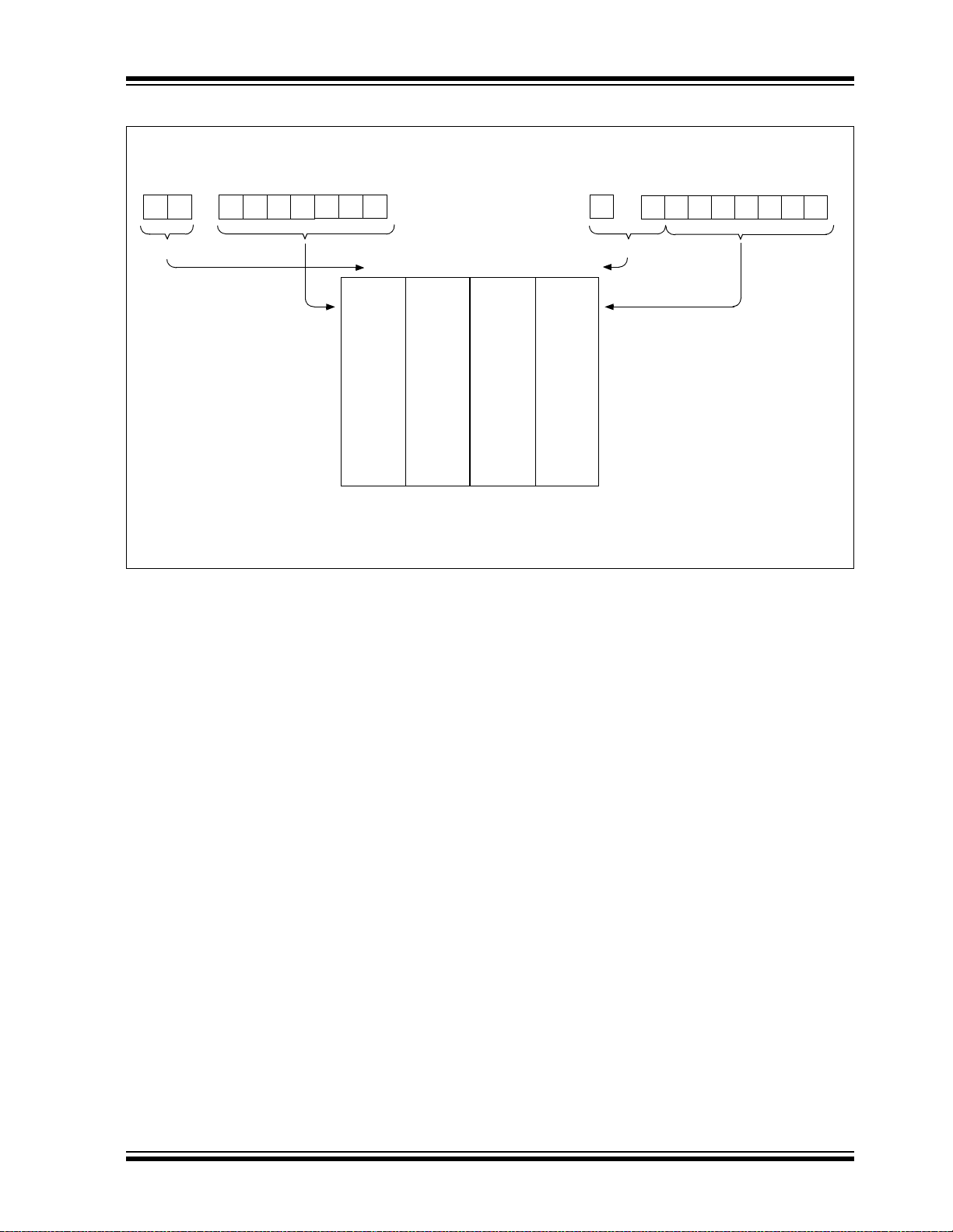
FIGURE 4-5: DIRECT/INDIRECT ADDRESSING PIC16F627A/628A/648A
Status
Register
RP1 RP0 6
bank select location select
Note: For memory map detail see Figure 4-3, Figure 4-2 and Figure 4-1.
from opcode
RAM
File
Registers
0
00 01 10 11
00h
7Fh
Bank 0 Bank 1 Bank 2 Bank 3
Status
Register
IRP FSR Register
bank select
180h
Indirect AddressingDirect Addressing
7
location select
1FFh
0
© 2007 Microchip Technology Inc. DS40044F-page 29

PIC16F627A/628A/648A
NOTES:
DS40044F-page 30 © 2007 Microchip Technology Inc.

PIC16F627A/628A/648A
n
5.0 I/O PORTS
The PIC16F627A/628A/648A have two ports, PORTA
and PORTB. Some pins for these I/O ports are
multiplexed with alternate functions for the peripheral
features on the device. In general, when a peripheral i s
enabled, that pin may not be used as a general
purpose I/ O pin.
5.1 PORTA and TRISA Registers
PORTA is an 8-bit wide latch. RA4 is a Schmitt Trigger
input and an open drain output. Port R A4 is multi plexed
with the T0CKI clock input. RA5
input only and has no output drivers. All other RA port
pins have Schmitt Trigger input levels and full CMOS
output drivers. All pins have data direction bits (TRIS
registers) which can configure these pins as input or
output.
A ‘1’ in the TRISA register puts the corresponding
output driver in a High-impedance mode. A ‘0’ in the
TRISA register puts the contents of the output latch on
the selected pin(s).
Reading the PORTA register reads the status of the
pins whereas writing to it will write to the port latch. All
write operations are re ad-modify-write operations. So a
write to a port implies that the port pins are first read,
then this value is modified and written to the port data
latch.
The PORTA pins are multiplexed with comparator and
voltage reference functions. The operation of these
pins are selected by control bits in the CMCON
(Comparator Control register) re gister a nd the VRCON
(Voltage Reference Control register) register. When
selected as a comparator input, these pins will read
as ‘0’s.
Note 1: RA5 shares function with VPP. When VPP
voltage levels are applied to RA5, the
device will enter Progra mming mode.
2: On Reset, the TRISA register is set to all
inputs. The digital inputs (RA<3:0>) are
disabled and the comparator inputs are
forced to ground to reduce current
consumption.
3: TRISA<6:7> is overridden by oscillator
configuration. When PORTA<6:7> is
overridden, the data reads ‘0’ and the
TRISA<6: 7> bits are ignored.
TRISA controls the direction of the RA pins, even when
they are being used as comparator inputs. The user
must make sure to keep the pins configured as inputs
when using them as comparator inputs.
The RA2 pin will also function as the output for the
voltage referen ce. When in this mo de, the V
very high-impedance output. The user must configure
TRISA<2> bit as an input and use high-impedance
loads.
(1)
is a Schmitt Trigger
REF pin is a
In one of the comparator modes defined by the
CMCON register, pins RA3 and RA4 become outputs
of the comparators. The TRISA<4:3> bits must be
cleared to enable outputs to use this function.
EXAMPLE 5-1: INITIALIZING PORTA
CLRF PORTA ;Initialize PORTA by
MOVLW 0x07 ;Turn comparators off and
MOVWF CMCON ;enable pins for I/O
BCF STATUS, RP1
BSF STATUS, RP0 ;Select Bank1
MOVLW 0x1F ;Value used to initialize
MOVWF TRISA ;Set RA<4:0> as inputs
;setting
;output data latches
;functions
;data direction
;TRISA<5> always
;read as ‘1’.
;TRISA<7:6>
;depend on oscillator
;mode
FIGURE 5-1: BLOCK DIAGRAM OF
RA0/AN0:RA1/AN1 PINS
Data
Bus
WR
PORTA
Data Latch
WR
TRISA
TRIS Latch
RD
TRISA
RD PORTA
To Comparator
CK
CK
QD
Q
QD
Q
Input Mode
(CMCON Reg.)
Analog
Schmitt Trigger
Input Buffer
EN
VDD
I/O Pi
VSS
DQ
© 2007 Microchip Technology Inc. DS40044F-page 31

PIC16F627A/628A/648A
in
FIGURE 5-2: BLOCK DIAGRAM OF
Data
Bus
WR
PORTA
WR
TRISA
RD
TRISA
RD PORTA
CK
Data Latch
CK
TRIS Latch
RA2/AN2/V
QD
Q
QD
Q
Input Mode
(CMCON Reg.)
Schmitt Trigger
Analog
Input Buffer
REF PIN
VDD
RA2 P
VSS
DQ
EN
To Comparator
VROE
V
REF
FIGURE 5-3: BLOCK DIAGRAM OF THE RA3/AN3/CMP1 PIN
Data
Bus
WR
PORTA
WR
TRISA
RD
TRISA
CK
Data Latch
CK
TRIS Latch
QD
Comparator Mode = 110
Comparator Output
Q
QD
Q
(CMCON Reg.)
1
0
Analog
Input Mode
(CMCON Reg.)
Schmitt Trigger
Input Buffer
DQ
EN
VDD
RA3 Pin
VSS
RD PORTA
To Comparator
DS40044F-page 32 © 2007 Microchip Technology Inc.

PIC16F627A/628A/648A
.
r
FIGURE 5-4: BLOCK DIAGRAM OF RA4/T0CKI/CMP2 PIN
Data
Bus
WR
PORTA
WR
TRISA
RD PORTA
CK
Data Latch
CK
TRIS Latch
RD TRISA
QD
Q
QD
Q
Comparator Mode = 110
Comparator Output
(CMCON Reg.)
1
0
Schmitt Trigger
Input Buffer
DQ
EN
N
Vss
RA4 Pin
Vss
TMR0 Clock Input
FIGURE 5-5: BLOCK DIAGRAM OF THE
MCLR
circuit
Program
mode
Data
Bus
RD
TRISA
RD
PORTA
MCLRE
MCLR
HV Detect
RA5/MCLR
(Configuration Bit)
Filter
Schmitt Trigger
Input Buffer
VSS
Q
D
EN
/VPP PIN
RA5/MCLR/VPP
VSS
FIGURE 5-6: BLOCK DIAGRAM OF
RA6/OSC2/CLKOUT PIN
From OSC1
CLKOUT(FOSC/4)
DCKQ
Data Latch
(2)
DCKQ
TRIS Latch
(1)
WR
PORTA
FOSC =
101, 111
WR
TRISA
RD
TRISA
OSC =
F
011, 100, 110
RD PORTA
1
0
Q
Q
QD
EN
OSC
Circuit
VDD
VSS
Schmitt
Trigger
Input Buffe
© 2007 Microchip Technology Inc. DS40044F-page 33
Note 1: INTOSC with RA6 = I/O or RC with RA6 = I/O
2: INTOSC with RA6 = CLKOUT or RC with
RA6 = CLKOUT.

PIC16F627A/628A/648A
FIGURE 5-7: BLOCK DIAGRAM OF RA7/OSC1/CLKIN PIN
Data Bus
WR PORTA
WR TRISA
RD TRISA
F
OSC = 100, 101
RD PORTA
To Clock Circuits
QD
CK
Data Latch
D
CK
TRIS Latch
Q
Q
Q
(1)
EN
VDD
RA7/OSC1/CLKIN Pin
VSS
DQ
Schmitt Trigger
Input Buffer
Note 1: INTOSC with CLKOUT and INTOSC with I/O.
DS40044F-page 34 © 2007 Microchip Technology Inc.

PIC16F627A/628A/648A
TABLE 5-1: PORTA FUNCTIONS
Name Function
Input
Type
RA0/AN0 RA0 ST CMOS Bidirectional I/O port
AN0 AN — Analog comparator input
RA1/AN1 RA1 ST CMOS Bidirectional I/O port
AN1 AN — Analog comparator input
RA2/AN2/V
REF RA2 ST CMOS Bidirectional I/O port
AN2 AN — Analog comparator input
VREF —ANVREF output
RA3/AN3/CMP1 RA3 ST CMOS Bidirectional I/O port
AN3 AN — Analog comparator input
CMP1 — CMOS Comparator 1 output
RA4/T0CKI/CMP2 RA4 ST OD Bidirectional I/O port. Output is open drain type.
T0CKI ST — External clock input for TMR0 or comparator output
CMP2 — OD Comparator 2 output
RA5/MCLR
/VPP RA5 ST — Input port
MCLR
V
PP HV —
ST — Master clear. When configured as MCLR, this pin is an
RA6/OSC2/CLKOUT RA6 ST CMOS Bidirectional I/O port
OSC2 — XTAL Oscillator crystal output. Connects to crystal resonator in
CLKOUT — CMOS In RC or INTOSC mode. OSC2 pin can output CLKOUT,
RA7/OSC1/CLKIN RA7 ST CMOS Bidirectional I/O port
OSC1 XTAL — Oscillator crystal input. Connects to crystal resonator in
CLKIN ST — External clock source input. RC biasing pin.
Legend: O = Output CMOS = CMOS Output P = Power
— = Not used I = Input ST = Schmitt Trigger Input
TTL = TTL Input OD = Open Drain Output AN = Analog
Output
Type
Description
active low Reset to the device. Volt age on MCLR
not exceed V
DD during normal device operation.
Programming voltage input
Crystal Oscillator mode.
which has 1/4 the frequency of OSC1.
Crystal Oscillator mode.
/VPP must
TABLE 5-2: SUMMARY OF REGISTERS ASSOCIATED WITH PORTA
Address Name Bit 7 B it 6 Bit 5 Bit 4 Bit 3 Bit 2 Bit 1 Bit 0
(1)
05h PORTA RA7 RA6
85h TRISA TRISA7 TRISA6 TRISA5 TRISA4 TRISA3 TRISA2 TRISA1 TRISA0 1111 1111 1111 1111
1Fh CMCON
9Fh VRCON VREN VROE
Legend: - = Unimplemented locations read as ‘0’, u = unchanged, x = unknown, q = value depends on condition. Shaded cells
are not used for PORTA.
Note 1: MCLRE configuration bit sets RA5 functionality.
© 2007 Microchip Technology Inc. DS40044F-page 35
C2OUT C1OUT C2INV C1INV CIS CM2 CM1 CM0 0000 0000 0000 0000
RA5
VRR — VR3 VR2 VR1 VR0 000- 0000 000- 0000
RA4 RA3 RA2 RA1 RA0 xxxx 0000 qqqu 0000
Value on
POR
Value on
All Other
Resets

PIC16F627A/628A/648A
T
p
5.2 PORTB and TRISB Registers
PORTB is an 8-bit wide bidirectional port. The
corresponding data direction register is TRISB. A ‘1’ in
the TRISB register put s the correspondi ng output driver
in a High-impedance mode. A ‘0’ in the TRISB register
puts the conten ts of the output latch on the se lected
pin(s).
PORTB is multiplexed with the external interrupt,
USART, CC P module and the TMR1 clock inpu t/output.
The standard port functions and the alternate port
functions are shown in Table 5-3. Alternate port
functions may overri de the TRIS sett ing when ena bled.
Reading PORTB register reads the status of the pins,
whereas writing to it will write to the port latch. All write
operations are read- modify-write op erations. So a wri te
to a port implies that the port pins are first read, then
this value is modified and written to the port da t a l atc h.
Each of the PORTB pins has a weak internal pull-up
(≈200 μA t ypical). A si ngle con trol bit ca n turn on al l the
pull-ups. This is done by clearing the RBPU
(OPTION<7>) bit. The weak pull-up is automatically
turned off when the port pin is configured as an output.
The pull-ups are disabled on Power-on Reset.
Four of PORTB’s pins, RB<7:4>, have an interrupt-onchange feature. Only pins configured as inputs can
cause this interrupt to occur (i.e., any RB<7:4> pin
configured as an output is excluded from the interrupton-change comparison). The input pins (of RB<7:4>)
are compared with the old value latched on the last
read of PORTB. The “mismatch” outputs of RB<7:4>
are OR’ed together to genera te the R BIF inte rrupt (fla g
latched in INTCON<0>).
This interrupt can wake the device from Sleep. The
user, in the interrupt service routine, can clear the
interrupt in the following manne r :
a) Any read or write of PORTB. This will end the
mismatch condition.
b) Clear flag bit RBIF.
A mismatch condition will continue to set flag bit RBIF.
Reading PORTB will end the mismatch condition and
allow flag bit RBIF to be cleared.
This interrupt on mismatch feature, together with
software configurable pull-ups on these four pins allow
easy interface to a key pad and make it possible for
wake-up on key-depression (See Application Note
AN552 “Implementing Wake-up on Key Strokes”
(DS00552).
Note: If a change on the I/O pin should occur
when a read operation is being executed
(start of the Q2 cycle), then the RBIF
interrupt flag may not get set.
The interrupt-on-change feature is recommended for
wake-up on key depression operation and operations
where PORTB is only used for the interrupt-on-change
feature. Polling of PORTB is not recommended while
using the interrupt-on-change feature.
FIGURE 5-8: BLOCK DIAGRAM OF
RB0/INT PIN
TTL
Input
Buffer
VDD
Weak Pull-u
P
VDD
RB0/IN
VSS
RBPU
Data Bus
WR PORTB
WR TRISB
RD TRISB
RD PORTB
INT
D
Q
CK
Q
Data Latch
D
Q
Q
CK
TRIS Latch
Schmitt
Trigger
QD
EN
EN
DS40044F-page 36 © 2007 Microchip Technology Inc.

PIC16F627A/628A/648A
FIGURE 5-9: BLOCK DIAGRAM OF
RB1/RX/DT PIN
VDD
RBPU
SPEN
USART Data Output
Data Bus
WR PORTB
WR TRISB
Peripheral OE
RD TRISB
RD PORTB
(1)
D
Q
CK
Q
Data Latch
D
CK
Q
TRIS Latch
1
0
Q
QD
EN
TTL
Input
Buffer
P
Weak
Pull-up
VDD
VSS
RB1/
RX/DT
FIGURE 5-10: BLOCK DIAGRAM OF
RB2/TX/CK PIN
TTL
Input
Buffer
VDD
P
Weak
Pull-up
VDD
VSS
RBPU
SPEN
USART TX/CK Output
Data Bus
WR PORTB
WR TRISB
Peripheral OE
RD TRISB
RD PORTB
(1)
D
Q
CK
Q
Data Latch
D
CK
Q
TRIS Latch
1
0
Q
QD
EN
RB2/
TX/CK
USART Receive Input
Schmitt
Trigger
Note 1: Peripheral OE (output enable) is only active if
peripheral select is active.
USART Slave Clock In
Schmitt
Trigger
Note 1: Peripheral OE (output enable) is only active if
peripheral select is active.
© 2007 Microchip Technology Inc. DS40044F-page 37

PIC16F627A/628A/648A
FIGURE 5-11: BLOCK DIAGRAM OF
RB3/CCP1 PIN
RBPU
CCP1CON
VDD
P
Weak
Pull-up
VDD
CCP output
Data Bus
WR PORTB
WR TRISB
Peripheral OE
RD TRISB
RD PORTB
CCP In
Note 1: Peripheral OE (output enable) is only active if
D
Q
CK
Q
Data Latch
D
Q
CK
Q
TRIS Latch
(2)
Schmitt
Trigger
peripheral select is active.
0
1
QD
EN
TTL
Input
Buffer
VSS
RB3/
CCP1
DS40044F-page 38 © 2007 Microchip Technology Inc.
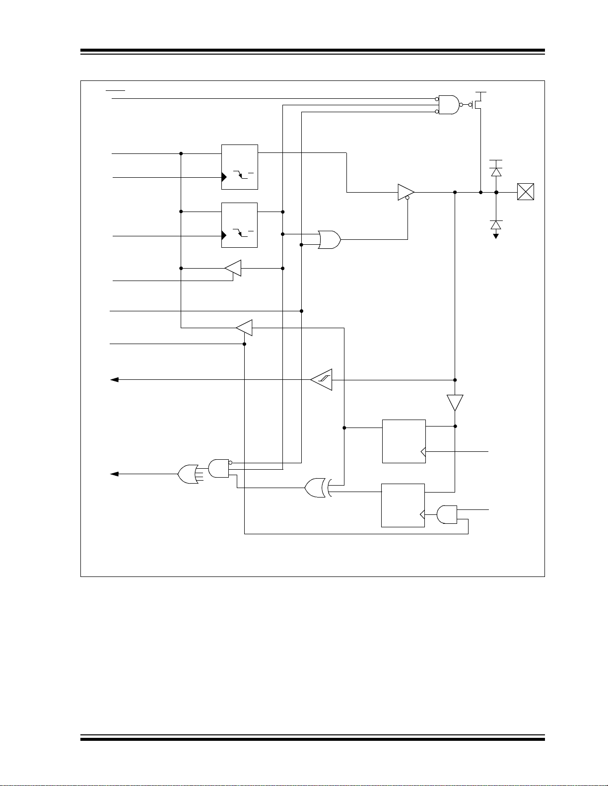
PIC16F627A/628A/648A
FIGURE 5-12: BLOCK DIAGRAM OF RB4/PGM PIN
RBPU
VDD
P
weak pull-up
Data Bus
WR PORTB
WR TRISB
RD TRISB
(Configuration Bit)
LVP
RD PORTB
PGM input
D
CK
Data Latch
D
CK
TRIS Latch
Q
Q
Q
Q
Schmitt
Trigger
QD
TTL
input
buffer
VDD
RB4/PGM
VSS
EN
Set RBIF
From other
RB<7:4> pins
QD
EN
Note: The low-voltage programming disables the interrupt-on-change and the weak pull-ups on RB4.
Q1
Q3
© 2007 Microchip Technology Inc. DS40044F-page 39

PIC16F627A/628A/648A
FIGURE 5-13: BLOCK DIAGRAM OF RB5 PIN
RBPU
V
DD
P
weak
pull-up
VDD
Data Bus
WR PORTB
WR TRISB
RD TRISB
RD PORTB
Set RBIF
D
Q
Q
CK
Data Latch
D
Q
CK
Q
TRIS Latch
From other
RB<7:4> pins
QD
EN
QD
EN
TTL
input
buffer
RB5 pin
VSS
Q1
Q3
DS40044F-page 40 © 2007 Microchip Technology Inc.

PIC16F627A/628A/648A
/
FIGURE 5-14: BLOCK DIAGRAM OF RB6/T1OSO/T1CKI/PGC PIN
RBPU
Data Bus
WR PORTB
WR TRISB
RD TRISB
T1OSCEN
RD PORTB
TMR1 Clock
From RB7
Serial Programming Clock
D
CK
Data Latch
D
CK
TRIS Latch
VDD
P
weak pull-up
Q
Q
Q
Q
Schmitt
Trigger
TMR1 oscillator
TTL
input
buffer
VDD
VSS
RB6/
T1OSO
T1CKI/
PGC
pin
QD
Q1
Q3
Set RBIF
From other
RB<7:4> pins
EN
QD
EN
© 2007 Microchip Technology Inc. DS40044F-page 41

PIC16F627A/628A/648A
I/
FIGURE 5-15: BLOCK DIAGRAM OF THE RB7/T1OSI/PGD PIN
RBPU
VDD
weak pull-up
P
To RB6
Data Bus
WR PORTB
WR TRISB
RD TRISB
T10SCEN
RD PORTB
Serial Programming Input
D
CK
Data Latch
D
CK
TRIS Latch
TMR1 oscillator
VDD
Q
Q
Q
Q
Schmitt
Trigger
QD
RB7/T1OS
PGD pin
VSS
TTL
input
buffer
Set RBIF
From other
RB<7:4> pins
EN
QD
EN
Q1
Q3
DS40044F-page 42 © 2007 Microchip Technology Inc.

PIC16F627A/628A/648A
TABLE 5-3: PORTB FUNCTIONS
Name Function Input Type
RB0/INT RB0 TTL CMOS Bidirectional I/O port. Can be software programmed for
INT ST — External interrupt
RB1/RX/DT RB1 TTL CMOS Bidirectional I/O port. Can be software programmed for
RX ST — USART Receive Pin
DT ST CMOS Synchronous data I/O
RB2/TX/CK RB2 TTL CMOS Bidirectional I/O port
TX — CMOS USART Transmit Pin
CK ST CMOS Synchronous Clock I/O. Can be software programmed
RB3/CCP1 RB3 TTL CMOS Bidirectional I/O port. Can be software programmed for
CCP1 ST CMOS Capture/Compare/PWM/I/O
RB4/PGM RB4 TTL CMOS Bidirectional I/O port. Interrupt-on-pin change. Can be
PGM ST — Low-voltage programming input pin. When low-voltage
RB5 RB5 TTL CMOS Bidirectional I/O port. Interrupt-on-pin change. Can be
RB6/T1OSO/T1CKI/
RB6 TTL CMOS Bidirectional I/O port. Interrupt-on-pin change. Can be
PGC
T1OSO — XTAL Timer1 Oscillator Output
T1CKI ST — Timer1 Clock Input
PGC ST — ICSP
RB7/T1OSI/PGD RB7 TTL CMOS Bidirectional I/O port. Interrupt-on-pin change. Can be
T1OSI XTAL — Timer1 Oscillator Input
PGD ST CM OS ICSP Data I/O
Legend: O = Output CMOS = CMOS Output P = Power
— = Not used I = Input ST = Schmitt Trigger Input
TTL = TTL Input OD = Open Drain Output AN = Analog
Output
Type
Description
internal weak pull-up.
internal weak pull-up.
for internal weak pull-up.
internal weak pull-up.
software programmed for internal weak pull-up.
programming is enabled, the interrup t-on-pin change
and weak pull-up resistor are disabled.
software programmed for internal weak pull-up.
software programmed for internal weak pull-up.
™
Programming Clock
software programmed for internal weak pull-up.
TABLE 5-4: SUMMARY OF REGISTERS ASSOCIATED WITH PORTB
Address Name Bit 7 Bit 6 Bit 5 Bit 4 Bit 3 Bit 2 Bit 1 Bit 0
(1)
06h, 106h PORTB RB7 RB6 RB5 RB4
86h, 186h TRISB TRISB7 TRISB6 TRISB5 TRISB4 TRISB3 TRISB2 TRISB1 TRISB0 1111 1111 1111 1111
81h, 181h OPTION RBPU
Legend: u = unchanged, x = unknown. Shaded cells are not used for PORTB.
Note 1: LVP configuration bit sets RB4 functionality.
© 2007 Microchip Technology Inc. DS40044F-page 43
INTEDG T0CS T0SE PSA PS2 PS1 PS0 1111 1111 1111 1111
RB3 RB2 RB1 RB0 xxxx xxxx uuuu uuuu
Value on
POR
Value on
All Other
Resets
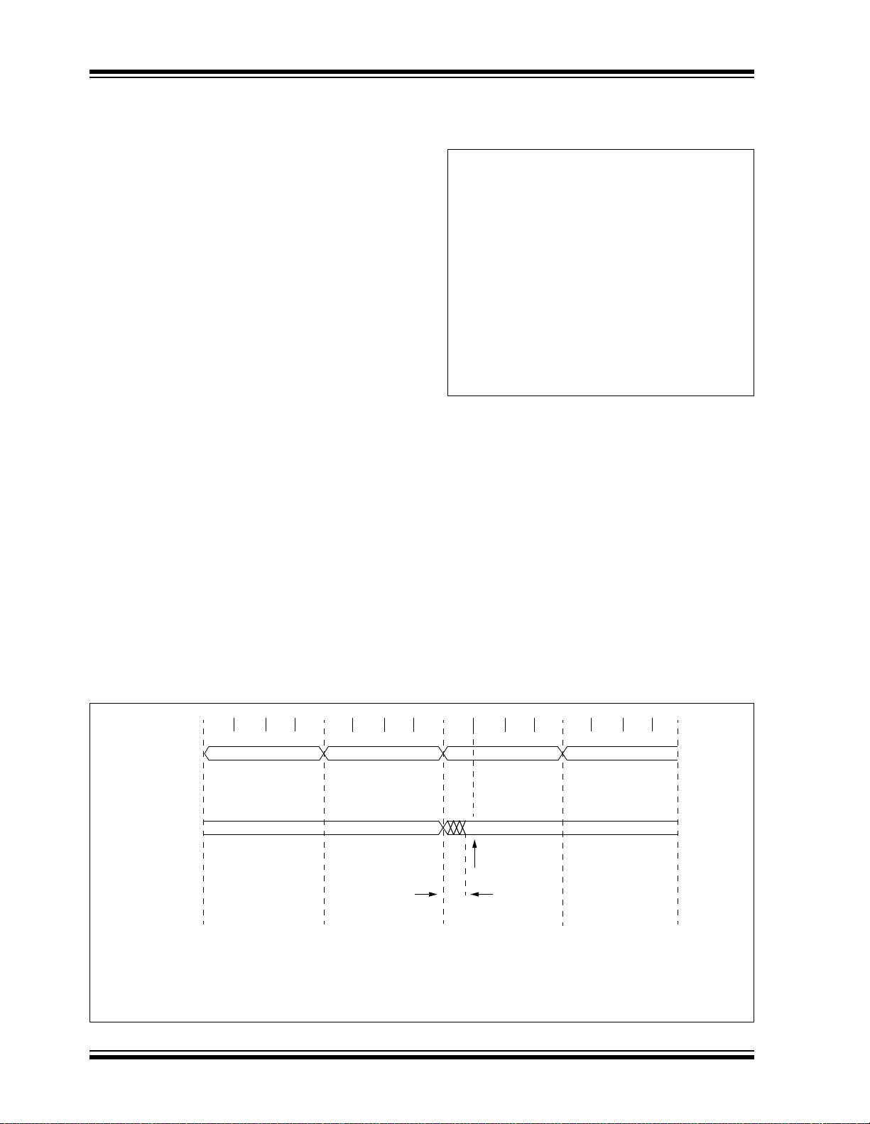
PIC16F627A/628A/648A
5.3 I/O Programming Considerations
5.3.1 BIDIREC TION AL I/O PORTS
Any instruction that write s operates int ernally as a read
followed by a write operation. The BCF and BSF
instructions, for example, read the register into the
CPU, execute the bit operation and write the result
back to the register. Caution must be used when t hes e
instructions are applied to a port with both inputs and
outputs defined. Fo r ex am ple , a BSF operation on bit 5
of PORTB will caus e all ei ght bit s of POR TB to b e read
into the CPU. Then the BSF operation takes place on
bit 5 and PORTB is written to the output latches. If
another bit of PORTB is used as a bidirectional I/O pin
(e.g., bit 0) and is defined as an input at this time, the
input signal presen t on th e pi n it s el f wo uld be rea d in to
the CPU and rewritten to the dat a latch of this p articular
pin, overwriting the previous co ntent. As long as the pin
stays in the Input mode, no problem occurs. However,
if bit 0 is switched into Output mode later on, the
content of the data latch may now be unknown.
Reading a port register reads the values of the port
pins. Writing to the port register writes the value to the
port latch. When using read-modify-write instructions
(ex. BCF, BSF, etc.) on a port, the v alue of the po rt pin s
is read, the desired o pera tion is done to this value , and
this value is then written to the port latch.
Example 5-2 shows the effect of two sequential readmodify-write instructions (ex., BCF, BSF, etc.) on an
I/O port.
A pin actively outputting a Low or High should not be
driven from external devices at the same time in order
to change the level on this pin (“wired-OR”, “wiredAND”). The resulting high out put current s may damag e
the chip.
EXAMPLE 5-2: READ-MODIFY-WRITE
INSTRUCTIONS ON AN
I/O PORT
;Initial PORT settings:PORTB<7:4> Inputs
; PORTB<3:0> Outputs
;PORTB<7:6> have external pull-up and are
;not connected to other circuitry
;
; PORT latchPORT Pins
---------- ---------BCF STATUS, RP0 ;
BCF PORTB, 7 ;01pp pppp 11pp pppp
BSF STATUS, RP0 ;
BCF TRISB, 7 ;10pp pppp 11pp pppp
BCF TRISB, 6 ;10pp pppp 10pp pppp
;
;Note that the user may have expected the
;pin values to be 00pp pppp. The 2nd BCF
;caused RB7 to be latched as the pin value
;(High).
5.3.2 SUCCESSIVE OPERATIONS ON I/O PORTS
The actual wri te to an I/ O port hap pens at t he end of
an instruction cycle, whereas for reading, the data
must be valid at the be ginni ng o f t he i nstru ction cycl e
(Figure 5-16). T herefore, ca re must be e xercised if a
write followed by a read operation is carried out on the
same I/O port. The sequence of instructions should be
such to allow the pin voltage to stabilize (load
dependent) befo re th e next i nstruct ion, whi ch ca uses
that file to be read into the CPU, is ex ecuted. Ot herwise, the previous state of that pin may be read into
the CPU rather t han the new state. W hen in do ubt, it
is better to separate these inst ructions with a NOP or
another instructio n no t acc essi ng this I/O po rt.
FIGURE 5-16: SUCCESSIVE I/O OPERATION
Q1 Q2 Q3 Q4
PC
Instruction
fetched
Note 1: This example shows write to PORTB followed by a read from PORTB.
2: Data setup time = (0.25 T
to output valid. Therefore, at higher clock frequencies, a write followed by a read may be problematic.
DS40044F-page 44 © 2007 Microchip Technology Inc.
PC
MOVWF PORTB
Write to PORTB
Q1 Q2 Q3 Q4 Q1 Q2 Q3 Q4 Q1 Q2 Q3 Q4
PC + 1
MOVF PORTB, W
Read to PORTB
TPD
Execute
MOVWF
PORTB
CY - TPD) where TCY = in structi on cycl e and TPD = p ropaga tion de lay of Q1 cycle
PC + 2 PC + 3
NOP NOP
Port pin
sampled here
Execute
MOVF
PORTB, W
Execute
NOP

PIC16F627A/628A/648A
6.0 TIMER0 MODULE
The Timer0 module timer/counter has the following
features:
• 8-bit timer/counter
• Read/write capabilities
• 8-bit software programmable prescaler
• Internal or external clock select
• Interrupt on overflow from FFh to 00h
• Edge select for external clock
Figure 6-1 is a simplified block diagram of the Timer0
module. Additional information is available in the “PIC
Mid-Range MCU Family Reference Manual” (DS3302 3).
Timer mode is selected by clearing the T0CS bit
(OPTION<5>). In T imer mode, the TMR0 register value
will increment every instruction cycle (without
prescaler). If the TMR0 register is written to, the
increment is inhibited for the following two cycles. The
user can work around this by writing an adjusted value
to the TMR0 register.
Counter mode is selected by setting the T0CS bit. In
this mode the TMR0 register value will incremen t either
on every rising or fal ling edge of p in RA4/T0CKI/C MP2.
The incrementing edge is determined by the source
edge (T0SE) control bit (OPTION<4>). Clearing the
T0SE bit selects the rising edge. Restrictions on the
external clock input are discussed in detail in
Section 6.2 “Using Timer0 with External Clock”.
The prescaler is shared between the Timer0 module
and the Watchdog Timer. The prescaler assignment is
controlled in software by the control bit PSA
(OPTION<3>). Clearing the PSA bit will assign the
prescaler to Timer0. The prescaler is not readable or
writable. When the pr es cal er is ass ign ed to th e Timer0
module, prescale value of 1:2, 1:4,..., 1:256 are
selectable. Section 6.3 “Timer0 Prescaler” details
the operation of the prescaler.
6.2 Using Timer0 with External Clock
When an external clock input i s used for T ime r0, it must
meet certain requirements. The external clock
requirement is due to internal phase clock (T
synchronization. Also, there is a delay in the actual
incrementing of Timer0 after synchronization.
6.2.1 EXTERNAL CLOCK SYNCHRONIZATION
When no prescaler is used, the external clock input is
the same as the prescaler outp ut. The synch ronization
®
of T0CKI with the internal phase clocks is
accomplished by sampling the prescaler output on the
Q2 and Q4 cycles of the internal phase clocks
(Figure 6-1). Therefore, it is necessary for T0CKI to be
high for at least 2T
and low for at least 2T
20 ns). Refer to the electrical specification of the
desired device.
When a prescaler is used, the external clock input is
divided by the asynchronous ripple-counter type
prescaler so that the prescaler output is symmetrical.
For the external clock to meet the sampling
requirement, the ripple-counter must be taken into
account. Therefore, it is necessary for T0CK I to have a
period of at least 4T
divided by the prescaler value. The only requirement
on T0CKI hig h and lo w time is that th ey do no t violat e
the minimum pulse w idth require ment of 10 ns. Refer to
parameters 40 , 41 a nd 42 in the electrical specification
of the desired device. See Table17-8.
OSC (and a small RC d elay of 20 ns)
OSC (and a small RC delay of
OSC (and a small RC delay of 40 ns)
OSC)
6.1 Timer0 Interrupt
Timer0 interrupt is generated when the TMR0 register
timer/counter overflows from FFh to 00 h. This overfl ow
sets the T0IF bit. The interrupt can be masked by
clearing the T0IE bit (INTCON<5>). The T0IF bit
(INTCON<2>) must be cleared in software by the
Timer0 module interrupt service routine before reenabling this interrupt. The Timer0 interrupt cannot
wake the processor from Sleep since the timer is shut
off during Sleep.
© 2007 Microchip Technology Inc. DS40044F-page 45

PIC16F627A/628A/648A
6.3 Timer0 Prescaler
An 8-bit counter is available as a prescaler for the
Timer0 module, or as a postscaler for the Watchdog
Timer. A prescaler assignment for the Timer0 module
means that there is no postscaler for the Watchdog
Timer, and vice-versa.
The PSA and PS<2:0> bits (OPTION<3:0>) determine
the prescaler assignment and prescale ratio.
When assigned to the Timer0 module, all instructions
writing to the TMR0 register (e.g., CLRF 1, MOVWF 1,
BSF 1, x....etc.) will clear the prescaler. When
assigned to WDT, a CLRWDT instruction will clear the
prescaler along with the Wa tchdog Timer . The pres caler
is not readable or writable.
FIGURE 6-1: BLOCK DIAGRAM OF THE TIMER0/WDT
F
OSC/4
0
T0CKI
pin
Watchdog
Timer
T0SE
1
T0CS
TMR1 Clock Source
0
1
PSA
WDT Postscaler/
TMR0 Prescaler
8
8-to-1MUX
1
0
PSA
SYNC
2
Cycles
PS<2:0>
Data Bus
8
TMR0 Reg
Set flag bit T0IF
on Overflow
WDT Enable bit
PSA
Note: T0SE, T0CS, PSA, PS<2:0> are bits in the Option Register.
.
1
0
WDT
Time-out
DS40044F-page 46 © 2007 Microchip Technology Inc.

PIC16F627A/628A/648A
6.3.1 SWITCHING PRESCALER ASSIGNMENT
The prescaler assignment is fully under software
control (i.e., it can be changed “on-the-fly” during
program execution). Use the instruction sequences
shown in Example 6-1 when changing the prescaler
assignment from Timer0 to WDT, to avoid an
unintended device Reset.
EXAMPLE 6-1: CHANGING PRESCALER
(TIMER0 → WDT)
BCF STATUS, RP0 ;Skip if already in
;Bank 0
CLRWDT ;Clear WDT
CLRF TMR0 ;Clear TMR0 and
;Prescaler
BSF STATUS, RP0 ;Bank 1
MOVLW '00101111’b ;These 3 lines
;(5, 6, 7)
MOVWF OPTION_REG ;are required only
;if desired PS<2:0>
;are
CLRWDT ;000 or 001
MOVLW '00101xxx’b ;Set Postscaler to
MOVWF OPTION_REG ;desired WDT rate
BCF STATUS, RP0 ;Return to Bank 0
To change prescaler from the WDT to the Timer0
module, use the se quence sh own in Examp le 6-2. This
precaution must be t aken even if the WDT is disabled.
EXAMPLE 6-2: CHANGIN G PRESCALER
(WDT → TIMER0)
CLRWDT ;Clear WDT and
;prescaler
BSF STATUS, RP0
MOVLW b'xxxx0xxx’ ;Select TMR0, new
;prescale value and
;clock source
MOVWF OPTION_REG
BCF STATUS, RP0
TABLE 6-1: REGISTERS ASSOCIATED WITH TIMER0
Address Name Bit 7 Bit 6 Bit 5 Bit 4 Bit 3 Bit 2 Bit 1 Bit 0
01h, 101h TMR0 Timer0 Module Register xxxx xxxx uuuu uuuu
0Bh, 8Bh,
10Bh, 18Bh
81h, 181h
85h TRISA
Legend: - = Unimplemented locations, read as ‘0’, u = unchanged, x = unknown. Shaded cells are not used for Timer0.
Note 1: Option is referred by OPTION_REG in MPLAB
INTCON GIE
(2)
OPTION
RBPU INTEDG T0CS T0SE PSA PS2 PS1 PS0 1111 1111 1111 1111
TRISA7 TRISA6 TRISA5 TRISA4 TRISA3 TRISA2 TRISA1 TRISA0 1111 1111 1111 1111
PEIE T0IE INTE RBIE T0IF INTF RBIF 0000 000x 0000 000u
®
IDE Software.
Value on
POR
Val ue on
All Other
Resets
© 2007 Microchip Technology Inc. DS40044F-page 47

PIC16F627A/628A/648A
7.0 TIMER1 MODULE
The Timer1 mod ule is a 16-bi t timer/c ou nter c ons isting
of two 8-bit registers (TMR1H and TMR1L) which are
readable and writable. The TMR1 register pair
(TMR1H:TMR1L) increments from 0000h to FFFFh
and rolls over to 0000h. The Timer1 Interrupt, if
enabled, is generated on overflow of the TMR1 reg ister
pair which latches the interrupt flag bit TMR1IF
(PIR1<0>). This interrupt can be enabled/disabled by
setting/clearing the T i mer1 interru pt enable bi t TMR1IE
(PIE1<0>).
Timer1 can operate in one of two modes:
•As a timer
•As a counter
The Operating mode is determined by the clock select
bit, TMR1CS (T1CON<1>).
In Timer mode, the TMR1 register pair value
increments every instruction cycle. In Counter mode, it
increments on every rising edge of the external clock
input.
Timer1 can be enabled/disabled by setting/clearing
control bit TMR1ON (T1CON<0> ) .
Timer1 also has an interna l “Reset in put”. This Reset
can be generated by the CCP module (Section 9.0
“Capture/Compare/PWM (CCP) Module”).
Register 7-1 shows the Timer1 control register.
For the PIC16F627A/628A/648A, when the Timer1
oscillator is enabled (T1OSCEN is set), the RB7/
T1OSI/PGD and RB6/T1OSO/T1CKI/PGC pins
become inputs. That is, the TRISB<7:6> value is
ignored.
REGISTER 7-1: T1CON – TIMER1 CONTROL REGISTER (ADDRESS: 10h)
U-0 U-0 R/W-0 R/W-0 R/W-0 R/W-0 R/W-0 R/W-0
— — T1CKPS1 T1CKPS0 T1OSCEN T1SYNC TMR1CS TMR1ON
bit 7 bit 0
bit 7-6 Unimplemented: Read as ‘0’
bit 5-4 T1CKPS<1:0>: Timer1 Input Clock Prescale Select bits
11 = 1:8 Prescale value
10 = 1:4 Prescale value
01 = 1:2 Prescale value
00 = 1:1 Prescale value
bit 3 T1OSCEN: Timer1 Oscillator Enable Contr ol bit
1 = Oscillator is enabled
0 = Oscillator is shut off
bit 2 T1SYNC: Timer1 External Clock Input Synchronization Control bit
TMR1CS = 1
1 = Do not synchronize external clock input
0 = Synchronize external clock input
TMR1CS = 0
This bit is ignored. Timer1 uses the internal clock when TMR1CS = 0.
bit 1 TMR1CS: Timer1 Clock Source Select bit
1 = External clock from pin RB6/T1OSO/T1CKI/PGC (on the rising edge)
0 = Internal clock (F
bit 0 TMR1ON: Timer1 On bit
1 = Enables Timer1
0 = Stops Timer1
Note 1: The oscillator inverter and feedback resistor ar e turned of f to eli minate p ower drain.
(1)
OSC/4)
Legend:
R = Readable bit W = Writable bit U = Unimplemented bit, read as ‘0’
-n = Value at POR ‘1’ = Bit is set ‘0’ = Bit is cleared x = Bit is unknown
DS40044F-page 48 © 2007 Microchip Technology Inc.

PIC16F627A/628A/648A
7.1 Timer1 Operation in Timer Mode
Timer mode is selected by clearing the TMR1CS
(T1CON<1>) bit. In this mode, the input clock to the
timer is F
OSC/4. The synchronize control bit T1SYNC
(T1CON<2>) has no effect since t he internal clo ck is
always in sync.
7.2 Timer1 Operation in Sync hronized Counter Mode
Counter mode is selected by setting bit TMR1CS. In
this mode, the TMR1 register pair value increments on
every rising edg e of clock inpu t on pin RB7/T1O SI/PGD
when bit T1OSCEN is set or pin RB6/T1OSO/T1CKI/
PGC when bit T1OSCEN is cleared.
If T1SYNC
synchronized with internal phase clocks. The synchronization is done after the prescaler stage. The
prescaler stage is an asynchronous ripple-counter.
In this configuration, during Sleep mode, the TMR1
register pair value will not increment even if the
external clock is present, since the synchronization
circuit is s hut off. Th e prescal er howeve r will co ntinue
to increment.
is cleared, th en the extern al clock input is
7.2.1 EXTERNAL CLOCK INPUT TIMING FOR SYNCHRONIZED COUNTER MODE
When an external clock input is used for Timer1 in
Synchronized Counter mode, it must meet certain
requirements. The external clo ck requ iremen t is due to
internal phase clock (T
there is a delay in the actual increm enting o f the TMR 1
register pair value after synchronization.
When the prescaler is 1:1, the external clock input is
the same as the prescaler outp ut. The synch ronization
of T1CKI with the internal phase clocks is accomplished by sampli ng the presc aler output on the Q2 and
Q4 cycles of the internal phase clocks. Therefore, it is
necessary for T1C KI to b e high for at leas t 2 T
a small RC delay of 20 ns) and low for at least 2 T
(and a small RC delay of 20 ns). Re fer to Table 17-8 in
the Electrical Specification s Section, timing pa rameters
45, 46 and 47.
When a prescaler other than 1:1 is used, the external
clock input is divided by the asynchronous ripple-counter
type prescaler so that the prescaler output is symmetrical. In order for the external clock to meet the sampling
requirement, the ripple-counter must be taken into
account. Therefore, it is necessary for T1CKI to have a
period of at least 4 T
divided by the prescaler value. The only requireme nt on
T1CKI high and low time is that they do not violate the
minimum pulse width requirements of 10 ns). Refer to
the appropriate electrical specifications in Table 17-8,
parameters 45, 46 and 47.
OSC) synchronization. Also,
OSC (and
OSC
OSC (and a small RC delay of 40 ns)
FIGURE 7-1: TIMER1 BLOCK DIAGRAM
Set flag bit
TMR1IF on
Overflow
RB6/T1OSO/T1CKI/PGC
RB7/T1OSI/PGD
Note 1: When the T1OSCEN bit is cleared, the inverter and feedback resistor are turned off. This eliminates power drain.
TMR1H
T1OSC
TMR1
TMR1L
T1OSCEN
Enable
Oscillator
TMR1ON
1
FOSC/4
Internal
(1)
Clock
0
TMR1CS
0
1
T1SYNC
Prescaler
1, 2, 4, 8
2
T1CKPS<1:0>
Synchronized
Clock Input
Synchronize
det
Sleep Input
© 2007 Microchip Technology Inc. DS40044F-page 49

PIC16F627A/628A/648A
7.3 Timer1 Operation in Asynchronous Counter Mode
If control bit T1SYNC (T1CON<2>) is set, the external
clock input is not synchronized. The timer continues to
increment asynchronous to the internal phase clocks.
The timer will continue to run during Sleep and can
generate an interrupt on overflow, w hich will wake-up the
processor. H owever , speci al precautions in software are
needed to read/write the timer (Section 7.3.2 “Reading
and Writing Timer1 in Asynchronous Counter
Mode”).
Note: In Asynchronous Counter mode, Timer1
cannot be used as a tim e base for ca pture
or compare operations.
7.3.1 EXTERNAL CLOCK INPUT TIMING
WITH UNSYNCHRONIZED CLOCK
If control bit T1SYNC is set, the timer will increment
completely asynch ronous ly. The in put cloc k must meet
certain minimum hig h and low time requi rements. Re fer
to Table 17-8 in the Electrical Specifications Section,
timing parameters 45, 46 and 47.
7.3.2 READING AND WRITING TIMER1 IN
ASYNCHRONOUS COUNTER
MODE
Reading the TMR1H or TMR1L reg ister , while the tim er
is running from an external asynchronous clock, will
produce a valid read (taken care of in hardware).
However, the user should keep in mind that reading the
16-bit timer in two 8-bit values itself poses certain
problems since the timer may overflow between the
reads.
For writes, it is recomm ended that the us er simply stop
the timer and write the desired values. A write
contention may occur by writing to the timer registers
while the register is incrementi ng. This may pro duce an
unpredictable value in the timer register.
Reading the 16-bit value requires some care.
Example 7-1 is an example routine to read the 16-bit
timer value. This is useful if the timer cannot be
stopped.
EXAMPLE 7-1: READING A 16-BIT FREE-
RUNNING TIMER
; All interrupts are disabled
MOVF TMR1H, W ;Read high byte
MOVWF TMPH ;
MOVF TMR1L, W ;Read low byte
MOVWF TMPL ;
MOVF TMR1H, W ;Read high byte
SUBWF TMPH, W ;Sub 1st read with
;2nd read
BTFSC STATUS,Z ;Is result = 0
GOTO CONTINUE ;Good 16-bit read
;
; TMR1L may have rolled over between the
; read of the high and low bytes. Reading
; the high and low bytes now will read a good
; value.
;
MOVF TMR1H, W ;Read high byte
MOVWF TMPH ;
MOVF TMR1L, W ;Read low byte
MOVWF TMPL ;
; Re-enable the Interrupts (if required)
CONTINUE ;Continue with your
;code
DS40044F-page 50 © 2007 Microchip Technology Inc.

PIC16F627A/628A/648A
7.4 Timer1 Oscillator
A crystal oscillator circuit is built in be tween pins T1OSI
(input) and T1OSO (amplifier output). It is enabled by
setting control bit T1OSCEN (T1CON<3>). It will
continue to run during Sleep. It i s primaril y inten ded for
a 32.768 kHz watch crystal. Table 7-1 shows the
capacitor selection for the Timer1 oscillator.
The user must provide a sof tware t im e del ay to en su re
proper oscillator start-up.
TABLE 7-1: CAPACITOR SELECTION FOR
THE TIMER1 OSCILLATOR
Freq C1 C2
32.768 kHz 15 pF 15 pF
Note: These values are for design guidance only .
Consult Application Note AN826 “Crystal
Oscillator Basics and Crystal Selection for
®
and PIC® Devices” (DS00826) for
rfPIC
further information on Crystal/Capacitor
Selection.
7.5 Resetting Timer1 Using a CCP Trigger Output
If the CCP1 module is configured in Compare mode to
generate a “special event trigger” (CCP1M<3:0> =
1011), this signal will reset Timer1.
Note: The special event triggers from the CCP1
module will not set interrupt flag bit
TMR1IF (PIR1<0>).
Timer1 must be configured for either timer or
Synchronized Counter mode to take advantage of this
feature. If Timer1 is running in Asynchronous Counter
mode, this Reset operation may not work.
In the event that a write to Timer1 coincides with a
special event trigger from CCP1, the write will take
precedence.
In this mode of operation, the CCPRxH:CCPRxL
register pair ef fe cti ve ly b ec ome s th e pe riod regi ste r for
Timer1.
7.6 Resetting Timer1 Register Pair (TMR1H, TMR1L)
TMR1H and TMR1L registers are not reset to 00h on
a POR or any other Reset except by the CCP1 special
event triggers (see Section 9.2.4 “Special Event
Trigger”).
T1CON register is rese t to 00h on a Powe r-on Rese t or
a Brown-out Reset, which shuts off the timer and
leaves a 1:1 prescale. In all other Resets, the register
is unaffected.
7.7 Timer1 Prescaler
The prescaler counter is cleared on writes to the
TMR1H or TMR1L registers.
TABLE 7-2: REGISTERS ASSOCIATED WITH TIMER1 AS A TIMER/COUNTER
Address Name Bit 7 Bit 6 Bit 5 Bit 4 Bit 3 Bit 2 Bit 1 Bit 0
0Bh, 8Bh,
10Bh, 18Bh
0Ch PIR1
8Ch PIE1
0Eh TMR1L Holding Register for the Least Significant Byte of the 16-bit TMR1 Register xxxx xxxx uuuu uuuu
0Fh TMR1H Holding Register for the Most Significant Byte of the 16-bit TMR1 Register xxxx xxxx uuuu uuuu
10h T1CON
Legend: x = unknown , u = unchanged, - = unimplemented read as ‘0’. Shaded cells are not used by the Timer1 module.
INTCON GIE PEIE
EEIF CMIF RCIF TXIF — CCP1IF TMR2IF TMR1IF 0000 -000 0000 -000
EEIE CMIE RCIE TXIE — CCP1IE TMR2IE TMR1IE 0000 -000 0000 -000
— — T1CKPS1 T1CKPS0 T1OSCEN T1SYNC TMR1CS TMR1ON --00 0000 --uu uuuu
T0IE INTE RBIE T0IF INTF RBIF 0000 000x 0000 000u
Value on
POR
Value on
all other
Resets
© 2007 Microchip Technology Inc. DS40044F-page 51

PIC16F627A/628A/648A
4
8.0 TIMER2 MODULE
Timer2 is an 8-bit timer with a prescaler and a
postscaler. It can be used as the PWM time base for
PWM mode of the CCP module. The TMR2 register is
readable and writable, and is cleared on any device
Reset.
The input cloc k (F
1:4 or 1:16, selected by control bits T2CKPS<1:0>
(T2CON<1:0>).
The Timer2 module has an 8-bit period register PR2.
The TMR2 register value increments from 00h until it
matches the PR2 re gis ter value and then res et s to 00h
on the next increment cycle. The PR2 register is a
readable and writable register. The PR2 register is
initialized to FFh upon Reset.
The match output of Timer2 goes through a 4-bit
postscaler (which gives a 1:1 to 1:16 scaling inclusive)
to generate a Timer2 interrupt (latched in flag bit
TMR2IF, (PIR1<1>)).
Timer2 ca n be shut off by clearing control bit TMR2ON
(T2CON<2>) to minimize power consumption.
Register 8-1 shows the Timer2 control register.
OSC/4) has a prescale option of 1:1,
8.1 Timer2 Prescaler and Postscaler
The prescaler and postscaler counters are cleared
when any of the following occurs:
• a write to the TMR2 register
• a write to the T2CON register
• any device Reset (Power-on Reset, MCLR
Reset,
Watchdog Timer Reset or Brown-out Reset)
The TMR2 register is not cleared when T2CON is
written.
8.2 TMR2 Output
The TMR2 output (before the postscaler) is fed to the
Synchronous Serial Port modu le whi ch op tio nal ly uses
it to generate shift clock.
FIGURE 8-1: TIMER2 BLOCK DIAGRAM
Sets flag
bit TMR2IF
Postscaler
1:1 1:16
TOUTPS<3:0>
TMR2
output
Reset
TMR2 Reg
to
4
EQ
Comparator
PR2 Reg
Prescaler
1:1, 1:4, 1:16
2
T2CKPS<1:0>
F
OSC/
DS40044F-page 52 © 2007 Microchip Technology Inc.
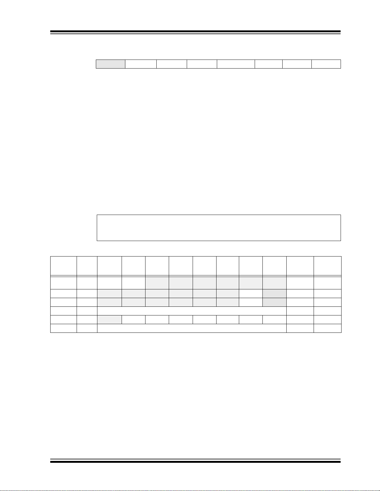
PIC16F627A/628A/648A
REGISTER 8-1: T2CON – TIMER2 CONTROL REGISTER (ADDRESS: 12h)
U-0 R/W-0 R/W-0 R/W-0 R/W-0 R/W-0 R/W-0 R/W-0
— TOUTPS3 TOUTPS2 TOUTPS1 TOUTPS0 TMR2ON T2CKPS1 T2CKPS0
bit 7 bit 0
bit 7 Unimplemented: Read as ‘0’
bit 6-3 TOUTPS<3:0>: Timer2 Output Postscale Select bits
0000 = 1:1 Postscal e Value
0001 = 1:2 Postscal e Value
•
•
•
1111 = 1:16 Postscale
bit 2 TMR2ON: Timer2 On bit
1 = Timer2 is on
0 = Timer2 is off
bit 1-0 T2CKPS<1:0>: Timer2 Clock Prescale Select bits
00 = 1:1 Prescaler Value
01 = 1:4 Prescaler Value
1x = 1:16 Prescaler Value
Legend:
R = Readable bit W = Writable bit U = Unimplemented bit, read as ‘0’
-n = Value at POR ‘1’ = Bit is set ‘0’ = Bit is cleared x = Bit is unknown
TABLE 8-1: REGISTERS ASSOCIATED WITH TIMER2 AS A TIMER/COUNTER
Address Name Bit 7 Bit 6 Bit 5 Bit 4 Bit 3 Bit 2 Bit 1 Bit 0
0Bh, 8Bh,
10Bh, 18Bh
0Ch PIR1
8Ch PIE1 EEIE CMIE RCIE TXIE — CCP1IE TMR2IE TMR1IE
11h TMR2 Timer2 Module’s Register
12h T2CON
92h PR2 Timer2 Peri od Regi ster
Legend: x = unknown , u = unchanged, - = unimplemented read as ‘0’. Shaded cells are not used by the Timer2 module.
INTCON GIE PEIE
EEIF CMIF RCIF TXIF — CCP1IF TMR2IF TMR1IF
— TOUTPS3 TOUTPS2 TOUTPS1 TOUTPS0 TMR2ON T2CKPS1 T2CKPS0
T0IE INTE RBIE T0IF INTF RBIF 0000 000x 0000 000u
Value on
POR
0000 -000 0000 -000
0000 -000 0000 -000
0000 0000 0000 0000
-000 0000 -000 0000
1111 1111 1111 1111
Value on
all other
Resets
© 2007 Microchip Technology Inc. DS40044F-page 53

PIC16F627A/628A/648A
NOTES:
DS40044F-page 54 © 2007 Microchip Technology Inc.

PIC16F627A/628A/648A
9.0 CAPTURE/COMPARE/PWM (CCP) MODULE
The CCP (Capture/Comp a r e/PW M) m od ule co nt ai ns a
16-bit register which can operate as a 16-bit Capture
register, as a 16-bit Compare register or as a PWM
master/slave Duty Cycle register. Table 9-1 shows the
timer resources of the CCP module modes.
CCP1 Module
Capture/Compare/PWM Register1 (CCPR1) is
comprised of t wo 8-bit registers: CCP R1L (low byte)
and CCPR1H (high byte). The CCP1CON register
controls the operation of CCP1. All are readable and
writable.
Additional information on the CCP module is available
in the “PIC
ual” (DS33023).
®
Mid-Range MCU Family Reference Man-
TABLE 9-1: CCP MODE – TIMER
RESOURCE
CCP Mode Timer Resource
Capture Timer1
Compare Timer1
PWM Timer2
REGISTER 9-1: CCP1CON – CCP OPERATION REGISTER (ADDRESS: 17h)
U-0 U-0 R/W-0 R/W-0 R/W-0 R/W-0 R/W-0 R/W-0
— — CCP1X CCP1Y CCP1M3 CCP1M2 CCP1M1 CCP1M0
bit 7 bit 0
bit 7-6 Unimplemented: Read as ‘0’
bit 5-4 CCP1X:CCP1Y: PWM Least Significant bits
Capture Mode
Unused
Compare Mode
Unused
PWM Mode
These bits are the two LSbs of the PWM duty cycle. The eight MSbs are found in CCPRxL.
bit 3-0 CCP1M<3:0>: CCPx Mode Select bits
0000 = Capture/Compare/PWM off (resets CCP1 module)
0100 = Capture mode, every falling edge
0101 = Capture mode, every rising edge
0110 = Capture mode, every 4th rising edge
0111 = Capture mode, every 16th r ising edge
1000 = Compare mode, set output on match (CCP1IF bit is set)
1001 = Compare mode, clear output on match (CCP1IF bit is set)
1010 = Compare mode, generate software interrupt on match (CCP1IF bit is set, CCP1 pin is
unaffected)
1011 = Compare mode, trigger special event (CCP1IF bit is set; CCP1 resets TMR1
11xx = PWM mode
Legend:
R = Readable bit W = Writable bit U = Unimplemented bit, read as ‘0’
-n = Value at POR ‘1’ = Bit is set ‘0’ = Bit is cleared x = Bit is unknown
© 2007 Microchip Technology Inc. DS40044F-page 55

PIC16F627A/628A/648A
9.1 Capture Mode
In Capture mode, CCPR1H:CCPR1L captures the
16-bit value of the TMR1 regi ster when an event occu rs
on pin RB3/CCP1. An event is defined as:
• Every falling edge
• Every rising edge
• Every 4th rising edge
• Every 16th rising edge
An event is selected by control bits CCP1M<3:0>
(CCP1CON<3:0>). When a capture is made, the
interrupt request flag bit CCP1IF (PIR1<2>) is set. It
must be cleared in software. If another capture occurs
before the value in register CCPR1 is read, the old
captured value will be lost.
9.1.1 CCP PIN CONFIGURATION
In Capture mode, the RB3/CCP1 pin should be configured as an input by setting the TRISB<3> bit.
Note: If the RB3/CCP1 is configured as an
output, a write to the port can cause a
capture condition.
FIGURE 9-1: CAPTURE MODE
OPERATION BLOCK
DIAGRAM
Set flag bit CCP1IF
Prescaler
³ 1, 4, 16
RB3/CCP1
pin
and
edge detect
CCP1CON<3:0>
Q’s
9.1.2 TIMER1 MODE SELECTION
Timer1 must be running in Timer mode or Synchronized Counter mode for the CCP module to use the
capture feature. In Asynchronous Counter mode, the
capture operation may not work.
9.1.3 SOFTWARE INTERRUPT
When the Capture mode is changed, a false capture
interrupt may be generated. The user should keep bit
CCP1IE (PIE1<2>) clear to avoid false interrupts and
should clear the flag bit CCP1IF following any such
change in Operating mode.
(PIR1<2>)
CCPR1H CCPR1L
Capture
Enable
TMR1H TMR1L
9.1.4 CCP PRESCALER
There are four prescaler settings, specified by bits
CCP1M<3:0>. Whenever the CCP module is turned
off, or the CCP module is not in Capture mode, the
prescaler counter is cleared. This means that any
Reset will clear the prescaler counter.
Switching from one capture prescaler to another may
generate an interrupt. Also, the prescaler counter will not
be cleared, therefore the first capture may be from a
non-zero prescaler. Example 9-1 shows the
recommended method for switching between capture
prescalers. This example also clears the prescaler
counter and will not generate the “false” interrupt.
EXAMPLE 9-1: CHANGING BETWEEN
CAPTURE PRESCALERS
CLRF CCP1CON ;Turn CCP module off
MOVLW NEW_CAPT_PS ;Load the W reg with
MOVWF CCP1CON ;Load CCP1CON with this
; the new prescaler
; mode value and CCP ON
; value
9.2 Compare Mode
In Compare mode, the 16-bit CCPR1 register value is
constantly compared against the TMR1 register pair
value. When a match occurs, the RB3/C CP 1 pin is:
• Driven high
•Driven low
• Remains unchanged
The action on the pin is based on the value of control
bits CCP1M<3:0> (CCP1CON<3:0>). At the same
time, interrupt flag bit CCP1IF is set.
FIGURE 9-2: COMPARE MODE
OPERATION BLOCK
DIAGRAM
Set flag bit CCP1IF
(PIR1<2>)
CCPR1H CCPR1L
QS
Output
RB3/CCP1
pin
TRISB<3>
Output Enable
Note: Special event trigger will reset Timer1, but not
set interrupt flag bit TMR1IF (PIR1<0>).
Logic
R
CCP1CON<3:0>
Mode Select
match
Comparator
TMR1H TMR1L
DS40044F-page 56 © 2007 Microchip Technology Inc.

PIC16F627A/628A/648A
9.2.1 CCP PIN CONFIGURATION
The user must configure the RB3/CCP1 pin as an
output by clearing the TRISB<3> bit.
Note: Clearing the CCP1CON register will force
the RB3/CCP1 compare output latch to
the default low level. This is not the data
latch.
9.2.4 SPECIAL EVENT TRIGGER
In this mode (CCP1M<3:0>=1011), an internal hardware trigger is generated, whi ch may be used to ini tiate
an action. See Register 9-1.
The special event trigger output of the CCP occurs
immediately upon a match between the TMR1H,
TMR1L register pair and CCPR1H, CCPR1L register
pair. The TMR1H, TMR1L register pair is not reset until
9.2.2 TIMER1 MODE SELECTION
Timer1 must be running in Timer mode or Synchronized Counter mode if the CCP module is using the
compare feature. In Asynchronous Counter mode, the
compare operation may not work.
the next rising edge of the TMR1 clock . This all ows the
CCPR1 register pair to effectively be a 16-bit programmable period register for Timer1. The special event
trigger output also starts an A/D conversion provided
that the A/D module is enabled.
Note: Removing the match condition by chang-
9.2.3 SOFTWARE INTERRUPT MODE
When generate software interrupt is chosen the CCP1
pin is not affected . Only a CCP interrup t is generated (if
enabled).
ing the contents of t he CCPR1H, CCPR1L
register pair between the clock edge that
generates the special event trigger and
the clock edge that generates the TMR1
Reset will preclude the Reset from
occuring.
TABLE 9-2: REGISTERS ASSOCIATED WITH CAPTURE, COMPARE, AND TIMER1
Address Name Bit 7 Bit 6 Bit 5 Bit 4 Bit 3 Bit 2 Bit 1 Bit 0
Value on
POR
Value on
all other
Resets
0Bh, 8Bh,
10Bh, 18Bh
0Ch PIR1
8Ch PIE1
86h, 186h TRISB PORTB Data Direction Register 1111 1111 1111 1111
0Eh TMR1L Holding Register for the Least Significant Byte of the 16-bit TMR1 Register xxxx xxxx uuuu uuuu
0Fh TMR1H Holding Register for the Most Significant Byte of the 16-bit TMR1 Register xxxx xxxx uuuu uuuu
10h T1CON
15h CCPR1L Capture/Compare/PWM Register1 (LSB) xxxx xxxx uuuu uuuu
16h CCPR1H Capture/Compare/PWM Register1 (MSB) xxxx xxxx uuuu uuuu
17h CCP1CON
Legend: x = unknown, u = unchanged, - = unimplemented read as ‘0’. Shaded cells are not used by Capture and Timer1.
INTCON GIE PEIE
EEIF CMIF RCIF TXIF — CCP1IF TMR2IF TMR1IF
EEIE CMIE RCIE TXIE — CCP1IE TMR2IE TMR1IE
— — T1CKPS1 T1CKPS0 T1OSCEN T1SYN C TM R1CS TMR1ON --00 0000 --uu uuuu
— — CCP1X CCP1Y CCP1M3 CCP1M2 CCP1M1 CCP1M0
T0IE INTE RBIE T0IF INTF RBIF 0000 000x 0000 000u
0000 -000 0000 -000
0000 -000 0000 -000
--00 0000 --00 0000
© 2007 Microchip Technology Inc. DS40044F-page 57
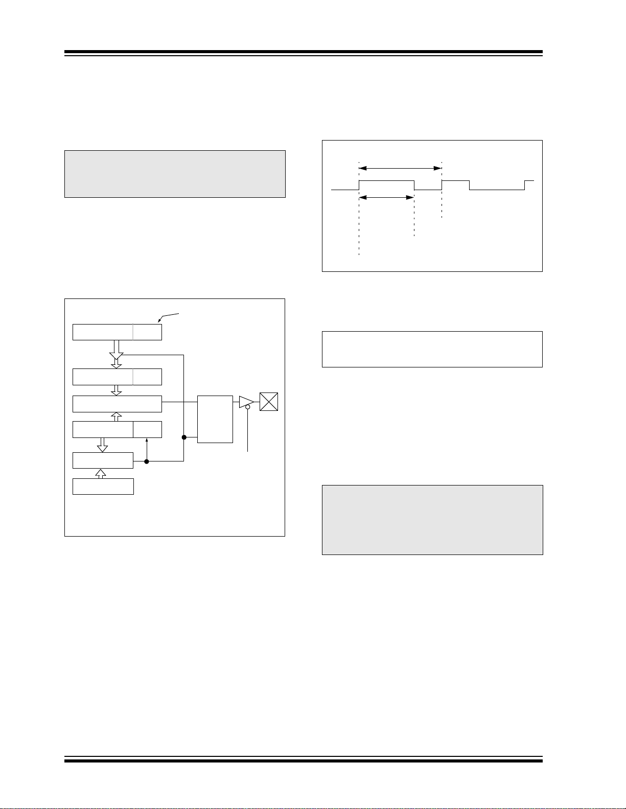
PIC16F627A/628A/648A
1
9.3 PWM Mode
In Pulse Width Modulation (PWM) mode, the CCP1 pin
produces up to a 10-bit resolution PWM output. Since
the CCP1 pin is multip lexed with the POR TB data latch,
the TRISB<3> bit must be cleared to make the CCP1
pin an output.
Note: Clearing the CCP1CON register will force
the CCP1 PWM output latch to th e de fau lt
low level. T his is not t he PORTB I /O data
latch.
Figure 9-3 shows a simplified block diagram of the
CCP module in PWM mode.
For a step by step proce dure on h ow to set up the CC P
module for PWM operation, see Section 9.3.3 “Set-
Up for PWM Operation”.
FIGURE 9-3: SIMPLIFIED PWM BLOCK
DIAGRAM
Duty cycle registers
CCPR1L
CCPR1H (Slave)
Comparator
TMR2
Comparator
PR2
Note 1: 8-bit timer is concatenated with 2-bit internal Q
(1)
Clear Timer,
CCP1 pin and
latch D.C.
clock or 2 bits of the prescaler to create 10-bit
time base.
CCP1CON<5:4>
Q
R
S
RB3/CCP
TRISB<3>
A PWM output (Figure 9-4) has a time base (period)
and a time that the output stays high (duty cycle). The
frequency of the PWM is the inverse of the period
(frequency = 1/period).
FIGURE 9-4: PWM OUTPUT
Period
Duty Cycle
TMR2 = PR2
TMR2 = Duty Cycle
TMR2 = PR2
9.3.1 PWM PERIO D
The PWM period is specified by writing to the PR2
register. The PWM period can be calculated using the
following formula:
PWM period PR2()1+[]4 ⋅⋅= Tosc TMR2 prescale⋅
value
PWM frequency is defined as 1/[PWM period].
When TMR2 is eq ual to PR2, t he following three event s
occur on the next increment cycle:
•TMR2 is cleared
• The CCP1 pin is set (exception: if PWM duty
cycle = 0%, the CCP1 pin will not be set)
• The PWM duty cycle is latc hed from CC PR1L into
CCPR1H
Note: The Timer2 postscaler (see Section 8.0
“Timer2 Module”) is not used in the
determination of the PWM frequency. The
postscaler could be used to have a servo
update rate at a different frequency than
the PWM output.
DS40044F-page 58 © 2007 Microchip Technology Inc.

PIC16F627A/628A/648A
9.3.2 PWM DUTY CYCLE
The PWM duty cycle is specified by writing to the
CCPR1L register and to the CCP1CON<5:4> bits. Up
to 10-bit resolution is available: the CCPR1L contains
the eight MSbs and the CCP1CON<5:4> contains the
two LSbs. This 10-bit value is represented by
CCPR1L:CCP1CON<5:4>. The following equation is
used to calculate the PWM duty cycle in time:
PWM duty cycle =
(CCPR1L:CCP1CON<5:4>) Tosc TMR2 prescale
CCPR1L and CCP1CON <5:4> c an be wr itten to at an y
time, but the duty cycle value is not latched into
CCPR1H until after a match between PR2 and TMR2
occurs (i.e., the period is complete). In PWM mode,
CCPR1H is a read-only register.
The CCPR1H register and a 2-bit internal latch are
used to double buf fer the PWM duty cycl e. This do uble
buffering is essential for glitchless PWM operation.
When the CCPR1H and 2-bit latch match TMR2
concatenated with an internal 2-bit Q clock or 2 bits of
the TMR2 prescaler, the CCP1 pin is cleared.
⋅⋅
value
Maximum PWM resolution (bits) for a given PWM
frequency:
PWM
Resolution
⎛⎞
-------------------------------------------------------------
log
⎝⎠
PWM TMR2 Prescaler
F
---------------------------------------------------------------------------
×
log(2)
Fosc
bits=
Note: If the PWM duty cycle value is longer tha n
the PWM per iod t he CCP 1 pin will n ot be
cleared.
For an example PWM period and duty cycle
calculation, see the PIC
®
Mid-Range Reference Man-
ual (DS33023).
9.3.3 SET-UP FOR PWM OPERATION
The following steps should be taken when configuring
the CCP module for PWM operation:
1. Set the PWM period by writing to the PR2
register.
2. Set the PWM duty cycle by writing to the
CCPR1L register and CCP1CON<5:4> bits.
3. Make the CCP1 pin an output by clearing the
TRISB<3> bit.
4. Set the TMR2 presca le value and enable T ime r2
by writing to T2CON.
TABLE 9-3: EXAMPLE PWM FREQUENCIES AND RESOLUTIONS AT 20 MHz
PWM Frequency 1.22 kHz 4.88 kHz 19.53 kHz 78.12 kHz 156.3 kHz 208.3 kHz
Timer Prescaler (1, 4, 16) 16 4 1 1 1 1
PR2 Value 0xFF 0xFF 0xFF 0x3F 0x1F 0x17
Maximum Resolution (bits) 10 10 10 8 7 6.5
TABLE 9-4: REGISTERS ASSOCIATED WITH PWM AND TIMER2
Address Name Bit 7 Bit 6 Bit 5 Bit 4 Bit 3 Bit 2 Bit 1 Bit 0
0Bh, 8Bh,
10Bh, 18Bh
0Ch PIR1
8Ch PIE1
86h, 186h TRISB TRISB7 TRISB6 TRISB5 TRISB4 TRISB3 TRISB2 TRISB1 TRISB0 1111 1111 1111 1111
11h TMR2 Timer2 Module’s Register 0000 0000 0000 0000
92h PR2 Timer2 Module’s Period Register 1111 1111 1111 1111
12h T2CON
15h CCPR1L Capture/Compare/PWM Register 1 (LSB) xxxx xxxx uuuu uuuu
16h CCPR1H Capture/Compare/PWM Register 1 (MSB) xxxx xxxx uuuu uuuu
17h CCP1CON
Legend: x = unknown, u = unchanged, - = unimplemented read as ‘0’. Shaded cells are not used by PWM and Timer2.
INTCON GIE PEIE
EEIF CMIF RCIF TXIF — CCP1IF TMR2IF TMR1IF 0000 -000 0000 -000
EEIE CMIE RCIE TXIE — CCP1IE TMR2IE TMR1IE 0000 -000 0000 -000
— TOUTPS3 TOUTPS2 TOUTPS1 TOUTPS0 TMR2ON T2CKPS1 T2CKPS0 -000 0000 uuuu uuuu
— — CCP1X CCP1Y CCP1M3 CCP1M2 CCP1M1 CCP1M0 --00 0000 --00 0000
T0IE INTE RBIE T0IF INTF RBIF 0000 000x 0000 000u
Val ue o n
POR
Val ue o n
all other
Resets
© 2007 Microchip Technology Inc. DS40044F-page 59

PIC16F627A/628A/648A
NOTES:
DS40044F-page 60 © 2007 Microchip Technology Inc.

PIC16F627A/628A/648A
10.0 COMPARATOR MODULE
The CMCON register, shown in Registe r 10-1, controls
the comparator input and output multiplexers. A block
The comparator module contains two analog
diagram of the comparator is shown in Figure 10-1.
comparators. The inputs to the comparators are
multiplexed with the RA0 through RA3 pins . The on-chip
Voltage Reference (Section 11.0 “Voltage Reference
Module”) can also be an input to the comparators.
REGISTER 10-1: CMCON – COMPARATOR CONFIGURATION REGISTER (ADDRESS: 01Fh)
R-0 R-0 R/W-0 R/W-0 R/W-0 R/W-0 R/W-0 R/W-0
C2OUT C1OUT C2INV C1INV CIS CM2 CM1 CM0
bit 7 bit 0
bit 7 C2OUT: Comparator 2 Out put bit
When C2INV =
1 = C2 VIN+ > C2 VIN0 = C2 V
When C2INV =
1 = C2 VIN+ < C2 VIN-
0 = C2 V
bit 6 C1OUT: Comparator 1 Out put bit
When C1INV = 0:
1 = C1 VIN+ > C1 VIN0 = C1 V
0:
IN+ < C2 VIN-
1:
IN+ > C2 VIN-
IN+ < C1 VIN-
When C1INV =
1:
1 = C1 VIN+ < C1 VIN0 = C1 V
IN+ > C1 VIN-
bit 5 C2INV: Comparator 2 Output Inversion bit
1 = C2 Output inverted
0 = C2 Output not inverted
bit 4 C1INV: Comparator 1 Output Inversion bit
1 = C1 Output inverted
0 = C1 Output not inverted
bit 3 CIS: Comparator Input Switch bit
When CM<2:0>: = 001
Then:
1 = C1 V
0 = C1 V
When CM<2:0> =
IN- connects to RA3
IN- connects to RA0
010
Then:
1 = C1 V
C2 V
0 = C1 V
C2 V
IN- connects to RA3
IN- connects to RA2
IN- connects to RA0
IN- connects to RA1
bit 2-0 CM<2:0>: Comparator Mode bits
Figure 10-1 shows the comparator modes and CM<2:0> bit settings
Legend:
R = Readable bit W = Writable bit U = Unimplemented bit, read as ‘0’
-n = Value at POR ‘1’ = Bit is set ‘0’ = Bit is cleared x = Bit is unknown
© 2007 Microchip Technology Inc. DS40044F-page 61

PIC16F627A/628A/648A
10.1 Comparator Configuration
There are eight modes of operation for the
If the Comparator mode is changed, the comparator
output level may not be valid for the specified mode
change delay shown in Table 17-2.
comparators. The CMCON register is used to select
the mode. Figure 10-1 shows the eight possible
Note 1: Comparator interrupts should b e disable d
modes. The TR ISA regi ste r cont rol s the data di re ction
of the comparator pins for each mode.
FIGURE 10-1: COMPARATOR I/O OPERATING MODES
Comparators Reset (POR Default Value)
CM<2:0> = 000
A
V
RA0/AN0
RA3/AN3/CMP1
RA1/AN1
RA2/AN2/V
REF
A
A
A
IN-
C1
V
IN+
IN-
V
C2
IN+
V
Two Independent Comparators
CM<2:0> = 100
A
V
RA0/AN0
RA3/AN3/CMP1
RA1/AN1
RA2/AN2/V
REF
A
A
A
IN-
C1
IN+
V
IN-
V
C2
IN+
V
Off (Read as ‘0’)
Off (Read as ‘0’)
C1V
OUT
C2VOUT
Comparators Off
CM<2:0> = 111
RA0/AN0
RA3/AN3/CMP1
RA1/AN1
RA2/AN2/V
Four Inputs Multiplexed to Two Comparators
CM<2:0> = 010
RA0/AN0
RA3/AN3/CMP1
RA1/AN1
RA2/AN2/V
during a Comparator mode change,
otherwise a false interrupt may occur.
2: Comparators can have an inverted
output. See Figure 10-1.
REF
REF
D
D
D
D
A
A
A
A
V
V
V
V
SS
V
CIS = 0
CIS = 1
CIS = 0
CIS = 1
IN-
IN+
IN-
IN+
C1
C2
Off (Read as ‘0’)
Off (Read as ‘0’)
IN-
V
C1
IN+
V
IN-
V
C2
IN+
V
From VREF
C1VOUT
C2VOUT
Module
Two Common Reference Comparators
CM<2:0> = 011
RA0/AN0
RA3/AN3/CMP1
RA1/AN1
RA2/AN2/V
REF
A
D
A
A
IN-
V
C1
IN+
V
IN-
V
C2
IN+
V
One Independent Comparator
CM<2:0> = 101
RA0/AN0
RA3/AN3/CMP1
D
D
IN-
V
C1
IN+
V
VSS
RA1/AN1
RA2/AN2/V
REF
A
A
IN-
V
C2
IN+
V
A = Analog Input, port reads zeros always.
C1VOUT
C2VOUT
Off (Read as ‘0’)
OUT
C2V
D = Digital Input.
Two Common Reference Comparators with Outputs
CM<2:0> = 110
RA0/AN0
RA3/AN3/CMP1
RA1/AN1
RA2/AN2/V
REF
RA4/T0CKI/CMP2
A
D
A
A
Open Drain
IN-
V
C1
IN+
V
IN-
V
C2
IN+
V
Three Inputs Multiplexed to Two Comparators
CM<2:0> = 001
REF
A
V
CIS = 0
A
CIS = 1
A
A
IN-
C1
IN+
V
IN-
V
C2
IN+
V
RA0/AN0
RA3/AN3/CMP1
RA1/AN1
RA2/AN2/V
CIS (CMCON<3>) is the Comparator Input Switch.
C1VOUT
C2VOUT
C1VOUT
C2VOUT
DS40044F-page 62 © 2007 Microchip Technology Inc.

PIC16F627A/628A/648A
The code exam ple in Exampl e 10-1 depicts th e steps
required to configur e the Compara tor module. RA 3 and
RA4 are configured a s digi tal outpu t. RA0 and R A1 are
configured as the V- inputs and RA 2 as the V+ inp ut to
both comparators.
EXAMPLE 10-1: INITIALIZING
COMPARATOR MODULE
FLAG_REG EQU 0X20
CLRF FLAG_REG ;Init flag register
CLRF PORTA ;Init PORTA
MOVF CMCON, W ;Load comparator bits
ANDLW 0xC0 ;Mask comparator bits
IORWF FLAG_REG,F ;Store bits in flag register
MOVLW 0x03 ;Init comparator mode
MOVWF CMCON ;CM<2:0> = 011
BSF STATUS,RP0 ;Select Bank1
MOVLW 0x07 ;Initialize data direction
MOVWF TRISA ;Set RA<2:0> as inputs
BCF STATUS,RP0 ;Select Bank 0
CALL DELAY10 ;10µs delay
MOVF CMCON,F ;Read CMCON to end change
BCF PIR1,CMIF ;Clear pending interrupts
BSF STATUS,RP0 ;Select Bank 1
BSF PIE1,CMIE ;Enable comparator interrupts
BCF STATUS,RP0 ;Select Bank 0
BSF INTCON,PEIE ;Enable peripheral interrupts
BSF INTCON,GIE ;Global interrupt enable
;RA<4:3> as outputs
;TRISA<7:5> always read ‘0’
;condition
10.2 Comparator Operation
A single compa rator is sho wn i n Fig ure 10-2 along with
the relationship between the analog input levels and
the digital output . When the analo g input a t V
than the analog input V
IN-, the output of the compara tor
is a digital low level. When the analog input at V
greater than the analog input V
IN-, the output of the
comparator is a digital high level. The shaded areas of
the output of the comparator in Figure 10-2 represent
the uncertainty due to input offsets and response time.
See Table 17-2 for Common Mode voltage.
IN+ is less
IN+ is
FIGURE 10-2: SINGLE COMPARATOR
VIN-
VIN+
Result
VIN+
IN-
V
+
Result
–
10.3.1 EXTERNAL REFERENCE SIGNAL
When external voltage references are used, the
Comparator module can be configured to have the
comparators operate from the same or different
reference sources. However, threshold detector
applications may require the same reference. The
reference signal must be between V
SS and VDD, and
can be applied to either pin of the comparator(s).
10.3.2 INTERNAL REFERENCE SIGNAL
The Comparator mo dule also allows the selection of an
internally generated voltage reference for the
comparators. Section 11.0 “Voltage Reference
Module”, contains a det ailed descripti on of t he Voltag e
Reference module that provides this signal. The
internal reference signa l is used when the comp arators
are in mode CM<2:0> = 010 (Figure10-1). In this
mode, the internal voltage reference is applied to the
IN+ pin of both comparators.
V
10.3 Comparator Reference
An external or internal reference signal may be used
depending on the comparator Operating mode. The
analog signal that is pre se nt at V
signal at V
IN+, and the digital output of the comparator
is adjusted accordingly (Figure 10-2).
IN- is compared to the
10.4 Comparator Response Time
Response time is the minimum time, after selecting a
new reference voltage or input source, before the
comparator output is to have a valid level. If the internal
reference is changed, the maximum delay of the internal
voltage reference must be considered when using the
comparator outputs. Otherwise, the maximum delay of
the comparators should be used (Table 17-2, page 140).
© 2007 Microchip Technology Inc. DS40044F-page 63

PIC16F627A/628A/648A
10.5 Comparator Outputs
The comparator outputs are read through the CMCON
register. These bits are read-only. The comparator
outputs may also be directly output to the RA3 and RA4
I/O pins. When the CM<2:0> = 110 or 001, multiplexors
in the output path of the RA3 and RA4/T0CK1/CMP2
pins will switch and the output of each pin will be the
unsynchronized output of the comparator. The
uncertainty of each of the comparators is related to the
input offset voltage and the response time given in the
specifications. Figure 10-3 shows the comparator output
block diagram.
The TRISA bits will still function as an output enable/
disable for the RA3/AN3/CMP1 and RA4/T0CK1/
CMP2 pins while in this mode.
Note 1: When reading the PORT register, all pins
configured as anal og inp ut s will read as a
‘0’. Pins configured as digital inputs will
convert an analog input, according to the
Schmitt Trigger input specification.
2: Analog le vels on any pin that is defined a s
a digital input may cause the input buffer
to consume more current than is
specified.
FIGURE 10-3: MODIFIED COMPARATOR OUTPUT BLOCK DIAGRAM
CnINV
To RA3/AN3/CMP1 or
RA4/T0CK1/CMP2 pin
To Data Bus
CMCON<7:6>
RD CMCON
Set CMIF bit
From other Comparator
EN
DQ
CL
DQ
EN
Reset
CnVOUT
Q3
Q1
DS40044F-page 64 © 2007 Microchip Technology Inc.

PIC16F627A/628A/648A
10.6 Comparator Interrupts
The comparator interrupt flag is set whenever there is
a change in the output value of either comparator.
Software will need to maintain information about the
status of the out put bits, as rea d from CMCON<7 :6>, to
determine the actual change that has occurred. The
CMIF bit, PIR1<6>, is the comparator interrupt flag.
The CMIF bit must be reset by clearing ‘0’. Since it is
also possible to write a ‘1’ to this register, a simulated
interrupt may be initiated.
The CMIE bit (PIE1<6>) and the PEIE bit
(INTCON<6>) must be set to enable the interrupt. In
addition, the GIE bit must also be set. If any of these
bits are clear, the interrupt is not enabled, though the
CMIF bit will still be set if an interr upt co nd itio n occ urs .
Note: If a change in the CMCON register
(C1OUT or C2OUT) should occur when a
read operation is being executed (start of
the Q2 cycle), then the CMIF (PIR1<6>)
interrupt flag may not get set.
The user, in the inte r ru pt se rvi c e r o uti ne , ca n clea r t he
interrupt in the following manne r :
a) Any write or read of CMCON. This will end the
mismatch condition.
b) Clear flag bit CMIF.
A mismatch condition will co nti nue to set fla g bit CMIF.
Reading CMCON will end the mismatch condition and
allow flag bit CMIF to be cleared.
10.7 Comparator Operation During Sleep
When a comparator is active and the device is placed
in Sleep mode, the comparator remains active and the
interrupt is functional if enabled. This interrupt will
wake-up the de vice from Sleep mo de when enabled.
While the comparator is powered-up, higher Sleep
currents than shown in the power-down current
specification will occur. Each comparator that is
operational will cons ume additional cu rrent as shown in
the comparator specifications. To minimize power
consumption while in Sleep mode, turn off the
comparators, CM<2:0>= 111, before entering Sleep. If
the device wakes up from Sleep, the contents of the
CMCON register are not affected.
10.8 Effects of a Reset
A device Reset forces the CMCON register to its Reset
state. This forces the Comparator module to be in the
comparator Reset mode, CM<2:0> = 000. This ensures
that all potential inputs are analog inpu ts. Device current
is minimized when analog inputs are present at Reset
time. The comparators will be pow ered-down during the
Reset interval.
10.9 Analog Input Connection Considerations
A simplified circuit for an analog input is shown in
Figure 10-4. Since the analog pins are connected to a
digital output, they have reverse biased diodes to VDD
and VSS. The analog i npu t the r efo re, m us t b e b etween
SS and VDD. If the input voltage deviates from this
V
range by more than 0.6V in either direction, one of the
diodes is forward biased and a latch-up may occur. A
maximum source impedance of 10 kΩ is
recommended for the analog sources. Any external
component connected to an analog input pin, such as
a capacitor or a Zener diode, should have very little
leakage current.
© 2007 Microchip Technology Inc. DS40044F-page 65

PIC16F627A/628A/648A
FIGURE 10-4: ANALOG INPUT MODE
VDD
R
VA
S < 10 K
VT = 0.6V
IN
A
CPIN
5pF
VT = 0.6V
ILEAKAGE
±500 nA
V
SS
RIC
Legend: CPIN = Input Capacitance
V
T = Threshold Voltage
LEAKAGE = Leakage Current at the Pin
I
IC = Inter connect Resistance
R
R
S = Source Impedance
VA = Analog Voltage
TABLE 10-1: REGISTERS ASSOCIATED WITH COMPARATOR MODULE
Address Name Bit 7 Bit 6 Bit 5 Bit 4 Bit 3 Bit 2 Bit 1 Bit 0
1Fh CMCON C2OUT C1OUT C2INV C1NV CIS CM2 CM1 CM0 0000 0000 0000 0000
0Bh, 8Bh,
10Bh, 18Bh
0Ch PIR1
8Ch PIE1
85h TRISA
Legend: x = Unknown, u = Unchanged, - = Unimplemented, read as ‘0’
INTCON GIE PEIE
EEIF CMIF RCIF TXIF — CCP1IF TMR2IF TMR1IF 0000 -000 0000 -000
EEIE CMIE RCIE TXIE — CCP1IE TMR2IE TMR1IE 0000 -000 0000 -000
TRISA7 TRISA6 TRISA5 TRISA4 TRISA3 TRISA2 TRISA1 TRISA0 1111 1111 1111 1111
T0IE INTE RBIE T0IF INTF RBIF 0000 000x 0000 000u
Val ue on
POR
Value on
All Other
Resets
DS40044F-page 66 © 2007 Microchip Technology Inc.

PIC16F627A/628A/648A
11.0 VOLTAGE REFERENCE MODULE
The Voltage Reference module consists of a 16-tap
resistor ladder network that provides a selectable voltage reference. The re sistor ladde r is segmented to provide two ranges of V
function to conserve power when the reference is not
being used. The VRCON register controls the operation of the reference as shown in Figure 11-1. The
block diagram is given in Figure 11-1.
11.1 Voltage Reference Configuration
The Voltage Reference module can output 16 distinct
voltage levels for each range.
REF values and has a po wer-d ow n
The equations used to calculate the output of the
Voltage Reference module are as fol lows :
if VRR = 1:
VR<3:0>
VREF
if VRR = 0:
VREF VDD
=
The setting tim e of the V ol tage Re ference m odule m ust
be considered when changing the V
(Table 17-3). Example 11-1 demonstrates how voltage
reference is configured for an output voltage of 1.25V
DD = 5.0V.
with V
---------------------- -
=
24
VR<3:0>
⎛⎞
⎝⎠
1
-- -
-----------------------
×
+V
4
DD
×
V
×
32
REF output
DD
REGISTER 11-1: VRCON – VOLTAGE REFERENCE CONTROL REGISTER (ADDRESS: 9Fh)
R/W-0 R/W-0 R/W-0 U-0 R/W-0 R/W-0 R/W-0 R/W-0
VREN VROE VRR — VR3 VR2 VR1 VR0
bit 7 bit 0
bit 7 VREN: V
1 = VREF circuit powered on
0 = V
bit 6 VROE: V REF Output Enable bit
1 = VREF is output on RA2 pin
0 = V
bit 5 VRR: V
1 = Low range
0 = High range
bit 4 Unimplemented: Read as ‘0’
bit 3-0 VR<3:0>: V
When VRR = 1: VREF = (VR<3:0>/ 24) * VDD
When VRR = 0: VREF = 1/4 * VDD + (VR<3:0>/ 32) * VDD
REF Enable bit
REF circuit powered down, no IDD drain
REF is disconnected from RA2 pin
REF Range Selection bit
REF Value Selection bits 0 ≤ VR <3:0> ≤ 15
Legend:
R = Readable bit W = Writable bit U = Unimplemented bit, read as ‘0’
-n = Value at POR ‘1’ = Bit is set ‘0’ = Bit is cleared x = Bit is unknown
© 2007 Microchip Technology Inc. DS40044F-page 67

PIC16F627A/628A/648A
FIGURE 11-1: VOLTAGE REFERENCE BLOCK DIAGRAM
VDD
16 Stages
VREN
V
REF
Note: R is defined in Table 17-3.
8R
R
R
EXAMPLE 11-1: VOLTAGE REFERENCE
CONFIGURATION
MOVLW 0x02 ;4 Inputs Muxed
MOVWF CMCON ;to 2 comps.
BSF STATUS,RP0 ;go to Bank 1
MOVLW 0x07 ;RA3-RA0 are
MOVWF TRISA ;outputs
MOVLW 0xA6 ;enable V
MOVWF VRCON ;low range set VR<3:0>=6
BCF STATUS,RP0 ;go to Bank 0
CALL DELAY10 ;10μs delay
REF
11.2 Voltage Reference Accuracy/Error
The full range of VSS to VDD cannot be realized due to
the construction of the module. The transistors on the
top and bottom of the resistor ladder network
(Figure 11-1) keep V
The Voltage Reference module is V
therefore, the V
V
DD. The tested absolute accuracy of the Voltage Ref-
erence module can be found in Table 17-3.
REF from approach ing VSS or VDD.
DD derived and
REF output changes with fluctuations in
R
16-1 Analog Mux
R
8R
VSS VSS
V
R3
(From VRCON<3:0>)
V
R0
11.5 Connection Considerations
The Voltage Reference module operates independently
of the Comparator module. The output of the reference
generator may be connected to the RA2 pin if the
TRISA<2> bit is set and the VROE bit, VRCON<6>, is
set. Enabling the V oltage R eference module output onto
the RA2 pin with an input signal present will increase
current consumption. Connecting RA2 as a digital output
REF enabled will also increase current consump-
with V
tion.
The RA2 pin can be used as a simple D/A output with
limited drive capability. Due to the limited drive
capability, a buf fer must be used in conju nction with the
Voltage Reference module output for external connections to V
technique.
REF. Figure 11-2 shows an example buffering
VRR
11.3 Operation During Sleep
When the device wakes up from Sleep through an
interrupt or a Watchdog T i mer time out, the conten t s of
the VRCON register are not affected. To minimize
current consumption in Sleep mode, the Voltage
Reference module should be disabled.
11.4 Effects of a Reset
A device Reset disa bles the V o ltage Refere nce module
by clearing bit VREN (VRCON<7>). This Reset also
disconnects the reference from the RA2 pin by clearing
bit VROE (VRCON<6>) and selects the high voltage
range by clearing bit VRR (VRCON<5>). The VREF
value select bits, VRCON<3:0>, are also cleared.
DS40044F-page 68 © 2007 Microchip Technology Inc.

PIC16F627A/628A/648A
FIGURE 11-2: VOLTAGE REFERENCE OUTPUT BUFFER EXAMPLE
(1)
VREF
Module
Note 1: R is dependent upon the voltage reference configuration VRCON<3:0> and VRCON<5>.
R
Voltage
Reference
Output
Impedance
RA2
Op Amp
+
VREF Output
TABLE 11-1: REGISTERS ASSOCIATED WITH VOLTAGE REFERENCE
Address Name Bit 7 Bit 6 Bit 5 Bit 4 Bit 3 Bit 2 Bit 1 Bit 0
9Fh VRCON VREN VROE VRR
1Fh CMCON
85h TRISA
Legend: - = Unimplemented, read as ‘0’.
C2OUT C1OUT C2INV C1INV CIS CM2 CM1 CM0 0000 0000 0000 0000
TRISA7 TRISA6 TRISA5 TRISA4 TRISA3 TRISA2 TRISA1 TRISA0 1111 1111 1111 1111
— VR3 VR2 VR1 VR0 000- 0000 000- 0000
Value On
POR
Value On
All Other
Resets
© 2007 Microchip Technology Inc. DS40044F-page 69

PIC16F627A/628A/648A
NOTES:
DS40044F-page 70 © 2007 Microchip Technology Inc.

PIC16F627A/628A/648A
12.0 UNIVERSAL SYNCHRONOUS ASYNCHRONOUS RECEIVER T RANSMITTER (USART) MODULE
The Universal Synchronous Asynchronous Receiver
Transmitter (USART) is also known as a Serial
Communicat ions Interface (S CI). The USART can be
configured as a full-duplex asynchronous system that
can communicate with peripheral device s such as CRT
terminals and personal computers, or it can be
configured as a half-duplex synchronous system that
can communicate with peripheral devices such as A/D
or D/A integrated circuits, Serial EEPROMs, etc.
The USART can be configured in the following modes:
• Asynchronous (full-duplex)
• Synchronous
• Synchronous
Bit SPEN (RCSTA<7>) and bits TRISB<2:1> have to be
set in order to configure pins RB2/TX/CK and RB1/RX/DT
as the Universal Synchronous Asynchronous Receiver
Transmitter .
Register 12-1 shows the Transmit Status and Control
Register (TXSTA) and Register 12-2 shows the
Receive Status and Control Register (RCSTA).
– Master (half-duplex)
– Slave (half-duplex)
REGISTER 12-1: TXSTA – T RANSMIT STATUS AND CONTROL REGISTER (ADDRESS: 98h)
R/W-0 R/W-0 R/W-0 R/W-0 U-0 R/W-0 R-1 R/W-0
CSRC TX9 TXEN SYNC
bit 7 bit 0
bit 7 CSRC: Cloc k Source Sele ct bit
Asynchronous mode
Don’t care
Synchronous mode
1 = Master mode (Clock generated internally from BRG)
0 = Slave mode (Clock from external source)
bit 6 TX9: 9-bit Transmit Enable bit
1 = Selects 9-bit transmission
0 = Selects 8-bit transmission
bit 5 TXEN: Transmit Enable bit
1 = Transmit enabled
0 = Transmit disabled
bit 4 SYNC: USART Mode Select bit
1 = Synchronous mode
0 = Asynchronous mode
bit 3 Unimplemented: Read as ‘0’
bit 2 BRGH: High Baud Rate Select bit
Asynchronous mode
1 = High speed
0 = Low speed
Synchronous mode
Unused in this mode
bit 1 TRMT: Transmit Shift Register Status bit
1 = TSR empty
0 = TSR full
bit 0 TX9D: 9th bit of transmit data. Can be parity bit.
Note 1: SREN/CREN overrides TXEN in SYNC mode.
(1)
— BRGH TRMT TX9D
Legend:
R = Readable bit W = Writable bit U = Unimplemented bit, read as ‘0’
-n = Value at POR ‘1’ = Bit is set ‘0’ = Bit is cleared x = Bit is unknown
© 2007 Microchip Technology Inc. DS40044F-page 71

PIC16F627A/628A/648A
REGISTER 12-2: RCST A – RECEIVE STATUS AND CONTROL REGISTER (ADDRESS: 18h)
R/W-0 R/W-0 R/W-0 R/W-0 R/W-0 R-0 R-0 R-x
SPEN RX9 SREN CREN ADEN FERR OERR RX9D
bit 7 bit 0
bit 7 SPEN: Serial Port Enable bit
(Configures RB1/RX/DT and RB2/TX/CK pins as seri al port pins when bits TRISB<2:1 > are set)
1 = Serial port enabled
0 = Serial port disabled
bit 6 RX9: 9-bit Receive Enable bit
1 = Selects 9-bit reception
0 = Selects 8-bit reception
bit 5 SREN: Single Receive Enable bit
Asynchronous mode
Don’t care
Synchronous mode - master:
1 = Enables single receive
0 = Disables single receive
This bit is cleared after reception is complete.
Synchronous mode - slave
Unused in this mode
bit 4 CREN: Continuous Receive Enable bit
Asynchronous mode
1 = Enables continuous rec e iv e
0 = Disables continuous receive
Synchronous mode
1 = Enables continuous receive until enable bit CREN is cleared (CREN overrides SREN)
0 = Disables continuous receive
bit 3 ADEN: Address Detect Enable bit
Asynchronous mode 9-bit (RX9 = 1):
1 = Enables address det ection, enabl e interrupt and lo ad of the receive bu ffer when R SR<8>
is set
0 = Disables address detec tion, all byt es are rece ived, and ni nth bit can be us ed as pari ty bit
Asynchronous mode 8-bit (RX9 =
Unused in this mode
Synchronous mode
Unused in this mode
bit 2 FERR: Framing Error bit
1 = Framing error (Can be updated by reading RCREG register and receive next valid byte)
0 = No framing error
bit 1 OERR: Overrun Error bit
1 = Overrun error (Can be cleared by clearing bit CREN)
0 = No overrun error
bit 0 RX9D: 9th bit of received data (Can be parity bit)
:
:
:
:
0):
Legend:
R = Readable bit W = Writable bit U = Unimplemented bit, read as ‘0’
-n = Value at POR ‘1’ = Bit is set ‘0’ = Bit is cleared x = Bit is unknown
DS40044F-page 72 © 2007 Microchip Technology Inc.

PIC16F627A/628A/648A
12.1 USART Baud Rate Generator (BRG)
The BRG supports both the Asynchronous and
Synchronous modes of the USART. It is a dedicated
8-bit baud rate generator. The SPBRG register
controls the period of a free running 8-bit timer. In
Asynchronous mode, bit BRGH (TXSTA<2>) also
controls the baud rate. In Synchronous mode, bit
BRGH is ignored. Table 12 -1 shows the formula for
computation of the baud rate for different USART
modes, which only apply in Master mode (internal
clock).
Given the desired baud rate and F
integer value for the SPBRG register can be calculated
using the formula in Table 12-1. From this, the error in
baud rate can be determined.
Example 12-1 shows the calculation of the baud rate
error for the following conditions:
OSC = 16 MHz
F
Desired Baud Rate = 9600
BRGH = 0
SYNC = 0
OSC, the nearest
EQUATION 12-1: CALCULATING BAUD
RATE ERROR
Fosc
Desired Baud Rate
9600
=
x25.042=
Calculate d Baud Rate
(Calculated Baud Rate - Desired Baud Rate)
Error
It may be advantageous to use the high baud rate
(BRGH = 1) even for slower baud clocks. This is
because the FOSC/(16(X + 1)) equation c an red uce th e
baud rate error in some cases.
Writing a new value to the SPBRG register causes the
BRG timer to be reset (or cleared) and ensures the
BRG does not wait for a timer overflow before
outputting the new baud rate.
The data on the RB 1/RX/DT p in is sampl ed three ti mes
by a majority detect circuit to determine if a high or a
low level is present at the RX pin.
-----------------------------------------------------------------------------------------------------------
=
=
Desired Baud Rate
9615 9600–
----------------------------- 9600
-----------------------
=
64 x 1+()
16000000
-----------------------64 x 1+()
16000000
-------------------------- 64 25 1+()
0.16%=
9615==
TABLE 12-1: BAUD RATE FORMULA
SYNC BRGH = 0 (Low Speed) BRGH = 1 (High Speed)
0 (Asynchronous) Baud Rate = F
1 (Synchronous) Baud Rate = F
Legend: X = value in SPBRG (0 to 255)
TABLE 12-2: REGISTERS ASSOCIATED WITH BAUD RATE GENERATOR
Address Name Bit 7 Bit 6 Bit 5 Bit 4 Bit 3 Bit 2 Bit 1 Bit 0
98h TXSTA
18h RCSTA SPEN
99h SPBRG Baud Rate Generator Register 0000 0000 0000 0000
Legend: x = unknown, - = unimplemented read as ‘0’. Shaded cells are not used for the BRG.
© 2007 Microchip Technology Inc. DS40044F-page 73
CSRC TX9 TXEN SYNC —BRGHTRM T TX9D 0000 -010 0000 -010
RX9 SREN CREN ADEN FERR OERR RX9D 0000 000x 0000 000x
OSC/(64(X+1)) Baud Rate = FOSC/(16(X+1))
OSC/(4(X+1)) NA
Val ue on
POR
Value on all
other Resets

PIC16F627A/628A/648A
TABLE 12-3: BAUD RATES FOR SYNCHRONOUS MODE
OSC = 20 MHz SPBRG
BAUD
RATE (K)
0.3NA——NA——NA— —
1.2NA——NA——NA— —
2.4NA——NA——NA— —
9.6 NA — — NA — — 9.766 +1.73% 255
19.2 19.53 +1.73% 255 19.23 +0.16% 207 19.23 +0.16% 129
76.8 76.92 +0.16% 64 76.92 +0.16% 51 75.76 -1.36% 32
96 96.15 +0.16% 51 95.24 -0.79% 41 96.15 +0.16% 25
300 294.1 -1.96 16 307.69 +2.56% 12 312.5 +4.17% 7
500 500 0 9 500 0 7 500 0 4
HIGH 5000 — 0 4000 — 0 2500 — 0
LOW 19.53 — 255 15.625 — 255 9.766 — 255
F
KBAUD ERROR KBAUD ERROR KBAUD ERROR
value
(decimal)
16 MHz SPBRG
value
(decimal)
10 MHz SPBR G
value
(decimal)
OSC = 7.15909 MHz SPBRG
BAUD
RATE (K)
0.3NA——NA——NA— —
1.2NA——NA——NA— —
2.4NA——NA——NA— —
9.6 9.622 +0.23% 185 9.6 0 131 9.615 +0.16% 103
19.2 19.24 +0.23% 92 19.2 0 65 19.231 +0.16% 51
76.8 77.82 +1.32 22 79.2 +3.13% 15 75.923 +0.16% 12
96 94.20 -1.88 18 97.48 +1.54% 12 1000 +4.17% 9
300 298.3 -0.57 5 316.8 5.60% 3 NA
500 NA — — NA
HIGH 1789.8 — 0 1267 — 0 100 — 0
LOW 6.991 — 255 4.950 — 255 3.906 — 255
F
KBAUD ERROR KBAUD ERROR KBAUD ERROR
value
(decimal)
5.0688 MHz SPBRG
value
(decimal)
—
—NA——
4 MHz SPBRG
value
(decimal)
—
—
OSC = 3.579545 MHz SPBRG
BAUD
RATE (K)
0.3 NA — — NA — — 0.303 +1.14% 26
1.2 NA — — 1.202 +0.16% 207 1.170 -2.48% 6
2.4 NA — — 2.404 +0.16 % 103 NA
9.6 9.622 +0.23% 92 9.615 +0.16% 25 NA — —
19.2 19.04 -0.83% 46 19.24 +0.16% 12 NA — —
76.8 74.57 -2.90% 11 83.34 +8.51% 2 NA —
96 99.43 +3.57% 8 NA
300 298.3 0.57% 2 NA — — NA — —
500 NA
HIGH 894.9 — 0 250 — 0 8.192 — 0
LOW 3.496 — 255 0.9766 — 255 0.032 — 255
F
KBAUD ERROR KBAUD ERROR KBAUD ERROR
—
value
(decimal)
1 MHz SPBRG
value
(decimal)
——
—NA——NA——
32.768 kHz SPBRG
——
NA
—
value
(decimal)
—
—
DS40044F-page 74 © 2007 Microchip Technology Inc.

PIC16F627A/628A/648A
TABLE 12-4: BAUD RATES FOR ASYNCHRONOUS MODE (BRGH = 0)
OSC = 20 MHz SPBRG
BAUD
RATE (K)
0.3NA——NA ——NA ——
1.2 1.221 +1.73% 255 1.202 +0.16% 207 1.202 +0.16% 129
2.4 2.404 +0.16% 129 2.404 +0.16% 103 2.404 +0.16% 64
9.6 9.469 -1.36% 32 9.615 +0.16% 25 9.766 +1.73% 15
19.2 19.53 +1.73% 15 19.23 +0.16% 12 19.53 +1.73V 7
76.8 78.13 +1.73% 3 83.33 +8.51% 2 78.13 +1.73% 1
96 104.2 +8.51% 2 NA — — NA — —
300 312.5 +4.17% 0 NA — — NA — —
500 NA — — NA — — NA — —
HIGH 312.5 — 0 250 — 0 156.3 — 0
LOW 1.221 — 255 0.977 — 255 0.6104 — 255
F
KBAUD ERROR KBAUD ERROR KBAUD ERROR
value
(decimal)
16 MHz SPBRG
value
(decimal)
10 MHz SPBR G
value
(decimal)
OSC = 7.15909 MHz SPBRG
BAUD
RATE (K)
0.3 NA — — 0.31 +3.13% 255 0.3005 -0.17% 207
1.2 1.203 +0.23% 92 1.2 0 65 1.202 +1.67% 51
2.4 2.380 -0.83% 46 2.4 0 32 2.404 +1.67% 25
9.6 9.322 -2.90% 11 9.9 +3.13% 7 NA — —
19.2 18.64 -2.90% 5 19.8 +3.13% 3 NA — —
76.8 NA — — 79.2 +3.13% 0 NA — —
96 NA — — NA — — NA — —
300 NA — — NA — — NA — —
500 NA — — NA — — NA — —
HIGH 111.9 — 0 79.2 — 0 62.500 — 0
LOW 0.437 — 255 0.3094 — 255 3.906 — 255
F
KBAUD ERROR KBAUD ERROR KBAUD ERROR
value
(decimal)
5.0688 MHz SPBRG
value
(decimal)
4 MHz SPBRG
value
(decimal)
OSC = 3.579545 MHz S PBRG
BAUD
RATE (K)
0.3 0.301 +0.23% 185 0.300 +0.16% 51 0.256 -14.67% 1
1.2 1.190 -0.83% 46 1.202 +0.16% 12 NA — —
2.4 2.432 +1.32% 22 2.232 -6.99% 6 NA — —
9.6 9.322 -2.90% 5 NA — — NA — —
19.2 18.64 -2.90% 2 NA — — NA — —
76.8NA——NA——NA— —
96 NA — — NA — — NA — —
300 NA — — NA — — NA — —
500 NA — — NA — — NA — —
HIGH 55.93 — 0 15.63 — 0 0.512 — 0
LOW 0.2185 — 255 0.0610 — 255 0.0020 — 255
F
KBAUD ERROR KBAUD ERROR KBAUD ERROR
value
(decimal)
1 MHz SPBRG
value
(decimal)
32.768 kHz SPBRG
value
(decimal)
© 2007 Microchip Technology Inc. DS40044F-page 75

PIC16F627A/628A/648A
TABLE 12-5: BAUD RATES FOR ASYNCHRONOUS MODE (BRGH = 1)
OSC = 20 MHz SPBRG
BAUD
RATE (K)
9600 9.615 +0.16% 129 9.615 +0.16% 103 9.615 +0.16% 64
19200 19. 230 +0.16% 64 19.230 +0.16% 51 18.939 -1.36% 32
38400 37. 878 -1.36% 32 38.461 +0.16% 25 39.062 +1.7% 15
57600 56. 818 -1.36% 21 58.823 +2.12% 16 56.818 -1.36% 10
115200 113.636 -1.36% 10 111.111 -3.55% 8 125 +8.5 1% 4
250000 250 0 4 250 0 3 NA — —
625000 625 0 1 NA — — 625 0 0
1250000 1250 0 0 NA — — NA — —
F
KBAUD ERROR KBAUD ERROR KBAUD ERROR
value
(decimal)
16 MHz SPBRG
value
(decimal)
10 MHz SPBR G
value
(decimal)
OSC = 7.16 MHz SPBRG
BAUD
RATE (K)
9600 9.520 -0.83% 46 9598.485 0.016% 32 9615.385 0.160% 25
19200 19. 454 +1.32% 22 18632.35 -2. 956% 16 19230.77 0.160% 12
38400 37.286 -2.90% 11 39593.75 3.109% 7 35714.29 -6.994% 6
57600 55. 930 -2.90% 7 52791.67 -8.348% 5 62500 8.507% 3
115200 111.860 -2.90% 3 105583.3 -8.348% 2 125000 8.507% 1
250000 NA — — 316750 26.700% 0 250000 0.000% 0
625000 NA — — NA — — NA — —
1250000 NA — — NA — — NA — —
F
KBAUD ERROR KBAUD ERROR KBAUD ERROR
value
(decimal)
5.068 MHz SPBRG
value
(decimal)
4 MHz SPBRG
value
(decimal)
OSC = 3.579 MHz SPBRG
BAUD
RATE (K)
9600 9725. 543 1.308% 22 8.928 -6.994% 6 NA NA NA
19200 18640.63 -2.913% 11 20833.3 8.507% 2 NA NA NA
38400 37281.25 -2.913% 5 31250 -18.620% 1 NA NA NA
57600 55921.88 -2.913% 3 62500 +8.507 0 NA NA NA
115200 111243.8 -2.913% 1 NA — — NA NA NA
250000 223687.5 -10.525% 0 NA — — NA NA NA
625000 NA — — NA — — NA NA NA
1250000 NA — — NA — — NA NA NA
F
KBAUD ERROR KBAUD ERROR KBAUD ERROR
value
(decimal)
1 MHz SPBRG
value
(decimal)
32.768 kHz SPBRG
value
(decimal)
DS40044F-page 76 © 2007 Microchip Technology Inc.

PIC16F627A/628A/648A
12.2 USART Asynchronous Mode
In this mode, the USART uses standard non-return-tozero (NRZ) format (one Start bit, eight or nine data bits
and one Stop bit). The most common data format is
8-bit. A dedicated 8-bit baud rate generator is used to
derive baud rate frequencies from the oscillator. The
USART transmits and receives the LSb first. The
USART’s transmitter and receiver are functionally
independent, but use the same data format and baud
rate. The baud rate generator produces a clock either
x16 or x64 of the bit shift rate, depending on bit BRGH
(TXSTA<2>). Parity is not supported by the hardware,
but can be implemente d in so ftw are (and sto red as th e
ninth data bit ). Asynchro nous mode is st opped dur ing
Sleep.
Asynchronous mode is selected by clearing bit SYNC
(TXSTA<4>).
The USART Asynchronous module consists of the
following important elements:
• Baud Rate Generator
• Sampling Circuit
• Asynchronous Transmitter
• Asynchronous Receiver
12.2.1 USART ASYNCHRONOUS TRANSMITTER
The USART transmitter block diagram is shown in
Figure 12-1. The heart of the transmitter is the T ransmit
(serial) Shift Register (TSR). The shift register obtains
its data from the read/write transmit buffer, TXREG . The
TXREG register is loaded with data in software. The
TSR register is not loaded until the Stop bit has been
transmitted from the previ ous load. As soon as the S top
bit is transmitted, t he TSR is l oaded wi th new dat a from
the TXREG register (if available). Once the TXREG
register transfers the data to the TSR register (occurs
in one T
TXIF (PIR1<4>) is set. This interrupt can be enabled/
disabled by setting/clearing enable bit TXIE
( PIE1<4>). Flag bit TXIF will be set regardless of the
state of enable bit TXIE and cannot be cleared in
software. It will res et on ly w hen n ew dat a is load ed in to
the TXREG register. While flag bit TXIF indicated the
status of the TXREG register, another bit TRMT
(TXSTA<1>) shows the status of the TSR register.
Stat us bit TRMT is a r ead-only bit whic h is set when the
TSR register is empty. No interrupt logic is tied to this
bit, so the user has to poll this bit in order to determine
if the TSR register is empty.
CY), the TXREG register is empty and flag bit
Transmission is enabled by setting enable bit TXEN
(TXSTA<5>). The actual transmission will not occur
until the TXREG register has been loaded with data
and the Baud Rate Generator (BRG) has produced a
shift clock (Figure12-1). The transmission can also be
started by first loading the TXREG register and then
setting enable bit TXEN. Normally when transmission
is first started, the TSR register is empty, so a transfer
to the TXREG register will result in an immediate
transfer to TSR resulting in an empty TXREG. A backto-back transfer is thus poss ible (Figure 12-3). Clearing
enable bit TXEN during a transmission will cause the
transmission to be aborted and will reset the
transmitter . As a resu lt the RB2/TX/CK pi n will revert to
high-impedance.
In order to select 9-bit transmission, transmit bit TX9
(TXSTA<6>) should be set and the ninth bit should be
written to TX9D (TXSTA<0>). The ninth bit must be
written before writing the 8-bit data to the TXREG
register. This is because a data write to the TXREG
register can result in an immediate transfer of the data
to the TSR register (if the TSR is empty). In such a
case, an incorrect ninth data bit may be loaded in the
TSR register .
Note 1: The TSR register is not mapped in data
memory so it is not available to the user.
2: Flag bit T XIF is set when en able bit TXEN
is set.
© 2007 Microchip Technology Inc. DS40044F-page 77

PIC16F627A/628A/648A
FIGURE 12-1: USART TRANSMIT BLOCK DIAGRAM
Data Bus
TXIE
TXIF
MSb
(8)
Interrupt
TXREG register
8
² ² ²
TSR register
LSb
0
Pin Buffer
and Control
RB2/TX/CK pin
TXEN
Baud Rate CLK
SPBRG
Baud Rate Generator
TX9D
Follow thes e steps when s etting up a n Asynchron ous
Transmission:
1. TRISB<1> and TRISB<2> shoul d both be set to
‘1’ to configure the R B1/ RX /DT and RB2/TX/CK
pins as inputs. Output drive, when required, is
controlled by the peripheral circuitry.
2. Initialize the SPBRG registe r for the appropriate
baud rate. If a high-speed baud rate is desired,
set bit BRGH. (Section 12.1 “USART Baud
Rate Generator (BRG)”).
3. Enable the asynchronous serial port by clearing
bit SYNC and setting bit SPEN.
4. If interrupts are desired, then set enable bit
TXIE.
5. If 9-bit transmission is desired, then set transmit
bit TX9.
6. Enable the transmission by setting bit TXEN,
which will also set bit TXIF.
7. If 9-bit transmission is selected, the ninth bit
should be loaded in bit TX9D.
8. Load data to the TXREG register (starts
transmission).
TX9
TRMT
SPEN
FIGURE 12-2: ASYNCHRONOUS TRANSMISSION
Write to TXREG
BRG output
(shift clock)
RB2/TX/CK (pin)
TXIF bit
(Transmit buffer
reg. empty flag)
TRMT bit
(Transmit shift
reg. empty flag)
DS40044F-page 78 © 2007 Microchip Technology Inc.
Word 1
Start bit bit 0 bit 1 bit 7/8
Word 1
Transmit Shift Reg.
Word 1
Stop bit

PIC16F627A/628A/648A
FIGURE 12-3: ASYNCHRONOUS TRANSMISSION (BACK TO BACK)
Write to TXREG
BRG output
(shift clock)
RB2/TX/CK (pin)
TXIF bit
(interrupt reg. flag)
TRMT bit
(Transm it shift
reg. empty flag)
Word 1
Word 1
Transmit Shift Reg.
.
Word 2
Start bit
bit 0 bit 1
Word 1
bit 7/8 bit 0
Stop bit
Word 2
Transmit Shift Reg.
Start b it
Word 2
Note: This timing diagram shows two consecutive transmissions.
TABLE 12-6: REGISTERS ASSOCIATED WITH ASYNCHRONOUS TRANSMISSION
Address Name Bit 7 Bit 6 Bit 5 Bit 4 Bit 3 Bit 2 Bit 1 Bit 0
0Ch PIR1
18h RCSTA
EEIF CMIF RCIF TXIF — CCP1IF TMR2IF TMR1IF 0000 -000 0000 -000
SPEN RX9 SREN CREN ADEN FERR OERR RX9D 0000 000x 0000 000x
Val ue on
POR
19h TXREG USART Transmit Data Register 0000 0000 0000 0000
8Ch PIE1
98h T XSTA
EEIE CM IE RCIE TXIE — CCP1IE TMR2IE TMR1IE 0000 -000 0000 -000
CSRC TX9 TXEN SYNC — BRGH TRMT TX9D 0000 -010 0000 -010
99h SPBRG Baud Rate Generator Register 0000 0000 0000 0000
Legend: x = unknown, - = unimplemented locations read as ‘0’.
Shaded cells are not used for Asynchronous Transmission.
Value on
all other
Resets
© 2007 Microchip Technology Inc. DS40044F-page 79

PIC16F627A/628A/648A
12.2.2 USART ASYNCHRONOUS
RECEIVER
The receiver block diagram is shown in Figure 12-4.
The data is received on the RB1/RX/DT pin and drives
the data recovery block. The data recovery block is
actually a high-spe ed shi fter ope rating a t x1 6 time s the
baud rate, whereas the main receive serial shifter
operates at the bit rate or at F
OSC.
When Asynchronous mode is selected, reception is
enabled by setting bit CREN (RCSTA<4>).
The heart of the receiver is the Receive (serial) Shift
Register (RSR). After sampling the Stop bit, the
received data in the RSR is transferred to the RCREG
register (if it is empty). If the transfer is complete, flag
bit RCIF (P IR1<5 >) is s et. T he ac tual interr upt ca n be
enabled/disabled by setting/clearing enable bit RCIE
(PIE1<5>). Flag bit RCIF is a read-only bit, which is
cleared by the hardware. It is cleared when the RCREG
register has been read and is empty. The RCREG is a
FIGURE 12-4: USART RECEIVE BLOCK DIAGRAM
x64 Baud Rate CLK
CREN
SPBRG
Baud Rate Generator
÷ 64
or
÷ 16
double buffered register (i.e., it is a two-deep FIFO). It
is possible for two bytes of data to be received and
transferred to the RCREG FIFO and a third byte begin
shifting to the RSR register. On the detection of the
Stop bit of the third byte, if the RCREG register is still
full, then overrun error bit OERR (RCSTA<1>) will be
set. The word in the RSR will be lost. The RCREG
register can be read twice to retrieve the two bytes in
the FIFO. Ov err u n bi t OE RR ha s to b e cl e are d in s oft ware. This is done b y resetting the re ceive logi c (CREN
is cleared and then set). If bit OERR is set, transfers
from the RSR register to the RCREG register are inhibited, so it is essential to c lea r error bi t OER R if it is se t.
Framing error bit FERR (RCSTA<2>) is set if a Stop bit
is detected as clear. Bit FERR and the 9th receive bit
are buffered the same way as the receive data. Reading the RCREG, will load bits RX9D and FERR with
new values, ther efore it is es sentia l for the user to read
the RCSTA register before
reading RCREG register in
order not to lose the old FERR and RX9D informat ion.
1
FERR
0
LSb
Start
MSb
Stop
(8)
OERR
7
RSR register
• • •
RB1/RX/DT
Pin Buffer
and Control
SPEN
RX9
ADEN
RX9
ADEN
RSR<8>
Data
Recovery
Interrupt
Enable
Load of
Receive
Buffer
RCIF
RCIE
RX9
RX9D
RX9D
8
8
RCREG register
RCREG register
8
Data Bus
FIFO
DS40044F-page 80 © 2007 Microchip Technology Inc.

PIC16F627A/628A/648A
FIGURE 12-5: ASYNCHRONOUS RECEPTION WITH ADDRESS DETECT
RB1/RX/DT (Pin)
RCV Shift Reg
RCV Buffer Reg
Read RCV
Buffer Reg
RCREG
RCIF
(interrupt flag)
ADEN = 1
(Address Match
Enable)
Note: This timing diagram show s a data byte followed by an address byte. The data byte is not read into the RCREG
(Receive Buffer) because ADEN = 1 and bit 8 = 0.
Start
bit
‘1’ ‘1’
bit 1bit 0
bit 8 = 0, Data Byte bit 8 = 1, Address Byte
bit 8 bit 0Stop
FIGURE 12-6: ASYNCHRONOUS RECEPTION WITH ADDRESS BYTE FIRST
RB1/RX/DT (pin)
RCV Shift Reg
RCV Buffer Reg
Read RCV
Buffer Reg
RCREG
RCIF
(Interrupt Flag)
ADEN = 1
(Address Match
Enable)
Start
bit
‘1’ ‘1’
bit 1bit 0
bit 8 = 1, Address Byte bit 8 = 0, Data Byte
bit 8 bit 0Stop
Start
bit bit 8
bit
Start
bit bit 8
bit
Word 1
RCREG
Stop
bit
Stop
bit
Word 1
RCREG
Note: This timing diagram shows an address byte followed by an data byte. The data byte is not read into the RCREG
(receive buffer) because ADEN was not updated (still = 1) and bit 8 = 0.
FIGURE 12-7: ASYNCHRONOUS RECEPTION WITH ADDRESS BYTE FIRST FOLLOWED BY
VALID DATA BYTE
RB1/RX/DT (pin)
RCV Shift
Reg
RCV Buffer Reg
Read RCV
Buffer Reg
RCREG
RCIF
(Interrupt Flag)
ADEN
(Address Match
Enable)
Start
bit
bit 1bit 0
bit 8 = 1, Address Byte bit 8 = 0, Data Byte
bit 8 bit 0Stop
Note: This timing diagram shows an address byte followed by an data byte. The data byte is read into the RCREG
(Receive Buffer) because ADEN was updated after an address match, and was cleared to a ‘0’, so the contents
of the Receive Shift Register (RSR) are read into the Receive Buffer regardless of the value of bit 8.
Start
bit bit 8
bit
Word 1
RCREG
Stop
bit
Word 2
RCREG
© 2007 Microchip Technology Inc. DS40044F-page 81

PIC16F627A/628A/648A
Follow thes e steps when s etting up a n Asynchron ous
Reception:
1. TRISB<1> and TRISB<2> shoul d both be set to
‘1’ to configure the R B1/ RX /DT and RB2/TX/CK
pins as inputs. Output drive, when required, is
controlled by the peripheral circuitry.
2. Initialize the SPBRG registe r for the appropriate
baud rate. If a high-speed baud rate is desired,
set bit BRGH. (Section 12.1 “USART Baud
Rate Generator (BRG)”).
3. Enable the asynchronous serial port by clearing
bit SYNC and setting bit SPEN.
4. If interrupts are desired, then set enable bit
RCIE.
5. If 9-bit reception is desired, then set bit RX9.
6. Enable the reception by setting bit CREN.
7. Flag bit RCIF will be set when reception is
complete and an interrupt will be generated if
enable bit RCIE was set.
8. Read the RCSTA register to get the ninth bit (if
enabled) and determine if any error occurred
during rec eption.
9. Read the 8-bit received data by reading the
RCREG register.
10. If an OERR error occurred, clear the error by
clearing enable bit CREN.
TABLE 12-7: REGISTERS ASSOCIATED WITH ASYNCHRONOUS RECEPTION
Address Name Bit 7 Bit 6 Bit 5 Bit 4 Bit 3 Bit 2 Bit 1 Bit 0
0Ch PIR1
18h RCSTA SPE N
1Ah RCREG USART Receive Data Register 0000 0000 0000 0000
8Ch PIE1
98h TXSTA
99h SPBRG Baud Rate Generator Register 0000 0000 0000 0000
Legend: x = unknown, - = unimplemented locati ons read as ‘0’. Shaded cells are not used for asynchronous reception.
EEIF CMIF RCIF TXIF — CCP1IF TMR2IF TMR1IF 0000 -000 0000 -000
RX9 SREN CREN ADEN FERR OERR RX9D 0000 000x 0000 000x
EEIE CMIE RCIE TXIE — CCP1I E TMR2IE TMR1IE 0000 -000 0000 -000
CSRC TX9 TXEN SYNC — BRGH TRMT TX9D 0000 -010 0000 -010
Value on
POR
Value on
all other
Resets
DS40044F-page 82 © 2007 Microchip Technology Inc.

PIC16F627A/628A/648A
12.3 USART Address Detect Function
12.3.1 USART 9-BIT RECEIVER WITH
ADDRESS DETEC T
When the RX9 bit is set in the RCSTA register, 9 bits
are received and the ni nth bit i s pl ac ed in the RX 9 D bit
of the RCSTA register. The USART module has a
special provision for multiprocessor communication.
Multiprocessor communication is enabled by setting
the ADEN bit (RCSTA<3>) along with the RX9 bit. The
port is now programmed such that when the last bit is
received, the contents of the Receive Shift Register
(RSR) are transferred to the receive buf fer, the ninth b it
of the RSR (RSR<8>) is transferred to RX9D, and the
receive interrupt is set if and only if RSR<8> = 1. This
feature can be used in a multiprocessor system as
follows:
A master processor intends to transmit a block of data
to one of many slaves. I t must fi rst send out an address
byte that identifies the target slave. An address byte is
identified by setting the ninth bit (RSR<8>) to a ‘1’
(instead of a ‘0’ for a data byte). If the ADEN and RX9
bits are set in the slave’s RCSTA register, enabling
multiprocessor communication, all data bytes will be
ignored. However, if the ninth received bit is equal to a
‘1’, indicating that the received byte is an address, the
slave will be interrupted and the contents of the RSR
register will be transferred into the receive buffer. This
allows the slave to be interrupted only by addresses, so
that the slave can exam ine th e rece ived byt e to s ee if it
is being addressed . The addressed sla ve will then cle ar
its ADEN bit and prepare to receive data bytes from the
master.
When ADEN is enabled (= 1), all data bytes are
ignored. Following the Stop bit, the data will not be
loaded into the receive buffer, and no interrupt will
occur. If another byte is shifted into the RSR register,
the previous data byte will be lost.
The ADEN bit will only take effect when the receiver is
configured in 9-bit mode (RX9 = 1). When ADEN is
disabled (= 0), all data bytes are received and the 9th
bit can be used as the parity bit.
The receive block diagram is shown in Figure 12-4.
Reception is enabled by setting bit CREN
(RCSTA<4>).
12.3.1.1 Setting up 9-bit mode with Address
Detect
Follow these steps when setting up Asynchronous
Reception with Address Detect Enabled:
1. TRISB<1> and TRISB<2> should both be set to
‘1’ to configure the RB1/RX / DT an d R B2/ TX/C K
pins as inputs. Output drive, when required, is
controlled by the peripheral circuitry.
2. Initialize the SPBRG register for the appropriate
baud rate. If a high-speed baud rate is desired,
set bit BRGH.
3. Enable asynchrono us comm unicatio n by settin g
or clearing bit SYNC and setting bit SPEN.
4. If interrupts are desired, then set enable bit
RCIE.
5. Set bit RX9 to enable 9-bit reception.
6. Set ADEN to enable address detect.
7. Enable the reception by setting enable bit CREN
or SREN.
8. Flag bit RCIF will be set when reception is
complete and an interrupt will be generated if
enable bit RCIE was set.
9. Read the 8-bit received data by reading the
RCREG register to determine if the device is
being addressed.
10. If an OERR error occurred, clear the error by
clearing enable bit CREN if it was already set.
11. If the device has been addressed (RSR<8> = 1
with address match enabled), clear the ADEN
and RCIF bits to allow data bytes and address
bytes to be read into the receive buffer and
interrupt the CPU.
TABLE 12-8: REGISTERS ASSOCIATED WITH ASYNCHRONOUS RECEPTION
Address Name Bit 7 Bit 6 Bit 5 Bit 4 Bit 3 Bit 2 Bit 1 Bit 0
0Ch PIR1
18h RCSTA SPEN RX9 SREN CREN ADEN FERR OERR RX9D 0000 000x 0000 000x
1Ah RCREG USART Receive Data Register 0000 0000 0000 0000
8Ch PIE1
98h TXSTA CSRC TX9 TXEN SYNC —BRGHTRMT TX9D 0000 -010 0000 -010
99h SPBRG Baud Rate Generator R eg is ter 0000 0000 0000 0000
Legend: x = unknown, - = unimplemented locations read as ‘0’. Shaded cells are not used for asynchronous
reception.
© 2007 Microchip Technology Inc. DS40044F-page 83
EEIF CMIF RCIF TXIF — CCP1IF TMR2IF TMR1IF 0000 -000 0000 -000
EEIE CMIE RCIE TXIE — CCP1IE TMR2IE TMR1IE 0000 -000 0000 -000
Value on
POR
Val ue on
all other
Resets

PIC16F627A/628A/648A
12.4 USART Synchronous Master Mode
In Synchronous Ma ster mode, the dat a is trans mitted in
a half-duplex manner (i.e., transmission and reception
do not occur at the sa me time). When tran smitting dat a,
the reception is inhibited and vice versa. Synchronous
mode is entered by setting bit SYNC (TXSTA<4>). In
addition enable bit SPEN (RCSTA<7>) is set in order to
configure the RB2/TX/CK and RB1/RX/DT I/O pins to
CK (clock) and DT (data) lines, respectively. The
Master mode ind icates t hat the pr ocessor transmit s the
master clock on the CK line. The Master mode is
entered by setting bit CSRC (TXSTA<7>).
12.4.1 USART SYNCHRONOUS MASTER
TRANSMISSION
The USART transmitter block diagram is shown in
Figure 12-1. The heart of the transmitter is the T ransmit
(serial) Shift Register (TSR). The shift register obtains
its data from the read/write transmit buffer register,
TXREG. The TXREG register is loaded with data in
software. The TSR register is not loaded until the last
bit has been transmitted from the previous load. As
soon as the last bit is transmitted, the TSR is loaded
with new data from the TXREG (if available). Once the
TXREG register transfers the data to the TSR register
(occurs in one Tcycle), the TXREG is empty and
interrupt bit, TXIF (PIR1<4>) is set. The interrupt can
be enabled/disabled b y setting/clearing en able bit TXIE
(PIE1<4>). Flag bit TXIF will be set regardless of the
state of enable bit TXIE and cannot be cleared in
software. It will res et on ly w hen n ew dat a is load ed in to
the TXREG register. While flag bit TXIF indicates the
status of the TXREG register, another bit TRMT
(TXSTA<1>) shows the status of the TSR register.
TRMT is a read-only bit which is set when the TSR is
empty. No interrupt logic is tied to this bit, so the user
has to poll this bit in order to determine if the TSR
register is empty. The TSR is not mapped in data
memory so it is not available to the user.
Transmission is enabled by setting enable bit TXEN
(TXSTA<5>). The actual transmission will not occur
until the TXREG register has been loaded with data.
The first data bit will be shifted out on the next availabl e
rising edge of the clock on the CK line. Data out is
stable around the fal ling edge of the sync hronous cloc k
(Figure 12-8). The transmission can also be started by
first loading the TXREG register and then setting bit
TXEN (Figure 12-9). This is advantageous when slow
baud rates are selec ted, since th e BRG is kep t in Reset
when bits TXEN, CREN and SREN are clear. Setting
enable bit TXEN will start the BRG, creating a shift
clock immediately. Normally, when transmission is first
started, the TSR register is empty, so a transfer to the
TXREG register will result in an immediate transfer to
TSR resulting in an empty TXREG. Back-to-back
transfers are possible.
Clearing enable bit TXEN during a transmission will
cause the transmis s ion to be ab orte d a nd will reset the
transmitter. The DT and CK pins will revert to highimpedance. If eithe r bit CRE N or bit SR EN is se t during
a transmission, the transm issi on is abor ted and the D T
pin reverts to a high-impedance state (for a reception).
The CK pin will remain an output if bit CSRC is set
(internal clock). The transmitter logic however is not
reset although it is disc onnected from the pins . In order
to reset the transmitter, the user ha s to cle ar bi t TXEN.
If bit SREN is set (to i nterrupt an on-goin g transm ission
and receive a sing le word), th en after th e single w ord is
received, bit SREN will be cleared and the serial port
will revert back t o transmittin g since bit TXEN is still set.
The DT line will immediately switch from high-impedance Receive mode to transmit and start driving. To
avoid this, bit TXEN should be cleared.
In order to select 9-bit transmission, the TX9
(TXSTA<6>) bit should be set and the ninth bit should
be written to bit TX9D (TXSTA<0>). The ninth bit must
be written before writing the 8-bit data to the TXREG
register . This is because a da ta write to the TXREG ca n
result in an immediate transfer of the data to the TSR
register (if the TSR i s empty). If the TSR was empty and
the TXREG was written b efore writ ing the “new” T X9D,
the “present” value of bit TX9D is loaded.
Follow these steps when setting up a Synchronous
Master Transmission:
1. TRISB<1> and TRISB<2> should both be set to
‘1’ to configure the RB1/RX / DT an d R B2/ TX/C K
pins as inputs. Output drive, when required, is
controlled by the peripheral circuitry.
2. Initialize the SPBRG register for the appropriate
baud rate (Section 12.1 “USART Baud Rate
Generator (BRG)”).
3. Enable the synchronous master serial port by
setting bits SYNC, SPEN and CSRC.
4. If interrupts are desired, then set enable bit
TXIE.
5. If 9-bit transmission is des ired , then set bi t TX 9.
6. Enable the transmission by setting bit TXEN.
7. If 9-bit transmission is selected, the ninth bit
should be loaded in bit TX9D.
8. Start each transmission by loading data to the
TXREG register.
DS40044F-page 84 © 2007 Microchip Technology Inc.

PIC16F627A/628A/648A
TABLE 12-9: REGISTERS ASSOCIATED WITH SYNCHRONOUS MASTER TRANSMISSION
Address Name Bit 7 Bit 6 Bit 5 Bit 4 Bit 3 Bit 2 Bit 1 Bit 0
0Ch PIR1
EEIF CMIF RCIF TXIF — CCP1IF TMR2IF TMR1IF 0000 -000 0000 -000
Value on
POR
18h RCSTA SPEN RX9 SREN CREN ADEN FERR OERR RX9D 0000 000x 0000 000x
19h TXREG USART Transmit Data Register 0000 0000 0000 0000
8Ch PIE1
98h TXSTA CSRC TX9 TXEN SYNC
EEIE CMIE RCIE TXIE — CCP1IE TMR2 IE TMR1IE 0000 -000 0000 -000
— BRGH TRMT TX9D 0000 -010 0000 -010
99h S PBRG Baud R ate G enerator Register 0000 0000 0000 0000
Legend: x = unknown, - = unimplemented, read as ‘0’. Shaded cells are not used for synchronous master transmission.
FIGURE 12-8: SYNCHRONOUS TRANSMISSION
Q1Q2Q3Q4Q1Q2Q3Q4Q1Q2Q3Q4Q1Q2Q3Q4Q1Q2Q3Q4 Q3Q4Q1Q2Q3Q4Q1Q2Q3Q4Q1 Q2Q3Q4Q1Q2Q3Q4Q1Q2Q3Q4Q1Q2Q3Q4
Value on all
other Resets
RB1/RX/DT pin
RB2/TX/CK pin
Writ e to
TXREG Reg
TXIF bit
(Interrupt Flag)
TRMT bit
TXEN bit
Write Word 1
TRMT
‘1’
Note: Sync Master Mode; SPBRG = 0. Continuous transmission of two 8-bit words.
bit 0 bit 1 bit 7
Word 1
Write Word 2
bit 2 bit 0 bit 1 bit 7
Word 2
FIGURE 12-9: SYNCHRONOUS TRANSMISSION (THROUGH TXEN)
RB1/RX/DT pin
RB2/TX/CK pin
Write to
TXREG Reg
bit 0
bit 1
bit 2
‘1’
bit 6 bit 7
TXIF bit
TRMT bit
TXEN bit
© 2007 Microchip Technology Inc. DS40044F-page 85

PIC16F627A/628A/648A
12.4.2 USART SYNCHRONOUS MASTER RECEPTION
Once Synchronous mode is selected, reception is
enabled by setting either enable bit SREN
(RCST A<5>) or en able bit CREN (RCSTA<4>). Data is
sampled on the RB1/RX/DT pin on the falling edge of
the clock. If enable bit SREN is set, then only a single
word is received. If enable bit CREN is set, the reception is continuous unt il CREN is cle ared. If both bi ts are
set, then CREN takes precedence. After clocking the
last bit, the received data in the Receive Shift Register
(RSR) is transferred to the RCREG register (if it is
empty). When the transfer is complete, interrupt flag bit
RCIF (PIR1<5>) is set. The actual interrupt can be
enabled/disabled by setting/clearing enable bit RCIE
(PIE1<5>). Flag bit RCIF is a read-only bit which is
reset by the hardware. In thi s c ase, it i s r ese t whe n th e
RCREG register has been read and is empty. The
RCREG is a double buffered register (i.e., it is a twodeep FIFO). It is possible for two bytes of data to be
received and transferred to the RCREG FIFO and a
third byte to begin shifting into the RSR regis ter . On the
clocking of the last bit of the third byte, if the RCREG
register is still full, then overrun error bit OERR
(RCSTA<1>) is set. The word in the RSR will be lost.
The RCREG register can be read twice to retrieve the
two bytes in the FIFO. Bit OERR has to be cleared in
software (by clearing bit CREN). If bit OERR is set,
transfers from the RSR to the RCREG are inhibited, so
it is essential to clear bit OERR if it is set. The 9th
receive bit is buffered the same way as the receive
data. Reading the RCREG register, will load bit RX9D
with a new value, therefo re it is essent ial for the user to
read the RCSTA register before reading RCREG in
order not to lose the old RX9D information.
Follow these steps when setting up a Synchronous
Master Reception:
1. TRISB<1> and TRISB<2> should both be set to
‘1’ to configure the RB1/RX / DT an d R B2/ TX/C K
pins as inputs. Output drive, when required, is
controlled by the peripheral circuitry.
2. Initialize the SPBRG register for the appropriate
baud rate. (Section 12.1 “USART Baud Rate
Generator (BRG)”).
3. Enable the synchronous master serial port by
setting bits SYNC, SPEN and CSRC.
4. Ensure bits CREN and SREN are clear.
5. If interrupts are desired, then set enable bit
RCIE.
6. If 9-bit reception is desired, then set bit RX9.
7. If a single reception is required, set bit SREN.
For continuous reception, set bit CREN.
8. Interrupt flag bit RCIF will be se t when recept ion
is complete and an interrupt will be generated if
enable bit RCIE was set.
9. Read the RCSTA register to get the ninth bit (if
enabled) and determine if any error occurred
during reception.
10. Read the 8-bit received data by reading the
RCREG register.
11. If an OERR error occurred, clear the error by
clearing bit CREN.
TABLE 12-10: REGISTERS ASSOCIATED WITH SYNCHRONOUS MASTER RECEPTION
Address Name Bit 7 Bit 6 Bit 5 Bit 4 Bit 3 Bit 2 Bit 1 Bit 0
0Ch PIR1
18h RCSTA SPEN RX9
1Ah RCREG USART Receive Data Register 0000 0000 0000 0000
8Ch PIE1
98h TXSTA CSRC TX9 TXEN SYNC — BRGH TRM T TX9D 0000 -010 0000 -010
99h SPBRG Baud Rate Gener ator Reg ister 0000 0000 0000 0000
Legend: x = unknown, - = unimplemented read as ‘0’. Shaded cells are not used for synchronous master reception.
DS40044F-page 86 © 2007 Microchip Technology Inc.
EEIF CMIF RCIF TXIF — CCP1IF TMR2IF TMR1IF 0000 -000 0000 -000
SREN CREN ADEN FERR OERR RX9D 0000 000x 0000 000x
EPIE CMIE RCIE TXIE — CCP1IE TMR2IE TMR1IE -000 0000 -000 -000
Value on:
POR
Value on all
other Resets

PIC16F627A/628A/648A
FIGURE 12-10: SYNCHRONOUS RECEPTION (MASTER MODE, SREN)
Q3Q4Q1Q2Q3Q4Q1Q2Q3Q4Q2 Q1Q2Q3Q4Q1Q2Q3Q4 Q1Q2Q3Q4Q1Q2Q3Q4Q1Q2Q3Q4Q1Q2Q3Q4Q1Q2Q3Q4
RB1/RX/DT pin
RB2/TX/CK pin
WRITE to
Bit SREN
SREN bit
CREN bit
RCIF bit
(Interrupt)
Read
RXREG
Note: Timing diagram demonstrates Sync Master mode with bit SREN = 1 and bit BRG = 0.
‘0’
bit 0 bit 1 bit 2 bit 3 bit 4 bit 5 bit 6 bit 7
12.5 USART Synchronous Slave Mode
Synchronous Slave mode di ffers from the Ma ster mode
in the fact that the shift clock is supplied externally at
the RB2/TX/CK pin (instea d of being su pplied interna lly
in Master mode). This allows the device to transfer or
receive data while in Sleep mode. Slave mode is
entered by clearing bit CSRC (TXSTA<7>).
12.5.1 USART SYNCHRONOUS SLAVE TRANSMIT
The operation of the Synchronous Master and Slave
modes are identical except in the case of the Sleep
mode.
If two words are written to the TXREG and then the
SLEEP instruction is executed, the following will occur:
a) The first word will immediately transfer to the
TSR register and transmit.
b) The second word will remain in TXREG register.
c) Flag bit TXIF will not be set.
d) When the first word has been shifted out of TSR ,
the TXREG register will transfer the second
word to the TSR and flag bit TXIF will now be
set.
e) If enable bit TXIE is set, the interrupt will wake
the chip from Sleep and if the global interrupt is
enabled, the prog ram wil l bran ch to the in terrupt
vector (0004h).
Q1Q2Q3Q4
‘0’
Follow these steps when setting up a Synchronous
Slave Transmission:
1. TRISB<1> and TRISB<2> should both be set to
‘1’ to configure the RB1/RX / DT an d R B2/ TX/C K
pins as inputs. Output drive, when required, is
controlled by the peripheral circuitry.
2. Enable the synchronous slave serial port by
setting bits SYNC and SPEN and clearing bit
CSRC.
3. Clear bits CREN and SREN.
4. If interrupts are desired, then set enable bit
TXIE.
5. If 9-bit transmission is des ired , then set bi t TX 9.
6. Enable the transmission by setting enable bit
TXEN.
7. If 9-bit transmission is selected, the ninth bit
should be loaded in bit TX9D.
8. St art transmissi on by loading dat a to the TXREG
register.
© 2007 Microchip Technology Inc. DS40044F-page 87
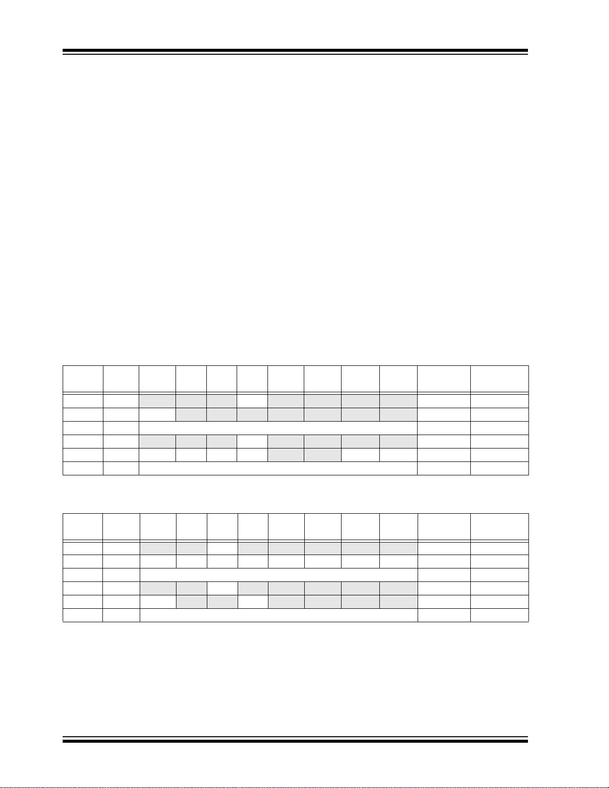
PIC16F627A/628A/648A
12.5.2 USART SYNCHRONOUS SLAVE RECEPTION
The operation of the Synchronous Master and Slave
modes is identical except in the case of the Sleep
mode. Also, bit SREN is a “don’t care” in Slave mode.
If receive is enabled by setting bit CREN prior to the
SLEEP instruction, then a w ord m ay be rec eived durin g
Sleep. On completely receiving the word, the RSR
register will transfer the data to the RCREG register
and if enable bit RCIE bit is set, the int errupt generate d
will wake the chip from Sleep. If the global interrupt is
enabled, the program w ill br anch to the interru pt vec tor
(0004h).
Follow these steps when setting up a Synchronous
Slave Reception:
1. TRISB<1> and TRISB<2> should both be set to
‘1’ to configure the RB1/RX / DT an d R B2/ TX/C K
pins as inputs. Output drive, when required, is
controlled by the peripheral circuitry.
2. Enable the synchronous master serial port by
setting bits SYNC and SPEN and clearing bit
CSRC.
3. If interrupts are desired, then set enable bit
RCIE.
4. If 9-bit reception is desired, then set bit RX9.
5. To enable reception, set enable bit CREN.
6. Flag bit RCIF will be set when reception is
complete and an interrupt will be generated, if
enable bit RCIE was set.
7. Read the RCSTA register to get the ninth bit (if
enabled) and determine if any error occurred
during reception.
8. Read the 8-bit received data by reading the
RCREG register.
9. If an OERR error occurred, clear the error by
clearing bit CREN.
TABLE 12-11: REGISTERS ASSOCIATED WITH SYNCHRONOUS SLAVE TRANSMISSION
Address Name Bit 7 Bit 6 Bit 5 Bit 4 Bit 3 Bit 2 Bit 1 Bit 0
0Ch PIR1
18h RCSTA SPEN RX9 SREN CREN ADEN FERR OERR RX9 D 0000 000x 0000 000x
19h TXREG USART Transmit Data Register 0000 0000 0000 0000
8Ch PIE1
98h TXSTA CSRC TX9 TXEN SYNC
99h SPBRG Baud Rate Generator Register 0000 0000 0000 0000
Legend: x = unknown, - = unimplemented read as ‘0’. Shaded cells are not used for sy nchronous slave transmi ssion.
EEIF CMIF RCIF TXIF — CCP1IF TMR2IF TMR1IF 0000 -000 0000 -000
EEIE CMIE RCIE TX IE — CCP1IE TMR2IE TM R1IE 0000 -000 0000 -000
— BRGH TRMT TX9D 0000 -010 0000 -010
Value on
POR
Value on all
other Resets
TABLE 12-12: REGISTERS ASSOCIATED WITH SYNCHRONOUS SLAVE RECEPTION
Address Name Bit 7 Bit 6 Bit 5 Bit 4 Bit 3 Bit 2 Bit 1 Bit 0
0Ch PIR1
18h RCSTA SPEN RX9
1Ah RCREG USART Receive Data Register 0000 0000 0000 0000
8Ch PIE1
98h TXSTA CSRC TX9 TXEN SYNC — BRGH TRMT TX9D 0000 -010 0000 -010
99h SPBRG Baud Rate Gener ator Reg ister 0000 0000 0000 0000
Legend: x = unknown, - = unimplemented read as ‘0’. Shaded cells are not used for synchronous slave rece pt io n.
DS40044F-page 88 © 2007 Microchip Technology Inc.
EEIF CMIF RCIF TXIF — CCP1IF TMR2IF TMR1IF 0000 -000 0000 -000
SREN CREN ADEN FERR OERR RX9D 0000 000x 0000 000x
EEIE CMIE RCIE TXIE — CCP1IE TMR2IE TMR1IE 0000 -000 0000 -000
Val ue on
POR
Value on all
other Resets

PIC16F627A/628A/648A
13.0 DATA EEPROM MEMORY
The EEPROM data memory is readable and writable
during normal operation (full V
is not directly mapp ed in the register fil e spa ce. Instead
it is indirectly addressed through the Special Function
Registers (SFRs). There are four SFRs used to read
and write this memory. These registers are:
• EECON1
• EECON2 (Not a physically implemented register)
• EEDATA
• EEADR
EEDA TA holds the 8-bit d ata for read/write a nd EEADR
holds the address of the EEPROM location being
accessed. PIC16F627A/628A devices have 128 bytes
of data EEPROM with an address range from 0h to
7Fh. The PIC16F648A device has 256 bytes of data
EEPROM with an address range from 0h to FFh.
DD range). This memory
The EEPROM data memory allows b yte read and write.
A byte write automatically erases the location and
writes the new data (erase be fore write). The EEPROM
data memory is rated fo r high er ase/writ e cycles. T he
write time is controlled by an on-chip timer. The write
time will vary with voltage and temperature, as well as
from chip-t o -ch ip . Pl ea se re f er to A C sp ec i fica t i on s for
exact limits.
When the device is code-protected, the CPU can
continue to read and write the data EEPROM memory. A
device programmer can no longer access this memory.
Additional information on the data EEPROM is
available in the PIC
(DS33023).
®
Mid-Range Reference Manual
REGISTER 13-1: EEDATA – EEPROM DATA REGISTER (ADDRESS: 9Ah)
R/W-x R/W-x R/W-x R/W-x R/W-x R/W-x R/W-x R/W-x
EEDAT7 EEDAT6 EEDAT5 EEDAT4 EEDAT3 EEDAT2 EEDAT1 EEDAT0
bit 7 bit 0
bit 7-0 EEDATn: Byte value to Write to or Read from data EEPROM memory location.
Legend:
R = Readable bit W = Writable bit U = Unimplemented bit, read as ‘0’
-n = Value at POR ‘1’ = Bit is set ‘0’ = Bit is cleared x = Bit is unknown
REGISTER 13-2: EEADR – EEPROM ADDRESS REGISTER (ADDRESS: 9Bh)
R/W-x R/W-x R/W-x R/W-x R/W-x R/W-x R/W-x R/W-x
EADR7 EADR6 EADR5 EADR4 EADR3 EADR2 EADR1 EADR0
bit 7 bit 0
bit 7 PIC16F627A/628A
Unimplemented Address: Must be set to ‘0’
PIC16F648A
EEADR: Set to ‘1’ specifies top 128 locations (128-255) of EEPROM Read/Write Operation
bit 6-0 EEADR: Specifies one of 128 locations of EEPROM Read/Write Operation
Legend:
R = Readable bit W = Writable bit U = Unimplemented bit, read as ‘0’
-n = Value at POR ‘1’ = Bit is set ‘0’ = Bit is cleared x = Bit is unknown
© 2007 Microchip Technology Inc. DS40044F-page 89

PIC16F627A/628A/648A
13.1 EEADR
The PIC16F648A EEADR register addresses 256
bytes of data EEPROM. All eight bits in the register
(EEADR<7:0>) are required.
The PIC16F627A/628A EEADR register addresses
only the first 128 bytes o f dat a EEPROM so only seven
of the eight bits in the register (EEADR<6:0>) are
required. The upper bit is address decoded. This
means that this bit should always be ‘0’ to ensure that
the address is in the 128 byte memory space.
13.2 EECON1 and EECON2 Registers
EECON1 is the control register with four low order bits
physically implemented. The upper-four bits are nonexistent and read as ‘0’s.
Control bits RD and WR initiate read and write,
respectiv el y. These bits ca nno t be cl ea re d, on ly s et, in
software. They are cleared in hardware at completion
of the read or write operation. The inability to clear the
WR bit in software prevents the accidental, premature
termination of a write operation.
The WREN bit, when set, will allow a write operation.
On power-up, the WREN bit is c lear . T he WRERR bit is
set when a write operation is interrupted by a MCLR
Reset or a WDT Time-out Reset during normal
operation. In these situ ations, fol lowing Re set, the user
can check the WRERR bit and rew rite the location. Th e
data and address will be unchanged in the EEDATA
and EEADR registers.
Interrupt flag bit EEIF in the PIR1 register is set when
write is complete. This bit must be cleared in software.
EECON2 is not a physical register. Reading EECON2
will read all ‘0’s. The EECON2 register is used
exclusively in the data EEPROM write sequence.
REGISTER 13-3: EECON1 – EEPROM CONTROL REGISTER 1 (ADDRESS: 9Ch)
U-0 U-0 U-0 U-0 R/W-x R/W-0 R/S-0 R/S-0
— — — — WRERR WREN WR RD
bit 7 bit 0
bit 7-4 Unimplemented: Read as ‘0’
bit 3 WRERR: EEPROM Error Flag bit
1 = A write operation is prematurely terminated (any MCLR
normal operation or BOR Reset)
0 = The write operati on compl eted
bit 2 WREN: EEPROM Write Enable bit
1 = Allows write cycles
0 = Inhibits write to the data EEPROM
bit 1 WR: Write Control bit
1 = initiates a write cycle. (The bit is cleared by hardware once write is complete. The WR bit
can only be set (not cleared) in software.
0 = Write cycle to the data EEPROM is complete
bit 0 RD: Read Control bit
1 = Initiates an EEPROM read (read takes one cycle. RD is cleared in hardware. The RD bit
can only be set (not cleared) in software).
0 = Does not initiate an EEPROM read
Legend:
R = Readable bit W = Writable bit U = Unimplemented bit, read as ‘0’
-n = Value at POR ‘1’ = Bit is set ‘0’ = Bit is cleared x = Bit is unknown
Reset, any WDT Reset during
DS40044F-page 90 © 2007 Microchip Technology Inc.

PIC16F627A/628A/648A
13.3 Reading the EEPROM Data
Memory
T o read a d ata memory loca tion, the user must write the
address to the EEADR register and then set control bit
RD (EECON1<0>). The data is available, in the very
next cycle, in the EEDATA register; therefore it can be
read in the next instructi on. EEDATA will hol d this value
until another read or until it is written to by the user
(during a write operation).
EXAMPLE 13-1: DATA EEPROM READ
BSF STATUS, RP0 ;Bank 1
MOVLW CONFIG_ADDR ;
MOVWF EEADR ;Address to read
BSF EECON1, RD ;EE Read
MOVF EEDATA, W ;W = EEDATA
BCF STATUS, RP0 ;Bank 0
13.4 Writing to the EEPROM Data Memory
To write an EEPROM data location, the user must first
write the address to the EEADR register and the data
to the EEDATA register. Then the user must follow a
specific sequence to initiate the write for each byte.
EXAMPLE 13-2: DATA EEPROM WRITE
BSF STATUS, RP0 ;Bank 1
BSF EECON1, WREN ;Enable write
BCF INTCON, GIE ;Disable INTs.
BTFSC INTCON,GIE ;See AN576
GOTO $-2
MOVLW 55h ;
MOVWF EECON2 ;Write 55h
MOVLW AAh ;
MOVWF EECON2 ;Write AAh
Required
Sequence
BSF EECON1,WR ;Set WR bit
;begin write
BSF INTCON, GIE ;Enable INTs.
The write will not initiate if the above sequence is not
followed exactly (write 55h to EECON2, write AAh to
EECON2, then set WR bit) for each byte. We strongly
recommend that interrupts be disabled during this
code segment. A cycle count is executed during the
required sequence. A ny number th at is not equa l to the
required cycles to execute the required sequence will
cause the data not to be written into the EEPROM.
Additionally, the WREN bit in EECON1 must be set to
enable write. This mechanism prevents accidental
writes to data EEPROM due to errant (unexpected)
code execution (i.e., lost programs). The user should
keep the WREN bit clear at all times, except when
updating EEPROM. The WREN bit is not cleared
by hardware.
After a write sequence has been initiated, clearing the
WREN bit will not af fect this wri te cycle. The W R bit will
be inhibited from being set unless the WREN bit is set.
At the completion of the write cycle, the WR bit is
cleared in hardware and the EE Write Complete
Interrupt Flag bit (EEIF) is set. The user can either
enable this interrupt or poll this bit. The EEIF bit in the
PIR1 registers must be cleared by software.
13.5 Write Verify
Depending on the application, good programming
practice may dictate that the value written to the Data
EEPROM should be verified (Example 13-3) to the
desired value to be written. This should be used in
applications where an EEPROM bit will be stressed
near the specification limit.
EXAMPLE 13-3: WRITE VERIFY
BSF STATUS, RP0 ;Bank 1
MOVF EEDATA, W
BSF EECON1, RD ;Read the
;value written
;
;Is the value written (in W reg) and
;read (in EEDATA) the same?
;
SUBWF EEDATA, W ;
BTFSS STATUS, Z ;Is difference 0?
GOTO WRITE_ERR ;NO, Write error
: ;YES, Good write
: ;Continue program
13.6 Protection Against Spurious Write
There are conditions when the device may not want to
write to the data EEPROM memory. To protect against
spurious EEPROM writes, various mechanisms have
been built-in. On power-up, WREN is cleared. Also
when enabled, the Power-up Timer (72 ms duration)
prevents EEPROM write.
The write initiate sequence and the WREN bi t tog eth er
help prevent an accidental write during brown-out,
power glitch or software malfunction.
© 2007 Microchip Technology Inc. DS40044F-page 91

PIC16F627A/628A/648A
13.7 Using the Data EEPROM
The data EEPROM is a high endurance, byte
A simple data EEPROM refresh routine is shown in
Example 13-4.
addressable array that has been optimized for the storage
of frequently changing information (e.g., program
variables or other data that are updated often). When
variables in one section change frequently, while
variables in another section do not change, it is possible
to exceed the total number of write cycles to the EEPROM
(specification D124) without exceeding the total number
of write cycles to a single byte (specifications D120 and
D120A). If this is the case, then an array refresh must be
performed. For this reason, variables that change
infrequently (such as constants, IDs, calibration, etc.)
should be stored in Flash program memory .
EXAMPLE 13-4: DATA EEPROM REFRESH ROUTINE
BANKSEL 0X80 ;select Bank1
CLRF EEADR ;start at address 0
BCF INTCON, GIE ;disable interrupts
BTFSC INTCON, GIE ;see AN576
GOTO $ - 2
BSF EECON1, WREN ;enable EE writes
Loop
BSF EECON1, RD ;retrieve data into EEDATA
MOVLW 0x55 ;first step of ...
MOVWF EECON2 ;... required sequence
MOVLW 0xAA ;second step of ...
MOVWF EECON2 ;... required sequence
BSF EECON1, WR ;start write sequence
BTFSC EECON1, WR ;wait for write complete
GOTO $ - 1
Note: If data EEPROM is only used to store
constants an d/or data that changes rarely ,
an array refresh is likely not required. See
specification D124.
#IFDEF __16F648A ;256 bytes in 16F648A
INCFSZ EEADR, f ;test for end of memory
#ELSE ;128 bytes in 16F627A/628A
INCF EEADR, f ;next address
BTFSS EEADR, 7 ;test for end of memory
#ENDIF ;end of conditional assembly
GOTO Loop ;repeat for all locations
BCF EECON1, WREN ;disable EE writes
BSF INTCON, GIE ;enable interrupts (optional)
DS40044F-page 92 © 2007 Microchip Technology Inc.
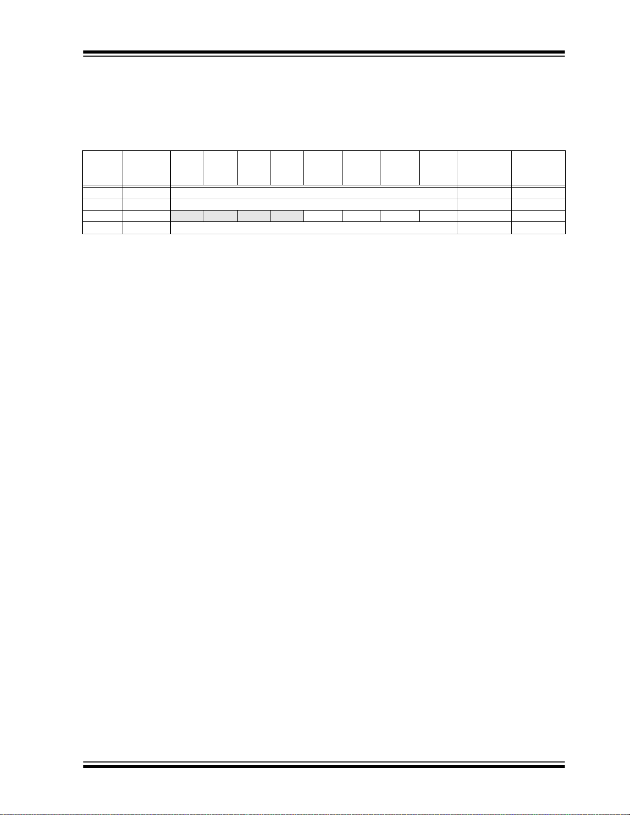
PIC16F627A/628A/648A
13.8 Data EEPROM Operation During Code-Protect
When the device is code-protected, the CPU is able to
read and write data to the data EEPROM.
TABLE 13-1: REGISTERS/BITS ASSOCIATED WITH DATA EEPROM
Address Name Bit 7 Bit 6 Bit 5 Bit 4 Bit 3 Bit 2 Bit 1 Bit 0
9Ah EEDATA E EP RO M Data Register xxxx xxxx uuuu uuuu
9Bh EEADR EEPROM Address Register xxxx xxxx uuuu uuuu
9Ch EECON1
9Dh EECON2
Legend: x = unknown, u = unchanged, - = unimplemented read as ‘0’, q = value depends upon condition.
Shaded cells are not used by data EEPROM.
Note 1: EECON2 is not a physical register.
— — — — WRERR WREN WR RD ---- x000 ---- q000
(1)
EEPROM Control Register 2 ---- ---- ---- ----
Val ue on
Power-on
Reset
Value on all
other
Resets
© 2007 Microchip Technology Inc. DS40044F-page 93

PIC16F627A/628A/648A
NOTES:
DS40044F-page 94 © 2007 Microchip Technology Inc.

PIC16F627A/628A/648A
14.0 SPECIAL FEATURES OF THE CPU
Special circuits to deal with the needs of real-time
applications are what sets a microcontroller apart from
other processors. The PIC16F627A/628A/648A family
has a host of such features intended to maximize
system reliability, minimize cost through elimination of
external components, provide power-saving operating
modes and offer code prote cti on.
These are:
1. OSC select ion
2. Reset
3. Power-on Reset (POR)
4. Power-up Timer (PWRT)
5. Oscillator Start-Up Timer (OST)
6. Brown-o ut Reset (BOR)
7. Interrupts
8. Watchdog Timer (WDT)
9. Sleep
10. Code protection
11. ID Locations
12. In-Circuit Serial Programming™ (ICSP™)
The PIC16F627A/628A/648A has a Watchdog Timer
which is controlled by configuration bits. It runs off its
own RC oscillator for added reliability. There are two
timers that offe r necessa ry delay s on po wer-up. O ne is
the Oscillator Start-up Timer (OST), intended to keep
the chip in Reset until the crystal oscillator is stable.
The other is the Power-up Timer (PWRT), which
provides a fixed delay of 72 ms (nominal) on power-up
only, designed to keep the part in Reset while the
power supply stabilizes. There is also circuitry to reset
the device if a brown-out occurs. With these three
functions on-chip, most applications need no external
Reset circuitry.
The Sleep mode is designed to offer a very low curre nt
Power-down mode. The user can wake-up from Sleep
through external Reset, Watchdog Timer wake-up or
through an interrupt. Several osci llator option s are also
made availab le to allow the par t to fit the applic ation.
The RC oscilla tor option sa ves system cos t while the
LP crystal option saves power. A set of configuration
bits are used to select various options.
14.1 Configuration Bits
The configuration bits can be programmed (r ead as ‘0’)
or left unprogrammed (read as ‘1’) to select various
device configurations. These bits are mapped in
program memory location 2007h.
The user will note that address 2007h is beyond the
user program memory space. In fact, it belongs to the
special configuration memory space (2000h-3FFFh),
which can be accessed only during programming. See
“PIC16F627A/628A/648A EEPROM Memory
Programming Specification” (DS41196) for additional
information.
© 2007 Microchip Technology Inc. DS40044F-page 95

PIC16F627A/628A/648A
REGISTER 14-1: CONFIG – CONFIGURATION WORD REGISTER
CP — — — —CPDLVP BOREN MCLRE FOSC2 PWRTE WDTE F0SC1 F0SC0
bit 13 bit 0
bit 13: CP: Flash Program Memory Code Protection bit
bit 12-9: Unimplemented: Read as ‘0’
bit 8: CPD
bit 7: LVP: Low-Voltage Programming Enable bit
bit 6: BOREN: Brown-out Reset Enable bit
bit 5: MCLRE: RA5/MCLR
bit 3: PWRTE: Power-up Timer Enable bit
(PIC16F648A)
1 = Code protection off
0 = 0000h to 0FFFh code-protected
(
PIC16F628A)
1 = Code protection off
0 = 0000h to 07FFh code-protected
(
PIC16F627A)
1 = Code protection off
0 = 0000h to 03FFh code-protected
: Data Code Protection bit
1 = Data memory code protection off
0 = Data memory code-protected
1 = RB4/PGM pin has PGM function, low-voltage programming enabled
0 = RB4/PGM is digital I/O, HV on MCLR
1 = BOR Reset enabled
0 = BOR Reset disabled
1 = RA5/MCLR/
0 = RA5/MCLR/
1 = PWRT disabled
0 = PWRT enabled
/VPP Pin Function Select bit
VPP pin function is MCLR
VPP pin function is digital Input, MCLR internally tied to VDD
(3)
must be used for programming
(1)
(1)
(2)
bit 2: WDTE: Watchdog Timer Enable bit
bit 4, 1-0: FOSC<2:0>: Oscillator Selection bits
1 = WDT enabled
0 = WDT disabled
111 = RC oscillator: CLKOUT function on RA6/OSC2/CLKOUT pin, Resistor and Capacit or on RA7/OS C1 /CLKIN
110 = RC oscillator: I/O function on RA6/OSC2/CLKOUT pi n, Resistor and Capacitor on RA7/OSC1/CLKIN
101 = INTOSC oscillator: CLKOUT function on RA6/OSC2/CLKOUT pin, I/O function on RA7/OSC1/CLKIN
100 = INTOSC oscillator: I/O function on RA6/OSC2/CLKOUT pin, I/O function on RA7/OSC1/CLKIN
011 = EC: I/O function on RA6/OSC2/CLKOUT pin, CLKIN on RA7/OSC1/CLKIN
010 = HS oscillator: High-speed crystal/resonator on RA6/OSC2/CLKOUT and RA7/OSC1/CLKIN
001 = XT oscillator: Crystal/resonator on RA6/OSC2/CLKOUT and RA7/OSC1/CLKIN
000 = LP oscillator: Low-power crystal on RA6/OSC2/CLKOUT and RA7/OSC1/CLKIN
Note 1: Enabling Brown-out Reset does not automatically enable the Power-up Timer (PWRT) the way it does on the
Legend:
R = Readable bit W = Writable bit U = Unimplemented bit, read as ‘0’
-n = Value at POR ‘1’ = bit is set ‘0’ = bit is cleared x = bit is unknown
PIC16F627/628 devices.
2: The code protection scheme has changed from the code protection scheme used on the PIC16F627/628 devices. The
entire Flash program memory needs to be bulk erased to set the CP bit, turning the code protection off. See
“PIC16F627A/628A/648A EEPROM Memory Programming Specification” (DS41196) for details.
3: The entire data EEPROM needs to be bulk erased to set the CPD
628A/648A EEPROM Memory Programming Specification” (DS41196) for details.
4: When MCLR
is asserted in INTOSC mode, the internal clock oscillator is disabled.
(4)
bit, turning the code protection off. See “PIC16F627A/
DS40044F-page 96 © 2007 Microchip Technology Inc.

PIC16F627A/628A/648A
14.2 Oscillator Configurations
14.2.1 OSCILLATOR TYPES
The PIC16F627A/628A/648A can be operated in eight
different osci llator optio ns. The user c an program thre e
configuration bits (FOSC2 through FOSC0) to select
one of these eight modes:
• LP Low Power Crystal
• XT Crystal/Resonator
• HS High Speed Crystal/Resonator
• RC External Resistor/Cap ac ito r (2 modes )
• INTOSC Internal Precision Oscillator (2 modes)
• EC External Clock In
14.2.2 CRYSTAL OSCILLATOR / CERAMIC
RESONATORS
In XT, LP or HS modes a crystal or ceramic resonator
is connected to the OSC1 and OSC2 pins to establish
oscillation (Figure14-1). The PIC16F627A/628A/648A
oscillator design requires the use of a parallel cut
crystal. Use of a series cut crystal may give a frequency
out of the cryst al manufact urers specifica tions. When in
XT, LP or HS modes, the device can have an external
clock source to drive the OSC1 pin (Figure 14-4).
FIGURE 14-1: CRYSTAL OPERATION
(OR CERAMIC RESONATOR)
(HS, XT OR LP OSC
CONFIGURATION)
OSC1
(2)
C1
XTAL
OSC2
(1)
RS
(2)
C2
Note 1: A series resistor may be required for AT strip cut
crystals.
2: See Table 14-1 and Table 14-2 for recommended
values of C1 and C2.
RF
PIC16F627A/628A/648A
Sleep
FOSC
T ABLE 14-1: CAPACITOR SELECTION FOR
CERAMIC RESONATORS
Mode Freq OSC1(C1) OSC2(C2)
XT 455 kHz
2.0 MHz
4.0 MHz
HS 8.0 MHz
16.0 MHz
22-100 pF
15-68 pF
15-68 pF
10-68 pF
10-22 pF
22-100 pF
15-68 pF
15-68 pF
10-68 pF
10-22 pF
Note: Higher capacitance increases the stability
of the oscillator, but also increases the
start-up time. These values are for design
guidance only. Since each resonator has
its own characteristics, the user should
consult the resonator manufacturer for
appropriate values of external components.
T ABLE 14-2: CAPACITOR SELECTION FOR
CRYSTAL OSCILLATOR
Mode Freq OSC1(C1) OSC2(C2)
LP 32 kHz
200 kHz
XT 100 kHz
2 MHz
4 MHz
HS 8 MHz
10 MHz
20 MHz
Note: Higher capacitance increases the stability
of the oscillator, but also increases the
start-up time. These values are for design
guidance only. A series resistor (RS) may
be required in HS mode, as well as XT
mode, to avoid overdriving crystals with
low drive level specification. Since each
crystal has its own characteristics, the
user should consult the crystal manufacturer for appropriate values of external
components.
15-30 pF
0-15 pF
68-150 pF
15-30 pF
15-30 pF
15-30 pF
15-30 pF
15-30 pF
15-30 pF
0-15 pF
150-200 pF
15-30 pF
15-30 pF
15-30 pF
15-30 pF
15-30 pF
© 2007 Microchip Technology Inc. DS40044F-page 97

PIC16F627A/628A/648A
/
14.2.3 EXTERNAL CRYSTAL OSCILLATOR CIRCUIT
Either a prepackage d oscillator can be used or a simple
oscillator circuit with TTL gates can be built.
Prepackaged oscillators provide a wide operating
range and better stability. A well-designed crystal
oscillator will provide good performance with TTL
gates. Two types of crystal oscillator circuits can be
used; one with series resonance, or one with parallel
resonance.
Figure 14-2 shows implementation of a parallel
resonant oscillator circuit. The circuit is designed to
use the fundamental frequency of the crystal. The
74AS04 inverter per forms th e 180° ph ase shift that a
parallel oscillator requires. The 4.7 kΩ resistor
provides the negative feedback for stability. The
10 kΩ potenti ometers bias the 74AS04 i n the linear
region. This could be used for external oscillator
designs.
FIGURE 14-2: EXTERNAL PARALLEL
RESONANT CRYSTAL
OSCILLATOR CIRCUIT
+5V
10K
4.7K
74AS04
74AS04
To other
Devices
PIC16F627A/628A/648A
CLKIN
FIGURE 14-3: EXTERNAL SERIES
RESONANT CRYSTAL
OSCILLATOR CIRCUIT
330 KΩ
74AS04
330 KΩ
74AS04
0.1 pF
XTAL
14.2.4 PRECISION INTERNAL 4 MH
To other
74AS04
Devices
CLKIN
PIC16F627A
628A/648A
Z
OSCILLATOR
The internal precisi on os cilla tor pr ovid es a f ixed 4MHz
(nominal) system clock at V
DD = 5V and 25°C. See
Section 17.0 “Electrical Specifications”, for inform ation on variation over voltage and temperature.
14.2.5 EXTERNAL CLOCK IN
For applications where a clock is already available
elsewhere, users may directly drive the PIC16F627A/
628A/648A provided that this external clock source meets
the AC/DC timing requirements listed in Section 17.6
“Timing Diagrams and Specifications”. Figure 14-4
below shows how an external clock circuit should be
configured.
10K
XTAL
10K
C1 C2
Figure 14-3 shows a series resonant oscillator circuit.
This circuit is also designed to use the fundamental
frequency of the crystal. The inverter performs a 180°
phase shift in a series resonant oscillator circuit. The
330 kΩ resistors provide the negative fee dback to bias
the inverters in their linear region.
FIGURE 14-4: EXTERNAL CLOCK INPUT
OPERATION (EC, HS, XT
OR LP OSC
CONFIGURATION)
Clock from
ext. system
RA6
RA7/OSC1/CLKIN
PIC16F627A/628A/648A
RA6/OSC2/CLKOUT
DS40044F-page 98 © 2007 Microchip Technology Inc.
 Loading...